KR102530338B1 - Semiconductor device and method for fabricating the same - Google Patents
Semiconductor device and method for fabricating the sameDownload PDFInfo
- Publication number
- KR102530338B1 KR102530338B1KR1020160171662AKR20160171662AKR102530338B1KR 102530338 B1KR102530338 B1KR 102530338B1KR 1020160171662 AKR1020160171662 AKR 1020160171662AKR 20160171662 AKR20160171662 AKR 20160171662AKR 102530338 B1KR102530338 B1KR 102530338B1
- Authority
- KR
- South Korea
- Prior art keywords
- pattern
- semiconductor substrate
- isolation trench
- sidewall
- insulating layer
- Prior art date
- Legal status (The legal status is an assumption and is not a legal conclusion. Google has not performed a legal analysis and makes no representation as to the accuracy of the status listed.)
- Active
Links
Images


Classifications
- H—ELECTRICITY
- H10—SEMICONDUCTOR DEVICES; ELECTRIC SOLID-STATE DEVICES NOT OTHERWISE PROVIDED FOR
- H10D—INORGANIC ELECTRIC SEMICONDUCTOR DEVICES
- H10D30/00—Field-effect transistors [FET]
- H10D30/60—Insulated-gate field-effect transistors [IGFET]
- H10D30/611—Insulated-gate field-effect transistors [IGFET] having multiple independently-addressable gate electrodes influencing the same channel
- H—ELECTRICITY
- H01—ELECTRIC ELEMENTS
- H01L—SEMICONDUCTOR DEVICES NOT COVERED BY CLASS H10
- H01L25/00—Assemblies consisting of a plurality of semiconductor or other solid state devices
- H01L25/03—Assemblies consisting of a plurality of semiconductor or other solid state devices all the devices being of a type provided for in a single subclass of subclasses H10B, H10D, H10F, H10H, H10K or H10N, e.g. assemblies of rectifier diodes
- H01L25/04—Assemblies consisting of a plurality of semiconductor or other solid state devices all the devices being of a type provided for in a single subclass of subclasses H10B, H10D, H10F, H10H, H10K or H10N, e.g. assemblies of rectifier diodes the devices not having separate containers
- H01L25/07—Assemblies consisting of a plurality of semiconductor or other solid state devices all the devices being of a type provided for in a single subclass of subclasses H10B, H10D, H10F, H10H, H10K or H10N, e.g. assemblies of rectifier diodes the devices not having separate containers the devices being of a type provided for in group subclass H10D
- H01L25/074—Stacked arrangements of non-apertured devices
- H01L29/7831—
- H—ELECTRICITY
- H10—SEMICONDUCTOR DEVICES; ELECTRIC SOLID-STATE DEVICES NOT OTHERWISE PROVIDED FOR
- H10D—INORGANIC ELECTRIC SEMICONDUCTOR DEVICES
- H10D86/00—Integrated devices formed in or on insulating or conducting substrates, e.g. formed in silicon-on-insulator [SOI] substrates or on stainless steel or glass substrates
- H10D86/201—Integrated devices formed in or on insulating or conducting substrates, e.g. formed in silicon-on-insulator [SOI] substrates or on stainless steel or glass substrates the substrates comprising an insulating layer on a semiconductor body, e.g. SOI
- H10D86/215—Integrated devices formed in or on insulating or conducting substrates, e.g. formed in silicon-on-insulator [SOI] substrates or on stainless steel or glass substrates the substrates comprising an insulating layer on a semiconductor body, e.g. SOI comprising FinFETs
- H—ELECTRICITY
- H01—ELECTRIC ELEMENTS
- H01L—SEMICONDUCTOR DEVICES NOT COVERED BY CLASS H10
- H01L21/00—Processes or apparatus adapted for the manufacture or treatment of semiconductor or solid state devices or of parts thereof
- H01L21/02—Manufacture or treatment of semiconductor devices or of parts thereof
- H01L21/04—Manufacture or treatment of semiconductor devices or of parts thereof the devices having potential barriers, e.g. a PN junction, depletion layer or carrier concentration layer
- H01L21/18—Manufacture or treatment of semiconductor devices or of parts thereof the devices having potential barriers, e.g. a PN junction, depletion layer or carrier concentration layer the devices having semiconductor bodies comprising elements of Group IV of the Periodic Table or AIIIBV compounds with or without impurities, e.g. doping materials
- H01L21/185—Joining of semiconductor bodies for junction formation
- H—ELECTRICITY
- H01—ELECTRIC ELEMENTS
- H01L—SEMICONDUCTOR DEVICES NOT COVERED BY CLASS H10
- H01L21/00—Processes or apparatus adapted for the manufacture or treatment of semiconductor or solid state devices or of parts thereof
- H01L21/02—Manufacture or treatment of semiconductor devices or of parts thereof
- H01L21/04—Manufacture or treatment of semiconductor devices or of parts thereof the devices having potential barriers, e.g. a PN junction, depletion layer or carrier concentration layer
- H01L21/18—Manufacture or treatment of semiconductor devices or of parts thereof the devices having potential barriers, e.g. a PN junction, depletion layer or carrier concentration layer the devices having semiconductor bodies comprising elements of Group IV of the Periodic Table or AIIIBV compounds with or without impurities, e.g. doping materials
- H01L21/30—Treatment of semiconductor bodies using processes or apparatus not provided for in groups H01L21/20 - H01L21/26
- H01L21/302—Treatment of semiconductor bodies using processes or apparatus not provided for in groups H01L21/20 - H01L21/26 to change their surface-physical characteristics or shape, e.g. etching, polishing, cutting
- H01L21/306—Chemical or electrical treatment, e.g. electrolytic etching
- H01L21/30604—Chemical etching
- H—ELECTRICITY
- H01—ELECTRIC ELEMENTS
- H01L—SEMICONDUCTOR DEVICES NOT COVERED BY CLASS H10
- H01L21/00—Processes or apparatus adapted for the manufacture or treatment of semiconductor or solid state devices or of parts thereof
- H01L21/02—Manufacture or treatment of semiconductor devices or of parts thereof
- H01L21/04—Manufacture or treatment of semiconductor devices or of parts thereof the devices having potential barriers, e.g. a PN junction, depletion layer or carrier concentration layer
- H01L21/18—Manufacture or treatment of semiconductor devices or of parts thereof the devices having potential barriers, e.g. a PN junction, depletion layer or carrier concentration layer the devices having semiconductor bodies comprising elements of Group IV of the Periodic Table or AIIIBV compounds with or without impurities, e.g. doping materials
- H01L21/30—Treatment of semiconductor bodies using processes or apparatus not provided for in groups H01L21/20 - H01L21/26
- H01L21/31—Treatment of semiconductor bodies using processes or apparatus not provided for in groups H01L21/20 - H01L21/26 to form insulating layers thereon, e.g. for masking or by using photolithographic techniques; After treatment of these layers; Selection of materials for these layers
- H01L21/3105—After-treatment
- H01L21/311—Etching the insulating layers by chemical or physical means
- H01L21/31105—Etching inorganic layers
- H01L21/31111—Etching inorganic layers by chemical means
- H—ELECTRICITY
- H01—ELECTRIC ELEMENTS
- H01L—SEMICONDUCTOR DEVICES NOT COVERED BY CLASS H10
- H01L21/00—Processes or apparatus adapted for the manufacture or treatment of semiconductor or solid state devices or of parts thereof
- H01L21/02—Manufacture or treatment of semiconductor devices or of parts thereof
- H01L21/04—Manufacture or treatment of semiconductor devices or of parts thereof the devices having potential barriers, e.g. a PN junction, depletion layer or carrier concentration layer
- H01L21/50—Assembly of semiconductor devices using processes or apparatus not provided for in a single one of the groups H01L21/18 - H01L21/326 or H10D48/04 - H10D48/07 e.g. sealing of a cap to a base of a container
- H—ELECTRICITY
- H01—ELECTRIC ELEMENTS
- H01L—SEMICONDUCTOR DEVICES NOT COVERED BY CLASS H10
- H01L21/00—Processes or apparatus adapted for the manufacture or treatment of semiconductor or solid state devices or of parts thereof
- H01L21/70—Manufacture or treatment of devices consisting of a plurality of solid state components formed in or on a common substrate or of parts thereof; Manufacture of integrated circuit devices or of parts thereof
- H01L21/71—Manufacture of specific parts of devices defined in group H01L21/70
- H01L21/76—Making of isolation regions between components
- H01L21/762—Dielectric regions, e.g. EPIC dielectric isolation, LOCOS; Trench refilling techniques, SOI technology, use of channel stoppers
- H01L21/7624—Dielectric regions, e.g. EPIC dielectric isolation, LOCOS; Trench refilling techniques, SOI technology, use of channel stoppers using semiconductor on insulator [SOI] technology
- H01L21/76251—Dielectric regions, e.g. EPIC dielectric isolation, LOCOS; Trench refilling techniques, SOI technology, use of channel stoppers using semiconductor on insulator [SOI] technology using bonding techniques
- H—ELECTRICITY
- H01—ELECTRIC ELEMENTS
- H01L—SEMICONDUCTOR DEVICES NOT COVERED BY CLASS H10
- H01L21/00—Processes or apparatus adapted for the manufacture or treatment of semiconductor or solid state devices or of parts thereof
- H01L21/70—Manufacture or treatment of devices consisting of a plurality of solid state components formed in or on a common substrate or of parts thereof; Manufacture of integrated circuit devices or of parts thereof
- H01L21/71—Manufacture of specific parts of devices defined in group H01L21/70
- H01L21/76—Making of isolation regions between components
- H01L21/762—Dielectric regions, e.g. EPIC dielectric isolation, LOCOS; Trench refilling techniques, SOI technology, use of channel stoppers
- H01L21/7624—Dielectric regions, e.g. EPIC dielectric isolation, LOCOS; Trench refilling techniques, SOI technology, use of channel stoppers using semiconductor on insulator [SOI] technology
- H01L21/76264—SOI together with lateral isolation, e.g. using local oxidation of silicon, or dielectric or polycristalline material refilled trench or air gap isolation regions, e.g. completely isolated semiconductor islands
- H01L21/76283—Lateral isolation by refilling of trenches with dielectric material
- H—ELECTRICITY
- H01—ELECTRIC ELEMENTS
- H01L—SEMICONDUCTOR DEVICES NOT COVERED BY CLASS H10
- H01L21/00—Processes or apparatus adapted for the manufacture or treatment of semiconductor or solid state devices or of parts thereof
- H01L21/70—Manufacture or treatment of devices consisting of a plurality of solid state components formed in or on a common substrate or of parts thereof; Manufacture of integrated circuit devices or of parts thereof
- H01L21/71—Manufacture of specific parts of devices defined in group H01L21/70
- H01L21/768—Applying interconnections to be used for carrying current between separate components within a device comprising conductors and dielectrics
- H01L21/76801—Applying interconnections to be used for carrying current between separate components within a device comprising conductors and dielectrics characterised by the formation and the after-treatment of the dielectrics, e.g. smoothing
- H01L21/76829—Applying interconnections to be used for carrying current between separate components within a device comprising conductors and dielectrics characterised by the formation and the after-treatment of the dielectrics, e.g. smoothing characterised by the formation of thin functional dielectric layers, e.g. dielectric etch-stop, barrier, capping or liner layers
- H01L21/823468—
- H—ELECTRICITY
- H01—ELECTRIC ELEMENTS
- H01L—SEMICONDUCTOR DEVICES NOT COVERED BY CLASS H10
- H01L23/00—Details of semiconductor or other solid state devices
- H01L23/52—Arrangements for conducting electric current within the device in operation from one component to another, i.e. interconnections, e.g. wires, lead frames
- H01L23/522—Arrangements for conducting electric current within the device in operation from one component to another, i.e. interconnections, e.g. wires, lead frames including external interconnections consisting of a multilayer structure of conductive and insulating layers inseparably formed on the semiconductor body
- H01L23/5226—Via connections in a multilevel interconnection structure
- H—ELECTRICITY
- H01—ELECTRIC ELEMENTS
- H01L—SEMICONDUCTOR DEVICES NOT COVERED BY CLASS H10
- H01L23/00—Details of semiconductor or other solid state devices
- H01L23/52—Arrangements for conducting electric current within the device in operation from one component to another, i.e. interconnections, e.g. wires, lead frames
- H01L23/522—Arrangements for conducting electric current within the device in operation from one component to another, i.e. interconnections, e.g. wires, lead frames including external interconnections consisting of a multilayer structure of conductive and insulating layers inseparably formed on the semiconductor body
- H01L23/528—Layout of the interconnection structure
- H01L29/4236—
- H01L29/6656—
- H01L29/7849—
- H—ELECTRICITY
- H10—SEMICONDUCTOR DEVICES; ELECTRIC SOLID-STATE DEVICES NOT OTHERWISE PROVIDED FOR
- H10D—INORGANIC ELECTRIC SEMICONDUCTOR DEVICES
- H10D30/00—Field-effect transistors [FET]
- H10D30/01—Manufacture or treatment
- H10D30/021—Manufacture or treatment of FETs having insulated gates [IGFET]
- H10D30/024—Manufacture or treatment of FETs having insulated gates [IGFET] of fin field-effect transistors [FinFET]
- H—ELECTRICITY
- H10—SEMICONDUCTOR DEVICES; ELECTRIC SOLID-STATE DEVICES NOT OTHERWISE PROVIDED FOR
- H10D—INORGANIC ELECTRIC SEMICONDUCTOR DEVICES
- H10D30/00—Field-effect transistors [FET]
- H10D30/60—Insulated-gate field-effect transistors [IGFET]
- H10D30/62—Fin field-effect transistors [FinFET]
- H10D30/6211—Fin field-effect transistors [FinFET] having fin-shaped semiconductor bodies integral with the bulk semiconductor substrates
- H—ELECTRICITY
- H10—SEMICONDUCTOR DEVICES; ELECTRIC SOLID-STATE DEVICES NOT OTHERWISE PROVIDED FOR
- H10D—INORGANIC ELECTRIC SEMICONDUCTOR DEVICES
- H10D30/00—Field-effect transistors [FET]
- H10D30/60—Insulated-gate field-effect transistors [IGFET]
- H10D30/791—Arrangements for exerting mechanical stress on the crystal lattice of the channel regions
- H10D30/798—Arrangements for exerting mechanical stress on the crystal lattice of the channel regions being provided in or under the channel regions
- H—ELECTRICITY
- H10—SEMICONDUCTOR DEVICES; ELECTRIC SOLID-STATE DEVICES NOT OTHERWISE PROVIDED FOR
- H10D—INORGANIC ELECTRIC SEMICONDUCTOR DEVICES
- H10D62/00—Semiconductor bodies, or regions thereof, of devices having potential barriers
- H10D62/10—Shapes, relative sizes or dispositions of the regions of the semiconductor bodies; Shapes of the semiconductor bodies
- H10D62/113—Isolations within a component, i.e. internal isolations
- H10D62/115—Dielectric isolations, e.g. air gaps
- H—ELECTRICITY
- H10—SEMICONDUCTOR DEVICES; ELECTRIC SOLID-STATE DEVICES NOT OTHERWISE PROVIDED FOR
- H10D—INORGANIC ELECTRIC SEMICONDUCTOR DEVICES
- H10D62/00—Semiconductor bodies, or regions thereof, of devices having potential barriers
- H10D62/10—Shapes, relative sizes or dispositions of the regions of the semiconductor bodies; Shapes of the semiconductor bodies
- H10D62/17—Semiconductor regions connected to electrodes not carrying current to be rectified, amplified or switched, e.g. channel regions
- H10D62/213—Channel regions of field-effect devices
- H10D62/221—Channel regions of field-effect devices of FETs
- H10D62/235—Channel regions of field-effect devices of FETs of IGFETs
- H—ELECTRICITY
- H10—SEMICONDUCTOR DEVICES; ELECTRIC SOLID-STATE DEVICES NOT OTHERWISE PROVIDED FOR
- H10D—INORGANIC ELECTRIC SEMICONDUCTOR DEVICES
- H10D64/00—Electrodes of devices having potential barriers
- H10D64/01—Manufacture or treatment
- H10D64/021—Manufacture or treatment using multiple gate spacer layers, e.g. bilayered sidewall spacers
- H—ELECTRICITY
- H10—SEMICONDUCTOR DEVICES; ELECTRIC SOLID-STATE DEVICES NOT OTHERWISE PROVIDED FOR
- H10D—INORGANIC ELECTRIC SEMICONDUCTOR DEVICES
- H10D64/00—Electrodes of devices having potential barriers
- H10D64/20—Electrodes characterised by their shapes, relative sizes or dispositions
- H10D64/27—Electrodes not carrying the current to be rectified, amplified, oscillated or switched, e.g. gates
- H10D64/311—Gate electrodes for field-effect devices
- H10D64/411—Gate electrodes for field-effect devices for FETs
- H10D64/511—Gate electrodes for field-effect devices for FETs for IGFETs
- H10D64/512—Disposition of the gate electrodes, e.g. buried gates
- H10D64/513—Disposition of the gate electrodes, e.g. buried gates within recesses in the substrate, e.g. trench gates, groove gates or buried gates
- H—ELECTRICITY
- H10—SEMICONDUCTOR DEVICES; ELECTRIC SOLID-STATE DEVICES NOT OTHERWISE PROVIDED FOR
- H10D—INORGANIC ELECTRIC SEMICONDUCTOR DEVICES
- H10D84/00—Integrated devices formed in or on semiconductor substrates that comprise only semiconducting layers, e.g. on Si wafers or on GaAs-on-Si wafers
- H10D84/01—Manufacture or treatment
- H10D84/0123—Integrating together multiple components covered by H10D12/00 or H10D30/00, e.g. integrating multiple IGBTs
- H10D84/0126—Integrating together multiple components covered by H10D12/00 or H10D30/00, e.g. integrating multiple IGBTs the components including insulated gates, e.g. IGFETs
- H10D84/0147—Manufacturing their gate sidewall spacers
- H—ELECTRICITY
- H10—SEMICONDUCTOR DEVICES; ELECTRIC SOLID-STATE DEVICES NOT OTHERWISE PROVIDED FOR
- H10D—INORGANIC ELECTRIC SEMICONDUCTOR DEVICES
- H10D86/00—Integrated devices formed in or on insulating or conducting substrates, e.g. formed in silicon-on-insulator [SOI] substrates or on stainless steel or glass substrates
- H10D86/01—Manufacture or treatment
- H—ELECTRICITY
- H10—SEMICONDUCTOR DEVICES; ELECTRIC SOLID-STATE DEVICES NOT OTHERWISE PROVIDED FOR
- H10D—INORGANIC ELECTRIC SEMICONDUCTOR DEVICES
- H10D86/00—Integrated devices formed in or on insulating or conducting substrates, e.g. formed in silicon-on-insulator [SOI] substrates or on stainless steel or glass substrates
- H10D86/201—Integrated devices formed in or on insulating or conducting substrates, e.g. formed in silicon-on-insulator [SOI] substrates or on stainless steel or glass substrates the substrates comprising an insulating layer on a semiconductor body, e.g. SOI
- H—ELECTRICITY
- H10—SEMICONDUCTOR DEVICES; ELECTRIC SOLID-STATE DEVICES NOT OTHERWISE PROVIDED FOR
- H10D—INORGANIC ELECTRIC SEMICONDUCTOR DEVICES
- H10D89/00—Aspects of integrated devices not covered by groups H10D84/00 - H10D88/00
- H10D89/10—Integrated device layouts
- H—ELECTRICITY
- H10—SEMICONDUCTOR DEVICES; ELECTRIC SOLID-STATE DEVICES NOT OTHERWISE PROVIDED FOR
- H10D—INORGANIC ELECTRIC SEMICONDUCTOR DEVICES
- H10D12/00—Bipolar devices controlled by the field effect, e.g. insulated-gate bipolar transistors [IGBT]
- H10D12/211—Gated diodes
- H—ELECTRICITY
- H10—SEMICONDUCTOR DEVICES; ELECTRIC SOLID-STATE DEVICES NOT OTHERWISE PROVIDED FOR
- H10D—INORGANIC ELECTRIC SEMICONDUCTOR DEVICES
- H10D86/00—Integrated devices formed in or on insulating or conducting substrates, e.g. formed in silicon-on-insulator [SOI] substrates or on stainless steel or glass substrates
- H10D86/01—Manufacture or treatment
- H10D86/011—Manufacture or treatment comprising FinFETs
Landscapes
- Engineering & Computer Science (AREA)
- Physics & Mathematics (AREA)
- Power Engineering (AREA)
- Microelectronics & Electronic Packaging (AREA)
- Computer Hardware Design (AREA)
- Condensed Matter Physics & Semiconductors (AREA)
- General Physics & Mathematics (AREA)
- Manufacturing & Machinery (AREA)
- Chemical & Material Sciences (AREA)
- General Chemical & Material Sciences (AREA)
- Chemical Kinetics & Catalysis (AREA)
- Inorganic Chemistry (AREA)
- Geometry (AREA)
- Element Separation (AREA)
- General Engineering & Computer Science (AREA)
- Insulated Gate Type Field-Effect Transistor (AREA)
- Thin Film Transistor (AREA)
Abstract
Translated fromKoreanDescription
Translated fromKorean본 발명은 반도체 장치 및 이의 제조 방법에 관한 것으로, 좀 더 구체적으로, 하나의 기판 상에 서로 다른 형태의 트랜지스터가 혼합된 반도체 장치 및 이의 제조 방법에 관한 것이다.The present invention relates to a semiconductor device and a method for manufacturing the same, and more particularly, to a semiconductor device in which transistors of different types are mixed on a single substrate and a method for manufacturing the same.
반도체 장치의 밀도를 높이기 위한 스케일링(scaling) 기술 중 하나로서, 기판 상에 핀(fin) 또는 나노와이어(nanowire) 형상의 다채널 액티브 패턴(또는 실리콘 바디)을 형성하고 다채널 액티브 패턴의 표면 위에 게이트를 형성하는 멀티 게이트 트랜지스터(multi gate transistor)가 제안되었다. 하지만, 반도체 장치의 밀도를 높이기 위한 스케일링 기술은 한계에 근접해 있다.As one of the scaling technologies for increasing the density of a semiconductor device, a fin or nanowire-shaped multi-channel active pattern (or silicon body) is formed on a substrate and formed on the surface of the multi-channel active pattern. A multi-gate transistor forming a gate has been proposed. However, scaling technology for increasing the density of semiconductor devices is approaching its limit.
또한, 하나의 반도체 장치에서 여러 종류의 소자를 구현하여, 반도체 장치의 성능을 향상시키기 위한 연구가 진행되고 있다.In addition, research is being conducted to improve the performance of semiconductor devices by implementing various types of devices in one semiconductor device.
본 발명이 해결하려는 과제는, 서로 다른 기판에서 서로 다른 특성을 갖는 각각의 소자 패턴을 형성한 후, 각각의 소자 패턴을 하나의 기판에 접합시킴으로써, 소자의 밀도를 향상시키고 소자의 특성을 개선할 수 있는 반도체 장치를 제공하는 것이다.The problem to be solved by the present invention is to improve the density of the device and improve the characteristics of the device by forming each device pattern having different characteristics on different substrates and then bonding each device pattern to one substrate. It is to provide a semiconductor device capable of
본 발명이 해결하려는 다른 과제는, 서로 다른 공정을 이용하여 서로 다른 기판 상에 각각의 소자 패턴을 형성한 후, 각각의 소자 패턴을 하나의 기판에 접합시킴으로써, 소자의 밀도를 향상시키고 소자의 특성을 개선할 수 있는 반도체 장치 제조 방법을 제공하는 것이다.Another problem to be solved by the present invention is to improve the density of the device and improve the characteristics of the device by forming each device pattern on different substrates using different processes and then bonding each device pattern to one substrate. It is to provide a semiconductor device manufacturing method capable of improving
본 발명이 해결하려는 과제들은 이상에서 언급한 과제들로 제한되지 않으며, 언급되지 않은 또 다른 과제들은 아래의 기재로부터 당업자에게 명확하게 이해될 수 있을 것이다.The problems to be solved by the present invention are not limited to the above-mentioned problems, and other problems not mentioned will be clearly understood by those skilled in the art from the following description.
상기 과제를 해결하기 위한 본 발명의 반도체 장치의 일 태양(aspect)은 베이스 기판; 상기 베이스 기판 상의 매립 절연막; 상기 매립 절연막 상의 제1 반도체 기판 패턴; 상기 매립 절연막 상에, 상기 제1 반도체 기판 패턴과 이격되는 제2 반도체 기판 패턴; 상기 제1 반도체 기판 패턴 상의 제1 게이트 전극을 포함하는 제1 소자 패턴; 상기 제2 반도체 기판 패턴 상의 제2 게이트 전극을 포함하는 제2 소자 패턴; 상기 제1 반도체 기판 패턴 및 상기 제2 반도체 기판 패턴 사이와, 상기 매립 절연막 내에 형성되고, 서로 마주보는 제1 측벽 및 제2 측벽을 포함하는 분리 트렌치; 및 상기 제1 소자 패턴 및 상기 제2 소자 패턴을 덮고, 상기 분리 트렌치를 채우는 하부 층간 절연막을 포함하고, 상기 분리 트렌치의 제1 측벽은 상기 제1 반도체 기판 패턴 및 상기 매립 절연막에 의해 정의되고, 상기 분리 트렌치의 제2 측벽은 상기 제2 반도체 기판 패턴 및 상기 매립 절연막에 의해 정의되고, 상기 제1 반도체 기판 패턴에 의해 정의되는 상기 분리 트렌치의 제1 측벽과, 상기 매립 절연막에 의해 정의되는 상기 분리 트렌치의 제1 측벽은 연속되고, 상기 제2 반도체 기판 패턴에 의해 정의되는 상기 분리 트렌치의 제2 측벽과, 상기 매립 절연막에 의해 정의되는 상기 분리 트렌치의 제2 측벽은 연속된다.One aspect of the semiconductor device of the present invention for solving the above problems is a base substrate; a buried insulating film on the base substrate; a first semiconductor substrate pattern on the filling insulating layer; a second semiconductor substrate pattern spaced apart from the first semiconductor substrate pattern on the filling insulating layer; a first element pattern including a first gate electrode on the first semiconductor substrate pattern; a second element pattern including a second gate electrode on the second semiconductor substrate pattern; a separation trench formed between the first semiconductor substrate pattern and the second semiconductor substrate pattern and within the buried insulating layer, and including first sidewalls and second sidewalls facing each other; and a lower interlayer insulating layer covering the first device pattern and the second device pattern and filling the isolation trench, wherein a first sidewall of the isolation trench is defined by the first semiconductor substrate pattern and the filling insulating layer; The second sidewall of the isolation trench is defined by the second semiconductor substrate pattern and the insulating filling layer, and the first sidewall of the isolation trench defined by the first semiconductor substrate pattern and the insulating filling layer are defined by the first sidewall of the isolation trench. A first sidewall of the isolation trench is continuous, and a second sidewall of the isolation trench defined by the second semiconductor substrate pattern and a second sidewall of the isolation trench defined by the filling insulating layer are continuous.
상기 과제를 해결하기 위한 본 발명의 반도체 장치의 다른 태양은 베이스 기판; 상기 베이스 기판 상의 매립 절연막; 상기 매립 절연막 상의 제1 반도체 기판 패턴; 상기 매립 절연막 상에, 상기 제1 반도체 기판 패턴과 이격되는 제2 반도체 기판 패턴; 상기 제1 반도체 기판 패턴 상의 제1 소자 패턴; 상기 제2 반도체 기판 패턴 상의 제2 소자 패턴; 상기 제1 반도체 기판 패턴 및 상기 제2 반도체 기판 패턴 사이와, 상기 매립 절연막 내에 형성되고, 서로 마주보는 제1 측벽 및 제2 측벽을 포함하는 분리 트렌치; 및 상기 제1 소자 패턴 및 상기 제2 소자 패턴을 덮고, 상기 분리 트렌치를 채우는 하부 층간 절연막을 포함하고, 상기 분리 트렌치의 제1 측벽과 상기 분리 트렌치의 바닥면의 연결 부분은 라운딩되어 있고, 상기 분리 트렌치의 제2 측벽과 상기 분리 트렌치의 바닥면의 연결 부분은 라운딩되지 않는다.Another aspect of the semiconductor device of the present invention for solving the above problems is a base substrate; a buried insulating film on the base substrate; a first semiconductor substrate pattern on the filling insulating layer; a second semiconductor substrate pattern spaced apart from the first semiconductor substrate pattern on the filling insulating layer; a first element pattern on the first semiconductor substrate pattern; a second element pattern on the second semiconductor substrate pattern; a separation trench formed between the first semiconductor substrate pattern and the second semiconductor substrate pattern and within the buried insulating layer, and including first sidewalls and second sidewalls facing each other; and a lower interlayer insulating layer covering the first device pattern and the second device pattern and filling the isolation trench, wherein a connection portion between a first sidewall of the isolation trench and a bottom surface of the isolation trench is rounded; A connection portion between the second sidewall of the isolation trench and the bottom surface of the isolation trench is not rounded.
상기 과제를 해결하기 위한 본 발명의 반도체 장치의 또 다른 태양은 베이스 기판; 상기 베이스 기판 상의 매립 절연막; 상기 매립 절연막 상의 제1 반도체 기판 패턴; 상기 매립 절연막 상에, 상기 제1 반도체 기판 패턴과 이격되는 제2 반도체 기판 패턴; 상기 제1 반도체 기판 패턴 상의 제1 소자 패턴; 상기 제2 반도체 기판 패턴 상의 제2 소자 패턴; 상기 제1 반도체 기판 패턴 및 상기 제2 반도체 기판 패턴 사이와, 상기 매립 절연막 내에 형성되고, 서로 마주보는 제1 측벽 및 제2 측벽을 포함하는 분리 트렌치; 상기 제1 소자 패턴 및 상기 제2 소자 패턴을 덮고, 상기 분리 트렌치를 채우는 층간 절연막; 상기 층간 절연막 상에, 서로 마주보는 제1 면과 제2 면을 포함하는 제3 반도체 기판 패턴; 및 상기 제3 반도체 기판 패턴의 제1 면 상의 제3 소자 패턴을 포함한다.Another aspect of the semiconductor device of the present invention for solving the above problems is a base substrate; a buried insulating film on the base substrate; a first semiconductor substrate pattern on the filling insulating layer; a second semiconductor substrate pattern spaced apart from the first semiconductor substrate pattern on the filling insulating layer; a first element pattern on the first semiconductor substrate pattern; a second element pattern on the second semiconductor substrate pattern; a separation trench formed between the first semiconductor substrate pattern and the second semiconductor substrate pattern and within the buried insulating layer, and including first sidewalls and second sidewalls facing each other; an interlayer insulating layer covering the first device pattern and the second device pattern and filling the isolation trench; a third semiconductor substrate pattern including a first surface and a second surface facing each other on the interlayer insulating film; and a third element pattern on the first surface of the third semiconductor substrate pattern.
상기 과제를 해결하기 위한 본 발명의 반도체 장치 제조 방법의 일 태양은 제1 소자 영역 및 제2 소자 영역을 포함하고, 제1 베이스 기판, 제1 매립 절연막 및 제1 반도체 기판이 순차적으로 적층된 제1 기판을 제공하고, 상기 제1 소자 영역에 대응되는 제3 소자 영역과, 상기 제2 소자 영역에 대응되는 제4 소자 영역을 포함하는 제2 기판을 제공하고, 상기 제1 소자 영역의 상기 제1 반도체 기판 상에, 제1 소자 패턴을 형성하고, 상기 제2 소자 영역의 상기 제1 반도체 기판을 식각하여, 상기 제1 매립 절연막을 노출시키는 제1 트렌치를 형성하고, 상기 제1 기판 상에, 상기 제1 소자 패턴을 덮고, 상기 제1 트렌치를 채우는 제1 층간 절연막을 형성하고, 상기 제2 소자 영역의 상기 제1 층간 절연막을 식각하여, 상기 제2 소자 영역의 상기 제1 매립 절연막을 노출시키는 제1 소자 기판 구조체를 형성하고, 상기 제4 소자 영역의 상기 제2 기판 상에, 제2 소자 패턴을 형성하고, 상기 제3 소자 영역의 상기 제2 기판의 일부를 제거하여, 제2 트렌치를 형성하고, 상기 제2 기판 상에, 상기 제2 소자 패턴을 덮고, 상기 제2 트렌치를 채우는 제2 층간 절연막을 형성하고, 상기 제2 층간 절연막을 기판 서포터에 본딩한 후, 상기 제3 소자 영역의 상기 제2 기판 및 상기 제2 층간 절연막의 적어도 일부를 제거하여, 상기 기판 서포터 상에 제2 소자 기판 구조체를 형성하고, 상기 제1 소자 기판 구조체 및 상기 제2 소자 기판 구조체를 본딩하여, 소자 접합 기판을 형성하는 것을 포함한다.In one aspect of a method of manufacturing a semiconductor device of the present invention for solving the above problems, a first element region and a second element region are sequentially stacked on a first base substrate, a first buried insulating film, and a first semiconductor substrate. A first substrate is provided, a second substrate including a third device region corresponding to the first device region and a fourth device region corresponding to the second device region is provided, 1 forming a first device pattern on a semiconductor substrate, etching the first semiconductor substrate in the second device region to form a first trench exposing the first buried insulating layer, and forming a first trench on the first substrate; , forming a first interlayer insulating film covering the first device pattern and filling the first trench, and etching the first interlayer insulating film in the second device region to form the first buried insulating film in the second device region. An exposed first element substrate structure is formed, a second element pattern is formed on the second substrate in the fourth element region, and a portion of the second substrate in the third element region is removed. After forming a trench, forming a second interlayer insulating film on the second substrate, covering the second device pattern and filling the second trench, and bonding the second interlayer insulating film to the substrate supporter, the third interlayer insulating film is formed. At least a portion of the second substrate and the second interlayer insulating film in the device region are removed to form a second device substrate structure on the substrate supporter, and the first device substrate structure and the second device substrate structure are bonded. , forming an element bonded substrate.
본 발명의 기타 구체적인 사항들은 상세한 설명 및 도면들에 포함되어 있다.Other specific details of the invention are included in the detailed description and drawings.
도 1은 본 발명의 몇몇 실시예들에 따른 반도체 장치를 설명하기 위한 개략적인 레이아웃도이다.
도 2는 도 1의 I - I를 따라서 절단한 단면도이다.
도 3 내지 도 18은 각각 본 발명의 몇몇 실시예들에 따른 반도체 장치를 설명하기 위한 도면들이다.
도 19 내지 도 29는 본 발명의 몇몇 실시예들에 따른 반도체 장치 제조 방법을 설명하기 위한 중간단계 도면들이다.
도 30은 본 발명의 몇몇 실시예들에 따른 반도체 장치 제조 방법을 설명하기 위한 중간단계 도면이다.
도 31 및 도 32는 본 발명의 몇몇 실시예들에 따른 반도체 장치 제조 방법을 설명하기 위한 중간단계 도면들이다.
도 33 내지 도 36은 본 발명의 몇몇 실시예들에 따른 반도체 장치 제조 방법을 설명하기 위한 도면이다.1 is a schematic layout diagram illustrating a semiconductor device according to some embodiments of the inventive concept.
FIG. 2 is a cross-sectional view taken along line I-I of FIG. 1 .
3 to 18 are diagrams for describing a semiconductor device according to some example embodiments of the inventive concepts.
19 to 29 are intermediate diagrams for explaining a method of manufacturing a semiconductor device according to some embodiments of the present invention.
30 is an intermediate step diagram for explaining a method of manufacturing a semiconductor device according to some embodiments of the inventive concept.
31 and 32 are intermediate diagrams for explaining a method of manufacturing a semiconductor device according to some embodiments of the present invention.
33 to 36 are diagrams for explaining a method of manufacturing a semiconductor device according to some example embodiments.
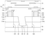
도 1은 본 발명의 몇몇 실시예들에 따른 반도체 장치를 설명하기 위한 개략적인 레이아웃도이다. 도 2는 도 1의 I - I를 따라서 절단한 단면도이다.1 is a schematic layout diagram illustrating a semiconductor device according to some embodiments of the inventive concept. FIG. 2 is a cross-sectional view taken along line I-I of FIG. 1 .
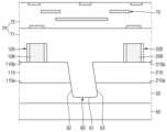
도 1 및 도 2를 참고하면, 본 발명의 몇몇 실시예들에 따른 반도체 장치(10)는 제1 소자 패턴(105)과, 제2 소자 패턴(205)과, 제1 반도체 기판 패턴(110)과, 제2 반도체 기판 패턴(210)과, 매립 절연막(55)과, 분리 트렌치(60)를 포함할 수 있다.1 and 2 , a
베이스 기판(50)은 서로 인접하는 제1 소자 영역(AREA 1)과, 제2 소자 영역(AREA 2)을 포함할 수 있다. 제1 소자 영역(AREA 1) 및 제2 소자 영역(AREA 2)은 분리 트렌치(60)에 의해 분리될 수 있다.The
베이스 기판(50)은 예를 들어, 실리콘(Si), 실리콘 게르마늄(SiGe), 안티몬화 인듐(InSb), 납 텔루르 화합물(PbTe), 인듐 비소(InAs), 인듐 인화물(InP), 갈륨 비소(GaAs), 안티몬화 갈륨(GaSb) 및 이들의 조합 중 하나를 포함할 수 있으나, 이에 한정되는 것은 아니다.The
본 발명의 몇몇 실시예들에 따른 반도체 장치에서, 베이스 기판(50)은 실리콘 기판인 것으로 설명한다.In the semiconductor device according to some embodiments of the present invention, the
매립 절연막(55)은 베이스 기판(50) 상에 형성될 수 있다. 매립 절연막(55)은 베이스 기판(50)과 접촉할 수 있다. 여기서, "접촉한다"는 것은 매립 절연막(55)과 베이스 기판(50) 사이에 삽입막이 형성되지 않음을 의미할 수 있다.The filling insulating
매립 절연막(55)은 절연 물질을 포함할 수 있다. 매립 절연막(55)을 예를 들어, 실리콘 산화물(SiO2)을 포함할 수 있다. 매립 절연막(55)은 제2 반도체 기판 패턴(210)과 베이스 기판(50)을 본딩시키는 접착막의 역할을 할 수 있다. 이에 관한 설명은 제조 방법을 통해 상술한다.The filling insulating
제1 반도체 기판 패턴(110)은 매립 절연막(55) 상에 형성될 수 있다. 제1 반도체 기판 패턴(110)은 매립 절연막(55)과 접촉할 수 있다.The first
제1 반도체 기판 패턴(110)은 제1 소자 영역(AREA 1)에 형성될 수 있다. 제1 소자 영역(AREA 1)은 제1 반도체 기판 패턴(110)에 의해 정의될 수 있다.The first
제1 반도체 기판 패턴(110)은 서로 마주보는 제1 면(110a)과, 제2 면(110b)을 포함할 수 있다. 제1 반도체 기판 패턴의 제1 면(110a)은 매립 절연막(55)과 마주볼 수 있다. 즉, 제1 반도체 기판 패턴의 제1 면(110a)은 매립 절연막(55)과 접촉할 수 있다.The first
제2 반도체 기판 패턴(210)은 매립 절연막(55) 상에 형성될 수 있다. 제2 반도체 기판 패턴(210)은 매립 절연막(55)과 접촉할 수 있다.The second
제2 반도체 기판 패턴(210)은 제2 소자 영역(AREA 2)에 형성될 수 있다. 제2 소자 영역(AREA 2)은 제2 반도체 기판 패턴(210)에 의해 정의될 수 있다. 제2 반도체 기판 패턴(210)은 제1 반도체 기판 패턴(110)과 이격되어 있다.The second
제2 반도체 기판 패턴(210)은 서로 마주보는 제1 면(210a)과, 제2 면(210b)을 포함할 수 있다. 제2 반도체 기판 패턴의 제1 면(210a)은 매립 절연막(55)과 마주볼 수 있다. 즉, 제2 반도체 기판 패턴의 제1 면(210a)은 매립 절연막(55)과 접촉할 수 있다.The second
예를 들어, 제1 반도체 기판 패턴(110)과 베이스 기판(50) 사이의 매립 절연막(55)의 두께(h11)는 제2 반도체 기판 패턴(210)과 베이스 기판(50) 사이의 매립 절연막(55)의 두께(h12)와 동일할 수 있다.For example, the thickness h11 of the insulating buried
각각의 제1 반도체 기판 패턴(110) 및 제2 반도체 기판 패턴(210)은 예를 들어, 원소 반도체 물질인 실리콘 또는 게르마늄을 포함할 수 있다. 또한, 각각의 제1 반도체 기판 패턴(110) 및 제2 반도체 기판 패턴(210)은 화합물 반도체를 포함할 수 있고, 예를 들어, IV-IV족 화합물 반도체 또는 III-V족 화합물 반도체를 포함할 수 있다.Each of the first
구체적으로, IV-IV족 화합물 반도체를 예로 들면, 각각의 제1 반도체 기판 패턴(110) 및 제2 반도체 기판 패턴(210)은 탄소(C), 규소(Si), 게르마늄(Ge), 주석(Sn) 중 적어도 2개 이상을 포함하는 이원계 화합물(binary compound), 삼원계 화합물(ternary compound) 또는 이들에 IV족 원소가 도핑된 화합물일 수 있다. III-V족 화합물 반도체를 예로 들면, 각각의 제1 반도체 기판 패턴(110) 및 제2 반도체 기판 패턴(210)은 III족 원소로 알루미늄(Al), 갈륨(Ga) 및 인듐(In) 중 적어도 하나와 V족 원소인 인(P), 비소(As) 및 안티모늄(Sb) 중 하나가 결합되어 형성되는 이원계 화합물, 삼원계 화합물 또는 사원계 화합물 중 하나일 수 있다.Specifically, taking a group IV-IV compound semiconductor as an example, each of the first
제1 반도체 기판 패턴(110) 및 제2 반도체 기판 패턴(210)은 동일한 물질을 포함할 수도 있고, 서로 다른 물질을 포함할 수도 있다. 또는, 제1 반도체 기판 패턴(110) 및 제2 반도체 기판 패턴(210)은 동일한 기판 상에 서로 다른 에피택셜막이 형성되어 있을 수도 있다.The first
제1 반도체 기판 패턴(110)의 두께는 제2 반도체 기판 패턴(210)의 두께와 동일할 수도 있고, 서로 다를 수도 있다. 또한, 베이스 기판(50)으로부터 제1 반도체 기판 패턴의 제2 면(110b)까지의 높이는 베이스 기판(50)으로부터 제2 반도체 기판 패턴의 제2 면(210b)까지의 높이와 동일할 수도 있고, 서로 다를 수도 있다.The thickness of the first
제1 소자 패턴(105)은 제1 반도체 기판 패턴(110) 상에 형성될 수 있다. 제1 소자 패턴(105)은 제1 반도체 기판 패턴의 제2 면(110b) 상에 형성될 수 있다. 제1 소자 패턴(105)은 제1 게이트 전극(106)을 포함할 수 있다. 예를 들어, 제1 소자 패턴(105)은 제1 트랜지스터를 포함할 수 있다.The
제2 소자 패턴(205)은 제2 반도체 기판 패턴(210) 상에 형성될 수 있다. 제2 소자 패턴(205)은 제2 반도체 기판 패턴의 제2 면(210b) 상에 형성될 수 있다. 제2 소자 패턴(205)은 제2 게이트 전극(206)을 포함할 수 있다. 예를 들어, 제2 소자 패턴(205)은 제2 트랜지스터를 포함할 수 있다.The
도 2에서, 제1 및 제2 소자 패턴(105, 205)의 형상, 즉 제1 및 제2 트랜지스터의 형상은 간략하게 도시되었을 뿐, 이에 제한되는 것은 아니다.In FIG. 2 , the shapes of the first and
즉, 제1 소자 패턴(105)은 제1 게이트 전극(106)과, 제1 트랜지스터의 소오스/드레인 영역과, 소오스/드레인 영역 사이의 제1 트랜지스터의 채널 영역을 포함할 수 있다. 마찬가지로, 제2 소자 패턴(205)은 제2 게이트 전극(206)과, 소오스/드레인 영역과, 소오스/드레인 영역 사이의 채널 영역을 포함할 수 있다.That is, the
본 발명의 몇몇 실시예들에 따른 반도체 장치에서, 각각의 제1 소자 패턴(105) 및 제2 소자 패턴(205)은 평면(planar) 트랜지스터, 핀형 패턴 형상의 채널 영역을 포함하는 핀형 트랜지스터(FinFET), 터널링 트랜지스터(tunneling FET), 나노 와이어 또는 나노 시트(sheet) 형상의 채널 영역을 포함하는 GAA(Gate-All-Around) 트랜지스터, 또는 채널 영역이 기판의 두께 방향으로 배열된 수직형(vertical) 트랜지스터 중의 하나를 포함할 수 있지만, 이에 제한되는 것은 아니다. 즉, 트랜지스터의 형태가 상술한 종류에 한정되는 것은 아니다.In the semiconductor device according to some embodiments of the present invention, each of the
제1 소자 패턴(105)의 형상 및 제2 소자 패턴(205)의 형상은 서로 다를 수 있다. 예를 들어, 제1 트랜지스터의 채널 영역의 모양은 제2 트랜지스터의 채널 영역의 모양과 다를 수 있다.The shape of the
제1 트랜지스터의 채널 영역은 핀형 패턴 형상이고, 제2 트랜지스터의 채널 영역은 나노 와이어 형상일 경우, 제1 트랜지스터의 채널 영역의 모양은 제2 트랜지스터의 채널 영역의 모양과 다르다고 할 수 있다.When the channel region of the first transistor has a fin-shaped pattern shape and the channel region of the second transistor has a nanowire shape, the shape of the channel region of the first transistor may be different from that of the second transistor.
이 때, 제1 트랜지스터의 채널 영역의 물질은 제2 트랜지스터의 채널 영역의 물질과 동일할 수도 있고, 서로 다를 수도 있다.In this case, the material of the channel region of the first transistor may be the same as or different from that of the channel region of the second transistor.
제1 소자 패턴(105)의 형상 및 제2 소자 패턴(205)의 형상이 동일해도, 제1 트랜지스터의 채널 영역의 물질 및 제2 트랜지스터의 채널 영역의 물질을 서로 다를 수 있다.Even if the shape of the
제1 트랜지스터의 채널 영역 및 제2 트랜지스터의 채널 영역이 핀형 패턴 형상이고, 제1 트랜지스터의 채널 영역의 물질은 실리콘 또는 실리콘 게르마늄을 포함하고, 제2 트랜지스터의 채널 영역의 물질은 III-V 화합물 반도체를 포함할 경우, 제1 소자 패턴(105)의 형상 및 제2 소자 패턴(205)의 형상이 동일해도, 제1 트랜지스터의 채널 영역의 물질 및 제2 트랜지스터의 채널 영역의 물질을 서로 다를 수 있다.The channel region of the first transistor and the channel region of the second transistor have a fin-shaped pattern, the material of the channel region of the first transistor includes silicon or silicon germanium, and the material of the channel region of the second transistor is a III-V compound semiconductor. , even if the shape of the
도 2에서, 베이스 기판(50)으로부터 제1 게이트 전극(106)의 상면까지의 높이(h21)는 베이스 기판(50)으로부터 제2 게이트 전극(206)의 상면까지의 높이(h22)와 동일한 것으로 도시하였지만, 설명의 편의를 위한 것일 뿐, 이에 제한되는 것은 아니다.2, the height h21 from the
또한, 도 2에서, 제1 트랜지스터의 소오스/드레인 영역 사이의 제1 게이트 전극(106)의 폭은 제2 트랜지스터의 소오스/드레인 영역 사이의 제2 게이트 전극(206)의 폭과 동일한 것으로 도시하였지만, 설명의 편의를 위한 것일 뿐, 이에 제한되는 것은 아니다.2, the width of the
분리 트렌치(60)는 제1 반도체 기판 패턴(110)과 제2 반도체 기판 패턴(210) 사이에 형성될 수 있다. 또한, 분리 트렌치(60)는 매립 절연막(55) 내에 형성될 수 있다. 제1 반도체 기판 패턴(110) 및 제2 반도체 기판 패턴(210)은 분리 트렌치(60)에 의해 구분될 수 있다.The
분리 트렌치(60)는 서로 마주보는 제1 측벽(62) 및 제2 측벽(63)을 포함할 수 있다. 분리 트렌치(60)은 분리 트렌치의 제1 측벽(62) 및 분리 트렌치의 제2 측벽(63)을 연결하는 바닥면(61)을 포함할 수 있다.The
분리 트렌치의 제1 측벽(62)은 제1 반도체 기판 패턴(110) 및 매립 절연막(55)에 의해 정의될 수 있다. 분리 트렌치의 제2 측벽(63)은 제2 반도체 기판 패턴(210) 및 매립 절연막(55)에 의해 정의될 수 있다. 분리 트렌치의 바닥면(61)은 매립 절연막(55)에 의해 정의될 수 있다.The
분리 트렌치의 제1 측벽(62)과, 분리 트렌치의 바닥면(61)의 연결 부분은 라운딩되어 있을 수 있다. 하지만, 분리 트렌치의 제2 측벽(63)과, 분리 트렌치의 바닥면(61)의 연결 부분은 라운딩되지 않을 수 있다. 즉, 하지만, 분리 트렌치의 제2 측벽(63)과, 분리 트렌치의 바닥면(61)의 연결 부분은 각진 형상을 가질 수 있다.A connection portion between the
좀 더 구체적으로, 매립 절연막(55)에 의해 정의되는 분리 트렌치의 제1 측벽(62)의 일부와, 분리 트렌치의 바닥면(61) 사이의 연결 부분은 라운딩되어 있을 수 있다. 매립 절연막(55)에 의해 정의되는 분리 트렌치의 제2 측벽(63)의 일부와, 분리 트렌치의 바닥면(61) 사이의 연결 부분은 라운딩되지 않을 수 있다.More specifically, a connection portion between a portion of the
제1 반도체 기판 패턴(110)에 의해 정의되는 분리 트렌치의 제1 측벽(62)과, 매립 절연막(55)에 의해 정의되는 분리 트렌치의 제1 측벽(62)은 연속일 수 있다. 또한, 제2 반도체 기판 패턴(210)에 의해 정의되는 분리 트렌치의 제2 측벽(63)과, 매립 절연막(55)에 의해 정의되는 분리 트렌치의 제2 측벽(63)은 연속일 수 있다.The
여기에서, "측벽이 연속된다"는 의미는 제1 반도체 기판 패턴(110)에 의해 정의되는 분리 트렌치의 제1 측벽(62)과, 매립 절연막(55)에 의해 정의되는 분리 트렌치의 제1 측벽(62) 사이에, 돌출된 부분이 없음을 의미한다.Here, "continuous sidewalls" means the
즉, 제1 반도체 기판 패턴(110)에 의해 정의되는 분리 트렌치의 제1 측벽(62)과, 매립 절연막(55)에 의해 정의되는 분리 트렌치의 제1 측벽(62) 사이에, 제1 및 제2 반도체 기판 패턴의 제1 면(110a, 210a)과 접촉하는 매립 절연막(55)의 상면으로 이루어진 단차가 없을 수 있다.That is, between the
분리 트렌치의 제1 측벽(62) 및 분리 트렌치의 제2 측벽(63)은 동일한 방향으로 기울어져 있을 수 있다. 예를 들어, 분리 트렌치의 제1 측벽(62)은 분리 트렌치의 바닥면(61)과 둔각을 이룰 수 있고, 분리 트렌치의 제2 측벽(63)은 분리 트렌치의 바닥면(61)과 예각을 이룰 수 있다.The
또한, 제1 반도체 기판 패턴의 제1 면(110a)과, 제1 반도체 기판 패턴(110)에 의해 정의되는 분리 트렌치의 제1 측벽(62)은 예각을 이룰 수 있다. 반면, 제2 반도체 기판 패턴의 제1 면(210a)과, 제2 반도체 기판 패턴(210)에 의해 정의되는 분리 트렌치의 제2 측벽(63)은 둔각을 이룰 수 있다.Also, the
도 2에서, 제1 반도체 기판 패턴(110)에 의해 정의되는 분리 트렌치의 제1 측벽(62)과, 매립 절연막(55)에 의해 정의되는 분리 트렌치의 제1 측벽(62)은 동일한 기울기를 갖고, 제2 반도체 기판 패턴(210)에 의해 정의되는 분리 트렌치의 제2 측벽(63)과, 매립 절연막(55)에 의해 정의되는 분리 트렌치의 제2 측벽(63)은 동일한 기울기를 갖는 것으로 도시하였지만, 설명의 편의를 위한 것일 뿐, 이에 제한되는 것은 아니다.In FIG. 2 , the
제1 층간 절연막(70)은 제1 반도체 기판 패턴(110) 및 제2 반도체 기판 패턴(210) 상에 형성될 수 있다. 제1 층간 절연막(70)은 제1 하부 층간 절연막(71)과, 제1 상부 층간 절연막(72)을 포함할 수 있다. 제1 하부 층간 절연막(71)은 제1 소자 패턴(105) 및 제2 소자 패턴(205)을 덮을 수 있다. 제1 하부 층간 절연막(71)은 분리 트렌치(60)를 채울 수 있다. 제1 상부 층간 절연막(72)은 제1 하부 층간 절연막(71) 상에 형성될 수 있다.The first
제1 하부 층간 절연막(71) 및 제1 상부 층간 절연막(72)은 각각 예를 들어, 실리콘 산화물, 실리콘 질화물, 실리콘 산질화물, FOX(Flowable Oxide), TOSZ(Tonen SilaZene), USG(Undoped Silica Glass), BSG(Borosilica Glass), PSG(PhosphoSilica Glass), BPSG(BoroPhosphoSilica Glass), PETEOS(Plasma Enhanced Tetra Ethyl Ortho Silicate), FSG(Fluoride Silicate Glass), CDO(Carbon Doped silicon Oxide), Xerogel, Aerogel, Amorphous Fluorinated Carbon, OSG(Organo Silicate Glass), Parylene, BCB(bis-benzocyclobutenes), SiLK, polyimide, porous polymeric material 또는 이들의 조합을 포함할 수 있으나, 이에 제한되는 것은 아니다.The first lower
제1 통합(integration) 연결 배선(75)은 제1 상부 층간 절연막(72) 내에 형성될 수 있다. 제1 통합 연결 배선(75)은 제1 소자 패턴(105) 및 제2 소자 패턴(205)과 전기적으로 연결될 수 있다. 즉, 제1 통합 연결 배선(75)은 제1 소자 패턴(105)과 제2 소자 패턴(205)을 전기적으로 연결할 수 있다. 제1 통합 연결 배선(75) 중의 일부는 분리 트렌치(60)를 가로질러 형성될 수 있다.A first
기판 접합 기술을 이용하여, 하나의 베이스 기판(50) 상에 서로 다른 특성을 갖는 제1 및 제2 소자 패턴(205)를 구현함으로써, 반도체 장치의 밀도를 향상시킬 수 있다.Density of the semiconductor device may be improved by implementing the first and
또한, 제1 소자 패턴(105) 및 제2 소자 패턴(205)은 별도의 제조 공정을 통해서 형성된다. 제1 소자 패턴(105)의 제조 공정이 제2 소자 패턴(205)의 제조 공정의 공정 제한 요소로 작용하지 않기 때문에, 제1 소자 패턴(105) 및 제2 소자 패턴(205)은 최적화된 퍼포먼스(performance)를 보여줄 수 있다. 따라서, 반도체 장치의 소자 특성을 개선할 수 있다.In addition, the
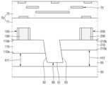
도 3 내지 도 6은 각각 본 발명의 몇몇 실시예들에 따른 반도체 장치를 설명하기 위한 도면이다. 설명의 편의상, 도 2에 대한 설명과 다른 점을 중심으로 설명한다.3 to 6 are diagrams for describing a semiconductor device according to some example embodiments of the inventive concept. For convenience of description, the description will focus on points different from the description of FIG. 2 .
도 3을 참고하면, 본 발명의 몇몇 실시예들에 따른 반도체 장치에서, 분리 트렌치의 제1 측벽(62)과, 분리 트렌치의 바닥면(61)의 연결 부분은 라운딩되지 않을 수 있다.Referring to FIG. 3 , in the semiconductor device according to some example embodiments, a connection portion between the
매립 절연막(55)에 의해 정의되는 분리 트렌치의 제1 측벽(62)의 일부와, 분리 트렌치의 바닥면(61) 사이의 연결 부분은 라운딩되지 않을 수 있다. 즉, 분리 트렌치의 제1 측벽(62)과, 분리 트렌치의 바닥면(61)의 연결 부분은 각진 형상을 가질 수 있다.A connection portion between a portion of the
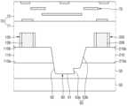
도 4를 참고하면, 본 발명의 몇몇 실시예들에 따른 반도체 장치에서, 분리 트렌치의 제2 측벽(63)과, 분리 트렌치의 바닥면(61)의 연결 부분은 라운딩되어 있을 수 있다.Referring to FIG. 4 , in the semiconductor device according to some example embodiments, a connection portion between the
매립 절연막(55)에 의해 정의되는 분리 트렌치의 제2 측벽(63)의 일부와, 분리 트렌치의 바닥면(61) 사이의 연결 부분은 라운딩되어 있을 수 있다. 제2 반도체 기판 패턴(210)을 베이스 기판(50)에 접합하는 공정 중, 분리 트렌치의 제2 측벽(63)과, 분리 트렌치의 바닥면(61)의 연결 부분은 라운딩될 수 있다.A connection portion between a portion of the
좀 더 구체적으로, 분리 트렌치의 제2 측벽(63)의 일부를 정의하는 매립 절연막(55) 부분과, 분리 트렌치의 바닥면(61)을 정의하는 매립 절연막(55) 부분이 접합되는 동안, 분리 트렌치의 제2 측벽(63)과, 분리 트렌치의 바닥면(61)의 연결 부분은 라운딩될 수 있다.More specifically, while the portion of the insulating buried
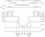
도 5를 참고하면, 본 발명의 몇몇 실시예들에 따른 반도체 장치에서, 분리 트렌치의 제1 측벽(62)과 분리 트렌치의 바닥면(61) 사이의 각은 직각일 수 있다.Referring to FIG. 5 , in a semiconductor device according to some example embodiments, an angle between a
분리 트렌치의 제2 측벽(63)과 분리 트렌치의 바닥면(61) 사이의 각은 직각일 수 있다.An angle between the
또한, 제1 반도체 기판 패턴의 제1 면(110a)과, 제1 반도체 기판 패턴(110)에 의해 정의되는 분리 트렌치의 제1 측벽(62)은 직각을 이루고, 제2 반도체 기판 패턴의 제1 면(210a)과, 제2 반도체 기판 패턴(210)에 의해 정의되는 분리 트렌치의 제2 측벽(63)은 직각을 이룰 수 있다.In addition, the
도 6을 참고하면, 본 발명의 몇몇 실시예들에 따른 반도체 장치에서, 제1 반도체 기판 패턴(110)과 베이스 기판(50) 사이의 매립 절연막(55)의 두께(h11)는 제2 반도체 기판 패턴(210)과 베이스 기판(50) 사이의 매립 절연막(55)의 두께(h12)와 다를 수 있다.Referring to FIG. 6 , in the semiconductor device according to some embodiments of the present invention, the thickness h11 of the filling insulating
일 예로, 제1 반도체 기판 패턴(110)과 베이스 기판(50) 사이의 매립 절연막(55)의 두께(h11)는 제2 반도체 기판 패턴(210)과 베이스 기판(50) 사이의 매립 절연막(55)의 두께(h12)보다 클 수 있다.For example, the thickness h11 of the insulating buried
다른 예로, 제1 반도체 기판 패턴(110)과 베이스 기판(50) 사이의 매립 절연막(55)의 두께(h11)는 제2 반도체 기판 패턴(210)과 베이스 기판(50) 사이의 매립 절연막(55)의 두께(h12)보다 작을 수 있다.As another example, the thickness h11 of the insulating buried
제2 반도체 기판 패턴(210)을 베이스 기판(50)에 접합시키기 위한 실리콘 산화막의 두께에 따라, 제2 반도체 기판 패턴(210)과 베이스 기판(50) 사이의 매립 절연막(55)의 두께(h12)는 변할 수 있기 때문이다.Depending on the thickness of the silicon oxide film for bonding the second
도 7은 본 발명의 몇몇 실시예들에 따른 반도체 장치를 설명하기 위한 도면이다. 설명의 편의상, 도 2에 대한 설명과 다른 점을 중심으로 설명한다.7 is a diagram for describing a semiconductor device according to some embodiments of the inventive concept. For convenience of description, the description will focus on points different from the description of FIG. 2 .
도 7을 참고하면, 본 발명의 몇몇 실시예들에 따른 반도체 장치에서, 분리 트렌치의 제1 측벽(62)은 제1 부분(62a)과, 제2 부분(62b)를 포함할 수 있다.Referring to FIG. 7 , in a semiconductor device according to some example embodiments, a
분리 트렌치의 제1 측벽의 제1 부분(62a) 및 분리 트렌치의 제1 측벽의 제2 부분(62b)은 분리 트렌치의 바닥면(61)에 대해 둔각인 기울기를 가질 수 있다.The
분리 트렌치의 제1 측벽(62)은 분리 트렌치의 제1 측벽의 제1 부분(62a)과 분리 트렌치의 제1 측벽의 제2 부분(62b)을 연결하는 연결부를 포함할 수 있다. 분리 트렌치의 제1 측벽(62)의 연결부는 베이스 기판(50)과 나란한 방향으로 연장되는 부분일 수 있다.The
도 7에서, 분리 트렌치의 제1 측벽(62)의 연결부는 매립 절연막(55)에 의해 정의되는 것으로 도시하였지만, 이에 제한되는 것은 아니다. 즉, 분리 트렌치의 제1 측벽의 제2 부분(62b)을 형성하는 공정에서, 제1 반도체 기판 패턴(110)의 제거되는 양에 따라 달라질 수 있다.In FIG. 7 , the connection portion of the
도 8은 본 발명의 몇몇 실시예들에 따른 반도체 장치를 설명하기 위한 도면이다. 설명의 편의상, 도 2에 대한 설명과 다른 점을 중심으로 설명한다.8 is a diagram for describing a semiconductor device according to some example embodiments of the inventive concepts. For convenience of description, the description will focus on points different from the description of FIG. 2 .
도 8을 참고하면, 본 발명의 몇몇 실시예들에 따른 반도체 장치에서, 분리 트렌치의 제2 측벽(63)은 제1 부분(63a)과, 제2 부분(63b)를 포함할 수 있다.Referring to FIG. 8 , in a semiconductor device according to some example embodiments, the
분리 트렌치의 제2 측벽의 제1 부분(63a)은 분리 트렌치의 바닥면(61)에 대해 예각을 갖는 부분일 수 있다. 분리 트렌치의 제2 측벽의 제2 부분(63b)은 분리 트렌치의 바닥면(61)에 대해 둔각을 갖는 부분일 수 있다.The
즉, 분리 트렌치의 제2 측벽(63)은 분리 트렌치의 바닥면(61)에 대해 둔각을 이루는 부분(63b)와, 예각을 이루는 부분(63a)을 포함할 수 있다.That is, the
분리 트렌치의 제2 측벽(63)은 예를 들어, 두 번의 식각 공정에 의해 형성될 수 있다. 즉, 분리 트렌치의 제2 측벽의 제1 부분(63a)을 형성하는 공정과, 분리 트렌치의 제2 측벽의 제2 부분(63b)을 형성하는 공정은 서로 다른 식각 공정일 수 있다.The
예를 들어, 분리 트렌치의 제2 측벽의 제1 부분(63a)은 매립 절연막(55)에 의해 정의되고, 분리 트렌치의 제2 측벽의 제2 부분(63b)은 매립 절연막(55) 및 제2 반도체 기판 패턴(210)에 의해 정의될 수 있다.For example, the
도 8에서, 제2 반도체 기판 패턴의 제1 면(210a)과, 제2 반도체 기판 패턴(210)에 의해 정의되는 분리 트렌치의 제2 측벽(63)의 적어도 일부는 예각을 이룰 수 있다. 즉, 제2 반도체 기판 패턴의 제1 면(210a)과, 제2 반도체 기판 패턴(210)에 의해 정의되는 분리 트렌치의 제2 측벽의 제2 부분(63b)은 예각을 이룰 수 있다.In FIG. 8 , the
도 9 내지 도 11은 각각 본 발명의 몇몇 실시예들에 따른 반도체 장치를 설명하기 위한 도면이다. 설명의 편의상, 도 8에 대한 설명과 다른 점을 중심으로 설명한다.9 to 11 are diagrams for describing a semiconductor device according to some example embodiments of the inventive concept. For convenience of description, the description will focus on differences from the description of FIG. 8 .
도 9를 참고하면, 본 발명의 몇몇 실시예들에 따른 반도체 장치에서, 분리 트렌치의 제2 측벽의 제1 부분(63a)은 매립 절연막(55) 및 제2 반도체 기판 패턴(210)에 의해 정의될 수 있다. 분리 트렌치의 제2 측벽의 제2 부분(63b)은 제2 반도체 기판 패턴(210)에 의해 정의될 수 있다.Referring to FIG. 9 , in a semiconductor device according to some example embodiments, a
제2 반도체 기판 패턴의 제1 면(210a)과, 제2 반도체 기판 패턴(210)에 의해 정의되는 분리 트렌치의 제2 측벽(63)의 적어도 일부는 둔각을 이룰 수 있다. 제2 반도체 기판 패턴의 제1 면(210a)과, 제2 반도체 기판 패턴(210)에 의해 정의되는 분리 트렌치의 제2 측벽의 제1 부분(63a)은 둔각을 이룰 수 있다.The
도 10을 참고하면, 본 발명의 몇몇 실시예들에 따른 반도체 장치에서, 분리 트렌치의 제2 측벽(63)은 분리 트렌치의 제2 측벽의 제1 부분(63a)과 분리 트렌치의 제2 측벽의 제2 부분(63b)을 연결하는 연결부를 포함할 수 있다.Referring to FIG. 10 , in a semiconductor device according to some embodiments of the present disclosure, the
분리 트렌치의 제2 측벽(63)의 연결부는 베이스 기판(50)과 나란한 방향으로 연장되는 부분일 수 있다. 분리 트렌치의 제2 측벽(63)의 연결부는 매립 절연막(55)에 의해 정의될 수 있다.The connection portion of the
분리 트렌치의 제2 측벽의 제2 부분(63b)과, 분리 트렌치의 제2 측벽(63)의 연결부의 연결 부분은 라운딩되어 있을 수 있다. 하지만, 분리 트렌치의 제2 측벽의 제1 부분(63a)과, 분리 트렌치의 제2 측벽(63)의 연결부의 연결 부분은 라운딩되지 않을 수 있다.A connection portion between the
제2 반도체 기판 패턴의 제1 면(210a)과, 제2 반도체 기판 패턴(210)에 의해 정의되는 분리 트렌치의 제2 측벽(63)의 적어도 일부는 예각을 이룰 수 있다. 제2 반도체 기판 패턴의 제1 면(210a)과, 제2 반도체 기판 패턴(210)에 의해 정의되는 분리 트렌치의 제2 측벽의 제2 부분(63b)은 예각을 이룰 수 있다.The
도 11을 참고하면, 본 발명의 몇몇 실시예들에 따른 반도체 장치에서, 분리 트렌치의 제2 측벽(63)은 분리 트렌치의 제2 측벽의 제1 부분(63a)과 분리 트렌치의 제2 측벽의 제2 부분(63b)을 연결하는 연결부를 포함할 수 있다.Referring to FIG. 11 , in the semiconductor device according to some embodiments of the present disclosure, the
분리 트렌치의 제2 측벽의 제1 부분(63a)은 매립 절연막(55) 및 제2 반도체 기판 패턴(210)에 의해 정의될 수 있다. 분리 트렌치의 제2 측벽의 제2 부분(63b)은 제2 반도체 기판 패턴(210)에 의해 정의될 수 있다.The
분리 트렌치의 제2 측벽(63)의 연결부는 제2 반도체 기판 패턴의 제1 면(210a)과 나란한 방향으로 연장되는 부분일 수 있다. 분리 트렌치의 제2 측벽(63)의 연결부는 제2 반도체 기판 패턴(210)에 의해 정의될 수 있다.The connection portion of the
분리 트렌치의 제2 측벽의 제2 부분(63b)과, 분리 트렌치의 제2 측벽(63)의 연결부의 연결 부분은 라운딩되어 있을 수 있다. 하지만, 분리 트렌치의 제2 측벽의 제1 부분(63a)과, 분리 트렌치의 제2 측벽(63)의 연결부의 연결 부분은 라운딩되지 않을 수 있다.A connection portion between the
제2 반도체 기판 패턴의 제1 면(210a)과, 제2 반도체 기판 패턴(210)에 의해 정의되는 분리 트렌치의 제2 측벽(63)의 적어도 일부는 둔각을 이룰 수 있다. 제2 반도체 기판 패턴의 제1 면(210a)과, 제2 반도체 기판 패턴(210)에 의해 정의되는 분리 트렌치의 제2 측벽의 제1 부분(63a)은 둔각을 이룰 수 있다.The
도 12는 본 발명의 몇몇 실시예들에 따른 반도체 장치를 설명하기 위한 도면이다. 설명의 편의상, 도 5를 이용하여 설명한 것과 다른 점을 중심으로 설명한다.12 is a diagram for describing a semiconductor device according to some example embodiments. For convenience of description, the description will focus on points different from those described with reference to FIG. 5 .
도 12를 참고하면, 본 발명의 몇몇 실시예들에 따른 반도체 장치에서, 분리 트렌치의 제1 측벽(62)은 제1 부분(62a)과, 제2 부분(62b)을 포함할 수 있다. 분리 트렌치의 제2 측벽(63)은 제1 부분(63a)과, 제2 부분(63b)을 포함할 수 있다.Referring to FIG. 12 , in a semiconductor device according to some example embodiments, a
분리 트렌치의 제1 측벽(62)은 분리 트렌치의 제1 측벽의 제1 부분(62a)과 분리 트렌치의 제1 측벽의 제2 부분(62b)을 연결하는 연결부를 포함할 수 있다. 분리 트렌치의 제2 측벽(63)은 분리 트렌치의 제2 측벽의 제1 부분(63a)과 분리 트렌치의 제2 측벽의 제2 부분(63b)을 연결하는 연결부를 포함할 수 있다.The
도 12에서, 분리 트렌치의 제1 측벽(62)의 연결부 및 분리 트렌치의 제2 측벽(63)의 연결부는 매립 절연막(55)에 의해 정의되는 것으로 도시하였지만, 이에 제한되는 것은 아니다.In FIG. 12 , the connection portion of the
도 12에서 도시된 것과 달리, 분리 트렌치의 제1 측벽(62) 및 분리 트렌치의 제2 측벽(63) 중 하나만 연결부를 포함할 수 있음은 물론이다.Unlike that shown in FIG. 12 , only one of the
도 13 내지 도 15는 각각 본 발명의 몇몇 실시예들에 따른 반도체 장치를 설명하기 위한 도면이다. 설명의 편의상, 도 1 및 도 2에 대한 설명과 다른 점을 중심으로 설명한다.13 to 15 are diagrams for describing a semiconductor device according to some example embodiments of the inventive concept. For convenience of description, the description will focus on points different from those of FIGS. 1 and 2 .
도 13을 참고하면, 본 발명의 몇몇 실시예들에 따른 반도체 장치는 제1 식각 정지막(120) 및 제2 식각 정지막(220)을 더 포함할 수 있다.Referring to FIG. 13 , a semiconductor device according to some example embodiments may further include a first
제1 식각 정지막(120)은 제1 반도체 기판 패턴(110) 상의 제1 소자 패턴(105)의 적어도 일부를 따라 연장될 수 있다. 제1 식각 정지막(120)은 제1 반도체 기판 패턴의 제2 면(110b) 상에도 형성될 수 있다.The first
제2 식각 정지막(220)은 제2 반도체 기판 패턴(210) 상의 제2 소자 패턴(205)의 적어도 일부를 따라 연장될 수 있다. 제2 식각 정지막(220)은 제2 반도체 기판 패턴의 제2 면(210b) 상에도 형성될 수 있다.The second
제1 식각 정지막(120) 및 제2 식각 정지막(220)은 서로 간에 이격되어 있다. 제1 식각 정지막(120) 및 제2 식각 정지막(220)을 사이에 두고, 분리 트렌치(60)가 형성될 수 있다. 즉, 제1 식각 정지막(120)의 일단과, 제2 식각 정지막(220)의 일단 사이에, 분리 트렌치(60)가 배치될 수 있다.The first
제1 반도체 기판 패턴(110) 상의 제1 하부 층간 절연막(71)은 제1 식각 정지막(120) 상에 형성될 수 있다. 제2 반도체 기판 패턴(210) 상의 제1 하부 층간 절연막(71)은 제2 식각 정지막(220) 상에 형성될 수 있다.The first lower
제1 식각 정지막(120) 및 제2 식각 정지막(220)은 제1 하부 층간 절연막(71)에 대해 식각 선택비를 갖는 물질을 포함할 수 있다. 제1 식각 정지막(120) 및 제2 식각 정지막(220)은 각각 예를 들어, 실리콘 질화물, 실리콘 산질화물, 실리콘 탄화질화물 및 이들의 조합 중 하나를 포함할 수 있지만, 이에 제한되는 것은 아니다.The first
도 13에서, 제1 식각 정지막(120) 및 제2 식각 정지막(220)은 각각 분리 트렌치의 측벽(62, 63) 및 분리 트렌치의 바닥면(61)을 따라 연장되지 않는 것으로 도시하였지만, 이에 제한되는 것은 아니다. 즉, 제조 공정 중 제1 식각 정지막(120) 및 제2 식각 정지막(220)을 언제 형성하느냐에 따라, 제1 식각 정지막(120) 및/또는 제2 식각 정지막(220)의 일부는 분리 트렌치의 측벽(62, 63) 및 분리 트렌치의 바닥면(61) 상에 형성될 수도 있다.In FIG. 13 , the first
도 14를 참고하면, 본 발명의 몇몇 실시예들에 따른 반도체 장치는 제1 연결 배선(130)과, 제2 연결 배선(230)을 포함할 수 있다.Referring to FIG. 14 , a semiconductor device according to some example embodiments may include a
제1 연결 배선(130)은 제1 반도체 기판 패턴(110)과 중첩되는 제1 하부 층간 절연막(71) 내에 형성될 수 있다. 제1 연결 배선(130)은 제1 소자 패턴(105)과 전기적으로 연결될 수 있다. 제1 연결 배선(130)은 분리 트렌치(60)와 중첩되는 부분을 포함하지 않을 수 있다.The
제2 연결 배선(230)은 제2 반도체 기판 패턴(210)과 중첩되는 제1 하부 층간 절연막(71) 내에 형성될 수 있다. 제2 연결 배선(230)은 제2 소자 패턴(205)과 전기적으로 연결될 수 있다. 제2 연결 배선(230)은 분리 트렌치(60)와 중첩되는 부분을 포함하지 않을 수 있다.The
제1 연결 배선(130) 및 제2 연결 배선(230)은 제1 통합 연결 배선(75)을 통해 전기적으로 연결될 수 있다. 즉, 제1 연결 배선(130) 및 제2 연결 배선(230)은 직접적으로 연결되지 않을 수 있다.The
도 14에서, 베이스 기판(50)으로부터 제1 연결 배선(130) 중 가장 하부에 위치하는 배선까지의 높이(h31)는 베이스 기판(50)으로부터 제2 연결 배선(230) 중 가장 하부에 위치하는 배선까지의 높이(h32)와 실질적으로 동일한 것으로 도시하였지만, 이에 제한되는 것은 아니다.In FIG. 14 , the height h31 from the
제1 연결 배선(130) 및 제2 연결 배선(230)은 서로 다른 제조 공정을 통해 형성되므로, 베이스 기판(50)을 기준으로 제1 연결 배선(130)이 형성되는 레벨은 제2 연결 배선(230)이 형성되는 레벨과 다를 수 있다.Since the
도 15를 참고하면, 본 발명의 몇몇 실시예들에 따른 반도체 장치는 절연 라이너(65)를 포함할 수 있다.Referring to FIG. 15 , a semiconductor device according to some example embodiments may include an insulating
절연 라이너(65)는 분리 트렌치의 제1 측벽(62), 분리 트렌치의 바닥면(61) 및 분리 트렌치의 제2 측벽(63)을 따라 형성될 수 있다. 절연 라이너(65)는 제1 하부 층간 절연막(71)과 식각 선택비를 갖는 물질을 포함할 수 있다. 절연 라이너(65)는 예를 들어, 실리콘 질화물, 실리콘 산질화물 등을 포함할 수 있지만, 이에 제한되는 것은 아니다.The insulating
절연 라이너(65)는 분리 트렌치(60)를 채우는 제1 하부 층간 절연막(71)을 형성하기 전에 형성될 수 있으므로, 절연 라이너(65)는 제1 하부 층간 절연막(71)의 상면까지 연장될 수 있지만, 이에 제한되는 것은 아니다. 또한, 절연 라이너(65)는 제1 반도체 기판 패턴의 제2 면(110b) 및 제2 반도체 기판 패턴의 제2 면(210b)을 따라 연장되지 않을 수 있다.Since the insulating
제1 하부 층간 절연막(71) 중 분리 트렌치(60)를 채우는 제1 하부 층간 절연막(71)은 절연 라이너(65) 상에 형성될 수 있다.The first lower
도 16 및 도 17은 각각 본 발명의 몇몇 실시예들에 따른 반도체 장치를 설명하기 위한 도면이다. 설명의 편의상, 도 2에 대한 설명과 다른 점을 중심으로 설명한다.16 and 17 are diagrams for describing a semiconductor device according to some example embodiments of the inventive concepts. For convenience of description, the description will focus on points different from the description of FIG. 2 .
도 16을 참고하면, 본 발명의 몇몇 실시예들에 따른 반도체 장치는 제3 반도체 기판 패턴(310)과, 제1 삽입 매립 절연막(315)과, 제3 소자 패턴(305)과, 제2 통합 연결 배선(85)을 더 포함할 수 있다.Referring to FIG. 16 , a semiconductor device according to some embodiments of the present invention includes a third
제1 삽입 매립 절연막(315)은 제1 층간 절연막(70) 상에 배치될 수 있다. 제1 삽입 매립 절연막(315)은 예를 들어, 실리콘 산화물을 포함할 수 있지만, 이에 제한되는 것은 아니다.The first interstitial insulating layer 315 may be disposed on the first
제3 반도체 기판 패턴(310)은 제1 삽입 매립 절연막(315) 상에 형성될 수 있다. 제3 반도체 기판 패턴(310)은 제1 삽입 매립 절연막(315)과 접촉할 수 있다. 제3 반도체 기판 패턴(310)은 서로 마주보는 제1 면(310a)과, 제2 면(310b)을 포함할 수 있다. 제3 반도체 기판 패턴의 제1 면(310a)은 제1 삽입 매립 절연막(315) 및 제1 층간 절연막(70)과 마주볼 수 있다. 즉, 제3 반도체 기판 패턴의 제1 면(310a)은 제1 매립 절연막(55)과 접촉할 수 있다.The third
제3 반도체 기판 패턴(310)은 예를 들어, 원소 반도체 물질인 실리콘 또는 게르마늄을 포함하거나, IV-IV족 화합물 반도체 또는 III-V족 화합물 반도체를 포함할 수 있다.The third
제3 소자 패턴(305)은 제3 반도체 기판 패턴(310) 상에 형성될 수 있다. 제3 소자 패턴(305)은 제3 반도체 기판 패턴의 제2 면(310b) 상에 형성될 수 있다. 제3 소자 패턴(305)은 제3 게이트 전극(306)을 포함할 수 있다. 예를 들어, 제3 소자 패턴(305)은 제3 트랜지스터를 포함할 수 있다. 제3 소자 패턴(305)은 제3 게이트 전극(306)과, 제3 트랜지스터의 소오스/드레인 영역과, 소오스/드레인 영역 사이의 제3 트랜지스터의 채널 영역을 포함할 수 있다.The
도 16에서, 제3 소자 패턴(305)의 형상, 즉 제3 트랜지스터의 형상은 간략하게 도시되었을 뿐, 이에 제한되는 것은 아니다.In FIG. 16 , the shape of the
제3 소자 패턴(305)의 형상은 제1 소자 패턴(105)의 형상 및/또는 제2 소자 패턴(205)의 형상과 다를 수 있다. 또는, 제3 트랜지스터의 채널 영역의 물질은 제1 트랜지스터의 채널 영역의 물질 및/또는 제2 트랜지스터의 채널 영역의 물질과 다를 수 있다.The shape of the
도 16에서, 제3 반도체 기판 패턴(310)은 제1 반도체 기판 패턴(110) 및 제2 반도체 기판 패턴(210)에 걸쳐서 형성되는 것으로 도시하였지만, 이에 제한되는 것은 아니다.In FIG. 16 , the third
제1 층간 절연막(70) 상에 제3 반도체 기판 패턴(310)과 제3 소자 패턴(305)이 순차적으로 형성될 수 있다.A third
제2 층간 절연막(80)은 제3 반도체 기판 패턴(310) 상에 형성될 수 있다. 제2 층간 절연막(80)은 제2 하부 층간 절연막(81)과, 제2 상부 층간 절연막(82)을 포함할 수 있다. 제2 하부 층간 절연막(81)은 제3 소자 패턴(305)을 덮을 수 있다. 제2 상부 층간 절연막(82)은 제2 하부 층간 절연막(81) 상에 형성될 수 있다.The second
제2 통합 연결 배선(85)은 제2 상부 층간 절연막(82) 내에 형성될 수 있다. 제2 통합 연결 배선(85)은 제3 소자 패턴(305)과 전기적으로 연결될 수 있다.The second
제2 통합 연결 배선(85)은 관통 전극(87)에 의해 제1 통합 연결 배선(75)과 전기적으로 연결될 수 있다. 관통 전극(87)은 제1 삽입 매립 절연막(315), 제3 반도체 기판 패턴(310) 및 제2 하부 층간 절연막(81)을 관통하여 형성될 수 있지만, 이에 제한되는 것은 아니다.The second
따라서, 관통 전극(87)에 의해, 제3 소자 패턴(305)은 제1 소자 패턴(105) 및/또는 제2 소자 패턴(205)과 전기적으로 연결될 수 있다.Accordingly, the
도 17을 참고하면, 본 발명의 몇몇 실시예들에 따른 반도체 장치는 제3 반도체 기판 패턴(310)과, 제3 소자 패턴(305)과, 제2 통합 연결 배선(85)을 더 포함할 수 있다.Referring to FIG. 17 , a semiconductor device according to some embodiments of the present invention may further include a third
제3 반도체 기판 패턴(310)은 제1 층간 절연막(70) 상에 형성될 수 있다. 제3 반도체 기판 패턴(310)은 서로 마주보는 제1 면(310a)과, 제2 면(110b)을 포함할 수 있다. 제3 반도체 기판 패턴의 제2 면(310b)은 제1 층간 절연막(70)과 마주볼 수 있다. 제3 반도체 기판 패턴(310)은 예를 들어, 원소 반도체 물질인 실리콘 또는 게르마늄을 포함하거나, IV-IV족 화합물 반도체 또는 III-V족 화합물 반도체를 포함할 수 있다.The third
제3 소자 패턴(305)은 제3 소자 패턴(305)은 제3 반도체 기판 패턴의 제2 면(310b) 상에 형성될 수 있다. 제3 소자 패턴(305)은 제3 게이트 전극(306)을 포함할 수 있다. 제3 소자 패턴(305)은 제3 트랜지스터를 포함할 수 있다. 도 17에서, 제3 소자 패턴(305)은 제3 반도체 기판 패턴(310)과 제1 층간 절연막(70) 사이에 배치될 수 있다.The
제2 층간 절연막(80)은 제3 반도체 기판 패턴의 제2 면(310b) 상에 형성될 수 있다. 제2 층간 절연막(80)은 제3 반도체 기판 패턴(310)과 제1 층간 절연막(70) 사이에 배치될 수 있다.The second
제2 층간 절연막(80)은 제2 하부 층간 절연막(81)과, 제2 상부 층간 절연막(82)을 포함할 수 있다. 제2 하부 층간 절연막(81)은 제3 소자 패턴(305)을 덮을 수 있다. 제2 상부 층간 절연막(82)은 제2 하부 층간 절연막(81)과, 제1 층간 절연막(70) 사이에 형성될 수 있다.The second
제2 통합 연결 배선(85)은 제2 상부 층간 절연막(82) 내에 형성될 수 있다. 제2 통합 연결 배선(85)은 제3 소자 패턴(305)과 전기적으로 연결될 수 있다. 제2 통합 연결 배선(85)은 제1 통합 연결 배선(75)과 연결될 수 있다. 예를 들어, 제2 통합 연결 배선(85)은 제1 통합 연결 배선(75)과 직접 연결될 수 있지만, 이에 제한되는 것은 아니다.The second
도 18은 본 발명의 몇몇 실시예들에 따른 반도체 장치를 설명하기 위한 도면이다. 설명의 편의상, 도 16에 대한 설명과 다른 점을 중심으로 설명한다.18 is a diagram for describing a semiconductor device according to some example embodiments. For convenience of description, the description will focus on differences from the description of FIG. 16 .
도 18을 참고하면, 본 발명의 몇몇 실시예들에 따른 반도체 장치는 제4 반도체 기판 패턴(410)과, 제2 삽입 매립 절연막(415)과, 제4 소자 패턴(405)을 더 포함할 수 있다.Referring to FIG. 18 , a semiconductor device according to some embodiments of the present invention may further include a fourth semiconductor substrate pattern 410 , a second buried insulation layer 415 , and a
제2 삽입 매립 절연막(415)은 제2 층간 절연막(80) 상에 배치될 수 있다. 제2 삽입 매립 절연막(415)은 예를 들어, 실리콘 산화물을 포함할 수 있지만, 이에 제한되는 것은 아니다.The second buried insulating layer 415 may be disposed on the second
제4 반도체 기판 패턴(410)은 제2 삽입 매립 절연막(415) 상에 형성될 수 있다. 제4 반도체 기판 패턴(410)은 제2 삽입 매립 절연막(415)과 접촉할 수 있다. 제4 반도체 기판 패턴(410)은 서로 마주보는 제1 면(410a)과, 제2 면(410b)을 포함할 수 있다. 제4 반도체 기판 패턴의 제1 면(410a)은 제2 삽입 매립 절연막(415) 및 제2 층간 절연막(80)과 마주볼 수 있다. 제4 반도체 기판 패턴의 제1 면(410a)은 제2 매립 절연막(55)과 접촉할 수 있다.The fourth semiconductor substrate pattern 410 may be formed on the second buried insulating layer 415 . The fourth semiconductor substrate pattern 410 may contact the second interfill insulating layer 415 . The fourth semiconductor substrate pattern 410 may include a first surface 410a and a second surface 410b facing each other. The first surface 410a of the fourth semiconductor substrate pattern may face the second interfill insulating layer 415 and the second
제4 반도체 기판 패턴(410)은 예를 들어, 원소 반도체 물질인 실리콘 또는 게르마늄을 포함하거나, IV-IV족 화합물 반도체 또는 III-V족 화합물 반도체를 포함할 수 있다.The fourth semiconductor substrate pattern 410 may include, for example, elemental semiconductor materials such as silicon or germanium, or a group IV-IV compound semiconductor or a group III-V compound semiconductor.
제4 소자 패턴(405)은 제4 반도체 기판 패턴(410) 상에 형성될 수 있다. 제4 소자 패턴(405)은 제4 반도체 기판 패턴의 제2 면(410b) 상에 형성될 수 있다. 제4 소자 패턴(405)은 제4 게이트 전극(406)을 포함할 수 있다. 예를 들어, 제3 소자 패턴(305)은 제3 트랜지스터를 포함할 수 있다.The
도 18에서, 제4 소자 패턴(405)의 형상, 즉 제4 트랜지스터의 형상은 간략하게 도시되었을 뿐, 이에 제한되는 것은 아니다.In FIG. 18 , the shape of the
도 18에서, 제4 반도체 기판 패턴(410)은 제1 반도체 기판 패턴(110)과 중첩되게 형성되고, 제2 반도체 기판 패턴(210)과 중첩되지 않는 것으로 도시하였지만, 이에 제한되는 것은 아니다.In FIG. 18 , the fourth semiconductor substrate pattern 410 is formed to overlap the first
제3 층간 절연막(90)은 제4 반도체 기판 패턴(410) 상에 형성될 수 있다. 제3 층간 절연막(90)은 제4 소자 패턴(405)을 덮을 수 있다.The third
도시되지 않았지만, 제3 층간 절연막(90) 내에, 제4 소자 패턴(405)과 전기적으로 연결되는 연결 배선이 형성될 수 있다.Although not shown, a connection wire electrically connected to the
도 19 내지 도 29는 본 발명의 몇몇 실시예들에 따른 반도체 장치 제조 방법을 설명하기 위한 중간단계 도면들이다.19 to 29 are intermediate diagrams for explaining a method of manufacturing a semiconductor device according to some embodiments of the present invention.
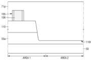
도 19를 참고하면, 제1 소자 영역(AREA 1)과 제2 소자 영역(AREA 2)을 포함하는 제1 기판(100)이 제공된다. 제1 기판(100)은 순차적으로 적층된 베이스 기판(50)과, 프리(pre) 매립 절연막(55a)과, 제1 반도체 기판(110p)을 포함할 수 있다.Referring to FIG. 19 , a
제1 소자 영역(AREA 1)의 제1 기판(100) 상에, 제1 게이트 전극(106)을 포함하는 제1 소자 패턴(105)이 형성된다. 제1 소자 패턴(105)은 제1 반도체 기판(110p) 상에 형성된다.A
도 20을 참고하면, 제2 소자 영역(AREA 2)의 제1 반도체 기판(110p)을 식각하여, 프리 매립 절연막(55a)을 노출시키는 제1 기판 트렌치(110t)가 형성될 수 있다. 제1 기판 트렌치(110t)가 형성됨으로써, 제1 반도체 기판 패턴(110)이 형성될 수 있다. 프리 매립 절연막(55a)의 일부가 제거되어, 제1 기판 트렌치(110t)가 형성되는 것으로 도시하였지만, 이에 제한되는 것은 아니다.Referring to FIG. 20 , the
도 21을 참고하면, 제1 기판(100) 상에, 제1 소자 패턴(105)을 덮는 제1 프리 하부 층간 절연막(71p)이 형성될 수 있다. 제1 프리 하부 층간 절연막(71p)은 제1 기판 트렌치(110t)를 채울 수 있다.Referring to FIG. 21 , a first free lower
도 22를 참고하면, 제2 소자 영역(AREA 2)의 제1 프리 하부 층간 절연막(71p)을 식각하여, 제2 소자 영역(AREA 2)의 프리 매립 절연막(55a)을 노출시킬 수 있다.Referring to FIG. 22 , the first free lower
제2 소자 영역(AREA 2)의 제1 프리 하부 층간 절연막(71p)이 식각되어, 제1 소자 영역(AREA 1) 상에 제1 하부 층간 절연막의 제1 부분(71a)가 형성될 수 있다. 이를 통해, 제1 소자 기판 구조체(105st)가 형성될 수 있다. 제2 소자 영역(AREA 2)의 제1 프리 하부 층간 절연막(71p)이 제거되는 영역의 크기에 따라, 제1 소자 기판 구조체(105st)의 측벽의 프로파일이 변할 수 있다.The first free lower
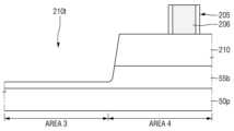
도 23을 참고하면, 제3 소자 영역(AREA 3)과 제4 소자 영역(AREA 4)을 포함하는 제2 기판(200)이 제공된다. 제2 기판(200)은 순차적으로 적층된 더미 베이스 기판(50p)과, 더미 매립 절연막(55b)과, 제2 반도체 기판(210p)을 포함할 수 있다.Referring to FIG. 23 , a
제3 소자 영역(AREA 3)은 제1 기판(100)의 제1 소자 영역(AREA 1)에 대응되고, 제4 소자 영역(AREA 4)은 제1 기판(100)의 제2 소자 영역(AREA 2)에 대응될 수 있다.The third
제4 소자 영역(AREA 4)의 제2 기판(200) 상에, 제2 게이트 전극(206)을 포함하는 제2 소자 패턴(205)이 형성된다. 제2 소자 패턴(205)은 제2 반도체 기판(210p) 상에 형성된다.A
도 24를 참고하면, 제3 소자 영역(AREA 3)의 제2 기판(200)의 일부를 식각하여, 더미 매립 절연막(55b)을 노출시키는 제2 기판 트렌치(210t)가 형성될 수 있다. 예를 들어, 제3 소자 영역(AREA 3)의 제2 반도체 기판(210p)을 식각하여, 더미 매립 절연막(55b)을 노출시키는 제2 기판 트렌치(210t)가 형성될 수 있다.Referring to FIG. 24 , a
제2 기판 트렌치(210t)가 형성됨으로써, 제2 반도체 기판 패턴(210)이 형성될 수 있다. 더미 매립 절연막(55b)의 일부가 제거되어, 제2 기판 트렌치(210t)가 형성되는 것으로 도시하였지만, 이에 제한되는 것은 아니다.By forming the
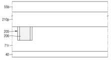
도 25를 참고하면, 제2 기판(200) 상에, 제2 소자 패턴(205)을 덮는 제2 프리 하부 층간 절연막(71r)이 형성될 수 있다. 제2 프리 하부 층간 절연막(71r)은 제2 기판 트렌치(210t)를 채울 수 있다.Referring to FIG. 25 , a second free lower
도 26을 참고하면, 제2 프리 하부 층간 절연막(71r)을 기판 서포터(40)에 본딩시킬 수 있다.Referring to FIG. 26 , the second free lower
이어서, 더미 베이스 기판(50p)을 제거하여, 더미 매립 절연막(55b)이 노출될 수 있다. 이 때, 더미 매립 절연막(55b)의 일부를 제거하여, 더미 매립 절연막(55b)의 두께가 조절될 수 있지만, 이에 제한되는 것은 아니다.Subsequently, the dummy filling insulating
도 27을 참고하면, 제3 소자 영역(도 25의 AREA 3)의 제2 기판(200) 및 제2 프리 하부 층간 절연막(71r)의 적어도 일부가 제거될 수 있다. 즉, 제3 소자 영역(AREA 3)의 더미 매립 절연막(55b)과, 제2 프리 하부 층간 절연막(71r)의 적어도 일부가 제거되어, 제4 소자 영역(AREA 4) 상에 제1 하부 층간 절연막의 제2 부분(71b)이 형성될 수 있다. 이를 통해, 기판 서포터(40) 상에 제2 소자 기판 구조체(205st)가 형성될 수 있다.Referring to FIG. 27 , at least a portion of the
도 28을 참고하면, 제2 소자 기판 구조체(205st)를 제1 소자 기판 구조체(105st)에 본딩하여, 소자 접합 기판(100st)이 형성될 수 있다.Referring to FIG. 28 , the device bonding substrate 100st may be formed by bonding the second device substrate structure 205st to the first device substrate structure 105st.
제2 소자 기판 구조체(205st)의 더미 매립 절연막(55b)을 노출된 제2 소자 영역(AREA 2)의 프리 매립 절연막(55a)에 본딩함으로써, 소자 접합 기판(100st)이 형성될 수 있다.The device bonding substrate 100st may be formed by bonding the dummy filling insulating
이를 통해, 제1 소자 영역(AREA 1)에, 제1 반도체 기판 패턴(110) 및 제1 소자 패턴(105)이 위치하고, 제2 소자 영역(AREA 2)에 제2 반도체 기판 패턴(210) 및 제2 소자 패턴(205)이 위치할 수 있다.Through this, the first
또한, 제2 소자 기판 구조체(205st)를 제1 소자 기판 구조체(105st)에 본딩됨으로써, 제1 반도체 기판 패턴(110) 및 제2 반도체 기판 패턴(210) 사이에 분리 트렌치(60)가 형성될 수 있다.In addition, an
도 29를 참고하면, 기판 서포터(40)는 제거될 수 있다. 또한, 본딩된 더미 매립 절연막(55b) 및 프리 매립 절연막(55a)은 매립 절연막(55)이 될 수 있다.Referring to FIG. 29 , the
이어서, 제1 하부 층간 절연막의 제1 부분(71a) 및 제1 하부 층간 절연막의 제2 부분(71b) 사이에, 필링 층간 절연막(71c)이 형성될 수 있다. 필링 층간 절연막(71c)는 분리 트렌치(60)를 채울 수 있다. 필링 층간 절연막(71c)은 갭필(gap-fill) 능력이 우수한 절연 물질을 포함할 수 있다.Subsequently, a filling
이를 통해, 제1 하부 층간 절연막의 제1 부분(71a), 제1 하부 층간 절연막의 제2 부분(71b) 및 필링 층간 절연막(71c)을 포함하는 제1 하부 층간 절연막(71)이 형성될 수 있다.Through this, the first lower
도 2에서, 제1 하부 층간 절연막(71) 상에, 제1 소자 패턴(105) 및 제2 소자 패턴(205)을 전기적으로 연결하는 제1 통합 연결 배선(75)이 형성될 수 있다.2 , a first
도 30은 본 발명의 몇몇 실시예들에 따른 반도체 장치 제조 방법을 설명하기 위한 중간단계 도면이다.30 is an intermediate step diagram for explaining a method of manufacturing a semiconductor device according to some embodiments of the inventive concept.
도 30을 참고하면, 제1 반도체 기판(110p) 상에, 제1 소자 패턴(105)을 덮는 제1 프리 하부 층간 절연막(71p)이 형성될 수 있다.Referring to FIG. 30 , a first free lower
이어서, 도 22에서, 제2 소자 영역(AREA 2)의 제1 프리 하부 층간 절연막(71p) 및 제1 반도체 기판(110p)을 식각하여, 프리 매립 절연막(55a)을 노출시킬 수 있다. 이를 통해, 제1 소자 기판 구조체(105st)가 형성될 수 있다.22 , the first free lower
도 31 및 도 32는 본 발명의 몇몇 실시예들에 따른 반도체 장치 제조 방법을 설명하기 위한 중간단계 도면들이다.31 and 32 are intermediate diagrams for explaining a method of manufacturing a semiconductor device according to some embodiments of the present invention.
도 31을 참고하면, 제2 반도체 기판(210p) 상에, 제2 소자 패턴(205)을 덮는 제2 프리 하부 층간 절연막(71r)이 형성될 수 있다.Referring to FIG. 31 , a second free lower
도 32를 참고하면, 제2 프리 하부 층간 절연막(71r)을 기판 서포터(40)에 본딩시킬 수 있다. 더미 베이스 기판(50p)을 제거하여, 더미 매립 절연막(55b)이 노출될 수 있다.Referring to FIG. 32 , the second free lower
이어서, 제3 소자 영역(도 25의 AREA 3)의 더미 매립 절연막(55b)과, 제2 반도체 기판과, 제2 프리 하부 층간 절연막(71r)의 적어도 일부가 제거될 수 있다. 이를 통해, 기판 서포터(40) 상에 제2 소자 기판 구조체(205st)가 형성될 수 있다.Subsequently, at least a portion of the dummy buried insulating
도 33 내지 도 36은 본 발명의 몇몇 실시예들에 따른 반도체 장치 제조 방법을 설명하기 위한 도면이다. 도 33 내지 도 36을 이용하여 설명하는 실시예는 제2 기판(200)이 SOI 기판이 아닌 실리콘 기판일 수 있다.33 to 36 are diagrams for explaining a method of manufacturing a semiconductor device according to some example embodiments. In the embodiment described with reference to FIGS. 33 to 36 , the
도 33을 참고하면, 제2 소자 패턴(205)이 형성되지 않은 제3 소자 영역(AREA 3)의 제2 기판(200)의 적어도 일부를 제거하여, 제2 기판 트렌치(210t)가 형성될 수 있다. 제2 기판(200) 상에, 제2 소자 패턴(205)을 덮고 제2 기판 트렌치(210t)를 채우는 제2 프리 하부 층간 절연막(71r)이 형성될 수 있다.Referring to FIG. 33 , a
도 34를 참고하면, 제2 프리 하부 층간 절연막(71r)을 기판 서포터(40)에 본딩시킬 수 있다. 기판 서포터(40)에 본딩된 제2 기판(200)의 일부를 제거하여, 제2 기판(200)의 두께를 감소시킬 수 있다.Referring to FIG. 34 , the second free lower
도 35를 참고하면, 두께가 감소된 제2 기판(200) 상에, 접합 절연막(55c)가 형성될 수 있다. 접합 절연막(55c)은 실리콘 산화물을 포함할 수 있다.Referring to FIG. 35 , a
도 36을 참고하면, 제3 소자 영역(AREA 3)의 접합 절연막(55c)과, 제2 프리 하부 층간 절연막(71r)의 적어도 일부가 제거되어, 제4 소자 영역(AREA 4) 상에 제1 하부 층간 절연막의 제2 부분(71b)이 형성될 수 있다. 이를 통해, 기판 서포터(40) 상에 제2 소자 기판 구조체(205st)가 형성될 수 있다.Referring to FIG. 36 , the
이상 첨부된 도면을 참조하여 본 발명의 실시예를 설명하였지만, 본 발명이 속하는 기술분야에서 통상의 지식을 가진 자는 본 발명이 그 기술적 사상이나 필수적인 특징을 변경하지 않고서 다른 구체적인 형태로 실시될 수 있다는 것을 이해할 수 있을 것이다. 그러므로 이상에서 기술한 실시예들은 모든 면에서 예시적인 것이며 한정적이 아닌 것으로 이해해야만 한다.Although the embodiments of the present invention have been described with reference to the accompanying drawings, those skilled in the art can realize that the present invention can be implemented in other specific forms without changing the technical spirit or essential features. you will be able to understand Therefore, the embodiments described above should be understood as illustrative in all respects and not limiting.
50: 베이스 기판55: 매립 절연막
60: 분리 트렌치70, 80, 90: 층간 절연막
75, 85: 통합 연결 배선105, 205: 소자 패턴
110, 210: 반도체 기판 패턴120, 220: 식각 정지막50: base substrate 55: buried insulating film
60:
75, 85: integrated
110, 210:
Claims (20)
Translated fromKorean상기 베이스 기판 상의 매립 절연막;
상기 매립 절연막 상의 제1 반도체 기판 패턴;
상기 매립 절연막 상에, 상기 제1 반도체 기판 패턴과 이격되는 제2 반도체 기판 패턴;
상기 제1 반도체 기판 패턴 상의 제1 게이트 전극을 포함하는 제1 소자 패턴;
상기 제2 반도체 기판 패턴 상의 제2 게이트 전극을 포함하는 제2 소자 패턴;
상기 제1 반도체 기판 패턴 및 상기 제2 반도체 기판 패턴 사이와, 상기 매립 절연막 내에 형성되고, 서로 마주보는 제1 측벽 및 제2 측벽을 포함하는 분리 트렌치; 및
상기 제1 소자 패턴 및 상기 제2 소자 패턴을 덮고, 상기 분리 트렌치를 완전히 채우는 하부 층간 절연막을 포함하고,
상기 분리 트렌치의 제1 측벽은 상기 제1 반도체 기판 패턴 및 상기 매립 절연막에 의해 정의되고, 상기 분리 트렌치의 제2 측벽은 상기 제2 반도체 기판 패턴 및 상기 매립 절연막에 의해 정의되고,
상기 제1 반도체 기판 패턴에 의해 정의되는 상기 분리 트렌치의 제1 측벽과, 상기 매립 절연막에 의해 정의되는 상기 분리 트렌치의 제1 측벽은 연속되고,
상기 제2 반도체 기판 패턴에 의해 정의되는 상기 분리 트렌치의 제2 측벽과, 상기 매립 절연막에 의해 정의되는 상기 분리 트렌치의 제2 측벽은 연속되는 반도체 장치.base substrate;
a buried insulating film on the base substrate;
a first semiconductor substrate pattern on the filling insulating layer;
a second semiconductor substrate pattern spaced apart from the first semiconductor substrate pattern on the filling insulating layer;
a first element pattern including a first gate electrode on the first semiconductor substrate pattern;
a second element pattern including a second gate electrode on the second semiconductor substrate pattern;
a separation trench formed between the first semiconductor substrate pattern and the second semiconductor substrate pattern and within the buried insulating layer, and including first sidewalls and second sidewalls facing each other; and
a lower interlayer insulating layer covering the first device pattern and the second device pattern and completely filling the isolation trench;
A first sidewall of the isolation trench is defined by the first semiconductor substrate pattern and the insulating filling layer, and a second sidewall of the isolation trench is defined by the second semiconductor substrate pattern and the insulating filling layer;
A first sidewall of the isolation trench defined by the first semiconductor substrate pattern and a first sidewall of the isolation trench defined by the filling insulating layer are continuous;
The semiconductor device of claim 1 , wherein a second sidewall of the isolation trench defined by the second semiconductor substrate pattern and a second sidewall of the isolation trench defined by the filling insulating layer are continuous.
상기 제1 반도체 기판 패턴 및 상기 제2 반도체 기판 패턴은 각각 상기 매립 절연막과 마주보는 하면을 포함하고,
상기 제1 반도체 기판 패턴의 하면과 상기 제1 반도체 기판 패턴에 의해 정의되는 상기 분리 트렌치의 제1 측벽은 예각을 이루고,
상기 제2 반도체 기판 패턴의 하면과 상기 제2 반도체 기판 패턴에 의해 정의되는 상기 분리 트렌치의 제2 측벽의 적어도 일부는 예각을 이루는 반도체 장치.According to claim 1,
The first semiconductor substrate pattern and the second semiconductor substrate pattern each include a lower surface facing the filling insulating layer,
A lower surface of the first semiconductor substrate pattern and a first sidewall of the isolation trench defined by the first semiconductor substrate pattern form an acute angle;
The semiconductor device of claim 1 , wherein a lower surface of the second semiconductor substrate pattern and at least a portion of a second sidewall of the isolation trench defined by the second semiconductor substrate pattern form an acute angle.
상기 제1 반도체 기판 패턴 및 상기 제2 반도체 기판 패턴은 각각 상기 매립 절연막과 마주보는 하면을 포함하고,
상기 제1 반도체 기판 패턴의 하면과 상기 제1 반도체 기판 패턴에 의해 정의되는 상기 분리 트렌치의 제1 측벽은 예각을 이루고,
상기 제2 반도체 기판 패턴의 하면과 상기 제2 반도체 기판 패턴에 의해 정의되는 상기 분리 트렌치의 제2 측벽은 둔각을 이루는 반도체 장치.According to claim 1,
The first semiconductor substrate pattern and the second semiconductor substrate pattern each include a lower surface facing the filling insulating layer,
A lower surface of the first semiconductor substrate pattern and a first sidewall of the isolation trench defined by the first semiconductor substrate pattern form an acute angle;
The semiconductor device of claim 1 , wherein a lower surface of the second semiconductor substrate pattern and a second sidewall of the isolation trench defined by the second semiconductor substrate pattern form an obtuse angle.
상기 분리 트렌치의 제1 측벽과 상기 분리 트렌치의 바닥면은 둔각을 이루고,
상기 분리 트렌치의 제2 측벽은 상기 분리 트렌치의 바닥면에 대해 둔각을 이루는 부분과, 예각을 이루는 부분을 포함하는 반도체 장치.According to claim 1,
A first sidewall of the isolation trench and a bottom surface of the isolation trench form an obtuse angle;
The semiconductor device of claim 1 , wherein the second sidewall of the isolation trench includes a portion forming an obtuse angle and a portion forming an acute angle with respect to a bottom surface of the isolation trench.
상기 제1 반도체 기판 패턴 상에 제1 소자 패턴의 적어도 일부를 따라 연장되는 제1 식각 정지막과, 상기 제2 반도체 기판 패턴 상에 제2 소자 패턴의 적어도 일부를 따라 연장되는 제2 식각 정지막을 더 포함하고,
상기 제1 식각 정지막 및 상기 제2 식각 정지막은 서로 이격되고,
상기 하부 층간 절연막은 상기 제1 및 제2 식각 정지막 상에 형성되는 반도체 장치.According to claim 1,
a first etch stop layer extending along at least a portion of the first device pattern on the first semiconductor substrate pattern and a second etch stop layer extending along at least a portion of the second device pattern on the second semiconductor substrate pattern; contain more,
The first etch stop layer and the second etch stop layer are spaced apart from each other,
The lower interlayer insulating layer is formed on the first and second etch stop layers.
상기 하부 층간 절연막 상에, 상부 층간 절연막과 상기 상부 층간 절연막 내의 통합(integration) 연결 배선을 더 포함하고,
상기 통합 연결 배선의 일부는 상기 분리 트렌치를 가로질러 형성되는 반도체 장치.According to claim 1,
On the lower interlayer insulating film, further comprising an upper interlayer insulating film and an integration connection wiring in the upper interlayer insulating film,
A portion of the integrated connection line is formed across the isolation trench.
상기 제1 반도체 기판 패턴과 중첩되는 영역의 상기 하부 층간 절연막 내에 형성되는 제1 연결 배선과,
상기 제2 반도체 기판 패턴과 중첩되는 영역의 상기 하부 층간 절연막 내에 형성되는 제2 연결 배선을 더 포함하고,
상기 통합 연결 배선은 상기 제1 연결 배선과 상기 제2 연결 배선을 전기적으로 연결하는 반도체 장치.According to claim 6,
a first connection wire formed in the lower interlayer insulating film in a region overlapping the first semiconductor substrate pattern;
Further comprising a second connection wire formed in the lower interlayer insulating film in a region overlapping the second semiconductor substrate pattern,
The integrated connection wire electrically connects the first connection wire and the second connection wire.
상기 제1 소자 패턴은 제1 트랜지스터를 포함하고, 상기 제2 소자 패턴은 제2 트랜지스터를 포함하고,
상기 제1 트랜지스터의 채널 영역의 모양은 상기 제2 트랜지스터의 채널 영역의 모양과 다른 반도체 장치.According to claim 1,
The first device pattern includes a first transistor, the second device pattern includes a second transistor,
A shape of a channel region of the first transistor is different from a shape of a channel region of the second transistor.
상기 제1 소자 패턴은 제1 트랜지스터를 포함하고, 상기 제2 소자 패턴은 제2 트랜지스터를 포함하고,
상기 제1 트랜지스터의 채널 영역의 물질은 상기 제2 트랜지스터의 채널 영역의 물질과 다른 반도체 장치.According to claim 1,
The first device pattern includes a first transistor, the second device pattern includes a second transistor,
A material of a channel region of the first transistor is different from a material of a channel region of the second transistor.
상기 베이스 기판 상의 매립 절연막;
상기 매립 절연막 상의 제1 반도체 기판 패턴;
상기 매립 절연막 상에, 상기 제1 반도체 기판 패턴과 이격되는 제2 반도체 기판 패턴;
상기 제1 반도체 기판 패턴 상의 제1 소자 패턴;
상기 제2 반도체 기판 패턴 상의 제2 소자 패턴;
상기 제1 반도체 기판 패턴 및 상기 제2 반도체 기판 패턴 사이와, 상기 매립 절연막 내에 형성되고, 서로 마주보는 제1 측벽 및 제2 측벽을 포함하는 분리 트렌치; 및
상기 제1 소자 패턴 및 상기 제2 소자 패턴을 덮고, 상기 분리 트렌치를 완전히 채우는 하부 층간 절연막을 포함하고,
상기 분리 트렌치의 제1 측벽과 상기 분리 트렌치의 바닥면의 연결 부분은 라운딩되어 있고,
상기 분리 트렌치의 제2 측벽과 상기 분리 트렌치의 바닥면의 연결 부분은 라운딩되지 않은 반도체 장치.base substrate;
a buried insulating film on the base substrate;
a first semiconductor substrate pattern on the filling insulating layer;
a second semiconductor substrate pattern spaced apart from the first semiconductor substrate pattern on the filling insulating layer;
a first element pattern on the first semiconductor substrate pattern;
a second element pattern on the second semiconductor substrate pattern;
a separation trench formed between the first semiconductor substrate pattern and the second semiconductor substrate pattern and within the buried insulating layer, and including first sidewalls and second sidewalls facing each other; and
a lower interlayer insulating layer covering the first device pattern and the second device pattern and completely filling the isolation trench;
A connection portion between a first sidewall of the isolation trench and a bottom surface of the isolation trench is rounded;
A connection portion between the second sidewall of the isolation trench and the bottom surface of the isolation trench is not rounded.
상기 분리 트렌치의 제1 측벽은 상기 제1 반도체 기판 패턴 및 상기 매립 절연막에 의해 정의되고, 상기 분리 트렌치의 제2 측벽은 상기 제2 반도체 기판 패턴 및 상기 매립 절연막에 의해 정의되고,
상기 제1 반도체 기판 패턴에 의해 정의되는 상기 분리 트렌치의 제1 측벽과, 상기 매립 절연막에 의해 정의되는 상기 분리 트렌치의 제1 측벽은 연속되고,
상기 제2 반도체 기판 패턴에 의해 정의되는 상기 분리 트렌치의 제2 측벽과, 상기 매립 절연막에 의해 정의되는 상기 분리 트렌치의 제2 측벽은 연속되는 반도체 장치.According to claim 10,
A first sidewall of the isolation trench is defined by the first semiconductor substrate pattern and the insulating filling layer, and a second sidewall of the isolation trench is defined by the second semiconductor substrate pattern and the insulating filling layer;
A first sidewall of the isolation trench defined by the first semiconductor substrate pattern and a first sidewall of the isolation trench defined by the filling insulating layer are continuous;
The semiconductor device of claim 1 , wherein a second sidewall of the isolation trench defined by the second semiconductor substrate pattern and a second sidewall of the isolation trench defined by the filling insulating layer are continuous.
상기 제1 반도체 기판 패턴 및 상기 제2 반도체 기판 패턴은 각각 상기 매립 절연막과 마주보는 하면을 포함하고,
상기 제1 반도체 기판 패턴의 하면과 상기 제1 반도체 기판 패턴에 의해 정의되는 상기 분리 트렌치의 제1 측벽은 예각을 이루고,
상기 제2 반도체 기판 패턴의 하면과 상기 제2 반도체 기판 패턴에 의해 정의되는 상기 분리 트렌치의 제2 측벽의 적어도 일부는 예각을 이루는 반도체 장치.According to claim 10,
The first semiconductor substrate pattern and the second semiconductor substrate pattern each include a lower surface facing the filling insulating layer,
A lower surface of the first semiconductor substrate pattern and a first sidewall of the isolation trench defined by the first semiconductor substrate pattern form an acute angle;
The semiconductor device of claim 1 , wherein a lower surface of the second semiconductor substrate pattern and at least a portion of a second sidewall of the isolation trench defined by the second semiconductor substrate pattern form an acute angle.
상기 제1 반도체 기판 패턴 및 상기 제2 반도체 기판 패턴은 각각 상기 매립 절연막과 마주보는 하면을 포함하고,
상기 제1 반도체 기판 패턴의 하면과 상기 제1 반도체 기판 패턴에 의해 정의되는 상기 분리 트렌치의 제1 측벽은 예각을 이루고,
상기 제2 반도체 기판 패턴의 하면과 상기 제2 반도체 기판 패턴에 의해 정의되는 상기 분리 트렌치의 제2 측벽은 둔각을 이루는 반도체 장치.According to claim 10,
The first semiconductor substrate pattern and the second semiconductor substrate pattern each include a lower surface facing the filling insulating layer,
A lower surface of the first semiconductor substrate pattern and a first sidewall of the isolation trench defined by the first semiconductor substrate pattern form an acute angle;
The semiconductor device of claim 1 , wherein a lower surface of the second semiconductor substrate pattern and a second sidewall of the isolation trench defined by the second semiconductor substrate pattern form an obtuse angle.
상기 분리 트렌치의 제1 측벽과 상기 분리 트렌치의 바닥면은 둔각을 이루고,
상기 분리 트렌치의 제2 측벽은 상기 분리 트렌치의 바닥면에 대해 둔각을 이루는 부분과, 예각을 이루는 부분을 포함하는 반도체 장치.According to claim 10,
A first sidewall of the isolation trench and a bottom surface of the isolation trench form an obtuse angle;
The semiconductor device of claim 1 , wherein the second sidewall of the isolation trench includes a portion forming an obtuse angle and a portion forming an acute angle with respect to a bottom surface of the isolation trench.
상기 베이스 기판 상의 매립 절연막;
상기 매립 절연막 상의 제1 반도체 기판 패턴;
상기 매립 절연막 상에, 상기 제1 반도체 기판 패턴과 이격되는 제2 반도체 기판 패턴;
상기 제1 반도체 기판 패턴 상의 제1 소자 패턴;
상기 제2 반도체 기판 패턴 상의 제2 소자 패턴;
상기 제1 반도체 기판 패턴 및 상기 제2 반도체 기판 패턴 사이와, 상기 매립 절연막 내에 형성되고, 서로 마주보는 제1 측벽 및 제2 측벽을 포함하는 분리 트렌치;
상기 제1 소자 패턴 및 상기 제2 소자 패턴을 덮고, 상기 분리 트렌치를 완전히 채우는 층간 절연막;
상기 층간 절연막 상에, 서로 마주보는 제1 면과 제2 면을 포함하는 제3 반도체 기판 패턴; 및
상기 제3 반도체 기판 패턴의 제1 면 상의 제3 소자 패턴을 포함하는 반도체 장치.base substrate;
a buried insulating film on the base substrate;
a first semiconductor substrate pattern on the filling insulating layer;
a second semiconductor substrate pattern spaced apart from the first semiconductor substrate pattern on the filling insulating layer;
a first element pattern on the first semiconductor substrate pattern;
a second element pattern on the second semiconductor substrate pattern;
a separation trench formed between the first semiconductor substrate pattern and the second semiconductor substrate pattern and within the buried insulating layer, and including first sidewalls and second sidewalls facing each other;
an interlayer insulating layer covering the first device pattern and the second device pattern and completely filling the isolation trench;
a third semiconductor substrate pattern including a first surface and a second surface facing each other on the interlayer insulating film; and
A semiconductor device including a third element pattern on the first surface of the third semiconductor substrate pattern.
상기 제3 반도체 기판 패턴의 제2 면은 상기 층간 절연막과 마주보는 반도체 장치.According to claim 15,
The second surface of the third semiconductor substrate pattern faces the interlayer insulating film.
상기 제3 반도체 기판 패턴과 상기 층간 절연막 사이에, 삽입 매립 절연막과,
상기 삽입 매립 절연막을 관통하는 관통 전극을 더 포함하는 반도체 장치.According to claim 16,
a buried insulating film between the third semiconductor substrate pattern and the interlayer insulating film;
The semiconductor device further includes a penetration electrode penetrating the interstitial insulating layer.
상기 제3 반도체 기판 패턴의 제1 면은 상기 층간 절연막과 마주보는 반도체 장치.According to claim 15,
The semiconductor device of claim 1 , wherein a first surface of the third semiconductor substrate pattern faces the interlayer insulating film.
상기 층간 절연막은 하부 층간 절연막 및 상부 층간 절연막을 포함하고,
상기 하부 층간 절연막 내에 상기 제1 소자 패턴 및 상기 제2 소자 패턴과 전기적으로 연결되는 제1 배선 구조와,
상기 상부 층간 절연막 내에 상기 제3 소자 패턴과 전기적으로 연결되는 제2 배선 구조를 더 포함하고,
상기 제1 배선 구조는 상기 제2 배선 구조와 연결되는 반도체 장치.According to claim 18,
The interlayer insulating film includes a lower interlayer insulating film and an upper interlayer insulating film,
a first wiring structure electrically connected to the first element pattern and the second element pattern within the lower interlayer insulating film;
A second wiring structure electrically connected to the third element pattern in the upper interlayer insulating film;
The first wiring structure is connected to the second wiring structure.
상기 제1 소자 영역에 대응되는 제3 소자 영역과, 상기 제2 소자 영역에 대응되는 제4 소자 영역을 포함하는 제2 기판을 제공하고,
상기 제1 소자 영역의 상기 제1 반도체 기판 상에, 제1 소자 패턴을 형성하고,
상기 제2 소자 영역의 상기 제1 반도체 기판을 식각하여, 상기 제1 매립 절연막을 노출시키는 제1 트렌치를 형성하고,
상기 제1 기판 상에, 상기 제1 소자 패턴을 덮고, 상기 제1 트렌치를 채우는 제1 층간 절연막을 형성하고,
상기 제2 소자 영역의 상기 제1 층간 절연막을 식각하여, 상기 제2 소자 영역의 상기 제1 매립 절연막을 노출시키는 제1 소자 기판 구조체를 형성하고,
상기 제4 소자 영역의 상기 제2 기판 상에, 제2 소자 패턴을 형성하고,
상기 제3 소자 영역의 상기 제2 기판의 일부를 제거하여, 제2 트렌치를 형성하고,
상기 제2 기판 상에, 상기 제2 소자 패턴을 덮고, 상기 제2 트렌치를 채우는 제2 층간 절연막을 형성하고,
상기 제2 층간 절연막을 기판 서포터에 본딩한 후, 상기 제3 소자 영역의 상기 제2 기판 및 상기 제2 층간 절연막의 적어도 일부를 제거하여, 상기 기판 서포터 상에 제2 소자 기판 구조체를 형성하고,
상기 제2 소자 영역과 상기 제3 소자 영역이 대응하도록 상기 제1 소자 기판 구조체 및 상기 제2 소자 기판 구조체를 본딩하여, 소자 접합 기판을 형성하는 것을 포함하는 반도체 장치 제조 방법.providing a first substrate including a first device region and a second device region, and on which a first base substrate, a first buried insulating film, and a first semiconductor substrate are sequentially stacked;
providing a second substrate including a third device region corresponding to the first device region and a fourth device region corresponding to the second device region;
forming a first device pattern on the first semiconductor substrate in the first device region;
etching the first semiconductor substrate in the second device region to form a first trench exposing the first buried insulating layer;
forming a first interlayer insulating film on the first substrate, covering the first element pattern and filling the first trench;
etching the first insulating interlayer in the second device region to form a first device substrate structure exposing the first buried insulating layer in the second device region;
forming a second element pattern on the second substrate in the fourth element region;
forming a second trench by removing a portion of the second substrate in the third device region;
forming a second interlayer insulating film on the second substrate, covering the second element pattern and filling the second trench;
After bonding the second interlayer insulating film to the substrate supporter, forming a second element substrate structure on the substrate supporter by removing at least a portion of the second substrate and the second interlayer insulating film in the third element region;
and forming an element bonded substrate by bonding the first element substrate structure and the second element substrate structure so that the second element region and the third element region correspond to each other.
Priority Applications (4)
| Application Number | Priority Date | Filing Date | Title |
|---|---|---|---|
| KR1020160171662AKR102530338B1 (en) | 2016-12-15 | 2016-12-15 | Semiconductor device and method for fabricating the same |
| TW106125037ATWI729177B (en) | 2016-12-15 | 2017-07-26 | Semiconductor device |
| CN201711107813.0ACN108231890B (en) | 2016-12-15 | 2017-11-10 | Semiconductor device |
| US15/843,139US10453864B2 (en) | 2016-12-15 | 2017-12-15 | Semiconductor device and method for fabricating the same |
Applications Claiming Priority (1)
| Application Number | Priority Date | Filing Date | Title |
|---|---|---|---|
| KR1020160171662AKR102530338B1 (en) | 2016-12-15 | 2016-12-15 | Semiconductor device and method for fabricating the same |
Publications (2)
| Publication Number | Publication Date |
|---|---|
| KR20180069459A KR20180069459A (en) | 2018-06-25 |
| KR102530338B1true KR102530338B1 (en) | 2023-05-08 |
Family
ID=62562714
Family Applications (1)
| Application Number | Title | Priority Date | Filing Date |
|---|---|---|---|
| KR1020160171662AActiveKR102530338B1 (en) | 2016-12-15 | 2016-12-15 | Semiconductor device and method for fabricating the same |
Country Status (4)
| Country | Link |
|---|---|
| US (1) | US10453864B2 (en) |
| KR (1) | KR102530338B1 (en) |
| CN (1) | CN108231890B (en) |
| TW (1) | TWI729177B (en) |
Families Citing this family (3)
| Publication number | Priority date | Publication date | Assignee | Title |
|---|---|---|---|---|
| US11121224B2 (en)* | 2019-02-08 | 2021-09-14 | Texas Instruments Incorporated | Transistor with field plate over tapered trench isolation |
| KR102714154B1 (en)* | 2019-03-25 | 2024-10-07 | 삼성전자주식회사 | Method for fabricating semiconductor device |
| CN117476549B (en)* | 2023-12-25 | 2024-04-09 | 合肥晶合集成电路股份有限公司 | Method for manufacturing semiconductor laminated structure and semiconductor structure |
Citations (4)
| Publication number | Priority date | Publication date | Assignee | Title |
|---|---|---|---|---|
| US20070057302A1 (en)* | 2005-09-09 | 2007-03-15 | International Business Machines Corporation | Trench metal-insulator-metal (mim) capacitors integrated with middle-of-line metal contacts, and method of fabricating same |
| US20070164443A1 (en)* | 2005-09-29 | 2007-07-19 | Atmel Germany Gmbh | Semiconductor array and method for manufacturing a semiconductor array |
| US20140091281A1 (en)* | 2012-10-02 | 2014-04-03 | International Business Machines Corporation | Non-volatile memory device employing semiconductor nanoparticles |
| US20170084531A1 (en) | 2015-09-22 | 2017-03-23 | Qualcomm Incorporated | Integrated circuits (ics) on a glass substrate |
Family Cites Families (13)
| Publication number | Priority date | Publication date | Assignee | Title |
|---|---|---|---|---|
| US6303460B1 (en)* | 2000-02-07 | 2001-10-16 | Mitsubishi Denki Kabushiki Kaisha | Semiconductor device and method for manufacturing the same |
| KR20040061967A (en)* | 2002-12-31 | 2004-07-07 | 동부전자 주식회사 | Method for forming isolation layer of semiconductor device |
| US7041576B2 (en)* | 2004-05-28 | 2006-05-09 | Freescale Semiconductor, Inc. | Separately strained N-channel and P-channel transistors |
| US8716805B2 (en) | 2008-06-10 | 2014-05-06 | Toshiba America Research, Inc. | CMOS integrated circuits with bonded layers containing functional electronic devices |
| US8455334B2 (en) | 2009-12-04 | 2013-06-04 | International Business Machines Corporation | Planar and nanowire field effect transistors |
| US9219005B2 (en) | 2011-06-28 | 2015-12-22 | Monolithic 3D Inc. | Semiconductor system and device |
| US8859302B2 (en)* | 2011-02-28 | 2014-10-14 | International Business Machines Corporation | Structure and method for adjusting threshold voltage of the array of transistors |
| US8722472B2 (en) | 2011-12-16 | 2014-05-13 | International Business Machines Corporation | Hybrid CMOS nanowire mesh device and FINFET device |
| US8557632B1 (en) | 2012-04-09 | 2013-10-15 | Monolithic 3D Inc. | Method for fabrication of a semiconductor device and structure |
| US8536029B1 (en) | 2012-06-21 | 2013-09-17 | International Business Machines Corporation | Nanowire FET and finFET |
| US9385058B1 (en) | 2012-12-29 | 2016-07-05 | Monolithic 3D Inc. | Semiconductor device and structure |
| US9202788B2 (en) | 2013-10-02 | 2015-12-01 | Taiwan Semiconductor Manufacturing Company Limited | Multi-layer semiconductor device structure |
| US9755017B1 (en)* | 2016-03-01 | 2017-09-05 | International Business Machines Corporation | Co-integration of silicon and silicon-germanium channels for nanosheet devices |
- 2016
- 2016-12-15KRKR1020160171662Apatent/KR102530338B1/enactiveActive
- 2017
- 2017-07-26TWTW106125037Apatent/TWI729177B/enactive
- 2017-11-10CNCN201711107813.0Apatent/CN108231890B/enactiveActive
- 2017-12-15USUS15/843,139patent/US10453864B2/enactiveActive
Patent Citations (4)
| Publication number | Priority date | Publication date | Assignee | Title |
|---|---|---|---|---|
| US20070057302A1 (en)* | 2005-09-09 | 2007-03-15 | International Business Machines Corporation | Trench metal-insulator-metal (mim) capacitors integrated with middle-of-line metal contacts, and method of fabricating same |
| US20070164443A1 (en)* | 2005-09-29 | 2007-07-19 | Atmel Germany Gmbh | Semiconductor array and method for manufacturing a semiconductor array |
| US20140091281A1 (en)* | 2012-10-02 | 2014-04-03 | International Business Machines Corporation | Non-volatile memory device employing semiconductor nanoparticles |
| US20170084531A1 (en) | 2015-09-22 | 2017-03-23 | Qualcomm Incorporated | Integrated circuits (ics) on a glass substrate |
Also Published As
| Publication number | Publication date |
|---|---|
| TW201834252A (en) | 2018-09-16 |
| TWI729177B (en) | 2021-06-01 |
| CN108231890A (en) | 2018-06-29 |
| US10453864B2 (en) | 2019-10-22 |
| KR20180069459A (en) | 2018-06-25 |
| CN108231890B (en) | 2023-05-12 |
| US20180175070A1 (en) | 2018-06-21 |
Similar Documents
| Publication | Publication Date | Title |
|---|---|---|
| KR102460847B1 (en) | Semiconductor device and method for fabricating the same | |
| KR102427326B1 (en) | Semiconductor device and method for manufacturing the same | |
| KR102500943B1 (en) | Semiconductor device and method of fabricating thereof | |
| KR102343202B1 (en) | Semiconductor device and method for fabricating the same | |
| CN110299321B (en) | Semiconductor device including self-aligned contacts and method of manufacturing the same | |
| KR102360410B1 (en) | Semiconductor device | |
| KR102557549B1 (en) | Semiconductor device and method for fabricating the same | |
| CN107452797A (en) | Semiconductor devices | |
| US10692781B2 (en) | Semiconductor device | |
| US10804403B2 (en) | Method of fabricating semiconductor devices | |
| KR102772447B1 (en) | Semiconductor device | |
| KR102491555B1 (en) | Semiconductor device and method for fabricating the same | |
| KR20190101609A (en) | Semiconductor device and method for fabricating the same | |
| KR102530338B1 (en) | Semiconductor device and method for fabricating the same | |
| KR20200015160A (en) | Semiconductor device and method for fabricating the same | |
| TW202205621A (en) | Semiconductor device | |
| KR20230012669A (en) | Semiconductor device | |
| KR102388352B1 (en) | Semiconductor device and method for fabricating the same | |
| KR20250027950A (en) | Semiconductor device and method for manufacturing the same | |
| KR20240162277A (en) | Semiconductor devices | |
| KR20240118407A (en) | Semiconductor devices | |
| KR20160144287A (en) | Semiconductor device and method for fabricating the same |
Legal Events
| Date | Code | Title | Description |
|---|---|---|---|
| PA0109 | Patent application | Patent event code:PA01091R01D Comment text:Patent Application Patent event date:20161215 | |
| PG1501 | Laying open of application | ||
| A201 | Request for examination | ||
| PA0201 | Request for examination | Patent event code:PA02012R01D Patent event date:20210603 Comment text:Request for Examination of Application Patent event code:PA02011R01I Patent event date:20161215 Comment text:Patent Application | |
| E902 | Notification of reason for refusal | ||
| PE0902 | Notice of grounds for rejection | Comment text:Notification of reason for refusal Patent event date:20220829 Patent event code:PE09021S01D | |
| E701 | Decision to grant or registration of patent right | ||
| PE0701 | Decision of registration | Patent event code:PE07011S01D Comment text:Decision to Grant Registration Patent event date:20230330 | |
| GRNT | Written decision to grant | ||
| PR0701 | Registration of establishment | Comment text:Registration of Establishment Patent event date:20230503 Patent event code:PR07011E01D | |
| PR1002 | Payment of registration fee | Payment date:20230503 End annual number:3 Start annual number:1 | |
| PG1601 | Publication of registration |