KR102528646B1 - Aperture multiplier using a rectangular waveguide - Google Patents
Aperture multiplier using a rectangular waveguideDownload PDFInfo
- Publication number
- KR102528646B1 KR102528646B1KR1020187007797AKR20187007797AKR102528646B1KR 102528646 B1KR102528646 B1KR 102528646B1KR 1020187007797 AKR1020187007797 AKR 1020187007797AKR 20187007797 AKR20187007797 AKR 20187007797AKR 102528646 B1KR102528646 B1KR 102528646B1
- Authority
- KR
- South Korea
- Prior art keywords
- waveguide
- image
- optical
- coupling
- optical waveguide
- Prior art date
- Legal status (The legal status is an assumption and is not a legal conclusion. Google has not performed a legal analysis and makes no representation as to the accuracy of the status listed.)
- Active
Links
Images


Classifications
- G—PHYSICS
- G02—OPTICS
- G02B—OPTICAL ELEMENTS, SYSTEMS OR APPARATUS
- G02B5/00—Optical elements other than lenses
- G02B5/30—Polarising elements
- G—PHYSICS
- G02—OPTICS
- G02B—OPTICAL ELEMENTS, SYSTEMS OR APPARATUS
- G02B27/00—Optical systems or apparatus not provided for by any of the groups G02B1/00 - G02B26/00, G02B30/00
- G02B27/01—Head-up displays
- G02B27/0101—Head-up displays characterised by optical features
- G—PHYSICS
- G02—OPTICS
- G02B—OPTICAL ELEMENTS, SYSTEMS OR APPARATUS
- G02B1/00—Optical elements characterised by the material of which they are made; Optical coatings for optical elements
- G02B1/10—Optical coatings produced by application to, or surface treatment of, optical elements
- G—PHYSICS
- G02—OPTICS
- G02B—OPTICAL ELEMENTS, SYSTEMS OR APPARATUS
- G02B27/00—Optical systems or apparatus not provided for by any of the groups G02B1/00 - G02B26/00, G02B30/00
- G02B27/0081—Optical systems or apparatus not provided for by any of the groups G02B1/00 - G02B26/00, G02B30/00 with means for altering, e.g. enlarging, the entrance or exit pupil
- G—PHYSICS
- G02—OPTICS
- G02B—OPTICAL ELEMENTS, SYSTEMS OR APPARATUS
- G02B27/00—Optical systems or apparatus not provided for by any of the groups G02B1/00 - G02B26/00, G02B30/00
- G02B27/01—Head-up displays
- G02B27/017—Head mounted
- G02B27/0172—Head mounted characterised by optical features
- G—PHYSICS
- G02—OPTICS
- G02B—OPTICAL ELEMENTS, SYSTEMS OR APPARATUS
- G02B27/00—Optical systems or apparatus not provided for by any of the groups G02B1/00 - G02B26/00, G02B30/00
- G02B27/10—Beam splitting or combining systems
- G—PHYSICS
- G02—OPTICS
- G02B—OPTICAL ELEMENTS, SYSTEMS OR APPARATUS
- G02B27/00—Optical systems or apparatus not provided for by any of the groups G02B1/00 - G02B26/00, G02B30/00
- G02B27/10—Beam splitting or combining systems
- G02B27/14—Beam splitting or combining systems operating by reflection only
- G—PHYSICS
- G02—OPTICS
- G02B—OPTICAL ELEMENTS, SYSTEMS OR APPARATUS
- G02B27/00—Optical systems or apparatus not provided for by any of the groups G02B1/00 - G02B26/00, G02B30/00
- G02B27/28—Optical systems or apparatus not provided for by any of the groups G02B1/00 - G02B26/00, G02B30/00 for polarising
- G02B27/283—Optical systems or apparatus not provided for by any of the groups G02B1/00 - G02B26/00, G02B30/00 for polarising used for beam splitting or combining
- G02B27/285—Optical systems or apparatus not provided for by any of the groups G02B1/00 - G02B26/00, G02B30/00 for polarising used for beam splitting or combining comprising arrays of elements, e.g. microprisms
- G—PHYSICS
- G02—OPTICS
- G02B—OPTICAL ELEMENTS, SYSTEMS OR APPARATUS
- G02B27/00—Optical systems or apparatus not provided for by any of the groups G02B1/00 - G02B26/00, G02B30/00
- G02B27/28—Optical systems or apparatus not provided for by any of the groups G02B1/00 - G02B26/00, G02B30/00 for polarising
- G02B27/286—Optical systems or apparatus not provided for by any of the groups G02B1/00 - G02B26/00, G02B30/00 for polarising for controlling or changing the state of polarisation, e.g. transforming one polarisation state into another
- G—PHYSICS
- G02—OPTICS
- G02B—OPTICAL ELEMENTS, SYSTEMS OR APPARATUS
- G02B6/00—Light guides; Structural details of arrangements comprising light guides and other optical elements, e.g. couplings
- G02B6/0001—Light guides; Structural details of arrangements comprising light guides and other optical elements, e.g. couplings specially adapted for lighting devices or systems
- G02B6/0011—Light guides; Structural details of arrangements comprising light guides and other optical elements, e.g. couplings specially adapted for lighting devices or systems the light guides being planar or of plate-like form
- G02B6/0013—Means for improving the coupling-in of light from the light source into the light guide
- G02B6/0023—Means for improving the coupling-in of light from the light source into the light guide provided by one optical element, or plurality thereof, placed between the light guide and the light source, or around the light source
- G02B6/0028—Light guide, e.g. taper
- G—PHYSICS
- G02—OPTICS
- G02B—OPTICAL ELEMENTS, SYSTEMS OR APPARATUS
- G02B6/00—Light guides; Structural details of arrangements comprising light guides and other optical elements, e.g. couplings
- G02B6/0001—Light guides; Structural details of arrangements comprising light guides and other optical elements, e.g. couplings specially adapted for lighting devices or systems
- G02B6/0011—Light guides; Structural details of arrangements comprising light guides and other optical elements, e.g. couplings specially adapted for lighting devices or systems the light guides being planar or of plate-like form
- G02B6/0033—Means for improving the coupling-out of light from the light guide
- G02B6/0035—Means for improving the coupling-out of light from the light guide provided on the surface of the light guide or in the bulk of it
- G02B6/0036—2-D arrangement of prisms, protrusions, indentations or roughened surfaces
- G—PHYSICS
- G02—OPTICS
- G02B—OPTICAL ELEMENTS, SYSTEMS OR APPARATUS
- G02B6/00—Light guides; Structural details of arrangements comprising light guides and other optical elements, e.g. couplings
- G02B6/10—Light guides; Structural details of arrangements comprising light guides and other optical elements, e.g. couplings of the optical waveguide type
- G—PHYSICS
- G02—OPTICS
- G02B—OPTICAL ELEMENTS, SYSTEMS OR APPARATUS
- G02B6/00—Light guides; Structural details of arrangements comprising light guides and other optical elements, e.g. couplings
- G02B6/24—Coupling light guides
- G02B6/26—Optical coupling means
- G—PHYSICS
- G02—OPTICS
- G02B—OPTICAL ELEMENTS, SYSTEMS OR APPARATUS
- G02B6/00—Light guides; Structural details of arrangements comprising light guides and other optical elements, e.g. couplings
- G02B6/24—Coupling light guides
- G02B6/26—Optical coupling means
- G02B6/27—Optical coupling means with polarisation selective and adjusting means
- G02B6/2753—Optical coupling means with polarisation selective and adjusting means characterised by their function or use, i.e. of the complete device
- G02B6/2786—Reducing the polarisation degree, i.e. depolarisers, scramblers, unpolarised output
- G—PHYSICS
- G02—OPTICS
- G02F—OPTICAL DEVICES OR ARRANGEMENTS FOR THE CONTROL OF LIGHT BY MODIFICATION OF THE OPTICAL PROPERTIES OF THE MEDIA OF THE ELEMENTS INVOLVED THEREIN; NON-LINEAR OPTICS; FREQUENCY-CHANGING OF LIGHT; OPTICAL LOGIC ELEMENTS; OPTICAL ANALOGUE/DIGITAL CONVERTERS
- G02F1/00—Devices or arrangements for the control of the intensity, colour, phase, polarisation or direction of light arriving from an independent light source, e.g. switching, gating or modulating; Non-linear optics
- G02F1/29—Devices or arrangements for the control of the intensity, colour, phase, polarisation or direction of light arriving from an independent light source, e.g. switching, gating or modulating; Non-linear optics for the control of the position or the direction of light beams, i.e. deflection
- G02F1/295—Analog deflection from or in an optical waveguide structure]
- H—ELECTRICITY
- H04—ELECTRIC COMMUNICATION TECHNIQUE
- H04N—PICTORIAL COMMUNICATION, e.g. TELEVISION
- H04N5/00—Details of television systems
- H04N5/74—Projection arrangements for image reproduction, e.g. using eidophor
- G—PHYSICS
- G02—OPTICS
- G02B—OPTICAL ELEMENTS, SYSTEMS OR APPARATUS
- G02B27/00—Optical systems or apparatus not provided for by any of the groups G02B1/00 - G02B26/00, G02B30/00
- G02B27/01—Head-up displays
- G02B27/0101—Head-up displays characterised by optical features
- G02B2027/0123—Head-up displays characterised by optical features comprising devices increasing the field of view
- G02B2027/0125—Field-of-view increase by wavefront division
Landscapes
- Physics & Mathematics (AREA)
- Optics & Photonics (AREA)
- General Physics & Mathematics (AREA)
- Nonlinear Science (AREA)
- Signal Processing (AREA)
- Multimedia (AREA)
- Engineering & Computer Science (AREA)
- Optical Couplings Of Light Guides (AREA)
- Optical Elements Other Than Lenses (AREA)
- Complex Calculations (AREA)
- Measuring Pulse, Heart Rate, Blood Pressure Or Blood Flow (AREA)
- Measuring And Recording Apparatus For Diagnosis (AREA)
- Light Guides In General And Applications Therefor (AREA)
- Polarising Elements (AREA)
Abstract
Translated fromKoreanDescription
Translated fromKorean본 발명은 광학 개구 배율기에 관한 것으로, 특히 직사각형 도파관을 포함하는 광학 개구 배율기, 및 이러한 개구 배율기를 이용하는 근안(near-eye) 디스플레이 및 헤드업(head-up) 디스플레이에 관한 것이다.The present invention relates to optical aperture multipliers, and more particularly to optical aperture multipliers comprising rectangular waveguides, and near-eye displays and head-up displays using such aperture multipliers.
근안 디스플레이 또는 헤드업 디스플레이용 광학 장치는 관찰자의 눈이 위치하는 공간(눈-동작-박스(eye-motion-box))을 덮기 위해 큰 개구를 필요로 한다. 소형 디바이스를 구현하기 위해, 큰 개구를 생성하도록 배가되는(multiplied), 작은 개구를 갖는 소형 광학 이미지 발생기에 의해 이미지가 생성된다.Optical devices for near-eye displays or heads-up displays require a large aperture to cover a space where an observer's eyes are located (eye-motion-box). To implement a compact device, the image is created by a compact optical image generator with a small aperture that is multiplied to create a large aperture.
일차원의 개구 배가에 대한 접근법은 이미지가 내부 반사에 의해 전파되는 표면이 평행한 투명 물질 슬래브(slab)를 기반으로 개발되었다. 이미지 파면(wavefront)의 일부는 비스듬하게 각진 부분 반사기를 사용하거나 슬래브의 한 면에서 회절 광학 소자를 사용하여 슬래브 외부에 결합된다. 이러한 슬래브는 여기에서 일차원으로 내부 반사에 의해 이미지 파면을 내부에 포함하는 일차원 도파관으로 불린다. 슬래브의 평면에서(즉, 슬래브 표면의 평면에서), 이미지는 도파관을 가로질러 이미지 품질을 유지하도록 시준되어야 한다.Approaches to one-dimensional aperture doubling have been developed based on slabs of transparent material with parallel surfaces through which images propagate by internal reflection. A portion of the image wavefront is coupled to the outside of the slab using an obliquely angled partial reflector or using a diffractive optical element on one side of the slab. Such a slab is referred to herein as a one-dimensional waveguide containing an image wavefront therein by internal reflection in one dimension. In the plane of the slab (i.e., in the plane of the slab surface), the image must be collimated across the waveguide to maintain image quality.
슬래브-전파 접근법은 개구 배가의 제2 단계에 대해 아주 적합한데, 여기서 슬래브는 관찰자의 눈 맞은편에 배치되고(근안 디스플레이용 유리 렌즈, 또는 더욱 큰 헤드업 디스플레이용 창처럼), 이미지가 눈에 도달하는 최종 출력 표면을 형성한다. 그러나 이 접근법은 이미지 파면의 폭에 비해 슬래브의 폭에 대한 요구사항이 디바이스에 벌크 및 중량을 부가하는, 제1 배가(multiplication) 단계에 대해 최적이 아니다.The slab-propagation approach is well suited for the second stage of aperture doubling, where the slab is placed opposite the observer's eye (like a glass lens for a near-eye display, or a window for a larger heads-up display), and the image is visible to the eye. form the final output surface to be reached. However, this approach is not optimal for the first multiplication step, where the requirement for the width of the slab compared to the width of the image wavefront adds bulk and weight to the device.
본 발명은 직사각형 도파관을 포함하는 광학 개구 배율기이다.The present invention is an optical aperture multiplier comprising a rectangular waveguide.
본 발명의 일 실시예의 교시에 따르면, (a) 신장(elongation) 방향을 갖고, 직사각형 횡단면을 형성하는 제1 및 제2 쌍의 평행면을 갖는 제1 광 도파관으로서, 다수의 부분적으로 반사하는 표면은 제1 광 도파관을 적어도 부분적으로 횡단하고, 부분적으로 반사하는 표면은 신장 방향에 대해 경사진 각도로 존재하는, 제1 광 도파관; 및 (b) 제1 광 도파관에 광학적으로 결합되고, 평판형(slab-type) 도파관을 형성하는 제3 쌍의 평행면을 갖는 제2 광 도파관으로서, 다수의 부분적으로 반사하는 표면은 제2 광 도파관을 적어도 부분적으로 횡단하고, 부분적으로 반사하는 표면은 제3 쌍의 평행면에 대해 경사진 각도로 존재하는, 제2 광 도파관을 포함하는 광학 개구 배율기가 제공되며, 제1 및 제2 광 도파관의 광학 결합 및 부분적으로 반사하는 표면은 제1 및 제2 쌍의 평행면 둘 다에 대해 비스듬한 결합 각도에서 초기 전파 방향으로 이미지가 제1 광 도파관에 커플링-인될 때, 이미지는 제2 광 도파관에 커플링-인되도록 부분적으로 반사하는 표면에서 반사된 이미지의 강도의 비율 및 가시적인 이미지로서 평행면 중 하나로부터 외부로 향하도록 부분적으로 반사하는 표면에서 반사된 이미지의 강도의 비율로 제1 광 도파관을 따라 4-접(4-fold) 내부 반사에 의해 진행한다.According to the teachings of an embodiment of the present invention, (a) a first light guide having a first and second pair of parallel planes having a direction of elongation and defining a rectangular cross-section, wherein the plurality of partially reflective surfaces comprises: a first optical waveguide at least partially transverse to the first optical waveguide, wherein the partially reflective surface is at an oblique angle with respect to the direction of extension; and (b) a second optical waveguide optically coupled to the first optical waveguide and having a third pair of parallel planes forming a slab-type waveguide, the plurality of partially reflective surfaces comprising the second optical waveguide. An optical aperture multiplier comprising a second optical waveguide at least partially transverses and the partially reflective surface is at an oblique angle with respect to a third pair of parallel planes, wherein the optical aperture multiplier of the first and second optical waveguides is provided. The coupling and partially reflective surfaces have an oblique coupling angle with respect to both the first and second pairs of parallel planes, in an initial direction of propagation, when an image is coupled-in to the first optical waveguide, the image is coupled to the second optical waveguide. Along the first optical waveguide, the ratio of the intensity of the image reflected from the partially reflective surface to be ringed-in and the intensity of the image reflected from the partially reflective surface directed outward from one of the parallel planes as the visible image. It proceeds by 4-fold internal reflection.
본 발명의 실시예의 또 다른 특징에 따르면, 제1 평행면 쌍은 제1 면과 제2 면을 포함하고, 제2 평행면 쌍은 제3 면 및 제4 면을 포함하고, 제1 근위 에지(proximal edge)에서 종료되는 제1 면의 단부(end) 및 제2 근위 에지에서 종료되는 제3 면의 단부, 광 도파관에 일체로 형성되거나, 광학적으로 결합되는 결합 반사기 장치를 추가로 포함하는 광학 개구 배율기를 포함하고, 결합 반사기 장치는 (a) 제3 면의 근위 연장으로서 또는 제3 면의 외부에 평행한 반사기로서 배치되고, 제3 면의 폭보다 크고 신장(elongation) 방향에 수직인 폭을 갖는 제1 반사기, 및 (b) 제4 면의 근위 연장부(proximal extension)로서 또는 제4면의 외부에 평행한 반사기로서 배치되고, 제4 면의 폭보다 크고 연신 방향에 수직인 폭을 갖는 제2 반사기를 포함하여, 광 입력 축을 따라 볼 때, 제1 및 제2 근위 에지가 제1 및 제2 근위 에지에 의해 구획된 분명한 도파관 개구와 결합 반사기 장치에서 반사된 제1 및 제2 근위 에지의 이미지를 제공한다.According to yet another feature of an embodiment of the invention, the first pair of parallel planes includes a first face and a second face, the second pair of parallel planes includes a third face and a fourth face, and the first proximal edge an end of the first face terminating at ) and an end of the third face terminating at the second proximal edge, an optical aperture multiplier further comprising a coupling reflector device integrally formed with or optically coupled to the optical waveguide; wherein the coupled reflector device comprises: (a) a third face disposed as a proximal extension of the third face or as a parallel reflector external to the third face and having a width greater than a width of the third face and perpendicular to the direction of elongation; (b) a second reflector, disposed as a proximal extension of the fourth face or as a parallel reflector external to the fourth face, and having a width greater than the width of the fourth face and perpendicular to the direction of elongation; Image of the first and second proximal edges reflected from the reflector device, including the reflector, as viewed along the light input axis, the first and second proximal edges coupled with a distinct waveguide opening bounded by the first and second proximal edges provides
본 발명의 실시예의 또 다른 특징에 따르면, 광 입력 축은 제1 및 제2 반사기 모두에 대해 비스듬하다.According to another feature of an embodiment of the present invention, the light input axis is oblique with respect to both the first and second reflectors.
본 발명의 실시예의 또 다른 특징에 따르면, 결합 반사기 장치는 광 도파관과 일체로 형성되거나 광학적으로 결합되는 결합 프리즘으로서 구현되고, 이 결합 프리즘은 광 입력 축에 일반적으로 수직인 결합 표면을 제공한다.According to another feature of an embodiment of the present invention, the coupling reflector device is embodied as a coupling prism integrally formed with or optically coupled to the optical waveguide, the coupling prism providing a coupling surface generally perpendicular to the optical input axis.
본 발명의 실시예의 또 다른 특징에 따르면, 결합 반사기 장치는 광 도파관과 일체로 형성되거나 광학적으로 결합되는 결합 프리즘으로서 구현되고, 이 결합 프리즘은 이미지 투사 장치의 적어도 하나의 광학 소자와 통합된다.According to another feature of an embodiment of the present invention, the coupling reflector device is embodied as a coupling prism integrally formed with or optically coupled to the optical waveguide, the coupling prism being integrated with at least one optical element of the image projection device.
본 발명의 실시예의 또 다른 특징에 따르면, 적어도 하나의 광학 소자는 입력 면, 반사기 면, 내부 경사 빔-분할 소자 및 출력 이미지 전파의 주 방향에 일반적으로 직교하는 출력 면을 포함하고, 결합 반사기의 제1 및 제2 반사기의 적어도 일부는 출력 면의 평면을 가로질러 연장된다.According to another feature of an embodiment of the present invention, the at least one optical element comprises an input face, a reflector face, an internally tilted beam-splitting element and an output face generally orthogonal to a principal direction of output image propagation, At least some of the first and second reflectors extend across the plane of the output face.
본 발명의 실시예의 또 다른 특징에 따르면, 결합 반사기 장치는 광 도파관과 일체로 형성되거나 광학적으로 결합되는 결합 프리즘으로서 구현되고, 결합 프리즘은 분명한 도파관 개구상에 충돌하도록 제1 및 제2 반사기 중 하나에 수직인 광학 축을 따라 입력된 반사 광에 대한 경사 반사 표면을 제공한다.According to yet another feature of an embodiment of the present invention, the coupling reflector device is embodied as a coupling prism integrally formed with or optically coupled to the optical waveguide, the coupling prism impinging on the distinct waveguide opening to one of the first and second reflectors. provides an inclined reflective surface for reflected light input along an optical axis perpendicular to
본 발명의 실시예의 또 다른 특징에 따르면, 분명한 도파관 개구와 완전히 중첩되도록 광 입력 축을 따라 무한대로 시준된(collimated) 이미지를 투사하도록 배치된 이미지 프로젝터가 또한 제공된다.According to another feature of an embodiment of the present invention, an image projector arranged to project an image collimated to infinity along the light input axis such that it completely overlaps the apparent waveguide opening is also provided.
본 발명의 실시예의 또 다른 특징에 따르면, 이미지 프로젝터와 결합 반사기 장치 사이의 광 경로에 삽입된 탈편광자 소자가 또한 제공된다.According to another feature of an embodiment of the present invention, a depolarizer element inserted into the light path between the image projector and the coupling reflector device is also provided.
본 발명의 실시예의 또 다른 특징에 따르면, 제1 광 도파관은 제2 광 도파관의 단부 표면에 광학적으로 결합되고, 이 단부 표면은 제3 평행 면 쌍 사이에서 연장된다.According to another feature of an embodiment of the present invention, the first light guide is optically coupled to an end surface of the second light guide, and the end surface extends between the third pair of parallel faces.
본 발명의 실시예의 또 다른 특징에 따르면, 단부 표면은 제3 평행 면 쌍에 직교한다. 본 발명의 실시예의 다른 특징에 따르면, 단부 표면은 제3 평행 면 쌍에 비스듬하게 경사진다.According to another feature of an embodiment of the present invention, the end surfaces are orthogonal to the third pair of parallel faces. According to another feature of an embodiment of the present invention, the end surfaces are inclined at an angle to the third pair of parallel faces.
본 발명의 실시예의 또 다른 특징에 따르면, 제2 도파관의 부분 반사면은 평행선 세트에서 제3 평행 면 쌍 중 첫 번째를 교차하며, 단부 표면은 에지를 따라 제3 평행 면 쌍 중 첫 번째와 만나고, 이 에지는 평행선 세트에 평행하지 않다.According to yet another feature of an embodiment of the present invention, the partially reflective surface of the second waveguide intersects the first of the third pair of parallel surfaces in the set of parallel lines, and the end surface meets the first of the third pair of parallel surfaces along the edge. , this edge is not parallel to the set of parallel lines.
본 발명의 실시예의 또 다른 특징에 따르면, 제1 광 도파관은 제3 평행 면 쌍중 하나에 광학적으로 결합된다.According to another feature of an embodiment of the present invention, the first light guide is optically coupled to one of the third pair of parallel planes.
본 발명의 실시예의 또 다른 특징에 따르면, 제1 도파관의 부분 반사 표면은 제1 평행 면 쌍과 제2 평행 면 쌍 모두에 대해 비스듬한 각도로 존재한다.According to another feature of an embodiment of the present invention, the partially reflective surface of the first waveguide is at an angle to both the first pair of parallel facets and the second pair of parallel facets.
본 발명의 실시예의 또 다른 특징에 따르면, 제1 및 제2 평행 면 쌍으로부터의 적어도 하나의 면은 유전체 물질의 층으로 코팅되어 유전체 거울을 형성한다.According to yet another feature of an embodiment of the present invention, at least one face from the first and second pair of parallel facets is coated with a layer of dielectric material to form a dielectric mirror.
본 발명의 실시예의 또 다른 특징에 따르면, 제1 광 도파관의 면 중 하나는 제1 광 도파관이 제2 광 도파관과 광학적으로 결합하는 결합 면이고, 제1 도파관의 다수의 부분 반사 표면은 중첩 관계로 있어서, 결합 면상에 주요 이미지 전파 방향을 따른 부분 반사 표면의 기하학적 투사시, 프로젝션 내에 놓이는 영역의 대부분이 부분 반사 표면 중 적어도 둘의 프로젝션 내에 포함된다.According to another feature of an embodiment of the present invention, one of the faces of the first light guide is a coupling face on which the first light guide optically couples to the second light guide, and the plurality of partially reflective surfaces of the first waveguide have an overlapping relationship. In a geometric projection of the partially reflective surface along the principal image propagation direction onto the coupling plane, a majority of the area lying within the projection is included within the projection of at least two of the partially reflective surfaces.
본 발명의 실시예의 또 다른 특징에 따르면, 제1 도파관과 연관되고 제1 확산 각도 방향을 구비한 제1 이미지를 제1 도파관안으로 도입하도록 배치된 이미지 투사 장치가 또한 제공되며, 4-접(four-fold) 내부 반사는 각각 제2, 제3 및 제4 확산 각도 방향을 갖는 제2, 제3 및 제4 공액 이미지(conjugate image)를 발생시키고, 제1 광 도파관의 다수의 부분 반사 표면은 부분 반사 표면에 제1 범위의 각도 내에서 입사하는 이미지의 광선을 실질적으로 투과시키도록 코팅되고 제2 범위의 각도 내에서 입사하는 이미지의 광선까지 부분적으로 반사하며, 제1 확산 각도 방향 및 다수의 부분 반사 표면의 기울어진 각도는 4개의 공액 이미지 중 3개에 대한 확산 각도 방향이 제1 범위의 각도내에서 다수의 부분 반사 표면상에 모두 입사하고 4개의 공액 이미지 중 오직 하나에 대한 확산 각도 방향이 제2 범위의 각도 내에서 다수의 부분 반사 표면상에 입사하도록 선택된다.According to another feature of an embodiment of the present invention, there is also provided an image projection device associated with a first waveguide and arranged to introduce a first image having a first divergent angular direction into the first waveguide, comprising: -fold) internal reflection generates second, third and fourth conjugate images having second, third and fourth diffuse angular directions, respectively, and the plurality of partially reflective surfaces of the first optical waveguide are partial Coated to substantially transmit light rays of an image incident within a first range of angles to the reflective surface and partially reflect up to light rays of an image incident within a second range of angles, in a first diffuse angular direction and in a plurality of portions The oblique angle of the reflective surface is such that the divergent angle direction for three of the four conjugate images is all incident on the plurality of partially reflective surfaces within the first range of angles and the divergent angle direction for only one of the four conjugate images is It is selected to be incident on a plurality of partially reflective surfaces within a second range of angles.
본 발명의 일 실시예의 교시에 따라, (a) 신장(elongation) 방향을 갖는 광 도파관으로서, 광 도파관은 제1 면 및 제2 면을 포함하는 제1 평행 면 쌍, 및 제3 면 및 제4 면을 포함하는 제2 평행 면 쌍을 포함하고, 평행 면 쌍들은 함께 직사각형 단면을 형성하고, 제1 면의 단부는 제1 근위 에지에서 종료되고 제3 면의 단부는 제2 근위 에지에서 종료되는, 광 도파관; 및 (b)광 도파관과 일체로 형성되거나 광 도파관과 광학적으로 결합된 결합 반사기 장치를 포함하는 광학 개구 배율기가 제공되며, 결합 반사기 장치는 : (ⅰ) 제3 면의 근위 연장으로서, 또는 제3 면에 평행이고 외부에 있는 반사기로서 배치되고, 제3 표면의 폭보다 큰 신장 방향에 수직인 폭을 갖는 제1 반사기, 및 (ⅱ) 제4 면의 근위 연장으로서, 또는 제4 면에 평행이고 외부에 있는 반사기로서 배치되고, 제4 표면의 폭보다 큰 신장 방향에 수직인 폭을 갖는 제2 반사기를 포함하여, 광 입력 축을 따라 볼 때, 제1 및 제2 근위 에지는 제1 및 제2 근위 에지에 의해 경계가 정해진 분명한 도파관 개구 및 결합 반사기 장치에서 반사된 제1 및 제2 근위 에지의 이미지를 제공한다.According to the teachings of an embodiment of the present invention, (a) an optical waveguide having a direction of elongation, the optical waveguide comprising a first pair of parallel planes comprising a first plane and a second plane, and a third plane and a fourth plane. a second pair of parallel faces comprising faces, the pairs of parallel faces together forming a rectangular cross-section, wherein an end of the first face terminates at a first proximal edge and an end of the third face terminates at a second proximal edge. , optical waveguide; and (b) a coupled reflector device integrally formed with or optically coupled to the optical waveguide, the coupled reflector device: (i) as a proximal extension of the third face, or as a third face. a first reflector disposed as a reflector external to and parallel to the plane, having a width perpendicular to the direction of extension greater than the width of the third surface, and (ii) as a proximal extension of the fourth plane, or parallel to the fourth plane; and a second reflector disposed as the exterior reflector and having a width perpendicular to the direction of extension greater than a width of the fourth surface, wherein the first and second proximal edges, when viewed along the light input axis, have first and second Provide images of the first and second proximal edges reflected from the coupled reflector device and a distinct waveguide opening bounded by the proximal edge.
본 발명의 실시예의 또 다른 특징에 따르면, 광 입력 축은 제1 및 제2 반사기 모두에 대해 비스듬하다.According to another feature of an embodiment of the present invention, the light input axis is oblique with respect to both the first and second reflectors.
본 발명의 실시예의 또 다른 특징에 따르면, 결합 반사기 장치는 광 도파관과 일체로 형성되거나 광 도파관에 광학적으로 결합된 결합 프리즘으로서 구현되고, 이 결합 프리즘은 광 입력 축에 일반적으로 수직인 결합 표면을 제공한다.According to another feature of an embodiment of the present invention, the coupling reflector device is embodied as a coupling prism integrally formed with or optically coupled to the optical waveguide, the coupling prism having a coupling surface generally perpendicular to the optical input axis. to provide.
본 발명의 실시예의 또 다른 특징에 따르면, 광 입력 축을 따라 무한대로 시준된 이미지를 투사하도록 배치되어 분명한 도파관 개구와 완전히 중첩시키는 이미지 프로젝터가 제공된다.According to yet another feature of an embodiment of the present invention, an image projector is provided that completely overlaps an apparent waveguide aperture, arranged to project an image collimated to infinity along the light input axis.
본 발명의 실시예의 또 다른 특징에 따르면, 이미지 프로젝터와 결합 반사기 장치 사이의 광학적 경로에 삽입된 탈편광자 소자(depolarizer element)를 추가로 포함한다.According to yet another feature of an embodiment of the present invention, it further includes a depolarizer element inserted in the optical path between the image projector and the coupling reflector device.
본 발명의 일 실시예의 교시에 따라, (a) 신장 방향을 갖고, 직사각형 단면을 형성하는 제1 및 제2 평행 면 쌍을 갖는 제1 광 도파관으로서, 다수의 부분 반사 표면은 제1 광 도파관을 적어도 부분적으로 횡단하고(traverse), 부분 반사 표면은 신장 방향에 비스듬한 각도로 있고, 제1 광 도파관의 다수의 부분 반사 표면은 부분 반사 표면에 대해 제1 각도 범위내에서 입사하는 광선을 실질적으로 투과하게 하고 제1 각도 범위내에서 입사하는 광선에 부분적으로 반사하게 하도록 코팅되는, 제1 광 도파관; (b) 제1 도파관과 연관되고 제1 확산 각도 방향으로 제1 이미지를 제1 도파관 안으로 도입하도록 배치되는 이미지 투사 장치로서, 제1 이미지는 제1 광 도파관을 따라 4-접(four-fold) 내부 반사에 의해 전진하여, 각각 제2, 제3 및 제4 확산 각도 방향을 갖는 제2, 제3 및 제4 공액 이미지를 발생시키며, 제1 확산 각도 방향 및 다수의 부분 반사 표면의 비스듬한 각도는 4개의 공액 이미지 중 3개에 대한 확산 각도 방향이 제1 각도 범위 내에서 다수의 부분 반사 표면상에 입사하고 4개의 공액 이미지 중 오직 하나에 대한 확산 각도 방향이 제2 각도 범위 내에서 다수의 부분 반사 표면상에 입사하도록 선택되는, 이미지 투사 장치를 포함하는 광학 개구 배율기가 제공된다.According to the teachings of an embodiment of the present invention, (a) a first optical waveguide having a direction of extension and having first and second pairs of parallel facets defining a rectangular cross-section, wherein a plurality of partially reflective surfaces form the first optical waveguide. at least partially traverse, the partially reflective surface being at an angle oblique to the direction of extension, and the plurality of partially reflective surfaces of the first optical waveguide substantially transmit light rays incident within a first angular range with respect to the partially reflective surface; a first light guide, coated to partially reflect incident rays within a first angle range; (b) an image projection device associated with a first waveguide and arranged to introduce a first image into the first waveguide in a first divergent angular direction, wherein the first image is four-fold along the first optical waveguide. Advancing by internal reflection, resulting in second, third and fourth conjugated images having second, third and fourth diffuse angular directions, respectively, wherein the first diffuse angular direction and the oblique angle of the plurality of partially reflective surfaces are Diffuse angular directions for three of the four conjugate images are incident on a plurality of partial reflective surfaces within a first angular range and diffuse angular directions for only one of the four conjugate images are incident on a plurality of partial reflective surfaces within a second angular range. An optical aperture multiplier comprising an image projection device, selected to be incident on a reflective surface, is provided.
직사각형 도파관을 포함하는 광학 개구 배율기를 제공한다.An optical aperture multiplier comprising a rectangular waveguide is provided.
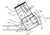
도1a 및 1b는 각각 본 발명의 일 실시예의 교시에 따라 구성되고 동작할 수 있는 광학 개구 배율기의 개략적인 측면 및 전면도이다.
도2a 및 2b는 도1a 및 1b의 광학 개구 배율기로부터 도파관의 부분 반사 내부 파셋들(facets)에 대해 전파하는 이미지 광선의 두 가지 가능한 기하학적 구조를 도시하는 개략도이다.
도3은 도1a 및 1b의 광학 개구 배율기의 내부 파셋들과 다양한 반사된 이미지 사이의 각도 연관성의 개략적인 2차원적 투사이다.
도4a 내지 4d는 도1a 및 1b의 다양한 공액 이미지와 광학 개구 배율기에 대한 내부 파셋들에서의 반사 사이의 상호관계를 나타내는 개략적인 등각 투사도이다.
도5a 내지 5d는 도파관의 다양한 초기 광선 방향 및 다양한 기하학적 형태에 대해, 도1a 및 1b의 광학 개구 배율기로부터 2D 도파관을 따라 전파하는 공액 이미지의 다양한 광선 사이의 개략적인 관계도이다.
도6은 본 발명의 또 다른 양태에 따르는 도1a 및 1b의 광학 개구 배율기로부터 2D 도파관에 이미지를 커플링-인하기 위한 결합 반사기 장치의 개략적인 등각 투사도이다.
도7은 도6의 결합 반사기 장치의 변형된 구현 예이다.
도8a 및 8b는 결합 반사기 장치가 결합 프리즘의 일부로서 구현되는 도6과 동등한 도파관 및 결합 반사기 장치의 상이한 관점에서 본 등각 투사도이다.
도9a 및 9b는 각각 결합 프리즘의 변형 구현예를 나타내는, 도8a 및 8b와 유사한 도면이다.
도10a-10c는 각각 결합 프리즘 및 2D 도파과의 다른 구현예의, 등각 투사도, 상면도 및 측면도이다.
도11, 12 및 13a는 도10a의 결합 프리즘 및 2D 도파관의 또 다른 구현예의 등각 투사도이다.
도13b는 도13a의 결합 프리즘 및 2D 도파관의 상면도이다.
도14a 내지 14c는 본 발명의 또 다른 양태에 따르는 도10a의 결합 프리즘 및 2D 도파관 제조 도중의 3단계의 개략적인 등각 투사도이다.
도15는 본 발명의 또 다른 양태에 따르는 2D 도파관과 이미지 투사 장치의 통합을 도시하는 개략적으로 측면도이다.
도16 및 17은 도15의 통합된 이미지 투사 장치 및 2D 도파관의 두 가지 변형 구현예를 도시하는 개략적인 측면도이다.
도18은 도15-17의 원리의 예시적인 구현예의 3차원 등각 투사도이다.
도19a-19c는 각각 본 발명의 또 다른 구현예에 따르는 2D 도파관과 1D 도파관 사이의 변형 결합 구조를 도시하는, 개략적인 등각 투사도, 측면도, 및 상면도이다.
도20은 도19a-19c의 광학 개구 배율기에 대한 내부 파셋들에서의 반사 민 다양한 공액 이미지 사이의 상호관계를 나타내는 개략적인 등각 투사도이다.
도21a-21c는 본 발명의 교시에 따르는 2D 도파관과 1D 도파관 사이의 결합 구조의 3가지 변형 구현예를 도시하는 등각 투사 측면도이다.
도22a 및 22b는 본 발명의 구현예에 따르는 1D 도파관에 대해 비스듬한 각도로 있는 2D 도파관 사이의 결합 구조의 또 다른 변형 구현예를 각각 도시하는, 개략적인 등각 투사도 및 측면도이다.
도22c 내지 22e는 다양한 변형 구현예를 도시하는 도22b와 유사한 개략적인 측면도이다.
도23은 도1a와 유사하지만 두 도파관 사이에 삽입된 굴절 층을 이용하는 광학 개구 배율기의 개략적인 측면도이다.
도24는 도23의 디바이스에 대한 관련 각도 관계를 도시하는 도3과 유사한 도면이다.
도25a 내지 25c는 두 도파관의 기계적 상호연결을 위한 다양한 구현예를 도시하는 도1a의 것과 유사한 디바이스의 측면도이다.
도25d는 두 도파관의 기계적 상호연결을 위한 구현예를 도시하는 도22e의 것과 유사한 디바이스의 측면도이다.
도26은 제2 도파관에서의 이미지 전파 방향과 제1 도파관 사이의 상대적인 기울기를 도시하는 도1b의 것과 유사한 디바이스의 정면도이다.
도27은 두 세트의 세장형 평행 외부 면에 대해 비스듬하게 경사진 내부 부분 반사 파셋들을 구비한 2D 도파관의 구현예를 도시하는 개략적인 등각 투사도이다.
도28 및 29a는 각각 제1 및 제2 내부 파셋 방향으로 도27의 2D 도파관을 이용하는 디바이스의 두 개의 예시적인 구현예에 대한 기하학적 각도 관계를 도시하는 도3과 유사한 도면이다.
도29b는 도29a의 구현예에 따르는 2D 도파관내에서의 이미지 전파 각도의 개략적인 등각 투사도이다.
도30은 균일성 개선을 제공하기 위해 하나의 인접한 도파관과 중첩되는 본 발명의 또 다른 양태에 따르는 도파관의 개략적인 정면도이다.
도31a 및 31b는 본 발명의 또 다른 양태에 따르는 이미지 균일성에 대한 내부 파셋 간격 변화의 영향을 도시하는 도파관의 개략적인 도면이다.
도31c는 이미지 균일성을 개선하기 위한 다중-경로 구현예를 도시하는 도1b의 것과 유사한 시스템의 정면도이다.
도32a 및 32b는 도1b의 것과 유사한 시스템의 두 개의 또 다른 변형 다중-경로 구현예이다.
도33a는 낮은 각도의 입사 광선을 선택적으로 반사시키도록 코팅된 내부 파셋들을 이용하는 도1b와 유사한 디바이스의 또 다른 구현예의 개략적인 정면도이다.
도33b는 도33a의 광학 개구 배율기의 내부 파셋들과 다양한 반사된 이미지 사이의 각도 관계를 도시하는 도3과 유사한 도면이다.
도33c는 도34a의 디바이스에 사용되는 코팅된 파셋들에 대한 S 및 P 편광된 방사선에 대한 반사성의 각도 의존성을 예시하는 그래프이다.
도34a 내지 34e는 본 발명이 일 양태에 따르는 2D 도파관과 결합 프리즘의 제조 단계에서의 순서를 도시하는 개략적인 등각 투사도이다.
도35a 및 35b는 직접 관찰되는 장면의 투과도의 강도에 대한 본 발명의 일 실시예의 잠재적인 영향을 각각 도시하는 개략적인 정면 및 측면도이다.
도35c 및 35d는 본 발명의 또 다른 양태에 따르는 투과도 강도 수정을 도시하는 도35a 및 35b와 유사한 도면이다.1A and 1B are schematic side and front views, respectively, of an optical aperture multiplier constructed and operable in accordance with the teachings of one embodiment of the present invention.
2a and 2b are schematic diagrams illustrating two possible geometries of an image ray propagating from the optical aperture multiplier of FIGS. 1a and 1b to the partially reflective inner facets of the waveguide.
Figure 3 is a schematic two-dimensional projection of the angular relationship between the inner facets of the optical aperture multiplier of Figures 1a and 1b and various reflected images.
4A-4D are schematic isometric views showing the correlation between the various conjugated images of FIGS. 1A and 1B and reflections at internal facets for an optical aperture multiplier.
Figures 5a to 5d are schematic diagrams of the relationship between various rays of a conjugated image propagating along a 2D waveguide from the optical aperture multiplier of Figures 1a and 1b, for various initial ray directions and various geometries of the waveguide.
Figure 6 is a schematic isometric view of a coupled reflector device for coupling-in an image from the optical aperture multiplier of Figures 1A and 1B to a 2D waveguide in accordance with another aspect of the present invention.
Fig. 7 is a modified implementation of the coupled reflector device of Fig. 6;
8A and 8B are isometric views from different perspectives of a waveguide and coupling reflector device equivalent to that of FIG. 6, in which the coupling reflector device is implemented as part of a coupling prism.
Figures 9a and 9b are views similar to Figures 8a and 8b, each showing an alternative embodiment of a coupling prism.
10A-10C are isometric, top, and side views of another embodiment of a coupling prism and 2D waveguide, respectively.
11, 12 and 13a are isometric views of another embodiment of the coupling prism and 2D waveguide of FIG. 10a.
Fig. 13b is a top view of the coupling prism and 2D waveguide of Fig. 13a.
14a-14c are schematic isometric views of three stages during fabrication of the coupling prism and 2D waveguide of FIG. 10a in accordance with another aspect of the present invention.
Fig. 15 is a schematic side view illustrating the integration of a 2D waveguide and an image projection device according to another aspect of the present invention.
16 and 17 are schematic side views illustrating two variant implementations of the integrated image projection device and 2D waveguide of FIG. 15;
Fig. 18 is a three-dimensional isometric view of an exemplary implementation of the principles of Figs. 15-17;
19a-19c are schematic isometric, side, and top views, respectively, illustrating a strain coupling structure between a 2D waveguide and a 1D waveguide according to another embodiment of the present invention.
Fig. 20 is a schematic isometric view showing the correlation between various conjugated images with reflections at inner facets for the optical aperture multiplier of Figs. 19a-19c.
21A-21C are isometric side views illustrating three variant implementations of a coupling structure between a 2D waveguide and a 1D waveguide according to the teachings of the present invention.
22A and 22B are schematic isometric and side views, respectively, illustrating another modified embodiment of a coupling structure between a 2D waveguide at an oblique angle to a 1D waveguide according to an embodiment of the present invention.
Figures 22c-22e are schematic side views similar to Figure 22b illustrating various alternative implementations.
Fig. 23 is a schematic side view of an optical aperture multiplier similar to Fig. 1A but using a refractive layer sandwiched between two waveguides.
Fig. 24 is a view similar to Fig. 3 showing the relative angular relationships for the device of Fig. 23;
25a-25c are side views of a device similar to that of FIG. 1a showing various implementations for mechanical interconnection of two waveguides.
Fig. 25d is a side view of a device similar to that of Fig. 22e showing an implementation for mechanical interconnection of two waveguides.
FIG. 26 is a front view of a device similar to that of FIG. 1B showing the relative slope between the first waveguide and the direction of image propagation in the second waveguide.
Fig. 27 is a schematic isometric view illustrating an implementation of a 2D waveguide with inner partially reflective facets inclined at an angle to two sets of elongated parallel outer faces.
28 and 29a are diagrams similar to those of FIG. 3 showing geometrical angular relationships for two example implementations of a device using the 2D waveguide of FIG. 27 in first and second inner facet directions, respectively.
Fig. 29B is a schematic isometric view of an image propagation angle in a 2D waveguide according to the embodiment of Fig. 29A.
Figure 30 is a schematic front view of a waveguide according to another aspect of the present invention overlapping with one adjacent waveguide to provide uniformity improvement.
31A and 31B are schematic diagrams of a waveguide showing the effect of varying inter-facet spacing on image uniformity according to another aspect of the present invention.
Fig. 31c is a front view of a system similar to that of Fig. 1b showing a multi-pass implementation for improving image uniformity.
32a and 32b are two other modified multi-path implementations of a system similar to that of FIG. 1b.
Fig. 33A is a schematic front view of another embodiment of a device similar to Fig. 1B that utilizes internal facets coated to selectively reflect low angle incident light rays.
Fig. 33b is a view similar to Fig. 3 showing the angular relationship between the inner facets of the optical aperture multiplier of Fig. 33a and various reflected images.
FIG. 33c is a graph illustrating the angular dependence of reflectivity for S and P polarized radiation for coated facets used in the device of FIG. 34a.
34A to 34E are schematic isometric views showing the sequence in the fabrication steps of a 2D waveguide and coupling prism according to one aspect of the present invention.
35A and 35B are schematic front and side views, respectively, illustrating the potential effect of one embodiment of the present invention on the intensity of transmittance of a scene being directly viewed.
35c and 35d are views similar to FIGS. 35a and 35b illustrating transmission intensity modification according to another aspect of the present invention.
본 발명은 직사각형 도파관을 포함하는 광학 개구 배율기이다.The present invention is an optical aperture multiplier comprising a rectangular waveguide.
본 발명에 따르는 광학 개구 배율기의 원리 및 동작은 도면 및 첨부된 설명을 참고로 이해될 수 있을 것이다.The principle and operation of the optical aperture multiplier according to the present invention will be understood with reference to the drawings and accompanying description.
도면을 살펴보면, 도1a 내지 35는 본 발명의 특정 싱시예에 따라 구성되고 동작하는 광학 개구 배율기의 다양한 양태를 도시한다. 일반적인 용어에서, 본 발명의 일 실시예에 따르는 광학 개구 배율기는 여기에 "x-축"에 대응하는 것으로 임의로 도시된 신장 방향을 갖는 제1 광 도파관(10)을 포함한다. 제1 광 도파관(10)은 직사각형 단면을 형성하는 제1 및 제2 쌍의 평행면(12a, 12b, 14a, 14b)을 갖는다. 본 발명의 특히 바람직한 특정 실시예에 따르면, 여기에서 "파셋(facets)"이라고 불리는, 다수의 내부 부분 반사 표면(40)은 적어도 부분적으로 제1 광 도파관(10)을 신장 방향으로 비스듬한 각도(즉, 평행도 아니고 수직도 아닌)로 가로지른다.Turning to the drawings, FIGS. 1A-35 illustrate various aspects of an optical aperture multiplier constructed and operative in accordance with certain embodiments of the present invention. In general terms, an optical aperture multiplier according to an embodiment of the present invention includes a first
광학 개구 배율기는 또한 바람직하게는 제1 광 도파관(10)과 광학적으로 결합되고, 평판형(slab-type) 도파관을 형성하는 제3 쌍의 평행면(22a, 22b)을 갖는, 제2 광 도파관(20)을 포함하는데, 즉, 도파관의 다른 두 차원(dimension)은 제3 쌍의 평행면(22a, 22b) 사이의 거리보다 적어도 큰 크기의 순서이다.The optical aperture multiplier is also preferably optically coupled with the first
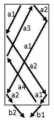
도파관 사이의 광학적 결합, 및 다수의 반사 표면(40, 45)의 배치 및 구성은, 이미지가 제1 및 제2 쌍의 평행면(12a, 12b, 14a, 14b) 모두에 비스듬한 결합 각도에서 초기 전파 방향(30)으로 제1 광 도파관(10) 안에 결합될 때, 이미지는 부분 반사 표면(40)에서 반사된 이미지의 강도의 비율로 제1 광 도파관(10)을 따라 4-접(four-fold) 내부 반사(이미지(a1, a2, a3, a4) 만큼 전진하여 제2 광 도파관(20)에 커플링-인된 다음, 사용자의 눈(47)으로 보이는, 가시 이미지(c)로서 평행 면 중 하나로부터 외부로 향하도록 부분 반사 표면(45)에서 반사된 이미지의 강도의 비율로 제2 광 도파관(20) 내의 2-접(two-fold) 반사(이미지(b1, b2))를 통해 전파한다.The optical coupling between the waveguides, and the arrangement and configuration of the plurality of
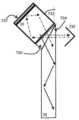
도1a 및 1b를 더욱 구체적으로 살펴보면, 이것은 상기 설명의 일 구현예의 첫번째 실례를 나타낸다. 제1 도파관(10)은 두 세트의 평행 면사이의 반사에 의해 두 차원(dimension)으로 투입된 이미지를 안내한다는 점에서 2D 도파관으로서 불리지만, 제2 도파관(20)은 한 쌍의 평행 면 사이의 오직 한 차원으로 투입된 이미지를 안내하는 1D 도파관으로 불린다. 광학 이미지 발생기(도시되지 않음)로부터의 광속(light beam)은 제1 도파관(102) 안으로 비스듬하게 투입된다. 결과적으로, 광은 도1a의 측면도에 도시된 바와 같이 도파관의 네 개의 외부 면 전부로부터 반사되는 동안 도파관(10)을 따라 전파된다. 이 과정에서, 면들에 의해 내부적으로 반사되는 것과 동일한 이미지를 나타내는 네 개의 공액 빔 벡터(a1, a2, a3, a4)가 생성된다.Looking more specifically at FIGS. 1A and 1B , this represents a first example of one embodiment of the description above. The
도파관(10) 안으로 투입되는 빔(30)의 각도는 이 도파관의 네 개의 내부 면 모두로부터 반사되도록 설정된다. 이 광속은 제1 도파관(10)의 바닥면(12b), 즉 제2 도파관(20)에 인접한 면으로부터, 낮은 각도로 반사되어야 하고, 제1 도파관(10)으로터 제2 도파관(20)으로 가파른 각도로 전파되어야 한다. 이 속성은 전체 내부 반사에 의해 또는 광학적 코팅에 의해 달성될 수 있다. 회절 패턴은 동일한 표면상의 회절과 투과를 결합함으로써 이 광학 속성을 수행할 수 있다. 제1 도파관(10)의 다른 3개의 면(12a, 14a, 14b)로부터의 반사는 동일한 방식으로 또는 반사 코팅을 사용하여 발생할 수 있다.The angle of the
제1 도파관(10) 내에서 안내된 광속의 일부(예를 들어 a1 및 a2)는 제2 도파관(20)의 입력 결합 표면상에 하방으로 내부 평행 부분 반사기(파셋, 40)에 의해 반사된다. 제2 도파관(20)에서, 이 광속들은 b1 및 b2로 규정된다.A portion of the luminous flux guided in the first waveguide 10 (eg a1 and a2) is reflected by an internal collimated partial reflector (facet) 40 downward onto the input coupling surface of the
광속(b1 및 b2)은 외부 면에 의해 반사되고 결합하게 되는데, 즉, 광속(b1)은 반사되어 광속(b2)이 되고 반대로 광속(b2)은 반사되어 광속(b1)이 된다(도1a에 도시된 바와 같이). 제1 도파관(10)의 외부 전방 및 후방 면(14a, 14b)은 서로에 대해, 및 이 구현예에서 제2 도파관(20)의 대응하는 외부 면(22a, 22b)에 대해 평행이어야 한다. 평행으로부터 벗어남은 결합된 이미지(b1 및 b2)가 정확한 공액 이미지가 되지 않게 할 것이며, 이미지 품질은 저하될 것이다.The beams b1 and b2 are reflected by the outer surface and combined, that is, the beam b1 is reflected to become the beam b2 and vice versa, the beam b2 is reflected to become the beam b1 (see Fig. 1a). as shown). The outer front and back faces 14a, 14b of the
제2 도파관(20)내의 외부 파셋(45)은 광속(b2)을 도파관 외부로 및 관찰자(47)의 눈 안으로 반사한다.The
도파관(10 및 20)의 내부 파셋에 의한 반사 과정은 도2a 및 2b에서 추가로 설명된다. 두 개의 기본 구성이 그려져 있으며, 광속 및 파셋의 상대 각도에 의해 구별된다. 이 개략적인 도면에서, 해당 도파관의 측면도로부터 관찰되는 것처럼 동일한 기하학적 고려사항이 각각 적용되기 때문에 광속(a1, a2, b1)은 동일한 벡터(기준은 오직 b1일 것이다)로 도시된다. 광속(a3, a4, b2)도 동일한 벡터(기준은 오직 b2일 것이다)로 도시된다.The process of reflection by the inner facets of
광속(b2)은 실제로는 도2a에서 두 개의 벡터로 도시된 것처럼 동일한 방향으로 전파하는 광선 다발이다. 이 경우, 하나의 벡터는 외부면에 의해 반사되어 b1이 되어 내부 파셋(40)(또는 파셋(45)) 상에 놓이고 그 중의 일부는 c1으로 반사된다. 다른 b2 벡터는 파셋에 의해 벡터 c2로 직접 반사된다. 벡터들(c1 및 c2)은 반드시 이 순서대로 정상 이미지(normal image) 및 고스트 이미지(ghost image)를 나타내지는 않는다. 이 구성에서, b1 및 b2는 동일한 측면으로부터 파셋(45)상에 충돌한다.The luminous flux b2 is actually a bundle of rays propagating in the same direction as shown by the two vectors in Fig. 2a. In this case, one vector is reflected by the outer surface as b1 and lies on the inner facet 40 (or facet 45), some of which is reflected as c1. The other b2 vector is reflected directly by the facet into vector c2. Vectors c1 and c2 do not necessarily represent a normal image and a ghost image in this order. In this configuration, b1 and b2 impinge on
덧붙여서, 이미지가 광속으로 표현되는 어디에서든, 광속은 이미지의 샘플 광속이며, 일반적으로 이미지의 점 또는 픽셀에 각각 대응하는 약간 다른 각도로 다중 빔으로 형성된다는 것을 주목해야 한다. 특별히 이미지의 말단이라고 언급되는 경우를 제외하고, 도시된 광속은 일반적으로 이미지의 중심이다.In addition, it should be noted that wherever an image is expressed as a flux of light, the flux of light is a sample flux of light in the image, usually formed by multiple beams at slightly different angles, each corresponding to a point or pixel in the image. Except where specifically referred to as the end of the image, the luminous flux shown is generally the center of the image.
도2b는 본질적으로 동일한 과정이지만 b1 및 b2가 대향 측면으로부터 파셋(40(또는 45))상에 충돌하는 기하학적 구조를 설명한다.Figure 2b illustrates essentially the same process, but with geometry where b1 and b2 impinge on facets 40 (or 45) from opposite sides.
두 경우, S 및 P 편광의 이미지(c1 및 c2)에 대한 반사의 크기는 이 파셋 상의 코팅에 의해 결정된다. 바람직하게는 하나의 반사는 이미지이고 나머지 하나는 그것이 원치않는 "고스트" 이미지에 해당하기 때문에 억제된다(suppressed). 어느 범위의 입사 빔 각도가 반사되고 어느 범위의 입사 빔 각도가 투과되는지를 컨트롤하기 위해 적합한 코팅은 당업계에 공지되어 있으며, 본 발명에 공동양도된, 미국특허 제93911573호 및 제7457040호에 상세하게 설명된 것을 알 수 있다.In both cases, the magnitude of the reflection for images c1 and c2 of S and P polarization is determined by the coating on this facet. Preferably one reflection is an image and the other is suppressed because it corresponds to an unwanted "ghost" image. Coatings suitable for controlling which ranges of incident beam angles are reflected and which ranges of incident beam angles are transmitted are known in the art and are detailed in US Pat. Nos. 93911573 and 7457040, commonly assigned herein. It can be seen that described
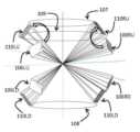
"고스트" 이미지가 메인 또는 공액 이미지(c1 및 c2 중첩)와 중첩되지 않도록 시스템을 디자인하는 것이 특히 바람직하다. 도파관 내의 이미지 전파를 위한 TIR(total internal reflection, 내부 전반사) 조건을 유지하는 동시에 고스트-오버랩을 피하면서 빔의 적합한 각도를 디자인하는 과정은 도3에서 설명된다. 이 도면은 이 발명의 현재 추가적인 실시예 이후로 추가로 사용될 개략적인 표현을 도입한다.It is particularly desirable to design the system so that the "ghost" images do not overlap with the main or conjugate images (overlapping c1 and c2). A process of designing a suitable angle of a beam while maintaining total internal reflection (TIR) conditions for image propagation in a waveguide while avoiding ghost-overlap is described in FIG. 3 . This figure introduces a schematic representation that will be further used on and on from present further embodiments of this invention.
따라서, 도3은 직선 축을 따르는 거리에서 회전이 도시되는 도파관(10 및 20)의 기하학적 형상의 투사를 도시한다. 도표는 따라서 직교좌표의 구면 좌표계를 나타낸다. 이 표현은 다양한 왜곡을 가져오고, 상이한 축을 따르는 변위(displacements)는 비-교환적이다(상이한 축에 대한 회전의 특성처럼). 그럼에도 불구하고, 이 도표 형태는 설명을 단순화하기 위해 발견되었으며 시스템 디자인을 위한 유용한 도구를 제공한다. 설명을 위해, X, Y, 및 Z 축을 따르는 방향은 한 번의 회전 순서에 따라 표시된다.Accordingly, Figure 3 shows a projection of the geometry of
큰 원은 도파관의 다양한 외부 면의 임계 각도(내부 전반사(TIR)의 경계)를 나타낸다. 따라서, 원 밖의 한 점은 TIR에 의해 반사될 빔의 각도 방향을 나타내지만, 원 안의 한 점은 면을 통과하여 도파관 밖으로 투과될 빔을 나타낸다. 원(57 및 59)은 도파관(10)의 전방 및 후방 외부 면(14a 및 14b)의 임계각도 및 도파관(20)의 전방 및 후반 외부 면(22a 및 22b)의 임계 각도를 나타낸다. 마주보는 파셋의 원 사이의 "거리"는 180도이다. 원(61 및 63)은 도파관(10)의 상단 및 하단 외부 면(12a 및 12b)의 임계 각도를 나타낸다. 일점 쇄선(doted-dashed line, 65 및 67)은 도파관의 이 외부 면들의 방향을 나타낸다.The large circles represent the critical angles (the boundaries of total internal reflection (TIR)) of the various outer faces of the waveguide. Thus, a point outside the circle represents the angular direction of the beam to be reflected by the TIR, while a point inside the circle represents the beam to pass through the plane and out of the waveguide.
전술된 바와 같이, 내부 반사를 경험하는 동안 도파관 안으로 이미지가 주입된다. 이어지는 예에서, 모든 반사는 TIR 기반이며, 따라서 주입된 이미지(a1)는 도3에서 임의의 원 밖에 존재하는 것으로 도시된다. 각도 공간의 사각형 이미지는 사각형 형상을 갖는다.As described above, an image is injected into the waveguide while experiencing internal reflection. In the examples that follow, all reflections are TIR-based, so the injected image a1 is shown outside the random circle in FIG. 3 . A rectangular image in angular space has a rectangular shape.
이미지(a1)가 도파관(10)의 외부 면(12a, 12b, 14a, 14b)으로부터 반사되면(방향 65 및 67로 표시됨), a2, a3, a4로 배가되어(multiplied) a1으로 돌아간다(네 개의 구부러진 실선에 의해 개략적으로 표시됨). 모든 이미지의 반사는 이미지 자체와 동일하지만, 다른 한편으로는 반사 각도가 입사 각도와 동일하다는 광학 원리에 따라, 각각의 면(선 65 및 67)으로부터의 각도 "거리"를 갖는다.When image a1 is reflected from
내부 파셋(40)의 배향(orientation)(도1b의)은 여기에서 파셋의 각도 경사에 따라 배치되는 선(70)으로 그려진다. 이미지(a1 또는 a2)가 파셋(70)(40)을 만나면, 이미지(a1 또는 a2)는 이미지(b1, b2)에 각각 파선 화살표로 그려진 바와 같이 선(70)으로부터 맞은편의 동일한 각도 거리까지 반사된다.The orientation of the internal facets 40 (in Fig. 1b) is here drawn with
b1 및 b2는 제1 도파관(10)의 하단 외부 면의 임계 각 경계(61) 내에 존재하기 때문에, 이 도파관으로부터 커플링-아웃되고 제2 도파관(20)에 커플링-인될 것이다.Since b1 and b2 are within the
이미지(b1 및 b2)가 도파관(20) 내에서 전파되면 각도 배향성(67)을 갖는 전방 및 후방 외부 면(22a 및 22b)으로부터의 반사에 의해 상호 교환된다(반사는 곡선형 실선의 이중 화살표로 그려짐).As the images b1 and b2 propagate within the
마지막으로, 이미지(b1)는 배향(72)에서 내부 파셋(45)을 만나고(도1a) 이미지(c)로 반사된다. 이미지(c)는 임계 각도 원(57)내에 존재하기 때문에, 제2 도파관(20)으로부터 커플링-아웃되어 눈(도1a의 47)에 결합된다.Finally, image b1 meets
이 모든 구성에서, 이렇게 교차하는 것은 "고스트" 이미지가 정상 이미지에 중첩되게 하기 때문에, 내부 파셋(70 및 72)의 각도는 이미지의 각도 형상(정사각형)을 교차하지 않아야 한다.In all of these configurations, the angles of the
이미지(c)는 도3에 예시된 바와 같이, 도파관(20)에 대해 임의의 각도로(반드시 수직일 필요는 없다) 빠져나오도록(emerge) 설계될 수 있는데, c는 z 방향의 중심에 있지 않다.Image c can be designed to emerge at any angle (not necessarily perpendicular) to the
파셋(40 및 45)에는 바람직하게는 낮은 각도 이미지(a3, a4, b2)를 각각 감소시키거나 실질적으로 제거하는, 전술된 바와 같은, 코팅이 제공된다.
도3에 도시된 계산 과정은 표현의 용이성 및 명확성을 위한 2D 직교 좌표계로 개략적으로 도시되어 있다. 최종적인 정확한 디자인의 시스템은 도4a 내지 4d에 도시된 바와 같이 구면 좌표계에서 수행된다. 도4a는 이미지 a1 내지 a4 사이의 결합을 나타낸다. 도4b는 파셋(40)상의 반사에 의해 a1을 b1에, a2를 b2에 결합하는 것을 도시한다. 도4c는 제2 도파관(20)에서 b1과 b2 사이의 결합을 나타낸다. 도4d는 파셋(45)상의 반사에 의해 b1으로부터 c로 결합하는 것을 나타낸다.The calculation process shown in Figure 3 is schematically illustrated in a 2D Cartesian coordinate system for ease and clarity of expression. The final accurate design of the system is performed in spherical coordinates as shown in Figures 4a to 4d. Figure 4a shows the coupling between images a1 to a4. Figure 4b shows the coupling of a1 to b1 and a2 to b2 by reflection on
도파관(10) 내의 내부 반사 도중에, 도5a 내지 5d에 도시된 바와 같이 라운드트립(roundtrip) 당 모든 차원(y 또는 z)에서 임의의 수의 반사가 존재할 수 있다. 도5a는 외부 면 당 하나의 반사를 묘사한다. 이 상태에서 b1은 a1에 의해 시작된다. 그러나, 상이한 이미지 필드의 다양한 광속은 상이한 각도를 갖기 때문에, 결국 반사의 배향은 빔이 도파관(10)의 x 축을 따라 전파할 때 변경될 수 있다. 도5b는 a2에 의해 생성되는 b2로 결과를 이끌어낼 수 있는 상이한 배향을 나타낸다. 따라서, 모든 디자인에서 b1 및 b2의 생성이 모두 가정되어야 한다. 도파관(10)의 종횡비는 도5c에 그려진 바와 같이 외부 파셋 당 한번 이상의 반사를 갖도록 디자인될 수 있다. 상이한 필드 각도에 대해, 반사의 배향은 도5d에 도시된 바와 같이 변할 수 있다. 실제로, 본 발명의 어떤 특히 바람직한 구현예는 이하 논의되는 바와 같이, 경로 중 하나를 억제하도록 특별한 주의사항이 취해지는 경우를 제외하고, 두 이미지(a1 및 a2)는 항상 결합 해제되어(out-coupled) b1 및 b2를 만들도록, 도파관(10)이 모든 네 개의 공액 이미지(a1-a4)로 체적적으로(volumetrically) 채워지도록 보장한다.During internal reflections in
도파관(10 및 20)의 외부 면과 내부 파셋에 의한 조합된 반사는 원래 주입된 개구를 x 및 y 차원 모두로 연장시킨다. 도파관(10)은 x 차원으로 개구를 연장시키고 도파관(20)은 y 차원(도1b에서처럼 표시되는 축)으로 개구를 연장시킨다. 제1 도파관(10)의 개구 연장은, 이하 모두 상세히 논의되는 것처럼, 바람직하게는 이미지로 도파관을 채우고 도파관의 길이를 따라 연속적인 방식으로 파셋을 거쳐 도파관 밖으로 이미지를 커플링-아웃함으로써 달성된다.The combined reflection by the outer facets and inner facets of
커플링-인 장치(coupling-in arrangements)Coupling-in arrangements
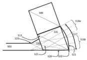
연장된 개구를 가로질러 균일한 강도를 획득하기 위해, 빔의 주입된 추기 개구는 균일해야 하고 도파관을 "채워야(fill)" 한다. 용어 "채우다(fill)"은 이미지의 각각의 점(픽셀)에 해당하는 광선이 도파관의 전체 단면을 가로질러 존재한다는 것을 표시하기 위해 이 문맥에서 사용된다. 개념적으로, 이 속성은, 도파관(10)이 임의의 점에서 횡방향으로 절단된 경우, 및 핀홀(pinhole)을 구비한 투명 시트가 절단 단부상에 배치되는, 핀홀은 단면을 가로질러 어디든지 배치될 수 있으며 완전한 투사 이미지를 야기할 것이라는 것을 의미한다. 실제로, 2D 도파관(10)에 대해, 4개의 완전한 이미지(a1, a2, a3, a4)의 투사를 초래하고, 그 중 a2 및 a4는 반전된다(inverted).To achieve uniform intensity across the elongated aperture, the beam's injected extraction aperture must be uniform and "fill" the waveguide. The term "fill" is used in this context to indicate that a ray of light corresponding to each point (pixel) in the image exists across the entire cross-section of the waveguide. Conceptually, this property is such that if the
입력된 이미지로 도파관을 채우는 것을 보장하기 위해, 약간 큰 크기의 입력 이미지는 도파관으로 들어갈 때의 크기로 잘려야(trim) 한다. 이것은 배가된(multiplied) 인접 구경이 한편으로는 중첩되지 않으며 다른 한편으로는 간극을 갖지 않도록 보장한다. 자르기(trimming)는 광속이 도파관 안에 주입될 때 수행된다.To ensure that the input image fills the waveguide, a slightly oversized input image must be trimmed to the size it enters the waveguide. This ensures that the multiplied adjacent apertures on the one hand do not overlap and on the other hand do not have gaps. Trimming is performed when the light flux is injected into the waveguide.
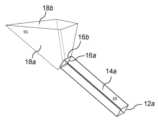
제1 도파관(10)에 효과적인 이미지 커플링-인을 달성하기 위한 다수의 구성이 도6 내지 13b에 도시된다. 먼저 도6 및 7을 참조하면, 이들은 제1 도파관(10)을 균일하게 채우기 위해 입력 이미지를 자르기 위한 커플링-인 장치의 자유-공간 거울 구현 예를 개략적으로 도시한다. 이 경우, 면(12a)은 제1 근위 에지(16a)에서 종료되고 면(14a)은 제2 근위 에지(16b)에서 종료된다. 도파관을 완전히 채우기 위해, 광학 개구 배율기가 제1 도파관(10)과 일체로 형성되거나 제1 도파관(10)과 광학적으로 결합되는 결합 반사기 장치를 포함하는 것이 본 발명의 특정 실시예의 특히 바람직한 특성이다. 결합 반사기 장치는 표면(12b)의 폭보다 큰 신장(elongation)의 방향에 대해 수직인 폭을 갖는, 면(12b)의 근위 연장으로서(도6), 또는 면(12b)에 평행이고 외부의 반사기로서(도7) 배치된 제1 반사기(18a)를 포함한다. 결합 반사기 장치는 또한 표면(14b)의 폭보다 큰 신장의 방향에 대해 수직인 폭을 갖는, 면(14b)의 근위 연장으로서(도6), 또는 면(14b)에 대해 평행이고 외부의 반사기로서 배치된 제2 반사기(18b)를 포함한다. 이 결합 반사기 장치의 결과로서, 이미지가 도입되는 광 입력 축을 따라 볼 때(도6 및 7의 관점), 제1 및 제2 근위 에지(16a 및 16b)는 물리적 개구의 4배(2x2)인 외관상(apparent) 개구에 전체적으로 해당하는, 제1 및 제2 근위 에지 및 결합 반사기 장치에서 반사된 제1 및 제2 근위 에지의 이미지들에 의해 경계가 지어진 외관상 도파관 개구를 제시한다. 결합 반사기가 도파관의 면들에 대해 외부에 놓이는 경우, 외관상 개구는 물리적 개구 자체로부터 약간 이격된 물리적 개구의 3개 이미지로 구성되며, 각각의 개구는 물리적 개구의 4개 에지 모두에 의해 만들어진다. 이것은 개구 사이의 "공간"에서 떨어지는 이미지 강도로 인해 약간 비효율적이지만, 개구를 채우는 것은 여전히 달성된다.A number of configurations for achieving effective image coupling-in to the
여기에 도시된 바와 같은 하나의 바람직한 기하학적 구조에서, 광 입력 축은 제1 및 제2 반사기(18a 및 18b) 모두에 대해 비스듬하다. 이 도면들에서 분명히 볼 수 있듯이, 반사기가 도파관의 것보다 큰 차원을 갖도록 하는 요구사항은 여기에서 이미지의 클리핑 및 도파관의 불완전한 채움이 발생하지 않도록 보장하기 위해 요구된다. 이 방식으로, 도파관은 그 전체 단면을 가로질러 모두 4개의 이미지로 확실하게 채워진다.In one preferred geometry, as shown here, the light input axis is oblique for both first and
자유 공간 거울의 사용이 일부 경우 실현 가능하지만, 도파관(10)과 일체로 형성되거나 광학적으로 결합된 결합 프리즘으로서 결합 반사기 장치를 구현하는 것이 일반적으로 유리하며, 제1 및 제2 반사기(18a 및 18b)는 결합 프리즘(91)의 면에 의해 제공된다. 결합 프리즘의 다른 면은 바람직하게는 이미지가 도입되는 광 입력 축에 일반적으로 수직인 결합 표면을 제공한다. 이러한 장치의 예는 도8a 내지 8b 및 9a 내지 9b에 도시되어 있으며, 도8a 내지 8b는 도6와 기하학적으로 동일하고 도9a 내지 9b는 도7과 기하학적으로 동일하다. 이 경우, 도파관(10)의 근위 "에지"는 도파관 표면과 결합 프리즘의 교차에 의해 규정된 에지이다. 이 경우, 다른 인접하는 표면은 바람직하게는 그 근위 에지 외부로 떨어지는 광이 도파관에 들어가지 않는 방향으로 반사(또는 투과)될 수 있도록 외부로 경사진다. 선택적으로, 빗나간(stray) 방사선이 원하지 않는 위치에 도달하는 것을 추가로 막기 위해 이 표면들에 흡수성 물질이 도포된다.Although the use of free space mirrors is feasible in some cases, it is generally advantageous to implement the coupling reflector arrangement as a coupling prism integrally formed with or optically coupled to the
커플링-인 기하구조의 또 다른 예는 도10a 내지 10c에 도시되어 있으며, 도파관에 대한 이미지의 커플링-인 도중에 샘플 파면의 진행을 더욱 상세하게 설명한다. 이 경우, 빔(30)은 도10b에 도시된 바와 같이, x-축을 따라 측정될 때 임의의 초기 개구 측방향 차원(81)을 가지고 주입된다. 이 개구의 전방 단부는 빔이 도파관에 들어갈 때 제1 근위 에지(16a)에 의해 잘린다. 입사 도중에 일 측면상에서 잘라진 빔 개구는 대향하는 결합 반사기(18a) 및/또는 그 연속 면(12b)에 의해, 그 후방 측면이 동일한 제1 근위 에지(16a)에 의해 한번 더 잘리는, 전방 면(12a)으로 반사된다. 도파관을 따라 빔미 전파될 때, 그 개구(84 및 88)는 이제 중첩 또는 간극 없이 인접하여, 도파관을 채운다.Another example of a coupling-in geometry is shown in FIGS. 10A-10C, illustrating in more detail the progression of the sample wavefront during coupling-in of the image to the waveguide. In this case,
본 발명의 특히 바람직한 구현예에 따르면, 빔 개구의 제2 차원은 제2 근위 에지(16b)에 의해 동시에 잘린다. 근위 에지(16a 및 16b)의 상대적인 배향은 중요하지 않다. 예를 들어, 도10 내지 10cc에서 에지(16a)가 종방향 x-축에 대해 경사진 것으로 도시되어 있지만, 근위 에지(16a 및 16b)가 종방향 x-축에 대해 모두 수직인 도11에 도시된 다른 기하학적 형태는 일부 경우 제작이 단순화된다. 두 근위 에지(16a 및 16b)는 바람직하게는 코너에서 교차하지만, 광학이 충분히 넓어서 금의 에지(16a 및 16b) 및 그 반사에 의해서만 트리밍이 수행되는 한 필수적인 것은 아니다. 교차하지 않는 예는 도12에 도시되어 있다.According to a particularly preferred embodiment of the invention, the second dimension of the beam aperture is simultaneously cut by the second
제1 차원에서의 자르기는 도10b를 참고로 하여 제1 차원에 대해 기재되는 것과 동일한 방식으로 발생한다. 따라서 도10c에서, 초기의 잘리지 않은 투사 이미지 개구는 x-축을 따라 측정될 때 초기 개구 수직 차원(92)을 갖는다. 섹션(91)으로부터 도파관(10) 안으로 경사져서 들어갈 때, 그 전방은 제2 근위 에지(16b)에 의해 잘린다. 빔(92)이 대향 외부 면(14a) 및/또는 그 연속부로부터 반사된 후, 그 뒤쪽은 또한 적절한 크기(94)로 제2 근위 에지(16b)에 의해 잘린다. 결과적으로, 이 차원을 따르는 모든 반사된 개구는 또한 인접해 있다. 두 차원으로의 이 트리밍의 전체적인 결과는 도파관(10)이 반드시 모든 네 개의 이미지/공액 이미지(a1-a4)로 채워져서, 두 차원을 따라 개구의 연속적인 중단없는 연장을 용이하게 한다는 것이다.Cropping in the first dimension occurs in the same way as described for the first dimension with reference to FIG. 10B. Thus in Fig. 10c, the initial uncropped projection image aperture has an initial aperture
끝(stop)(16a, 16b)은 흡수 물질 또는 굴절 물질(프리즘 또는 코팅과 같은)을 사용하여 제조될 수 있다. 예를 들어, 도10 내지 13에서, 진입 광을 분산시키는 역할을 하는 도파관의 입구에서 계단 형태로 그려져 있다.
결합 프리즘(91)은 도파관(10)과 일체로 또는 두 부품을 공지의 기술로 부착함으로써 제조된다. 이 부품들을 부착하기 위한 특정의 특히 바람직한 접근방법은 이하 추가로 설명될 것이다.Coupling
앞서 지적한 바와 같이, 도파관(10)에 커플링-인된 이미지의 광 축은 두 세트의 평행한 면에 대해 비스듬하게 경사진다. 그러나, 예를 들어, x-축에 수직인 광 축을 따라 입력된 광을 반사하도록 배치되어 외관상의 도파관 개구상에 부딪히도록 결합 프리즘(91)의 비스듬한 반사 표면(91a)에서의 추가적인 반사 입력처럼, 이것은, 이미지 전파의 필요한 각도는 다른 광학 부품에 의해 달성될 수도 있기 때문에, 반드시 이미지 프로젝터의 비스듬한 배향을 필요로 하지는 않는다.As previously pointed out, the optical axis of the image coupled-in to the
이러한 옵션은 도13a 및 13b에 도시되어 있으며, 여기에서 비스듬한 반사 표면(91a)이 백 미러(back mirror)를 제공한다. 도13b에 도시된 바와 같이, 임의의(대형) 개구(81)는 16a에 의해 다듬어지는 동안 반사 표면(91a)에 의해 반사되도록 도파관안으로 들어간다. 한 번의 반사(82) 후, 개구의 후방 측은 동일한 에지(16a)에 의해 다듬어진다.This option is shown in Figures 13a and 13b, where an oblique
개구(81)의 나머지 빛은 두 가지 메커니즘을 사용하는 에지(16a)에 의해 다듬어진다 : 입구에서, 나머지 광은 전파를 계속하고 에지(16a) 너머로 외부로 투과하지만, 반사(82에서 84로) 후 파면의 후방 측은 에지의 우측에 있고 따라서 광 외부 또는 관련 이미지의 외부에 경사지게 91a 만큼 한번 더 반사된다.The remaining light in
에지(16b)는 다른 차원에서 이전처럼 수직 축을 다듬기를 계속한다. 선택적으로, 미러(91a)는 두 축에 대해서 기울어져서 입력 이미지(30)가 도파관의 한 면에 수직일 때 이미지의 원하는 전파 방향을 생성하도록 한다. 따라서, 요약하면, 원하는 각도로 도파관에 이미지/빔을 커플링하는 것은 프리즘, 도파관의 전방, 후방 또는 내부에 배치된 미러, 또는 다른 공지된 방법을 사용하여 달성될 수 있다. 이러한 모든 방법은 기재된 이중-정지 구조가 존재하는 한 실현 가능하다.
연장된 개구를 가로질러 균일한 강도를 달성하기 위해, 트리밍 에지(16a 및 16b)는 최소 편차 및 산란을 구비한 깨끗한 에지이어야 하는 것이 바람직하다. 접착제 또는 다른 교란 요소의 잔류물은 균일성의 열화를 초래할 수 있다. 도14a 내지 14c는 깨끗한 트리밍 에지(또는 다른 응용예에서는, 연속적인 외부 표면)의 구성을 용이하게 하는, 광학 소자가 결합되는 다른 상황에서도 적용할 수 있는, 본 발명의 추가 양태를 도시한다. 도파관(10)의 관련 외부 면(12a 및 14b)은 먼저 반사성 또는 보호성 코팅(1610)에 의해 코팅된다. 다음으로 도파관(10)의 에지는 필요한 트리밍 에지(1630)에 따라 연마되고(polished) 마지막으로 프리즘(1640)이 부착된다. 이 부착에서, 두 면(도시된 바와 같은 모양의 후방 측상의)은 이 면들의 연속으로서 결합 반사기를 제공하기 위해 도파관의 외부 표면의 정확한 연속이어야 한다. 이 면들이 연속적이지 않으면, 반사성 코팅(1610)은 바람직하게는 대향 면(12b 및 14a)도 또한 바람직하게 덮어야 한다. 이 접근법은 1D 도파관을 구비한 시스템과도 연관된다. 결합 표면의 각도는 임의의 배향일 수도 있다.In order to achieve uniform intensity across the elongated aperture, the trimming edges 16a and 16b should preferably be clean edges with minimal deviations and scattering. Residues of adhesive or other disturbing elements may lead to degradation of uniformity. 14a-14c illustrate a further aspect of the present invention, applicable in other situations where optical elements are incorporated, which facilitates the construction of a clean trimmed edge (or in other applications, a continuous outer surface). The associated
상기 기술, 즉 두 광학 부품을 결합하기 위해 표면을 마무리하기(finishing) 전에 보호성 유전체 또는 반사성 코팅을 제공하는 것은 여기에 기재된 특정 응용을 넘어서는 광범위한 문제를 다룬다는 점에 주목해야 한다. 구체적으로, 두 부품이 하나에서 다른 곳으로 광학 경로를 제공하도록 결합될 때마다, 부품들은 적합한 광학 접착제에 의해 결합되어야 하며, 전형적으로 부품에 인덱스-매칭된다. 최적의 광학 결합을 보장하기 위해, 전체 인터페이스 표면은 접착제로 완전히 덮여야 한다. 다른 한편으로, 정확하게는 접착제의 원하는 광학적 속성 때문에, 인터페이스로부터 부품의 하나의 외부 표면까지의 접착제의 과잉(overspill)은 전형적으로 부품의 광학적 속성을 손상시킨다. 바람직하게는 인터페이스 표면의 연마 전에, 보호성 코팅으로 인접 표면을 우선적으로 코팅함으로써, 외부 표면상의 접착제의 과잉은 줄어들거나 제거될 수 있다. 결합 후에 특정 표면이 편평하게 되도록 두 부품이 결합되는 경우, 이러한 코팅은 결합 전에 부품 모두에 유리하게 제공될 수 있다. 특정 응용에서, 오직 한 측만, 또는 면의 서브셋을 코팅하는 것은 예를 들어, 특정 표면상의 과도한 접착제다 또 다른 연마 단계에 의한 본딩후에 쉽게 제거될 수 있는 경우, 충분하다.It should be noted that the above technique, ie, providing a protective dielectric or reflective coating prior to surface finishing to join two optical components, addresses a wide range of issues beyond the specific applications described herein. Specifically, whenever two components are joined to provide an optical path from one to the other, the components must be joined by a suitable optical adhesive, typically index-matched to the components. To ensure optimal optical coupling, the entire interface surface must be completely covered with adhesive. On the other hand, precisely because of the desired optical properties of the adhesive, an overspill of adhesive from the interface to one outer surface of the component typically compromises the optical properties of the component. By preferentially coating the adjacent surface with a protective coating prior to polishing the interface surface, excess adhesive on the external surface can be reduced or eliminated. When two parts are joined such that after bonding certain surfaces are flat, such a coating can advantageously be applied to both parts prior to bonding. In certain applications, coating only one side, or a subset of sides, is sufficient, for example, if excess adhesive on a particular surface can be easily removed after bonding by another polishing step.
커프링-인 장치의 상기 구현예는 바람직하게는 외관상 도파관 개구를 완전히 중첩시키도록 광 입력 축을 따라 무한대로 시준되는 이미지를 투사하도록 배치되는 이미지 프로젝터와 함께 사용된다. 임의의 적합한 유형 및 기술의 이미지 프로젝터가 사용될 수 있으며, 다양한 자유-공간 이미지 프로젝터를 포함한다. 어떤 경우, 특히 소형의 튼튼한 구현예를 제공하기 위해, 이미지 프로젝터는 결합 프리즘과 기계적으로 일체화될 것이다(즉, 일체형으로 구성 또는 견고하게 상호연결됨). 이 유형의 다양한 구현예는 도15-18을 참고로 설명될 것이다.This embodiment of the cuffing-in device is preferably used with an image projector arranged to project an image collimated to infinity along the light input axis to completely overlap the waveguide opening in appearance. Any suitable type and technology of image projectors may be used, including a variety of free-space image projectors. In some cases, to provide a particularly compact and robust implementation, the image projector will be mechanically integrated (ie, integrally constructed or rigidly interconnected) with the coupling prism. Various implementations of this type will be described with reference to FIGS. 15-18.
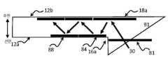
먼저 도15를 살펴보면, 이것은 여기에 503으로 번호 붙여진 2D 도파관의 상황에서 사용하기 위한 PCT 특허공개 WO2015/162611의 소형 이미지 프로젝터의 변화를 도시한다. 소형 이미지 프로젝터는 조명 편광 빔 분리기(Polarizing Beam Splitter, PBS, 500), 시준 PBS(501), 도파관(503)에 커플링-인되는 결합 프리즘(502)(도10a-10c의 91과 동일함)을 포함한다.Turning first to Figure 15, which illustrates a variation of the miniature image projector of PCT Patent Publication WO2015/162611 for use in the context of a 2D waveguide, here numbered 503. The miniature image projector includes an illumination Polarizing Beam Splitter (PBS) 500, a collimating
다음 설명에서, 편광 관리 부품(파장판 및 편광자)은 명확성을 위해 생략된다. 조명 광(505)은 조명 프리즘(500) 안으로 들어가고 외부 표면(507)에 의해, 실리콘 액정(liquid crystal on silicon, LCOS) 디스플레이와 같은 이미지 생성기(509)상에 반사된다. 디스플레이로부터 반사된 광(511)은 시준 프리즘(501) 안으로 통과하고, 표면(513)은 광의 시준을 달성하도록 광학 파워로 표면(515) 상으로 광을 반사하여 무한대로 투사된 이미지를 구성한다. 시준된 광은 결합 프리즘(502)를 통해 도파관(503)으로 들어간다.In the following description, polarization management components (waveplate and polarizer) are omitted for clarity. The
표면(515)은 가장 높은 각도의 이미지 각도(518a)로부터 가장 낮은 각도(518b)까지, 이미지의 전체 관측 시야(field of view, FOV)로 도파관을 "채우는"데 필요한 모든 입력 이미지 각도를 제공하기에 충분하도록 선택되고, FOV 지정된 519에서 가장 낮은 광선을 포함하는 폭(517)을 갖는다. 반대로, 표면(515)의 필요한 크기는 프리즘(501, 500)의 필요한 크기를 결정한다. 더욱 구체적으로, 도6-10c를 참고로 하여 전술된 바와 같이, 도파관(10)은 이미지 및 그 공액 이미지로 채워지는 것이 바람직한데, 이미지에 의해 둘러싸인 빔 각도의 전체 범위가 도파관의 물리적 개구의 전체 폭 상의 입사뿐만 아니라 결합 반사기의 개구의 이미지이어야 한다는 것을 의미한다. 시준 PBS(501)을 통해 도파관 개구로부터 후방으로 이 광선을 추적함으로써, 시준 PBS의 최소 필요 폭(517)을 결정하는 것이 가능하며, 따라서, 조명/이미지-생성 PBS(500)의 최소 필요 폭을 결정하는 것이 가능하다. 그 다음에 근위 에지(523)(상기 에지(16a)에 대응하는)는 전술된 바와 같이 이미지 파면의 다듬기를 수행한다.
도15는 일 차원만을 도시하고 있지만, 도파관의 축은 PBS의 축에 대해 기울어져 있어서, 전술한 바와 같이, 이 동일한 다듬기가 양쪽 차원에서 발생하도록 한다.Although Figure 15 only shows one dimension, the axis of the waveguide is tilted with respect to the axis of the PBS, so that this same smoothing occurs in both dimensions, as described above.
다른 통상적인 1D 도파관에 이미지를 커플링-인하는데 유리하게 사용될 수 있는 본 발명의 또 다른 양태에 따르면, 결합 프리즘(502)의 일부 또는 전부를 시준 프리즘(501)에 통합하여, 시스템의 크기를 줄이는 것이 가능하다. 대안적으로, 표면(513) 아래/위에 놓이는 시준 PBS(501)의 일부는 필요한 결합 반사기 표면을 제공하기 위해 절단될 수 있다.According to another aspect of the present invention, which may advantageously be used to couple-in an image to an otherwise conventional 1D waveguide, some or all of the
이 접근법의 한 예가 도16에 도시되어 있다. 이 도면에서, 광은 도15에서처럼 전파되고, 동일한 번호가 사용된다. 여기서, 시준 프리즘(526)은 근위 에지(523)와 인접하고 결합 반사기를 제공하기 위해 도파관(503)의 하단 표면의 연속부를 형성하는 수정된 하단 면(528)을 갖는다는 점에서 프리즘(501)과 다르다. 이 구성에서, 광학 면(515)과 트리밍 에지(523) 사이의 거리는 실질적으로 도15의 구현예에서보다 짧다. 원하는 각도 관측 시야를 가로질러 광학 개구 및 외관상 광학 개구로부터 후방으로 광선을 추적함으로써, 면(515)의 필요한 차원이 감소하는 것을 알 수 있다. 이것은 결국 이미지 생성 PBS(500)의 차원 감소를 가능하게 한다.An example of this approach is shown in FIG. 16 . In this figure, light propagates as in Fig. 15, and the same numbers are used. Here, collimating
도15-17의 예는 1D 도파관 또는 2D 도파관으로 구현하기에 적합한 단면 형상을 도시한다. 2D 도파관에 커플링-인할 때, 프리즘(526)(및 그에 인접한 500)은 도파관(503)에 대해 2차원의 경사각에 존재한다(도10a-10c의 결합 프리즘(91)의 커플링-인 면에 대해 도시된 바와 같이). 따라서, 도16에 도시된 형상은 다음 축에서(상이한 각도로) 재생된다. 면(528)에 수직인 프리즘(526)의 제2 면은 도파관(503)(이전 도면의 도파관(10))의 제2 표면의 연속부일 수 있다. 이러한 조립체의 3차원 그림이 도18에 도시되어 있다. 이 경우, 이미지 생성 소자, 프리즘 및 도파관의 배향은 각각의 구체적인 디자인의 필요에 따라 모두 서로에 대해 임의의 회전에 존재할 수 있다.The examples of Figs. 15-17 show cross-sectional shapes suitable for implementation as 1D waveguides or 2D waveguides. When coupling-in to a 2D waveguide, prism 526 (and its adjacent 500) is at a two-dimensional tilt angle with respect to waveguide 503 (coupling-in of
이 소형 구현예에 따르는 프리즘(526)의 구성은 바람직하게는 다음 조건을 충족시킨다:The configuration of
1) 광학 면(515)로부터의 광은 도파관 상으로 직접 반사되고 표면(513)(도15의 상기 설명과 동일함)에 의해 반사되지 않는다.1) Light from the
2) 트리밍 에지(523)(빔(521)에 의해 이미지의 가장 얕은 각도 부분에 대해 표시된)은 반사 표면(513)도 아니고 프리즘의 외부 표면도 아닌 것에 의해 절단되지 않아야 한다.2) The trimming edge 523 (marked for the shallowest angular portion of the image by beam 521) must not be cut by neither the
3) 표면(528)은 도파관 표면의 연속부이어야 한다.3)
4) 2차원 도파관에 대해, 상기 조건은 도파관의 두 가지 차원에 대해 충족되어야 한다.4) For a two-dimensional waveguide, the above condition must be satisfied for both dimensions of the waveguide.
도17은 이 제한사항이 결합 프리즘(502)을 시준 프리즘(531)안에 통합할 수 있는 정도를 표시할 수 있는 방법을 도시한다. 이 예에서, 도파관으로의 커플링-인 각도는 매우 얕다. 결과적으로, 결합 프리즘(통합되기 전에)은 매우 커서 시준 및 조명 프리즘이 될 것이다. 이 실시예에서 결합 프리즘은 이미지의 가장 얕은 각도 부분에 대한 트리밍 에지의 이미지가 프리즘(531)의 외부 면에 이해 손상되지 않는 지점까지만 시준 프리즘(531) 안으로 통합되었다. 이 지점(533)은 결합 프리즘의 에지가 된다. 그 다음에 광학 소자(515)의 차원(517)은 방해받지 않는 에지(523)에 도달해야 하는 이미지의 가장 가파른 각도 부분에 의해 지시된다. 이 차원의 시준 프리즘(531)은 에지(523)와의 직접 접촉이 부족하기 때문에, 작은 결합 프리즘(535)이 도파관(503)의 입구에 제공된다.17 shows how this constraint can indicate the extent to which
도파관(10) 안에 이미지를 커플링-인하기 위한 상기 옵션 중 각각에서, 제시된 해결책은 전술된 부분-반사성 파셋 커플링-아웃(coupling-out) 접근법, 경사-면 커플링 아웃(PCT 공개 특허 WO2017/141242A2에 개시된 것처럼)와 같은 임의의 아웃-커플링 응용예 또는 커플링-아웃을 위해 회절 소자를 사용하는 응용예에 대해 바람직할 것으로 여겨진다. 도파관의 표면상에 내부적으로 입사하는 방사선의 일부를 커플링-아웃하는데 사용되는 경사-면 및 회절 소자는 당업계에 공지되어 있으며, 여기에서 상세히 설명하지 않을 것이다.In each of the above options for coupling-in an image into the
제1 및 제21st and 2nd도파관wave-guide 사이의 결합 bond between
도1a 및 1b에 따르는 제1 도파관(10)으로부터 제2 도파관(20) 안으로의 결합은 이중 이미지를 생성하지 않으면서 이미지 품질을 유지하기 위해 도파관의 정확한 정렬을 필요로 한다. 구체적으로, 도1a, 3, 5d에 가장 잘 도시된 바와 같이, 제1 도파관(10) 내의 이미지의 두 개의 출력 이미지(a1, a2)는 제2 도파관(20) 안에 결합되어, 도파관(20)을 따라 전파하는 공액 이미지(b1 및 b2)로서 서로 상호 교환을 계속한다. 우수한 품질을 달성하기 위해, 도파관(10 및 20)의 외부 면은 서로 정확하게 평행하거나 수직이어야 한다. 도1a 및 1b의 실시예에 따르면, 도파관(10)은 도파관(20)의 상단에 배치된다. 덧붙여서, 위, 아래, 상단, 하단 등과 같은 방향으로 참조되는 어디서나, 이 용어들은 단비 표현의 용이함을 위해 사용되며 도면에 도시된 임의의 방향을 참조한다. 최종 디바이스는 임의의 필요한 배향으로 배치될 수 있다. 또한, 제1 도파관으로 이미지를 도입하기 위한 커플링-인 장치 및 제1 도파관으로부터 제2 도파관으로 이미지를 커플링하기 위한 커플링-아웃 장치의 상대적인 배향에는 제한이 없다.Coupling from the
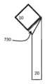
도19a-19c는 도19a에 가장 잘 보이는 것처럼, 제2 도파관(20)의 평행면 중 하나에 인접한 제1 도파관(10)을 배치함으로써 도파관을 결합하기 위한 본 발명의 일 실시예에 따르는 상이한 구성을 도시한다. 광은 도1a에 참고로 전술된 바와 같이, 우측에서 좌측으로 제1 도파관(10) 안에서 전파되고, 중간 굴절 층(99)(이하 논의되는)을 통해 제2 도파관(20)의 면에 이미지를 커플링-인하도록 편향된 이미지를 편향시키도록 여기에 배향된 도파관(10)의 내부 파셋(도19c의 상면도에서 볼 수 있는)을 마주한다. 결합은 제2 도파관920) 내에서, 바람직하게는 TIR(도19b의 실선 화살표)을 통해 광속이 지속적으로 반사되도록 선택된 각도에 있다. 공액 방향(도19b의 점선 화살표)으로 제2 도파관(20)에 커플링 인되는 공액 빔은 제2 도파관(20)의 인접 단부로 전파하고 외부 산란에 의해 손실된다.Figures 19a-19c illustrate a different configuration according to one embodiment of the present invention for coupling waveguides by placing a
이 구현예에서, 제1 도파관(10)으로부터 결합된 이미지로 제2 도파관(20)을 채우는 것은 바람직하게는 제1 도파관(10)의 폭을 충분하게 선택함으로써 달성되어, 이미지의 가장 얕은 각도 영역에 대한 도파관(10)의 원거리 단부(도19b의 도시된 바와 같은 상단)에서 나타나는 광속(101)이 제1 도파관(10)의 다른 단부(102)를 지나치지 않을 것이다.In this embodiment, filling the
도19a-19c의 구성을 구현하기 위해, 다수의 조건이 충족되어야 한다. 먼저, 제1 도파관(10)을 따르는 전파를 지원하기 위해, 도파관(10) 안으로 도입된 광속은 굴절 층(99)와의 인터페이스에 의해 반사되어야 한다. 도파관(10)의 내부 파셋에 의한 반사 후에, 광속은 제2 도파관(20) 안으로 굴절 층(99)을 통해 커플링-아웃되어야 하지만, 도파관(20)의 대향하는 외부 면으로부터 벗어나서는 안 된다. 도20은 상기 조건을 충족시키도록 이 구성을 구현하기 위한 접근법을 구 좌표계로 도시한다.In order to implement the configuration of Figures 19a-19c, a number of conditions must be met. First, in order to support propagation along the
따라서, 도20에서, 이미지(106LU, 106RU, 106LD, 106RD)는 도1a의 a1, a2,a3 및ㅁ4와 동일하다. 도파관과 공기 사이의 임계 각도는 각각 도3의 61 및 63과 동일한 원(107 및 108)로 표시된다. 원(109)은 도19b 및 19c의 도파관(10)과 중간 굴절 층(99) 사이의 임계 각도를 나타낸다. 도파관과 굴절 층(99)의 굴절률의 비가 공기 보자 작기 때문에, TIR 원은 공기 경계에서보다 크다. 제1 도파관(10)을 따라 전파하는 4개의 공액 이미지는 모두 두 원(107 및 109) 외부에 존재하여, 이미지는 도파관을 따라 TIR을 통해 전파한다. 106LU가 도파관(10)의 내부 파셋을 마주하면, 110LU 상에 결합되고 106RU는 110RU에 결합된다. 빔(110LU 및 110RU)은 임계 각도(109 내에 존재하지만 임계 각도(107) 외부에 존재한다. 결과적으로, 그것들은 층(99)을 통해 효과적으로 도파관(10)에서 커플링-아웃되고 도파관(20)에 커플링-인되지만, 도파관(20)의 외부 면으로부터 공기로 커플링-아웃하지는 않을 것이다.Accordingly, in Fig. 20, the images 106LU, 106RU, 106LD, and 106RD are the same as a1, a2, a3 and ㅁ4 in Fig. 1A. Critical angles between the waveguide and air are indicated by
110LU 및 110RU가 제2 도파관 내에서 반사되면, 그들의 대응하는 공액 이미지(110LD 및 110RD)를 각각 생성한다. 이 반사는 도1a의 b2와 동일하다.When 110LU and 110RU are reflected within the second waveguide, they produce their corresponding conjugate images 110LD and 110RD, respectively. This reflection is the same as b2 in Fig. 1A.
전술된 바와 같이, 이 구현예에서, 110RU 및 110RD는 도19b의 점선 화살표에 의해 설명된 바와 같이 산란된다. 이미지(110LD)은 제2 도파관(20)의 내부 파셋에 의해 눈에 커플 아웃된다(도1a의 45에서 도시된 바와 같이).As described above, in this implementation, 110RU and 110RD are scattered as illustrated by the dotted arrows in FIG. 19B. Image 110LD is coupled out to the eye by the inner facet of second waveguide 20 (as shown at 45 in FIG. 1A).
이 실시예의 다양한 구현예가 도21a 및 21b에 도시되어 있다. 도21a에서, 빔(110RU, 110RD)(점선 화살표로 도시된)은 반사되어 중첩되고 보강된다(110LU, 110LD)(실선 화살표). 이 조합은 도21a에 도시된 바와 같이 제2 도파관(20)의 단부에서 수직으로 반사기(112)를 도입함으로써 달성된다. 이 반사기는 이미지(110RU, 110RD)의 일부분이 역으로 반사되고 대향 방향으로 제1 도파관(10)에 다시 들어가도록 한다. 내부 파셋에 의해 반사된 후에 이 빔들을 포함하도록 제1 도파관(10)의 두 개의 대향 외부 파셋(114R, 114L)상에 반사성 코팅을 제공하는 것이 바람직할 수 있다.Various implementations of this embodiment are shown in FIGS. 21A and 21B. In Fig. 21A, beams 110RU and 110RD (shown as dotted arrows) are reflected, superimposed and reinforced (110LU and 110LD) (solid arrows). This combination is achieved by introducing a
도21b는 도21a의 구성과 동일한 기능을 유지하면서 제1 도파관 반사기(114R)과 제2 도파관 반사기(112)를 단일 반사기(116)로서 결합하는 구성을 도시한다.FIG. 21B shows a configuration in which the
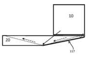
도21c에서, 도파관(10)은 또한 중간 유전체 또는 공기-간극에 의해 이격된 도파관(20)에 인접한다. 도파관(10)으로부터 커플-아웃된 광(실선 화살표)은 도13a 및 13b를 참고로 전술된 과정과 유사한 과정으로 도파관(20) 상의 백 미러(117)에 의해 반사된다. 미러(117)의 각도는 도파관(20)의 필요한 유도된 광 각(점선)에 도파관(10)으로부터 투과된 광을 정합(match)시키도록 선택된다. 일부 경우, 미러(117)는 사용된 도파관(10) 및 이미지 전파 각도에 의해 생성된 커플링-아웃 각도에 따르는 도파관(10)의 에지를 넘어 연장된다.In Fig. 21c,
내부 파셋(또는 회절 광학 소자)에 의한 이미지 커플링-아웃의 상이한 형상은 예를 들어 도2a 및 2b를 참고로 전술된 다양한 형상 및 적절한 코팅과 같은 도19a-21c의 구현예에 적용될 수 있다.Different shapes of image coupling-out by internal facets (or diffractive optical elements) may be applied to the implementation of FIGS. 19a-21c, such as, for example, the various shapes and appropriate coatings described above with reference to FIGS. 2a and 2b.
도19a-21b의 구현예는 도20을 참고로 설명된 기하학적 형상 요건에 의해 사용가능한 관측 시야에 어느 정도 한정된다. 그럼에도 불구하고, 적용 범위에 있어서, 이 옵션은 디자인의 단순성 및 제조의 용이성으로 인해 특히 유리할 수 있다.The implementation of FIGS. 19A-21B is limited to some extent in the usable field of view by the geometry requirements described with reference to FIG. 20 . Nevertheless, in terms of application, this option can be particularly advantageous due to its simplicity of design and ease of manufacture.
제1 도파관(10)과 제2 도파관0) 사이의 결합 구현예의 또 다른 세트가 도22a 및 도22e에 도시되어 있다. 이 구현예에서, 도22b에 도시된 바와 같이, 2D 도파관(10)은 제2 도파관(20)에 대해 경사져 있어서 도파관(10)으로부터 커플 아웃된 이미지 중 오직 하나가 포함되고 도파관(20) 내에 안내된다. 제1 도파관(10)은 중간 투명 쐐기(730)의 사용에 의해 1D 도파관(20)에 대해 필요한 경사로 장착될 수 있다. 이 경사는 도파관(10)으로부터 하나의 이미지를 결합하고(도19b의 실선 화살표와 유사한, 실선 화살표) 도파관(10)으로부터 다른 이미지를 결합하지 않도록(도19b의 점선 화살표와 유사한, 점선 화살표) 선택된다. 결합되지 않은 이미지는 외부 흡수체, 예를 들어 736에 의해 흡수되거나 관찰자가 볼 수 없는 방향을 향하게 된다. 선택적으로, 736은 광을 대향 방향으로 도파관(10) 안으로 다시 반사시키고, 도파관(20)에 커플링-인하는데, 도21a-21b의 점선 화살표와 동일하다. 이 옵션에 따르면, 도22b에 도시된 바와 같이, 반사 코팅은 2D 도파관의 외부 파셋 중 적어도 하나 상에 제공된다. 설명의 명확성을 위해, 도파관의 내부 파셋은 이 도면에서 생략되었다.Another set of coupling implementations between the
도파관(20)에 대한 도파관(10)의 경사는 도파관 및 그 사이에서 전파하는 이미지의 필요한 각도에 따라 선택될 수 있으며, 도22c에 도시된 바와 같이, 제2 도파관(20)의 경사진 결합 표면에 대해 경사를 감소시키거나 도22d에 도시된 바와 같이 각도를 증가시키기 위해, 투명한 쐐기 결합 프리즘(730)을 이용할 수 있다. 도22e에 도시된 바와 같이 특히 바람직한 구현예에서, 제2 도파관(20)에 대한 제1 도파관(10)의 필요한 경사는 제2 도파관 결합 표면의 각도와 일치하므로, 어떤 중간 결합 프리즘도 필요하지 않다. 이 옵션을 구현하기 위해, 제2 도파관(20) 안으로 결합된 이미지의 출력 각도는 도파관(20) 내의 필요한 전파 각도와 일치하여야 하며, 도파관(10)의 경사진 단부 표면(734) 및 차원에 의해 구성된 쐐기의 범위는 이미지 및 그 공액으로 제2 도파관을 채우는 것이 도6-12를 참고로 전술된 것과 유사한 방식으로 달성되게 할 수 있는 것이다.The inclination of the
각각의 경우, 인터페이스 불연속성은 도파관 속성이 손상되지 않도록 제1 도파관의 출력 면에 필요하다. 도22a-22e에 도시된 구현예에서, 도파관(10)과 도파관(20) 사이에 광학적 불연속성을 제공하는 중간 매체는 공기이지만, 임의의 다른 굴절 물질 또는 코팅도 사용될 수 있다. 옵션은 전술된 내부의 부분 반사 파셋의 대안으로서, 출력 결합을 수행할 수 있는 회절 격자를 포함한다.In each case, an interface discontinuity is required at the output side of the first waveguide so that the waveguide properties are not compromised. In the implementation shown in Figures 22a-22e, the intermediate medium providing the optical discontinuity between
따라서 도22a-22e는 제1 도파관(10)이 제3의 평면 면(22a, 22b) 쌍 사이에서 연장되고 제3의 평면 면(22a, 22b) 쌍에 대해 비스듬하게 경사진 제2 광학 도파관(20)의 단부 표면에 광학적으로 결합되는 도파관(10)의 경사를 도시한다. 이 유형의 경사는 예를 들어 도26-29를 참고로 이하 설명되는 다양한 상이한 유형의 내부 파셋 경사와 같은, 여기에 제시된 모든 다른 다양한 구성과 결합될 수 있다.22a-22e thus shows a second optical waveguide in which the
도23 및 24를 살펴보면, 이들은 전술된 도1a-1b의 것과 본질적으로 유사한 구현예에 관한 것이지만, 다수의 가변적인 특성을 도시한다. 따라서, 도23은 중간 굴절 층(120)이 도파관(10 및 20) 사이에 개재된 구현예를 도시한다. 이 층은 바람직하게는 얇아야하며, 다양한 물질 또는 다층 코팅으로 제조될 수 있다. 층(120)의 존재는 도3의 임계 각 원(61)을 확대하는 기능을 하며, 도24의 각도 공간도의 임계 각 원(121)으로서 도시된다. 굴절률의 적합한 선택에 의해, 이 임계 원의 크기를 선택하는 것이 가능하여, 광학 디자인에서 추가적인 자유도를 제공하고, 일부 경우 공기 간극으로 달성될 수 있는 것보다 큰 FOV를 갖는 구현을 용이하게 한다.Referring to Figures 23 and 24, they relate to implementations that are essentially similar to those of Figures 1A-1B described above, but show a number of variable characteristics. Accordingly, FIG. 23 shows an implementation in which an intermediate
독립적인 양태에서, 도24는 또한 a3 및 a4가 a1 및 a2에 대해 도파관(10)의 파셋의 각도의 동일 측면상에 존재하는 구현을 묘사한다. 이것은 도2a의 C1의 시나리오와 동일하다.In an independent aspect, Figure 24 also depicts an implementation in which a3 and a4 are on the same side of the angle of the facets of
또 다른 독립적인 양태에 따르면, 도24는 도파관(10, 20)이 상이한 굴절률을 갖는 물질로 구성되는 구성을 도시한다. 상이한 결과적인 특성을 나타내기 위해, 제2 도파관의 기하적인 형상 특정은 도24의 좌측에 별도로 도시되어 있으며, 이미지의 각도 크기와 임계 각 원이 두 그림에서 상이하다.According to another independent aspect, Fig. 24 shows a configuration in which the
상기 변형 모두는 당업자에게 명백한 바와 같이, 시스템 디자인의 추가적인 자유도를 제공하도록 여기에 기재된 실시예와 조합하여 사용될 수 있다.All of the above variations can be used in combination with the embodiments described herein to provide additional degrees of freedom in system design, as will be apparent to those skilled in the art.
본 발명의 다양한 실시예에서, 부품, 특히 두 도파관의 상대적인 배치에서 정밀한 정렬 및 구조적 안정성은 높은 이미지 품질을 보장하는데 중요할 수 있다. 도25a-25d는 본 발명에 따르는 디바이스의 조립체에 대한 다수의 상이한 옵션으로, 다양한 추가적인 장점을 제공한다.In various embodiments of the present invention, precise alignment and structural stability in the components, particularly in the relative placement of the two waveguides, can be important to ensure high image quality. 25a-25d show a number of different options for assembly of a device according to the present invention, providing various additional advantages.
도25a는 이미지 품질을 보존하기 위해 외부 면 표면 수직성을 유지하면서 도파관(20)의 상단에 도파관(10)을 구현하기 위한 제1 옵션을 도시한다. 이 옵션에 따르면, 연속적인 외부 커버(132)가 도파관(10 및 20)에 제공된다. 하나의 바람직한 옵션에 따르면, 외부 커버(132)는 도파관의 물질과 광학적으로 일치하여, 실제 도파관이 커버(132)의 외부 면에 의해 실제로 규정되는 반면, 내부 파셋은 커버의 내부를 향하는 인터페이스 사이에만 제공된다. 이 경우, 외부 커버(132)는 광학 누출(136)을 최소화하기 위해 가능한 한 얇아야 한다. 도파관(10 및 20) 사이에 도시된 간극은 임계 각도 관리를 위한 공기 간극 또는 굴절 간극일 수 있다.Figure 25a shows a first option for implementing the
도25b는 도25a의 것과 유사하지만, 도파관(10)의 상단 및 하단을 따라 광학 커버(142)를 추가로 갖는 구현예를 도시한다. 이러한 커버의 사용은 이 면을 따라 높은 광학 품질 획득을 용이하게 한다.FIG. 25B shows an implementation similar to that of FIG. 25A, but with the addition of
도25c는 도파관 사이의 부착이 임의의 간극 또는 편차에도 불구하고 도파관(20)에 대한 입구의 완전한 커버리지(채움)를 보장하기 위해 도파관보다 약간 넓은 구현예를 도시한다. 이 경우, 중간 굴절 물질 층149)은 바람직하게는 도파관(10)의 전체 하단 표면을 덮는다.Figure 25c shows an implementation where the attachments between the waveguides are slightly wider than the waveguides to ensure full coverage (filling) of the entrance to the
도25d는 두 도파관 사이의 공기 간극으로 구현된, 도22a-22e와 유사한 기하학적 형상을 갖는 구현예에 관한 것이다. 도파관의 상대적인 위치를 고정하고 도파관의 내부 반사의 최소 섭동(perturbation)으로 그들 사이의 공기-간극을 밀봉하기 위해, 반사 코팅(1149)이 바람직하게는 적어도 연결(joinning)이 수행될 때의 영역의 도파관의 외부 면상에 도포된다. 그 다음에 연결 기구(joining attachment, 1150)는 기계적으로 도파관을 상호연결하기 위해 이들 코팅의 각각에 부착되며, 바람직하게는 밀봉을 생성한다. 코팅은 간극에 가깝게 국한될 수 있거나, 2D 도파관의 전체 측방향 면을 덮는다.Fig. 25d relates to an embodiment having a similar geometry to Figs. 22a-22e, implemented as an air gap between two waveguides. In order to fix the relative positions of the waveguides and seal the air-gap between them with minimal perturbation of the internal reflections of the waveguides, the
코팅(1149)은 금속성 반사 코팅일 수 있거나, 산란으로부터 가파른 광선 또는 임의의 원하지 않는 이미지가 투과되는 동안 이미지 광의 그레이징 각도(grazing angle)가 반사되도록 유전체 코팅이 선택될 수 있다.
도26을 살펴보면, 이 구현예에서, 도파관(10)의 연장 방향은 제2 도파관(20) 내의 파셋의 연장 방향에 대해 기울어진자(비-평행). 다시 말해서, 제2 도파관(20)의 부분 반사 표면(파셋(45))은 한 세트의 평행선(150)에서 면(22a)과 교차하고, 제2 도파관(20)의 커플링-인 단부 표면은 에지(151)에서 면(22a)과 만나며, 이 에지는 이 평행선 세트에 비-평행이다. 이 경사는 이미지의 아웃-커플링 각도을 변경하고 특정 응용의 인체공학적 디자인에 대한 요건을 충족시키기 위해 사용될 수 있다. 이 각도 제한은 임계 각도를 초과하지 않도록 하는 제한, 또는 정상 이미지를 중첩시키는 고스트 이미지(도24의 122와 같은 파셋 라인을 교차하지 않는 이미지 직사각형)를 갖지 않도록 하는 요건을 포함한다.Referring to Figure 26, in this embodiment, the direction of extension of the
도26의 구현예에서, 제2 도파관(10) 내의 파셋의 각도는 제2 도파관(20)에 공급된 링크- 아웃된 이미지가 제2 도파관 파셋에 수직으로 전파되도록 선택된다.In the embodiment of Fig. 26, the angle of the facets in the
도파관(20)에 대한 도파관(10)의 경사는 선택적으로 파셋 구조(도2a 및 2b의 옵션), 결합 방법(도19a-23), 필요한 이미지 FOV, 및/또는 공기 및 도파관 사이의 임계 각(도24)에 따라 여기에 도시된 것과 반대의 의미일 수 있다.The inclination of the
도27은 제1 도파관(10)의 부분 반사 표면(155)이 두 면(12a 및 14a)에 비스듬한 각도로 존재하는 본 발명의 또 다른 변형 예를 도시한다(점선은 두 외부 면에 수직인 평면과, 오직 한 면에 대해 기울어진 다른 평면을 보여줌으로써, 파셋의 경사를 용이하게 시각화하기 위한 것이다). 각도 공간에서의 이 구현예의 설명은 도28에 도시되어 있다. 도파관(10)의 초기 이미지는 "가로로 긴"(광(wide)) 종횡비를 갖는 a1-a4로서 표시된다. 이미지들은 최종 수평 이미지를 획득하기 위해 비뚤어진 각도에 있는 이미지(a1)처럼 도파관 안으로 주입된다. 2D 경사 내부 파셋(155)의 평면은 157로 표시된다. 이 파셋은 도파관(10)으로부터 도파관(20) 안으로 아웃-커플된 b1에 a1을 커플링-인한다. 다른 한편으로, a2는 임계 각도 여분에 존재하지 않고 따라서 도파관(20)에 결합되지 않고, 그 대신에 손실되는 b2에 결합된다. 이미지(b1)는 자신의 공액 이미지(b3)를 도파관(20) 내에 생성하고 결국 이미지 c처럼 눈에 커플링-아웃된다(전술된 바와 같이). 이 구조에서, 도파관(10 및 20) 사이의 정렬의 정밀도에 대한 요구는 완화된다.Figure 27 shows another variant of the present invention in which the partially
도29a 및 29b의 각도 공간에 표시된 도27의 또 다른 변형 예에 따르면, 파셋(40)의 배향은 제1 도파관(10) 내에서 전파하는 4개의 이미지 중 오직 하나의 상당한 부분을 선택적으로 반사하도록, 110으로 표시된 2D 틸트 및 적합한 코팅으로 선택될 수 있다. 따라서, 도29a에 도시된 형상에서, 이미지(a2)는 선택적으로, 도파관(20) 안에서의 전파 및 연장을 위해 커플 아웃된 b1에, 커플링-인된다. 나머지 이미지(a1, a3 및 a4)는 충분히 작은 각도에 존재하여, 코팅의 적합한 선택에 의해, 파셋(40)에서의 이 이미지들의 반사를 실질적으로 제거하는 것이 가능하다. 이미지(a2 보다 파셋 평면에 더 가까운 a1, a3)의 각도 차이는 도29b의 3D 표현에서 가장 잘 보인다. 따라서, 특히 바람직한 일 예에서, 표면에 대한 법선에 대해 55°내지 85°사이로 입사하는 광선에 대해 실질적으로 투과하게 하고(즉, 관련 파장 범위에서 입사 방사선의 5% 미만의 반사를 생성하는), 법선에 대해 45°미만의 경사로 입사라는 광선에 대해 부분적으로 반사하도록(입사 방사선 강도의 적어도 10%에서, 상당히 많은, 전형적으로 "실질적으로 투과한" 각도 범위보다 적어도 두 배의 반사 강도로, 전형적으로 반사하는), 파셋(40)이 코팅된다. 이미지의 각도 방향의 입사 각도 및 파셋 경사 각도는 3개 이미지(여기서는 a1, a3, 및 a4)에 대한 전체 분포(spread) 각도가 실질적으로 투과한 각도 범위 내에 있지만, 한 이미지(여기서는 a2)에 대한 이미지 각도는 부분 반사 범위 내에 있도록 선택될 수 있다. 이것은 오직 한 이미지의 선택적인 커플링-아웃을 야기하여, 시스템 디자인의 다양한 양태를 단순화합니다. 커플-아웃된 이미지는 원래 생성된 것과 동일할 필요가 없으며, 대신에 원래 생성된 이미지의 역전된 공액 이미지일 수 있다는 점에 유의하여야 한다. 필요하다면, 원래 이미지 생성 소자는 주입을 위한 역전된 공액 이미지를 생성하여 우측 이미지가 도파관으로부터 아웃-커플되도록 한다.According to another variant of FIG. 27 shown in the angular space of FIGS. 29a and 29b, the orientation of the
균일성 향상(Uniformity Enhancement)Uniformity Enhancement
최종 연장된 개구 조명의 비-균일성은 때때로 원래의 투사된 이미지 개구의 비-균일 광 또는 이 개구의 최적화되지 않은 트리밍으로부터 야기될 수 있다. 본 발명의 또 다른 양태에 따르면, 이러한 비-균일성은 도파관의 다중-경로 구성을 구현함으로써 평탄화(smoothed-out)될 수 있다.Non-uniformity of the final extended aperture illumination can sometimes result from non-uniform light in the original projected image aperture or non-optimal trimming of this aperture. According to another aspect of the present invention, this non-uniformity can be smoothed out by implementing a multi-pass configuration of the waveguide.
도30을 구체적으로 살펴보면, 이것은 인접한 평행 도파관(172)이 나란히 놓인 도파관(170)(도파관(10 또는 20)의 측면도일 수 있음)을 도시한다. 중간 면(도파관(170 및 172) 사이의) 및 외부 면(도시된 바와 같이 상단 및 하단)은 평행하다. 중간 인터페이스에서의 부분 반사는 도파관 사이의 코팅 또는 굴절률 불연속성을 기반으로 한다. 도파관(170) 내에서 전파하는 반사된 개구(174)는 176(점선으로 표시된)처럼 도파관(172) 안에 결합된다. 개구의 이미지는 또한 도파관(170)에 커플링-인되고, 그리고 내부 파셋(40 또는 45)에 의해 "원래" 개구(179)와 함께 출력 개구(178)에 커플링-아웃된다. 출력 개구(178 및 179)는 평행하지만, 위치가 오프셋되어 있어(offset), 개구를 가로지르는 비-균일성을 평균화한다.Turning specifically to Fig. 30, it shows a waveguide 170 (which may be a side view of
감지된 비-균일성의 다른 원인은 도31a에 도시된 바와 같이 상이한 관측 시야의 내부 파셋의 각도 중첩에 관한 것이다. 여기에 도시된 도파관(10 또는 20)의 영역에서, 도파관은 내부 파셋을 포함한다(40 또는 45와 동일한, 두 파셋(2515 및 2517)이 표시되어 있다). 아웃-커플된 광의 대부분은 단일 내부 파셋으로부터 반사된다. 그러나, 파셋의 에지에는, 축과 다른 방향(off-axis)의 각도에 비균일성이 있다. 좌측을 가리키는 FOV의 영역(실선 화살표로 표시된)에 대해, 2520으로 표시된 영역은, 이 각도에서 감지된 어두운 스트립을 초래하는, 파셋(2515) 및 파셋(2517)에 의해 반사된 광 사이의 효과적인 간극이 존재하기 때문에, 어떤 광도 반사하지 않을 것이다. 다른 한편으로, 우측에 커플-아웃된 광(점선 화살표로 표시된)은 파셋(2515 및 2517)로부터 반사된 광의 중첩이 존재하는 영역(2525)을 가져서 거의 2배의 광 량을 반사할 것이다. 따라서, 도31a의 비-균일성은 FOV 및 눈 위치의 상이한 영역에서 연장된 개구를 가로질러 대략 200% 내지 0%의 중간 이미지 강도에서 변할 것이다.Another source of perceived non-uniformity relates to the angular overlap of the inner facets of the different viewing fields, as shown in Fig. 31a. In the region of
본 발명의 또 다른 양태에 따르면, 도31b에 도시된 바와 같이, 상당한 중첩이 파셋 사이에 도입된다. 이 경우, 인접한 파셋 사이의 간격은 절반이 되어, 대부분의 눈 위치에서 FOV의 대부분이 두 파셋으로부터의 중첩된 반사를 통해 이미지로부터 조명을 수신하게 된다. 이미지의 각도 맨 끝(extremities) 및 파셋의 맨 끝 근처에는, 3개의 인접한 파셋에 의해 제공되는 빔(2545) 및 오직 하나의 파셋으로부터 유래되는 빔(2540)에 의해 도시되는 바와 같이, 이미지의 특정 영역의 원인이 되는 중첩 파셋 수의 변화는 여전히 존재할 것이다. 그럼에도 불구하고, 비-균일성은 크게 감소하며, 일반적으로 대략 ±50%에 해당한다. 게다가, 개구를 가로질러 더욱 가깝게 이격된 위치에서 발생하는 변형은 관찰자의 동공에서 평균화되어 변형이 눈에 띄지 않게 되는 경향이 있다.According to another aspect of the present invention, significant overlap is introduced between the facets, as shown in FIG. 31B. In this case, the spacing between adjacent facets is halved, so that at most eye positions, most of the FOV receives illumination from the image through overlapping reflections from both facets. At the angular extremities of the image and near the extremities of the facets, certain features of the image are shown by
비-균일성을 감소시키기 위한 또 다른 개선은 도31c에 도시된 바와 같이, 중첩하는 내부 파셋에 의해 생성되는 "다중경로" 이미지의 도입으로부터 초래될 수 있다. 도파관(10)내에서 전파하는 광(실선 화살표로 표시되고 'a'로 표기된)은 커플 아웃되지만('b'로 표기된), b로부터의 광의 일부는 'b'로서 커플 아웃되기 전에 'a'(점선 화살표로 표시된)에 다시 결합된다. 'a'와 'b' 사이의 앞-뒤(back-and -forth) 결합은 광 평행도(parallelism)를 유지하면서 개구를 가로질러 강도를 평균화함으로써, 광 균일성을 추가로 향상시킨다.Another improvement to reduce non-uniformity can result from the introduction of "multipath" images created by overlapping inner facets, as shown in Fig. 31c. Light propagating in the waveguide 10 (indicated by solid arrows and labeled 'a') couples out (labeled 'b'), but some of the light from b is 'b' before being coupled out as 'a'. (indicated by the dotted arrow). The back-and-forth coupling between 'a' and 'b' further enhances light uniformity by averaging the intensity across the aperture while maintaining light parallelism.
본 발명의 특정 구현예에 따르는 교차-결합의 다른 방법은 도32a 및 32b에 도시되어 있다. 도32a에서, 내부 파셋(2670)(40과 동일한)은 내부 파셋에서 우측에서 좌측으로 TIR을 통해 전파하는 이미지 조명의 일부를 상부 외부 면(2675)상까지 위쪽으로 반사하도록 "역" 방향으로 있다. 이 면(2675)은 코팅되어 전체 반사기가 되도록 하며, 따라서 광을 도파관(20) 안으로 아래쪽으로(광선(2672)) 반사시킨다.Another method of cross-linking according to certain embodiments of the present invention is illustrated in FIGS. 32A and 32B. In FIG. 32A, inner facet 2670 (equivalent to 40) is oriented "reversely" so as to reflect some of the image illumination propagating through TIR from right to left in the inner facet upward onto
상부 외부 면(2675)으로부터 반사된 광의 일부는 내부 파셋에 의해 다시 반사되고(점선 화살표로 도시된) 광선(2680)처럼 아래쪽으로 다른 내부 파셋에 의해 반사될 때까지 도파관(10)을 따라 후방으로 전파된다. 광속(2672 및 2680)은 평행하고 서로로부터 떨어져 있기 때문에, 이미지 강도의 비-균일성의 평탄화 및 교차 결합을 달성하는 것이 명확하다.Some of the light reflected from the upper
도32b에서, 내부 파셋은 광을 아래쪽으로 결합하도록 도시되어 있으며(위쪽 결합도 이 실시예에 포함되어 있다), 하단 외부 면(2705)은 부분 반사기로서 구현되고 상단 외부 면(2710)은 전체(예를 들어, 금속화된) 반사기로서 구현된다. 이 구성의 결과로, 내부 파셋(40)에 의해 아래쪽으로 반사되고 통상적으로 커플-아웃되는 광의 일부는 그 대신에 제1 도파관(10) 안으로 다시-반사될 것이다. 상향 광선(점선으로 표시된)은 그 다음에 다중 경로 안으로 분할되는데, 일부는 내부 파셋을 통과하고 상부 면(2710)으로부터 반사하고, 일부는 후속 내부 파셋에서 위쪽으로 반사되도록 들어오는 광선 경로를 따라 역방향으로 다시 반사된다. 상부 면(2710)으로부터 반사된 광선은 마찬가지로 커플링 아웃을 위해 내부 파셋을 곧게 통과할 수 있거나, 상이한 위치에서 커플 아웃되도록 내부 파셋상에서 또 다른 쌍의 반사를 겪을 수 있다. 이미지 사이의 다중-경로 혼합 및 교차-결합은 비-균일성을 감소시키는 역할을 추가로 한다.In FIG. 32B, the inner facets are shown to couple light downward (upper coupling is also included in this embodiment), with the lower
커플링-아웃 면에 대해 높은 각도에서 발생하는 전술된 다중 내부 반사는 또한 도파관(10)의 전방 및 후방 면에 충돌할 것이라는 것을 알 수 있을 것이다. 빔의 각도에 따라, 반사 코팅으로 도파관(10)의 전방 및 후방 면을 추가로 코팅하는 것이 바람직할 수 있다.It will be appreciated that the aforementioned multiple internal reflections occurring at high angles to the coupling-out face will also impinge on the front and back faces of the
도33a-33c를 살펴보면, 도3, 24, 28 및 29를 참고로 전술된 체계에서, 내부 파셋에서의 선택 부분 반사는 파셋에 대해 상대적으로 높은 경사에 있는 입사 이미지(a1 및 a2)에 대해 발생하지만, 낮은 경사 각 이미지(a3 및 a4)가 투과되도록 도록 디자인된다. 전술된 바와 같이, 이 선택적인 특성을 달성하기에 적합한 파셋 코팅은 당업계에 공지되어 있고, 양수인의 종래 미국 특허 제7391573호 및 제7457040호에 설명되어 있는 것을 알 수 있다.Referring to Figs. 33a-33c, in the scheme described above with reference to Figs. 3, 24, 28 and 29, select partial reflections at the inner facet occur for incident images a1 and a2 at a relatively high inclination to the facet. However, it is designed so that the low tilt angle images a3 and a4 are transmitted. As noted above, facet coatings suitable for achieving this selective property are known in the art, and it will be appreciated that they are described in the assignee's prior US Pat. Nos. 7391573 and 7457040.
이 접근법에 대한 대안으로서, 도33a-33c는 낮은-경사 이미지는 커플 아웃된 이미지이고, 높은 경사 이미지는 파셋을 통해 투과되는 구현예를 도시한다. 따라서, 도33b의 각도 도면에서, b1 및 b2를 제공하도록 커플 아웃된 이미지는 a3 및 a4이고, 이미지 a1 및 a2는 최소 반사로 내부 파셋(40)을 통과한다. 이 광선 형상은 도33a에 도시되어 있고, 도2a의 광선(c2)의 커플링 아웃과 기하학적으로 동일하다.As an alternative to this approach, Figures 33a-33c show an implementation where the low-tilt image is a coupled out image and the high-tilt image is transmitted through the facet. Thus, in the angular view of Fig. 33b, the images coupled out to give b1 and b2 are a3 and a4, and images a1 and a2 pass through
도33c는 이 선택성을 달성하는데 사용되는 내부 파셋의 각도 반사율의 예를 도시한다. 이 그래프에서, 파셋에 대한 법선에 대한 각도는 x-축을 따라 디스플레이되고, 각각의 편광의 반사율은 y-축에 디스플레이된다. 실선 사각형은 a3 또는 a4의 각도 범위를 나타낸다. S-편광은 부분적으로 반사되지만, P-편광은 대부분 투과되는 것이 분명하다(상기 실시예에에 설명된 바와 같이). 점선 사각형은 공액 이미지(a1 및 a2)를 나타낸다. 두 편광에서의 반사는 최소한이어서 도파관(10) 밖으로 반사되지 않을 것이다.Figure 33c shows an example of the angular reflectivity of the inner facets used to achieve this selectivity. In this graph, the angle to the normal to the facet is displayed along the x-axis, and the reflectance of each polarization is displayed along the y-axis. The solid line rectangle represents the angular range of a3 or a4. It is clear that S-polarized light is partially reflected, while P-polarized light is mostly transmitted (as described in the previous example). Dotted squares represent conjugated images (a1 and a2). Reflection in both polarizations is minimal and will not reflect out of the
이 반사율 프로필을 달성하기 위해 필요한 코팅은 전술된 US7391573 및 US7457040에서와 같이, 1D 도파관의 맥락에서 개시된 코팅을 사용하여 구현될 수 있다.The coatings necessary to achieve this reflectance profile can be implemented using the coatings disclosed in the context of 1D waveguides, such as in the aforementioned US7391573 and US7457040.
편광 체계polarization scheme
파셋 코팅의 반사 속성은 편광 의존적이다. 이 강력한 의존성은 편광이 일정하게 유지되지 않는 경우 관찰자에게 투사된 이미지의 비-균일 강도 출력을 생성할 수 있다. 따라서, 1D 도파관을 써서 작업할 때 통상적인 관행은 도파관 표면에 대해 직교하는 배향으로 단일 편광(바람직하게는 S)을 사용하여 그들을 조명하는 것이다. 이 분광 배향은 그 다음에 광이 1D 도파관을 따라 전파할 때 변하지 않는다.The reflective properties of facet coatings are polarization dependent. This strong dependence can produce a non-uniform intensity output of the projected image to the observer if the polarization is not kept constant. Thus, a common practice when working with 1D waveguides is to illuminate them with a single polarization (preferably S) in an orientation orthogonal to the waveguide surface. This spectral orientation then does not change as the light propagates along the 1D waveguide.
본 발명의 일 양태의 교시에 따르는 2D 도파관(10)의 맥락에서, 입력 이미지에 대한 단일 편광의 사용은 광이 다양한 각도에서 면에 충돌하여 이 반사들을 통해 편광 배향의 수정을 야기하기 때문에, 최적 해법을 제공하지 않는다. 결과적으로, 단일 편광이 도파관상에 주입되는 경우, 그 배향은 도파관을 따라 변경되고 이미지 균일성은 손상될 것이다.In the context of a
대신에, 본 발명의 특정한 특히 바람직한 구현예에 따르면, 제1 도파관(10) 안으로 도입된 이미지는 2D 도파관 안으로 무편광(또는 후술되는 바와 같이, 의사(pseudo)-무편광)처럼 커플 인된다. 무편광 입력을 사용함으로써, 편광의 회전은 이미지 균일성에 어떤 영향도 미치지 않는다. 또한, 내부 파셋(40)으로부터의 아웃-커플링 반사가 크게 편광된 출력을 생성할지라도, 부분적으로 편광되고 투과된 이미지는 도파관 면에서 후속 반사에 의해 연속적으로 변환된(scrambled) 자신의 편광을 갖고, 따라서 후속 내부 파셋에서 커플 아웃된 이미지의 균일성에 기여한다.Instead, according to certain particularly preferred embodiments of the present invention, the image introduced into the
광학 이미지는 스캔 레이저, LCD, LCOS, DLP, OLED 또는 광을 방출하는 다른 디바이스에 의해 생성될 수 있다. 투사된 광이 편광화될 경우, 또는 편광화가 편광된 빔 스플리터에 의해 도입되는 경우, 광은 바람직하게는 제1 도파관(10)의 개구에 들어가기 전에 탈편광자(depolarizer)를 통해 투과된다. 탈편광자는 광의 상이한 스펙트럼 성부의 편광 변화에 기반하는 수동 탈편광자("Lyot" 탈편광자, "Cornu" 탈편광자, 또는 "웨지(Wedge)" 탈편광자)일 수 있다. 예를 들어, 적색, 녹색 또는 청색 LED의 스펙트럼 폭은 대략 50나노미터이며, 1mm 두께의 크리스털 석영은 우수한 탈편광을 달성할 수 있다. 이러한 탈편광자는 이미지 투사 장치의 마지막 편광 소자 뒤에 있는 이미지 전파 경로를 따라 임의의 광학 인터페이스에 도입될 수 있다. 예를 들어, 도16의 편광된 빔 스플리터(513) 바로 아래에, 또는 도파관 제조 도중에 결합되는 임의의 소자 사이의 중간 인터페이스에 도입될 수 있다.Optical images can be created by scanning lasers, LCDs, LCOSs, DLPs, OLEDs or other devices that emit light. If the projected light is polarized, or if polarization is introduced by a polarized beam splitter, the light is preferably transmitted through a depolarizer before entering the opening of the
대안적으로, 단일 셀 LCD는 인간의 시각적 인식의 시간-평균 효과에 의해 인지된 것처럼 의사-탈편광을 달성하기 위해 편광의 신속한 전환(switching)을 위해 사용될 수 있다. LCD가 투사된 이미지의 단일 프레임의 시간 내에 두 직교 상태 사이에서 주입된 광 편광을 변경할 경우, 광은 이 응용에서 편광되지 않은 것으로 간주될 수 있다. 어떤 경우에는 더 많은 상태가 바람직하지만(예를 들어, 중간 상태를 생성하기 위해 감소된 전압으로 LCD 셀을 작동시킴으로써 생성됨), 두 직교하는 상태는 일반적으로 만족스러운 결과를 생성할 것이다. 예를 들어, 투사된 이미지 프레임 속도가 100FPS가 될 경우, 그렇게 되자마자 LCD는 200Hz 속도로 편광을 변경해야 하고 수 밀리 초 동안 각각의 편광에 머물러 있을 것이다.Alternatively, single cell LCDs can be used for rapid switching of polarization to achieve pseudo-depolarization as perceived by the time-averaged effect of human visual perception. If the LCD changes the polarization of the injected light between two orthogonal states within the time of a single frame of the projected image, the light can be considered unpolarized in this application. Two orthogonal states will generally produce satisfactory results, although in some cases more states are desirable (e.g., created by operating the LCD cell at a reduced voltage to create an intermediate state). For example, if the projected image frame rate becomes 100FPS, as soon as that happens the LCD will have to change polarization at a rate of 200Hz and will stay in each polarization for a few milliseconds.
편광되지 않은 광이 도파관(10) 안으로 주입된 후, 제1 내부 파셋(40)을 맞닥뜨린다. 광의 일부는 이 파셋에 의해 반사된다. 반사는 부분적으로 편광되기 때문에, 전파를 계속하는 광의 나머지는 또한 부분적으로 편광된다. 따라서, 예를 들어, 그것이 제2 도파관(20)에 대해 커플 아웃하기 위해 부분적으로 반사되는 S 편광인 경우, 투과된 광은 부분적으로 P 편광된다.After the unpolarized light is injected into the
이 투과된 광은 후속 내부 파셋(40) 상에 충돌하기 전에 TIR 또는 반사를 계속 겪는다. 이 TIR은 광의 편광을 무작위로 회전시키고 어느 정도까지는 탈편광시킨다. 이 편광 변환(회전 및 탈편광)은 유익하며, 도파관(10)을 따르는 출력 결합의 균일성에 기여한다. 편광 변환(polarization scrambling)은 도파관(20) 및 그 환경, 예를 들어, 도파관(10)의 상단 외부 파셋 위의 매체가 공기인, 사이의 높은 굴절률 차이를 사용함으로써 향상된다(프레넬 방정식으로 표현되는 바와 같이).This transmitted light continues to undergo TIR or reflection before impinging on the next
하나의 바람직한 옵션에 따르면, 편광 변환을 향상시키기 위해 도파관(10) 내에 복굴절(birefringent) 물질 또는 코팅이 도입된다. 다른 바람직한 옵션에 따르면, 편광 변환을 향상시키기 위해 도파관(10)의 외부면 외부에 코팅이 도입된다. 편광 변환이 뒤따르는 내부 파셋에서의 부분 편광 프로세스는 각각의 연속적인 내부 파셋에서 반복된다.According to one preferred option, a birefringent material or coating is introduced into the
도파관(10) 밖으로 및 도파관(20) 안으로 결합하기 위해 내부 파셋에서 반사된 광과 관련하여, 이 광은 일반적으로 S 편광으로, 일반적으로 부분적으로 편광되지만, 제1 도파관을 빠져나오기 전에 및 도파관 사이의 간극 안으로 도파관(10)을 빠져나올 때 도파관(10)의 측면에서 발생하는 추가 반사에서 추가 편광 수정을 겪을 수 있다. 제2 도파관과 관련ㄷ하여 임의의 편광의 배향 및 커플-아웃 광의 결과적인 편광 속성은 따라서 이용되는 특정 결합 형상의 다양한 특징에 따른다. 다수의 옵션이 제2 도파관(20)의 편광의 관리에 관해 채택될 수 있다.Regarding the light reflected at the inner facet to couple out of
선택적으로, S 편광으로부터 누적된 편차는 도파관(10 및 20) 사이의 간극에 파장 판을 배치함으로써 감소될 수 있다. 파장판(또는 파장판들)의 실제 파라미터는 도파관(20)에 필요한 편광에 대한 도파관(10)으로부터의 광 편광 결합된 특정 출력에 따라 결정되어야 한다. 선택적으로, 원하지 않는 편광, 산란 및 고스트 이미지을 감소시키기 위해 도파관(10 및 20) 사이에 편광자가 배치될 수 있다.Optionally, the accumulated deviation from S polarization can be reduced by placing a wave plate in the gap between the
파셋(45)의 연장 방향이 파셋(40)에 직교하는 경우, 파셋(40)에 의해 반사된 S-편광은 파셋(45)에 대해 P-편광으로서 배향된다. S-편광이 파셋(45)에 대해 최적일 경우, λ/2 파장판이 도파관 사이에 배치되어 파셋(45)에 대해 원하는 것과 편광을 일치시킬 수 있다. 이 λ/2 는 전술된 편광자 전 또는 후에 배치될 수 있다.When the direction of extension of
선택적인 구현예에서, 시스템은 일부 경우 도파관(10 및 20) 사이에 편광 관리를 구현하지 않고 수용가능한 결과를 제공하는 것으로 밝혀졌다. 이 경우, 파셋으로부터 반사된 광(b1 및 b2)의 편광은 도파관(20)의 아래 쪽으로 전파하면서 회전하여 도파관(20)의 파셋(45)를 가로질러 평균화하는 편광을 생성할 것이다. 이 구성의 또 다른 최적화는 50 -75°범위에서 도33c에 도시된 바와 같이, 양쪽 편광을 반사하는 코팅을 가짐으로써 달성된다(이 예에서, 두 편광의 반사는 동일하지 않지만, 둘 모두 상당히 반사된다).In an alternative implementation, the system has been found to provide acceptable results without implementing polarization management between
두 도파관 사이의 간극에 편광자(제1 도파관 안으로 이미지 주입시 탈편광자 이외에)를 도입하는 것도 가능하다. 부가적으로, 또는 선택적으로, 복굴절 물질(예를 들어, 특정 플라스틱)이 도파광에 대해 사용되어, 시스템의 편광 변환 속성을 추가로 향상시킬 수 있다.It is also possible to introduce a polarizer (in addition to a depolarizer when injecting an image into the first waveguide) into the gap between the two waveguides. Additionally, or alternatively, a birefringent material (eg certain plastics) may be used for the guided light to further enhance the polarization conversion properties of the system.
제조 과정manufacturing process
제2 도파관(20) 제조에 적합한 기술은 일반적으로 공지되어 있으며, 예를 들어, 도32 내지 36을 참고로 설명된, 양수인의 종래 특허 US6,829,095호에서 발견할 수 있다.Suitable techniques for fabricating the
도34a는 제1 도파관(10)을 제작하는데 사용될 수 있는 비-제한적이지만 바람직한 과정을 도시한다. 명확성을 위해, 도면에서, 내부 파셋은 일정한 비율 또는 두께로 도시하지 않았다.34A shows a non-limiting but preferred process that can be used to fabricate the
한 세트의 코팅된 투명 평행 판이 적층물(400)로서 함께 부착된다. 적층물은 절편(slice)을 생성하기 위해 비스듬하게(diagonally) 절단된다. 필요한 경우, 커버 투명 판(405)이 절편(404)의 상단 및/또는 하단(도시되지 않음)에 부착될 수 있다. 그 다음에 절편은 1D 파셋 경사가 필요한 경우 파셋의 에지에 직각으로 절단되거나, 2D 파셋 경사가 필요한 경우 비스듬하게 절단되어, 2D 도파관을 생성한다(406).A set of coated transparent parallel plates are attached together as a
많은 전술된 실시예에 대해, 결합 프리즘은 그 다음에 도파관(10)에 부착된다. 결합 프리즘의 예시적인 부착 공정은 도34b-34e에 도시되어 있다. 얇게 잘린 2D 도파관(406)은 중첩 파셋을 구비한 채로 도34b에 도시되어 있다(각각의 가시선에 대해 반사하는 두 개의 파셋). 이것은 비-제한적인 예이지만, 중첩되지 않는 파셋도 가능하다.For many of the aforementioned embodiments, the coupling prism is then attached to the
도34b에 도시된 바와 같이, 2D 도파관(406)(명확성을 위해 투명하지 않게 도시된)은 예를 들어 도시된 바와 같이 점선을 따라 절단된다. 이 절단은 임의의 배향일 수 있지만, 수직 절단은 엄격한 인덱스 매칭 요건을 완화한다. 바람직하게는, 도34c에서 볼 수 있듯이, 조명의 균일성을 유지하기 위해 중첩 파셋이 존재하는(도34c의 절단 단부 참조) 곳에서 절단이 수행된다. 그렇지 않으면, 제1 파셋은 감소된 조명에 의해 일어나는 중첩이 없이 반사할 것이다. 필요한 경우 투명 연장부(413)가 제공될 것이며 프리즘(414)(91과 동일하고, 투명하게 도시된)은 406에 부착되어, 연장부 및 결합 프리즘을 구비한 2D 도파관을 생성한다. 연장부가 필요하지 않은 경우, 결합 프리즘(414)은 도파관에 직접 부착되어 조립 도파관(417)을 생성할 수 있다. 도파관의 원위 단부는 왼쪽에 존재하여, 임의의 나머지 광이 산란될 수 있도록 하며, 선택적으로 광 흡수 물질(예를 들어, 검은 페인트)로 페인팅되어 빗나간 반사를 최소화할 수 있다.As shown in Fig. 34B, the 2D waveguide 406 (shown not transparent for clarity) is cut along the dotted line as shown for example. This cut can be in any orientation, but vertical cuts relieve the stringent index matching requirements. Preferably, as shown in Fig. 34c, the cut is performed where there are overlapping facets (see cut end in Fig. 34c) to maintain uniformity of illumination. Otherwise, the first facet will reflect without overlap caused by reduced illumination. If necessary, a
도35a-35d를 살펴보면, 관찰자는 1D 도파관을 통해 세상을 본다. 따라서, 내부 파셋(45)의 투명성의 변형은 관찰가능하고 불편할 수 있다. 그러나, 도파관으로부터의 균일한 조명(가상 이미지)을 유지하기 위해 내부 파셋의 반사성은 도파관 조명 지점으로부터 더 멀수록 높아야 한다.Looking at Figures 35a-35d, an observer sees the world through a 1D waveguide. Thus, variations in the transparency of the
도35a-35d에서, 1D 도파관의 조명은 두꺼운 화살표로 표시되고 파셋의 높은 반사성은 도35a 및 35c의 정면도에서는 더 어두운 투명도로 표시되고, 도35b 및 35d의 측면도에서는 두꺼운 선으로 표시된다.In Figures 35a-35d, illumination of the 1D waveguide is indicated by thick arrows and the high reflectivity of the facets is indicated by darker transparency in the front views of Figures 35a and 35c, and thick lines in the side views of Figures 35b and 35d.
도35a 및 35b의 구역(450)은 도파관의 단부에 투명한 유리를 도시한다. 이 구역은 광을 내부로 안내하지 않으며, 투사된 이미지의 영역을 넘어서, 관찰자에게 도파관 창(window)의 연속성을 위해서만 사용된다. 이것은 일반적으로 구역(450)과 마지막 파셋 사이의 명백한 불연속을 초래한다. 그 외의 일반적인 시스템에 적용할 수 있는 도35c 및 35d에 도시된 이 발명의 추가 양태에 따르면, 마지막 구역(454)은 덜 투명하도록 의도적으로 만들어져서, 마지막 파셋과 구역(454) 사이의 실제 세계의 풍경 투과시 명백한 불연속을 감소시킨다. 이것은 이미지의 이 부분이 관찰자를 훨씬 덜 방해하게 한다. 구역(454)에 대해 요구되는 감소된 투과는 또한 구역(450)의 상단의 코팅을 사용하여 달성될 수 있다.
본 발명의 또 다른 양태에 따르면, 추가 등급의 투명 창(457)이 도파관에 인접하게(전 또는 후에) 도입될 수 있다. 등급화된 투명도는 연속적으로 더욱 두꺼운 내부 파셋의 배열로 인한 등급화된 투명도에 대해 대향 방향으로 변하여, 디스플레이를 통해 보이는 실제 세상의 모양의 변화를 보상하고 거의 균일한 전체적으로 결합된 투명도를 생성한다.According to another aspect of the present invention, an additional grade of
첨부된 청구범위가 다중 종속성이 없이 초안작성되는 한, 이러한 다중 종속성을 허용하지 않는 사법권의 공식 요구사항을 수용하기 위해서만 수행되었다. 청구범위 다중 종속성을 제공함으로써 암시될 수 있는 특징의 모든 가능한 조합은 명시적으로 고려되며 본 발명의 일부로 간주되어야 한다.As long as the appended claims are drafted without multiple dependencies, this has been done only to accommodate the formal requirements of jurisdictions that do not allow such multiple dependencies. All possible combinations of features that may be implied by giving multiple dependencies in the claims are expressly contemplated and are to be considered part of the present invention.
상기 설명은 단지 예로서 제공되는 것이고, 많은 다른 실시예들이 첨부된 청구범위에 규정되는 바와 같이 본 발명의 범위 내에서 가능하다는 것을 이해할 것이다.It will be appreciated that the above description has been given by way of example only, and that many other embodiments are possible within the scope of the present invention as defined in the appended claims.
10 : 제1 광 도파관12a : 전방 면
12b : 후방 면14a, 14b : 외부면
16a : 제1 근위 에지16b : 제2 근위 에지
18a : 제1 반사기18b : 제2 반사기
20 : 제2 광 도파관30 : 빔
40, 45 : 파셋81, 84, 89 : 개구
91 : 결합 프리즘91a : 반사 표면
112 : 제2 도파관 반사기114R : 제1 도파관 반사기
116 : 단일 반사기117 : 백미러
120 : 중간 굴절층155 : 부분 반사 표면
170 : 도파관179 : 출력 개구
400 : 적층물404 : 절편
405 : 커버 투명판406 : 2D 도파관
413 : 투명 확장부414 : 프리즘
417 : 조립 도파관500 : PBS
501 : 시준 PBS502 : 결합 프리즘
503 : 2D 도파관509: 이미지 생성기
523 : 트리밍 에지526 : 시준 PBS
1149 : 반사성 코팅1150 : 연결 기구
1610 : 반사성 코팅1630 : 트리밍 에지
1640 : 프리즘2670 : 내부 파셋10: first
12b:
16a: first
18a:
20: second optical waveguide 30: beam
40, 45:
91: combined
112:
116: single reflector 117: rearview mirror
120: middle refractive layer 155: partially reflective surface
170: waveguide 179: output aperture
400: laminate 404: section
405: cover transparent plate 406: 2D waveguide
413: transparent extension 414: prism
417: assembled waveguide 500: PBS
501
503: 2D waveguide 509: image generator
523: trimming edge 526: collimation PBS
1149: reflective coating 1150: connection mechanism
1610: reflective coating 1630: trimming edge
1640: prism 2670: internal facet
Claims (24)
Translated fromKorean(a) 신장 방향을 갖고, 직사각형 횡단면을 형성하는 제1 및 제2 평행 면 쌍을 갖는 제1 광 도파관으로서, 다수의 부분적으로 반사하는 표면은 상기 제1 광 도파관을 적어도 부분적으로 횡단하고, 상기 부분적으로 반사하는 표면은 상기 신장 방향에 대해 경사진 각도로 존재하는, 제1 광 도파관; 및
(b) 상기 제1 광 도파관에 광학적으로 결합되고, 슬래브-형 도파관을 형성하는 제3 평행 면 쌍을 갖는 제2 광 도파관으로서, 다수의 부분적으로 반사하는 표면은 제2 광 도파관을 적어도 부분적으로 횡단하고, 상기 부분적으로 반사하는 표면은 상기 제3 평행 면 쌍에 대해 경사진 각도로 존재하는, 제2 광 도파관을 포함하고,
상기 제1 광 도파관 및 상기 제2 광 도파관의 광결합면과 부분적으로 반사하는 표면은, 상기 제1 광 도파관의 평행 면 및 상기 제2 광 도파관의 평행 면 모두에 대해 비스듬한 커플링 각도에서 초기 전파 방향으로 이미지가 커플링-인될 때, 이미지는 상기 제2 광 도파관에 커플링-인되도록 상기 부분적으로 반사하는 표면에서 반사된 이미지의 강도의 비율로, 상기 제1 광 도파관을 따라 상기 제1 및 제2 평행 면 쌍으로부터의 4-접(four-fold) 내부 전반사에 의해 진행하고, 가시적인 이미지로서 상기 평행면 중 하나로부터 외부로 향하도록 상기 부분적으로 반사하는 표면에서 반사된 이미지의 강도의 비율로, 상기 제2 광 도파관내의 2-접(two-fold) 반사를 통해 전파되고,
상기 제1 평행면 쌍은 제1 면과 제2 면을 포함하고, 제2 평행면 쌍은 제3 면 및 제4 면을 포함하고, 상기 제1 면의 단부(end)는 제1 근위 에지(proximal edge)에서 종료되고, 상기 제3 면의 단부는 제2 근위 에지에서 종료되며,
상기 광학 개구 배율기는 광 도파관에 일체로 형성되거나, 광학적으로 결합되는 결합 반사기 장치를 추가로 포함하고,
상기 결합 반사기 장치는,
(a) 상기 제3 면의 근위 연장으로서 또는 제2 면의 외부에 평행한 반사기로서 배치되고, 상기 제2 면의 폭보다 크고 신장(elongation) 방향에 수직인 폭을 갖는 제1 반사기, 및
(b) 상기 제4 면의 근위 연장부(proximal extension)로서 또는 제4면의 외부에 평행한 반사기로서 배치되고, 제4 면의 폭보다 크고 연신 방향에 수직인 폭을 갖는 제2 반사기를 포함하여,
광 입력 축을 따라 볼 때, 상기 제1 근위 에지 및 상기 제2 근위 에지는 제1 및 제2 근위 에지에 의해 구획된 도파관 개구를 제공하고,
상기 제1 근위 에지의 이미지 및 상기 제2 근위 에지의 이미지는 상기 결합 반사기 장치에서 반사되는 것을 특징으로 하는
광학 개구 배율기.As an optical aperture multiplier,
(a) a first optical waveguide having a direction of extension and having first and second pairs of parallel facets defining a rectangular cross-section, wherein a plurality of partially reflective surfaces at least partially traverse the first optical waveguide; a first optical waveguide, wherein the partially reflective surface is at an oblique angle to the stretching direction; and
(b) a second optical waveguide optically coupled to the first optical waveguide and having a third pair of parallel facets forming a slab-like waveguide, the plurality of partially reflective surfaces at least partially extending the second optical waveguide. transverse, the partially reflective surface comprising a second optical waveguide, being at an oblique angle to the third pair of parallel facets;
The optical coupling surfaces and partially reflecting surfaces of the first and second optical waveguides initially propagate at an oblique coupling angle with respect to both the parallel plane of the first optical waveguide and the parallel plane of the second optical waveguide When an image is coupled-in in a direction, the image is coupled-in to the second optical waveguide along the first optical waveguide as a proportion of the intensity of the reflected image at the partially reflective surface. and the ratio of the intensity of the reflected image at the partially reflective surface, proceeding by four-fold total internal reflection from the second pair of parallel planes, and directed outward from one of the parallel planes as the visible image. , which propagates through two-fold reflection in the second optical waveguide,
The first pair of parallel planes includes a first face and a second face, the second pair of parallel planes includes a third face and a fourth face, and an end of the first face is a first proximal edge ), wherein the end of the third face terminates at a second proximal edge;
the optical aperture multiplier further comprises a coupling reflector device integrally formed with or optically coupled to the optical waveguide;
The coupled reflector device,
(a) a first reflector disposed as a proximal extension of the third face or as a parallel reflector external to the second face, having a width greater than the width of the second face and perpendicular to the direction of elongation; and
(b) a second reflector disposed as a proximal extension of the fourth face or as a parallel reflector external to the fourth face and having a width greater than the width of the fourth face and perpendicular to the direction of elongation; So,
when viewed along the optical input axis, the first proximal edge and the second proximal edge provide a waveguide opening bounded by first and second proximal edges;
characterized in that the image of the first proximal edge and the image of the second proximal edge are reflected at the coupled reflector device.
Optical aperture multiplier.
상기 광 입력 축은 상기 제1 및 제2 반사기 모두에 대해 비스듬한
광학 개구 배율기.
According to claim 1,
The light input axis is oblique with respect to both the first and second reflectors.
Optical aperture multiplier.
상기 결합 반사기 장치는 광 도파관과 일체로 형성되거나 광학적으로 결합되는 결합 프리즘으로서 구현되고, 상기 결합 프리즘은 광 입력 축에 수직인 결합 표면을 제공하는
광학 개구 배율기.
According to claim 1,
wherein the coupling reflector device is embodied as a coupling prism integrally formed with or optically coupled to the optical waveguide, the coupling prism providing a coupling surface perpendicular to the optical input axis.
Optical aperture multiplier.
상기 결합 반사기 장치는 광 도파관과 일체로 형성되거나 광학적으로 결합되는 결합 프리즘으로서 구현되고, 상기 결합 프리즘은 이미지 투사 장치의 적어도 하나의 광학 소자와 통합되는
광학 개구 배율기.
According to claim 1,
wherein the coupling reflector device is embodied as a coupling prism integrally formed with or optically coupled to the optical waveguide, the coupling prism being integrated with at least one optical element of the image projection device.
Optical aperture multiplier.
상기 적어도 하나의 광학 소자는 입력 면, 반사기 면, 내부 경사 빔-분할 소자 및 출력 이미지 전파의 주(primary) 방향에 직교하는 출력 면을 포함하고, 상기 결합 반사기 장치의 상기 제1 및 제2 반사기의 적어도 일부는 출력 면의 한 평면을 가로질러 연장되는
광학 개구 배율기.
According to claim 5,
The at least one optical element includes an input face, a reflector face, an internal tilting beam-splitting element and an output face orthogonal to a primary direction of output image propagation, the first and second reflectors of the coupled reflector device. at least a portion of which extends across one plane of the output face
Optical aperture multiplier.
상기 결합 반사기 장치는 광 도파관과 일체로 형성되거나 광학적으로 결합되는 결합 프리즘으로서 구현되고, 상기 결합 프리즘은 도파관 개구상에 충돌하도록 상기 제1 및 제2 반사기 중 하나에 수직인 광학 축을 따라 입력된 반사 광에 대한 경사 반사 표면을 제공하는
광학 개구 배율기.
According to claim 1,
The coupling reflector device is embodied as a coupling prism integrally formed with or optically coupled to the optical waveguide, the coupling prism reflecting input along an optical axis perpendicular to one of the first and second reflectors so as to impinge on the waveguide aperture. providing an inclined reflective surface for light
Optical aperture multiplier.
상기 도파관 개구와 완전히 중첩되도록 광 입력 축을 따라 무한대로 시준된(collimated) 이미지를 투사하도록 배치된 이미지 프로젝터를 추가로 포함하는
광학 개구 배율기.
According to claim 1,
Further comprising an image projector positioned to project an image collimated to infinity along the light input axis to completely overlap the waveguide opening.
Optical aperture multiplier.
상기 이미지 프로젝터와 상기 결합 반사기 장치 사이의 광 경로에 삽입된 탈편광자 소자를 추가로 포함하는
광학 개구 배율기.
According to claim 8,
Further comprising a depolarization element inserted in an optical path between the image projector and the coupling reflector device.
Optical aperture multiplier.
상기 제1 광 도파관은 상기 제2 광 도파관의 단부 표면에 광학적으로 결합되고, 상기 단부 표면은 상기 제3 평행 면 쌍 사이에서 연장되는
광학 개구 배율기.
According to claim 1,
the first optical waveguide is optically coupled to an end surface of the second optical waveguide, the end surface extending between the third pair of parallel planes.
Optical aperture multiplier.
상기 단부 표면은 상기 제3 평행 면 쌍에 직교하는
광학 개구 배율기.
According to claim 10,
The end surface is orthogonal to the third pair of parallel facets.
Optical aperture multiplier.
상기 단부 표면은 상기 제3 평행 면 쌍에 비스듬하게 경사진
광학 개구 배율기.
According to claim 10,
The end surface slopes obliquely to the third pair of parallel faces.
Optical aperture multiplier.
상기 제2 광 도파관의 부분 반사 표면은 한 세트의 평행선에서 제3 평행 면 쌍 중 첫 번째를 교차하며, 상기 단부 표면은 에지를 따라 상기 제3 평행 면 쌍 중 첫 번째와 만나고, 상기 에지는 상기 한 세트의 평행선에 평행하지 않은
광학 개구 배율기.
According to claim 10,
The partially reflective surface of the second optical waveguide intersects a first of a third pair of parallel facets in a set of parallel lines, the end surface meeting the first of the third pair of parallel facets along an edge, the edge not parallel to a set of parallel lines
Optical aperture multiplier.
상기 제1 광 도파관은 상기 제3 평행 면 쌍 중 하나에 광학적으로 결합되는
광학 개구 배율기.
According to claim 1,
wherein the first optical waveguide is optically coupled to one of the third pair of parallel facets.
Optical aperture multiplier.
상기 제1 광 도파관의 부분 반사 표면은 상기 제1 평행 면 쌍과 상기 제2 평행 면 쌍 모두에 대해 비스듬한 각도로 존재하는
광학 개구 배율기.
According to claim 1,
the partially reflective surface of the first optical waveguide is at an oblique angle with respect to both the first pair of parallel facets and the second pair of parallel facets;
Optical aperture multiplier.
상기 제1 및 제2 평행 면 쌍으로부터의 적어도 하나의 면은 유전체 물질의 층으로 코팅되어 유전체 거울을 형성하는
광학 개구 배율기.
According to claim 1,
At least one face from the first and second pair of parallel facets is coated with a layer of dielectric material to form a dielectric mirror.
Optical aperture multiplier.
상기 제1 광 도파관의 면들 중 하나는 상기 제1 광 도파관을 상기 제2 광 도파관과 광학적으로 결합하는 결합 면이고,
상기 제1 광 도파관의 다수의 부분 반사 표면들은, 상기 결합 면상으로의 주요 이미지 전파 방향을 따른 부분 반사 표면들의 기하학적 투사시, 프로젝션(projection) 내에 놓이는 영역의 50%보다 많은 부분이 상기 부분 반사 표면들중 적어도 두 개의 프로젝션 내에 포함되도록, 중첩 관계에 있는
광학 개구 배율기.According to claim 1,
one of the faces of the first light guide is a coupling face that optically couples the first light guide to the second light guide;
The plurality of partially reflective surfaces of the first optical waveguide is such that, in a geometric projection of the partially reflective surfaces along the principal image propagation direction onto the coupling plane, more than 50% of the area lying within the projection is the partially reflective surface in the overlapping relationship, such that they are contained within at least two of the projections.
Optical aperture multiplier.
상기 제1 광 도파관과 연관되고 제1 각도 방향 확산을 구비한 제1 이미지를 상기 제1 광 도파관안으로 도입하도록 배치된 이미지 투사 장치를 추가로 포함하고,
상기 4-접(four-fold) 내부 전반사는 각각 제2, 제3 및 제4 각도 방향 확산을 갖는 제2, 제3 및 제4 공액 이미지(conjugate image)를 발생시키고,
상기 제1 광 도파관의 다수의 부분 반사 표면은 상기 부분 반사 표면에 제1 범위의 각도 내에서 입사하는 상기 이미지의 광선을 투과시키도록 코팅되고 제2 범위의 각도 내에서 입사하는 상기 이미지의 광선까지 부분적으로 반사하며,
제1 각도 방향 확산 및 상기 다수의 부분 반사 표면의 기울어진 각도는, 상기 4개의 공액 이미지 중 3개에 대한 각도 방향 확산이 제1 범위의 각도내에서 상기 다수의 부분 반사 표면상에 모두 입사하고 상기 4개의 공액 이미지 중 오직 하나에 대한 각도 방향 확산이 제2 범위의 각도 내에서 다수의 부분 반사 표면상에 입사하도록 선택되는
광학 개구 배율기.According to claim 1,
further comprising an image projection device associated with the first optical waveguide and arranged to introduce a first image having a first angular directional diffusion into the first optical waveguide;
generating second, third, and fourth conjugate images having second, third, and fourth angular directional diffusions, respectively, of the four-fold total internal reflection;
A plurality of partially reflective surfaces of the first optical waveguide are coated to transmit rays of the image incident within a first range of angles to the partially reflective surface and transmit rays of the image incident within a second range of angles to partially reflective,
The first angular diffuse and oblique angles of the plurality of partially reflective surfaces are such that the angular diffuse for three of the four conjugate images are all incident on the plurality of partially reflective surfaces within a first range of angles; The angular spread of only one of the four conjugate images is selected to be incident on a plurality of partially reflective surfaces within a second range of angles.
Optical aperture multiplier.
Priority Applications (2)
| Application Number | Priority Date | Filing Date | Title |
|---|---|---|---|
| KR1020237014447AKR102781635B1 (en) | 2016-10-09 | 2017-09-12 | Aperture multiplier using a rectangular waveguide |
| KR1020197008740AKR102482528B1 (en) | 2016-10-09 | 2017-09-12 | Aperture multiplier using a rectangular waveguide |
Applications Claiming Priority (7)
| Application Number | Priority Date | Filing Date | Title |
|---|---|---|---|
| US201662405936P | 2016-10-09 | 2016-10-09 | |
| US62/405,936 | 2016-10-09 | ||
| US201662418919P | 2016-11-08 | 2016-11-08 | |
| US62/418,919 | 2016-11-08 | ||
| US201762509369P | 2017-05-22 | 2017-05-22 | |
| US62/509,369 | 2017-05-22 | ||
| PCT/IL2017/051028WO2018065975A1 (en) | 2016-10-09 | 2017-09-12 | Aperture multiplier using a rectangular waveguide |
Related Child Applications (2)
| Application Number | Title | Priority Date | Filing Date |
|---|---|---|---|
| KR1020197008740ADivisionKR102482528B1 (en) | 2016-10-09 | 2017-09-12 | Aperture multiplier using a rectangular waveguide |
| KR1020237014447ADivisionKR102781635B1 (en) | 2016-10-09 | 2017-09-12 | Aperture multiplier using a rectangular waveguide |
Publications (2)
| Publication Number | Publication Date |
|---|---|
| KR20190059870A KR20190059870A (en) | 2019-05-31 |
| KR102528646B1true KR102528646B1 (en) | 2023-05-03 |
Family
ID=61831707
Family Applications (4)
| Application Number | Title | Priority Date | Filing Date |
|---|---|---|---|
| KR1020237014447AActiveKR102781635B1 (en) | 2016-10-09 | 2017-09-12 | Aperture multiplier using a rectangular waveguide |
| KR1020257007718APendingKR20250040089A (en) | 2016-10-09 | 2017-09-12 | Aperture multiplier using a rectangular waveguide |
| KR1020197008740AActiveKR102482528B1 (en) | 2016-10-09 | 2017-09-12 | Aperture multiplier using a rectangular waveguide |
| KR1020187007797AActiveKR102528646B1 (en) | 2016-10-09 | 2017-09-12 | Aperture multiplier using a rectangular waveguide |
Family Applications Before (3)
| Application Number | Title | Priority Date | Filing Date |
|---|---|---|---|
| KR1020237014447AActiveKR102781635B1 (en) | 2016-10-09 | 2017-09-12 | Aperture multiplier using a rectangular waveguide |
| KR1020257007718APendingKR20250040089A (en) | 2016-10-09 | 2017-09-12 | Aperture multiplier using a rectangular waveguide |
| KR1020197008740AActiveKR102482528B1 (en) | 2016-10-09 | 2017-09-12 | Aperture multiplier using a rectangular waveguide |
Country Status (13)
| Country | Link |
|---|---|
| US (7) | US10133070B2 (en) |
| EP (3) | EP4080269A1 (en) |
| JP (4) | JP7187022B2 (en) |
| KR (4) | KR102781635B1 (en) |
| CN (3) | CN108235739B (en) |
| AU (3) | AU2017301074B2 (en) |
| BR (1) | BR112018006747A2 (en) |
| CA (1) | CA2992213C (en) |
| IL (2) | IL258941B (en) |
| MX (1) | MX387523B (en) |
| RU (1) | RU2746980C1 (en) |
| TW (1) | TWI653478B (en) |
| WO (1) | WO2018065975A1 (en) |
Families Citing this family (125)
| Publication number | Priority date | Publication date | Assignee | Title |
|---|---|---|---|---|
| US10073264B2 (en) | 2007-08-03 | 2018-09-11 | Lumus Ltd. | Substrate-guide optical device |
| IL166799A (en) | 2005-02-10 | 2014-09-30 | Lumus Ltd | Substrate-guided optical device utilizing beam splitters |
| US10261321B2 (en) | 2005-11-08 | 2019-04-16 | Lumus Ltd. | Polarizing optical system |
| IL232197B (en) | 2014-04-23 | 2018-04-30 | Lumus Ltd | Compact head-mounted display system |
| IL235642B (en) | 2014-11-11 | 2021-08-31 | Lumus Ltd | Compact head-mounted display system protected by a hyperfine structure |
| IL237337B (en) | 2015-02-19 | 2020-03-31 | Amitai Yaakov | Compact head-mounted display system having uniform image |
| US10317679B2 (en) | 2016-04-04 | 2019-06-11 | Akonia Holographics, Llc | Light homogenization |
| US10353202B2 (en)* | 2016-06-09 | 2019-07-16 | Microsoft Technology Licensing, Llc | Wrapped waveguide with large field of view |
| WO2018065975A1 (en) | 2016-10-09 | 2018-04-12 | Lumus Ltd | Aperture multiplier using a rectangular waveguide |
| KR20240160657A (en) | 2016-11-08 | 2024-11-11 | 루머스 리미티드 | Light-guide device with optical cutoff edge and corresponding production methods |
| CN108254918B (en)* | 2016-12-28 | 2021-10-26 | 精工爱普生株式会社 | Optical element and display device |
| CN110431467A (en) | 2017-01-28 | 2019-11-08 | 鲁姆斯有限公司 | Augmented reality imaging system |
| CN108738358B (en)* | 2017-02-22 | 2021-03-26 | 鲁姆斯有限公司 | Light guide optics |
| CN109416433B (en) | 2017-03-22 | 2021-06-01 | 鲁姆斯有限公司 | Overlapping Reflector Construction |
| IL251645B (en) | 2017-04-06 | 2018-08-30 | Lumus Ltd | Light-guide optical element and method of its manufacture |
| EP4215980A1 (en) | 2017-07-19 | 2023-07-26 | Lumus Ltd. | Lcos illumination via loe |
| US11513352B2 (en) | 2017-09-29 | 2022-11-29 | Lumus Ltd. | Augmented reality display |
| WO2019077614A1 (en) | 2017-10-22 | 2019-04-25 | Lumus Ltd. | ENHANCED REALITY DEVICE MOUNTED ON THE HEAD AND USING AN OPTICAL BENCH |
| WO2019102366A1 (en) | 2017-11-21 | 2019-05-31 | Lumus Ltd. | Optical aperture expansion arrangement for near-eye displays |
| CN111417883B (en) | 2017-12-03 | 2022-06-17 | 鲁姆斯有限公司 | Optical equipment alignment method |
| IL275013B (en) | 2017-12-03 | 2022-08-01 | Lumus Ltd | Method and device for testing an optics device |
| KR20200102408A (en) | 2018-01-02 | 2020-08-31 | 루머스 리미티드 | Augmented Reality Display with Active Alignment and Corresponding Method |
| US10506220B2 (en) | 2018-01-02 | 2019-12-10 | Lumus Ltd. | Augmented reality displays with active alignment and corresponding methods |
| US10551544B2 (en) | 2018-01-21 | 2020-02-04 | Lumus Ltd. | Light-guide optical element with multiple-axis internal aperture expansion |
| MY203244A (en) | 2018-04-08 | 2024-06-19 | Lumus Ltd | Optical sample characterization |
| FI129306B (en)* | 2018-04-19 | 2021-11-30 | Dispelix Oy | Diffractive exit pupil expander arrangement for display applications |
| KR102752134B1 (en) | 2018-05-14 | 2025-01-08 | 루머스 리미티드 | Projector configuration with sub-optical aperture for near-eye display and corresponding optical system |
| IL278511B2 (en) | 2018-05-17 | 2025-01-01 | Lumus Ltd | Near-eye display having overlapping projector assemblies |
| CN110515202B (en)* | 2018-05-21 | 2022-01-28 | 北京亮亮视野科技有限公司 | Light guide display system |
| IL259518B2 (en) | 2018-05-22 | 2023-04-01 | Lumus Ltd | Optical system and method for improvement of light field uniformity |
| MX2020012512A (en) | 2018-05-23 | 2021-02-16 | Lumus Ltd | Optical system including light-guide optical element with partially-reflective internal surfaces. |
| US11275240B2 (en)* | 2018-06-11 | 2022-03-15 | Shimadzu Corporation | Image display device |
| CN119595595A (en) | 2018-06-21 | 2025-03-11 | 鲁姆斯有限公司 | Technique for measuring refractive index non-uniformity between plates of light-guiding optical element (LOE) |
| US11415812B2 (en) | 2018-06-26 | 2022-08-16 | Lumus Ltd. | Compact collimating optical device and system |
| JP7230072B2 (en)* | 2018-06-30 | 2023-02-28 | フサオ イシイ | display system |
| EP3822694B1 (en)* | 2018-07-10 | 2024-01-31 | Shimadzu Corporation | Image display device |
| EP3824335B1 (en) | 2018-07-16 | 2023-10-18 | Lumus Ltd. | Light-guide optical element employing polarized internal reflectors |
| CN112601993A (en) | 2018-08-26 | 2021-04-02 | 鲁姆斯有限公司 | Reflection suppression in near-eye displays |
| CN116184666A (en)* | 2018-09-09 | 2023-05-30 | 鲁姆斯有限公司 | Optical system comprising a light-guiding optical element with two-dimensional expansion |
| US11803056B2 (en)* | 2018-09-14 | 2023-10-31 | Apple Inc. | Waveguided display systems |
| TWM642752U (en) | 2018-11-08 | 2023-06-21 | 以色列商魯姆斯有限公司 | Light-guide display with reflector |
| US11947130B2 (en) | 2018-11-08 | 2024-04-02 | Lumus Ltd. | Optical devices and systems with dichroic beamsplitter color combiner |
| JP3226277U (en) | 2018-11-11 | 2020-05-14 | ルムス エルティーディー. | Near eye display with intermediate window |
| EP3663833A3 (en)* | 2018-12-05 | 2020-07-29 | HTC Corporation | Waveguide device and optical engine |
| US11221486B2 (en)* | 2018-12-10 | 2022-01-11 | Auroratech Company | AR headsets with improved pinhole mirror arrays |
| JP7161934B2 (en)* | 2018-12-21 | 2022-10-27 | 株式会社日立エルジーデータストレージ | Video display device and video display system |
| KR102816729B1 (en) | 2019-01-15 | 2025-06-04 | 루머스 리미티드 | Method for fabricating symmetrical light guide optical elements |
| MX2021008808A (en) | 2019-01-24 | 2021-08-24 | Lumus Ltd | Optical systems including loe with three stage expansion. |
| WO2020174433A1 (en) | 2019-02-28 | 2020-09-03 | Lumus Ltd. | Compact collimated image projector |
| CN111654680B (en)* | 2019-03-04 | 2024-08-13 | 北京谦恒德科技有限公司 | Projection splicing method and device of digital light processing optical machine |
| TWI800657B (en) | 2019-03-12 | 2023-05-01 | 以色列商魯姆斯有限公司 | Image projector |
| CN216434536U (en) | 2019-04-04 | 2022-05-03 | 鲁姆斯有限公司 | Near-eye display |
| EP3956604A4 (en) | 2019-04-15 | 2022-06-08 | Lumus Ltd. | PROCESS FOR MANUFACTURING AN OPTICAL LIGHT GUIDE ELEMENT |
| TWI845670B (en) | 2019-05-06 | 2024-06-21 | 以色列商魯姆斯有限公司 | Transparent lightguide for viewing a scene and a near-eye display |
| DE202019102696U1 (en) | 2019-05-14 | 2019-07-10 | Lumus Ltd. | Substrate guide-based optical system with field curvature effect reduction |
| CN114008512B (en)* | 2019-06-23 | 2024-05-24 | 鲁姆斯有限公司 | Display with foveal optical correction |
| CA3137994A1 (en) | 2019-06-27 | 2020-12-30 | Lumus Ltd | Apparatus and methods for eye tracking based on eye imaging via a light-guide optical element |
| AU2020300121B2 (en) | 2019-07-04 | 2024-06-13 | Lumus Ltd. | Image waveguide with symmetric beam multiplication |
| KR20220035088A (en) | 2019-07-18 | 2022-03-21 | 루머스 리미티드 | Encapsulated light guide optics |
| US11686942B2 (en) | 2019-09-12 | 2023-06-27 | Meta Platforms Technologies, Llc | Polarization-based processing of unpolarized image light |
| US12111479B2 (en)* | 2019-09-16 | 2024-10-08 | Lumus Ltd. | Image display system with beam multiplication |
| CN212873079U (en)* | 2019-11-07 | 2021-04-02 | 中强光电股份有限公司 | Near-to-eye optical system |
| WO2021105982A1 (en)* | 2019-11-25 | 2021-06-03 | Lumus Ltd. | Method of polishing a surface of a waveguide |
| IL270991B (en)* | 2019-11-27 | 2020-07-30 | Lumus Ltd | Lightguide optical element for polarization scrambling |
| TWI884834B (en)* | 2019-12-05 | 2025-05-21 | 以色列商魯姆斯有限公司 | Optical device and method of fabricating optical device |
| US11523092B2 (en)* | 2019-12-08 | 2022-12-06 | Lumus Ltd. | Optical systems with compact image projector |
| AU2020402860B9 (en) | 2019-12-09 | 2025-02-13 | Claudio Oliveira Egalon | Systems and methods of side illumination of waveguides |
| US11892761B2 (en) | 2019-12-19 | 2024-02-06 | Lumus Ltd. | Image projector using a phase image generator |
| CN114787687B (en) | 2019-12-25 | 2024-07-30 | 鲁姆斯有限公司 | Systems and methods for eye tracking based on redirection of light from the eye using an optical arrangement associated with a light guide optical element |
| IL294151A (en) | 2019-12-30 | 2022-08-01 | Lumus Ltd | Optical systems including light-guiding optical elements with two-dimensional expansion |
| IL294794A (en) | 2020-02-02 | 2022-09-01 | Lumus Ltd | A method for producing light-conducting optical elements |
| GB2588470B (en)* | 2020-02-19 | 2022-01-12 | Envisics Ltd | Pupil expansion |
| IL294538B1 (en)* | 2020-02-24 | 2025-08-01 | Lumus Ltd | Integrates mixed reality |
| CN119596440A (en)* | 2020-03-13 | 2025-03-11 | 三菱化学株式会社 | Light guide plate and AR display |
| US20220390748A1 (en)* | 2020-04-05 | 2022-12-08 | Lumus Ltd. | Optical Systems including Light-Guide Optical Elements with Two-Dimensional Expansion |
| CN115176458B (en) | 2020-04-20 | 2024-06-07 | 鲁姆斯有限公司 | Near-to-eye display with enhanced laser efficiency and eye safety |
| WO2021220267A1 (en) | 2020-04-30 | 2021-11-04 | Lumus Ltd. | Optical sample characterization |
| CN218848473U (en) | 2020-05-12 | 2023-04-11 | 鲁姆斯有限公司 | Equipment including projection optics and light guides |
| CN115176190B (en)* | 2020-05-24 | 2024-07-09 | 鲁姆斯有限公司 | Composite light guide optical element |
| AU2021279462B2 (en) | 2020-05-24 | 2023-06-08 | Lumus Ltd. | Method of fabrication of compound light-guide optical elements |
| US20230051619A1 (en)* | 2020-06-01 | 2023-02-16 | Lumus Ltd. | Virtual image delivery system for near eye displays |
| AU2021331833A1 (en)* | 2020-08-23 | 2023-03-09 | Lumus Ltd. | Optical system for two-dimensional expansion of an image reducing glints and ghosts from the waveguide |
| WO2022044006A1 (en) | 2020-08-26 | 2022-03-03 | Lumus Ltd. | Generation of color images using white light as source |
| DE202021104723U1 (en) | 2020-09-11 | 2021-10-18 | Lumus Ltd. | Image projector coupled to an optical light guide element |
| GB2599144B (en)* | 2020-09-28 | 2023-05-24 | Snap Inc | Waveguide assembly |
| CN114326106B (en)* | 2020-09-30 | 2025-02-07 | 宁波舜宇光电信息有限公司 | Projection system, near-eye display device and method for preparing optical assembly |
| CN116368413A (en)* | 2020-10-01 | 2023-06-30 | 鲁姆斯有限公司 | Composite light guide optics |
| CN116097151B (en) | 2020-11-09 | 2024-04-09 | 鲁姆斯有限公司 | Color Corrected Back Reflection in AR Systems |
| CA3194222A1 (en) | 2021-02-16 | 2022-08-25 | Lumus Ltd. | Optical systems including light-guide optical elements for two-dimensional expansion with retarder element |
| JP7465830B2 (en)* | 2021-02-18 | 2024-04-11 | 株式会社日立エルジーデータストレージ | Head-mounted display |
| US12032195B1 (en)* | 2023-03-19 | 2024-07-09 | Lumus Ltd. | Optical aperture multipliers having a rectangular waveguide |
| KR20240006707A (en)* | 2021-02-25 | 2024-01-15 | 루머스 리미티드 | Optical aperture multipliers having a rectangular waveguide |
| US12306429B2 (en)* | 2021-02-25 | 2025-05-20 | Lumus Ltd. | Optical aperture multipliers having a rectangular waveguide |
| CN116724268B (en)* | 2021-02-25 | 2024-10-25 | 鲁姆斯有限公司 | Optical aperture multiplier with rectangular waveguide |
| KR20230148324A (en)* | 2021-03-01 | 2023-10-24 | 루머스 리미티드 | Optical system with compact coupling from projector to waveguide |
| TW202300988A (en)* | 2021-05-19 | 2023-01-01 | 以色列商魯姆斯有限公司 | Active optical engine |
| EP4621476A2 (en) | 2021-06-07 | 2025-09-24 | Lumus Ltd. | Methods of fabrication of optical aperture multipliers having rectangular waveguide |
| WO2022264123A1 (en)* | 2021-06-15 | 2022-12-22 | Lumus Ltd. | Encapsulated light-guide optical elements for near eye display |
| CN117980798A (en) | 2021-07-04 | 2024-05-03 | 鲁姆斯有限公司 | Color-shifting optical system for near-eye displays |
| IL309531B2 (en) | 2021-07-26 | 2024-09-01 | Lumus Ltd | Optically based verification of parallelism between internal planes |
| US12055385B1 (en) | 2021-07-26 | 2024-08-06 | Lumus Ltd. | Methods and systems for validating parallelism between internal facets |
| CN113504601A (en)* | 2021-08-04 | 2021-10-15 | 北京灵犀微光科技有限公司 | Optical waveguide component and display device |
| CN113504606A (en)* | 2021-08-04 | 2021-10-15 | 北京灵犀微光科技有限公司 | Optical waveguide device and AR equipment |
| CN113671707B (en)* | 2021-08-04 | 2023-04-25 | 歌尔光学科技有限公司 | Optical Systems and Head Mounted Displays |
| CN115877566A (en)* | 2021-08-05 | 2023-03-31 | 苏州苏大维格科技集团股份有限公司 | Augmented reality head-up display device and vehicle |
| KR20240046489A (en) | 2021-08-23 | 2024-04-09 | 루머스 리미티드 | Method for manufacturing composite light guiding optical elements with embedded coupling-in reflector |
| US12271000B2 (en) | 2021-09-05 | 2025-04-08 | Lumus Ltd. | Independent conjugate image generation optical systems |
| KR20240052774A (en)* | 2021-09-06 | 2024-04-23 | 소니 세미컨덕터 솔루션즈 가부시키가이샤 | Light guide plate, image display device, and method of manufacturing the light guide plate |
| GB2614027B (en)* | 2021-09-21 | 2024-09-04 | Envisics Ltd | Compact head-up display |
| EP4419961A4 (en)* | 2021-10-18 | 2025-01-29 | Lumus Ltd. | OPTICAL SYSTEM FOR NEAR-EYE DISPLAYS |
| US20230176377A1 (en) | 2021-12-06 | 2023-06-08 | Facebook Technologies, Llc | Directional illuminator and display apparatus with switchable diffuser |
| IL313871A (en)* | 2022-01-07 | 2024-08-01 | Lumus Ltd | Optical system for directing an image for viewing |
| CN114236682B (en)* | 2022-01-20 | 2022-12-09 | 上海理湃光晶技术有限公司 | An optical extension waveguide |
| US12242060B2 (en)* | 2022-02-08 | 2025-03-04 | Optinvent | Multi-pupil expansion light guide assembly with rod |
| TW202346937A (en)* | 2022-04-03 | 2023-12-01 | 以色列商魯姆斯有限公司 | Displays employing dichroic combiners integrated with a lightguide |
| JP2025514899A (en) | 2022-05-04 | 2025-05-13 | ルムス エルティーディー. | Intermediate layer with adjusted color and gradient |
| US20250298247A1 (en)* | 2022-05-10 | 2025-09-25 | Google Llc | Lateral offset reflector for reflective waveguides |
| TW202409650A (en)* | 2022-05-12 | 2024-03-01 | 美商元平台技術有限公司 | Field of view expansion by image light redirection |
| US12061343B2 (en) | 2022-05-12 | 2024-08-13 | Meta Platforms Technologies, Llc | Field of view expansion by image light redirection |
| US12429651B2 (en) | 2022-05-12 | 2025-09-30 | Meta Platforms Technologies, Llc | Waveguide with tunable bulk reflectors |
| WO2024038458A1 (en) | 2022-08-18 | 2024-02-22 | Lumus Ltd. | Image projector with polarizing catadioptric collimator |
| KR20250078540A (en)* | 2022-10-14 | 2025-06-02 | 구글 엘엘씨 | Reflective faceted waveguide with laminated facet layers |
| WO2024154042A1 (en) | 2023-01-17 | 2024-07-25 | Lumus Ltd. | Characterizing optical system performance with a color camera |
| TW202447283A (en)* | 2023-05-28 | 2024-12-01 | 以色列商魯姆斯有限公司 | Optical system |
| CN117075252B (en)* | 2023-10-12 | 2024-01-12 | 北京极溯光学科技有限公司 | Geometric optical waveguide and preparation method thereof |
Citations (5)
| Publication number | Priority date | Publication date | Assignee | Title |
|---|---|---|---|---|
| JP2004526202A (en)* | 2001-04-07 | 2004-08-26 | ケンブリッジ フラット プロジェクション ディスプレイズ リミテッド | Far field display |
| JP2006003872A (en)* | 2004-05-17 | 2006-01-05 | Nikon Corp | Optical element, combiner optical system, and information display device |
| WO2006061927A1 (en)* | 2004-12-06 | 2006-06-15 | Nikon Corporation | Image display optical system, image display unit, lighting optical system, and liquid crystral display unit |
| US20120062850A1 (en)* | 2010-09-15 | 2012-03-15 | Microsoft Corporation | Laser-scanning virtual image display |
| WO2015076335A1 (en)* | 2013-11-25 | 2015-05-28 | シャープ株式会社 | Light guide and head mounted display |
Family Cites Families (474)
| Publication number | Priority date | Publication date | Assignee | Title |
|---|---|---|---|---|
| BE357371A (en) | 1929-01-15 | 1929-02-28 | ||
| US2748659A (en) | 1951-02-26 | 1956-06-05 | Jenaer Glaswerk Schott & Gen | Light source, searchlight or the like for polarized light |
| US2886911A (en) | 1953-07-23 | 1959-05-19 | George K C Hardesty | Duo-panel edge illumination system |
| US2958258A (en) | 1953-09-21 | 1960-11-01 | Technicolor Corp | Optical projection of beam controlled object fields |
| US2795069A (en) | 1956-02-07 | 1957-06-11 | George K C Hardesty | Laminated metal-plastic illuminable panel |
| DE1422172B1 (en) | 1961-12-07 | 1970-11-12 | Kopperschmidt & Co Carl W | periscope |
| US3491245A (en) | 1967-04-10 | 1970-01-20 | George K C Hardesty | Guided light display panel |
| PL68411A6 (en) | 1969-05-26 | 1973-02-28 | ||
| DE2057827A1 (en) | 1969-11-24 | 1971-06-03 | Vickers Ltd | Optical arrangement for flattening the image field |
| GB1321303A (en) | 1970-03-31 | 1973-06-27 | Pilkington Perkin Elmer Ltd | Optical systems |
| US3626394A (en) | 1970-04-09 | 1971-12-07 | Magnavox Co | Magneto-optical system |
| US3667621A (en) | 1970-10-20 | 1972-06-06 | Wisconsin Foundry And Machine | Fluid power system for a self-contained unloading unit |
| US3737212A (en) | 1970-12-14 | 1973-06-05 | Gen Electric | Diffraction optics head up display |
| GB1377627A (en) | 1971-09-01 | 1974-12-18 | Rank Organisation Ltd | Beam splitting prisms |
| US3857109A (en) | 1973-11-21 | 1974-12-24 | Us Navy | Longitudinally-pumped two-wavelength lasers |
| US3873209A (en) | 1973-12-10 | 1975-03-25 | Bell Telephone Labor Inc | Measurement of thin films by optical waveguiding technique |
| FR2295436A1 (en) | 1974-12-16 | 1976-07-16 | Radiotechnique Compelec | DIRECTIVE COUPLING DEVICE FOR MULTIMODES OPTICAL FIBERS |
| US3940204A (en) | 1975-01-23 | 1976-02-24 | Hughes Aircraft Company | Optical display systems utilizing holographic lenses |
| US3969023A (en) | 1975-03-06 | 1976-07-13 | American Optical Corporation | Method and apparatus for detecting layers of stress in lenses |
| GB1514977A (en) | 1975-12-02 | 1978-06-21 | Standard Telephones Cables Ltd | Detecting oil in water |
| US4084883A (en) | 1977-02-28 | 1978-04-18 | The University Of Rochester | Reflective polarization retarder and laser apparatus utilizing same |
| US4233526A (en) | 1977-04-08 | 1980-11-11 | Nippon Electric Co., Ltd. | Semiconductor memory device having multi-gate transistors |
| DE3000402A1 (en) | 1979-01-19 | 1980-07-31 | Smiths Industries Ltd | DISPLAY DEVICE |
| US4240738A (en) | 1979-06-14 | 1980-12-23 | Vivitar Corporation | Light mixing system for a photographic enlarger |
| US4355864A (en) | 1980-03-26 | 1982-10-26 | Sperry Corporation | Magnetooptic switching devices |
| US4331387A (en) | 1980-07-03 | 1982-05-25 | Westinghouse Electric Corp. | Electro-optical modulator for randomly polarized light |
| US4383740A (en) | 1980-10-31 | 1983-05-17 | Rediffusion Simulation Incorporated | Infinity image visual display system |
| FR2496905A1 (en) | 1980-12-24 | 1982-06-25 | France Etat | EPISCOPE WITH MULTIMODES REFLECTIONS |
| US4372639A (en) | 1981-06-03 | 1983-02-08 | Hughes Aircraft Company | Directional diffusing screen |
| DE3266408D1 (en) | 1981-10-14 | 1985-10-24 | Gec Avionics | Optical arrangements for head-up displays and night vision goggles |
| US4516828A (en) | 1982-05-03 | 1985-05-14 | General Motors Corporation | Duplex communication on a single optical fiber |
| FR2562273B1 (en) | 1984-03-27 | 1986-08-08 | France Etat Armement | DEVICE FOR OBSERVING THROUGH A WALL IN TWO OPPOSITE DIRECTIONS |
| US4715684A (en) | 1984-06-20 | 1987-12-29 | Hughes Aircraft Company | Optical system for three color liquid crystal light valve image projection system |
| US4711512A (en) | 1985-07-12 | 1987-12-08 | Environmental Research Institute Of Michigan | Compact head-up display |
| US4720189A (en) | 1986-01-07 | 1988-01-19 | Northern Telecom Limited | Eye-position sensor |
| US4799765A (en) | 1986-03-31 | 1989-01-24 | Hughes Aircraft Company | Integrated head-up and panel display unit |
| AT390677B (en) | 1986-10-10 | 1990-06-11 | Avl Verbrennungskraft Messtech | SENSOR ELEMENT FOR DETERMINING SUBSTANCE CONCENTRATIONS |
| US4805988A (en) | 1987-07-24 | 1989-02-21 | Nelson Dones | Personal video viewing device |
| US5278532A (en) | 1987-09-14 | 1994-01-11 | Hughes Aircraft Company | Automotive instrument virtual image display |
| US4798448A (en) | 1988-02-16 | 1989-01-17 | General Electric Company | High efficiency illumination system for display devices |
| US4932743A (en) | 1988-04-18 | 1990-06-12 | Ricoh Company, Ltd. | Optical waveguide device |
| GB2220081A (en) | 1988-06-21 | 1989-12-28 | Hall & Watts Defence Optics Lt | Periscope apparatus |
| FR2638242B1 (en) | 1988-10-21 | 1991-09-20 | Thomson Csf | OPTICAL COLLIMATION SYSTEM, ESPECIALLY FOR A HELMET VISUAL |
| EP0365406B1 (en) | 1988-10-21 | 1993-09-29 | Thomson-Csf | Optical collimating system for a helmet visual |
| CN1043203A (en) | 1988-12-02 | 1990-06-20 | 三井石油化学工业株式会社 | Light output control method and device thereof |
| JPH02182447A (en) | 1989-01-09 | 1990-07-17 | Mitsubishi Electric Corp | Dielectric multilayer reflective film |
| US5880888A (en) | 1989-01-23 | 1999-03-09 | Hughes Aircraft Company | Helmet mounted display system |
| US4978952A (en) | 1989-02-24 | 1990-12-18 | Collimated Displays Incorporated | Flat screen color video display |
| FR2647556B1 (en) | 1989-05-23 | 1993-10-29 | Thomson Csf | OPTICAL DEVICE FOR INTRODUCING A COLLIMATED IMAGE INTO THE VISUAL FIELD OF AN OBSERVER AND HELMET COMPRISING AT LEAST ONE SUCH DEVICE |
| JPH04219657A (en) | 1990-04-13 | 1992-08-10 | Ricoh Co Ltd | Magneto-optical information recording/reproducing device and mode splitter |
| JPH04289531A (en) | 1990-05-21 | 1992-10-14 | Ricoh Co Ltd | Optical information recording/reproducing device and prism coupler |
| US5157526A (en) | 1990-07-06 | 1992-10-20 | Hitachi, Ltd. | Unabsorbing type polarizer, method for manufacturing the same, polarized light source using the same, and apparatus for liquid crystal display using the same |
| US5096520A (en) | 1990-08-01 | 1992-03-17 | Faris Sades M | Method for producing high efficiency polarizing filters |
| JPH04159503A (en) | 1990-10-24 | 1992-06-02 | Ricoh Co Ltd | prism coupler |
| US5751480A (en) | 1991-04-09 | 1998-05-12 | Canon Kabushiki Kaisha | Plate-like polarizing element, a polarizing conversion unit provided with the element, and a projector provided with the unit |
| FR2683918B1 (en) | 1991-11-19 | 1994-09-09 | Thomson Csf | MATERIAL CONSTITUTING A RIFLE SCOPE AND WEAPON USING THE SAME. |
| GB9200563D0 (en) | 1992-01-11 | 1992-03-11 | Fisons Plc | Analytical device with light scattering |
| US5367399A (en) | 1992-02-13 | 1994-11-22 | Holotek Ltd. | Rotationally symmetric dual reflection optical beam scanner and system using same |
| US5528720A (en) | 1992-03-23 | 1996-06-18 | Minnesota Mining And Manufacturing Co. | Tapered multilayer luminaire devices |
| US5383053A (en) | 1992-04-07 | 1995-01-17 | Hughes Aircraft Company | Virtual image display having a high efficiency grid beamsplitter |
| US5301067A (en) | 1992-05-06 | 1994-04-05 | Plx Inc. | High accuracy periscope assembly |
| US5231642A (en) | 1992-05-08 | 1993-07-27 | Spectra Diode Laboratories, Inc. | Semiconductor ring and folded cavity lasers |
| US5499138A (en) | 1992-05-26 | 1996-03-12 | Olympus Optical Co., Ltd. | Image display apparatus |
| US5369415A (en) | 1992-06-29 | 1994-11-29 | Motorola, Inc. | Direct retinal scan display with planar imager |
| TW218914B (en) | 1992-07-31 | 1994-01-11 | Hoshizaki Electric Co Ltd | Ice making machine |
| WO1994004892A1 (en) | 1992-08-13 | 1994-03-03 | Maechler Meinrad | Spectroscopic systems for the analysis of small and very small quantities of substances |
| US6144347A (en) | 1992-10-09 | 2000-11-07 | Sony Corporation | Head-mounted image display apparatus |
| US5537173A (en) | 1992-10-23 | 1996-07-16 | Olympus Optical Co., Ltd. | Film winding detecting means for a camera including control means for controlling proper and accurate winding and rewinding of a film |
| IL103900A (en) | 1992-11-26 | 1998-06-15 | Electro Optics Ind Ltd | Optical system |
| GB9226129D0 (en) | 1992-12-15 | 1993-02-10 | Baker Salah A | A process vessel |
| US5537260A (en) | 1993-01-26 | 1996-07-16 | Svg Lithography Systems, Inc. | Catadioptric optical reduction system with high numerical aperture |
| JP2777041B2 (en) | 1993-02-12 | 1998-07-16 | 京セラ株式会社 | Watch cover glass |
| DE69432526T2 (en) | 1993-02-26 | 2004-04-01 | Yeda Research And Development Co., Ltd. | OPTICAL HOLOGRAPHIC DEVICES |
| US5539578A (en) | 1993-03-02 | 1996-07-23 | Olympus Optical Co., Ltd. | Image display apparatus |
| GB2278222A (en) | 1993-05-20 | 1994-11-23 | Sharp Kk | Spatial light modulator |
| US5284417A (en) | 1993-06-07 | 1994-02-08 | Ford Motor Company | Automotive fuel pump with regenerative turbine and long curved vapor channel |
| US5481385A (en) | 1993-07-01 | 1996-01-02 | Alliedsignal Inc. | Direct view display device with array of tapered waveguide on viewer side |
| AU686245B2 (en) | 1993-10-07 | 1998-02-05 | Virtual Vision, Inc. | Binocular head mounted display system |
| US5555329A (en) | 1993-11-05 | 1996-09-10 | Alliesignal Inc. | Light directing optical structure |
| JPH07199236A (en) | 1993-12-28 | 1995-08-04 | Fujitsu Ltd | Optical switch and optical distributor |
| US7262919B1 (en) | 1994-06-13 | 2007-08-28 | Canon Kabushiki Kaisha | Head-up display device with curved optical surface having total reflection |
| FR2721872B1 (en) | 1994-07-01 | 1996-08-02 | Renault | DEVICE FOR IMPROVING THE VISION OF A ROAD SCENE |
| JPH0870782A (en) | 1994-09-08 | 1996-03-19 | Kanebo Foods Ltd | Ice cream its preparation |
| JP3219943B2 (en) | 1994-09-16 | 2001-10-15 | 株式会社東芝 | Planar direct-view display device |
| JPH08114765A (en) | 1994-10-15 | 1996-05-07 | Fujitsu Ltd | Polarization separation / conversion device, polarized illumination device and projection type display device using the same |
| US5808800A (en) | 1994-12-22 | 1998-09-15 | Displaytech, Inc. | Optics arrangements including light source arrangements for an active matrix liquid crystal image generator |
| US5650873A (en) | 1995-01-30 | 1997-07-22 | Lockheed Missiles & Space Company, Inc. | Micropolarization apparatus |
| JPH08242260A (en) | 1995-03-02 | 1996-09-17 | Hitachi Ltd | Frequency offset cancel circuit |
| US6704065B1 (en) | 1995-04-07 | 2004-03-09 | Colorlink, Inc. | Optical system for producing a modulated color image |
| US5909325A (en) | 1995-06-26 | 1999-06-01 | Olympus Optical Co., Ltd. | Image display apparatus |
| GB9521210D0 (en) | 1995-10-17 | 1996-08-28 | Barr & Stroud Ltd | Display system |
| GB2306741A (en) | 1995-10-24 | 1997-05-07 | Sharp Kk | Illuminator |
| JP3200007B2 (en) | 1996-03-26 | 2001-08-20 | シャープ株式会社 | Optical coupler and method of manufacturing the same |
| US6404550B1 (en) | 1996-07-25 | 2002-06-11 | Seiko Epson Corporation | Optical element suitable for projection display apparatus |
| US5829854A (en) | 1996-09-26 | 1998-11-03 | Raychem Corporation | Angled color dispersement and recombination prism |
| US5886822A (en) | 1996-10-08 | 1999-03-23 | The Microoptical Corporation | Image combining system for eyeglasses and face masks |
| US6204974B1 (en) | 1996-10-08 | 2001-03-20 | The Microoptical Corporation | Compact image display system for eyeglasses or other head-borne frames |
| JPH10133055A (en) | 1996-10-31 | 1998-05-22 | Sharp Corp | Photocoupler and its production |
| US6577411B1 (en) | 1996-11-12 | 2003-06-10 | Planop-Planar Optics Ltd. | Optical system for alternative or simultaneous direction of light originating from two scenes to the eye of a viewer |
| US5724163A (en) | 1996-11-12 | 1998-03-03 | Yariv Ben-Yehuda | Optical system for alternative or simultaneous direction of light originating from two scenes to the eye of a viewer |
| US5919601A (en) | 1996-11-12 | 1999-07-06 | Kodak Polychrome Graphics, Llc | Radiation-sensitive compositions and printing plates |
| JPH10160961A (en) | 1996-12-03 | 1998-06-19 | Mitsubishi Gas Chem Co Inc | Optical element |
| US6257726B1 (en) | 1997-02-13 | 2001-07-10 | Canon Kabushiki Kaisha | Illuminating apparatus and projecting apparatus |
| EP0867747A3 (en) | 1997-03-25 | 1999-03-03 | Sony Corporation | Reflective display device |
| US6310713B2 (en) | 1997-04-07 | 2001-10-30 | International Business Machines Corporation | Optical system for miniature personal displays using reflective light valves |
| US6292296B1 (en) | 1997-05-28 | 2001-09-18 | Lg. Philips Lcd Co., Ltd. | Large scale polarizer and polarizer system employing it |
| IL121067A0 (en) | 1997-06-12 | 1997-11-20 | Yeda Res & Dev | Compact planar optical correlator |
| DE19725262C2 (en) | 1997-06-13 | 1999-08-05 | Vitaly Dr Lissotschenko | Optical beam transformation device |
| EP0925526B1 (en) | 1997-06-16 | 2006-05-17 | Koninklijke Philips Electronics N.V. | Projection device |
| US5883684A (en) | 1997-06-19 | 1999-03-16 | Three-Five Systems, Inc. | Diffusively reflecting shield optically, coupled to backlit lightguide, containing LED's completely surrounded by the shield |
| US5896232A (en) | 1997-08-07 | 1999-04-20 | International Business Machines Corporation | Highly efficient and compact frontlighting for polarization-based reflection light valves |
| RU2124746C1 (en) | 1997-08-11 | 1999-01-10 | Закрытое акционерное общество "Кванта Инвест" | Dichroic polarizer |
| GB2329901A (en) | 1997-09-30 | 1999-04-07 | Reckitt & Colman Inc | Acidic hard surface cleaning and disinfecting compositions |
| US6091548A (en) | 1997-10-01 | 2000-07-18 | Raytheon Company | Optical system with two-stage aberration correction |
| US6007225A (en) | 1997-10-16 | 1999-12-28 | Advanced Optical Technologies, L.L.C. | Directed lighting system utilizing a conical light deflector |
| CA2307877C (en) | 1997-10-30 | 2005-08-30 | The Microoptical Corporation | Eyeglass interface system |
| JP3515355B2 (en) | 1998-02-10 | 2004-04-05 | 三洋電機株式会社 | Liquid crystal display |
| EP1068548B1 (en) | 1998-04-02 | 2003-11-12 | Elop Electro-Optics Industries Ltd. | Holographic optical devices |
| JP4198784B2 (en) | 1998-05-22 | 2008-12-17 | オリンパス株式会社 | Optical prism, lens frame and optical assembly |
| US6222971B1 (en) | 1998-07-17 | 2001-04-24 | David Slobodin | Small inlet optical panel and a method of making a small inlet optical panel |
| US6992718B1 (en) | 1998-08-31 | 2006-01-31 | Matsushita Electric Industrial Co., Ltd. | Illuminating apparatus, display panel, view finder, video display apparatus, and video camera mounting the elements |
| US6231992B1 (en) | 1998-09-04 | 2001-05-15 | Yazaki Corporation | Partial reflector |
| US6785447B2 (en) | 1998-10-09 | 2004-08-31 | Fujitsu Limited | Single and multilayer waveguides and fabrication process |
| JP2000155234A (en) | 1998-11-24 | 2000-06-06 | Nippon Electric Glass Co Ltd | Capillary for optical fiber |
| US6005720A (en) | 1998-12-22 | 1999-12-21 | Virtual Vision, Inc. | Reflective micro-display system |
| JP2000187177A (en) | 1998-12-22 | 2000-07-04 | Olympus Optical Co Ltd | Image display device |
| US20050024849A1 (en) | 1999-02-23 | 2005-02-03 | Parker Jeffery R. | Methods of cutting or forming cavities in a substrate for use in making optical films, components or wave guides |
| US6222677B1 (en) | 1999-04-12 | 2001-04-24 | International Business Machines Corporation | Compact optical system for use in virtual display applications |
| WO2000063738A1 (en) | 1999-04-21 | 2000-10-26 | U.S. Precision Lens Incorporated | Optical systems for reflective lcd's |
| US6798579B2 (en) | 1999-04-27 | 2004-09-28 | Optical Products Development Corp. | Real imaging system with reduced ghost imaging |
| US6728034B1 (en) | 1999-06-16 | 2004-04-27 | Matsushita Electric Industrial Co., Ltd. | Diffractive optical element that polarizes light and an optical pickup using the same |
| JP3913407B2 (en) | 1999-07-09 | 2007-05-09 | 株式会社リコー | Refractive index distribution measuring apparatus and method |
| US20030063042A1 (en) | 1999-07-29 | 2003-04-03 | Asher A. Friesem | Electronic utility devices incorporating a compact virtual image display |
| JP2001102420A (en) | 1999-09-30 | 2001-04-13 | Advantest Corp | Surface state measuring method and device |
| CA2386856A1 (en) | 1999-10-14 | 2001-04-19 | Stratos Product Development Llc | Virtual imaging system |
| US6264328B1 (en) | 1999-10-21 | 2001-07-24 | University Of Rochester | Wavefront sensor with off-axis illumination |
| US6400493B1 (en) | 1999-10-26 | 2002-06-04 | Agilent Technologies, Inc. | Folded optical system adapted for head-mounted displays |
| JP2001141924A (en) | 1999-11-16 | 2001-05-25 | Matsushita Electric Ind Co Ltd | Demultiplexing element and demultiplexing light receiving element |
| JP3828328B2 (en) | 1999-12-28 | 2006-10-04 | ローム株式会社 | Head mounted display |
| US6421148B2 (en) | 2000-01-07 | 2002-07-16 | Honeywell International Inc. | Volume holographic diffusers |
| EP1688766B1 (en) | 2000-01-28 | 2011-04-27 | Seiko Epson Corporation | Light reflective polarizer and projector using the same |
| US6789910B2 (en)* | 2000-04-12 | 2004-09-14 | Semiconductor Energy Laboratory, Co., Ltd. | Illumination apparatus |
| JP2001311904A (en) | 2000-04-28 | 2001-11-09 | Canon Inc | Image display device and image display system |
| US6362861B1 (en) | 2000-05-02 | 2002-03-26 | Agilent Technologies, Inc. | Microdisplay system |
| IL136248A (en) | 2000-05-21 | 2004-08-31 | Elop Electrooptics Ind Ltd | System and method for varying the transmittance of light through a media |
| JP2001343608A (en) | 2000-05-31 | 2001-12-14 | Canon Inc | Image display device and image display system |
| ATE473464T1 (en)* | 2000-06-05 | 2010-07-15 | Lumus Ltd | OPTICAL BEAM EXPANDER WITH SUBSTRATE LIGHT WAVE GUIDE |
| US6307612B1 (en) | 2000-06-08 | 2001-10-23 | Three-Five Systems, Inc. | Liquid crystal display element having a precisely controlled cell gap and method of making same |
| IL136849A (en) | 2000-06-18 | 2004-09-27 | Beamus Ltd | Optical dynamic devices particularly for beam steering and optical communication |
| US6710927B2 (en) | 2000-06-26 | 2004-03-23 | Angus Duncan Richards | Multi-mode display device |
| US6256151B1 (en) | 2000-06-28 | 2001-07-03 | Agilent Technologies Inc. | Compact microdisplay illumination system |
| US6324330B1 (en) | 2000-07-10 | 2001-11-27 | Ultratech Stepper, Inc. | Folded light tunnel apparatus and method |
| KR100514011B1 (en) | 2000-07-24 | 2005-09-13 | 미츠비시 레이온 가부시키가이샤 | Surface illuminant device and prism sheet used therefor |
| KR100388819B1 (en) | 2000-07-31 | 2003-06-25 | 주식회사 대양이앤씨 | Optical System for Head Mount Display |
| US6606173B2 (en) | 2000-08-01 | 2003-08-12 | Riake Corporation | Illumination device and method for laser projector |
| US6490104B1 (en) | 2000-09-15 | 2002-12-03 | Three-Five Systems, Inc. | Illumination system for a micro display |
| IL138895A (en) | 2000-10-05 | 2005-08-31 | Elop Electrooptics Ind Ltd | Optical switching devices |
| US6563648B2 (en) | 2000-10-20 | 2003-05-13 | Three-Five Systems, Inc. | Compact wide field of view imaging system |
| US6542307B2 (en) | 2000-10-20 | 2003-04-01 | Three-Five Systems, Inc. | Compact near-eye illumination system |
| US7554737B2 (en) | 2000-12-20 | 2009-06-30 | Riake Corporation | Illumination device and method using adaptable source and output format |
| US6547416B2 (en) | 2000-12-21 | 2003-04-15 | Koninklijke Philips Electronics N.V. | Faceted multi-chip package to provide a beam of uniform white light from multiple monochrome LEDs |
| US6547423B2 (en) | 2000-12-22 | 2003-04-15 | Koninklijke Phillips Electronics N.V. | LED collimation optics with improved performance and reduced size |
| US6597504B2 (en) | 2000-12-29 | 2003-07-22 | Honeywell International Inc. | Optical devices employing beam folding with polarizing splitters |
| JP4772204B2 (en) | 2001-04-13 | 2011-09-14 | オリンパス株式会社 | Observation optical system |
| EP1386191A2 (en) | 2001-04-27 | 2004-02-04 | Koninklijke Philips Electronics N.V. | Compact display device |
| KR100813943B1 (en) | 2001-04-30 | 2008-03-14 | 삼성전자주식회사 | Composite Reflective Prism and Optical Pick-up Device |
| GB2375188B (en) | 2001-04-30 | 2004-07-21 | Samsung Electronics Co Ltd | Wearable Display Apparatus with Waveguide Having Diagonally Cut End Face |
| GB0112871D0 (en) | 2001-05-26 | 2001-07-18 | Thales Optics Ltd | Improved optical device |
| US20020186179A1 (en) | 2001-06-07 | 2002-12-12 | Knowles Gary R. | Optical display device |
| NL1018261C2 (en) | 2001-06-12 | 2002-12-13 | Univ Erasmus | Spectrometer for measuring inelastically scattered light. |
| US6690513B2 (en) | 2001-07-03 | 2004-02-10 | Jds Uniphase Corporation | Rhomb interleaver |
| US20040218271A1 (en) | 2001-07-18 | 2004-11-04 | Carl Zeiss Smt Ag | Retardation element made from cubic crystal and an optical system therewith |
| US6791760B2 (en) | 2001-07-24 | 2004-09-14 | Itt Manufacturing Enterprises, Inc. | Planar diffractive relay |
| US6927694B1 (en) | 2001-08-20 | 2005-08-09 | Research Foundation Of The University Of Central Florida | Algorithm for monitoring head/eye motion for driver alertness with one camera |
| US6556282B2 (en) | 2001-09-04 | 2003-04-29 | Rosemount Aerospace, Inc. | Combined LOAS and LIDAR system |
| EP1433160A1 (en) | 2001-09-07 | 2004-06-30 | The Microoptical Corporation | Light weight, compact, remountable face-supported electronic display |
| DE10150656C2 (en) | 2001-10-13 | 2003-10-02 | Schott Glas | Reflector for a high pressure gas discharge lamp |
| US6775432B2 (en) | 2001-10-19 | 2004-08-10 | Santanu Basu | Method and apparatus for optical wavelength demultiplexing, multiplexing and routing |
| JP2003140081A (en) | 2001-11-06 | 2003-05-14 | Nikon Corp | Hologram combiner optical system |
| CN1606712A (en) | 2001-11-09 | 2005-04-13 | 3M创新有限公司 | Optical devices having reflective and transmissive modes for display |
| FR2834799B1 (en) | 2002-01-11 | 2004-04-16 | Essilor Int | OPHTHALMIC LENS WITH PROJECTION INSERT |
| HRP20020044B1 (en) | 2002-01-16 | 2008-11-30 | Mara-Institut D.O.O. | Indirectly prestressed, concrete, roof-ceiling construction with flat soffit |
| US6950220B2 (en) | 2002-03-18 | 2005-09-27 | E Ink Corporation | Electro-optic displays, and methods for driving same |
| IL148804A (en) | 2002-03-21 | 2007-02-11 | Yaacov Amitai | Optical device |
| DE10216169A1 (en) | 2002-04-12 | 2003-10-30 | Zeiss Carl Jena Gmbh | Arrangement for the polarization of light |
| JP4029662B2 (en)* | 2002-05-17 | 2008-01-09 | ソニー株式会社 | Image display device |
| US7010212B2 (en) | 2002-05-28 | 2006-03-07 | 3M Innovative Properties Company | Multifunctional optical assembly |
| US20070165192A1 (en) | 2006-01-13 | 2007-07-19 | Silicon Optix Inc. | Reduced field angle projection display system |
| ITTO20020625A1 (en) | 2002-07-17 | 2004-01-19 | Fiat Ricerche | LIGHT GUIDE FOR "HEAD-MOUNTED" OR "HEAD-UP" TYPE DISPLAY DEVICES |
| JP4111074B2 (en) | 2002-08-20 | 2008-07-02 | セイコーエプソン株式会社 | projector |
| EP1418459A1 (en) | 2002-11-08 | 2004-05-12 | 3M Innovative Properties Company | Optical device comprising cubo-octahedral polyhedron as light flux splitter or light diffusing element |
| US20050174641A1 (en) | 2002-11-26 | 2005-08-11 | Jds Uniphase Corporation | Polarization conversion light integrator |
| FR2847988B1 (en) | 2002-12-03 | 2005-02-25 | Essilor Int | POLARIZATION SEPARATOR, PROCESS FOR MANUFACTURING THE SAME, AND OPHTHALMIC LENS HAVING PROJECTION INSERTS CONTAINING THE SAME |
| US20090190890A1 (en) | 2002-12-19 | 2009-07-30 | Freeland Riley S | Fiber optic cable having a dry insert and methods of making the same |
| US7175304B2 (en) | 2003-01-30 | 2007-02-13 | Touchsensor Technologies, Llc | Integrated low profile display |
| US7205960B2 (en) | 2003-02-19 | 2007-04-17 | Mirage Innovations Ltd. | Chromatic planar optic display system |
| EP1465047A1 (en) | 2003-04-03 | 2004-10-06 | Deutsche Thomson-Brandt Gmbh | Method for presenting menu buttons |
| US6879443B2 (en) | 2003-04-25 | 2005-04-12 | The Microoptical Corporation | Binocular viewing system |
| DE10319274A1 (en) | 2003-04-29 | 2004-12-02 | Osram Opto Semiconductors Gmbh | light source |
| US7206133B2 (en) | 2003-05-22 | 2007-04-17 | Optical Research Associates | Light distribution apparatus and methods for illuminating optical systems |
| US20060132914A1 (en) | 2003-06-10 | 2006-06-22 | Victor Weiss | Method and system for displaying an informative image against a background image |
| US6839181B1 (en)* | 2003-06-25 | 2005-01-04 | Eastman Kodak Company | Display apparatus |
| JP4845336B2 (en) | 2003-07-16 | 2011-12-28 | 株式会社半導体エネルギー研究所 | Display device with imaging function and bidirectional communication system |
| US7009213B2 (en) | 2003-07-31 | 2006-03-07 | Lumileds Lighting U.S., Llc | Light emitting devices with improved light extraction efficiency |
| IL157837A (en) | 2003-09-10 | 2012-12-31 | Yaakov Amitai | Substrate-guided optical device particularly for three-dimensional displays |
| IL157838A (en) | 2003-09-10 | 2013-05-30 | Yaakov Amitai | High brightness optical device |
| IL157836A (en) | 2003-09-10 | 2009-08-03 | Yaakov Amitai | Optical devices particularly for remote viewing applications |
| JP2005084522A (en) | 2003-09-10 | 2005-03-31 | Nikon Corp | Combiner optics |
| KR20050037085A (en) | 2003-10-17 | 2005-04-21 | 삼성전자주식회사 | Light tunnel, illuminating device and projector adopting the same |
| US7430355B2 (en) | 2003-12-08 | 2008-09-30 | University Of Cincinnati | Light emissive signage devices based on lightwave coupling |
| US7101063B2 (en) | 2004-02-05 | 2006-09-05 | Hewlett-Packard Development Company, L.P. | Systems and methods for integrating light |
| JP2005227339A (en) | 2004-02-10 | 2005-08-25 | Seiko Epson Corp | Light source device, light source device manufacturing method, and projector |
| JP2005308717A (en) | 2004-03-23 | 2005-11-04 | Shin Etsu Chem Co Ltd | Method and apparatus for measuring core non-circularity of optical fiber preform |
| US7418170B2 (en)* | 2004-03-29 | 2008-08-26 | Sony Corporation | Optical device and virtual image display device |
| US7025464B2 (en) | 2004-03-30 | 2006-04-11 | Goldeneye, Inc. | Projection display systems utilizing light emitting diodes and light recycling |
| CN1957269A (en)* | 2004-05-17 | 2007-05-02 | 株式会社尼康 | Optical elements and combiner optical systems and image-display units |
| EP1748305A4 (en) | 2004-05-17 | 2009-01-14 | Nikon Corp | Optical element, combiner optical system, and image display unit |
| TWI282017B (en) | 2004-05-28 | 2007-06-01 | Epistar Corp | Planar light device |
| IL162573A (en) | 2004-06-17 | 2013-05-30 | Lumus Ltd | Substrate-guided optical device with very wide aperture |
| IL162572A (en) | 2004-06-17 | 2013-02-28 | Lumus Ltd | High brightness optical device |
| JPWO2006001254A1 (en) | 2004-06-29 | 2008-04-17 | 株式会社ニコン | Image combiner and image display device |
| US7285903B2 (en) | 2004-07-15 | 2007-10-23 | Honeywell International, Inc. | Display with bright backlight |
| US7576918B2 (en) | 2004-07-20 | 2009-08-18 | Pixalen, Llc | Matrical imaging method and apparatus |
| IL163361A (en) | 2004-08-05 | 2011-06-30 | Lumus Ltd | Optical device for light coupling into a guiding substrate |
| US20080062686A1 (en) | 2004-09-24 | 2008-03-13 | Koninklijke Philips Electronics, N.V. | Illumination System |
| AU2004324176B2 (en) | 2004-10-14 | 2011-01-27 | Genentech, Inc. | COP1 molecules and uses thereof |
| US7329982B2 (en) | 2004-10-29 | 2008-02-12 | 3M Innovative Properties Company | LED package with non-bonded optical element |
| JP2006145644A (en) | 2004-11-17 | 2006-06-08 | Hitachi Ltd | Polarization separator and projection display device using the same |
| US20060126181A1 (en) | 2004-12-13 | 2006-06-15 | Nokia Corporation | Method and system for beam expansion in a display device |
| JP2008533507A (en) | 2005-02-10 | 2008-08-21 | ラマス リミテッド | Substrate guiding optical device especially for vision enhancement optical system |
| US7724443B2 (en) | 2005-02-10 | 2010-05-25 | Lumus Ltd. | Substrate-guided optical device utilizing thin transparent layer |
| US10073264B2 (en) | 2007-08-03 | 2018-09-11 | Lumus Ltd. | Substrate-guide optical device |
| IL166799A (en) | 2005-02-10 | 2014-09-30 | Lumus Ltd | Substrate-guided optical device utilizing beam splitters |
| EP1848966A1 (en) | 2005-02-17 | 2007-10-31 | Lumus Ltd | Personal navigation system |
| WO2006098097A1 (en) | 2005-03-14 | 2006-09-21 | Nikon Corporation | Image display optical system and image display |
| US8187481B1 (en) | 2005-05-05 | 2012-05-29 | Coho Holdings, Llc | Random texture anti-reflection optical surface treatment |
| US20060263421A1 (en) | 2005-05-18 | 2006-11-23 | Abeille Pharmaceuticals Inc | Transdermal Method and Patch for Nausea |
| US7405881B2 (en) | 2005-05-30 | 2008-07-29 | Konica Minolta Holdings, Inc. | Image display apparatus and head mount display |
| US8718437B2 (en) | 2006-03-07 | 2014-05-06 | Qd Vision, Inc. | Compositions, optical component, system including an optical component, devices, and other products |
| US7364306B2 (en) | 2005-06-20 | 2008-04-29 | Digital Display Innovations, Llc | Field sequential light source modulation for a digital display system |
| CN101203802B (en) | 2005-06-20 | 2010-05-19 | 松下电器产业株式会社 | Two-dimensional image display device, lighting source and exposure lighting device |
| JP2007025308A (en)* | 2005-07-19 | 2007-02-01 | Hitachi Ltd | Projection-type image display device and color separation unit |
| JP5030134B2 (en) | 2005-08-18 | 2012-09-19 | 株式会社リコー | Polarization conversion element, polarization conversion optical system, and image projection apparatus |
| US9081178B2 (en) | 2005-09-07 | 2015-07-14 | Bae Systems Plc | Projection display for displaying an image to a viewer |
| TW200728830A (en) | 2005-10-18 | 2007-08-01 | Jds Uniphase Corp | Electronically compensated LCD assembly |
| US10261321B2 (en) | 2005-11-08 | 2019-04-16 | Lumus Ltd. | Polarizing optical system |
| IL171820A (en) | 2005-11-08 | 2014-04-30 | Lumus Ltd | Polarizing optical device for light coupling |
| US7392917B2 (en) | 2005-11-14 | 2008-07-01 | Avraham Alalu | Roll of disposable pieces of hygienic paper |
| EP1952189B1 (en) | 2005-11-21 | 2016-06-01 | Microvision, Inc. | Display with image-guiding substrate |
| TWI297817B (en) | 2005-12-30 | 2008-06-11 | Ind Tech Res Inst | System and mehtod for recording and reproducing holographic storage which has tracking servo projection |
| IL173715A0 (en) | 2006-02-14 | 2007-03-08 | Lumus Ltd | Substrate-guided imaging lens |
| JP2007219106A (en) | 2006-02-16 | 2007-08-30 | Konica Minolta Holdings Inc | Optical device for expanding diameter of luminous flux, video display device and head mount display |
| US7832878B2 (en) | 2006-03-06 | 2010-11-16 | Innovations In Optics, Inc. | Light emitting diode projection system |
| IL174170A (en) | 2006-03-08 | 2015-02-26 | Abraham Aharoni | Device and method for binocular alignment |
| US20070284565A1 (en) | 2006-06-12 | 2007-12-13 | 3M Innovative Properties Company | Led device with re-emitting semiconductor construction and optical element |
| US7976204B2 (en) | 2006-06-13 | 2011-07-12 | Wavien, Inc. | Illumination system and method for recycling light to increase the brightness of the light source |
| US20080013051A1 (en) | 2006-07-14 | 2008-01-17 | 3M Innovative Properties Company | Polarizing beam splitters incorporating reflective and absorptive polarizers and image display systems thereof |
| WO2008027692A2 (en) | 2006-08-02 | 2008-03-06 | Abu-Ageel Nayef M | Led-based illumination system |
| CN200941530Y (en) | 2006-08-08 | 2007-08-29 | 牛建民 | Semiconductor laser speckle generator |
| IL177618A (en)* | 2006-08-22 | 2015-02-26 | Lumus Ltd | Substrate- guided optical device |
| DE102006043402B4 (en) | 2006-09-15 | 2019-05-09 | Osram Gmbh | Lighting unit with an optical element |
| US20090275157A1 (en) | 2006-10-02 | 2009-11-05 | Illumitex, Inc. | Optical device shaping |
| US20080151375A1 (en) | 2006-12-26 | 2008-06-26 | Ching-Bin Lin | Light guide means as dually effected by light concentrating and light diffusing |
| US20080198604A1 (en) | 2007-02-20 | 2008-08-21 | Sekonix Co., Ltd. | Lighting apparatus using filter and condenser for led illumination |
| US8643948B2 (en) | 2007-04-22 | 2014-02-04 | Lumus Ltd. | Collimating optical device and system |
| US8139944B2 (en) | 2007-05-08 | 2012-03-20 | The Boeing Company | Method and apparatus for clearing an optical channel |
| IL183637A (en) | 2007-06-04 | 2013-06-27 | Zvi Lapidot | Distributed head-mounted display |
| US7750286B2 (en) | 2007-06-19 | 2010-07-06 | Alcatel-Lucent Usa Inc. | Compact image projector having a mirror for reflecting a beam received from a polarization beam splitter back to the polarization beam splitter |
| CN101730861A (en) | 2007-07-05 | 2010-06-09 | I2Ic公司 | Light source having transparent layers |
| US7589901B2 (en) | 2007-07-10 | 2009-09-15 | Microvision, Inc. | Substrate-guided relays for use with scanned beam light sources |
| JP2009128565A (en) | 2007-11-22 | 2009-06-11 | Toshiba Corp | Display device, display method, and head-up display |
| FR2925171B1 (en) | 2007-12-13 | 2010-04-16 | Optinvent | OPTICAL GUIDE AND OPTICAL SYSTEM OF EYE VISION |
| US20090165017A1 (en) | 2007-12-24 | 2009-06-25 | Yahoo! Inc. | Stateless proportionally consistent addressing |
| GB2456170B (en) | 2008-01-07 | 2012-11-21 | Light Blue Optics Ltd | Holographic image display systems |
| US8096668B2 (en) | 2008-01-16 | 2012-01-17 | Abu-Ageel Nayef M | Illumination systems utilizing wavelength conversion materials |
| US8786519B2 (en) | 2008-03-04 | 2014-07-22 | Elbit Systems Ltd. | Head up display utilizing an LCD and a diffuser |
| WO2009127849A1 (en) | 2008-04-14 | 2009-10-22 | Bae Systems Plc | Improvements in or relating to waveguides |
| EP2286296A4 (en) | 2008-05-15 | 2011-09-07 | 3M Innovative Properties Co | Optical element and color combiner |
| US7653268B1 (en) | 2008-07-03 | 2010-01-26 | Microvision, Inc. | Substrate guided relay with polarization rotating apparatus |
| JP2010039086A (en) | 2008-08-01 | 2010-02-18 | Sony Corp | Illumination optical apparatus and virtual image display device |
| JP2010044172A (en) | 2008-08-11 | 2010-02-25 | Sony Corp | Virtual image display device |
| WO2010022101A2 (en) | 2008-08-19 | 2010-02-25 | Plextronics, Inc. | Organic light emitting diode lighting devices |
| US8358266B2 (en) | 2008-09-02 | 2013-01-22 | Qualcomm Mems Technologies, Inc. | Light turning device with prismatic light turning features |
| JP2010060770A (en) | 2008-09-03 | 2010-03-18 | Epson Toyocom Corp | Optical article and method for manufacturing optical article |
| US8493662B2 (en) | 2008-09-16 | 2013-07-23 | Bae Systems Plc | Waveguides |
| US7949214B2 (en) | 2008-11-06 | 2011-05-24 | Microvision, Inc. | Substrate guided relay with pupil expanding input coupler |
| JP5426687B2 (en) | 2008-11-19 | 2014-02-26 | スリーエム イノベイティブ プロパティズ カンパニー | Brewster angle film for light management in luminaires and other lighting systems |
| US8988776B2 (en) | 2008-11-19 | 2015-03-24 | 3M Innovative Properties Company | Multilayer optical film with output confinement in both polar and azimuthal directions and related constructions |
| US8317352B2 (en) | 2008-12-11 | 2012-11-27 | Robert Saccomanno | Non-invasive injection of light into a transparent substrate, such as a window pane through its face |
| EP2373924B2 (en) | 2008-12-12 | 2022-01-05 | BAE Systems PLC | Improvements in or relating to waveguides |
| JP2010170606A (en) | 2009-01-21 | 2010-08-05 | Fujinon Corp | Method of manufacturing prism assembly |
| WO2010090862A2 (en) | 2009-01-21 | 2010-08-12 | Abu-Ageel Nayef M | Illumination system utilizing wavelength conversion materials and light recycling |
| JP5133925B2 (en) | 2009-03-25 | 2013-01-30 | オリンパス株式会社 | Head-mounted image display device |
| CN102356338B (en) | 2009-04-08 | 2015-03-11 | 国际商业机器公司 | Optical waveguide with embedded light-reflecting feature and method for fabricating the same |
| WO2010124028A2 (en) | 2009-04-21 | 2010-10-28 | Vasylyev Sergiy V | Light collection and illumination systems employing planar waveguide |
| US9335604B2 (en) | 2013-12-11 | 2016-05-10 | Milan Momcilo Popovich | Holographic waveguide display |
| US20100291489A1 (en) | 2009-05-15 | 2010-11-18 | Api Nanofabrication And Research Corp. | Exposure methods for forming patterned layers and apparatus for performing the same |
| US8545033B2 (en) | 2009-05-28 | 2013-10-01 | Koninklijke Philips N.V. | Illumination device with an envelope enclosing a light source |
| JP5545076B2 (en) | 2009-07-22 | 2014-07-09 | ソニー株式会社 | Image display device and optical device |
| US10678061B2 (en) | 2009-09-03 | 2020-06-09 | Laser Light Engines, Inc. | Low etendue illumination |
| TW201115231A (en) | 2009-10-28 | 2011-05-01 | Coretronic Corp | Backlight module |
| US8854734B2 (en) | 2009-11-12 | 2014-10-07 | Vela Technologies, Inc. | Integrating optical system and methods |
| WO2011106797A1 (en)* | 2010-02-28 | 2011-09-01 | Osterhout Group, Inc. | Projection triggering through an external marker in an augmented reality eyepiece |
| US8467133B2 (en) | 2010-02-28 | 2013-06-18 | Osterhout Group, Inc. | See-through display with an optical assembly including a wedge-shaped illumination system |
| JP2011199672A (en) | 2010-03-19 | 2011-10-06 | Seiko Instruments Inc | Glass substrate bonding method, glass assembly, package manufacturing method, package, piezoelectric vibrator, oscillator, electronic device, and radio-controlled timepiece |
| JP5499854B2 (en) | 2010-04-08 | 2014-05-21 | ソニー株式会社 | Optical position adjustment method for head mounted display |
| EP2558893A4 (en) | 2010-04-16 | 2014-06-11 | Flex Lighting Ii Llc | TEACH COMPRISING A LIGHT GUIDE BASED ON A FILM |
| US9028123B2 (en) | 2010-04-16 | 2015-05-12 | Flex Lighting Ii, Llc | Display illumination device with a film-based lightguide having stacked incident surfaces |
| WO2012020636A1 (en) | 2010-08-10 | 2012-02-16 | シャープ株式会社 | Light-controlling element, display device and illumination device |
| JP5471986B2 (en) | 2010-09-07 | 2014-04-16 | 株式会社島津製作所 | Optical component and display device using the same |
| US8649099B2 (en) | 2010-09-13 | 2014-02-11 | Vuzix Corporation | Prismatic multiple waveguide for near-eye display |
| TWI480666B (en)* | 2010-09-16 | 2015-04-11 | Hon Hai Prec Ind Co Ltd | Projector |
| WO2012042429A2 (en) | 2010-09-30 | 2012-04-05 | Koninklijke Philips Electronics N.V. | Illumination device and luminaire |
| US8743464B1 (en) | 2010-11-03 | 2014-06-03 | Google Inc. | Waveguide with embedded mirrors |
| US8666208B1 (en) | 2010-11-05 | 2014-03-04 | Google Inc. | Moldable waveguide with embedded micro structures |
| KR20130131360A (en) | 2010-11-08 | 2013-12-03 | 쓰리엠 이노베이티브 프로퍼티즈 컴파니 | Illumination converter |
| JP2012123936A (en) | 2010-12-06 | 2012-06-28 | Omron Corp | Plane light source device, and three-dimensional display device |
| JP5645631B2 (en) | 2010-12-13 | 2014-12-24 | 三菱電機株式会社 | Wavelength monitor, optical module, and wavelength monitoring method |
| AU2011343660A1 (en) | 2010-12-16 | 2013-07-04 | Lockheed Martin Corporation | Collimating display with pixel lenses |
| US8531773B2 (en)* | 2011-01-10 | 2013-09-10 | Microvision, Inc. | Substrate guided relay having a homogenizing layer |
| US8939579B2 (en) | 2011-01-28 | 2015-01-27 | Light Prescriptions Innovators, Llc | Autofocusing eyewear, especially for presbyopia correction |
| JP5742263B2 (en) | 2011-02-04 | 2015-07-01 | セイコーエプソン株式会社 | Virtual image display device |
| JP5747538B2 (en) | 2011-02-04 | 2015-07-15 | セイコーエプソン株式会社 | Virtual image display device |
| JP5754154B2 (en)* | 2011-02-04 | 2015-07-29 | セイコーエプソン株式会社 | Virtual image display device |
| JP5703876B2 (en) | 2011-03-18 | 2015-04-22 | セイコーエプソン株式会社 | Light guide plate, virtual image display device including the same, and method for manufacturing light guide plate |
| US8608328B2 (en) | 2011-05-06 | 2013-12-17 | Teledyne Technologies Incorporated | Light source with secondary emitter conversion element |
| US8979316B2 (en) | 2011-05-11 | 2015-03-17 | Dicon Fiberoptics Inc. | Zoom spotlight using LED array |
| JP2012252091A (en) | 2011-06-01 | 2012-12-20 | Sony Corp | Display apparatus |
| US8639073B2 (en) | 2011-07-19 | 2014-01-28 | Teraxion Inc. | Fiber coupling technique on a waveguide |
| US8472119B1 (en)* | 2011-08-12 | 2013-06-25 | Google Inc. | Image waveguide having a bend |
| US9096236B2 (en) | 2011-08-18 | 2015-08-04 | Wfk & Associates, Llc | Transitional mode high speed rail systems |
| GB2494115A (en)* | 2011-08-26 | 2013-03-06 | Bae Systems Plc | Projection display with grating arranged to avoid double images |
| WO2013048781A2 (en) | 2011-09-28 | 2013-04-04 | Rambus Inc. | Laser micromachining optical elements in a substrate |
| US8903207B1 (en)* | 2011-09-30 | 2014-12-02 | Rockwell Collins, Inc. | System for and method of extending vertical field of view in head up display utilizing a waveguide combiner |
| JP6119091B2 (en) | 2011-09-30 | 2017-04-26 | セイコーエプソン株式会社 | Virtual image display device |
| GB201117029D0 (en) | 2011-10-04 | 2011-11-16 | Bae Systems Plc | Optical waveguide and display device |
| JP5826597B2 (en) | 2011-10-31 | 2015-12-02 | シャープ株式会社 | Simulated solar irradiation device |
| US9046241B2 (en) | 2011-11-12 | 2015-06-02 | Jingqun Xi | High efficiency directional light source using lens optics |
| JP5879973B2 (en) | 2011-11-30 | 2016-03-08 | ソニー株式会社 | Light reflecting member, light beam extending device, image display device, and optical device |
| US8873148B1 (en) | 2011-12-12 | 2014-10-28 | Google Inc. | Eyepiece having total internal reflection based light folding |
| FR2983976B1 (en) | 2011-12-13 | 2017-10-20 | Optinvent | OPTICAL GUIDE WITH OVERLAY GUIDE ELEMENTS AND METHOD OF MANUFACTURE |
| US8675706B2 (en) | 2011-12-24 | 2014-03-18 | Princeton Optronics Inc. | Optical illuminator |
| US10030846B2 (en)* | 2012-02-14 | 2018-07-24 | Svv Technology Innovations, Inc. | Face-lit waveguide illumination systems |
| US20130215361A1 (en) | 2012-02-16 | 2013-08-22 | Yewen Wang | Light Guide Plate, Backlight Module and LCD Device |
| US8665178B1 (en) | 2012-03-01 | 2014-03-04 | Google, Inc. | Partially-reflective waveguide stack and heads-up display using same |
| KR20130104628A (en) | 2012-03-14 | 2013-09-25 | 서울반도체 주식회사 | Led illumination module |
| US8848289B2 (en) | 2012-03-15 | 2014-09-30 | Google Inc. | Near-to-eye display with diffractive lens |
| US9274338B2 (en) | 2012-03-21 | 2016-03-01 | Microsoft Technology Licensing, Llc | Increasing field of view of reflective waveguide |
| US8736963B2 (en) | 2012-03-21 | 2014-05-27 | Microsoft Corporation | Two-dimensional exit-pupil expansion |
| US9523852B1 (en) | 2012-03-28 | 2016-12-20 | Rockwell Collins, Inc. | Micro collimator system and method for a head up display (HUD) |
| US10477194B2 (en) | 2012-04-25 | 2019-11-12 | 3M Innovative Properties Company | Two imager projection device |
| US9739448B2 (en) | 2012-05-08 | 2017-08-22 | The Hong Kong University Of Science And Technology | Patterned polarization grating polarization converter |
| GB2501927B (en)* | 2012-05-11 | 2016-06-08 | Cymtec Ltd | Waveguide assembly |
| IL219907A (en)* | 2012-05-21 | 2017-08-31 | Lumus Ltd | Head-mounted display eyeball tracker integrated system |
| CN103424804B (en)* | 2012-05-21 | 2017-08-08 | 赛恩倍吉科技顾问(深圳)有限公司 | Optical transmission system |
| CN104582639A (en) | 2012-05-29 | 2015-04-29 | Nlt-脊椎有限公司 | Laterally deflectable implant |
| US20130321432A1 (en) | 2012-06-01 | 2013-12-05 | QUALCOMM MEMES Technologies, Inc. | Light guide with embedded fresnel reflectors |
| CN115494654B (en)* | 2012-06-11 | 2025-08-01 | 奇跃公司 | Multi-depth planar three-dimensional display using waveguide reflector array projector |
| US9671566B2 (en)* | 2012-06-11 | 2017-06-06 | Magic Leap, Inc. | Planar waveguide apparatus with diffraction element(s) and system employing same |
| TWI522690B (en) | 2012-07-26 | 2016-02-21 | 揚昇照明股份有限公司 | Hybrid light guide plate and display device |
| US8913324B2 (en) | 2012-08-07 | 2014-12-16 | Nokia Corporation | Display illumination light guide |
| TWI533028B (en)* | 2012-08-30 | 2016-05-11 | 中強光電股份有限公司 | Head up display |
| FR2995089B1 (en)* | 2012-08-30 | 2015-08-21 | Optinvent | OPTICAL DEVICE AND METHOD FOR MANUFACTURING SUCH A DEVICE |
| CN104756264B (en) | 2012-09-13 | 2019-06-18 | 夸克星有限责任公司 | Light emitting device with remote scattering element and total internal reflection extractor element |
| US10151446B2 (en) | 2012-09-13 | 2018-12-11 | Quarkstar Llc | Light-emitting device with total internal reflection (TIR) extractor |
| KR20150085012A (en) | 2012-11-16 | 2015-07-22 | 코닌클리케 필립스 엔.브이. | Reflective or transflective autostereoscopic display with reduced banding effects |
| US9933684B2 (en) | 2012-11-16 | 2018-04-03 | Rockwell Collins, Inc. | Transparent waveguide display providing upper and lower fields of view having a specific light output aperture configuration |
| FR2999301B1 (en)* | 2012-12-12 | 2015-01-09 | Thales Sa | OPTICAL GUIDE OF COLLIMATE IMAGES WITH OPTICAL BEAM DEDOLDER AND OPTICAL DEVICE THEREFOR |
| US10365768B2 (en) | 2012-12-20 | 2019-07-30 | Flatfrog Laboratories Ab | TIR-based optical touch systems of projection-type |
| US8947783B2 (en) | 2013-01-02 | 2015-02-03 | Google Inc. | Optical combiner for near-eye display |
| JP6065630B2 (en) | 2013-02-13 | 2017-01-25 | セイコーエプソン株式会社 | Virtual image display device |
| JP6244631B2 (en) | 2013-02-19 | 2017-12-13 | セイコーエプソン株式会社 | Virtual image display device |
| US8770800B1 (en) | 2013-03-15 | 2014-07-08 | Xicato, Inc. | LED-based light source reflector with shell elements |
| WO2014151263A1 (en) | 2013-03-15 | 2014-09-25 | Intematix Corporation | Photoluminescence wavelength conversion components |
| WO2014155096A1 (en) | 2013-03-28 | 2014-10-02 | Bae Systems Plc | Improvements in and relating to displays |
| CN103293650B (en)* | 2013-05-24 | 2016-06-15 | 京东方科技集团股份有限公司 | Light conversion equipment, backlight module and display unit |
| DE102013106392B4 (en) | 2013-06-19 | 2017-06-08 | Fraunhofer-Gesellschaft zur Förderung der angewandten Forschung e.V. | Process for producing an antireflection coating |
| US8913865B1 (en)* | 2013-06-27 | 2014-12-16 | Microsoft Corporation | Waveguide including light turning gaps |
| CN105358906A (en) | 2013-07-02 | 2016-02-24 | 3M创新有限公司 | Flat light guide |
| US20150009682A1 (en) | 2013-07-03 | 2015-01-08 | Christian James Clough | Led light |
| TW201502607A (en) | 2013-07-04 | 2015-01-16 | Era Optoelectronics Inc | Structure for guiding light into guide light plate to conduct total internal reflection |
| KR101470387B1 (en) | 2013-09-12 | 2014-12-08 | 한국광기술원 | Lighting device using cone type reflection mirror |
| WO2015038134A1 (en) | 2013-09-12 | 2015-03-19 | Quarkstar Llc | Light-emitting device and luminaire incorporating same |
| US20150081313A1 (en) | 2013-09-16 | 2015-03-19 | Sunedison Llc | Methods and systems for photovoltaic site installation, commissioining, and provisioning |
| CN103513424B (en)* | 2013-09-27 | 2015-06-17 | 上海理工大学 | Perspective display device |
| DE102013219625B3 (en) | 2013-09-27 | 2015-01-22 | Carl Zeiss Ag | Spectacle lens for a display device which can be placed on the head of a user and generates an image, and a display device with such a spectacle lens |
| DE102013219626B4 (en) | 2013-09-27 | 2015-05-21 | Carl Zeiss Ag | Spectacle lens for a display device to be placed on the head of a user and an image-generating display device and display device with such a spectacle lens |
| US9541241B2 (en) | 2013-10-03 | 2017-01-10 | Cree, Inc. | LED lamp |
| JP6225657B2 (en) | 2013-11-15 | 2017-11-08 | セイコーエプソン株式会社 | OPTICAL ELEMENT, IMAGE DISPLAY DEVICE, AND MANUFACTURING METHOD THEREOF |
| IL313875A (en) | 2013-11-27 | 2024-08-01 | Magic Leap Inc | Virtual and augmented reality systems and methods |
| JP6287131B2 (en)* | 2013-12-02 | 2018-03-07 | セイコーエプソン株式会社 | Virtual image display device |
| JP6323743B2 (en) | 2013-12-13 | 2018-05-16 | 大日本印刷株式会社 | Optical scanning device, illumination device, projection device, and optical element |
| US9474902B2 (en) | 2013-12-31 | 2016-10-25 | Nano Retina Ltd. | Wearable apparatus for delivery of power to a retinal prosthesis |
| US10120088B2 (en) | 2014-02-12 | 2018-11-06 | Cgg Services Sas | Cableless seismic sensors and methods for recharging |
| US9423552B2 (en) | 2014-02-24 | 2016-08-23 | Google Inc. | Lightguide device with outcoupling structures |
| CN203773160U (en)* | 2014-03-05 | 2014-08-13 | 杭州科汀光学技术有限公司 | Mini-type near-eye display optical system |
| CN103837988B (en)* | 2014-03-05 | 2017-01-18 | 杭州科汀光学技术有限公司 | Minitype near-to-eye display optical system |
| WO2015134255A1 (en) | 2014-03-07 | 2015-09-11 | 3M Innovative Properties Company | Light source incorporating multilayer optical film |
| TWI528098B (en)* | 2014-03-24 | 2016-04-01 | 台達電子工業股份有限公司 | Projection device |
| JP6442149B2 (en) | 2014-03-27 | 2018-12-19 | オリンパス株式会社 | Image display device |
| CN108572449B (en)* | 2014-03-31 | 2021-09-14 | 联想(北京)有限公司 | Display device and electronic apparatus |
| DE102014207490B3 (en) | 2014-04-17 | 2015-07-02 | Carl Zeiss Ag | Spectacle lens for a display device to be placed on the head of a user and an image-generating display device and display device with such a spectacle lens |
| US9213178B1 (en) | 2014-04-21 | 2015-12-15 | Google Inc. | Lens with lightguide insert for head wearable display |
| IL232197B (en) | 2014-04-23 | 2018-04-30 | Lumus Ltd | Compact head-mounted display system |
| US9766459B2 (en) | 2014-04-25 | 2017-09-19 | Microsoft Technology Licensing, Llc | Display devices with dimming panels |
| FR3020880B1 (en)* | 2014-05-09 | 2016-05-27 | Thales Sa | VISUAL HEAD COMPRISING AN OPTICAL MIXER WITH EXPANSION OF PUPIL PILOTABLE |
| CN104062768B (en)* | 2014-06-30 | 2017-03-08 | 北京亮亮视野科技有限公司 | A kind of display system |
| JP6746282B2 (en) | 2014-07-09 | 2020-08-26 | 恵和株式会社 | Optical sheet, edge light type backlight unit, and method for manufacturing optical sheet |
| JP2016033867A (en) | 2014-07-31 | 2016-03-10 | ソニー株式会社 | Optical member, illumination unit, wearable display, and image display apparatus |
| RU2579804C1 (en)* | 2014-09-16 | 2016-04-10 | Самсунг Электроникс Ко., Лтд. | Optical device for generating augmented reality images |
| CN112925100B (en) | 2014-09-29 | 2023-10-31 | 奇跃公司 | Optical system |
| IL235642B (en) | 2014-11-11 | 2021-08-31 | Lumus Ltd | Compact head-mounted display system protected by a hyperfine structure |
| IL236490B (en) | 2014-12-25 | 2021-10-31 | Lumus Ltd | Optical component on a conductive substrate |
| IL236491B (en) | 2014-12-25 | 2020-11-30 | Lumus Ltd | A method for fabricating substrate-guided optical device |
| CN104597602A (en)* | 2015-01-24 | 2015-05-06 | 上海理湃光晶技术有限公司 | Efficiently coupled tooth embedded slab guide optical element in compact structure |
| CN104503087B (en)* | 2015-01-25 | 2019-07-30 | 上海理湃光晶技术有限公司 | Polarize guide-lighting planar waveguide optical display device |
| CN104656259B (en)* | 2015-02-05 | 2017-04-05 | 上海理湃光晶技术有限公司 | The conjugation arrowband three primary colours nearly optics of the eye display device of volume holographic grating waveguide staggeredly |
| CN104656258B (en)* | 2015-02-05 | 2017-06-16 | 上海理湃光晶技术有限公司 | The nearly optics of the eye display device of the adjustable curved surface waveguide of diopter |
| US20160234485A1 (en) | 2015-02-09 | 2016-08-11 | Steven John Robbins | Display System |
| IL237337B (en) | 2015-02-19 | 2020-03-31 | Amitai Yaakov | Compact head-mounted display system having uniform image |
| JP2016161797A (en)* | 2015-03-03 | 2016-09-05 | セイコーエプソン株式会社 | Transmission type display device |
| KR102580771B1 (en)* | 2015-05-04 | 2023-09-19 | 매직 립, 인코포레이티드 | Separated pupil optical systems for virtual and augmented reality and methods for displaying images using the same |
| WO2016181459A1 (en) | 2015-05-11 | 2016-11-17 | オリンパス株式会社 | Prism optical system, image display device using prism optical system, and imaging device using prism optical system |
| TWI587004B (en)* | 2015-06-18 | 2017-06-11 | 中強光電股份有限公司 | Image display apparatus |
| US9910276B2 (en) | 2015-06-30 | 2018-03-06 | Microsoft Technology Licensing, Llc | Diffractive optical elements with graded edges |
| CN205286293U (en)* | 2015-08-07 | 2016-06-08 | 北京理工大学 | Little volume dentistry scanning head and tooth surface three -dimensional appearance system that rebuilds |
| US11035993B2 (en) | 2015-08-14 | 2021-06-15 | S.V.V. Technology Innovations, Inc | Illumination systems employing thin and flexible waveguides with light coupling structures |
| US10007117B2 (en) | 2015-09-10 | 2018-06-26 | Vuzix Corporation | Imaging light guide with reflective turning array |
| KR20180066166A (en) | 2015-10-05 | 2018-06-18 | 매직 립, 인코포레이티드 | Microlens collimator for scanning optical fiber in virtual / augmented reality system |
| NZ742518A (en) | 2015-11-04 | 2019-08-30 | Magic Leap Inc | Dynamic display calibration based on eye-tracking |
| US10345594B2 (en) | 2015-12-18 | 2019-07-09 | Ostendo Technologies, Inc. | Systems and methods for augmented near-eye wearable displays |
| CN205450445U (en)* | 2015-12-18 | 2016-08-10 | 上海理鑫光学科技有限公司 | Augmented reality is lens for glasses based on free -form surface |
| IL244181B (en) | 2016-02-18 | 2020-06-30 | Amitai Yaakov | Compact head-mounted display system |
| US10473933B2 (en) | 2016-02-19 | 2019-11-12 | Microsoft Technology Licensing, Llc | Waveguide pupil relay |
| JP6898938B2 (en) | 2016-02-24 | 2021-07-07 | マジック リープ, インコーポレイテッドMagic Leap,Inc. | Polarized beam splitter with low light leakage |
| US20170255012A1 (en)* | 2016-03-04 | 2017-09-07 | Sharp Kabushiki Kaisha | Head mounted display using spatial light modulator to move the viewing zone |
| JP6677036B2 (en) | 2016-03-23 | 2020-04-08 | セイコーエプソン株式会社 | Image display device and optical element |
| US20170343810A1 (en) | 2016-05-24 | 2017-11-30 | Osterhout Group, Inc. | Pre-assembled solid optical assembly for head worn computers |
| US9791703B1 (en)* | 2016-04-13 | 2017-10-17 | Microsoft Technology Licensing, Llc | Waveguides with extended field of view |
| CN205539726U (en)* | 2016-04-14 | 2016-08-31 | 北京亮亮视野科技有限公司 | Visual equipment of wear -type |
| CN205539729U (en)* | 2016-04-26 | 2016-08-31 | 北京亮亮视野科技有限公司 | Miniature display system |
| JP6740366B2 (en) | 2016-05-18 | 2020-08-12 | ルーマス リミテッドLumus Ltd. | Head mount imaging device |
| US10663745B2 (en) | 2016-06-09 | 2020-05-26 | 3M Innovative Properties Company | Optical system |
| WO2018013307A1 (en) | 2016-06-21 | 2018-01-18 | Ntt Docomo, Inc. | An illuminator for a wearable display |
| JP6945529B2 (en)* | 2016-06-22 | 2021-10-06 | 富士フイルム株式会社 | Light guide member and liquid crystal display |
| US10649209B2 (en)* | 2016-07-08 | 2020-05-12 | Daqri Llc | Optical combiner apparatus |
| TWI614527B (en) | 2016-08-18 | 2018-02-11 | 盧姆斯有限公司 | Compact head-mounted display system having uniform image |
| US10466479B2 (en) | 2016-10-07 | 2019-11-05 | Coretronic Corporation | Head-mounted display apparatus and optical system |
| WO2018065975A1 (en) | 2016-10-09 | 2018-04-12 | Lumus Ltd | Aperture multiplier using a rectangular waveguide |
| KR20240160657A (en) | 2016-11-08 | 2024-11-11 | 루머스 리미티드 | Light-guide device with optical cutoff edge and corresponding production methods |
| DE212017000261U1 (en) | 2016-12-02 | 2019-08-05 | Lumus Ltd. | Optical system with compact collimator image projector |
| KR102296369B1 (en) | 2016-12-31 | 2021-09-01 | 루머스 리미티드 | Retinal Imaging-Based Eye Tracker with Light-Guiding Optics |
| WO2018127913A1 (en) | 2017-01-04 | 2018-07-12 | Lumus Ltd. | Optical system for near-eye displays |
| CN110431467A (en) | 2017-01-28 | 2019-11-08 | 鲁姆斯有限公司 | Augmented reality imaging system |
| CN108738358B (en) | 2017-02-22 | 2021-03-26 | 鲁姆斯有限公司 | Light guide optics |
| CN109416433B (en) | 2017-03-22 | 2021-06-01 | 鲁姆斯有限公司 | Overlapping Reflector Construction |
| JP2018165740A (en) | 2017-03-28 | 2018-10-25 | セイコーエプソン株式会社 | Display device |
| IL251645B (en) | 2017-04-06 | 2018-08-30 | Lumus Ltd | Light-guide optical element and method of its manufacture |
| CN107238928B (en) | 2017-06-09 | 2020-03-06 | 京东方科技集团股份有限公司 | an arrayed waveguide |
| CN109116556A (en) | 2017-06-23 | 2019-01-01 | 芋头科技(杭州)有限公司 | A kind of imaging display system |
| EP4215980A1 (en) | 2017-07-19 | 2023-07-26 | Lumus Ltd. | Lcos illumination via loe |
| US11513352B2 (en) | 2017-09-29 | 2022-11-29 | Lumus Ltd. | Augmented reality display |
| WO2019077614A1 (en) | 2017-10-22 | 2019-04-25 | Lumus Ltd. | ENHANCED REALITY DEVICE MOUNTED ON THE HEAD AND USING AN OPTICAL BENCH |
| US20190170327A1 (en) | 2017-12-03 | 2019-06-06 | Lumus Ltd. | Optical illuminator device |
| IL275013B (en) | 2017-12-03 | 2022-08-01 | Lumus Ltd | Method and device for testing an optics device |
| US11112613B2 (en) | 2017-12-18 | 2021-09-07 | Facebook Technologies, Llc | Integrated augmented reality head-mounted display for pupil steering |
| US10506220B2 (en) | 2018-01-02 | 2019-12-10 | Lumus Ltd. | Augmented reality displays with active alignment and corresponding methods |
| US10551544B2 (en) | 2018-01-21 | 2020-02-04 | Lumus Ltd. | Light-guide optical element with multiple-axis internal aperture expansion |
| KR102752134B1 (en) | 2018-05-14 | 2025-01-08 | 루머스 리미티드 | Projector configuration with sub-optical aperture for near-eye display and corresponding optical system |
| TWM587757U (en) | 2018-05-27 | 2019-12-11 | 以色列商魯姆斯有限公司 | Substrate-guide based optical systems with field curvature effect |
| US11415812B2 (en) | 2018-06-26 | 2022-08-16 | Lumus Ltd. | Compact collimating optical device and system |
| CN116184666A (en) | 2018-09-09 | 2023-05-30 | 鲁姆斯有限公司 | Optical system comprising a light-guiding optical element with two-dimensional expansion |
| JP3226277U (en) | 2018-11-11 | 2020-05-14 | ルムス エルティーディー. | Near eye display with intermediate window |
| JP7255189B2 (en) | 2019-01-15 | 2023-04-11 | セイコーエプソン株式会社 | virtual image display |
- 2017
- 2017-09-12WOPCT/IL2017/051028patent/WO2018065975A1/ennot_activeCeased
- 2017-09-12MXMX2018003097Apatent/MX387523B/enunknown
- 2017-09-12EPEP22175966.5Apatent/EP4080269A1/enactivePending
- 2017-09-12JPJP2018502762Apatent/JP7187022B2/enactiveActive
- 2017-09-12USUS15/749,511patent/US10133070B2/enactiveActive
- 2017-09-12KRKR1020237014447Apatent/KR102781635B1/enactiveActive
- 2017-09-12CNCN201780003193.8Apatent/CN108235739B/enactiveActive
- 2017-09-12RURU2018104956Apatent/RU2746980C1/enactive
- 2017-09-12KRKR1020257007718Apatent/KR20250040089A/enactivePending
- 2017-09-12EPEP17857968.6Apatent/EP3365712B1/enactiveActive
- 2017-09-12KRKR1020197008740Apatent/KR102482528B1/enactiveActive
- 2017-09-12CACA2992213Apatent/CA2992213C/enactiveActive
- 2017-09-12EPEP19161792.7Apatent/EP3540484B1/enactiveActive
- 2017-09-12CNCN201910300709.6Apatent/CN109828376B/enactiveActive
- 2017-09-12BRBR112018006747-4Apatent/BR112018006747A2/ennot_activeApplication Discontinuation
- 2017-09-12KRKR1020187007797Apatent/KR102528646B1/enactiveActive
- 2017-09-12AUAU2017301074Apatent/AU2017301074B2/enactiveActive
- 2017-09-12CNCN202110300216.XApatent/CN113156647B/enactiveActive
- 2017-10-06TWTW106134651Apatent/TWI653478B/enactive
- 2018
- 2018-04-25ILIL258941Apatent/IL258941B/enactiveIP Right Grant
- 2018-10-24ILIL262558Apatent/IL262558B/enactiveIP Right Grant
- 2018-10-29USUS16/172,897patent/US10564417B2/enactiveActive
- 2020
- 2020-02-17USUS16/792,338patent/US11567316B2/enactiveActive
- 2022
- 2022-05-03AUAU2022202969Apatent/AU2022202969B2/enactiveActive
- 2022-07-04USUS17/857,081patent/US11686939B2/enactiveActive
- 2022-11-21JPJP2022186061Apatent/JP7478476B2/enactiveActive
- 2023
- 2023-05-11USUS18/195,959patent/US11953682B2/enactiveActive
- 2023-08-14AUAU2023216730Apatent/AU2023216730B2/enactiveActive
- 2024
- 2024-04-08USUS18/628,932patent/US20240272430A1/enactivePending
- 2024-04-12JPJP2024064881Apatent/JP7511304B1/enactiveActive
- 2024-06-13JPJP2024096127Apatent/JP2024123083A/enactivePending
- 2025
- 2025-01-14USUS19/019,552patent/US20250155707A1/enactivePending
Patent Citations (5)
| Publication number | Priority date | Publication date | Assignee | Title |
|---|---|---|---|---|
| JP2004526202A (en)* | 2001-04-07 | 2004-08-26 | ケンブリッジ フラット プロジェクション ディスプレイズ リミテッド | Far field display |
| JP2006003872A (en)* | 2004-05-17 | 2006-01-05 | Nikon Corp | Optical element, combiner optical system, and information display device |
| WO2006061927A1 (en)* | 2004-12-06 | 2006-06-15 | Nikon Corporation | Image display optical system, image display unit, lighting optical system, and liquid crystral display unit |
| US20120062850A1 (en)* | 2010-09-15 | 2012-03-15 | Microsoft Corporation | Laser-scanning virtual image display |
| WO2015076335A1 (en)* | 2013-11-25 | 2015-05-28 | シャープ株式会社 | Light guide and head mounted display |
Also Published As
Similar Documents
| Publication | Publication Date | Title |
|---|---|---|
| KR102528646B1 (en) | Aperture multiplier using a rectangular waveguide | |
| JP2023528564A (en) | Composite light guiding optical element |
Legal Events
| Date | Code | Title | Description |
|---|---|---|---|
| PA0105 | International application | Patent event date:20180319 Patent event code:PA01051R01D Comment text:International Patent Application | |
| A107 | Divisional application of patent | ||
| PA0104 | Divisional application for international application | Comment text:Divisional Application for International Patent Patent event code:PA01041R01D Patent event date:20190326 | |
| PG1501 | Laying open of application | ||
| A201 | Request for examination | ||
| PA0201 | Request for examination | Patent event code:PA02012R01D Patent event date:20200901 Comment text:Request for Examination of Application | |
| E902 | Notification of reason for refusal | ||
| PE0902 | Notice of grounds for rejection | Comment text:Notification of reason for refusal Patent event date:20220318 Patent event code:PE09021S01D | |
| E902 | Notification of reason for refusal | ||
| PE0902 | Notice of grounds for rejection | Comment text:Notification of reason for refusal Patent event date:20220928 Patent event code:PE09021S01D | |
| E701 | Decision to grant or registration of patent right | ||
| PE0701 | Decision of registration | Patent event code:PE07011S01D Comment text:Decision to Grant Registration Patent event date:20230329 | |
| GRNT | Written decision to grant | ||
| PR0701 | Registration of establishment | Comment text:Registration of Establishment Patent event date:20230428 Patent event code:PR07011E01D | |
| PR1002 | Payment of registration fee | Payment date:20230428 End annual number:3 Start annual number:1 | |
| PG1601 | Publication of registration |