KR102528556B1 - Touch device, driving method the same and touch system - Google Patents
Touch device, driving method the same and touch systemDownload PDFInfo
- Publication number
- KR102528556B1 KR102528556B1KR1020210169036AKR20210169036AKR102528556B1KR 102528556 B1KR102528556 B1KR 102528556B1KR 1020210169036 AKR1020210169036 AKR 1020210169036AKR 20210169036 AKR20210169036 AKR 20210169036AKR 102528556 B1KR102528556 B1KR 102528556B1
- Authority
- KR
- South Korea
- Prior art keywords
- touch
- electrodes
- traces
- signal
- touch device
- Prior art date
- Legal status (The legal status is an assumption and is not a legal conclusion. Google has not performed a legal analysis and makes no representation as to the accuracy of the status listed.)
- Active
Links
Images


Classifications
- G—PHYSICS
- G06—COMPUTING OR CALCULATING; COUNTING
- G06F—ELECTRIC DIGITAL DATA PROCESSING
- G06F3/00—Input arrangements for transferring data to be processed into a form capable of being handled by the computer; Output arrangements for transferring data from processing unit to output unit, e.g. interface arrangements
- G06F3/01—Input arrangements or combined input and output arrangements for interaction between user and computer
- G06F3/03—Arrangements for converting the position or the displacement of a member into a coded form
- G06F3/041—Digitisers, e.g. for touch screens or touch pads, characterised by the transducing means
- G06F3/0416—Control or interface arrangements specially adapted for digitisers
- G06F3/04162—Control or interface arrangements specially adapted for digitisers for exchanging data with external devices, e.g. smart pens, via the digitiser sensing hardware
- G—PHYSICS
- G06—COMPUTING OR CALCULATING; COUNTING
- G06F—ELECTRIC DIGITAL DATA PROCESSING
- G06F3/00—Input arrangements for transferring data to be processed into a form capable of being handled by the computer; Output arrangements for transferring data from processing unit to output unit, e.g. interface arrangements
- G06F3/01—Input arrangements or combined input and output arrangements for interaction between user and computer
- G06F3/03—Arrangements for converting the position or the displacement of a member into a coded form
- G06F3/033—Pointing devices displaced or positioned by the user, e.g. mice, trackballs, pens or joysticks; Accessories therefor
- G06F3/0354—Pointing devices displaced or positioned by the user, e.g. mice, trackballs, pens or joysticks; Accessories therefor with detection of 2D relative movements between the device, or an operating part thereof, and a plane or surface, e.g. 2D mice, trackballs, pens or pucks
- G06F3/03545—Pens or stylus
- G—PHYSICS
- G06—COMPUTING OR CALCULATING; COUNTING
- G06F—ELECTRIC DIGITAL DATA PROCESSING
- G06F3/00—Input arrangements for transferring data to be processed into a form capable of being handled by the computer; Output arrangements for transferring data from processing unit to output unit, e.g. interface arrangements
- G06F3/01—Input arrangements or combined input and output arrangements for interaction between user and computer
- G06F3/03—Arrangements for converting the position or the displacement of a member into a coded form
- G06F3/033—Pointing devices displaced or positioned by the user, e.g. mice, trackballs, pens or joysticks; Accessories therefor
- G06F3/038—Control and interface arrangements therefor, e.g. drivers or device-embedded control circuitry
- G06F3/0383—Signal control means within the pointing device
- G—PHYSICS
- G06—COMPUTING OR CALCULATING; COUNTING
- G06F—ELECTRIC DIGITAL DATA PROCESSING
- G06F3/00—Input arrangements for transferring data to be processed into a form capable of being handled by the computer; Output arrangements for transferring data from processing unit to output unit, e.g. interface arrangements
- G06F3/01—Input arrangements or combined input and output arrangements for interaction between user and computer
- G06F3/03—Arrangements for converting the position or the displacement of a member into a coded form
- G06F3/041—Digitisers, e.g. for touch screens or touch pads, characterised by the transducing means
- G06F3/044—Digitisers, e.g. for touch screens or touch pads, characterised by the transducing means by capacitive means
- G—PHYSICS
- G06—COMPUTING OR CALCULATING; COUNTING
- G06F—ELECTRIC DIGITAL DATA PROCESSING
- G06F3/00—Input arrangements for transferring data to be processed into a form capable of being handled by the computer; Output arrangements for transferring data from processing unit to output unit, e.g. interface arrangements
- G06F3/01—Input arrangements or combined input and output arrangements for interaction between user and computer
- G06F3/03—Arrangements for converting the position or the displacement of a member into a coded form
- G06F3/041—Digitisers, e.g. for touch screens or touch pads, characterised by the transducing means
- G06F3/046—Digitisers, e.g. for touch screens or touch pads, characterised by the transducing means by electromagnetic means
- G—PHYSICS
- G06—COMPUTING OR CALCULATING; COUNTING
- G06F—ELECTRIC DIGITAL DATA PROCESSING
- G06F2203/00—Indexing scheme relating to G06F3/00 - G06F3/048
- G06F2203/041—Indexing scheme relating to G06F3/041 - G06F3/045
- G06F2203/04111—Cross over in capacitive digitiser, i.e. details of structures for connecting electrodes of the sensing pattern where the connections cross each other, e.g. bridge structures comprising an insulating layer, or vias through substrate
- G—PHYSICS
- G06—COMPUTING OR CALCULATING; COUNTING
- G06F—ELECTRIC DIGITAL DATA PROCESSING
- G06F2203/00—Indexing scheme relating to G06F3/00 - G06F3/048
- G06F2203/041—Indexing scheme relating to G06F3/041 - G06F3/045
- G06F2203/04112—Electrode mesh in capacitive digitiser: electrode for touch sensing is formed of a mesh of very fine, normally metallic, interconnected lines that are almost invisible to see. This provides a quite large but transparent electrode surface, without need for ITO or similar transparent conductive material
Landscapes
- Engineering & Computer Science (AREA)
- General Engineering & Computer Science (AREA)
- Theoretical Computer Science (AREA)
- Physics & Mathematics (AREA)
- Human Computer Interaction (AREA)
- General Physics & Mathematics (AREA)
- Electromagnetism (AREA)
- Position Input By Displaying (AREA)
Abstract
Translated fromKoreanDescription
Translated fromKorean본 개시는 터치 디바이스, 그 구동 방법, 및 터치 시스템에 관한 것이다.The present disclosure relates to a touch device, a driving method thereof, and a touch system.
휴대폰, 스마트 폰(smart phone), 노트북 컴퓨터(laptop computer), 디지털방송용 단말기, PDA(personal digital assistants), PMP(portable multimedia player), 네비게이션, 슬레이트 PC(slate PC), 태블릿 PC(tablet PC), 울트라북(ultrabook), 웨어러블 디바이스(wearable device)와 같은 다양한 전자 디바이스에는 터치 센서가 구비된다.Mobile phones, smart phones, laptop computers, digital broadcasting terminals, PDA (personal digital assistants), PMP (portable multimedia player), navigation, slate PC, tablet PC, Touch sensors are provided in various electronic devices such as ultrabooks and wearable devices.
이러한 전자 디바이스 내에서 터치 센서는 이미지를 표시하는 표시 패널 상에 위치하거나, 전자 디바이스의 일 부분에 위치할 수 있다. 사용자가 터치 센서를 터치하여 전자 디바이스와 상호 작용함으로써, 전자 디바이스는 직관적인 사용자 인터페이스를 사용자에게 제공할 수 있다.In such an electronic device, a touch sensor may be located on a display panel displaying an image or may be located in a part of the electronic device. When a user interacts with an electronic device by touching a touch sensor, the electronic device may provide an intuitive user interface to the user.
사용자는 정교한 터치 입력을 위해, 스타일러스 펜을 사용할 수 있다. 스타일러스 펜은 내부에 배터리 및 전자부품이 구비되는지 여부에 따라 액티브(active) 스타일러스 펜과 패시브(passive) 스타일러스 펜으로 구분될 수 있다.A user may use a stylus pen for precise touch input. Stylus pens may be classified into active stylus pens and passive stylus pens depending on whether batteries and electronic components are provided therein.
액티브 스타일러스 펜은 패시브 스타일러스 펜에 비해 기본 성능이 우수하고, 부가적인 기능(필압, 호버링, 버튼)을 제공할 수 있는 장점이 있으나, 배터리 충전 중에 사용이 어려운 단점이 있다.The active stylus pen has the advantage of superior basic performance and additional functions (pen pressure, hovering, button) compared to the passive stylus pen, but has the disadvantage of being difficult to use while the battery is being charged.
패시브 스타일러스 펜은 액티브 스타일러스 펜에 비해 가격이 저렴하고 배터리가 필요하지 않다는 장점이 있으나, 액티브 스타일러스 펜에 비해 정교한 터치 인식이 어렵다는 단점이 있다.The passive stylus pen has the advantage of being cheaper than the active stylus pen and does not require a battery, but has the disadvantage of being difficult to recognize a precise touch compared to the active stylus pen.
특히, 패시브 스타일러스 펜 중 EMR(Electro-Magnetic Resonance) 방식의 펜의 경우, 디지타이저(digitizer)가 펜에 전자기 신호를 전달한 후, 디지타이저가 펜으로부터 공진 신호를 입력받는다. 이러한 디지타이저에는 펜에 의한 터치 정보를 수신하기 위해 자기 신호에 의해 전류가 유도될 수 있는 코일이 촘촘하게 배열되어 있다. 이러한 디지타이저는 전자 디바이스의 소형화, 박형화에 대응할 수 없고, 유연하게 설계될 수도 없는 문제가 있다.In particular, in the case of an EMR (Electro-Magnetic Resonance) pen among passive stylus pens, after a digitizer transfers an electromagnetic signal to the pen, the digitizer receives a resonance signal from the pen. In such a digitizer, coils in which a current can be induced by a magnetic signal are densely arranged in order to receive touch information by a pen. Such a digitizer has problems in that it cannot respond to miniaturization and thinning of electronic devices and cannot be designed flexibly.
실시예들은 하나의 층 위에서 구현될 수 있는 터치 디바이스, 그 구동 방법, 및 터치 시스템을 제공하기 위한 것이다.Embodiments are to provide a touch device, a driving method thereof, and a touch system that can be implemented on one layer.
실시예들은 스타일러스 펜에 의한 터치 감지 성능을 향상시킬 수 있는 터치 디바이스, 그 구동 방법, 및 터치 시스템을 제공하기 위한 것이다.Embodiments are to provide a touch device capable of improving touch sensing performance by a stylus pen, a driving method thereof, and a touch system.
일 실시예에 따른 터치 디바이스는, 공진 회로를 포함하는 스타일러스의 위치를 검출하는 터치 디바이스로서, 표시 패널, 표시 패널 위에 위치하는 윈도우, 표시 패널과 윈도우 사이의 복수의 전극, 그리고 복수의 전극으로부터 감지 신호를 수신하여 윈도우에 근접한 스타일러스의 위치를 결정하는 터치 컨트롤러를 포함할 수 있다.A touch device according to an embodiment is a touch device that detects a position of a stylus including a resonance circuit, and senses from a display panel, a window located on the display panel, a plurality of electrodes between the display panel and the window, and a plurality of electrodes. It may include a touch controller that receives the signal and determines the position of the stylus proximate to the window.
복수의 전극 중 일부는 터치 영역에 위치하고, 터치 디바이스는, 터치 영역의 가장자리에 위치하고 복수의 전극에 대응하여 연결되어 있는 복수의 트레이스를 더 포함하고, 복수의 트레이스는 공진 회로에 의해 복수의 트레이스에 유도된 전류의 방향이 서로 반대인 트레이스들을 포함할 수 있다.Some of the plurality of electrodes are located in the touch area, the touch device further includes a plurality of traces located at edges of the touch area and connected to correspond to the plurality of electrodes, and the plurality of traces are connected to the plurality of traces by a resonance circuit. It may include traces in which the direction of the induced current is opposite to each other.
복수의 전극은 대응하여 연결된 트레이스와 동일한 방향의 전류가 유도될 수 있다.The plurality of electrodes may induce currents in the same direction as the correspondingly connected traces.
복수의 전극은 대응하여 연결된 트레이스와 상이한 방향의 전류가 유도될 수 있다.Currents may be induced in the plurality of electrodes in a direction different from that of correspondingly connected traces.
복수의 전극은 제1 방향으로 연장된 복수의 제1 전극을 포함하고, 복수의 트레이스는 제1 방향과 교차하는 제2 방향으로 연장되어 있고, 복수의 제1 전극 중 일부의 제1 전극의 일단에 연결된 제1 트레이스들과 복수의 제1 전극의 다른 일부의 제1 전극의 타단에 연결된 제2 트레이스들을 포함할 수 있다.The plurality of electrodes include a plurality of first electrodes extending in a first direction, the plurality of traces extend in a second direction crossing the first direction, and one end of some of the first electrodes among the plurality of first electrodes. It may include first traces connected to and second traces connected to the other end of the first electrode of another part of the plurality of first electrodes.
터치 컨트롤러는 유도된 전류의 방향이 서로 반대인 전극들 사이를 스타일러스의 위치로 결정할 수 있다.The touch controller may determine the position of the stylus between electrodes in which the direction of the induced current is opposite to each other.
터치 컨트롤러는 유도된 전류의 크기 차이가 최대인 전극들 사이를 스타일러스의 위치로 결정할 수 있다.The touch controller may determine a position of the stylus between electrodes having a maximum difference in magnitude of the induced current.
복수의 전극과 동일한 층에 형성된 복수의 더미 전극 및 복수의 더미 전극을 서로 연결하는 복수의 브릿지를 포함하는 안테나를 더 포함하고, 터치 컨트롤러는 안테나에 구동 신호를 인가하여 공진 회로를 감지시키는 자기 신호를 출력할 수 있다.An antenna including a plurality of dummy electrodes formed on the same layer as the plurality of electrodes and a plurality of bridges connecting the plurality of dummy electrodes to each other, wherein the touch controller applies a driving signal to the antenna to sense a magnetic signal for sensing the resonance circuit. can output
복수의 전극 각각은 두 개의 신호 입력단을 포함하고, 터치 컨트롤러는 두 개의 신호 입력단 중 하나는 접지하고, 다른 하나에는 구동 신호를 인가하여 공진 회로를 감지시키는 자기 신호를 출력할 수 있다.Each of the plurality of electrodes may include two signal input terminals, and the touch controller may output a magnetic signal for sensing the resonance circuit by grounding one of the two signal input terminals and applying a driving signal to the other one.
복수의 전극 각각은 두 개의 신호 입력단을 포함하고, 터치 컨트롤러는 두 개의 신호 입력단에 서로 반대 위상의 구동 신호를 인가하여 공진 회로를 감지시키는 자기 신호를 출력할 수 있다.Each of the plurality of electrodes may include two signal input terminals, and the touch controller may output a magnetic signal for sensing the resonance circuit by applying driving signals of opposite phases to the two signal input terminals.
복수의 전극과 상이한 층에 형성된 자기장 차폐층을 더 포함할 수 있다.A magnetic field shielding layer formed on a different layer from the plurality of electrodes may be further included.
표시 패널은 폴딩축을 기준으로 구부러지는 폴딩 영역과 폴딩 영역에 의해 이격되어 있는 비폴딩 영역을 갖고, 자기장 차폐층은 폴딩 영역 및 비폴딩 영역 모두에 대응하여 위치할 수 있다.The display panel may have a folding region bent with respect to a folding axis and a non-folding region spaced apart by the folding region, and the magnetic field shielding layer may be positioned to correspond to both the folding region and the non-folding region.
표시 패널은 폴딩축을 기준으로 구부러지는 폴딩 영역과 폴딩 영역에 의해 이격되어 있는 비폴딩 영역을 갖고, 자기장 차폐층은 비폴딩 영역에 대응하여 이격되어 위치할 수 있다.The display panel may have a folding area bent with respect to a folding axis and a non-folding area spaced apart by the folding area, and the magnetic field shielding layer may be spaced apart from the non-folding area.
복수의 전극은 메탈 메시(metal mesh)로 형성될 수 있다.A plurality of electrodes may be formed of a metal mesh.
일 실시예에 따른 터치 디바이스의 구동 방법은, 공진 회로를 포함하는 스타일러스의 위치를 검출하는 터치 디바이스의 구동 방법으로서, 복수의 전극에 구동 신호를 출력하는 단계, 복수의 전극으로부터 감지 신호를 수신하는 단계 - 감지 신호는 공진 회로에 의해 복수의 전극에 서로 반대 방향으로 유도된 전류를 포함함 - , 그리고 감지 신호로부터 스타일러스의 위치를 결정하는 단계를 포함한다.A method of driving a touch device according to an embodiment is a method of driving a touch device that detects a position of a stylus including a resonance circuit, and includes outputting a driving signal to a plurality of electrodes and receiving a detection signal from the plurality of electrodes. Step - the sensing signal includes currents induced in opposite directions to the plurality of electrodes by the resonance circuit - and determining the position of the stylus from the sensing signal.
복수의 전극 중 일부는 터치 영역에 위치하고, 터치 디바이스는 터치 영역의 가장자리에 위치하고 복수의 전극에 대응하여 연결되어 있는 복수의 트레이스를 더 포함하고, 감지 신호는 공진 회로에 의해 복수의 트레이스에 서로 반대 방향으로 유도된 전류를 포함할 수 있다.Some of the plurality of electrodes are located in the touch area, the touch device further includes a plurality of traces located at the edge of the touch area and connected to correspond to the plurality of electrodes, and the detection signals are opposite to each other to the plurality of traces by a resonance circuit. It may include a current induced in the direction.
복수의 전극은 대응하여 연결된 트레이스와 동일한 방향의 전류가 유도될 수 있다.The plurality of electrodes may induce currents in the same direction as the correspondingly connected traces.
복수의 전극은 대응하여 연결된 트레이스와 상이한 방향의 전류가 유도될 수 있다.Currents may be induced in the plurality of electrodes in a direction different from that of correspondingly connected traces.
스타일러스의 위치를 결정하는 단계는, 유도된 전류의 방향이 서로 반대인 전극들 사이를 스타일러스의 위치로 결정하는 단계를 포함할 수 있다.Determining the position of the stylus may include determining the position of the stylus between electrodes in which directions of the induced currents are opposite to each other.
스타일러스의 위치를 결정하는 단계는, 유도된 전류의 크기 차이가 최대인 전극들 사이를 스타일러스의 위치로 결정하는 단계를 포함할 수 있다.The step of determining the position of the stylus may include determining the position of the stylus between electrodes having a maximum difference in magnitude of the induced current.
일 실시예에 따른 터치 시스템은, 공진 회로를 포함하는 스타일러스, 그리고 복수의 전극으로부터 감지 신호를 수신하여 스타일러스의 위치를 결정하는 터치 센서를 포함하고, 복수의 전극은 공진 회로에 의해 복수의 전극에 유도된 전류의 방향이 서로 반대인 전극들을 포함할 수 있다.A touch system according to an embodiment includes a stylus including a resonance circuit and a touch sensor configured to determine a position of the stylus by receiving detection signals from a plurality of electrodes, and the plurality of electrodes are connected to the plurality of electrodes by the resonance circuit. It may include electrodes in which the direction of the induced current is opposite to each other.
복수의 전극 중 일부는 터치 영역에 위치하고, 터치 센서는 터치 영역의 가장자리에 위치하고 복수의 전극에 대응하여 연결되어 있는 복수의 트레이스를 더 포함하고, 복수의 트레이스는 공진 회로에 의해 복수의 트레이스에 유도된 전류의 방향이 서로 반대인 트레이스들을 포함할 수 있다.Some of the plurality of electrodes are located in the touch area, the touch sensor further includes a plurality of traces located at edges of the touch area and connected to correspond to the plurality of electrodes, and the plurality of traces are induced to the plurality of traces by a resonance circuit. may include traces in which the directions of the currents are opposite to each other.
스타일러스는 전원을 더 포함하고, 공진 회로는 전원에 의해 공진될 수 있다.The stylus may further include a power source, and the resonant circuit may be resonated by the power source.
실시예들에 따르면, 터치 디바이스의 제조 비용을 낮출 수 있는 장점이 있다.According to the embodiments, there is an advantage in that the manufacturing cost of the touch device can be lowered.
실시예들에 따르면, 보다 얇고 작은 폼 팩터를 제공할 수 있다는 장점이 있다.According to embodiments, there is an advantage in that a thinner and smaller form factor can be provided.
스타일러스 펜으로부터 출력되는 신호의 SNR(signal-noise-ratio)을 개선할 수 있는 장점이 있다.There is an advantage in that signal-noise-ratio (SNR) of a signal output from the stylus pen can be improved.
실시예들에 따르면, 터치 입력의 수신 감도를 향상시킬 수 있는 장점이 있다.According to the embodiments, there is an advantage of improving reception sensitivity of a touch input.
실시예들에 따르면, 보다 정확한 터치 위치를 산출할 수 있는 장점이 있다.According to embodiments, there is an advantage in that a more accurate touch location can be calculated.
실시예들에 따르면, 팜 리젝션을 수행할 수 있다는 장점이 있다.According to embodiments, there is an advantage in that palm rejection can be performed.
도 1a 및 도 1b는 스타일러스 펜과 전자 디바이스를 나타낸 개념도이다.
도 2는 스타일러스 펜과 전자 디바이스 사이의 신호 전달 동작을 개략적으로 나타낸 도면이다.
도 3a은 도 1a의 전자 디바이스의 일부 적층 구조를 개략적으로 나타낸 도면이다.
도 3b 및 도 3c는 도 1b의 전자 디바이스의 일부 적층 구조를 개략적으로 나타낸 도면이다.
도 4는 전자 디바이스를 개략적으로 나타낸 블록도이다.
도 5는 실시예들에 따른 스타일러스 펜을 나타낸 도면이다.
도 6은 일 실시예에 따른 터치 디바이스의 일부를 개략적으로 나타낸 도면이다.
도 7은 일 실시예에 따른 터치 디바이스의 전극 및 트레이스의 배치 형태의 일례를 나타낸 도면이다.
도 8은 일 실시예에 따른 터치 디바이스의 전극 및 트레이스의 배치 형태의 다른 예를 나타낸 도면이다.
도 9는 일 실시예에 따른 터치 디바이스 상에 스타일러스 펜이 위치한 경우를 나타낸 도면이다.
도 10은 실시예들에 따른 터치 디바이스의 신호 측정 방법을 나타낸 그래프이다.
도 11 및 도 12는 일 실시예에 따른 스타일러스 펜에 의한 감지 신호를 나타낸 그래프이다.
도 13 및 도 14는 다른 실시예에 따른 스타일러스 펜에 의한 감지 신호를 나타낸 그래프이다.
도 15는 일 실시예에 따른 터치 디바이스 상에 스타일러스 펜이 위치한 경우를 나타낸 도면이다.
도 16 및 도 17은 일 실시예에 따른 스타일러스 펜에 의한 감지 신호를 나타낸 그래프이다.
도 18 및 도 19는 다른 실시예에 따른 스타일러스 펜에 의한 감지 신호를 나타낸 그래프이다.
도 20은 전자 디바이스를 개략적으로 나타낸 블록도이다.
도 21은 다른 실시예에 따른 터치 디바이스의 일부를 개략적으로 나타낸 도면이다.
도 22는 다른 실시예에 따른 터치 디바이스의 전극 및 트레이스의 배치 형태의 일례를 나타낸 도면이다.
도 23은 터치 모듈 및 호스트를 나타내는 블록도이다.
도 24는 터치 모듈로부터 호스트에 제공되는 터치 데이터의 일 예를 나타내는 도면이다.1A and 1B are conceptual views illustrating a stylus pen and an electronic device.
2 is a diagram schematically illustrating a signal transfer operation between a stylus pen and an electronic device.
FIG. 3A is a diagram schematically illustrating a partial stacked structure of the electronic device of FIG. 1A.
3B and 3C are diagrams schematically illustrating a partial stacked structure of the electronic device of FIG. 1B.
4 is a schematic block diagram of an electronic device.
5 is a view showing a stylus pen according to embodiments.
6 is a diagram schematically illustrating a portion of a touch device according to an exemplary embodiment.
7 is a diagram illustrating an example of an arrangement form of electrodes and traces of a touch device according to an exemplary embodiment.
8 is a diagram illustrating another example of an arrangement form of electrodes and traces of a touch device according to an exemplary embodiment.
9 is a diagram illustrating a case where a stylus pen is positioned on a touch device according to an embodiment.
10 is a graph illustrating a method for measuring a signal of a touch device according to embodiments.
11 and 12 are graphs showing detection signals by a stylus pen according to an embodiment.
13 and 14 are graphs showing detection signals by a stylus pen according to another embodiment.
15 is a diagram illustrating a case where a stylus pen is positioned on a touch device according to an embodiment.
16 and 17 are graphs showing detection signals by a stylus pen according to an embodiment.
18 and 19 are graphs showing detection signals by a stylus pen according to another embodiment.
20 is a schematic block diagram of an electronic device.
21 is a diagram schematically illustrating a part of a touch device according to another embodiment.
22 is a diagram illustrating an example of arrangement of electrodes and traces of a touch device according to another embodiment.
23 is a block diagram illustrating a touch module and a host.
24 is a diagram illustrating an example of touch data provided from a touch module to a host.
이하, 본 문서의 다양한 실시예가 첨부된 도면을 참조하여 기재된다. 그러나, 이는 본 문서에 기재된 기술을 특정한 실시 형태에 대해 한정하려는 것이 아니며, 본 문서의 실시예의 다양한 변경(modifications), 균등물(equivalents), 및/또는 대체물(alternatives)을 포함하는 것으로 이해되어야 한다. 도면의 설명과 관련하여, 유사한 구성요소에 대해서는 유사한 참조 부호가 사용될 수 있다.Hereinafter, various embodiments of this document will be described with reference to the accompanying drawings. However, this is not intended to limit the technology described in this document to specific embodiments, and should be understood to include various modifications, equivalents, and/or alternatives of the embodiments of this document. . In connection with the description of the drawings, like reference numerals may be used for like elements.
또한, 도면에서 나타난 각 구성의 크기 및 두께는 설명의 편의를 위해 임의로 나타내었으므로, 본 발명이 반드시 도시된 바에 한정되지 않는다. 도면에서 여러 층 및 영역을 명확하게 표현하기 위하여 두께를 확대하여 나타내었다. 그리고 도면에서, 설명의 편의를 위해, 일부 층 및 영역의 두께를 과장되게 나타내었다.In addition, since the size and thickness of each component shown in the drawings are arbitrarily shown for convenience of explanation, the present invention is not necessarily limited to the shown bar. In the drawings, the thickness is shown enlarged to clearly express the various layers and regions. And in the drawings, for convenience of explanation, the thicknesses of some layers and regions are exaggerated.
또한, 층, 막, 영역, 판 등의 부분이 다른 부분 "위에" 또는 "상에" 있다고 할 때, 이는 다른 부분 "바로 위에" 있는 경우뿐 아니라 그 중간에 또 다른 부분이 있는 경우도 포함한다. 반대로 어떤 부분이 다른 부분 "바로 위에" 있다고 할 때에는 중간에 다른 부분이 없는 것을 뜻한다. 또한, 기준이 되는 부분 "위에" 또는 "상에" 있다고 하는 것은 기준이 되는 부분의 위 또는 아래에 위치하는 것이고, 반드시 중력 반대 방향 쪽으로 "위에" 또는 "상에" 위치하는 것을 의미하는 것은 아니다.In addition, when a part such as a layer, film, region, plate, etc. is said to be "on" or "on" another part, this includes not only the case where it is "directly on" the other part, but also the case where another part is in the middle. . Conversely, when a part is said to be "directly on" another part, it means that there is no other part in between. In addition, being "above" or "on" a reference part means being located above or below the reference part, and does not necessarily mean being located "above" or "on" in the opposite direction of gravity. .
본 문서에서, "가진다", "가질 수 있다", "포함한다", 또는 "포함할 수 있다" 등의 표현은 해당 특징(예: 수치, 기능, 동작, 또는 부품 등의 구성요소)의 존재를 가리키며, 추가적인 특징의 존재를 배제하지 않는다.In this document, expressions such as "has", "may have", "includes", or "may include" refer to the presence of a corresponding feature (eg, numerical value, function, operation, or component such as a part). , which does not preclude the existence of additional features.
본 문서에서, "A 또는 B", "A 또는/및 B 중 적어도 하나", 또는 "A 또는/및 B 중 하나 또는 그 이상" 등의 표현은 함께 나열된 항목들의 모든 가능한 조합을 포함할 수 있다. 예를 들면, "A 또는 B", "A 및 B 중 적어도 하나", 또는 "A 또는 B 중 적어도 하나"는, (1) 적어도 하나의 A를 포함, (2) 적어도 하나의 B를 포함, 또는 (3) 적어도 하나의 A 및 적어도 하나의 B 모두를 포함하는 경우를 모두 지칭할 수 있다.In this document, expressions such as "A or B", "at least one of A and/and B", or "one or more of A or/and B" may include all possible combinations of the items listed together. . For example, "A or B", "at least one of A and B", or "at least one of A or B" includes (1) at least one A, (2) at least one B, Or (3) may refer to all cases including at least one A and at least one B.
본 문서에서 사용된 "제1", "제2", "첫째", 또는 "둘째" 등의 표현들은 다양한 구성요소들을, 순서 및/또는 중요도에 상관없이 수식할 수 있고, 한 구성요소를 다른 구성요소와 구분하기 위해 사용될 뿐 해당 구성요소들을 한정하지 않는다. 예를 들면, 제1 사용자 기기와 제2 사용자 기기는, 순서 또는 중요도와 무관하게, 서로 다른 사용자 기기를 나타낼 수 있다. 예를 들면, 본 문서에 기재된 권리 범위를 벗어나지 않으면서 제1 구성요소는 제2 구성요소로 명명될 수 있고, 유사하게 제2 구성요소도 제1 구성요소로 바꾸어 명명될 수 있다.Expressions such as "first", "second", "first", or "second" as used herein may modify various elements, in any order and/or importance, and may refer to one element as another. It is used to distinguish from components, but does not limit the components. For example, a first user device and a second user device may represent different user devices regardless of order or importance. For example, without departing from the scope of rights described in this document, a first element may be called a second element, and similarly, the second element may also be renamed to the first element.
어떤 구성요소(예: 제1 구성요소)가 다른 구성요소(예: 제2 구성요소)에 "(기능적으로 또는 통신적으로) 연결되어((operatively or communicatively) coupled with/to)" 있다거나 "접속되어(connected to)" 있다고 언급된 때에는, 어떤 구성요소가 다른 구성요소에 직접적으로 연결되거나, 다른 구성요소(예: 제3 구성요소)를 통하여 연결될 수 있다고 이해되어야 할 것이다. 반면에, 어떤 구성요소(예: 제1 구성요소)가 다른 구성요소(예: 제2 구성요소)에 "직접 연결되어" 있다거나 "직접 접속되어" 있다고 언급된 때에는, 어떤 구성요소와 다른 구성요소 사이에 다른 구성요소(예: 제3 구성요소)가 존재하지 않는 것으로 이해될 수 있다.A component (e.g., a first component) is "(operatively or communicatively) coupled with/to" another component (e.g., a second component); When referred to as "connected to", it should be understood that an element may be directly connected to another element, or may be connected through another element (eg, a third element). On the other hand, when an element (eg, a first element) is referred to as being "directly connected" or "directly connected" to another element (eg, a second element), it is referred to as a component different from a component. It may be understood that there are no other components (eg, third components) between the elements.
본 문서에서 사용된 표현 "~하도록 구성된(또는 설정된)(configured to)"은 상황에 따라, 예를 들면, "~에 적합한(suitable for)", "~하는 능력을 가지는(having the capacity to)", "~하도록 설계된(designed to)", "~하도록 변경된(adapted to)", "~하도록 만들어진(made to)", 또는 "~를 할 수 있는(capable of)"과 바꾸어 사용될 수 있다. 용어 "~하도록 구성된(또는 설정된)"은 하드웨어적으로 "특별히 설계된(specifically designed to)" 것만을 반드시 의미하지 않을 수 있다. 대신, 어떤 상황에서는, "~하도록 구성된 장치"라는 표현은, 그 장치가 다른 장치 또는 부품들과 함께 "~할 수 있는" 것을 의미할 수 있다. 예를 들면, 문구 "A, B, 및 C를 수행하도록 구성된(또는 설정된) 프로세서"는 해당 동작을 수행하기 위한 전용 프로세서(예: 임베디드 프로세서), 또는 메모리 장치에 저장된 하나 이상의 소프트웨어 프로그램들을 실행함으로써, 해당 동작들을 수행할 수 있는 범용 프로세서(generic-purpose processor)(예: CPU 또는 application processor)를 의미할 수 있다.As used in this document, the expression "configured to" means "suitable for", "having the capacity to", depending on the situation. ", "designed to", "adapted to", "made to", or "capable of" can be used interchangeably. The term "configured (or set) to" may not necessarily mean only "specifically designed to" hardware. Instead, in some contexts, the phrase "device configured to" may mean that the device is "capable of" in conjunction with other devices or components. For example, the phrase "a processor configured (or configured) to perform A, B, and C" may include a dedicated processor (eg, embedded processor) to perform the operation, or by executing one or more software programs stored in a memory device. , may mean a general-purpose processor (eg, CPU or application processor) capable of performing corresponding operations.
본 문서에서 사용된 용어들은 단지 특정 실시예를 설명하기 위해 사용된 것으로, 다른 실시예의 범위를 한정하려는 의도가 아닐 수 있다. 단수의 표현은 문맥상 명백하게 다르게 뜻하지 않는 한, 복수의 표현을 포함할 수 있다. 기술적이거나 과학적인 용어를 포함해서 여기서 사용되는 용어들은 본 문서에 기재된 기술 분야에서 통상의 지식을 가진 자에 의해 일반적으로 이해되는 것과 동일한 의미를 가질 수 있다. 본 문서에 사용된 용어들 중 일반적인 사전에 정의된 용어들은, 관련 기술의 문맥상 가지는 의미와 동일 또는 유사한 의미로 해석될 수 있으며, 본 문서에서 명백하게 정의되지 않는 한, 이상적이거나 과도하게 형식적인 의미로 해석되지 않는다. 경우에 따라서, 본 문서에서 정의된 용어일지라도 본 문서의 실시예들을 배제하도록 해석될 수 없다.Terms used in this document are only used to describe a specific embodiment, and may not be intended to limit the scope of other embodiments. Singular expressions may include plural expressions unless the context clearly dictates otherwise. Terms used herein, including technical or scientific terms, may have the same meaning as commonly understood by a person of ordinary skill in the technical field described in this document. Among the terms used in this document, terms defined in a general dictionary may be interpreted as having the same or similar meaning as the meaning in the context of the related art, and unless explicitly defined in this document, an ideal or excessively formal meaning. not be interpreted as In some cases, even terms defined in this document cannot be interpreted to exclude the embodiments of this document.
본 문서의 다양한 실시예들에 따른 전자 디바이스는, 예를 들면, 스마트 폰, 태블릿 PC(tablet personal computer), 이동 전화기(mobile phone), 영상 전화기, 전자책 리더기(e-book reader), 랩탑 PC(laptop personal computer), 넷북 컴퓨터(netbook computer), 모바일 의료기기, 카메라(camera), 또는 웨어러블 장치(wearable device) 중 적어도 하나를 포함할 수 있다. 다양한 실시예에 따르면, 웨어러블 장치는 액세서리형(예: 시계, 반지, 팔찌, 발찌, 목걸이, 안경, 콘택트 렌즈, 또는 머리 착용형 장치(head-mounted-device(HMD)), 직물 또는 의류 일체형(예: 전자 의복), 신체 부착형(예: 스킨 패드(skin pad) 또는 문신), 또는 생체 이식형(예: implantable circuit) 중 적어도 하나를 포함할 수 있다.Electronic devices according to various embodiments of the present document include, for example, a smart phone, a tablet personal computer (PC), a mobile phone, a video phone, an e-book reader, and a laptop PC. It may include at least one of a laptop personal computer, a netbook computer, a mobile medical device, a camera, or a wearable device. According to various embodiments, the wearable device may be an accessory (eg, watch, ring, bracelet, anklet, necklace, glasses, contact lens, or head-mounted-device (HMD)), fabric or clothing integrated ( For example, it may include at least one of an electronic clothing), a body attachment type (eg, a skin pad or tattoo), or a living body implantable type (eg, an implantable circuit).
이하, 필요한 도면들을 참조하여 실시예들에 따른 터치 디바이스 및 이의 구동 방법에 대해 설명하기로 한다.Hereinafter, a touch device and a driving method thereof according to embodiments will be described with reference to necessary drawings.
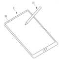
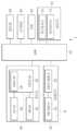
도 1a 및 도 1b는 스타일러스 펜과 전자 디바이스를 나타낸 개념도이다.1A and 1B are conceptual views illustrating a stylus pen and an electronic device.
도 1a를 참조하면, 스타일러스 펜(10)은 전자 디바이스(2)의 터치 스크린(20) 근처에서 전자 디바이스(2) 또는 터치 스크린(20)으로부터 출력되는 신호를 수신하고, 터치 스크린(20)에 신호를 송신할 수 있다.Referring to FIG. 1A, the
도 1b를 참조하면, 전자 디바이스(2)는 폴더블(foldable)하다. 스타일러스 펜(10)은 폴더블 전자 디바이스(2)의 터치 스크린(20) 근처에서 전자 디바이스(20) 또는 터치 스크린(20)으로부터 출력되는 신호를 수신하고, 터치 스크린(20)에 신호를 송신할 수 있다.Referring to FIG. 1B , the
직사각형 형상의 폴더블 전자 디바이스(2) 또는 그에 포함되는 터치 스크린(20) 등의 부재에서, 평면상 좌측에 위치하는 장변을 제1 장변(LS1), 우측에 위치하는 장변을 제2 장변(LS2), 위쪽에 위치하는 단변을 제1 단변(SS1), 아래쪽에 위치하는 단변을 제2 단변(SS2)으로 지칭하기로 한다.In a member such as the rectangular foldable
폴더블 전자 디바이스(2)는 제1 단변(SS1) 및 제2 단변(SS2)을 가로지르는 폴딩축(AXIS_F)을 기준으로 소정의 폴딩 방향을 따라 구부러질 수 있다. 즉, 폴더블 전자 디바이스(2)는 폴딩축(AXIS_F)을 기준으로 폴딩 방향을 따라 접힌 상태(folded state)와 펼쳐진 상태(unfolded state) 간의 상태 전환이 가능할 수 있다.The foldable
도 2는 스타일러스 펜과 전자 디바이스 사이의 신호 전달 동작을 개략적으로 나타낸 도면이다. 도 2의 (a)를 참조하면, 터치 스크린(20a)은 디지타이저(29), 디스플레이 패널(251), 터치 전극층(21), 및 윈도우(22)를 포함한다.2 is a diagram schematically illustrating a signal transfer operation between a stylus pen and an electronic device. Referring to (a) of FIG. 2 , the
패시브 스타일러스 펜 중 EMR(Electro-Magnetic Resonance) 방식의 펜의 경우, 디지타이저(digitizer)(29)가 EMR 방식의 스타일러스 펜(10a)에 자기 신호(B)를 전달하면, 스타일러스 펜(10a)에 포함된 공진 회로가 자기 신호(B)에 공진한다. 그러면, 디지타이저(33)가 스타일러스 펜(10a)으로부터 공진된 자기 신호(B)를 입력받는다.In the case of an EMR (Electro-Magnetic Resonance) type pen among passive stylus pens, when a
디지타이저(29)는 디스플레이 패널(251) 아래에 부착될 수 있으며, 도전성의 안테나 루프가 복수로 형성되어 있는 FPCB(Flexible Printed Circuit Board)와 안테나 루프에 의해 생성된 자기장을 차단하고, 안테나 루프가 자기장을 형성할 때 다른 전기적 소자, 구성요소에서 생성될 수 있는 와전류를 차단하는 페라이트 시트(ferrite sheet)를 포함한다.The
FPCB에는 공진 신호가 입력되는 위치를 감지하기 위한 복수의 안테나 루프가 복수의 레이어로 구성된다. 하나의 안테나 루프는 적어도 하나의 다른 안테나 루프와 Z축 방향으로 중첩한 형태를 가진다. 이에 의해 FPCB의 두께가 두껍다. 따라서, 디지타이저(29)를 사용하는 경우 전자 디바이스(2)의 박형화, 소형화에 어려움이 있다.In the FPCB, a plurality of antenna loops for detecting a position where a resonance signal is input are composed of a plurality of layers. One antenna loop overlaps at least one other antenna loop in the Z-axis direction. As a result, the thickness of the FPCB is thick. Therefore, when using the
이러한 디지타이저(29)가 폴더블/플렉서블 전자 디바이스(2)에 탑재되는 경우, 접힘이 발생할 때 폴딩되는 영역에 부착된 FPCB에 변형이 발생할 수 있다. 반복적인 접힘에 의해 안테나 루프를 형성하는 배선 부재에 스트레스가 가해지고, 결국 배선 부재의 손상을 가져올 수 있다. 페라이트 시트는 안테나 루프에 의해 발생된 자기장이 전자 디바이스(2) 내부에 미치는 영향을 차단한다. 페라이트 시트도 두께가 두껍고, 전자 디바이스(2)의 접힘이 발생할 때 변형이 발생되기 쉬우며, 반복적인 접힘에 의해 손상될 수 있다.When such a
도 2의 (b)를 참조하면, 터치 스크린(20c)은 디스플레이 패널(251), 터치 전극층(21), 및 윈도우(22)를 포함한다.Referring to (b) of FIG. 2 , the
공진 회로를 포함하는 스타일러스 펜(10)의 경우, 터치 전극층(21)의 전극이 스타일러스 펜(10)에 자기 신호(B)를 전달하면, 스타일러스 펜(10)에 포함된 공진 회로가 자기 신호(B)에 공진한다. 그러면, 터치 전극층(21)의 전극이 스타일러스 펜(10)으로부터 공진된 전자기 신호(E 및/또는 B)를 입력받을 수 있다. 저항이 작은 메탈 메시(metal mesh)로 터치 전극층(21)의 전극이 형성되는 경우, 스타일러스 펜(10)으로부터의 자기 신호의 검출이 가능하다.In the case of the
마찬가지로, 디지타이저(29)와 비교하면, 터치 스크린(20c)은 자기 신호를 스타일러스 펜(10)에 전달하기 위한 추가적인 유닛이나 모듈을 필요로 하지 않으므로, 터치 스크린(20b)의 박형화가 가능하고, 제조 비용에 있어서도 장점이 있다.Similarly, compared to the
도 2의 (c)를 참조하면, 터치 스크린(20b)은 루프 코일(264), 디스플레이 패널(251), 터치 전극층(21), 및 윈도우(22)를 포함한다.Referring to (c) of FIG. 2 , the
공진 회로를 포함하는 스타일러스 펜(10)의 경우, 루프 코일(264)이 스타일러스 펜(10)에 자기 신호(B)를 전달하면, 스타일러스 펜(10)에 포함된 공진 회로가 자기 신호(B)에 공진한다. 그러면, 터치 전극층(21)의 전극이 스타일러스 펜(10)으로부터 공진된 전자기 신호(E 및/또는 B)를 입력받을 수 있다.In the case of a
디지타이저(29)와 비교하면, 루프 코일(264)은 터치 위치를 검출하기 위한 자기 신호(B)를 수신하지 않으므로, 배선 구조가 간단하여 터치 스크린(20b)의 박형화가 가능하다. 이로써, 전자 디바이스(2)의 박형화, 소형화가 가능하다. 또한, 루프 코일(264)은 다양한 크기로 다양한 위치에 형성될 수 있으므로, 이러한 터치 스크린(20b)은 폴더블/플렉서블 전자 디바이스(2)에도 적용이 가능하다.Compared to the
루프 코일(264)은 안테나 루프가 위치한 기판과 및 페라이트 시트를 포함할 수 있다. 안테나 루프는 구리, 은 등과 같은 도체 재료로 형성될 수 있다. 안테나 루프는 기판 외에도 터치 전극층(21)과 동일한 층에 위치할 수 있고, 이 경우, 안테나 루프는 메탈 메시, ITO, 그래핀, 실버 나노 와이어 등과 같은 높은 투과율, 저 임피던스를 나타내는 도체 재료로 형성될 수 있다. 또한 안테나 루프는 윈도우 아래에 위치할 수 있고, 이 경우 기판은 루프 코일(264)에 포함되지 않을 수 있다.The
상기에서 터치 전극층(21)은 제1 방향의 터치 좌표를 검출하기 위한 복수의 제1 터치 전극과 제1 방향과 교차하는 제2 방향의 터치 좌표를 검출하기 위한 복수의 제2 터치 전극을 포함할 수 있다. 도 2에서 터치 전극층(21)이 하나의 층으로 도시되었으나, 제1 터치 전극과 제2 터치 전극은 서로 상이한 층에 각각 위치할 수도 있고, 서로 중첩하여 위치할 수도 있고, 서로 중첩하여 위치하지 않을 수도 있고, 제1 터치 전극과 제2 터치 전극 사이에 별도의 층이 개재되어 있을 수도 있으며, 이에 제한되지 않는다.In the above, the
도 2의 (d)를 참조하면, 터치 스크린(20d)은 디스플레이 패널(251), 터치 전극층(21), 및 윈도우(22)를 포함한다.Referring to (d) of FIG. 2 , the
공진 회로를 포함하는 액티브 스타일러스 펜(10')의 경우, 액티브 스타일러스 펜(10')에 포함된 공진 회로는 액티브 스타일러스 펜(10') 내의 전원(예를 들어, 전력을 저장하기 위한 배터리(이차 전지를 포함함) 및 EDLC(electric double layered capacitor)와 같은 커패시터)을 사용하여 공진한다. 그러면, 터치 전극층(21)의 전극이 스타일러스 펜(10')으로부터 공진된 전자기 신호(E 및/또는 B)를 입력받을 수 있다. 저항이 작은 메탈 메시로 터치 전극층(21)의 전극이 형성되는 경우, 스타일러스 펜(10')으로부터의 자기 신호의 검출이 가능하다. 액티브 스타일러스 펜(10')은 전자기 신호를 생성하기 위해 공진 회로뿐만 아니라, 전원을 사용하여 소정 주파수를 갖는 전자기 신호(E 및/또는 B)를 출력하는 회로를 포함할 수 있다. 또한, 액티브 스타일러스 펜(10')은 공진 회로와 소정 주파수를 갖는 전자기 신호(E 및/또는 B)를 출력하는 회로를 모두 포함할 수도 있다.In the case of an active stylus pen 10' including a resonant circuit, the resonant circuit included in the active stylus pen 10' is a power source in the active stylus pen 10' (eg, a battery for storing power (a secondary battery) including batteries) and capacitors such as EDLC (electric double layered capacitor) to resonate. Then, the electrodes of the
터치 스크린(20d)은 자기 신호를 스타일러스 펜(10')에 전달하지 않고도 스타일러스 펜(10')으로부터 전자기 신호를 수신할 수 있다. 즉, 터치 스크린(20d)은 스타일러스 펜(10')에 포함된 공진 회로를 공진시키기 위한 신호를 생성하기 위한 추가적인 유닛이나 모듈을 필요로 하지 않으므로, 터치 스크린(20d)의 박형화, 소형화가 가능하고, 소비 전력과 제조 비용에 있어서도 장점이 있다.The
다음으로 도 3a 내지 도 3c를 참조하여, 도 2의 (b)의 터치 스크린(20b)의 구조에 대해 상세하게 설명한다.Next, the structure of the
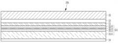
도 3a는 도 1a의 전자 디바이스의 일부 적층 구조를 개략적으로 나타낸 도면이다.FIG. 3A is a schematic diagram of a partial stacked structure of the electronic device of FIG. 1A.
도 3a를 참조하면, 디스플레이 패널(251)은 기판(2510) 상에 배치된 회로 구동층(2512)을 포함할 수 있다. 회로 구동층(2512)은 영상을 표시하는 화소의 발광층(2514)을 구동하는 회로를 포함할 수 있다. 예를 들어, 회로 구동층(2512)은 복수의 박막 트랜지스터와 커패시터를 포함할 수 있다.Referring to FIG. 3A , the
회로 구동층(2512) 상에는 발광층(2514)이 배치될 수 있다. 발광층(2514)은 유기 발광층을 포함할 수 있다. 발광층(2514)은 회로 구동층(2512)에서 전달하는 구동 신호에 따라 다양한 휘도로 발광할 수 있다.An
발광층(2514) 상에는 공통 전극층(2516)이 배치될 수 있다. 공통 전극층(2516)은 슬릿 형태의 적어도 하나의 개구를 가질 수 있다.A
공통 전극층(2516) 상에는 봉지층(2516)이 배치될 수 있다. 봉지층(2516)은 무기막 또는 무기막과 유기막의 적층막을 포함할 수 있다. 다른 예로 봉지층(2516)으로 글래스나 봉지 필름 등이 적용될 수도 있다.An
봉지층(2516) 상에는 터치 전극층(21) 또는 터치 전극 등이 배치될 수 있다. 터치 전극층(21)은 터치 입력을 인지하는 층으로서, 터치 부재의 기능을 수행할 수 있다. 터치 전극층(21)은 복수의 터치 영역과 터치 전극들을 포함할 수 있다.A
터치 전극층(21) 상에는 편광층(23)이 배치될 수 있다. 편광층(23)은 외광 반사를 줄이는 역할을 할 수 있다. 편광층(23)은 점착층을 통해 터치 전극층(21)상에 부착될 수 있다. 편광층(23)은 생략될 수도 있다.A
편광층(23) 상에는 보호층(22)이 배치될 수 있다. 보호층(22)은 예컨대 윈도우 부재를 포함할 수 있다. 보호층(22)은 광학 투명 접착제 등에 의해 편광층(23) 상에 부착될 수 있다.A
디스플레이 패널(251)의 아래에는 자기장 차폐층(24)이 배치될 수 있다. 자기장 차폐층(24)은 자기장을 차단하는 페라이트 시트를 포함할 수 있다. 이외에도 자기장 차폐층(24)은 기판(2510) 아래에 접착된 페라이트 분말을 포함할 수 있다. 자기장 차폐층(24)은 터치 전극층(21) 및/또는 스타일러스 펜(10)이 자기장을 형성할 때 다른 전기적 소자, 구성요소에서 생성될 수 있는 와전류를 차단할 수 있다.A magnetic
도 3b 및 도 3c는 도 1b의 전자 디바이스의 일부 적층 구조를 개략적으로 나타낸 도면이다.3B and 3C are diagrams schematically illustrating a partial stacked structure of the electronic device of FIG. 1B.
도 3b의 적층 구조는 도 3a의 적층 구조와 동일하나, 폴딩축(AXIS_F)을 기준으로 폴더블 전자 디바이스(2)의 접힘이 발생할 때 폴딩되는 영역(이하, 폴딩 영역)(FA)에 자기장 차폐층(24)이 위치할 수 있다.The stacked structure of FIG. 3B is the same as the stacked structure of FIG. 3A , but the magnetic field is shielded in the folded area (hereinafter referred to as the folding area) FA when the foldable
도 3c의 적층 구조는 도 3b의 적층 구조와 비교하여, 폴딩 영역(FA) 또는 폴딩 영역(FA)에 포함된 일 영역을 제외하고 자기장 차폐층(24)이 위치할 수 있다. 예를 들어, 자기장 차폐층(24)은 폴딩 영역(FA)과 장변(LS1) 사이의 영역에 위치한 제1 시트(24a) 및 폴딩 영역(FA)과 장변(LS2) 사이의 영역에 위치한 제2 시트(24b)를 포함할 수 있다. 자기장 차폐층(24)은 두 개의 시트 외에 복수의 시트를 포함할 수 있으며, 이 경우에도 자기장 차폐층(24)은 디스플레이 패널(251) 후면의 폴딩 영역(FA)을 제외한 영역 또는 폴딩 영역(FA)의 일부를 제외한 영역에 위치할 수 있다.Compared to the stacked structure of FIG. 3B , the magnetic
다음으로 도 4를 참조하여, 실시예들에 따른 전자 디바이스(2)에 대해 설명한다.Next, referring to FIG. 4 , an
도 4는 전자 디바이스를 개략적으로 나타낸 블록도이다.4 is a schematic block diagram of an electronic device.
도시된 바와 같이, 전자 디바이스(2)는 무선 통신부(210), 메모리(220), 인터페이스부(230), 전원공급부(240), 디스플레이부(250), 터치 모듈(260), 및 제어부(270) 등을 포함할 수 있다. 도 4에 도시된 구성요소들은 전자 디바이스를 구현하는데 있어서 필수적인 것은 아니어서, 본 개시 상에서 설명되는 전자 디바이스는 위에서 열거된 구성요소들 보다 많거나, 또는 적은 구성요소들을 가질 수 있다.As shown, the
보다 구체적으로, 상기 구성요소들 중 무선 통신부(210)는, 전자 디바이스(2)와 무선 통신 시스템 사이, 전자 디바이스(2)와 다른 전자 디바이스(2) 사이, 또는 전자 디바이스(2)와 외부서버 사이의 무선 통신을 가능하게 하는 하나 이상의 모듈을 포함할 수 있다. 또한, 상기 무선 통신부(210)는, 전자 디바이스(2)를 하나 이상의 네트워크에 연결하는 하나 이상의 모듈을 포함할 수 있다.More specifically, among the components, the
이러한 무선 통신부(210)는, 무선 인터넷 모듈(211) 및 근거리 통신 모듈(212) 등을 포함할 수 있다.Such a
무선 인터넷 모듈(211)은 무선 인터넷 접속을 위한 모듈을 말하는 것으로, 전자 디바이스(2)에 내장될 수 있다. 무선 인터넷 모듈(211)은 무선 인터넷 기술들에 따른 통신망에서 무선 신호를 송수신하도록 이루어진다. 무선 인터넷 기술로는, 예를 들어 WLAN(Wireless LAN), Wi-Fi(Wireless-Fidelity), Wi-Fi(Wireless Fidelity) Direct, DLNA(Digital Living Network Alliance), WiBro(Wireless Broadband), WiMAX(World Interoperability for Microwave Access), HSDPA(High Speed Downlink Packet Access), HSUPA(High Speed Uplink Packet Access), NR(New Radio), LTE(Long Term Evolution), LTE-A(Long Term Evolution-Advanced) 등이 있으며, 상기 무선 인터넷 모듈(211)은 상기에서 나열되지 않은 인터넷 기술까지 포함한 범위에서 적어도 하나의 무선 인터넷 기술에 따라 데이터를 송수신하게 된다.The
근거리 통신 모듈(212)은 근거리 통신(Short range communication)을 위한 것으로서, 블루투스(Bluetooth??), RFID(Radio Frequency Identification), 적외선 통신(Infrared Data Association; IrDA), UWB(Ultra Wideband), ZigBee, NFC(Near Field Communication), Wi-Fi, Wi-Fi Direct, Wireless USB(Wireless Universal Serial Bus) 기술 중 적어도 하나를 사용하여, 근거리 통신을 지원할 수 있다. 이러한, 근거리 통신 모듈(212)은, 근거리 무선 통신망(Wireless Area Networks)을 통해 전자 디바이스(2)와 무선 통신 시스템 사이, 전자 디바이스(2)와 무선 통신 가능 디바이스 사이, 또는 전자 디바이스(2)와 외부 서버가 위치한 네트워크 사이의 무선 통신을 지원할 수 있다. 상기 근거리 무선 통신망은 근거리 무선 개인 통신망(Wireless Personal Area Networks)일 수 있다.The short
여기서, 무선 통신 가능 디바이스는 본 발명에 따른 전자 디바이스(2)와 데이터를 상호 교환하는 것이 가능한(또는 연동 가능한) 이동 단말기(mobile terminal, 예를 들어, 스마트 폰, 태블릿 PC, 노트북(notebook) 등)가 될 수 있다. 근거리 통신 모듈(212)은, 전자 디바이스(2) 주변에, 상기 전자 디바이스(2)와 통신 가능한 무선 통신 가능 디바이스를 감지(또는 인식)할 수 있다. 나아가, 제어부(270)는 상기 감지된 무선 통신 가능 디바이스가 일 실시예에 따른 전자 디바이스(2)와 통신하도록 인증된 디바이스인 경우, 전자 디바이스(2)에서 처리되는 데이터의 적어도 일부를, 상기 근거리 통신 모듈(212)을 통해 무선 통신 가능 디바이스로 전송할 수 있다. 따라서, 무선 통신 가능 디바이스의 사용자는, 전자 디바이스(2)에서 처리되는 데이터를, 무선 통신 가능 디바이스를 통해 이용할 수 있다.Here, the wireless communication capable device is a mobile terminal (eg, a smart phone, a tablet PC, a notebook, etc.) capable of exchanging (or interlocking) data with the
또한, 메모리(220)는 전자 디바이스(2)의 다양한 기능을 지원하는 데이터를 저장한다. 메모리(220)는 전자 디바이스(2)에서 구동되는 다수의 응용 프로그램(application program 또는 애플리케이션(application)), 전자 디바이스(2)의 동작을 위한 데이터들, 명령어들을 저장할 수 있다.Also, the
인터페이스부(230)는 전자 디바이스(2)에 연결되는 다양한 종류의 외부 기기와의 통로 역할을 수행한다. 이러한 인터페이스부(230)는, 유/무선 헤드셋 포트(port), 외부 충전기 포트(port), 유/무선 데이터 포트(port), 메모리 카드(memory card) 포트, 식별 모듈이 구비된 장치를 연결하는 포트(port), 오디오 I/O(Input/Output) 포트(port), 비디오 I/O 포트(port), 이어폰 포트(port) 중 적어도 하나를 포함할 수 있다.The
전원공급부(240)는 제어부(270)의 제어 하에서, 외부의 전원, 내부의 전원을 인가 받아 전자 디바이스(2)에 포함된 각 구성요소들에 전원을 공급한다. 이러한 전원공급부(240)는 배터리를 포함하며, 상기 배터리는 내장형 배터리 또는 교체가능한 형태의 배터리가 될 수 있다.The
디스플레이부(250)는 전자 디바이스(2)에서 처리되는 정보를 표시(출력)한다. 예를 들어, 디스플레이부(250)는 전자 디바이스(2)에서 구동되는 응용 프로그램의 실행화면 정보, 또는 이러한 실행화면 정보에 따른 UI(User Interface), GUI(Graphic User Interface) 정보를 표시할 수 있다.The
디스플레이부(250)는 LCD 디스플레이(liquid crystal display), OLED(organic light-emitting diode) 디스플레이, 전자잉크 디스플레이(e-ink display), 양자점(quantum-dot) 발광 디스플레이, 마이크로 LED(Light emitting diode) 디스플레이 등을 포함할 수 있다.The
디스플레이부(250)는 영상을 표시하는 디스플레이 패널(251)과, 디스플레이 패널(251)과 연결되어 영상을 표시하기 위한 신호들을 디스플레이 패널(251)로 공급하는 디스플레이 컨트롤러(252)를 포함한다. 예를 들어, 디스플레이 패널(251)에는 복수의 스캔선, 복수의 데이터선과 같은 신호선들에 연결된 복수의 화소와, 스캔선으로 스캔 신호를 공급하는 스캔 구동/수신부가 위치할 수 있고, 디스플레이 컨트롤러(252)는 데이터선으로 인가하는 데이터 신호를 생성하는 데이터 구동 IC와 영상 신호를 처리하여 디스플레이부(250)의 전반적인 동작을 제어하는 타이밍 컨트롤러, 전원 관리(power management) IC 등을 포함할 수 있다.The
터치 모듈(260)은 정전용량 방식을 이용하여 터치 영역에 가해지는 터치(또는 터치 입력)를 감지한다. 일 예로서, 터치 모듈(260)은, 특정 부위에 발생하는 정전 용량, 전압, 또는 전류 등의 변화를 전기적인 입력신호로 변환하도록 구성될 수 있다. 터치 모듈(260)은, 터치 영역 상에 터치를 가하는 터치 객체가 터치 모듈(260) 상에 터치 되는 위치, 면적, 터치 시의 정전 용량 등을 검출할 수 있도록 구성될 수 있다. 여기에서, 터치 객체는 상기 터치 센서에 터치를 인가하는 물체로서, 예를 들어, 사용자의 신체 부위(손가락, 손바닥 등), 패시브(passive) 또는 액티브(active) 방식의 스타일러스 펜(10) 등이 될 수 있다.The
터치 모듈(260)은 터치 전극이 위치하는 터치 센서(261)와 터치 센서(261)에 구동 신호를 인가하고 터치 센서(261)로부터 감지 신호를 수신하여, 제어부(270) 및/또는 디스플레이 컨트롤러(252)에 터치 데이터를 전달하는 터치 컨트롤러(262)를 포함한다.The
터치 컨트롤러(262)는 복수의 제1 터치 전극 중 적어도 하나에 연결되어 구동 신호를 인가하고 감지 신호를 수신하는 제1 구동/수신부, 복수의 제2 터치 전극 중 적어도 하나에 연결되어 구동 신호를 인가하고 감지 신호를 수신하는 제2 구동/수신부, 및 제1 구동/수신부와 제2 구동/수신부의 동작을 제어하고, 제1 및 제2 구동/수신부로부터 출력되는 감지 신호를 사용하여 터치 위치를 획득하는 MCU(micro control unit)를 포함할 수 있다.The
디스플레이 패널(251)과 터치 센서(261)는 상호 레이어 구조를 이루거나 일체형으로 형성되어, 터치 스크린(20)으로 지칭될 수 있다.The
제어부(270)는 전자 디바이스(2)의 구동을 제어하며, 전자 디바이스(2)의 터치 감지 결과에 대응하여 터치 좌표 정보를 출력할 수 있다. 또한, 제어부(270)는 터치 감지 결과에 대응하여 구동 신호의 주파수를 변경할 수 있다.The
제어부(270)는 상기 응용 프로그램과 관련된 동작 외에도, 통상적으로 전자 디바이스(2)의 전반적인 동작을 제어한다. 제어부(270)는 위에서 살펴본 구성요소들을 통해 입력 또는 출력되는 신호, 데이터, 정보 등을 처리하거나 메모리(220)에 저장된 응용 프로그램을 구동함으로써, 사용자에게 적절한 정보 또는 기능을 제공 또는 처리할 수 있다.The
또한, 제어부(270)는 메모리(220)에 저장된 응용 프로그램을 구동하기 위하여, 도 4와 함께 살펴본 구성요소들 중 적어도 일부를 제어할 수 있다. 나아가, 제어부(270)는 상기 응용 프로그램의 구동을 위하여, 전자 디바이스(2)에 포함된 구성요소들 중 적어도 둘 이상을 서로 조합하여 동작시킬 수 있다.In addition, the
상기에서 터치 모듈(260)이 디스플레이부(250)와 함께 전자 디바이스(2)에 포함되는 것으로 설명하였으나, 전자 디바이스(2)는 터치 모듈(260)만을 포함할 수도 있다.Although the
도 5는 실시예들에 따른 스타일러스 펜을 나타낸 도면이다.5 is a view showing a stylus pen according to embodiments.
도 5의 스타일러스 펜들은 공통적으로 하우징 내의 공진 회로부(12)를 포함한다.The stylus pens of FIG. 5 commonly include a
공진 회로부(12)는 LC 공진 회로로서, 터치 스크린(20)에서 출력되는 구동 신호에 공진할 수 있다. 구동 신호는, 공진 회로부(12)의 공진 주파수에 대응하는 주파수를 갖는 신호(예를 들어, 사인파, 구형파 등)를 포함할 수 있다. 공진을 위해서는 공진 회로부(12)의 공진 주파수와 구동 신호의 주파수가 동일 내지는 매우 유사해야 한다. 스타일러스 펜(10a, 10b)의 공진 주파수는 스타일러스 펜(10a, 10b)의 공진 회로부(12)의 설계 값에 따른다. 도 2의 (b)의 전극(21) 또는 도 2의 (c)의 루프 코일(264)이 구동 신호에 의한 전자기장을 발생시키면, 스타일러스 펜(10a, 10b)의 공진 회로부(12)는 자기장의 변화를 통해 수신한 신호를 이용하여 공진한다.The
스타일러스 펜(10a, 10b)의 소자들은 하우징에 수용될 수 있다. 하우징은 원기둥, 다각기둥, 적어도 일부분이 곡면인 기둥 형태, 배흘림기둥(entasis) 형태, 각뿔대(frustum of pyramid) 형태, 원뿔대(circular truncated cone) 형태 등을 가질 수도 있으며, 그 형태에 제한되지 않는다. 하우징은 내부가 비어있으므로, 그 내부에 공진 회로부(12)와 같은 스타일러스 펜(10a, 10b)의 소자를 수용할 수 있다. 이러한 하우징은 비전도성 물질로 이루어질 수 있다.Elements of the stylus pens 10a and 10b may be accommodated in the housing. The housing may have a cylindrical shape, a polygonal column shape, a column shape in which at least a portion is curved, an entasis shape, a frustum of pyramid shape, a circular truncated cone shape, and the like, but is not limited thereto. Since the inside of the housing is empty, elements of the stylus pens 10a and 10b such as the
도 5의 (a)에 도시된 바와 같이, EMR 방식의 스타일러스 펜(10a)은 심체(11a)과 공진 회로부(12)를 포함한다. 공진 회로부(12)는 인덕터부(14)와 커패시터부(13)를 포함한다. 인덕터부(14)는 심체(11a)가 관통하는 페라이트 코어(115)와 페라이트 코어(115)의 외면에 권선된 코일(116)을 포함한다.As shown in (a) of FIG. 5, the EMR-
심체(11a)는 한쪽의 단부가, 펜 끝으로서, 페라이트 코어(115)로부터 돌출된다. 심체(11a)는, 도체, 예를 들면 도전성 금속이나 도전성 분말을 혼입한 경질 수지로 이루어지는 전극심으로 구성될 수 있다.One end of the
페라이트 코어(115)에는, 예를 들면 원기둥 모양 형상의 페라이트 재료에, 심체(11a)를 삽입 통과시키기 위한 소정의 지름(예를 들면 1㎜)의 축심 방향의 관통공이 형성되어 있다.In the
코일(116)은 페라이트 코어(115)의 축심 방향의 전체 길이에 걸쳐 권선될 수 있거나, 일부 길이에 걸쳐 권선될 수 있다. 코일(116)은 커패시터부(13)에 전기적으로 연결된다.The
커패시터부(13)는 병렬로 연결된 복수의 커패시터를 포함할 수 있다. 프린트 기판 상의 각 커패시터는 서로 상이한 커패시턴스를 가질 수 있으며, 제조 공정 내에서 트리밍(trimming)될 수 있다.The
도 5의 (b)에 도시된 바와 같이, ECR(Electrically Coupled Resonance) 방식의 스타일러스 펜(10b)은 전도성 팁(11b)과 공진 회로부(12)를 포함한다. 공진 회로부(12)는 인덕터부(14)와 커패시터부(13)를 포함한다. 인덕터부(14)는 페라이트 코어(115)와 페라이트 코어(115)의 외면에 권선된 코일(116)을 포함한다.As shown in (b) of FIG. 5, an electrically coupled resonance (ECR)
전도성 팁(11b)은 적어도 일부가 전도성 물질(예를 들어, 금속, 전도성 고무, 전도성 패브릭, 전도성 실리콘 등)로 형성될 수 있으며, 이에 제한되지 않는다.At least a portion of the
코일(116)은 페라이트 코어(115)의 축심 방향의 전체 길이에 걸쳐 권선될 수 있거나, 일부 길이에 걸쳐 권선될 수 있다. 코일(116)은 커패시터부(13)에 전기적으로 연결된다.The
커패시터부(13)는 병렬로 연결된 복수의 커패시터를 포함할 수 있다. 프린트 기판 상의 각 커패시터는 서로 상이한 커패시턴스를 가질 수 있으며, 제조 공정 내에서 트리밍(trimming)될 수 있다.The
이하에서는, 도 5에서 설명한 스타일러스 펜으로부터의 공진 신호를 사용하여 터치를 검출하는 방법에 대해 설명한다.Hereinafter, a method of detecting a touch using the resonance signal from the stylus pen described in FIG. 5 will be described.
도 6은 일 실시예에 따른 터치 디바이스의 일부를 개략적으로 나타낸 도면이다.6 is a diagram schematically illustrating a portion of a touch device according to an exemplary embodiment.
일 실시예에 따른 터치 모듈(즉, 터치 디바이스)(260)은 터치 센서(261) 및 터치 센서(261)를 제어하는 터치 컨트롤러(262)를 포함한다. 터치 컨트롤러(262)는 터치 센서(261)와 신호를 송수신하는 제1 구동/수신부(2620) 및 제2 구동/수신부(2622), 및 제어부(2624)를 포함할 수 있다.The touch module (ie, touch device) 260 according to an embodiment includes a
터치 센서(261)는 제1 방향의 터치 좌표를 검출하기 위한 복수의 제1 터치 전극(111-1 내지 111-m)과 제1 방향과 교차하는 제2 방향의 터치 좌표를 검출하기 위한 복수의 제2 터치 전극(121-1 내지 121-n)을 포함할 수 있다. 예를 들어, 복수의 제1 터치 전극(111-1 내지 111-m)은 제2 방향으로 연장된 형태를 가질 수 있고, 복수의 제2 터치 전극(121-1 내지 121-n)은 제1 방향으로 연장된 형태를 가질 수 있다. 터치 센서(261) 내에서, 복수의 제1 터치 전극(111-1 내지 111-m)은 제1 방향을 따라 배열될 수 있고, 복수의 제2 터치 전극(121-1 내지 121-n)은 제2 방향을 따라 배열될 수 있다.The
제1 구동/수신부(2620)는 복수의 제1 터치 전극(111-1 내지 111-m)에 구동 신호를 인가할 수 있다. 제2 구동/수신부(2622)는 복수의 제2 터치 전극(121-1 내지 121-n)으로부터 감지 신호를 수신할 수 있다.The first driving/
상기에서 터치 센서(261)가 상호 커패시턴스 방식으로 구현되는 것으로 설명하였으나, 터치 센서(261)는 셀프 커패시턴스 방식으로 구현될 수 있으며, 상호 커패시턴스 방식에서의 터치 전극들(111-1 내지 111-m, 121-1 내지 121-n), 제1 구동/수신부(2620), 및 제2 구동/수신부(2622)를 적절히 변형하거나, 새로운 컴포넌트를 추가하거나, 일부 구성요소를 생략하여 셀프 커패시턴스 방식에 적합하도록 수정하는 것은 통상의 기술자에게 용이할 것이다.Although the
즉, 터치 센서(261)는 셀프 커패시턴스 방식의 터치 전극을 복수로 포함할 수 있으며, 이 경우, 터치 전극들은 도트(dot) 형태로 배열될 수도 있고, 상기에서 설명한 바와 같이 일 방향으로 연장된 형태로도 배열될 수 있다.That is, the
다음으로 도 7을 참조하여 전극 및 트레이스에 대해 설명한다.Next, electrodes and traces will be described with reference to FIG. 7 .
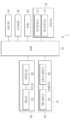
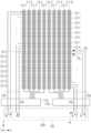
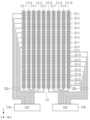
도 7은 일 실시예에 따른 터치 디바이스의 전극 및 트레이스의 배치 형태의 일례를 나타낸 도면이다.7 is a diagram illustrating an example of an arrangement form of electrodes and traces of a touch device according to an exemplary embodiment.
터치 센서는 터치 전극들(111, 121)과 더미 전극이 연결된 안테나를 포함할 수 있다. 예를 들어, 복수의 더미 전극(121D)이 터치 전극들(111, 121)과 동일한 층에 위치하고, 복수의 더미 전극(121D) 중 일부가 브릿지(121B)에 의해 서로 연결될 수 있다. 브릿지(121B)는 트레이스(112)를 통해 패드(113a, 113b)에 연결될 수 있다.The touch sensor may include an antenna to which the
터치 컨트롤러(262)는 스타일러스 펜(10)을 공진시키기 위해 안테나(121A)에 구동 신호를 인가할 수 있다. 구동 신호는, 공진 회로부(12)의 공진 주파수에 대응하는 주파수를 갖는 신호(예를 들어, 사인파, 구형파 등)를 포함할 수 있으며, 소정 주파수를 갖는 교류 전압 또는 교류 전류일 수 있다. 이러한 구동 신호의 주파수와 크기는 제어부(2624)의 제어에 따라 변경될 수 있다. 구체적으로, 터치 컨트롤러(262)는 인접한 두 브릿지(121B) 중 하나에 구동 신호를 인가하고, 다른 하나를 접지시킬 수 있다.The
터치 전극들(111, 121)은 터치 영역의 가장자리에 위치하는 주변 영역의 트레이스들(112, 122a, 122b)을 통해 패드들(113a, 113b)에 연결되어 있다. 제1 터치 전극들(111-1, 111-2, 111-3, ...)은 각각의 트레이스들(112)에 대응하여 연결되어 있고, 제2 터치 전극들(121-1, 121-2, 121-3, ...)은 각각의 트레이스들(122a, 122b)에 대응하여 연결되어 있다.The
터치 전극들(111, 121)과 트레이스들(112, 122a, 122b)은 동일한 층으로 형성될 수 있다. 터치 전극들(111, 121)과 트레이스들(112, 122a, 122b)은 메탈 메시, 실버 나노 와이어와 같은 높은 투과율, 저 임피던스를 나타내는 도체 재료로 형성될 수 있다. 그러나, 터치 전극들(111, 121)과 트레이스들(112, 122a, 122b)은 상이한 층으로 위치할 수 있으며, ITO, 그래핀으로 제조될 수 있으며, 이에 제한되지 않는다.The
패드들(113a, 113b)은 터치 컨트롤러(262)에 접속되어 있으며, 터치 컨트롤러(262)의 신호(예컨대, 구동 신호)를 터치 전극들(111, 121)에 전달하고, 터치 전극들(111, 121)로부터의 신호(예컨대, 감지 신호)를 터치 컨트롤러(262)에 전달한다.The
도 8은 일 실시예에 따른 터치 디바이스의 전극 및 트레이스의 배치 형태의 다른 예를 나타낸 도면이다.8 is a diagram illustrating another example of an arrangement form of electrodes and traces of a touch device according to an exemplary embodiment.
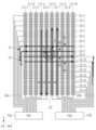
도 7과 마찬가지로, 터치 전극들(111, 121)은 터치 영역의 가장자리에 위치하는 주변 영역의 트레이스들(112, 122a, 122b)을 통해 패드들(113a, 113b)에 연결되어 있다.As in FIG. 7 , the
하나의 터치 전극은 두 개의 신호 입력단을 가지며, 두 개의 신호 입력단은 두 개의 트레이스에 대응하여 연결되어 있다. 예를 들어, 제2 터치 전극(121-9)는 "U"자 형태의 전극으로서, 상측에 위치한 제1 신호 입력단(TE1)과 하측에 위치한 제2 신호 입력단(TE2)을 가진다.One touch electrode has two signal input terminals, and the two signal input terminals are connected to correspond to two traces. For example, the second touch electrode 121 - 9 is a "U" shaped electrode and has a first signal input terminal TE1 located on the upper side and a second signal input terminal TE2 located on the lower side.
두 개의 신호 입력단 중 하나는 스위치를 통해 접지에 연결되거나 또는 구동/수신부(2620)에 연결될 수 있다. 예를 들어, 제1 신호 입력단(TE1)은 구동/수신부(2620)에 연결되어 있고, 제2 신호 입력단(TE2)은 스위치(SW)에 연결되어 있다. 스위치(SW)는 제2 신호 입력단(TE2)을 접지 또는 구동/수신부(2620)에 연결시킨다.One of the two signal input terminals may be connected to ground through a switch or connected to the driving/
터치 컨트롤러(262)는 스타일러스 펜(10)을 공진시키기 위해 하나의 신호 입력단을 접지에 연결시키고 구동 신호를 인가할 수 있다. 터치 컨트롤러(262)는 두 신호 입력단으로부터 동시에 감지 신호를 수신할 수 있다. 또한, 일반적인 핑거 터치를 위한 구동 시에는 터치 컨트롤러(262)는 두 신호 입력단에 동일한 위상의 구동 신호를 인가할 수도 있다.The
상기에서 하나의 신호 입력단을 접지에 연결시키고 구동 신호를 인가하는 것으로 설명하였으나, 터치 컨트롤러(262)는 두 신호 입력단에 서로 반대 위상의 구동 신호를 인가할 수도 있다.Although it has been described above that one signal input terminal is connected to ground and a driving signal is applied, the
다음으로, 도 9를 참조하여 터치 스크린(20) 상에 스타일러스 펜(10a 또는 10b)이 위치한 경우, 터치 전극(111, 121)과 트레이스(112, 122a, 122b)에 유도되는 신호에 대해 설명한다.Next, referring to FIG. 9, when the
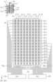
도 9는 일 실시예에 따른 터치 디바이스 상에 스타일러스 펜이 위치한 경우를 나타낸 도면이다.9 is a diagram illustrating a case where a stylus pen is positioned on a touch device according to an embodiment.
도 9에 도시된 바와 같이, 스타일러스 펜(10a, 10b)의 인덕터부(14)는 터치 스크린(20) 상에서, 제1 터치 전극들(111-5, 111-6) 사이, 제2 터치 전극들(121-8, 121-9) 사이에 위치한다.As shown in FIG. 9 , the
스타일러스 펜(10a, 10b)은 안테나(121A) 또는 두 개의 신호 입력단을 갖는 터치 전극(111, 121)에 인가된 구동 신호에 의해 공진한다. 공진에 의해 인덕터부(14)의 코일에 흐르는 전류(Ir)가 흐른다. 이러한 전류(Ir)는 터치 전극들(111, 121)과 트레이스들(112, 122a, 122b)에 와전류(eddy current)를 야기한다. 이러한 와전류는 전류(Ir) 방향의 반대 방향으로 형성된다.The stylus pens 10a and 10b resonate by driving signals applied to the
그러므로, 인덕터부(14)의 좌측(-X축 방향)에 위치한 제1 터치 전극들(111-4, 111-5)에는 -Y축 방향으로 전류(Ia1, Ia2)가 형성되고, 인덕터부(14)의 우측(+X축 방향)에 위치한 제1 터치 전극들(111-6, 111-7)에는 +Y축 방향으로 전류(Ia3, Ia4)가 형성된다. 즉, 제1 터치 전극들(111-1 내지 111-5)에 유도되는 전류의 방향과 제1 터치 전극들(111-6 내지 111-10)에 유도되는 전류의 방향이 서로 반대이다.Therefore, currents Ia1 and Ia2 are formed in the -Y axis direction in the first touch electrodes 111-4 and 111-5 located on the left side (-X axis direction) of the
인덕터부(14)의 상측(+Y축 방향)에 위치한 제2 터치 전극들(121-7, 121-8)에는 -X축 방향으로 전류(Ib1, Ib2)가 형성되고, 인덕터부(14)의 하측(-Y축 방향)에 위치한 제2 터치 전극들(121-9, 121-10)에는 +X축 방향으로 전류(Ib3, Ib4)가 형성된다. 즉, 제2 터치 전극들(121-1 내지 121-8)에 유도되는 전류의 방향과 제2 터치 전극들(121-9 내지 121-16)에 유도되는 전류의 방향이 서로 반대이다.Currents Ib1 and Ib2 are formed in the -X-axis direction in the second touch electrodes 121-7 and 121-8 located on the upper side (+Y-axis direction) of the
인덕터부(14)의 좌측에 위치한 트레이스들(122a)에는 -Y축 방향으로 전류(Ic1, Ic2)가 형성되고, 인덕터부(14)의 우측에 위치한 트레이스들(122b)에는 +Y축 방향으로 전류(Ic3, Ic4)가 형성된다. 즉, 트레이스들(122a)에 유도되는 전류의 방향과 트레이스들(122b)에 유도되는 전류의 방향이 서로 반대이다.Currents Ic1 and Ic2 are formed in the -Y-axis direction in the
또한, 제2 터치 전극들(121-1 내지 121-8)에 유도되는 전류의 방향과 제2 터치 전극들(121-1 내지 121-8)에 연결된 트레이스들(122a)에 유도되는 전류의 방향은 동일하다. 제2 터치 전극들(121-9 내지 121-16)에 유도되는 전류의 방향과 제2 터치 전극들(121-9 내지 121-16)에 연결된 트레이스들(122b)에 유도되는 전류의 방향은 서로 반대이다.Also, the direction of the current induced in the second touch electrodes 121-1 to 121-8 and the direction of the current induced in the
한 시점에서 전류의 방향을, 패드(113a, 113b)를 기준으로 살펴보면, 제2 터치 전극들(121-1 내지 121-8)로부터 패드(113a)로 전류가 인입될 수 있다. 제2 터치 전극들(121-9 내지 121-16)과 이에 연결된 트레이스들(122b)에 유도되는 전류의 크기에 따라 패드(113b)로부터 제2 터치 전극들(121-9 내지 121-16)로 인출되거나, 제2 터치 전극들(121-9 내지 121-16)로부터 패드(113b)로 전류가 인입될 수 있다. 다만, 도 9에서는 스타일러스 펜(10)의 인덕터부(14)가 트레이스들(122b)에 비해 제2 터치 전극들(121-9 내지 121-16)에 더 가깝게 위치하므로, 제2 터치 전극들(121-9 내지 121-16)로부터 패드(113b)에 전류가 인입될 수 있다.Looking at the direction of the current at a point in time with respect to the
이와는 별개로, 도 5의 (b)의 스타일러스 펜(10b)의 경우, 전기장 신호(E)를 터치 전극들(111, 121)에 출력하므로, 제1 터치 전극들(111-5, 111-6)과 제2 터치 전극들(121-8, 121-9)에 인가되는 전기장 신호(E)에 의한 감지 신호가 수신된다.Apart from this, in the case of the
관련하여, 도 10을 참조하여 신호 측정 방법에 대해 설명한다.In this regard, a method for measuring a signal will be described with reference to FIG. 10 .
도 10은 실시예들에 따른 터치 디바이스의 신호 측정 방법을 나타낸 그래프이다.10 is a graph illustrating a method for measuring a signal of a touch device according to embodiments.
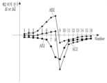
도 10은 서로 반대 방향의 전류가 유도되는 제2 터치 전극(121-8)의 전압 변화(V8)와 제2 터치 전극(121-9)의 전압 변화(V9)를 나타낸다.10 shows a voltage change (V8) of the second touch electrode 121-8 and a voltage change (V9) of the second touch electrode 121-9, in which currents in opposite directions are induced.
제1 구동/수신부(2620)와 제2 구동/수신부(2622)는 전압 변화에 따른 감지 신호를 측정하기 위해, 구동 신호의 주파수에 대응하여 전압 변화를 샘플링한다. 적어도 하나의 샘플링 시점(I, Q, IB, QB)은, 구동 신호의 주파수와 관련되어 주기적으로 설정될 수 있는 임의의 타이밍일 수 있다. 예를 들어, I와 I 사이의 기간은 구동 신호의 반 주기와 동일하다.The first driving/
감지 신호는 I 시점에서 측정한 전압 값과 IB 시점에서 측정한 전압 값의 차(ΔI) 및/또는 Q 시점에서 측정한 전압 값과 QB 시점에서 측정한 전압 값의 차(ΔQ)를 포함한다.The detection signal includes a difference (ΔI) between a voltage value measured at time I and a voltage value measured at time IB and/or a difference (ΔQ) between a voltage value measured at time Q and a voltage value measured at time QB.
다음으로 도 11 및 도 12를 참조하여, 도 5의 (b)의 스타일러스 펜(10b)에 의한 감지 신호에 대해 설명한다.Next, with reference to FIGS. 11 and 12, the detection signal by the
도 11 및 도 12는 일 실시예에 따른 스타일러스 펜에 의한 감지 신호를 나타낸 그래프이다.11 and 12 are graphs showing detection signals by a stylus pen according to an embodiment.
도 11은 제1 터치 전극들(111-1 내지 111-10)로부터 수신한 감지 신호의 그래프이다.11 is a graph of detection signals received from the first touch electrodes 111-1 to 111-10.
도 11에 도시된 바와 같이, 제1 터치 전극들(111-1 내지 111-5)과 제1 터치 전극들(111-6 내지 111-10) 사이의 전류 방향은 반대로 유도되므로, 이에 의해 측정된 감지 신호(AB1)는 제1 터치 전극(111-5)과 제1 터치 전극(111-6)에서 반대의 부호를 갖는다. 또한, 인덕터부(14)와 가까울수록 더 큰 전류가 유도될 것이므로, 제1 터치 전극(111-5)과 제1 터치 전극(111-6)에 유도된 전류의 크기는 다른 제1 터치 전극들(111-1 내지 111-4, 111-7 내지 111-10)에 유도된 전류의 크기보다 더 크다.As shown in FIG. 11, since the direction of current between the first touch electrodes 111-1 to 111-5 and the first touch electrodes 111-6 to 111-10 is induced in the opposite direction, the measured The detection signal AB1 has an opposite sign between the first touch electrode 111-5 and the first touch electrode 111-6. In addition, since a larger current is induced as it is closer to the
스타일러스 펜(10b)은 도전성 팁(11b)을 통해 전기장 신호(E)를 제1 터치 전극(111-5)과 제1 터치 전극(111-6)에 출력하므로, 이에 의한 감지 신호(AE1)가 수신된다.Since the
제1 구동/수신부(2620)에 의해 수신되는 감지 신호(AC1)는 감지 신호(AB1)와 감지 신호(AE1)가 결합된 형태를 갖는다. 이 경우 제어부(2624)는 감지 신호(AC1)의 크기 차이가 최대인 두 제1 터치 전극(111-5, 111-6) 사이를 터치 지점으로 결정할 수 있고, 정확한 터치 지점은 보간 등을 사용하여 계산될 수 있다.The detection signal AC1 received by the first driving/
도 12는 제2 터치 전극들(121-1 내지 121-16)로부터 수신한 감지 신호의 그래프이다.12 is a graph of detection signals received from the second touch electrodes 121-1 to 121-16.
도 12에 도시된 바와 같이, 제2 터치 전극들(121-1 내지 121-8)과 제2 터치 전극들(121-9 내지 121-16) 사이의 전류 방향은 반대로 유도되므로, 이에 의해 측정된 감지 신호(AB2)는 제2 터치 전극(121-8)과 제2 터치 전극(121-9)에서 반대의 부호를 갖는다. 또한, 인덕터부(14)와 가까울수록 더 큰 전류가 유도될 것이므로, 제2 터치 전극(121-8)과 제2 터치 전극(121-9)에 유도된 전류의 크기는 다른 제2 터치 전극들(121-1 내지 121-7, 121-10 내지 121-16)에 유도된 전류의 크기보다 더 크다.As shown in FIG. 12, since the direction of the current between the second touch electrodes 121-1 to 121-8 and the second touch electrodes 121-9 to 121-16 is reversed, the measured The detection signal AB2 has an opposite sign between the second touch electrode 121-8 and the second touch electrode 121-9. In addition, since a larger current is induced as it is closer to the
스타일러스 펜(10b)은 도전성 팁(11b)을 통해 전기장 신호(E)를 제2 터치 전극(121-8)과 제2 터치 전극(121-9)에 출력하므로, 이에 의한 감지 신호(AE2)가 수신된다.Since the
제2 구동/수신부(2622)에 의해 수신되는 감지 신호(AC2)는 감지 신호(AB2)와 감지 신호(AE2)가 결합된 형태를 갖는다. 이 경우 제어부(2624)는 감지 신호(AC2)의 크기 차이가 최대인 두 제2 터치 전극(121-8, 121-9) 사이를 터치 지점으로 결정할 수 있고, 정확한 터치 지점은 보간 등을 사용하여 계산될 수 있다.The detection signal AC2 received by the second driving/
다음으로 도 13 및 도 14를 참조하여, 도 5의 (a)의 스타일러스 펜(10a)에 의한 감지 신호에 대해 설명한다.Next, with reference to FIGS. 13 and 14, the detection signal by the
도 13 및 도 14는 다른 실시예에 따른 스타일러스 펜에 의한 감지 신호를 나타낸 그래프이다.13 and 14 are graphs showing detection signals by a stylus pen according to another embodiment.
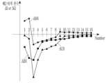
도 13은 제1 터치 전극들(111-1 내지 111-10)로부터 수신한 감지 신호의 그래프이다.13 is a graph of detection signals received from the first touch electrodes 111-1 to 111-10.
도 13에 도시된 바와 같이, 제1 터치 전극들(111-1 내지 111-5)과 제1 터치 전극들(111-6 내지 111-10) 사이의 전류 방향은 반대로 유도되므로, 제1 구동/수신부(2620)에 의해 수신되는 감지 신호(AB3)는 제1 터치 전극(111-5)과 제1 터치 전극(111-6)에서 반대의 부호를 갖는다. 또한, 인덕터부(14)와 가까울수록 더 큰 전류가 유도될 것이므로, 제1 터치 전극(111-5)과 제1 터치 전극(111-6)에 유도된 전류의 크기는 다른 제1 터치 전극들(111-1 내지 111-4, 111-7 내지 111-10)에 유도된 전류의 크기보다 더 크다.As shown in FIG. 13 , since the direction of the current between the first touch electrodes 111-1 to 111-5 and the first touch electrodes 111-6 to 111-10 is reversed, the first driving / The detection signal AB3 received by the
이 경우 제어부(2624)는 감지 신호(AB3)의 부호가 반대되면서 각각의 신호 크기가 큰 두 제1 터치 전극(111-5, 111-6) 사이를 터치 지점으로 결정할 수 있고, 정확한 터치 지점은 보간 등을 사용하여 계산될 수 있다. 이 경우 제어부(2624)는 감지 신호(AB3)를 미분하여 최댓값을 갖는 영역을 터치 지점으로 결정할 수 있다.In this case, the
도 14는 제2 터치 전극들(121-1 내지 121-16)로부터 수신한 감지 신호의 그래프이다.14 is a graph of detection signals received from the second touch electrodes 121-1 to 121-16.
도 14에 도시된 바와 같이, 제2 터치 전극들(121-1 내지 121-8)과 제2 터치 전극들(121-9 내지 121-16) 사이의 전류 방향은 반대로 유도되므로, 제2 구동/수신부(2622)에 의해 수신되는 감지 신호(AB4)는 제2 터치 전극(121-8)과 제2 터치 전극(121-9)에서 반대의 부호를 갖는다. 또한, 인덕터부(14)와 가까울수록 더 큰 전류가 유도될 것이므로, 제2 터치 전극(121-8)과 제2 터치 전극(121-9)에 유도된 전류의 크기는 다른 제2 터치 전극들(121-1 내지 121-7, 121-10 내지 121-16)에 유도된 전류의 크기보다 더 크다.As shown in FIG. 14, since the direction of current between the second touch electrodes 121-1 to 121-8 and the second touch electrodes 121-9 to 121-16 is reversed, the second drive/ The detection signal AB4 received by the
이 경우 제어부(2624)는 감지 신호(AB4)의 부호가 반대되면서 각각의 신호 크기가 큰 두 제2 터치 전극(121-8, 121-9) 사이를 터치 지점으로 결정할 수 있고, 정확한 터치 지점은 보간 등을 사용하여 계산될 수 있다.In this case, the
다음으로, 도 15를 참조하여 터치 스크린(20) 상에 스타일러스 펜(10a 또는 10b)이 위치한 경우, 터치 전극(111, 121)과 트레이스(112, 122a, 122b)에 유도되는 신호에 대해 설명한다.Next, referring to FIG. 15, when the
도 15는 일 실시예에 따른 터치 디바이스 상에 스타일러스 펜이 위치한 경우를 나타낸 도면이다.15 is a diagram illustrating a case where a stylus pen is positioned on a touch device according to an embodiment.
도 15에 도시된 바와 같이, 스타일러스 펜(10a, 10b)의 인덕터부(14)는 터치 스크린(20) 상에서, 제1 터치 전극들(111-2, 111-3) 사이, 제2 터치 전극들(121-2, 121-3) 사이에 위치한다.As shown in FIG. 15 , the
스타일러스 펜(10a, 10b)은 안테나(121A) 또는 두 개의 신호 입력단을 갖는 터치 전극(111, 121)에 인가된 구동 신호에 의해 공진한다. 공진에 의해 인덕터부(14)의 코일에 흐르는 전류(Ir)가 흐른다. 이러한 전류(Ir)는 터치 전극들(111, 121)과 트레이스들(112, 122a, 122b)에 와전류(eddy current)를 야기한다. 이러한 와전류는 전류(Ir) 방향의 반대 방향으로 형성된다.The stylus pens 10a and 10b resonate by driving signals applied to the
그러므로, 인덕터부(14)의 좌측(-X축 방향)에 위치한 제1 터치 전극들(111-1, 111-2)에는 -Y축 방향으로 전류(Ia1, Ia2)가 형성되고, 인덕터부(14)의 우측(+X축 방향)에 위치한 제1 터치 전극들(111-3, 111-4)에는 +Y축 방향으로 전류(Ia3, Ia4)가 형성된다. 즉, 제1 터치 전극들(111-1 및 111-2)에 유도되는 전류의 방향과 제1 터치 전극들(111-3 내지 111-10)에 유도되는 전류의 방향이 서로 반대이다.Therefore, currents Ia1 and Ia2 are formed in the -Y axis direction in the first touch electrodes 111-1 and 111-2 located on the left side (-X axis direction) of the
인덕터부(14)의 상측(+Y축 방향)에 위치한 제2 터치 전극들(121-1, 121-2)에는 -X축 방향으로 전류(Ib1, Ib2)가 형성되고, 인덕터부(14)의 하측(-Y축 방향)에 위치한 제2 터치 전극들(121-3, 121-4, 121-9, 121-10)에는 +X축 방향으로 전류(Ib3, Ib4, Ib5, Ib6)가 형성된다. 즉, 제2 터치 전극들(121-1 및 121-2)에 유도되는 전류의 방향과 제2 터치 전극들(121-3 내지 121-16)에 유도되는 전류의 방향이 서로 반대이다.Currents Ib1 and Ib2 are formed in the -X-axis direction in the second touch electrodes 121-1 and 121-2 located on the upper side (+Y-axis direction) of the
인덕터부(14)의 좌측에 위치한 트레이스들(122a)에는 -Y축 방향으로 전류(Ic1 내지 Ic4)가 형성되고, 인덕터부(14)의 우측에 위치한 트레이스들(122b)에는 +Y축 방향으로 전류(Ic5, Ic6)가 형성된다. 즉, 트레이스들(122a)에 유도되는 전류의 방향과 트레이스들(122b)에 유도되는 전류의 방향이 서로 반대이다.Currents Ic1 to Ic4 are formed in the -Y-axis direction in the
또한, 제2 터치 전극들(121-1 및 121-2)에 유도되는 전류의 방향과 제2 터치 전극들(121-1 및 121-2)에 연결된 트레이스들(122a)에 유도되는 전류의 방향은 동일하다. 제2 터치 전극들(121-3 내지 121-8)에 유도되는 전류의 방향과 제2 터치 전극들(121-3 내지 121-8)에 연결된 트레이스들(122a)에 유도되는 전류의 방향은 서로 반대이다. 제2 터치 전극들(121-9 내지 121-16)에 유도되는 전류의 방향과 제2 터치 전극들(121-9 내지 121-16)에 연결된 트레이스들(122b)에 유도되는 전류의 방향은 서로 반대이다.Also, the direction of the current induced in the second touch electrodes 121-1 and 121-2 and the direction of the current induced in the
한 시점에서 전류의 방향을, 패드(113a, 113b)를 기준으로 살펴보면, 제2 터치 전극들(121-1 및 121-2)로부터 패드(113a)로 전류가 인입될 수 있다. 제2 터치 전극들(121-3 내지 121-16)과 이에 연결된 트레이스들(122a, 122b)에 유도되는 전류의 크기에 따라 패드(113a, 113b)로부터 제2 터치 전극들(121-3 내지 121-16)로 인출되거나, 제2 터치 전극들(121-3 내지 121-16)로부터 패드(113a, 113b)로 전류가 인입될 수 있다.Looking at the direction of the current at a point in time with respect to the
이와는 별개로, 도 5의 (b)의 스타일러스 펜(10b)의 경우, 전기장 신호(E)를 터치 전극들(111, 121)에 출력하므로, 제1 터치 전극들(111-2, 111-3)과 제2 터치 전극들(121-2, 121-3)에 인가되는 전기장 신호(E)에 의한 감지 신호가 수신된다.Apart from this, in the case of the
다음으로 도 16 및 도 17을 참조하여, 도 5의 (b)의 스타일러스 펜(10b)에 의한 감지 신호에 대해 설명한다.Next, with reference to FIGS. 16 and 17, the detection signal by the
도 16 및 도 17은 일 실시예에 따른 스타일러스 펜에 의한 감지 신호를 나타낸 그래프이다.16 and 17 are graphs showing detection signals by a stylus pen according to an embodiment.
도 16에 도시된 바와 같이, 제1 터치 전극들(111-1 및 111-2)과 제1 터치 전극들(111-3 내지 111-10) 사이의 전류 방향은 반대로 유도되므로, 이에 의해 측정된 감지 신호(AB5)는 제1 터치 전극(111-2)과 제1 터치 전극(111-3)에서 반대의 부호를 갖는다. 또한, 인덕터부(14)와 가까울수록 더 큰 전류가 유도될 것이므로, 제1 터치 전극(111-2)과 제1 터치 전극(111-3)에 유도된 전류의 크기는 다른 제1 터치 전극들(111-1, 111-4 내지 111-10)에 유도된 전류의 크기보다 더 크다.As shown in FIG. 16, since the direction of the current between the first touch electrodes 111-1 and 111-2 and the first touch electrodes 111-3 to 111-10 is induced in the opposite direction, the measured The detection signal AB5 has an opposite sign between the first touch electrode 111-2 and the first touch electrode 111-3. In addition, since a larger current is induced as it is closer to the
스타일러스 펜(10b)은 도전성 팁(11b)을 통해 전기장 신호(E)를 제1 터치 전극(111-2)과 제1 터치 전극(111-3)에 출력하므로, 이에 의한 감지 신호(AE5)가 수신된다.Since the
제1 구동/수신부(2620)에 의해 수신되는 감지 신호(AC5)는 감지 신호(AB5)와 감지 신호(AE5)가 결합된 형태를 갖는다. 이 경우 제어부(2624)는 감지 신호(AC5)의 크기 차이가 최대인 두 제1 터치 전극(111-2, 111-3) 사이를 터치 지점으로 결정할 수 있고, 정확한 터치 지점은 보간 등을 사용하여 계산될 수 있다.The detection signal AC5 received by the first driving/
도 17은 제2 터치 전극들(121-1 내지 121-16)로부터 수신한 감지 신호의 그래프이다.17 is a graph of detection signals received from the second touch electrodes 121-1 to 121-16.
도 17에 도시된 바와 같이, 제2 터치 전극들(121-1 및 121-2)과 제2 터치 전극들(121-3 내지 121-16) 사이의 전류 방향은 반대로 유도되므로, 이에 의해 측정된 감지 신호(AB6)는 제2 터치 전극(121-2)과 제2 터치 전극(121-3)에서 반대의 부호를 갖는다. 또한, 인덕터부(14)와 가까울수록 더 큰 전류가 유도될 것이므로, 제2 터치 전극(121-2)과 제2 터치 전극(121-3)에 유도된 전류의 크기는 다른 제2 터치 전극들(121-1, 121-4 내지 121-16)에 유도된 전류의 크기보다 더 크다.As shown in FIG. 17, since the direction of the current between the second touch electrodes 121-1 and 121-2 and the second touch electrodes 121-3 to 121-16 is reversed, the measured The detection signal AB6 has an opposite sign between the second touch electrode 121-2 and the second touch electrode 121-3. In addition, since a larger current is induced closer to the
스타일러스 펜(10b)은 도전성 팁(11b)을 통해 전기장 신호(E)를 제2 터치 전극(121-2)과 제2 터치 전극(121-3)에 출력하므로, 이에 의한 감지 신호(AE6)가 수신된다.Since the
제2 구동/수신부(2622)에 의해 수신되는 감지 신호(AC6)는 감지 신호(AB6)와 감지 신호(AE6)가 결합된 형태를 갖는다. 이 경우 제어부(2624)는 감지 신호(AC6)의 크기 차이가 최대인 두 제2 터치 전극(121-2, 121-3) 사이를 터치 지점으로 결정할 수 있고, 정확한 터치 지점은 보간 등을 사용하여 계산될 수 있다.The detection signal AC6 received by the second driving/
다음으로 도 18 및 도 19를 참조하여, 도 5의 (a)의 스타일러스 펜(10a)에 의한 감지 신호에 대해 설명한다.Next, with reference to FIGS. 18 and 19, the detection signal by the
도 18 및 도 19는 다른 실시예에 따른 스타일러스 펜에 의한 감지 신호를 나타낸 그래프이다.18 and 19 are graphs showing detection signals by a stylus pen according to another embodiment.
도 18은 제1 터치 전극들(111-1 내지 111-10)로부터 수신한 감지 신호의 그래프이다.18 is a graph of detection signals received from the first touch electrodes 111-1 to 111-10.
도 18에 도시된 바와 같이, 제1 터치 전극들(111-1 및 111-2)과 제1 터치 전극들(111-3 내지 111-10) 사이의 전류 방향은 반대로 유도되므로, 제1 구동/수신부(2620)에 의해 수신되는 감지 신호(AB7)는 제1 터치 전극(111-2)과 제1 터치 전극(111-3)에서 반대의 부호를 갖는다. 또한, 인덕터부(14)와 가까울수록 더 큰 전류가 유도될 것이므로, 제1 터치 전극(111-2)과 제1 터치 전극(111-3)에 유도된 전류의 크기는 다른 제1 터치 전극들(111-1, 111-4 내지 111-10)에 유도된 전류의 크기보다 더 크다.As shown in FIG. 18, since the direction of the current between the first touch electrodes 111-1 and 111-2 and the first touch electrodes 111-3 to 111-10 is reversed, the first driving / The detection signal AB7 received by the
이 경우 제어부(2624)는 감지 신호(AB7)의 부호가 반대되면서 각각의 신호 크기가 큰 두 제1 터치 전극(111-2, 111-3) 사이를 터치 지점으로 결정할 수 있고, 정확한 터치 지점은 보간 등을 사용하여 계산될 수 있다.In this case, the
도 19는 제2 터치 전극들(121-1 내지 121-16)로부터 수신한 감지 신호의 그래프이다.19 is a graph of detection signals received from the second touch electrodes 121-1 to 121-16.
도 19에 도시된 바와 같이, 제2 터치 전극들(121-1 및 121-2)과 제2 터치 전극들(121-3 내지 121-16) 사이의 전류 방향은 반대로 유도되므로, 제2 구동/수신부(2622)에 의해 수신되는 감지 신호(AB8)는 제2 터치 전극(121-2)과 제2 터치 전극(121-3)에서 반대의 부호를 갖는다. 또한, 인덕터부(14)와 가까울수록 더 큰 전류가 유도될 것이므로, 제2 터치 전극(121-2)과 제2 터치 전극(121-3)에 유도된 전류의 크기는 다른 제2 터치 전극들(121-1, 121-4내지 121-16)에 유도된 전류의 크기보다 더 크다.As shown in FIG. 19, since the direction of current between the second touch electrodes 121-1 and 121-2 and the second touch electrodes 121-3 to 121-16 is reversed, the second drive/ The detection signal AB8 received by the
이 경우 제어부(2624)는 감지 신호(AB8)의 부호가 반대되면서 각각의 신호 크기가 큰 두 제2 터치 전극(121-2, 121-3) 사이를 터치 지점으로 결정할 수 있고, 정확한 터치 지점은 보간 등을 사용하여 계산될 수 있다.In this case, the
다음으로 도 20을 참조하여, 도 2의 (c)의 터치 스크린(20c)를 갖는 전자 디바이스(2)에 대해 설명한다.Next, referring to FIG. 20, the
도 20은 전자 디바이스를 개략적으로 나타낸 블록도이다.20 is a schematic block diagram of an electronic device.
도 20의 전자 디바이스는 도 4의 전자 디바이스에 비해, 루프 코일(264)과 루프 코일(264)에 구동 신호를 인가하는 코일 드라이버(263)를 더 포함한다.Compared to the electronic device of FIG. 4 , the electronic device of FIG. 20 further includes a
루프 코일(264)은 터치 스크린(20)의 근방에 배치될 수 있거나, 전자 디바이스(2) 내의 임의의 위치에 배치될 수도 있다. 루프 코일(264)은 RFID, NFC와 같은 근거리 통신 모듈(212)의 안테나로도 구성될 수 있다. 구동 신호는 소정 주파수를 갖는 교류 전압 또는 교류 전류를 포함한다.The
도 21은 일 실시예에 따른 터치 디바이스의 일부를 개략적으로 나타낸 도면이다.21 is a diagram schematically illustrating a part of a touch device according to an exemplary embodiment.
도 21의 터치 디바이스는 도 6의 터치 디바이스에 비해, 루프 코일(264), 루프 코일(264)을 구동하는 코일 드라이버(263)를 더 포함한다.Compared to the touch device of FIG. 6 , the touch device of FIG. 21 further includes a
코일 드라이버(263)는 루프 코일(264)에 구동 신호를 인가한다. 구동 신호는, 공진 회로부(12)의 공진 주파수에 대응하는 주파수를 갖는 신호(예를 들어, 사인파, 구형파 등)를 포함할 수 있으며, 소정 주파수를 갖는 교류 전압 또는 교류 전류일 수 있다. 이러한 구동 신호의 주파수와 크기는 제어부(2624)의 제어에 따라 변경될 수 있다.The
스타일러스 펜(10a, 10b)은 루프 코일(264)에 인가된 구동 신호에 의해 공진한다. 공진에 의해 인덕터부(14)의 코일에 흐르는 전류(Ir)가 흐른다.The stylus pens 10a and 10b resonate with the driving signal applied to the
도 22는 다른 실시예에 따른 터치 디바이스의 전극 및 트레이스의 배치 형태의 일례를 나타낸 도면이다.22 is a diagram illustrating an example of arrangement of electrodes and traces of a touch device according to another embodiment.
터치 센서 내의 터치 전극들(111, 121)은 터치 영역의 가장자리에 위치하는 주변 영역의 트레이스들(112, 122a, 122b)을 통해 패드들(113a, 113b)에 연결되어 있다. 제1 터치 전극들(111-1, 111-2, 111-3, ...)은 각각의 트레이스들(112)에 대응하여 연결되어 있고, 제2 터치 전극들(121-1, 121-2, 121-3, ...)은 각각의 트레이스들(122a, 122b)에 대응하여 연결되어 있다.The
터치 전극들(111, 121)과 트레이스들(112, 122a, 122b)은 동일한 층으로 형성될 수 있다. 터치 전극들(111, 121)과 트레이스들(112, 122a, 122b)은 메탈 메시, 실버 나노 와이어와 같은 높은 투과율, 저 임피던스를 나타내는 도체 재료로 형성될 수 있다. 그러나, 터치 전극들(111, 121)과 트레이스들(112, 122a, 122b)은 상이한 층으로 위치할 수 있으며, ITO, 그래핀으로 제조될 수 있으며, 이에 제한되지 않는다.The
패드들(113a, 113b)은 터치 컨트롤러(262)에 접속되어 있으며, 터치 컨트롤러(262)의 신호(예컨대, 구동 신호)를 터치 전극들(111, 121)에 전달하고, 터치 전극들(111, 121)로부터의 신호(예컨대, 감지 신호)를 터치 컨트롤러(262)에 전달한다.The
도 23은 터치 모듈 및 호스트를 나타내는 블록도이고, 도 24는 터치 모듈로부터 호스트에 제공되는 터치 데이터의 일 예를 나타내는 도면이다.23 is a block diagram illustrating a touch module and a host, and FIG. 24 is a diagram illustrating an example of touch data provided from a touch module to a host.
도 23을 참조하면, 호스트(270)는 터치 모듈(260)에 포함된 터치 컨트롤러(262)에 터치 데이터를 제공받을 수 있다. 예를 들어, 호스트(270)는 모바일 SoC(System-on-Chip), 어플리케이션 프로세서(AP: Application Processor), 미디어 프로세서(Media Processor), 마이크로프로세서, 중앙 처리 장치(CPU: Central Processing Unit), 또는 이와 유사한 장치일 수 있다.Referring to FIG. 23 , the
터치 모듈(260)은 1 프레임이 종료된 후에, 1 프레임 동안 입력된 터치에 관한 정보를 터치 데이터로 생성하여 호스트(270)에 전달할 수 있다.After one frame ends, the
도 23 및 도 24를 참조하면, 터치 데이터(600)는 터치 모듈(260)로부터 호스트(270)로 전달될 수 있고, 터치 카운트 필드(610) 및 적어도 하나의 터치 엔티티 필드(612, 614)를 포함할 수 있다. 이외에도 터치 데이터(600)에는 스타일러스 펜(10)으로부터의 센서 입력 데이터, 공진 신호 변경을 나타내는 데이터 등이 더 포함될 수 있다.23 and 24 , touch data 600 may be transmitted from the
터치 카운트 필드(610)에는 1 프레임 구간 동안 입력된 터치의 개수를 나타내는 값이 기입될 수 있다. 터치 엔티티 필드(612, 614)는 각각의 터치 입력에 대한 정보를 나타내는 필드를 포함한다. 예를 들어, 터치 엔티티 필드(612, 614)는 플래그 필드(620), X축 좌표 필드(621), Y축 좌표 필드(622), Z 값 필드(623), 면적 필드(624), 터치 액션 필드(625)를 포함한다.A value indicating the number of touches input during one frame period may be written in the touch count field 610 . The touch entity fields 612 and 614 include fields representing information on each touch input. For example, the touch entity fields 612 and 614 include a
터치 엔티티 필드(612, 614)의 개수는 터치 카운트 필드(610)에 기입된 값과 동일할 수 있다.The number of touch entity fields 612 and 614 may be the same as the value written in the touch count field 610 .
플래그 필드(620)에는 터치 객체를 나타내는 값이 기입될 수 있다. 예를 들어, 손가락, 손바닥, 및 스타일러스 펜은 서로 상이한 값으로 플래그 필드(620)에 기입될 수 있다. X축 좌표 필드(621)와 Y축 좌표 필드(622)에는 계산된 터치 좌표를 나타내는 값이 기입될 수 있다. Z 값 필드(623)에는 감지 신호의 신호 세기에 대응되는 값이 기입될 수 있다. 면적 필드(624)에는 터치된 영역의 면적에 대응되는 값이 기입될 수 있다.A value indicating a touch object may be written in the
실시예들에 따르면, 터치 데이터(600)를 전달 받은 호스트(270)는 면적 필드(624)의 값을 사용하여, 터치 면적이 임계치보다 크면 터치 객체가 손가락인 것으로 결정하고, 터치 면적이 임계치 이하이면 터치 객체가 스타일러스 펜(10)인 것으로 결정한다.According to embodiments, the
실시예들에 따르면, 터치 데이터(600)를 전달 받은 호스트(270)는 플래그 필드(620)의 값을 사용하여, 터치 객체가 손가락인지 또는 스타일러스 펜(10)인지를 식별할 수도 있다.According to embodiments, the
본 문서에 개시된 다양한 실시예들에 따른 전자 디바이스는 다양한 형태의 장치가 될 수 있다. 전자 디바이스는, 예를 들면, 휴대용 통신 장치(예: 스마트 폰), 컴퓨터 장치, 휴대용 멀티미디어 장치, 휴대용 의료 기기, 카메라, 웨어러블 장치, 또는 가전 장치를 포함할 수 있다. 본 문서의 실시예에 따른 전자 디바이스는 전술한 기기들에 한정되지 않는다.An electronic device according to various embodiments disclosed in this document may be various types of devices. The electronic device may include, for example, a portable communication device (eg, a smart phone), a computer device, a portable multimedia device, a portable medical device, a camera, a wearable device, or a home appliance. An electronic device according to an embodiment of this document is not limited to the aforementioned devices.
본 문서의 다양한 실시예들 및 이에 사용된 용어들은 본 문서에 기재된 기술적 특징들을 특정한 실시예들로 한정하려는 것이 아니며, 해당 실시예의 다양한 변경, 균등물, 또는 대체물을 포함하는 것으로 이해되어야 한다. 도면의 설명과 관련하여, 유사한 또는 관련된 구성요소에 대해서는 유사한 참조 부호가 사용될 수 있다. 아이템에 대응하는 명사의 단수 형은 관련된 문맥상 명백하게 다르게 지시하지 않는 한, 상기 아이템 한 개 또는 복수 개를 포함할 수 있다. 본 문서에서, "A 또는 B", "A 및 B 중 적어도 하나", "A 또는 B 중 적어도 하나,""A, B 또는 C," "A, B, 및 C 중 적어도 하나,"및 "A, B, 또는 C 중 적어도 하나"와 같은 문구들 각각은 그 문구들 중 해당하는 문구에 함께 나열된 항목들의 모든 가능한 조합을 포함할 수 있다. "제1", "제2", 또는 "첫째" 또는 "둘째"와 같은 용어들은 단순히 해당 구성요소를 다른 해당 구성요소와 구분하기 위해 사용될 수 있으며, 해당 구성요소들을 다른 측면(예: 중요성 또는 순서)에서 한정하지 않는다. 어떤(예: 제1) 구성요소가 다른(예: 제 2) 구성요소에, "기능적으로" 또는 "통신적으로"라는 용어와 함께 또는 이런 용어 없이, "커플드(결합된)" 또는 "커넥티드(연결된)"라고 언급된 경우, 그것은 상기 어떤 구성요소가 상기 다른 구성요소에 직접적으로(예: 유선으로), 무선으로, 또는 제 3 구성요소를 통하여 연결될 수 있다는 것을 의미한다.Various embodiments of this document and terms used therein are not intended to limit the technical features described in this document to specific embodiments, but should be understood to include various modifications, equivalents, or substitutes of the embodiments. In connection with the description of the drawings, like reference numbers may be used for like or related elements. The singular form of a noun corresponding to an item may include one item or a plurality of items, unless the relevant context clearly dictates otherwise. In this document, "A or B", "at least one of A and B", "at least one of A or B," "A, B or C," "at least one of A, B, and C," and " Each of the phrases such as "at least one of A, B, or C" may include all possible combinations of the items listed together in the corresponding one of the phrases. Terms such as "first", "second", or "first" or "secondary" may simply be used to distinguish that component from other corresponding components, and may refer to that component in other respects (eg, importance or order) is not limited. A (e.g. first) component is “coupled” or “coupled” to another (e.g. second) component, with or without the terms “functionally” or “communicatively”. When it says connected (connected), it means that the certain component can be connected to the other component directly (eg, by wire), wirelessly, or through a third component.
본 문서에서 사용된 용어 "모듈"은 하드웨어, 소프트웨어 또는 펌웨어로 구현된 유닛을 포함할 수 있으며, 예를 들면, 로직, 논리 블록, 부품, 또는 회로 등의 용어와 상호 호환적으로 사용될 수 있다. 모듈은, 일체로 구성된 부품 또는 하나 또는 그 이상의 기능을 수행하는, 상기 부품의 최소 단위 또는 그 일부가 될 수 있다. 예를 들면, 일 실시예에 따르면, 모듈은 ASIC(application-specific integrated circuit)의 형태로 구현될 수 있다.The term "module" used in this document may include a unit implemented by hardware, software, or firmware, and may be used interchangeably with terms such as logic, logic block, component, or circuit, for example. A module may be an integrally constructed component or a minimal unit of components or a portion thereof that performs one or more functions. For example, according to one embodiment, the module may be implemented in the form of an application-specific integrated circuit (ASIC).
본 문서의 다양한 실시예들은 기기(machine)(예: 전자 디바이스) 의해 읽을 수 있는 저장 매체(Storage medium)(예: 내장 메모리 또는 외장 메모리)에 저장된 하나 이상의 명령어들을 포함하는 소프트웨어(예: 프로그램)로서 구현될 수 있다. 예를 들면, 기기(예: 전자 디바이스)의 프로세서(예: 프로세서)는, 저장 매체로부터 저장된 하나 이상의 명령어들 중 적어도 하나의 명령을 호출하고, 그것을 실행할 수 있다. 이것은 기기가 상기 호출된 적어도 하나의 명령어에 따라 적어도 하나의 기능을 수행하도록 운영되는 것을 가능하게 한다. 상기 하나 이상의 명령어들은 컴파일러에 의해 생성된 코드 또는 인터프리터에 의해 실행될 수 있는 코드를 포함할 수 있다. 기기로 읽을 수 있는 저장매체 는, 비일시적(non-transitory) 저장매체의 형태로 제공될 수 있다. 여기서, '비일시적'은 저장매체가 실재(tangible)하는 장치이고, 신호(Signal)(예: 전자기파)를 포함하지 않는다는 것을 의미할 뿐이며, 이 용어는 데이터가 저장매체에 반영구적으로 저장되는 경우와 임시적으로 저장되는 경우를 구분하지 않는다.Various embodiments of this document are software (eg, a program) including one or more instructions stored in a storage medium (eg, internal memory or external memory) readable by a machine (eg, an electronic device). can be implemented as For example, a processor (eg, a processor) of a device (eg, an electronic device) may call at least one command among one or more instructions stored from a storage medium and execute it. This enables the device to be operated to perform at least one function according to the at least one command invoked. The one or more instructions may include code generated by a compiler or code executable by an interpreter. Device-readable storage media may be provided in the form of non-transitory storage media. Here, 'non-temporary' only means that the storage medium is a tangible device and does not contain signals (e.g., electromagnetic waves), and this term refers to the case where data is stored semi-permanently in the storage medium. It does not discriminate when it is temporarily stored.
일 실시예에 따르면, 본 문서에 개시된 다양한 실시예들에 따른 방법은 컴퓨터 프로그램 제품(computer program product)에 포함되어 제공될 수 있다. 컴퓨터 프로그램 제품은 상품으로서 판매자 및 구매자 간에 거래될 수 있다. 컴퓨터 프로그램 제품은 기기로 읽을 수 있는 저장 매체(예: compact disc read only memory (CD-ROM))의 형태로 배포되거나, 또는 어플리케이션 스토어(예: 플레이 스토어??)를 통해 또는 두 개의 사용자 장치들(예: 스마트 폰들) 간에 직접, 온라인으로 배포(예: 다운로드 또는 업로드)될 수 있다. 온라인 배포의 경우에, 컴퓨터 프로그램 제품의 적어도 일부는 제조사의 서버, 어플리케이션 스토어의 서버, 또는 중계 서버의 메모리와 같은 기기로 읽을 수 있는 저장 매체에 적어도 일시 저장되거나, 임시적으로 생성될 수 있다.According to one embodiment, the method according to various embodiments disclosed in this document may be provided by being included in a computer program product. Computer program products may be traded between sellers and buyers as commodities. A computer program product is distributed in the form of a device-readable storage medium (eg compact disc read only memory (CD-ROM)), or through an application store (eg Play Store??) or on two user devices. It can be distributed (eg downloaded or uploaded) online, directly between (eg smart phones). In the case of online distribution, at least part of the computer program product may be temporarily stored or temporarily created in a device-readable storage medium such as a manufacturer's server, an application store server, or a relay server's memory.
다양한 실시예들에 따르면, 상기 기술한 구성요소들의 각각의 구성요소(예: 모듈 또는 프로그램)는 단수 또는 복수의 개체를 포함할 수 있다. 다양한 실시예들에 따르면, 전술한 해당 구성요소들 중 하나 이상의 구성요소들 또는 동작들이 생략되거나, 또는 하나 이상의 다른 구성요소들 또는 동작들이 추가될 수 있다. 대체적으로 또는 추가적으로, 복수의 구성요소들(예: 모듈 또는 프로그램)은 하나의 구성요소로 통합될 수 있다. 이런 경우, 통합된 구성요소는 상기 복수의 구성요소들 각각의 구성요소의 하나 이상의 기능들을 상기 통합 이전에 상기 복수의 구성요소들 중 해당 구성요소에 의해 수행되는 것과 동일 또는 유사하게 수행할 수 있다. 다양한 실시예들에 따르면, 모듈, 프로그램 또는 다른 구성요소에 의해 수행되는 동작들은 순차적으로, 병렬적으로, 반복적으로, 또는 휴리스틱하게 실행되거나, 상기 동작들 중 하나 이상이 다른 순서로 실행되거나, 생략되거나, 또는 하나 이상의 다른 동작들이 추가될 수 있다.According to various embodiments, each component (eg, module or program) of the components described above may include a singular entity or a plurality of entities. According to various embodiments, one or more components or operations among the aforementioned corresponding components may be omitted, or one or more other components or operations may be added. Alternatively or additionally, a plurality of components (eg modules or programs) may be integrated into a single component. In this case, the integrated component may perform one or more functions of each of the plurality of components identically or similarly to those performed by a corresponding component of the plurality of components prior to the integration. . According to various embodiments, the actions performed by a module, program, or other component are executed sequentially, in parallel, iteratively, or heuristically, or one or more of the actions are executed in a different order, or omitted. or one or more other actions may be added.
Claims (22)
Translated fromKorean표시 패널,
상기 표시 패널 위에 위치하는 윈도우,
상기 표시 패널과 상기 윈도우 사이의 복수의 전극, 그리고
상기 복수의 전극으로부터 감지 신호를 수신하여 상기 윈도우에 근접한 상기 스타일러스의 위치를 결정하는 터치 컨트롤러
를 포함하고,
상기 복수의 전극은 상기 공진 회로에 의해 상기 복수의 전극에 유도된 전류의 방향이 서로 반대인 전극들을 포함하고,
상기 터치 컨트롤러는 상기 유도된 전류의 방향이 서로 반대인 전극들 사이를 상기 스타일러스의 위치로 결정하는,
터치 디바이스.A touch device for detecting the position of a stylus including a resonance circuit,
display panel,
a window located on the display panel;
a plurality of electrodes between the display panel and the window; and
A touch controller configured to receive detection signals from the plurality of electrodes and determine the position of the stylus close to the window.
including,
The plurality of electrodes include electrodes in which directions of currents induced in the plurality of electrodes by the resonance circuit are opposite to each other,
The touch controller determines the position of the stylus between electrodes in which the direction of the induced current is opposite to each other.
touch device.
상기 복수의 전극 중 일부는 터치 영역에 위치하고,
상기 터치 디바이스는,
상기 터치 영역의 가장자리에 위치하고 상기 복수의 전극에 대응하여 연결되어 있는 복수의 트레이스를 더 포함하고,
상기 복수의 트레이스는 상기 공진 회로에 의해 상기 복수의 트레이스에 유도된 전류의 방향이 서로 반대인 트레이스들을 포함하는,
터치 디바이스.According to claim 1,
Some of the plurality of electrodes are located in the touch area,
The touch device,
Further comprising a plurality of traces located at edges of the touch area and connected to correspond to the plurality of electrodes;
The plurality of traces include traces in which directions of currents induced in the plurality of traces by the resonant circuit are opposite to each other.
touch device.
상기 복수의 전극은 대응하여 연결된 트레이스와 동일한 방향의 전류가 유도되는,
터치 디바이스.According to claim 2,
In the plurality of electrodes, a current is induced in the same direction as the correspondingly connected trace.
touch device.
상기 복수의 전극은 대응하여 연결된 트레이스와 상이한 방향의 전류가 유도되는,
터치 디바이스.According to claim 2,
In the plurality of electrodes, currents are induced in a direction different from that of the correspondingly connected traces.
touch device.
상기 복수의 전극은 제1 방향으로 연장된 복수의 제1 전극을 포함하고,
상기 복수의 트레이스는 상기 제1 방향과 교차하는 제2 방향으로 연장되어 있고, 상기 복수의 제1 전극 중 일부의 제1 전극의 일단에 연결된 제1 트레이스들과 상기 복수의 제1 전극의 다른 일부의 제1 전극의 타단에 연결된 제2 트레이스들을 포함하는,
터치 디바이스.According to claim 2,
The plurality of electrodes include a plurality of first electrodes extending in a first direction,
The plurality of traces extend in a second direction crossing the first direction, and first traces connected to one end of some first electrodes among the plurality of first electrodes and another part of the plurality of first electrodes. Including second traces connected to the other end of the first electrode of
touch device.
상기 복수의 전극과 동일한 층에 형성된 복수의 더미 전극 및 상기 복수의 더미 전극을 서로 연결하는 복수의 브릿지를 포함하는 안테나를 더 포함하고,
상기 터치 컨트롤러는 상기 안테나에 구동 신호를 인가하여 상기 공진 회로를 감지시키는 자기 신호를 출력하는,
터치 디바이스.According to claim 1,
An antenna including a plurality of dummy electrodes formed on the same layer as the plurality of electrodes and a plurality of bridges connecting the plurality of dummy electrodes to each other;
The touch controller outputs a magnetic signal for sensing the resonance circuit by applying a driving signal to the antenna.
touch device.
상기 복수의 전극 각각은 두 개의 신호 입력단을 포함하고,
상기 터치 컨트롤러는 상기 두 개의 신호 입력단 중 하나는 접지하고, 다른 하나에는 구동 신호를 인가하여 상기 공진 회로를 감지시키는 자기 신호를 출력하는,
터치 디바이스.According to claim 1,
Each of the plurality of electrodes includes two signal input terminals,
The touch controller outputs a magnetic signal for sensing the resonance circuit by grounding one of the two signal input terminals and applying a driving signal to the other.
touch device.
상기 복수의 전극 각각은 두 개의 신호 입력단을 포함하고,
상기 터치 컨트롤러는 상기 두 개의 신호 입력단에 서로 반대 위상의 구동 신호를 인가하여 상기 공진 회로를 감지시키는 자기 신호를 출력하는,
터치 디바이스.According to claim 1,
Each of the plurality of electrodes includes two signal input terminals,
The touch controller outputs a magnetic signal for sensing the resonance circuit by applying driving signals of opposite phases to each other to the two signal input terminals.
touch device.
상기 복수의 전극과 상이한 층에 형성된 자기장 차폐층을 더 포함하는,
터치 디바이스.According to claim 1,
Further comprising a magnetic field shielding layer formed on a layer different from the plurality of electrodes,
touch device.
상기 표시 패널은 폴딩축을 기준으로 구부러지는 폴딩 영역과 상기 폴딩 영역에 의해 이격되어 있는 비폴딩 영역을 갖고,
상기 자기장 차폐층은 상기 폴딩 영역 및 상기 비폴딩 영역 모두에 대응하여 위치하는,
터치 디바이스.According to claim 11,
The display panel has a folding area bent with respect to a folding axis and a non-folding area spaced apart from each other by the folding area,
The magnetic field shielding layer is positioned to correspond to both the folding region and the non-folding region.
touch device.
상기 표시 패널은 폴딩축을 기준으로 구부러지는 폴딩 영역과 상기 폴딩 영역에 의해 이격되어 있는 비폴딩 영역을 갖고,
상기 자기장 차폐층은 상기 비폴딩 영역에 대응하여 이격되어 위치하는,
터치 디바이스.According to claim 11,
The display panel has a folding area bent with respect to a folding axis and a non-folding area spaced apart from each other by the folding area,
The magnetic field shielding layer is spaced apart from the non-folding region,
touch device.
상기 복수의 전극은 메탈 메시(metal mesh)로 형성된,
터치 디바이스.According to claim 1,
The plurality of electrodes are formed of a metal mesh,
touch device.
복수의 전극에 구동 신호를 출력하는 단계,
상기 복수의 전극으로부터 감지 신호를 수신하는 단계 - 상기 감지 신호는 상기 공진 회로에 의해 상기 복수의 전극에 서로 반대 방향으로 유도된 전류를 포함함 - , 그리고
상기 감지 신호로부터 상기 스타일러스의 위치를 결정하는 단계
를 포함하고,
상기 스타일러스의 위치를 결정하는 단계는,
상기 유도된 전류의 방향이 서로 반대인 전극들 사이를 상기 스타일러스의 위치로 결정하는 단계를 포함하는,
터치 디바이스의 구동 방법.As a driving method of a touch device for detecting the position of a stylus including a resonance circuit,
outputting a driving signal to a plurality of electrodes;
Receiving a sensing signal from the plurality of electrodes, the sensing signal including currents induced in opposite directions to the plurality of electrodes by the resonance circuit, and
Determining the position of the stylus from the detection signal
including,
The step of determining the position of the stylus,
Determining the position of the stylus between electrodes in which the direction of the induced current is opposite to each other,
How to drive a touch device.
상기 복수의 전극 중 일부는 터치 영역에 위치하고,
상기 터치 디바이스는 상기 터치 영역의 가장자리에 위치하고 상기 복수의 전극에 대응하여 연결되어 있는 복수의 트레이스를 더 포함하고,
상기 감지 신호는 상기 공진 회로에 의해 상기 복수의 트레이스에 서로 반대 방향으로 유도된 전류를 포함하는,
터치 디바이스의 구동 방법.According to claim 15,
Some of the plurality of electrodes are located in the touch area,
The touch device further includes a plurality of traces located at an edge of the touch area and connected to correspond to the plurality of electrodes;
The detection signal includes currents induced in opposite directions to the plurality of traces by the resonance circuit.
How to drive a touch device.
상기 복수의 전극은 대응하여 연결된 트레이스와 동일한 방향의 전류가 유도되는,
터치 디바이스의 구동 방법.According to claim 16,
In the plurality of electrodes, a current is induced in the same direction as the correspondingly connected trace.
How to drive a touch device.
상기 복수의 전극은 대응하여 연결된 트레이스와 상이한 방향의 전류가 유도되는,
터치 디바이스의 구동 방법.According to claim 16,
In the plurality of electrodes, currents are induced in a direction different from that of the correspondingly connected traces.
How to drive a touch device.
복수의 전극으로부터 감지 신호를 수신하여 상기 스타일러스의 위치를 결정하는 터치 센서
를 포함하고,
상기 복수의 전극은 상기 공진 회로에 의해 상기 복수의 전극에 유도된 전류의 방향이 서로 반대인 전극들을 포함하고,
상기 터치 센서는 상기 유도된 전류의 방향이 서로 반대인 전극들 사이를 상기 스타일러스의 위치로 결정하는,
터치 시스템.A stylus comprising a resonant circuit, and
A touch sensor that determines the position of the stylus by receiving detection signals from a plurality of electrodes
including,
The plurality of electrodes include electrodes in which directions of currents induced in the plurality of electrodes by the resonance circuit are opposite to each other,
The touch sensor determines the position of the stylus between electrodes in which the direction of the induced current is opposite to each other,
touch system.
상기 복수의 전극 중 일부는 터치 영역에 위치하고,
상기 터치 센서는 상기 터치 영역의 가장자리에 위치하고 상기 복수의 전극에 대응하여 연결되어 있는 복수의 트레이스를 더 포함하고,
상기 복수의 트레이스는 상기 공진 회로에 의해 상기 복수의 트레이스에 유도된 전류의 방향이 서로 반대인 트레이스들을 포함하는,
터치 시스템.According to claim 21,
Some of the plurality of electrodes are located in the touch area,
The touch sensor further includes a plurality of traces located at an edge of the touch area and connected to correspond to the plurality of electrodes;
The plurality of traces include traces in which directions of currents induced in the plurality of traces by the resonant circuit are opposite to each other.
touch system.
Priority Applications (12)
| Application Number | Priority Date | Filing Date | Title |
|---|---|---|---|
| TW111102636ATWI818421B (en) | 2021-01-29 | 2022-01-21 | Touch device, driving method the same and touch system |
| TW113120431ATW202437081A (en) | 2021-01-29 | 2022-01-21 | Touch device, driving method the same and touch system |
| TW112133358ATWI847858B (en) | 2021-01-29 | 2022-01-21 | Touch device, driving method the same and touch system |
| US17/582,135US11675446B2 (en) | 2021-01-29 | 2022-01-24 | Touch device for passive resonant stylus, driving method for the same and touch system |
| EP22153496.9AEP4036696A1 (en) | 2021-01-29 | 2022-01-26 | Touch device, driving method the same and touch system |
| JP2022012022AJP7530108B2 (en) | 2021-01-29 | 2022-01-28 | Touch device, driving method thereof, and touch system |
| CN202210112091.2ACN114816110B (en) | 2021-01-29 | 2022-01-29 | Touch device and driving method thereof, and touch system |
| CN202510876446.9ACN120762549A (en) | 2021-01-29 | 2022-01-29 | Touch device, driving method thereof and touch system |
| KR1020230055721AKR20230062523A (en) | 2021-01-29 | 2023-04-27 | Touch device, driving method the same and touch system |
| US18/208,461US12164706B2 (en) | 2021-01-29 | 2023-06-12 | Touch device for passive resonant stylus with dummy electrodes, driving method for the same and touch system |
| JP2023204855AJP2024023528A (en) | 2021-01-29 | 2023-12-04 | Touch devices, their driving methods, and touch systems |
| US18/963,891US20250093979A1 (en) | 2021-01-29 | 2024-11-29 | Touch device for passive resonant stylus, driving method for the same and touch system |
Applications Claiming Priority (2)
| Application Number | Priority Date | Filing Date | Title |
|---|---|---|---|
| KR1020210013508 | 2021-01-29 | ||
| KR20210013508 | 2021-01-29 |
Related Child Applications (1)
| Application Number | Title | Priority Date | Filing Date |
|---|---|---|---|
| KR1020230055721ADivisionKR20230062523A (en) | 2021-01-29 | 2023-04-27 | Touch device, driving method the same and touch system |
Publications (2)
| Publication Number | Publication Date |
|---|---|
| KR20220110053A KR20220110053A (en) | 2022-08-05 |
| KR102528556B1true KR102528556B1 (en) | 2023-05-04 |
Family
ID=82826638
Family Applications (1)
| Application Number | Title | Priority Date | Filing Date |
|---|---|---|---|
| KR1020210169036AActiveKR102528556B1 (en) | 2021-01-29 | 2021-11-30 | Touch device, driving method the same and touch system |
Country Status (1)
| Country | Link |
|---|---|
| KR (1) | KR102528556B1 (en) |
Cited By (1)
| Publication number | Priority date | Publication date | Assignee | Title |
|---|---|---|---|---|
| US12422944B2 (en) | 2023-11-10 | 2025-09-23 | Samsung Display Co., Ltd. | Electronic device and method for driving the same |
Families Citing this family (4)
| Publication number | Priority date | Publication date | Assignee | Title |
|---|---|---|---|---|
| EP4336325A1 (en) | 2022-06-16 | 2024-03-13 | Hideep Inc. | Pen and touch input system and controller |
| KR102734865B1 (en)* | 2022-11-16 | 2024-12-02 | 주식회사 하이딥 | Controller |
| KR20240091379A (en) | 2022-12-13 | 2024-06-21 | 삼성디스플레이 주식회사 | Display device and electronic device having the same |
| KR20240115963A (en) | 2023-01-19 | 2024-07-26 | 삼성디스플레이 주식회사 | Electronic device |
Citations (2)
| Publication number | Priority date | Publication date | Assignee | Title |
|---|---|---|---|---|
| JP2014526085A (en) | 2011-07-07 | 2014-10-02 | サーク・コーポレーション | Induced current cancellation in touch sensing devices with built-in near field communication antennas |
| JP2018533085A (en)* | 2015-09-25 | 2018-11-08 | 京東方科技集團股▲ふん▼有限公司Boe Technology Group Co.,Ltd. | Touch screen using both electromagnetic induction and capacitance |
Family Cites Families (4)
| Publication number | Priority date | Publication date | Assignee | Title |
|---|---|---|---|---|
| KR101441396B1 (en)* | 2012-08-13 | 2014-09-17 | 엘지디스플레이 주식회사 | Input System and Method for Detecting Touch Using the Same |
| KR102110231B1 (en)* | 2012-09-14 | 2020-05-14 | 삼성디스플레이 주식회사 | Display device |
| KR102211214B1 (en)* | 2014-01-28 | 2021-02-03 | 삼성디스플레이 주식회사 | Display apparatus and manufacuring method thereof |
| KR20180080739A (en)* | 2017-01-04 | 2018-07-13 | 삼성디스플레이 주식회사 | Touch sensor and touch sensing system including the same |
- 2021
- 2021-11-30KRKR1020210169036Apatent/KR102528556B1/enactiveActive
Patent Citations (2)
| Publication number | Priority date | Publication date | Assignee | Title |
|---|---|---|---|---|
| JP2014526085A (en) | 2011-07-07 | 2014-10-02 | サーク・コーポレーション | Induced current cancellation in touch sensing devices with built-in near field communication antennas |
| JP2018533085A (en)* | 2015-09-25 | 2018-11-08 | 京東方科技集團股▲ふん▼有限公司Boe Technology Group Co.,Ltd. | Touch screen using both electromagnetic induction and capacitance |
Cited By (1)
| Publication number | Priority date | Publication date | Assignee | Title |
|---|---|---|---|---|
| US12422944B2 (en) | 2023-11-10 | 2025-09-23 | Samsung Display Co., Ltd. | Electronic device and method for driving the same |
Also Published As
| Publication number | Publication date |
|---|---|
| KR20220110053A (en) | 2022-08-05 |
Similar Documents
| Publication | Publication Date | Title |
|---|---|---|
| TWI847858B (en) | Touch device, driving method the same and touch system | |
| KR102528556B1 (en) | Touch device, driving method the same and touch system | |
| JP7728048B2 (en) | Pen and Touch Input Systems | |
| JP7599741B2 (en) | Touch input system and controller including pen | |
| US20250199630A1 (en) | Stylus pen and touch system including the same | |
| KR20240019655A (en) | Pen and touch input system | |
| JP7663975B2 (en) | Touch device and driving method thereof | |
| KR102734865B1 (en) | Controller | |
| KR20230168098A (en) | Touch device and driving method the same | |
| CN117170529A (en) | Touch device and driving method thereof | |
| KR20230147499A (en) | Stylus pen and touch system including the same | |
| KR20250071168A (en) | Touch device including flexible printed circuit board and touch system including the same | |
| KR20240168833A (en) | Touch device including shielding sheet and touch system inluding the same | |
| KR20230158864A (en) | Stylus pen | |
| CN116909413A (en) | Stylus and touch system including the same |
Legal Events
| Date | Code | Title | Description |
|---|---|---|---|
| PA0109 | Patent application | St.27 status event code:A-0-1-A10-A12-nap-PA0109 | |
| PA0201 | Request for examination | St.27 status event code:A-1-2-D10-D11-exm-PA0201 | |
| PN2301 | Change of applicant | St.27 status event code:A-3-3-R10-R13-asn-PN2301 St.27 status event code:A-3-3-R10-R11-asn-PN2301 | |
| PG1501 | Laying open of application | St.27 status event code:A-1-1-Q10-Q12-nap-PG1501 | |
| E902 | Notification of reason for refusal | ||
| PE0902 | Notice of grounds for rejection | St.27 status event code:A-1-2-D10-D21-exm-PE0902 | |
| T11-X000 | Administrative time limit extension requested | St.27 status event code:U-3-3-T10-T11-oth-X000 | |
| E13-X000 | Pre-grant limitation requested | St.27 status event code:A-2-3-E10-E13-lim-X000 | |
| P11-X000 | Amendment of application requested | St.27 status event code:A-2-2-P10-P11-nap-X000 | |
| P13-X000 | Application amended | St.27 status event code:A-2-2-P10-P13-nap-X000 | |
| E701 | Decision to grant or registration of patent right | ||
| PE0701 | Decision of registration | St.27 status event code:A-1-2-D10-D22-exm-PE0701 | |
| R18-X000 | Changes to party contact information recorded | St.27 status event code:A-3-3-R10-R18-oth-X000 | |
| PA0107 | Divisional application | St.27 status event code:A-0-1-A10-A18-div-PA0107 St.27 status event code:A-0-1-A10-A16-div-PA0107 | |
| PR0701 | Registration of establishment | St.27 status event code:A-2-4-F10-F11-exm-PR0701 | |
| PR1002 | Payment of registration fee | St.27 status event code:A-2-2-U10-U11-oth-PR1002 Fee payment year number:1 | |
| PG1601 | Publication of registration | St.27 status event code:A-4-4-Q10-Q13-nap-PG1601 |