KR102527794B1 - Electronic device comprising coil - Google Patents
Electronic device comprising coilDownload PDFInfo
- Publication number
- KR102527794B1 KR102527794B1KR1020160014440AKR20160014440AKR102527794B1KR 102527794 B1KR102527794 B1KR 102527794B1KR 1020160014440 AKR1020160014440 AKR 1020160014440AKR 20160014440 AKR20160014440 AKR 20160014440AKR 102527794 B1KR102527794 B1KR 102527794B1
- Authority
- KR
- South Korea
- Prior art keywords
- coil
- conductor
- layer
- electronic device
- disposed
- Prior art date
- Legal status (The legal status is an assumption and is not a legal conclusion. Google has not performed a legal analysis and makes no representation as to the accuracy of the status listed.)
- Active
Links
Images


Classifications
- G—PHYSICS
- G06—COMPUTING OR CALCULATING; COUNTING
- G06Q—INFORMATION AND COMMUNICATION TECHNOLOGY [ICT] SPECIALLY ADAPTED FOR ADMINISTRATIVE, COMMERCIAL, FINANCIAL, MANAGERIAL OR SUPERVISORY PURPOSES; SYSTEMS OR METHODS SPECIALLY ADAPTED FOR ADMINISTRATIVE, COMMERCIAL, FINANCIAL, MANAGERIAL OR SUPERVISORY PURPOSES, NOT OTHERWISE PROVIDED FOR
- G06Q20/00—Payment architectures, schemes or protocols
- G06Q20/30—Payment architectures, schemes or protocols characterised by the use of specific devices or networks
- G06Q20/32—Payment architectures, schemes or protocols characterised by the use of specific devices or networks using wireless devices
- G06Q20/327—Short range or proximity payments by means of M-devices
- G06Q20/3278—RFID or NFC payments by means of M-devices
- H—ELECTRICITY
- H01—ELECTRIC ELEMENTS
- H01F—MAGNETS; INDUCTANCES; TRANSFORMERS; SELECTION OF MATERIALS FOR THEIR MAGNETIC PROPERTIES
- H01F38/00—Adaptations of transformers or inductances for specific applications or functions
- H01F38/14—Inductive couplings
- G—PHYSICS
- G06—COMPUTING OR CALCULATING; COUNTING
- G06K—GRAPHICAL DATA READING; PRESENTATION OF DATA; RECORD CARRIERS; HANDLING RECORD CARRIERS
- G06K19/00—Record carriers for use with machines and with at least a part designed to carry digital markings
- G06K19/06—Record carriers for use with machines and with at least a part designed to carry digital markings characterised by the kind of the digital marking, e.g. shape, nature, code
- G06K19/067—Record carriers with conductive marks, printed circuits or semiconductor circuit elements, e.g. credit or identity cards also with resonating or responding marks without active components
- G06K19/07—Record carriers with conductive marks, printed circuits or semiconductor circuit elements, e.g. credit or identity cards also with resonating or responding marks without active components with integrated circuit chips
- G06K19/0723—Record carriers with conductive marks, printed circuits or semiconductor circuit elements, e.g. credit or identity cards also with resonating or responding marks without active components with integrated circuit chips the record carrier comprising an arrangement for non-contact communication, e.g. wireless communication circuits on transponder cards, non-contact smart cards or RFIDs
- G—PHYSICS
- G06—COMPUTING OR CALCULATING; COUNTING
- G06K—GRAPHICAL DATA READING; PRESENTATION OF DATA; RECORD CARRIERS; HANDLING RECORD CARRIERS
- G06K19/00—Record carriers for use with machines and with at least a part designed to carry digital markings
- G06K19/06—Record carriers for use with machines and with at least a part designed to carry digital markings characterised by the kind of the digital marking, e.g. shape, nature, code
- G06K19/067—Record carriers with conductive marks, printed circuits or semiconductor circuit elements, e.g. credit or identity cards also with resonating or responding marks without active components
- G06K19/07—Record carriers with conductive marks, printed circuits or semiconductor circuit elements, e.g. credit or identity cards also with resonating or responding marks without active components with integrated circuit chips
- G06K19/077—Constructional details, e.g. mounting of circuits in the carrier
- G06K19/07749—Constructional details, e.g. mounting of circuits in the carrier the record carrier being capable of non-contact communication, e.g. constructional details of the antenna of a non-contact smart card
- G06K19/07773—Antenna details
- G06K19/07777—Antenna details the antenna being of the inductive type
- G06K19/07779—Antenna details the antenna being of the inductive type the inductive antenna being a coil
- G06K19/07783—Antenna details the antenna being of the inductive type the inductive antenna being a coil the coil being planar
- G—PHYSICS
- G06—COMPUTING OR CALCULATING; COUNTING
- G06Q—INFORMATION AND COMMUNICATION TECHNOLOGY [ICT] SPECIALLY ADAPTED FOR ADMINISTRATIVE, COMMERCIAL, FINANCIAL, MANAGERIAL OR SUPERVISORY PURPOSES; SYSTEMS OR METHODS SPECIALLY ADAPTED FOR ADMINISTRATIVE, COMMERCIAL, FINANCIAL, MANAGERIAL OR SUPERVISORY PURPOSES, NOT OTHERWISE PROVIDED FOR
- G06Q20/00—Payment architectures, schemes or protocols
- G06Q20/08—Payment architectures
- G06Q20/20—Point-of-sale [POS] network systems
- G06Q20/204—Point-of-sale [POS] network systems comprising interface for record bearing medium or carrier for electronic funds transfer or payment credit
- G—PHYSICS
- G06—COMPUTING OR CALCULATING; COUNTING
- G06Q—INFORMATION AND COMMUNICATION TECHNOLOGY [ICT] SPECIALLY ADAPTED FOR ADMINISTRATIVE, COMMERCIAL, FINANCIAL, MANAGERIAL OR SUPERVISORY PURPOSES; SYSTEMS OR METHODS SPECIALLY ADAPTED FOR ADMINISTRATIVE, COMMERCIAL, FINANCIAL, MANAGERIAL OR SUPERVISORY PURPOSES, NOT OTHERWISE PROVIDED FOR
- G06Q20/00—Payment architectures, schemes or protocols
- G06Q20/30—Payment architectures, schemes or protocols characterised by the use of specific devices or networks
- G06Q20/32—Payment architectures, schemes or protocols characterised by the use of specific devices or networks using wireless devices
- G06Q20/321—Payment architectures, schemes or protocols characterised by the use of specific devices or networks using wireless devices using wearable devices
- G—PHYSICS
- G06—COMPUTING OR CALCULATING; COUNTING
- G06Q—INFORMATION AND COMMUNICATION TECHNOLOGY [ICT] SPECIALLY ADAPTED FOR ADMINISTRATIVE, COMMERCIAL, FINANCIAL, MANAGERIAL OR SUPERVISORY PURPOSES; SYSTEMS OR METHODS SPECIALLY ADAPTED FOR ADMINISTRATIVE, COMMERCIAL, FINANCIAL, MANAGERIAL OR SUPERVISORY PURPOSES, NOT OTHERWISE PROVIDED FOR
- G06Q20/00—Payment architectures, schemes or protocols
- G06Q20/30—Payment architectures, schemes or protocols characterised by the use of specific devices or networks
- G06Q20/34—Payment architectures, schemes or protocols characterised by the use of specific devices or networks using cards, e.g. integrated circuit [IC] cards or magnetic cards
- G06Q20/352—Contactless payments by cards
- H—ELECTRICITY
- H01—ELECTRIC ELEMENTS
- H01F—MAGNETS; INDUCTANCES; TRANSFORMERS; SELECTION OF MATERIALS FOR THEIR MAGNETIC PROPERTIES
- H01F27/00—Details of transformers or inductances, in general
- H01F27/28—Coils; Windings; Conductive connections
- H—ELECTRICITY
- H01—ELECTRIC ELEMENTS
- H01F—MAGNETS; INDUCTANCES; TRANSFORMERS; SELECTION OF MATERIALS FOR THEIR MAGNETIC PROPERTIES
- H01F27/00—Details of transformers or inductances, in general
- H01F27/28—Coils; Windings; Conductive connections
- H01F27/2804—Printed windings
- H—ELECTRICITY
- H01—ELECTRIC ELEMENTS
- H01F—MAGNETS; INDUCTANCES; TRANSFORMERS; SELECTION OF MATERIALS FOR THEIR MAGNETIC PROPERTIES
- H01F27/00—Details of transformers or inductances, in general
- H01F27/28—Coils; Windings; Conductive connections
- H01F27/29—Terminals; Tapping arrangements for signal inductances
- H02J7/025—
- H04B5/0031—
- H04B5/0037—
- H—ELECTRICITY
- H04—ELECTRIC COMMUNICATION TECHNIQUE
- H04B—TRANSMISSION
- H04B5/00—Near-field transmission systems, e.g. inductive or capacitive transmission systems
- H04B5/20—Near-field transmission systems, e.g. inductive or capacitive transmission systems characterised by the transmission technique; characterised by the transmission medium
- H04B5/24—Inductive coupling
- H04B5/26—Inductive coupling using coils
- H—ELECTRICITY
- H01—ELECTRIC ELEMENTS
- H01F—MAGNETS; INDUCTANCES; TRANSFORMERS; SELECTION OF MATERIALS FOR THEIR MAGNETIC PROPERTIES
- H01F27/00—Details of transformers or inductances, in general
- H01F27/28—Coils; Windings; Conductive connections
- H01F27/2804—Printed windings
- H01F2027/2809—Printed windings on stacked layers
Landscapes
- Engineering & Computer Science (AREA)
- Business, Economics & Management (AREA)
- Accounting & Taxation (AREA)
- Computer Networks & Wireless Communication (AREA)
- Physics & Mathematics (AREA)
- General Physics & Mathematics (AREA)
- Theoretical Computer Science (AREA)
- General Business, Economics & Management (AREA)
- Strategic Management (AREA)
- Power Engineering (AREA)
- Finance (AREA)
- Microelectronics & Electronic Packaging (AREA)
- Signal Processing (AREA)
- Economics (AREA)
- Development Economics (AREA)
- Computer Hardware Design (AREA)
- Charge And Discharge Circuits For Batteries Or The Like (AREA)
- Mechanical Engineering (AREA)
- Telephone Function (AREA)
Abstract
Translated fromKorean
Description
Translated fromKorean본 발명은 코일을 포함하는 전자 장치에 관한 것으로, 더욱 상세하게는 전류가 인가되면 자기장을 방출할 수 있는 코일을 포함하는 전자 장치에 관한 것이다.The present invention relates to an electronic device including a coil, and more particularly, to an electronic device including a coil capable of emitting a magnetic field when a current is applied thereto.
근자에 들어서 자기장을 방출하는 코일을 포함하는 전자 장치가 급증하고 있다. 예를 들어, 전자 장치는 자기장 보안 전송(magnetic secure transmission:MST)을 수행할 수 있다. 전자 장치는 내장된 코일에 전류를 인가할 수 있으며, 코일은 인가되는 전류에 기초하여 유도 자기장을 방출할 수 있다. 이 경우, 전자 장치가 코일에 인가하는 전류를 조정할 수 있으며, 코일로부터 방출되는 유도 자기장은 조정되는 전류에 따라 변화할 수 있다. 한편, 종래의 마그네틱 신용카드 결제를 위한 포스 단말기는, 마그네틱 신용카드의 스와이프(swipe)에 의한 자기장 변경을 검출함에 따라 결제 정보를 획득할 수 있다. 이에 따라, 전자 장치가 마그네틱 신용카드의 스와이프에 의한 자기장 변경과 동일한 자기장 변경을 생성할 수 있다면, 전자 장치가 마그네틱 신용카드 결제를 수행할 수도 있다. 종래의 전자 장치는, 마그네틱 신용카드 정보에 따라 MST 신호를 생성할 수 있으며, 생성된 MST 신호에 대응하는 전류를 코일에 인가할 수 있다. 코일은 인가되는 전류에 따라 마그네틱 신용카드의 스와이프에 대응하는 변경되는 자기장을 방출할 수 있다.BACKGROUND OF THE INVENTION In recent years, electronic devices including coils that emit magnetic fields are proliferating. For example, the electronic device may perform magnetic secure transmission (MST). An electronic device may apply a current to a built-in coil, and the coil may emit an induced magnetic field based on the applied current. In this case, the electronic device may adjust the current applied to the coil, and the induced magnetic field emitted from the coil may change according to the adjusted current. Meanwhile, a conventional POS terminal for magnetic credit card payment may acquire payment information by detecting a magnetic field change caused by a swipe of a magnetic credit card. Accordingly, if the electronic device can generate the same magnetic field change as the magnetic field change caused by the swipe of the magnetic credit card, the electronic device may perform magnetic credit card payment. A conventional electronic device may generate an MST signal according to magnetic credit card information, and may apply a current corresponding to the generated MST signal to a coil. The coil can emit a magnetic field that changes corresponding to the swipe of a magnetic credit card depending on the applied current.
뿐만 아니라, 전자 장치는 내장된 코일을 이용하여 무선 충전을 수행할 수 있다. 전자 장치에 내장된 코일은, 외부로부터 입력되는 자기장에 기초하여 유도 전류를 발생시킬 수 있으며, 이에 따라 무선 충전을 수행할 수 있다. 또는, 전자 장치는, 코일에 전류를 인가할 수도 있으며, 이에 따라 유도 자기장을 방출함에 따라 다른 전자 장치를 무선 충전시킬 수도 있다.In addition, the electronic device may perform wireless charging using a built-in coil. A coil built into the electronic device may generate an induced current based on a magnetic field input from the outside, thereby performing wireless charging. Alternatively, the electronic device may apply current to the coil, and may wirelessly charge other electronic devices by emitting an induced magnetic field.
상술한 바와 같이, 종래의 전자 장치는, MST 또는 무선 충전 등 다양한 동작을 수행하기 위한 코일을 포함할 수 있다.As described above, a conventional electronic device may include a coil for performing various operations such as MST or wireless charging.
MST 또는 무선 충전의 양호한 수행을 위하여, 전자 장치가 충분히 큰 크기의 유도 자기장을 형성하여야 한다. 전자 장치가 상대적으로 작은 크기의 유도 자기장을 형성하면, 수신 측 전자 장치에서 유도되는 유도 전류의 크기 또한 작아지므로, 충전 속도가 저하되거나 또는 MST 신호의 양호한 전달이 어려울 수 있다.For good performance of MST or wireless charging, an electronic device must form an induced magnetic field of sufficiently large magnitude. If the electronic device forms a relatively small induced magnetic field, the magnitude of the induced current induced in the electronic device at the receiving side also decreases, so that charging speed may decrease or good transmission of the MST signal may be difficult.
MST 또는 무선 충전의 양호한 동작이 수행되기 위하여서는, 전자 장치에 포함되는 코일이 충분한 인덕턴스(inductance)를 가져야한다. 코일에 의한 자속은 인덕턴스와 코일에 인가되는 전류의 곱일 수 있다. 이에 따라, 코일의 인덕턴스가 클 수록, 동일한 전류에 대하여 상대적으로 큰 크기의 유도 자기장이 형성될 수 있다. 즉, 전자 장치가 충분히 큰 자기장을 형성하기 위하여서는, 상대적으로 높은 인덕턴스를 가지는 코일을 포함하여야 한다. 한편, 코일의 인덕턴스는 코일의 권선 횟수와 연관될 수 있으며, 코일에 의하여 유도되는 자기장의 세기 역시 코일의 권선 횟수와 비례할 수 있다. 하지만, 휴대가 가능한 소형의 전자 장치의 경우, 코일의 권선 횟수를 무제한적으로 증가시키기 어려운 문제점이 존재한다.In order to perform good operation of MST or wireless charging, a coil included in an electronic device must have sufficient inductance. The magnetic flux by the coil may be the product of the inductance and the current applied to the coil. Accordingly, as the inductance of the coil increases, a relatively large induced magnetic field can be formed for the same current. That is, in order to form a sufficiently large magnetic field, the electronic device must include a coil having a relatively high inductance. Meanwhile, the inductance of the coil may be related to the number of turns of the coil, and the strength of the magnetic field induced by the coil may also be proportional to the number of turns of the coil. However, in the case of a small, portable electronic device, there is a problem in that it is difficult to increase the number of coil windings without limit.
이에 따라, 제한적인 면적에서 상대적으로 높은 인덕턴스를 가질 수 있는 코일 구조의 개발이 요청된다.Accordingly, development of a coil structure capable of having a relatively high inductance in a limited area is required.
본 발명의 다양한 실시예에서, 전자 장치는, 하우징; 상기 하우징 내의 제 1 층에 배치되는 복수 개의 코일; 상기 제 1 층과 실질적으로 평행한 제 2 층에 배치되는 다른 복수 개의 코일; 상기 복수 개의 코일 중 제 1 코일의 종점과 상기 다른 복수 개의 코일 중 제 2 코일의 시작점을 연결하며, 상기 제 1 코일의 종점으로부터 상기 제 2 코일의 시작점으로 상기 전류가 인가되도록 하는 제 1 전도체; 및 상기 복수 개의 코일 중 제 1 코일의 외측에 인접하는 제 3 코일의 시작점과 상기 제 2 코일의 종점을 연결하며, 상기 제 2 코일의 종점으로부터 상기 제 3 코일의 시작점으로 상기 전류가 인가되도록 하는 제 2 전도체를 포함하고, 상기 제 1 전도체 및 상기 제 2 전도체는, 상기 전류가 인가되면 지향성 자기장을 방출할 수 있다.In various embodiments of the present invention, an electronic device may include a housing; a plurality of coils disposed in a first layer within the housing; another plurality of coils disposed in a second layer substantially parallel to the first layer; A first conductor connecting an end point of a first coil of the plurality of coils and a start point of a second coil of the other plurality of coils, and allowing the current to be applied from the end point of the first coil to the start point of the second coil; and connecting a start point of a third coil adjacent to an outer side of the first coil and an end point of the second coil among the plurality of coils, and allowing the current to be applied from the end point of the second coil to the start point of the third coil. A second conductor may be included, and the first conductor and the second conductor may emit a directional magnetic field when the current is applied.
본 발명의 다양한 실시예에서, 전자 장치는, 하우징; 상기 하우징 내에 배치되는 제 1 코일; 상기 제 1 코일과 실질적으로 동일한 권선 패턴을 가지며, 상기 제 1 코일과 실질적으로 평행하게 배치되는 적어도 하나의 제 2 코일; 상기 제 1 코일과 상기 적어도 하나의 제 2 코일을 직렬로 연결하거나, 또는 상기 적어도 하나의 제 2 코일끼리를 직렬로 연결하는 적어도 하나의 제 1 전도체; 및 상기 적어도 하나의 제 2 코일을, 상기 제 1 코일의 외측에 배치되는 제 3 코일과 연결하는 제 2 전도체를 포함하고, 상기 제 1 코일 및 상기 제 2 코일 각각은, 상기 권선 패턴의 너비보다 작은 너비를 가지는 적어도 하나의 연결부를 포함하며, 상기 적어도 하나의 제 1 전도체 및 상기 제 2 전도체는 상기 적어도 하나의 연결부에 연결될 수 있다.In various embodiments of the present invention, an electronic device may include a housing; a first coil disposed within the housing; at least one second coil having substantially the same winding pattern as the first coil and disposed substantially parallel to the first coil; at least one first conductor connecting the first coil and the at least one second coil in series or connecting the at least one second coil to each other in series; and a second conductor connecting the at least one second coil to a third coil disposed outside the first coil, wherein the first coil and the second coil each have a width greater than a width of the winding pattern. At least one connection part having a small width may be included, and the at least one first conductor and the second conductor may be connected to the at least one connection part.
본 발명의 다양한 실시예에서, 전자 장치는, 제 1 면 및 상기 제 1 면과 반대 방향으로 향하는 제 2면을 포함하는 하우징; 상기 하우징의 제 1 면 및 제 2 면 사이의 공간에 포함되고, 상기 제 1 면과 실질적으로 평행이며, 복수의 층들을 포함하는 인쇄회로기판(PCB); 상기 복수의 층들 중 제 1 층에 배치된 제 1 도전성 코일; 상기 복수의 층들 중 제 2 층에 배치되며, 상기 제 1 면의 위에서 볼 때, 상기 제 1 코일과 적어도 부분적으로 중첩되며, 일부가 개방된 제 2 도전성 코일; 상기 제 1 코일의 제 1 지점과 상기 제 2 코일의 제 2 지점을 전기적으로 연결하는 도전성 비아 세트; 및 자기 신호를 발생시키도록 구성되고, 상기 제 2 도전성 코일에 전기적으로 연결된 자기 신호 발생 회로를 포함할 수 있다.In various embodiments of the present invention, an electronic device may include a housing including a first surface and a second surface facing in a direction opposite to the first surface; a printed circuit board (PCB) included in the space between the first and second surfaces of the housing, substantially parallel to the first surface, and including a plurality of layers; a first conductive coil disposed in a first layer among the plurality of layers; a second conductive coil disposed on a second layer among the plurality of layers, at least partially overlapping the first coil when viewed from above on the first surface, and having a partially open second conductive coil; a set of conductive vias electrically connecting a first point of the first coil and a second point of the second coil; and a magnetic signal generating circuit configured to generate a magnetic signal and electrically connected to the second conductive coil.
본 발명의 다양한 실시예에 따라서, 제한적인 실장 면적에서도 상대적으로 높은 인덕턴스를 가지는 복수 층의 코일을 포함하는 전자 장치가 제공될 수 있다. 특히, 전자 장치는 다른 층으로 배치되는 코일들을 연결하는 전도체들을 포함하며, 전도체들 또한 자기장을 방출함에 따라서, 전자 장치로부터 방출되는 자기장의 전체 세기가 증가할 수 있다. 특히, 코일로부터 방출되는 자기장과 전도체로부터 방출되는 자기장의 방향이 상이할 수도 있으며, 이에 따라 전자 장치는 다양한 방향으로 자기장을 방출할 수 있어, 배치에 있어 높은 자유도를 가질 수 있다.According to various embodiments of the present disclosure, an electronic device including a plurality of layers of coils having a relatively high inductance even in a limited mounting area may be provided. In particular, the electronic device includes conductors connecting coils disposed on different layers, and as the conductors also emit magnetic fields, the total strength of the magnetic field emitted from the electronic device may increase. In particular, the direction of the magnetic field emitted from the coil may be different from that of the magnetic field emitted from the conductor, and thus the electronic device may emit magnetic fields in various directions, thereby having a high degree of freedom in arrangement.
도 1은 본 발명의 다양한 실시예에 따른 전자 장치 및 네트워크의 블록도를 도시한다.
도 2는 다양한 실시예에 따른 전자 장치의 블록도이다.
도 3은 본 발명의 다양한 실시예에 따른 MST를 설명하기 위한 개념도를 도시한다.
도 4는 본 발명의 다양한 실시예에 따른 전자 장치의 동작의 흐름도를 도시한다.
도 5는 본 발명의 다양한 실시예에 따른 코일의 개념도를 도시한다.
도 6a는 본 발명의 다양한 실시예에 의한 제 1 보드에 배치되는 코일의 평면도를 도시한다.
도 6b는 본 발명의 다양한 실시예에 의한 제 2 보드에 배치되는 코일의 평면도를 도시한다.
도 6c는 제 1 보드 및 제 2 보드에 배치되는 코일을 겹쳐지도록 구성한 평면도를 도시한다.
도 7은 본 발명의 다양한 실시예에 따른 전도체의 위치를 설명하기 위한 평면도를 도시한다.
도 8a 및 8b는 본 발명의 다양한 실시예에 따른 전자 장치의 배치의 자유도 증가를 설명하기 위한 개념도를 도시한다.
도 9a는 본 발명의 다양한 실시예에 따른 제 2 보드에 배치되는 코일을 설명하기 위한 평면도를 도시한다.
도 9b는 본 발명의 다양한 실시예에 따른 추가 코일까지 배치된 구조를 설명하는 사시도를 도시한다.
도 10a는 본 발명의 다양한 실시예에 따른 다양한 목적의 복수 개의 코일들이 배치되는 제 1 층의 평면도를 도시한다.
도 10b는 본 발명의 다양한 실시예에 따른 다양한 목적의 복수 개의 코일들이 배치되는 제 2 층의 평면도를 도시한다.
도 10c는, 도 10a의 제 1 층의 구조 및 도 10b의 제 2 층의 구조를 겹치도록 구성한 평면도이다.
도 11a 내지 11c는 본 발명의 다양한 실시예에 의한 코일의 연결부에서의 연결 관계를 설명하기 위한 개념도를 도시한다.
도 12a 및 12b는 본 발명과의 비교를 위한 비교예에 의한 코일 구조를 도시한다.
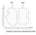
도 13a 내지 13c는 본 발명의 다양한 실시예에 따른 MST 신호 인식 성공률을 도시한다.
도 13d는, 도 13a 내지 13c의 결과 중, 녹색 사각형의 영역만을 분리하여 비교한 결과를 도시한다.
도 14a 내지 14f는 본 발명의 다양한 실시예에 따른 3층 구조의 코일을 도시한다.
도 15a 내지 15c는, 본 발명의 다양한 실시예에 따른 3층 구조의 코일과 3층 구조의 비교예의 성능 비교를 위한 위치별 인식 성공률에 대하여 도시한다.
도 15d는 본 발명에 의한 2층 구조의 코일 및 3층 구조의 코일의 인식 성공률을 도시한다.
도 16a 및 16b는 웨어러블 전자 장치, 예를 들어 손목시계형 웨어러블 전자 장치에 배치되는 코일의 형태를 도시한다.
도 17a 내지 17c는 본 발명의 다양한 실시예에 따른 3층 구조의 코일을 도시한다.
도 18a 및 18b는, 본 발명의 다양한 실시예에 따른 2층 구조의 원형 코일과 3층 구조의 원형 코일의 성능 비교를 위한 위치별 인식 성공률에 대하여 도시한다.
도 18c 및 18d는, 도 18a 및 18b의 결과 중, 녹색 사각형의 영역만을 분리하여 비교한 결과를 도시한다.
도 19 및 20은 본 발명의 다양한 2층 구조의 원형 코일 및 3층 구조의 원형 코일을 도시한다.
도 21은 본 발명의 다양한 실시예에 따른 전자 장치의 블록도를 도시한다.
도 22는 본 발명의 다양한 실시예에 따른 전자 장치의 케이스를 연 경우의, 전자 장치의 배면의 사시도를 도시한다.
도 23은 본 발명의 다양한 실시예에 따른 전자 장치의 단면도를 도시한다.
도 24는 본 발명의 다양한 실시예에 따른 2층 구조의 코일 및 3층 구조의 코일이 배치되는 FPCB의 적층 구조를 도시한다.
도 25는 본 발명의 다양한 실시예에 따른 코일 패턴의 평면도를 도시한다.1 shows a block diagram of an electronic device and network according to various embodiments of the present invention.
2 is a block diagram of an electronic device according to various embodiments.
3 shows a conceptual diagram for explaining MST according to various embodiments of the present invention.
4 shows a flowchart of an operation of an electronic device according to various embodiments of the present disclosure.
5 shows a conceptual diagram of a coil according to various embodiments of the present invention.
6A shows a plan view of a coil disposed on a first board according to various embodiments of the present invention.
6B shows a plan view of a coil disposed on a second board according to various embodiments of the present invention.
6C is a plan view in which coils disposed on the first board and the second board are overlapped.
7 is a plan view for explaining the position of a conductor according to various embodiments of the present disclosure.
8A and 8B are conceptual diagrams for explaining an increase in the degree of freedom of arrangement of electronic devices according to various embodiments of the present disclosure.
9A is a plan view illustrating a coil disposed on a second board according to various embodiments of the present disclosure.
9B is a perspective view illustrating a structure in which an additional coil is disposed according to various embodiments of the present disclosure.
10A is a plan view of a first layer in which a plurality of coils for various purposes are disposed according to various embodiments of the present invention.
10B is a plan view of a second layer in which a plurality of coils for various purposes are disposed according to various embodiments of the present invention.
Fig. 10C is a plan view in which the structure of the first layer of Fig. 10A and the structure of the second layer of Fig. 10B are overlapped.
11A to 11C are conceptual diagrams for explaining a connection relationship in a connection unit of a coil according to various embodiments of the present disclosure.
12A and 12B show a coil structure according to a comparative example for comparison with the present invention.
13A to 13C show MST signal recognition success rates according to various embodiments of the present invention.
FIG. 13D shows a result obtained by separating and comparing only the green square area among the results of FIGS. 13A to 13C .
14a to 14f show a coil having a three-layer structure according to various embodiments of the present invention.
15A to 15C illustrate recognition success rates for each location for performance comparison between a three-layered coil and a comparative example having a three-layered structure according to various embodiments of the present disclosure.
15D shows recognition success rates of a two-layer coil and a three-layer coil according to the present invention.
16A and 16B illustrate a shape of a coil disposed in a wearable electronic device, for example, a wristwatch type wearable electronic device.
17A to 17C show coils having a three-layer structure according to various embodiments of the present invention.
18A and 18B illustrate recognition success rates for each location for performance comparison between a two-layer circular coil and a three-layer circular coil according to various embodiments of the present disclosure.
18C and 18D show the results obtained by separating and comparing only the green square area among the results of FIGS. 18A and 18B.
19 and 20 show various two-layer circular coils and three-layer circular coils of the present invention.
21 shows a block diagram of an electronic device according to various embodiments of the present invention.
22 is a perspective view of a rear surface of an electronic device when a case of the electronic device is opened according to various embodiments of the present disclosure.
23 is a cross-sectional view of an electronic device according to various embodiments of the present disclosure.
24 illustrates a laminated structure of an FPCB in which a two-layer coil and a three-layer coil are disposed according to various embodiments of the present disclosure.
25 illustrates a plan view of a coil pattern according to various embodiments of the present disclosure.
이하, 본 문서의 다양한 실시예가 첨부된 도면을 참조하여 기재된다. 그러나, 이는 본 문서에 기재된 기술을 특정한 실시 형태에 대해 한정하려는 것이 아니며, 본 문서의 실시예의 다양한 변경(modifications), 균등물(equivalents), 및/또는 대체물(alternatives)을 포함하는 것으로 이해되어야 한다. 도면의 설명과 관련하여, 유사한 구성요소에 대해서는 유사한 참조 부호가 사용될 수 있다.Hereinafter, various embodiments of this document will be described with reference to the accompanying drawings. However, this is not intended to limit the technology described in this document to specific embodiments, and should be understood to include various modifications, equivalents, and/or alternatives of the embodiments of this document. . In connection with the description of the drawings, like reference numerals may be used for like elements.
본 문서에서, "가진다," "가질 수 있다," "포함한다," 또는 "포함할 수 있다" 등의 표현은 해당 특징(예: 수치, 기능, 동작, 또는 부품 등의 구성요소)의 존재를 가리키며, 추가적인 특징의 존재를 배제하지 않는다.In this document, expressions such as "has," "may have," "includes," or "may include" indicate the existence of a corresponding feature (eg, numerical value, function, operation, or component such as a part). , which does not preclude the existence of additional features.
본 문서에서, "A 또는 B," "A 또는/및 B 중 적어도 하나," 또는 "A 또는/및 B 중 하나 또는 그 이상"등의 표현은 함께 나열된 항목들의 모든 가능한 조합을 포함할 수 있다. 예를 들면, "A 또는 B," "A 및 B 중 적어도 하나," 또는 "A 또는 B 중 적어도 하나"는, (1) 적어도 하나의 A를 포함, (2) 적어도 하나의 B를 포함, 또는 (3) 적어도 하나의 A 및 적어도 하나의 B 모두를 포함하는 경우를 모두 지칭할 수 있다.In this document, expressions such as “A or B,” “at least one of A and/and B,” or “one or more of A or/and B” may include all possible combinations of the items listed together. . For example, “A or B,” “at least one of A and B,” or “at least one of A or B” (1) includes at least one A, (2) includes at least one B, Or (3) may refer to all cases including at least one A and at least one B.
본 문서에서 사용된 "제 1," "제 2," "첫째," 또는 "둘째,"등의 표현들은 다양한 구성요소들을, 순서 및/또는 중요도에 상관없이 수식할 수 있고, 한 구성요소를 다른 구성요소와 구분하기 위해 사용될 뿐 해당 구성요소들을 한정하지 않는다. 예를 들면, 제 1 사용자 기기와 제 2 사용자 기기는, 순서 또는 중요도와 무관하게, 서로 다른 사용자 기기를 나타낼 수 있다. 예를 들면, 본 문서에 기재된 권리 범위를 벗어나지 않으면서 제 1 구성요소는 제 2 구성요소로 명명될 수 있고, 유사하게 제 2 구성요소도 제 1 구성요소로 바꾸어 명명될 수 있다.Expressions such as "first," "second," "first," or "second," as used in this document may modify various elements, regardless of order and/or importance, and refer to one element as It is used only to distinguish it from other components and does not limit the corresponding components. For example, a first user device and a second user device may represent different user devices regardless of order or importance. For example, without departing from the scope of rights described in this document, a first element may be called a second element, and similarly, the second element may also be renamed to the first element.
어떤 구성요소(예: 제 1 구성요소)가 다른 구성요소(예: 제 2 구성요소)에 "(기능적으로 또는 통신적으로) 연결되어((operatively or communicatively) coupled with/to)" 있다거나 "접속되어(connected to)" 있다고 언급된 때에는, 상기 어떤 구성요소가 상기 다른 구성요소에 직접적으로 연결되거나, 다른 구성요소(예: 제 3 구성요소)를 통하여 연결될 수 있다고 이해되어야 할 것이다. 반면에, 어떤 구성요소(예: 제 1 구성요소)가 다른 구성요소(예: 제 2 구성요소)에 "직접 연결되어" 있다거나 "직접 접속되어" 있다고 언급된 때에는, 상기 어떤 구성요소와 상기 다른 구성요소 사이에 다른 구성요소(예: 제 3 구성요소)가 존재하지 않는 것으로 이해될 수 있다.A component (e.g., a first component) is "(operatively or communicatively) coupled with/to" another component (e.g., a second component); When referred to as "connected to", it should be understood that the certain component may be directly connected to the other component or connected through another component (eg, a third component). On the other hand, when an element (eg, a first element) is referred to as being “directly connected” or “directly connected” to another element (eg, a second element), the element and the above It may be understood that other components (eg, a third component) do not exist between the other components.
본 문서에서 사용된 표현 "~하도록 구성된(또는 설정된)(configured to)"은 상황에 따라, 예를 들면, "~에 적합한(suitable for)," "~하는 능력을 가지는(having the capacity to)," "~하도록 설계된(designed to)," "~하도록 변경된(adapted to)," "~하도록 만들어진(made to)," 또는 "~를 할 수 있는(capable of)"과 바꾸어 사용될 수 있다. 용어 "~하도록 구성된(또는 설정된)"은 하드웨어적으로 "특별히 설계된(specifically designed to)" 것만을 반드시 의미하지 않을 수 있다. 대신, 어떤 상황에서는, "~하도록 구성된 장치"라는 표현은, 그 장치가 다른 장치 또는 부품들과 함께 "~할 수 있는" 것을 의미할 수 있다. 예를 들면, 문구 "A, B, 및 C를 수행하도록 구성된(또는 설정된) 프로세서"는 해당 동작을 수행하기 위한 전용 프로세서(예: 임베디드 프로세서), 또는 메모리 장치에 저장된 하나 이상의 소프트웨어 프로그램들을 실행함으로써, 해당 동작들을 수행할 수 있는 범용 프로세서(generic-purpose processor)(예: CPU 또는 application processor)를 의미할 수 있다.As used in this document, the expression "configured to" means "suitable for," "having the capacity to," depending on the circumstances. ," "designed to," "adapted to," "made to," or "capable of." The term "configured (or set) to" may not necessarily mean only "specifically designed to" hardware. Instead, in some contexts, the phrase "device configured to" may mean that the device is "capable of" in conjunction with other devices or components. For example, the phrase "a processor configured (or configured) to perform A, B, and C" may include a dedicated processor (eg, embedded processor) to perform the operation, or by executing one or more software programs stored in a memory device. , may mean a general-purpose processor (eg, CPU or application processor) capable of performing corresponding operations.
본 문서에서 사용된 용어들은 단지 특정한 실시예를 설명하기 위해 사용된 것으로, 다른 실시예의 범위를 한정하려는 의도가 아닐 수 있다. 단수의 표현은 문맥상 명백하게 다르게 뜻하지 않는 한, 복수의 표현을 포함할 수 있다. 기술적이거나 과학적인 용어를 포함해서 여기서 사용되는 용어들은 본 문서에 기재된 기술 분야에서 통상의 지식을 가진 자에 의해 일반적으로 이해되는 것과 동일한 의미를 가질 수 있다. 본 문서에 사용된 용어들 중 일반적인 사전에 정의된 용어들은, 관련 기술의 문맥상 가지는 의미와 동일 또는 유사한 의미로 해석될 수 있으며, 본 문서에서 명백하게 정의되지 않는 한, 이상적이거나 과도하게 형식적인 의미로 해석되지 않는다. 경우에 따라서, 본 문서에서 정의된 용어일지라도 본 문서의 실시예들을 배제하도록 해석될 수 없다.Terms used in this document are only used to describe a specific embodiment, and may not be intended to limit the scope of other embodiments. Singular expressions may include plural expressions unless the context clearly dictates otherwise. Terms used herein, including technical or scientific terms, may have the same meaning as commonly understood by a person of ordinary skill in the technical field described in this document. Among the terms used in this document, terms defined in a general dictionary may be interpreted as having the same or similar meaning as the meaning in the context of the related art, and unless explicitly defined in this document, an ideal or excessively formal meaning. not be interpreted as In some cases, even terms defined in this document cannot be interpreted to exclude the embodiments of this document.
본 문서의 다양한 실시예들에 따른 전자 장치는, 예를 들면, 스마트폰(smartphone), 태블릿 PC(tablet personal computer), 이동 전화기(mobile phone), 영상 전화기, 전자책 리더기(e-book reader), 데스크탑 PC(desktop personal computer), 랩탑 PC(laptop personal computer), 넷북 컴퓨터(netbook computer), 워크스테이션(workstation), 서버, PDA(personal digital assistant), PMP(portable multimedia player), MP3 플레이어, 모바일 의료기기, 카메라(camera), 또는 웨어러블 장치(wearable device) 중 적어도 하나를 포함할 수 있다. 다양한 실시예에 따르면, 웨어러블 장치는 액세서리형(예: 시계, 반지, 팔찌, 발찌, 목걸이, 안경, 콘택트 렌즈, 또는 머리 착용형 장치(head-mounted-device(HMD)), 직물 또는 의류 일체형(예: 전자 의복), 신체 부착형(예: 스킨 패드(skin pad) 또는 문신), 또는 생체 이식형(예: implantable circuit) 중 적어도 하나를 포함할 수 있다. 한편, 전자 장치는 무선으로 무선 전력 송신기로부터 전력을 수신할 수도 있으며, 이에 따라 전자 장치는 무선 전력 수신기로 명명될 수 있다.Electronic devices according to various embodiments of the present document include, for example, a smartphone, a tablet personal computer (PC), a mobile phone, a video phone, and an e-book reader. , desktop personal computer (laptop personal computer), netbook computer, workstation, server, PDA (personal digital assistant), PMP (portable multimedia player), MP3 player, mobile It may include at least one of a medical device, a camera, or a wearable device. According to various embodiments, the wearable device may be an accessory (eg, watch, ring, bracelet, anklet, necklace, glasses, contact lens, or head-mounted-device (HMD)), fabric or clothing integrated ( The electronic device may include at least one of a body-attached type (eg, a skin pad or tattoo), or an implantable circuit (eg, an implantable circuit). Power may be received from the transmitter, and thus the electronic device may be referred to as a wireless power receiver.
어떤 실시예들에서, 전자 장치는 가전 제품(home appliance)일 수 있다. 가전 제품은, 예를 들면, 텔레비전, DVD(digital video disk) 플레이어, 오디오, 냉장고, 에어컨, 청소기, 오븐, 전자레인지, 세탁기, 공기 청정기, 셋톱 박스(set-top box), 홈 오토매이션 컨트롤 패널(home automation control panel), 보안 컨트롤 패널(security control panel), TV 박스(예: 삼성 HomeSyncTM, 애플TVTM, 또는 구글 TVTM), 게임 콘솔(예: XboxTM, PlayStationTM), 전자 사전, 전자 키, 캠코더(camcorder), 또는 전자 액자 중 적어도 하나를 포함할 수 있다.In some embodiments, the electronic device may be a home appliance. Home appliances include, for example, televisions, digital video disk (DVD) players, audio systems, refrigerators, air conditioners, vacuum cleaners, ovens, microwave ovens, washing machines, air purifiers, set-top boxes, and home automation controls. Home automation control panel, security control panel, TV box (eg Samsung HomeSyncTM , Apple TVTM , or Google TVTM ), game console (eg XboxTM , PlayStationTM ), electronic dictionary , an electronic key, a camcorder, or an electronic picture frame.
다른 실시예에서, 전자 장치는, 각종 의료기기(예: 각종 휴대용 의료측정기기(혈당 측정기, 심박 측정기, 혈압 측정기, 또는 체온 측정기 등), MRA(magnetic resonance angiography), MRI(magnetic resonance imaging), CT(computed tomography), 촬영기, 또는 초음파기 등), 네비게이션(navigation) 장치, 위성 항법 시스템(GNSS(global navigation satellite system)), EDR(event data recorder), FDR(flight data recorder), 자동차 인포테인먼트(infotainment) 장치, 선박용 전자 장비(예: 선박용 항법 장치, 자이로 콤파스 등), 항공 전자기기(avionics), 보안 기기, 차량용 헤드 유닛(head unit), 산업용 또는 가정용 로봇, 금융 기관의 ATM(automatic teller's machine), 상점의 POS(point of sales), 또는 사물 인터넷 장치(internet of things)(예: 전구, 각종 센서, 전기 또는 가스 미터기, 스프링클러 장치, 화재경보기, 온도조절기(thermostat), 가로등, 토스터(toaster), 운동기구, 온수탱크, 히터, 보일러 등) 중 적어도 하나를 포함할 수 있다.In another embodiment, the electronic device may include various types of medical devices (e.g., various portable medical measuring devices (such as blood glucose meter, heart rate monitor, blood pressure monitor, or body temperature monitor), magnetic resonance angiography (MRA), magnetic resonance imaging (MRI), CT (computed tomography), imager, or ultrasonicator, etc.), navigation device, GNSS (global navigation satellite system), EDR (event data recorder), FDR (flight data recorder), automotive infotainment ) devices, marine electronics (e.g. marine navigation systems, gyrocompasses, etc.), avionics, security devices, automotive head units, industrial or home robots, automatic teller's machines (ATMs) of financial institutions , point of sales (POS) in stores, or internet of things devices (e.g. light bulbs, sensors, electric or gas meters, sprinklers, smoke alarms, thermostats, street lights, toasters) , Exercise equipment, hot water tank, heater, boiler, etc.) may include at least one.
어떤 실시예에 따르면, 전자 장치는 가구(furniture) 또는 건물/구조물의 일부, 전자 보드(electronic board), 전자 사인 수신 장치(electronic signature receiving device), 프로젝터(projector), 또는 각종 계측 기기(예: 수도, 전기, 가스, 또는 전파 계측 기기 등) 중 적어도 하나를 포함할 수 있다. 다양한 실시예에서, 전자 장치는 전술한 다양한 장치들 중 하나 또는 그 이상의 조합일 수 있다. 어떤 실시예에 따른 전자 장치는 플렉서블 전자 장치일 수 있다. 또한, 본 문서의 실시예에 따른 전자 장치는 전술한 기기들에 한정되지 않으며, 기술 발전에 따른 새로운 전자 장치를 포함할 수 있다.According to some embodiments, the electronic device is a piece of furniture or a building/structure, an electronic board, an electronic signature receiving device, a projector, or various measuring devices (eg, Water, electricity, gas, radio wave measuring devices, etc.) may include at least one. In various embodiments, the electronic device may be a combination of one or more of the various devices described above. An electronic device according to some embodiments may be a flexible electronic device. In addition, the electronic device according to the embodiment of this document is not limited to the above-described devices, and may include new electronic devices according to technological development.
이하, 첨부 도면을 참조하여, 다양한 실시예에 따른 전자 장치가 설명된다. 본 문서에서, 사용자라는 용어는 전자 장치를 사용하는 사람 또는 전자 장치를 사용하는 장치(예: 인공지능 전자 장치)를 지칭할 수 있다.Hereinafter, an electronic device according to various embodiments will be described with reference to the accompanying drawings. In this document, the term user may refer to a person using an electronic device or a device using an electronic device (eg, an artificial intelligence electronic device).
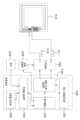
도 1을 참조하여, 다양한 실시예에서의, 네트워크 환경(100) 내의 전자 장치(101)가 기재된다. 전자 장치(101)는 버스(110), 프로세서(120), 메모리(130), 입출력 인터페이스(150), 디스플레이(160), 통신 모듈(170), 무선 충전 모듈(180) 및 MST 모듈(190)을 포함할 수 있다. 어떤 실시예에서는, 전자 장치(101)는, 구성요소들 중 적어도 하나를 생략하거나 다른 구성요소를 추가적으로 구비할 수 있다.Referring to FIG. 1 , an
버스(110)는, 예를 들면, 구성요소들(110-170)을 서로 연결하고, 구성요소들 간의 통신(예: 제어 메시지 및/또는 데이터)을 전달하는 회로를 포함할 수 있다.
프로세서(120)는, 중앙처리장치(central processing unit(CPU)), 어플리케이션 프로세서(application processor(AP)), 또는 커뮤니케이션 프로세서(communication processor(CP)) 중 하나 또는 그 이상을 포함할 수 있다. 프로세서(120)는, 예를 들면, 전자 장치(101)의 적어도 하나의 다른 구성요소들의 제어 및/또는 통신에 관한 연산이나 데이터 처리를 실행할 수 있다.The
메모리(130)는, 휘발성 및/또는 비휘발성 메모리를 포함할 수 있다. 메모리(130)는, 예를 들면, 전자 장치(101)의 적어도 하나의 다른 구성요소에 관계된 명령 또는 데이터를 저장할 수 있다. 한 실시예에 따르면, 메모리(130)는 소프트웨어 및/또는 프로그램(140)을 저장할 수 있다. 프로그램(140)은, 예를 들면, 커널(141), 미들웨어(143), 어플리케이션 프로그래밍 인터페이스(application programming interface(API))(145), 및/또는 어플리케이션 프로그램(또는 "어플리케이션")(147) 등을 포함할 수 있다. 커널(141), 미들웨어(143), 또는 API(145)의 적어도 일부는, 운영 시스템(operating system(OS))으로 지칭될 수 있다.
커널(141)은, 예를 들면, 다른 프로그램들(예: 미들웨어(143), API(145), 또는 어플리케이션 프로그램(147))에 구현된 동작 또는 기능을 실행하는 데 사용되는 시스템 리소스들(예: 버스(110), 프로세서(120), 또는 메모리(130) 등)을 제어 또는 관리할 수 있다. 또한, 커널(141)은 미들웨어(143), API(145), 또는 어플리케이션 프로그램(147)에서 전자 장치(101)의 개별 구성요소에 접근함으로써, 시스템 리소스들을 제어 또는 관리할 수 있는 인터페이스를 제공할 수 있다.
미들웨어(143)는, 예를 들면, API(145) 또는 어플리케이션 프로그램(147)이 커널(141)과 통신하여 데이터를 주고받을 수 있도록 중개 역할을 수행할 수 있다.The
또한, 미들웨어(143)는 어플리케이션 프로그램(147)으로부터 수신된 하나 이상의 작업 요청들을 우선 순위에 따라 처리할 수 있다. 예를 들면, 미들웨어(143)는 어플리케이션 프로그램(147) 중 적어도 하나에 전자 장치(101)의 시스템 리소스(예: 버스(110), 프로세서(120), 또는 메모리(130) 등)를 사용할 수 있는 우선 순위를 부여할 수 있다. 예컨대, 미들웨어(143)는 상기 적어도 하나에 부여된 우선 순위에 따라 상기 하나 이상의 작업 요청들을 처리함으로써, 상기 하나 이상의 작업 요청들에 대한 스케쥴링 또는 로드 밸런싱 등을 수행할 수 있다.Also, the
API(145)는, 예를 들면, 어플리케이션(147)이 커널(141) 또는 미들웨어(143)에서 제공되는 기능을 제어하기 위한 인터페이스로, 예를 들면, 파일 제어, 창 제어, 영상 처리, 또는 문자 제어 등을 위한 적어도 하나의 인터페이스 또는 함수(예: 명령어)를 포함할 수 있다.The
입출력 인터페이스(150)는, 예를 들면, 사용자 또는 다른 외부 기기로부터 입력된 명령 또는 데이터를 전자 장치(101)의 다른 구성요소(들)에 전달할 수 있는 인터페이스의 역할을 할 수 있다. 또한, 입출력 인터페이스(150)는 전자 장치(101)의 다른 구성요소(들)로부터 수신된 명령 또는 데이터를 사용자 또는 다른 외부 기기로 출력할 수 있다.The input/
디스플레이(160)는, 예를 들면, 액정 디스플레이(liquid crystal display(LCD)), 발광 다이오드(light-emitting diode(LED)) 디스플레이, 유기 발광 다이오드(organic light-emitting diode(OLED)) 디스플레이, 또는 마이크로 전자기계 시스템(microelectromechanical systems(MEMS)) 디스플레이, 또는 전자종이(electronic paper) 디스플레이를 포함할 수 있다. 디스플레이(160)는, 예를 들면, 사용자에게 각종 콘텐츠(예: 텍스트, 이미지, 비디오, 아이콘, 또는 심볼 등)을 표시할 수 있다. 디스플레이(160)는, 터치 스크린을 포함할 수 있으며, 예를 들면, 전자 펜 또는 사용자의 신체의 일부를 이용한 터치, 제스쳐, 근접, 또는 호버링 입력을 수신할 수 있다.The
통신 모듈(170)은, 예를 들면, 전자 장치(101)와 외부 장치(예: 제 1 외부 전자 장치(102), 제 2 외부 전자 장치(104), 또는 서버(106)) 간의 통신을 설정할 수 있다. 예를 들면, 통신 모듈(170)은 무선 통신 또는 유선 통신을 통해서 네트워크(162)에 연결되어 외부 장치(예: 제 2 외부 전자 장치(104) 또는 서버(106))와 통신할 수 있다.The
무선 통신은, 예를 들면, 셀룰러 통신 프로토콜로서, 예를 들면, LTE(long-term evolution), LTE-A(LTE Advance), CDMA(code division multiple access), WCDMA(wideband CDMA), UMTS(universal mobile telecommunications system), WiBro(Wireless Broadband), 또는 GSM(Global System for Mobile Communications) 등 중 적어도 하나를 사용할 수 있다. 또한, 무선 통신은, 예를 들면, 근거리 통신(164)을 포함할 수 있다. 근거리 통신(164)은, 예를 들면, WiFi(wireless fidelity), 블루투스(Bluetooth), NFC(near field communication), 또는 GNSS(global navigation satellite system) 등 중 적어도 하나를 포함할 수 있다. GNSS는 사용 지역 또는 대역폭 등에 따라, 예를 들면, GPS(Global Positioning System), Glonass(Global Navigation Satellite System), Beidou Navigation Satellite System(이하 "Beidou") 또는 Galileo, the European global satellite-based navigation system 중 적어도 하나를 포함할 수 있다. 이하, 본 문서에서는, "GPS"는 "GNSS"와 혼용되어 사용(interchangeably used)될 수 있다. 유선 통신은, 예를 들면, USB(universal serial bus), HDMI(high definition multimedia interface), RS-232(recommended standard232), 또는 POTS(plain old telephone service) 등 중 적어도 하나를 포함할 수 있다. 네트워크(162)는 통신 네트워크(telecommunications network), 예를 들면, 컴퓨터 네트워크(computer network)(예: LAN 또는 WAN), 인터넷, 또는 전화 망(telephone network) 중 적어도 하나를 포함할 수 있다.Wireless communication is, for example, a cellular communication protocol, for example, long-term evolution (LTE), LTE Advance (LTE-A), code division multiple access (CDMA), wideband CDMA (WCDMA), universal At least one of a mobile telecommunications system), WiBro (Wireless Broadband), GSM (Global System for Mobile Communications), and the like may be used. Wireless communication may also include, for example, near
무선 충전 모듈(180)은 무선 전력 수신기로부터 무선 전력을 수신하거나, 다른 전자 장치로 무선 전력을 송신할 수 있다. 무선 충전 모듈(180)은 유도 방식 또는 공진 방식에 기초하여, 무선 전력을 수신하거나 송신할 수 있다. 무선 충전 모듈(180)은 무선 전력의 송/수신을 위한 코일을 포함할 수도 있다.The
MST 모듈(190)은 다른 전자 장치와 MST를 수행할 수 있다. MST를 수행한다는 것은, 시간에 따라 크기가 변경되는 자기장(191)을 형성하는 것을 의미할 수 있다. 예를 들어, MST 모듈(190)은 시간에 따라 크기가 변경되는 자기장(191)을 방출할 수 있으며, 시간에 따라 크기가 변경된다는 것은 정보를 포함하는 신호를 송신하는 것과 동일할 수 있다. 다른 전자 장치, 예를 들어 POS 단말기는, 자기장(191)의 시간에 따른 크기 변경을 검출함으로써, 전자 장치(101)로부터의 정보를 포함하는 신호를 수신할 수 있다. 한편, MST 모듈(190)은 자기장 방출을 위한 코일을 포함할 수도 있다. MST 모듈(190)은 다른 전자 장치로부터 수신되는 자기장의 시간에 따른 변경을 검출함으로써, 다른 전자 장치로부터 신호를 수신할 수도 있다.The MST module 190 may perform MST with other electronic devices. Performing MST may mean forming a
제 1 및 제 2 외부 전자 장치(102, 104) 각각은 전자 장치(101)와 동일한 또는 다른 종류의 장치일 수 있다. 한 실시예에 따르면, 서버(106)는 하나 또는 그 이상의 서버들의 그룹을 포함할 수 있다. 다양한 실시예에 따르면, 전자 장치(101)에서 실행되는 동작들의 전부 또는 일부는 다른 하나 또는 복수의 전자 장치(예: 전자 장치(102,104), 또는 서버(106)에서 실행될 수 있다. 한 실시예에 따르면, 전자 장치(101)가 어떤 기능이나 서비스를 자동으로 또는 요청에 의하여 수행해야 할 경우에, 전자 장치(101)는 기능 또는 서비스를 자체적으로 실행시키는 대신에 또는 추가적으로, 그와 연관된 적어도 일부 기능을 다른 장치(예: 전자 장치(102, 104), 또는 서버(106))에게 요청할 수 있다. 다른 전자 장치(예: 전자 장치(102, 104), 또는 서버(106))는 요청된 기능 또는 추가 기능을 실행하고, 그 결과를 전자 장치(101)로 전달할 수 있다. 전자 장치(101)는 수신된 결과를 그대로 또는 추가적으로 처리하여 요청된 기능이나 서비스를 제공할 수 있다. 이를 위하여, 예를 들면, 클라우드 컴퓨팅, 분산 컴퓨팅, 또는 클라이언트-서버 컴퓨팅 기술이 이용될 수 있다.Each of the first and second external
도 2는 다양한 실시예에 따른 전자 장치(201)의 블록도이다. 전자 장치(201)는, 예를 들면, 도 1에 도시된 전자 장치(101)의 전체 또는 일부를 포함할 수 있다. 전자 장치(201)는 하나 이상의 프로세서(예: AP(application processor))(210), 통신 모듈(220), MST 모듈(222) 가입자 식별 모듈(224), 메모리(230), 센서 모듈(240), 입력 장치(250), 디스플레이(260), 인터페이스(270), 오디오 모듈(280), 카메라 모듈(291), 전력 관리 모듈(295), 배터리(296), 인디케이터(297), 모터(298), 및 무선 충전 모듈(299)을 포함할 수 있다.2 is a block diagram of an electronic device 201 according to various embodiments. The electronic device 201 may include, for example, all or part of the
프로세서(210)는, 예를 들면, 운영 체제 또는 응용 프로그램을 구동하여 프로세서(210)에 연결된 다수의 하드웨어 또는 소프트웨어 구성요소들을 제어할 수 있고, 각종 데이터 처리 및 연산을 수행할 수 있다. 프로세서(210)는, 예를 들면, SoC(system on chip) 로 구현될 수 있다. 한 실시예에 따르면, 프로세서(210)는 GPU(graphic processing unit) 및/또는 이미지 신호 프로세서(image signal processor)를 더 포함할 수 있다. 프로세서(210)는 도 2에 도시된 구성요소들 중 적어도 일부(예: 셀룰러 모듈(221))를 포함할 수도 있다. 프로세서(210) 는 다른 구성요소들(예: 비휘발성 메모리) 중 적어도 하나로부터 수신된 명령 또는 데이터를 휘발성 메모리에 로드(load)하여 처리하고, 다양한 데이터를 비휘발성 메모리에 저장(store)할 수 있다.The
통신 모듈(220)은, 도 1의 통신 모듈(170)과 동일 또는 유사한 구성을 가질 수 있다. 통신 모듈(220)은, 예를 들면, 셀룰러 모듈(221), WiFi 모듈(223), 블루투스 모듈(225), GNSS 모듈(227)(예: GPS 모듈, Glonass 모듈, Beidou 모듈, 또는 Galileo 모듈), NFC 모듈(228) 및 RF(radio frequency) 모듈(229)를 포함할 수 있다.The
셀룰러 모듈(221)은, 예를 들면, 통신망을 통해서 음성 통화, 영상 통화, 문자 서비스, 또는 인터넷 서비스 등을 제공할 수 있다. 한 실시예에 따르면, 셀룰러 모듈(221)은 가입자 식별 모듈(예: SIM 카드)(224)을 이용하여 통신 네트워크 내에서 전자 장치(201)의 구별 및 인증을 수행할 수 있다. 한 실시예에 따르면, 셀룰러 모듈(221)은 프로세서(210)가 제공할 수 있는 기능 중 적어도 일부 기능을 수행할 수 있다. 한 실시예에 따르면, 셀룰러 모듈(221)은 커뮤니케이션 프로세서(CP: communication processor)를 포함할 수 있다.The cellular module 221 may provide, for example, a voice call, a video call, a text service, or an Internet service through a communication network. According to one embodiment, the cellular module 221 may identify and authenticate the electronic device 201 within a communication network using the subscriber identity module (eg, SIM card) 224 . According to one embodiment, the cellular module 221 may perform at least some of the functions that the
WiFi 모듈(223), 블루투스 모듈(225), GNSS 모듈(227) 또는 NFC 모듈(228) 각각은, 예를 들면, 해당하는 모듈을 통해서 송수신되는 데이터를 처리하기 위한 프로세서를 포함할 수 있다. 어떤 실시예에 따르면, 셀룰러 모듈(221), WiFi 모듈(223), 블루투스 모듈(225), GNSS 모듈(227) 또는 NFC 모듈(228) 중 적어도 일부(예: 두 개 이상)는 하나의 integrated circuit(IC) 또는 IC 패키지 내에 포함될 수 있다.Each of the WiFi module 223, the Bluetooth module 225, the GNSS module 227, or the NFC module 228 may include, for example, a processor for processing data transmitted and received through the corresponding module. According to some embodiments, at least some (eg, two or more) of the cellular module 221, the WiFi module 223, the Bluetooth module 225, the GNSS module 227, or the NFC module 228 are integrated circuits. (IC) or within an IC package.
RF 모듈(229)은, 예를 들면, 통신 신호(예: RF 신호)를 송수신할 수 있다. RF 모듈(229)은, 예를 들면, 트랜시버(transceiver), PAM(power amp module), 주파수 필터(frequency filter), LNA(low noise amplifier), 또는 안테나 등을 포함할 수 있다. 다른 실시예에 따르면, 셀룰러 모듈(221), WiFi 모듈(223), 블루투스 모듈(225), GNSS 모듈(227) 또는 NFC 모듈(228) 중 적어도 하나는 별개의 RF 모듈을 통하여 RF 신호를 송수신할 수 있다.The
가입자 식별 모듈(224)은, 예를 들면, 가입자 식별 모듈을 포함하는 카드 및/또는 내장 SIM(embedded SIM)을 포함할 수 있으며, 고유한 식별 정보(예: ICCID(integrated circuit card identifier)) 또는 가입자 정보(예: IMSI(international mobile subscriber identity))를 포함할 수 있다.The
MST 모듈(222)은 자기장을 이용하는 신호를 송수신할 수 있으며, 예를 들어 결제 정보와 같은 정보를 포함하는 신호를 송수신할 수 있다. MST 모듈(222)은 시간에 따라 크기가 변경되는 자기장을 방출하거나, 수신되는 자기장으로부터의 유도 전류에 기초하여 통신을 수행할 수 있다.The
메모리(230)(예: 메모리(130))는, 예를 들면, 내장 메모리(232) 또는 외장 메모리(234)를 포함할 수 있다. 내장 메모리(232)는, 예를 들면, 휘발성 메모리(예: DRAM(dynamic RAM), SRAM(static RAM), 또는 SDRAM(synchronous dynamic RAM) 등), 비휘발성 메모리(non-volatile Memory)(예: OTPROM(one time programmable ROM), PROM(programmable ROM), EPROM(erasable and programmable ROM), EEPROM(electrically erasable and programmable ROM), mask ROM, flash ROM, 플래시 메모리(예: NAND flash 또는 NOR flash 등), 하드 드라이브, 또는 솔리드 스테이트 드라이브(solid state drive(SSD)) 중 적어도 하나를 포함할 수 있다.The memory 230 (eg, the memory 130) may include, for example, an
외장 메모리(234)는 플래시 드라이브(flash drive), 예를 들면, CF(compact flash), SD(secure digital), Micro-SD(micro secure digital), Mini-SD(mini secure digital), xD(extreme digital), MMC(multi-media card) 또는 메모리 스틱(memory stick) 등을 더 포함할 수 있다. 외장 메모리(234)는 다양한 인터페이스를 통하여 전자 장치(201)와 기능적으로 및/또는 물리적으로 연결될 수 있다.The
센서 모듈(240)은, 예를 들면, 물리량을 계측하거나 전자 장치(201)의 작동 상태를 감지하여, 계측 또는 감지된 정보를 전기 신호로 변환할 수 있다. 센서 모듈(240)은, 예를 들면, 제스처 센서(240A), 자이로 센서(240B), 기압 센서(240C), 마그네틱 센서(240D), 가속도 센서(240E), 그립 센서(240F), 근접 센서(240G), 컬러(color) 센서(240H)(예: RGB(red, green, blue) 센서), 생체 센서(240I), 온/습도 센서(240J), 조도 센서(240K), 또는 UV(ultra violet) 센서(240M) 중의 적어도 하나를 포함할 수 있다. 추가적으로 또는 대체적으로(additionally or alternatively), 센서 모듈(240)은, 예를 들면, 후각 센서(E-nose sensor), EMG 센서(electromyography sensor), EEG 센서(electroencephalogram sensor), ECG 센서(electrocardiogram sensor), IR(infrared) 센서, 홍채 센서 및/또는 지문 센서를 포함할 수 있다. 센서 모듈(240)은 그 안에 속한 적어도 하나 이상의 센서들을 제어하기 위한 제어 회로를 더 포함할 수 있다. 어떤 실시예에서는, 전자 장치(201)는 프로세서(210)의 일부로서 또는 별도로, 센서 모듈(240)을 제어하도록 구성된 프로세서를 더 포함하여, 프로세서(210)가 슬립(sleep) 상태에 있는 동안, 센서 모듈(240)을 제어할 수 있다.The
입력 장치(250)는, 예를 들면, 터치 패널(touch panel)(252),(디지털) 펜 센서(pen sensor)(254), 키(key)(256), 또는 초음파(ultrasonic) 입력 장치(258)를 포함할 수 있다. 터치 패널(252)은, 예를 들면, 정전식, 감압식, 적외선 방식, 또는 초음파 방식 중 적어도 하나의 방식을 사용할 수 있다. 또한, 터치 패널(252)은 제어 회로를 더 포함할 수도 있다. 터치 패널(252)은 택타일 레이어(tactile layer)를 더 포함하여, 사용자에게 촉각 반응을 제공할 수 있다.The
(디지털) 펜 센서(254)는, 예를 들면, 터치 패널의 일부이거나, 별도의 인식용 쉬트(sheet)를 포함할 수 있다. 키(256)는, 예를 들면, 물리적인 버튼, 광학식 키, 또는 키패드를 포함할 수 있다. 초음파 입력 장치(258)는 마이크(예: 마이크(288))를 통해, 입력 도구에서 발생된 초음파를 감지하여, 상기 감지된 초음파에 대응하는 데이터를 확인할 수 있다.The (digital)
디스플레이(260)(예: 디스플레이(160))는 패널(262), 홀로그램 장치(264), 또는 프로젝터(266)를 포함할 수 있다. 패널(262)은, 도 1의 디스플레이(160)와 동일 또는 유사한 구성을 포함할 수 있다. 패널(262)은, 예를 들면, 유연하게(flexible), 투명하게(transparent), 또는 착용할 수 있게(wearable) 구현될 수 있다. 패널(262)은 터치 패널(252)과 하나의 모듈로 구성될 수도 있다. 한 실시예에 따르면, 패널(262)은 사용자의 터치에 대한 압력의 세기를 측정할 수 있는 압력 센서(또는 포스 센서)를 포함할 수 있다. 상기 압력 센서는 터치 패널(252)과 일체형으로 구현되거나, 또는 터치 패널(252)과는 별도의 하나 이상의 센서로 구현될 수 있다. 홀로그램 장치(264)는 빛의 간섭을 이용하여 입체 영상을 허공에 보여줄 수 있다. 홀로그램 장치(264)는 빛의 간섭을 이용하여 입체 영상을 허공에 보여줄 수 있다. 프로젝터(266)는 스크린에 빛을 투사하여 영상을 표시할 수 있다. 스크린은, 예를 들면, 전자 장치(201)의 내부 또는 외부에 위치할 수 있다. 한 실시예에 따르면, 디스플레이(260)는 패널(262), 홀로그램 장치(264), 또는 프로젝터(266)를 제어하기 위한 제어 회로를 더 포함할 수 있다.The display 260 (eg, the display 160 ) may include a
인터페이스(270)는, 예를 들면, HDMI(high-definition multimedia interface)(272), USB(universal serial bus)(274), 광 인터페이스(optical interface)(276), 또는 D-sub(D-subminiature)(278)를 포함할 수 있다. 인터페이스(270)는, 예를 들면, 도 1에 도시된 통신 모듈(170)에 포함될 수 있다. 추가적으로 또는 대체적으로(additionally and alternatively), 인터페이스(270)는, 예를 들면, MHL(mobile high-definition link) 인터페이스, SD(secure digital) 카드/MMC(multi-media card) 인터페이스, 또는 IrDA(infrared data association) 규격 인터페이스를 포함할 수 있다.The
오디오 모듈(280)은, 예를 들면, 소리(sound)와 전기 신호를 쌍방향으로 변환시킬 수 있다. 오디오 모듈(280)의 적어도 일부 구성요소는, 예를 들면, 도 1 에 도시된 입출력 인터페이스(150)에 포함될 수 있다. 오디오 모듈(280)은, 예를 들면, 스피커(282), 리시버(284), 이어폰(286), 또는 마이크(288) 등을 통해 입력 또는 출력되는 소리 정보를 처리할 수 있다.The
카메라 모듈(291)은, 예를 들면, 정지 영상 및 동영상을 촬영할 수 있는 장치로서, 한 실시예에 따르면, 하나 이상의 이미지 센서(예: 전면 센서 또는 후면 센서), 렌즈, ISP(image signal processor), 또는 플래시(flash)(예: LED 또는 xenon lamp 등)를 포함할 수 있다.The
전력 관리 모듈(295)은, 예를 들면, 전자 장치(201)의 전력을 관리할 수 있다. 한 실시예에 따르면, 전력 관리 모듈(295)은 전력 관리 집적회로(power management integrated circuit), 충전 IC(charger integrated circuit), 또는 배터리 또는 연료 게이지(battery or fuel gauge)를 포함할 수 있다. 전력 관리 집적회로는, 유선 및/또는 무선 충전 방식을 가질 수 있다. 무선 충전 방식은, 예를 들면, 자기공명 방식, 자기유도 방식 또는 전자기파 방식 등을 포함하며, 무선 충전을 위한 부가적인 회로, 예를 들면, 코일 루프, 공진 회로, 또는 정류기 등을 더 포함할 수 있다. 배터리 게이지는, 예를 들면, 배터리(296)의 잔량, 충전 중 전압, 전류, 또는 온도를 측정할 수 있다. 배터리(296)는, 예를 들면, 충전식 전지(rechargeable battery) 및/또는 태양 전지(solar battery)를 포함할 수 있다. 전력 관리 모듈(295)은 무선 충전 모듈(299)과 연결될 수도 있다. 무선 충전 모듈(299)은 다른 전자 장치로부터 무선 전력을 수신하여, 배터리(296)를 충전할 수 있다. 또는, 무선 충전 모듈(299)은 배터리(296)로부터의 전력을 이용하여 다른 전자 장치를 무선 충전할 수도 있다. 무선 충전 모듈(299)은 배터리(296)에 직접 연결될 수도 있다.The
인디케이터(297)는 전자 장치(201) 또는 그 일부(예: 프로세서(210))의 특정 상태, 예를 들면, 부팅 상태, 메시지 상태 또는 충전 상태 등을 표시할 수 있다. 모터(298)는 전기적 신호를 기계적 진동으로 변환할 수 있고, 진동(vibration), 또는 햅틱(haptic) 효과 등을 발생시킬 수 있다. 도시되지는 않았으나, 전자 장치(201)는 모바일 TV 지원을 위한 처리 장치(예: GPU)를 포함할 수 있다. 모바일 TV 지원을 위한 처리 장치는, 예를 들면, DMB(digital multimedia broadcasting), DVB(digital video broadcasting), 또는 미디어플로(mediaFloTM) 등의 규격에 따른 미디어 데이터를 처리할 수 있다.The
본 문서에서 기술된 구성요소들 각각은 하나 또는 그 이상의 부품(component)으로 구성될 수 있으며, 해당 구성요소의 명칭은 전자 장치의 종류에 따라서 달라질 수 있다. 다양한 실시예에서, 전자 장치는 본 문서에서 기술된 구성요소 중 적어도 하나를 포함하여 구성될 수 있으며, 일부 구성요소가 생략되거나 또는 추가적인 다른 구성요소를 더 포함할 수 있다. 또한, 다양한 실시예에 따른 전자 장치의 구성요소들 중 일부가 결합되어 하나의 개체(entity)로 구성됨으로써, 결합되기 이전의 해당 구성요소들의 기능을 동일하게 수행할 수 있다.Each of the components described in this document may be composed of one or more components, and the name of the corresponding component may vary depending on the type of electronic device. In various embodiments, an electronic device may include at least one of the components described in this document, and some components may be omitted or additional components may be further included. In addition, some of the components of the electronic device according to various embodiments are combined to form a single entity, so that the functions of the corresponding components before being combined can be performed the same.
도 3은 본 발명의 다양한 실시예에 따른 MST를 설명하기 위한 개념도를 도시한다.3 shows a conceptual diagram for explaining MST according to various embodiments of the present invention.
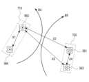
포스(POS) 단말기(301)는 마그네틱 신용카드로부터 결제 정보를 획득하여, 획득된 정보를 결제 서버로 송신할 수 있는 장치일 수 있다. 예를 들어, 포스 단말기(301)의 판독 헤더(reader header)는 신용카드의 자기 스트라이프와 같은 자기 기록 매체가 접촉하는 경우의 자기장을 센싱할 수 있다. 마그네틱 신용카드가 판독 헤더에 대하여 스와이프되는 경우에, 포스 단말기(301)가 센싱하는 자기장이 변경될 수 있으며, 포스 단말기(301)는 이를 결제 정보로서 획득할 수 있다. 즉, 포스 단말기(301)는 시간에 따라 변경하는 자기장을 결제 정보로서 획득할 수 있다.The
포스 단말기(301)는 결제 정보를 결제 서버로 송신할 수 있으며, 결제 서버는 수신한 결제 정보를 이용하여 결제 프로세싱을 수행할 수 있다. 포스 단말기(301)는 입력 장치로부터 입력되는 추가 정보(예를 들어, 결제 금액)를 결제 서버로 함께 송신할 수도 있으며, 결제 서버는 수신한 결제 정보 및 추가 정보에 기초하여 결제 승인 여부를 결정할 수 있다. 결제 서버는 결제 승인에 대한 정보 또는 결제 거부에 대한 정보를 포스 단말기(301)로 송신할 수 있으며, 포스 단말기(301)는 수신한 정보를 출력할 수 있다. 즉, 포스 단말기(301)는 결제 정보와 결제 승인 또는 거부 정보의 중계 장치일 수 있으며, 주변의 자기장 변경을 신호로서 입력받을 수 있다.The
한편, 본 발명의 다양한 실시예에 따른 전자 장치(101)는 자기장(320)을 방출할 수 있다. 전자 장치(101)는 본 발명의 다양한 실시예에 따른 복수 층의 코일을 포함할 수 있으며, 코일에 전류를 인가함으로써 자기장(320)을 방출할 수 있다. 본 발명의 다양한 실시예에서, 전자 장치(101)는 결제 어플리케이션 실행 화면(310)을 디스플레이(160)에 표시할 수 있다. 결제 어플리케이션은 미리 등록된 신용카드와 관련된 이미지(312)를 포함할 수 있으며, 결제 중임을 나타내는 오브젝트(311)를 포함할 수도 있다. 전자 장치(101)는 미리 등록된 신용카드에 대응하도록 자기장(320)을 시간에 따라 변경할 수 있으며, 이에 따라 전자 장치(101)에 의하여 생성되는 자기장(320)의 변경 패턴이 신용카드의 스와이프에 의한 자기장의 변경 패턴과 동일하거나 또는 대응될 수 있다. 즉, 시간에 따라 변경되는 자기장이 형성된다는 점에서, 전자 장치(101)가 자기장을 방출하는 것은, 신용카드가 스와이프되는 것과 동일한 효과를 가질 수 있다. 이에 따라, 사용자는 신용카드를 소지할 필요 없이 전자 장치(101)를 이용하여 결제를 진행할 수 있다.Meanwhile, the
도 4는 본 발명의 다양한 실시예에 따른 전자 장치의 동작의 흐름도를 도시한다.4 shows a flowchart of an operation of an electronic device according to various embodiments of the present disclosure.
410 동작에서, 전자 장치(101)는 결제 어플리케이션을 실행할 수 있다. 결제 어플리케이션은 신용카드와 관련된 결제 정보를 관리하며, MST 신호를 생성할 수 있는 어플리케이션이라면 제한이 없다. 420 동작에서, 전자 장치(101)는 사용자 인증을 수행할 수 있다. 전자 장치(101)는 예를 들어 미리 설정된 보안 정보의 입력을 요청하는 그래픽 사용자 인터페이스를 출력할 수 있다. 여기에서의 보안 정보는, 사용자의 지문, 목소리, 홍채 등의 생체 정보일 수도 있으며, 사용자에 의하여 미리 설정된 비밀번호 또는 패턴 등의 정보일 수도 있고, 그 종류에는 제한이 없다. 전자 장치(101)는 요청한 보안 정보를 수신할 수 있으며, 이를 미리 저장된 보안 정보와 비교함으로써 사용자 인증을 수행할 수 있다.In
430 동작에서, 전자 장치(101)는 MST 신호를 생성할 수 있다. MST 신호는, 미리 등록된 신용카드에 대응하는 결제 정보를 포함할 수 있다. 440 동작에서, 전자 장치는 MST 신호에 대응하는 전류를 MST 코일에 인가할 수 있다. MST 코일은 인가되는 전류에 기초하여 유도 자기장을 발생시킬 수 있다. 유도 자기장의 크기는, 예를 들어 신용카드에 대응하는 결제 정보에 따라서 변경될 수 있다. 포스 단말기는 유도 자기장을 센싱함으로써 결제 정보를 획득할 수 있다.In
도 5는 본 발명의 다양한 실시예에 따른 코일의 개념도를 도시한다.5 shows a conceptual diagram of a coil according to various embodiments of the present invention.
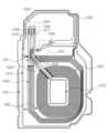
제 1 코일(510) 및 제 3 코일(530)은 제 1 층에 배치될 수 있다. 제 3 코일(530)은 제 1 코일(510)의 외측에 인접할 수 있으며, 이는 제 1 코일(510)의 외측에 배치되는 다음 코일이 제 3 코일(530)이라는 것을 의미할 수 있다. 제 3 코일(530)의 권선 반지름은, 제 1 코일(510)의 권선 반지름보다 클 수 있다. 즉, 제 1 코일(510)은 상대적으로 내측에 배치되며, 제 3 코일(510)은 제 1 코일(510)에 비하여 상대적으로 외측에 배치될 수 있다. 여기에서, 내측 또는 외측은, 코일(510,530)의 중심으로부터의 거리에 따라 결정될 수 있다. 도 5에 도시된 바와 같이, 코일의 중심으로부터 제 1 코일(510)까지의 거리는 코일의 중심으로부터 제 3 코일(530)까지의 거리보다 짧은 수 있으며, 이에 따라 제 1 코일(510)이 제 3 코일(530)에 비하여 상대적으로 내측에 배치된 것으로 명명할 수 있다. 한편, 도시되지는 않았지만, 제 1 층에는 2개보다 많은 수의 코일이 배치될 수도 있다. 즉, 제 3 코일(530)의 외측에는 추가적인 코일들이 더 배치될 수도 있다. 즉, 제 1 층에는 복수 개의 코일(예를 들어, 제 1 코일(510), 제 3 코일(530))이 배치될 수 있다. 여기에서, 복수 개의 코일은, 하나의 동작(예를 들어, MST를 위한 자기장 방출)을 수행할 수 있다. 복수 개의 코일은 전도체와 제 2 층의 복수 개의 코일을 통하여 서로 연결될 수 있다. 더욱 상세하게 후술할 것으로, 제 1 층에는 다른 동작(예를 들어, 무선 충전 또는 NFC 통신 등)을 위한 추가적인 복수 개의 코일들이 더 배치될 수도 있다. 이 경우, 복수 개의 코일과, 추가적인 복수 개의 코일은 서로 직접적으로 연결되지 않을 수 있다.The
제 1 코일(510)은 시작점(511)부터 종점(512)까지 연결되는 전도체를 포함할 수 있으며, 전도체는 권선(winding)된 형태를 가질 수 있다. 도 5의 실시예에서는, 제 1 코일(510)을 구성하는 전도체가 직각으로 구부러져서 권선된 형태를 가지는 것과 같이 도시되어 있지만, 이는 단순히 예시적인 것으로, 제 1 코일(510)은 특정 방향으로 유도 자기장을 방출할 수 있도록 하는 형태의 전도체라면 제한이 없다. 제 1 코일(510)의 시작점(511)은 제 1 코일(510)의 종점(512)보다 실질적으로 내측에 형성될 수 있다. 여기에서, 내측은 제 1 코일(510)의 중심점으로부터 상대적으로 가까운 측을 의미할 수 있다. 제 1 코일(510)에는 전류(i)가 인가될 수 있으며, 인가되는 전류(i)에 따라 제 1 코일(510)은 유도 자기장을 방출할 수 있다. 한편, 제 3 코일(530)에도 제 1 코일(510)과 동일한 방향의 전류(i)가 인가될 수 있으며, 제 3 코일(530) 또한 유도 자기장을 방출할 수 있다. 제 1 코일(510) 및 제 3 코일(530)로부터 방출되는 자기장을 제 1 자기장(B1)으로 명명할 수 있다. The
제 1 코일(510)은 닫힌 루프(closed loop)의 형태를 가질 수 있다. 더욱 상세하게, 제 1 코일(510)의 종점(512)으로부터 연결되는 제 2 연결부(514)는 위에서 내려보았을 때에 우측으로 신장하는 형태를 가질 수 있다. 제 2 연결부(514)는 제 1 코일(510)의 시작점(511)의 x축 방향의 좌표를 통과하여 우측으로 신장할 수 있으며, 이에 따라 제 1 코일(510)의 시작점(511)이 제 2 연결부(514)에 의하여 외부에 대하여 차단될 수 있다. 상술한 바와 같이, 코일의 시작점이 종점과 연결된 연결부에 의하여 외부에 대하여 닫힌 형태를 닫힌 루프의 형태라고 명명하도록 한다. 즉, 닫힌 루프의 형태에서는, 제 1 코일(510)의 종점(512)의 x축 좌표가 제 1 코일의 시작점(511)의 x축 좌표보다 우측에 배치될 수 있다. 한편, 제 1 코일(510) 중 제 1 연결부(513) 및 제 2 연결부(514)는 전도체, 즉 비아 세트와의 연결을 위한 부분일 수 있으며, 연결부(513,514)를 제외한 나머지 부분은 권선을 위한 부분일 수 있다. 이에 따라, 코일 중 연결부를 제외한 나머지 부분을 권선 패턴이라 명명할 수 있다.The
제 1 코일(510)은 전반적으로 d1의 너비를 가질 수 있다. 한편, 제 1 코일(510)의 시작점(511)에 연결되는 제 1 연결부(513)는 전반적으로 d2의 너비를 가질 수 있으며, 이에 따라 제 1 연결부(513)의 일부는 너비가 d1으로부터 d2로 감소하는 형태를 가질 수 있다. 제 1 연결부(513)의 너비(d2)가 제 1 코일(510)의 전반의 너비(d1)보다 짧음에 따라, 복수 개의 전도체(561 내지 564)가 배치될 공간이 확보될 수 있으며, 제 1 층에 배치되는 코일들(510,530)의 전체 실장 면적도 감소할 수 있다. 예를 들어, 만약 제 1 연결부(513)가 d1의 너비를 가지게 되면, 제 1 연결부(513)과 제 2 연결부(514)의 이격을 위하여 해당 부분의 너비가 2×d1을 초과하게 되지만, 제 1 연결부(513)의 너비가 감소하는 구조로 제 1 연결부(513)와 제 2 연결부(514)가 배치되는 부분의 코일 전체 너비가 d1 정도일 수 있다. 더욱 상세하게, 제 1 연결부(513), 제 2 연결부(514) 및 제 1 연결부(513)와 제 2 연결부(514) 사이의 간격이 합이 d1 미만일 수 있다. 이에 따라, 코일의 시작점과 종점이 위치하는 부분의 코일의 실장 면적이 넓어지는 것이 방지될 수 있다.The
본 발명의 다양한 실시예에서, 제 1 연결부(513)의 너비가 좁아지는 구조 및 제 2 연결부(514)의 너비가 좁아지는 구조는 서로 대응될 수 있다. 더욱 상세하게, 제 1 연결부(513)는 위에서 내려다본 경우 좌상측 방향으로 너비가 좁아지는 구조를 가질 수 있으며, 제 2 연결부(514)는 위에서 내려다본 경우 우하측 방향으로 너비가 좁아지는 구조를 가질 수 있다. 즉, 제 1 연결부(513)는 시작점(511)으로부터 권선 패턴의 제 1 측단 방향으로 너비가 증가하는 형태를 가질 수 있고, 제 2 연결부(514)는 종점(512)으로부터 권선 패턴의 제 2 측단 방향으로 너비가 증가하는 형태를 가질 수 있으며, 이는 나머지 코일들에서도 적용될 수 있다. 이에 따라, 제 1 연결부(513) 및 제 2 연결부(514)가 d1의 너비 내에서 함께 배치될 수 있다. 더욱 상세하게, 상기 제 1 연결부(513)의 너비(d2), 상기 제 2 연결부(514)의 너비(d2) 및 상기 제 1 연결부(513) 및 상기 제 2 연결부(514) 사이의 거리의 합계는, 상기 제 1 코일(510)의 권선 패턴의 너비(d1)보다 작을 수 있다.In various embodiments of the present disclosure, a structure in which the width of the
제 1 코일(510)의 종점(512)은 제 1 전도체(561)에 연결될 수 있다. 제 1 전도체(561)는, 예를 들어 제 1 코일(510)이 배치되는 제 1 층와 실질적으로 수직하는 방향으로 형성될 수 있다. 제 1 전도체(561)는 제 2 코일(520)의 시작점(521)과 연결될 수 있다. 즉, 제 1 전도체(561)는 제 1 코일(510)의 종점(512)과 제 2 코일(520)의 시작점(521)을 연결할 수 있으며, 제 1 코일(5210)의 종점(512)으로부터 제 2 코일(520)의 시작점(521)으로 전류(i)가 인가되도록 할 수 있다. 제 1 전도체(561)는 제 1 코일(510)이 배치되는 제 1 층 및 제 2 코일(520)이 배치되는 제 2 층과 실질적으로 수직하는 방향으로 연장될 수 있다. 설명의 편의를 위하여 도시되지는 않았지만, 제 1 층 및 제 2 층 사이에는 다른 구성요소가 배치될 수도 있으며, 이 경우 제 1 전도체(561)는 사이에 배치되는 다른 구성 요소에 형성된 개구를 통하여 두 코일(510,520)을 연결할 수 있다. 이러한 경우, 제 1 전도체(561)를 비아 세트(via set)라고 명명할 수도 있다. 본 발명의 다양한 실시예에서, 도 5에서의 하나의 전도체는, 복수 개의 분리된 전도체로 구현될 수도 있다. 즉, 제 1 코일(510)의 종점(512)과 제 2 코일(520)의 시작점(521)을 복수 개의 분리된 전도체들이 수직 방향으로 연결할 수 있다. 결국, 제 1 층의 코일의 종점과, 제 2 층의 코일의 시작점을 연결하는 전도체의 개수는 하나 또는 이상으로 구현될 수 있으며, 이에 따라 전도체가 비아 세트로 명명될 수도 있다.The
한편, 제 1 층 및 제 2 층에 배치된다는 것은, PCB(printed circuit board) 또는 FPCB(flexible printed circuit board)의 두 개에 각각 배치되는 것일 수 있다. 또는, 하나의 PCB 또는 FPCB의 양면 각각에 제 1 코일(510) 및 제 2 코일(520) 각각이 배치될 수도 있다. 이 경우에는, 전도체, 즉 비아 세트가 하나의 PCB 또는 FPCB를 통과하는 구조로 형성될 수도 있다. 이때에는, 제 1 코일(510)은 제 1 층에 배치되며, 제 2 코일(520)은 제 2 층에 배치된다고 명명될 수도 있다. 또는, 두 개의 층의 코일이 FPCB의 내측에 배치되며, 해당 코일을 보호하기 위한 도금층 또는 필름 등이 추가적으로 FPCB에 포함될 수도 있으며, 이는 더욱 상세하게 후술하도록 한다. 아울러, 제 1 층 및 제 2 층은 실질적으로 평행할 수 있다.Meanwhile, being disposed on the first layer and the second layer may mean being disposed on two of a printed circuit board (PCB) or a flexible printed circuit board (FPCB), respectively. Alternatively, each of the
제 2 코일(520)은 제 1 전도체(561)를 통하여 전류(i)를 수신할 수 있다. 이 경우, 전류(i)는 제 2 코일(520)의 시작점(521)으로부터 제 2 코일(520)의 종점(522) 방향으로 인가될 수 있으며, 종점(522)과 연결된 제 2 전도체(562)로 인가될 수 있다. 제 2 코일(520)은 인가되는 전류(i)에 기초하여 유도 자기장을 방출할 수 있다. 제 2 코일(520) 및 제 4 코일(540)이 방출하는 유도 자기장을 제 2 자기장(B2)으로 명명할 수 있다.The
제 2 코일(520)은 시작점(521)으로부터 종점(522)까지 연결되는 전도체를 포함하며, 전도체는 시작점(521)으로부터 종점(522)까지 권선된 형태를 가질 수 있다. 제 2 코일(520)은 시작점(521)에 연결되는 제 3 연결부(523) 및 종점(522)에 연결되는 제 4 연결부(524)를 포함할 수 있다. 제 3 연결부(523) 및 제 4 연결부(524)의 전반적인 너비는, 제 2 코일(520)의 전반적인 너비에 비하여 작을 수 있다. 아울러, 제 1 코일(510)의 연결부(513,514)에 대하여 설명한 바와 같이, 연결부(523,524)의 일부는 제 2 코일(520)의 전반적인 너비, 즉 권선 패턴의 너비(d1)로부터 너비가 감소하는 형태를 가질 수도 있다.The
제 2 코일(520)은 열린 루프(opened loop)의 형태, 즉 개방된 형태를 가질 수 있다. 더욱 상세하게, 제 2 코일(520)의 종점(522)으로부터 연결되는 제 4 연결부(524)는 위에서 내려보았을 때에 우측으로 신장하는 형태를 가질 수 있다. 제 4 연결부(524)는 제 2 코일(520)의 시작점(521)의 x축 방향의 좌표를 통과하지 않도록 신장할 수 있으며, 이에 따라 제 2 코일(520)의 시작점(521)이 제 4 연결부(524)에 의하여 외부에 대하여 닫힐 수 없다. 즉, 제 2 코일(520)의 종점(522)의 x축 좌표는 제 2 코일(520)의 시작점(521)의 x축 좌표에 비하여 상대적으로 좌측에 위치할 수 있다. 상술한 바와 같이, 코일의 시작점이 종점과 연결된 연결부에 의하여 외부에 대하여 닫히지 않는 형태를 열린 루프의 형태라고 명명하도록 한다. 한편, 더욱 상세하게 후술할 것으로, 제 2 코일(520)이 열린 루프의 형태를 가짐에 따라서, 제 2 코일(520)의 내측에 다른 코일이 배치되면서, 다른 코일의 입/출력 패턴이 제 2 코일(520)의 열린 루프의 간격에 배치될 수 있다.The
한편, 제 2 코일(520)의 종점(522)은 제 2 전도체(562)에 연결될 수 있다. 제 2 전도체(562)는 제 1 층에 배치되는 제 3 코일(530)의 시작점(531)에 연결될 수 있다. 이에 따라, 제 2 코일(520)의 종점(522)은 제 3 코일(530)의 시작점(531)에 연결될 수 있다. 제 2 코일(520)의 종점(522)으로부터 제 3 코일(530)의 시작점(531)으로 전류(i)가 인가됨에 따라서, 제 2 전도체(562)에 인가되는 전류(i)의 방향은 상측 방향일 수 있다.Meanwhile, the
제 3 코일(530)은 제 2 전도체(562)를 통하여 전류(i)를 수신할 수 있다. 이 경우, 전류(i)는 제 3 코일(530)의 시작점(531)으로부터 제 3 코일(530)의 종점(532) 방향으로 인가될 수 있으며, 종점(532)과 연결된 제 3 전도체(563)로 인가될 수 있다. 제 3 코일(530)은 인가되는 전류(i)에 기초하여 유도 자기장을 방출할 수 있다.The
제 3 코일(530)은 시작점(531)으로부터 종점(532)까지 연결되는 전도체를 포함하며, 전도체는 시작점(531)으로부터 종점(532)까지 권선된 형태를 가질 수 있다. 제 3 코일(530)은 시작점(531)에 연결되는 제 5 연결부(533) 및 종점(532)에 연결되는 제 6 연결부(534)를 포함할 수 있다. 제 5 연결부(533) 및 제 6 연결부(534)의 전반적인 너비는, 제 3 코일(530)의 전반적인 너비에 비하여 작을 수 있다. 아울러, 제 1 코일(510)의 연결부(513,514)에 대하여 설명한 바와 같이, 연결부(533,534)의 일부는 제 3 코일(530)의 전반적인 너비(d1)로부터 너비가 감소하는 형태를 가질 수도 있다. 제 3 코일(530)은 닫힌 루프의 형태를 가질 수 있다.The
한편, 제 3 코일(530)의 종점(532)은 제 3 전도체(563)에 연결될 수 있다. 제 3 전도체(563)는 제 2 층에 배치되는 제 4 코일(540)의 시작점(541)에 연결될 수 있다. 이에 따라, 제 3 코일(530)의 종점(532)은 제 4 코일(540)의 시작점(541)에 연결될 수 있다. 제 3 코일(530)의 종점(532)으로부터 제 4 코일(540)의 시작점(541)으로 전류(i)가 인가됨에 따라서, 제 3 전도체(563)에 인가되는 전류(i)의 방향은 하측 방향일 수 있다.Meanwhile, the
제 4 코일(540)은 제 3 전도체(563)를 통하여 전류(i)를 수신할 수 있다. 이 경우, 전류(i)는 제 4 코일(540)의 시작점(541)으로부터 제 4 코일(540)의 종점(542) 방향으로 인가될 수 있으며, 종점(542)과 연결된 출력단으로 인가될 수 있다. 제 4 코일(540)은 인가되는 전류(i)에 기초하여 유도 자기장을 방출할 수 있다.The
제 4 코일(540)은 시작점(541)으로부터 종점(542)까지 연결되는 전도체를 포함하며, 전도체는 시작점(541)으로부터 종점(542)까지 권선된 형태를 가질 수 있다. 제 4 코일(540)은 시작점(541)에 연결되는 제 7 연결부(543)를 포함할 수 있다. 제 7 연결부(543)의 전반적인 너비는, 제 4 코일(540)의 전반적인 너비, 즉 권선 패턴의 너비에 비하여 작을 수 있다. 아울러, 제 1 코일(510)의 연결부(513,514)에 대하여 설명한 바와 같이, 연결부(543)의 일부는 제 4 코일(540)의 전반적인 너비(d1)로부터 너비가 감소하는 형태를 가질 수도 있다. 제 4 코일(530)은 열린 루프의 형태를 가질 수 있다.The
한편, 제 2 층에는 입력 패턴(550)이 배치될 수 있다. 입력 패턴(550)은 제 4 전도체(564)와 연결될 수 있으며, 제 4 전도체(564)는 제 1 코일(511)의 시작점(511)에 연결될 수 있다. 입력 패턴(550)은 전류를 제공할 수 있는 수단(예를 들어, MST 통신 모듈, 통신 모듈, 또는 배터리 또는 PMIC)에 연결될 수 있으며, 이에 따라 전류(i)가 입력 패턴(550)으로부터 제 1 코일(510)로 인가될 수 있다. 제 4 전도체(564)에 인가되는 전류(i)의 방향은 상측 방향일 수 있다.Meanwhile, the
결국, 전류가 인가되는 코일의 순서, 또는 코일의 연결 순서는 C11, C21, C12, C22, C13, C23, …의 순서일 수 있다. 여기에서, Cij에서의 i는 층을 의미할 수 있으며, j는 내측으로부터 배치되는 순서일 수 있다. 예를 들어, C21은 제 2 층의 내측으로부터 첫번째 코일을 의미할 수 있으며, C32는 제 3 층의 내측으로부터 두번째 코일을 의미할 수 있다.After all, the order of coils to which current is applied, or the order of connecting coils, is C11 , C21 , C12 , C22 , C13 , C23 , . . . can be in the order of Here, i in Cij may mean a layer, and j may be an arrangement order from the inside. For example, C21 may mean a first coil from the inside of the second layer, and C32 may mean a second coil from the inside of the third layer.
상술한 코일 구조에 따라서, 입력 패턴(550)으로부터 제공되는 전류(i)는 제 1 코일(510), 제 2 코일(520), 제 3 코일(530) 및 제 4 코일(540)에 인가될 수 있다. 이에 따라, 코일 전체의 권선 회수가 증가할 수 있어, 코일의 인덕턴스 또한 증가할 수 있다. 즉, 2회의 권선이 가능한 실장면적에, 4회의 권선이 가능할 수 있으므로 코일의 인덕턴스가 증가할 수 있다. 결국, 코일에 의하여 방출되는 자기장(B1+B2)의 크기 또한 증가할 수 있다. 뿐만 아니라, 전도체(561 내지 564)에 의하여 방출되는 자기장(B3) 또한 형성될 수 있어, 전체 자기장의 세기가 증가할 수 있다. 특히, 전류의 방향이 동일한 전도체끼리 그룹핑되어 배치됨에 따라, 전도체(561 내지 564)에 의하여 방출되는 자기장(B3)이 증가할 수 있다. 뿐만 아니라, 전류의 방향이 동일한 전도체들의 배열 형태(예를 들어, 일직성 형태)에 따라, 전도체에 의하여 방출되는 지향성 자기장의 방향이 결정될 수 있다. 이에 따라, 지향성 자기장의 방향을 고려하여, 전류의 방향이 동일한 전도체들의 배열 형태가 결정될 수도 있다. 더욱 상세하게, 인가되는 전류가 상측 방향인 전도체들(562,564)이 서로 인접하도록 배치되며, 인가되는 전류가 하측 방향인 전도체들(561,563)이 서로 인접하게 배치될 수 있다. 아울러, 전도체(561 내지 564)에 의하여 방출되는 자기장(B3)의 방향은 코일(510 내지 540)에 의하여 방출되는 자기장(B1+B2)의 방향과 상이할 수 있어, 전자 장치(101)는 다양한 방향으로 자기장을 방출할 수 있다. 이에 따라, 전자 장치(101)의 배치에 대한 자유도가 증가할 수 있으며, 이에 대하여서는 더욱 상세하게 후술하도록 한다.According to the coil structure described above, the current i provided from the
도 6a는 본 발명의 다양한 실시예에 의한 제 1 층에 배치되는 코일의 평면도를 도시한다. 도 6b는 본 발명의 다양한 실시예에 의한 제 2 층에 배치되는 코일의 평면도를 도시한다. 도 6c는 제 1 층 및 제 2 층에 배치되는 코일을 겹쳐지도록 구성한 평면도를 도시한다.6A shows a plan view of a coil disposed in a first layer in accordance with various embodiments of the present invention. 6B illustrates a top view of a coil disposed in a second layer according to various embodiments of the present invention. FIG. 6C is a plan view in which coils disposed on the first layer and the second layer are overlapped.
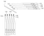
제 1 층에는 제 1 코일(510) 및 제 3 코일(530)이 배치될 수 있다. 제 3 코일(530)은 제 1 코일(510)의 외측에 인접할 수 있다. 제 1 코일(510) 및 제 3 코일(530)은 닫힌 루프 형태를 가질 수 있다. 한편, 제 2 층에는 제 2 코일(520) 및 제 4 코일(540)이 배치될 수 있다. 제 4 코일(540)은 제 2 코일(510)의 외측에 인접할 수 있다. 제 2 코일(520) 및 제 4 코일(540)은 열린 루프 형태를 가질 수 있다. 한편, 도 6c에 도시된 바와 같이, 제 1 코일(510)에서 제 1 연결부(513) 및 제 2 연결부(514)를 제외한 부분과, 제 2 코일(520)에서 제 3 연결부(523) 및 제 4 연결부(524)를 제외한 부분이 겹쳐질 수 있다. 이는, 위에서 바라본 경우, 제 1 코일(510)에서 제 1 연결부(513) 및 제 2 연결부(514)를 제외한 부분의 위치와 제 2 코일(520)에서 제 3 연결부(523) 및 제 4 연결부(524)를 제외한 부분, 즉 권선 패턴의 위치가 실질적으로 동일함을 의미할 수 있다. 한편, 상술한 바와 같은 코일의 배치는 단순히 예시적인 것으로, 제 1 코일(510) 및 제 2 코일(520)은 서로 겹쳐지지 않도록 구성될 수도 있다. 본 발명의 다양한 실시예에서, 제 3 코일(530) 및 제 4 코일(540) 또한 연결부를 제외한 대부분, 즉 권선 패턴들이 서로 겹쳐지도록 배치될 수도 있다.A
제 1 코일(510)의 제 1 연결부(513)와 제 2 코일(520)의 제 2 연결부(523)는 서로 겹쳐지지 않을 수 있다. 이는, 제 1 코일(510)의 종점(512)이 제 2 코일(520)의 시작점(521)과 연결되어야 하므로, 제 1 코일(510)의 제 2 연결부(514)가 제 2 코일(520)의 시작점(521)까지 연장되어야 하는 것으로부터 기인할 수 있다. 이에 따라, 본 발명의 다양한 실시예에서, 제 1 코일(510) 및 제 2 코일(520)은 각각의 연결부를 제외한 부분, 즉 권선 패턴이 서로 겹치도록 배치될 수 있으며, 연결부는 겹치지 않도록 배치될 수 있다.The
한편, 도 6c에서 도시된 바와 같이, 인가되는 전류가 상측 방향인 전도체들(562,564)이 서로 인접하도록 배치되며, 인가되는 전류가 하측 방향인 전도체들(561,563)이 서로 인접하게 배치될 수 있다. 도 7은 본 발명의 다양한 실시예에 따른 전도체의 위치를 설명하기 위한 평면도를 도시한다. 도 7에 도시된 바와 같이, 제 2 전도체(562) 및 제 4 전도체(564) 사이의 거리(X1)는, 제 2 전도체(562) 및 제 1 전도체(561) 사이의 거리(X2) 또는 제 2 전도체(562) 및 제 3 전도체(563) 사이의 거리(X3)보다 상대적으로 작을 수 있다. 아울러, 제 1 전도체(561) 및 제 3 전도체(563) 사이의 거리(X4)는, 제 2 전도체(562) 및 제 1 전도체(561) 사이의 거리(X2) 또는 제 2 전도체(562) 및 제 3 전도체(563) 사이의 거리(X3)보다 상대적으로 작을 수 있다. 즉, 인가되는 전류가 동일한 방향의 전도체들끼리 서로 인접하도록 전도체(561 내지 564)의 패턴이 설계될 수 있다. 이에 따라, 제 2 전도체(562) 및 제 4 전도체(564)로부터 방출되는 유도 자기장(B4)의 방향과 제 1 전도체(561) 및 제 3 전도체(563)로부터 방출되는 유도 자기장(B5)의 방향이 제 1 전도체(561) 및 제 2 전도체(562) 사이에서 동일할 수 있다. 유도 자기장(B4,B5)의 벡터합은 도 5에서 설명한 전도체들(561 내지 564)에 의한 제 3 자기장(B3)일 수 있다. 전도체들(561 내지 564)에 의한 제 3 자기장(B3)은 일반적인 단독 도선에 의하여 형성되는 원형 자기장과는 상이한 특정한 방향을 가리키는 지향성을 가질 수 있다. 한편, 도 7에서 제 2 전도체(562) 및 제 4 전도체(564)를 이은 직선은 제 1 방향을 가질 수 있으며, 제 1 전도체(561) 및 제 3 전도체(563)을 이은 직선은 제 2 방향을 가질 수 있다. 제 1 방향 및 제 2 방향은 동일할 수도 있거나 상이할 수도 있다. 제 1 방향 및 제 2 방향에 따라, 제 3 자기장(B3)의 방향이 결정될 수 있다. 제작자는, 사용자가 전자 장치를 POS 단말기 근처에 위치시키는 패턴을 고려하여, 제 1 방향 및 제 2 방향을 결정할 수도 있다.Meanwhile, as shown in FIG. 6C ,
도 8a 및 8b는 본 발명의 다양한 실시예에 따른 전자 장치의 배치의 자유도 증가를 설명하기 위한 개념도를 도시한다.8A and 8B are conceptual diagrams for explaining an increase in the degree of freedom of arrangement of electronic devices according to various embodiments of the present disclosure.
도 8a를 참조하면, 전자 장치(101)는 디스플레이에 실질적으로 수직한 방향으로 자기장(B1+B2)을 방출할 수 있다. 이에 따라, 전자 장치(101)의 디스플레이가 포스 단말기(301)와 상대적으로 평행하게 배치된 경우에는 방출되는 자기장(B1+B2)이 포스 단말기(301)로 향할 수 있어, MST 신호의 양호한 전송이 가능할 수 있다. 한편, 도 8b를 참조하면, 전자 장치(101)는 디스플레이에 실질적으로 평행한 방향으로 자기장(B3)을 방출할 수 있으며, 이는 코일 연결을 위한 전도체, 즉 비아 세트에 인가되는 전류에 의하여 유도될 수 있다. 이에 따라, 전자 장치(101)의 디스플레이가 포스 단말기(301)와 상대적으로 수직하게 배치된 경우에도, 방출되는 자기장(B3)이 포스 단말기(301)로 향할 수 있어, MST 신호의 양호한 전송이 보장될 수 있다. 이에 따라, 전자 장치(101)의 배치가 포스 단말기(301) 기준으로 비교적 자유로울 수 있다.Referring to FIG. 8A , the
도 9a는 본 발명의 다양한 실시예에 따른 제 2 층에 배치되는 코일을 설명하기 위한 평면도를 도시한다.9A is a plan view illustrating a coil disposed on a second layer according to various embodiments of the present disclosure.
도 9a에 도시된 바와 같이, 제 2 층에는 오픈 루프 형태를 가지는 제 2 코일(520) 및 제 4 코일(540)이 배치될 수 있다. 한편, 제 2 코일(520)에는 입력 패턴(550)이 배치될 수 있다. 제 2 코일(520)이 오픈 루프 형태를 가짐에 따라서, 제 2 코일(520)의 시작점(521) 및 제 2 코일(520)의 종점(522) 사이의 간격이 생길 수 있다. 아울러, 입력 패턴(550) 및 제 2 코일(520) 사이에도 간격(901)이 생길 수 있다. 입력 패턴(550) 및 제 2 코일(520) 사이에 간격(901)이 생김에 따라서, 제 2 층에는 추가적인 코일(910)이 더 배치될 수 있다. 예를 들어, 추가적인 코일(910)은 l1의 너비를 가질 수 있으며, 간격(901)은 l1의 두 배를 넘을 수 있다. 이에 따라, 추가적인 코일(910)이 제 2 코일(520) 내에 배치되도록 입력되는 부분과 출력되는 부분, 즉 입/출력 패턴이 간격(901) 내에서 함께 배치될 수 있다. 추가적인 코일(910)은 코일들(510 내지 540)과 동일한 목적을 위한 것일 수도 있으며, 또는 상이한 목적을 위한 것일 수도 있다. 예를 들어, 코일들(510 내지 540)이 MST를 위한 것인 경우에, 추가적인 코일(910) 또한 널(null) 영역의 보충을 위한 MST용 코일일 수도 있으며, 이에 대하여서는 더욱 상세하게 후술하도록 한다. 또는, 추가적인 코일(910)은 무선 충전을 위한 코일이거나 또는 다른 방식의 통신(예를 들어, NFC 통신)을 위한 것일 수도 있다.As shown in FIG. 9A , the
즉, 상술한 바와 같이 적어도 하나의 층에 배치되는 코일들이 오픈 루프 형태를 가짐에 따라서, 오픈 루프 형태의 코일 내에 또 다른 추가적인 코일이 배치될 수 있다.That is, as the coils disposed on at least one layer have an open loop shape as described above, another additional coil may be disposed within the open loop coil.
도 9b는 본 발명의 다양한 실시예에 따른 추가 코일까지 배치된 구조를 설명하는 사시도를 도시한다.9B is a perspective view illustrating a structure in which an additional coil is disposed according to various embodiments of the present disclosure.
도 9b에 도시된 바와 같이, 제 1 추가 코일(921,922)이, 본 발명의 실시예에 다른 코일(911,912)의 내측에 배치될 수 있다. 상술한 바와 같이, 코일(912)는 열린 루프 형태를 가질 수 있으며, 이에 따라 제 1 추가 코일(921,922)에 대응하는 입/출력 패턴(925,926)이 코일(912)의 열린 루프 형태에 따른 간격에 배치될 수 있다. 한편, 제 1 추가 코일(921,922)은 전도체, 즉 비아 세트(923,924)를 통하여 수직 방향으로 연결될 수 있다. 아울러, 코일(911,912) 또한 비아 세트들(913,914)를 통하여 수직 방향으로 연결될 수 있다. 한편, 코일(911,912)의 외측에는 제 2 추가 코일(931,932)이 배치될 수 있으며, 제 2 추가 코일(931,931)은 비아 세트 (933,934)를 통하여 수직 방향으로 연결될 수 있다. 도 9b에서, 제 1 추가 코일(921,922) 및 제 2 추가 코일(931,932) 각각은 서브 코일들이 서로 병렬로 연결되는 것과 같이 도시되어 있지만, 이는 단순히 예시적인 것으로, 제 1 추가 코일(921,922) 및 제 2 추가 코일(931,932)에서도 역시, 도 5와 같은 구조로 서브 코일들이 서로 직렬로 연결될 수도 있다.As shown in FIG. 9B , the first
도 10a는 본 발명의 다양한 실시예에 따른 다양한 목적의 복수 개의 코일들이 배치되는 제 1 층의 평면도를 도시한다. 제 1 층에는 MST용 코일(1020)이 배치될 수 있다. 예를 들어, MST용 코일(1020)은 제 1 층에서 5회의 권선 회수로 권선된 형태를 가질 수 있으며, 닫힌 루프 구조를 가질 수 있다. 도 10a에 도시된 바와 같이, MST용 코일(1020)의 각 시작점들은 종점에 연결되는 연결부(1021)에 의하여 외부에 대하여 닫힌 구조일 수 있다. MST용 코일(1020)은 전도체, 즉 비아 세트를 통하여 제 2 층의 MST용 코일(1050)과 연결될 수 있다.10A is a plan view of a first layer in which a plurality of coils for various purposes are disposed according to various embodiments of the present invention. A
한편, 제 1 층에는 추가적인 MST용 패턴(1024)이 배치될 수 있으며, 입력 단자 및 출력 단자와 MST용 패턴(1024) 또는 MST용 코일(1020)을 연결하기 위한 MST용 입/출력 패턴(1025,1026)이 더 배치될 수도 있다.Meanwhile, an
제 1 층에는, NFC용 코일(1010)이 배치될 수 있다. 아울러, NFC용 코일(1010)과 입/출력 단자를 연결하기 위한 NFC용 입/출력 패턴(1012,1013)이 배치될 수 있다. NFC용 코일(1010)은 MST용 코일(1020)의 외측에 배치될 수 있다.In the first layer, a
MST용 코일(1020)의 내측에는 무선 충전용 코일(1030)이 배치될 수 있다. 무선 충전용 코일(1030)은 유도 방식(예를 들어, WPC 표준 방식) 또는 공진 방식(예를 들어, A4WP 표준 방식)에서 정의된 공진 주파수를 가지도록 제작될 수 있다. 한편, 무선 충전용 코일(1030)의 내측에는 NFC용 코일(1011)이 추가적으로 배치될 수도 있다. 한편, 제 1 층에는, 온도측정회로용 입/출력 단자 연결부(1041,1042)가 더 배치될 수 있다. 제 1 층에는 더미 패턴(dummy pattern)(1001)이 배치될 수 있다. 아울러, NFC용 코일(1010)과 MST용 코일(1020) 사이의 이격 및 MST용 코일(1020)과 무선 충전용 코일(1030) 사이의 이격을 위하여 간격(1002)이 설정될 수도 있다. 더미 패턴(1101)은 얇은 두께의 코일 FPCB의 강성을 보완하여, 각 코일에서 발생될 수 있는 크랙(crack)을 방지할 수 있다. 간격(1002)은 하나의 코일이 다른 코일에 미치는 영향을 감소시키기 위한 것일 수 있다. 한편, NFC용 코일(1010) 및 무선 충전용 코일(1030) 또한 전도체, 즉 비아 세트를 통하여 직렬로 연결되는 복수 개의 서브 코일을 포함하는 구조로 구현될 수도 있다.A
도 10b는 본 발명의 다양한 실시예에 따른 다양한 목적의 복수 개의 코일들이 배치되는 제 2 층의 평면도를 도시한다. 제 2 층에는 MST용 코일(1050)이 배치될 수 있다. 제 2 층의 MST용 코일(1050)은 전도체, 즉 비아 세트를 통하여 제 1 층의 MST용 코일(1020)과 수직 방향으로 연결될 수 있다. 제 2 층에는 MST용 입/출력 단자(1053,1054)가 배치될 수 있다. MST용 입/출력 단자(1053,1054)를 통하여, MST용 코일(1020,1050)과 MST용 패턴(1024,1052,1055)으로 전류가 인가된 후 출력될 수 있다. MST용 코일(1050)의 연결부(1051)는 다른 쪽 말단을 외부를 향하여 닫지 못하며, MST용 코일(1050)은 열린 루프 형태를 가질 수 있다. MST용 코일(1050)이 열린 루프 형태를 가짐에 따라서, MST용 코일(1050)의 간격을 통하여 무선 충전용 코일(1031)이 입/출력 단자와 연결될 수 있다. 더욱 상세하게, 무선 충전용 입/출력 패턴(1032,1033)이 MST용 코일(1050)의 간격 사이에 배치될 수 있다. 입/출력 단자는, C-클립(C-CLIP)과 같은 연결부에 의하여 PCB의 패턴들과 연결될 수 있다. 입/출력 단자는, 통신 모듈로부터 전송되는 음/양(plus/minus)의 펄스(pulse) 위상 변화에 따라 서로 교체될 수 있다. 예를 들어, 하나의 단자는, 음 위상에 대하여서는 입력 단자로 동작하고, 양의 위상에 대하여서는 출력 단자로 동작할 수 있다.10B is a plan view of a second layer in which a plurality of coils for various purposes are disposed according to various embodiments of the present invention. A
무선 충전용 코일(1031)은 전도체, 즉 비아 세트를 통하여 제 1 층에 배치되는 무선 충전용 코일(1030)과 연결될 수 있다. 아울러, 무선 충전용 코일(1031)은 외부의 자기장 또는 전자기장에 대응하는 전류를 출력함으로써 무선 충전을 수행할 수 있다. 또는, 무선 충전용 코일(1031)은 인가되는 전류를 이용하여 자기장을 방출하거나 또는 다른 코일과 함께 공진 회로를 형성하여 전자기장을 방출함으로써 다른 전자 장치를 무선 충전할 수도 있다. 무선 충전용 코일(1031)은 MST용 코일(1050)의 내측에 배치될 수 있다.The
제 2 층에는, NFC용 코일(1012)이 배치될 수 있다. NFC용 코일(1012)은 전도체, 즉 비아 세트를 통하여 제 1 층의 NFC용 코일(1010)과 연결될 수 있다. 제 2 층에는, NFC용 패턴(1013,1014) 또한 배치될 수 있으며, NFC용 패턴(1013,1014) 또한 전도체, 즉 비아 세트를 통하여 제 1 층의 NFC용 코일(1010) 또는 NFC용 입/출력 패턴(1012,1013)과 수직 방향으로 연결될 수 있다. NFC용 입/출력 단자(1016,1017)는 전도체, 즉 비아 세트를 통하여 NFC용 입/출력 패턴(1012,1013)과 수직 방향으로 연결될 수 있으며, 이에 따라 NFC용 입/출력 패턴(1012,1013)과 NFC용 코일(1010,1011,1012,1015)이 연결될 수 있다. NFC용 코일(1015)은 MST용 코일(1050)의 내측에 배치될 수 있으며, MST용 코일(1050)이 열린 루프 형태를 가짐에 따라서 NFC용 패턴(1018)과 연결될 수 있다. 제 2 층에는, 제 1 층의 온도측정회로용 입/출력 단자 연결부(1041,1042)와 전도체, 즉 비아 세트를 통하여 수직 방향으로 연결되는 온도 측정회로(1040) 및 온도 측정회로용 입출력 단자(1043,1044)가 배치될 수 있다. 온도 측정회로(1040)는 각 코일에 전류가 인가되는 경우, 발생할 수 있는 열에 의한 온도를 측정하여 프로세서로 전달할 수 있으며, 프로세서는 전달받은 온도에 기초하여 인가하는 전류의 크기를 조정할 수 있다. 이에 따라, 코일들이 과열되는 것이 방지될 수 있다.In the second layer, a
상술한 바와 같이, 본 발명의 다양한 실시예에서, MST용 코일과 무선 충전용 코일, NFC용 코일 등의 다양한 코일들 각각이 전도체, 즉 비아 세트를 통하여 수직 방향으로 복수 코일이 연결된 구조를 가짐으로써, 각 코일의 인덕턴스가 증가하여 무선 충전 효율 또는 신호의 양호한 송수신이 가능할 수 있다.As described above, in various embodiments of the present invention, each of various coils such as a coil for MST, a coil for wireless charging, and a coil for NFC has a structure in which a plurality of coils are connected in a vertical direction through a conductor, that is, a set of vias. , the inductance of each coil may be increased to enable wireless charging efficiency or good transmission and reception of signals.
도 10c는, 도 10a의 제 1 층의 구조 및 도 10b의 제 2 층의 구조를 겹치도록 구성한 평면도이다. 도 10c에서 "·"의 표시는 전도체, 즉 비아 세트를 의미할 수 있으며, "·"이 표시된 지점에 전도체가 배치되어 제 1 층 및 제 2 층의 대응 구조를 연결할 수 있다. 도 10c에 도시된 바와 같이, 제 1 층에 배치되는 MST용 코일과 제 2 층에 배치되는 MST용 코일은, 연결부(1021,1051)를 제외한 나머지 대부분에서 서로 겹치는 구조를 가질 수 있다. 연결부(1021,1051)에서의 중첩 관계는 도 11a 내지 11c를 참조하여 더욱 상세하게 설명하도록 한다. 한편, 제 1 층의 패턴과 제 2 층의 패턴의 대부분의 영역이 서로 겹치는 구조는 단순히 예시적인 것으로, 본 발명의 다양한 실시예에 의한 전자 장치는 제 1 층의 패턴과 제 2 층의 패턴이 서로 겹치지 않도록 하는 구조를 가질 수도 있다.Fig. 10C is a plan view in which the structure of the first layer of Fig. 10A and the structure of the second layer of Fig. 10B are overlapped. In FIG. 10C , a “·” mark may indicate a conductor, that is, a set of vias, and a conductor may be disposed at a point marked “·” to connect corresponding structures of the first layer and the second layer. As shown in FIG. 10C , the coils for MST disposed on the first layer and the coils for MST disposed on the second layer may have a structure overlapping each other in most parts except for the connecting
도 11a 내지 11c는 본 발명의 다양한 실시예에 의한 코일의 연결부에서의 연결 관계를 설명하기 위한 개념도를 도시한다. 도 11a는 제 1 층에 배치되는 코일의 일부의 평면도를 도시한다.11A to 11C are conceptual diagrams for explaining a connection relationship in a connection unit of a coil according to various embodiments of the present disclosure. 11A shows a plan view of a portion of a coil disposed in the first layer.
도 11a를 참조하면, 제 1 층에는 닫힌 루프 형태를 가지는 코일이 배치될 수 있다. 예를 들어, 제 1 코일(1101), 제 3 코일(1103), 제 5 코일(1105), 제 7 코일(1107) 및 제 9 코일(1109)이 제 1 층에 배치될 수 있다. 제 1 코일(1101)은 제 1 연결부(1102) 및 제 2 연결부(1111)를 포함할 수 있다. 도 11a에서는, 코일의 특정 부분만을 도시함에 따라서, 제 1 연결부(1102) 및 제 2 연결부(1111)가 연결되지 않은 분리된 하드웨어와 같이 도시되어 있지만, 제 1 연결부(1102) 및 제 2 연결부(1111)는 제 1 코일(1101)을 구성하며 서로 연결되어 있다. 한편, 제 1 코일(1101)의 외측에는 제 3 코일(1103)이 배치될 수 있다. 제 3 코일(1103) 제 5 연결부(1104) 및 제 6 연결부(1112)를 포함할 수 있다. 제 3 코일(1103)의 외측에는 제 5 코일(1105)이 배치될 수 있다. 제 5 코일(1105)은 제 9 연결부(1106) 및 제 10 연결부(1113)를 포함할 수 있다. 제 5 코일(1105)의 외측에는 제 7 코일(1107)이 배치될 수 있다. 제 7 코일(1107)은 제 13 연결부(1108) 및 제 14 연결부(1114)를 포함할 수 있다. 제 7 코일(1107)의 외측에는 제 9 코일(1109)이 배치될 수 있다. 제 9 코일(1109)은 제 17 연결부(1110) 및 제 18 연결부(1115)를 포함할 수 있다.Referring to FIG. 11A , a coil having a closed loop shape may be disposed on the first layer. For example, the
제 1 연결부(1102), 제 5 연결부(1104), 제 9 연결부(1106), 제 13 연결부(1108) 및 제 17 연결부(1110)는 권선 패턴에 비하여 작은 너비를 가질 수 있으며, 권선 패턴으로부터 권선 패턴의 상측단 방향으로 너비가 감소하는 형태를 가질 수 있다. 한편, 제 2 연결부(1111), 제 6 연결부(1112), 제 10 연결부(1113), 제 14 연결부(1114) 및 제 18 연결부(1115)는 권선 패턴으로부터 하측단 방향으로 너비가 감소하는 형태를 가질 수 있다. 이에 따라, 예를 들어, 제 5 연결부(1104)와 제 6 연결부(1112)는 서로 겹치지 않는 구조를 가질 수 있으며, 두 연결부(1104,1112)가 하나의 권선 패턴의 너비 내에 함께 배치될 수 있다. 아울러, 연결부를 제외한 나머지 권선 패턴에서는 충분히 두꺼운 너비가 확보됨에 따라, 저항이 감소하여 인가되는 전류의 세기가 커질 수 있다.The
도 11a 및 11c를 참조하면, 제 2 연결부(1111), 제 6 연결부(1112), 제 10 연결부(1113), 제 14 연결부(1114) 및 제 18 연결부(1115)에는 전도체, 즉 비아 세트가 형성될 수 있다. 예를 들어, 제 6 연결부(1112)에 연결되는 전도체는, 제 6 연결부(1112)와 제 2 층의 제 2 코일(1127)을 연결할 수 있다. 더욱 상세하게는, 제 4 연결부(1112)의 전도체는, 제 6 연결부(1112)와 제 2 코일(1127)의 제 3 연결부(1128)를 수직 방향으로 연결할 수 있다. 아울러, 제 10 연결부(1113)의 전도체는, 제 10 연결부(1113)와 제 4 코일(1125)의 제 7 연결부(1126)를 수직 방향으로 연결할 수 있다. 제 14 연결부(1114)의 전도체는, 제 14 연결부(1114)와 제 6 코일(1123)의 제 11 연결부(1124)를 수직 방향으로 연결할 수 있다. 제 18 연결부(1115)의 전도체는, 제 18 연결부(1115)와 제 8 코일(1121)의 제 15 연결부(1122)를 수직 방향으로 연결할 수 있다.11A and 11C, the
도 11b 및 11c를 참조하면, 제 2 연결부(1111)는 입력 패턴(1140)으로부터 전류를 인가받을 수 있으며, 전류는 제 1 코일(1101)에 인가되고, 제 1 연결부(1101)에 연결되는 전도체를 따라 제 4 연결부(1131)를 통하여 제 2 코일(1127)로 인가될 수 있다. 제 4 연결부(1131)의 전도체는, 제 4 연결부(1131)와 제 1 연결부(1102)를 수직 방향으로 연결할 수 있다. 한편, 제 4 연결부(1131)로부터 인가되는 전류는 제 2 코일(1127)에 인가된 이후에 제 3 연결부(1128)로 전달될 수 있다. 제 7 연결부(1128)의 전도체는, 제 3 연결부(1128)와 제 3 코일(1103)의 제 6 연결부(1112)를 수직 방향으로 연결할 수 있다. 이에 따라, 제 3 연결부(1128)로 입력되는 전류는 제 3 코일(1103)의 제 6 연결부(1112)로 전달될 수 있다. 제 6 연결부(1112)를 통하여 입력되는 전류는 제 3 코일(1103)에 인가된 후, 제 5 연결부(1104)로 전달될 수 있다. 제 5 연결부(1104)는 제 4 코일(1125)의 제 8 연결부(1132)로 연결될 수 있다. 이에 따라, 제 4 코일(1125)은 제 8 연결부(1132)로부터 입력되는 전류가 인가된 후, 인가된 전류는 제 7 연결부(1126)를 통하여 제 5 코일(1105)로 전달될 수 있다. 제 2 층에 배치되는 입력 패턴(1140)으로부터 전달되는 전류는 비아 세트(1141)를 통하여 제 2 연결부(1111)로 전달될 수 있다. 상술한 방식에 따라서, 제 2 연결부(1111)를 통하여 입력되는 전류는, 제 1 코일(1101), 제 2 코일(1127), 제 3 코일(1103), …, 제 8 코일(1121) 및 제 9 코일(1109)의 순서대로 인가될 수 있다. 한편, 제 9 코일(1109)은 제 10 코일(1135)에 연결될 수 있으며, 이에 따라 제 10 코일(1135)에도 전류가 인가될 수 있다. 이에 따라, 본 발명의 다양한 실시예에 따른 전자 장치는, 5회 권선이 가능한 공간에 10회 권선된 코일을 배치할 수 있으며, 권선 횟수의 증가에 따라 동일한 전류를 인가한 경우 유도되는 자기장의 크기가 증가할 수 있다.Referring to FIGS. 11B and 11C , the
아울러, 제 2 코일(1127), 제 4 코일(1125), 제 6 코일(1123) 및 제 8 코일(1121) 각각을 제 3 코일(1103), 제 5 코일(1105), 제 7 코일(1107) 및 제 9 코일(1109) 각각에 연결하는 전도체, 즉 제 1 비아 세트들은 서로 인접할 수 있다. 또한, 제 2 코일(1127), 제 4 코일(1125), 제 6 코일(1123) 및 제 8 코일(1121) 각각을 제 1 코일(1101), 제 3 코일(1103), 제 5 코일(1105) 및 제 7 코일(1107) 각각에 연결하는 전도체, 즉 제 2 비아 세트들은 서로 인접할 수 있다. 제 1 비아 세트들 각각에 흐르는 전류의 방향은 동일할 수 있으며, 제 2 비아 세트들 각각에 흐르는 전류의 방향은 동일할 수 있으며, 제 1 비아 세트들에 흐르는 전류의 방향과 제 2 비아 세트들에 흐르는 전류의 방향은 상이할 수 있다. 이에 따라, 흐르는 전류의 방향이 동일한 비아 세트들끼리 인접할 수 있어, 제 1 비아 세트들 및 제 2 비아 세트들에 의하여 형성되는 유도 자기장의 세기가 극대화될 수 있다.In addition, the
이하에서는, 본 발명의 다양한 실시예에 따른 코일에 의한 성능을 비교예에 의한 코일의 성능과 비교하도록 한다. 우선, 도 12a 및 12b를 참조하여, 비교예에 의한 코일 구조를 설명하도록 한다.Hereinafter, performance of coils according to various embodiments of the present invention will be compared with performance of coils according to comparative examples. First, referring to FIGS. 12A and 12B , a coil structure according to a comparative example will be described.
도 12a를 참조하면, 비교예에 의한 구조에서는, 제 1 층(1-layer)에 2회 권선된 코일(1210)이 배치될 수 있다. 제 2 층(2-layer)에는 2회 권선된 코일(1220)이 배치될 수 있으며, 두 개의 코일(1210,1220)는 병렬로 연결될 수 있다. 이러한 구조를 평행 타입 코일(parallel type coil)로 명명하도록 한다. 평행 타입 코일은, 한 쌍의 비아 세트에 의하여 두 개의 코일(1210,1220)이 연결되는 경우, 저항이 아주 작을 경우 쇼트(short) 도선과 동일하게 해석될 수 있다. 이에 따라, 낮은 저항의 2개의 코일이 아닌, 하나의 코일에만 전류가 인가되는 문제점이 발생할 수 있다.Referring to FIG. 12A , in the structure according to the comparative example, a
도 12b를 참조하면, 비교예에 의한 구조에서는, 제 1 층(1-layer)에 2회 권선된 코일(1230)이 배치될 수 있다. 제 2 층(2-layer)에는 2회 권선된 코일(1240)이 배치될 수 있으며, 두 개의 코일(1230,1240)은 전도체(1241)를 통하여 직렬로 연결될 수 있다. 이러한 구조를 케스케이드 타입 코일(cascade type coil)로 명명하도록 한다. 케스케이드 타입 코일에서는, 각 층에 배치되는 코일의 권선 횟수가 단수인 경우에는 설계가 가능하나, 각 층에 배치되는 코일의 권선 횟수가 복수인 경우에는 설계가 어려울 수 있다. 도 12b에 도시된 바와 같이, 케스케이드 타입 코일의 제 1 층의 코일(1230) 및 제 2 층의 코일(1240)이 직렬로 연결되기 위하여서는, 전도체(1241)가 내부쪽으로 꺾인 형태로 제작되어야 하는데, 이는 비아 세트가 수직 설계만 가능하다는 점에서 매우 어려운 설계 기법이 요청되는 문제점이 발생한다. 또는, 케스케이드 타입 코일 제작을 위하여서는 제 1 층 및 제 2 층 사이에 전도체의 방향을 변경할 수 있는 또 하나의 층이 삽입되어야 하는데, 이 또한 실장 두께의 증가의 문제점을 야기할 수 있다.Referring to FIG. 12B , in the structure according to the comparative example, a
본원에 의한 구조에서는, 도 12a 및 12b에 의한 비교예와는 대조적으로, 제 1 층에서 1회 권선된 제 1 코일이 제 2 층에서 1회 권선된 제 2 코일과 직렬로 연결되며, 제 2 층의 제 2 코일이 제 1 층에서 1회 권선된 제 3 코일과 연결되고, 제 3 코일은 다시 제 2 층에서 1회 권선된 제 4 코일과 연결될 수 있다. 본원에 의한 구조를 스파이럴 타입 코일(spiral type coil)로 명명하도록 한다.In the structure according to the present application, in contrast to the comparative example of FIGS. 12A and 12B, the first coil wound once in the first layer is connected in series with the second coil wound once in the second layer, and The second coil of the layer may be connected to the third coil wound once in the first layer, and the third coil may be connected to the fourth coil wound once in the second layer. The structure according to the present application is referred to as a spiral type coil.
표 1은 비교예에 의한 코일과 본 발명의 실시예에 따른 코일, 즉 스파이럴 타입의 코일과의 전기적인 특성의 비교를 위한 표이다.Table 1 is a table for comparison of electrical characteristics between a coil according to a comparative example and a coil according to an embodiment of the present invention, that is, a spiral type coil.
표 1의 코일들의 원자재는 모두 동일하며, 동일한 공간 내에 배치되었다. 표 1에서 파악할 수 있듯이, 평행 타입의 코일의 저항이 가장 높았으며, 인덕턴스는 유사한 수치를 가질 수 있다.The raw materials of the coils in Table 1 are all the same and are arranged in the same space. As can be understood from Table 1, the resistance of the parallel type coil was the highest, and the inductance may have a similar value.
한편, 도 13a 내지 13c는 본 발명의 다양한 실시예에 따른 MST 신호 인식 성공률을 도시한다. 도 13a 내지 13c에서 x축 값과 y축 값 각각은 거리에 대한 좌표를 나타낼 수 있으며, 예를 들어 cm 단위일 수 있다. 원점은, 예를 들어 POS 단말기의 코일의 중심점을 나타낼 수 있다. 즉, 도 13a 내지 13c에서 좌표 (a,b)가 의미하는 바는, 본 발명에 의한 전자 장치가 POS 단말기의 코일의 중심을 기준으로 a cm만큼 우측에, b cm 만큼 상측에 배치된 경우를 나타낼 수 있다.Meanwhile, FIGS. 13A to 13C show MST signal recognition success rates according to various embodiments of the present invention. In FIGS. 13A to 13C , each of the x-axis value and the y-axis value may represent a coordinate of a distance, and may be, for example, in cm. The origin may indicate, for example, the center point of a coil of a POS terminal. That is, coordinates (a, b) in FIGS. 13A to 13C mean the case where the electronic device according to the present invention is disposed to the right by a cm and to the upper side by b cm based on the center of the coil of the POS terminal. can indicate
한편, 도 13a 내지 13c에서의 격자 내의 색상은 MST 신호 인식 성공률을 나타낼 수 있다. 예를 들어, 적색일수록 낮은 인식 성공률을 나타내며, 녹색일수록 높은 인식 성공률을 나타낼 수 있다. 한편, 녹색과 적색의 혼합색들에 대하여서는, 녹색의 비율이 높을수록 상대적으로 인식 성공률이 높은 것을 나타낼 수 있다. 도 13a 내지 13c는 전자 장치와 POS 단말기 사이의 거리가 1cm, 3cm, 5cm인 경우에 대한 데이터를 겹쳐서 표시한다. 도 13a는 평행 타입 코일에 대한 데이터, 도 13b는 케스케이드 타입 코일에 대한 데이터, 도 13c는 본 발명의 실시예에 따른 코일에 대한 데이터를 나타낸다. 도 13d는, 도 13a 내지 13c의 결과 중, 녹색 사각형의 영역만을 분리하여 비교한 결과를 도시한다. 예를 들어, 도 13d의 "1301"로 표시된 영역이 본 발명의 실시예에 따른 녹색 사각형 영역을 나타내며, 이는 성공률이 기설정된 임계치를 초과하는 영역을 의미할 수 있다. "1302"는 케스케이드 타입 코일에 대한 녹색 사각형 영역을 나타내며, "1303"은 평행 타입 코일에 대한 녹색 사각형 영역을 나타낸다. 도 13d에서 확인할 수 있듯이, 본 발명의 실시예에 의한 코일의 녹색 사각형 영역의 면적이 가장 클 수 있으며, 이는 본 발명에 의한 코일의 인식 가능한 범위가 가장 넓은 것을 의미할 수 있다. 특히, 표 1과 같이, 본 발명의 실시예에 따른 코일과 나머지 코일 사이의 인덕턴스가 유사한 수치임에도 불구하고 본 발명의 실시예에 따른 코일에 의한 인식 성공 영역이 가장 넓은 것은, 전도체, 즉 비아 세트에 의하여 추가 형성된 자기장 또한 인식 성공에 기여한 것을 의미할 수 있다. 표 2는, 전자 장치와 POS 단말기 사이의 거리별 인식 성공률을 정리한 표이다.Meanwhile, colors in the grids in FIGS. 13A to 13C may represent MST signal recognition success rates. For example, the color red may represent a low recognition success rate, and the color green may represent a high recognition success rate. Meanwhile, for mixed colors of green and red, the higher the ratio of green, the higher the recognition success rate. 13A to 13C overlap data for cases where the distance between the electronic device and the POS terminal is 1 cm, 3 cm, and 5 cm. FIG. 13A shows data for a parallel type coil, FIG. 13B shows data for a cascade type coil, and FIG. 13C shows data for a coil according to an embodiment of the present invention. FIG. 13D shows a result obtained by separating and comparing only the green square area among the results of FIGS. 13A to 13C . For example, an area marked with “1301” in FIG. 13D represents a green rectangular area according to an embodiment of the present invention, which may mean an area in which a success rate exceeds a preset threshold. "1302" denotes a green rectangular area for a cascade type coil, and "1303" denotes a green rectangular area for a parallel type coil. As can be seen in FIG. 13D , the area of the green rectangular region of the coil according to the embodiment of the present invention may be the largest, which may mean that the recognizable range of the coil according to the present invention is the widest. In particular, as shown in Table 1, although the inductance between the coil according to the embodiment of the present invention and the rest of the coils is similar, the recognition success area by the coil according to the embodiment of the present invention is the widest, that is, the conductor, that is, the set of vias It can mean that the magnetic field formed by the addition also contributed to the recognition success. Table 2 is a table summarizing recognition success rates for each distance between the electronic device and the POS terminal.
표 2에서도 파악할 수 있듯이, 본 발명의 실시예에 의한 코일이 다른 비교예에 의한 코일에 비하여 높은 인식 성공률을 가짐을 확인할 수 있다. 특히, 표 1과 같이, 본 발명의 실시예에 따른 코일과 나머지 코일 사이의 인덕턴스가 유사한 수치임에도 불구하고 본 발명의 실시예에 따른 코일에 의한 인식 성공률이 가장 높은 것은, 전도체, 즉 비아 세트에 의하여 추가 형성된 자기장 또한 인식 성공에 기여한 것을 의미할 수 있다.As can be seen in Table 2, it can be confirmed that the coil according to the embodiment of the present invention has a higher recognition success rate than the coil according to other comparative examples. In particular, as shown in Table 1, although the inductance between the coil according to the embodiment of the present invention and the rest of the coils is similar, the recognition success rate by the coil according to the embodiment of the present invention is the highest, in the conductor, that is, the via set The magnetic field formed additionally by the addition may also mean that it contributed to recognition success.
도 14a 내지 14c는 본 발명의 다양한 실시예에 따른 3층 구조의 코일을 도시한다. 도 14a는 제 1 층의 패턴, 도 14b는 제 2 층의 패턴, 도 14c는 제 3 층의 패턴을 도시한다. 도 14a 내지 14c에서, 도 10a 및 10b에서 설명과 중복되는 부분은 생략하도록 한다. 도 14a 내지 14c에서는, 3층 구조에서의 연결부의 형태에 대하여 주로 설명하도록 한다.14a to 14c show a coil having a three-layer structure according to various embodiments of the present invention. 14A shows a pattern of the first layer, FIG. 14B shows a pattern of the second layer, and FIG. 14C shows a pattern of the third layer. In FIGS. 14A to 14C, portions overlapping with those of FIGS. 10A and 10B are omitted. In FIGS. 14A to 14C , the shape of the connecting portion in the three-layer structure will be mainly described.
도 14a에 도시된 바와 같이, MST용 코일(1400)는 제 1 연결부(1401) 및 제 2 연결부(1402)를 포함할 수 있다. 제 1 연결부(1401)는, 권선 패턴으로부터 권선 패턴의 상대적으로 하측단으로 너비가 감소하는 형태를 가질 수 있다. 제 2 연결부(1402)는, 권선 패턴으로부터 권선 패턴의 상대적으로 중앙측으로 너비가 감소하는 형태를 가질 수 있다. 한편, 제 2 층의 MST용 코일(1410)은 제 3 연결부(1411) 및 제 4 연결부(1412)를 포함할 수 있다. 제 3 연결부(1411)는, 권선 패턴으로부터 권선 패턴의 상대적으로 중앙측으로 너비가 감소하는 형태를 가질 수 있다. 제 4 연결부(1412)는, 권선 패턴으로부터 권선 패턴의 상대적으로 상측단으로 너비가 감소하는 형태를 가질 수 있다. 한편, 제 2 연결부(1402)에 형성되는 전도체, 즉 비아 세트는 제 3 연결부(1411)와 제 2 연결부(1402)를 수직 방향으로 연결할 수 있다. 한편, 제 3 층의 MST용 코일(1420)은 제 5 연결부(1421) 및 제 6 연결부(1422)를 연결할 수 있다. 제 5 연결부(1421)는 권선 패턴으로부터 권선 패턴의 상대적으로 상측단으로 너비가 감소하는 형태를 가질 수 있다. 제 6 연결부(1422)는, 권선 패턴으로부터 권선 패턴의 상대적으로 하측단으로 너비가 감소하는 형태를 가질 수 있다. 제 5 연결부(1421)에 형성되는 전도체, 즉 비아 세트는 제 5 연결부(1421)를 제 4 연결부(1412)에 수직방향으로 연결되도록 한다. 한편, 제 6 연결부(1422)에 형성되는 전도체, 즉 비아 세트는 제 6 연결부(1422)를 제 1 연결부(1401)로 수직방향으로 연결할 수 있다. 이에 따라, 제 3 층의 MST용 코일(1420)이 제 1 층의 MST용 코일(1400)에 연결되되, 제 3 층의 가장 내측에 배치되는 코일은, 제 1 층의 두 번째 내측에 배치되는 코일에 연결될 수 있다. 이에 따라, 도 14d 및 14e에 도시된 바와 같이, 연결되는 코일의 순서는, 제 1 층의 가장 내측의 코일, 제 2 층의 가장 내측의 코일, 제 3 층의 가장 내측의 코일 순서일 수 있으며, 제 3 층의 가장 내측의 코일은 제 1 층의 두 번째 내측의 코일에 연결될 수 있다. 도 14e는 도 14d 중 연결부 부분을 확대한 도면이다. 도 14e에 도시된 바와 같이, 제 1 층의 코일의 제 7 연결부(1461)는 전도체(1463)를 통하여 전류 소스로 연결될 수 있다. 제 7 연결부(1461)를 통하여 공급되는 전류는 제 1 층의 코일의 최내측 코일에 인가될 수 있다. 제 1 층의 코일의 최내측 코일에 인가된 전류는, 제 8 연결부(1462)로 인가될 수 있다. 제 8 연결부(1462)에 형성된 전도체(1474)는, 제 8 연결부(1462)를 제 2 층의 최내측 코일의 제 9 연결부(1471)와 연결할 수 있다. 이에 따라, 제 1 층의 코일의 최내측 코일에 인가된 전류는, 전도체(1474)를 통하여 제 2 층의 최내측 코일로 인가될 수 있다. 제 2 층의 최내측 코일로 인가된 전류는, 제 10 연결부(1472)로 인가될 수 있다. 제 10 연결부(1472)에 형성되는 전도체(1481)는, 제 10 연결부(1472)와 제 3 층의 코일의 최내측 코일의 제 11 연결부(1481)를 연결할 수 있다. 이에 따라, 제 2 층의 최내측 코일에 인가된 전류는, 전도체(1481)를 통하여 제 3 층의 코일의 최내측 코일에 인가될 수 있다. 제 3 층의 코일의 최내측 코일에 인가된 전류는, 제 12 연결부(1482)로 인가될 수 있다. 제 12 연결부(1482)에 형성된 전도체(1487)는, 제 12 연결부(1482)와 제 1 층의 최내측 코일의 외측에 인접한 코일의 제 13 연결부(1491)를 연결할 수 있다. 이에 따라, 제 3 층의 코일의 최내측 코일에 인가된 전류는, 제 1 층의 최내측 코일의 외측에 인접한 코일로 인가될 수 있다. 결국, 전류가 인가되는 코일의 순서, 또는 코일의 연결 순서는 C11, C21, C31, C12, C22, C32, …의 순서일 수 있다. 여기에서, Cij에서의 i는 층을 의미할 수 있으며, j는 내측으로부터 배치되는 순서일 수 있다. 예를 들어, C21은 제 2 층의 내측으로부터 첫번째 코일을 의미할 수 있으며, C32는 제 3 층의 내측으로부터 두번째 코일을 의미할 수 있다.As shown in FIG. 14A , the
한편, MST용 코일의 권선 패턴의 너비는 2 개의 층에서의 권선 패턴의 너비보다 증가할 수 있다. 이는, 도 14f에 도시된 바와 같이, 하나의 권선 패턴(1450)에 대하여 세 가지 방향으로 너비가 감소하는 형태의 연결부(1451,1452,1453)가 마련되어야 함에서 야기될 수 있다. 즉, 연결부(1451,1452,1453)가 세 가지 형태를 가지며, 연결부(1451,1452,1453)의 너비가 충분히 보장되어야 하므로, 권선 패턴(1450)의 너비가, 2 개의 층에서의 권선 패턴의 너비보다 증가할 수 있다. 다만, 권선 패턴의 너비가 증가함에 따라서, 3 개의 층에서의 권선 횟수는, 2 개의 층에서의 권선 횟수보다 감소할 수 있다. 예를 들어, 도 14a 내지 14c에서의 각 층별 코일의 권선 횟수는 4회일 수 있으며, 이는 도 10a 및 10b에서의 권선 횟수의 5회보다 작을 수 있다. 하지만, 3층의 코일의 총 권선 횟수는, 4 × 3 =12회일 수 있으며, 2 층의 코일의 총 권선 횟수는, 5×2 =10회로, 총 권선 횟수는 3개 층의 코일의 경우가 더 클 수 있다. 총 권선 횟수가 증가함에 따라서, 인덕턴스 또한 증가할 수 있다. 뿐만 아니라, 2 층의 코일과 비교하여 권선 패턴의 너비가 넓어짐에 따라서, 권선 패턴의 저항이 감소하여 인가되는 전류의 크기가 커질 수 있다. 한편, 코일별 간격(1423,1424)이 마련되어, 코일별 간섭이 최소화될 수도 있다. 상술한 바와 같이, 본 발명의 다양한 실시예에 따른 코일은 3층의 구조로도 구현될 수도 있으며, 코일의 층의 개수에는 제한이 없다.Meanwhile, the width of the winding pattern of the MST coil may be greater than that of the two layers. As shown in FIG. 14F , this may be caused by the need to provide
도 15a 내지 15c는, 본 발명의 다양한 실시예에 따른 3층 구조의 코일과 3층 구조의 비교예의 성능 비교를 위한 위치별 인식 성공률에 대하여 도시한다. 우선, 표 3은 비교예에 의한 코일과 본 발명의 실시예에 따른 코일, 즉 스파이럴 타입의 코일과의 전기적인 특성의 비교를 위한 표이다.15A to 15C illustrate recognition success rates for each location for performance comparison between a three-layered coil and a comparative example having a three-layered structure according to various embodiments of the present disclosure. First, Table 3 is a table for comparison of electrical characteristics between a coil according to a comparative example and a coil according to an embodiment of the present invention, that is, a spiral type coil.
표 3의 코일들의 원자재는 모두 동일하며, 동일한 공간 내에 배치되었다. 표 3에서 파악할 수 있듯이, 2 개의 코일의, 저항과 인덕턴스는 유사한 수치를 가질 수 있다.The raw materials of the coils in Table 3 are all the same and are arranged in the same space. As can be seen from Table 3, the resistance and inductance of the two coils can have similar values.
한편, 도 13a 내지 13c에서 상술한 바와 같이, 도 15a 내지 15d에서도 x축 값과 y축 값 각각은 거리에 대한 좌표를 나타낼 수 있으며, 예를 들어 cm 단위일 수 있다. 원점은, 예를 들어 POS 단말기의 코일의 중심점을 나타낼 수 있다. 즉, 도 15a 내지 15d에서 좌표 (a,b)가 의미하는 바는, 본 발명에 의한 전자 장치가 POS 단말기의 코일의 중심을 기준으로 a cm만큼 우측에, b cm 만큼 상측에 배치된 경우를 나타낼 수 있다. 아울러, 도 15a 내지 15b에서의 격자 내의 색상은 MST 신호 인식 성공률을 나타낼 수 있다. 예를 들어, 적색일수록 낮은 인식 성공률을 나타내며, 녹색일수록 높은 인식 성공률을 나타낼 수 있다. 한편, 녹색과 적색의 혼합색들에 대하여서는, 녹색의 비율이 높을수록 상대적으로 인식 성공률이 높은 것을 나타낼 수 있다. 도 15a 및 15b는 전자 장치와 POS 단말기 사이의 거리가 1cm, 3cm, 5cm인 경우에 대한 데이터를 겹쳐서 표시한다. 도 15a는 본 발명의 실시예에 따른 3층 구조의 코일에 대한 데이터, 도 15b는 케스케이드 타입 코일에 대한 데이터를 나타낸다. 도 15c는, 도 15a 및 15b의 결과 중, 녹색 사각형의 영역만을 분리하여 비교한 결과를 도시한다. 예를 들어, 도 15c의 "1501"로 표시된 영역이 본 발명의 실시예에 따른 녹색 사각형 영역을 나타내며, 이는 성공률이 기설정된 임계치를 초과하는 영역을 의미할 수 있다. "1502"는 케스케이드 타입 코일에 대한 녹색 사각형 영역을 나타낸다. 도 15c에서 확인할 수 있듯이, 본 발명의 실시예에 의한 코일의 녹색 사각형 영역의 면적이 클 수 있으며, 이는 본 발명에 의한 코일의 인식 가능한 범위가 상대적으로 넓은 것을 의미할 수 있다. 특히, 표 3과 같이, 본 발명의 실시예에 따른 코일과 케스케이드 타입 코일 사이의 인덕턴스와 저항이 유사한 수치임에도 불구하고 본 발명의 실시예에 따른 코일에 의한 인식 성공 영역이 넓은 것은, 전도체, 즉 비아 세트에 의하여 추가 형성된 자기장 또한 인식 성공에 기여한 것을 의미할 수 있다. 특히, 도 15c에서는 상대적으로 중심부에 대한 인식 성공률이 높아진 것을 확인할 수 있으며, 이에 따라 널(null) 영역에 대하여서도 충분한 크기의 자기장이 형성되었음을 확인할 수 있다.Meanwhile, as described above with reference to FIGS. 13A to 13C , each of the x-axis value and the y-axis value in FIGS. 15A to 15D may represent a coordinate of a distance, and may be, for example, in cm. The origin may indicate, for example, the center point of a coil of a POS terminal. That is, coordinates (a, b) in FIGS. 15A to 15D mean that the electronic device according to the present invention is disposed to the right by a cm and above by b cm based on the center of the coil of the POS terminal. can indicate In addition, colors in the grids in FIGS. 15A and 15B may represent MST signal recognition success rates. For example, the color red may represent a low recognition success rate, and the color green may represent a high recognition success rate. Meanwhile, for mixed colors of green and red, the higher the ratio of green, the higher the recognition success rate. 15A and 15B overlap data for cases where the distance between the electronic device and the POS terminal is 1 cm, 3 cm, and 5 cm. FIG. 15A shows data for a coil having a three-layer structure according to an embodiment of the present invention, and FIG. 15B shows data for a cascade-type coil. FIG. 15C shows a result obtained by separating and comparing only the green square area among the results of FIGS. 15A and 15B. For example, an area marked with “1501” in FIG. 15C represents a green rectangular area according to an embodiment of the present invention, which may mean an area in which a success rate exceeds a preset threshold. "1502" represents a green square area for a cascade type coil. As can be seen in FIG. 15C , the area of the green rectangular region of the coil according to the embodiment of the present invention may be large, which may mean that the recognizable range of the coil according to the present invention is relatively wide. In particular, as shown in Table 3, although the inductance and resistance between the coil and the cascade type coil according to the embodiment of the present invention are similar values, the recognition success area by the coil according to the embodiment of the present invention is wide, that is, the conductor, that is, It may mean that the magnetic field additionally formed by the set of vias also contributed to the recognition success. Particularly, in FIG. 15C , it can be confirmed that the recognition success rate for the center area is relatively high, and accordingly, it can be confirmed that a magnetic field of sufficient size is formed even for the null area.
한편, 도 15d는 본 발명에 의한 2층 구조의 코일 및 3층 구조의 코일의 인식 성공률을 도시한다. 도 15d에서의 "1511"로 표시된 영역이 본 발명의 실시예에 의한 3층 구조의 코일에 대한 녹색 사각형 영역을 나타내며, "1512"로 표시된 영역이 본 발명의 실시예에 의한 2층 구조의 코일에 대한 녹색 사각형 영역을 나타낸다. 도 15d에서 확인할 수 있듯이, 3층 구조의 코일의 녹색 사각형 영역의 면적이 클 수 있으며, 이는 본 발명에 의한 3층 구조의 코일의 인식 가능한 범위가 2층 구조의 코일에 비하여 상대적으로 넓은 것을 의미할 수 있다. 이는, 상술한 바와 같은 3층 구조의 코일이 2층 구조의 코일보다 높은 인덕턴스를 가지는 것과 연관될 수 있다.Meanwhile, FIG. 15D shows recognition success rates of a two-layer coil and a three-layer coil according to the present invention. In FIG. 15D, the area indicated by “1511” represents the green rectangular area for the three-layer structure coil according to the embodiment of the present invention, and the area indicated by “1512” indicates the two-layer structure coil according to the embodiment of the present invention. represents the green square area for . As can be seen in FIG. 15D, the area of the green square region of the three-layer coil may be large, which means that the recognizable range of the three-layer coil according to the present invention is relatively wider than that of the two-layer coil. can do. This may be related to the fact that the three-layered coil as described above has a higher inductance than the two-layered coil.
표 4는, 전자 장치와 POS 단말기 사이의 거리별 인식 성공률을 정리한 표이다.Table 4 is a table summarizing recognition success rates for each distance between the electronic device and the POS terminal.
표 4에서도 파악할 수 있듯이, 본 발명의 실시예에 의한 코일이 다른 비교예에 의한 코일에 비하여 높은 인식 성공률을 가지며, 특히 3층 구조의 코일이 2층 구조의 코일보다 높은 인식 성공률을 가짐을 확인할 수 있다. 특히, 표 3과 같이, 본 발명의 실시예에 따른 코일과 케스케이드 타입 코일 사이의 인덕턴스가 유사한 수치임에도 불구하고 본 발명의 실시예에 따른 코일에 의한 인식 성공률이 가장 높은 것은, 전도체, 즉 비아 세트에 의하여 추가 형성된 자기장 또한 인식 성공에 기여한 것을 의미할 수 있다.As can be seen in Table 4, it can be seen that the coil according to the embodiment of the present invention has a higher recognition success rate than the coils according to other comparative examples, and in particular, the three-layer coil has a higher recognition success rate than the two-layer coil. can In particular, as shown in Table 3, although the inductance between the coil according to the embodiment of the present invention and the cascade type coil is similar, the recognition success rate by the coil according to the embodiment of the present invention is the highest, the conductor, that is, the via set It can mean that the magnetic field formed by the addition also contributed to the recognition success.
도 16a 및 16b는 웨어러블 전자 장치, 예를 들어 손목시계형 웨어러블 전자 장치에 배치되는 코일의 형태를 도시한다. 손목시계형 웨어러블 전자 장치는, 예를 들어 원형의 하우징을 가질 수 있다.16A and 16B illustrate a shape of a coil disposed in a wearable electronic device, for example, a wristwatch type wearable electronic device. A wristwatch-type wearable electronic device may have, for example, a circular housing.
도 16a을 참조하면, 제 1 층(1600)에는 제 1 MST용 코일(1610)이 배치될 수 있다. 아울러, 도 16b와 같이, 제 2 층(1640)에는 제 2 MST용 코일(1630)이 배치될 수 있다. 한편, 제 1 MST용 코일(1610)은 제 1 전도체(1621), 즉 비아 세트를 통하여 제 2 MST용 코일(1630)과 연결될 수 있으며, 제 2 MST용 코일(1630) 또한 제 2 전도체(1641), 즉 비아 세트를 통하여 제 1 MST용 코일(1610)과 연결될 수 있다. 제 1 MST용 코일(1610) 및 제 2 MST용 코일(1630)은 원형으로 권선될 수 있다. 즉, 제 1 MST용 코일(1610) 및 제 2 MST용 코일(1630)은 하우징의 형태에 대응되는 형태로 권선될 수 있다.Referring to FIG. 16A , a
한편, 제 1 MST 용 코일(1610)은 입/출력 단자(1602)에 입/출력 패턴(1611)을 통하여 연결될 수 있으며, 제 2 MST용 코일(1630)은 입/출력 단자(1603)에 입/출력 패턴(1631)을 통하여 연결될 수 있다. 한편, 제 1 MST용 코일(1610)은 닫힌 루프 형태를 가질 수 있으며, 제 2 MST용 코일(1630)은 열린 루프 형태를 가질 수 있다. 이에 따라, 제 1 MST 용 코일(1610) 및 제 2 MST용 코일(1630)의 내측에는 추가적인 코일이 더 배치될 수도 있으며, 추가적인 코일에 대한 입출력 패턴은 제 2 MST용 코일(1630)의 코일 각각의 시작점 및 종점 사이의 간격에 배치될 수 있다. 도 16a 및 16b의 실시예에서는, 권선 패턴의 너비가 0.4mm일 수 있으며, 층별 권선 횟수는 9회일 수 있다. 이에 따라, 코일의 총 권선 횟수는 18회일 수 있다. 한편, 코일의 연결관계는 도 5와 관련하여 설명한 바와 같이, 제 1 층의 코일의 종점이 비아 세트를 통하여 제 2 층의 코일의 시작점에 연결되며, 제 2 층의 코일의 종점이 다른 비아 세트를 통하여, 제 1 층의 다음 코일의 시작점에 연결되는 스파이럴 형태를 가질 수 있다.Meanwhile, the
도 17a 내지 17c는 본 발명의 다양한 실시예에 따른 3층 구조의 코일을 도시한다.17A to 17C show coils having a three-layer structure according to various embodiments of the present invention.
도 17a를 참조하면, 제 1 층(1700)에는 제 1 MST용 코일(1710)이 배치될 수 있으며, 제 2 층(1740)에는 제 2 MST용 코일(1731)이 배치될 수 있으며, 제 3 층(1770)에는 MST용 코일(1752)이 배치될 수 있다. 제 1 MST용 코일(1710)은 입/출력 패턴(1711)을 통하여 입/출력 단자(1702)에 연결될 수 있으며, 제 3 MST용 코일(1752)은 입/출력 패턴(1751)을 통하여 입/출력 단자(1705)에 연결될 수 있다. 제 1 MST용 코일(1710)은 제 1 전도체(1721)를 통하여 제 2 MST용 코일(1731)에 연결될 수 있으며, 제 2 MST용 코일(1731)은 제 2 전도체(1732)를 통하여 제 3 MST용 코일(1752)에 연결될 수 있으며, 제 3 MST용 코일(1752)은 제 3 전도체(1753)를 통하여 제 1 MST용 코일(1710)에 연결될 수 있다. 도 17a 내지 17c에서, 권선 패턴의 너비가 0.8mm일 수 있으며, 층별 권선 횟수는 14회일 수 있다. 이에 따라, 코일의 총 권선 횟수는 42회일 수 있다. 한편, 도 17a 내지 17c의 코일이 배치되는 FPCB는 도 16a 및 16b의 코일이 배치되는 FPCB와 동일한 두께를 가지도록 구현될 수도 있다. 권선 패턴의 너비는 0.8mm로 도 16a 및 16b에 비하여 증가할 수 있으므로, 전체 코일이 길어진다 하더라도 저항이 유사한 수치로 유지될 수 있다. 즉, 도 17a 내지 17c에 의한 코일은, 도 16a 및 16b에 의한 코일과 유사한 저항을 가지면서도, 상대적으로 높은 인덕턴스를 가질 수 있다.Referring to FIG. 17A, a
도 18a 및 18b는, 본 발명의 다양한 실시예에 따른 2층 구조의 원형 코일과 3층 구조의 원형 코일의 성능 비교를 위한 위치별 인식 성공률에 대하여 도시한다. 우선, 표 5는 2층 구조의 원형 코일과 3층 구조의 원형 코일의 전기적인 특성의 비교를 위한 표이다.18A and 18B illustrate recognition success rates for each location for performance comparison between a two-layer circular coil and a three-layer circular coil according to various embodiments of the present disclosure. First, Table 5 is a table for comparison of electrical characteristics of a circular coil having a two-layer structure and a circular coil having a three-layer structure.
표 5의 코일들의 원자재는 모두 동일하며, 동일한 공간 내에 배치되었다. 표 5에서 파악할 수 있듯이, 2 개의 코일의, 저항은 유사한 수치를 가질 수 있다. 즉, 3층 구조의 원형 코일의 전체 길이가 2층 구조의 원형 코일에 비하여 상대적으로 길어도, 상대적으로 큰 너비를 가짐에 따라 저항이 유사한 수치로 유지될 수 있다.The raw materials of the coils in Table 5 are all the same and are arranged in the same space. As can be seen from Table 5, the resistances of the two coils can have similar values. That is, even if the total length of the three-layered circular coil is relatively longer than that of the two-layered circular coil, resistance can be maintained at a similar value as the circular coil has a relatively large width.
한편, 도 13a 내지 13c에서 상술한 바와 같이, 도 18a 내지 18d에서도 x축 값과 y축 값 각각은 거리에 대한 좌표를 나타낼 수 있으며, 예를 들어 cm 단위일 수 있다. 원점은, 예를 들어 POS 단말기의 코일의 중심점을 나타낼 수 있다. 즉, 도 18a 내지 18d에서 좌표 (a,b)가 의미하는 바는, 본 발명에 의한 전자 장치가 POS 단말기의 코일의 중심을 기준으로 a cm만큼 우측에, b cm 만큼 상측에 배치된 경우를 나타낼 수 있다. 아울러, 도 18a 내지 18b에서의 격자 내의 색상은 MST 신호 인식 성공률을 나타낼 수 있다. 예를 들어, 적색일수록 낮은 인식 성공률을 나타내며, 녹색일수록 높은 인식 성공률을 나타낼 수 있다. 한편, 녹색과 적색의 혼합색들에 대하여서는, 녹색의 비율이 높을수록 상대적으로 인식 성공률이 높은 것을 나타낼 수 있다. 도 18a 및 18b는 전자 장치와 POS 단말기 사이의 거리가 1cm, 3cm, 5cm인 경우에 대한 데이터를 겹쳐서 표시한다. 도 18a는 본 발명의 실시예에 따른 2층 구조의 원형 코일에 대한 데이터, 도 18b는 3층 구조의 원형 코일에 대한 데이터를 나타낸다. 도 18c 및 18d는, 도 18a 및 18b의 결과 중, 녹색 사각형의 영역만을 분리하여 비교한 결과를 도시한다. 예를 들어, 도 18c의 "1801,1802"로 표시된 영역이 2층 구조의 원형 코일에 따른 녹색 사각형 영역을 나타내며, 이는 성공률이 기설정된 임계치를 초과하는 영역을 의미할 수 있다. "1811,1812"는 3층 구조의 원형 코일에 대한 녹색 사각형 영역을 나타낸다. 도 18d에서 확인할 수 있듯이, 본 발명의 실시예에 의한 3층 구조의 원형 코일에 대한 면적이 클 수 있으며, 이는 본 발명에 의한 코일의 인식 가능한 범위가 상대적으로 넓은 것을 의미할 수 있다. 특히, 도 18d에서는 상대적으로 중심부에 대한 인식 성공률이 높아진 것을 확인할 수 있으며, 이에 따라 널(null) 영역에 대하여서도 충분한 크기의 자기장이 형성되었음을 확인할 수 있다. 아울러, 도 18c 및 18d에서 중심을 기준으로 좌우 영역의 인식 성공률이 높다는 점에서, 전도체, 즉 비아 세트에 의한 자기장의 효과 또한 확인할 수 있다.Meanwhile, as described above with reference to FIGS. 13A to 13C , each of the x-axis value and the y-axis value in FIGS. 18A to 18D may represent a coordinate of a distance, and may be, for example, in cm. The origin may indicate, for example, the center point of a coil of a POS terminal. That is, coordinates (a and b) in FIGS. 18A to 18D mean that the electronic device according to the present invention is disposed to the right by a cm and to the upper side by b cm based on the center of the coil of the POS terminal. can indicate In addition, the colors in the grids in FIGS. 18A and 18B may represent the MST signal recognition success rate. For example, the color red may represent a low recognition success rate, and the color green may represent a high recognition success rate. Meanwhile, for mixed colors of green and red, the higher the ratio of green, the higher the recognition success rate. 18A and 18B overlap data for cases where the distance between the electronic device and the POS terminal is 1 cm, 3 cm, and 5 cm. 18A shows data for a circular coil having a two-layer structure according to an embodiment of the present invention, and FIG. 18B shows data for a circular coil having a three-layer structure. 18C and 18D show the results obtained by separating and comparing only the green square area among the results of FIGS. 18A and 18B. For example, regions marked with “1801 and 1802” in FIG. 18C represent a green rectangular region according to a two-layer circular coil, which may mean a region in which a success rate exceeds a preset threshold. "1811, 1812" represents a green square area for a circular coil having a three-layer structure. As can be seen in FIG. 18D, the area of the three-layered circular coil according to the embodiment of the present invention may be large, which may mean that the recognizable range of the coil according to the present invention is relatively wide. In particular, in FIG. 18D , it can be confirmed that the recognition success rate for the central portion is relatively high, and accordingly, it can be confirmed that a magnetic field of sufficient size is formed even in the null region. In addition, since the recognition success rate of the left and right regions based on the center in FIGS. 18C and 18D is high, the effect of the magnetic field by the conductor, that is, the via set, can also be confirmed.
표 6은, 전자 장치와 POS 단말기 사이의 거리별 인식 성공률을 정리한 표이다.Table 6 is a table summarizing recognition success rates for each distance between the electronic device and the POS terminal.
표 6에서도 파악할 수 있듯이, MST 권장 거리인 3cm의 거리에서도 60%를 상회하는 인식 성공률이 가능하여, 웨어러블 전자 장치와 같은 소형의 전자 장치에서도 MST 신호의 양호한 송수신이 보장됨을 확인할 수 있다.As can be seen in Table 6, even at a distance of 3 cm, which is the recommended MST distance, a recognition success rate of over 60% is possible, confirming that good transmission and reception of MST signals is guaranteed even in small electronic devices such as wearable electronic devices.
도 19 및 20은 본 발명의 다양한 2층 구조의 원형 코일 및 3층 구조의 원형 코일을 도시한다. 도 19 및 도 20의 원형 코일은 하우징을 기준으로 특정 방향으로 배치될 수 있다. 도 19를 참조하면, 입/출력 단자(1901,1902)와 입/출력 패턴(1911,1912)이, 특정 방향으로 치우쳐서 배치됨을 확인할 수 있다. 이에 따라, 전류가 제 1 방향으로 인가되는 제 1 비아 세트들(1921 내지 1929)과 전류가 제 2 방향으로 인가되는 제 2 비아 세트들(1931 내지 1939) 또한 특정 방향으로 치우쳐서 배치될 수 있다. 이에 따라, 제 1 비아 세트들(1921 내지 1929)과 제 2 비아 세트(1931 내지 1939)들이 형성하는 자기장의 방향 또한 특정 방향으로 지향될 수 있다. 이에 따라, 사용자가 웨어러블 전자 장치를 착용한 상태로 POS 단말기에 접근시키는 방식에 따라서, 비아 세트들이 형성하는 자기장이 POS 단말기로 지향되도록 원형 코일을 특정 방향으로 배치되도록 설계할 수 있다.19 and 20 show various two-layer circular coils and three-layer circular coils of the present invention. The circular coils of FIGS. 19 and 20 may be disposed in a specific direction relative to the housing. Referring to FIG. 19 , it can be confirmed that the input/
도 20을 참조하면, 3층 구조의 코일에서도, 입/출력 단자(2001,2002)와 입/출력 패턴(2011,2012)이 특정 방향으로 치우쳐서 배치될 수도 있다. 또한, 전류가 제 1 방향으로 인가되는 비아 세트들(2020)와 전류가 제 2 방향으로 인가되는 비아 세트들(2030) 또한 특정 방향을 향할 수 있다. 이에 따라, 비아 세트들(2020,2030)에 의하여 형성되는 유도 자기장 또한 특정 방향으로 지향될 수 있다.Referring to FIG. 20 , even in a coil having a three-layer structure, the input/
도 19 및 20에서 설명한 바와 같이, 본 발명의 다양한 실시예에 의한 코일은, 원형 코일에 의한 자기장뿐만 아니라, 원형 코일과 수직한 방향으로 배치되는 전도체, 즉 비아 세트에 의한 자기장까지 형성할 수 있으며, 비아 세트의 위치를 조정함에 따라서 형성되는 자기장의 지향 방향까지 조정할 수 있다.As described in FIGS. 19 and 20, the coil according to various embodiments of the present invention can form not only a magnetic field by the circular coil, but also a magnetic field by a conductor, that is, a set of vias, disposed in a direction perpendicular to the circular coil, , by adjusting the position of the via set, the orientation direction of the formed magnetic field can be adjusted.
도 21은 본 발명의 다양한 실시예에 따른 전자 장치의 블록도를 도시한다.21 shows a block diagram of an electronic device according to various embodiments of the present invention.
도 21에 도시된 바와 같이, 전자 장치는 복수 개의 층에 배치되는 코일, 예를 들어 도 5에 의한 코일(2110)을 포함할 수 있다. 도 21의 실시예에서, 코일(2110)은 MST용 코일로 이용되는 것을 상정하도록 한다. 코일(2110)은 드라이버(driver)(2120)에 연결될 수 있다. 드라이버(2120)는 차지 펌프(charge pump) 회로 및 OCP(over current protection) 회로 등을 포함할 수 있다. 차지 펌프 회로는 스스로 전력을 생산할 수 없기 때문에, 다른 전력 제공부(2130)로부터 전력을 제공받을 수 있다. 전력 제공 회로부(2130)는 배터리로부터 바로 연결되는 것을 방지하는 전력 스위치 회로(power switch circuit)를 포함할 수도 있으며, 컨트롤러(controller)(2153)에 의하여 인에이블(enable)될 수 있다. 드라이버(2120)는 전력 제공부(2130)로부터 전류를 수신하고, 프로세서(2150), 예를 들어 MST 데이터 생성부(2152)로부터 MST 데이터를 수신한 다음 자동으로 인에이블 될 수 있다. 드라이버(2120)는 보통 하나의 입력 및 출력 단자를 가질 수 있으며, 드라이버(2120) 의 내부 로직(logic)에 의하여 2개의 입력 및 출력 단자로 분기될 수 있다. 드라이버(2120)는 입/출력 신호(2111,2112), 즉 전류를 코일(2110)로 인가할 수 있으며, 코일(2110)은 인가되는 전류에 따라 유도 자기장을 방출할 수 있다. 드라이버(2120)는 MST 데이터의 증폭 및 입력된 펄스 신호에 기반한 출력 전류를 생성할 수 있는 회로일 수 있다.As shown in FIG. 21 , the electronic device may include coils disposed on a plurality of layers, for example, the
카드 암호 관리부(2151)는 사용자가 등록한 카드 정보를 암호화하여 관리하는 로직 부분일 수 있다. MST 데이터 생성부(2152)는 카드 암호화 정보를 카드 암호화 관리부(2151)로부터 전달받아, 이를 기반으로 결제를 위한 신호를 생성하는 로직 부분일 수 있다. 프로필 식별부(2154)는 사용자 프로필을 기반으로 사용자 입력 정보에 대한 인증 처리를 수행하는 로직 부분일 수 있다. 프로필 관리부(2155)는 프로필 생성 및 미리 저장한 사용자 프로필을 관리하는 로직 부분일 수 있다. 센서(2140)는 지문, HRM, 터치, 이미지 등의 사용자 생체 정보 획득을 위한 회로일 수 있다. 더욱 상세하게, 센서(2140)는 결제 과정에서 요구되는 사용자 승인 정보를 획득하기 위한 회로로, 얼굴 인식, 지문 인식, 홍채 인식 등을 위한 이미지를 획득할 수 있는 이미지 획득 회로, 손가락, 귀 형상, 손 패턴 등의 인식을 위한 터치스크린, ECG 인식, HRM 인식을 위한 전극, 음성 인식을 위한 마이크 등 다양한 형태로 구현될 수 있다.The card
결제 어플리케이션이 실행되면, 전자 장치는 카드 암호 관리부(2151)로부터 카드 정보를 획득할 수 있다. 전자 장치는 센서(1240)로부터 사용자 생체 정보를 획득할 수 있다. 프로필 식별부(2154)는 사용자 생체 정보 및 카드 정보를 이용하여 사용자 인증을 수행할 수 있다. 사용자가 인증되면, MST 신호 생성부(2152)는 MST 신호를 생성할 수 있다. 드라이버(2120) 및 전력 제공부(2130)는 생성된 MST 신호를 코일(2110)로 전송할 수 있다. 코일(2110)은 수신된 MST 신호에 대응하여 유도 자기장을 방출할 수 있다. MST 신호는 시간에 따라 변경되는 신호일 수 있으며, 이에 따라 코일(2110)로부터 방출되는 유도 자기장의 세기 또한 시간에 따라 변경될 수 있다. POS 단말기는 시간에 따라 세기가 변경되는 유도 자기장을 인식할 수 있으며, 이에 따라 결제를 진행하거나 결제 정보를 서버로 중계할 수 있다. 본 문서에서, MST 신호는 자기 신호로 명명될 수도 있으며, 이 경우 MST 신호 생성부(2152)는 자기 신호 발생 회로로 명명될 수도 있다.When the payment application is executed, the electronic device may acquire card information from the card
도 22는 본 발명의 다양한 실시예에 따른 전자 장치의 케이스(2201)를 연 경우의, 전자 장치의 배면의 사시도를 도시한다.22 is a perspective view of the rear surface of the electronic device when a
전자 장치의 배면에는 하우징(2220)이 배치될 수 있다. 하우징(2220)의 중앙에는 제 1 NFC용 코일(2270)이 배치될 수 있으며, 제 1 NFC용 코일(2270)의 외측에는 무선 충전용 코일(2260)이 배치될 수 있다. 무선 충전용 코일(2260)의 외측에는 MST용 코일(2280)이 배치될 수 있다. MST용 코일(2280)의 외측에는 제 2 NFC용 코일(2290)이 배치될 수 있다. 제 2 NFC용 코일(2290)의 외측에는 더미 패턴(2210)이 배치될 수 있다. 한편, 배면에서는 코일들이 단층인 것과 같이 도시되어 있지만, 코일들은 복층 구조 및 수직 방향의 전도체를 포함하는, 예를 들어 도 5와 같은 구조로 구현될 수 있다. 제 2 NFC용 코일(2290)의 하측에는 배터리(2250)가 배치될 수 있다. 배터리(2250)가 배치되는 부분에는 하우징(2220)이 절단될 수 있다. 제 2 NFC용 코일(2290)의 상측에는 카메라(2230), 센서(2240)가 배치될 수 있다. MST용 코일(2280)이 배치되는 FPCB는 하우징(2220)에 접착되거나 또는 배터리(2250)에 접착될 수 있다. FPCB가 카메라(2230), 센서(2240)와 같은 부품과 중첩을 회피하기 위하여, 코일 패턴은 우회 설계될 수도 있다. FPCB는 상면과 하면 중 적어도 하나에 다른 부재가 부착될 수 있다. 예를 들어, FPCB의 상면과 하면 중 적어도 하나에는 열 확산을 방지하기 위한 방열재(예를 들어, 흑연 시트(graphite sheet))가 부착되거나 또는, 강한 유도 자기장에 의한 다른 부품 손상을 방지하기 위한 차폐재(예를 들어, 차폐 시트(shielding sheet))등이 부착될 수 있다. FPCB의 손상 방지를 위한 보호 필름(protection film) 또한 FPCB의 상면과 하면 중 적어도 하나에 부착될 수도 있다.A
도 23은 본 발명의 다양한 실시예에 따른 전자 장치의 단면도를 도시한다.23 is a cross-sectional view of an electronic device according to various embodiments of the present disclosure.
도 23을 참조하면, 전자 장치의 상대적으로 하측에는 디스플레이(2352)가 배치될 수 있다. 디스플레이(2352)의 상측에는 브라켓(2351)이 배치될 수 있으며, 브라켓(2351) 상에는 카메라(2341)가 배치될 수 있다. 한편, 디스플레이(2352) 및 브라켓(2351)의 측면에는 리시버(2342)가 배치될 수 있다. 브라켓(2351)의 상측에는 복수 개의 소자가 마운트된 PCB(2333)과 배터리(2330)가 배치될 수 있다. PCB(2333)의 상측에는 하우징(2332)이 배치될 수 있다. 하우징(2302) 및 배터리(2330)의 상측에는 코일들(2302,2311,2312,2303)이 배치될 수 있다. 예를 들어, 코일(2302,2303)은 MST용 코일일 수 있으며, 코일(2311,2312)은 무선 충전용 코일일 수 있다. 도 23에 도시된 바와 같이, 코일들(2302,2311,2312,2303)은 복수 층의 구조를 가질 수 있으며, 도시되지 않았지만 층간을 연결하기 위한 전도체, 즉 비아 세트가 배치될 수 있다. 한편, 전자 장치는 추가적인 자기장 세기의 확보를 위한 추가 패턴(2301)을 더 포함할 수도 있다. 코일들(2302,2311,2312,2303)의 상측에는 보호 필름(2321)이 배치될 수 있으며, 보호 필름(2321)의 상측에는 커버(예를 들어 글래스)가 배치될 수 있다. 한편, 배터리(2330)와 코일(2302,2311,2312,2303) 사이에는 접착층(2324), 흑연 시트(2323) 및 보호 시트(2322)가 배치될 수도 있다. 브라켓(2331)은 전자 장치의 측면에 배치되어 내부 소자들을 보호할 수 있다.Referring to FIG. 23 , a
도 24는 본 발명의 다양한 실시예에 따른 2층 구조의 코일 및 3층 구조의 코일이 배치되는 FPCB의 적층 구조를 도시한다.24 illustrates a laminated structure of an FPCB in which a two-layer coil and a three-layer coil are disposed according to various embodiments of the present disclosure.
도 24의 (a)를 참조하면, 2층 구조의 코일에서, 기판(Base)은 폴리마이드(Polymide) 필름(PI)을 포함하며, 폴리마이드 필름(PI)의 양측에 배치되는 구리층(Cu)을 포함할 수 있다. 하나의 실시예에서, 폴리마이드 필름(PI)의 두께는 12.5mm일 수 있으며, 구리층(Cu) 각각의 두께는 35mm일 수 있다. 기판(Base)의 양측에는 도금층(Plating)이 배치될 수 있으며, 도금층(Plating)은 예를 들어 구리 도금층(Cu-plating)을 포함할 수 있다. 도금층(Plating)은 예를 들어 10mm의 두께를 가질 수 있다. 상측 도금층(Plating)의 상측과 하측 도금층(Plating)의 하측에는 커버 필름(Covery)이 배치될 수 있다. 커버 필름(Covery)은 도금층(Plating)과의 접착을 위한 접착층(Adhesive) 및 폴리마이드 필름(PI)을 포함할 수 있다. 예를 들어, 접착층(Adhesive)은 5mm의 두께를 가질 수 있으며, 폴리마이드 필름(PI)은 5mm의 두께를 가질 수 있다. 한편, 도시되지는 않았지만, 구리층(Cu)들 사이를 수직 방향으로 연결하는 전도체, 즉 비아 세트가 형성될 수 있으며, 비아 세트는 구리층(Cu)들 사이에 배치되는 폴리마이드 필름(PI)에 형성된 개구를 통하여 구리층(Cu)들을 연결할 수 있다.Referring to (a) of FIG. 24, in the coil having a two-layer structure, the base includes a polymide film (PI), and a copper layer (Cu) disposed on both sides of the polyimide film (PI) ) may be included. In one embodiment, the thickness of the polyimide film (PI) may be 12.5 mm, and the thickness of each copper layer (Cu) may be 35 mm. A plating layer may be disposed on both sides of the substrate Base, and the plating layer may include, for example, a copper plating layer (Cu-plating). The plating layer may have a thickness of, for example, 10 mm. A cover film may be disposed above the upper plating layer and below the lower plating layer. The cover film (Covery) may include an adhesive layer (Adhesive) for adhesion to the plating layer (Plating) and a polyimide film (PI). For example, the adhesive layer (Adhesive) may have a thickness of 5 mm, and the polyimide film (PI) may have a thickness of 5 mm. On the other hand, although not shown, a conductor connecting the copper layers (Cu) in a vertical direction, that is, a via set may be formed, and the via set is a polyimide film (PI) disposed between the copper layers (Cu) The copper layers (Cu) may be connected through the openings formed in .
도 24의 (b)를 참조하면, 3층 구조의 코일을 포함하는 FPCB에는 2개의 구리층(Cu)을 포함하는 기판(Base)과 1개의 구리층(Cu)를 포함하는 기판(Base)이 배치될 수 있다. 예를 들어, 하나의 기판(Base)은 폴리마이드 필름(PI)을 포함할 수 있으며, 폴리마이드 필름(PI)의 양측에 배치되는 2개의 구리층(Cu)들을 포함할 수 있다. 다른 기판(Base)은 폴리마이드 필름(PI)과 폴리마이드 필름(PI)의 하측에 배치되는 구리층(Cu)을 포함할 수 있다. 구리층(Cu)들 각각은 18mm의 두께를 가질 수 있으며, 폴리마이드 필름(PI)은 12.5mm의 두께를 가질 수 있다. 한편, 두 개의 기판(Base)들 사이에는 연결을 위한 접착층(Bond_s, 또는 Adhesive)이 배치될 수 있으며, 예를 들어 13mm의 두께를 가질 수 있다. 한편, 하나의 기판(Base)의 구리층(Cu)의 상측에는 도금층(Plating)이 배치될 수 있으며, 도금층(Plating)은 예를 들어 구리 도금층(Cu-plating)을 포함할 수 있다. 도금층(Plating)은 예를 들어 10mm의 두께를 가질 수 있다. 아울러, 다른 기판(Base)의 구리층(Cu)의 하측에도 도금층(Plating)이 배치될 수 있으며, 도금층(Plating)은 예를 들어 구리 도금층(Cu-plating)을 포함할 수 있다. 상측 도금층(Plating)의 상측과 하측 도금층(Plating)의 하측에는 커버 필름(Covery)이 배치될 수 있다. 커버 필름(Covery)은 도금층(Plating)과의 접착을 위한 접착층(Adhesive) 및 폴리마이드 필름(PI)을 포함할 수 있다. 예를 들어, 접착층(Adhesive)은 5mm의 두께를 가질 수 있으며, 폴리마이드 필름(PI)은 5mm의 두께를 가질 수 있다.Referring to (b) of FIG. 24, the FPCB including the three-layered coil has a substrate (Base) including two copper layers (Cu) and a substrate (Base) including one copper layer (Cu). can be placed. For example, one substrate (Base) may include a polyimide film (PI), and may include two copper layers (Cu) disposed on both sides of the polyimide film (PI). Another substrate (Base) may include a polyimide film (PI) and a copper layer (Cu) disposed on the lower side of the polyimide film (PI). Each of the copper layers Cu may have a thickness of 18 mm, and the polyimide film PI may have a thickness of 12.5 mm. Meanwhile, an adhesive layer (Bond_s, or Adhesive) for connection may be disposed between the two substrates (Base), and may have a thickness of, for example, 13 mm. Meanwhile, a plating layer may be disposed on the upper side of the copper layer (Cu) of one substrate (Base), and the plating layer may include, for example, a copper plating layer (Cu-plating). The plating layer may have a thickness of, for example, 10 mm. In addition, a plating layer may also be disposed below the copper layer (Cu) of another substrate (Base), and the plating layer (Plating) may include, for example, a copper plating layer (Cu-plating). A cover film may be disposed above the upper plating layer and below the lower plating layer. The cover film (Covery) may include an adhesive layer (Adhesive) for adhesion to the plating layer (Plating) and a polyimide film (PI). For example, the adhesive layer (Adhesive) may have a thickness of 5 mm, and the polyimide film (PI) may have a thickness of 5 mm.
도 25는 본 발명의 다양한 실시예에 따른 코일 패턴의 평면도를 도시한다.25 illustrates a plan view of a coil pattern according to various embodiments of the present disclosure.
도 25에 도시된 바와 같이, 본 발명의 전자 장치는 MST용 코일(2530)을 포함할 수 있다. MST용 코일(2530)의 외측에는 NFC용 코일(2540)이 배치될 수 있으며, MST용 코일(2530)의 내측에는 무선 충전용 코일(2510)이 배치될 수 있다. 한편, MST용 코일(2530)의 중심부에서의 자기장 세기가 상대적으로 약할 수 있으며, 이러한 경우 널(null) 영역이 발생될 수 있다. 이에 따라, 본 발명의 다양한 실시예에 의한 전자 장치는 널 영역을 보완할 수 있도록, 무선 충전용 코일(2510)의 내측에 배치되는 추가 MST용 코일(2520)을 더 포함할 수 있다. 추가 MST용 코일(2520)의 자기장에 의하여, 널 영역의 발생이 방지될 수 있다.As shown in FIG. 25 , the electronic device of the present invention may include a
상기 전자 장치의 전술한 구성요소들 각각은 하나 또는 그 이상의 부품(component)으로 구성될 수 있으며, 해당 구성 요소의 명칭은 전자 장치의 종류에 따라서 달라질 수 있다. 다양한 실시예에서, 전자 장치는 전술한 구성요소 중 적어도 하나를 포함하여 구성될 수 있으며, 일부 구성요소가 생략되거나 또는 추가적인 다른 구성요소를 더 포함할 수 있다. 또한, 다양한 실시예에 따른 전자 장치의 구성 요소들 중 일부가 결합되어 하나의 개체(entity)로 구성됨으로써, 결합되기 이전의 해당 구성 요소들의 기능을 동일하게 수행할 수 있다.Each of the aforementioned components of the electronic device may be composed of one or more components, and the name of the corresponding component may vary depending on the type of electronic device. In various embodiments, an electronic device may include at least one of the above-described components, and some components may be omitted or additional components may be further included. In addition, some of the components of the electronic device according to various embodiments are combined to form a single entity, so that the functions of the corresponding components before being combined can be performed the same.
본 문서에서 사용된 용어 "모듈"은, 예를 들면, 하드웨어, 소프트웨어 또는 펌웨어(firmware) 중 하나 또는 둘 이상의 조합을 포함하는 단위(unit)를 의미할 수 있다. "모듈"은, 예를 들면, 유닛(unit), 로직(logic), 논리 블록(logical block), 부품(component), 또는 회로(circuit) 등의 용어와 바꾸어 사용(interchangeably use)될 수 있다. "모듈"은, 일체로 구성된 부품의 최소 단위 또는 그 일부가 될 수 있다. "모듈"은 하나 또는 그 이상의 기능을 수행하는 최소 단위 또는 그 일부가 될 수도 있다. "모듈"은 기계적으로 또는 전자적으로 구현될 수 있다. 예를 들면,"모듈"은, 알려졌거나 앞으로 개발될, 어떤 동작들을 수행하는 ASIC(application-specific integrated circuit) 칩, FPGAs(field-programmable gate arrays) 또는 프로그램 가능 논리 장치(programmable-logic device) 중 적어도 하나를 포함할 수 있다.The term "module" used in this document may refer to a unit including one or a combination of two or more of, for example, hardware, software, or firmware. “Module” may be used interchangeably with terms such as, for example, unit, logic, logical block, component, or circuit. A “module” may be a minimum unit or part of an integrally formed part. A “module” may be a minimal unit or part thereof that performs one or more functions. A “module” may be implemented mechanically or electronically. For example, a "module" is any known or future developed application-specific integrated circuit (ASIC) chip, field-programmable gate arrays (FPGAs), or programmable-logic device that performs certain operations. may contain at least one.
다양한 실시예에 따른 장치(예: 모듈들 또는 그 기능들) 또는 방법(예: 동작들)의 적어도 일부는, 예컨대, 프로그램 모듈의 형태로 컴퓨터로 읽을 수 있는 저장매체(computer-readable storage media)에 저장된 명령어로 구현될 수 있다. 상기 명령어는, 프로세서(예: 프로세서(120))에 의해 실행될 경우, 상기 하나 이상의 프로세서가 상기 명령어에 해당하는 기능을 수행할 수 있다. 컴퓨터로 읽을 수 있는 저장매체는, 예를 들면, 상기 메모리(130)가 될 수 있다.At least some of the devices (eg, modules or functions thereof) or methods (eg, operations) according to various embodiments may be stored on computer-readable storage media in the form of, for example, program modules. It can be implemented as a command stored in . When the command is executed by a processor (eg, the processor 120), the one or more processors may perform a function corresponding to the command. A computer-readable storage medium may be, for example, the
상기 컴퓨터로 판독 가능한 기록 매체는, 하드디스크, 플로피디스크, 마그네틱 매체(magnetic media)(예: 자기테이프), 광기록 매체(optical media)(예: CD-ROM(compact disc read only memory), DVD(digital versatile disc), 자기-광 매체(magneto-optical media)(예: 플롭티컬 디스크(floptical disk)), 하드웨어 장치(예: ROM(read only memory), RAM(random access memory), 또는 플래시 메모리 등) 등을 포함할 수 있다. 또한, 프로그램 명령에는 컴파일러에 의해 만들어지는 것과 같은 기계어 코드뿐만 아니라 인터프리터 등을 사용해서 컴퓨터에 의해서 실행될 수 있는 고급 언어 코드를 포함할 수 있다. 상술한 하드웨어 장치는 다양한 실시예의 동작을 수행하기 위해 하나 이상의 소프트웨어 모듈로서 작동하도록 구성될 수 있으며, 그 역도 마찬가지다.The computer-readable recording medium includes a hard disk, a floppy disk, magnetic media (eg, magnetic tape), optical media (eg, CD-ROM (compact disc read only memory), DVD (digital versatile disc), magneto-optical media (such as floptical disk), hardware devices (such as read only memory (ROM), random access memory (RAM), or flash memory) etc.), etc. In addition, program instructions may include not only machine code generated by a compiler, but also high-level language code that can be executed by a computer using an interpreter, etc. The above-described hardware device may include It may be configured to act as one or more software modules to perform the operations of various embodiments, and vice versa.
다양한 실시예에 따른 모듈 또는 프로그램 모듈은 전술한 구성요소들 중 적어도 하나 이상을 포함하거나, 일부가 생략되거나, 또는 추가적인 다른 구성요소를 더 포함할 수 있다. 다양한 실시예에 따른 모듈, 프로그램 모듈 또는 다른 구성요소에 의해 수행되는 동작들은 순차적, 병렬적, 반복적 또는 휴리스틱(heuristic)한 방법으로 실행될 수 있다. 또한, 일부 동작은 다른 순서로 실행되거나, 생략되거나, 또는 다른 동작이 추가될 수 있다.A module or program module according to various embodiments may include at least one or more of the aforementioned components, some may be omitted, or additional other components may be included. Operations performed by modules, program modules, or other components according to various embodiments may be executed in a sequential, parallel, repetitive, or heuristic manner. Also, some actions may be performed in a different order, omitted, or other actions may be added.
그리고 본 문서에 개시된 실시예는 개시된, 기술 내용의 설명 및 이해를 위해 제시된 것이며, 본 개시의 범위를 한정하는 것은 아니다. 따라서, 본 개시의 범위는, 본 개시의 기술적 사상에 근거한 모든 변경 또는 다양한 다른 실시예를 포함하는 것으로 해석되어야 한다.And the embodiments disclosed in this document are presented for explanation and understanding of the disclosed technical content, and do not limit the scope of the present disclosure. Therefore, the scope of the present disclosure should be construed to include all changes or various other embodiments based on the technical spirit of the present disclosure.
Claims (24)
Translated fromKorean하우징;
상기 하우징 내의 제 1 층에 배치되는 복수 개의 코일;
상기 제 1 층과 실질적으로 평행한 제 2 층에 배치되는 다른 복수 개의 코일;
상기 복수 개의 코일 중 제 1 코일의 종점과 상기 다른 복수 개의 코일 중 제 2 코일의 시작점을 연결하며, 상기 제 1 코일의 종점으로부터 상기 제 2 코일의 시작점으로 전류가 인가되도록 하는 제 1 전도체; 및
상기 복수 개의 코일 중 제 1 코일의 외측에 인접하는 제 3 코일의 시작점과 상기 제 2 코일의 종점을 연결하며, 상기 제 2 코일의 종점으로부터 상기 제 3 코일의 시작점으로 상기 전류가 인가되도록 하는 제 2 전도체
를 포함하고,
상기 제 1 전도체 및 상기 제 2 전도체는, 상기 전류가 인가되면 지향성 자기장을 방출하고,
상기 제 1 코일은, 제 1 길이의 너비를 가지는 연결부 및 상기 제 1 길이보다 큰 제 2 길이의 너비를 가지는 권선 패턴을 포함하고,
상기 제 1 코일은, 상기 제 1 코일의 시작점으로부터 연결되는 제 1 연결부 및 상기 제 1 코일의 종점으로부터 연결되는 제 2 연결부를 포함하고,
상기 제 1 연결부의 너비, 상기 제 2 연결부의 너비 및 상기 제 1 연결부 및 상기 제 2 연결부 사이의 거리의 합계는, 상기 제 1 코일의 권선 패턴의 너비보다 작은 전자 장치.In electronic devices,
housing;
a plurality of coils disposed in a first layer within the housing;
another plurality of coils disposed in a second layer substantially parallel to the first layer;
a first conductor connecting an end point of a first coil of the plurality of coils and a start point of a second coil of the other plurality of coils, and allowing a current to be applied from an end point of the first coil to a start point of the second coil; and
Connecting a start point of a third coil adjacent to an outer side of the first coil and an end point of the second coil among the plurality of coils, and allowing the current to be applied from the end point of the second coil to the start point of the third coil. 2 conductor
including,
The first conductor and the second conductor emit a directional magnetic field when the current is applied,
The first coil includes a connection part having a width of a first length and a winding pattern having a width of a second length greater than the first length,
The first coil includes a first connection part connected from a starting point of the first coil and a second connection part connected from an end point of the first coil,
The electronic device of claim 1 , wherein a sum of a width of the first connection part, a width of the second connection part, and a distance between the first connection part and the second connection part is smaller than a width of the winding pattern of the first coil.
상기 제 1 전도체 및 상기 제 2 전도체는, 상기 복수 개의 코일 및 상기 다른 복수 개의 코일 중 적어도 하나와 실질적으로 직교하는 전자 장치.According to claim 1,
The first conductor and the second conductor are substantially orthogonal to at least one of the plurality of coils and the plurality of other coils.
상기 제 2 층의 상기 제 2 코일의 외측에 인접하는 제 4 코일의 시작점과 상기 제 3 코일의 종점을 연결하며, 상기 제 3 코일의 종점으로부터 상기 제 4 코일의 시작점으로 상기 전류가 인가되도록 하는 제 3 전도체
를 더 포함하는 전자 장치.According to claim 1,
Connecting the starting point of the fourth coil adjacent to the outside of the second coil of the second layer and the ending point of the third coil, so that the current is applied from the ending point of the third coil to the starting point of the fourth coil 3rd conductor
An electronic device further comprising a.
상기 제 3 전도체와 상기 제 1 전도체 사이의 거리는, 상기 제 3 전도체와 상기 제 2 전도체 사이의 거리보다 작은 것을 특징으로 하는 전자 장치.According to claim 3,
The electronic device of claim 1, wherein a distance between the third conductor and the first conductor is smaller than a distance between the third conductor and the second conductor.
상기 제 2 층에 배치되며, 상기 전류를 입력받는 입력 패턴; 및
상기 입력 패턴 및 상기 제 1 코일의 시작점을 연결하는 제 4 전도체
를 더 포함하는 전자 장치.According to claim 1,
an input pattern disposed on the second layer and receiving the current; and
A fourth conductor connecting the input pattern and the starting point of the first coil
An electronic device further comprising a.
상기 제 4 전도체와 상기 제 1 전도체 사이의 거리는, 상기 제 4 전도체와 상기 제 2 전도체 사이의 거리보다 큰 것을 특징으로 하는 전자 장치.According to claim 5,
The electronic device of claim 1, wherein a distance between the fourth conductor and the first conductor is greater than a distance between the fourth conductor and the second conductor.
상기 제 1 연결부는, 상기 제 1 코일의 시작점으로부터 상기 권선 패턴의 제 1 측단 방향으로 너비가 증가하는 형태를 가지며, 상기 제 1 연결부는 상기 제 2 코일의 종점으로부터 상기 권선 패턴의 제 2 측단 방향으로 너비가 증가하는 형태를 가지는 전자 장치.According to claim 1,
The first connecting portion has a shape in which a width increases from the starting point of the first coil toward the first side end of the winding pattern, and the first connecting portion extends from the end point of the second coil toward the second side end of the winding pattern. An electronic device that has a shape that increases in width by
상기 제 1 코일의 권선 패턴과 상기 제 2 코일의 권선 패턴은, 위에서 바라본 경우 실질적으로 동일한 위치에 배치되는 전자 장치.According to claim 1,
The winding pattern of the first coil and the winding pattern of the second coil are disposed at substantially the same position when viewed from above.
상기 제 2 코일은, 상기 제 2 코일의 시작점으로부터 연결되는 제 3 연결부 및 상기 제 2 코일의 종점으로부터 연결되는 제 4 연결부를 포함하고,
상기 제 3 연결부 및 제 4 연결부는, 상기 제 2 코일의 시작점으로부터 권선 패턴의 제 1 측단 방향으로 너비가 증가하는 형태를 가지는 전자 장치.According to claim 1,
The second coil includes a third connection part connected from a starting point of the second coil and a fourth connection part connected from an end point of the second coil,
The electronic device of claim 1 , wherein a width of the third connection part and the fourth connection part increases in a direction from a starting point of the second coil to a first side end of the winding pattern.
상기 제 1 코일은, 상기 제 1 코일의 종점의 x축 방향의 좌표가 상기 제 1 코일의 시작점의 x축 방향 좌표보다 우측에 배치되는 형태를 가지며,
상기 제 2 코일은, 상기 제 2 코일의 종점의 x축 방향의 좌표가 상기 제 2 코일의 시작점의 x축 방향의 좌표보다 좌측에 배치되는 형태를 가지는 전자 장치.According to claim 1,
The first coil has a shape in which the coordinates of the end point of the first coil in the x-axis direction are disposed to the right of the coordinates of the start point of the first coil in the x-axis direction,
The electronic device of claim 2 , wherein the coordinates of the end point of the second coil in the x-axis direction are disposed to the left of the coordinates of the start point of the second coil in the x-axis direction.
상기 제 2 코일의 내부에 배치되는 추가 코일
을 더 포함하고,
상기 추가 코일의 입력 패턴 및 상기 추가 코일의 출력 패턴은, 상기 제 2 코일의 시작점 및 상기 제 2 코일의 종점의 간격 사이에 배치되고,
상기 제 1 코일 및 상기 제 2 코일은, 다른 전자 장치와 MST(magnetic secure Transmission)를 수행하며,
상기 추가 코일은, 무선 전력 송신기로부터 무선 전력을 수신하거나 또는 또 다른 전자 장치로 무선 전력을 송신하는, 전자 장치.According to claim 12,
An additional coil disposed inside the second coil
Including more,
The input pattern of the additional coil and the output pattern of the additional coil are disposed between a distance between a start point of the second coil and an end point of the second coil,
The first coil and the second coil perform magnetic secure transmission (MST) with other electronic devices,
The additional coil receives wireless power from a wireless power transmitter or transmits wireless power to another electronic device.
상기 제 1 층 및 상기 제 2 층과 실질적으로 평행한 제 3 층에 배치되는 또 다른 복수 개의 코일-상기 또 다른 복수 개의 코일은, 상기 복수 개의 코일과 상기 다른 복수 개의 코일 사이에 배치됨-;
을 더 포함하는 전자 장치.According to claim 1,
another plurality of coils disposed on a third layer substantially parallel to the first layer and the second layer, the another plurality of coils disposed between the plurality of coils and the other plurality of coils;
An electronic device further comprising a.
상기 또 다른 복수 개의 코일의 제 4 코일의 종점과 상기 제 2 코일의 시작점을 연결하는 제 5 전도체
를 더 포함하고,
상기 제 1 전도체는, 상기 제 1 코일의 종점으로부터 상기 제 4 코일의 시작점을 연결하고,
제 1 전도체 및 상기 제 5 전도체 사이의 거리는, 상기 제 5 전도체 및 상기 제 2 전도체 사이의 거리보다 짧은 전자 장치.15. The method of claim 14,
A fifth conductor connecting the end point of the fourth coil and the start point of the second coil of the plurality of other coils
Including more,
The first conductor connects the end point of the first coil to the start point of the fourth coil;
A distance between the first conductor and the fifth conductor is shorter than a distance between the fifth conductor and the second conductor.
Priority Applications (10)
| Application Number | Priority Date | Filing Date | Title |
|---|---|---|---|
| KR1020160014440AKR102527794B1 (en) | 2016-02-04 | 2016-02-04 | Electronic device comprising coil |
| EP16889554.8AEP3411888B1 (en) | 2016-02-04 | 2016-12-28 | Electronic device including coil |
| CN201680025806.3ACN107533661B (en) | 2016-02-04 | 2016-12-28 | Electronic device comprising a coil |
| PCT/KR2016/015378WO2017135578A1 (en) | 2016-02-04 | 2016-12-28 | Electronic device including coil |
| CN201711266115.5ACN107967509B (en) | 2016-02-04 | 2016-12-28 | electronic device |
| CN202010806073.5ACN111933435B (en) | 2016-02-04 | 2016-12-28 | Electronic device comprising a coil |
| US15/416,861US10592893B2 (en) | 2016-02-04 | 2017-01-26 | Electronic device including coil |
| US16/600,059US10699266B2 (en) | 2016-02-04 | 2019-10-11 | Electronic device including coil |
| US16/842,120US10713646B1 (en) | 2016-02-04 | 2020-04-07 | Electronic device including coil |
| US16/927,360US11321701B2 (en) | 2016-02-04 | 2020-07-13 | Electronic device including coil |
Applications Claiming Priority (1)
| Application Number | Priority Date | Filing Date | Title |
|---|---|---|---|
| KR1020160014440AKR102527794B1 (en) | 2016-02-04 | 2016-02-04 | Electronic device comprising coil |
Related Child Applications (1)
| Application Number | Title | Priority Date | Filing Date |
|---|---|---|---|
| KR1020170042255ADivisionKR101760233B1 (en) | 2017-03-31 | 2017-03-31 | Electronic device comprising coil |
Publications (2)
| Publication Number | Publication Date |
|---|---|
| KR20170093020A KR20170093020A (en) | 2017-08-14 |
| KR102527794B1true KR102527794B1 (en) | 2023-05-03 |
Family
ID=59497775
Family Applications (1)
| Application Number | Title | Priority Date | Filing Date |
|---|---|---|---|
| KR1020160014440AActiveKR102527794B1 (en) | 2016-02-04 | 2016-02-04 | Electronic device comprising coil |
Country Status (5)
| Country | Link |
|---|---|
| US (4) | US10592893B2 (en) |
| EP (1) | EP3411888B1 (en) |
| KR (1) | KR102527794B1 (en) |
| CN (3) | CN111933435B (en) |
| WO (1) | WO2017135578A1 (en) |
Families Citing this family (39)
| Publication number | Priority date | Publication date | Assignee | Title |
|---|---|---|---|---|
| US20130214890A1 (en) | 2012-02-20 | 2013-08-22 | Futurewei Technologies, Inc. | High Current, Low Equivalent Series Resistance Printed Circuit Board Coil for Power Transfer Application |
| US9022286B2 (en) | 2013-03-15 | 2015-05-05 | Virtual Electric, Inc. | Multi-functional credit card type portable electronic device |
| US10985465B2 (en)* | 2015-08-19 | 2021-04-20 | Nucurrent, Inc. | Multi-mode wireless antenna configurations |
| KR102527794B1 (en)* | 2016-02-04 | 2023-05-03 | 삼성전자주식회사 | Electronic device comprising coil |
| CN105655706B (en)* | 2016-03-18 | 2018-01-19 | 广东欧珀移动通信有限公司 | Metal terminal back cover and terminal |
| US10622820B2 (en) | 2016-09-23 | 2020-04-14 | Apple Inc. | Bobbin structure and transmitter coil for wireless charging mats |
| KR102433115B1 (en)* | 2017-10-11 | 2022-08-17 | 주식회사 위츠 | Coil assembly |
| TWI794327B (en)* | 2017-11-21 | 2023-03-01 | 台灣東電化股份有限公司 | Wireless device |
| JP7222675B2 (en)* | 2017-11-21 | 2023-02-15 | 台湾東電化股▲ふん▼有限公司 | radio equipment |
| JP7233893B2 (en)* | 2017-11-21 | 2023-03-07 | 台湾東電化股▲ふん▼有限公司 | radio equipment |
| US10832862B2 (en)* | 2017-11-21 | 2020-11-10 | Tdk Taiwan Corp. | Wireless system and wireless device |
| GB2590331B (en)* | 2018-09-12 | 2022-11-02 | Multi Fineline Electronix Inc | Balanced, symmetrical coil |
| KR102602642B1 (en)* | 2018-09-18 | 2023-11-16 | 삼성전자주식회사 | Wireless charging device |
| KR102535466B1 (en)* | 2018-10-12 | 2023-05-23 | 삼성전자 주식회사 | Wireless charging coil and electronic device including the same |
| KR102677448B1 (en)* | 2018-11-13 | 2024-06-20 | 삼성전자주식회사 | Electronic device, method for estimating bio-information using the same |
| KR102660797B1 (en)* | 2019-05-20 | 2024-04-26 | 삼성전자주식회사 | Electronic device including wireless recharge structure |
| CN110212285B (en)* | 2019-06-28 | 2021-11-02 | 上海天马微电子有限公司 | Near field communication antenna, manufacturing method thereof, display module and display system |
| US11380480B2 (en) | 2019-07-10 | 2022-07-05 | Lear Corporation | Strip induction coil for wireless charging of a vehicle battery |
| US11007887B2 (en) | 2019-07-11 | 2021-05-18 | Lear Corporation | Tubular induction coil for wireless charging of a vehicle battery |
| JP7368134B2 (en)* | 2019-07-26 | 2023-10-24 | 株式会社ヨコオ | antenna device |
| US11303011B2 (en) | 2019-11-27 | 2022-04-12 | AQ Corporation | Smartphone antenna in flexible PCB |
| CN110941113B (en)* | 2019-11-27 | 2023-08-25 | 上海天马微电子有限公司 | Display device and manufacturing method thereof |
| CN111401089B (en)* | 2020-03-11 | 2023-12-29 | 环鸿电子(昆山)有限公司 | NFC electronic device with inductive touch switch and structure thereof |
| CN113628851B (en) | 2020-05-07 | 2024-01-23 | 台达电子企业管理(上海)有限公司 | Winding assembly and magnetic element |
| CN112413859B (en)* | 2020-11-24 | 2021-11-16 | 珠海格力电器股份有限公司 | Air conditioner control method and device, air conditioner and storage medium |
| CN112765849B (en)* | 2021-01-15 | 2023-07-11 | 北京航天微电科技有限公司 | Method and device for determining thickness of insulating layer of filter |
| US11831175B2 (en) | 2021-11-03 | 2023-11-28 | Nucurrent, Inc. | Wireless power transmission antenna with antenna molecules |
| US12027880B2 (en) | 2021-11-03 | 2024-07-02 | Nucurrent, Inc. | Wireless power transfer from mouse pad to mouse |
| US11824372B2 (en) | 2021-11-03 | 2023-11-21 | Nucurrent, Inc. | Wireless power transmission antenna with puzzled antenna molecules |
| US11831176B2 (en) | 2021-11-03 | 2023-11-28 | Nucurrent, Inc. | Wireless power transfer systems with substantial uniformity over a large area |
| US11862984B2 (en)* | 2021-11-03 | 2024-01-02 | Nucurrent, Inc. | Wireless power receiver with repeater for enhanced power harvesting |
| US11962337B2 (en) | 2021-11-03 | 2024-04-16 | Nucurrent, Inc. | Communications demodulation in wireless power transmission system having an internal repeater |
| US11831173B2 (en) | 2021-11-03 | 2023-11-28 | Nucurrent, Inc. | Wireless power transmission antenna with series coil molecule configuration |
| US11862991B2 (en) | 2021-11-03 | 2024-01-02 | Nucurrent, Inc. | Wireless power transmission antenna with internal repeater and in-coil tuning |
| US11824373B2 (en) | 2021-11-03 | 2023-11-21 | Nucurrent, Inc. | Wireless power transmission antenna with parallel coil molecule configuration |
| US11831177B2 (en) | 2021-11-03 | 2023-11-28 | Nucurrent, Inc. | Wireless power transmitter with internal repeater and enhanced uniformity |
| US11824371B2 (en) | 2021-11-03 | 2023-11-21 | Nucurrent, Inc. | Wireless power transmission antenna with internal repeater and repeater filter |
| US11848566B2 (en) | 2021-11-03 | 2023-12-19 | Nucurrent, Inc. | Dual communications demodulation of a wireless power transmission system having an internal repeater |
| CN117225672A (en)* | 2023-07-26 | 2023-12-15 | 江苏频点智能科技有限公司 | Portable chargeable ultrasonic mixing and tissue crushing equipment |
Citations (2)
| Publication number | Priority date | Publication date | Assignee | Title |
|---|---|---|---|---|
| KR101179398B1 (en)* | 2011-04-27 | 2012-09-04 | 삼성전기주식회사 | Contactless power transmission device and electronic device having the same |
| KR101574214B1 (en)* | 2015-04-28 | 2015-12-04 | 주식회사 아모센스 | Attractor for a wireless charging receiver module of a PMA wireless charging type, a wireless charging receiver module having the same and the method of mamufacturing attractor for a wireless charging receiver module of a PMA wireless charging type |
Family Cites Families (103)
| Publication number | Priority date | Publication date | Assignee | Title |
|---|---|---|---|---|
| US5610433A (en)* | 1995-03-13 | 1997-03-11 | National Semiconductor Corporation | Multi-turn, multi-level IC inductor with crossovers |
| KR100349419B1 (en)* | 1999-07-27 | 2002-08-19 | 학교법인 한국정보통신학원 | Dual-layer spiral inductor |
| US6429504B1 (en) | 2000-05-16 | 2002-08-06 | Tyco Electronics Corporation | Multilayer spiral inductor and integrated circuits incorporating the same |
| TW578170B (en)* | 2001-01-31 | 2004-03-01 | Endpoints Technology Corp | Inductor apparatus |
| JP4023308B2 (en)* | 2002-12-17 | 2007-12-19 | ソニー株式会社 | Communication apparatus and communication method |
| JP4241646B2 (en)* | 2004-04-20 | 2009-03-18 | パナソニック株式会社 | Receiving device, transmitting device, and wireless system |
| KR200415659Y1 (en) | 2006-02-07 | 2006-05-04 | 씽크텔코리아(주) | Contactless traffic card with nested loop antenna |
| KR100849428B1 (en)* | 2006-12-06 | 2008-07-30 | 한국전자통신연구원 | Symmetric inductor with branch structure and manufacturing method |
| KR101455721B1 (en)* | 2007-11-08 | 2014-10-28 | 삼성전자 주식회사 | METHOD AND APPARATUS FOR CHANGING INTERNET NETWORK IN PORTABLE TERM |
| GB0801225D0 (en)* | 2008-01-23 | 2008-02-27 | Innovision Res & Tech Plc | Near field RF communications |
| KR101594286B1 (en)* | 2008-02-22 | 2016-02-15 | 액세스 비지니스 그룹 인터내셔날 엘엘씨 | Magnetic positioning for inductive coupling |
| EP2284949B1 (en)* | 2008-05-21 | 2016-08-03 | Murata Manufacturing Co. Ltd. | Wireless ic device |
| KR101545876B1 (en)* | 2009-01-22 | 2015-08-27 | 삼성전자주식회사 | Method for reducing power consumption based on motion sensor and portable terminal using the same |
| KR101498078B1 (en)* | 2009-09-02 | 2015-03-03 | 엘지전자 주식회사 | Mobile terminal and digital photo frame and method for controlling the same |
| KR101118471B1 (en)* | 2009-09-30 | 2012-03-12 | 한국전기연구원 | Spiral Antenna and wireless power transmission device using spiral antenna |
| JP5327334B2 (en)* | 2009-11-04 | 2013-10-30 | 株式会社村田製作所 | Communication terminal and information processing system |
| JP5370581B2 (en)* | 2010-03-24 | 2013-12-18 | 株式会社村田製作所 | RFID system |
| JP5135450B2 (en)* | 2010-03-31 | 2013-02-06 | デクセリアルズ株式会社 | Antenna device, communication device |
| KR101672736B1 (en)* | 2010-05-14 | 2016-11-04 | 삼성전자주식회사 | Apparatus and method for power and data transmission using mobile device |
| KR101001752B1 (en) | 2010-09-17 | 2010-12-15 | 박한종 | Protective device for smartphone |
| US10141770B2 (en)* | 2011-01-18 | 2018-11-27 | Mojo Mobility, Inc. | Powering and/or charging with a plurality of protocols |
| KR101779344B1 (en)* | 2011-02-07 | 2017-09-19 | 삼성전자주식회사 | Method and Apparatus for controlling wireless power transmission and reception, and wireless power transmission system |
| JP5677875B2 (en) | 2011-03-16 | 2015-02-25 | 日立マクセル株式会社 | Non-contact power transmission system |
| JP2012204440A (en) | 2011-03-24 | 2012-10-22 | Nitto Denko Corp | Magnetic element for wireless power transmission and manufacturing method of the same |
| KR101782649B1 (en)* | 2011-04-28 | 2017-09-28 | 삼성전자주식회사 | Device and method for providing application of external accessory in wireless terminal |
| KR101811611B1 (en)* | 2011-08-02 | 2017-12-26 | 엘지전자 주식회사 | Electronic device capable of being wirelessly charged |
| KR101874641B1 (en)* | 2011-08-08 | 2018-07-05 | 삼성전자주식회사 | Portable terminal with wireless charging coil and antenna element in same plane |
| US9973016B2 (en)* | 2011-08-10 | 2018-05-15 | Halo2Cloud, LLC | Portable power charger with two-way charging interface |
| KR20130024757A (en)* | 2011-08-29 | 2013-03-08 | 주식회사 케이더파워 | The wireless charging system with the different charging ways |
| WO2013035821A1 (en)* | 2011-09-09 | 2013-03-14 | 株式会社村田製作所 | Antenna device and wireless device |
| US9088069B2 (en)* | 2011-09-21 | 2015-07-21 | Sony Corporation | Wireless communication apparatus |
| US9182935B2 (en)* | 2011-09-27 | 2015-11-10 | Z124 | Secondary single screen mode activation through menu option |
| US9450648B2 (en)* | 2011-10-13 | 2016-09-20 | Integrated Device Technology, Inc. | Apparatus, system, and method for detecting a foreign object in an inductive wireless power transfer system |
| JP5726048B2 (en) | 2011-11-14 | 2015-05-27 | 藤森工業株式会社 | Electromagnetic wave shielding material for FPC |
| JP5582578B2 (en)* | 2011-11-24 | 2014-09-03 | オムロンオートモーティブエレクトロニクス株式会社 | Vehicle portable device and information communication system |
| KR102042498B1 (en)* | 2012-01-11 | 2019-11-11 | 삼성전자주식회사 | Overvoltage protecting device for resonance wireless power receiving apparatus and controlling method thereof |
| WO2013114978A1 (en)* | 2012-02-01 | 2013-08-08 | 株式会社村田製作所 | Wireless communications module, and communications terminal device using same |
| CN104025463B (en)* | 2012-02-01 | 2016-01-20 | 株式会社村田制作所 | Antenna device and wireless communication device |
| KR20130091196A (en)* | 2012-02-07 | 2013-08-16 | 삼성전자주식회사 | Folder type apparatus and control method thereof |
| US9083811B2 (en)* | 2012-03-05 | 2015-07-14 | Qualcomm Incorporated | Method and apparatus to dynamically enable and control communication link optimizations on a communication device |
| TWI604480B (en)* | 2012-03-23 | 2017-11-01 | Lg伊諾特股份有限公司 | Wireless power receiver and portable terminal comprising the same |
| CN107275763B (en)* | 2012-03-23 | 2020-07-28 | Lg 伊诺特有限公司 | Antenna assembly |
| US9054747B2 (en)* | 2012-03-26 | 2015-06-09 | Lg Innotek Co., Ltd. | Mobile terminal and power control method thereof |
| KR101580518B1 (en)* | 2012-04-05 | 2015-12-28 | 엘지전자 주식회사 | Antenna and mobile terminal therein |
| KR101925405B1 (en)* | 2012-04-12 | 2018-12-05 | 삼성전자주식회사 | Apparatus and method for wireless energy reception and apparatus wireless energy transmission |
| JP5772868B2 (en) | 2012-05-21 | 2015-09-02 | 株式会社村田製作所 | ANTENNA DEVICE AND WIRELESS COMMUNICATION DEVICE |
| KR20140011069A (en) | 2012-07-17 | 2014-01-28 | 한국전자통신연구원 | Wireless power transfer device |
| KR101372088B1 (en)* | 2012-07-19 | 2014-03-07 | 엘지이노텍 주식회사 | Coil and apparatus for transmitting wireless power |
| KR20140023125A (en)* | 2012-08-17 | 2014-02-26 | 엘지전자 주식회사 | Energy storage device, power management device, mobile terminal and operation method thereof |
| EP2894716A4 (en)* | 2012-09-06 | 2015-09-30 | Panasonic Ip Man Co Ltd | Antenna device and communications device |
| CN102882545B (en)* | 2012-09-21 | 2015-08-05 | 敦泰科技有限公司 | Communication equipment |
| EP2905871A4 (en)* | 2012-10-04 | 2016-06-15 | Toshiba Kk | CONTROL DEVICE, POWER TRANSMISSION DEVICE, POWER RECEPTION DEVICE, AND CONTROL METHOD |
| JP6099352B2 (en)* | 2012-10-17 | 2017-03-22 | デクセリアルズ株式会社 | Electronic device and coil module |
| US9042826B2 (en)* | 2012-10-25 | 2015-05-26 | Samsung Electronics Co., Ltd. | Apparatus and method for power state transition via near field communication |
| GB2539334A (en)* | 2012-10-26 | 2016-12-14 | Murata Manufacturing Co | Interface, communication apparatus, and program |
| KR102036637B1 (en)* | 2012-11-13 | 2019-10-25 | 엘지전자 주식회사 | A receiving coil of wireless power receiver including a coil unit for NFC and a coil unit for wireless power charging |
| JP5715613B2 (en)* | 2012-12-04 | 2015-05-07 | 株式会社アドバンテスト | Wireless power transmission system repeater and wireless power transmission system using the same |
| KR20140081356A (en) | 2012-12-21 | 2014-07-01 | 삼성전기주식회사 | Electromagnetic induction module for wireless charging element and manufacturing method of the same |
| US9667322B2 (en)* | 2012-12-28 | 2017-05-30 | Avago Technologies General Ip (Singapore) Pte. Ltd. | Method and system for wireless power transfer calibration |
| US20140191568A1 (en)* | 2013-01-04 | 2014-07-10 | Mojo Mobility, Inc. | System and method for powering or charging multiple receivers wirelessly with a power transmitter |
| KR20140103063A (en)* | 2013-02-15 | 2014-08-25 | 주식회사 아모텍 | Electromagnetic wave absorption sheet, and antenna module having this |
| CN104584449B (en)* | 2013-03-12 | 2017-06-06 | 英特尔公司 | Wireless Telecom Equipment and the method that radio communication is carried out by Wireless Telecom Equipment |
| US9134762B2 (en)* | 2013-03-13 | 2015-09-15 | Incipio Technologies, Inc. | Mobile device cover with display module |
| US9667092B2 (en)* | 2013-03-20 | 2017-05-30 | Halo International SEZC Ltd. | Power charging kit with wireless and direct charging connectivity |
| JP6306288B2 (en)* | 2013-05-13 | 2018-04-04 | 日東電工株式会社 | Coil printed wiring board, power receiving module, battery unit and power receiving communication module |
| RU2534020C1 (en)* | 2013-06-19 | 2014-11-27 | Корпорация "САМСУНГ ЭЛЕКТРОНИКС Ко., Лтд." | Wireless charging system for mobile devices |
| US9171663B2 (en)* | 2013-07-25 | 2015-10-27 | Globalfoundries U.S. 2 Llc | High efficiency on-chip 3D transformer structure |
| CN104184217B (en)* | 2013-08-21 | 2016-08-10 | 深圳市安普盛科技有限公司 | Induction coil and manufacture method, wireless charging system for wireless power transmission |
| KR102017669B1 (en)* | 2013-08-29 | 2019-10-21 | 주식회사 위츠 | Coil type unit for wireless power transmission, wireless power transmission device, electronic device and manufacturing method of coil type unit for wireless power transmission |
| KR20150050024A (en)* | 2013-10-31 | 2015-05-08 | 삼성전기주식회사 | Wireless power relay apparatus and case having the same |
| WO2015075500A1 (en)* | 2013-11-19 | 2015-05-28 | Sony Corporation | Protective cover for wireless terminal including electronic ink display element technical field |
| US9531422B2 (en)* | 2013-12-04 | 2016-12-27 | Lg Electronics Inc. | Mobile terminal and control method for the mobile terminal |
| KR101635135B1 (en)* | 2013-12-04 | 2016-06-30 | 이병정 | Wireless charging receiver module |
| US20150180525A1 (en)* | 2013-12-20 | 2015-06-25 | Htc Corporation | Cover case and electronic system |
| US9369184B2 (en)* | 2014-01-30 | 2016-06-14 | Sony Corporation | Phone covers with NFC circuit powered display devices |
| WO2015115401A1 (en)* | 2014-01-30 | 2015-08-06 | 株式会社村田製作所 | Wireless communication apparatus |
| US9345050B2 (en)* | 2014-02-21 | 2016-05-17 | Sony Corporation | NFC collision avoidance with controllable NFC transmission delay timing |
| KR102181156B1 (en)* | 2014-03-07 | 2020-11-20 | 삼성전자주식회사 | Cover member, electronic device and method for wireless charging |
| US9735605B2 (en)* | 2014-06-17 | 2017-08-15 | Qualcomm Incorporated | Methods and systems for object detection and sensing for wireless charging systems |
| US20150362955A1 (en)* | 2014-06-17 | 2015-12-17 | Kabushiki Kaisha Toshiba | Opening-closing-type electronic device |
| EP3822741A1 (en)* | 2014-08-08 | 2021-05-19 | One2Touch AS | Flip cover wireless keyboard |
| KR102152653B1 (en)* | 2014-08-18 | 2020-09-08 | 엘지이노텍 주식회사 | Wireless apparatus for receiving power |
| JP2016092476A (en)* | 2014-10-30 | 2016-05-23 | 京セラ株式会社 | Electronic apparatus, control method, and control program |
| US9614385B2 (en)* | 2014-11-14 | 2017-04-04 | Motorola Solutions, Inc. | Apparatus and method for full-orientation over-the-air charging in portable electronic devices |
| US9552020B2 (en)* | 2014-11-26 | 2017-01-24 | Kabushiki Kaisha Toshiba | Electronic apparatus |
| KR101554133B1 (en)* | 2015-01-23 | 2015-09-21 | 주식회사 아이엠텍 | Flexible printed circuit board for wireless communications |
| TWI596628B (en) | 2015-02-11 | 2017-08-21 | 富達通科技股份有限公司 | Induction coil structure for wireless charging device |
| WO2016129863A1 (en)* | 2015-02-12 | 2016-08-18 | Samsung Electronics Co., Ltd. | Payment processing method and electronic device supporting the same |
| KR20160100755A (en)* | 2015-02-16 | 2016-08-24 | 엘지이노텍 주식회사 | Wireless apparatus and method for transmitting power |
| KR101594380B1 (en)* | 2015-03-04 | 2016-02-16 | 엘지전자 주식회사 | Mobile terminal and coil antenna moduel |
| KR101570354B1 (en) | 2015-03-05 | 2015-11-19 | 엘지전자 주식회사 | Mobile terminal and method for controlling the same |
| JP6519299B2 (en)* | 2015-04-28 | 2019-05-29 | Tdk株式会社 | Antenna device |
| KR20170005670A (en)* | 2015-07-06 | 2017-01-16 | 엘지이노텍 주식회사 | Wiress antenna for wireless charging and nfc communication, and wireless device having the same |
| CN105305068B (en)* | 2015-09-23 | 2019-02-05 | 联想(北京)有限公司 | A kind of combined antenna and a kind of electronic equipment |
| KR102369540B1 (en)* | 2015-11-02 | 2022-03-03 | 삼성전자주식회사 | Electronic devices including near field communication device and mobile systems having the same |
| KR101743631B1 (en)* | 2015-11-16 | 2017-06-07 | 주식회사 맵스 | Apparatus for controlling communication and wireless power receiving using a single antenna and user terminal |
| KR101862450B1 (en)* | 2016-01-07 | 2018-05-29 | 삼성전기주식회사 | Coil substrate |
| KR102441750B1 (en)* | 2016-01-26 | 2022-09-13 | 삼성전자주식회사 | Electronic devices and methods for performing communications |
| WO2017131261A1 (en)* | 2016-01-29 | 2017-08-03 | 엘지전자 주식회사 | Mobile device and control method therefor |
| KR102527794B1 (en)* | 2016-02-04 | 2023-05-03 | 삼성전자주식회사 | Electronic device comprising coil |
| KR102550706B1 (en)* | 2016-07-20 | 2023-07-03 | 삼성전자 주식회사 | Method for coil sharing and electronic device using the same |
| US10567042B2 (en)* | 2016-12-01 | 2020-02-18 | Wits Co., Ltd. | Coil module |
| CN108242826A (en)* | 2016-12-27 | 2018-07-03 | 全亿大科技(佛山)有限公司 | Wireless charging transmitter and wireless charging method |
- 2016
- 2016-02-04KRKR1020160014440Apatent/KR102527794B1/enactiveActive
- 2016-12-28CNCN202010806073.5Apatent/CN111933435B/enactiveActive
- 2016-12-28WOPCT/KR2016/015378patent/WO2017135578A1/ennot_activeCeased
- 2016-12-28CNCN201711266115.5Apatent/CN107967509B/enactiveActive
- 2016-12-28CNCN201680025806.3Apatent/CN107533661B/enactiveActive
- 2016-12-28EPEP16889554.8Apatent/EP3411888B1/enactiveActive
- 2017
- 2017-01-26USUS15/416,861patent/US10592893B2/enactiveActive
- 2019
- 2019-10-11USUS16/600,059patent/US10699266B2/enactiveActive
- 2020
- 2020-04-07USUS16/842,120patent/US10713646B1/enactiveActive
- 2020-07-13USUS16/927,360patent/US11321701B2/enactiveActive
Patent Citations (2)
| Publication number | Priority date | Publication date | Assignee | Title |
|---|---|---|---|---|
| KR101179398B1 (en)* | 2011-04-27 | 2012-09-04 | 삼성전기주식회사 | Contactless power transmission device and electronic device having the same |
| KR101574214B1 (en)* | 2015-04-28 | 2015-12-04 | 주식회사 아모센스 | Attractor for a wireless charging receiver module of a PMA wireless charging type, a wireless charging receiver module having the same and the method of mamufacturing attractor for a wireless charging receiver module of a PMA wireless charging type |
Also Published As
| Publication number | Publication date |
|---|---|
| US20170228721A1 (en) | 2017-08-10 |
| EP3411888A4 (en) | 2019-01-23 |
| US11321701B2 (en) | 2022-05-03 |
| US20200058015A1 (en) | 2020-02-20 |
| EP3411888A1 (en) | 2018-12-12 |
| EP3411888C0 (en) | 2023-08-02 |
| KR20170093020A (en) | 2017-08-14 |
| CN111933435A (en) | 2020-11-13 |
| US10592893B2 (en) | 2020-03-17 |
| CN107533661A (en) | 2018-01-02 |
| EP3411888B1 (en) | 2023-08-02 |
| US10699266B2 (en) | 2020-06-30 |
| WO2017135578A1 (en) | 2017-08-10 |
| US20200234279A1 (en) | 2020-07-23 |
| US20200342441A1 (en) | 2020-10-29 |
| CN107533661B (en) | 2020-09-11 |
| US10713646B1 (en) | 2020-07-14 |
| CN107967509B (en) | 2019-06-14 |
| CN111933435B (en) | 2022-05-27 |
| CN107967509A (en) | 2018-04-27 |
Similar Documents
| Publication | Publication Date | Title |
|---|---|---|
| KR102527794B1 (en) | Electronic device comprising coil | |
| KR101760233B1 (en) | Electronic device comprising coil | |
| CN108736586B (en) | Electronic equipment including multiple coils | |
| KR102737612B1 (en) | Arrangement method of touch sensor for improvement of touch accuracy and electronic device using the method | |
| KR102567364B1 (en) | Antenna Assist Device and Electronic device including the same | |
| KR102414356B1 (en) | Electronic device and Method for providing a haptic feedback of the same | |
| KR102553887B1 (en) | Foldable electronic device | |
| KR102139217B1 (en) | Antenna device | |
| US9965096B2 (en) | Method and apparatus for processing input using touch screen | |
| KR102593172B1 (en) | Electronic device having loop antenna | |
| KR102242262B1 (en) | Antenna for Using Coupling and Device thereof | |
| KR102531970B1 (en) | Electronic device having loop antenna | |
| KR102464155B1 (en) | Antenna and electronic device having it | |
| KR102329769B1 (en) | An electronic device comprising an antenna using housing of the electronic device | |
| KR102592459B1 (en) | Electronic device having loop antenna | |
| EP3613102B1 (en) | Electronic device having loop antenna | |
| KR20150146236A (en) | Method for processing fingerprint and electronic device thereof | |
| CN108111641B (en) | Electronic device | |
| KR102123283B1 (en) | Electronic device and a method of identifying whether electronic device is gripped | |
| KR102589437B1 (en) | Electronic device having coil antenna | |
| KR20150082031A (en) | Electronic device comprising touch screen | |
| KR20150092640A (en) | Method for controlling lock function and apparatus | |
| KR102561104B1 (en) | Electronic Device for Including Conductive Housing | |
| KR102263424B1 (en) | Electronic device, controlling method thereof and recording medium |
Legal Events
| Date | Code | Title | Description |
|---|---|---|---|
| PA0109 | Patent application | Patent event code:PA01091R01D Comment text:Patent Application Patent event date:20160204 | |
| A107 | Divisional application of patent | ||
| PA0107 | Divisional application | Comment text:Divisional Application of Patent Patent event date:20170331 Patent event code:PA01071R01D | |
| PG1501 | Laying open of application | ||
| A201 | Request for examination | ||
| PA0201 | Request for examination | Patent event code:PA02012R01D Patent event date:20210105 Comment text:Request for Examination of Application Patent event code:PA02011R04I Patent event date:20170331 Comment text:Divisional Application of Patent Patent event code:PA02011R01I Patent event date:20160204 Comment text:Patent Application | |
| E902 | Notification of reason for refusal | ||
| PE0902 | Notice of grounds for rejection | Comment text:Notification of reason for refusal Patent event date:20220902 Patent event code:PE09021S01D | |
| E701 | Decision to grant or registration of patent right | ||
| PE0701 | Decision of registration | Patent event code:PE07011S01D Comment text:Decision to Grant Registration Patent event date:20230228 | |
| GRNT | Written decision to grant | ||
| PR0701 | Registration of establishment | Comment text:Registration of Establishment Patent event date:20230426 Patent event code:PR07011E01D | |
| PR1002 | Payment of registration fee | Payment date:20230427 End annual number:3 Start annual number:1 | |
| PG1601 | Publication of registration |