KR102525974B1 - Display device and method of driving the same - Google Patents
Display device and method of driving the sameDownload PDFInfo
- Publication number
- KR102525974B1 KR102525974B1KR1020180067135AKR20180067135AKR102525974B1KR 102525974 B1KR102525974 B1KR 102525974B1KR 1020180067135 AKR1020180067135 AKR 1020180067135AKR 20180067135 AKR20180067135 AKR 20180067135AKR 102525974 B1KR102525974 B1KR 102525974B1
- Authority
- KR
- South Korea
- Prior art keywords
- data
- voltage
- power supply
- horizontal line
- amplifier
- Prior art date
- Legal status (The legal status is an assumption and is not a legal conclusion. Google has not performed a legal analysis and makes no representation as to the accuracy of the status listed.)
- Active
Links
Images


Classifications
- G—PHYSICS
- G09—EDUCATION; CRYPTOGRAPHY; DISPLAY; ADVERTISING; SEALS
- G09G—ARRANGEMENTS OR CIRCUITS FOR CONTROL OF INDICATING DEVICES USING STATIC MEANS TO PRESENT VARIABLE INFORMATION
- G09G3/00—Control arrangements or circuits, of interest only in connection with visual indicators other than cathode-ray tubes
- G09G3/20—Control arrangements or circuits, of interest only in connection with visual indicators other than cathode-ray tubes for presentation of an assembly of a number of characters, e.g. a page, by composing the assembly by combination of individual elements arranged in a matrix no fixed position being assigned to or needed to be assigned to the individual characters or partial characters
- G09G3/34—Control arrangements or circuits, of interest only in connection with visual indicators other than cathode-ray tubes for presentation of an assembly of a number of characters, e.g. a page, by composing the assembly by combination of individual elements arranged in a matrix no fixed position being assigned to or needed to be assigned to the individual characters or partial characters by control of light from an independent source
- G09G3/36—Control arrangements or circuits, of interest only in connection with visual indicators other than cathode-ray tubes for presentation of an assembly of a number of characters, e.g. a page, by composing the assembly by combination of individual elements arranged in a matrix no fixed position being assigned to or needed to be assigned to the individual characters or partial characters by control of light from an independent source using liquid crystals
- G09G3/3611—Control of matrices with row and column drivers
- G09G3/3685—Details of drivers for data electrodes
- G09G3/3688—Details of drivers for data electrodes suitable for active matrices only
- G—PHYSICS
- G09—EDUCATION; CRYPTOGRAPHY; DISPLAY; ADVERTISING; SEALS
- G09G—ARRANGEMENTS OR CIRCUITS FOR CONTROL OF INDICATING DEVICES USING STATIC MEANS TO PRESENT VARIABLE INFORMATION
- G09G3/00—Control arrangements or circuits, of interest only in connection with visual indicators other than cathode-ray tubes
- G09G3/20—Control arrangements or circuits, of interest only in connection with visual indicators other than cathode-ray tubes for presentation of an assembly of a number of characters, e.g. a page, by composing the assembly by combination of individual elements arranged in a matrix no fixed position being assigned to or needed to be assigned to the individual characters or partial characters
- G09G3/34—Control arrangements or circuits, of interest only in connection with visual indicators other than cathode-ray tubes for presentation of an assembly of a number of characters, e.g. a page, by composing the assembly by combination of individual elements arranged in a matrix no fixed position being assigned to or needed to be assigned to the individual characters or partial characters by control of light from an independent source
- G09G3/36—Control arrangements or circuits, of interest only in connection with visual indicators other than cathode-ray tubes for presentation of an assembly of a number of characters, e.g. a page, by composing the assembly by combination of individual elements arranged in a matrix no fixed position being assigned to or needed to be assigned to the individual characters or partial characters by control of light from an independent source using liquid crystals
- G09G3/3611—Control of matrices with row and column drivers
- G09G3/3648—Control of matrices with row and column drivers using an active matrix
- G—PHYSICS
- G09—EDUCATION; CRYPTOGRAPHY; DISPLAY; ADVERTISING; SEALS
- G09G—ARRANGEMENTS OR CIRCUITS FOR CONTROL OF INDICATING DEVICES USING STATIC MEANS TO PRESENT VARIABLE INFORMATION
- G09G3/00—Control arrangements or circuits, of interest only in connection with visual indicators other than cathode-ray tubes
- G09G3/20—Control arrangements or circuits, of interest only in connection with visual indicators other than cathode-ray tubes for presentation of an assembly of a number of characters, e.g. a page, by composing the assembly by combination of individual elements arranged in a matrix no fixed position being assigned to or needed to be assigned to the individual characters or partial characters
- G09G3/34—Control arrangements or circuits, of interest only in connection with visual indicators other than cathode-ray tubes for presentation of an assembly of a number of characters, e.g. a page, by composing the assembly by combination of individual elements arranged in a matrix no fixed position being assigned to or needed to be assigned to the individual characters or partial characters by control of light from an independent source
- G09G3/36—Control arrangements or circuits, of interest only in connection with visual indicators other than cathode-ray tubes for presentation of an assembly of a number of characters, e.g. a page, by composing the assembly by combination of individual elements arranged in a matrix no fixed position being assigned to or needed to be assigned to the individual characters or partial characters by control of light from an independent source using liquid crystals
- G09G3/3611—Control of matrices with row and column drivers
- G09G3/3696—Generation of voltages supplied to electrode drivers
- G—PHYSICS
- G09—EDUCATION; CRYPTOGRAPHY; DISPLAY; ADVERTISING; SEALS
- G09G—ARRANGEMENTS OR CIRCUITS FOR CONTROL OF INDICATING DEVICES USING STATIC MEANS TO PRESENT VARIABLE INFORMATION
- G09G2300/00—Aspects of the constitution of display devices
- G09G2300/04—Structural and physical details of display devices
- G09G2300/0421—Structural details of the set of electrodes
- G09G2300/043—Compensation electrodes or other additional electrodes in matrix displays related to distortions or compensation signals, e.g. for modifying TFT threshold voltage in column driver
- G—PHYSICS
- G09—EDUCATION; CRYPTOGRAPHY; DISPLAY; ADVERTISING; SEALS
- G09G—ARRANGEMENTS OR CIRCUITS FOR CONTROL OF INDICATING DEVICES USING STATIC MEANS TO PRESENT VARIABLE INFORMATION
- G09G2300/00—Aspects of the constitution of display devices
- G09G2300/08—Active matrix structure, i.e. with use of active elements, inclusive of non-linear two terminal elements, in the pixels together with light emitting or modulating elements
- G09G2300/0809—Several active elements per pixel in active matrix panels
- G09G2300/0828—Several active elements per pixel in active matrix panels forming a digital to analog [D/A] conversion circuit
- G—PHYSICS
- G09—EDUCATION; CRYPTOGRAPHY; DISPLAY; ADVERTISING; SEALS
- G09G—ARRANGEMENTS OR CIRCUITS FOR CONTROL OF INDICATING DEVICES USING STATIC MEANS TO PRESENT VARIABLE INFORMATION
- G09G2310/00—Command of the display device
- G09G2310/02—Addressing, scanning or driving the display screen or processing steps related thereto
- G09G2310/0264—Details of driving circuits
- G09G2310/027—Details of drivers for data electrodes, the drivers handling digital grey scale data, e.g. use of D/A converters
- G—PHYSICS
- G09—EDUCATION; CRYPTOGRAPHY; DISPLAY; ADVERTISING; SEALS
- G09G—ARRANGEMENTS OR CIRCUITS FOR CONTROL OF INDICATING DEVICES USING STATIC MEANS TO PRESENT VARIABLE INFORMATION
- G09G2310/00—Command of the display device
- G09G2310/02—Addressing, scanning or driving the display screen or processing steps related thereto
- G09G2310/0264—Details of driving circuits
- G09G2310/0286—Details of a shift registers arranged for use in a driving circuit
- G—PHYSICS
- G09—EDUCATION; CRYPTOGRAPHY; DISPLAY; ADVERTISING; SEALS
- G09G—ARRANGEMENTS OR CIRCUITS FOR CONTROL OF INDICATING DEVICES USING STATIC MEANS TO PRESENT VARIABLE INFORMATION
- G09G2310/00—Command of the display device
- G09G2310/02—Addressing, scanning or driving the display screen or processing steps related thereto
- G09G2310/0264—Details of driving circuits
- G09G2310/0291—Details of output amplifiers or buffers arranged for use in a driving circuit
- G—PHYSICS
- G09—EDUCATION; CRYPTOGRAPHY; DISPLAY; ADVERTISING; SEALS
- G09G—ARRANGEMENTS OR CIRCUITS FOR CONTROL OF INDICATING DEVICES USING STATIC MEANS TO PRESENT VARIABLE INFORMATION
- G09G2310/00—Command of the display device
- G09G2310/02—Addressing, scanning or driving the display screen or processing steps related thereto
- G09G2310/0264—Details of driving circuits
- G09G2310/0294—Details of sampling or holding circuits arranged for use in a driver for data electrodes
- G—PHYSICS
- G09—EDUCATION; CRYPTOGRAPHY; DISPLAY; ADVERTISING; SEALS
- G09G—ARRANGEMENTS OR CIRCUITS FOR CONTROL OF INDICATING DEVICES USING STATIC MEANS TO PRESENT VARIABLE INFORMATION
- G09G2310/00—Command of the display device
- G09G2310/08—Details of timing specific for flat panels, other than clock recovery
- G—PHYSICS
- G09—EDUCATION; CRYPTOGRAPHY; DISPLAY; ADVERTISING; SEALS
- G09G—ARRANGEMENTS OR CIRCUITS FOR CONTROL OF INDICATING DEVICES USING STATIC MEANS TO PRESENT VARIABLE INFORMATION
- G09G2320/00—Control of display operating conditions
- G09G2320/02—Improving the quality of display appearance
- G—PHYSICS
- G09—EDUCATION; CRYPTOGRAPHY; DISPLAY; ADVERTISING; SEALS
- G09G—ARRANGEMENTS OR CIRCUITS FOR CONTROL OF INDICATING DEVICES USING STATIC MEANS TO PRESENT VARIABLE INFORMATION
- G09G2320/00—Control of display operating conditions
- G09G2320/02—Improving the quality of display appearance
- G09G2320/0252—Improving the response speed
- G—PHYSICS
- G09—EDUCATION; CRYPTOGRAPHY; DISPLAY; ADVERTISING; SEALS
- G09G—ARRANGEMENTS OR CIRCUITS FOR CONTROL OF INDICATING DEVICES USING STATIC MEANS TO PRESENT VARIABLE INFORMATION
- G09G2320/00—Control of display operating conditions
- G09G2320/02—Improving the quality of display appearance
- G09G2320/0271—Adjustment of the gradation levels within the range of the gradation scale, e.g. by redistribution or clipping
- G09G2320/0276—Adjustment of the gradation levels within the range of the gradation scale, e.g. by redistribution or clipping for the purpose of adaptation to the characteristics of a display device, i.e. gamma correction
- G—PHYSICS
- G09—EDUCATION; CRYPTOGRAPHY; DISPLAY; ADVERTISING; SEALS
- G09G—ARRANGEMENTS OR CIRCUITS FOR CONTROL OF INDICATING DEVICES USING STATIC MEANS TO PRESENT VARIABLE INFORMATION
- G09G2320/00—Control of display operating conditions
- G09G2320/06—Adjustment of display parameters
- G09G2320/0673—Adjustment of display parameters for control of gamma adjustment, e.g. selecting another gamma curve
- G—PHYSICS
- G09—EDUCATION; CRYPTOGRAPHY; DISPLAY; ADVERTISING; SEALS
- G09G—ARRANGEMENTS OR CIRCUITS FOR CONTROL OF INDICATING DEVICES USING STATIC MEANS TO PRESENT VARIABLE INFORMATION
- G09G2330/00—Aspects of power supply; Aspects of display protection and defect management
- G09G2330/02—Details of power systems and of start or stop of display operation
- G09G2330/021—Power management, e.g. power saving
- G—PHYSICS
- G09—EDUCATION; CRYPTOGRAPHY; DISPLAY; ADVERTISING; SEALS
- G09G—ARRANGEMENTS OR CIRCUITS FOR CONTROL OF INDICATING DEVICES USING STATIC MEANS TO PRESENT VARIABLE INFORMATION
- G09G2330/00—Aspects of power supply; Aspects of display protection and defect management
- G09G2330/04—Display protection
- G09G2330/045—Protection against panel overheating
- G—PHYSICS
- G09—EDUCATION; CRYPTOGRAPHY; DISPLAY; ADVERTISING; SEALS
- G09G—ARRANGEMENTS OR CIRCUITS FOR CONTROL OF INDICATING DEVICES USING STATIC MEANS TO PRESENT VARIABLE INFORMATION
- G09G2360/00—Aspects of the architecture of display systems
- G09G2360/16—Calculation or use of calculated indices related to luminance levels in display data
- G—PHYSICS
- G09—EDUCATION; CRYPTOGRAPHY; DISPLAY; ADVERTISING; SEALS
- G09G—ARRANGEMENTS OR CIRCUITS FOR CONTROL OF INDICATING DEVICES USING STATIC MEANS TO PRESENT VARIABLE INFORMATION
- G09G2360/00—Aspects of the architecture of display systems
- G09G2360/18—Use of a frame buffer in a display terminal, inclusive of the display panel
- G—PHYSICS
- G09—EDUCATION; CRYPTOGRAPHY; DISPLAY; ADVERTISING; SEALS
- G09G—ARRANGEMENTS OR CIRCUITS FOR CONTROL OF INDICATING DEVICES USING STATIC MEANS TO PRESENT VARIABLE INFORMATION
- G09G3/00—Control arrangements or circuits, of interest only in connection with visual indicators other than cathode-ray tubes
- G09G3/20—Control arrangements or circuits, of interest only in connection with visual indicators other than cathode-ray tubes for presentation of an assembly of a number of characters, e.g. a page, by composing the assembly by combination of individual elements arranged in a matrix no fixed position being assigned to or needed to be assigned to the individual characters or partial characters
- G09G3/34—Control arrangements or circuits, of interest only in connection with visual indicators other than cathode-ray tubes for presentation of an assembly of a number of characters, e.g. a page, by composing the assembly by combination of individual elements arranged in a matrix no fixed position being assigned to or needed to be assigned to the individual characters or partial characters by control of light from an independent source
- G09G3/36—Control arrangements or circuits, of interest only in connection with visual indicators other than cathode-ray tubes for presentation of an assembly of a number of characters, e.g. a page, by composing the assembly by combination of individual elements arranged in a matrix no fixed position being assigned to or needed to be assigned to the individual characters or partial characters by control of light from an independent source using liquid crystals
- G09G3/3611—Control of matrices with row and column drivers
- G09G3/3614—Control of polarity reversal in general
Landscapes
- Engineering & Computer Science (AREA)
- Chemical & Material Sciences (AREA)
- Crystallography & Structural Chemistry (AREA)
- Physics & Mathematics (AREA)
- Computer Hardware Design (AREA)
- General Physics & Mathematics (AREA)
- Theoretical Computer Science (AREA)
- Control Of Indicators Other Than Cathode Ray Tubes (AREA)
- Liquid Crystal Display Device Control (AREA)
Abstract
Translated fromKorean
Description
Translated fromKorean본 발명은 표시 장치 및 이의 구동 방법에 관한 것으로, 보다 상세하게는 표시 품질을 개선하기 위한 표시 장치 및 이의 구동 방법에 관한 것이다.The present invention relates to a display device and a driving method thereof, and more particularly, to a display device and a driving method for improving display quality.
일반적으로 액정 표시 장치(Liquid Crystal Display; LCD)는 표시 기판(Thin Film Transistor substrate)과 대향 기판(counter substrate) 사이에 주입된 액정층을 포함한다.In general, a liquid crystal display (LCD) includes a liquid crystal layer injected between a thin film transistor substrate and a counter substrate.
상기 액정 표시 장치는 복수의 화소들을 포함한다. 각 화소는 데이터라인과 게이트 라인에 연결된 스위칭 소자, 상기 스위칭 소자에 연결된 액정 커패시터 및 상기 액정 커패시터에 연결된 스토리지 커패시터를 포함한다.The liquid crystal display device includes a plurality of pixels. Each pixel includes a switching element connected to a data line and a gate line, a liquid crystal capacitor connected to the switching element, and a storage capacitor connected to the liquid crystal capacitor.
상기 액정 표시 장치는 상기 스토리지 커패시터에 인가되는 공통 전압을 기준 전압으로 하여 양극성의 데이터 전압과 음극성의 데이터 전압을 이용하여 영상을 표시한다.The liquid crystal display device displays an image using a positive data voltage and a negative data voltage with the common voltage applied to the storage capacitor as a reference voltage.
본 발명의 일 목적은 표시 품질을 개선하기 위한 표시 장치를 제공하는 것이다.One object of the present invention is to provide a display device for improving display quality.
본 발명의 다른 목적은 상기 표시 장치의 구동 방법을 제공하는 것이다.Another object of the present invention is to provide a method for driving the display device.
상기 일 목적을 달성하기 위해, 본 발명의 실시예들에 따른 표시 장치는 데이터 라인 및 상기 서로 다른 컬러의 서브 화소들을 포함하고, 상기 서로 다른 컬러의 서브 화소들은 동일한 데이터 라인에 연결된 표시 패널, 수평 라인의 영상 데이터가 충전률 열세 패턴의 조건을 만족하는지는 판단하는 영상 데이터 분석부, 및 상기 수평 라인의 영상 데이터가 충전률 열세 패턴의 조건을 만족할 때, 양극성 데이터 전압을 증폭하여 상기 데이터 라인에 출력하는 제1 증폭기의 로우 전원 단자와 음극성 데이터 전압을 증폭하여 상기 데이터 라인에 출력하는 제2 증폭기의 하이 전원 단자는 서로 다른 레벨의 전원 전압을 수신하는 출력 버퍼부를 포함한다.In order to achieve the above object, a display device according to embodiments of the present invention includes a data line and sub-pixels of different colors, wherein the sub-pixels of different colors are connected to the same data line; An image data analyzer that determines whether the image data of the line satisfies the condition of the thirteenth charging rate pattern, and when the image data of the horizontal line satisfies the condition of the thirteenth charging rate pattern, the positive data voltage is amplified to supply the data line. A low power supply terminal of the first amplifier for outputting and a high power supply terminal of a second amplifier for amplifying the negative data voltage and outputting the amplified negative data voltage to the data line include an output buffer unit receiving power supply voltages of different levels.
일 실시예에 의하면, 상기 제1 증폭기의 하이 전원 단자는 아날로그 전원 전압을 수신하고, 상기 제2 증폭기의 로우 전원 단자는 접지 전압을 수신한다.According to an embodiment, the high power terminal of the first amplifier receives an analog power supply voltage, and the low power terminal of the second amplifier receives a ground voltage.
일 실시예에 의하면, 상기 제1 증폭기의 로우 전원 단자는 상기 아날로그 전원 전압의 하프 레벨인 하프 전원 전압 보다 낮은 레벨의 양극성 하프 전원 전압을 수신하고, 상기 제2 증폭기의 하이 전원 단자는 상기 하프 전원 전압 보다 높은 레벨의 음극성 하프 전원 전압을 수신한다.According to an embodiment, the low power supply terminal of the first amplifier receives a positive half power supply voltage lower than the half power supply voltage, which is a half level of the analog power supply voltage, and the high power supply terminal of the second amplifier receives the half power supply voltage. Receives a negative half-supply voltage at a level higher than the voltage.
일 실시예에 의하면, 상기 수평 라인의 영상 데이터가 충전률 열세 패턴의 조건을 만족할 때, 상기 현재 수평 라인의 영상 데이터에 대응하여 충전률 보상을 위한 보상 데이터 전압을 생성하는 충전률 보상부를 더 포함한다.According to an embodiment, when the image data of the horizontal line satisfies the condition of the charging rate inferior pattern, a charge rate compensator for generating a compensation data voltage for charging rate compensation corresponding to the image data of the current horizontal line may be further included. do.
일 실시예에 의하면, 상기 보상 데이터 전압은 상기 데이터 전압 보다 더 높은 레벨의 오버 드라이빙 데이터 전압 및 상기 데이터 전압 보다 더 낮은 레벨의 언더 드라이빙 데이터 전압을 포함한다.According to an exemplary embodiment, the compensation data voltage includes an overdriving data voltage higher than the data voltage and an underdriving data voltage lower than the data voltage.
일 실시예에 의하면, 이전 수평 라인의 영상 데이터가 제1 기준값보다 크거나 같고, 현재 수평 라인의 영상 데이터가 제2 기준값보다 작거나 같은 조건을 만족할 때, 상기 현재 수평 라인의 영상 데이터는 언더 드라이빙 데이터 전압으로 보상하고, 이전 수평 라인의 영상 데이터가 상기 제2 기준값보다 작거나 같고, 현재 수평 라인의 영상 데이터가 상기 제1 기준값보다 크거나 같은 조건을 만족할 때, 상기 현재 수평 라인의 영상 데이터는 오버 드라이빙 데이터 전압으로 보상한다.According to an embodiment, when the image data of the previous horizontal line is greater than or equal to the first reference value and the image data of the current horizontal line satisfies a condition less than or equal to the second reference value, the image data of the current horizontal line is under-driving. When compensation is performed with a data voltage, the image data of the previous horizontal line is less than or equal to the second reference value, and the image data of the current horizontal line is greater than or equal to the first reference value, the image data of the current horizontal line is Compensate with overdriving data voltage.
일 실시예에 의하면, 상기 보상 데이터 전압은 상기 제1 증폭기 또는 제2증폭기의 입력 단자에 입력된다.According to an embodiment, the compensation data voltage is input to an input terminal of the first amplifier or the second amplifier.
일 실시예에 의하면, 상기 수평 라인의 영상 데이터가 충전률 열세 패턴의 조건을 만족하지 않으면, 상기 제1 증폭기의 로우 전원 단자와 상기 제2 증폭기의 하이 전원 단자는 같은 레벨의 전원 전압을 수신한다.According to an embodiment, when the image data of the horizontal line does not satisfy the condition of the thirteenth charging rate pattern, the low power terminal of the first amplifier and the high power terminal of the second amplifier receive the same level of power supply voltage. .
일 실시예에 의하면, 상기 제1 증폭기의 로우 전원 단자와 상기 제2 증폭기의 하이 전원 단자는 아날로그 전원 전압의 하프 레벨인 하프 전원 전압을 수신하고, 상기 제1 증폭기의 하이 전원 단자는 상기 아날로그 전원 전압을 수신하고, 상기 제2 증폭기의 로우 전원 단자는 접지 전압을 수신한다.According to an embodiment, the low power supply terminal of the first amplifier and the high power supply terminal of the second amplifier receive a half power supply voltage that is a half level of the analog power supply voltage, and the high power supply terminal of the first amplifier receives the analog power supply voltage. voltage, and the low supply terminal of the second amplifier receives a ground voltage.
일 실시예에 의하면, 상기 영상 데이터를 감마 전압을 이용하여 데이터 전압으로 변환하는 디지털 아날로그 변환부를 더 포함하고, 상기 데이터 전압은 상기 제1 증폭기 또는 제2 증폭기의 입력 단자에 입력된다.According to an embodiment, a digital-to-analog conversion unit for converting the image data into a data voltage using a gamma voltage is further included, and the data voltage is input to an input terminal of the first amplifier or the second amplifier.
상기 다른 목적을 달성하기 위해, 본 발명의 실시예들에 따른 데이터 라인 및 상기 서로 다른 컬러의 서브 화소들을 포함하고, 상기 서로 다른 컬러의 서브 화소들은 동일한 데이터 라인에 연결된 표시 장치의 구동 방법은 수평 라인의 영상 데이터가 충전률 열세 패턴의 조건을 만족하는지는 판단하는 단계 및 상기 수평 라인의 영상 데이터가 충전률 열세 패턴의 조건을 만족할 때, 양극성 데이터 전압을 증폭하여 상기 데이터 라인에 출력하는 제1 증폭기의 로우 전원 단자와 음극성 데이터 전압을 증폭하여 상기 데이터 라인에 출력하는 제2 증폭기의 하이 전원 단자는 서로 다른 레벨의 전원 전압을 수신하는 단계를 포함한다.In order to achieve the above object, a method of driving a display device including a data line and sub-pixels of different colors, and wherein the sub-pixels of different colors are connected to the same data line according to embodiments of the present invention provides a horizontal Determining whether the image data of the line satisfies the condition of the thirteenth charging rate pattern, and amplifying the positive data voltage and outputting it to the data line when the image data of the horizontal line satisfies the condition of the thirteenth charging rate pattern and receiving power voltages of different levels from a low power supply terminal of the amplifier and a high power supply terminal of a second amplifier that amplifies and outputs the negative data voltage to the data line.
일 실시예에 의하면, 상기 제1 증폭기의 하이 전원 단자는 아날로그 전원 전압을 수신하고, 상기 제2 증폭기의 로우 전원 단자는 접지 전압을 수신한다.According to an embodiment, the high power terminal of the first amplifier receives an analog power supply voltage, and the low power terminal of the second amplifier receives a ground voltage.
일 실시예에 의하면, 상기 제1 증폭기의 로우 전원 단자는 상기 아날로그 전원 전압의 하프 레벨인 하프 전원 전압 보다 낮은 레벨의 양극성 하프 전원 전압을 수신하고, 상기 제2 증폭기의 하이 전원 단자는 상기 하프 전원 전압 보다 높은 레벨의 음극성 하프 전원 전압을 수신한다.According to an embodiment, the low power supply terminal of the first amplifier receives a positive half power supply voltage lower than the half power supply voltage, which is a half level of the analog power supply voltage, and the high power supply terminal of the second amplifier receives the half power supply voltage. Receives a negative half-supply voltage at a level higher than the voltage.
일 실시예에 의하면, 상기 수평 라인의 영상 데이터가 충전률 열세 패턴의 조건을 만족할 때, 상기 현재 수평 라인의 영상 데이터에 대응하여 충전률 보상을 위한 보상 데이터 전압을 생성하는 단계를 더 포함한다.According to an embodiment, when the image data of the horizontal line satisfies the condition of the charging rate inferior pattern, generating a compensation data voltage for charging rate compensation corresponding to the image data of the current horizontal line.
일 실시예에 의하면, 상기 보상 데이터 전압은 상기 데이터 전압 보다 더 높은 레벨의 오버 드라이빙 데이터 전압 및 상기 데이터 전압 보다 더 낮은 레벨의 언더 드라이빙 데이터 전압을 포함한다.According to an exemplary embodiment, the compensation data voltage includes an overdriving data voltage higher than the data voltage and an underdriving data voltage lower than the data voltage.
일 실시예에 의하면, 이전 수평 라인의 영상 데이터가 제1 기준값보다 크거나 같고, 현재 수평 라인의 영상 데이터가 제2 기준값보다 작거나 같은 조건을 만족할 때, 상기 현재 수평 라인의 영상 데이터는 언더 드라이빙 데이터 전압으로 보상하고, 이전 수평 라인의 영상 데이터가 상기 제2 기준값보다 작거나 같고, 현재 수평 라인의 영상 데이터가 상기 제1 기준값보다 크거나 같은 조건을 만족할 때, 상기 현재 수평 라인의 영상 데이터는 오버 드라이빙 데이터 전압으로 보상한다.According to an embodiment, when the image data of the previous horizontal line is greater than or equal to the first reference value and the image data of the current horizontal line satisfies a condition less than or equal to the second reference value, the image data of the current horizontal line is under-driving. When compensation is performed with a data voltage, the image data of the previous horizontal line is less than or equal to the second reference value, and the image data of the current horizontal line is greater than or equal to the first reference value, the image data of the current horizontal line is Compensate with overdriving data voltage.
일 실시예에 의하면, 상기 보상 데이터 전압은 상기 제1 증폭기 또는 제2 증폭기의 입력 단자에 입력된다.According to an embodiment, the compensation data voltage is input to an input terminal of the first amplifier or the second amplifier.
일 실시예에 의하면, 상기 수평 라인의 영상 데이터가 충전률 열세 패턴의 조건을 만족하지 않으면, 상기 제1 증폭기의 로우 전원 단자와 상기 제2 증폭기의 하이 전원 단자는 같은 레벨의 전원 전압을 수신한다.According to an embodiment, when the image data of the horizontal line does not satisfy the condition of the thirteenth charging rate pattern, the low power terminal of the first amplifier and the high power terminal of the second amplifier receive the same level of power supply voltage. .
일 실시예에 의하면, 상기 제1 증폭기의 로우 전원 단자와 상기 제2 증폭기의 하이 전원 단자는 아날로그 전원 전압의 하프 레벨인 하프 전원 전압을 수신하고, 상기 제1 증폭기의 하이 전원 단자는 상기 아날로그 전원 전압이고, 상기 제2 증폭기의 로우 전원 단자는 접지 전압을 수신한다.According to an embodiment, the low power supply terminal of the first amplifier and the high power supply terminal of the second amplifier receive a half power supply voltage that is a half level of the analog power supply voltage, and the high power supply terminal of the first amplifier receives the analog power supply voltage. voltage, and the low supply terminal of the second amplifier receives a ground voltage.
일 실시예에 의하면, 상기 영상 데이터를 감마 전압을 이용하여 데이터 전압으로 변환하는 단계를 더 포함하고, 상기 데이터 전압은 상기 제1 증폭기 또는 제2 증폭기의 입력 단자에 입력된다.According to an embodiment, the method further includes converting the image data into a data voltage using a gamma voltage, wherein the data voltage is input to an input terminal of the first amplifier or the second amplifier.
상기와 같은 본 발명의 실시예들에 따른 표시 장치 및 이의 구동 방법에 따르면, 수평 라인의 영상 데이터가 충전률 열세 패턴 조건을 만족할 때, 수평 라인의 데이터 전압을 오버 드라이빙 또는 언더 드라이빙 데이터 전압으로 보상하고, 출력 버퍼부의 전원 전압 범위를 오버 드라이빙 또는 언더 드라이빙 데이터 전압이 포함될 수 있도록 조절하여 상기 오버 드라이빙 데이터 전압 또는 언더 드라이빙 데이터 전압을 버퍼링하여 출력한다. 이에 따라서 충전률 저하에 따른 화질 불량을 개선할 수 있다. 또한, 수평 라인의 영상 데이터가 충전률 열세 패턴이 아닌 경우, 출력 버퍼부의 전원 전압 범위를 정상적 범위로 조절함으로써 소비 전력 및 발열을 최소화할 수 있다.According to the display device and its driving method according to embodiments of the present invention as described above, the data voltage of the horizontal line is compensated with an overdriving or underdriving data voltage when the image data of the horizontal line satisfies the charging rate inferior pattern condition. The power supply voltage range of the output buffer unit is adjusted to include the overdriving or underdriving data voltage, and the overdriving or underdriving data voltage is buffered and output. Accordingly, it is possible to improve image quality defects due to a decrease in the charging rate. In addition, when the image data of the horizontal line does not have an inferior charging rate pattern, power consumption and heat generation can be minimized by adjusting the power supply voltage range of the output buffer unit to a normal range.
도 1은 본 발명의 일 실시예에 따른 표시 장치의 블록도이다.
도 2는 본 발명의 일 실시예에 따른 타이밍 제어부의 블록도이다.
도 3은 본 발명의 일 실시예에 따른 데이터 구동부에 대한 블록도이다.
도 4는 본 발명의 일 실시예에 따른 충전률 열세 패턴을 설명하기 위한 파형도이다.
도 5는 본 발명의 일 실시예에 따른 오버 드라이빙 및 언더 드라이빙을 설명하기 위한 파형도이다.
도 6은 본 발명의 일 실시예에 따른 표시 장치의 구동 방법을 설명하기 위한 흐름도이다.
도 7a 내지 도 7c는 본 발명의 일 실시예에 따른 출력 버퍼부의 구동방법을 설명하기 위한 개념도들이다.
도 8a 내지 도 8c는 본 발명의 일 실시예에 따른 출력 버퍼부의 구동방법을 설명하기 위한 개념도들이다.
도 9는 비교예 및 실시예에 따른 출력 버퍼부의 출력 전압 범위에 대한 충전 데이터 전압을 설명하기 위한 파형도이다.1 is a block diagram of a display device according to an exemplary embodiment of the present invention.
2 is a block diagram of a timing controller according to an embodiment of the present invention.
3 is a block diagram of a data driver according to an embodiment of the present invention.
4 is a waveform diagram for explaining a charging rate inferior pattern according to an embodiment of the present invention.
5 is a waveform diagram for explaining overdriving and underdriving according to an embodiment of the present invention.
6 is a flowchart illustrating a method of driving a display device according to an exemplary embodiment of the present invention.
7A to 7C are conceptual diagrams for explaining a method of driving an output buffer unit according to an embodiment of the present invention.
8A to 8C are conceptual diagrams for explaining a method of driving an output buffer unit according to an embodiment of the present invention.
9 is a waveform diagram for explaining a charging data voltage with respect to an output voltage range of an output buffer unit according to comparative examples and embodiments.
이하, 첨부한 도면들을 참조하여, 본 발명의 실시예를 보다 상세하게 설명하고자 한다.Hereinafter, embodiments of the present invention will be described in more detail with reference to the accompanying drawings.
도 1은 본 발명의 일 실시예에 따른 표시 장치의 블록도이다.1 is a block diagram of a display device according to an exemplary embodiment of the present invention.
도 1을 참조하면, 상기 표시 장치는 표시 패널(100), 타이밍 제어부(200), 감마 데이터 생성부(300), 구동 전압 발생부(400), 데이터 구동부(500) 및 게이트 구동부(600)를 포함한다.Referring to FIG. 1 , the display device includes a
상기 표시 패널(100)은 상기 복수의 데이터 라인들(DL), 복수의 게이트 라인들(GL), 복수의 공통 전압 라인들(VCL) 및 복수의 화소부들(PU)을 포함한다. 상기 데이터 라인들(DL)은 제1 방향(D1)으로 연장되고 상기 제1 방향(D1)과 교차하는 제2 방향(D2)으로 배열된다. 상기 게이트 라인들(GL)은 상기 제2 방향(D2)으로 연장되고 상기 제1 방향(D1)으로 배열된다. 상기 공통 전압 라인들(VCL)은 상기 제2 방향(D2)으로 연장되고 상기 제1 방향(D1)으로 배열된다.The
상기 화소부들(PU)은 복수의 화소 행들과 복수의 화소 열들을 포함하는 매트릭스 형태로 배열된다. 상기 화소부들(PU) 각각은 복수의 서브 화소들(SP)을 포함할 수 있다. 예를 들면, 상기 화소부(PU)는 레드 서브 화소(R), 그린 서브 화소(G) 및 블루 서브 화소(B)를 포함할 수 있다.The pixel units PU are arranged in a matrix form including a plurality of pixel rows and a plurality of pixel columns. Each of the pixel units PU may include a plurality of sub-pixels SP. For example, the pixel unit PU may include a red sub-pixel R, a green sub-pixel G, and a blue sub-pixel B.
각 서브 화소는 데이터 라인과 게이트 라인에 연결된 스위칭 트랜지스터와 상기 스위칭 트랜지스터에 연결된 액정 커패시터 및 상기 액정 커패시터에 연결된 스토리지 커패시터를 포함한다. 상기 공통 전압 배선(VCL)은 공통 전압(Vcom)을 상기 스토리 커패시터의 공통 전극에 전달한다.Each sub-pixel includes a switching transistor connected to a data line and a gate line, a liquid crystal capacitor connected to the switching transistor, and a storage capacitor connected to the liquid crystal capacitor. The common voltage line VCL transfers the common voltage Vcom to the common electrode of the story capacitor.
상기 레드 서브 화소(R), 상기 그린 서브 화소(G) 및 상기 블루 서브 화소(B)는 제1 방향(D1)에 대응하는 단변과 제2 방향(D2)에 대응하는 장변을 갖고, 동일한 데이터 라인에 연결된다.The red sub-pixel R, the green sub-pixel G, and the blue sub-pixel B have a short side corresponding to the first direction D1 and a long side corresponding to the second direction D2, and have the same data. connected to the line
상기 타이밍 제어부(200)는 전반적인 표시 장치의 구동을 제어한다. 상기 타이밍 제어부(200)는 외부 그래픽 장치로부터 영상 데이터(DATA) 및 제어 신호(CONT)를 수신한다.The
상기 타이밍 제어부(200)는 상기 영상 데이터(DATA)를 설정된 보정 알고리즘을 통해 보정할 수 있다.The
상기 타이밍 제어부(200)는 상기 제어 신호(CONT)에 기초하여 상기 표시 장치를 구동하기 위한 복수의 제어 신호들을 생성한다. 상기 복수의 제어 신호들은 상기 구동 전압 발생부(400)의 구동을 제어하기 위한 제1 제어 신호(CONT1), 상기 데이터 구동부(500)의 구동을 제어하기 위한 제2 제어 신호(CONT2) 및 상기 게이트 구동부(600)의 구동을 제어하기 위한 제3 제어 신호(CONT3)를 포함한다.The
일 실시예에 따르면, 상기 타이밍 제어부(200)는 수평 라인 단위로 영상 데이터를 분석하고 분석 결과에 기초하여 수평 주기 별로 상기 데이터 구동부(500)의 구동을 제어할 수 있다.According to an embodiment, the
예를 들면, 상기 타이밍 제어부(200)는 상기 분석 결과 상기 수평 라인의 영상 데이터가 충전률 열세 패턴의 조건을 만족할 때, 상기 수평 라인의 화소에 충전률 보상을 위한 보상 데이터 전압을 제공하도록 상기 데이터 구동부(500)를 제어한다. 상기 보상 데이터 전압은 상기 영상 데이터에 대응하는 데이터 전압 보다 더 높은 오버 드라이빙 데이터 전압이거나, 또는 상기 데이터 전압 보다 더 낮은 언더 드라이빙 데이터 전압일 수 있다.For example, as a result of the analysis, when the image data of the horizontal line satisfies the condition of the thirteenth charging rate pattern, the
상기 타이밍 제어부(200)는 상기 데이터 구동부(500)의 충전률 보상구동에 동기되어, 상기 데이터 구동부(500)의 출력 전압 범위를 일반적인 전압 범위보다 확장한다.The
한편, 상기 타이밍 제어부(200)는 상기 분석 결과 상기 수평 라인의 영상 데이터가 충전률 열세 패턴의 조건을 만족하지 않으면 상기 수평 라인에 영상 데이터에 대응하는 데이터 전압을 상기 수평 라인의 화소에 제공하도록 상기 데이터 구동부(500)를 제어한다. 상기 타이밍 제어부(200)는 상기 데이터 구동부(500)의 일반 구동에 동기되어 상기 데이터 구동부(500)의 출력 전압 범위를 일반적인 전압 범위로 유지한다.On the other hand, the
상기 감마 데이터 생성부(300)는 대칭 감마 또는 비대칭 감마를 적용하여 감마 데이터를 생성하고, 상기 감마 데이터를 상기 데이터 구동부(500)에 출력한다. 상기 감마 데이터는 양극성 감마 데이터 및 음극성 감마 데이터를 포함한다.The
일 실시예에 따르면, 상기 대칭 감마는 공통 전압을 기준으로 계조별양극성 감마 데이터와 음극성 감마 데이터가 대칭 구조를 가진다. 상기 비대칭 감마는 공통 전압을 기준으로 계조별 양극성 감마 데이터와 음극성 감마 데이터가 비대칭 구조를 가진다. 상기 공통 전압은 상기 스토리지 커패시터에 인가되는 공통 전압 및 상기 액정 커패시터에 인가되는 공통 전압일 수 있다.According to an embodiment, in the symmetric gamma, positive gamma data and negative gamma data for each gray level have a symmetrical structure based on a common voltage. The asymmetric gamma has an asymmetric structure of positive gamma data and negative gamma data for each gray level based on a common voltage. The common voltage may be a common voltage applied to the storage capacitor and a common voltage applied to the liquid crystal capacitor.
상기 구동 전압 발생부(400)는 외부 전원 전압을 이용하여 상기 표시 장치를 구동하기 위한 복수의 구동 전압들을 생성한다. 상기 복수의 구동 전압들은 상기 데이터 구동부(500)에 제공되는 데이터 구동 전압(DDV), 상기 게이트 구동부(600)에 제공되는 게이트 구동 전압(GDV) 및 상기 표시 패널(100)에 제공되는 패널 구동 전압(PDV)을 포함한다.The driving
상기 데이트 구동 전압(DDV)은 출력 버퍼부에 제공되는 복수의 전원전압들, 예컨대, 아날로그 전원 전압(AVDD), 하프 전원 전압(HAVDD), 양극성 하프 전원 전압(P_HAVDD) 및 음극성 하프 전원 전압(N_HAVDD)을 포함할 수 있다.The data driving voltage DDV is a plurality of power supply voltages provided to the output buffer unit, for example, an analog power supply voltage AVDD, a half power supply voltage HAVDD, a positive half power supply voltage P_HAVDD, and a negative half power supply voltage ( N_HAVDD) may be included.
일 실시예에 따르면, 상기 수평 라인의 영상 데이터가 상기 충전률 열세 패턴의 조건을 만족할 때, 상기 구동 전압 발생부(400)는 상기 데이터 구동부(500)의 출력 버퍼부에 상기 아날로그 전원 전압(AVDD), 양극성 하프 전원 전압(P_HAVDD) 및 음극성 하프 전원 전압(N_HAVDD)을 제공할 수 있다. 한편, 상기 수평 라인의 영상 데이터가 상기 충전률 열세 패턴의 조건을 만족하지 않으면, 상기 구동 전압 발생부(400)는 상기 데이터 구동부(500)의 출력 버퍼부에 상기 아날로그 전원 전압(AVDD) 및 하프 전원 전압(HAVDD)을 제공할 수 있다.According to an embodiment, when the image data of the horizontal line satisfies the condition of the thirteenth charging rate pattern, the driving
일 실시예에 따르면, 상기 아날로그 전원 전압(AVDD), 하프 전원 전압(HAVDD), 양극성 하프 전원 전압(P_HAVDD), 음극성 하프 전원 전압(N_HAVDD) 및 접지 전압(GND)은 AVDD> N_HAVDD > HAVDD > P_HAVDD > GND 와 같은 전압 레벨을 가질 수 있다.According to an embodiment, the analog power supply voltage AVDD, the half power supply voltage HAVDD, the positive half power supply voltage P_HAVDD, the negative half power supply voltage N_HAVDD, and the ground voltage GND are AVDD > N_HAVDD > HAVDD > It can have a voltage level such as P_HAVDD > GND.
상기 게이트 구동 전압(GDV)은 게이트 온 전압(VON) 및 게이트 오프 전압(VOFF)을 포함할 수 있다.The gate driving voltage GDV may include a gate-on voltage VON and a gate-off voltage VOFF.
상기 패널 구동 전압(PDV)은 상기 액정 커패시터의 공통 전극 및 상기 스토리지 커패시터의 공통 전극에 인가되는 공통 전압을 포함할 수 있다.The panel driving voltage PDV may include a common voltage applied to the common electrode of the liquid crystal capacitor and the common electrode of the storage capacitor.
상기 데이터 구동부(500)는 극성 반전 모드에 따라서, 상기 감마 데이터 생성부(300)로부터 제공된 양극성 또는 음극성 감마 데이터를 이용하여 수평 라인의 영상 데이터를 양극성 또는 음극성 데이터 전압으로 변환하여 상기 복수의 데이터 라인들(DL)에 출력한다.The
예를 들어, 상기 타이밍 제어부(200)로부터 오버 드라이빙을 위한 오버 드라이빙 신호(ODS)가 수신되면 상기 데이터 구동부(500)는 수평 라인의 영상 데이터에 대응하는 데이터 전압에 설정 전압을 더한 오버 드라이빙 데이터 전압을 생성하여 상기 데이터 라인(DL)에 출력한다. 상기 타이밍 제어부(200)로부터 언더 드라이빙을 위한 언더 드라이빙 신호(UDS)가 수신되면, 수평 라인의 영상 데이터에 대응하는 데이터 전압에 설정 전압을 뺀 언더 드라이빙 데이터 전압을 생성하여 상기 데이터 라인(DL)에 출력한다.For example, when the overdriving signal (ODS) for overdriving is received from the
한편, 상기 타이밍 제어부(200)로부터 오버 드라이빙 또는 언더 드라이빙 신호(ODS, UDS)가 수신되지 않으면 수평 라인의 영상 데이터에 대응하는 정상적인 데이터 전압을 생성하여 상기 데이터 라인(DL)에 출력한다.Meanwhile, when the overdriving or underdriving signals ODS and UDS are not received from the
상기 게이트 구동부(600)는 복수의 게이트 신호들을 생성하고, 상기 표시 패널(100)의 상기 게이트 라인들(GL)에 순차적으로 출력한다. 상기 게이트 구동부(500)는 표시 패널에 바로 집적된 복수의 트랜지스터들을 포함하는 쉬프트레지스터일 수 있다.The
도 2는 본 발명의 일 실시예에 따른 타이밍 제어부의 블록도이다.2 is a block diagram of a timing controller according to an embodiment of the present invention.
도 1 및 도 2를 참조하면, 상기 타이밍 제어부(200)는 저장부(210) 및 영상 데이터 분석부(230)를 포함할 수 있다.Referring to FIGS. 1 and 2 , the
상기 저장부(210)는 영상 데이터를 저장한다. 상기 저장부(210)는 액정의 응답 속도를 개선하기 위한 보정 알고리즘(dynamic capacitance compensation : DCC)에 사용되는 프레임 메모리일 수 있다.The
상기 영상 데이터 분석부(230)는 수평 라인의 영상 데이터(LDATA(n))를 분석한다.The
상기 영상 데이터 분석부(230)는 상기 현재 수평 라인의 영상 데이터(LDATA(n))와 이전 수평 라인의 영상 데이터(LDATA(n-1))를 비교 연산하여 현재 수평 라인의 영상 데이터(LDATA(n))가 충전률 열세 패턴의 조건을 만족하는지를 판단한다.The
상기 영상 데이터 분석부(230)는 상기 현재 수평 라인의 영상 데이터(LDATA(n))가 상기 충전률 열세 패턴의 조건을 만족할 때 상기 데이터 구동부(500)를 제어하기 위한 오버 드라이빙 신호(ODS) 또는 언더 드라이빙 신호(UDS)를 출력한다.The
예를 들면, 상기 영상 데이터의 계조 범위가 0 계조 내지 255 계조 인 경우, 상기 제1 기준값은 200 계조 이고, 상기 제2 기준값은 0 계조 일 수 있다.For example, when the grayscale range of the image data is 0 to 255 grayscale, the first reference value may be 200 grayscale and the second reference value may be 0 grayscale.
이전 수평 라인의 영상 데이터(LDATA(n-1))가 제1 기준값보다 크거나 같고, 현재 수평 라인의 영상 데이터(LDATA(n))가 제2 기준값보다 작거나 같은 조건을 만족할 경우 상기 영상 데이터 분석부(230)는 현재 수평 라인의 영상 데이터(LDATA(n))에 대해서 충전률 보상을 위해 언더 드라이빙 신호(UDS)를 출력할 수 있다.When the image data LDATA(n-1) of the previous horizontal line is greater than or equal to the first reference value and the image data LDATA(n) of the current horizontal line is less than or equal to the second reference value, the image data The
또한, 이전 수평 라인의 영상 데이터(LDATA(n-1))가 상기 제2 기준값보다 작거나 같고, 현재 수평 라인의 영상 데이터(LDATA(n))가 상기 제1 기준값보다 크거나 같은 조건을 만족할 경우 상기 영상 데이터 분석부(230)는 상기 현재 수평 라인의 영상 데이터(LDATA(n))에 대해서 충전률 보상을 위해 오버 드라이빙 신호(ODS)를 출력할 수 있다.In addition, the image data LDATA(n-1) of the previous horizontal line is less than or equal to the second reference value and the image data LDATA(n) of the current horizontal line is greater than or equal to the first reference value. In this case, the
도 3은 본 발명의 일 실시예에 따른 데이터 구동부에 대한 블록도이다.3 is a block diagram of a data driver according to an embodiment of the present invention.
도 2 및 도 3을 참조하면, 상기 데이터 구동부(500)는 쉬프트 레지스터부(510), 샘플링 래치부(520), 홀딩 래치부(530), 감마 전압 발생부(540), 디지털 아날로그 변환부(550), 충전률 보상부(560) 및 출력 버퍼부(570)를 포함한다. 상기 데이터 구동부(500)는 단일 구동 칩으로 형성될 수 있다.2 and 3 , the
상기 쉬프트 레지스터부(510)는 타이밍 제어부로부터 쉬프트 클럭 신호(SCK) 및 스타트 펄스 신호(SPS)를 수신하고, 쉬프트 클럭 신호(SCK) 의 1 주기 마다 스타트 펄스 신호(SPS)를 쉬프트 시키면서 순차적으로 k개 샘플링 신호들을 생성한다.The
상기 샘플링 래치부(520)는 상기 k개 샘플링 신호들에 응답하여 수평 라인에 대응하는 k개 영상 데이터(LDATA(n))를 순차적으로 저장한다.The
상기 홀딩 래치부(530)는 상기 k개 영상 데이터(LDATA(n))를 동시에 저장하고 타이밍 제어부로부터 제공된 로드 신호(TP)에 응답하여 상기 k개 영상 데이터를 상기 디지털 아날로그 변환부(550)에 제공한다.The holding
상기 감마 전압 발생부(540)는 감마 데이터 생성부에서 제공된 복수의 감마 데이터(G_DATA) 및 극성 제어 신호(POL)를 이용하여 양극성 감마 전압들 또는 음극성 감마 전압들을 생성한다. 상기 양극성 및 음극성 감마 전압들은 상기 디지털 아날로그 변환부(550)에 제공된다.The
상기 디지털 아날로그 변환부(550)는 타이밍 제어부로부터 제공되는극성 제어 신호(POL) 및 상기 양극성 또는 음극성 감마 전압들을 이용하여 k개 영상 데이터를 k개 양극성 또는 음극성 데이터 전압으로 변환하여 출력한다.The digital-to-
상기 충전률 보상부(560)는 타이밍 제어부로부터 제공된 오버 드라이빙 신호(ODS) 또는 언더 드라이빙 신호(UDS)에 기초하여 상기 디지털 아날로그 변환부(550)로부터 생성된 k개 양극성 또는 음극성 데이터 전압들을 설정 전압만큼 보상한 오버 드라이빙 데이터 전압 또는 언더 드라이빙 데이터 전압을 생성하여 출력한다.The
상기 타이밍 제어부로부터 제공된 오버 드라이빙 신호(ODS) 또는 언더 드라이빙 신호(UDS)가 수신되지 않으면, 상기 충전률 보상부(560)는 상기 디지털 아날로그 변환부(550)로부터 생성된 k개 양극성 또는 음극성 데이터 전압들을 상기 출력 버퍼부(570)에 바로 전달한다.When the overdriving signal (ODS) or the underdriving signal (UDS) provided from the timing controller is not received, the
상기 출력 버퍼부(570)는 상기 디지털 아날로그 변환부(550) 또는 상기 충전률 보상부(560)에서 제공된 k개 양극성 또는 음극성 데이터 전압들을 증폭하여 k개 데이터 라인들에 출력한다.The
상기 출력 버퍼부(570)는 상기 오버 드라이빙 및 언더 드라이빙 신호(ODS, UDS)에 기초하여 상기 충전률 보상부(560)가 구동하면, 상기 타이밍 제어부의 제어에 따라 상기 구동 전압 발생부로부터 아날로그 전원 전압(AVDD), 양극성 하프 전원 전압(P_HAVDD) 및 음극성 하프 전원 전압(N_HAVDD)을 수신한다.When the
상기 출력 버퍼부(570)는 상기 오버 드라이빙 또는 언더 드라이빙 데이터 전압이 양극성인 경우, 상기 아날로그 전원 전압(AVDD) 및 상기 양극성 하프 전원 전압(P_HAVDD)에 기초하여 오버 드라이빙 또는 언더 드라이빙 데이터 전압을 증폭하여 출력한다. 상기 오버 드라이빙 또는 언더 드라이빙 데이터 전압이 음극성인 경우, 상기 음극성 하프 전원 전압(N_HAVDD) 및 접지 전압(GND)에 기초하여 오버 드라이빙 또는 언더 드라이빙 데이터 전압을 증폭하여 출력한다.When the overdriving or underdriving data voltage is positive, the
한편, 상기 출력 버퍼부(570)는 상기 오버 드라이빙 및 언더 드라이빙 신호(ODS, UDS)가 수신되지 않아 상기 충전률 보상부(560)가 구동하지 않으면, 상기 타이밍 제어부의 제어에 따라서 상기 구동전압 발생부로부터 상기 아날로그 전원 전압(AVDD) 및 하프 전원 전압(HAVDD)을 수신한다.Meanwhile, the
상기 출력 버퍼부(570)는 상기 디지털 아날로그 변환부(560)로부터 생성된 상기 데이터 전압이 양극성인 경우, 상기 아날로그 전원 전압(AVDD) 및 상기 하프 전원 전압(HAVDD)에 기초하여 데이터 전압을 증폭하여 출력한다. 상기 디지털 아날로그 변환부(560)로부터 생성된 상기 데이터 전압이 음극성인 경우, 상기 하프 전원 전압(HAVDD) 및 접지 전압(GND)에 기초하여 데이터 전압을 증폭하여 출력한다.When the data voltage generated by the digital-to-
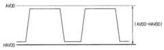
도 4는 본 발명의 일 실시예에 따른 충전률 열세 패턴을 설명하기 위한 파형도이다. 도 5는 본 발명의 일 실시예에 따른 오버 드라이빙 및 언더 드라이빙을 설명하기 위한 파형도이다.4 is a waveform diagram for explaining a charging rate inferior pattern according to an embodiment of the present invention. 5 is a waveform diagram for explaining overdriving and underdriving according to an embodiment of the present invention.
도 4를 참조하면, 상기 충전률 열세 패턴은 1 수평 주기 동안 충전 시간이 부족하여 화소에 충전되는 충전 데이터 전압이 화소에 인가되는 출력 데이터 전압에 못 미치는 경우이다. 예를 들면, 상기 충전률 열세 패턴은 시안, 마젠타, 옐로우 등과 같은 혼색 데이터와 같이 수평 주기 마다 데이터 전압의 변화가 큰 경우 심하게 발생할 수 있다.Referring to FIG. 4 , the charge rate inferior pattern is a case where the charging data voltage charged to the pixel is less than the output data voltage applied to the pixel due to insufficient charging time during one horizontal period. For example, the charge rate inferiority pattern may occur severely when a data voltage change per horizontal period is large, such as mixed color data such as cyan, magenta, and yellow.
제n-1 수평 라인(Hn-1)의 화소에는 224 계조 데이터에 대응하는 출력 데이터 전압, 약 14.2 V 를 출력하고, 제n 수평 라인(Hn)의 화소에는 0 계조 데이터에 대응하는 출력 데이터 전압, 약 8.0 V 를 출력한다.An output data voltage of about 14.2 V corresponding to 224 grayscale data is output to the pixel of the n-1th horizontal line Hn-1, and an output data voltage corresponding to 0 grayscale data to the pixel of the nth horizontal line Hn. , outputs about 8.0 V.
이 경우, 제n 수평 라인(Hn)의 화소는 충전 데이터 전압, 약 9.3 V 를 충전한다. 따라서, 상기 제n 수평 라인(Hn)의 화소는 출력 데이터 전압, 약 8.0V 에 못 미치는 충전 데이터 전압, 약 9.3 V 를 충전한다.In this case, the pixels of the nth horizontal line Hn are charged with the charging data voltage of about 9.3 V. Accordingly, the pixel of the nth horizontal line Hn is charged with a charge data voltage of about 9.3 V, which is less than the output data voltage of about 8.0 V.
이와 같이, 상기 제n 수평 라인(Hn)의 화소는 충전 시간 부족으로 출력 데이터 전압과 충전 데이터 전압 사이에 약 1 V 의 전압 차이를 발생하고 이로 인해 화질 불량이 발생할 수 있다.As such, the pixel of the nth horizontal line Hn generates a voltage difference of about 1 V between the output data voltage and the charged data voltage due to lack of charging time, which may cause image quality defects.
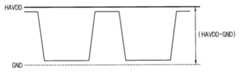
도 5를 참조하면, 제n-1 수평 라인(Hn-1)의 화소에는 224 계조 데이터에 대응하는 출력 데이터 전압, 약 14.2 V 를 출력하고, 제n 수평 라인의 화소에는 0 계조 데이터에 대응하는 출력 데이터 전압, 약 8.0 V 를 출력하고, 제n+1 수평 라인(Hn+1)의 화소에는 224 계조 데이터에 대응하는 출력 데이터 전압, 약14.2 V 를 출력한다.Referring to FIG. 5, an output data voltage of about 14.2 V corresponding to 224 grayscale data is output to the pixels of the n−1th horizontal line Hn−1, and an output data voltage corresponding to 0 grayscale data is output to the pixels of the nth horizontal line Hn−1. An output data voltage of about 8.0 V is output, and an output data voltage of about 14.2 V corresponding to 224 grayscale data is output to the pixels of the n+1th horizontal line (Hn+1).
본 실시예에 따르면, 상기 제n-1 수평 라인(Hn-1)의 화소는 제1 기준값인 200 계조 데이터 보다 큰224 계조 데이터를 갖고, 제n 수평 라인(Hn)의 화소는 제2 기준값인 0 계조 데이터와 같은 계조 데이터를 가지므로 상기 제n 수평 라인(Hn)의 화소는 충전률 열세 패턴의 조건을 만족할 수 있다.According to this embodiment, the pixels of the n−1 th horizontal line Hn−1 have 224 grayscale data greater than 200 grayscale data which is the first reference value, and the pixels of the nth horizontal line Hn have the second reference value Since it has the same grayscale data as the 0 grayscale data, the pixels of the nth horizontal line Hn may satisfy the condition of the thirteenth fill rate pattern.
따라서, 상기 데이터 구동부는 상기 제n 수평 라인(Hn)의 화소에 출력 데이터 전압으로 0 계조 영상 데이터의 데이터 전압인 8.0 V 보다 설정 전압인 2 V 만큼 낮은 언더 드라이빙 데이터 전압, 약 6.0 V 를 출력한다. 이에 따라서 상기 제n 수평 라인(Hn)의 화소는 0 계조 영상 데이터의 데이터 전압인 8.0 V에 도달하는 시간을 줄일 수 있다.Accordingly, the data driver outputs an under-driving data voltage of about 6.0 V, which is lower than the data voltage of 0 grayscale image data by 2 V, as an output data voltage to the pixel of the nth horizontal line Hn. . Accordingly, the time required for the pixels of the nth horizontal line Hn to reach 8.0 V, which is the data voltage of 0 grayscale image data, can be reduced.
한편, 제n 수평 라인(Hn)의 화소가 제2 기준값인 0 계조 데이터와 같은 계조 데이터이고, 상기 제n+1 수평 라인(Hn+1)의 화소가 제1 기준값인 200 계조 데이터보다 큰 224 계조 데이터인 경우, 상기 제n+1 수평 라인(Hn+1)의 화소는 충전률 열세 패턴의 조건을 만족할 수 있다.Meanwhile, pixels of the nth horizontal line Hn have the same grayscale data as the second reference value, 0 grayscale data, and pixels of the n+1th horizontal line Hn+1 are greater than 200 grayscale data, the first reference value 224 In the case of grayscale data, the pixels of the n+1th horizontal line (Hn+1) may satisfy the condition of the thirteenth fill factor pattern.
따라서, 상기 데이터 구동부는 상기 제n+1 수평 라인(Hn+1)의 화소에 출력 데이터 전압으로 224 계조 영상 데이터의 데이터 전압인 14.2 V 보다 설정 전압인 2 V 만큼 높은 오버 드라이빙 데이터 전압, 약 16.2 V 를 출력한다. 이에 따라서 상기 제n+1 수평 라인(Hn+1)의 화소는 224 계조 영상 데이터의 데이터 전압인 14.2 V에 도달하는 시간을 줄일 수 있다.Therefore, the data driver has an overdriving data voltage higher than the data voltage of 224 grayscale image data, 14.2 V, by 2 V, about 16.2 V, as an output data voltage to the pixels of the n+1th horizontal line (Hn+1). output V. Accordingly, the time required for the pixels of the n+1th horizontal line Hn+1 to reach 14.2 V, which is the data voltage of 224 grayscale image data, can be reduced.
도 6은 본 발명의 일 실시예에 따른 표시 장치의 구동 방법을 설명하기 위한 흐름도이다. 도 7a 내지 도 7c는 본 발명의 일 실시예에 따른 출력 버퍼부의 구동방법을 설명하기 위한 개념도들이다. 도8a 내지 도 8c는 본 발명의 일 실시예에 따른 출력 버퍼부의 구동방법을 설명하기 위한 개념도들이다.6 is a flowchart illustrating a method of driving a display device according to an exemplary embodiment of the present invention. 7A to 7C are conceptual diagrams for explaining a method of driving an output buffer unit according to an embodiment of the present invention. 8A to 8C are conceptual diagrams for explaining a method of driving an output buffer unit according to an embodiment of the present invention.
도 2, 도 3 및 도 6을 참조하면, 상기 영상 데이터 분석부(230)는 상기 현재 수평 라인의 영상 데이터(LDATA(n))와 이전 수평 라인의 영상 데이터(LDATA(n-1))를 비교 연산하여 현재 수평 라인의 영상 데이터(LDATA(n))가 충전률 열세 패턴의 조건을 만족하는지를 판단한다(단계 S110).Referring to FIGS. 2, 3 and 6, the
상기 영상 데이터 분석부(230)는 상기 현재 수평 라인의 영상 데이터(LDATA(n))가 상기 충전률 열세 패턴의 조건을 만족할 때(단계 S130), 상기 데이터 구동부(500)를 제어하기 위한 오버 드라이빙 신호(ODS) 또는 언더 드라이빙 신호(UDS)를 출력한다(단계 S140).The
상기 데이터 구동부(500)의 상기 출력 버퍼부(570)는 상기 타이밍 제어부의 제어에 따라서 구동 전압 발생부로부터 아날로그 전원 전압(AVDD), 양극성 하프 전원 전압(P_HAVDD) 및 음극성 하프 전원 전압(N_HAVDD)을 수신한다.The
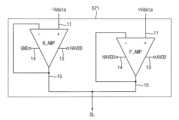
예를 들면, 도 7a를 참조하면, 상기 출력 버퍼부(570)는 k개 버퍼부들(571)을 포함한다. 각 버퍼부(571)는 양극성 데이터 전압을 증폭하여 출력하는 제1 증폭기(P_AMP) 및 음극성 데이터 전압을 증폭하여 출력하는 제2 증폭기(N_AMP)를 포함한다.For example, referring to FIG. 7A , the
상기 제1 및 제2 증폭기들(P_AMP, N_AMP) 각각은 입력 전압을 수신하는 입력 단자(11), 하이 전원 전압을 수신하는 제1 전원 단자(13), 로우 전원 전압을 수신하는 제2 전원 단자(14) 및 출력 전압을 출력하는 출력 단자(15)를 포함한다.Each of the first and second amplifiers P_AMP and N_AMP has an
상기 버퍼부(571)는 선택된 데이터 구동 전압으로서, 아날로그 전원 전압(AVDD), 양극성 하프 전원 전압(P_HAVDD) 및 음극성 하프 전원 전압(N_HAVDD)을 수신한다.The
예를 들면, 양극성 전압을 증폭하는 제1 증폭기(P_AMP)를 참조하면, 입력 단자(11)는 양극성 데이터 전압(+Vdata)을 수신하고, 제1 전원 단자는 하이 전원 전압인 아날로그 전원 전압(AVDD)을 수신하고, 제2 전원 단자는 로우 전원 전압인 양극성 하프 전원 전압(P_HAVDD)을 수신한다.For example, referring to the first amplifier (P_AMP) that amplifies the positive voltage, the
음극성 전압을 증폭하는 제2 증폭기(N_AMP)를 참조하면, 입력 단자(11)는 음극성 데이터 전압(-Vdata)을 수신하고, 제1 전원 단자(13)는 하이 전원 전압인 음극성 하프 전원 전압(N_HAVDD)을 수신하고, 제2 전원 단자(14)는 로우 전원 전압인 접지 전압(GND)을 수신한다.Referring to the second amplifier N_AMP that amplifies the negative voltage, the
상기 아날로그 전원 전압(AVDD), 양극성 하프 전원 전압(P_HAVDD) 및 음극성 하프 전원 전압(N_HAVDD)의 전압 레벨은 AVDD > N_HAVDD > P_HAVDD > GND 와 같다.The voltage levels of the analog power supply voltage AVDD, the positive half power supply voltage P_HAVDD, and the negative half power supply voltage N_HAVDD are equal to AVDD > N_HAVDD > P_HAVDD > GND.
도 7b를 참조하면, 상기 제1 증폭기(P_AMP)를 통해서 양극성 오버 드라이빙 데이터 전압 및 언더 드라이빙 데이터 전압은 아날로그 전원 전압(AVDD)과 상기 양극성 하프 전원 전압(P_HAVDD) 사이의 전압 범위에서 증폭되어 출력될 수 있다.Referring to FIG. 7B, the positive overdriving data voltage and the underdriving data voltage are amplified and output in a voltage range between the analog power supply voltage AVDD and the positive half power supply voltage P_HAVDD through the first amplifier P_AMP. can
도 7c를 참조하면, 상기 제2 증폭기(N_AMP)를 통해서 음극성 오버 드라이빙 데이터 전압 및 언더 드라이빙 데이터 전압은 상기 음극성 하프 전원 전압(N_HAVDD)과 접지 전압(GND) 사이의 전압 범위에서 증폭되어 출력될 수 있다.Referring to FIG. 7C , the negative overdriving data voltage and the underdriving data voltage are amplified in a voltage range between the negative half power supply voltage N_HAVDD and the ground voltage GND through the second amplifier N_AMP, and are then output. It can be.
상기 출력 버퍼부(570)에서 증폭된 수평 라인의 오버 드라이빙 또는 언더 드라이빙 데이터 전압은 데이터 라인에 제공된다.The overdriving or underdriving data voltage of the horizontal line amplified by the
한편, 상기 영상 데이터 분석부(230)는 상기 현재 수평 라인의 영상 데이터(LDATA(n))가 상기 충전률 열세 패턴의 조건을 만족하지 않으면(단계 S130), 상기 데이터 구동부(500)를 제어하기 위한 오버 드라이빙 신호(ODS) 또는 언더 드라이빙 신호(UDS)를 출력하지 않는다.Meanwhile, the
따라서, 상기 데이터 구동부(500)의 상기 출력 버퍼부(570)는 상기 타이밍 제어부의 제어에 따라서 구동 전압 발생부로부터 아날로그 전원 전압(AVDD) 및 하프 전원 전압(HAVDD)을 수신한다.Accordingly, the
예를 들면, 도 8a를 참조하면, 상기 버퍼부(571)는 아날로그 전원 전압(AVDD) 및 하프 전원 전압(HAVDD)을 수신한다(단계 S170).For example, referring to FIG. 8A , the
예를 들면, 양극성 전압을 증폭하는 제1 증폭기(P_AMP)를 참조하면, 입력 단자(11)는 양극성 데이터 전압(+Vdata)을 수신하고, 제1 전원 단자(13)는 하이 전원 전압인 아날로그 전원 전압(AVDD)을 수신하고, 제2 전원 단자(14)는 로우 전원 전압인 하프 전원 전압(HAVDD)을 수신한다.For example, referring to the first amplifier (P_AMP) that amplifies the positive voltage, the
음극성 전압을 증폭하는 제2 증폭기(N_AMP)를 참조하면, 입력 단자(11)는 음극성 데이터 전압(-Vdata)을 수신하고, 제1 전원 단자(13)는 하이 전원 전압인 상기 하프 전원 전압(HAVDD)을 수신하고, 제2 전원 단자(14)는 로우 전원 전압인 접지 전압(GND)을 수신한다.Referring to the second amplifier N_AMP that amplifies the negative voltage, the
상기 하프 전원 전압(HAVDD)의 전압 레벨은 도 5a를 참조하면, N_HAVDD > HAVDD > P_HAVDD 와 같다.Referring to FIG. 5A , the voltage level of the half power supply voltage HAVDD is equal to N_HAVDD > HAVDD > P_HAVDD.
도 8b를 참조하면, 상기 제1 증폭기(P_AMP)를 통해서 양극성 데이터 전압은 아날로그 전원 전압(AVDD)과 상기 하프 전원 전압(HAVDD) 사이의 전압 범위에서 증폭되어 출력될 수 있다.Referring to FIG. 8B , the positive data voltage may be amplified and output in a voltage range between the analog power supply voltage AVDD and the half power supply voltage HAVDD through the first amplifier P_AMP.
도 8c를 참조하면, 상기 제2 증폭기(N_AMP)를 통해서 음극성 데이터전압은 상기 하프 전원 전압(HAVDD)과 접지 전압(GND) 사이의 전압 범위에서 증폭되어 출력될 수 있다.Referring to FIG. 8C , the negative data voltage may be amplified and output in a voltage range between the half power supply voltage HAVDD and the ground voltage GND through the second amplifier N_AMP.
상기 출력 버퍼부(570)에서 증폭된 수평 라인의 데이터 전압은 데이터 라인에 제공된다.The data voltage of the horizontal line amplified by the
도 9는 비교예 및 실시예에 따른 출력 버퍼부의 출력 전압 범위에 대한 충전 데이터 전압을 설명하기 위한 파형도이다.9 is a waveform diagram for explaining a charging data voltage with respect to an output voltage range of an output buffer unit according to comparative examples and embodiments.
도 9를 참조하면, 제n-1 수평 라인(Hn-1)의 영상 데이터가 제1 기준값인 200 계조 보다 큰 224 계조를 갖고, 제n 수평 라인(Hn)의 영상 데이터가 제2 기준값인 0 계조와 같은 0 계조를 가지므로 상기 제n 수평 라인의 영상 데이터는 충전률 열세 패턴의 조건을 만족할 수 있다.Referring to FIG. 9 , the image data of the n−1 th horizontal line Hn−1 has 224 gray levels greater than the first reference value of 200 gray levels, and the image data of the n th horizontal line Hn has a second reference value of 0 Since it has the same gradation as 0, the image data of the nth horizontal line can satisfy the condition of the thirteenth fill rate pattern.
따라서, 상기 데이터 구동부는 상기 제n 수평 라인(Hn)의 화소에 출력 데이터 전압으로 0 계조 영상 데이터의 8.0 V 보다 설정 전압인 1.2 V 만큼 낮은 언더 드라이빙 데이터 전압, 약 6.8 V 를 출력한다.Accordingly, the data driver outputs an under-driving data voltage of about 6.8 V, which is lower than 8.0 V of grayscale image data by 1.2 V, as an output data voltage to the pixel on the n-th horizontal line Hn.
비교예에 따르면, 출력 버퍼부는 양극성의 언더 드라이빙 데이터 전압, 6.8 V를 아날로그 전원 전압(AVDD)인 약15 V와 하프 전원 전압(HAVDD)인 약7.5 V 사이의 전압 범위에서 증폭하여 출력한다.According to the comparative example, the output buffer unit amplifies and outputs the positive under-driving data voltage, 6.8 V, in a voltage range between about 15 V, which is an analog power supply voltage (AVDD), and about 7.5 V, which is a half power supply voltage (HAVDD).
따라서, 상기 언더 드라이빙 데이터 전압, 약 6.8 V 는 상기 출력 버퍼부의 출력 전압 범위를 벗어나게 되어 언더 드라이빙 적용 범위의 제한을 받게 된다.Accordingly, the under-driving data voltage of about 6.8 V is out of the output voltage range of the output buffer unit, and thus the under-driving application range is limited.
비교예의 출력 버퍼부에 의하면, 제n 수평 라인의 화소에는 약 9.3 V의 충전 데이터 전압이 충전된다.According to the output buffer unit of the comparative example, a charge data voltage of about 9.3 V is charged to the pixels of the nth horizontal line.
한편, 실시예에 따르면, 출력 버퍼부는 양극성의 언더 드라이빙 데이터 전압, 6.8 V를 아날로그 전원 전압(AVDD)인 약 15 V와 양극성 하프 전원 전압(P_HAVDD)인 약 6 V 사이의 전압 범위에서 증폭하여 출력한다.Meanwhile, according to the embodiment, the output buffer unit amplifies the positive under-driving data voltage, 6.8 V, in a voltage range between about 15 V, which is an analog power supply voltage (AVDD), and about 6 V, which is a positive half power supply voltage (P_HAVDD), and outputs the amplified voltage. do.
따라서, 상기 언더 드라이빙 데이터 전압, 약 6.8 V 는 상기 출력 버퍼부의 출력 전압 범위 내에 포함되므로 언더 드라이빙 적용 범위의 제한을 막을 수 있다.Accordingly, since the under-driving data voltage of about 6.8 V is included within the output voltage range of the output buffer unit, the limitation of the under-driving application range may be prevented.
실시예의 출력 버퍼부에 의하면, 제n 수평 라인의 화소에는 약 8.0 V의 충전 데이터 전압이 충전되므로 충전률 개선을 위한 언더 드라이빙을 수행할 수 있다.According to the output buffer unit of the embodiment, since the charging data voltage of about 8.0 V is charged to the pixels of the n-th horizontal line, under-driving for improving the charging rate may be performed.
이상의 실시예들에 따르면, 수평 라인의 영상 데이터가 충전률 열세 패턴 조건을 만족할 때, 수평 라인의 데이터 전압을 오버 드라이빙 또는 언더 드라이빙 데이터 전압으로 보상하고, 출력 버퍼부의 전원 전압 범위를 오버 드라이빙 또는 언더 드라이빙 데이터 전압을 포함하도록 조절하여 상기 오버 드라이빙 데이터 전압 또는 언더 드라이빙 데이터 전압을 버퍼링하여 출력한다. 이에 따라서 충전률 저하에 따른 화질 불량을 개선할 수 있다.According to the above embodiments, when the image data of the horizontal line satisfies the charging rate inferiority pattern condition, the data voltage of the horizontal line is compensated with an over-driving or under-driving data voltage, and the power supply voltage range of the output buffer unit is over-driving or under-driving. The driving data voltage is adjusted to include the driving data voltage, and the overdriving data voltage or the underdriving data voltage is buffered and output. Accordingly, it is possible to improve image quality defects due to a decrease in the charging rate.
또한, 수평 라인의 영상 데이터가 충전률 열세 패턴이 아닌 경우, 출력 버퍼부의 전원 전압 범위를 정상적 범위로 조절함으로써 소비 전력 및 발열을 최소화할 수 있다.In addition, when the image data of the horizontal line does not have an inferior charging rate pattern, power consumption and heat generation can be minimized by adjusting the power supply voltage range of the output buffer unit to a normal range.
본 발명은 표시 장치 및 이를 포함하는 다양한 장치 및 시스템에 적용될 수 있다. 따라서 본 발명은 휴대폰, 스마트 폰, PDA, PMP, 디지털 카메라, 캠코더, PC, 서버 컴퓨터, 워크스테이션, 노트북, 디지털 TV, 셋-탑 박스, 음악 재생기, 휴대용 게임 콘솔, 네비게이션 시스템, 스마트 카드, 프린터 등과 같은 다양한 전자 기기에 유용하게 이용될 수 있다.The present invention can be applied to a display device and various devices and systems including the display device. Accordingly, the present invention relates to mobile phones, smart phones, PDAs, PMPs, digital cameras, camcorders, PCs, server computers, workstations, notebooks, digital TVs, set-top boxes, music players, portable game consoles, navigation systems, smart cards, and printers. It can be usefully used in various electronic devices such as
상기에서는 본 발명의 바람직한 실시예를 참조하여 설명하였지만, 해당 기술분야의 숙련된 당업자는 하기의 특허청구범위에 기재된 본 발명의 사상 및 영역으로부터 벗어나지 않는 범위 내에서 본 발명을 다양하게 수정 및 변경시킬 수 있음을 이해할 것이다.Although the above has been described with reference to preferred embodiments of the present invention, those skilled in the art can variously modify and change the present invention without departing from the spirit and scope of the present invention described in the claims below. you will understand that you can
Claims (20)
Translated fromKorean이전 수평 라인의 영상 데이터와 현재 수평 라인의 영상 데이터를 분석하여 상기 현재 수평 라인의 영상 데이터가 충전률 열세 패턴의 조건을 만족하는지는 판단하는 영상 데이터 분석부; 및
상기 현재 수평 라인의 영상 데이터가 충전률 열세 패턴의 조건을 만족할 때, 양극성 데이터 전압을 증폭하여 상기 데이터 라인에 출력하는 제1 증폭기의 로우 전원 단자와 음극성 데이터 전압을 증폭하여 상기 데이터 라인에 출력하는 제2 증폭기의 하이 전원 단자는 서로 다른 레벨의 전원 전압을 수신하는 출력 버퍼부를 포함하는 표시 장치.a display panel including a data line and sub-pixels of different colors, wherein the sub-pixels of different colors are connected to the same data line;
an image data analysis unit that analyzes image data of a previous horizontal line and image data of a current horizontal line to determine whether the image data of the current horizontal line satisfies a condition of a filling rate inferior pattern; and
When the image data of the current horizontal line satisfies the condition of the thirteenth charging rate pattern, the low power terminal of the first amplifier that amplifies the positive data voltage and outputs it to the data line and amplifies the negative data voltage and outputs it to the data line and an output buffer receiving power supply voltages of different levels from the high power supply terminals of the second amplifier.
상기 제2 증폭기의 하이 전원 단자는 상기 하프 전원 전압 보다 높은 레벨의 음극성 하프 전원 전압을 수신하는 것을 특징으로 하는 표시 장치.3. The method of claim 2, wherein the low power supply terminal of the first amplifier receives a positive half power supply voltage having a lower level than a half power supply voltage that is a half level of the analog power supply voltage;
The display device of claim 1 , wherein the high power supply terminal of the second amplifier receives a negative half power supply voltage having a higher level than the half power supply voltage.
상기 이전 수평 라인의 영상 데이터가 상기 제2 기준값보다 작거나 같고, 상기 현재 수평 라인의 영상 데이터가 상기 제1 기준값보다 크거나 같은 조건을 만족할 때, 상기 현재 수평 라인의 영상 데이터는 오버 드라이빙 데이터 전압으로 보상하는 것을 특징으로 하는 표시 장치.The method of claim 5 , wherein when the image data of the previous horizontal line is greater than or equal to a first reference value and the image data of the current horizontal line is less than or equal to a second reference value, the image data of the current horizontal line is Compensate with under-driving data voltage,
When the video data of the previous horizontal line is less than or equal to the second reference value and the video data of the current horizontal line is greater than or equal to the first reference value, the video data of the current horizontal line is an overdriving data voltage A display device characterized in that for compensation.
상기 제1 증폭기의 하이 전원 단자는 상기 아날로그 전원 전압을 수신하고, 상기 제2 증폭기의 로우 전원 단자는 접지 전압을 수신하는 것을 특징으로 하는 표시 장치.9. The method of claim 8, wherein the low power terminal of the first amplifier and the high power terminal of the second amplifier receive a half power supply voltage that is a half level of the analog power supply voltage;
The high power terminal of the first amplifier receives the analog power voltage, and the low power terminal of the second amplifier receives a ground voltage.
상기 데이터 전압은 상기 제1 증폭기 또는 제2증폭기의 입력 단자에 입력되는 것을 특징으로 하는 표시 장치.10. The method of claim 9, further comprising a digital-to-analog converter converting the image data of the current horizontal line into a data voltage using a gamma voltage,
The display device according to claim 1 , wherein the data voltage is input to an input terminal of the first amplifier or the second amplifier.
이전 수평 라인의 영상 데이터와 현재 수평 라인의 영상 데이터를 분석하여 상기 현재 수평 라인의 영상 데이터가 충전률 열세 패턴의 조건을 만족하는지는 판단하는 단계; 및
상기 현재 수평 라인의 영상 데이터가 충전률 열세 패턴의 조건을 만족할 때, 양극성 데이터 전압을 증폭하여 상기 데이터 라인에 출력하는 제1 증폭기의 로우 전원 단자와 음극성 데이터 전압을 증폭하여 상기 데이터 라인에 출력하는 제2 증폭기의 하이 전원 단자는 서로 다른 레벨의 전원 전압을 수신하는 단계를 포함하는 표시 장치의 구동 방법.In a method of driving a display device including a data line and sub-pixels of different colors, wherein the sub-pixels of different colors are connected to the same data line,
analyzing image data of a previous horizontal line and image data of a current horizontal line to determine whether the image data of the current horizontal line satisfies a condition of a filling rate inferior pattern; and
When the image data of the current horizontal line satisfies the condition of the thirteenth charging rate pattern, the low power supply terminal of the first amplifier that amplifies the positive data voltage and outputs it to the data line and amplifies the negative data voltage and outputs it to the data line and receiving power supply voltages of different levels from a high power supply terminal of a second amplifier.
상기 제2 증폭기의 하이 전원 단자는 상기 하프 전원 전압 보다 높은 레벨의 음극성 하프 전원 전압을 수신하는 것을 특징으로 하는 표시 장치의 구동 방법.13. The method of claim 12, wherein the low power supply terminal of the first amplifier receives a positive half power supply voltage at a level lower than a half power supply voltage that is a half level of the analog power supply voltage;
and a high power supply terminal of the second amplifier receives a negative half power supply voltage having a higher level than the half power supply voltage.
상기 이전 수평 라인의 영상 데이터가 상기 제2 기준값보다 작거나 같고, 상기 현재 수평 라인의 영상 데이터가 상기 제1 기준값보다 크거나 같은 조건을 만족할 때, 상기 현재 수평 라인의 영상 데이터는 오버 드라이빙 데이터 전압으로 보상하는 것을 특징으로 하는 표시 장치의 구동 방법.16. The method of claim 15, wherein when the image data of the previous horizontal line is greater than or equal to a first reference value and the image data of the current horizontal line is less than or equal to a second reference value, the image data of the current horizontal line is Compensate with under-driving data voltage,
When the video data of the previous horizontal line is less than or equal to the second reference value and the video data of the current horizontal line is greater than or equal to the first reference value, the video data of the current horizontal line is an overdriving data voltage A driving method of a display device, characterized in that for compensating with
상기 제1 증폭기의 하이 전원 단자는 상기 아날로그 전원 전압이고, 상기 제2 증폭기의 로우 전원 단자는 접지 전압을 수신하는 것을 특징으로 하는 표시 장치의 구동 방법.19. The method of claim 18, wherein the low power terminal of the first amplifier and the high power terminal of the second amplifier receive a half power supply voltage that is a half level of the analog power supply voltage;
and a high power terminal of the first amplifier receives the analog power voltage, and a low power terminal of the second amplifier receives a ground voltage.
상기 데이터 전압은 상기 제1 증폭기 또는 제2 증폭기의 입력 단자에 입력되는 것을 특징으로 하는 표시 장치의 구동 방법.20. The method of claim 19, further comprising converting the image data of the current horizontal line into a data voltage using a gamma voltage,
The method of driving a display device, wherein the data voltage is input to an input terminal of the first amplifier or the second amplifier.
Priority Applications (3)
| Application Number | Priority Date | Filing Date | Title |
|---|---|---|---|
| KR1020180067135AKR102525974B1 (en) | 2018-06-12 | 2018-06-12 | Display device and method of driving the same |
| US16/380,388US10847110B2 (en) | 2018-06-12 | 2019-04-10 | Display device and method of driving the same |
| CN201910501320.8ACN110599970B (en) | 2018-06-12 | 2019-06-11 | Display device and method of driving the same |
Applications Claiming Priority (1)
| Application Number | Priority Date | Filing Date | Title |
|---|---|---|---|
| KR1020180067135AKR102525974B1 (en) | 2018-06-12 | 2018-06-12 | Display device and method of driving the same |
Publications (2)
| Publication Number | Publication Date |
|---|---|
| KR20190141039A KR20190141039A (en) | 2019-12-23 |
| KR102525974B1true KR102525974B1 (en) | 2023-04-27 |
Family
ID=68763595
Family Applications (1)
| Application Number | Title | Priority Date | Filing Date |
|---|---|---|---|
| KR1020180067135AActiveKR102525974B1 (en) | 2018-06-12 | 2018-06-12 | Display device and method of driving the same |
Country Status (3)
| Country | Link |
|---|---|
| US (1) | US10847110B2 (en) |
| KR (1) | KR102525974B1 (en) |
| CN (1) | CN110599970B (en) |
Families Citing this family (6)
| Publication number | Priority date | Publication date | Assignee | Title |
|---|---|---|---|---|
| KR102673056B1 (en) | 2020-03-10 | 2024-06-10 | 주식회사 엘엑스세미콘 | Data processing device for compensating data and display device |
| KR102650708B1 (en)* | 2020-03-20 | 2024-03-25 | 삼성디스플레이 주식회사 | Display apparatus and method of driving the same |
| KR102714382B1 (en)* | 2020-04-02 | 2024-10-10 | 주식회사 엘엑스세미콘 | Device and Method for Driving Display |
| KR102862795B1 (en)* | 2020-12-31 | 2025-09-22 | 엘지디스플레이 주식회사 | Display Device and Driving Method of the same |
| KR102809085B1 (en)* | 2021-04-13 | 2025-05-20 | 삼성디스플레이 주식회사 | Display apparatus and method of driving display panel using the same |
| CN117795591A (en) | 2022-06-17 | 2024-03-29 | 京东方科技集团股份有限公司 | Driving method, driving circuit, driving chip and display device of display panel |
Family Cites Families (18)
| Publication number | Priority date | Publication date | Assignee | Title |
|---|---|---|---|---|
| KR100590747B1 (en) | 1999-01-30 | 2006-06-15 | 삼성전자주식회사 | Liquid crystal display fine-tuning the difference between different common voltages |
| KR20070067968A (en) | 2005-12-26 | 2007-06-29 | 삼성전자주식회사 | Gamma voltage generation method and apparatus, liquid crystal display using same and driving method thereof |
| CN101467200B (en)* | 2006-09-28 | 2011-09-28 | 夏普株式会社 | Liquid crystal display device, driving circuit and driving method thereof |
| JP4501084B2 (en)* | 2006-10-10 | 2010-07-14 | エプソンイメージングデバイス株式会社 | Liquid crystal display device and power supply circuit |
| JP5770266B2 (en)* | 2011-04-08 | 2015-08-26 | シャープ株式会社 | Display device |
| KR20150033156A (en)* | 2013-09-23 | 2015-04-01 | 삼성디스플레이 주식회사 | Display device and driving method thereof |
| KR102138369B1 (en)* | 2013-10-10 | 2020-07-28 | 삼성전자주식회사 | Display drive circuit, display device and portable terminal comprising thereof |
| KR20150076442A (en) | 2013-12-26 | 2015-07-07 | 엘지디스플레이 주식회사 | Liquid crystal display |
| KR102278743B1 (en)* | 2014-03-14 | 2021-07-19 | 엘지디스플레이 주식회사 | Liquid Crystal Display and Driving Method thereof |
| KR102342739B1 (en)* | 2014-10-13 | 2021-12-24 | 삼성디스플레이 주식회사 | Method of driving display panel and display apparatus for performing the method |
| KR20160082402A (en)* | 2014-12-26 | 2016-07-08 | 삼성디스플레이 주식회사 | Display apparatus and method of driving display panel using the same |
| TWI688211B (en) | 2015-01-29 | 2020-03-11 | 日商半導體能源研究所股份有限公司 | Semiconductor device, electronic component, and electronic device |
| CN104766564B (en)* | 2015-04-24 | 2017-03-15 | 京东方科技集团股份有限公司 | A kind of display floater, its driving method and display device |
| KR102501906B1 (en)* | 2016-03-08 | 2023-02-22 | 엘지디스플레이 주식회사 | Liquid crystal display device and driving method thereof |
| CN105702226B (en)* | 2016-04-28 | 2018-07-17 | 京东方科技集团股份有限公司 | A kind of driving method of display panel, display panel and display device |
| CN105913825A (en)* | 2016-06-30 | 2016-08-31 | 京东方科技集团股份有限公司 | Liquid crystal display driving method, liquid crystal display and display device |
| KR102566655B1 (en) | 2016-07-11 | 2023-08-14 | 삼성디스플레이 주식회사 | Display device |
| CN106409252A (en)* | 2016-09-22 | 2017-02-15 | 京东方科技集团股份有限公司 | Array substrate and driving method thereof, display panel and display device |
- 2018
- 2018-06-12KRKR1020180067135Apatent/KR102525974B1/enactiveActive
- 2019
- 2019-04-10USUS16/380,388patent/US10847110B2/enactiveActive
- 2019-06-11CNCN201910501320.8Apatent/CN110599970B/enactiveActive
Also Published As
| Publication number | Publication date |
|---|---|
| KR20190141039A (en) | 2019-12-23 |
| CN110599970B (en) | 2022-11-08 |
| CN110599970A (en) | 2019-12-20 |
| US10847110B2 (en) | 2020-11-24 |
| US20190378471A1 (en) | 2019-12-12 |
Similar Documents
| Publication | Publication Date | Title |
|---|---|---|
| KR102525974B1 (en) | Display device and method of driving the same | |
| KR101692856B1 (en) | Method of driving display panel and display apparatus for performing the method | |
| CN111179798A (en) | Display device and driving method thereof | |
| KR101639308B1 (en) | Method of driving display panel and display apparatus for performing the method | |
| KR101798489B1 (en) | Device for generating gamma, LCD and Method for driving the LCD | |
| KR101232161B1 (en) | Apparatus and method for driving liquid crystal display device | |
| KR102050850B1 (en) | Method of driving display panel and display apparatus for performing the same | |
| KR101521656B1 (en) | Liquid crystal display | |
| KR20080107064A (en) | LCD and its driving method | |
| KR20110067355A (en) | Driving device for video display device and its driving method | |
| CN110827772B (en) | Display device and method of driving the same | |
| KR100864497B1 (en) | Liquid crystal display | |
| KR20150094872A (en) | Display device and driving method thereof | |
| KR101278001B1 (en) | Driving liquid crystal display and apparatus for driving the same | |
| KR20120098139A (en) | Method of driving display panel and display apparatus for performing the same | |
| KR20110039006A (en) | Large screen liquid crystal display | |
| KR101323469B1 (en) | Driving liquid crystal display and apparatus for driving the same | |
| KR20110078375A (en) | Liquid crystal display device and driving method thereof | |
| KR20170105176A (en) | Liquid crystal display device and driving method thereof | |
| KR101777126B1 (en) | Driving apparatus for liquid crystal display device and method for driving the same | |
| US20140078188A1 (en) | Driving device of display device | |
| KR102270603B1 (en) | Liquid Crystal Display | |
| KR102298315B1 (en) | Display Device | |
| KR102066135B1 (en) | Liquid crystal display device and driving method thereof | |
| KR101415686B1 (en) | Source driving circuit and driving method thereof |
Legal Events
| Date | Code | Title | Description |
|---|---|---|---|
| PA0109 | Patent application | St.27 status event code:A-0-1-A10-A12-nap-PA0109 | |
| R18-X000 | Changes to party contact information recorded | St.27 status event code:A-3-3-R10-R18-oth-X000 | |
| PG1501 | Laying open of application | St.27 status event code:A-1-1-Q10-Q12-nap-PG1501 | |
| A201 | Request for examination | ||
| PA0201 | Request for examination | St.27 status event code:A-1-2-D10-D11-exm-PA0201 | |
| E902 | Notification of reason for refusal | ||
| PE0902 | Notice of grounds for rejection | St.27 status event code:A-1-2-D10-D21-exm-PE0902 | |
| P11-X000 | Amendment of application requested | St.27 status event code:A-2-2-P10-P11-nap-X000 | |
| P13-X000 | Application amended | St.27 status event code:A-2-2-P10-P13-nap-X000 | |
| E701 | Decision to grant or registration of patent right | ||
| PE0701 | Decision of registration | St.27 status event code:A-1-2-D10-D22-exm-PE0701 | |
| PR0701 | Registration of establishment | St.27 status event code:A-2-4-F10-F11-exm-PR0701 | |
| PR1002 | Payment of registration fee | St.27 status event code:A-2-2-U10-U11-oth-PR1002 Fee payment year number:1 | |
| PG1601 | Publication of registration | St.27 status event code:A-4-4-Q10-Q13-nap-PG1601 |