KR102521372B1 - Method for predicting location of a mark - Google Patents
Method for predicting location of a markDownload PDFInfo
- Publication number
- KR102521372B1 KR102521372B1KR1020160016475AKR20160016475AKR102521372B1KR 102521372 B1KR102521372 B1KR 102521372B1KR 1020160016475 AKR1020160016475 AKR 1020160016475AKR 20160016475 AKR20160016475 AKR 20160016475AKR 102521372 B1KR102521372 B1KR 102521372B1
- Authority
- KR
- South Korea
- Prior art keywords
- image information
- mark
- sawing
- unit
- substrate
- Prior art date
- Legal status (The legal status is an assumption and is not a legal conclusion. Google has not performed a legal analysis and makes no representation as to the accuracy of the status listed.)
- Active
Links
Images


Classifications
- H—ELECTRICITY
- H01—ELECTRIC ELEMENTS
- H01L—SEMICONDUCTOR DEVICES NOT COVERED BY CLASS H10
- H01L23/00—Details of semiconductor or other solid state devices
- H01L23/544—Marks applied to semiconductor devices or parts, e.g. registration marks, alignment structures, wafer maps
- G—PHYSICS
- G06—COMPUTING OR CALCULATING; COUNTING
- G06T—IMAGE DATA PROCESSING OR GENERATION, IN GENERAL
- G06T7/00—Image analysis
- G06T7/70—Determining position or orientation of objects or cameras
- G06T7/73—Determining position or orientation of objects or cameras using feature-based methods
- G—PHYSICS
- G06—COMPUTING OR CALCULATING; COUNTING
- G06T—IMAGE DATA PROCESSING OR GENERATION, IN GENERAL
- G06T7/00—Image analysis
- G06T7/0002—Inspection of images, e.g. flaw detection
- G06T7/0004—Industrial image inspection
- G—PHYSICS
- G06—COMPUTING OR CALCULATING; COUNTING
- G06T—IMAGE DATA PROCESSING OR GENERATION, IN GENERAL
- G06T7/00—Image analysis
- G06T7/0002—Inspection of images, e.g. flaw detection
- G06T7/0004—Industrial image inspection
- G06T7/0006—Industrial image inspection using a design-rule based approach
- G—PHYSICS
- G06—COMPUTING OR CALCULATING; COUNTING
- G06T—IMAGE DATA PROCESSING OR GENERATION, IN GENERAL
- G06T7/00—Image analysis
- G06T7/70—Determining position or orientation of objects or cameras
- H—ELECTRICITY
- H01—ELECTRIC ELEMENTS
- H01L—SEMICONDUCTOR DEVICES NOT COVERED BY CLASS H10
- H01L21/00—Processes or apparatus adapted for the manufacture or treatment of semiconductor or solid state devices or of parts thereof
- H01L21/67—Apparatus specially adapted for handling semiconductor or electric solid state devices during manufacture or treatment thereof; Apparatus specially adapted for handling wafers during manufacture or treatment of semiconductor or electric solid state devices or components ; Apparatus not specifically provided for elsewhere
- H01L21/67005—Apparatus not specifically provided for elsewhere
- H01L21/67242—Apparatus for monitoring, sorting or marking
- H—ELECTRICITY
- H01—ELECTRIC ELEMENTS
- H01L—SEMICONDUCTOR DEVICES NOT COVERED BY CLASS H10
- H01L21/00—Processes or apparatus adapted for the manufacture or treatment of semiconductor or solid state devices or of parts thereof
- H01L21/70—Manufacture or treatment of devices consisting of a plurality of solid state components formed in or on a common substrate or of parts thereof; Manufacture of integrated circuit devices or of parts thereof
- H01L21/71—Manufacture of specific parts of devices defined in group H01L21/70
- H01L21/76—Making of isolation regions between components
- H—ELECTRICITY
- H01—ELECTRIC ELEMENTS
- H01L—SEMICONDUCTOR DEVICES NOT COVERED BY CLASS H10
- H01L21/00—Processes or apparatus adapted for the manufacture or treatment of semiconductor or solid state devices or of parts thereof
- H01L21/70—Manufacture or treatment of devices consisting of a plurality of solid state components formed in or on a common substrate or of parts thereof; Manufacture of integrated circuit devices or of parts thereof
- H01L21/77—Manufacture or treatment of devices consisting of a plurality of solid state components or integrated circuits formed in, or on, a common substrate
- H01L21/78—Manufacture or treatment of devices consisting of a plurality of solid state components or integrated circuits formed in, or on, a common substrate with subsequent division of the substrate into plural individual devices
- H—ELECTRICITY
- H01—ELECTRIC ELEMENTS
- H01L—SEMICONDUCTOR DEVICES NOT COVERED BY CLASS H10
- H01L22/00—Testing or measuring during manufacture or treatment; Reliability measurements, i.e. testing of parts without further processing to modify the parts as such; Structural arrangements therefor
- H01L22/10—Measuring as part of the manufacturing process
- H01L22/12—Measuring as part of the manufacturing process for structural parameters, e.g. thickness, line width, refractive index, temperature, warp, bond strength, defects, optical inspection, electrical measurement of structural dimensions, metallurgic measurement of diffusions
- H—ELECTRICITY
- H01—ELECTRIC ELEMENTS
- H01L—SEMICONDUCTOR DEVICES NOT COVERED BY CLASS H10
- H01L22/00—Testing or measuring during manufacture or treatment; Reliability measurements, i.e. testing of parts without further processing to modify the parts as such; Structural arrangements therefor
- H01L22/20—Sequence of activities consisting of a plurality of measurements, corrections, marking or sorting steps
- H01L22/26—Acting in response to an ongoing measurement without interruption of processing, e.g. endpoint detection, in-situ thickness measurement
- G—PHYSICS
- G06—COMPUTING OR CALCULATING; COUNTING
- G06T—IMAGE DATA PROCESSING OR GENERATION, IN GENERAL
- G06T2207/00—Indexing scheme for image analysis or image enhancement
- G06T2207/10—Image acquisition modality
- G06T2207/10016—Video; Image sequence
- G—PHYSICS
- G06—COMPUTING OR CALCULATING; COUNTING
- G06T—IMAGE DATA PROCESSING OR GENERATION, IN GENERAL
- G06T2207/00—Indexing scheme for image analysis or image enhancement
- G06T2207/30—Subject of image; Context of image processing
- G06T2207/30108—Industrial image inspection
- G06T2207/30148—Semiconductor; IC; Wafer
- G—PHYSICS
- G06—COMPUTING OR CALCULATING; COUNTING
- G06V—IMAGE OR VIDEO RECOGNITION OR UNDERSTANDING
- G06V10/00—Arrangements for image or video recognition or understanding
- G06V10/20—Image preprocessing
- G06V10/24—Aligning, centring, orientation detection or correction of the image
- G06V10/245—Aligning, centring, orientation detection or correction of the image by locating a pattern; Special marks for positioning
- G—PHYSICS
- G06—COMPUTING OR CALCULATING; COUNTING
- G06V—IMAGE OR VIDEO RECOGNITION OR UNDERSTANDING
- G06V2201/00—Indexing scheme relating to image or video recognition or understanding
- G06V2201/06—Recognition of objects for industrial automation
Landscapes
- Engineering & Computer Science (AREA)
- Physics & Mathematics (AREA)
- General Physics & Mathematics (AREA)
- Computer Vision & Pattern Recognition (AREA)
- Theoretical Computer Science (AREA)
- Manufacturing & Machinery (AREA)
- Computer Hardware Design (AREA)
- Microelectronics & Electronic Packaging (AREA)
- Power Engineering (AREA)
- Quality & Reliability (AREA)
- Condensed Matter Physics & Semiconductors (AREA)
- Container, Conveyance, Adherence, Positioning, Of Wafer (AREA)
- Length Measuring Devices By Optical Means (AREA)
Abstract
Translated fromKorean
Description
Translated fromKorean본 발명은 마크 위치 예측 방법에 관한 것이다.The present invention relates to a method for predicting a mark position.
반도체 패키지 공정은 기판에 포함된 복수의 전자 소자 영역들의 각각에 마크 및 소잉 표식을 표시하는 마킹 공정, 소잉 표식을 이용하여 전자 소자 영역들을 절단하는 소잉 공정 및 개별화된 전자 소자 영역들의 각각을 검사하는 검사 공정 을 포함할 수 있다. 반도체 패키지 공정을 마친 개별화된 전자 소자 영역들의 각각은 상면에 마크가 표시된 상태로 출하될 수 있다.The semiconductor packaging process includes a marking process of displaying marks and sawing marks on each of a plurality of electronic device regions included in a substrate, a sawing process of cutting electronic device regions using sawing marks, and inspecting each of the individualized electronic device regions. Inspection process may be included. Each of the individualized electronic device regions that have undergone a semiconductor package process may be shipped with a mark displayed on the upper surface.
본 발명이 해결하고자 하는 과제는 소잉 라인을 따라 절단될 전자 소자 영역들의 각각에 표시된 마크가 기 설정된 기준 영역에 위치되는지를 예측할 수 있는 마크 위치 예측 방법을 제공하는 것이다.An object to be solved by the present invention is to provide a mark position prediction method capable of predicting whether a mark displayed on each of electronic element regions to be cut along a sawing line is located in a predetermined reference region.
본 발명의 과제들은 이상에서 언급한 과제들로 제한되지 않으며, 언급되지 않은 또 다른 과제들은 아래의 기재로부터 당업자에게 명확하게 이해될 수 있을 것이다.The tasks of the present invention are not limited to the tasks mentioned above, and other tasks not mentioned will be clearly understood by those skilled in the art from the following description.
상기 과제를 달성하기 위하여, 본 발명의 실시 예에 따른 마크 위치 예측 방법은, 복수의 전자 소자 영역들을 포함하는 기판을 스테이지 유닛에 로딩하되, 상기 전자 소자 영역들의 각각은 일면에 표시된 마크, 상기 일면에 표시된 기준 표식 및 상기 일면에 대향된 타면에 표시된 소잉 표식을 포함하고; 촬상 유닛이 상기 전자 소자 영역들의 상기 일면을 촬영하여 제1 영상 정보를 획득하고, 상기 촬상 유닛이 상기 전자 소자 영역들의 상기 타면을 촬영하여 제2 영상 정보를 획득하고; 상기 제2 영상 정보에 포함된 상기 소잉 표식을 이용하여, 소잉 라인을 추출하고; 상기 제1 영상 정보에 포함된 상기 기준 표식 및 상기 기준 표식으로부터 제1 방향의 상기 소잉 라인과의 제1 이격 거리를 산출하고; 상기 기준 표식 및 상기 기준 표식으로부터 상기 제1 방향과 상이한 제2 방향의 상기 소잉 라인과의 제2 이격 거리를 산출하고, 그리고 기 설정된 기준 거리와 상기 제1 및 제2 이격 거리의 대응 여부로부터 상기 소잉 라인을 따라 절단될 상기 전자 소자 영역들의 각각에 표시된 상기 마크의 위치를 예측하는 것을 포함한다.In order to achieve the above object, a mark position prediction method according to an embodiment of the present invention loads a substrate including a plurality of electronic device regions into a stage unit, wherein each of the electronic device regions has a mark displayed on one surface, the one surface Includes a reference mark marked on and a sawing mark marked on the other surface opposite to the one surface; an imaging unit photographs the one surface of the electronic element regions to obtain first image information, and the imaging unit photographs the other surface of the electronic element regions to obtain second image information; extracting a sawing line using the sawing mark included in the second image information; calculating a first separation distance from the reference mark included in the first image information and the sawing line in a first direction from the reference mark; Calculate a second separation distance from the reference mark and the sawing line in a second direction different from the first direction from the reference mark, and determine whether the predetermined reference distance and the first and second separation distances correspond to each other. and estimating the position of the marked mark on each of the electronic element areas to be cut along the sawing line.
일 실시 예에서, 상기 기판은 상기 기판을 관통하는 적어도 하나의 기준 홀을 포함하고, 상기 소잉 라인을 추출하는 것은: 상기 제1 영상 정보에 포함된 상기 기준 홀의 위치와 상기 제2 영상 정보에 포함된 상기 기준 홀의 위치를 이용하여, 상기 제1 영상 정보와 제2 영상 정보를 오버랩하고; 그리고, 상기 제1 영상 정보와 상기 제2 영상 정보를 오버랩한 후에 상기 소잉 표식을 이용하여, 상기 소잉 라인을 추출하는 것을 포함할 수 있다.In one embodiment, the substrate includes at least one reference hole penetrating the substrate, and extracting the sawing line comprises: a location of the reference hole included in the first image information and included in the second image information; overlapping the first image information and the second image information using the location of the reference hole; And, it may include extracting the sawing line using the sawing mark after overlapping the first image information and the second image information.
일 실시 예에서, 상기 기판은 상기 기판을 관통하는 적어도 하나의 기준 홀을 포함하고, 상기 이격 거리를 산출하는 것은: 상기 제1 영상 정보에 포함된 상기 기준 홀의 위치와 상기 제2 영상 정보에 포함된 상기 기준 홀의 위치를 이용하여, 상기 제1 영상 정보와 상기 소잉 라인이 추출된 상기 제2 영상 정보를 오버랩하는 것을 포함할 수 있다.In one embodiment, the substrate includes at least one reference hole penetrating the substrate, and calculating the separation distance includes: a location of the reference hole included in the first image information and included in the second image information It may include overlapping the first image information and the second image information from which the sawing line is extracted using the location of the reference hole.
일 실시 예에서, 상기 이격 거리를 산출하는 것은: 상기 소잉 라인을 따라 상기 전자 소자 영역들의 각각을 절단하는 절단 부재의 두께 정보를 보상하여 산출할 수 있다.In one embodiment, calculating the separation distance may be calculated by compensating for thickness information of a cutting member cutting each of the electronic device regions along the sawing line.
일 실시 예에서, 상기 스테이지 유닛은: 제1 투명 플레이트; 상기 제1 투명 플레이트의 일측에 배치된 제2 투명 플레이트; 및 상기 제1 및 상기 제2 투명 플레이트들이 서로 인접하게 배치되도록 상기 제1 및 제2 투명 플레이트 중 적어도 어느 하나를 이동시키는 구동부를 포함하고, 상기 기판을 상기 스테이지 유닛에 로딩하는 것은: 상기 기판을 상기 제1 및 제2 투명 플레이트 중 어느 하나에 배치하고; 그리고 상기 제1 및 제2 투명 플레이트 중 나머지가 상기 기판과 접촉하도록 상기 제1 투명 플레이트 및 상기 제2 투명 플레이트 중 적어도 어느 하나를 이동시키는 것을 포함할 수 있다.In one embodiment, the stage unit includes: a first transparent plate; a second transparent plate disposed on one side of the first transparent plate; and a driver moving at least one of the first and second transparent plates so that the first and second transparent plates are disposed adjacent to each other, and loading the substrate into the stage unit comprises: placed on one of the first and second transparent plates; and moving at least one of the first transparent plate and the second transparent plate so that the rest of the first and second transparent plates come into contact with the substrate.
일 실시 예에서, 상기 제1 투명 플레이트 및 상기 제2 투명 플레이트는 투명 유리일 수 있다.In one embodiment, the first transparent plate and the second transparent plate may be transparent glass.
일 실시 예에서, 상기 제1 영상 정보는 상기 촬상 유닛이 제1 방향으로 이동하는 상기 스테이지 유닛에 로딩된 상기 기판의 상기 전자 소자 영역의 일면을 촬영하여 획득하고, 상기 제2 영상 정보는 상기 촬상 유닛이 상기 제1 방향과 반대의 제2 방향으로 이동하는 상기 스테이지 유닛에 로딩된 상기 기판의 상기 전자 소자 영역의 타면을 촬영하여 획득할 수 있다.In an embodiment, the first image information is obtained by photographing one surface of the electronic element region of the substrate loaded on the stage unit moving in a first direction by the imaging unit, and the second image information is obtained by capturing the image It may be obtained by photographing the other surface of the electronic device area of the substrate loaded on the stage unit in which the unit moves in a second direction opposite to the first direction.
일 실시 예에서, 상기 제1 영상 정보와 상기 제2 영상 정보를 획득하는 것은: 상기 촬상 유닛이 상기 제1 영상 정보 및 상기 제2 영상 정보 중 어느 하나를 획득한 후, 상기 스테이지 유닛이 상기 기판을 180도 회전하는 것을 포함할 수 있다.In an embodiment, the obtaining of the first image information and the second image information may include: after the imaging unit obtains any one of the first image information and the second image information, the stage unit obtains the substrate It may include rotating 180 degrees.
일 실시 예에서, 상기 이격 거리를 산출하는 것은: 상기 기준 표식 및 상기 기준 표식으로부터 제1 방향의 상기 소잉 라인과의 제1 이격 거리를 산출하고; 그리고 상기 기준 표식 및 상기 기준 표식으로부터 상기 제1 방향과 상이한 제2 방향의 상기 소잉 라인과의 제2 이격 거리를 산출하는 것을 포함할 수 있다.In one embodiment, calculating the separation distance comprises: calculating a first separation distance from the reference mark and the sawing line in a first direction from the reference mark; And it may include calculating a second separation distance from the reference mark and the sawing line in a second direction different from the first direction from the reference mark.
일 실시 예에서, 상기 제2 방향은 상기 제1 방향과 수직할 수 있다.In one embodiment, the second direction may be perpendicular to the first direction.
일 실시 예에서, 상기 기준 표식은, 도트(dot)일 수 있다.In one embodiment, the reference mark may be a dot.
상기 과제를 달성하기 위하여, 본 발명의 실시 예에 따른 마크 위치 예측 방법은, 복수의 전자 소자 영역들을 포함하는 기판을 스테이지 유닛에 로딩하되, 상기 전자 소자 영역들의 각각은 일면에 표시된 마크, 상기 일면에 표시된 기준 표식 및 상기 일면에 대향된 타면에 표시된 소잉 표식을 포함하고; 촬상 유닛이 상기 전자 소자 영역들의 상기 일면을 촬영하여 제1 영상 정보를 획득하고, 상기 촬상 유닛이 상기 전자 소자 영역들의 상기 타면을 촬영하여 제2 영상 정보를 획득하고; 상기 제1 영상 정보 및 상기 제2 영상 정보를 이용하여, 상기 기준 표식의 X, Y 좌표 및 상기 소잉 표식의 X, Y 좌표를 산출하고; 상기 기준 표식의 X, Y 좌표와 상기 소잉 표식의 X, Y 좌표를 이용하여, 상기 기준 표식 및 상기 소잉 표식 간의 X, Y 거리를 산출하고; 그리고 기 설정된 기준 거리와 상기 X, Y 거리의 대응 여부로부터, 절단될 상기 전자 소자 영역들의 각각에 표시된 상기 마크의 위치를 예측하는 것을 포함한다.In order to achieve the above object, a mark position prediction method according to an embodiment of the present invention loads a substrate including a plurality of electronic device regions into a stage unit, wherein each of the electronic device regions has a mark displayed on one surface, the one surface Includes a reference mark marked on and a sawing mark marked on the other surface opposite to the one surface; an imaging unit photographs the one surface of the electronic element regions to obtain first image information, and the imaging unit photographs the other surface of the electronic element regions to obtain second image information; calculating X, Y coordinates of the reference mark and X, Y coordinates of the sawing mark using the first image information and the second image information; calculating X, Y distances between the reference mark and the sawing mark using the X, Y coordinates of the reference mark and the X, Y coordinates of the sawing mark; And predicting the position of the mark displayed on each of the electronic element regions to be cut based on whether the predetermined reference distance corresponds to the X and Y distances.
일 실시 예에서, 상기 기판은 상기 기판을 관통하는 적어도 하나의 기준 홀을 포함하고, 상기 기준 표식의 X, Y 좌표 및 상기 소잉 표식의 X, Y 좌표는 상기 기준 홀을 기준으로 산출할 수 있다.In one embodiment, the substrate includes at least one reference hole penetrating the substrate, and the X, Y coordinates of the reference mark and the X, Y coordinates of the sawing mark may be calculated based on the reference hole. .
일 실시 예에서, 상기 X, Y 거리를 산출하는 것은: 상기 제1 영상 정보에 포함된 상기 기준 홀의 위치와 상기 제2 영상 정보에 포함된 상기 기준 홀의 위치를 이용하여, 상기 제1 영상 정보와 상기 제2 영상 정보를 오버랩하는 것을 포함할 수 있다.In one embodiment, calculating the X and Y distances: using the position of the reference hole included in the first image information and the position of the reference hole included in the second image information, the first image information and It may include overlapping the second image information.
일 실시 예에서, 상기 소잉 표식은 복수의 소잉 마크들을 포함하고, 상기 X, Y축 거리를 산출하는 것은: 상기 소잉 마크들 중 상기 기준 표식에 인접한 소잉 마크와 상기 기준 표식 간의 X, Y 거리를 산출할 수 있다.In one embodiment, the sawing mark includes a plurality of sawing marks, and calculating the distance on the X and Y axes: X and Y distances between a sawing mark adjacent to the reference mark among the sawing marks and the reference mark can be calculated
상기 과제를 달성하기 위하여, 본 발명의 실시 예에 따른 마크 위치 예측 장치는 복수의 전자 소자 영역들을 포함하는 기판을 로딩하는 스테이지 유닛; 스테이지 유닛; 상기 전자 소자 영역들의 각각은 일면에 표시된 마크, 상기 일면에 표시된 기준 표식 및 상기 일면과 대향된 타면에 표시된 소잉 표식을 포함하되, 상기 전사 소자 영역들의 일면을 촬영하여 제1 영상 정보를 획득하고, 상기 전사 소자 영역들의 상기 일면에 대향된 타면을 촬영하여 제2 영상 정보를 획득하는 촬상 유닛; 및 상기 제2 영상 정보에 포함된 상기 소잉 표식을 이용하여, 소잉 라인을 추출하고, 상기 제1 영상 정보에 포함된 상기 기준 표식과 상기 소잉 라인과의 이격 거리를 산출하는 컨트롤러를 포함하고, 상기 컨트롤러는 기 설정된 기준 거리와 상기 이격 거리의 대응 여부로부터 상기 소잉 라인을 따라 절단될 상기 전자 소자 영역들의 각각에 표시된 상기 마크의 위치를 예측한다.In order to achieve the above object, a mark position predicting apparatus according to an embodiment of the present invention includes a stage unit for loading a substrate including a plurality of electronic element regions; stage unit; Each of the electronic element regions includes a mark displayed on one surface, a reference mark displayed on the one surface, and a sawing mark displayed on the other surface opposite to the one surface, and one surface of the transfer element regions is photographed to obtain first image information, an imaging unit configured to acquire second image information by photographing another surface of the transfer element regions opposite to the one surface; And a controller for extracting a sawing line using the sawing mark included in the second image information and calculating a separation distance between the reference mark included in the first image information and the sawing line, The controller predicts the position of the mark displayed on each of the electronic element regions to be cut along the sawing line based on whether the predetermined reference distance corresponds to the separation distance.
기타 실시 예들의 구체적인 사항들은 상세한 설명 및 도면들에 포함되어 있다.Details of other embodiments are included in the detailed description and drawings.
본 발명의 마크 위치 예측 방법에 따르면 다음과 같은 효과가 있다. 소잉 라인을 따라 절단될 전자 소자 영역들의 각각에 표시된 마크가 기 설정된 기준 영역에 위치되는지를 예측할 수 있다. 이에 따라, 제조자는 고객에게 공급하는 전자 소자들 중 마크 위치가 불량인 전자 소자를 미리 제거할 수 있다. 장치가 소잉 라인을 따라 절단될 전자 소자 영역들 각각에 표시된 마크의 위치를 신속하게 예측하여, 공정 시간을 단축할 수 있다.According to the mark position prediction method of the present invention, the following effects are obtained. It is possible to predict whether a mark displayed on each of the electronic element regions to be cut along the sawing line is located in a preset reference region. Accordingly, the manufacturer may remove in advance an electronic device having a defective mark position among electronic devices supplied to the customer. The device can quickly predict the position of a mark marked on each of the electronic element regions to be cut along the sawing line, thereby shortening the process time.
본 발명의 효과들은 이상에서 언급한 효과들로 제한되지 않으며, 언급되지 않은 또 다른 효과들은 청구범위의 기재로부터 당업자에게 명확하게 이해될 수 있을 것이다.The effects of the present invention are not limited to the effects mentioned above, and other effects not mentioned will be clearly understood by those skilled in the art from the description of the claims.
도 1a은 본 발명의 일 실시 예에 따른 마크 위치 예측 장치의 일부 구성을 나타낸 사시도이다.
도 1b는 도 1의 I-I' 선에 따른 단면도이다.
도 1c는 도 1의 II-II' 선에 따른 단면도이다.
도 2는 도 1의 마크 위치 예측 장치를 나타낸 블록도이다.
도 3은 본 발명의 일 실시 예에 따른 마크 위치 예측 장치의 스테이지 유닛을 나타낸 사시도이다.
도 4는 도 3의 III-III' 선에 따른 단면도이다.
도 5는 도 1의 스테이지 유닛에 로딩되는 기판의 일면을 나타낸 도면이다.
도 6은 도 1의 스테이지 유닛에 로딩되는 기판의 타면을 나타낸 도면이다.
도 7 내지 도 10는 도 1의 스테이지 유닛에 기판을 로딩하는 공정들을 나타낸 도면들이다.
도 11 내지 도 16는 도 1의 촬상 유닛이 제1 영상 정보 및 제2 영상 정보를 획득하는 공정들을 나타낸 도면들이다.
도 17 내지 도 18은 도 1의 스테이지 유닛에 로딩된 기판을 언 로딩하는 공정들을 나타낸 도면들이다.
도 19은 도 1의 촬상 유닛이 획득한 제1 영상 정보와 제2 영상 정보를 오버랩한 이미지 나타낸 도면이다.
도 20은 도 19의 이미지에 소잉 라인이 표시된 상태를 나타낸 도면이다.
도 21는 도 20의 EA1 부분을 확대한 확대도이다.
도 22은 도 20의 EA2 부분을 확대한 확대도이다.
도 23는 도 20의 EA3 부분을 확대한 확대도이다.
도 24는 도 2의 디스플레이 유닛에 마크 위치 예측 정보를 표시한 도면이다.
도 25은 본 발명의 일 실시 예에 따른 마크 위치 예측 장치의 일부 구성을 나타낸 개략도이다.
도 26은 본 발명의 일 실시 예에 따른 마크 위치 예측 장치를 나타낸 블록도이다.
도 27는 도 25의 촬상 유닛이 획득한 제1 영상 정보와 제2 영상 정보를 오버랩한 이미지에 소잉 라인과 에지 라인이 표시된 상태를 나타낸 도면이다.
도 28은 도 27의 EA4 부분을 확대한 확대도이다.
도 29은 도 27의 EA5 부분을 확대한 확대도이다.
도 30은 도 27의 EA6 부분을 확대한 확대도이다.
도 31는 도 26의 디스플레이 유닛에 마크 위치 예측 정보를 표시한 도면이다.
도 32은 도 2의 촬상 유닛이 획득한 제1 영상 정보와 제2 영상 정보를 오버랩한 이미지를 나타낸 도면이다.
도 33는 도 33의 EA7 부분을 확대한 확대도이다.
도 34은 도 33의 EA8 부분을 확대한 확대도이다.
도 35은 도 33의 EA9 부분을 확대한 확대도이다.
도 36은 도 2의 디스플레이 유닛에 마크 위치 예측 결과 정보를 표시한 도면이다.1A is a perspective view showing some configurations of a mark position predicting device according to an embodiment of the present invention.
FIG. 1B is a cross-sectional view taken along line II′ of FIG. 1 .
FIG. 1C is a cross-sectional view taken along line II-II' of FIG. 1 .
FIG. 2 is a block diagram illustrating the apparatus for predicting the position of a mark of FIG. 1 .
3 is a perspective view illustrating a stage unit of a mark position predicting apparatus according to an embodiment of the present invention.
4 is a cross-sectional view taken along line III-III' of FIG. 3 .
FIG. 5 is a view showing one side of a substrate loaded onto the stage unit of FIG. 1 .
FIG. 6 is a view showing the other surface of a substrate loaded onto the stage unit of FIG. 1 .
7 to 10 are diagrams illustrating processes of loading a substrate onto the stage unit of FIG. 1 .
11 to 16 are diagrams illustrating processes of acquiring first image information and second image information by the imaging unit of FIG. 1 .
17 to 18 are views illustrating processes of unloading a substrate loaded on the stage unit of FIG. 1 .
FIG. 19 is a diagram showing overlapping images of first image information and second image information acquired by the imaging unit of FIG. 1 .
FIG. 20 is a view showing a state in which a sawing line is displayed in the image of FIG. 19 .
FIG. 21 is an enlarged view of a portion EA1 of FIG. 20 .
FIG. 22 is an enlarged view of part EA2 of FIG. 20 .
FIG. 23 is an enlarged view of a portion EA3 of FIG. 20 .
24 is a diagram displaying mark position prediction information on the display unit of FIG. 2 .
25 is a schematic diagram showing some configurations of a mark position predicting device according to an embodiment of the present invention.
26 is a block diagram illustrating an apparatus for predicting a position of a mark according to an embodiment of the present invention.
FIG. 27 is a diagram illustrating a state in which sawing lines and edge lines are displayed on an image obtained by overlapping first image information and second image information acquired by the imaging unit of FIG. 25 .
FIG. 28 is an enlarged view of a portion EA4 of FIG. 27 .
FIG. 29 is an enlarged view of a portion EA5 of FIG. 27 .
FIG. 30 is an enlarged view of part EA6 of FIG. 27;
FIG. 31 is a diagram displaying mark position prediction information on the display unit of FIG. 26 .
FIG. 32 is a diagram illustrating an overlapping image of first image information and second image information acquired by the imaging unit of FIG. 2 .
FIG. 33 is an enlarged view of a part EA7 of FIG. 33 .
FIG. 34 is an enlarged view of a part EA8 of FIG. 33;
FIG. 35 is an enlarged view of part EA9 of FIG. 33;
36 is a diagram displaying mark position prediction result information on the display unit of FIG. 2 .
본 발명의 이점 및 특징, 그리고 그것들을 달성하는 방법은 첨부되는 도면과 함께 상세하게 후술되어 있는 실시 예들을 참조하면 명확해질 것이다. 그러나 본 발명은 이하에서 개시되는 실시 예들에 한정되는 것이 아니라 서로 다른 다양한 형태로 구현될 수 있으며, 단지 본 실시 예들은 본 발명의 개시가 완전하도록 하고, 본 발명이 속하는 기술분야에서 통상의 지식을 가진 자에게 발명의 범주를 완전하게 알려주기 위해 제공되는 것이며, 본 발명은 청구항의 범주에 의해 정의될 뿐이다. 명세서 전체에 걸쳐 동일 참조 부호는 동일 구성 요소를 지칭한다.Advantages and features of the present invention, and methods for achieving them, will become clear with reference to the embodiments described below in detail in conjunction with the accompanying drawings. However, the present invention is not limited to the embodiments disclosed below, but may be implemented in various different forms, and only the present embodiments make the disclosure of the present invention complete, and common knowledge in the art to which the present invention belongs It is provided to fully inform the holder of the scope of the invention, and the present invention is only defined by the scope of the claims. Like reference numbers designate like elements throughout the specification.
본 명세서에서 사용된 용어는 실시 예들을 설명하기 위한 것이며 본 발명을 제한하고자 하는 것은 아니다. 본 명세서에서, 단수형은 문구에서 특별히 언급하지 않는 한 복수형도 포함한다. 명세서에서 사용되는 "포함한다(comprises)" 및/또는 "포함하는(comprising)"은 언급된 구성요소, 단계, 동작 및/또는 소자에 하나 이상의 다른 구성요소, 단계, 동작 및/또는 소자의 존재 또는 추가를 배제하지 않는다.Terms used in this specification are for describing embodiments and are not intended to limit the present invention. In this specification, singular forms also include plural forms unless specifically stated otherwise in a phrase. As used herein, “comprises” and/or “comprising” means the presence of one or more other components, steps, operations, and/or elements in the stated component, step, operation, and/or element. or do not rule out additions.
다른 정의가 없다면, 본 명세서에서 사용되는 모든 용어(기술 및 과학적 용어를 포함)는 본 발명이 속하는 기술분야에서 통상의 지식을 가진 자에게 공통적으로 이해될 수 있는 의미로 사용될 수 있을 것이다. 또 일반적으로 사용되는 사전에 정의되어 있는 용어들은 명백하게 특별히 정의되어 있지 않는 한 이상적으로 또는 과도하게 해석되지 않는다.Unless otherwise defined, all terms (including technical and scientific terms) used in this specification may be used in a meaning commonly understood by those of ordinary skill in the art to which the present invention belongs. In addition, terms defined in commonly used dictionaries are not interpreted ideally or excessively unless explicitly specifically defined.
이하, 본 발명의 실시 예들에 의하여 마크 위치 예측 장치를 설명하기 위한 도면들을 참고하여 본 발명에 대해 설명하도록 한다.Hereinafter, the present invention will be described with reference to drawings for explaining a mark position predicting apparatus according to embodiments of the present invention.
도 1a은 본 발명의 일 실시 예에 따른 마크 위치 예측 장치의 일부 구성을 나타낸 사시도이다. 도 1b는 도 1의 I-I' 선에 따른 단면도이다. 도 1c는 도 1의 II-II' 선에 따른 단면도이다. 도 2는 도 1의 마크 위치 예측 장치를 나타낸 블록도이다. 도 3은 본 발명의 일 실시 예에 따른 마크 위치 예측 장치의 스테이지 유닛을 나타낸 사시도이다. 도 4는 도 3의 III-III' 선에 따른 단면도이다.1A is a perspective view showing some configurations of a mark position predicting device according to an embodiment of the present invention. FIG. 1B is a cross-sectional view taken along line II' of FIG. 1 . FIG. 1C is a cross-sectional view taken along line II-II' of FIG. 1 . FIG. 2 is a block diagram illustrating the apparatus for predicting the position of a mark of FIG. 1 . 3 is a perspective view illustrating a stage unit of a mark position predicting apparatus according to an embodiment of the present invention. 4 is a cross-sectional view taken along line III-III' of FIG. 3 .
도 1a 내지 도 4를 참조하면, 본 발명의 일 실시 예에 따른 마크 위치 예측 장치(10)는 스테이지 유닛(100), 촬상 유닛(200), 제1 이송 유닛(300), 제2 이송 유닛(400), 컨트롤러(500) 및 디스플레이 유닛(600)을 포함할 수 있다.1A to 4 , the mark
스테이지 유닛(100)은 기판(B)을 로딩할 수 있다. 스테이지 유닛(100)은 기판을 로딩하는 스테이지부(110), 스테이지부(110)에 로딩된 기판을 회전시키는 회전 구동부(120), 스테이지부(110)를 지지하는 스테이지 지지부(130), 및 제1 이송 유닛(300)과 연결되는 제1 연결 레일부(140)를 포함할 수 있다.The
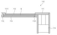
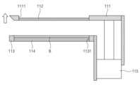
도 4에 도시된 바와 같이, 스테이지부(110)는 제1 브라켓(111), 제1 투명 플레이트(112), 제2 브라켓(113), 제2 투명 플레이트(114) 및 구동부(115)를 포함할 수 있다.As shown in FIG. 4 , the
제1 브라켓(111)은 제1 투명 플레이트(112)를 고정할 수 있다. 본 발명의 일 실시 예에서, 제1 브라켓(111)은 중간 영역에 배치되는 제1 개구부(1111)를 포함할 수 있다. 제1 브라켓(111)은 제1 개구부(1111)를 둘러싸는 제1 내측벽(미부호) 및 제1 내측벽(미부호)을 따라 형성된 제1 삽입 홈(미도시)을 포함할 수 있다. 제1 개구부(1111)는 제1 투명 플레이트(112)의 형상에 대응될 수 있다. 본 발명의 일 실시 예에서, 제1 개구부(1111)의 형상은 직사각형일 수 있다. 제1 삽입 홈(미도시)에 제1 투명 플레이트(112)의 가장 자리가 삽입될 수 있다. 제1 삽입 홈(미도시)에 제1 투명 플레이트(112)의 가장 자리가 삽입됨으로써, 제1 투명 플레이트(112)는 제1 브라켓(111)에 고정될 수 있다.The
제1 투명 플레이트(112)는 투명한 재질을 포함할 수 있다. 본 발명의 일 실시예에서, 제1 투명 플레이트(112)는 투명 유리일 수 있으나, 이에 한정되지 않고, 투명 플라스틱 등일 수 있다. 제1 투명 플레이트(112)는 기판(B)과 대응된 형상일 수 있다. 여기서, 대응된다는 것은 형상이 일치하거나 극히 유사한 경우를 의미할 수 있다. 본 발명의 일 실시 예에서, 제1 투명 플레이트(112)는 직사각형일 수 있으나, 이에 한정되지 않고, 정사각형, 원형 등의 다양한 형상일 수 있다. 제1 투명 플레이트(112)에 기판(B)이 배치될 수 있다. 이에 따라, 제1 투명 플레이트(112)에 기판(B)의 일면이 접촉될 수 있다.The first
제2 브라켓(113)은 제2 투명 플레이트(114)를 고정할 수 있다. 본 발명의 일 실시 예에서, 제2 브라켓(113)은 중간 영역에 배치되는 제2 개구부(1131)를 포함할 수 있다. 제2 브라켓(113)은 제2 개구부(1131)를 둘러싸는 제2 내측벽(미부호) 및 제2 내측벽(미부호)을 따라 형성된 제2 삽입 홈(미도시)을 포함할 수 있다. 제2 개구부(1131)는 제2 투명 플레이트(114)의 형상과 대응될 수 있다. 여기서, 형상과 대응된다는 것은 형상이 일치하거나 극히 유사한 경우를 의미할 수 있다. 본 발명의 일 실시 예에서, 제2 개구부(1131)의 형상은 직사각형일 수 있다. 제2 삽입 홈(미도시)에 제2 투명 플레이트(114)의 가장자리가 삽입될 수 있다. 제2 삽입 홈(미도시)에 제2 투명 플레이트(114)의 가장 자리가 삽입됨으로써, 제2 투명 플레이트(114)는 제2 브라켓(113)에 고정될 수 있다. 제2 브라켓(113)은 제1 브라켓(111)의 일측에 배치될 수 있다. 본 발명의 일 실시 예에서, 제2 브라켓(113)은 제1 브라켓(111)의 하측에 배치될 수 있다. 이에 따라, 제2 투명 플레이트(114)는 제1 투명 플레이트(112)의 하측에 배치될 수 있다.The
제2 투명 플레이트(114)는 투명한 재질을 포함할 수 있다. 제2 투명 플레이트(114)는 투명 유리일 수 있으나, 이에 한정되지 않고, 투명 플라스틱 등일 수 있다. 제2 투명 플레이트(114)는 기판(B)과 대응된 형상일 수 있다. 여기서, 대응된다는 것은 형상이 일치하거나 극히 유사한 경우를 의미할 수 있다. 본 발명의 일 실시 예에서, 제2 투명 플레이트(114)는 직사각형일 수 있으나, 이에 한정되지 않는다.The second
전술한 바와 같이, 제2 투명 플레이트(114)는 제1 투명 플레이트(112)의 하측에 배치될 수 있다. 제2 투명 플레이트(114)는 기판(B)의 하면과 접촉될 수 있다. 이에 따라, 기판(B)은 제1 투명 플레이트(112)와 제2 투명 플레이트(114) 사이에 배치될 수 있다. 기판(B)이 제1 및 제2 투명 플레이트(112, 114) 사이에 배치됨으로써, 기판은 스테이지 유닛(100)에 고정된 상태로 로딩될 수 있다.As described above, the second
구동부(115)는 제1 및 제2 투명 플레이트들(112, 114)이 서로 인접하게 배치되도록 제1 브라켓(111) 및 제2 브라켓(113) 중 적어도 어느 하나를 이동시킬 수 있다. 이에 따라, 제1 투명 플레이트(112) 및 제2 투명 플레이트(114) 중 적어도 어느 하나가 이동될 수 있다. 본 발명의 일 실시 예에서, 제2 브라켓(113)은 고정된 상태에 있고, 제1 브라켓(111)이 이동 가능한 상태에 있다. 이에 따라, 제1 브라켓(111)은 구동부(115)에 의해 상하 방향(Z축 방향)으로 이동될 수 있다. 본 발명의 일 실시 예에서, 구동부(115)는 유압 실린더일 수 있으나, 이에 한정되지 않고, 구동부(115)는 제1 브라켓(111) 및 제2 브라켓(113) 중 적어도 어느 하나를 이동시킬 수 있는 다양한 구성일 수 있다.The driving
회전 구동부(120)는 스테이지부(110)를 회전시켜, 스테이지부(110)에 로딩된 기판(B)을 회전시킬 수 있다. 본 발명의 일 실시예에서, 회전 구동부(120)는 스테이지부(110)를 180도 회전시켜, 기판(B)을 180도 회전시킬 수 있다. 이와 달리, 다른 실시예에서, 회전 구동부(120)는 스테이지부(110)를 90도 등 다양한 각도로 회전시킬 수 있다. 본 발명의 일 실시 예에서, 회전 구동부(120)는 모터일 수 있으나, 이에 한정되지 않고, 회전 구동부(120)는 스테이지부(110)를 회전시킬 수 있는 다양한 구성일 수 있다. 회전 구동부(120)는 제1 브라켓(111)의 끝단 및 제2 브라켓(113)의 끝단 중 적어도 어느 하나와 연결될 수 있다. 이에 따라, 회전 구동부(120)는 제1 브라켓(111) 및 제2 브라켓(112) 중 적어도 어느 하나를 회전시켜, 제1 및 제2 투명 플레이트(112, 114) 사이에 배치된 기판(B)을 회전시킬 수 있다.The
스테이지 지지부(130)는 스테이지부(110)를 지지할 수 있다. 스테이지 지지부(130)는 베이스 플레이트(131) 및 지지대들(132~134)을 포함할 수 있다. 베이스 플레이트(131)는 스테이지부(110)와 이격 배치될 수 있다. 본 발명의 일 실시 예에서, 베이스 플레이트(131)는 스테이지부(110)의 하측에 이격 배치될 수 있다. 지지대들(132~ 134)은 베이스 플레이트(131)의 길이 방향을 따라 배치될 수 있다. 본 발명의 일 실시 예에서, 지지대들(132~134)은 X축 방향을 따라 배치될 수 있다. 본 발명의 일 실시 예에서, 지지대들(132~134)은 3개의 지지대를 포함할 수 있다. 예를 들면, 지지대(132~134)들은 베이스 플레이트(131)의 일단에 배치된 제1 지지대(132), 베이스 플레이트(131)의 타단에 배치된 제2 지지대(133) 및 제1 지지대(132)와 제2 지지대(133) 사이에 배치된 제3 지지대(134)를 포함할 수 있다.The
제1 지지대(132)는 베이스 플레이트(131)의 일단으로부터 스테이지부(110)를 향해 연장될 수 있다. 제1 지지대(132)는 제1 및 제2 브라켓(111, 113)의 일단 중 적어도 어느 하나와 힌지 결합될 수 있다. 본 발명의 일 실시 예에서, 제1 지지대(132)는 제2 브라켓(113)의 일단과 힌지 결합될 수 있다.The
제2 지지대(133)는 베이스 플레이트(131)의 타단으로부터 스테이지부(110)를 향해 연장될 수 있다. 제2 지지대(133)의 상부에 회전 구동부(120)가 결합될 수 있다. 예를 들면, 제2 지지대(133)는 상부에 삽입 홀(미부호)을 가질 수 있다. 회전 구동부(120)는 제2 지지대(133)의 삽입 홀(미부호)에 삽입되어, 제2 지지대(133)의 상부에 결합될 수 있다.The
제3 지지대(134)는 베이스 플레이트(131)로부터 스테이지부(110)를 향해 연장될 수 있다. 제3 지지대(134)는 제1 및 제2 브라켓(111, 113)의 타단 중 적어도 어느 하나와 힌지 결합될 수 있다. 본 발명의 일 실시 예에서, 제3 지지대(134)는 제2 브라켓(113)의 타단과 힌지 결합될 수 있다. 이에 따라, 스테이지부(110)는 제1 및 제3 지지대(132, 134)에 지지된 상태에서 회전 구동부(120)에 의해 회전될 수 있다. 제1, 제2 및 제3 지지대(132~134)는 베이스 플레이트(131)로부터 연장된 길이가 동일할 수 있다.The
제1 연결 레일부(140)는 스테이지 지지부(130)의 아래에 배치될 수 있다. 본 발명의 일 실시 예에서, 제1 연결 레일부(140)는 베이스 플레이트(131)의 하부와 연결될 수 있다. 제1 연결 레일부(140)는 제1 이송 유닛(300)의 제1 가이드 레일부(310)와 연결될 수 있다. 도 1b에 도시된 바와 같이, 제1 연결 레일부(140)는 X축 방향과 나란하게 직선 배치된 2개의 제1 레일들(141, 142)을 포함할 수 있다. 제1 레일들(141, 142)의 각각은 Y축 방향으로 서로 이격하여 나란하게 배치될 수 있다. 제1 레일들(141, 142)의 각각은 제1 이송 유닛(300)의 제1 가이드 레일부(310)와 연결되어, 제1 가이드 레일부(310)를 따라 직선 왕복 운동할 수 있다. The first
촬상 유닛(200)은 스테이지 유닛(100)에 로딩된 기판(B)을 촬영할 수 있다. 촬상 유닛(200)은 스캔 카메라(210), 초점 조절 구동기(220), 변위 센서(230) 및 조명부(240)를 포함할 수 있다.The
스캔 카메라(210)는 기판(B)의 일면을 촬영하여 제1 영상 정보(I1)를 획득할 수 있다. 스캔 카메라(210)는 기판(B)의 타면을 촬영하여 제2 영상 정보(I2)를 획득할 수 있다. 이에 따라, 촬상 유닛(200)은 획득된 제1 및 제2 영상 정보(I1, I2)를 컨트롤러(500)로 전송할 수 있다. 본 발명의 일 실시 예에서 스캔 카메라(210)는 하나가 구비되나, 이에 한정되지 않고, 복수개가 구비될 수 있다. 여기서, 제1 영상 정보(I1)와 제2 영상 정보(I2)는 이미지일 수 있다.The
스캔 카메라(210)는 스테이지 유닛(100)의 일측에 배치될 수 있다. 본 발명의 일 실시 예에서, 스캔 카메라(210)는 스테이지부(110)의 상측에 배치되나, 이에 한정되지 않고, 스테이지부(110)의 하측, 우측 및 좌측 등에 배치될 수 있다.The
조명부(240)은 스캔 카메라(210)에 인접하게 배치될 수 있다. 본 발명의 일 실시 예에서, 조명부(240)는 스캔 카메라(210)와 인접한 위치에 이격 배치되나, 이에 한정되지 않고, 스캔 카메라(210)에 고정 설치될 수 있다. 조명부(240)은 기판(B)을 향해 빛을 조사할 수 있다. 이에 따라, 스캔 카메라(210)는 선명한 이미지를 획득할 수 있다. 조명부(240)는 LED 등과 같이 빛을 조사할 수 있는 광원을 포함할 수 있다.The
변위 센서(230)는 스캔 카메라(210)와 기판(B)과의 거리를 측정할 수 있다. 변위 센서(230)는 레이저 센서, 초음파 센서 등일 수 있다. 본 발명의 일 실시 예에서, 변위 센서(230)는 스캔 카메라(210)에 고정 설치될 수 있다. 변위 센서(230)는 발광부(미도시)와 수광부(미도시)를 포함할 수 있다. 발광부(미도시)는 기판(B)을 향해 레이저 광 등을 조사하고, 수광부(미도시)는 발광부(도시)에서 조사되어 기판(B)에서 반사된 레이저 광 등을 수광할 수 있다. 변위 센서(230)는 발광부(미도시)에서 조사된 빛이 수광부(미도시)에 도달하기까지의 시간을 측정하여 스캔 카메라(210)와 기판(B)과의 거리를 측정할 수 있다.The
초점 조절 구동기(220)는 변위 센서(230)에서 측정된 스캔 카메라(210)와 기판(B)과의 거리에 따라, 스캔 카메라(210)를 이동시킬 수 있다. 본 발명의 일 실시 예에서, 초점 조절 구동기(220)는 스캔 카메라(210)를 Z축 방향(상하 방향)으로 이동시킴으로써, 스캔 카메라(210)의 초점을 조절할 수 있다.The
제1 이송 유닛(300)은 스테이지 유닛(100)의 하측에 배치될 수 있다. 제1 이송 유닛(300)은 스테이지 유닛을 X축 방향으로 이동시킬 수 있는 다양한 구조로 이루어질 수 있다. 이에 따라, 스테이지 유닛(100)은 제1 이송 유닛(300)에 의해 X축 방향으로 이동될 수 있다. 본 발명의 일 실시 예에서, 제1 이송 유닛(300)은 스테이지 유닛(100)의 제1 연결 레일부(140)와 연결되는 제1 가이드 레일부(310) 및 스테이지 유닛(100)을 이동시키는 제1 이송 구동부(320)를 포함할 수 있다. 제1 이송 유닛(300)은 제2 이송 유닛(400)과 연결되는 제2 연결 레일부(330, 도 1c 참조)를 포함할 수 있다.The
제1 가이드 레일부(310)는 제1 연결 레일부(140)의 제1 연결 레일(141, 142)이 삽입되는 2개의 제1 레일 홈들(311, 312)을 포함할 수 있다. 예를 들면, 제1 가이드 레일부(310)은 X축 방향으로 길게 형성되는 제1 가이드 바디(미부호)와, 제1 가이드 바디(미부호)의 양측에 형성되는 제1 레일 홈들(311, 312)를 포함할 수 있다. 제1 레일 홈들(311, 312)의 각각은 X축 방향과 나란하게 배치될 수 있다. 제1 레일 홈들(311, 312)의 각각은 직선 형상일 수 있다. 제1 레일 홈들(311, 312)의 각각은 Y축 방향으로 서로 이격하여 나란하게 배치될 수 있다. 이하, 제1 레일 홈(311, 312)의 일단이 위치하는 지점을 제1 지점(340, 도 1b 참조)이라고 하고, 타단이 위치되는 지점을 제2 지점(350, 도 1b 참조)이라 지칭한다.The first
제1 이송 구동부(320)는 스테이지 유닛(100)을 제1 가이드 레일부(310)를 따라 이동시킬 수 있다. 예를 들면, 제1 이송 구동부(320)는 스테이지 유닛(100)을 제1 지점(340)과 제2 지점(350) 사이 구간에서 스테이지 유닛(100)을 직선 왕복 운동시킬 수 있다.The first
제2 연결 레일부(330)는 제1 가이드 레일부(310)의 아래에 배치될 수 있다. 제2 연결 레일부(330)는 제2 이송 유닛(400)의 제2 가이드 레일부(410)와 연결될 수 있다. 도 1c에 도시된 바와 같이, 제2 연결 레일부(330)는 Y축 방향과 나란하게 배치된 2개의 제2 레일들(331, 332)을 포함할 수 있다. 제2 레일들(331, 332)의 각각은 X축 방향으로 서로 이격하여 나란하게 배치될 수 있다. 제2 레일들(331, 332)의 각각은 제2 이송 유닛(400)의 제2 가이드 레일부(410)와 연결되어, 제2 가이드 레일부(410)를 따라 직선 왕복 운동할 수 있다.The second
제2 이송 유닛(400)은 스테이지 유닛(100)의 하측에 배치될 수 있다. 본 발명의 일 실시 예에서, 제2 이송 유닛(400)은 제1 이송 유닛(300)의 하측에 배치되나, 이에 한정되지 않고, 제1 이송 유닛(300)의 상측에 배치될 수 있다. 제2 이송 유닛(400)은 스테이지 유닛(100)을 Y축 방향으로 이동시킬 수 있는 구조로 이루어질 수 있다. 이에 따라, 스테이지 유닛(100)은 제2 이송 유닛(400)에 의해 Y축 방향으로 이동될 수 있다. 본 발명의 일 실시 예에서, 제2 이송 유닛(400)은 제1 이송 유닛(300)의 제2 연결 레일부(330)와 연결되는 제2 가이드 레일부(410) 및 제1 이송 유닛(300)을 이동시키는 제2 이송 구동부(미도시)을 포함할 수 있다.The
제2 가이드 레일부(410)는 Y축 방향으로 길게 형성되는 2개의 제2 가이드 바디들(미부호)와, 제2 가이드 바디들(미부호)의 각각에 형성되는 제2 레일 홈들(411, 412)를 포함할 수 있다. 제2 가이드 바디들(미부호)의 각각은 X축 방향으로 서로 이격하여 나란하게 배치될 수 있다.The second
제2 레일 홈들(411, 412)는 제2 연결 레일부(330)의 제2 레일들(331, 332)이 삽입될 수 있다. 제2 레일 홈들(411, 412)의 각각에 삽입된 제2 레일들(331, 332)은 제2 레일 홈들(411, 412)을 따라 Y축 방향으로 왕복 이동할 수 있다.The
제2 레일 홈들(411, 412)의 각각은 Y축 방향과 나란하게 배치될 수 있다. 제2 레일 홈들(411, 412)의 각각은 직선 형상일 수 있다. 제2 레일 홈들(411, 412)은 X축 방향으로 서로 이격하여 나란하게 배치될 수 있다. 이하, 제2 레일 홈(411, 412)의 일단이 위치하는 지점을 제3 지점(420)이라하고, 타단을 제4 지점(430)이라고 지칭한다.Each of the
제2 이송 구동부(미도시)는 제1 이송 유닛(300)을 제2 가이드 레일부(410)를 따라 이동시킬 수 있다. 제1 이송 유닛(300)이 제2 가이드 레일부(410)를 따라 Y축 방향으로 이동함으로써, 제1 이송 유닛(300) 상에 배치된 스테이지 유닛(100)도 Y축 방향으로 이동할 수 있다. 예를 들면, 제1 이송 구동부(320)는 제1 이송 유닛(300)과 스테이지 유닛(100)을 제3 지점(420)과 제4 지점(430) 사이 구간에서 스테이지 유닛(100)과 제1 이송 유닛(300)을 직선 왕복 운동시킬 수 있다.The second transfer driver (not shown) may move the
컨트롤러(500)는 스테이지 유닛(100), 촬상 유닛(200), 제1 이송 유닛(300) 및 제2 이송 유닛(400)을 제어할 수 있다. 본 발명의 일 실시 예에서, 컨트롤러(500)는 구동부(115), 회전 구동부(120), 초점 조절 구동기(220), 조명부(240), 제1 이송 구동부(320), 제2 이송 구동부(미도시) 등을 제어할 수 있다. 컨트롤러(500)는 촬상 유닛(200)으로부터 제1 영상 정보(I1) 및 제2 영상 정보(I2)를 수신할 수 있다. 컨트롤러(500)에 대한 자세한 사항은 후술한다.The
디스플레이 유닛(600)은 컨트롤러(500)로부터 전송받은 영상 정보들을 사용자에게 표시할 수 있다. 예를 들면, 디스플레이 유닛(600)은 제1 및 제2 영상 정보(I1, I2)가 오버랩된 이미지, 후술할 마크 위치 예측 정보(I3)를 표시할 수 있다. 디스플레이 유닛(600)은 터치 입력이 가능한 디스플레이 패널일 수 있으나, 이에 한정되는 것은 아니다.The
도 5는 도 3의 스테이지 유닛에 로딩되는 기판의 일면을 나타낸 도면이다. 도 6은 도 3의 스테이지 유닛에 로딩되는 기판의 타면을 나타낸 도면이다.FIG. 5 is a view showing one side of a substrate loaded on the stage unit of FIG. 3 . FIG. 6 is a view showing the other surface of a substrate loaded on the stage unit of FIG. 3 .
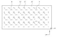
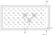
도 1, 도 5 및 도 6을 참조하면, 본 발명의 일 실시 예에 따른 스테이지 유닛(100)에 로딩되는 기판(B)은 전자 소자 영역들(A)을 포함할 수 있다. 전자 소자 영역들(A)의 각각은 일면(B1)에 표시된 마크(M), 일면(B1)에 표시된 기준 표식(E1) 및 일면(B1)에 대향된 타면(B2)에 표시된 소잉 표식(E2)을 포함할 수 있다.Referring to FIGS. 1, 5, and 6 , a substrate B loaded on the
본 발명의 일 실시 예에서, 기판(B)은 복수의 전자 소자 영역들을 포함할 수 있다. 이에 따라, 기판(B)의 일면(B1)에 복수의 마크들 및 복수의 기준 표식들이 표시되고, 기판(B)의 타면(B2)에 복수의 소잉(sawing) 표식들이 표시될 수 있다. 기준 표식들, 소잉 표식들 및 마크들은 레이저 식각 등을 통해 기판(B)의 일면(B1) 및 타면(B2)에 표시될 수 있다. 여기서, 전사 소자 영역(A)은 절단 부재(미도시)에 의해 절단될 때, 전자 소자가 될 수 있다.In one embodiment of the present invention, the substrate B may include a plurality of electronic device regions. Accordingly, a plurality of marks and a plurality of fiducial marks may be displayed on one surface B1 of the substrate B, and a plurality of sawing marks may be displayed on the other surface B2 of the substrate B. Reference marks, sawing marks, and marks may be marked on one surface B1 and the other surface B2 of the substrate B through laser etching or the like. Here, the transfer element region A may become an electronic element when cut by a cutting member (not shown).
기판(B)은 기판(B)을 관통하는 적어도 하나의 기준 홀(H1)을 포함할 수 있다. 본 발명의 일 실시 예에서, 기판(B)은 하나의 기준 홀(H1)을 포함하나, 기준 홀(H1)의 개수는 이에 한정되지 않는다. 기판(B)은 직사각형의 형상일 수 있으나, 이에 한정되는 것은 아니다.The substrate B may include at least one reference hole H1 penetrating the substrate B. In one embodiment of the present invention, the substrate B includes one reference hole H1, but the number of reference holes H1 is not limited thereto. The substrate B may have a rectangular shape, but is not limited thereto.
본 발명의 일 실시 예에서, 기준 표식(E1)은 도트(dot)일 수 있으나, 이에 한정되는 것은 아니다. 소잉 표식(E2)은 복수의 소잉 마크들을 포함할 수 있다. 소잉 마크들의 각각은 전자 소자 영역(A)의 꼭지점들의 각각에 배치될 수 있다. 본 발명의 일 실시 예에서, 소잉 표식(E2)은 십자 형상의 4개의 소잉 마크들을 포함할 수 있고, 전자 소자 영역(A)의 형상은 정사각형일 수 있으나, 이에 한정되지 않는다. 이에 따라, 4개의 소잉 마크들의 각각은 전자 소자 영역(A)의 4개의 꼭지점들의 각각에 배치될 수 있다. 마크(M)는 고객사의 심벌, 상표명 등일 수 있다. 마크(M)는 전자 소자 영역(A)의 중간 영역에 배치될 수 있다.In one embodiment of the present invention, the fiducial mark E1 may be a dot, but is not limited thereto. The sawing mark E2 may include a plurality of sawing marks. Each of the sawing marks may be disposed at each of vertices of the electronic device region A. In one embodiment of the present invention, the sawing mark E2 may include four sawing marks in a cross shape, and the shape of the electronic device region A may be a square, but is not limited thereto. Accordingly, each of the four sawing marks may be disposed at each of the four vertices of the electronic device region A. The mark (M) may be a symbol of a customer company, a brand name, or the like. The mark M may be disposed in a middle region of the electronic device region A.
도 7 내지 도 10는 도 1의 스테이지 유닛에 기판을 로딩하는 공정들을 나타낸 도면들이다. 도 11 내지 도 16는 도 1의 촬상 유닛이 제1 영상 정보 및 제2 영상 정보를 획득하는 공정들을 나타낸 도면들이다. 도 17 내지 도 18은 도 1의 스테이지 유닛에 로딩된 기판을 언 로딩하는 공정들을 나타낸 도면들이다.7 to 10 are diagrams illustrating processes of loading a substrate onto the stage unit of FIG. 1 . 11 to 16 are diagrams illustrating processes of acquiring first image information and second image information by the imaging unit of FIG. 1 . 17 to 18 are views illustrating processes of unloading a substrate loaded on the stage unit of FIG. 1 .
도 2, 도 5 내지 도 18을 참조하여, 본 발명의 일 실시 예에 따른 마크 위치 예측 장치(10)가 절단될 전자 소자 영역(A)의 마크(M)의 위치를 예측하는 공정들을 설명한다.2 and 5 to 18, processes for predicting the position of the mark M of the electronic device area A to be cut by the mark
도 2 및 도 7을 참조하면, 컨트롤러(500)는 제2 이송 유닛(400)의 제2 이송 구동부(미도시)를 제어하여, 제2 레일 홈들(411, 412)의 제3 지점(420)에 위치된 스테이지 유닛(100)과 제1 이송 유닛(300)을 제2 레일 홈들(411, 412)의 제4 지점(430)을 향해 이동시킬 수 있다. 이에 따라, 스테이지 유닛(100)은 제2 가이드 레일부(410)를 따라 제3 방향(D3)으로 이동할 수 있다. 여기서, 제3 방향(D3)은 제3 지점(420)에서 제4 지점(430)을 향한 방향일 수 있다. 그리고, 제3 방향(D3)은 Y축 방향과 평행할 수 있다.Referring to FIGS. 2 and 7 , the
도 2, 도 8 내지 도 10을 참조하면, 기판(B)은 기판 트랜스퍼(미도시)를 통해 제1 및 제2 투명 플레이트(112, 114) 중 어느 하나에 배치될 수 있다. 컨트롤러(500)는 제1 및 제2 투명 플레이트(112, 114) 중 나머지가 기판(B)과 접촉하도록 제1 및 제2 투명 플레이트(112, 114) 중 적어도 어느 하나를 이동시킬 수 있다.Referring to FIGS. 2 and 8 to 10 , the substrate B may be disposed on one of the first and second
예를 들면, 컨트롤러(500)는 스테이지 유닛(100)이 제2 레일 홈들(411, 412)의 제4 지점(430)에 위치한 후에 스테이지 유닛(100)의 구동부(115)를 제어하여, 제1 브라켓(111)을 상측으로 이동시킬 수 있다. 이에 따라, 서로 인접하게 배치된 제1 및 제2 브라켓(111, 113)은 이격 배치될 수 있다.For example, the
기판 트랜스퍼(미도시)는 기판(B)을 제2 투명 플레이트(114) 상에 배치시킬 수 있다. 이에 따라, 기판(B)의 하면은 제2 투명 플레이트(114)와 접촉될 수 있다. 컨트롤러(500)는 제2 투명 플레이트(114) 상에 기판(B)이 배치된 후, 구동부(115)를 제어하여 제1 브라켓(111)을 하측으로 하강시킬 수 있다. 제1 브라켓(111)이 하강함으로써, 제1 브라켓(111)에 고정된 제1 투명 플레이트(112)는 기판(B)의 상면과 접촉할 수 있다. 이에 따라, 기판(B)은 제1 및 제2 투명 플레이트(112, 114) 사이에 고정된 상태로 배치될 수 있다. 즉, 복수의 전자 소자 영역들을 포함하는 기판(B)이 스테이지 유닛(100)에 로딩될 수 있다.A substrate transfer (not shown) may place the substrate B on the second
도 2 및 도 11을 참조하면, 컨트롤러(500)는 기판(B)이 스테이지 유닛(100)에로딩된 후에 제2 이송 구동부(미도시)를 제어하여, 제2 레일 홈들(411, 412)의 제4 지점(440)에 위치된 스테이지 유닛(100)과 제1 이송 유닛(300)을 제3 지점(420)을 향해 이동시킬 수 있다. 이에 따라, 스테이지 유닛(100)은 제2 가이드 레일부(410)를 따라 제4 방향(D4)으로 이동할 수 있다. 여기서, 제4 방향(D4)은 제4 지점(430)에서 제3 지점(420)을 향한 방향일 수 있다. 그리고, 제4 방향(D4)은 Y축 방향과 평행할 수 있다.Referring to FIGS. 2 and 11 , the
도 2, 도 5 및 도 12를 참조하면, 컨트롤러(500)는 스테이지 유닛(100)이 제2 레일 홈들(411, 412)의 제3 지점(420)에 위치한 후에 제1 이송 구동부(320)를 제어하여, 스테이지 유닛(100)을 제1 레일 홈들(311, 312)의 제2 지점(350)을 향해 이동시킬 수 있다. 이에 따라, 스테이지 유닛(100)은 제1 가이드 레일부(310)를 따라 제1 방향(D1)으로 천천히 이동할 수 있다. 여기서, 제1 방향(D1)은 제1 지점(340)에서 제2 지점(350)을 향한 방향일 수 있다. 그리고, 제1 방향(D1)은 X축 방향과 평행할 수 있다.2, 5, and 12, the
촬상 유닛(200)은 제1 방향(D1)으로 천천히 이동하는 스테이지 유닛(100)에 로딩된 기판(B)의 상면을 촬영할 수 있다. 즉, 촬상 유닛(200)은 스테이지 유닛(100)에 로딩된 기판(B)의 전자 소자 영역(A)의 상면을 촬영할 수 있다. 이에 따라, 촬상 유닛(200)은 제1 영상 정보(I1)를 획득할 수 있다. 촬상 유닛(200)은 획득된 제1 영상 정보(I1)를 컨트롤러(500)로 전송할 수 있다. 스테이지 유닛(100)이 제1 방향(D1)으로 천천히 이동함으로써, 촬상 유닛(200)은 기판(B)의 전자 소자 영역(A)의 상면을 정밀하게 촬영할 수 있다. 이와 달리, 다른 실시 예에서, 촬상 유닛(200)은 정지 상태의 스테이지 유닛(100)에 로딩된 기판(B)의 전자 소자 영역(A)의 상면을 촬영할 수 있다.The
도 2, 도 6 및 도 13을 참조하면, 컨트롤러(500)는 스테이지 유닛(100)이 제1 레일 홈들(311, 312)의 제2 지점에 위치한 후에 회전 구동부(120)를 제어하여, 스테이지부(110)를 회전시킬 수 있다. 예를 들면, 컨트롤러(500)는 회전 구동부(120)를 제어하여, 제2 브라켓(113)을 180도 회전시킬 수 있다. 이에 따라, 기판(B)의 하면이 스테이지 유닛(100)의 상측에 배치된 촬상 유닛(200)에 노출될 수 있다. 다시 말하면, 컨트롤러(500)는 촬상 유닛(200)이 제1 영상 정보(I1) 및 제2 영상 정보(I2) 중 어느 하나를 획득한 후, 스테이지 유닛(100)이 기판(B)을 180도 회전하도록 제어할 수 있다.2, 6, and 13, the
도 2 및 도 14을 참조하면, 컨트롤러(500)는 스테이지부(110)를 회전시킨 후에 제1 이송 구동부(320)를 제어하여, 스테이지 유닛(100)을 제1 레일 홈들(311, 312)의 제1 지점(340)을 향해 이동시킬 수 있다. 이에 따라, 스테이지 유닛(100)은 제1 가이드 레일부(310)를 따라 제2 방향(D2)으로 천천히 이동할 수 있다. 여기서, 제2 방향(D2)은 제2 지점(350)에서 제1 지점(340)을 향한 방향일 수 있다. 그리고 제2 방향(D2)은 X축 방향과 평행할 수 있고, 제1 방향(D1, 도 12 참조)과는 반대 방향일 수 있다.Referring to FIGS. 2 and 14 , the
촬상 유닛(200)은 제2 방향(D2)으로 천천히 이동하는 스테이지 유닛(100)에 로딩된 기판(B)의 하면을 촬영할 수 있다. 즉, 촬상 유닛(200)은 스테이지 유닛(100)에 로딩된 기판(B)의 전자 소자 영역(A)의 하면을 촬영할 수 있다. 이에 따라, 촬상 유닛(200)은 제2 영상 정보(I2)를 획득할 수 있다. 촬상 유닛(200)은 획득된 제2 영상 정보(I2)를 컨트롤러(500)로 전송할 수 있다. 스테이지 유닛(100)이 제2 방향(D2)으로 천천히 이동함으로써, 촬상 유닛(200)은 기판(B)의 전자 소자 영역(A)의 하면을 정밀하게 촬영할 수 있다. 이와 달리, 다른 실시 예에서, 촬상 유닛(200)은 정지 상태의 스테이지 유닛(100)에 로딩된 기판(B)의 전자 소자 영역(A)의 하면을 촬영할 수 있다.The
도 2 및 도 15를 참조하면, 컨트롤러(500)는 스테이지 유닛(100)이 제1 레일 홈들(311, 312)의 제1 지점(340)에 위치한 후에 회전 구동부(120)를 제어하여, 스테이지부(110)를 회전시킬 수 있다. 예를 들면, 컨트롤러(500)는 회전 구동부(120)를 제어하여, 제2 브라켓(113)을 180도 회전시킬 수 있다.Referring to FIGS. 2 and 15 , the
도 2 및 도 16을 참조하면, 컨트롤러(500)는 제2 이송 구동부(미도시)를 제어하여, 스테이지 유닛(100)을 제4 지점(430)을 향해 이동시킬 수 있다. 이에 따라, 스테이지 유닛(100)은 제2 가이드 레일부(410)를 따라 제3 방향(D3)으로 이동될 수 있다.Referring to FIGS. 2 and 16 , the
도 2, 도 17 및 도 18을 참조하면, 컨트롤러(500)는 스테이지 유닛(100)이 제2 레일 홈들(411, 412)의 제4 지점(430)에 위치한 후에 구동부(115)를 제어하여, 제1 브라켓(111)을 상측으로 이동할 수 있다. 이에 따라, 제1 및 제2 투명 플레이트(112, 114)에 의해 스테이지 유닛(100)에 고정된 기판(B)은 고정 해제될 수 있다. 기판 트랜스퍼(미도시)는 제2 투명 플레이트(114) 상에 배치된 기판(B)을 꺼낼 수 있다. 이에 따라, 스테이지 유닛(100)에 로딩된 기판(B)은 스테이지 유닛(100)으로부터 언 로딩될 수 있다. 기판 트랜스퍼(미도시)는 스테이지 유닛(100)으로부터 기판(B)을 언 로딩한 후, 새로운 기판을 제2 투명 플레이트(114) 상에 배치할 수 있다.2, 17 and 18, the
도 19은 도 1의 촬상 유닛이 획득한 제1 영상 정보(I1)와 제2 영상 정보(I2)를 오버랩한 이미지 나타낸 도면이다. 도 20은 도 19의 이미지에 소잉 라인이 표시된 상태를 나타낸 도면이다.FIG. 19 is a diagram showing overlapped images of first image information I1 and second image information I2 acquired by the imaging unit of FIG. 1 . FIG. 20 is a view showing a state in which a sawing line is displayed in the image of FIG. 19 .
도 2, 도 19 및 도 20을 참조하면, 컨트롤러(500)는 촬상 유닛(200)으로부터 획득한 제1 및 제2 영상 정보(I1, I2)를 수신할 수 있다. 여기서, 제1 영상 정보(I1)는 기판(B)의 일면(B1, 도 5 참조)을 촬영한 이미지이다. 제2 영상 정보(I2)는 기판(B)의 타면(B2, 도 6 참조)을 촬영한 이미지이다.Referring to FIGS. 2 , 19 and 20 , the
컨트롤러(500)는 제2 영상 정보(I2)에 포함된 소잉 표식(E2)를 이용하여, 소잉 라인(L1)을 추출할 수 있다. 본 발명의 일 실시 예에서, 컨트롤러(500)는 수신한 제1 영상 정보(I1)에 포함된 기판(B)의 기준 홀(H1)의 위치 및 제2 영상 정보(I2)에 포함된 기판(B)의 기준 홀(H1)의 위치를 이용하여, 제1 영상 정보(I1)와 제2 영상 정보(I2)를 오버랩할 수 있다.The
예를 들면, 컨트롤러(500)는 제2 영상 정보(I2)에 포함된 기준 홀(H1)에 대한 소잉 표식들의 각각(E2)의 위치를 X, Y 좌표로 산출할 수 있다. 컨트롤러(500)는 제1 영상 정보(I1)에 포함된 기준 홀(H1)에 대한 기준 표식들의 각각(E2)의 위치를 X, Y 좌표로 산출할 수 있다. 본 발명의 일 실시 예에서, 소잉 표식(E2)의 X, Y 좌표는 소잉 마크들의 각각의 중심 점에 관한 X, Y 좌표를 포함할 수 있다. 기준 표식(E1)의 X, Y 좌표는 기준 표식(E1)의 중심 점에 관한 것일 수 있다.For example, the
컨트롤러(500)는 산출된 소잉 표식들의 각각(E2)의 X, Y 좌표와 산출된 기준 표식들의 각각(E1)의 X, Y 좌표를 이용하여, 소잉 표식들의 각각(E2)을 제1 영상 정보(I1)에 오버랩할 수 있다. 이에 따라, 소잉 표식들은 제1 영상 정보(I1)에 표시될 수 있다.The
컨트롤러(500)는 제1 영상 정보(I1)와 제2 영상 정보(I2)를 오버랩한 후, 소잉 표식(E2)을 이용하여, 소잉 라인(L1)을 추출할 수 있다. 즉, 컨트롤러(500)는 소잉 표식(E2)으로부터 소잉 라인(L1)을 추출하여 제1 영상 정보(I1)에 표시할 수 있다. 여기서, 소잉 라인(L1)은 소잉 표식(E2)에 포함된 복수의 소잉 마크들을 직접 연결한 라인을 의미할 수 있다. 소잉 라인(L1)은 전자 소자 영역(A)의 경계 라인을 의미할 수 있고, 블레이드 등의 절단 부재(미도시)는 소잉 라인(L1)을 따라 전자 소자 영역(A)을 절단할 수 있다. 기준 표식(E1)과 마크(M)는 소잉 라인(L1) 내에 위치할 수 있다.The
이와 달리, 다른 실시 예에서, 컨트롤러(500)는 소잉 표식(E2)의 X, Y 좌표를 이용하여, 소잉 라인(L1)을 추출할 수 있다. 컨트롤러(500)는 수신한 제1 영상 정보(I1)에 포함된 기판(B)의 기준 홀(H1)의 위치와 제2 영상 정보(I2)에 포함된 기판(B)의 기준 홀(H1)의 위치를 이용하여, 제1 영상 정보(I1)와 소잉 라인(L1)이 추출된 제2 영상 정보(I2)를 오버랩할 수 있다. 즉, 컨트롤러(500)는 소잉 라인(L1)을 추출한 후, 기준 홀(H1)에 대한 소잉 라인들의 각각(L1)의 X, Y 좌표 및 기준 홀(H1)에 대한 기준 표식들의 각각(E1)의 X, Y 좌표를 산출할 수 있다. 컨트롤러(500)는 소잉 라인들의 각각(L1)의 X, Y 좌표 및 기준 표식들의 각각(E1)의 X, Y 좌표를 이용하여, 소잉 라인들을 제1 영상 정보(I1)에 오버랩할 수 있다. 이에 따라, 소잉 라인들은 제1 영상 정보(I1)에 표시되거나, 기준 표식들이 제2 영상 정보(I2)에 표시될 수 있다.Unlike this, in another embodiment, the
도 21는 도 20의 EA1 부분을 확대한 확대도이다. 도 22은 도 20의 EA2 부분을 확대한 확대도이다. 도 23는 도 20의 EA3 부분을 확대한 확대도이다. 도 24는 도 2의 디스플레이 유닛에 마크 위치 예측 정보를 표시한 도면이다.FIG. 21 is an enlarged view of a portion EA1 of FIG. 20 . FIG. 22 is an enlarged view of part EA2 of FIG. 20 . FIG. 23 is an enlarged view of a portion EA3 of FIG. 20 . 24 is a diagram displaying mark position prediction information on the display unit of FIG. 2 .
도 2, 도 21 내지 도 24를 참조하면, 컨트롤러(500)는 소잉 라인(L1)과 기준 표식(E1)을 이용하여, 기준 표식(E1)과 소잉 라인(L1) 간의 이격 거리를 산출할 수 있다. 본 발명의 일 실시 예에서, 컨트롤러(500)는 기준 표식(E1) 및 기준 표식(E1)으로부터 제1 방향(D'1)의 소잉 라인(L1)과의 제1 이격 거리를 산출할 수 있다. 컨트롤러(500)는 기준 표식(E1) 및 기준 표식(E1)으로부터 제1 방향(D'1)과 상이한 제2 방향(D'2)의 소잉 라인(L1)과의 제2 이격 거리를 산출할 수 있다. 본 발명의 일 실시예에서, D'1 및 D'2는 서로 직교할 수 있다. D'1은 X축에 평행할 수 있고, D'2는 Y축에 평행할 수 있다. D'1은 D1(도 12 참조) 및는 D2(도 13 참조) 중 어느 하나와 동일한 방향일 수 있다. D'2는 D3(도 7 참조) 및 D4(도 11 참조) 중 어느 하나와 동일한 방향일 수 있다.2 and 21 to 24, the
컨트롤러(500)는 기 설정된 기준 거리와 산출된 이격 거리의 대응 여부로부터 소잉 라인(L1)을 따라 절단될 전자 소자 영역들의 각각(A)에 표시된 마크(M)의 위치를 예측할 수 있다. 여기서, 기준 거리와 이격 거리가 대응된다는 것은 이격 거리가 기준 거리에 일치하는 경우뿐만 아니라 이격 거리가 기준 거리의 오차 범위 내인 경우를 포함하는 의미이다. 기 설정된 기준 거리는 기준 표식(E1) 및 기준 표식(E1)으로부터 제1 방향(D'1)의 소잉 라인(L1)과의 제1 기준 거리를 포함할 수 있다. 기 설정된 기준 거리는 기준 표식(E1) 및 기준 표식(E1)으로부터 제2 방향(D'2)의 소잉 라인(L1)과의 제2 기준 거리를 포함할 수 있다. 이에 따라, 컨트롤러(500)는 제1 기준 거리와 제1 이격 거리의 대응 여부 및 제2 기준 거리와 제2 이격 거리의 대응 여부를 판단할 수 있다.The
컨트롤러(500)는 산출된 이격 거리가 기준 거리에 대응될 때, 소잉 라인(L1)을 따라 절단될 전자 소자 영역들의 각각(A)에 표시된 마크(M)가 기 설정된 기준 영역(SA)에 위치된다고 예측할 수 있다.When the calculated separation distance corresponds to the reference distance, the
도 2 및 도 21를 참조하면, 컨트롤러(500)는 제1 이격 거리(X1)가 제1 기준 거리에 대응되고, 제2 이격 거리(Y1)가 제2 기준 거리에 대응될 때, 소잉 라인(L1)을 따라 절단될 전자 소자 영역들의 각각(A)에 표시된 마크(M)가 기 설정된 기준 영역(SA)에 위치된다고 예측할 수 있다.2 and 21, the
컨트롤러(500)는 산출된 이격 거리가 기준 거리에 대응되지 않을 때, 소잉 라인(L1)을 따라 절단될 전자 소자 영역들의 각각(A)에 표시된 마크(M)가 기 설정된 기준 영역(SA)을 벗어난다고 예측할 수 있다.When the calculated separation distance does not correspond to the reference distance, the
도 2 및 도 22을 참조하면, 컨트롤러(500)는 제1 이격 거리(X2)가 제1 기준 거리(X0)에 대응되나, 제2 이격 거리(Y2)가 제2 기준 거리(Y0)에 대응되지 않을 때, 소잉 라인(L1)을 따라 절단될 전자 소자 영역들의 각각(A)에 표시된 마크(M)가 기 설정된 기준 영역(SA)을 벗어난다고 예측할 수 있다.2 and 22 , the
도 2 및 도 23을 참조하면, 컨트롤러(500)는 제2 이격 거리(Y3)가 제2 기준 거리(Y0)에 대응되나, 제1 이격 거리(X3)가 제1 기준 거리(X0)에 대응되지 않을 때, 소잉 라인(L1)을 따라 절단될 전자 소자 영역들의 각각(A)에 표시된 마크(M)가 기 설정된 기준 영역(SA)을 벗어난다고 예측할 수 있다.2 and 23 , the
컨트롤러(500)는 마크 위치 예측 결과 정보(I3)를 디스플레이 유닛(600)으로 전송할 수 있다. 디스플레이 유닛(600)은 마크 위치 예측 결과 정보(I3)를 사용자에 표시할 수 있다. 이에 따라, 사용자는 전자 소자 영역(A)이 절단될 때, 마크(M)의 위치가 불량인 전자 소자 영역(AF)을 신속하게 파악할 수 있다.The
도 20 및 도 24를 참조하면, 마크(M)의 위치가 기 설정된 기준 영역(SA)를 벗어난 전자 소자 영역(AF)은 마크(M)의 위치가 기 설정된 기준 영역(SA)에 위치한 전자 소자 영역(A)과 상이하게 표시될 수 있다.Referring to FIGS. 20 and 24 , the electronic element area AF in which the position of the mark M is out of the reference area SA is the electronic element in which the position of the mark M is located in the reference area SA. It may be displayed differently from area (A).
도 25은 본 발명의 일 실시 예에 따른 마크 위치 예측 장치의 일부 구성을 나타낸 개략도이다. 도 26은 본 발명의 일 실시 예에 따른 마크 위치 예측 장치를 나타낸 블록도이다.25 is a schematic diagram showing some configurations of a mark position predicting device according to an embodiment of the present invention. 26 is a block diagram illustrating an apparatus for predicting a position of a mark according to an embodiment of the present invention.
도 25 및 도 26를 참조하면, 본 발명의 일 실시 예에 따른 마크 위치 예측 장치(10a)는 스테이지 유닛(100a), 촬상 유닛(200a), 제1 이송 유닛(300a), 컨트롤러(500a) 및 디스플레이 유닛(600)을 포함할 수 있다. 설명의 간결함을 위해, 도 1 내지 도 3을 참조하여 설명한 예와 실질적으로 동일한 구성요소에 대한 설명은 생략한다.25 and 26, the mark
스테이지 유닛(100a)은 기판(B)을 로딩할 수 있다. 스테이지 유닛(100a)은 스테이지부(110a), 회전 구동부(120), 스테이지 지지부(130) 및 제1 연결 레일부(140)를 포함할 수 있다.The
스테이지부(110a)는 제1 브라켓(111a), 제1 투명 플레이트(112), 제2 브라켓(113a), 제2 투명 플레이트(114) 및 구동부(115a)를 포함할 수 있다.The
제2 브라켓(113a)은 제1 브라켓(111a)의 일측에 배치될 수 있다. 본 발명의 일 실시 예에서, 제1 및 제2 브라켓(111a, 113a)은 X축 방향을 따라 나란하게 배치될 수 있다. 제1 및 제2 브라켓(111a, 113a)은 서로 힌지 결합될 수 있다.The
구동부(115a)는 제1 및 제2 투명 플레이트(112, 114)가 서로 대향되게 배치되도록 제1 및 제2 브라켓(111a, 113a) 중 어느 하나를 회전시킬 수 있다. 본 발명의 일 실시 예에서, 구동부(115a)는 제2 브라켓(113a)과 힌지 결합된 제1 브라켓(111a)을 180도 회전시킬 수 있다. 제1 브라켓(111a)이 180도 회전됨으로써, 제1 및 제2 투명 플레이트(112, 114)는 서로 대향되게 배치될 수 있다. 본 발명의 일 실시 예에서, 구동부(115a)는 회전 모터일 수 있다.The
촬상 유닛(200a)은 스테이지 유닛(100a)에 로딩된 기판(B)을 촬영할 수 있다. 촬상 유닛(200a)은 스테이지부(110a)의 일측에 배치되는 제1 스캔 카메라(211a)와, 스테이지부(110a)의 타측에 배치되는 제2 스캔 카메라(212a)와, 스테이지부(110a)의 일측에 배치된 제1 조명부(241a)와, 스테이지부(110a)의 타측에 배치된 제2 조명부(242a)를 포함할 수 있다. 본 발명의 일 실시 예에서, 제1 스캔 카메라(211a)와 제1 조명부(241a)는 스테이지부(110a)의 상측에 배치되고, 제2 스캔 카메라(212a)와 제2 조명부(242a)는 스테이지부(110a)의 하측에 배치될 수 있다.The
제1 스캔 카메라(211a)는 스테이지부(110a)에 로딩된 기판(B)의 상면을 촬영하여 제1 영상 정보(I1)를 획득할 수 있다. 제2 스캔 카메라(212a)는 스테이지부(110a)에 로딩된 기판(B)의 하면을 촬영하여 제2 영상 정보(I2)를 획득할 수 있다.The
제1 조명부(241a)는 제1 스캔 카메라(211a)와 인접하게 배치될 수 있다. 제1 조명부(241a)는 기판(B)의 상면을 향해 빛을 조사할 수 있다. 이에 따라, 제1 스캔 카메라(211a)는 선명한 이미지를 획득할 수 있다.The
제2 조명부(242a)는 제2 스캔 카메라(212a)와 인접하게 배치될 수 있다. 제2 조명부(242a)는 기판(B)의 하면을 향해 빛을 조사할 수 있다. 이에 따라, 제2 스캔 카메라(212a)는 선명한 이미지를 획득할 수 있다.The
제1 이송 유닛(300a)은 스테이지 유닛(100a)을 X축 방향으로 이동시킬 수 있다. 제1 이송 유닛(300a)은 스테이지 유닛(100)의 하측에 배치될 수 있다. 본 발명의 일 실시 예에서, 제1 이송 유닛(300a)은 스테이지 유닛(100a)의 제1 연결 레일부(140)과 연결되는 제1 가이드 레일부(310) 및 스테이지 유닛(100a)을 이동시키는 제1 이송 구동부(미도시)를 포함할 수 있다.The
컨트롤러(500a)는 스테이지 유닛(100a), 촬상 유닛(200a) 및 제1 이송 유닛(300a)을 제어할 수 있다. 예를 들면, 컨트롤러(500a)는 스테이지 유닛(100a)은 회전 구동부(120) 및 구동부(115a)를 제어할 수 있다. 컨트롤러(500)는 촬상 유닛(200a)의 제1 조명부(241a)와 제2 조명부(242a)를 제어할 수 있다. 컨트롤러(500a)는 제1 이송 유닛(300a)의 제1 이송 구동부(미도시)를 제어할 수 있다.The
디스플레이 유닛(600)은 컨트롤러(500a)로부터 전송받은 제1 및 제2 영상 정보를 오버랩한 이미지, 마크 위치 예측 정보(I3) 등을 사용자에게 표시할 수 있다.The
도 27는 도 25의 촬상 유닛이 획득한 제1 영상 정보와 제2 영상 정보를 오버랩한 이미지에 소잉 라인과 에지 라인이 표시된 상태를 나타낸 도면이다. 설명의 간결함을 위해, 도 19 내지 도 20을 참조하여 설명한 예와 실질적으로 동일한 구성요소에 대한 설명은 생략한다.FIG. 27 is a diagram illustrating a state in which sawing lines and edge lines are displayed on an image obtained by overlapping first image information and second image information acquired by the imaging unit of FIG. 25 . For brevity of description, descriptions of components substantially the same as those of the example described with reference to FIGS. 19 to 20 will be omitted.
도 25 및 도 27를 참조하면, 컨트롤러(500a)는 촬상 유닛(200a)으로부터 획득한 제1 및 제2 영상 정보(I1, I2)를 수신할 수 있다.Referring to FIGS. 25 and 27 , the
컨트롤러(500a)는 제2 영상 정보(I2)에 포함된 소잉 표식(E2)을 이용하여, 소잉 라인(L1)을 추출할 수 있다. 컨트롤러(500a)는 수신한 제1 영상 정보(I1)에 포함된 기판(B)의 기준 홀(H1)의 위치 및 제2 영상 정보(I2)에 포함된 기판(B)의 기준 홀(H1)의 위치를 이용하여, 제1 영상 정보(I1)와 제2 영상 정보(I2)를 오버랩할 수 있다.The
본 발명의 일 실시 예에서, 컨트롤러(500a)는 제1 영상 정보(I1)와 제2 영상 정보(I2)를 오버랩한 후, 소잉 라인(L1)을 추출할 수 있다. 블레이드 등의 절단 부재(미도시)는 소잉 라인(L1)을 따라 전자 소자 영역(A)을 절단할 수 있다. 절단 부재(미도시)는 소정의 두께를 가질 수 있다. 이에 따라, 절단 부재(미도시)에 의해 절단된 전자 소자 영역(A)의 에지 라인(L2)은 소잉 라인(L1)과 일치하지 않을 수 있다.In an embodiment of the present invention, the
컨트롤러(500a)는 소잉 라인(L1)을 추출한 후, 소잉 라인(L1)을 따라 전자 소자 영역을 절단하는 절단 부재(미도시)의 두께를 보상하여 에지 라인(L2)을 추출할 수 있다. 컨트롤러(500a)는 제1 영상 정보(I1)에 포함된 기판(B)의 기준 홀(H1)의 위치와 제2 영상 정보(I2)에 포함된 기판(B)의 기준 홀(H1)의 위치를 이용하여, 제1 영상 정보(I1)와 에지 라인(L2)이 추출된 제2 영상 정보(I2)를 오버랩할 수 있다.After extracting the sawing line L1, the
도 28은 도 27의 EA4 부분을 확대한 확대도이다. 도 29은 도 27의 EA5 부분을 확대한 확대도이다. 도 30은 도 27의 EA6 부분을 확대한 확대도이다. 도 31는 도 26의 디스플레이 유닛에 마크 위치 예측 정보를 표시한 도면이다.FIG. 28 is an enlarged view of a portion EA4 of FIG. 27 . FIG. 29 is an enlarged view of a portion EA5 of FIG. 27 . FIG. 30 is an enlarged view of part EA6 of FIG. 27; FIG. 31 is a diagram displaying mark position prediction information on the display unit of FIG. 26 .
도 26, 도 28 내지 도 31를 참조하면, 컨트롤러는 에지 라인(L2)과 기준 표식(E1)을 이용하여, 기준 표식(E1)과 에지 라인(L2) 간의 이격 거리를 산출할 수 있다. 본 발명의 일 실시 예에서, 컨트롤러(500a)는 기준 표식(E1) 및 기준 표식(E1)으로부터 제1 방향(D'1)의 에지 라인(L2)과의 제1 이격 거리를 산출할 수 있다. 컨트롤러(500a)는 기준 표식(E1) 및 기준 표식(E1)으로부터 제1 방향(D'1)과 상이한 제2 방향(D'2)의 에지 라인(L2)과의 제2 이격 거리를 산출할 수 있다.Referring to FIGS. 26 and 28 to 31 , the controller may calculate the separation distance between the reference mark E1 and the edge line L2 using the edge line L2 and the reference mark E1. In one embodiment of the present invention, the
컨트롤러(500a)는 기 설정된 기준 거리와 산출된 이격 거리의 대응 여부로부터 소잉 라인(L1)을 따라 절단될 전자 소자영역들의 각각(A)에 표시된 마크(M)의 위치를 예측할 수 있다.The
컨트롤러(500a)는 산출된 이격 거리가 기준 거리에 대응될 때, 소잉 라인(L1)을 따라 절단될 절단될 전자 소자 영역들의 각각(A)에 표시된 마크(M)가 기 설정된 기준 영역(SA)에 위치된다고 예측할 수 있다.When the calculated separation distance corresponds to the reference distance, the
도 26 및 도 28을 참조하면, 컨트롤러(500a)는 제1 이격 거리(X4)가 제1 기준 거리에 대응되고, 제2 이격 거리(Y4)가 제2 기준 거리에 대응될 때, 소잉 라인(L1)을 따라 절단될 전자 소자 영역들의 각각(A)에 표시된 마크(M)가 기 설정된 기준 영역(SA)에 위치된다고 예측할 수 있다.Referring to FIGS. 26 and 28 , the
도 26 및 도 29을 참조하면, 컨트롤러(500a)는 제1 이격 거리(X5)가 제1 기준 거리(X'0)에 대응되나, 제2 이격 거리(Y5)가 제2 기준 거리(Y'0)에 대응되지 않을 때, 소잉 라인(L1)을 따라 절단될 전자 소자 영역들의 각각(A)에 표시된 마크(M)가 기 설정된 기준 영역(SA)을 벗어난다고 예측할 수 있다.Referring to FIGS. 26 and 29 , the
도 26 및 도 30을 참조하면, 컨트롤러(500a)는 제2 이격 거리(Y6)가 제2 기준 거리(Y'0)에 대응되나, 제1 이격 거리(X6)가 제1 기준 거리(X'0)에 대응되지 않을 때, 소잉 라인(L1)을 따라 절단될 전자 소자 영역들의 각각(A)에 표시된 마크(M)가 기 설정된 기준 영역(SA)을 벗어난다고 예측할 수 있다.Referring to FIGS. 26 and 30 , the
컨트롤러(500)는 마크 위치 예측 결과 정보(I3)를 디스플레이 유닛(600)으로 전송할 수 있다. 디스플레이 유닛(600)은 마크 위치 예측 결과 정보(I3)를 사용자에 표시할 수 있다.The
도 26, 도 27 및 도 31를 참조하면, 마크(M)의 위치가 기 설정된 기준 영역(SA)를 벗어난 전자 소자 영역(AF)은 마크(M)의 위치가 기 설정된 기준 영역(SA)에 위치한 전자 소자 영역(A)과 상이하게 표시될 수 있다.Referring to FIGS. 26, 27, and 31 , the electronic device area AF in which the position of the mark M is out of the reference area SA is set in the reference area SA where the position of the mark M is set. It may be displayed differently from the located electronic device area A.
도 32은 도 2의 촬상 유닛이 획득한 제1 영상 정보와 제2 영상 정보를 오버랩한 이미지를 나타낸 도면이다. 설명의 간결함을 위해, 도 1a 내지 도 4, 도 19 및 도 20을 참조하여 설명한 예와 실질적으로 동일한 구성요소에 대한 설명은 생략한다.FIG. 32 is a diagram illustrating an overlapping image of first image information and second image information acquired by the imaging unit of FIG. 2 . For brevity of description, descriptions of components substantially the same as those of the examples described with reference to FIGS. 1A to 4, 19, and 20 are omitted.
도 1a 내지 도 4 및 도 32을 참조하면, 스테이지 유닛(100)에 로딩되는 기판(B)은 적어도 하나의 기준 홀(H1)을 포함할 수 있다. 기판(B)은 복수의 전자 소자 영역들을 포함할 수 있다. 전자 소자 영역들의 각각(A)은 일면에 표시된 마크(M), 일면에 표시된 기준 표식(E1) 및 일면에 대향된 타면에 표시된 소잉 표식(E2)를 포함할 수 있다.Referring to FIGS. 1A to 4 and 32 , the substrate B loaded on the
본 발명의 일 실시 예에서, 스테이지 유닛(100)은 촬상 유닛(200)이 제1 영상 정보(I1) 및 제2 영상 정보(I2) 중 어느 하나를 획득한 후, 기판(B)을 180도 회전시킬 수 있다.In one embodiment of the present invention, the
컨트롤러(500)는 촬상 유닛(200)으로부터 획득한 제1 및 제2 영상 정보(I1, I2)를 수신할 수 있다. 컨트롤러(500)는 제1 영상 정보(I1) 및 제2 영상 정보(I2)를 이용하여, 기준 표식(E1)의 X, Y 좌표 및 소잉 표식(E2)의 X, Y 좌표를 산출할 수 있다. 여기서, 기준 표식(E1)의 X, Y 좌표는 제1 영상 정보(I1)에 포함된 기준 홀(H1)을 기준으로 산출할 수 있다. 소잉 표식(E2)의 X, Y 좌표는 제2 영상 정보(I2)에 포함된 기준 홀(H1)을 기준으로 산출할 수 있다.The
본 발명의 일 실시 예에서, 기준 홀(H1)은 X-Y축 상의 원점으로 설정될 수 있다. 컨트롤러(500)는 기준 홀(H1)을 기준으로 한 기준 표식(E1)의 위치를 X, Y 좌표로 산출할 수 있다. 컨트롤러(500)는 기준 홀(H1)을 기준으로 한 소잉 표식(E2)의 위치를 X, Y 좌표로 산출할 수 있다. 소잉 표식(E2)는 복수의 소잉 마크들을 포함할 수 있다. 컨트롤러(500)는 기준 홀(H1)을 기준으로 소잉 마크들의 각각에 대한 X, Y 좌표를 산출할 수 있다.In one embodiment of the present invention, the reference hole H1 may be set as an origin on the X-Y axes. The
컨트롤러(500)는 제1 영상 정보(I1)에 포함된 기준 홀(H1)의 위치와 제2 영상 정보(I2)에 포함된 기준 홀(H1)의 위치를 이용하여, 제1 영상 정보(I1)와 제2 영상 정보(I2)를 오버랩할 수 있다. 이에 따라, 소잉 표식들은 제1 영상 정보(I1)에 표시되거나, 기준 표식들이 제2 영상 정보(I2)에 표시될 수 있다.The
도 33는 도 32의 EA7 부분을 확대한 확대도이다. 도 34은 도 32의 EA8 부분을 확대한 확대도이다. 도 35은 도 32의 EA9 부분을 확대한 확대도이다. 도 36은 도 2의 디스플레이 유닛에 마크 위치 예측 결과 정보를 표시한 도면이다.FIG. 33 is an enlarged view of a portion EA7 of FIG. 32; FIG. 34 is an enlarged view of a portion EA8 of FIG. 32; FIG. 35 is an enlarged view of part EA9 of FIG. 32; 36 is a diagram showing mark position prediction result information displayed on the display unit of FIG. 2 .
도 2, 도 32 내지 도 36를 참조하면, 컨트롤러(500)는 산출된 기준 표식(E1)의 X, Y 좌표와 소잉 표식(E2)의 X, Y 좌표를 이용하여, 기준 표식(E1) 및 소잉 표식(E2) 간의 X, Y 거리를 산출할 수 있다. 여기서 X 거리는 기준 표식(E1)의 X 좌표와 소잉 표식(E2)의 X 좌표의 차의 절대값이고, Y 거리는 기준 표식(E1)의 Y 좌표와 소잉 표식(E2)의 Y 좌표의 차의 절대값이다,2 and 32 to 36, the
컨트롤러(500)는 기 설정된 기준 거리와 산출된 X, Y 거리의 대응 여부를 판단할 수 있다. 컨트롤러(500)는 기준 거리와 X, Y 거리의 대응 여부로부터 절단될 상기 전자 소자 영역들의 각각(A)에 표시된 마크(M)의 위치를 예측할 수 있다. 여기서, 기준 거리와 X, Y 거리가 대응된다는 것은 X, Y 거리가 기준 거리에 일치하는 경우뿐만 아니라, X, Y 거리가 기준 거리의 오차 범위 내인 경우를 포함하는 의미이다. 기준 거리는 X 거리에 대응되는 제1 기준 거리와 Y 거리에 대응되는 제2 기준 거리를 포함할 수 있다.The
도 2 및 도 33을 참조하면, 기준 표식(E1) X, Y 좌표는 (x'7, y'7)이고, 기준 표식(E1)과 인접한 소잉 표식(E2)의 소잉 마크의 X, Y 좌표는 (x''7, y''7)이다. 이에 따라, 컨트롤러(500)에서 산출된 X 거리는 |x'7-x''7|이고, 컨트롤러(500)에서 산출된 Y 거리는 |y'7-y''7|일 수 있다.2 and 33, the X and Y coordinates of the reference mark E1 are (x'7, y'7), and the X and Y coordinates of the sawing mark of the sawing mark E2 adjacent to the reference mark E1. is (x''7, y''7). Accordingly, the X distance calculated by the
컨트롤러(500)는 X, Y 거리(X7, Y7)가 기준 거리에 대응될 때, 절단될 전자 소자 영역들의 각각(A)에 표시된 마크(M)가 기 설정된 기준 영역(SA)에 위치된다고 예측할 수 있다.When the X and Y distances X7 and Y7 correspond to the reference distance, the
도 2 및 도 34을 참조하면, 기준 표식(E1) X, Y 좌표는 (x'8, y'8)이고, 기준 표식(E1)과 인접한 소잉 표식(E2)의 소잉 마크의 X, Y 좌표는 (x''8, y''8)이다. 이에 따라, 컨트롤러(500)에서 산출된 X 거리는 |x'8-x''8|이고, 컨트롤러(500)에서 산출된 Y 거리는 |y'8-y''8|일 수 있다.2 and 34, the X and Y coordinates of the reference mark E1 are (x'8, y'8), and the X and Y coordinates of the sawing mark of the sawing mark E2 adjacent to the reference mark E1. is (x''8, y''8). Accordingly, the X distance calculated by the
컨트롤러(500)는 X 거리(X8)가 제1 기준 거리(X0)에 대응되나, Y 거리(Y8)가 제2 기준 거리(Y0)에 대응되지 않을 때, 절단될 전자 소자 영역들의 각각(A)에 표시된 마크(M)가 기 설정된 기준 영역(SA)을 벗어난다고 예측할 수 있다.When the X distance X8 corresponds to the first reference distance X0 but the Y distance Y8 does not correspond to the second reference distance Y0, each of the electronic device regions to be cut (A ) may be predicted to deviate from the preset reference area SA.
도 2 및 도 35을 참조하면, 기준 표식(E1) X, Y 좌표는 (x'9, y'9)이고, 기준 표식(E1)과 인접한 소잉 표식(E2)의 소잉 마크의 X, Y 좌표는 (x''9, y''9)이다. 이에 따라, 컨트롤러(500)에서 산출된 X 거리는 |x'9-x''9|이고, 컨트롤러(500)에서 산출된 Y 거리는 |y'9-y''9|일 수 있다.2 and 35, the X and Y coordinates of the reference mark E1 are (x'9, y'9), and the X and Y coordinates of the sawing mark of the sawing mark E2 adjacent to the reference mark E1. is (x''9, y''9). Accordingly, the X distance calculated by the
컨트롤러(500)는 Y 거리(Y9)가 제2 기준 거리(Y0)에 대응되나, X 거리(X9)가 제1 기준 거리(X0)에 대응되지 않을 때, 절단될 전자 소자 영역들의 각각(A)에 표시된 마크(M)가 기 설정된 기준 영역(SA)을 벗어난다고 예측할 수 있다.When the Y distance Y9 corresponds to the second reference distance Y0 but the X distance X9 does not correspond to the first reference distance X0, the
컨트롤러(500)는 마크 위치 예측 결과 정보(I3)를 디스플레이 유닛(600)으로 전송할 수 있다. 디스플레이 유닛(600)은 마크 위치 예측 결과 정보(I3)를 사용자에 표시할 수 있다.The
도 2 및 도 35를 참조하면, 마크(M)의 위치가 기 설정된 기준 영역(SA)를 벗어난 전자 소자 영역(AF)은 마크(M)의 위치가 기 설정된 기준 영역(SA)에 위치한 전자 소자 영역(A)과 상이하게 표시될 수 있다.Referring to FIGS. 2 and 35 , the electronic element area AF in which the position of the mark M is out of the reference area SA is set, and the electronic element area AF in which the position of the mark M is located in the reference area SA is set. It may be displayed differently from area (A).
이상에서는 본 발명의 바람직한 실시 예에 대하여 도시하고 설명하였지만, 본 발명은 상술한 특정의 실시 예에 한정되지 아니하며, 특허청구범위에서 청구하는 본 발명의 요지를 벗어남이 없이 당해 발명이 속하는 기술분야에서 통상의 지식을 가진 자에 의해 다양한 변형실시가 가능한 것은 물론이고, 이러한 변형실시들은 본 발명의 기술적 사상이나 전망으로부터 개별적으로 이해되어서는 안될 것이다.Although the preferred embodiments of the present invention have been shown and described above, the present invention is not limited to the specific embodiments described above, and in the technical field to which the present invention belongs without departing from the gist of the present invention claimed in the claims. Various modifications and implementations are possible by those skilled in the art, and these modifications should not be individually understood from the technical spirit or perspective of the present invention.
10, 10a: 마크 위치 예측 장치100: 스테이지 유닛
110, 110a: 스테이지부111, 111a: 제1 브라켓
112: 제1 투명 플레이트113, 113a: 제2 브라켓
114: 제2 투명 플레이트115, 115a: 구동부
120: 회전 구동부130: 스테이지 지지부
131: 베이스 플레이트132: 제1 지지대
133: 제2 지지대134: 제3 지지대
140: 제1 연결 레일부141, 142: 제1 레일들
200, 200a: 촬상 유닛210: 스캔 카메라
211a: 제1 스캔 카메라212a: 제2 스캔 카메라
220: 초점 조절 구동기230: 변위 센서
240: 조명부241a: 제1 조명부
242a: 제2 조명부300, 300a: 제1 이송 유닛
310: 제1 가이드 레일부311, 312: 제1 레일 홈들
320: 제1 이송 구동부330: 제2 연결 레일부
340: 제1 지점350: 제2 지점
400: 제2 이송 유닛410: 제2 가이드 레일부
411, 412: 제2 레일 홈들420: 제3 지점
430: 제4 지점500, 500a: 컨트롤러
600: 디스플레이 유닛A: 전자 소자 영역
B: 기판E1: 기준 표식
E2: 소잉 표식L1: 소잉 라인
L2: 에지 라인M: 마크10, 10a: mark position prediction device 100: stage unit
110, 110a:
112: first
114: second
120: rotation drive unit 130: stage support unit
131: base plate 132: first support
133: second support 134: third support
140: first connecting
200, 200a: imaging unit 210: scan camera
211a:
220: focus adjustment actuator 230: displacement sensor
240:
242a:
310: first
320: first transport driving unit 330: second connecting rail unit
340: first point 350: second point
400: second transfer unit 410: second guide rail unit
411, 412: second rail grooves 420: third point
430:
600: display unit A: electronic element area
B: Substrate E1: Fiducial Mark
E2: sawing mark L1: sawing line
L2: Edge line M: Mark
Claims (10)
Translated fromKorean촬상 유닛이 상기 전자 소자 영역들의 상기 일면을 촬영하여 제1 영상 정보를 획득하고, 상기 촬상 유닛이 상기 전자 소자 영역들의 상기 타면을 촬영하여 제2 영상 정보를 획득하고;
상기 제2 영상 정보에 포함된 상기 소잉 표식을 이용하여, 소잉 라인을 추출하고;
상기 제1 영상 정보에 포함된 상기 기준 표식 및 상기 기준 표식으로부터 제1 방향의 상기 소잉 라인과의 제1 이격 거리를 산출하고;
상기 기준 표식 및 상기 기준 표식으로부터 상기 제1 방향과 상이한 제2 방향의 상기 소잉 라인과의 제2 이격 거리를 산출하고, 그리고,
기 설정된 기준 거리와 상기 제1 및 제2 이격 거리의 대응 여부로부터 상기 소잉 라인을 따라 절단될 상기 전자 소자 영역들의 각각에 표시된 상기 마크의 위치를 예측하는 것을 포함하되,
상기 기판은 상기 기판을 관통하는 적어도 하나의 기준 홀을 포함하고,
상기 소잉 라인을 추출하는 것은:
상기 제1 영상 정보에 포함된 상기 기준 홀의 위치와 상기 제2 영상 정보에 포함된 상기 기준 홀의 위치를 이용하여, 상기 제1 영상 정보와 제2 영상 정보를 오버랩하고; 그리고,
상기 제1 영상 정보와 상기 제2 영상 정보를 오버랩한 후에 상기 소잉 표식을 이용하여, 상기 소잉 라인을 추출하는 것을 포함하는 마크 위치 예측 방법.
loading a substrate including a plurality of electronic element regions onto a stage unit, each of the electronic element regions including a mark displayed on one surface, a reference mark displayed on the one surface, and a sawing mark displayed on another surface opposite to the one surface;
an imaging unit photographs the one surface of the electronic element regions to obtain first image information, and the imaging unit photographs the other surface of the electronic element regions to obtain second image information;
extracting a sawing line using the sawing mark included in the second image information;
calculating a first separation distance from the reference mark included in the first image information and the sawing line in a first direction from the reference mark;
Calculate a second separation distance from the reference mark and the sawing line in a second direction different from the first direction from the reference mark, and
Predicting the position of the mark displayed on each of the electronic element regions to be cut along the sawing line based on whether a predetermined reference distance and the first and second separation distances correspond,
The substrate includes at least one reference hole penetrating the substrate,
Extracting the sawing line is:
overlapping the first image information and the second image information by using a position of the reference hole included in the first image information and a position of the reference hole included in the second image information; and,
And extracting the sawing line using the sawing mark after overlapping the first image information and the second image information.
상기 이격 거리를 산출하는 것은:
상기 제1 영상 정보에 포함된 상기 기준 홀의 위치와 상기 제2 영상 정보에 포함된 상기 기준 홀의 위치를 이용하여, 상기 제1 영상 정보와 상기 소잉 라인이 추출된 상기 제2 영상 정보를 오버랩하는 것을 포함하는 마크 위치 예측 방법.According to claim 1,
Calculating the separation distance is:
overlapping the first image information and the second image information from which the sawing line is extracted using the position of the reference hole included in the first image information and the position of the reference hole included in the second image information Including mark position prediction method.
상기 이격 거리를 산출하는 것은:
상기 소잉 라인을 따라 상기 전자 소자 영역들의 각각을 절단하는 절단 부재의 두께 정보를 보상하여 산출하는 마크 위치 예측 방법.According to claim 1,
Calculating the separation distance is:
A method of predicting a mark position by compensating for and calculating thickness information of a cutting member that cuts each of the electronic element regions along the sawing line.
상기 스테이지 유닛은:
제1 투명 플레이트;
상기 제1 투명 플레이트의 일측에 배치된 제2 투명 플레이트; 및
상기 제1 및 상기 제2 투명 플레이트들이 서로 인접하게 배치되도록 상기 제1 및 제2 투명 플레이트 중 적어도 어느 하나를 이동시키는 구동부를 포함하고,
상기 기판을 상기 스테이지 유닛에 로딩하는 것은:
상기 기판을 상기 제1 및 제2 투명 플레이트 중 어느 하나에 배치하고; 그리고
상기 제1 및 제2 투명 플레이트 중 나머지가 상기 기판과 접촉하도록 상기 제1 투명 플레이트 및 상기 제2 투명 플레이트 중 적어도 어느 하나를 이동시키는 것을 포함하는 마크 위치 예측 방법.According to claim 1,
The stage unit is:
a first transparent plate;
a second transparent plate disposed on one side of the first transparent plate; and
A driver for moving at least one of the first and second transparent plates so that the first and second transparent plates are disposed adjacent to each other;
Loading the substrate into the stage unit is to:
placing the substrate on one of the first and second transparent plates; and
and moving at least one of the first transparent plate and the second transparent plate so that the remainder of the first and second transparent plates come into contact with the substrate.
상기 제1 영상 정보는 상기 촬상 유닛이 제1 방향으로 이동하는 상기 스테이지 유닛에 로딩된 상기 기판의 상기 전자 소자 영역의 일면을 촬영하여 획득하고,
상기 제2 영상 정보는 상기 촬상 유닛이 상기 제1 방향과 반대의 제2 방향으로 이동하는 상기 스테이지 유닛에 로딩된 상기 기판의 상기 전자 소자 영역의 타면을 촬영하여 획득하는 마크 위치 예측 방법.According to claim 1,
The first image information is obtained by photographing one surface of the electronic element region of the substrate loaded on the stage unit moving in a first direction by the imaging unit;
The second image information is obtained by photographing the other surface of the electronic element region of the substrate loaded on the stage unit in which the imaging unit moves in a second direction opposite to the first direction.
상기 제1 영상 정보와 상기 제2 영상 정보를 획득하는 것은:
상기 촬상 유닛이 상기 제1 영상 정보 및 상기 제2 영상 정보 중 어느 하나를 획득한 후, 상기 스테이지 유닛이 상기 기판을 180도 회전하는 것을 포함하는 마크 위치 예측 방법.According to claim 1,
Obtaining the first image information and the second image information:
and the stage unit rotating the substrate by 180 degrees after the imaging unit obtains any one of the first image information and the second image information.
촬상 유닛이 상기 전자 소자 영역들의 상기 일면을 촬영하여 제1 영상 정보를 획득하고, 상기 촬상 유닛이 상기 전자 소자 영역들의 상기 타면을 촬영하여 제2 영상 정보를 획득하고;
상기 제1 영상 정보 및 상기 제2 영상 정보를 이용하여, 상기 기준 표식의 X, Y 좌표 및 상기 소잉 표식의 X, Y 좌표를 산출하고;
상기 기준 표식의 X, Y 좌표와 상기 소잉 표식의 X, Y 좌표를 이용하여, 상기 기준 표식 및 상기 소잉 표식 간의 X, Y 거리를 산출하고; 그리고
기 설정된 기준 거리와 상기 X, Y 거리의 대응 여부로부터, 절단될 상기 전자 소자 영역들의 각각에 표시된 상기 마크의 위치를 예측하는 것을 포함하되,
상기 기판은 상기 기판을 관통하는 적어도 하나의 기준 홀을 포함하고,
상기 기준 표식의 X, Y 좌표 및 상기 소잉 표식의 X, Y 좌표를 산출하는 것은 상기 기준 홀을 기준으로 산출하는 것을 포함하는 마크 위치 예측 방법loading a substrate including a plurality of electronic element regions onto a stage unit, each of the electronic element regions including a mark displayed on one surface, a reference mark displayed on the one surface, and a sawing mark displayed on another surface opposite to the one surface;
an imaging unit photographs the one surface of the electronic element regions to obtain first image information, and the imaging unit photographs the other surface of the electronic element regions to obtain second image information;
calculating X, Y coordinates of the reference mark and X, Y coordinates of the sawing mark using the first image information and the second image information;
calculating X, Y distances between the reference mark and the sawing mark using the X, Y coordinates of the reference mark and the X, Y coordinates of the sawing mark; and
Predicting the position of the mark displayed on each of the electronic element regions to be cut based on whether a preset reference distance and the X and Y distances correspond,
The substrate includes at least one reference hole penetrating the substrate,
Calculating the X, Y coordinates of the reference mark and the X, Y coordinates of the sawing mark includes calculating based on the reference hole.
상기 X, Y 거리를 산출하는 것은:
상기 제1 영상 정보에 포함된 상기 기준 홀의 위치와 상기 제2 영상 정보에 포함된 상기 기준 홀의 위치를 이용하여, 상기 제1 영상 정보와 상기 제2 영상 정보를 오버랩하는 것을 포함하는 마크 위치 예측 방법.According to claim 8,
Calculating the X, Y distance is:
and overlapping the first image information and the second image information using the location of the reference hole included in the first image information and the location of the reference hole included in the second image information. .
Priority Applications (2)
| Application Number | Priority Date | Filing Date | Title |
|---|---|---|---|
| KR1020160016475AKR102521372B1 (en) | 2016-02-12 | 2016-02-12 | Method for predicting location of a mark |
| US15/405,905US10373330B2 (en) | 2016-02-12 | 2017-01-13 | Method for predicting location of mark |
Applications Claiming Priority (1)
| Application Number | Priority Date | Filing Date | Title |
|---|---|---|---|
| KR1020160016475AKR102521372B1 (en) | 2016-02-12 | 2016-02-12 | Method for predicting location of a mark |
Publications (2)
| Publication Number | Publication Date |
|---|---|
| KR20170095017A KR20170095017A (en) | 2017-08-22 |
| KR102521372B1true KR102521372B1 (en) | 2023-04-14 |
Family
ID=59562243
Family Applications (1)
| Application Number | Title | Priority Date | Filing Date |
|---|---|---|---|
| KR1020160016475AActiveKR102521372B1 (en) | 2016-02-12 | 2016-02-12 | Method for predicting location of a mark |
Country Status (2)
| Country | Link |
|---|---|
| US (1) | US10373330B2 (en) |
| KR (1) | KR102521372B1 (en) |
Citations (2)
| Publication number | Priority date | Publication date | Assignee | Title |
|---|---|---|---|---|
| JP2008187148A (en) | 2007-01-31 | 2008-08-14 | Fuji Electric Device Technology Co Ltd | Semiconductor device manufacturing method and marking device |
| JP2013183100A (en)* | 2012-03-02 | 2013-09-12 | Disco Abrasive Syst Ltd | Package substrate processing method and positional relationship detection apparatus |
Family Cites Families (20)
| Publication number | Priority date | Publication date | Assignee | Title |
|---|---|---|---|---|
| KR19990059041A (en) | 1997-12-30 | 1999-07-26 | 김규현 | Marking device for manufacturing semiconductor package |
| KR20010030575A (en) | 1998-07-28 | 2001-04-16 | 이마이 기요스케 | Inspection system for inspecting discrete wiring patterns formed on a continuous substrate sheet of a flexible material |
| KR100648510B1 (en) | 2001-01-05 | 2006-11-24 | 삼성전자주식회사 | Semiconductor package with marked registration point and marking inspection method using the registration point |
| JP2002246336A (en)* | 2001-02-19 | 2002-08-30 | Matsushita Electric Ind Co Ltd | Electronic device and dicing method thereof |
| JP2003100666A (en)* | 2001-09-26 | 2003-04-04 | Toshiba Corp | Method for manufacturing semiconductor device |
| US7015418B2 (en) | 2002-05-17 | 2006-03-21 | Gsi Group Corporation | Method and system for calibrating a laser processing system and laser marking system utilizing same |
| TWI287752B (en) | 2005-01-31 | 2007-10-01 | All Fine Technology Co Ltd | Composite equipment for automatic marking and reading |
| CN100420003C (en)* | 2005-03-29 | 2008-09-17 | 鸿富锦精密工业(深圳)有限公司 | A ceramic substrate and breaking method thereof |
| KR100818107B1 (en) | 2007-01-29 | 2008-03-31 | 주식회사 하이닉스반도체 | Automatic marking device for semiconductor packages and automatic marking method using same |
| KR100917025B1 (en) | 2007-09-20 | 2009-09-10 | 세크론 주식회사 | Sawing / Sorting System and Sorting Method of Semiconductor Package Using the Same |
| US8729695B2 (en)* | 2009-09-25 | 2014-05-20 | Agency For Science, Technology And Research | Wafer level package and a method of forming a wafer level package |
| JP5731404B2 (en)* | 2009-12-24 | 2015-06-10 | 京セラ株式会社 | Multi-cavity wiring board, wiring board and electronic device |
| JP5007750B2 (en) | 2010-03-05 | 2012-08-22 | オムロン株式会社 | Method for supporting solder printing state analysis and solder printing inspection machine |
| KR101215516B1 (en) | 2010-12-23 | 2012-12-26 | 주식회사 한광옵토 | Apparatus and method for marking position recognition |
| KR20120077745A (en) | 2010-12-31 | 2012-07-10 | 주식회사 해성엔지니어링 | A moving method of strip and the apparatus |
| KR101879562B1 (en) | 2011-03-23 | 2018-08-16 | 해성디에스 주식회사 | Integrated optical inspection apparatus |
| KR20130052794A (en) | 2011-11-14 | 2013-05-23 | (주)에이치아이티에스 | Method for inspecting a semiconductor package |
| US9165890B2 (en)* | 2012-07-16 | 2015-10-20 | Xintec Inc. | Chip package comprising alignment mark and method for forming the same |
| US10031331B2 (en) | 2013-07-09 | 2018-07-24 | General Electric Company | Inspection apparatus guide system |
| TWI585844B (en)* | 2015-09-25 | 2017-06-01 | 光寶光電(常州)有限公司 | Light-emitting diode package structure and manufacturing method thereof |
- 2016
- 2016-02-12KRKR1020160016475Apatent/KR102521372B1/enactiveActive
- 2017
- 2017-01-13USUS15/405,905patent/US10373330B2/enactiveActive
Patent Citations (2)
| Publication number | Priority date | Publication date | Assignee | Title |
|---|---|---|---|---|
| JP2008187148A (en) | 2007-01-31 | 2008-08-14 | Fuji Electric Device Technology Co Ltd | Semiconductor device manufacturing method and marking device |
| JP2013183100A (en)* | 2012-03-02 | 2013-09-12 | Disco Abrasive Syst Ltd | Package substrate processing method and positional relationship detection apparatus |
Also Published As
| Publication number | Publication date |
|---|---|
| US10373330B2 (en) | 2019-08-06 |
| KR20170095017A (en) | 2017-08-22 |
| US20170236297A1 (en) | 2017-08-17 |
Similar Documents
| Publication | Publication Date | Title |
|---|---|---|
| KR101362638B1 (en) | Exposure apparatus | |
| EP2685242B1 (en) | Vision testing device with enhanced image clarity | |
| KR102531216B1 (en) | Scribing apparatus | |
| JP2009148982A (en) | Braking device | |
| JP2015078852A (en) | Alignment method | |
| TWI378840B (en) | ||
| JP5653724B2 (en) | Alignment device, alignment method, and alignment program | |
| CN110914060B (en) | Screen printing device and screen printing method | |
| KR102521372B1 (en) | Method for predicting location of a mark | |
| JP6750406B2 (en) | Failure factor identification method in loading/unloading work of loading/unloading device | |
| KR101665764B1 (en) | Drawing apparatus, substrate processing system and drawing method | |
| JP2018109550A (en) | Electronic component conveying device and electronic component inspection device | |
| JP6330284B2 (en) | Deposition mask inspection method and deposition mask inspection jig | |
| KR101650487B1 (en) | Auto probe inspection apparatus and inspection method of panel using the same | |
| JP4901451B2 (en) | Component mounting equipment | |
| JP2023020149A (en) | processing equipment | |
| KR20220147475A (en) | Laser Machining System And Its Method Using Cooperative Control Method Or Fixed Map-Based Control Method | |
| CN110024085A (en) | Mirror surface bare die image identification system | |
| KR20170098181A (en) | Apparatus and method for cutting a wafer that is substantially covered by an opaque material | |
| JP6986916B2 (en) | Inspection equipment and inspection method | |
| JP2006267191A (en) | Exposure device | |
| JP2018087737A (en) | Electronic component conveying device and electronic component inspection device | |
| JP6202385B2 (en) | Deposition mask inspection method and deposition mask inspection apparatus | |
| EP3859318A1 (en) | Apparatus and method for capturing multiple images of flat plates | |
| JP6794215B2 (en) | Board inspection equipment |
Legal Events
| Date | Code | Title | Description |
|---|---|---|---|
| PA0109 | Patent application | Patent event code:PA01091R01D Comment text:Patent Application Patent event date:20160212 | |
| PG1501 | Laying open of application | ||
| A201 | Request for examination | ||
| PA0201 | Request for examination | Patent event code:PA02012R01D Patent event date:20210208 Comment text:Request for Examination of Application Patent event code:PA02011R01I Patent event date:20160212 Comment text:Patent Application | |
| E902 | Notification of reason for refusal | ||
| PE0902 | Notice of grounds for rejection | Comment text:Notification of reason for refusal Patent event date:20221027 Patent event code:PE09021S01D | |
| E701 | Decision to grant or registration of patent right | ||
| PE0701 | Decision of registration | Patent event code:PE07011S01D Comment text:Decision to Grant Registration Patent event date:20230126 | |
| GRNT | Written decision to grant | ||
| PR0701 | Registration of establishment | Comment text:Registration of Establishment Patent event date:20230410 Patent event code:PR07011E01D | |
| PR1002 | Payment of registration fee | Payment date:20230411 End annual number:3 Start annual number:1 | |
| PG1601 | Publication of registration |