KR102518884B1 - Memory system and operating method thereof - Google Patents
Memory system and operating method thereofDownload PDFInfo
- Publication number
- KR102518884B1 KR102518884B1KR1020170176591AKR20170176591AKR102518884B1KR 102518884 B1KR102518884 B1KR 102518884B1KR 1020170176591 AKR1020170176591 AKR 1020170176591AKR 20170176591 AKR20170176591 AKR 20170176591AKR 102518884 B1KR102518884 B1KR 102518884B1
- Authority
- KR
- South Korea
- Prior art keywords
- command
- unit
- address
- read
- memory device
- Prior art date
- Legal status (The legal status is an assumption and is not a legal conclusion. Google has not performed a legal analysis and makes no representation as to the accuracy of the status listed.)
- Active
Links
Images


Classifications
- G—PHYSICS
- G11—INFORMATION STORAGE
- G11C—STATIC STORES
- G11C11/00—Digital stores characterised by the use of particular electric or magnetic storage elements; Storage elements therefor
- G11C11/56—Digital stores characterised by the use of particular electric or magnetic storage elements; Storage elements therefor using storage elements with more than two stable states represented by steps, e.g. of voltage, current, phase, frequency
- G11C11/5621—Digital stores characterised by the use of particular electric or magnetic storage elements; Storage elements therefor using storage elements with more than two stable states represented by steps, e.g. of voltage, current, phase, frequency using charge storage in a floating gate
- G11C11/5628—Programming or writing circuits; Data input circuits
- G—PHYSICS
- G06—COMPUTING OR CALCULATING; COUNTING
- G06F—ELECTRIC DIGITAL DATA PROCESSING
- G06F3/00—Input arrangements for transferring data to be processed into a form capable of being handled by the computer; Output arrangements for transferring data from processing unit to output unit, e.g. interface arrangements
- G06F3/06—Digital input from, or digital output to, record carriers, e.g. RAID, emulated record carriers or networked record carriers
- G06F3/0601—Interfaces specially adapted for storage systems
- G06F3/0628—Interfaces specially adapted for storage systems making use of a particular technique
- G06F3/0655—Vertical data movement, i.e. input-output transfer; data movement between one or more hosts and one or more storage devices
- G06F3/0659—Command handling arrangements, e.g. command buffers, queues, command scheduling
- G—PHYSICS
- G06—COMPUTING OR CALCULATING; COUNTING
- G06F—ELECTRIC DIGITAL DATA PROCESSING
- G06F12/00—Accessing, addressing or allocating within memory systems or architectures
- G06F12/02—Addressing or allocation; Relocation
- G06F12/0223—User address space allocation, e.g. contiguous or non contiguous base addressing
- G06F12/0292—User address space allocation, e.g. contiguous or non contiguous base addressing using tables or multilevel address translation means
- G—PHYSICS
- G06—COMPUTING OR CALCULATING; COUNTING
- G06F—ELECTRIC DIGITAL DATA PROCESSING
- G06F3/00—Input arrangements for transferring data to be processed into a form capable of being handled by the computer; Output arrangements for transferring data from processing unit to output unit, e.g. interface arrangements
- G06F3/06—Digital input from, or digital output to, record carriers, e.g. RAID, emulated record carriers or networked record carriers
- G06F3/0601—Interfaces specially adapted for storage systems
- G06F3/0602—Interfaces specially adapted for storage systems specifically adapted to achieve a particular effect
- G06F3/0604—Improving or facilitating administration, e.g. storage management
- G—PHYSICS
- G06—COMPUTING OR CALCULATING; COUNTING
- G06F—ELECTRIC DIGITAL DATA PROCESSING
- G06F3/00—Input arrangements for transferring data to be processed into a form capable of being handled by the computer; Output arrangements for transferring data from processing unit to output unit, e.g. interface arrangements
- G06F3/06—Digital input from, or digital output to, record carriers, e.g. RAID, emulated record carriers or networked record carriers
- G06F3/0601—Interfaces specially adapted for storage systems
- G06F3/0602—Interfaces specially adapted for storage systems specifically adapted to achieve a particular effect
- G06F3/0626—Reducing size or complexity of storage systems
- G—PHYSICS
- G06—COMPUTING OR CALCULATING; COUNTING
- G06F—ELECTRIC DIGITAL DATA PROCESSING
- G06F3/00—Input arrangements for transferring data to be processed into a form capable of being handled by the computer; Output arrangements for transferring data from processing unit to output unit, e.g. interface arrangements
- G06F3/06—Digital input from, or digital output to, record carriers, e.g. RAID, emulated record carriers or networked record carriers
- G06F3/0601—Interfaces specially adapted for storage systems
- G06F3/0628—Interfaces specially adapted for storage systems making use of a particular technique
- G06F3/0629—Configuration or reconfiguration of storage systems
- G—PHYSICS
- G06—COMPUTING OR CALCULATING; COUNTING
- G06F—ELECTRIC DIGITAL DATA PROCESSING
- G06F3/00—Input arrangements for transferring data to be processed into a form capable of being handled by the computer; Output arrangements for transferring data from processing unit to output unit, e.g. interface arrangements
- G06F3/06—Digital input from, or digital output to, record carriers, e.g. RAID, emulated record carriers or networked record carriers
- G06F3/0601—Interfaces specially adapted for storage systems
- G06F3/0628—Interfaces specially adapted for storage systems making use of a particular technique
- G06F3/0655—Vertical data movement, i.e. input-output transfer; data movement between one or more hosts and one or more storage devices
- G06F3/0658—Controller construction arrangements
- G—PHYSICS
- G06—COMPUTING OR CALCULATING; COUNTING
- G06F—ELECTRIC DIGITAL DATA PROCESSING
- G06F3/00—Input arrangements for transferring data to be processed into a form capable of being handled by the computer; Output arrangements for transferring data from processing unit to output unit, e.g. interface arrangements
- G06F3/06—Digital input from, or digital output to, record carriers, e.g. RAID, emulated record carriers or networked record carriers
- G06F3/0601—Interfaces specially adapted for storage systems
- G06F3/0668—Interfaces specially adapted for storage systems adopting a particular infrastructure
- G06F3/0671—In-line storage system
- G06F3/0673—Single storage device
- G06F3/0679—Non-volatile semiconductor memory device, e.g. flash memory, one time programmable memory [OTP]
- G—PHYSICS
- G11—INFORMATION STORAGE
- G11C—STATIC STORES
- G11C11/00—Digital stores characterised by the use of particular electric or magnetic storage elements; Storage elements therefor
- G11C11/56—Digital stores characterised by the use of particular electric or magnetic storage elements; Storage elements therefor using storage elements with more than two stable states represented by steps, e.g. of voltage, current, phase, frequency
- G11C11/5621—Digital stores characterised by the use of particular electric or magnetic storage elements; Storage elements therefor using storage elements with more than two stable states represented by steps, e.g. of voltage, current, phase, frequency using charge storage in a floating gate
- G11C11/5628—Programming or writing circuits; Data input circuits
- G11C11/5635—Erasing circuits
- G—PHYSICS
- G11—INFORMATION STORAGE
- G11C—STATIC STORES
- G11C11/00—Digital stores characterised by the use of particular electric or magnetic storage elements; Storage elements therefor
- G11C11/56—Digital stores characterised by the use of particular electric or magnetic storage elements; Storage elements therefor using storage elements with more than two stable states represented by steps, e.g. of voltage, current, phase, frequency
- G11C11/5621—Digital stores characterised by the use of particular electric or magnetic storage elements; Storage elements therefor using storage elements with more than two stable states represented by steps, e.g. of voltage, current, phase, frequency using charge storage in a floating gate
- G11C11/5642—Sensing or reading circuits; Data output circuits
- G—PHYSICS
- G11—INFORMATION STORAGE
- G11C—STATIC STORES
- G11C16/00—Erasable programmable read-only memories
- G11C16/02—Erasable programmable read-only memories electrically programmable
- G11C16/06—Auxiliary circuits, e.g. for writing into memory
- G11C16/08—Address circuits; Decoders; Word-line control circuits
- G—PHYSICS
- G11—INFORMATION STORAGE
- G11C—STATIC STORES
- G11C16/00—Erasable programmable read-only memories
- G11C16/02—Erasable programmable read-only memories electrically programmable
- G11C16/06—Auxiliary circuits, e.g. for writing into memory
- G11C16/10—Programming or data input circuits
- G—PHYSICS
- G11—INFORMATION STORAGE
- G11C—STATIC STORES
- G11C16/00—Erasable programmable read-only memories
- G11C16/02—Erasable programmable read-only memories electrically programmable
- G11C16/06—Auxiliary circuits, e.g. for writing into memory
- G11C16/10—Programming or data input circuits
- G11C16/14—Circuits for erasing electrically, e.g. erase voltage switching circuits
- G11C16/16—Circuits for erasing electrically, e.g. erase voltage switching circuits for erasing blocks, e.g. arrays, words, groups
- G—PHYSICS
- G11—INFORMATION STORAGE
- G11C—STATIC STORES
- G11C16/00—Erasable programmable read-only memories
- G11C16/02—Erasable programmable read-only memories electrically programmable
- G11C16/06—Auxiliary circuits, e.g. for writing into memory
- G11C16/26—Sensing or reading circuits; Data output circuits
- G—PHYSICS
- G06—COMPUTING OR CALCULATING; COUNTING
- G06F—ELECTRIC DIGITAL DATA PROCESSING
- G06F12/00—Accessing, addressing or allocating within memory systems or architectures
- G06F12/02—Addressing or allocation; Relocation
- G06F12/0223—User address space allocation, e.g. contiguous or non contiguous base addressing
- G06F12/023—Free address space management
- G06F12/0238—Memory management in non-volatile memory, e.g. resistive RAM or ferroelectric memory
- G06F12/0246—Memory management in non-volatile memory, e.g. resistive RAM or ferroelectric memory in block erasable memory, e.g. flash memory
- G—PHYSICS
- G06—COMPUTING OR CALCULATING; COUNTING
- G06F—ELECTRIC DIGITAL DATA PROCESSING
- G06F2212/00—Indexing scheme relating to accessing, addressing or allocation within memory systems or architectures
- G06F2212/72—Details relating to flash memory management
- G06F2212/7201—Logical to physical mapping or translation of blocks or pages
- G—PHYSICS
- G11—INFORMATION STORAGE
- G11C—STATIC STORES
- G11C16/00—Erasable programmable read-only memories
- G11C16/02—Erasable programmable read-only memories electrically programmable
- G11C16/04—Erasable programmable read-only memories electrically programmable using variable threshold transistors, e.g. FAMOS
- G11C16/0483—Erasable programmable read-only memories electrically programmable using variable threshold transistors, e.g. FAMOS comprising cells having several storage transistors connected in series
- G—PHYSICS
- G11—INFORMATION STORAGE
- G11C—STATIC STORES
- G11C16/00—Erasable programmable read-only memories
- G11C16/02—Erasable programmable read-only memories electrically programmable
- G11C16/06—Auxiliary circuits, e.g. for writing into memory
- G11C16/10—Programming or data input circuits
- G11C16/20—Initialising; Data preset; Chip identification
- G—PHYSICS
- G11—INFORMATION STORAGE
- G11C—STATIC STORES
- G11C2211/00—Indexing scheme relating to digital stores characterized by the use of particular electric or magnetic storage elements; Storage elements therefor
- G11C2211/56—Indexing scheme relating to G11C11/56 and sub-groups for features not covered by these groups
- G11C2211/564—Miscellaneous aspects
- G11C2211/5641—Multilevel memory having cells with different number of storage levels
- G—PHYSICS
- G11—INFORMATION STORAGE
- G11C—STATIC STORES
- G11C2211/00—Indexing scheme relating to digital stores characterized by the use of particular electric or magnetic storage elements; Storage elements therefor
- G11C2211/56—Indexing scheme relating to G11C11/56 and sub-groups for features not covered by these groups
- G11C2211/564—Miscellaneous aspects
- G11C2211/5648—Multilevel memory programming, reading or erasing operations wherein the order or sequence of the operations is relevant
Landscapes
- Engineering & Computer Science (AREA)
- Theoretical Computer Science (AREA)
- Physics & Mathematics (AREA)
- General Engineering & Computer Science (AREA)
- General Physics & Mathematics (AREA)
- Human Computer Interaction (AREA)
- Computer Hardware Design (AREA)
- Read Only Memory (AREA)
- Techniques For Improving Reliability Of Storages (AREA)
Abstract
Translated fromKorean
Description
Translated fromKorean본 발명은 메모리 시스템 및 그것의 동작 방법에 관한 것으로, 보다 구체적으로는 비휘발성 메모리 장치를 제어하는 커맨드/어드레스 시퀀스(Command/Address Sequence)를 생성함에 있어, 읽기/쓰기 특성 정보(read/write characteristic information)를 관리하는 펌웨어부 및 읽기/쓰기 특성 정보에 기초하여 다수의 커맨드 유닛들 중 일부를 선택하여 커맨드/어드레스 시퀀스를 구성하는 하드웨어부를 포함하는 메모리 시스템 및 그것의 동작 방법에 관한 것이다.The present invention relates to a memory system and an operating method thereof, and more particularly, to generating a command/address sequence for controlling a non-volatile memory device, read/write characteristic information (read/write characteristic information). A memory system including a firmware unit managing information and a hardware unit configuring a command/address sequence by selecting some of a plurality of command units based on read/write characteristic information, and an operating method thereof.
비휘발성 메모리 장치는 다수의 메모리 블록들을 포함할 수 있다. 또한 각각의 메모리 블록은 다수의 메모리 셀들을 포함하고 있고, 하나의 메모리 블록에 포함된 메모리 셀들은 동시에 소거 동작이 수행될 수 있다.A non-volatile memory device may include a plurality of memory blocks. Also, each memory block includes a plurality of memory cells, and an erase operation may be simultaneously performed on memory cells included in one memory block.
메모리 시스템은 호스트로부터 기입 커맨드(write command)와 논리 어드레스(logical address)를 입력 받은 경우 논리 어드레스(logical address)에 대응하는 물리 어드레스(physical address)를 할당하고, 물리 어드레스(physical address)에 대응하는 메모리 영역에 데이터를 기입할 수 있다.When the memory system receives a write command and a logical address from the host, it allocates a physical address corresponding to the logical address and assigns a physical address corresponding to the physical address. Data can be written to the memory area.
메모리 시스템은 어드레스 맵핑 정보를 버퍼 메모리에 일시 저장하고, 버퍼 메모리에 저장된 어드레스 맵핑 정보를 비휘발성 메모리 장치에 플러쉬 할 수 있다. 또한 메모리 시스템은 파워 온 시 비휘발성 메모리 장치에 저장된 어드레스 맵핑 정보를 버퍼 메모리에 다시 로드(load) 할 수 있다.The memory system may temporarily store address mapping information in a buffer memory and flush the address mapping information stored in the buffer memory to a non-volatile memory device. Also, the memory system may reload address mapping information stored in the nonvolatile memory device into the buffer memory when power is turned on.
본 발명의 실시예는 비휘발성 메모리 장치를 제어하기 위한 다수의 커맨드/어드레스 시퀀스들을 효율적으로 생성할 수 있는 메모리 시스템 및 그것의 동작 방법을 제공한다.Embodiments of the present invention provide a memory system capable of efficiently generating a plurality of command/address sequences for controlling a non-volatile memory device and an operating method thereof.
본 발명의 실시예에 따른 메모리 시스템은, 커맨드/어드레스 시퀀스들에 응답하여 내부 동작들을 수행하도록 구성된 비휘발성 메모리 장치; 및 상기 비휘발성 메모리 장치에 상기 커맨드/어드레스 시퀀스들을 제공하도록 구성된 메모리 컨트롤러를 포함하고, 상기 메모리 컨트롤러는, 상기 비휘발성 메모리 장치에 대한 읽기/쓰기 특성 정보를 관리하도록 구성된 펌웨어부; 및 상기 읽기/쓰기 특성 정보에 기초하여 상기 메모리 장치에 제공될 커맨드 유닛들의 유형을 선택하고, 상기 커맨드 유닛들의 유형에 따라 커맨드/어드레스 시퀀스들을 생성하도록 구성된 하드웨어부를 포함한다.A memory system according to an embodiment of the present invention includes a non-volatile memory device configured to perform internal operations in response to command/address sequences; and a memory controller configured to provide the command/address sequences to the nonvolatile memory device, wherein the memory controller includes: a firmware unit configured to manage read/write characteristic information of the nonvolatile memory device; and a hardware unit configured to select types of command units to be provided to the memory device based on the read/write characteristic information and generate command/address sequences according to the types of command units.
본 발명의 다른 실시예에 따른 메모리 시스템은, 커맨드/어드레스 시퀀스에 기초하여 내부 동작을 수행하도록 구성된 비휘발성 메모리 장치; 및 상기 커맨드/어드레스 시퀀스를 생성하도록 구성된 프로세서부를 포함하고, 상기 프로세서부는, 상기 비휘발성 메모리 장치에 대한 읽기/쓰기 특성 정보을 관리하도록 구성된 펌웨어부; 커맨드 유닛들을 관리하도록 구성된 커맨드 유닛 관리부; 상기 읽기/쓰기 특성 정보에 기초하여 상기 커맨드 유닛들 중 상기 커맨드/어드레스 시퀀스를 구성하는 제1 내지 제N 커맨드 유닛들의 유형을 선택하도록 구성된 커맨드 선택부(N은 2 이상의 자연수); 및 상기 제1 내지 제N 커맨드 유닛들을 조합하여 상기 커맨드/어드레스 시퀀스를 생성하도록 구성된 커맨드 조합부를 포함한다.A memory system according to another embodiment of the present invention includes a non-volatile memory device configured to perform an internal operation based on a command/address sequence; and a processor unit configured to generate the command/address sequence, wherein the processor unit includes: a firmware unit configured to manage read/write characteristic information of the non-volatile memory device; a command unit management unit configured to manage command units; a command selector configured to select types of first to Nth command units constituting the command/address sequence from among the command units based on the read/write characteristic information (N is a natural number of 2 or greater); and a command combination unit configured to generate the command/address sequence by combining the first to Nth command units.
본 발명의 다른 실시예에 따른 메모리 시스템의 동작 방법은, 호스트로부터 커맨드와 논리 어드레스를 수신하는 단계; 상기 커맨드 및 비휘발성 메모리 장치의 구성에 대한 정보를 포함하는 펌웨어 코드에 기초하여 다수의 커맨드 유닛들의 유형을 선택하는 단계; 상기 논리 어드레스를 물리 어드레스로 맵핑하는 단계; 상기 커맨드 유닛들과 상기 물리 어드레스를 미리 정해진 순서로 조합하여 커맨드/어드레스 시퀀스를 생성하는 단계; 및 상기 비휘발성 메모리 장치가 상기 커맨드/어드레스 시퀀스에 기초하여 상기 커맨드에 대응하는 내부 동작을 수행하는 단계를 포함한다.A method of operating a memory system according to another embodiment of the present invention includes receiving a command and a logical address from a host; selecting a type of a plurality of command units based on a firmware code including the command and configuration information of a non-volatile memory device; mapping the logical address to a physical address; generating a command/address sequence by combining the command units and the physical address in a predetermined order; and performing, by the non-volatile memory device, an internal operation corresponding to the command based on the command/address sequence.
본 기술은 메모리 시스템에 있어, 다수의 커맨드 유닛들을 조합하여 비휘발성 메모리 장치를 제어하는 다수의 커맨드/어드레스 시퀀스들을 생성하여 펌웨어부 구성을 단순화 할 수 있다.According to the present technology, in a memory system, configuration of a firmware unit may be simplified by generating a plurality of command/address sequences for controlling a non-volatile memory device by combining a plurality of command units.
도 1은 본 발명의 실시예에 따른 메모리 시스템을 설명하기 위한 도면이다.
도 2는 도 1의 비휘발성 메모리 장치를 설명하기 위한 도면이다.
도 3은 도 2의 메모리 블록을 설명하기 위한 도면이다.
도 4는 도 1의 메모리 컨트롤러를 설명하기 위한 도면이다.
도 5는 리드 커맨드/어드레스 시퀀스들을 설명하기 위한 도면이다.
도 6은 리드 커맨드/어드레스 시퀀스를 설명하기 위한 타이밍도이다.
도 7은 프로그램 커맨드/어드레스 시퀀스들을 설명하기 위한 도면이다.
도 8은 프로그램 커맨드/어드레스 시퀀스를 설명하기 위한 타이밍도이다.
도 9는 소거 커맨드/어드레스 시퀀스들을 설명하기 위한 도면이다.
도 10은 소거 커맨드/어드레스 시퀀스를 설명하기 위한 타이밍도이다.
도 11은 본 발명의 실시예에 따른 프로세스부를 설명하기 위한 도면이다.
도 12는 본 발명의 다른 실시예에 따른 프로세스부를 설명하기 위한 도면이다.
도 13은 메모리 시스템의 다른 실시 예를 설명하기 위한 도면이다.
도 14는 메모리 시스템의 또 다른 실시 예를 설명하기 위한 도면이다.
도 15는 메모리 시스템의 또 다른 실시 예를 설명하기 위한 도면이다.
도 16은 메모리 시스템의 또 다른 실시 예를 설명하기 위한 도면이다.1 is a diagram for explaining a memory system according to an exemplary embodiment of the present invention.
FIG. 2 is a diagram for explaining the nonvolatile memory device of FIG. 1 .
FIG. 3 is a diagram for explaining the memory block of FIG. 2 .
FIG. 4 is a diagram for explaining the memory controller of FIG. 1 .
5 is a diagram for explaining read command/address sequences.
6 is a timing diagram for explaining a read command/address sequence.
7 is a diagram for explaining program command/address sequences.
8 is a timing diagram for explaining a program command/address sequence.
9 is a diagram for explaining erase command/address sequences.
10 is a timing diagram for explaining an erase command/address sequence.
11 is a diagram for explaining a process unit according to an embodiment of the present invention.
12 is a diagram for explaining a process unit according to another embodiment of the present invention.
13 is a diagram for describing another exemplary embodiment of a memory system.
14 is a diagram for describing another exemplary embodiment of a memory system.
15 is a diagram for describing another exemplary embodiment of a memory system.
16 is a diagram for describing another exemplary embodiment of a memory system.
본 발명의 이점 및 특징, 그리고 그것을 달성하는 방법은 첨부되는 도면과 함께 상세하게 후술되어 있는 실시 예들을 통해 설명될 것이다. 그러나 본 발명은 여기에서 설명되는 실시 예들에 한정되지 않고 다른 형태로 구체화될 수도 있다. 단지, 본 실시 예들은 본 발명이 속하는 기술분야에서 통상의 지식을 가진 자에게 본 발명의 기술적 사상을 용이하게 실시할 수 있을 정도로 상세히 설명하기 위하여 제공되는 것이다.Advantages and features of the present invention, and methods for achieving them, will be explained in detail through the following embodiments in conjunction with the accompanying drawings. However, the present invention is not limited to the embodiments described herein and may be embodied in other forms. However, the present embodiments are provided to explain in detail enough to easily implement the technical idea of the present invention to those skilled in the art to which the present invention belongs.
명세서 전체에서, 어떤 부분이 다른 부분과 "연결"되어 있다고 할 때, 이는 "직접적으로 연결"되어 있는 경우뿐 아니라, 그 중간에 다른 소자를 사이에 두고 "간접적으로 연결"되어 있는 경우도 포함한다. 명세서 전체에서, 어떤 부분이 어떤 구성요소를 "포함"한다고 할 때, 이는 특별히 반대되는 기재가 없는 한 다른 구성요소를 제외하는 것이 아니라 다른 구성요소를 더 포함할 수 있는 것을 의미한다.Throughout the specification, when a part is said to be "connected" to another part, this includes not only the case where it is "directly connected" but also the case where it is "indirectly connected" with another element interposed therebetween. . Throughout the specification, when a certain component is said to "include", it means that it may further include other components without excluding other components unless otherwise stated.
도 1은 본 발명의 실시예에 따른 메모리 시스템을 설명하기 위한 도면이다.1 is a diagram for explaining a memory system according to an exemplary embodiment of the present invention.
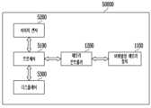
도 1을 참조하면, 메모리 시스템(Memory System; 1000)은 전원이 꺼져도 저장된 데이터가 소실되지 않는 비휘발성 메모리 장치(Nonvolatile Memory Device; 1100)와 데이터를 일시 저장하기 위한 버퍼 메모리 장치(Buffer Memory Device; 1300), 그리고 호스트(Host; 2000)의 제어에 따라 비휘발성 메모리 장치(1100) 및 버퍼 메모리 장치(1300)를 제어하는 메모리 컨트롤러(Memory Controller; 1200)를 포함할 수 있다.Referring to FIG. 1 , a
호스트(2000)는 USB (Universal Serial Bus), SATA (Serial AT Attachment), SAS (Serial Attached SCSI), HSIC (High Speed Interchip), SCSI (Small Computer System Interface), PCI (Peripheral Component Interconnection), PCIe (PCI express), NVMe (NonVolatile Memory express), UFS (Universal Flash Storage), SD (Secure Digital), MMC (MultiMedia Card), eMMC (embedded MMC), DIMM (Dual In-line Memory Module), RDIMM (Registered DIMM), LRDIMM (Load Reduced DIMM) 등과 같은 다양한 통신 방식들 중 적어도 하나를 이용하여 메모리 시스템(1000)과 통신할 수 있다.The
메모리 컨트롤러(1200)는 메모리 시스템(1000)의 동작을 전반적으로 제어하며, 호스트(2000)와 비휘발성 메모리 장치(1100) 사이의 데이터 교환을 제어할 수 있다. 예를 들면, 메모리 컨트롤러(1200)는 호스트(2000)의 요청에 따라 비휘발성 메모리 장치(1100)를 제어하여 데이터를 프로그램(program)하거나 리드(read)할 수 있다. 또한, 메모리 컨트롤러(1200)는 비휘발성 메모리 장치(1100)에 포함된 메인 메모리 블록들 및 서브 메모리 블록들의 정보를 저장하고, 프로그램 동작을 위해 로딩된 데이터 량에 따라 메인 메모리 블록 또는 서브 메모리 블록에 프로그램 동작이 수행되도록 비휘발성 메모리 장치(1100)를 선택할 수 있다. 실시예에 따라, 비휘발성 메모리 장치(1100)는 플래쉬 메모리(Flash Memory)를 포함할 수 있다.The
메모리 컨트롤러(1200)는 호스트(2000)와 버퍼 메모리 장치(1300) 사이의 데이터 교환을 제어하거나 또는 비휘발성 메모리 장치(1100)의 제어를 위한 시스템 데이터를 일시적으로 버퍼 메모리 장치(1300)에 저장할 수 있다. 버퍼 메모리 장치(1300)는 메모리 컨트롤러(1200)의 동작 메모리, 캐시 메모리 또는 버퍼 메모리로 사용될 수 있다. 버퍼 메모리 장치(1300)는 메모리 컨트롤러(1200)가 실행하는 코드들 및 커맨드들을 저장할 수 있다. 또한 버퍼 메모리 장치(1300)는 메모리 컨트롤러(1200)에 의해 처리되는 데이터를 저장할 수 있다.The
메모리 컨트롤러(1200)는 호스트(2000)로부터 입력된 데이터를 버퍼 메모리 장치(1300)에 일시 저장하고, 이후 버퍼 메모리 장치(1300)에 일시 저장된 데이터를 비휘발성 메모리 장치(1100)로 전송하여 저장할 수 있다. 또한 메모리 컨트롤러(1200)는 호스트(2000)로부터 데이터와 논리 어드레스(logical address)를 입력 받고, 논리 어드레스를 비휘발성 메모리 장치(1100) 내에 데이터가 실제 저장될 영역을 가리키는 물리 어드레스(physical address)로 변환할 수 있다. 또한 메모리 컨트롤러(1200)은 논리 어드레스와 물리 어드레스 간의 맵핑(mapping) 관계를 구성하는 논리-물리 어드레스 맵핑 테이블(logical-physical address mapping table)을 버퍼 메모리 장치(1300)에 저장할 수 있다.The
실시예에 따라, 버퍼 메모리 장치(1300)는 DDR SDRAM(Double Data Rate Synchronous Dynamic Random Access Memory), DDR4 SDRAM, LPDDR4(Low Power Double Data Rate4) SDRAM, GDDR(Graphics Double Data Rate) SDRAM, LPDDR(Low Power DDR) 또는 RDRAM(Rambus Dynamic Random Access Memory)을 포함할 수 있다.According to embodiments, the
실시예에 따라 메모리 시스템(1000)은 버퍼 메모리 장치(1300)를 포함하지 않을 수 있다.According to embodiments, the
도 2는 도 1의 비휘발성 메모리 장치를 설명하기 위한 도면이다.FIG. 2 is a diagram for explaining the nonvolatile memory device of FIG. 1 .
도 2를 참조하면, 비휘발성 메모리 장치(1100)는 데이터가 저장되는 메모리 셀 어레이(100)를 포함할 수 있다. 비휘발성 메모리 장치(1100)는 메모리 셀 어레이(100)에 데이터를 저장하기 위한 프로그램 동작(program operation), 저장된 데이터를 출력하기 위한 리드 동작(read operation) 및 저장된 데이터를 소거하기 위한 소거 동작(erase operation)을 수행하도록 구성된 주변 회로들(200)을 포함할 수 있다. 비휘발성 메모리 장치(1100)는 메모리 컨트롤러(도 1의 1200)의 제어에 따라 주변 회로들(200)을 제어하는 제어 로직(300)을 포함할 수 있다.Referring to FIG. 2 , a
메모리 셀 어레이(100)는 하나 이상의 메모리 플래인(Memory Plane; 101a, 101b)을 포함할 수 있다. 예시로서 메모리 셀 어레이(100)는 메모리 플래인들(101a, 101b)을 포함할 수 있다. 메모리 플래인들(101a, 101b) 각각은 동일한 형태로 구성될 수 있고 통칭하여 메모리 플래인(Memory Plane)이라고 부를 수 있다. 메모리 플래인(Memory Plane; 101a, 101b)에 포함된 다수의 메모리 블록들(110)은 포켓 P웰(pocket p-well)을 공유하여 형성될 수 있다.The
메모리 플래인들(101a, 101b) 각각은 다수의 메모리 블록들(BLK1~BLKm; 110 (m은 양의 정수))을 포함할 수 있다. 메모리 플래인(101a)에 포함된 각각의 메모리 블록들(BLK1~BLKm; 110)에는 제a 로컬 라인들(local lines; LLa)과 제a 비트 라인들(BL1a~BLna; n은 양의 정수)이 연결될 수 있다. 또한 메모리 플래인(101b)에 포함된 각각의 메모리 블록들(BLK1~BLKm; 110)에는 제b 로컬 라인들(local lines; LLb)과 제b 비트 라인들(BL1b~BLnb; n은 양의 정수)이 연결될 수 있다.Each of the
예를 들면, 제a 로컬 라인들(LLa) 및 제b 로컬 라인들(LLb) 각각은 제1 셀렉트 라인(first select line), 제2 셀렉트 라인(second select line), 상기 제1 및 제2 셀렉트 라인들 사이에 배열된 다수의 워드 라인들(word lines)을 포함할 수 있다. 또한, 제a 로컬 라인들(LLa) 및 제b 로컬 라인들(LLb) 각각은 제1 셀렉트 라인과 워드 라인들 사이, 제2 셀렉트 라인과 워드 라인들 사이에 배열된 더미 라인들을 포함할 수 있다. 여기서, 제1 셀렉트 라인은 소스 셀렉트 라인일 수 있고, 제2 셀렉트 라인은 드레인 셀렉트 라인일 수 있다. 예를 들면, 제a 로컬 라인들(LLa) 및 제b 로컬 라인들(LLb) 각각은 워드 라인들, 드레인 및 소스 셀렉트 라인들 및 소스 라인들(source lines)을 포함할 수 있다. 예를 들면, 제a 로컬 라인들(LLa) 및 제b 로컬 라인들(LLb) 각각은 더미 라인들(dummy lines)을 더 포함할 수 있다. 예를 들면, 제a 로컬 라인들(LLa) 및 제b 로컬 라인들(LLb) 각각은 파이프 라인들(pipe lines)을 더 포함할 수 있다.For example, each of the a th local lines LLa and the b th local lines LLb includes a first select line, a second select line, and the first and second select lines. It may include multiple word lines arranged between the lines. Also, each of the a-th local lines LLa and the b-th local lines LLb may include dummy lines arranged between the first select line and word lines and between the second select line and word lines. . Here, the first select line may be a source select line, and the second select line may be a drain select line. For example, each of the ath local lines LLa and the bth local lines LLb may include word lines, drain and source select lines, and source lines. For example, each of the ath local lines LLa and the bth local lines LLb may further include dummy lines. For example, each of the ath local lines LLa and the bth local lines LLb may further include pipe lines.
제a 로컬 라인들(LLa)은 메모리 플래인(101a)에 포함된 메모리 블록들(BLK1~BLKm; 110)에 각각 연결될 수 있으며, 제a 비트 라인들(BL1a~BLna)은 메모리 플래인(101a)에 포함된 메모리 블록들(BLK1~BLKm; 110)에 공통으로 연결될 수 있다. 또한 제b 로컬 라인들(LLb)은 메모리 플래인(101b)에 포함된 메모리 블록들(BLK1~BLKm; 110)에 각각 연결될 수 있으며, 제b 비트 라인들(BL1b~BLnb)은 메모리 플래인(101b)에 포함된 메모리 블록들(BLK1~BLKm; 110)에 공통으로 연결될 수 있다. 메모리 블록들(BLK1~BLKm; 110)은 2차원 또는 3차원 구조로 구현될 수 있다. 예를 들면, 2차원 구조의 메모리 블록들(110)에서 메모리 셀들은 기판에 평행한 방향으로 배열될 수 있다. 예를 들면, 3차원 구조의 메모리 블록들(110)에서 메모리 셀들은 기판에 수직 방향으로 적층될 수 있다.The a-th local lines LLa may be connected to memory blocks BLK1 to
주변 회로들(200)은 제어 로직(300)의 제어에 따라 선택된 메모리 블록(110)의 프로그램, 리드 및 소거 동작을 수행하도록 구성될 수 있다. 예를 들면, 주변 회로들(200)은 제어 로직(300)의 제어에 따라 제1 셀렉트 라인, 제2 셀렉트 라인 및 워드 라인들에 검증 전압 및 패스 전압들을 공급하고, 제1 셀렉트 라인, 제2 셀렉트 라인 및 워드 라인들을 선택적으로 디스차지할 수 있고, 워드 라인들 중 선택된 워드 라인에 연결된 메모리 셀들을 검증할 수 있다. 예를 들면, 주변 회로들(200)은 전압 생성 회로(voltage generating circuit; 210), 메모리 플래인(101a)에 연결된 로우 디코더(row decoder; 220a), 메모리 플래인(101b)에 연결된 로우 디코더(220b), 메모리 플래인(101a)에 연결된 페이지 버퍼 그룹(page buffer group; 230a), 메모리 플래인(101b)에 연결된 페이지 버퍼 그룹(page buffer group; 230b), 컬럼 디코더(column decoder; 240), 입출력 회로(input/output circuit; 250) 및 센싱 회로(sensing circuit; 260)를 포함할 수 있다.The
전압 생성 회로(210)는 동작 신호(OP_CMD)에 응답하여 프로그램, 리드 및 소거 동작들에 사용되는 다양한 동작 전압들(Vop)을 생성할 수 있다. 또한, 전압 생성 회로(210)는 동작 신호(OP_CMD)에 응답하여 로컬 라인들(LL)을 선택적으로 디스차지할 수 있다. 예를 들면, 전압 생성 회로(210)는 제어 로직(300)의 제어에 따라 프로그램 전압, 검증 전압, 패스 전압들, 턴온 전압, 리드 전압, 소거 전압 및 소스 라인 전압 등을 생성할 수 있다.The
첫번째 로우 디코더(row decoder; 220a)는 로우 어드레스(RADD)에 응답하여 동작 전압들(Vop)을 선택된 메모리 플래인(101a)에 포함된 메모리 블록(110)에 연결된 제a 로컬 라인들(LLa)에 전달할 수 있다. 또한 두번째 로우 디코더(row decoder; 220b)는 로우 어드레스(RADD)에 응답하여 동작 전압들(Vop)을 선택된 메모리 플래인(101b)에 포함된 메모리 블록(110)에 연결된 제b 로컬 라인들(LLb)에 전달할 수 있다.A
첫번째 페이지 버퍼 그룹(page buffer group; 230a)은 제a 비트 라인들(BL1a~BLna)에 연결된 다수의 페이지 버퍼들(PB1~PBn; 231)을 포함할 수 있고, 두번째 페이지 버퍼 그룹(page buffer group; 230b)은 제b 비트 라인들(BL1b~BLnb)에 연결된 다수의 페이지 버퍼들(PB1~PBn; 231)을 포함할 수 있다. 페이지 버퍼들(PB1~PBn; 231)은 페이지 버퍼 제어 신호들(PBSIGNALS)에 응답하여 동작할 수 있다. 예를 들면, 페이지 버퍼 그룹(page buffer group; 230a)에 포함된 페이지 버퍼들(PB1~PBn; 231)은 제a 비트 라인들(BL1a~BLna)을 통해 수신된 데이터를 임시로 저장하거나, 리드 또는 검증 동작 시, 제a 비트 라인들(BL1a~BLna)의 전압 또는 전류를 센싱(sensing)할 수 있다.The first
컬럼 디코더(240)는 컬럼 어드레스(CADD)에 응답하여 입출력 회로(250)와 페이지 버퍼 그룹(page buffer group; 230a, 230b) 사이에서 데이터를 전달할 수 있다. 예를 들면, 컬럼 디코더(240)는 제a 데이터 라인들(DLa)을 통해 페이지 버퍼 그룹(page buffer group; 230a)에 포함된 페이지 버퍼들(231)과 데이터를 주고 받거나, 제b 데이터 라인들(DLb)을 통해 페이지 버퍼 그룹(page buffer group; 230b)에 포함된 페이지 버퍼들(231)과 데이터를 주고 받을 수 있다. 또한 컬럼 디코더(240)는 컬럼 라인들(CL)을 통해 입출력 회로(250)와 데이터를 주고받을 수 있다.The
입출력 회로(250)는 메모리 컨트롤러(도 1의 1200)로부터 전달 받은 커맨드(CMD) 및 어드레스(ADD)를 제어 로직(300)에 전달하거나, 데이터(DATA)를 컬럼 디코더(240)와 주고받을 수 있다. 이때 어드레스(ADD)는 로우 어드레스(RADD) 및 컬럼 어드레스(CADD)를 포함할 수 있다.The input/
센싱 회로(260)는 리드 동작(read operation) 또는 검증 동작(verify operation)시, 허용 비트(VRY_BIT<#>)에 응답하여 기준 전류를 생성하고, 페이지 버퍼 그룹(page buffer group; 230a)으로부터 수신된 제a 센싱 전압(VPBa) 또는 페이지 버퍼 그룹(page buffer group; 230b)으로부터 수신된 제b 센싱 전압(VPBb)과 기준 전류에 의해 생성된 기준 전압을 비교하여 패스 신호(PASS) 또는 페일 신호(FAIL)를 출력할 수 있다.During a read operation or a verify operation, the
제어 로직(300)은 커맨드(CMD) 및 어드레스(ADD)에 응답하여 동작 신호(OP_CMD), 로우 어드레스(RADD), 페이지 버퍼 제어 신호들(PBSIGNALS) 및 허용 비트(VRY_BIT<#>)를 출력하여 주변 회로들(200)을 제어할 수 있다. 또한, 제어 로직(300)은 패스 또는 페일 신호(PASS 또는 FAIL)에 응답하여 검증 동작이 패스 또는 페일 되었는지를 판단할 수 있다.
비휘발성 메모리 장치(1100)의 동작에 있어 각각의 메모리 블록(110)은 소거 동작의 단위 일 수 있다. 다시 말해 하나의 메모리 블록(110)에 포함된 다수의 메모리 셀들은 서로 동시에 소거되며, 선별적으로 소거되지 못할 수 있다.In the operation of the
입출력 회로(250)는 외부로부터 데이터 입출력 핀들(DQ<7:0>)을 통해 전달 받은 데이터를 컬럼 라인들(CL)을 통해 컬럼 디코더(240)로 전송 할 수 있다. 이때 데이터 입출력 핀들(DQ<7:0>)을 통해 입력 되는 데이터는 칩 인에이블 신호(CE)가 활성화된 동안 리드 인에이블 신호(RE)에 동기하여 입력 될 수 있다. 다른 예시로서 데이터 입출력 핀들(DQ<7:0>)을 통해 입력 되는 데이터는 칩 인에이블 신호(CE)가 활성화된 동안 라이트 인에이블 신호(WE)에 동기하여 입력 될 수 있다. 또한 입출력 회로(250)는 컬럼 디코더(240)로부터 출력되어 컬럼 라인들(CL)을 통해 전송된 데이터를 데이터 입출력 핀들(DQ<7:0>)을 통해 외부 장치로 출력할 수 있다. 이때 출력 되는 데이터는 칩 인에이블 신호(CE)가 활성화된 동안 데이터 스트로브 클럭 신호(DQS)에 동기하여 출력 될 수 있다. 다른 예시로서 출력 되는 데이터는 칩 인에이블 신호(CE)가 활성화된 동안 리드 인에이블 신호(RE)에 동기하여 출력 될 수 있다.The input/
입출력 회로(250)는 커맨드 래치 인에이블 신호(CLE)가 활성화된 구간에서 외부 장치로부터 커맨드를 입력 받아 제어 회로(300)에 전달할 수 있고, 어드레스 래치 인에이블 신호(ALE)가 활성화된 구간에서 외부 장치로부터 어드레스를 입력 받아 제어 회로(300)에 전달할 수 있다.The input/
도 3은 도 2의 메모리 블록을 설명하기 위한 도면이다.FIG. 3 is a diagram for explaining the memory block of FIG. 2 .
도 3을 참조하면, 메모리 블록(110)은 제1 셀렉트 라인과 제2 셀렉트 라인 사이에 서로 평행하게 배열된 다수의 워드 라인들이 연결될 수 있다. 여기서, 제1 셀렉트 라인은 소스 셀렉트 라인(SSL)일 수 있고, 제2 셀렉트 라인은 드레인 셀렉트 라인(DSL)일 수 있다. 보다 구체적으로 설명하면, 메모리 블록(110)은 비트 라인들(BL1~BLn)과 소스 라인(SL) 사이에 연결된 다수의 스트링들(strings; ST)을 포함할 수 있다. 비트 라인들(BL1~BLn)은 스트링들(ST)에 각각 연결될 수 있고, 소스 라인(SL)은 스트링들(ST)에 공통으로 연결될 수 있다. 스트링들(ST)은 서로 동일하게 구성될 수 있으므로, 제1 비트 라인(BL1)에 연결된 스트링(ST)을 예를 들어 구체적으로 설명하도록 한다.Referring to FIG. 3 , in the
스트링(ST)은 소스 라인(SL)과 제1 비트 라인(BL1) 사이에서 서로 직렬로 연결된 소스 셀렉트 트랜지스터(SST), 다수의 메모리 셀들(F1~F16) 및 드레인 셀렉트 트랜지스터(DST)를 포함할 수 있다. 하나의 스트링(ST)에는 소스 셀렉트 트랜지스터(SST)와 드레인 셀렉트 트랜지스터(DST)가 적어도 하나 이상씩 포함될 수 있으며, 메모리 셀들(F1~F16) 또한 도면에 도시된 개수보다 더 많이 포함될 수 있다.The string ST may include a source select transistor SST, a plurality of memory cells F1 to F16, and a drain select transistor DST connected in series between the source line SL and the first bit line BL1. can One string ST may include at least one source select transistor SST and at least one drain select transistor DST, and memory cells F1 to F16 may also include more than the number shown in the drawing.
소스 셀렉트 트랜지스터(SST)의 소스(source)는 소스 라인(SL)에 연결될 수 있고, 드레인 셀렉트 트랜지스터(DST)의 드레인(drain)은 제1 비트 라인(BL1)에 연결될 수 있다. 메모리 셀들(F1~F16)은 소스 셀렉트 트랜지스터(SST)와 드레인 셀렉트 트랜지스터(DST) 사이에서 직렬로 연결될 수 있다. 서로 다른 스트링들(ST)에 포함된 소스 셀렉트 트랜지스터들(SST)의 게이트들은 소스 셀렉트 라인(SSL)에 연결될 수 있고, 드레인 셀렉트 트랜지스터들(DST)의 게이트들은 드레인 셀렉트 라인(DSL)에 연결될 수 있고, 메모리 셀들(F1~F16)의 게이트들은 다수의 워드 라인들(WL1~WL16)에 연결될 수 있다. 서로 다른 스트링들(ST)에 포함된 메모리 셀들 중에서 동일한 워드 라인에 연결된 메모리 셀들의 그룹을 물리 페이지(physical page; PPG)라 할 수 있다. 따라서, 메모리 블록(110)에는 워드 라인들(WL1~WL16)의 개수만큼의 물리 페이지들(PPG)이 포함될 수 있다.A source of the source select transistor SST may be connected to the source line SL, and a drain of the drain select transistor DST may be connected to the first bit line BL1. The memory cells F1 to F16 may be connected in series between the source select transistor SST and the drain select transistor DST. Gates of the source select transistors SST included in the different strings ST may be connected to the source select line SSL, and gates of the drain select transistors DST may be connected to the drain select line DSL. gates of the memory cells F1 to F16 may be connected to a plurality of word lines WL1 to WL16. A group of memory cells connected to the same word line among memory cells included in different strings ST may be referred to as a physical page (PPG). Accordingly, the
하나의 메모리 셀은 1비트 데이터를 저장할 수 있다. 이를 통상적으로 싱글 레벨 셀(single level cell; SLC)라고 부른다. 이 경우 하나의 물리 페이지(PPG)는 하나의 논리 페이지(logical page; LPG) 데이터를 저장할 수 있다. 하나의 논리 페이지(LPG) 데이터는 하나의 물리 페이지(PPG)에 포함된 셀 개수 만큼의 데이터 비트들을 포함할 수 있다. 또한 하나의 메모리 셀(MC)은 2비트의 데이터를 저장할 수 있다. 이를 통상적으로 멀티 레벨 셀(multi-level cell; MLC)이라고 부른다. 이 경우 하나의 물리 페이지(PPG)는 2개의 논리 페이지(logical page; LPG) 데이터를 저장할 수 있다. 다른 예시로서 하나의 메모리 셀(MC)은 3비트의 데이터를 저장할 수 있다. 이를 통상적으로 트리플 레벨 셀(triple-level cell; TLC)이라고 부른다. 이 경우 하나의 물리 페이지(PPG)는 3개의 논리 페이지(logical page; LPG) 데이터를 저장할 수 있다. 또한 하나의 메모리 셀(MC)은 4비트의 데이터를 저장할 수 있다. 이를 통상적으로 쿼드러플 레벨 셀(quadruple-level cell; QLC)이라고 부른다. 이 경우 하나의 물리 페이지(PPG)는 4개의 논리 페이지(logical page; LPG) 데이터를 저장할 수 있다.One memory cell can store 1-bit data. This is commonly referred to as a single level cell (SLC). In this case, one physical page (PPG) can store one logical page (LPG) data. One logical page (LPG) data may include as many data bits as the number of cells included in one physical page (PPG). Also, one memory cell MC may store 2-bit data. This is commonly referred to as a multi-level cell (MLC). In this case, one physical page (PPG) can store two logical page (LPG) data. As another example, one memory cell MC may store 3-bit data. This is commonly referred to as a triple-level cell (TLC). In this case, one physical page (PPG) can store three logical page (LPG) data. Also, one memory cell MC may store 4-bit data. This is commonly referred to as a quadruple-level cell (QLC). In this case, one physical page (PPG) can store four logical page (LPG) data.
메모리 셀이 2비트의 데이터를 저장할 때 하나의 물리 페이지(PPG)는 2개의 페이지들(PG)을 포함할 수 있다. 이때 하나의 페이지(PG)는 하나의 논리 페이지(LPG) 데이터를 저장할 수 있다. 하나의 메모리 셀은 데이터에 따라 다수의 문턱 전압들(threshold voltage) 중 어느 하나를 가질 수 있고, 하나의 물리 페이지(PPG)에 포함된 다수의 페이지들(PG)은 문턱 전압(threshold voltage)의 차이로 표현될 수 있다.When a memory cell stores 2-bit data, one physical page PPG may include two pages PG. In this case, one page (PG) may store one logical page (LPG) data. One memory cell may have one of a plurality of threshold voltages according to data, and a plurality of pages PG included in one physical page PPG may have a threshold voltage difference can be expressed.
하나의 메모리 블록(110)에 포함된 다수의 메모리 셀들은 싱글 레벨 셀들(SLC)로 구동될 수 있다. 다시 말해 하나의 메모리 블록(110)에 포함된 다수의 메모리 셀들은 싱글 레벨 셀들(SLC)로 프로그램 되고 리드 될 수 있다. 이러한 메모리 블록(110)을 싱글 레벨 셀 블록(SLC Block)이라고 명명할 수 있다. 또한 하나의 메모리 블록(110)에 포함된 다수의 메모리 셀들은 멀티 레벨 셀들(MLC)로 구동될 수 있다. 다시 말해 하나의 메모리 블록(110)에 포함된 다수의 메모리 셀들은 멀티 레벨 셀들(MLC)로 프로그램 되고 리드 될 수 있다. 이러한 메모리 블록(110)을 멀티 레벨 셀 블록(MLC Block)이라고 명명할 수 있다.A plurality of memory cells included in one
하나의 메모리 블록(110)에 포함된 다수의 메모리 셀들은 트리플 레벨 셀들(TLC)로 구동될 수 있다. 다시 말해 하나의 메모리 블록(110)에 포함된 다수의 메모리 셀들은 트리플 레벨 셀들(TLC)로 프로그램 되고 리드 될 수 있다. 이러한 메모리 블록(110)을 트리플 레벨 셀 블록(TLC Block)이라고 명명할 수 있다. 또한 하나의 메모리 블록(110)에 포함된 다수의 메모리 셀들은 쿼드러플 레벨 셀들(QLC)로 구동될 수 있다. 다시 말해 하나의 메모리 블록(110)에 포함된 다수의 메모리 셀들은 쿼드러플 레벨 셀들(QLC)로 프로그램 되고 리드 될 수 있다. 이러한 메모리 블록(110)을 쿼드러플 레벨 셀 블록(QLC Block)이라고 명명할 수 있다.A plurality of memory cells included in one
비휘발성 메모리 장치(1100)은 하나 이상의 싱글 레벨 셀 블록(SLC Block), 하나 이상의 멀티 레벨 셀 블록(MLC Block), 하나 이상의 트리플 레벨 셀 블록(TLC Block) 및 하나 이상의 쿼드러플 레벨 셀 블록(QLC Block)을 포함할 수 있다.The
도 4는 도 1의 메모리 컨트롤러를 설명하기 위한 도면이다.FIG. 4 is a diagram for explaining the memory controller of FIG. 1 .
도 4를 참고하면, 메모리 컨트롤러(1200)는 프로세서부(Processor; 710), 메모리 버퍼부(Memory Buffer; 720), 에러 정정부(ECC; 730), 호스트 인터페이스(Host Interface; 740), 버퍼 제어부(Buffer Control Circuit; 750), 플래쉬 인터페이스(Flash Interface; 760), 데이터 랜더마이저(Data Randomizer; 770), 버퍼 메모리 인터페이스(Buffer Memory Interface; 780) 및 버스(Bus; 790)를 포함할 수 있다.Referring to FIG. 4 , the
버스(790)는 메모리 컨트롤러(1200)의 구성 요소들 사이에 채널(channel)을 제공하도록 구성될 수 있다.The
메모리 버퍼부(720)는 프로세서부(710)의 동작 메모리, 캐시 메모리 또는 버퍼 메모리로 사용될 수 있다. 메모리 버퍼부(720)는 프로세서부(710)가 실행하는 코드들 및 커맨드들을 저장할 수 있다. 메모리 버퍼부(720)는 프로세서부(710)에 의해 처리되는 데이터를 저장할 수 있다. 메모리 버퍼부(720)는 SRAM(Static RAM), 또는 DRAM(Dynamic RAM)을 포함할 수 있다.The
에러 정정부(730)는 에러 정정을 수행할 수 있다. 에러 정정부(730)는 플래쉬 인터페이스(760)를 통해 비휘발성 메모리 장치(1100)에 기입될 데이터에 기반하여 에러 정정 인코딩(ECC encoding)을 수행할 수 있다. 에러 정정 인코딩 된 데이터는 플래쉬 인터페이스(760)를 통해 비휘발성 메모리 장치(1100)로 전달될 수 있다. 에러 정정부(730)는 비휘발성 메모리 장치(1100)로부터 플래쉬 인터페이스(760)를 통해 수신되는 데이터에 대해 에러 정정 디코딩(ECC decoding)을 수행할 수 있다. 예시적으로, 에러 정정부(730)는 플래쉬 인터페이스(760)의 구성 요소로서 플래쉬 인터페이스(760)에 포함될 수 있다.The
호스트 인터페이스(740)는 프로세서부(710)의 제어에 따라, 외부의 호스트(2000)와 통신하도록 구성된다. 호스트 인터페이스(740)는 USB (Universal Serial Bus), SATA (Serial AT Attachment), SAS (Serial Attached SCSI), HSIC (High Speed Interchip), SCSI (Small Computer System Interface), PCI (Peripheral Component Interconnection), PCIe (PCI express), NVMe (NonVolatile Memory express), UFS (Universal Flash Storage), SD (Secure Digital), MMC (MultiMedia Card), eMMC (embedded MMC), DIMM (Dual In-line Memory Module), RDIMM (Registered DIMM), LRDIMM (Load Reduced DIMM) 등과 같은 다양한 통신 방식들 중 적어도 하나를 이용하여 통신하도록 구성될 수 있다.The
버퍼 제어부(750)는 프로세서부(710)의 제어에 따라, 메모리 버퍼부(720)를 제어하도록 구성될 수 있다.The
플래쉬 인터페이스(760)는 프로세서부(710)의 제어에 따라, 비휘발성 메모리 장치(1100)와 통신하도록 구성된다. 플래쉬 인터페이스(760)는 채널을 통해 커맨드, 어드레스 및 데이터를 비휘발성 메모리 장치(1100)와 통신할 수 있다.The
예시적으로, 메모리 컨트롤러(1200)는 메모리 버퍼부(720) 및 버퍼 제어부(750)를 포함하지 않을 수 있다.For example, the
데이터 랜더마이저(Data Randomizer; 770)는 데이터를 랜덤화(randomizing) 하거나 랜덤화 된 데이터를 디랜덤화(de-randomizing) 할 수 있다. 데이터 랜더마이저(770)는 플래쉬 인터페이스(760)를 통해 비휘발성 메모리 장치(1100)에 기입될 데이터에 대해 데이터 랜덤화 동작을 수행할 수 있다. 랜덤화 된 데이터는 플래쉬 인터페이스(760)를 통해 비휘발성 메모리 장치(1100)로 전달될 수 있다. 데이터 랜더마이저(770)는 비휘발성 메모리 장치(1100)로부터 플래쉬 인터페이스(760)를 통해 수신되는 데이터에 대해 데이터 디랜덤화 동작을 수행할 수 있다. 예시적으로, 데이터 랜더마이저(770)는 플래쉬 인터페이스(760)의 구성 요소로서 플래쉬 인터페이스(760)에 포함될 수 있다.The data randomizer 770 may randomize data or de-randomize randomized data. The data randomizer 770 may perform a data randomization operation on data to be written in the
예시적으로, 메모리 컨트롤러(1200)의 버스(790)는 제어 버스(control bus) 및 데이터 버스(data bus)로 구분될 수 있다. 데이터 버스는 메모리 컨트롤러(1200) 내에서 데이터를 전송하고, 제어 버스는 메모리 컨트롤러(1200) 내에서 커맨드, 어드레스와 같은 제어 정보를 전송하도록 구성될 수 있다. 데이터 버스와 제어 버스는 서로 분리되며, 상호간에 간섭하거나 영향을 주지 않을 수 있다. 데이터 버스는 호스트 인터페이스(740), 버퍼 제어부(750), 에러 정정부(730), 플래쉬 인터페이스(760) 및 버퍼 메모리 인터페이스(780)에 연결될 수 있다. 제어 버스는 호스트 인터페이스(740), 프로세서부(710), 버퍼 제어부(750), 플래쉬 인터페이스(760) 및 버퍼 메모리 인터페이스(780)에 연결될 수 있다. 실시예에 따라 메모리 컨트롤러(1200)는 버퍼 메모리 인터페이스(780)를 포함하지 않을 수 있다.For example, the
버퍼 메모리 인터페이스(780)는 프로세서부(710)의 제어에 따라 버퍼 메모리 장치(1300)와 통신하도록 구성될 수 있다. 버퍼 메모리 인터페이스(780)는 채널을 통해 커맨드, 어드레스 및 데이터를 버퍼 메모리 장치(1300)와 교신할 수 있다.The
프로세서부(710)는 메모리 컨트롤러(1200)의 제반 동작을 제어하고, 논리 연산을 수행할 수 있다. 프로세서부(710)는 호스트 인터페이스(740)를 통해 외부의 호스트(2000)와 통신하고, 플래쉬 인터페이스(760)를 통해 비휘발성 메모리 장치(1100)와 통신할 수 있다. 또한 프로세서부(710)는 버퍼 메모리 인터페이스(780)를 통해 버퍼 메모리 장치(1300)와 통신할 수 있다. 또한 프로세서부(710)는 버퍼 제어부(750)를 통해 메모리 버퍼부(720)를 제어할 수 있다. 프로세서부(710)는 메모리 버퍼부(720)를 동작 메모리, 캐시 메모리(cache memory) 또는 버퍼 메모리(buffer memory)로 사용하여 메모리 시스템(1000)의 동작을 제어할 수 있다.The
프로세서부(710)는 호스트(2000)로부터 입력된 다수의 커맨드들을 큐잉(queuing)할 수 있다. 이러한 동작을 멀티-큐(multi-queue)라고 부른다. 프로세서부(710)는 큐잉된 다수의 커맨드들을 순차적으로 비휘발성 메모리 장치(1100)에 전달할 수 있다.The
프로세서부(710)는 비휘발성 메모리 장치(1100)을 제어하기 위한 리드 커맨드/어드레스 시퀀스(Read Command/Address Sequence), 프로그램 커맨드/어드레스 시퀀스(Program Command/Address Sequence) 및 소거 커맨드/어드레스 시퀀스(Erase Command/Address Sequence)를 생성할 수 있다. 리드 커맨드/어드레스 시퀀스(Read Command/Address Sequence), 프로그램 커맨드/어드레스 시퀀스(Program Command/Address Sequence) 및 소거 커맨드/어드레스 시퀀스(Erase Command/Address Sequence)는 각각 하나 이상의 커맨드 유닛(Command Unit) 및 하나 이상의 어드레스(Address)를 포함할 수 있다. 메모리 컨트롤러(1200)는 커맨드 래치 인에이블 신호(Command Latch Enable, CLE)가 활성화 된 동안 라이트 인에이블 신호(Write Enable; WE)에 동기하여 비휘발성 메모리 장치(1100)에 커맨드 유닛(Command Unit)을 입력할 수 있다. 또한 메모리 컨트롤러(1200)는 어드레스 래치 인에이블 신호(Address Latch Enable, ALE)가 활성화 된 동안 라이트 인에이블 신호(Write Enable; WE)에 동기하여 동기하여 비휘발성 메모리 장치(1100)에 어드레스(Address)를 입력할 수 있다. 비휘발성 메모리 장치(1100)는 메모리 컨트롤러(1200)로부터 수신한 리드 커맨드/어드레스 시퀀스(Read Command/Address Sequence), 프로그램 커맨드/어드레스 시퀀스(Program Command/Address Sequence) 및 소거 커맨드/어드레스 시퀀스(Erase Command/Address Sequence)에 응답하여 리드 동작, 프로그램 동작 및 소거 동작을 수행할 수 있다.The
예시로서 메모리 시스템(1000)은 호스트(2000)로부터 리드 커맨드 및 논리 어드레스를 포함하는 리드 리퀘스트(Read Request)를 수신할 수 있고, 프로세서부(710)는 호스트(2000)로부터 수신한 리드 리퀘스트(Read Request)에 응답하여 리드 커맨드/어드레스 시퀀스(Read Command/Address Sequence)를 생성하여 비휘발성 메모리 장치(1100)에 제공할 수 있다.As an example, the
다른 예시로서 가비지 컬렉션 동작(Garbage Collection Operation)과 같은 메모리 시스템(1000) 내부적인 요청으로 발생하는 동작, 즉 하우스 키핑(House Keeping) 동작에 의해 리드 리퀘스트(Read Request)가 발생할 수 있고, 프로세서부(710)는 하우스 키핑(House Keeping) 동작에 의해 발생한 리드 리퀘스트(Read Request)에 응답하여 리드 커맨드/어드레스 시퀀스(Read Command/Address Sequence)를 생성하여 비휘발성 메모리 장치(1100)에 제공할 수 있다.As another example, a read request may be generated by an operation generated by an internal request of the
메모리 시스템(1000)은 호스트(2000)로부터 입력된 기입 커맨드 및 논리 어드레스를 포함하는 기입 리퀘스트(Write Request) 또는 하우스 키핑(House Keeping) 동작에 의해 발생한 프로그램 리퀘스트(Program Request)에 응답하여 프로그램 커맨드/어드레스 시퀀스(Program Command/Address Sequence)를 생성하여 비휘발성 메모리 장치(1100)에 제공할 수 있다.The
메모리 시스템(1000)은 호스트(2000)로부터 입력된 언맵 커맨드(Unmap Command) 및 논리 어드레스를 포함하는 언맵 리퀘스트(Unmap Request) 또는 하우스 키핑(House Keeping) 동작에 의해 발생한 소거 리퀘스트(Erase Request)에 응답하여 소거 커맨드/어드레스 시퀀스(Erase Command/Address Sequence)를 생성하여 비휘발성 메모리 장치(1100)에 제공할 수 있다.The
프로세서부(710)는 펌웨어부(Firmware Section; 711), 하드웨어부(Hardware Section; 712) 및 플래쉬 변환부(Flash Translation Section; 713)를 포함할 수 있다.The
펌웨어부(711)는 롬(Read Only Memory; ROM)을 포함할 수 있고, 롬(ROM)에는 펌웨어 코드(Firmware Code)가 저장될 수 있다. 펌웨어 코드는 제조사가 제조 과정에서 롬(ROM)에 저장하는 코드일 수 있다. 다른 예로서, 프로세서부(710)는 비휘발성 메모리 장치(1100)로부터 플래쉬 인터페이스(760)를 통해 펌웨어 코드들을 로드(load)할 수 있다. 또한 메모리 컨트롤러(1200)의 펌웨어부(711)는 파워 온 후 부팅 과정에서 펌웨어 코드(Firmware Code)를 실행할 수 있다.The
펌웨어 코드(Firmware Code)에는 메모리 시스템(1000)의 동작에 필요한 다양한 정보가 포함될 수 있다. 예시로서 펌웨어 코드(Firmware Code)는 메모리 시스템(1000)에 포함된 비휘발성 메모리 장치(1100)의 구성 정보, 예시로서 비휘발성 메모리 장치(1100)에 포함된 메모리 플래인(Memory Plane; 101a, 101b)의 수에 대한 정보를 포함할 수 있다. 또한 펌웨어 코드(Firmware Code)는 비휘발성 메모리 장치(1100)에 포함된 다수의 메모리 블록들(110)에 포함된 메모리 셀들의 셀당 비트 수(Number of Bits per Cell)에 대한 정보를 포함할 수 있다.The firmware code may include various pieces of information necessary for the operation of the
메모리 시스템(1000)은 호스트(2000)로부터 기입 커맨드(write command) 및 기입 데이터(write data), 그리고 논리 어드레스(logical address)를 수신할 수 있다. 플래쉬 변환부(Flash Translation Section; 713)는 기입 커맨드(write command)에 응답하여 기입 데이터(write data)를 저장할 비휘발성 메모리 장치(1100) 내 물리적 저장 공간, 다시 말해 메모리 블록(110) 또는 페이지(page)를 할당할 수 있다. 다시 말해 플래쉬 변환부(Flash Translation Section; 713)는 기입 커맨드(write command)에 응답하여 논리 어드레스(logical address)에 대응하는 물리 어드레스(physical address)를 맵핑할 수 있다. 이때 물리 어드레스(physical address)는 호스트(2000)로부터 수신한 기입 데이터(write data)를 저장할 비휘발성 메모리 장치(1100)의 물리적 저장 공간에 대응하는 어드레스 일 수 있다.The
하드웨어부(712)는 물리 어드레스(physical address)에 대응하는 비휘발성 메모리 장치(1100) 내 저장 영역에 데이터를 프로그램 하는 동작을 제어할 수 있다.The
메모리 시스템(1000)은 호스트(2000)로부터 리드 커맨드(read command) 및 논리 어드레스(logical address)를 수신할 수 있다. 플래쉬 변환부(Flash Translation Section; 713)는 리드 커맨드(read command)에 응답하여 비휘발성 메모리 장치(1100)에 저장된 상기 논리 어드레스에 대응하는 논리-물리 어드레스 맵핑 정보(logical-to-physical address mapping information)를 리드하여 메모리 버퍼부(720)에 로드할 수 있다.The
하드웨어부(712)는 메모리 버퍼부(720)에 로드된 논리-물리 어드레스 맵핑 정보(logical-to-physical address mapping information)로부터 논리 어드레스(logical address)에 대응하는 물리 어드레스(physical address)를 확인하고, 물리 어드레스(physical address)에 대응하는 비휘발성 메모리 장치(1100) 내 저장 영역에 저장된 데이터를 리드 하여 호스트(2000)로 출력할 수 있다.The
프로세서부(710)는 상술한 비휘발성 메모리 장치(1100)에 포함된 메모리 플래인(Memory Plane; 101a, 101b)의 수 또는 메모리 셀들의 셀당 비트 수(Number of Bits per Cell)에 대한 정보에 기초하여 리드 커맨드/어드레스 시퀀스(Read Command/Address Sequence), 프로그램 커맨드/어드레스 시퀀스(Program Command/Address Sequence) 및 소거 커맨드/어드레스 시퀀스(Erase Command/Address Sequence)를 생성하여 비휘발성 메모리 장치(1100)에 제공할 수 있다.The
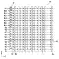
도 5는 리드 커맨드/어드레스 시퀀스들을 설명하기 위한 도면이다.5 is a diagram for explaining read command/address sequences.
도 5를 참조하면, 프로세서부(710)는 비휘발성 메모리 장치(1100)에 저장된 데이터를 리드 하기 위하여 다수의 리드 커맨드/어드레스 시퀀스들(Read Command/Address Sequence)을 생성하고, 생성된 리드 커맨드/어드레스 시퀀스들(Read Command/Address Sequence)을 비휘발성 메모리 장치(1100)에 제공할 수 있다.Referring to FIG. 5 , the
예시로서 프로세서부(710)는 비휘발성 메모리 장치(1100)에 포함된 하나의 메모리 플래인(101a, 101b)에 포함된 싱글 레벨 셀들(SLC)을 포함한 물리 페이지(PPG)에 저장된 논리 페이지 데이터를 리드 하기 위하여 제1 리드 커맨드/어드레스 시퀀스(RD_CMDADDSeq1)을 생성할 수 있다. 제1 리드 커맨드/어드레스 시퀀스(RD_CMDADDSeq1)는 싱글 레벨 셀 블록(SLC Block) 또는 싱글 레벨 셀들(SLC)을 포함한 페이지(PG)임을 가리키는 제1 SLC 커맨드 유닛(CMDUnit-1(SLC))을 포함할 수 있다.As an example, the
또한 제1 리드 커맨드/어드레스 시퀀스(RD_CMDADDSeq1)는 하나의 물리 페이지(PPG)의 첫번째 페이지에 저장된 하나의 논리 페이지(logical page; LPG) 데이터를 리드함을 가리키는 제2 1P 커맨드 유닛(CMDUnit-2(1P))을 포함할 수 있다. 이때 싱글 레벨 셀들(SLC)을 포함한 물리 페이지(PPG)의 경우 하나의 물리 페이지(PPG)에 하나의 논리 페이지(logical page; LPG) 데이터가 저장되기 때문에 제1 리드 커맨드/어드레스 시퀀스(RD_CMDADDSeq1)는 제2 1P 커맨드 유닛(CMDUnit-2(1P))을 포함하지 않고 제2 1P 커맨드 유닛(CMDUnit-2(1P))는 스킵(skip) 될 수도 있다.In addition, the first read command/address sequence RD_CMDADDSeq1 indicates that one logical page (LPG) data stored in the first page of one physical page PPG is read, and the second 1P command unit CMDUnit-2 ( 1P)). At this time, in the case of a physical page (PPG) including single-level cells (SLC), since one logical page (LPG) data is stored in one physical page (PPG), the first read command/address sequence (RD_CMDADDSeq1) is The second 1P command unit CMDUnit-2(1P) may be skipped without including the second 1P command unit CMDUnit-2(1P).
제1 리드 커맨드/어드레스 시퀀스(RD_CMDADDSeq1)는 요청된 동작이 리드 동작임을 가리키는 제3 리드 커맨드 유닛(CMDUnit-3(READ))을 포함할 수 있다.The first read command/address sequence RD_CMDADDSeq1 may include a third read command unit CMDUnit-3 (READ) indicating that the requested operation is a read operation.
메모리 컨트롤러(1200)는 커맨드 래치 인에이블 신호(CLE)가 활성화 된 동안 라이트 인에이블 신호(Write Enable; WE)에 동기하여 제1 SLC 커맨드 유닛(CMDUnit-1(SLC), 제2 1P 커맨드 유닛(CMDUnit-2(1P)) 및 제3 리드 커맨드 유닛(CMDUnit-3(READ))을 비휘발성 메모리 장치(1100)에 제공할 수 있다.The
비휘발성 메모리 장치(1100)에 제1 SLC 커맨드 유닛(CMDUnit-1(SLC), 제2 1P 커맨드 유닛(CMDUnit-2(1P)) 및 제3 리드 커맨드 유닛(CMDUnit-3(READ)) 각각이 제공되는 순서는 가변적일 수 있다.A first SLC command unit (CMDUnit-1 (SLC)), a second 1P command unit (CMDUnit-2 (1P)), and a third read command unit (CMDUnit-3 (READ)) are respectively included in the
제1 리드 커맨드/어드레스 시퀀스(RD_CMDADDSeq1)는 리드 동작이 수행될 메모리 셀들에 대응하는 로우 어드레스(RADD) 및 컬럼 어드레스(CADD)를 포함할 수 있다. 메모리 컨트롤러(1200)는 어드레스 래치 인에이블 신호(ALE)가 활성화 된 동안 라이트 인에이블 신호(Write Enable; WE)에 동기하여 로우 어드레스(RADD) 및 컬럼 어드레스(CADD)를 비휘발성 메모리 장치(1100)에 제공할 수 있다. 예시로서 메모리 컨트롤러(1200)는 비휘발성 메모리 장치(1100)에 로우 어드레스(RADD)를 제공한 후 컬럼 어드레스(CADD)를 제공할 수 있고, 반대로 컬럼 어드레스(CADD)를 제공한 후 로우 어드레스(RADD)를 제공할 수도 있다.The first read command/address sequence RD_CMDADDSeq1 may include row addresses RADD and column addresses CADD corresponding to memory cells on which a read operation is to be performed. The
제1 리드 커맨드/어드레스 시퀀스(RD_CMDADDSeq1)는 하나의 메모리 플래인(101a, 101b)에 대해 리드 동작을 요청함을 가리키는 제4 싱글 커맨드 유닛(CMDUnit-4(Single))을 포함할 수 있다. 메모리 컨트롤러(1200)는 커맨드 래치 인에이블 신호(CLE)가 활성화 된 동안 라이트 인에이블 신호(Write Enable; WE)에 동기하여 제4 싱글 커맨드 유닛(CMDUnit-4(Single))을 비휘발성 메모리 장치(1100)에 제공할 수 있다.The first read command/address sequence RD_CMDADDSeq1 may include a fourth single command unit CMDUnit-4 (Single) indicating that a read operation is requested for one
비휘발성 메모리 장치(1100)는 제4 커맨드 유닛(CMDUnit-4)에 응답하여 리드 동작을 개시할 수 있다. 제4 커맨드 유닛(CMDUnit-4)을 컨펌 커맨드(Confirm Command)라고 명명할 수 있다.The
예시로서 프로세서부(710)는 비휘발성 메모리 장치(1100)에 포함된 다수의 메모리 플래인들(101a, 101b)에 포함된 싱글 레벨 셀들(SLC)을 포함한 물리 페이지들(PPG)에 저장된 2개 이상의 논리 페이지 데이터를 리드 하기 위하여 제2 리드 커맨드/어드레스 시퀀스(RD_CMDADDSeq2)를 생성할 수 있다. 이러한 경우 제2 리드 커맨드/어드레스 시퀀스(RD_CMDADDSeq2)는 제1 리드 커맨드/어드레스 시퀀스(RD_CMDADDSeq1)와 달리 제4 멀티 커맨드 유닛(CMDUnit-4(Multi))을 포함할 수 있다.As an example, the
다른 예시로서 프로세서부(710)는 비휘발성 메모리 장치(1100)에 포함된 메모리 플래인(101a, 101b)에 포함된 싱글 레벨 셀들(SLC)을 포함한 물리 페이지(PPG)에 저장된 논리 페이지 데이터의 절반을 리드 하기 위하여 제3 리드 커맨드/어드레스 시퀀스(RD_CMDADDSeq3)를 생성할 수 있다. 이러한 경우 제3 리드 커맨드/어드레스 시퀀스(RD_CMDADDSeq3)는 제1 리드 커맨드/어드레스 시퀀스(RD_CMDADDSeq3) 및 제2 리드 커맨드/어드레스 시퀀스(RD_CMDADDSeq2)와 달리 제4 하프 커맨드 유닛(CMDUnit-4(Half))을 포함할 수 있다.As another example, the
다시 말해 제4 커맨드 유닛(CMDUnit-4)은 리드 동작이 수행되는 데이터의 크기가 2개 이상의 논리 페이지 데이터 인지, 하나의 논리 페이지 데이터인지 또는 논리 페이지 데이터의 절반인지 여부를 구분하는 정보를 포함할 수 있다.In other words, the fourth command unit CMDUnit-4 may include information for distinguishing whether the size of data for which a read operation is performed is two or more logical page data, one logical page data, or half of logical page data. can
다른 예시로서 프로세서부(710)는 비휘발성 메모리 장치(1100)에 포함된 하나의 메모리 플래인(101a, 101b)에 포함된 멀티 레벨 셀들(MLC)을 포함한 물리 페이지(PPG)에 저장된 두번째 논리 페이지 데이터를 리드 하기 위하여 제5 리드 커맨드/어드레스 시퀀스(RD_CMDADDSeq5)를 생성할 수 있다. 이러한 경우 제5 리드 커맨드/어드레스 시퀀스(RD_CMDADDSeq5)는 데이터를 리드 하고자 하는 저장 공간이 멀티 레벨 셀 블록(MLC Block) 또는 멀티 레벨 셀들(MLC)을 포함한 물리 페이지(PPG)임을 가리키는 제1 MLC 커맨드 유닛(CMDUnit-1(MLC))을 포함할 수 있다. 또한 제5 리드 커맨드/어드레스 시퀀스(RD_CMDADDSeq5)는 멀티 레벨 셀들(MLC)을 포함한 물리 페이지(PPG)의 2개 페이지들(PG) 중 2번째 페이지(PG)에 저장된 논리 페이지 데이터를 리드함을 가리키는 제2 2P 커맨드 유닛(CMDUnit-2(2P))을 포함할 수 있다. 다시 말해 제1 커맨드 유닛(CMDUnit-2)은 리드 동작을 수행할 메모리 셀들이 멀티 레벨 셀들(MLC)임을 가리키는 정보를 포함할 수 있고, 제2 리드 커맨드 유닛(CMDUnit-2)은 리드 동작을 통해 리드할 데이터가 멀티 레벨 셀들(MLC)을 포함한 물리 페이지(PPG)에 저장된 두개의 논리 페이지 데이터 중 첫번째 논리 페이지 데이터 인지 또는 두번째 논리 페이지 데이터인지를 가리키는 정보를 포함할 수 있다.As another example, the
다른 예시로서 프로세서부(710)는 비휘발성 메모리 장치(1100)에 포함된 하나의 메모리 플래인(101a, 101b)에 포함된 트리플 레벨 셀들(TLC)을 포함한 물리 페이지(PPG)에 저장된 세번째 논리 페이지 데이터를 리드 하기 위하여 제8 리드 커맨드/어드레스 시퀀스(RD_CMDADDSeq8)를 생성할 수 있다. 이러한 경우 제8 리드 커맨드/어드레스 시퀀스(RD_CMDADDSeq8)는 데이터를 리드 하고자 하는 저장 공간이 트리플 레벨 셀 블록(TLC Block) 또는 트리플 레벨 셀들(TLC)을 포함한 물리 페이지(PPG)임을 가리키는 제1 TLC 커맨드 유닛(CMDUnit-1(TLC))를 포함할 수 있다. 또한 제8 리드 커맨드/어드레스 시퀀스(RD_CMDADDSeq8)는 트리플 레벨 셀들(TLC)을 포함한 물리 페이지(PPG)의 3개 페이지들(PG) 중 3번째 페이지(PG)에 저장된 논리 페이지 데이터를 리드함을 가리키는 제2 3P 커맨드 유닛(CMDUnit-2(3P))을 포함할 수 있다. 다시 말해 제1 커맨드 유닛(CMDUnit-2)은 리드 동작을 수행할 메모리 셀들이 트리플 레벨 셀들(TLC)임을 가리키는 정보를 포함할 수 있고, 제2 커맨드 유닛(CMDUnit-2)은 리드 동작을 통해 리드할 데이터가 트리플 레벨 셀들(TLC)을 포함한 물리 페이지(PPG)에 저장된 3개의 논리 페이지 데이터 중 첫번째 논리 페이지 데이터 인지, 두번째 논리 페이지 데이터인지 또는 세번째 논리 페이지 데이터인지를 가리키는 정보를 포함할 수 있다.As another example, the
비휘발성 메모리 장치(1100)는 2개의 메모리 플래인들(101a, 101b)을 포함하고, 또한 하나 이상의 싱글 레벨 셀 블록(SLC Block), 하나 이상의 멀티 레벨 셀 블록(MLC Block), 하나 이상의 트리플 레벨 셀 블록(TLC Block) 및 하나 이상의 쿼드러플 레벨 셀 블록(QLC Block)을 포함할 수 있다. 이러한 경우 리드 커맨드/어드레스 시퀀스(RD_CMDADDSeq)의 제1 커맨드 유닛(CMDUnit-1)은 SLC, MLC, TLC 또는 QLC 여부를 구분하기 위하여 4가지 유형들, 즉 제1 SLC 커맨드 유닛(CMDUnit-1(SLC)), 제1 MLC 커맨드 유닛(CMDUnit-1(MLC)), 제1 TLC 커맨드 유닛(CMDUnit-1(TLC)) 및 제1 QLC 커맨드 유닛(CMDUnit-1(QLC)) 중 어느 하나일 수 있다.The
또한 리드 커맨드/어드레스 시퀀스(RD_CMDADDSeq)의 제2 커맨드 유닛(CMDUnit-2)은 제1 페이지(1P), 제2 페이지(2P), 제3 페이지(3P) 또는 제4 페이지(4P) 여부를 구분하기 위하여 4가지 유형들, 즉 제2 1P 커맨드 유닛(CMDUnit-2(1P)), 제2 2P 커맨드 유닛(CMDUnit-2(2P)), 제2 3P 커맨드 유닛(CMDUnit-2(3P)) 및 제2 4P 커맨드 유닛(CMDUnit-2(4P)) 중 어느 하나일 수 있다. 마지막으로 리드 커맨드/어드레스 시퀀스(RD_CMDADDSeq)의 제4 커맨드 유닛(CMDUnit-4)은 싱글 메모리 플래인, 멀티 메모리 플래인 또는 하프 메모리 플래인 여부를 구분하기 위하여 3가지 유형들, 즉 제4 싱글 커맨드 유닛(CMDUnit-4(Single)), 제4 멀티 커맨드 유닛(CMDUnit-4(Multi)) 및 제4 하프 커맨드 유닛(CMDUnit-4(Half)) 중 어느 하나일 수 있다. 이 경우 프로세서부(710)은 총 48개의 유형들의 리드 커맨드/어드레스 시퀀스들(RD_CMDADDSeq)을 생성할 수 있다.In addition, the second command unit CMDUnit-2 of the read command/address sequence RD_CMDADDSeq distinguishes whether the
다른 예시로서 캐시 리드 동작을 위한 캐시 리드 커맨드/어드레스 시퀀스(CacheRD_CMDSeq)는 리드 커맨드/어드레스 시퀀스(RD_CMDADDSeq)와 달리 제3 리드 커맨드 유닛(CMDUnit-3(READ)) 대신 제3 캐시 리드 커맨드 유닛(CMDUnit-3(CacheREAD))을 포함할 수 있다.As another example, the cache read command/address sequence CacheRD_CMDSeq for a cache read operation is different from the read command/address sequence RD_CMDADDSeq, instead of the third read command unit CMDUnit-3(READ), the third cache read command unit CMDUnit -3(CacheREAD)).
도 6은 리드 커맨드/어드레스 시퀀스를 설명하기 위한 타이밍도이다.6 is a timing diagram for explaining a read command/address sequence.
도 6을 참조하면, 프로세서부(710)는 비휘발성 메모리 장치(1100)의 하나의 메모리 플래인(101a, 101b)의 트리플 레벨 셀들(TLC)을 포함한 물리 페이지(PPG)에 저장된 3개의 논리 페이지 데이터 중 2번째 논리 페이지 데이터를 리드 하기 위해 리드 커맨드/어드레스 시퀀스(RD_CMDADDSeq)를 생성하고, 생성된 리드 커맨드/어드레스 시퀀스(RD_CMDADDSeq)를 비휘발성 메모리 장치(1100)에 제공할 수 있다.Referring to FIG. 6 , the
프로세서부(710)에 의해 생성된 리드 커맨드/어드레스 시퀀스(RD_CMDADDSeq)는 먼저 트리플 레벨 셀 블록(TLC Block) 또는 트리플 레벨 셀들(TLC)을 포함한 물리 페이지(PPG)임을 가리키는 제1 TLC 커맨드 유닛(CMDUnit-1(TLC))을 포함할 수 있다. 또한 리드 커맨드/어드레스 시퀀스(RD_CMDADDSeq)는 하나의 물리 페이지(PPG)에 저장된 세개의 논리 페이지(logical page; LPG) 데이터 중 두번째 논리 페이지 데이터를 리드함을 가리키는 제2 2P 커맨드 유닛(CMDUnit-2(2P))을 포함할 수 있다. 그리고 리드 커맨드/어드레스 시퀀스(RD_CMDADDSeq)는 요청된 동작이 리드 동작임을 가리키는 제3 리드 커맨드 유닛(CMDUnit-3(READ))을 포함할 수 있다.The read command/address sequence RD_CMDADDSeq generated by the
메모리 컨트롤러(1200)는 칩 인에이블 신호(CE)가 활성화 되고 커맨드 래치 인에이블 신호(CLE)가 활성화 된 동안 라이트 인에이블 신호(Write Enable; WE)에 동기하여 제1 TLC 커맨드 유닛(CMDUnit-1(TLC)), 제2 2P 커맨드 유닛(CMDUnit-2(2P)) 및 제3 리드 커맨드 유닛(CMDUnit-3(READ))을 비휘발성 메모리 장치(1100)에 제공할 수 있다.The
예시로서 비휘발성 메모리 장치(1100)에 제1 TLC 커맨드 유닛(CMDUnit-1(TLC)), 제2 2P 커맨드 유닛(CMDUnit-2(2P)) 및 제3 리드 커맨드 유닛(CMDUnit-3(READ))가 제공되는 순서는 가변적일 수 있다.As an example, the
제1 리드 커맨드/어드레스 시퀀스(RD_CMDADDSeq1)는 리드 동작이 수행될 메모리 셀들에 대응하는 로우 어드레스(RADD) 및 컬럼 어드레스(CADD)를 포함할 수 있다. 메모리 컨트롤러(1200)는 어드레스 래치 인에이블 신호(ALE)이 활성화 된 동안 라이트 인에이블 신호(Write Enable; WE)에 동기하여 로우 어드레스(RADD) 및 컬럼 어드레스(CADD)를 비휘발성 메모리 장치(1100)에 제공할 수 있다.The first read command/address sequence RD_CMDADDSeq1 may include row addresses RADD and column addresses CADD corresponding to memory cells on which a read operation is to be performed. The
예시로서 비휘발성 메모리 장치(1100)에 로우 어드레스(RADD) 및 컬럼 어드레스(CADD)가 제공되는 순서는 가변적일 수 있다.As an example, the order in which the row address RADD and the column address CADD are provided to the
예시로서 리드 커맨드/어드레스 시퀀스(RD_CMDADDSeq)는 하나의 메모리 플래인(101a, 101b)에 대해 리드 동작을 요청함을 가리키는 제4 싱글 커맨드 유닛(CMDUnit-4(Single))을 포함할 수 있다. 메모리 컨트롤러(1200)는 커맨드 래치 인에이블 신호(CLE)가 활성화 된 동안 라이트 인에이블 신호(Write Enable; WE)에 동기하여 제4 커맨드 유닛(CMDUnit-4(SinglePlane))을 비휘발성 메모리 장치(1100)에 제공할 수 있다.As an example, the read command/address sequence RD_CMDADDSeq may include a fourth single command unit (CMDUnit-4 (Single)) indicating that a read operation is requested for one memory plane (101a, 101b). The
비휘발성 메모리 장치(1100)는 상술한 리드 커맨드/어드레스 시퀀스(RD_CMDADDSeq)에 응답하여 데이터 리드 동작을 수행한 후 리드 인에이블 클럭 신호(RE)에 동기하여 데이터를 메모리 컨트롤러(1200)에 제공할 수 있다.The
도 7은 프로그램 커맨드/어드레스 시퀀스들을 설명하기 위한 도면이다.7 is a diagram for explaining program command/address sequences.
도 7을 참조하면, 프로세서부(710)는 비휘발성 메모리 장치(1100)에 데이터를 프로그램 하기 위하여 다수의 프로그램 커맨드/어드레스 시퀀스들(Program Command/Address Sequence)을 생성하고, 생성된 프로그램 커맨드/어드레스 시퀀스들(Program Command/Address Sequence)을 비휘발성 메모리 장치(1100)에 제공할 수 있다.Referring to FIG. 7 , the
예시로서 프로세서부(710)는 비휘발성 메모리 장치(1100)에 포함된 하나의 메모리 플래인(101a, 101b)에 포함된 싱글 레벨 셀들(SLC)을 포함한 물리 페이지(PPG)에 하나의 논리 페이지 데이터를 프로그램 하기 위하여 제1 프로그램 커맨드/어드레스 시퀀스(PGM_CMDADDSeq1)를 생성할 수 있다. 제1 프로그램 커맨드/어드레스 시퀀스(PGM_CMDADDSeq1)는 데이터를 프로그램 하고자 하는 저장 공간이 싱글 레벨 셀 블록(SLC Block) 또는 싱글 레벨 셀들(SLC)을 포함한 물리 페이지(PPG)임을 가리키는 제1 SLC 커맨드 유닛(CMDUnit-1(SLC))을 포함할 수 있다.As an example, the
제1 프로그램 커맨드/어드레스 시퀀스(PGM_CMDADDSeq1)는 하나의 물리 페이지(PPG)의 첫번째 페이지에 하나의 논리 페이지(logical page; LPG) 데이터를 프로그램함을 가리키는 제2 1P 커맨드 유닛(CMDUnit-2(1P))을 포함할 수 있다. 이때 싱글 레벨 셀들(SLC)을 포함한 페이지의 경우 하나의 물리 페이지(PPG)에 하나의 논리 페이지(logical page; LPG) 데이터가 저장되기 때문에 제1 프로그램 커맨드/어드레스 시퀀스(PGM_CMDADDSeq1)는 제2 1P 커맨드 유닛(CMDUnit-2(1P))을 포함하지 않고 제2 1P 커맨드 유닛(CMDUnit-2(1P))는 스킵(skip) 될 수도 있다.The first program command/address sequence (PGM_CMDADDSeq1) indicates that one logical page (LPG) data is programmed in the first page of one physical page (PPG), and the second IP command unit (CMDUnit-2(1P)) ) may be included. In this case, since one logical page (LPG) data is stored in one physical page (PPG) in the case of a page including single-level cells (SLC), the first program command/address sequence (PGM_CMDADDSeq1) corresponds to the second 1P command. The second 1P command unit CMDUnit-2(1P) without including the unit CMDUnit-2(1P) may be skipped.
제1 프로그램 커맨드/어드레스 시퀀스(PGM_CMDADDSeq1)는 요청된 동작이 프로그램 동작임을 가리키는 제3 프로그램 커맨드 유닛(CMDUnit-3(PGM))을 포함할 수 있다.The first program command/address sequence PGM_CMDADDSeq1 may include a third program command unit CMDUnit-3 (PGM) indicating that the requested operation is a program operation.
메모리 컨트롤러(1200)는 커맨드 래치 인에이블 신호(CLE)가 활성화 된 동안 라이트 인에이블 신호(Write Enable; WE)에 동기하여 제1 SLC 커맨드 유닛(CMDUnit-1(SLC), 제2 1P 커맨드 유닛(CMDUnit-2(1P)) 및 제3 프로그램 커맨드 유닛(CMDUnit-3(PGM))을 비휘발성 메모리 장치(1100)에 제공할 수 있다.The
비휘발성 메모리 장치(1100)에 제1 SLC 커맨드 유닛(CMDUnit-1(SLC), 제2 1P 커맨드 유닛(CMDUnit-2(1P)) 및 제3 프로그램 커맨드 유닛(CMDUnit-3(PGM))가 제공되는 순서는 가변적일 수 있다.A first SLC command unit (CMDUnit-1 (SLC)), a second 1P command unit (CMDUnit-2 (1P)), and a third program command unit (CMDUnit-3 (PGM)) are provided to the
또한 제1 프로그램 커맨드/어드레스 시퀀스(PGM_CMDADDSeq1)는 프로그램 동작이 수행될 메모리 셀들에 대응하는 로우 어드레스(RADD) 및 컬럼 어드레스(CADD)를 포함할 수 있다. 메모리 컨트롤러(1200)는 어드레스 래치 인에이블 신호(ALE)이 활성화 된 동안 라이트 인에이블 신호(Write Enable; WE)에 동기하여 로우 어드레스(RADD) 및 컬럼 어드레스(CADD) 비휘발성 메모리 장치(1100)에 제공할 수 있다. 예시로서 메모리 컨트롤러(1200)는 비휘발성 메모리 장치(1100)에 로우 어드레스(RADD)를 제공한 후 컬럼 어드레스(CADD)를 제공할 수 있고, 반대로 컬럼 어드레스(CADD)를 제공한 후 로우 어드레스(RADD)를 제공할 수도 있다.Also, the first program command/address sequence PGM_CMDADDSeq1 may include row addresses RADD and column addresses CADD corresponding to memory cells on which a program operation is to be performed. While the address latch enable signal (ALE) is activated, the
메모리 컨트롤러(1200)는 비휘발성 메모리 장치(1100)에 로우 어드레스(RADD) 및 컬럼 어드레스(CADD)를 제공한 후 프로그램 할 데이터를 입력할 수 있다(DIN).The
프로그램 할 데이터 입력이 완료된 후, 프로세서부(710)는 비휘발성 메모리 장치(1100)에 제4 커맨드 유닛(CMDUnit-4)을 입력할 수 있다.After input of data to be programmed is completed, the
제1 프로그램 커맨드/어드레스 시퀀스(PGM_CMDADDSeq1)는 하나의 메모리 플래인(101a, 101b)에 대해 프로그램 동작이 수행됨을 가리키는 제4 싱글 커맨드 유닛(CMDUnit-4(Single))을 포함할 수 있다. 메모리 컨트롤러(1200)는 커맨드 래치 인에이블 신호(CLE)가 활성화 된 동안 라이트 인에이블 신호(Write Enable; WE)에 동기하여 제4 싱글 커맨드 유닛(CMDUnit-4(Single))을 비휘발성 메모리 장치(1100)에 제공할 수 있다.The first program command/address sequence PGM_CMDADDSeq1 may include a fourth single command unit CMDUnit-4 (Single) indicating that a program operation is performed on one
비휘발성 메모리 장치(1100)는 제4 커맨드 유닛(CMDUnit-4)에 응답하여 리드 동작을 개시할 수 있다. 제4 커맨드 유닛(CMDUnit-4)을 컨펌 커맨드(Confirm Command)라고 명명할 수 있다.The
예시로서 프로세서부(710)는 비휘발성 메모리 장치(1100)에 포함된 다수의 메모리 플래인들(101a, 101b)에 포함된 싱글 레벨 셀들(SLC)을 포함한 물리 페이지들(PPG)에 2개 이상의 논리 페이지 데이터를 프로그램 하기 위하여 제2 프로그램 커맨드/어드레스 시퀀스(PGM_CMDADDSeq2)를 생성할 수 있다. 이러한 경우 제2 프로그램 커맨드/어드레스 시퀀스(PGM_CMDADDSeq2)는 제1 프로그램 커맨드/어드레스 시퀀스(PGM_CMDADDSeq1)와 달리 제4 멀티 커맨드 유닛(CMDUnit-4(Multi))을 포함할 수 있다.As an example, the
다른 예시로서 프로세서부(710)는 비휘발성 메모리 장치(1100)에 포함된 메모리 플래인(101a, 101b)에 포함된 싱글 레벨 셀들(SLC)을 포함한 물리 페이지(PPG)에 논리 페이지 데이터의 절반을 프로그램 하기 위하여 제3 프로그램 커맨드/어드레스 시퀀스(PGM_CMDADDSeq3)를 생성할 수 있다. 이러한 경우 제3 프로그램 커맨드/어드레스 시퀀스(PGM_CMDADDSeq3)는 제1 프로그램 커맨드/어드레스 시퀀스(PGM_CMDADDSeq1) 및 제2 프로그램 커맨드/어드레스 시퀀스(PGM_CMDADDSeq2)와 달리 제4 하프 커맨드 유닛(CMDUnit-4(Half))을 포함할 수 있다.As another example, the
다시 말해 제4 커맨드 유닛(CMDUnit-4)은 프로그램 동작이 수행되는 데이터의 크기가 2개 이상의 논리 페이지 데이터 인지, 하나의 논리 페이지 데이터인지 또는 논리 페이지 데이터의 절반인지 여부를 구분하는 정보를 포함할 수 있다.In other words, the fourth command unit CMDUnit-4 may include information for distinguishing whether the size of data on which a program operation is performed is two or more logical page data, one logical page data, or half of logical page data. can
다른 예시로서 프로세서부(710)는 비휘발성 메모리 장치(1100)에 포함된 하나의 메모리 플래인(101a, 101b)에 포함된 멀티 레벨 셀들(MLC)을 포함한 물리 페이지(PPG)의 두번째 페이지에 논리 페이지 데이터를 프로그램 하기 위하여 제5 프로그램 커맨드/어드레스 시퀀스(PGM_CMDADDSeq5)를 생성할 수 있다. 이러한 경우 제5 프로그램 커맨드/어드레스 시퀀스(PGM_CMDADDSeq5)는 데이터를 프로그램 하고자 하는 저장 공간이 멀티 레벨 셀 블록(MLC Block) 또는 멀티 레벨 셀들(MLC)을 포함한 물리 페이지(PPG)임을 가리키는 제1 MLC 커맨드 유닛(CMDUnit-1(MLC))를 포함할 수 있다. 또한 제5 프로그램 커맨드/어드레스 시퀀스(PGM_CMDADDSeq5)는 멀티 레벨 셀들(MLC)을 포함한 물리 페이지(PPG)의 2개 페이지들 중 2번째 페이지에 논리 페이지 데이터를 프로그램함을 가리키는 제2 2P 커맨드 유닛(CMDUnit-2(2P))을 포함할 수 있다. 다시 말해 제1 커맨드 유닛(CMDUnit-2)은 프로그램 동작을 수행할 메모리 셀들이 멀티 레벨 셀들(MLC)임을 가리키는 정보를 포함할 수 있고, 제2 커맨드 유닛(CMDUnit-2)은 멀티 레벨 셀들(MLC)을 포함한 물리 페이지(PPG)의 2개 페이지들 중 어느 페이지에 논리 페이지 데이터를 프로그램 할지를 가리키는 정보를 포함할 수 있다.As another example, the
다른 예시로서 프로세서부(710)는 비휘발성 메모리 장치(1100)에 포함된 하나의 메모리 플래인(101a, 101b)에 포함된 트리플 레벨 셀들(TLC)을 포함한 물리 페이지(PPG)의 세번째 페이지에 논리 페이지 데이터를 프로그램 하기 위하여 제8 프로그램 커맨드/어드레스 시퀀스(PGM_CMDADDSeq8)를 생성할 수 있다. 이러한 경우 제8 프로그램 커맨드/어드레스 시퀀스(PGM_CMDADDSeq8)는 데이터를 프로그램 하고자 하는 저장 공간이 트리플 레벨 셀 블록(TLC Block) 또는 트리플 레벨 셀들(TLC)을 포함한 물리 페이지(PPG)임을 가리키는 제1 TLC 커맨드 유닛(CMDUnit-1(TLC))를 포함할 수 있다. 또한 제8 프로그램 커맨드/어드레스 시퀀스(PGM_CMDADDSeq8)는 트리플 레벨 셀들(TLC)을 포함한 물리 페이지(PPG)의 3개 페이지들 중 3번째 페이지에 논리 페이지 데이터를 프로그램함을 가리키는 제2 3P 커맨드 유닛(CMDUnit-2(3P))을 포함할 수 있다.As another example, the
다시 말해 제1 커맨드 유닛(CMDUnit-2)은 프로그램 동작을 수행할 메모리 셀들이 트리플 레벨 셀들(TLC)임을 가리키는 정보를 포함할 수 있고, 제2 커맨드 유닛(CMDUnit-2)은 트리플 레벨 셀들(TLC)을 포함한 물리 페이지(PPG)의 3개의 논리 페이지 데이터 중 프로그램 동작을 수행할 페이지가 몇번째 페이지 인지를 가리키는 정보를 포함할 수 있다.In other words, the first command unit CMDUnit-2 may include information indicating that memory cells to be programmed are triple-level cells TLC, and the second command unit CMDUnit-2 may include triple-level cells TLC. ), among three logical page data of the physical page (PPG), the page to perform the program operation may include information indicating which page it is.
비휘발성 메모리 장치(1100)는 2개의 메모리 플래인들(101a, 101b)을 포함하고, 또한 하나 이상의 싱글 레벨 셀 블록(SLC Block), 하나 이상의 멀티 레벨 셀 블록(MLC Block), 하나 이상의 트리플 레벨 셀 블록(TLC Block) 및 하나 이상의 쿼드러플 레벨 셀 블록(QLC Block)을 포함할 수 있다. 이러한 경우 프로그램 커맨드/어드레스 시퀀스(PGM_CMDADDSeq)의 제1 커맨드 유닛(CMDUnit-1)은 SLC, MLC, TLC 또는 QLC 여부를 구분하기 위하여 4가지 유형들, 즉 제1 SLC 커맨드 유닛(CMDUnit-1(SLC)), 제1 MLC 커맨드 유닛(CMDUnit-1(MLC)), 제1 TLC 커맨드 유닛(CMDUnit-1(TLC)) 및 제1 QLC 커맨드 유닛(CMDUnit-1(QLC)) 중 어느 하나일 수 있다.The
또한 프로그램 커맨드/어드레스 시퀀스(PGM_CMDADDSeq)의 제2 커맨드 유닛(CMDUnit-2)은 제1 페이지(1P), 제2 페이지(2P), 제3 페이지(3P) 또는 제4 페이지(4P) 여부를 구분하기 위하여 4가지 유형들, 즉 제2 1P 커맨드 유닛(CMDUnit-2(1P)), 제2 2P 커맨드 유닛(CMDUnit-2(2P)), 제2 3P 커맨드 유닛(CMDUnit-2(3P)) 및 제2 4P 커맨드 유닛(CMDUnit-2(4P)) 중 어느 하나일 수 있다.In addition, the second command unit (CMDUnit-2) of the program command/address sequence (PGM_CMDADDSeq) distinguishes whether the first page (1P), second page (2P), third page (3P) or fourth page (4P) is selected. In order to do so, four types are used, that is, a second 1P command unit (CMDUnit-2 (1P)), a second 2P command unit (CMDUnit-2 (2P)), a second 3P command unit (CMDUnit-2 (3P)) and It may be any one of the second 4P command units (CMDUnit-2 (4P)).
마지막으로 프로그램 커맨드/어드레스 시퀀스(PGM_CMDADDSeq)의 제4 커맨드 유닛(CMDUnit-4)은 싱글 메모리 플래인, 멀티 메모리 플래인 또는 하프 메모리 플래인 여부를 구분하기 위하여 3가지 유형들, 즉 제4 싱글 커맨드 유닛(CMDUnit-4(Single)), 제4 멀티 커맨드 유닛(CMDUnit-4(Multi)) 및 제4 하프 커맨드 유닛(CMDUnit-4(Half)) 중 어느 하나일 수 있다. 이 경우 프로세서부(710)은 총 48개의 유형들의 프로그램 커맨드/어드레스 시퀀스들(PGM_CMDADDSeq)을 생성할 수 있다.Finally, the fourth command unit (CMDUnit-4) of the program command/address sequence (PGM_CMDADDSeq) is divided into three types, namely the fourth single command, in order to distinguish whether it is a single memory plane, a multi memory plane or a half memory plane. It may be any one of a unit (CMDUnit-4 (Single)), a fourth multi-command unit (CMDUnit-4 (Multi)), and a fourth half-command unit (CMDUnit-4 (Half)). In this case, the
다른 예시로서 캐시 프로그램 동작을 위한 캐시 프로그램 커맨드/어드레스 시퀀스(CachePGM_CMDADDSeq)는 프로그램 커맨드/어드레스 시퀀스(PGM_CMDADDSeq)와 달리 제3 프로그램 커맨드 유닛(CMDUnit-3(PGM)) 대신 제3 캐시 프로그램 커맨드 유닛(CMDUnit-3(CachePGM))을 포함할 수 있다.As another example, unlike the program command/address sequence PGM_CMDADDSeq, the cache program command/address sequence (CachePGM_CMDADDSeq) for operating the cache program is a third cache program command unit (CMDUnit) instead of the third program command unit (CMDUnit-3(PGM)). -3(CachePGM)).
도 8은 프로그램 커맨드/어드레스 시퀀스를 설명하기 위한 타이밍도이다.8 is a timing diagram for explaining a program command/address sequence.
도 8을 참조하면, 프로세서부(710)는 비휘발성 메모리 장치(1100)의 하나의 메모리 플래인(101a, 101b)의 트리플 레벨 셀들(TLC)을 포함한 물리 페이지(PPG)의 3개의 페이지들(PG) 중 2번째 페이지에 논리 페이지 데이터를 프로그램 하기 위해 프로그램 커맨드/어드레스 시퀀스(PGM_CMDADDSeq)를 생성하고, 생성된 프로그램 커맨드/어드레스 시퀀스(PGM_CMDADDSeq)를 비휘발성 메모리 장치(1100)에 제공할 수 있다.Referring to FIG. 8 , the
프로세서부(710)에 의해 생성된 프로그램 커맨드/어드레스 시퀀스(PGM_CMDADDSeq)는 먼저 트리플 레벨 셀 블록(TLC Block) 또는 트리플 레벨 셀들(TLC)을 포함한 물리 페이지(PPG)임을 가리키는 제1 TLC 커맨드 유닛(CMDUnit-1(TLC))을 포함할 수 있다. 또한 프로그램 커맨드/어드레스 시퀀스(PGM_CMDADDSeq)는 하나의 물리 페이지(PPG)의 세개의 페이지들(PG) 중 두번째 페이지에 논리 페이지 데이터를 프로그램함을 가리키는 제2 2P 커맨드 유닛(CMDUnit-2(2P))을 포함할 수 있다. 그리고 프로그램 커맨드/어드레스 시퀀스(PGM_CMDADDSeq)는 요청된 동작이 프로그램 동작임을 가리키는 제3 프로그램 커맨드 유닛(CMDUnit-3(PGM))를 포함할 수 있다.The program command/address sequence PGM_CMDADDSeq generated by the
메모리 컨트롤러(1200)는 칩 인에이블 신호(CE)가 활성화 되고 커맨드 래치 인에이블 신호(CLE)이 활성화 된 동안 라이트 인에이블 신호(Write Enable; WE)에 동기하여 제1 TLC 커맨드 유닛(CMDUnit-1(TLC)), 제2 2P 커맨드 유닛(CMDUnit-2(2P)) 및 제3 프로그램 커맨드 유닛(CMDUnit-3(PGM))을 비휘발성 메모리 장치(1100)에 제공할 수 있다.The
예시로서 비휘발성 메모리 장치(1100)에 제1 TLC 커맨드 유닛(CMDUnit-1(TLC)), 제2 2P 커맨드 유닛(CMDUnit-2(2P)) 및 제3 프로그램 커맨드 유닛(CMDUnit-3(PGM))가 제공되는 순서는 가변적일 수 있다.As an example, the
또한 프로그램 커맨드/어드레스 시퀀스(PGM_CMDADDSeq)는 프로그램 동작이 수행될 메모리 셀들에 대응하는 로우 어드레스(RADD) 및 컬럼 어드레스(CADD)를 포함할 수 있다. 메모리 컨트롤러(1200)는 어드레스 래치 인에이블 신호(ALE)이 활성화 된 동안 라이트 인에이블 신호(Write Enable; WE)에 동기하여 로우 어드레스(RADD) 및 컬럼 어드레스(CADD)를 비휘발성 메모리 장치(1100)에 제공할 수 있다.Also, the program command/address sequence PGM_CMDADDSeq may include row addresses RADD and column addresses CADD corresponding to memory cells on which a program operation is to be performed. The
예시로서 비휘발성 메모리 장치(1100)에 로우 어드레스(RADD) 및 컬럼 어드레스(CADD)가 제공되는 순서는 가변적일 수 있다.As an example, the order in which the row address RADD and the column address CADD are provided to the
메모리 컨트롤러(1200)는 비휘발성 메모리 장치(1100)에 로우 어드레스(RADD) 및 컬럼 어드레스(CADD)를 제공한 후 라이트 인에이블 신호(Write Enable; WE)에 동기하여 프로그램 할 데이터를 입력할 수 있다(DIN). 이때 어드레스 래치 인에이블 신호(ALE)와 커맨드 래치 인에이블 신호(CLE)는 비활성화 된 상태일 수 있다.The
프로그램 커맨드/어드레스 시퀀스(PGM_CMDADDSeq)는 하나의 메모리 플래인(101a, 101b)에 대해 프로그램 동작이 수행됨함을 가리키는 제4 싱글 커맨드 유닛(CMDUnit-4(Single))을 포함할 수 있다. 메모리 컨트롤러(1200)는 커맨드 래치 인에이블 신호(CLE)가 활성화 된 동안 라이트 인에이블 신호(Write Enable; WE)에 동기하여 제4 커맨드 유닛(CMDUnit-4(SinglePlane))을 비휘발성 메모리 장치(1100)에 제공할 수 있다.The program command/address sequence PGM_CMDADDSeq may include a fourth single command unit CMDUnit-4 (Single) indicating that a program operation is performed on one
비휘발성 메모리 장치(1100)는 상술한 프로그램 커맨드/어드레스 시퀀스(PGM_CMDADDSeq)에 응답하여 데이터 프로그램 동작을 수행할 수 있다.The
도 9는 소거 커맨드/어드레스 시퀀스들을 설명하기 위한 도면이다.9 is a diagram for explaining erase command/address sequences.
도 9를 참조하면, 프로세서부(710)는 비휘발성 메모리 장치(1100)에 프로그램된 데이터를 소거 하기 위하여 다수의 소거 커맨드/어드레스 시퀀스들(Erase Command/Address Sequence)을 생성하고, 생성된 소거 커맨드/어드레스 시퀀스들(Erase Command/Address Sequence)을 비휘발성 메모리 장치(1100)에 제공할 수 있다.Referring to FIG. 9 , the
예시로서 프로세서부(710)는 비휘발성 메모리 장치(1100)에 포함된 하나의 메모리 플래인(101a, 101b)에 포함된 메모리 블록(110)을 소거 하기 위하여 제1 소거 커맨드/어드레스 시퀀스(ERS_CMDADDSeq1)를 생성할 수 있다. 제1 소거 커맨드/어드레스 시퀀스(ERS_CMDADDSeq1)는 요청된 동작이 소거 동작임을 가리키는 제3 소거 커맨드 유닛(CMDUnit-3(ERS))을 포함할 수 있다. 소거 커맨드/어드레스 시퀀스(ERS_CMDADDSeq)는 소거 하고자 하는 메모리 셀들이 싱글 레벨 셀들(SLC) 인지 또는 멀티 레벨 셀들(MLC) 인지 여부는 상관이 없기 때문에 제1 커맨드 유닛(CMDUnit-1) 및 제2 커맨드 유닛(CMDUnit-2)은 포함하지 않고 제1 커맨드 유닛(CMDUnit-1) 및 제2 커맨드 유닛(CMDUnit-2)은 스킵(skip)될 수 있다. 다른 예시로서 소거 커맨드/어드레스 시퀀스(ERS_CMDADDSeq)는 더미(dummy)로 제1 커맨드 유닛(CMDUnit-1) 및 제2 커맨드 유닛(CMDUnit-2)을 포함할 수 있고, 비휘발성 메모리 장치(1100)는 소거 커맨드/어드레스 시퀀스(ERS_CMDADDSeq)에 포함된 제1 커맨드 유닛(CMDUnit-1) 및 제2 커맨드 유닛(CMDUnit-2)을 무시하고 동작할 수 있다.As an example, the
제1 소거 커맨드/어드레스 시퀀스(ERS_CMDADDSeq1)는 프로그램 동작이 수행될 메모리 셀들에 대응하는 로우 어드레스(RADD)를 포함할 수 있다. 메모리 컨트롤러(1200)는 어드레스 래치 인에이블 신호(ALE)이 활성화 된 동안 라이트 인에이블 신호(Write Enable; WE)에 동기하여 로우 어드레스(RADD)를 비휘발성 메모리 장치(1100)에 제공할 수 있다. 예시로서 소거 커맨드/어드레스 시퀀스(ERS_CMDADDSeq)는 소거 동작이 메모리 블록(110) 단위로 수행될 수 있기 때문에 컬럼 어드레스(CADD)를 포함하지 않고 스킵(skip) 될 수 있다. 다른 예시로서 소거 커맨드/어드레스 시퀀스(ERS_CMDADDSeq)는 더미로 컬럼 어드레스(CADD)를 포함할 수 있고, 비휘발성 메모리 장치(1100)는 소거 커맨드/어드레스 시퀀스(ERS_CMDADDSeq)에 포함된 컬럼 어드레스(CADD)를 무시하고 동작할 수 있다.The first erase command/address sequence ERS_CMDADDSeq1 may include row addresses RADD corresponding to memory cells in which a program operation is to be performed. The
제1 소거 커맨드/어드레스 시퀀스(ERS_CMDADDSeq1)는 하나의 메모리 플래인(101a, 101b)에 대해 소거 동작이 수행됨을 가리키는 제4 싱글 커맨드 유닛(CMDUnit-4(Single))을 포함할 수 있다. 메모리 컨트롤러(1200)는 커맨드 래치 인에이블 신호(CLE)가 활성화 된 동안 라이트 인에이블 신호(Write Enable; WE)에 동기하여 제4 싱글 커맨드 유닛(CMDUnit-4(Single))을 비휘발성 메모리 장치(1100)에 제공할 수 있다.The first erase command/address sequence ERS_CMDADDSeq1 may include a fourth single command unit CMDUnit-4 (Single) indicating that an erase operation is performed on one
비휘발성 메모리 장치(1100)는 제4 커맨드 유닛(CMDUnit-4)에 응답하여 소거 동작을 개시할 수 있다. 제4 커맨드 유닛(CMDUnit-4)을 컨펌 커맨드(Confirm Command)라고 명명할 수 있다.The
다른 예시로서 프로세서부(710)는 비휘발성 메모리 장치(1100)에 포함된 다수의 메모리 플래인들(101a, 101b)의 다수의 메모리 블록들(110)에 소거 동작을 수행하기 위하여 제2 소거 커맨드/어드레스 시퀀스(ERS_CMDADDSeq2)를 생성할 수 있다. 이러한 경우 제2 소거 커맨드/어드레스 시퀀스(ERS_CMDADDSeq2)는 제1 소거 커맨드/어드레스 시퀀스(ERS_CMDADDSeq1)와 달리 제4 멀티 커맨드 유닛(CMDUnit-4(Multi))을 포함할 수 있다.As another example, the
도 10은 소거 커맨드/어드레스 시퀀스를 설명하기 위한 타이밍도이다.10 is a timing diagram for explaining an erase command/address sequence.
도 10을 참조하면, 프로세서부(710)는 비휘발성 메모리 장치(1100)의 하나의 메모리 플래인(101a, 101b)에 포함된 메모리 블록(110)에 저장된 데이터를 소거 하기 위해 소거 커맨드/어드레스 시퀀스(ERS_CMDADDSeq)를 생성하고, 생성된 소거 커맨드/어드레스 시퀀스(ERS_CMDADDSeq)를 비휘발성 메모리 장치(1100)에 제공할 수 있다.Referring to FIG. 10 , the
프로세서부(710)에 의해 생성된 소거 커맨드/어드레스 시퀀스(ERS_CMDADDSeq)는 요청된 동작이 소거 동작임을 가리키는 제3 소거 커맨드 유닛(CMDUnit-3(ERS))를 포함할 수 있다.The erase command/address sequence ERS_CMDADDSeq generated by the
메모리 컨트롤러(1200)는 칩 인에이블 신호(CE)가 활성화 되고 커맨드 래치 인에이블 신호(CLE)이 활성화 된 동안 라이트 인에이블 신호(Write Enable; WE)에 동기하여 제3 소거 커맨드 유닛(CMDUnit-3(ERS))을 비휘발성 메모리 장치(1100)에 제공할 수 있다.The
또한 소거 커맨드/어드레스 시퀀스(ERS_CMDADDSeq)는 소거 동작이 수행될 메모리 블록(110)에 대응하는 로우 어드레스(RADD)를 포함할 수 있다. 메모리 컨트롤러(1200)는 어드레스 래치 인에이블 신호(ALE)이 활성화 된 동안 라이트 인에이블 신호(Write Enable; WE)에 동기하여 로우 어드레스(RADD)를 비휘발성 메모리 장치(1100)에 제공할 수 있다. 예시로서 로우 어드레스(RADD)는 제1 로우 어드레스(RADD1) 및 제2 로우 어드레스(RADD2)로 라이트 인에이블 신호(Write Enable; WE)의 2회의 토글링(toggling)에 동기하여 비휘발성 메모리 장치(1100)에 입력될 수 있다.Also, the erase command/address sequence ERS_CMDADDSeq may include a row address RADD corresponding to the
소거 커맨드/어드레스 시퀀스(ERS_CMDADDSeq)는 하나의 메모리 플래인(101a, 101b)에 대해 소거 동작을 요청함을 가리키는 제4 싱글 커맨드 유닛(CMDUnit-4(Single))을 포함할 수 있다. 메모리 컨트롤러(1200)는 커맨드 래치 인에이블 신호(CLE)가 활성화 된 동안 라이트 인에이블 신호(Write Enable; WE)에 동기하여 제4 커맨드 유닛(CMDUnit-4(SinglePlane))을 비휘발성 메모리 장치(1100)에 제공할 수 있다.The erase command/address sequence ERS_CMDADDSeq may include a fourth single command unit (CMDUnit-4 (Single)) indicating that an erase operation is requested for one
비휘발성 메모리 장치(1100)는 상술한 소거 커맨드/어드레스 시퀀스(ERS_CMDADDSeq)에 응답하여 소거 동작을 수행할 수 있다.The
도 11은 본 발명의 실시예에 따른 프로세스부를 설명하기 위한 도면이다.11 is a diagram for explaining a process unit according to an embodiment of the present invention.
도 11을 참조하면, 프로세서부(710)는 펌웨어부(711), 하드웨어부(712) 및 플래쉬 변환부를 포함할 수 있다.Referring to FIG. 11 , the
펌웨어부(711)는 다수의 커맨드 시퀀스들(CMDSeq1 ~ CMDSeqN, N은 2 이상의 자연수)을 생성할 수 있다. 커맨드 시퀀스들(CMDSeq1 ~ CMDSeqN)은 다수의 리드 커맨드 시퀀스들(RD_CMDSeq), 다수의 프로그램 커맨드 시퀀스들(PGM_CMDSeq) 및 다수의 소거 커맨드 시퀀스들(ERS_CMDSeq)들을 포함할 수 있다. 또한 다수의 리드 커맨드 시퀀스들(RD_CMDSeq), 다수의 프로그램 커맨드 시퀀스들(PGM_CMDSeq) 및 다수의 소거 커맨드 시퀀스들(ERS_CMDSeq)들 각각은 도 5 내지 도 10을 통해 설명한 다수의 리드 커맨드/어드레스 시퀀스들(RD_CMDADDSeq), 다수의 프로그램 커맨드/어드레스 시퀀스(PGM_CMDADDSeq) 및 다수의 소거 커맨드/어드레스 시퀀스(ERS_CMDADDSeq)들에서 어드레스 및 데이터 입력(DIN)을 제외하고 커맨드 유닛들(CMDUnit)로 구성될 수 있다.The
예시로서 프로세서부(710)는 비휘발성 메모리 장치(1100)에 포함된 하나의 메모리 플래인(101a, 101b)에 포함된 멀티 레벨 셀들(MLC)을 포함한 물리 페이지(PPG)에 저장된 두번째 논리 페이지 데이터를 리드 하기 위하여 제1 MLC 커맨드 유닛(CMDUnit-1(MLC)) - 제2 2P 커맨드 유닛(CMDUnit-2(2P)) - 제3 리드 커맨드 유닛(CMDUnit-3(READ)) - 로우 어드레스(RADD) - 컬럼 어드레스(CADD) - 제4 싱글 커맨드 유닛(CMDUnit-4(Single)) 으로 구성된 리드 커맨드/어드레스 시퀀스(RD_CMDADDSeq)를 생성할 수 있다. 이때 펌웨어부(711)는 제1 MLC 커맨드 유닛(CMDUnit-1(MLC)) - 제2 2P 커맨드 유닛(CMDUnit-2(2P)) - 제3 리드 커맨드 유닛(CMDUnit-3(READ)) - 로우 어드레스(RADD) - 컬럼 어드레스(CADD) - 제4 싱글 커맨드 유닛(CMDUnit-4(Single)) 중 로우 어드레스(RADD) 및 컬럼 어드레스(CADD)를 제외한 제1 MLC 커맨드 유닛(CMDUnit-1(MLC)) - 제2 2P 커맨드 유닛(CMDUnit-2(2P)) - 제3 리드 커맨드 유닛(CMDUnit-3(READ)) - 제4 싱글 커맨드 유닛(CMDUnit-4(Single))로 구성된 리드 커맨드 시퀀스(RD_CMDSeq)를 생성할 수 있다.As an example, the
다른 예시로서 프로세서부(710)는 비휘발성 메모리 장치(1100)에 포함된 하나의 메모리 플래인(101a, 101b)에 포함된 트리플 레벨 셀들(TLC)을 포함한 물리 페이지(PPG)의 두번째 페이지(PG)에 논리 페이지 데이터를 프로그램 하기 위하여 제1 TLC 커맨드 유닛(CMDUnit-1(TLC)) - 제2 2P 커맨드 유닛(CMDUnit-2(2P)) - 제3 프로그램 커맨드 유닛(CMDUnit-3(PGM)) - 로우 어드레스(RADD) - 컬럼 어드레스(CADD) - 제4 싱글 커맨드 유닛(CMDUnit-4(Single))으로 구성된 프로그램 커맨드/어드레스 시퀀스(PGM_CMDADDSeq)를 생성할 수 있다. 이때 펌웨어부(711)는 제1 TLC 커맨드 유닛(CMDUnit-1(TLC)) - 제2 2P 커맨드 유닛(CMDUnit-2(2P)) - 제3 프로그램 커맨드 유닛(CMDUnit-3(PGM)) - 로우 어드레스(RADD) - 컬럼 어드레스(CADD) - 제4 싱글 커맨드 유닛(CMDUnit-4(Single)) 중 로우 어드레스(RADD) 및 컬럼 어드레스(CADD)를 제외한 제1 TLC 커맨드 유닛(CMDUnit-1(TLC)) - 제2 2P 커맨드 유닛(CMDUnit-2(2P)) - 제3 프로그램 커맨드 유닛(CMDUnit-3(PGM)) - 제4 싱글 커맨드 유닛(CMDUnit-4(Single)) 로 구성된 프로그램 커맨드 시퀀스(PGM_CMDSeq)를 생성할 수 있다.As another example, the
다른 예시로서 프로세서부(710)는 비휘발성 메모리 장치(1100)에 포함된 하나의 메모리 플래인(101a, 101b)에 포함된 메모리 블록(110)을 소거 하기 위하여 제3 소거 커맨드 유닛(CMDUnit-3(ERS)) - 로우 어드레스(RADD) - 제4 싱글 커맨드 유닛(CMDUnit-4(Single)) 으로 구성된 소거 커맨드/어드레스 시퀀스(ERS_CMDADDSeq)를 생성할 수 있다. 이때 펌웨어부(711)는 제3 소거 커맨드 유닛(CMDUnit-3(ERS)) - 로우 어드레스(RADD) - 제4 싱글 커맨드 유닛(CMDUnit-4(Single)) 중 로우 어드레스(RADD)를 제외한 제3 소거 커맨드 유닛(CMDUnit-3(ERS)) - 제4 싱글 커맨드 유닛(CMDUnit-4(Single))로 구성된 소거 커맨드 시퀀스(ERS_CMDSeq)를 생성할 수 있다.As another example, the
비휘발성 메모리 장치(1100)는 2개의 메모리 플래인들(101a, 101b)을 포함하고, 또한 하나 이상의 싱글 레벨 셀 블록(SLC Block), 하나 이상의 멀티 레벨 셀 블록(MLC Block), 하나 이상의 트리플 레벨 셀 블록(TLC Block) 및 하나 이상의 쿼드러플 레벨 셀 블록(QLC Block)을 포함할 수 있다. 이러한 경우 리드 커맨드 시퀀스(RD_CMDSeq)의 제1 커맨드 유닛(CMDUnit-1)은 SLC, MLC, TLC 또는 QLC 여부를 구분하기 위하여 4가지 유형들, 즉 제1 SLC 커맨드 유닛(CMDUnit-1(SLC)), 제1 MLC 커맨드 유닛(CMDUnit-1(MLC)), 제1 TLC 커맨드 유닛(CMDUnit-1(TLC)) 및 제1 QLC 커맨드 유닛(CMDUnit-1(QLC)) 중 어느 하나일 수 있다.The
또한 리드 커맨드/어드레스 시퀀스(RD_CMDADDSeq)의 제2 커맨드 유닛(CMDUnit-2)은 제1 페이지(1P), 제2 페이지(2P), 제3 페이지(3P) 또는 제4 페이지(4P) 여부를 구분하기 위하여 4가지 유형들, 즉 제2 1P 커맨드 유닛(CMDUnit-2(1P)), 제2 2P 커맨드 유닛(CMDUnit-2(2P)), 제2 3P 커맨드 유닛(CMDUnit-2(3P)) 및 제2 4P 커맨드 유닛(CMDUnit-2(4P)) 중 어느 하나일 수 있다.In addition, the second command unit CMDUnit-2 of the read command/address sequence RD_CMDADDSeq distinguishes whether the
마지막으로 리드 커맨드 시퀀스(RD_CMDSeq)의 제4 커맨드 유닛(CMDUnit-4)은 싱글 메모리 플래인, 멀티 메모리 플래인 또는 하프 메모리 플래인 여부를 구분하기 위하여 3가지 유형들, 즉 제4 싱글 커맨드 유닛(CMDUnit-4(Single)), 제4 멀티 커맨드 유닛(CMDUnit-4(Multi)) 및 제4 하프 커맨드 유닛(CMDUnit-4(Half)) 중 어느 하나일 수 있다. 이 경우 펌웨어부(711)는 총 48개의 유형들의 리드 커맨드 시퀀스들(RD_CMDSeq)을 생성할 수 있다.Finally, the fourth command unit (CMDUnit-4) of the read command sequence (RD_CMDSeq) is divided into three types, that is, the fourth single command unit ( It may be any one of a CMDUnit-4 (Single)), a fourth multi-command unit (CMDUnit-4 (Multi)), and a fourth half-command unit (CMDUnit-4 (Half)). In this case, the
펌웨어부(711)는 마찬가지로 캐시 리드 동작, 프로그램 동작, 캐시 프로그램 동작 각각에 대해서도 48개의 유형들의 캐시 리드 커맨드 시퀀스들(CacheRD_CMDSeq), 프로그램 커맨드 시퀀스들(PGM_CMDSeq) 및 캐시 프로그램 커맨드 시퀀스들(CachePGM_CMDSeq)을 생성할 수 있다.Similarly, the
또한 펌웨어부(711)는 도 9 및 도 10을 통해 설명한 바와 같이 2개의 소거 커맨드 시퀀스들(ERS_CMDSeq)을 생성할 수 있다.Also, the
플래쉬 변환부(713)는 프로그램 동작시 호스트(2000)로부터 수신한 논리 어드레스에 물리 어드레스를 맵핑할 수 있다. 또한 플래쉬 변환부(713)는 하우스 키핑(House keeping) 동작을 위해 리드 동작, 프로그램 동작 또는 소거 동작이 필요한 때 이에 대응하는 물리 어드레스를 생성할 수 있다. 이때 물리 어드레스는 로우 어드레스(RADD) 및 컬럼 어드레스(CADD)를 포함할 수 있다. 물리 어드레스는 데이터가 프로그램, 리드 또는 되는 비휘발성 메모리 장치(1100) 내 저장 공간에 대응하는 어드레스 일 수 있다. 플래쉬 변환부(713)는 생성된 로우 어드레스(RADD) 및 컬럼 어드레스(CADD)를 하드웨어부(712)에 제공할 수 있다.The
하드웨어부(712)는 펌웨어부(711)로부터 제공 받은 커맨드 시퀀스들(CMDSeq1 ~ CMDSeqN) 및 플래쉬 변환부(713)로부터 제공 받은 로우 어드레스(RADD) 및 컬럼 어드레스(CADD)에 기초하여 커맨드/어드레스 시퀀스(CMDADDSeq)를 생성할 수 있다. 메모리 컨트롤러(1200)는 비휘발성 메모리 장치(1100)에 커맨드/어드레스 시퀀스(CMDADDSeq)를 제공하여 비휘발성 메모리 장치(1100)가 리드 동작, 프로그램 동작 또는 소거 동작을 수행하도록 제어할 수 있다.The
도 12는 본 발명의 다른 실시예에 따른 프로세스부를 설명하기 위한 도면이다.12 is a diagram for explaining a process unit according to another embodiment of the present invention.
도 12를 참조하면, 프로세서부(710)는 펌웨어부(711), 하드웨어부(712) 및 플래쉬 변환부(713)를 포함할 수 있다. 또한 하드웨어부(712)는 커맨드 유닛 관리부(7121), 커맨드 선택부(7122) 및 커맨드 조합부(7123)를 포함할 수 있다.Referring to FIG. 12 , the
펌웨어부(711)는 롬(Read Only Memory; ROM)을 포함할 수 있고, 롬(ROM)에는 펌웨어 코드(Firmware Code)가 저장될 수 있다. 펌웨어 코드는 제조사가 제조 과정에서 롬(ROM)에 저장하는 코드일 수 있다. 다른 예로서, 프로세서부(710)는 비휘발성 메모리 장치(1100)로부터 플래쉬 인터페이스(760)를 통해 펌웨어 코드들을 로드(load)할 수 있다. 또한 메모리 컨트롤러(1200)의 펌웨어부(711)는 파워 온 후 부팅 과정에서 펌웨어 코드(Firmware Code)를 실행할 수 있다.The
펌웨어 코드(Firmware Code)에는 메모리 시스템(1000) 동작에 필요한 다양한 정보가 포함될 수 있다. 예시로서 펌웨어 코드(Firmware Code)는 메모리 시스템(1000)에 포함된 비휘발성 메모리 장치(1100)에 포함된 메모리 플래인(Memory Plane; 101a, 101b)의 수에 대한 정보를 포함할 수 있다. 다시 말해 펌웨어부(711)는 펌웨어 코드(Firmware Code)의 정보에 기초하여 비휘발성 메모리 장치(1100)에 수행되도록 요청되는 리드 동작, 프로그램 동작 또는 소거 동작이 수행되는 메모리 플래인(101a, 101b)의 수 및 페이지의 절반에 대해 리드 동작 또는 프로그램 동작이 수행되는지 여부를 판단하고, 이에 기초하여 컨펌 유형 정보(ConfirmType)를 생성할 수 있다.The firmware code may include various pieces of information necessary for operating the
펌웨어 코드(Firmware Code)는 비휘발성 메모리 장치(1100)에 포함된 다수의 메모리 블록들(110)에 포함된 메모리 셀들의 셀당 비트 수(Number of Bits per Cell)에 대한 정보를 포함할 수 있다. 다시 말해 펌웨어부(711)는 펌웨어 코드(Firmware Code)의 정보에 기초하여 비휘발성 메모리 장치(1100)에 수행되도록 요청되는 리드 동작 또는 프로그램 동작이 수행되는 메모리 셀들이 싱글 레벨 셀들(SLC), 멀티 레벨 셀들(MLC), 트리플 레벨 셀들(TLC) 또는 커드러플 레벨 셀들(QLC) 인지를 판단하고 이에 기초하여 셀당 비트 수 정보(BitPerCell)를 생성할 수 있다.The firmware code may include information about the number of bits per cell of memory cells included in the plurality of memory blocks 110 included in the
펌웨어부(711)는 펌웨어 코드(Firmware Code)의 정보에 기초하여 비휘발성 메모리 장치(1100)에 수행되도록 요청되는 리드 동작 또는 프로그램 동작이 수행되는 물리 페이지(PPG)에 포함된 하나 이상의 페이지(PG) 중 몇번째 페이지 인지를 판단하고 이에 기초하여 페이지 번호 정보(PageNum)를 생성할 수 있다.The
펌웨어부(711)는 호스트(2000)로부터 리드 커맨드 또는 기입 커맨드가 수신된 때 또는 하우스 키핑(House Keeping) 동작을 위해 요청되는 동작이 리드 동작, 프로그램 동작 또는 소거 동작임을 판단할 수 있고, 이에 기초하여 동작 유형 정보(OpType)를 생성할 수 있다.When a read command or a write command is received from the
플래쉬 변환부(713)는 프로그램 동작시 호스트(2000)로부터 수신한 논리 어드레스에 물리 어드레스를 맵핑할 수 있다. 또한 플래쉬 변환부(713)는 하우스 키핑 동작을 위해 리드 동작, 프로그램 동작 또는 소거 동작이 필요한 때 이에 대응하는 물리 어드레스를 생성할 수 있다. 이때 물리 어드레스는 로우 어드레스(RADD) 및 컬럼 어드레스(CADD)를 포함할 수 있다. 물리 어드레스는 데이터가 프로그램, 리드 또는 되는 비휘발성 메모리 장치(1100) 내 저장 공간에 대응하는 어드레스 일 수 있다. 플래쉬 변환부(713)는 생성된 로우 어드레스(RADD) 및 컬럼 어드레스(CADD)를 하드웨어부(712)에 제공할 수 있다.The
하드웨어부(712)는 커맨드 유닛 관리부(7121), 커맨드 선택부(7122) 및 커맨드 조합부(7123)를 포함할 수 있다.The
커맨드 유닛 관리부(7121)는 커맨드 시퀀스들(CMDSeq)을 구성하는 다수의 커맨드 유닛들(CMDUnit)을 생성하고 관리할 수 있다. 커맨드 유닛 관리부(7121)는 커맨드 시퀀스들(CMDSeq)의 제1 커맨드 유닛(CMDUnit-1)을 구성하는 제1 SLC 커맨드 유닛(CMDUnit-1(SLC)), 제1 MLC 커맨드 유닛(CMDUnit-1(MLC)), 제1 TLC 커맨드 유닛(CMDUnit-1(TLC)) 및 제1 QLC 커맨드 유닛(CMDUnit-1(QLC))을 생성하고 관리할 수 있다. 즉 제1 커맨드 유닛(CMDUnit-1)은 셀당 비트 수에 대한 정보를 포함할 수 있다.The command
커맨드 유닛 관리부(7121)은 커맨드 시퀀스들(CMDSeq)의 제2 커맨드 유닛(CMDUnit-2)을 구성하는 제2 1P 커맨드 유닛(CMDUnit-2(1P)), 제2 2P 커맨드 유닛(CMDUnit-2(2P)), 제2 3P 커맨드 유닛(CMDUnit-2(3P)) 및 제2 4P 커맨드 유닛(CMDUnit-2(4P))을 생성하고 관리할 수 있다. 즉 제2 커맨드 유닛(CMDUnit-3)은 물리 페이지 내 하나 이상의 페이지 중 프로그램 또는 리드 동작이 수행되는 페이지 번호에 대한 정보를 포함할 수 있다.The
커맨드 유닛 관리부(7121)은 커맨드 시퀀스들(CMDSeq)의 제3 커맨드 유닛(CMDUnit-3)을 구성하는 제3 프로그램 커맨드 유닛(CMDUnit-3(PGM)), 제3 리드 커맨드 유닛(CMDUnit-3(READ)), 제3 소거 커맨드 유닛(CMDUnit-3(ERS)), 제3 캐시 프로그램 커맨드 유닛(CMDUnit-3(CachePGM)) 및 제3 캐시 리드 커맨드 유닛(CMDUnit-3(CacheREAD))을 생성하고 관리할 수 있다. 즉 제3 커맨드 유닛(CMDUnit-3)은 동작 유형에 대한 정보를 포함할 수 있다.The
커맨드 유닛 관리부(7121)은 커맨드 시퀀스들(CMDSeq)의 제4 커맨드 유닛(CMDUnit-4)을 구성하는 제4 하프 커맨드 유닛(CMDUnit-4(Half)), 제4 싱글 커맨드 유닛(CMDUnit-4(Single)) 및 제4 멀티 커맨드 유닛(CMDUnit-4(Multi))을 생성하고 관리할 수 있다. 즉 제4 커맨드 유닛(CMDUnit-4)은 프로그램, 리드 또는 소거 동작이 하나의 메모리 플래인에 대해 수행되는지 또는 다수의 메모리 플래인들에 대해 수행되는지, 또는 페이지의 절반에 대해 수행되는지에 대한 정보를 포함할 수 있다.The command
커맨드 선택부(7122)는 제1 내지 제4 커맨드 유닛 선택부들(7122a ~ 7122d)을 포함할 수 있다.The
제1 커맨드 유닛 선택부(7122a)는 펌웨어부(711)에 의해 제공된 셀당 비트 수 정보(BitPerCell)에 기초하여 커맨드 유닛 관리부(7121)로부터 입력된 제1 커맨드 유닛(CMDUnit-1)을 구성하는 제1 SLC 커맨드 유닛(CMDUnit-1(SLC)), 제1 MLC 커맨드 유닛(CMDUnit-1(MLC)), 제1 TLC 커맨드 유닛(CMDUnit-1(TLC)) 및 제1 QLC 커맨드 유닛(CMDUnit-1(QLC)) 중 어느 하나를 선택하여 제1 커맨드 유닛(CMDUnit-1)을 생성할 수 있다.The first command
제2 커맨드 유닛 선택부(7122b)는 펌웨어부(711)에 의해 제공된 페이지 번호 정보(PageNum)에 기초하여 커맨드 유닛 관리부(7121)로부터 입력된 제2 1P 커맨드 유닛(CMDUnit-2(1P)), 제2 2P 커맨드 유닛(CMDUnit-2(2P)), 제2 3P 커맨드 유닛(CMDUnit-2(3P)) 및 제2 4P 커맨드 유닛(CMDUnit-2(4P)) 중 어느 하나를 선택하여 제2 커맨드 유닛(CMDUnit-2)을 생성할 수 있다.The second command
제3 커맨드 유닛 선택부(7122c)는 펌웨어부(711)에 의해 제공된 동작 유형 정보(OpType)에 기초하여 커맨드 유닛 관리부(7121)로부터 입력된 제3 프로그램 커맨드 유닛(CMDUnit-3(PGM)), 제3 리드 커맨드 유닛(CMDUnit-3(READ)), 제3 소거 커맨드 유닛(CMDUnit-3(ERS)), 제3 캐시 프로그램 커맨드 유닛(CMDUnit-3(CachePGM)) 및 제3 캐시 리드 커맨드 유닛(CMDUnit-3(CacheREAD)) 중 어느 하나를 선택하여 제3 커맨드 유닛(CMDUnit-3)을 생성할 수 있다.The third command
제4 커맨드 유닛 선택부(7122c)는 펌웨어부(711)에 의해 제공된 컨펌 유형 정보(ConfirmType)에 기초하여 커맨드 유닛 관리부(7121)로부터 입력된 제4 하프 커맨드 유닛(CMDUnit-4(Half)), 제4 싱글 커맨드 유닛(CMDUnit-4(Single)) 및 제4 멀티 커맨드 유닛(CMDUnit-4(Multi)) 중 어느 하나를 선택하여 제4 커맨드 유닛(CMDUnit-4)을 생성할 수 있다.The fourth command
커맨드 조합부(7123)는 커맨드 선택부(7122)로부터 제1 커맨드 유닛(CMDUnit-1), 제2 커맨드 유닛(CMDUnit-2), 제3 커맨드 유닛(CMDUnit-3) 및 제4 커맨드 유닛(CMDUnit-4)을 수신할 수 있다. 또한 커맨드 조합부(7123)은 플래쉬 변환부(713)로부터 로우 어드레스(RADD) 및 컬럼 어드레스(CADD)를 수신할 수 있다. 커맨드 조합부(7123)은 상기의 제1 커맨드 유닛(CMDUnit-1), 제2 커맨드 유닛(CMDUnit-2), 제3 커맨드 유닛(CMDUnit-3) 및 제4 커맨드 유닛(CMDUnit-4) 및 로우 어드레스(RADD)와 컬럼 어드레스(CADD)를 미리 정해진 순서대로 조합하여 커맨드/어드레스 시퀀스(CMDADDSeq)를 생성할 수 있다.The
다른 예시로서 커맨드 조합부(7123)는 싱글 레벨 셀들에 대해 리드 동작 또는 프로그램 동작을 수행하기 위한 커맨드/어드레스 시퀀스(CMDADDSeq)를 생성할 경우 제2 커맨드 유닛(CMDUnit-2)을 스킵(skip)할 수 있다.As another example, the
다른 예시로서 커맨드 조합부(7123)는 소거 동작을 수행하기 위한 커맨드/어드레스 시퀀스(CMDADDSeq)를 생성할 경우 제1 커맨드 유닛(CMDUnit-2), 제2 커맨드 유닛(CMDUnit-2) 및 컬럼 어드레스(CADD)를 스킵(skip)할 수 있다.As another example, when the
플래쉬 인터페이스(도 4의 760)는 커맨드 조합부(7123)로부터 커맨드/어드레스 시퀀스(CMDADDSeq)를 수신하여 비휘발성 메모리 장치(1100)에 전달할 수 있다. 다른 예시로서 플래쉬 인터페이스(도 4의 760)는 프로그램 동작시 커맨드/어드레스 시퀀스(CMDADDSeq) 사이에 버퍼 메모리 장치(1300) 또는 메모리 버퍼부(720)로부터 데이터를 수신하고, 수신한 데이터를 비휘발성 메모리 장치(1100)에 전달할 수 있다.The flash interface (760 in FIG. 4) may receive the command/address sequence (CMDADDSeq) from the
펌웨어 코드(Firmware Code)는 비휘발성 메모리 장치(1100)에 대한 읽기/쓰기 특성 정보(read/write characteristic information), 다시 말해 비휘발성 메모리 장치(1100)의 구성 정보(configuration information)를 포함할 수 있다. 이때 읽기/쓰기 특성 정보, 다시 말해 비휘발성 메모리 장치(1100)의 구성 정보는 상술한 바와 같이 셀당 비트 수 정보(BitPerCell), 페이지 번호 정보(PageNum), 동작 유형 정보(OpType) 및 컨펌 유형 정보(ConfirmType)를 포함할 수 있다.The firmware code may include read/write characteristic information of the
상술한 바와 같이 펌웨어부(711)는 비휘발성 메모리 장치(1100)의 구성 및 동작 관련 정보를 생성하고 관리하고, 하드웨어부(712)는 펌웨어부(711)로부터 제공 받은 정보 및 플래쉬 변환부(713)로부터 제공 받은 어드레스에 기초하여 다수의 커맨드 유닛들 및 어드레스를 조합하여 커맨드/어드레스 시퀀스(CMDADDSeq)를 생성할 수 있다. 이러한 경우 메모리 컨트롤러(1200)의 펌웨어부(711)가 다수의 커맨드/어드레스 시퀀스들(CMDADDSeq)을 생성하고 관리할 필요가 없고, 메모리 컨트롤러(1200)는 커맨드/어드레스 시퀀스들을 필요에 따라 커맨드 유닛들 및 어드레스들을 조합하여 생성할 수 있어 회로 구성이 단순화 될 수 있다.As described above, the
도 13은 메모리 시스템의 다른 실시 예를 설명하기 위한 도면이다.13 is a diagram for describing another exemplary embodiment of a memory system.
도 13을 참조하면, 메모리 시스템(Memory System; 30000)은 이동 전화기(cellular phone), 스마트폰(smart phone), 태블릿(tablet) PC, PDA(personal digital assistant) 또는 무선 교신 장치로 구현될 수 있다. 메모리 시스템(30000)은 비휘발성 메모리 장치(1100)와 상기 비휘발성 메모리 장치(1100)의 동작을 제어할 수 있는 메모리 컨트롤러(1200)를 포함할 수 있다. 메모리 컨트롤러(1200)는 프로세서(Processor; 3100)의 제어에 따라 비휘발성 메모리 장치(1100)의 데이터 액세스 동작, 예컨대 프로그램(program) 동작, 소거(erase) 동작 또는 리드(read) 동작을 제어할 수 있다.Referring to FIG. 13 , a memory system (Memory System) 30000 may be implemented as a cellular phone, a smart phone, a tablet PC, a personal digital assistant (PDA), or a wireless communication device. . The
비휘발성 메모리 장치(1100)에 프로그램된 데이터는 메모리 컨트롤러(1200)의 제어에 따라 디스플레이(Display; 3200)를 통하여 출력될 수 있다.Data programmed in the
무선 송수신기(RADIO TRANSCEIVER; 3300)는 안테나(ANT)를 통하여 무선 신호를 주고받을 수 있다. 예컨대, 무선 송수신기(3300)는 안테나(ANT)를 통하여 수신된 무선 신호를 프로세서(3100)에서 처리(process)될 수 있는 신호로 변경할 수 있다. 따라서, 프로세서(3100)는 무선 송수신기(3300)로부터 출력된 신호를 처리(process)하고 처리(process)된 신호를 메모리 컨트롤러(1200) 또는 디스플레이(3200)로 전송할 수 있다. 메모리 컨트롤러(1200)는 프로세서(3100)에 의하여 처리(process)된 신호를 반도체 비휘발성 메모리 장치(1100)에 프로그램할 수 있다. 또한, 무선 송수신기(3300)는 프로세서(3100)로부터 출력된 신호를 무선 신호로 변경하고 변경된 무선 신호를 안테나(ANT)를 통하여 외부 장치로 출력할 수 있다. 입력 장치(Input Device; 3400)는 프로세서(3100)의 동작을 제어하기 위한 제어 신호 또는 프로세서(3100)에 의하여 처리(process)될 데이터를 입력할 수 있는 장치로서, 터치 패드(touch pad)와 컴퓨터 마우스(computer mouse)와 같은 포인팅 장치(pointing device), 키패드(keypad) 또는 키보드로 구현될 수 있다. 프로세서(3100)는 메모리 컨트롤러(1200)로부터 출력된 데이터, 무선 송수신기(3300)로부터 출력된 데이터, 또는 입력 장치(3400)로부터 출력된 데이터가 디스플레이(3200)를 통하여 출력될 수 있도록 디스플레이(3200)의 동작을 제어할 수 있다.The radio transceiver (RADIO TRANSCEIVER) 3300 may transmit and receive radio signals through an antenna (ANT). For example, the
실시 예에 따라, 비휘발성 메모리 장치(1100)의 동작을 제어할 수 있는 메모리 컨트롤러(1200)는 프로세서(3100)의 일부로서 구현될 수 있고 또한 프로세서(3100)와 별도의 칩으로 구현될 수 있다. 또한 메모리 컨트롤러(1200)는 도 2에 도시된 메모리 컨트롤러의 예시를 통해 구현될 수 있다.According to an embodiment, the
도 14는 메모리 시스템의 또 다른 실시 예를 설명하기 위한 도면이다.14 is a diagram for describing another exemplary embodiment of a memory system.
도 14를 참조하면, 메모리 시스템(Memory System; 40000)은 PC(personal computer), 태블릿(tablet) PC, 넷-북(net-book), e-리더(e-reader), PDA(personal digital assistant), PMP(portable multimedia player), MP3 플레이어, 또는 MP4 플레이어로 구현될 수 있다.Referring to FIG. 14, a memory system (Memory System) 40000 includes a personal computer (PC), a tablet PC, a net-book, an e-reader, and a personal digital assistant (PDA). ), portable multimedia player (PMP), MP3 player, or MP4 player.
메모리 시스템(40000)은 메모리 장치(Memory Device; 1100)와 상기 비휘발성 메모리 장치(1100)의 데이터 처리 동작을 제어할 수 있는 메모리 컨트롤러(memory Controller; 1200)를 포함할 수 있다.The
프로세서(Processor; 4100)는 입력 장치(Input Device; 4200)를 통하여 입력된 데이터에 따라 비휘발성 메모리 장치(1100)에 저장된 데이터를 디스플레이(Display; 4300)를 통하여 출력할 수 있다. 예컨대, 입력 장치(4200)는 터치 패드 또는 컴퓨터 마우스와 같은 포인팅 장치, 키패드, 또는 키보드로 구현될 수 있다.The
프로세서(4100)는 메모리 시스템(40000)의 전반적인 동작을 제어할 수 있고 메모리 컨트롤러(1200)의 동작을 제어할 수 있다. 실시 예에 따라 비휘발성 메모리 장치(1100)의 동작을 제어할 수 있는 메모리 컨트롤러(1200)는 프로세서(4100)의 일부로서 구현되거나, 프로세서(4100)와 별도의 칩으로 구현될 수 있다. 또한 메모리 컨트롤러(1200)는 도 2에 도시된 메모리 컨트롤러의 예시를 통해 구현될 수 있다.The
도 15는 메모리 시스템의 또 다른 실시 예를 설명하기 위한 도면이다.15 is a diagram for describing another exemplary embodiment of a memory system.
도 15를 참조하면, 메모리 시스템(50000)은 이미지 처리 장치, 예컨대 디지털 카메라, 디지털 카메라가 부착된 이동 전화기, 디지털 카메라가 부착된 스마트 폰, 또는 디지털 카메라가 부착된 태블릿 PC로 구현될 수 있다.Referring to FIG. 15 , the
메모리 시스템(50000)은 메모리 장치(Memory Device; 1100)와 상기 비휘발성 메모리 장치(1100)의 데이터 처리 동작, 예컨대 프로그램 동작, 소거 동작 또는 리드 동작을 제어할 수 있는 메모리 컨트롤러(1200)를 포함한다.The
메모리 시스템(50000)의 이미지 센서(Image Sensor; 5200)는 광학 이미지를 디지털 신호들로 변환할 수 있고, 변환된 디지털 신호들은 프로세서(Processor; 5100) 또는 메모리 컨트롤러(1200)로 전송될 수 있다. 프로세서(5100)의 제어에 따라, 상기 변환된 디지털 신호들은 디스플레이(Display; 5300)를 통하여 출력되거나 메모리 컨트롤러(1200)를 통하여 반도체 비휘발성 메모리 장치(1100)에 저장될 수 있다. 또한, 비휘발성 메모리 장치(1100)에 저장된 데이터는 프로세서(5100) 또는 메모리 컨트롤러(1200)의 제어에 따라 디스플레이(5300)를 통하여 출력될 수 있다.The
실시 예에 따라 비휘발성 메모리 장치(1100)의 동작을 제어할 수 있는 메모리 컨트롤러(1200)는 프로세서(5100)의 일부로서 구현되거나 프로세서(5100)와 별개의 칩으로 구현될 수 있다. 또한 메모리 컨트롤러(1200)는 도 2에 도시된 메모리 컨트롤러의 예시를 통해 구현될 수 있다.According to embodiments, the
도 16은 메모리 시스템의 또 다른 실시 예를 설명하기 위한 도면이다.16 is a diagram for describing another exemplary embodiment of a memory system.
도 16을 참조하면, 메모리 시스템(Memory System; 70000)은 메모리 카드(memory card) 또는 스마트 카드(smart card)로 구현될 수 있다. 메모리 시스템(70000)은 메모리 장치(Memory Device; 1100), 메모리 컨트롤러(Memory Controller; 1200) 및 카드 인터페이스(Card Interface; 7100)를 포함할 수 있다.Referring to FIG. 16 , a memory system (70000) may be implemented as a memory card or a smart card. The
메모리 컨트롤러(1200)는 반도체 비휘발성 메모리 장치(1100)와 카드 인터페이스(7100) 사이에서 데이터의 교환을 제어할 수 있다. 실시 예에 따라, 카드 인터페이스(7100)는 SD(secure digital) 카드 인터페이스 또는 MMC(multi-media card) 인터페이스일 수 있으나 이에 한정되는 것은 아니다. 또한 메모리 컨트롤러(1200)는 도 2에 도시된 메모리 컨트롤러의 예시를 통해 구현될 수 있다.The
카드 인터페이스(7100)는 호스트(HOST; 60000)의 프로토콜에 따라 호스트(60000)와 메모리 컨트롤러(1200) 사이에서 데이터 교환을 인터페이스할 수 있다. 실시 예에 따라 카드 인터페이스(7100)는 USB(Universal Serial Bus) 프로토콜, IC(InterChip)-USB 프로토콜을 지원할 수 있다. 여기서, 카드 인터페이스는 호스트(60000)가 사용하는 프로토콜을 지원할 수 있는 하드웨어, 상기 하드웨어에 탑재된 소프트웨어 또는 신호 전송 방식을 의미할 수 있다.The
메모리 시스템(70000)이 PC, 태블릿 PC, 디지털 카메라, 디지털 오디오 플레이어, 이동 전화기, 콘솔 비디오 게임 하드웨어, 또는 디지털 셋-탑 박스와 같은 호스트(60000)의 호스트 인터페이스(6200)와 접속될 때, 호스트 인터페이스(6200)는 마이크로프로세서(Microprocessor; 6100)의 제어에 따라 카드 인터페이스(7100)와 메모리 컨트롤러(1200)를 통하여 비휘발성 메모리 장치(1100)와 데이터 교신을 수행할 수 있다.When the
본 발명의 상세한 설명에서는 구체적인 실시 예에 관하여 설명하였으나, 본 발명의 범위와 기술적 사상에서 벗어나지 않는 한도 내에서 다양한 변경이 가능하다. 그러므로 본 발명의 범위는 상술한 실시 예에 국한되어 정해져서는 안되며 후술하는 특허청구범위뿐만 아니라 이 발명의 특허청구범위와 균등한 것들에 의해 정해져야 한다.Although specific embodiments have been described in the detailed description of the present invention, various changes are possible within the limits that do not deviate from the scope and spirit of the present invention. Therefore, the scope of the present invention should not be limited to the above-described embodiments and should not be defined, but should be defined by those equivalent to the claims of this invention as well as the claims to be described later.
1000: 메모리 시스템1100: 비휘발성 메모리 장치
1200: 메모리 컨트롤러100: 메모리 셀 어레이
200: 주변 회로들300: 제어 로직1000: memory system 1100: non-volatile memory device
1200: memory controller 100: memory cell array
200: peripheral circuits 300: control logic
Claims (20)
Translated fromKorean상기 비휘발성 메모리 장치에 상기 커맨드/어드레스 시퀀스들을 제공하도록 구성된 메모리 컨트롤러를 포함하고,
상기 메모리 컨트롤러는,
상기 비휘발성 메모리 장치에 대한 읽기/쓰기 특성 정보를 관리하도록 구성된 펌웨어부; 및
상기 읽기/쓰기 특성 정보에 기초하여 상기 메모리 장치에 제공될 커맨드 유닛들의 유형을 선택하고, 상기 커맨드 유닛들의 유형에 따라 커맨드/어드레스 시퀀스들을 생성하도록 구성된 하드웨어부를 포함하는 것을 특징으로 하는 메모리 시스템.
a non-volatile memory device configured to perform internal operations in response to command/address sequences; and
a memory controller configured to provide the command/address sequences to the non-volatile memory device;
The memory controller,
a firmware unit configured to manage read/write characteristic information of the non-volatile memory device; and
and a hardware unit configured to select types of command units to be provided to the memory device based on the read/write characteristic information and generate command/address sequences according to the types of command units.
상기 하드웨어부는 상기 커맨드 유닛들을 관리하도록 구성된 커맨드 유닛 관리부; 및
상기 읽기/쓰기 특성 정보에 기초하여 상기 커맨드 유닛들 중 제1 내지 제N(N은 2 이상의 자연수) 커맨드 유닛들을 선택하도록 구성된 커맨드 선택부를 포함하는 것을 특징으로 하는 메모리 시스템.
According to claim 1,
The hardware unit includes a command unit management unit configured to manage the command units; and
and a command selector configured to select first to Nth (N is a natural number greater than or equal to 2) command units among the command units based on the read/write characteristic information.
상기 메모리 컨트롤러는 호스트로부터 수신한 논리 어드레스를 상기 비휘발성 메모리 장치 내 저장 공간에 대응하는 물리 어드레스로 맵핑하도록 구성된 플래쉬 변환부를 더 포함하는 것을 특징으로 하는 메모리 시스템.
According to claim 2,
The memory system of claim 1 , wherein the memory controller further comprises a flash converter configured to map a logical address received from a host to a physical address corresponding to a storage space in the nonvolatile memory device.
상기 하드웨어부는 상기 제1 내지 제N 커맨드 유닛들과 상기 물리 어드레스를 미리 정해진 순서대로 조합하여 상기 커맨드/어드레스 시퀀스들을 생성하도록 구성된 커맨드 조합부를 더 포함하는 것을 특징으로 하는 메모리 시스템.
According to claim 3,
The memory system of claim 1 , wherein the hardware unit further includes a command combination unit configured to generate the command/address sequences by combining the first to N th command units and the physical address in a predetermined order.
상기 커맨드 유닛들은 제1 커맨드 유닛 그룹을 포함하고,
상기 읽기/쓰기 특성 정보는 상기 내부 동작들이 수행되는 메모리 셀들의 셀당 비트 수 정보를 포함하고,
상기 커맨드 선택부는 상기 셀당 비트 수 정보에 기초하여 상기 제1 커맨드 유닛 그룹 중 제1 커맨드 유닛을 선택하도록 구성된 제1 커맨드 유닛 선택부를 포함하는 것을 특징으로 하는 메모리 시스템.
According to claim 2,
the command units include a first command unit group;
The read/write characteristic information includes information on the number of bits per cell of memory cells in which the internal operations are performed,
The memory system of claim 1 , wherein the command selector includes a first command unit selector configured to select a first command unit from among the first command unit group based on the information on the number of bits per cell.
상기 커맨드 유닛들은 제2 커맨드 유닛 그룹을 포함하고,
상기 읽기/쓰기 특성 정보는 상기 내부 동작들이 수행되는 페이지 번호 정보를 포함하고,
상기 커맨드 선택부는 상기 페이지 번호 정보에 기초하여 상기 제2 커맨드 유닛 그룹 중 제2 커맨드 유닛을 선택하도록 구성된 제2 커맨드 유닛 선택부를 포함하는 것을 특징으로 하는 메모리 시스템.
According to claim 5,
the command units include a second command unit group;
The read/write characteristic information includes page number information on which the internal operations are performed,
The memory system of claim 1 , wherein the command selection unit includes a second command unit selection unit configured to select a second command unit from among the second command unit group based on the page number information.
상기 펌웨어부는 부팅 동작 동안 상기 읽기/쓰기 특성 정보를 포함하는 펌웨어 코드를 실행하도록 구성된 것을 특징으로 하는 메모리 시스템.
According to claim 4,
The memory system of claim 1 , wherein the firmware unit is configured to execute a firmware code including the read/write characteristic information during a booting operation.
상기 커맨드/어드레스 시퀀스를 생성하도록 구성된 프로세서부를 포함하고,
상기 프로세서부는,
상기 비휘발성 메모리 장치에 대한 읽기/쓰기 특성 정보을 관리하도록 구성된 펌웨어부;
커맨드 유닛들을 관리하도록 구성된 커맨드 유닛 관리부;
상기 읽기/쓰기 특성 정보에 기초하여 상기 커맨드 유닛들 중 상기 커맨드/어드레스 시퀀스를 구성하는 제1 내지 제N 커맨드 유닛들의 유형을 선택하도록 구성된 커맨드 선택부(N은 2 이상의 자연수); 및
상기 제1 내지 제N 커맨드 유닛들을 조합하여 상기 커맨드/어드레스 시퀀스를 생성하도록 구성된 커맨드 조합부를 포함하는 것을 특징으로 하는 메모리 시스템.
a non-volatile memory device configured to perform internal operations based on a command/address sequence; and
a processor unit configured to generate the command/address sequence;
The processor unit,
a firmware unit configured to manage read/write characteristic information of the non-volatile memory device;
a command unit management unit configured to manage command units;
a command selector configured to select types of first to Nth command units constituting the command/address sequence from among the command units based on the read/write characteristic information (N is a natural number of 2 or greater); and
and a command combining unit configured to generate the command/address sequence by combining the first to Nth command units.
상기 읽기/쓰기 특성 정보는 상기 비휘발성 메모리 장치 내 상기 내부 동작이 수행되는 메모리 셀의 셀당 비트 수 정보를 포함하고,
상기 제1 커맨드 유닛은 상기 셀당 비트 수 정보에 기초하여 선택되는 것을 특징으로 하는 메모리 시스템.
According to claim 8,
The read/write characteristic information includes information on the number of bits per cell of a memory cell in which the internal operation is performed in the nonvolatile memory device;
The memory system of claim 1 , wherein the first command unit is selected based on the information on the number of bits per cell.
상기 읽기/쓰기 특성 정보는 상기 비휘발성 메모리 장치 내 상기 내부 동작이 수행되는 페이지 번호 정보를 포함하고,
상기 제2 커맨드 유닛은 상기 페이지 번호 정보에 기초하여 선택되는 것을 특징으로 하는 메모리 시스템.
According to claim 9,
The read/write characteristic information includes page number information on which the internal operation in the nonvolatile memory device is performed,
The second command unit is selected based on the page number information.
N은 3 이상이고,
상기 읽기/쓰기 특성 정보는 상기 내부 동작의 동작 유형 정보를 포함하고,
상기 제3 커맨드 유닛은 상기 동작 유형 정보에 기초하여 선택되고,
상기 동작 유형 정보는 리드 동작, 캐시 리드 동작, 프로그램 동작, 캐시 프로그램 동작 또는 소거 동작 중 어느 하나를 지시하는 것을 특징으로 하는 메모리 시스템.
According to claim 10,
N is 3 or more;
The read/write characteristic information includes operation type information of the internal operation,
the third command unit is selected based on the operation type information;
The operation type information indicates one of a read operation, a cache read operation, a program operation, a cache program operation, and an erase operation.
N은 4 이상이고,
상기 읽기/쓰기 특성 정보는 컨펌 유형 정보를 포함하고,
상기 제4 커맨드 유닛은 상기 컨펌 유형 정보에 기초하여 선택되고,
상기 컨펌 유형 정보는 상기 내부 동작이 상기 비휘발성 메모리 장치 내 하나의 메모리 플래인에 대해 수행되는지 또는 다수의 메모리 플래인들에 대해 수행되는지를 지시하고,
상기 비휘발성 메모리 장치는 상기 제4 커맨드 유닛에 응답하여 상기 내부 동작을 개시하는 것을 특징으로 하는 메모리 시스템.
According to claim 10,
N is 4 or more;
The read/write characteristic information includes confirm type information,
The fourth command unit is selected based on the confirm type information;
The confirm type information indicates whether the internal operation is performed on one memory plane or multiple memory planes in the nonvolatile memory device;
The memory system of claim 1 , wherein the non-volatile memory device initiates the internal operation in response to the fourth command unit.
상기 프로세서부는 논리 어드레스를 상기 내부 동작이 수행되는 상기 비휘발성 메모리 장치 내 저장 공간에 대응하는 물리 어드레스로 맵핑하도록 구성된 플래쉬 변환부를 더 포함하고,
상기 커맨드 조합부는 상기 물리 어드레스에 기초하여 상기 커맨드/어드레스 시퀀스를 생성하도록 구성되는 것을 특징으로 하는 메모리 시스템.
According to claim 10,
The processor unit further includes a flash conversion unit configured to map a logical address to a physical address corresponding to a storage space in the non-volatile memory device in which the internal operation is performed,
The memory system of claim 1 , wherein the command combination unit is configured to generate the command/address sequence based on the physical address.
상기 물리 어드레스는 로우 어드레스와 컬럼 어드레스를 포함하고,
상기 커맨드 조합부는 상기 제1 내지 제N 커맨드 유닛들 및 상기 로우 어드레스와 상기 컬럼 어드레스를 미리 정해진 순서대로 조합하여 상기 커맨드/어드레스 시퀀스를 생성하는 것을 특징으로 하는 메모리 시스템.
According to claim 13,
The physical address includes a row address and a column address,
The memory system of claim 1 , wherein the command combination unit generates the command/address sequence by combining the first to Nth command units, the row address, and the column address in a predetermined order.
상기 펌웨어부는 부팅 동작 중 실행되는 펌웨어 코드(Firmware Code)를 저장하도록 구성된 롬(ROM)을 포함하고,
상기 펌웨어 코드는 상기 읽기/쓰기 특성 정보를 포함하는 것을 특징으로 하는 메모리 시스템.
According to claim 8,
The firmware unit includes a ROM configured to store a firmware code executed during a booting operation,
The memory system, characterized in that the firmware code includes the read / write characteristic information.
상기 내부 동작이 발생하는 상기 메모리 셀이 싱글 레벨 셀(SLC)인 때, 상기 제2 커맨드 유닛은 스킵(skip)되는 것을 특징으로 하는 메모리 시스템.
According to claim 9,
The memory system of claim 1 , wherein the second command unit is skipped when the memory cell in which the internal operation occurs is a single level cell (SLC).
상기 내부 동작이 소거 동작인 때, 상기 제1 커맨드 유닛 또는 상기 제2 커맨드 유닛 중 하나 이상은 스킵(skip) 되는 것을 특징으로 하는 메모리 시스템.
According to claim 12,
When the internal operation is an erase operation, at least one of the first command unit and the second command unit is skipped.
상기 커맨드 및 비휘발성 메모리 장치의 구성에 대한 정보를 포함하는 펌웨어 코드에 기초하여 다수의 커맨드 유닛들의 유형을 선택하는 단계;
상기 논리 어드레스를 물리 어드레스로 맵핑하는 단계;
상기 커맨드 유닛들과 상기 물리 어드레스를 미리 정해진 순서로 조합하여 커맨드/어드레스 시퀀스를 생성하는 단계; 및
상기 비휘발성 메모리 장치가 상기 커맨드/어드레스 시퀀스에 기초하여 상기 커맨드에 대응하는 내부 동작을 수행하는 단계를 포함하는 것을 특징으로 하는 메모리 시스템의 동작 방법.
receiving a command and a logical address from a host;
selecting a type of a plurality of command units based on a firmware code including the command and configuration information of a non-volatile memory device;
mapping the logical address to a physical address;
generating a command/address sequence by combining the command units and the physical address in a predetermined order; and
and performing, by the non-volatile memory device, an internal operation corresponding to the command based on the command/address sequence.
상기 펌웨어 코드는 롬(ROM)에 저장되고 상기 메모리 시스템의 부팅 동작 중 실행되는 것을 특징으로 하는 메모리 시스템의 동작 방법.
According to claim 18,
The method of operating a memory system, characterized in that the firmware code is stored in a ROM and executed during a booting operation of the memory system.
상기 펌웨어 코드는 상기 비휘발성 메모리 장치에 포함된 메모리 플래인의 수 정보 또는 셀당 비트 수 정보 중 하나 이상을 포함하는 것을 특징으로 하는 메모리 시스템의 동작 방법.According to claim 19,
The method of claim 1 , wherein the firmware code includes at least one of information on the number of memory planes included in the nonvolatile memory device and information on the number of bits per cell.
Priority Applications (3)
| Application Number | Priority Date | Filing Date | Title |
|---|---|---|---|
| KR1020170176591AKR102518884B1 (en) | 2017-12-20 | 2017-12-20 | Memory system and operating method thereof |
| US16/050,952US10606515B2 (en) | 2017-12-20 | 2018-07-31 | Memory system managing a command/address sequence and method of operating the same |
| CN201810966512.1ACN109947662B (en) | 2017-12-20 | 2018-08-23 | Memory system and method of operating the same |
Applications Claiming Priority (1)
| Application Number | Priority Date | Filing Date | Title |
|---|---|---|---|
| KR1020170176591AKR102518884B1 (en) | 2017-12-20 | 2017-12-20 | Memory system and operating method thereof |
Publications (2)
| Publication Number | Publication Date |
|---|---|
| KR20190074895A KR20190074895A (en) | 2019-06-28 |
| KR102518884B1true KR102518884B1 (en) | 2023-04-07 |
Family
ID=66816050
Family Applications (1)
| Application Number | Title | Priority Date | Filing Date |
|---|---|---|---|
| KR1020170176591AActiveKR102518884B1 (en) | 2017-12-20 | 2017-12-20 | Memory system and operating method thereof |
Country Status (3)
| Country | Link |
|---|---|
| US (1) | US10606515B2 (en) |
| KR (1) | KR102518884B1 (en) |
| CN (1) | CN109947662B (en) |
Families Citing this family (13)
| Publication number | Priority date | Publication date | Assignee | Title |
|---|---|---|---|---|
| US20190324678A1 (en)* | 2013-09-09 | 2019-10-24 | Whitecanyon Software, Inc. | System and Method for Encrypted Disk Drive Sanitizing |
| JP7074626B2 (en)* | 2018-09-11 | 2022-05-24 | 株式会社東芝 | Image drawing device |
| KR102785748B1 (en)* | 2019-04-17 | 2025-03-26 | 에스케이하이닉스 주식회사 | Test pattern generator and method for test pattern generation |
| JP2021022412A (en)* | 2019-07-29 | 2021-02-18 | ウィンボンド エレクトロニクス コーポレーション | Semiconductor device and continuous reading method |
| US11157412B2 (en)* | 2019-11-25 | 2021-10-26 | Micron Technology, Inc. | Read commands based on row status prediction |
| KR102730310B1 (en)* | 2019-12-17 | 2024-11-15 | 에스케이하이닉스 주식회사 | Memory device and operating method thereof |
| US11144450B2 (en)* | 2019-12-19 | 2021-10-12 | Micron Technology, Inc. | Maintaining sequentiality for media management of a memory sub-system |
| US11615029B2 (en)* | 2019-12-30 | 2023-03-28 | Micron Technology, Inc. | Full multi-plane operation enablement |
| US11340802B2 (en)* | 2020-03-19 | 2022-05-24 | SK Hynix Inc. | Semiconductor memory device, controller, memory system and method thereof |
| KR102816013B1 (en)* | 2020-07-23 | 2025-06-05 | 에스케이하이닉스 주식회사 | Memory device and opearting method thereof |
| KR20220021772A (en)* | 2020-08-14 | 2022-02-22 | 에스케이하이닉스 주식회사 | A memory system and a method of operating a memory device included therein |
| US12393367B2 (en) | 2021-08-25 | 2025-08-19 | Intel NDTM US LLC | Lean command sequence for multi-plane read operations |
| CN114003286B (en)* | 2021-11-02 | 2025-04-08 | 武汉深之度科技有限公司 | Instruction execution method based on dummy, computing device and storage medium |
Family Cites Families (11)
| Publication number | Priority date | Publication date | Assignee | Title |
|---|---|---|---|---|
| US8554987B2 (en)* | 2009-06-18 | 2013-10-08 | Panasonic Corporation | Nonvolatile memory system for improving stream data writing |
| US8489803B2 (en)* | 2009-12-14 | 2013-07-16 | Smsc Holdings S.A.R.L. | Efficient use of flash memory in flash drives |
| US9152553B1 (en)* | 2011-12-15 | 2015-10-06 | Marvell International Ltd. | Generic command descriptor for controlling memory devices |
| KR20130118424A (en) | 2012-04-20 | 2013-10-30 | 삼성전자주식회사 | Memory system and operation method thereof |
| KR102079939B1 (en)* | 2013-06-04 | 2020-02-21 | 삼성전자주식회사 | Data storage device and method of scheduling command thereof |
| KR102147970B1 (en)* | 2014-08-05 | 2020-08-25 | 삼성전자주식회사 | Method of reparing non-volatile memory based storage device and operation method of electronic system including the storage device |
| CN106158038B (en)* | 2015-04-14 | 2021-03-09 | 恩智浦美国有限公司 | Method for reading data from nonvolatile memory |
| KR20170060300A (en)* | 2015-11-24 | 2017-06-01 | 에스케이하이닉스 주식회사 | Memory system and operation method for the same |
| US10303372B2 (en)* | 2015-12-01 | 2019-05-28 | Samsung Electronics Co., Ltd. | Nonvolatile memory device and operation method thereof |
| US10096366B2 (en)* | 2016-01-28 | 2018-10-09 | Toshiba Memory Corporation | Memory system including multi-plane flash memory and controller |
| US10521121B2 (en)* | 2016-12-29 | 2019-12-31 | Intel Corporation | Apparatus, system and method for throttling a rate at which commands are accepted in a storage device |
- 2017
- 2017-12-20KRKR1020170176591Apatent/KR102518884B1/enactiveActive
- 2018
- 2018-07-31USUS16/050,952patent/US10606515B2/enactiveActive
- 2018-08-23CNCN201810966512.1Apatent/CN109947662B/enactiveActive
Non-Patent Citations (4)
| Title |
|---|
| 미국공개특허 제2017-0221569호(2017.08.03.) 1부.* |
| 미국등록특허 제9152553호(2015.10.06.) 1부.* |
| 한국공개특허 제10-2016-0016422호(2016.02.15.) 1부.* |
| 한국공개특허 제10-2017-0060300호(2017.06.01.) 1부.* |
Also Published As
| Publication number | Publication date |
|---|---|
| CN109947662B (en) | 2024-04-09 |
| CN109947662A (en) | 2019-06-28 |
| KR20190074895A (en) | 2019-06-28 |
| US20190188126A1 (en) | 2019-06-20 |
| US10606515B2 (en) | 2020-03-31 |
Similar Documents
| Publication | Publication Date | Title |
|---|---|---|
| KR102518884B1 (en) | Memory system and operating method thereof | |
| TWI770218B (en) | Memory system and operating method thereof | |
| US10956060B2 (en) | Memory system dynamically allocating memory spaces and method of operating the same | |
| CN110321070B (en) | Memory controller and method of operating the same | |
| US11099776B2 (en) | Memory system having memory device queuing a plurality of commands and operating method thereof | |
| US10606758B2 (en) | Memory system and method of operating the same | |
| US12124733B2 (en) | Memory comprising memory controller configured to determine a logical address of a target zone system and method of operating the memory controller | |
| US20190138440A1 (en) | Memory system and operating method thereof | |
| US11256614B2 (en) | Memory controller for allocating logical address and method of operating the same | |
| US20190121727A1 (en) | Memory system and method for operating the same | |
| US11531492B2 (en) | Device and method of operating the same | |
| KR20190032815A (en) | Memory system and operating method thereof | |
| CN110032396A (en) | Storage system and its operating method | |
| US11842073B2 (en) | Memory controller and operating method thereof | |
| KR102479483B1 (en) | Memory system and operation method thereof | |
| US20190244674A1 (en) | Memory system and method of operating the same | |
| CN109933467B (en) | Memory system and operating method thereof | |
| CN109902031B (en) | Memory system and method of operating the same | |
| US12164784B2 (en) | Memory controller for performing wear-leveling and memory system including the same | |
| US20190227746A1 (en) | Memory system and operating method thereof | |
| US11392326B2 (en) | Memory device and method of operating the memory device |
Legal Events
| Date | Code | Title | Description |
|---|---|---|---|
| PA0109 | Patent application | Patent event code:PA01091R01D Comment text:Patent Application Patent event date:20171220 | |
| PG1501 | Laying open of application | ||
| A201 | Request for examination | ||
| PA0201 | Request for examination | Patent event code:PA02012R01D Patent event date:20201125 Comment text:Request for Examination of Application Patent event code:PA02011R01I Patent event date:20171220 Comment text:Patent Application | |
| E902 | Notification of reason for refusal | ||
| PE0902 | Notice of grounds for rejection | Comment text:Notification of reason for refusal Patent event date:20220225 Patent event code:PE09021S01D | |
| E90F | Notification of reason for final refusal | ||
| PE0902 | Notice of grounds for rejection | Comment text:Final Notice of Reason for Refusal Patent event date:20220829 Patent event code:PE09021S02D | |
| E701 | Decision to grant or registration of patent right | ||
| PE0701 | Decision of registration | Patent event code:PE07011S01D Comment text:Decision to Grant Registration Patent event date:20230328 | |
| GRNT | Written decision to grant | ||
| PR0701 | Registration of establishment | Comment text:Registration of Establishment Patent event date:20230403 Patent event code:PR07011E01D | |
| PR1002 | Payment of registration fee | Payment date:20230404 End annual number:3 Start annual number:1 | |
| PG1601 | Publication of registration |