KR102518449B1 - Indium Phosphide VCSEL with Dielectric DBR - Google Patents
Indium Phosphide VCSEL with Dielectric DBRDownload PDFInfo
- Publication number
- KR102518449B1 KR102518449B1KR1020217026188AKR20217026188AKR102518449B1KR 102518449 B1KR102518449 B1KR 102518449B1KR 1020217026188 AKR1020217026188 AKR 1020217026188AKR 20217026188 AKR20217026188 AKR 20217026188AKR 102518449 B1KR102518449 B1KR 102518449B1
- Authority
- KR
- South Korea
- Prior art keywords
- layers
- dbr
- substrate
- iii
- semiconductor
- Prior art date
- Legal status (The legal status is an assumption and is not a legal conclusion. Google has not performed a legal analysis and makes no representation as to the accuracy of the status listed.)
- Active
Links
- GPXJNWSHGFTCBW-UHFFFAOYSA-NIndium phosphideChemical compound[In]#PGPXJNWSHGFTCBW-UHFFFAOYSA-N0.000titleclaimsdescription30
- 239000000758substrateSubstances0.000claimsabstractdescription69
- 239000004065semiconductorSubstances0.000claimsabstractdescription57
- 239000000463materialSubstances0.000claimsabstractdescription38
- 230000005693optoelectronicsEffects0.000claimsabstractdescription15
- 230000005284excitationEffects0.000claimsabstractdescription10
- 238000000034methodMethods0.000claimsdescription34
- 229910052751metalInorganic materials0.000claimsdescription27
- 239000002184metalSubstances0.000claimsdescription27
- 238000000151depositionMethods0.000claimsdescription26
- 229910021417amorphous siliconInorganic materials0.000claimsdescription24
- 239000003989dielectric materialSubstances0.000claimsdescription17
- 229910004298SiO 2Inorganic materials0.000claimsdescription15
- 229910052738indiumInorganic materials0.000claimsdescription15
- 238000004519manufacturing processMethods0.000claimsdescription14
- 229910000530Gallium indium arsenideInorganic materials0.000claimsdescription13
- KXNLCSXBJCPWGL-UHFFFAOYSA-N[Ga].[As].[In]Chemical compound[Ga].[As].[In]KXNLCSXBJCPWGL-UHFFFAOYSA-N0.000claimsdescription10
- 230000002093peripheral effectEffects0.000claimsdescription10
- 238000005530etchingMethods0.000claimsdescription9
- VYPSYNLAJGMNEJ-UHFFFAOYSA-NSilicium dioxideChemical compoundO=[Si]=OVYPSYNLAJGMNEJ-UHFFFAOYSA-N0.000claimsdescription6
- 229910018072Al 2 O 3Inorganic materials0.000claimsdescription5
- RNQKDQAVIXDKAG-UHFFFAOYSA-Naluminum galliumChemical compound[Al].[Ga]RNQKDQAVIXDKAG-UHFFFAOYSA-N0.000claimsdescription5
- XUIMIQQOPSSXEZ-UHFFFAOYSA-NSiliconChemical compound[Si]XUIMIQQOPSSXEZ-UHFFFAOYSA-N0.000claimsdescription4
- 229910052710siliconInorganic materials0.000claimsdescription4
- 239000010703siliconSubstances0.000claimsdescription4
- PIGFYZPCRLYGLF-UHFFFAOYSA-NAluminum nitrideChemical compound[Al]#NPIGFYZPCRLYGLF-UHFFFAOYSA-N0.000claimsdescription3
- JBRZTFJDHDCESZ-UHFFFAOYSA-NAsGaChemical compound[As]#[Ga]JBRZTFJDHDCESZ-UHFFFAOYSA-N0.000claimsdescription3
- 230000000295complement effectEffects0.000claimsdescription3
- 230000008878couplingEffects0.000claimsdescription3
- 238000010168coupling processMethods0.000claimsdescription3
- 238000005859coupling reactionMethods0.000claimsdescription3
- 229910044991metal oxideInorganic materials0.000claimsdescription3
- 150000004706metal oxidesChemical class0.000claimsdescription3
- TWNQGVIAIRXVLR-UHFFFAOYSA-Noxo(oxoalumanyloxy)alumaneChemical compoundO=[Al]O[Al]=OTWNQGVIAIRXVLR-UHFFFAOYSA-N0.000claimsdescription3
- 239000000377silicon dioxideSubstances0.000claimsdescription3
- 235000012239silicon dioxideNutrition0.000claimsdescription3
- WATWJIUSRGPENY-UHFFFAOYSA-Nantimony atomChemical compound[Sb]WATWJIUSRGPENY-UHFFFAOYSA-N0.000claimsdescription2
- APFVFJFRJDLVQX-UHFFFAOYSA-Nindium atomChemical compound[In]APFVFJFRJDLVQX-UHFFFAOYSA-N0.000claimsdescription2
- 238000000059patterningMethods0.000claimsdescription2
- FTWRSWRBSVXQPI-UHFFFAOYSA-Nalumanylidynearsane;gallanylidynearsaneChemical compound[As]#[Al].[As]#[Ga]FTWRSWRBSVXQPI-UHFFFAOYSA-N0.000claims1
- DLISVFCFLGSHAB-UHFFFAOYSA-Nantimony arsenicChemical compound[As].[Sb]DLISVFCFLGSHAB-UHFFFAOYSA-N0.000claims1
- 235000012431wafersNutrition0.000description24
- 230000008569processEffects0.000description17
- 229910052581Si3N4Inorganic materials0.000description14
- 229910052785arsenicInorganic materials0.000description13
- 230000008021depositionEffects0.000description12
- 230000003287optical effectEffects0.000description12
- HQVNEWCFYHHQES-UHFFFAOYSA-Nsilicon nitrideChemical compoundN12[Si]34N5[Si]62N3[Si]51N64HQVNEWCFYHHQES-UHFFFAOYSA-N0.000description9
- PMHQVHHXPFUNSP-UHFFFAOYSA-Mcopper(1+);methylsulfanylmethane;bromideChemical compoundBr[Cu].CSCPMHQVHHXPFUNSP-UHFFFAOYSA-M0.000description6
- 238000002310reflectometryMethods0.000description6
- 238000000231atomic layer depositionMethods0.000description5
- 230000004888barrier functionEffects0.000description5
- 239000010931goldSubstances0.000description5
- 230000005855radiationEffects0.000description5
- 239000004020conductorSubstances0.000description4
- 230000017525heat dissipationEffects0.000description4
- 238000002161passivationMethods0.000description4
- 230000008901benefitEffects0.000description3
- 238000005229chemical vapour depositionMethods0.000description3
- 238000012986modificationMethods0.000description3
- 230000004048modificationEffects0.000description3
- 229910005542GaSbInorganic materials0.000description2
- MDPILPRLPQYEEN-UHFFFAOYSA-Naluminium arsenideChemical compound[As]#[Al]MDPILPRLPQYEEN-UHFFFAOYSA-N0.000description2
- 238000003491arrayMethods0.000description2
- 238000004871chemical beam epitaxyMethods0.000description2
- 238000010586diagramMethods0.000description2
- PCHJSUWPFVWCPO-UHFFFAOYSA-NgoldChemical compound[Au]PCHJSUWPFVWCPO-UHFFFAOYSA-N0.000description2
- 229910052737goldInorganic materials0.000description2
- 239000004038photonic crystalSubstances0.000description2
- 238000005240physical vapour depositionMethods0.000description2
- 238000000623plasma-assisted chemical vapour depositionMethods0.000description2
- 229910017107AlOxInorganic materials0.000description1
- 239000000853adhesiveSubstances0.000description1
- 230000001070adhesive effectEffects0.000description1
- 230000009286beneficial effectEffects0.000description1
- 239000000969carrierSubstances0.000description1
- 238000001816coolingMethods0.000description1
- 238000005137deposition processMethods0.000description1
- 230000009977dual effectEffects0.000description1
- 230000000694effectsEffects0.000description1
- 238000005516engineering processMethods0.000description1
- 230000000977initiatory effectEffects0.000description1
- 238000001451molecular beam epitaxyMethods0.000description1
- 239000002086nanomaterialSubstances0.000description1
- 238000004806packaging method and processMethods0.000description1
- 230000000737periodic effectEffects0.000description1
- 239000012782phase change materialSubstances0.000description1
- 238000002135phase contrast microscopyMethods0.000description1
- 229910000679solderInorganic materials0.000description1
- 125000006850spacer groupChemical group0.000description1
- 230000003595spectral effectEffects0.000description1
- 239000011800void materialSubstances0.000description1
- 238000001039wet etchingMethods0.000description1
Images


Classifications
- H—ELECTRICITY
- H01—ELECTRIC ELEMENTS
- H01S—DEVICES USING THE PROCESS OF LIGHT AMPLIFICATION BY STIMULATED EMISSION OF RADIATION [LASER] TO AMPLIFY OR GENERATE LIGHT; DEVICES USING STIMULATED EMISSION OF ELECTROMAGNETIC RADIATION IN WAVE RANGES OTHER THAN OPTICAL
- H01S5/00—Semiconductor lasers
- H01S5/10—Construction or shape of the optical resonator, e.g. extended or external cavity, coupled cavities, bent-guide, varying width, thickness or composition of the active region
- H01S5/18—Surface-emitting [SE] lasers, e.g. having both horizontal and vertical cavities
- H01S5/183—Surface-emitting [SE] lasers, e.g. having both horizontal and vertical cavities having only vertical cavities, e.g. vertical cavity surface-emitting lasers [VCSEL]
- H01S5/18308—Surface-emitting [SE] lasers, e.g. having both horizontal and vertical cavities having only vertical cavities, e.g. vertical cavity surface-emitting lasers [VCSEL] having a special structure for lateral current or light confinement
- H—ELECTRICITY
- H01—ELECTRIC ELEMENTS
- H01S—DEVICES USING THE PROCESS OF LIGHT AMPLIFICATION BY STIMULATED EMISSION OF RADIATION [LASER] TO AMPLIFY OR GENERATE LIGHT; DEVICES USING STIMULATED EMISSION OF ELECTROMAGNETIC RADIATION IN WAVE RANGES OTHER THAN OPTICAL
- H01S5/00—Semiconductor lasers
- H01S5/10—Construction or shape of the optical resonator, e.g. extended or external cavity, coupled cavities, bent-guide, varying width, thickness or composition of the active region
- H01S5/18—Surface-emitting [SE] lasers, e.g. having both horizontal and vertical cavities
- H01S5/183—Surface-emitting [SE] lasers, e.g. having both horizontal and vertical cavities having only vertical cavities, e.g. vertical cavity surface-emitting lasers [VCSEL]
- H01S5/18361—Structure of the reflectors, e.g. hybrid mirrors
- H01S5/18377—Structure of the reflectors, e.g. hybrid mirrors comprising layers of different kind of materials, e.g. combinations of semiconducting with dielectric or metallic layers
- H—ELECTRICITY
- H01—ELECTRIC ELEMENTS
- H01S—DEVICES USING THE PROCESS OF LIGHT AMPLIFICATION BY STIMULATED EMISSION OF RADIATION [LASER] TO AMPLIFY OR GENERATE LIGHT; DEVICES USING STIMULATED EMISSION OF ELECTROMAGNETIC RADIATION IN WAVE RANGES OTHER THAN OPTICAL
- H01S5/00—Semiconductor lasers
- H01S5/02—Structural details or components not essential to laser action
- H01S5/0206—Substrates, e.g. growth, shape, material, removal or bonding
- H01S5/021—Silicon based substrates
- H—ELECTRICITY
- H01—ELECTRIC ELEMENTS
- H01S—DEVICES USING THE PROCESS OF LIGHT AMPLIFICATION BY STIMULATED EMISSION OF RADIATION [LASER] TO AMPLIFY OR GENERATE LIGHT; DEVICES USING STIMULATED EMISSION OF ELECTROMAGNETIC RADIATION IN WAVE RANGES OTHER THAN OPTICAL
- H01S5/00—Semiconductor lasers
- H01S5/02—Structural details or components not essential to laser action
- H01S5/0206—Substrates, e.g. growth, shape, material, removal or bonding
- H01S5/0215—Bonding to the substrate
- H—ELECTRICITY
- H01—ELECTRIC ELEMENTS
- H01S—DEVICES USING THE PROCESS OF LIGHT AMPLIFICATION BY STIMULATED EMISSION OF RADIATION [LASER] TO AMPLIFY OR GENERATE LIGHT; DEVICES USING STIMULATED EMISSION OF ELECTROMAGNETIC RADIATION IN WAVE RANGES OTHER THAN OPTICAL
- H01S5/00—Semiconductor lasers
- H01S5/02—Structural details or components not essential to laser action
- H01S5/0206—Substrates, e.g. growth, shape, material, removal or bonding
- H01S5/0217—Removal of the substrate
- H—ELECTRICITY
- H01—ELECTRIC ELEMENTS
- H01S—DEVICES USING THE PROCESS OF LIGHT AMPLIFICATION BY STIMULATED EMISSION OF RADIATION [LASER] TO AMPLIFY OR GENERATE LIGHT; DEVICES USING STIMULATED EMISSION OF ELECTROMAGNETIC RADIATION IN WAVE RANGES OTHER THAN OPTICAL
- H01S5/00—Semiconductor lasers
- H01S5/02—Structural details or components not essential to laser action
- H01S5/024—Arrangements for thermal management
- H01S5/02461—Structure or details of the laser chip to manipulate the heat flow, e.g. passive layers in the chip with a low heat conductivity
- H—ELECTRICITY
- H01—ELECTRIC ELEMENTS
- H01S—DEVICES USING THE PROCESS OF LIGHT AMPLIFICATION BY STIMULATED EMISSION OF RADIATION [LASER] TO AMPLIFY OR GENERATE LIGHT; DEVICES USING STIMULATED EMISSION OF ELECTROMAGNETIC RADIATION IN WAVE RANGES OTHER THAN OPTICAL
- H01S5/00—Semiconductor lasers
- H01S5/04—Processes or apparatus for excitation, e.g. pumping, e.g. by electron beams
- H01S5/042—Electrical excitation ; Circuits therefor
- H01S5/0425—Electrodes, e.g. characterised by the structure
- H—ELECTRICITY
- H01—ELECTRIC ELEMENTS
- H01S—DEVICES USING THE PROCESS OF LIGHT AMPLIFICATION BY STIMULATED EMISSION OF RADIATION [LASER] TO AMPLIFY OR GENERATE LIGHT; DEVICES USING STIMULATED EMISSION OF ELECTROMAGNETIC RADIATION IN WAVE RANGES OTHER THAN OPTICAL
- H01S5/00—Semiconductor lasers
- H01S5/10—Construction or shape of the optical resonator, e.g. extended or external cavity, coupled cavities, bent-guide, varying width, thickness or composition of the active region
- H01S5/11—Comprising a photonic bandgap structure
- H—ELECTRICITY
- H01—ELECTRIC ELEMENTS
- H01S—DEVICES USING THE PROCESS OF LIGHT AMPLIFICATION BY STIMULATED EMISSION OF RADIATION [LASER] TO AMPLIFY OR GENERATE LIGHT; DEVICES USING STIMULATED EMISSION OF ELECTROMAGNETIC RADIATION IN WAVE RANGES OTHER THAN OPTICAL
- H01S5/00—Semiconductor lasers
- H01S5/10—Construction or shape of the optical resonator, e.g. extended or external cavity, coupled cavities, bent-guide, varying width, thickness or composition of the active region
- H01S5/18—Surface-emitting [SE] lasers, e.g. having both horizontal and vertical cavities
- H01S5/183—Surface-emitting [SE] lasers, e.g. having both horizontal and vertical cavities having only vertical cavities, e.g. vertical cavity surface-emitting lasers [VCSEL]
- H01S5/18341—Intra-cavity contacts
- H—ELECTRICITY
- H01—ELECTRIC ELEMENTS
- H01S—DEVICES USING THE PROCESS OF LIGHT AMPLIFICATION BY STIMULATED EMISSION OF RADIATION [LASER] TO AMPLIFY OR GENERATE LIGHT; DEVICES USING STIMULATED EMISSION OF ELECTROMAGNETIC RADIATION IN WAVE RANGES OTHER THAN OPTICAL
- H01S5/00—Semiconductor lasers
- H01S5/10—Construction or shape of the optical resonator, e.g. extended or external cavity, coupled cavities, bent-guide, varying width, thickness or composition of the active region
- H01S5/18—Surface-emitting [SE] lasers, e.g. having both horizontal and vertical cavities
- H01S5/183—Surface-emitting [SE] lasers, e.g. having both horizontal and vertical cavities having only vertical cavities, e.g. vertical cavity surface-emitting lasers [VCSEL]
- H01S5/18358—Surface-emitting [SE] lasers, e.g. having both horizontal and vertical cavities having only vertical cavities, e.g. vertical cavity surface-emitting lasers [VCSEL] containing spacer layers to adjust the phase of the light wave in the cavity
- H—ELECTRICITY
- H01—ELECTRIC ELEMENTS
- H01S—DEVICES USING THE PROCESS OF LIGHT AMPLIFICATION BY STIMULATED EMISSION OF RADIATION [LASER] TO AMPLIFY OR GENERATE LIGHT; DEVICES USING STIMULATED EMISSION OF ELECTROMAGNETIC RADIATION IN WAVE RANGES OTHER THAN OPTICAL
- H01S5/00—Semiconductor lasers
- H01S5/10—Construction or shape of the optical resonator, e.g. extended or external cavity, coupled cavities, bent-guide, varying width, thickness or composition of the active region
- H01S5/18—Surface-emitting [SE] lasers, e.g. having both horizontal and vertical cavities
- H01S5/183—Surface-emitting [SE] lasers, e.g. having both horizontal and vertical cavities having only vertical cavities, e.g. vertical cavity surface-emitting lasers [VCSEL]
- H01S5/18361—Structure of the reflectors, e.g. hybrid mirrors
- H01S5/18363—Structure of the reflectors, e.g. hybrid mirrors comprising air layers
- H01S5/18366—Membrane DBR, i.e. a movable DBR on top of the VCSEL
- H—ELECTRICITY
- H01—ELECTRIC ELEMENTS
- H01S—DEVICES USING THE PROCESS OF LIGHT AMPLIFICATION BY STIMULATED EMISSION OF RADIATION [LASER] TO AMPLIFY OR GENERATE LIGHT; DEVICES USING STIMULATED EMISSION OF ELECTROMAGNETIC RADIATION IN WAVE RANGES OTHER THAN OPTICAL
- H01S5/00—Semiconductor lasers
- H01S5/10—Construction or shape of the optical resonator, e.g. extended or external cavity, coupled cavities, bent-guide, varying width, thickness or composition of the active region
- H01S5/18—Surface-emitting [SE] lasers, e.g. having both horizontal and vertical cavities
- H01S5/183—Surface-emitting [SE] lasers, e.g. having both horizontal and vertical cavities having only vertical cavities, e.g. vertical cavity surface-emitting lasers [VCSEL]
- H01S5/18361—Structure of the reflectors, e.g. hybrid mirrors
- H01S5/18369—Structure of the reflectors, e.g. hybrid mirrors based on dielectric materials
- H—ELECTRICITY
- H01—ELECTRIC ELEMENTS
- H01S—DEVICES USING THE PROCESS OF LIGHT AMPLIFICATION BY STIMULATED EMISSION OF RADIATION [LASER] TO AMPLIFY OR GENERATE LIGHT; DEVICES USING STIMULATED EMISSION OF ELECTROMAGNETIC RADIATION IN WAVE RANGES OTHER THAN OPTICAL
- H01S5/00—Semiconductor lasers
- H01S5/30—Structure or shape of the active region; Materials used for the active region
- H01S5/305—Structure or shape of the active region; Materials used for the active region characterised by the doping materials used in the laser structure
- H01S5/3095—Tunnel junction
- H—ELECTRICITY
- H01—ELECTRIC ELEMENTS
- H01S—DEVICES USING THE PROCESS OF LIGHT AMPLIFICATION BY STIMULATED EMISSION OF RADIATION [LASER] TO AMPLIFY OR GENERATE LIGHT; DEVICES USING STIMULATED EMISSION OF ELECTROMAGNETIC RADIATION IN WAVE RANGES OTHER THAN OPTICAL
- H01S5/00—Semiconductor lasers
- H01S5/30—Structure or shape of the active region; Materials used for the active region
- H01S5/34—Structure or shape of the active region; Materials used for the active region comprising quantum well or superlattice structures, e.g. single quantum well [SQW] lasers, multiple quantum well [MQW] lasers or graded index separate confinement heterostructure [GRINSCH] lasers
- H01S5/343—Structure or shape of the active region; Materials used for the active region comprising quantum well or superlattice structures, e.g. single quantum well [SQW] lasers, multiple quantum well [MQW] lasers or graded index separate confinement heterostructure [GRINSCH] lasers in AIIIBV compounds, e.g. AlGaAs-laser, InP-based laser
- H01S5/34313—Structure or shape of the active region; Materials used for the active region comprising quantum well or superlattice structures, e.g. single quantum well [SQW] lasers, multiple quantum well [MQW] lasers or graded index separate confinement heterostructure [GRINSCH] lasers in AIIIBV compounds, e.g. AlGaAs-laser, InP-based laser with a well layer having only As as V-compound, e.g. AlGaAs, InGaAs
- H—ELECTRICITY
- H01—ELECTRIC ELEMENTS
- H01S—DEVICES USING THE PROCESS OF LIGHT AMPLIFICATION BY STIMULATED EMISSION OF RADIATION [LASER] TO AMPLIFY OR GENERATE LIGHT; DEVICES USING STIMULATED EMISSION OF ELECTROMAGNETIC RADIATION IN WAVE RANGES OTHER THAN OPTICAL
- H01S5/00—Semiconductor lasers
- H01S5/40—Arrangement of two or more semiconductor lasers, not provided for in groups H01S5/02 - H01S5/30
- H01S5/42—Arrays of surface emitting lasers
- H01S5/423—Arrays of surface emitting lasers having a vertical cavity
- H01S5/426—Vertically stacked cavities
- H—ELECTRICITY
- H10—SEMICONDUCTOR DEVICES; ELECTRIC SOLID-STATE DEVICES NOT OTHERWISE PROVIDED FOR
- H10H—INORGANIC LIGHT-EMITTING SEMICONDUCTOR DEVICES HAVING POTENTIAL BARRIERS
- H10H20/00—Individual inorganic light-emitting semiconductor devices having potential barriers, e.g. light-emitting diodes [LED]
- H10H20/80—Constructional details
- H10H20/81—Bodies
- H10H20/814—Bodies having reflecting means, e.g. semiconductor Bragg reflectors
- H10H20/8142—Bodies having reflecting means, e.g. semiconductor Bragg reflectors forming resonant cavity structures
- H—ELECTRICITY
- H10—SEMICONDUCTOR DEVICES; ELECTRIC SOLID-STATE DEVICES NOT OTHERWISE PROVIDED FOR
- H10H—INORGANIC LIGHT-EMITTING SEMICONDUCTOR DEVICES HAVING POTENTIAL BARRIERS
- H10H20/00—Individual inorganic light-emitting semiconductor devices having potential barriers, e.g. light-emitting diodes [LED]
- H10H20/80—Constructional details
- H10H20/81—Bodies
- H10H20/816—Bodies having carrier transport control structures, e.g. highly-doped semiconductor layers or current-blocking structures
- H10H20/8162—Current-blocking structures
- H—ELECTRICITY
- H01—ELECTRIC ELEMENTS
- H01S—DEVICES USING THE PROCESS OF LIGHT AMPLIFICATION BY STIMULATED EMISSION OF RADIATION [LASER] TO AMPLIFY OR GENERATE LIGHT; DEVICES USING STIMULATED EMISSION OF ELECTROMAGNETIC RADIATION IN WAVE RANGES OTHER THAN OPTICAL
- H01S5/00—Semiconductor lasers
- H01S5/04—Processes or apparatus for excitation, e.g. pumping, e.g. by electron beams
- H01S5/042—Electrical excitation ; Circuits therefor
- H01S5/0425—Electrodes, e.g. characterised by the structure
- H01S5/04256—Electrodes, e.g. characterised by the structure characterised by the configuration
- H01S5/04257—Electrodes, e.g. characterised by the structure characterised by the configuration having positive and negative electrodes on the same side of the substrate
- H—ELECTRICITY
- H01—ELECTRIC ELEMENTS
- H01S—DEVICES USING THE PROCESS OF LIGHT AMPLIFICATION BY STIMULATED EMISSION OF RADIATION [LASER] TO AMPLIFY OR GENERATE LIGHT; DEVICES USING STIMULATED EMISSION OF ELECTROMAGNETIC RADIATION IN WAVE RANGES OTHER THAN OPTICAL
- H01S5/00—Semiconductor lasers
- H01S5/10—Construction or shape of the optical resonator, e.g. extended or external cavity, coupled cavities, bent-guide, varying width, thickness or composition of the active region
- H01S5/18—Surface-emitting [SE] lasers, e.g. having both horizontal and vertical cavities
- H01S5/183—Surface-emitting [SE] lasers, e.g. having both horizontal and vertical cavities having only vertical cavities, e.g. vertical cavity surface-emitting lasers [VCSEL]
- H01S5/18308—Surface-emitting [SE] lasers, e.g. having both horizontal and vertical cavities having only vertical cavities, e.g. vertical cavity surface-emitting lasers [VCSEL] having a special structure for lateral current or light confinement
- H01S5/18311—Surface-emitting [SE] lasers, e.g. having both horizontal and vertical cavities having only vertical cavities, e.g. vertical cavity surface-emitting lasers [VCSEL] having a special structure for lateral current or light confinement using selective oxidation
- H—ELECTRICITY
- H01—ELECTRIC ELEMENTS
- H01S—DEVICES USING THE PROCESS OF LIGHT AMPLIFICATION BY STIMULATED EMISSION OF RADIATION [LASER] TO AMPLIFY OR GENERATE LIGHT; DEVICES USING STIMULATED EMISSION OF ELECTROMAGNETIC RADIATION IN WAVE RANGES OTHER THAN OPTICAL
- H01S5/00—Semiconductor lasers
- H01S5/30—Structure or shape of the active region; Materials used for the active region
- H01S5/34—Structure or shape of the active region; Materials used for the active region comprising quantum well or superlattice structures, e.g. single quantum well [SQW] lasers, multiple quantum well [MQW] lasers or graded index separate confinement heterostructure [GRINSCH] lasers
- H01S5/343—Structure or shape of the active region; Materials used for the active region comprising quantum well or superlattice structures, e.g. single quantum well [SQW] lasers, multiple quantum well [MQW] lasers or graded index separate confinement heterostructure [GRINSCH] lasers in AIIIBV compounds, e.g. AlGaAs-laser, InP-based laser
- H01S5/34306—Structure or shape of the active region; Materials used for the active region comprising quantum well or superlattice structures, e.g. single quantum well [SQW] lasers, multiple quantum well [MQW] lasers or graded index separate confinement heterostructure [GRINSCH] lasers in AIIIBV compounds, e.g. AlGaAs-laser, InP-based laser emitting light at a wavelength longer than 1000nm, e.g. InP based 1300 and 1500nm lasers
Landscapes
- Physics & Mathematics (AREA)
- Condensed Matter Physics & Semiconductors (AREA)
- General Physics & Mathematics (AREA)
- Electromagnetism (AREA)
- Optics & Photonics (AREA)
- Semiconductor Lasers (AREA)
Abstract
Translated fromKoreanDescription
Translated fromKorean본 발명은 대체적으로 반도체 디바이스들에 관한 것으로, 특히 광전자 디바이스들 및 그들의 제작에 관한 것이다.The present invention relates generally to semiconductor devices, and in particular to optoelectronic devices and their fabrication.
수직 캐비티 표면 방출 레이저(vertical-cavity surface-emitting laser, VCSEL)들은 반도체 레이저들이며, 여기서 고방향성 레이저 방사선은 레이저의 상부 또는 하부로부터 기판에 직각 방향으로 방출된다. VCSEL들은 단일 레이저들로서 또는 레이저 어레이들로서 제작되며, 그들은 높은 방출 파워들을 가질 수 있다.Vertical-cavity surface-emitting lasers (VCSELs) are semiconductor lasers, in which highly directional laser radiation is emitted from the top or bottom of the laser in a direction perpendicular to the substrate. VCSELs are fabricated as single lasers or as laser arrays, and they can have high emission powers.
이하에 설명되는 본 발명의 실시예들은 VCSEL들을 제작하기 위한 개선된 방법들 및 그러한 방법들에 의해 생성되는 VCSEL들을 제공한다.Embodiments of the present invention described below provide improved methods for fabricating VCSELs and VCSELs produced by such methods.
따라서, 본 발명의 일 실시예에 따라, 캐리어 기판 및 기판의 구역 상에 배치되고 교번하는 제1 유전체 층 및 반도체 층을 포함하는 하위 분포 브래그 반사기(distributed Bragg-reflector, DBR) 스택을 포함하는 광전자 디바이스가 제공된다. 에피택셜 층(epitaxial layer)들의 세트가 하위 DBR 위에 배치되며, 여기서 에피택셜 층들의 세트는 하나 이상의 III-V족 반도체 재료들을 포함하고 양자 우물 구조 및 구속 층(confinement layer)을 정의한다. 상위 DBR 스택이 에피택셜 층들의 세트 위에 배치되고, 교번하는 제2 유전체 층 및 반도체 층을 포함한다. 전극들이 양자 우물 구조에 여자 전류를 인가하도록 커플링(couple)된다.Accordingly, according to one embodiment of the present invention, an optoelectronic comprising a carrier substrate and a sub-distributed Bragg-reflector (DBR) stack disposed on a region of the substrate and comprising alternating first dielectric and semiconductor layers. device is provided. A set of epitaxial layers is disposed above the lower DBR, wherein the set of epitaxial layers includes one or more III-V semiconductor materials and defines a quantum well structure and a confinement layer. A top DBR stack is disposed over the set of epitaxial layers and includes alternating second dielectric layers and semiconductor layers. Electrodes are coupled to apply an excitation current to the quantum well structure.
일부 실시예들에서, 캐리어 기판은 실리콘(Si) 웨이퍼를 포함한다. 개시된 실시예에서, 디바이스는 Si 웨이퍼 상에 형성되고 전극들을 구동시키기 위해 커플링된 상보적 금속 산화물 반도체(complementary metal oxide semiconductor, CMOS) 회로들을 포함한다.In some embodiments, the carrier substrate includes a silicon (Si) wafer. In the disclosed embodiment, the device includes complementary metal oxide semiconductor (CMOS) circuits formed on a Si wafer and coupled to drive electrodes.
일 실시예에서, 교번하는 제1 유전체 층 및 반도체 층은 실리콘 이산화물(SiO2) 및 비정질 실리콘(a-Si)의 교번하는 층들을 포함한다. 대안적으로, 교번하는 제1 유전체 층 및 반도체 층은 알루미늄 질화물(AlN) 및 a-Si의 교번하는 층들을 포함한다.In one embodiment, the alternating first dielectric and semiconductor layers include alternating layers of silicon dioxide (SiO2 ) and amorphous silicon (a-Si). Alternatively, the alternating first dielectric and semiconductor layers include alternating layers of aluminum nitride (AlN) and a-Si.
개시된 실시예에서, III-V족 반도체 재료들은 인듐 인화물(InP), 인듐 갈륨 비화물(InGaAs), 인듐 갈륨 비소 인화물(InGaAsP), 알루미늄 갈륨 인듐 비화물(AlGaInAs), 및 알루미늄 갈륨 비소 안티몬화물(AlGaAsSb)로 이루어진 재료들의 군으로부터 선택된다.In the disclosed embodiment, the III-V semiconductor materials are indium phosphide (InP), indium gallium arsenide (InGaAs), indium gallium arsenic phosphide (InGaAsP), aluminum gallium indium arsenide (AlGaInAs), and aluminum gallium arsenic antimonide ( AlGaAsSb) is selected from the group of materials consisting of.
일부 실시예들에서, 구속 층은 III-V족 반도체 재료를 포함하는 중심 부분, 및 중심 부분을 둘러싸고 유전체 재료를 포함하는 주변 부분을 포함한다. 일 실시예에서, 주변 부분은 알루미늄 산화물(Al2O3)을 포함한다. 추가적으로 또는 대안적으로, 구속 층은 매립형 터널 접합부(buried tunnel junction, BTJ)를 포함한다.In some embodiments, the confinement layer includes a central portion comprising a III-V semiconductor material, and a peripheral portion surrounding the central portion and comprising a dielectric material. In one embodiment, the peripheral portion includes aluminum oxide (Al2 O3 ). Additionally or alternatively, the confinement layer includes a buried tunnel junction (BTJ).
개시된 실시예에서, 제2 유전체 층 및 반도체 층은 SiO2 및 비정질 실리콘의 교번하는 층들을 포함한다.In the disclosed embodiment, the second dielectric layer and semiconductor layer include alternating layers of SiO2 and amorphous silicon.
일부 실시예들에서, 전극들 중 적어도 하나는 양자 우물 구조에 근접하게 배치된 금속 링을 포함한다. 개시된 실시예에서, 디바이스는, DBR 스택들 중 적어도 하나의 내측에 있는 금속 링을 DBR 스택들 중 적어도 하나의 외측 상의 전기 접촉부에 접속시키기 위해, DBR 스택들 중 적어도 하나를 관통하는 하나 이상의 금속 비아(via)들을 포함한다.In some embodiments, at least one of the electrodes includes a metal ring disposed proximate to the quantum well structure. In the disclosed embodiment, the device includes one or more metal vias through at least one of the DBR stacks to connect a metal ring on the inside of at least one of the DBR stacks to an electrical contact on the outside of at least one of the DBR stacks. (vias).
또한, 본 발명의 일 실시예에 따르면, 양자 우물 구조를 형성하기 위해 III-V족 기판 상에 III-V족 반도체 재료들을 포함하는 에피택셜 층들의 세트를 침착하는 단계를 포함하는, 광전자 디바이스를 제조하기 위한 방법이 제공된다. 구속 층은 양자 우물 구조 위에 형성된다. 하위 분포 브래그 반사기(DBR) 스택을 형성하기 위해 교번하는 제1 유전체 층 및 반도체 층이 침착된다. 하위 DBR 스택이 양자 우물 구조와 캐리어 기판 사이에 위치되도록 III-V족 기판이 캐리어 기판에 접합되고, 이어서 III-V족 기판을 제거한다. III-V족 기판을 제거한 후에, 상위 DBR 스택을 형성하기 위해, 교번하는 제2 유전체 층 및 반도체 층이 에피택셜 층들의 세트 위에 침착된다. 전극들이 양자 우물 구조에 여자 전류를 인가하도록 커플링된다.Further, according to one embodiment of the present invention, an optoelectronic device comprising depositing a set of epitaxial layers comprising III-V semiconductor materials on a III-V substrate to form a quantum well structure. A method for making is provided. A confinement layer is formed over the quantum well structure. Alternating first dielectric and semiconductor layers are deposited to form a lower distributed Bragg reflector (DBR) stack. The group III-V substrate is bonded to the carrier substrate so that the lower DBR stack is positioned between the quantum well structure and the carrier substrate, then the group III-V substrate is removed. After removing the III-V substrate, alternating second dielectric and semiconductor layers are deposited over the set of epitaxial layers to form the upper DBR stack. Electrodes are coupled to apply an excitation current to the quantum well structure.
일 실시예에서, 구속 층을 형성하는 것은, 구속 층이 III-V족 반도체 재료를 포함하는 중심 부분 및 중심 부분을 둘러싸며 유전체 재료를 포함하는 주변 부분을 포함하도록, 에피택셜 층들 중 하나를 측방향으로 에칭하는 것을 포함한다. 대안적으로, 구속 층을 형성하는 것은, 에피택셜 층들 중 하나의 중심 부분 내에 매립형 터널 접합부를 형성하도록, 에피택셜 층들 중 하나를 패턴화하고 이어서 재성장시키는 것을 포함한다.In one embodiment, forming the confinement layer may include measuring one of the epitaxial layers such that the confinement layer includes a central portion comprising a III-V semiconductor material and a peripheral portion surrounding the central portion and comprising a dielectric material. including etching in the direction Alternatively, forming the confinement layer includes patterning and then regrowing one of the epitaxial layers to form a buried tunnel junction within a central portion of one of the epitaxial layers.
개시된 실시예에서, 교번하는 제1 유전체 층 및 반도체 층을 침착하는 것은 캐리어 기판 상에 하위 DBR 스택을 형성하는 것을 포함하고, III-V족 기판을 접합시키는 것은 캐리어 기판 상의 하위 DBR 스택에 에피택셜 층들의 세트를 접합시키는 것을 포함한다. 대안적으로, 교번하는 제1 유전체 층 및 반도체 층을 침착하는 것은 구속 층 및 에피택셜 층들의 세트 위의 III-V족 기판 상에 하위 DBR 스택을 형성하는 것을 포함하고, III-V족 기판을 접합시키는 것은 III-V족 기판 상의 하위 DBR 스택을 캐리어 기판에 접합시키는 것을 포함한다.In the disclosed embodiment, depositing the alternating first dielectric and semiconductor layers includes forming a lower DBR stack on a carrier substrate, and bonding the III-V substrate is epitaxial to the lower DBR stack on the carrier substrate. It involves bonding the set of layers. Alternatively, depositing the alternating first dielectric and semiconductor layers includes forming a lower DBR stack on the III-V substrate over the set of confinement and epitaxial layers, Bonding includes bonding the lower DBR stack on the III-V substrate to the carrier substrate.
일부 실시예들에서, 전극들을 커플링하는 것은, 상위 DBR 스택을 형성하기 전에, 양자 우물 구조의 적어도 하나의 측 위에 금속 링을 침착하는 것을 포함한다. 개시된 실시예에서, 전극들을 커플링하는 것은, DBR 스택들 중 적어도 하나의 내측에 있는 금속 링을 DBR 스택들 중 적어도 하나의 외측 상의 전기 접촉부에 접속시키기 위해, DBR 스택들 중 적어도 하나를 관통하는 하나 이상의 금속 비아들을 형성하는 것을 포함한다.In some embodiments, coupling the electrodes includes depositing a metal ring on at least one side of the quantum well structure prior to forming the upper DBR stack. In the disclosed embodiment, coupling the electrodes is through at least one of the DBR stacks to connect a metal ring on the inside of at least one of the DBR stacks to an electrical contact on the outside of at least one of the DBR stacks. and forming one or more metal vias.
본 발명은 다음의 도면들과 함께 취해진 본 발명의 실시예들의 아래의 상세한 설명으로부터 보다 완전히 이해될 것이다.BRIEF DESCRIPTION OF THE DRAWINGS The invention will be more fully understood from the following detailed description of embodiments of the invention taken in conjunction with the following drawings.
도 1은 본 발명의 일 실시예에 따른, VCSEL의 개략적인 단면도이다.
도 2a 및 도 2b는 본 발명의 일 실시예에 따른, VCSEL의 제조 공정을 개략적으로 예시하는 흐름도들이다.
도 3은 본 발명의 일 실시예에 따른, 에피-성장(epi-growth) 단계 이후의 구조의 개략적인 단면도이다.
도 4는 본 발명의 일 실시예에 따른, CMOS 단계 및 하위 DBR 침착 단계 이후의 구조의 개략적인 단면도이다.
도 5는 본 발명의 일 실시예에 따른, 접합 단계 이후의 구조의 개략적인 단면도이다.
도 6은 본 발명의 일 실시예에 따른, 측방향 에칭 단계 이후의 구조의 개략적인 단면도이다.
도 7은 본 발명의 일 실시예에 따른, 갭 충전(gap fill) 단계 이후의 구조의 개략적인 단면도이다.
도 8은 본 발명의 일 실시예에 따른, 상위 DBR 침착 단계 이후의 구조의 개략적인 단면도이다.
도 9는 본 발명의 일 실시예에 따른, 패시베이션(passivation) 단계 이후의 완성된 VCSEL의 개략적인 단면도이다.
도 10a 및 도 10b는 본 발명의 다른 실시예에 따른, VCSEL의 개략적인 단면도들이다.
도 11a, 도 11b, 도 11c, 도 11d, 도 11e, 및 도 11f는 본 발명의 일 실시예에 따른, 도 10a 및 도 10b의 VCSEL의 제조 공정의 연속적인 단계들에서 형성된 구조들의 개략적인 단면도들이다.
도 12는 본 발명의 또 다른 실시예에 따른, VCSEL의 개략적인 단면도이다.
도 13a, 도 13b, 및 도 13c는 본 발명의 일 실시예에 따른, 도 12의 VCSEL의 제조 공정의 연속적인 단계들에서 형성된 구조들의 개략적인 단면도들이다.1 is a schematic cross-sectional view of a VCSEL, according to one embodiment of the present invention.
2A and 2B are flow charts schematically illustrating a manufacturing process of a VCSEL, according to an embodiment of the present invention.
3 is a schematic cross-sectional view of a structure after an epi-growth step, according to an embodiment of the present invention.
4 is a schematic cross-sectional view of the structure after a CMOS step and a lower DBR deposition step, according to one embodiment of the present invention.
5 is a schematic cross-sectional view of a structure after a bonding step, according to an embodiment of the present invention.
6 is a schematic cross-sectional view of a structure after a lateral etching step, in accordance with one embodiment of the present invention.
7 is a schematic cross-sectional view of a structure after a gap fill step, according to one embodiment of the present invention.
8 is a schematic cross-sectional view of a structure after an upper DBR deposition step, according to an embodiment of the present invention.
9 is a schematic cross-sectional view of a completed VCSEL after a passivation step, according to one embodiment of the present invention.
10A and 10B are schematic cross-sectional views of a VCSEL according to another embodiment of the present invention.
11a, 11b, 11c, 11d, 11e, and 11f are schematic cross-sectional views of structures formed in successive stages of a fabrication process of the VCSEL of FIGS. 10a and 10b, according to one embodiment of the present invention. admit.
12 is a schematic cross-sectional view of a VCSEL according to another embodiment of the present invention.
13A, 13B, and 13C are schematic cross-sectional views of structures formed in successive stages of a fabrication process of the VCSEL of FIG. 12, according to one embodiment of the present invention.
개요outline
인듐 인화물(InP)계 수직 캐비티 표면 방출 레이저(VCSEL)들은 1350 nm 내지 2000 nm의 파장 범위 내의 광을 방출할 수 있다. (본 명세서 및 청구범위에서 사용되는 것과 같은 용어들 "광학 방사선" 및 "광"은 대체적으로 가시광선, 적외선, 및 자외선 중 임의의 것 및 모두를 지칭한다.) VCSEL들을 갖는 InP 칩들은, Si 웨이퍼 상의 상보적 금속 산화물 반도체(CMOS) 제어 회로들의 이점을 취하기 위해, 실리콘(Si) 기판과 같은 캐리어 기판에 접합될 수 있다. (본 명세서 및 청구범위에서 사용되는 것과 같은 용어 "기판"은 반도체 칩 내에서와 같은 완성된 웨이퍼 또는 웨이퍼의 일부분 중 어느 하나를 지칭할 수 있다.)Indium phosphide (InP) based vertical cavity surface emitting lasers (VCSELs) can emit light in the wavelength range of 1350 nm to 2000 nm. (The terms "optical radiation" and "light" as used in this specification and claims refer broadly to any and all of visible light, infrared light, and ultraviolet light.) InP chips with VCSELs, Si To take advantage of complementary metal oxide semiconductor (CMOS) control circuits on a wafer, it may be bonded to a carrier substrate, such as a silicon (Si) substrate. (The term “substrate,” as used in this specification and claims, can refer to either a finished wafer or a portion of a wafer, such as within a semiconductor chip.)
InP계 VCSEL들은 먼저 Si 기판 위에 하위 반사기를 침착함으로써 제조될 수 있다. 반사기는 분포 브래그 반사기(DBR) 스택 또는 광결정 미러(photonic crystal mirror, PCM) 중 어느 하나를 포함할 수 있고, 대체적으로 레이저 파장에서 99%를 초과하는 반사율을 갖도록 설계된다. DBR은 고굴절률 재료 및 저굴절률 재료의 반복적인 쌍들을 포함하며, 여기서 각각의 층의 두께는 VCSEL에 의해 방출되는 광의 국소 파장의 1/4이다(즉, 자유 공간 파장을 그 파장에서의 재료의 굴절률로 나눈 것). PCM은 주기적 광학 나노구조들을 포함하는데, 그의 밴드 갭(band-gap)은 PCM이 고반사율 미러로서 기능하도록 조정될 수 있다.InP-based VCSELs can be fabricated by first depositing a lower reflector on a Si substrate. The reflector may include either a distributed Bragg reflector (DBR) stack or a photonic crystal mirror (PCM), and is typically designed to have a reflectivity greater than 99% at the laser wavelength. A DBR contains repeating pairs of high-refractive-index material and low-refractive-index material, where the thickness of each layer is one-quarter of the local wavelength of the light emitted by the VCSEL (i.e., the free space wavelength is equal to that of the material at that wavelength). divided by the refractive index). The PCM contains periodic optical nanostructures, the band-gap of which can be tuned so that the PCM functions as a high reflectivity mirror.
다음으로, InP 층들 및 다수의 양자 우물(multiple quantum well, MQW) 스택을 포함하는 에피택셜 층들이 하위 반사기 위에 침착되어 VCSEL의 활성 영역을 형성한다. InP계 MQW 스택은 InxGa1-xAs, InxAlyGa1-x-yAs, InxGa1-xAsyP1-y 및/또는 InxGa1-xAsyN1-y를 포함할 수 있으며(그러나 이에 제한되지 않음), 여기서 0 ≤ x, y ≤ 1이다. 배리어 재료(barrier material)는 InP, InaAl1-aAs, InaAlbGa1-a-bAs, InaGa1-aAsbP1-b 및/또는 InaGa1-aAsbN1-b를 포함할 수 있으며(그러나 이에 제한되지 않음), 여기서 0 ≤ a, b ≤ 1이다. 양자 우물 층 및 배리어 층 각각의 전형적인 두께는 나노미터 범위(예를 들어, 1 내지 15 nm)에 있다. 양자 우물 층들의 전형적인 수는 3 내지 15의 범위에 있을 수 있으며, 이때 배리어 층들의 수는 비슷하다. 이어서, 하위 반사기와 유사한 (그러나 전형적으로 더 낮은 반사율을 갖는) 상위 반사기가 에피택셜 층들 위에 침착되고, 전극들이 에피택셜 층들 상에 침착되고 패턴화되어 MQW에 여자 전류를 인가한다.Next, epitaxial layers comprising InP layers and a multiple quantum well (MQW) stack are deposited over the lower reflector to form the active region of the VCSEL. The InP-based MQW stack is Inx Ga1-x As, Inx Aly Ga1-xy As, Inx Ga1-x Asy P1-y and/or Inx Ga1-x Asy N1-y Can include (but is not limited to) where 0 ≤ x, y ≤ 1. The barrier material is InP, Ina Al1-a As, Ina Alb Ga1-ab As, Ina Ga1-a Asb P1-b and/or Ina Ga1-a Asb may include (but is not limited to) N1-b , where 0 ≤ a, b ≤ 1. Typical thicknesses of each of the quantum well layer and barrier layer are in the nanometer range (eg, 1 to 15 nm). A typical number of quantum well layers may range from 3 to 15, with a similar number of barrier layers. An upper reflector similar to the lower reflector (but typically having a lower reflectance) is then deposited over the epitaxial layers, and electrodes are deposited and patterned on the epitaxial layers to apply an excitation current to the MQW.
진보된 VCSEL들은 전류 및 광학 방사선 둘 모두를 VCSEL 내에 구속하기 위한 방법들 및 구조들을 채용한다. 전류의 구속은 캐리어들을 VCSEL의 MQW 스택 내의 중심 구역 내의 잘 정의된 체적 내로 오게 하고, 광학 구속은 VCSEL에 의해 생성된 광학 방사선의 공간 모드들을 제어한다. InP계 VCSEL들 내에 전류를 구속하기 위한 하나의 방법은 원하는 전류 경로 주위의 구역들에 양성자들을 주입하는 것을 포함한다. 다른 방법은 광학 및 전기 구속 둘 모두를 위해 측방향으로 에칭된 매립형 터널 접합부(BTJ)를 사용한다. PCM들을 활용하는 VCSEL들은 광결정 구조를 선택적으로 수정함으로써 광학 방사선을 구속할 수 있다.Advanced VCSELs employ methods and structures for confining both current and optical radiation within the VCSEL. Current confinement brings carriers into a well-defined volume within a central region within the VCSEL's MQW stack, and optical confinement controls the spatial modes of optical radiation produced by the VCSEL. One method for confining current in InP-based VCSELs involves injecting protons into regions around the desired current path. Another method uses a laterally etched buried tunnel junction (BTJ) for both optical and electrical confinement. VCSELs utilizing PCMs can confine optical radiation by selectively modifying the photonic crystal structure.
VCSEL과 기판 사이의 양호한 열 전도율은 VCSEL 여자 전류에 의해 발생되는 열을 운반해가기 위해 중요하다. 열 전도율은 VCSEL/기판 계면에 있는 하위 반사기 및 다른 층들의 재료들 및 두께들의 선택에 기초하여 영향을 받을 수 있다.Good thermal conductivity between the VCSEL and the substrate is important to carry the heat generated by the VCSEL excitation current. Thermal conductivity can be influenced based on the choice of materials and thicknesses of the lower reflector and other layers at the VCSEL/substrate interface.
InP계 VCSEL들의 성능을 최적화하는 것은 고도의 전기 구속 및 광학 구속 둘 모두뿐만 아니라 VCSEL로부터 기판으로의 양호한 열 전도율을 필요로 한다. 본 명세서에 설명된 본 발명의 실시예들은 높은 출력 파워 및 고효율뿐만 아니라 양호한 광학 모드 구속을 갖는 InP계 VCSEL들의 제조를 가능하게 하도록 이들 요구들을 해결한다.Optimizing the performance of InP-based VCSELs requires a high degree of both electrical and optical confinement, as well as good thermal conductivity from the VCSEL to the substrate. Embodiments of the invention described herein address these needs to enable fabrication of InP-based VCSELs with good optical mode confinement as well as high output power and high efficiency.
개시된 실시예들은, InP계 에피택셜 스택에서, 구속 층을 포함하고 반도체 재료 및 유전체 재료의 교번하는 층들을 포함하는 하위 및 상위 DBR들을 갖는 MQW 스택을 조합한다. (InP 자체 이외의) 전형적인 InP계 재료들은 InxGa1-xAs, InxAlyGa1-x-yAs, InxGa1-xAsyP1-y, InxGa1-xAsyN1-y, AlxGa1-xAsySb1-y, InaAl1-aAs, InaAlbGa1-a-bAs, InaGa1-aAsbP1-b 및 InaGa1-aAsbN1-b를 포함하지만, 이에 제한되지 않는다. 선택적으로 BTJ를 포함하는 구속 층은 측방향으로 에칭되어, 그에 따라 MQW의 중심 부분(코어)을 둘러싸는 주변 부분에 공간을 생성한다. 생성된 공간은 후속하여 유전체 재료로 충전될 수 있으며, 이는 전류 및 광학 필드 둘 모두를 중심 코어 내로 구속한다.The disclosed embodiments combine an MQW stack with lower and upper DBRs including a confinement layer and including alternating layers of semiconductor material and dielectric material in an InP-based epitaxial stack. Typical InP-based materials (other than InP itself) are Inx Ga1-x As, Inx Aly Ga1-xy As, Inx Ga1-x Asy P1-y , Inx Ga1-x Asy N1-y , Alx Ga1-x Asy Sb1-y , Ina Al1-a As, Ina Alb Ga1-ab As, Ina Ga1-a Asb P1-b and Ina Ga1-a Asb N1-b . Optionally, the confinement layer comprising the BTJ is laterally etched, thereby creating a void in the peripheral portion surrounding the central portion (core) of the MQW. The resulting space can subsequently be filled with a dielectric material, which confines both current and optical fields into the central core.
통상적으로 사용되는 반도체 재료 및 유전체 재료의 교번하는 층들을 포함하는 하위 DBR은 VCSEL로부터 기판 내로의 본래의 양호한 열 전도율을 제공한다. 일부 실시예에서, 알루미늄 질화물(AlN)과 같은 유전체 재료가 열 전도율을 추가로 개선하는 데 사용된다. 전극들이, 양자 우물 구조에 여자 전류를 인가하도록, 에피택셜 층들 상에 침착되고 패턴화된다. 일부 실시예들에서, 활성 영역으로부터의 열 제거를 향상시키기 위해, 전극들 중 하나 또는 둘 모두는 양자 우물 구조에 근접하게 배치되는 금속 링들을 포함한다. 하나 이상의 금속 비아들은, DBR 스택의 내측에 있는 금속 링을 DBR 스택의 외측 상의 전기 접촉부에 접속시키기 위해, DBR 스택들 중 하나 또는 둘 모두를 관통한다.A lower DBR comprising alternating layers of commonly used semiconductor material and dielectric material provides inherently good thermal conductivity from the VCSEL into the substrate. In some embodiments, a dielectric material such as aluminum nitride (AlN) is used to further improve thermal conductivity. Electrodes are deposited and patterned on the epitaxial layers to apply an excitation current to the quantum well structure. In some embodiments, to enhance heat removal from the active region, one or both of the electrodes include metal rings disposed proximate to the quantum well structure. One or more metal vias pass through one or both of the DBR stacks to connect a metal ring on the inside of the DBR stack to an electrical contact on the outside of the DBR stack.
개시된 실시예들이 InP계 에피택셜 스택을 사용하지만, 갈륨 비화물(GaAs) 및 갈륨 알루미늄 비화물(GaAlAs)과 같은 다른 III-V족 반도체 재료들이 대안적으로 사용될 수 있다. 추가적으로 또는 대안적으로, GaSb 및/또는 GaN이 더 넓은 스펙트럼 커버리지(spectral coverage)를 위해 사용될 수 있다. (GaSb계 시스템의 경우, 파장은 대략 2 μm 이상이다. GaN계 시스템의 경우, 파장은 전형적으로 500 nm 미만이다.) 추가로, 다른 반도체 캐리어 기판들이 Si 대신 사용될 수 있다. 그러나, Si는, 잘 확립된 공정 기술에 기초하여, 매우 타이트한 설계 규칙들(작은 측방향 치수들)을 갖는 CMOS 회로들이 기판의 표면 상에 높은 수율로 제작되고 VCSEL들을 구동시키도록 커플링될 수 있다는 이점을 갖는다.Although the disclosed embodiments use an InP-based epitaxial stack, other III-V semiconductor materials such as gallium arsenide (GaAs) and gallium aluminum arsenide (GaAlAs) may alternatively be used. Additionally or alternatively, GaSb and/or GaN may be used for wider spectral coverage. (For GaSb-based systems, the wavelength is on the order of 2 μm or greater. For GaN-based systems, the wavelength is typically less than 500 nm.) Additionally, other semiconductor carrier substrates may be used instead of Si. However, Si, based on well-established process technology, can be coupled so that CMOS circuits with very tight design rules (small lateral dimensions) can be fabricated with high yield on the surface of a substrate and drive VCSELs. has the advantage of being
디바이스 설명device description
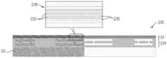
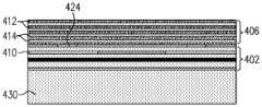
도 1은 본 발명의 일 실시예에 따른, VCSEL(20)의 개략적인 단면도이다.1 is a schematic cross-sectional view of a
VCSEL(20)은 실리콘(Si) 기판(22)과 같은 반도체 기판을 포함한다. Si 기판(22) 상에, 반도체 재료 및 유전체 재료의 교번하는 층들을 포함하는 하위 DBR(24)이 침착되며, 여기서 각각의 층의 두께는 VCSEL(20)에 의해 방출되는 광의 국소 파장의 1/4이다. 고반사율, 예를 들어 99% 반사율을 달성하기 위해, 충분한 수의 층 쌍들이 형성된다. 하위 DBR(24)은, 예를 들어, 반도체 재료로서의 비정질 실리콘(a-Si) 및 유전체 재료로서의 실리콘 이산화물(SiO2)의 교번하는 층들을 포함할 수 있다. 대안적으로 유전체 재료로서 AlN을 사용하면, VCSEL(20)로부터 기판(22)으로의 열 전도율은 SiO2로 달성되는 것보다 실질적으로 증가될 수 있다.The
하위 DBR(24) 위에, n형 InP를 포함하는 하위 접촉부(26)와 p형 InP(p-InP) 층(30) 사이에 개재된 MQW 스택(28)이 있다. 상기에 언급된 바와 같이, MQW 스택(28)은 전형적으로 InxGa1-xAs, InxAlyGa1-x-yAs, InxGa1-xAsyP1-y 및/또는 InxGa1-xAsyN1-y와 같은 양자 우물 재료들을 포함하며, 이때 배리어 층들은 InP, InaAl1-aAs, InaAlbGa1-a-bAs, InaGa1-aAsbP1-b 및/또는 InaGa1-aAsbN1-b를포함한다. p-InP 층(30) 위에는, 구속 층(31)이 있으며, 이어서 상위 n-InP 접촉부(34)가 있다. 도시된 실시예에서의 구속 층(31)은 그의 중심 부분에 BTJ(32)를 포함하며, 이는 그의 주변 부분에서 유전체 충전물(36)로 둘러싸일 수 있다. BTJ(32)는 전형적으로 p+ 층 및 n+ 층의 쌍을 포함하며, 이때 p+ 층이 상위 접촉부(34)에 인접한다. 유전체 충전물(36)은 전형적으로 알루미늄 산화물(Al2O3)을 포함한다. 실리콘 질화물(SiN) 및 a-Si의 교번하는 층들을 포함하는 상위 DBR(38)이 상위 접촉부(34) 위에 침착된다.Above the
대안적인 실시예(도면에 도시되지 않음)에서, 구속 층(31)은, 예를 들어, BTJ 없이, 측방향으로 에칭된 p형 반도체 층을 포함하고, 상위 접촉부(34)는 또한 p형 재료를 포함할 수 있다. 이러한 대안적인 종류의 구속 층을 수용하기 위해 후술되는 공정에서 필요로 되는 변경들이 당업자들에게 명백해질 것이다.In an alternative embodiment (not shown in the drawings), the
VCSEL(20)은 측벽(44)을 갖는 메사형(mesa-type) 구조를 생성하도록 에칭되었다. VCSEL(20)의 메사형 구조는 전형적으로 원통형이고, 그 결과 측벽(44)은 연속적인 원통형 표면이다. 그러나, 대안적인 실시예들은, 예를 들어, 정육면체와 같은 다른 형상들의 메사형 구조를 사용할 수 있고, 그 결과 메사형 구조는 여러 개의 측벽들을 가질 수 있다. 캐소드 및 애노드 전극들(40, 42)은 하위 및 상위 접촉 층들(26, 34) 상에 각각 침착되고 패턴화되어, VCSEL(20)에 대한 여자 전류 경로들을 제공한다. 또한, 원통형 메사형 구조로 인해, 전극들(40, 42)은 동심의 링들이다.
VCSEL(20)의 구조 및 제조 공정에 대한 더 상세한 설명이 하기의 도 2 내지 도 9에서 제공된다.A more detailed description of the structure and fabrication process of the
제조 방법manufacturing method
도 2a 및 도 2b는 함께, 본 발명의 일 실시예에 따른, VCSEL(20)의 제조 공정을 개략적으로 예시하는 흐름도(100)를 제시한다. 핵심 공정 단계들에서 생성된 구조들의 단면도들이 도 3 내지 도 9에 도시되어 있으며, 그들은 흐름도(100)의 적절한 단계들에서 언급될 것이다. 이러한 실시예에서, 하위 DBR(24)이 Si 기판(22)(캐리어 기판) 상에 층들을 침착시킴으로써 형성되고, 한편 VCSEL의 활성 영역을 구성하는 에피택셜 층들이 InP 기판과 같은 III-V족 기판 상에 침착되고, 이어서 하위 DBR에 접합된다. 대안적인 실시예들에서, 도 10a, 도 10b, 및 도 12를 참조하여 후술된 바와 같이, 하위 DBR이 구속 층 및 에피택셜 층들의 세트 위의 III-V족 기판 상에 형성되고, III-V족 기판 상의 이러한 하위 DBR은 이어서 캐리어 기판에 접합된다.2A and 2B together present a flow diagram 100 schematically illustrating a manufacturing process of
제조 공정은 시작 단계(102)로 시작하며, 여기에서부터 제조 공정은 초기에 2개의 병렬 경로들을 따른다. CMOS 단계(104)에서, CMOS 회로들(224)이 Si 기판(22) 상에 제조된다(도 1 및 도 4). 하위 DBR 침착 단계(106)에서, VCSEL(20) 파장에서의 1/4파 두께들을 갖는, SiO2 및 a-Si의 교번하는 층들을 포함하는 다층 구조가 Si 기판(22) 위에 침착되어 하위 DBR(24)을 형성한다. 침착은, 예를 들어, PVD(Physical Vapor Deposition), CVD(Chemical Vapor Deposition), 또는 PECVD(Plasma-Enhanced CVD), 또는 ALD(Atomic Layer Deposition), MOCVD(metal organic CVD), MBE(molecular beam epitaxy), 또는 CBE(chemical beam epitaxy)와 같은 다른 방법들에 의해 수행될 수 있다. 생성된 구조(220)가 도 4에 상세히 나타나있다. 에피-성장 단계(108)에서, 도 3에 상세히 나타낸 바와 같이, 에피택셜 층들이 InP 웨이퍼(202) 상에 성장된다(InGaAs 에칭-정지 층(204)으로 시작함). 다이싱(dicing) 단계(110)에서, InP 웨이퍼(202)가 칩들로 다이싱되며, 여기서 각각의 칩은 나중에 VCSEL(20)이 될 것이다. 단계들(104 내지 106) 및 단계들(108 내지 110)의 2개의 경로들은 접합 단계(112)로 수렴하며, 여기서 각각의 InP 칩이 뒤집혀서 Si 기판(22)에 접합된다. 생성된 구조(240)가 도 5에 상세히 나타나있다.The manufacturing process begins with an
기판 제거 단계(114)에서, InP 웨이퍼(202)의 나머지 부분이 에칭-정지 층(204)에 이르기까지 제거된다. 정지 층 제거 단계(116)에서, 도 3에 도시된 층(204)이 제거된다. 애노드 전극 단계(117)에서, 금속 층이 침착되고 패턴화되어 애노드 전극(42)을 형성한다. 하드 마스크(hard mask) 침착 단계에서, 도 6에 도시된 SiO2 하드 마스크(264)가 상위 접촉부(34) 위에 침착되고 패턴화된다. 제1 메사 에칭 단계(120)에서, 측벽(44)을 갖는 부분적인 메사가 p-InP 층(30)에 이르기까지 에칭된다.In the substrate removal step 114, the remainder of the
도 6에 도시된 바와 같이, 측방향 에칭 단계(122)에서, BTJ(32)는 VCSEL(20)의 오직 코어 부분 내의 제자리에만 남아 있도록 에칭되고, 갭(226)이 상위 접촉부(34)와 p-InP 층(30) 사이에서 파내진다. 도 7에 도시된 바와 같이, 갭 충전 단계(124)에서, Al2O3와 같은 유전체 재료의 충전 층(282)이 ALD를 사용하여 전체 구조 위에 침착된다.As shown in FIG. 6, in a
충전 층 에칭 단계(126)에서, 충전 층(282)의 대부분이 에칭되어, 단지 갭(226)을 충전하는 재료뿐만 아니라 이전에 에칭된 메사 주위의 일부 재료만을 남긴다. 제2 메사 에칭 단계(128)에서, 이전에 에칭된 메사 측벽(44)은 하위 접촉부(26)에 이르기까지 계속된다. SiN 스페이서(spacer) 침착 단계(130)에서 그리고 SiN 스페이서 에칭 단계(132)에서, SiN-층이 각각 침착되고 이어서 에칭되어, 도 8에 도시된 바와 같이, 메사 측 주위에 SiN 스페이서(304)를 형성한다.In the fill
도 8을 추가로 참조하면, 캐소드 전극 단계(134)에서, 캐소드 전극(40)이 침착되고 패턴화된다. 제3 메사 에칭 단계(136)에서, 메사 구조의 측벽(44)이 (도 9에 도시된 바와 같이) 하위 접촉 DBR(24)에 이르기까지 에칭된다. 하드 마스크 에칭 단계(138)에서, 하드 마스크(264)의 대부분이 에칭된다. 상위 DBR 침착 단계(140)에서, 도 1 및 도 8에 상세히 나타낸 바와 같이, 상위 DBR(38)이 SiN 및 a-Si의 교번하는 층들로서 침착된다. 상위 비아 단계(142)에서, 비아들이 캐소드 및 애노드 전극들(40, 42)에 각각 액세스하도록 개방된다. 하위 비아 단계(144)에서, 비아들은 CMOS 회로들(224) 내의 금속 층들에 액세스하도록 개방된다.Referring further to FIG. 8 , in cathode electrode step 134 , a
전도체 침착 단계(146)에서, 전도체들(322, 324)이 RDL(redistribution layer)들로 기능하도록 침착되고 패턴화되어, 애노드 및 캐소드 전극들(42, 40)을 각각 CMOS 회로들(224)에 접속시킨다. 패시베이션 단계(148)에서, SiN이 VCSEL(20) 위에 침착되고, 패드가 수동 층을 통해 개방되어, 칩에 대한 전기 접촉을 가능하게 한다.In
종료 단계(150)가 공정을 끝낸다. 이러한 스테이지에서, Si 기판(22)은 단일 VCSEL들 또는 VCSEL들의 어레이들을 갖는 칩들을 생성하도록 다이싱될 수 있다.An
도 3은, 본 발명의 일 실시예에 따른, 에피-성장 단계(108) 이후의 구조(200)의 개략적인 단면도이다.3 is a schematic cross-sectional view of
구조(200)는, 예를 들어, 3" InP 웨이퍼(202) 상에 제조될 수 있지만, 다른 웨이퍼 직경들이 대안적으로 사용될 수 있다. 제1 InGaAs 정지 층(204)이 InP 웨이퍼(202) 위에 침착된다. 하기의 층들이 InGaAs 정지 층(204) 위에 에피택셜하게 성장되었다: 상위 접촉부(34), BTJ(32), p-InP 층(30), MQW 스택(28), 및 하위 접촉부(26). 에피택셜 층들의 전형적인 총 두께는 2.5 마이크로미터이다. 용어들 "상위" 및 "하위"는, 구조물(200)이 접합 단계(112)에서 뒤집힌 후에 가질 배향에 의해 정의된다.
도 4는, 본 발명의 일 실시예에 따른, CMOS 단계(104) 및 하위 DBR 침착 단계(106) 이후의 구조(220)의 개략적인 단면도이다.4 is a schematic cross-sectional view of
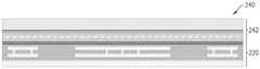
구조(220)는, 예를 들어, 300 mm Si 웨이퍼(22) 상에 제조될 수 있지만, 다른 웨이퍼 직경들이 대안적으로 사용될 수 있다. CMOS 단계(104)에서, 표준 CMOS 공정을 사용하여, CMOS 회로들(224)이 Si 웨이퍼(22) 상에 제조되었다. 하위 DBR 침착 단계(106)에서, 하위 DBR(24)이 CMOS 회로들(224) 위에 침착되었다. 삽도(inset)(228)는 SiO2(230) 및 a-Si(232)의 교번하는 층들을 갖는 하위 DBR(24)의 구조를 도시한다. 층들의 두께들은, 예를 들어, SiO2(230)에 대해서는 224 nm일 수 있고, a-Si(232)에 대해서는 93 nm일 수 있다. 층들의 수는 원하는 수준의 반사율을 달성하도록 선택될 수 있다.
도 5는, 본 발명의 일 실시예에 따른, 접합 단계(112) 이후의 구조(240)의 개략적인 단면도이다.5 is a schematic cross-sectional view of
접합 단계(112)에서, 다이싱 단계(110)에서 구조(200)로부터 생성된 InP 칩(242)이 도 3에 도시된 배향에 대해 뒤집혀서, InP-대-산화물 접합에 의해 구조(220) 상에 접합된다. 대안적으로, 추가의 산화물 층이 InP 위에 침착되면, 직접적인 산화물-대-산화물 접합이 사용될 수 있다.In
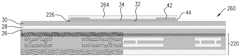
도 6은, 본 발명의 일 실시예에 따른, 측방향 에칭 단계(122) 이후의 구조(260)의 개략적인 단면도이다.6 is a schematic cross-sectional view of
구조(260)는 도 4의 구조(220)뿐만 아니라 도 3의 구조(200)의 하기의 나머지 층들(하부로부터 상부로 나열됨)을 포함한다: 하위 접촉부(26), MQW 스택(28), p-InP 층(30), BTJ(32), 및 상위 접촉부(34). 추가적으로, 구조(260)는 애노드 전극(42) 및 하드 마스크(264)를 포함한다. 상위 접촉부(34) 및 BTJ(32)는 측벽(44)을 갖는 부분적인 메사-구조를 정의하도록 에칭되었고, BTJ(32)는, BTJ의 코어 부분만을 남기면서, p-InP 층(30)과 상위 접촉부(34) 사이의 갭(226)을 파내도록 측방향으로 에칭되었다.
도 7은, 본 발명의 일 실시예에 따른, 갭 충전 단계(124) 이후의 구조(280)의 개략적인 단면도이다.7 is a schematic cross-sectional view of
구조(280)는, 갭(226)을 컨포멀하게(conformally) 충전하도록 구조(260) 위에 침착된 충전 층(282)을 추가한 것을 제외하고는, 도 6의 구조(260)와 동일하다. 충전 층(282)은, 예를들어, 고도로 컨포멀한 ALD 침착 공정을 사용하여 침착된 Al2O3를 포함한다. 대안적으로, 다른 유전체 재료들이 사용될 수 있다.
도 8은, 본 발명의 일 실시예에 따른, 상위 DBR 침착 단계(140) 이후의 구조(300)의 개략적인 단면도이다.8 is a schematic cross-sectional view of
구조(300)는, 연속된 메사 에칭 및 충전 층(282)의 부분적인 에칭 이후의, 도 7의 구조(280)와 동일한 층들을 포함한다. 추가적으로, 구조(300)는 캐소드 전극(40) 및 SiN 스페이서(304)를 포함한다. SiN 및 a-Si의 교번하는 층들을 포함하는 상위 DBR(38)이 구조(300) 위에 침착되었다.
상위 DBR 층들의 두께 및 수들은 설계 목표들에 따른다. 일례로서, 940 nm 목표 VCSEL 파장의 경우, 각각의 a-Si 층의 두께는 약 86 nm이다. 대체적으로, 각각의 층의 두께는 파장/(4.0 * 이러한 파장에서의 재료의 굴절률)과 대략적으로 동일하다. 상위 DBR 선택에 사용되는 재료 쌍들은, 예를 들어, SiN/a-Si, SiO2/a-Si, 또는 AlN/a-Si를 포함할 수 있다(그러나 이에 제한되지 않음). 상위 미러 반사율이 또한 가변할 수 있지만, 대체적으로 그것은 99%를 초과하고, 반면 하위 DBR의 것은 대체적으로 99.9%를 초과한다. 이러한 반사율 범위에 도달하기 위해서는 대체적으로 적어도 3개의 쌍들의 교번하는 SiO2/a-Si 또는 다른 DBR 재료들이 요구된다. 대안적으로, 2개의 쌍들의 AlN/a-Si 및 다른 2개의 쌍들의 SiO2/a-Si를 사용하여 이러한 반사율 범위에 도달하는 것이 가능하다.The thickness and number of upper DBR layers depend on design goals. As an example, for a target VCSEL wavelength of 940 nm, the thickness of each a-Si layer is about 86 nm. In general, the thickness of each layer is approximately equal to wavelength/(4.0 * the index of refraction of the material at that wavelength). Material pairs used in the upper DBR selection may include, but are not limited to, SiN/a-Si, SiO2 /a-Si, or AlN/a-Si, for example. The upper mirror reflectivity can also vary, but typically it exceeds 99%, while that of the lower DBR typically exceeds 99.9%. Typically at least three pairs of alternating SiO2 /a-Si or other DBR materials are required to reach this reflectivity range. Alternatively, it is possible to reach this reflectance range using two pairs of AlN/a-Si and the other two pairs of SiO2 /a-Si.
SiN 스페이서(304)의 층 두께는 수십 나노미터 내지 수백 나노미터, 또는 심지어 그 이상일 수 있다. 대안적으로, 스페이서 층은, 예를 들어, SiO2, AlOx, 또는 AlN과 같은 (그러나 이에 제한되지 않는) SiN 이외의 재료들로 만들어질 수 있다.The layer thickness of the
도 9는, 본 발명의 일 실시예에 따른, 패시베이션 단계(148) 이후의 완성된 VCSEL(20)의 개략적인 단면도이다.9 is a schematic cross-sectional view of the completed
VCSEL(20)은 도 8의 구조(300)와 유사하며, 이때 애노드 전극(42) 및 캐소드 전극(40)을 단계들(142 및 144)에서 개방된 비아들을 통해 CMOS 회로들(224)에 각각 접속시키기 위해 애노드 전도체(322) 및 캐소드 전도체(324)가 추가되었다. VCSEL(20)은 SiN 패시베이션 층(326)으로 추가로 코팅된다.
대안적인 실시예들alternative embodiments
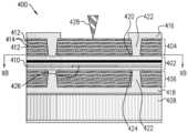
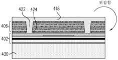
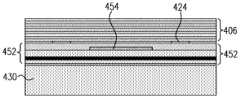
도 10a 및 도 10b는, 본 발명의 다른 실시예에 따른, VCSEL(400)의 개략적인 단면도들이다. 도 10a는 선행하는 도면에서와 같은 측단면도이고, 한편 도 10b는 도 10a의 선 XB-XB를 따라 취해진 정면 단면도이다. 이러한 실시예뿐만 아니라 도 12에 도시된 실시예는, 후술되는 소정 차이점들을 제외하고는, 전술된 실시예에 대한 구조 및 제조의 재료들 및 원리들에서 유사하다. 간결함을 위해, 하기의 설명은 이들 차이점들에 초점을 맞출 것이다.10A and 10B are schematic cross-sectional views of a
VCSEL(400)은, 선행하는 실시예에서와 같이, 양자 우물 구조 및 구속 층(410)을 포함하는, 활성 영역(402)을 구성하는 에피택셜 층들을 포함한다. (도 11c에 도시된 바와 같이) 하위 DBR(406)이 활성 영역(402)의 층들 위의 III-V족 반도체 기판 상에 형성되고, 이어서 캐리어 기판(408)에 접합된다. 캐리어 기판은, 선행하는 실시예에서와 같이, Si 웨이퍼와 같은 반도체 재료를, 또는 AlN 웨이퍼와 같은 유전체 재료를 포함할 수 있다. 캐리어 기판에 접합한 후에, III-V족 웨이퍼가 제거되고, 이어서 상위 DBR(404)이 활성 영역(402) 위에 침착된다. 선행하는 실시예에서와 같이, 하위 DBR(406) 및 상위 DBR(404) 둘 모두는 a-Si, 및 SiO2 또는 AlN과 같은 유전체 재료의 교번하는 층들(412, 414)을 포함한다.
이러한 방식으로 III-V족 웨이퍼 상에 상위 및 하위 DBR 스택들 둘 모두를 침착하는 것은, 선행하는 실시예에서와 같이 캐리어 웨이퍼 상에 하위 DBR 스택을 침착하는 것에 비해, 제작역량(manufacturability)을 향상시키고 공정 수율을 증가시킨다는 관점에서 유익하다. 다른 이점들 중에서, VCSEL(400)의 설계는 매우 얇은 조각의 III-V족 웨이퍼를 다룰 필요성을 배제시켜, 웨이퍼 파손으로 인한 수율의 손실을 감소시킨다. 본 실시예에서, 활성 영역(402)은 매우 얇게 만들어질 수 있어서, 열 발산을 용이하게 한다.Depositing both the upper and lower DBR stacks on a III-V wafer in this way improves manufacturability compared to depositing the lower DBR stack on a carrier wafer as in the preceding embodiment. It is beneficial from the point of view of increasing the process yield and increasing the process yield. Among other benefits, the design of
열 발산을 추가로 용이하게 하기 위해, VCSEL(400)은 활성 영역(402)에 근접하게 (즉, VCSEL 내의 발열 양자 우물 구조에 가깝게) 금속 링 전극들(420, 424)을 포함한다. 도시된 실시예에서의 링 전극들(420, 424)은 각각 DBR들(404, 406) 아래에 침착되고, 금속 비아들(422)에 의해 DBR 층들(412, 414)의 스택들을 통해 전기 접촉부들(416, 418)에 각각 접속된다. 링 전극들은 높은 전기 전도율 및 높은 열 전도율 둘 모두를 갖는 금속, 예를 들어, 금을 포함한다. 그들은 활성 영역(402)에 여자 전류를 전달하고 활성 영역으로부터 열을 제거하는 이중 목적을 제공하며, 따라서 접합부 온도를 낮추고 VCSEL의 벽-플러그(wall-plug) 효율을 증가시킨다. 단지 2개의 비아들(422)이 도 10b의 단면도에 도시되어 있지만, 더 많은 수의 비아들이 열 방출의 목적을 위해 필요에 따라 형성될 수 있다. 대안적인 실시예(도면에 도시되지 않음)에서, 이러한 종류의 링 전극은 활성 영역(402)의 일 측 상에만 내장될 수 있으며, 이때 (예를 들어, 선행하는 실시예에서와 같은) 외부 전극은 다른 측 상에 있다.To further facilitate heat dissipation,
선행하는 실시예에서와 같이, 구속 층(410)은 III-V족 반도체 재료를 포함하는 중심 부분(426)을 포함하고, 이때 주변 부분은 중심 부분을 둘러싸며 유전체 재료를 포함한다. 전극들(420, 424) 사이를 흐르는 전류는, 양자 우물 구조에 의해 생성되는 광학 에너지이기 때문에, 이러한 중심 부분(426)을 통해 채널링되어(channeled), 잘 제어된 출력 빔(428)을 발생시킨다.As in the preceding embodiments,
도 11a, 도 11b, 도 11c, 도 11d, 도 11e, 및 도 11f는, 본 발명의 일 실시예에 따른, VCSEL(400)의 제조 공정의 연속적인 단계들에서 형성된 구조들의 개략적인 단면도들이다.11A, 11B, 11C, 11D, 11E, and 11F are schematic cross-sectional views of structures formed in successive stages of a manufacturing process of
도 11a에 도시된 바와 같이, 활성 영역(402)이 InP 웨이퍼와 같은 III-V족 반도체 기판(430) 상에 에피택셜 층들의 성장에 의해 형성된다. 금속 층이 활성 영역(402) 위에 침착되고 패턴화되어, 링 전극(424)을 정의한다. 초기 메사 에칭이 또한 (도 2a의 단계(120)에서와 같은) 이러한 스테이지에서 수행될 수 있다. 이어서, 구속 층(410)이 (단계(122)에서와 같이) 측방향으로, 예를 들어, 습식 에칭 공정으로 에칭되어, 반도체 재료를 중심 부분(426)에만 남긴다. 도 11b에 도시된 바와 같이, 주변 부분이, 예를 들어, ALD에 의해 유전체 재료(434)로 충전된다.As shown in FIG. 11A, an
다음으로, 도 11c에 도시된 바와 같이, 하위 DBR(406)이 (이 도면에 도시되지 않은, SiN의 기저(underlying) 에칭-정지 층과 함께) 층들(412, 414)을 교번하여 침착시킴으로써 활성 영역(402) 및 링 전극(424) 위에 형성된다. 하위 DBR(406)이 하위 DBR(406)을 통한 비아들(422)을 정의하도록 패턴화된다. 적합한 배리어 층(도시되지 않음)의 침착 및 에칭에 이어서, 금속, 예를 들어 금이 비아들 내에 그리고 DBR(406)의 외부 표면 위에 침착된다. 따라서, 도 11d에 도시된 바와 같이, 비아들(422)은, 전기적 및 열적 둘 모두로, 링 전극(424)을 전기 접촉부(418)에 접속시킨다.Next, as shown in FIG. 11C, a
도 11e에 도시된 바와 같이, III-V족 반도체 기판(430)이 이제 뒤집혀, 캐리어 웨이퍼(408)에 접합된다. 기판들은, 예를 들어, 전기 접촉부(418)의 Au를 캐리어 웨이퍼의 표면 상의 적합한 층, 예컨대 Au 또는 Au-함유 땜납의 층에 접합함으로써, 또는 적합한 접착제를 사용함으로써 함께 접합될 수 있다. 이러한 접합 단계 이후에만, 예를 들어, 습식 에칭에 의해 기판(430)이 제거된다. 이어서, 도 11f에 도시된 바와 같이, 링 전극(420)이 활성 영역(402)의 외부 표면 상에 침착되고, 뒤이어 상위 DBR(404)의 층들의 스택이 침착되고, 이어서 금속 충전물이 에칭되어, 비아들 및 전기 접촉부(416)를 형성한다. 이러한 후자의 단계들은, 필요한 부분만 약간 수정하여, 도 11c 및 도 11d를 참조하여 전술된 것들과 유사하다. 전기 접촉부(416)의 금속은 VCSEL의 광학 개구부를 노출시키도록 제거된다.As shown in FIG. 11E , the III-
본 발명자들은 VCSEL 내의 재료들의 열 속성들에 기초하여, VCSEL(400)의 동작 동안의 열 발산을 연구했다. 활성 영역(402) 내의 열의 대부분은 링 전극들(420, 424)을 향해 측방향으로 바깥쪽으로 흐르고; 이어서 비아들(422)은 열을 상위 및 하위 금속 접촉 층들로 전도한다. 공칭(nominal) 출력 파워 및 실내 온도에서의 VCSEL(400)의 연속파(continuous wave, CW) 동작에서, 활성 영역(402) 내의 온도는 적정하게, 예를 들어, 일부 설계들에서 약 50℃를 초과하지 않게 유지되는 반면, DBR들(404, 406)의 외부 표면들은 실질적으로 더 냉각된다. 링 전극들 및 비아들의 냉각 효과는 VCSEL의 전기 효율 및 수명을 향상시킬 뿐만 아니라, VCSEL의 접합 및 패키징을 위한 공정 요건들을 단순화시킨다.The inventors studied the heat dissipation during operation of the
도 12는, 본 발명의 또 다른 실시예에 따른, VCSEL(450)의 개략적인 단면도이다. VCSEL(450)은, VCSEL(450)의 활성 영역(452) 내의 구속 층이 (VCSEL(400)에서와 같은 측방향 에칭 및 유전체 충전의 공정보다는) 에피택셜 재성장의 공정에 의해 형성되는 BTJ(454)를 포함한다는 것을 제외하고는, 앞서 도시되고 전술된 바와 같은, VCSEL(400)에 대한 그것의 구조 및 동작의 원리들에서 유사하다. 이러한 종류의 구속 층은 재성장 공정의 양호한 제어를 요구하지만, 선행하는 실시예에서 사용되는 측방향 에칭 공정에서의 에칭 부정확성의 문제들을 회피한다.12 is a schematic cross-sectional view of a
도 13a, 도 13b, 및 도 13c는, 본 발명의 일 실시예에 따른, VCSEL(450)의 (그리고 구체적으로 활성 영역(452)의) 제조 공정의 연속적인 단계들에서 형성된 구조들의 개략적인 단면도들이다. 도 13a에 도시된 바와 같이, BTJ(454)는 활성 영역(452)의 양자 우물 구조 위의 저농도로 도핑된 p형(p-) 반도체 층 위에 고농도로 도핑된 p형(p++) 반도체의 층을 에피택셜하게 성장시킴으로써 형성된다. P++ 층은 (저농도로 도핑된 p형 반도체 층에서 정지하기 위한) 원하는 깊이 및 (VCSEL의 전류 개구부를 형성하기 위한) 원하는 측방향 치수들로 에칭된다. 이어서, 고농도로 도핑된 n형(n++) 반도체의 층(456)이 패턴화된 p++ 반도체 위에 그리고 그 주위에서 재성장되고, 따라서 BTJ 및 구속 층을 생성한다. 도 13b에 도시된 바와 같이, 금속 층이 층(456) 위에 침착되고, 이어서 링 전극(424)을 형성하도록 에칭된다. 도 13c에 도시된 바와 같이, 하위 DBR(406)이 링 전극(424) 및 활성 영역(452) 위에 침착된다. 공정은 이어서 도 11d, 도 11e, 및 도 11f를 참조하여 전술된 방식으로 계속된다.13A, 13B, and 13C are schematic cross-sectional views of structures formed in successive stages of a fabrication process of VCSEL 450 (and specifically of active region 452), according to one embodiment of the present invention. admit. As shown in FIG. 13A,
전술된 실시예들은 예로서 인용되어 있고 본 발명은 위에서 구체적으로 도시되고 기술된 것으로 제한되지 않는다는 것이 이해될 것이다. 오히려, 본 발명의 범주는 위에서 기술된 다양한 특징들의 조합들 및 하위조합들 양측 모두를 포함할 뿐만 아니라, 전술된 설명을 읽을 때 당업자에게 생각이 떠오를 것이고 종래 기술에서 개시되지 않은 변형들 및 변경들도 포함한다.It will be understood that the foregoing embodiments are cited as examples and that the present invention is not limited to that specifically shown and described above. Rather, the scope of the present invention includes both combinations and subcombinations of the various features described above, as well as modifications and variations not disclosed in the prior art that will occur to those skilled in the art upon reading the foregoing description. Also includes
Claims (20)
Translated fromKorean캐리어 기판;
상기 기판의 구역 상에 배치되고 교번하는 제1 유전체 층 및 반도체 층을 포함하는 하위 분포 브래그 반사기(distributed Bragg-reflector, DBR) 스택;
상기 하위 DBR 위에 배치된 에피택셜 층(epitaxial layer)들의 세트 - 상기 에피택셜 층들의 세트는 하나 이상의 III-V족 반도체 재료들을 포함하고,
양자 우물 구조; 및
구속 층(confinement layer)을 정의함 -;
상기 에피택셜 층들의 세트 위에 배치되고, 교번하는 제2 유전체 층 및 반도체 층을 포함하는 상위 DBR 스택;
상기 양자 우물 구조에 여자 전류를 인가하도록 커플링된 전극들 - 상기 전극들 중 적어도 하나는 상기 양자 우물 구조에 근접하게 배치된 금속 링을 포함함 -; 및
상기 DBR 스택들 중 적어도 하나의 내측에 있는 상기 금속 링을 상기 DBR 스택들 중 적어도 하나의 외측 상의 전기 접촉부에 접속시키기 위해 상기 DBR 스택들 중 적어도 하나를 관통하는 하나 이상의 금속 비아(via)들을 포함하는, 광전자 디바이스.As an optoelectronic device,
carrier substrate;
a sub-distributed Bragg-reflector (DBR) stack disposed on a region of the substrate and comprising alternating first dielectric layers and semiconductor layers;
a set of epitaxial layers disposed over the lower DBR, the set of epitaxial layers comprising one or more III-V semiconductor materials;
quantum well structure; and
define the confinement layer -;
an upper DBR stack disposed over the set of epitaxial layers and comprising alternating second dielectric layers and semiconductor layers;
electrodes coupled to apply an excitation current to the quantum well structure, at least one of the electrodes comprising a metal ring disposed proximate to the quantum well structure; and
one or more metal vias through at least one of the DBR stacks to connect the metal ring on the inside of at least one of the DBR stacks to an electrical contact on the outside of at least one of the DBR stacks. , optoelectronic devices.
III-V족 반도체 재료를 포함하는 중심 부분; 및
상기 중심 부분을 둘러싸고 유전체 재료를 포함하는 주변 부분을 포함하는, 광전자 디바이스.7. The method according to any one of claims 1 to 6, wherein the confinement layer comprises:
a central portion comprising a III-V semiconductor material; and
and a peripheral portion surrounding the central portion and comprising a dielectric material.
양자 우물 구조를 형성하기 위해 III-V족 기판 상에 III-V족 반도체 재료들을 포함하는 에피택셜 층들의 세트를 침착하는 단계;
상기 양자 우물 구조 위에 구속 층을 형성하는 단계;
하위 분포 브래그 반사기(DBR) 스택을 형성하기 위해 교번하는 제1 유전체 층 및 반도체 층을 침착하는 단계;
상기 하위 DBR 스택이 상기 양자 우물 구조와 캐리어 기판 사이에 위치되도록 상기 III-V족 기판을 상기 캐리어 기판에 접합시키고, 이어서 상기 III-V족 기판을 제거하는 단계;
상기 III-V족 기판을 제거한 후에, 상위 DBR 스택을 형성하기 위해, 교번하는 제2 유전체 층 및 반도체 층을 상기 에피택셜 층들의 세트 위에 침착하는 단계; 및
상기 상위 DBR 스택을 형성하기 전에, 상기 양자 우물 구조의 적어도 하나의 측 위에 금속 링을 침착하고, 상기 DBR 스택들 중 적어도 하나의 내측에 있는 상기 금속 링을 상기 DBR 스택들 중 적어도 하나의 외측 상의 전기 접촉부에 접속시키기 위해, 상기 DBR 스택들 중 적어도 하나를 관통하는 하나 이상의 금속 비아들을 형성하는 것에 의해 상기 양자 우물 구조에 여자 전류를 인가하도록 전극들을 커플링하는 단계를 포함하는, 방법.As a method for manufacturing an optoelectronic device,
depositing a set of epitaxial layers comprising III-V semiconductor materials on a III-V substrate to form a quantum well structure;
forming a confinement layer over the quantum well structure;
depositing alternating first dielectric and semiconductor layers to form a lower distributed Bragg reflector (DBR) stack;
bonding the group III-V substrate to the carrier substrate so that the lower DBR stack is positioned between the quantum well structure and the carrier substrate, and then removing the group III-V substrate;
after removing the III-V substrate, depositing alternating second dielectric layers and semiconductor layers over the set of epitaxial layers to form an upper DBR stack; and
Prior to forming the upper DBR stack, a metal ring is deposited on at least one side of the quantum well structure, and the metal ring on the inside of at least one of the DBR stacks is placed on the outside of at least one of the DBR stacks. coupling electrodes to apply an excitation current to the quantum well structure by forming one or more metal vias through at least one of the DBR stacks to connect to an electrical contact.
Applications Claiming Priority (3)
| Application Number | Priority Date | Filing Date | Title |
|---|---|---|---|
| US201962808314P | 2019-02-21 | 2019-02-21 | |
| US62/808,314 | 2019-02-21 | ||
| PCT/US2020/018475WO2020172077A1 (en) | 2019-02-21 | 2020-02-17 | Indium-phosphide vcsel with dielectric dbr |
Publications (2)
| Publication Number | Publication Date |
|---|---|
| KR20210115020A KR20210115020A (en) | 2021-09-24 |
| KR102518449B1true KR102518449B1 (en) | 2023-04-05 |
Family
ID=69784616
Family Applications (1)
| Application Number | Title | Priority Date | Filing Date |
|---|---|---|---|
| KR1020217026188AActiveKR102518449B1 (en) | 2019-02-21 | 2020-02-17 | Indium Phosphide VCSEL with Dielectric DBR |
Country Status (5)
| Country | Link |
|---|---|
| US (2) | US11322910B2 (en) |
| EP (1) | EP3888138A1 (en) |
| KR (1) | KR102518449B1 (en) |
| CN (2) | CN113396486B (en) |
| WO (1) | WO2020172077A1 (en) |
Families Citing this family (14)
| Publication number | Priority date | Publication date | Assignee | Title |
|---|---|---|---|---|
| US11322910B2 (en)* | 2019-02-21 | 2022-05-03 | Apple Inc. | Indium-phosphide VCSEL with dielectric DBR |
| JP7631324B2 (en)* | 2019-09-18 | 2025-02-18 | エルファウンドリー エッセ.エッレ.エッレ | Method for manufacturing back-illuminated optical sensor with improved detection parameters |
| US11880052B2 (en) | 2020-11-20 | 2024-01-23 | Applied Materials, Inc. | Structure and method of mirror grounding in LCoS devices |
| US12055821B2 (en) | 2020-11-20 | 2024-08-06 | Applied Materials, Inc. | Structure and method of bi-layer pixel isolation in advanced LCOS back-plane |
| US11881539B2 (en)* | 2020-11-20 | 2024-01-23 | Applied Materials, Inc. | Structure and method of advanced LCoS back-plane having highly reflective pixel via metallization |
| US11611195B2 (en)* | 2020-12-30 | 2023-03-21 | Mellanox Technologies, Ltd. | Fabrication of low-cost long wavelength VCSEL with optical confinement control |
| US11908678B2 (en) | 2021-01-14 | 2024-02-20 | Applied Materials, Inc. | Method of CMP integration for improved optical uniformity in advanced LCOS back-plane |
| JP7742724B2 (en) | 2021-06-07 | 2025-09-22 | スタンレー電気株式会社 | Vertical cavity light emitting device and its manufacturing method |
| US20250070531A1 (en)* | 2022-01-07 | 2025-02-27 | Sony Group Corporation | Surface emitting laser |
| CN114759432A (en)* | 2022-03-15 | 2022-07-15 | 浙江焜腾红外科技有限公司 | Lens-free VCSEL flip chip |
| US20240039247A1 (en)* | 2022-07-28 | 2024-02-01 | Ams International Ag | Optoelectronic semiconductor device and method for operating an optoelectronic semiconductor device |
| DE102023116537A1 (en)* | 2023-06-23 | 2024-12-24 | Ams-Osram International Gmbh | METHOD FOR PRODUCING A PLURALITY OF SEMICONDUCTOR LASER CHIP, SEMICONDUCTOR LASER CHIP, METHOD FOR PRODUCING A LASER COMPONENT AND LASER COMPONENT |
| EP4528945A1 (en)* | 2023-09-22 | 2025-03-26 | Changchun Institute of Optics, Fine Mechanics and Physics, Chinese Academy of Sciences | Radiation emitter and method of fabricating radiation emitters |
| WO2025197672A1 (en)* | 2024-03-19 | 2025-09-25 | ソニーグループ株式会社 | Light emitting device |
Citations (4)
| Publication number | Priority date | Publication date | Assignee | Title |
|---|---|---|---|---|
| US20020150130A1 (en)* | 2001-04-16 | 2002-10-17 | Coldren Larry A. | Tunable VCSEL assembly |
| WO2018053378A1 (en)* | 2016-09-19 | 2018-03-22 | Montrose Laboratories Llc | Vertical emitters integrated on silicon control backplane |
| US20180241177A1 (en)* | 2017-01-30 | 2018-08-23 | Oepic Semiconductors, Inc. | Tunnel junction for gasa based vcsels and method therefore |
| US20180287345A1 (en)* | 2017-04-04 | 2018-10-04 | Apple Inc. | VCSELs with improved optical and electrical confinement |
Family Cites Families (110)
| Publication number | Priority date | Publication date | Assignee | Title |
|---|---|---|---|---|
| DE10353951A1 (en) | 2003-11-18 | 2005-06-16 | U-L-M Photonics Gmbh | Polarization control of vertical diode lasers by a monolithically integrated surface grid |
| US5500540A (en) | 1994-04-15 | 1996-03-19 | Photonics Research Incorporated | Wafer scale optoelectronic package |
| US5940113A (en) | 1994-12-19 | 1999-08-17 | Xerox Corporation | Lensless printing system with a light bar printhead |
| KR970031126A (en) | 1995-11-13 | 1997-06-26 | 빈센트 비. 인그라시아 | Low resistance p-down top radial ridge vertical. Low resistance p-down top emitting ridge VCSEL and method of fabrication |
| US5719891A (en) | 1995-12-18 | 1998-02-17 | Picolight Incorporated | Conductive element with lateral oxidation barrier |
| JP3236774B2 (en) | 1996-02-16 | 2001-12-10 | 日本電信電話株式会社 | Semiconductor integrated circuit |
| JP2871623B2 (en) | 1996-07-11 | 1999-03-17 | 日本電気株式会社 | Semiconductor laser device |
| US6014400A (en) | 1996-09-02 | 2000-01-11 | Matsushita Electric Industrial Co., Ltd | Surface-emitting laser and a fabrication method thereof |
| JPH10173294A (en) | 1996-10-07 | 1998-06-26 | Canon Inc | Compound semiconductor multilayer mirror containing nitrogen and surface light emitting device using the same |
| JPH11154774A (en) | 1997-08-05 | 1999-06-08 | Canon Inc | Method for manufacturing surface-emitting semiconductor device, surface-emitting semiconductor device manufactured by this method, and display device using this device |
| JPH11168263A (en) | 1997-09-30 | 1999-06-22 | Canon Inc | Optical device and manufacturing method thereof |
| JP3333747B2 (en) | 1998-01-19 | 2002-10-15 | 學校法人浦項工科大學校 | Optical quantum ring laser diode and target angle measuring device |
| DE19813727C2 (en) | 1998-03-27 | 2000-04-13 | Siemens Ag | Vertical resonator laser diode and process for its manufacture |
| US6117699A (en) | 1998-04-10 | 2000-09-12 | Hewlett-Packard Company | Monolithic multiple wavelength VCSEL array |
| JP3713956B2 (en) | 1998-05-29 | 2005-11-09 | 富士ゼロックス株式会社 | Manufacturing method of surface emitting semiconductor laser device |
| US6181717B1 (en) | 1999-06-04 | 2001-01-30 | Bandwidth 9 | Tunable semiconductor laser system |
| JP2001036397A (en) | 1999-07-22 | 2001-02-09 | Sanyo Electric Co Ltd | Input buffer |
| JP3990846B2 (en) | 1999-08-27 | 2007-10-17 | キヤノン株式会社 | Planar optical element, method for manufacturing the same, and apparatus using the same |
| US6344664B1 (en) | 1999-12-02 | 2002-02-05 | Tera Connect Inc. | Electro-optical transceiver system with controlled lateral leakage and method of making it |
| US6583445B1 (en) | 2000-06-16 | 2003-06-24 | Peregrine Semiconductor Corporation | Integrated electronic-optoelectronic devices and method of making the same |
| KR100384598B1 (en) | 2000-11-29 | 2003-05-22 | 주식회사 옵토웰 | Nitride compound semiconductor vertical-cavity surface-emitting laser |
| US6549556B1 (en)* | 2000-12-01 | 2003-04-15 | Applied Optoelectronics, Inc. | Vertical-cavity surface-emitting laser with bottom dielectric distributed bragg reflector |
| KR100345452B1 (en) | 2000-12-14 | 2002-07-26 | 한국전자통신연구원 | Long-wavelength vertical-cavity surface-emitting laser device having diffusion area in edge of upper mirror and method for forming the same |
| US6589805B2 (en) | 2001-03-26 | 2003-07-08 | Gazillion Bits, Inc. | Current confinement structure for vertical cavity surface emitting laser |
| US6628694B2 (en) | 2001-04-23 | 2003-09-30 | Agilent Technologies, Inc. | Reliability-enhancing layers for vertical cavity surface emitting lasers |
| JP2003121611A (en) | 2001-10-16 | 2003-04-23 | Canon Inc | Lens made of semiconductor material containing Al, surface-type optical element using the same, and method of manufacturing lens |
| JP4066654B2 (en) | 2001-12-19 | 2008-03-26 | 富士ゼロックス株式会社 | Surface emitting semiconductor laser device and manufacturing method thereof |
| US6455340B1 (en) | 2001-12-21 | 2002-09-24 | Xerox Corporation | Method of fabricating GaN semiconductor structures using laser-assisted epitaxial liftoff |
| US6798806B1 (en) | 2002-09-03 | 2004-09-28 | Finisar Corporation | Hybrid mirror VCSELs |
| KR100523484B1 (en) | 2002-11-11 | 2005-10-24 | 한국전자통신연구원 | Method for fabricating semiconductor optical devices having current-confined structure |
| KR100487224B1 (en) | 2002-12-18 | 2005-05-03 | 삼성전자주식회사 | Vertical cavity surface emitting laser and method for fabricating the same |
| US6963119B2 (en) | 2003-05-30 | 2005-11-08 | International Business Machines Corporation | Integrated optical transducer assembly |
| CN1283030C (en) | 2003-08-20 | 2006-11-01 | 和心光通科技股份有限公司 | Array type single transverse mode surface emitting laser device and manufacturing method thereof |
| JP2005159071A (en) | 2003-11-27 | 2005-06-16 | Ricoh Co Ltd | Semiconductor device, manufacturing method thereof, and optical transmission system |
| US20050189551A1 (en) | 2004-02-26 | 2005-09-01 | Hui Peng | High power and high brightness white LED assemblies and method for mass production of the same |
| JP4116587B2 (en) | 2004-04-13 | 2008-07-09 | 浜松ホトニクス株式会社 | Semiconductor light emitting device and manufacturing method thereof |
| US7564887B2 (en) | 2004-06-30 | 2009-07-21 | Finisar Corporation | Long wavelength vertical cavity surface emitting lasers |
| DE102004032696A1 (en) | 2004-07-06 | 2006-02-16 | Universität Ulm | Surface-emitting semiconductor laser with lateral heat dissipation |
| US20060013276A1 (en) | 2004-07-15 | 2006-01-19 | Mchugo Scott A | VCSEL having an air gap and protective coating |
| US7242027B2 (en) | 2004-08-13 | 2007-07-10 | Paul Steven Schranz | Light emitting and image sensing device and apparatus |
| CN1632958A (en) | 2005-01-10 | 2005-06-29 | 金芃 | Novel vertical structure gallium nitride base semiconductor LED and manufacturing technique thereof |
| US7376169B2 (en)* | 2005-03-07 | 2008-05-20 | Joseph Reid Henrichs | Optical phase conjugation laser diode |
| JP4839662B2 (en) | 2005-04-08 | 2011-12-21 | 富士ゼロックス株式会社 | Surface emitting semiconductor laser array and optical transmission system using the same |
| JP5017797B2 (en) | 2005-04-18 | 2012-09-05 | 富士ゼロックス株式会社 | Multi-spot surface emitting laser and driving method thereof |
| JP2008543098A (en) | 2005-06-08 | 2008-11-27 | ファイアカムズ・リミテッド | Surface emitting optical device |
| FR2888405B1 (en) | 2005-07-08 | 2007-10-26 | Alcatel Sa | OPTOELECTRONIC DEVICE COMPRISING AN INTEGRATED LASER AND MODULATOR AND METHOD FOR MAKING THE SAME |
| US20070091961A1 (en) | 2005-10-07 | 2007-04-26 | Chao-Kun Lin | Method and structure for low stress oxide VCSEL |
| JP5034662B2 (en) | 2006-06-20 | 2012-09-26 | ソニー株式会社 | Surface emitting semiconductor laser and manufacturing method thereof |
| CN101026211B (en) | 2006-11-30 | 2011-02-09 | 金芃 | Conductive support substrate through-hole vertical structure semiconductor chip or device |
| JP2009094308A (en) | 2007-10-10 | 2009-04-30 | Fuji Xerox Co Ltd | Semiconductor light emitting module |
| JP4639249B2 (en) | 2008-07-31 | 2011-02-23 | キヤノン株式会社 | Surface emitting laser manufacturing method, surface emitting laser array manufacturing method, surface emitting laser, surface emitting laser array, and optical apparatus including surface emitting laser array |
| CN101667716B (en)* | 2008-09-03 | 2011-10-26 | 中国科学院半导体研究所 | Double-sided bonding long-wavelength vertical cavity surface emitting laser and manufacturing method thereof |
| CN101447647B (en) | 2008-12-22 | 2010-08-11 | 中国科学院长春光学精密机械与物理研究所 | Series connection structure of vertical cavity surface emitting laser array |
| US10038304B2 (en) | 2009-02-17 | 2018-07-31 | Trilumina Corp. | Laser arrays for variable optical properties |
| JP2010192650A (en) | 2009-02-18 | 2010-09-02 | Fuji Xerox Co Ltd | Surface-emitting semiconductor laser, surface-emitting semiconductor laser device, optical transmission apparatus, and optical information processing apparatus |
| JP2011151293A (en) | 2010-01-25 | 2011-08-04 | Fuji Xerox Co Ltd | Surface emission semiconductor laser, surface emission semiconductor laser device, optical transmission device, and information processor |
| US20110187878A1 (en) | 2010-02-02 | 2011-08-04 | Primesense Ltd. | Synchronization of projected illumination with rolling shutter of image sensor |
| US9825425B2 (en) | 2013-06-19 | 2017-11-21 | Apple Inc. | Integrated structured-light projector comprising light-emitting elements on a substrate |
| CN101841129B (en) | 2010-05-24 | 2011-06-29 | 中国科学院长春光学精密机械与物理研究所 | Monolithic integrated phase-locked surface emitting distributed feedback semiconductor laser array |
| US8654811B2 (en) | 2010-08-25 | 2014-02-18 | Flir Systems, Inc. | Serially interconnected vertical-cavity surface emitting laser arrays |
| CN102013633B (en)* | 2010-10-29 | 2012-06-13 | 北京工业大学 | Bridge type nano grating tunable vertical cavity surface emitting laser and preparation method thereof |
| WO2012068467A2 (en) | 2010-11-19 | 2012-05-24 | University Of Delaware | Hybrid dielectric - metallic back surface reflector for photovoltaic applications |
| US8520114B2 (en) | 2011-06-01 | 2013-08-27 | Global Oled Technology Llc | Apparatus for displaying and sensing images |
| CN102354712A (en) | 2011-06-24 | 2012-02-15 | 中国科学院上海微系统与信息技术研究所 | Wide spectrum high reflectivity irregularly shaped distributed Brag reflector (IDBR) and manufacturing method thereof |
| US8749796B2 (en) | 2011-08-09 | 2014-06-10 | Primesense Ltd. | Projectors of structured light |
| JP5558446B2 (en) | 2011-09-26 | 2014-07-23 | 株式会社東芝 | Photoelectric conversion device and manufacturing method thereof |
| JP5425172B2 (en) | 2011-12-15 | 2014-02-26 | ソニー株式会社 | Semiconductor laser device and manufacturing method of semiconductor laser device |
| CN104160240B (en) | 2012-02-15 | 2017-02-22 | 苹果公司 | Scanning depth engine |
| US9036956B2 (en) | 2012-02-17 | 2015-05-19 | Haynes and Boone, LLP | Method of fabricating a polymer waveguide |
| JP5999304B2 (en) | 2012-02-17 | 2016-09-28 | 株式会社リコー | Optical sensor and image forming apparatus |
| CN103378239B (en) | 2012-04-25 | 2016-06-08 | 清华大学 | Epitaxial structure |
| US8822275B2 (en) | 2012-04-30 | 2014-09-02 | Hewlett-Packard Development Company, L.P. | Composite wafer including a molded wafer and a second wafer |
| KR20140061117A (en) | 2012-11-13 | 2014-05-21 | 유태경 | Lighting device and sensor module comprising led chip with vcsel or rcled |
| DE102012112530A1 (en) | 2012-12-18 | 2014-06-18 | Osram Opto Semiconductors Gmbh | Method for producing optoelectronic semiconductor chips and optoelectronic semiconductor chip |
| CN103050063B (en) | 2012-12-24 | 2015-10-21 | 中国科学院西安光学精密机械研究所 | High-brightness traffic variable information board and implementation method thereof |
| US9666702B2 (en) | 2013-03-15 | 2017-05-30 | Matthew H. Kim | Advanced heterojunction devices and methods of manufacturing advanced heterojunction devices |
| WO2015011984A1 (en) | 2013-07-22 | 2015-01-29 | 株式会社村田製作所 | Vertical-cavity surface-emitting laser array, and production method therefor |
| JP6137318B2 (en) | 2013-07-22 | 2017-05-31 | 株式会社村田製作所 | Vertical cavity surface emitting laser array |
| US9038883B2 (en) | 2013-09-11 | 2015-05-26 | Princeton Optronics Inc. | VCSEL packaging |
| US9520696B2 (en) | 2014-03-04 | 2016-12-13 | Princeton Optronics Inc. | Processes for making reliable VCSEL devices and VCSEL arrays |
| US9389069B2 (en) | 2014-03-26 | 2016-07-12 | Alces Technology, Inc. | Compact 3D depth capture systems |
| JP6571785B2 (en) | 2015-01-26 | 2019-09-04 | ネオノード インコーポレイテッド | Optical proximity sensor and associated user interface |
| CN104752952B (en) | 2015-03-11 | 2018-05-08 | 北京工业大学 | A kind of GaAs bases HBT vertical cavity surface emitting lasers |
| US20160377414A1 (en) | 2015-06-23 | 2016-12-29 | Hand Held Products, Inc. | Optical pattern projector |
| US9716368B2 (en) | 2015-07-02 | 2017-07-25 | Sae Magnetics (H.K.) Ltd. | Tunable optical phase filter |
| EP3125008A1 (en) | 2015-07-29 | 2017-02-01 | CCS Technology Inc. | Method to manufacture optoelectronic modules |
| KR102420016B1 (en) | 2015-08-28 | 2022-07-12 | 삼성전자주식회사 | Optical modulator having reflection layers |
| US9742153B1 (en) | 2016-02-23 | 2017-08-22 | Lumentum Operations Llc | Compact emitter design for a vertical-cavity surface-emitting laser |
| US9837792B2 (en) | 2016-03-07 | 2017-12-05 | Epistar Corporation | Light-emitting device |
| US10250012B2 (en) | 2016-06-02 | 2019-04-02 | Lumentum Operations Llc | Variable emission area design for a vertical-cavity surface-emitting laser array |
| US10483719B2 (en) | 2016-07-13 | 2019-11-19 | University Of Central Florida Research Foundation, Inc. | Semiconductor devices with depleted heterojunction current blocking regions |
| US10192857B2 (en) | 2016-10-31 | 2019-01-29 | Hewlett Packard Enterprise Development Lp | Direct bandgap semiconductor bonded to silicon photonics |
| CN106654860A (en)* | 2016-11-09 | 2017-05-10 | 北京邮电大学 | 1.55-micron wavelength vertical-cavity surface-emitting laser emitting laser material structure and preparation method thereof |
| CN112531463B (en) | 2017-01-16 | 2024-03-26 | 苹果公司 | Combining light-emitting elements of different divergences on the same substrate |
| EP3659188B1 (en) | 2017-07-25 | 2022-10-19 | Lumentum Operations LLC | A single-chip series connected vcsel array |
| JP7021829B2 (en) | 2017-08-14 | 2022-02-17 | ルメンタム・オペレーションズ・リミテッド・ライアビリティ・カンパニー | Surface mountable VCSEL array |
| US10134945B1 (en) | 2017-08-28 | 2018-11-20 | Taiwan Semiconductor Manufacturing Co., Ltd. | Wafer to wafer bonding techniques for III-V wafers and CMOS wafers |
| US10283933B1 (en) | 2017-10-23 | 2019-05-07 | The Board Of Trustees Of The University Of Illinois | Transistor laser electrical and optical bistable switching |
| WO2020033001A2 (en) | 2018-02-13 | 2020-02-13 | Sense Photonics, Inc. | Methods and systems for high-resolution long-range flash lidar |
| US11522344B2 (en) | 2018-03-28 | 2022-12-06 | Lumentum Operations Llc | Optimizing a layout of an emitter array |
| US10720758B2 (en) | 2018-03-28 | 2020-07-21 | Lumentum Operations Llc | Emitter array with shared via to an ohmic metal shared between adjacent emitters |
| US10325894B1 (en) | 2018-04-17 | 2019-06-18 | Shaoher Pan | Integrated multi-color light-emitting pixel arrays based devices by bonding |
| US20190346641A1 (en) | 2018-05-09 | 2019-11-14 | Finisar Corporation | Hybrid optical subassembly package |
| CN109300931B (en) | 2018-09-30 | 2021-02-26 | 上海天马微电子有限公司 | Micro LED display panel, manufacturing method and display device |
| CN109378709B (en) | 2018-12-13 | 2020-07-17 | 中国科学院半导体研究所 | Flexible VCSEL array device and preparation method thereof |
| US11322910B2 (en)* | 2019-02-21 | 2022-05-03 | Apple Inc. | Indium-phosphide VCSEL with dielectric DBR |
| CN110011181A (en) | 2019-05-24 | 2019-07-12 | 苏州长瑞光电有限公司 | Transistor vertical cavity surface emitting laser and preparation method thereof |
| CN110338815B (en) | 2019-07-16 | 2020-09-11 | 清华大学 | Flexible device for deep blood oxygen detection and method of making the same |
| CN110739604B (en) | 2019-10-24 | 2021-03-09 | 厦门乾照半导体科技有限公司 | Semiconductor epitaxial structure based on flexible substrate, VCSEL and manufacturing method |
| CN113823628A (en) | 2021-08-27 | 2021-12-21 | 深圳市汇芯通信技术有限公司 | Integrated chip and manufacturing method thereof |
- 2020
- 2020-02-17USUS16/792,317patent/US11322910B2/enactiveActive
- 2020-02-17CNCN202080012942.5Apatent/CN113396486B/enactiveActive
- 2020-02-17EPEP20710737.6Apatent/EP3888138A1/ennot_activeWithdrawn
- 2020-02-17KRKR1020217026188Apatent/KR102518449B1/enactiveActive
- 2020-02-17WOPCT/US2020/018475patent/WO2020172077A1/ennot_activeCeased
- 2020-02-17CNCN202411162542.9Apatent/CN119050806A/enactivePending
- 2022
- 2022-03-29USUS17/706,651patent/US11973315B2/enactiveActive
Patent Citations (4)
| Publication number | Priority date | Publication date | Assignee | Title |
|---|---|---|---|---|
| US20020150130A1 (en)* | 2001-04-16 | 2002-10-17 | Coldren Larry A. | Tunable VCSEL assembly |
| WO2018053378A1 (en)* | 2016-09-19 | 2018-03-22 | Montrose Laboratories Llc | Vertical emitters integrated on silicon control backplane |
| US20180241177A1 (en)* | 2017-01-30 | 2018-08-23 | Oepic Semiconductors, Inc. | Tunnel junction for gasa based vcsels and method therefore |
| US20180287345A1 (en)* | 2017-04-04 | 2018-10-04 | Apple Inc. | VCSELs with improved optical and electrical confinement |
Also Published As
| Publication number | Publication date |
|---|---|
| CN113396486A (en) | 2021-09-14 |
| CN113396486B (en) | 2024-09-13 |
| US11322910B2 (en) | 2022-05-03 |
| EP3888138A1 (en) | 2021-10-06 |
| US20220224078A1 (en) | 2022-07-14 |
| WO2020172077A1 (en) | 2020-08-27 |
| CN119050806A (en) | 2024-11-29 |
| KR20210115020A (en) | 2021-09-24 |
| US20200274328A1 (en) | 2020-08-27 |
| US11973315B2 (en) | 2024-04-30 |
Similar Documents
| Publication | Publication Date | Title |
|---|---|---|
| KR102518449B1 (en) | Indium Phosphide VCSEL with Dielectric DBR | |
| US11482835B2 (en) | VCSEL device with multiple stacked active regions | |
| US6222866B1 (en) | Surface emitting semiconductor laser, its producing method and surface emitting semiconductor laser array | |
| CN111799653B (en) | VCSEL with dense epitaxial side contacts | |
| EP1999827B1 (en) | Red light laser | |
| JP4860024B2 (en) | InXAlYGaZN light emitting device and manufacturing method thereof | |
| JP2002094180A (en) | High-speed vertical cavity surface emitting laser | |
| JP2001237497A (en) | Passive semiconductor structure and manufacturing method therefor | |
| US20080137692A1 (en) | Long wavelength vertical cavity surface emitting laser device and method of fabricating the same | |
| US11843223B2 (en) | Semiconductor light-emitting device and method for manufacturing semiconductor light-emitting device | |
| US20130032825A1 (en) | Resonant Optical Cavity Semiconductor Light Emitting Device | |
| US20210336422A1 (en) | Integrated vertical emitter structure having controlled wavelength | |
| EP3940902A1 (en) | Vertical-cavity surface-emitting laser element | |
| CN109716601A (en) | Etched Planarized Vertical Cavity Surface Emitting Laser | |
| US20090041075A1 (en) | Surface-emitting type semiconductor optial device and method for manufacturing a surface-emitting type semiconductor optical device | |
| JP3219823B2 (en) | Semiconductor light emitting device | |
| KR100918400B1 (en) | Long wavelength vertical cavity surface emitting laser device and method for fabricating the same | |
| US11539188B2 (en) | Surface emitting laser and method of manufacturing the same | |
| AU2021103713B4 (en) | Indium-phosphide VCSEL with dielectric DBR | |
| JP2006508550A (en) | Method for manufacturing buried tunnel junction of surface emitting semiconductor laser | |
| TWI887004B (en) | Vertical-cavity surface-emitting laser array and method for forming the same | |
| WO2025013513A1 (en) | Light-emitting element and method for manufacturing light-emitting element | |
| TW202504195A (en) | Surface Emitting Laser and Surface Emitting Laser Array | |
| TWM675172U (en) | Vertical cavity surface-emitting laser structure with laterally coupled cavity | |
| JPH11261162A (en) | Surface emitting semiconductor laser array |
Legal Events
| Date | Code | Title | Description |
|---|---|---|---|
| PA0105 | International application | Patent event date:20210818 Patent event code:PA01051R01D Comment text:International Patent Application | |
| PA0201 | Request for examination | ||
| PG1501 | Laying open of application | ||
| E902 | Notification of reason for refusal | ||
| PE0902 | Notice of grounds for rejection | Comment text:Notification of reason for refusal Patent event date:20220811 Patent event code:PE09021S01D | |
| E701 | Decision to grant or registration of patent right | ||
| PE0701 | Decision of registration | Patent event code:PE07011S01D Comment text:Decision to Grant Registration Patent event date:20230208 | |
| GRNT | Written decision to grant | ||
| PR0701 | Registration of establishment | Comment text:Registration of Establishment Patent event date:20230331 Patent event code:PR07011E01D | |
| PR1002 | Payment of registration fee | Payment date:20230331 End annual number:3 Start annual number:1 | |
| PG1601 | Publication of registration |