KR102516699B1 - Oled panel for lighting device and method of manufacturing the same - Google Patents
Oled panel for lighting device and method of manufacturing the sameDownload PDFInfo
- Publication number
- KR102516699B1 KR102516699B1KR1020170162293AKR20170162293AKR102516699B1KR 102516699 B1KR102516699 B1KR 102516699B1KR 1020170162293 AKR1020170162293 AKR 1020170162293AKR 20170162293 AKR20170162293 AKR 20170162293AKR 102516699 B1KR102516699 B1KR 102516699B1
- Authority
- KR
- South Korea
- Prior art keywords
- electrode
- light emitting
- disposed
- pad
- auxiliary wiring
- Prior art date
- Legal status (The legal status is an assumption and is not a legal conclusion. Google has not performed a legal analysis and makes no representation as to the accuracy of the status listed.)
- Active
Links
Images


Classifications
- H—ELECTRICITY
- H10—SEMICONDUCTOR DEVICES; ELECTRIC SOLID-STATE DEVICES NOT OTHERWISE PROVIDED FOR
- H10K—ORGANIC ELECTRIC SOLID-STATE DEVICES
- H10K59/00—Integrated devices, or assemblies of multiple devices, comprising at least one organic light-emitting element covered by group H10K50/00
- H10K59/10—OLED displays
- H10K59/12—Active-matrix OLED [AMOLED] displays
- H10K59/131—Interconnections, e.g. wiring lines or terminals
- H10K59/1315—Interconnections, e.g. wiring lines or terminals comprising structures specially adapted for lowering the resistance
- H—ELECTRICITY
- H10—SEMICONDUCTOR DEVICES; ELECTRIC SOLID-STATE DEVICES NOT OTHERWISE PROVIDED FOR
- H10K—ORGANIC ELECTRIC SOLID-STATE DEVICES
- H10K50/00—Organic light-emitting devices
- H10K50/80—Constructional details
- H10K50/84—Passivation; Containers; Encapsulations
- H—ELECTRICITY
- H01—ELECTRIC ELEMENTS
- H01L—SEMICONDUCTOR DEVICES NOT COVERED BY CLASS H10
- H01L21/00—Processes or apparatus adapted for the manufacture or treatment of semiconductor or solid state devices or of parts thereof
- H01L21/02—Manufacture or treatment of semiconductor devices or of parts thereof
- H01L21/02104—Forming layers
- H01L21/02107—Forming insulating materials on a substrate
- H01L21/02225—Forming insulating materials on a substrate characterised by the process for the formation of the insulating layer
- H01L21/0226—Forming insulating materials on a substrate characterised by the process for the formation of the insulating layer formation by a deposition process
- H01L21/02263—Forming insulating materials on a substrate characterised by the process for the formation of the insulating layer formation by a deposition process deposition from the gas or vapour phase
- H01L21/02271—Forming insulating materials on a substrate characterised by the process for the formation of the insulating layer formation by a deposition process deposition from the gas or vapour phase deposition by decomposition or reaction of gaseous or vapour phase compounds, i.e. chemical vapour deposition
- H01L21/0228—Forming insulating materials on a substrate characterised by the process for the formation of the insulating layer formation by a deposition process deposition from the gas or vapour phase deposition by decomposition or reaction of gaseous or vapour phase compounds, i.e. chemical vapour deposition deposition by cyclic CVD, e.g. ALD, ALE, pulsed CVD
- H—ELECTRICITY
- H10—SEMICONDUCTOR DEVICES; ELECTRIC SOLID-STATE DEVICES NOT OTHERWISE PROVIDED FOR
- H10K—ORGANIC ELECTRIC SOLID-STATE DEVICES
- H10K50/00—Organic light-emitting devices
- H10K50/80—Constructional details
- H10K50/805—Electrodes
- H—ELECTRICITY
- H10—SEMICONDUCTOR DEVICES; ELECTRIC SOLID-STATE DEVICES NOT OTHERWISE PROVIDED FOR
- H10K—ORGANIC ELECTRIC SOLID-STATE DEVICES
- H10K50/00—Organic light-emitting devices
- H10K50/80—Constructional details
- H10K50/805—Electrodes
- H10K50/81—Anodes
- H—ELECTRICITY
- H10—SEMICONDUCTOR DEVICES; ELECTRIC SOLID-STATE DEVICES NOT OTHERWISE PROVIDED FOR
- H10K—ORGANIC ELECTRIC SOLID-STATE DEVICES
- H10K50/00—Organic light-emitting devices
- H10K50/80—Constructional details
- H10K50/805—Electrodes
- H10K50/82—Cathodes
- H—ELECTRICITY
- H10—SEMICONDUCTOR DEVICES; ELECTRIC SOLID-STATE DEVICES NOT OTHERWISE PROVIDED FOR
- H10K—ORGANIC ELECTRIC SOLID-STATE DEVICES
- H10K50/00—Organic light-emitting devices
- H10K50/80—Constructional details
- H10K50/805—Electrodes
- H10K50/82—Cathodes
- H10K50/824—Cathodes combined with auxiliary electrodes
- H—ELECTRICITY
- H10—SEMICONDUCTOR DEVICES; ELECTRIC SOLID-STATE DEVICES NOT OTHERWISE PROVIDED FOR
- H10K—ORGANIC ELECTRIC SOLID-STATE DEVICES
- H10K59/00—Integrated devices, or assemblies of multiple devices, comprising at least one organic light-emitting element covered by group H10K50/00
- H10K59/10—OLED displays
- H10K59/17—Passive-matrix OLED displays
- H10K59/179—Interconnections, e.g. wiring lines or terminals
- H10K59/1795—Interconnections, e.g. wiring lines or terminals comprising structures specially adapted for lowering the resistance
- H—ELECTRICITY
- H10—SEMICONDUCTOR DEVICES; ELECTRIC SOLID-STATE DEVICES NOT OTHERWISE PROVIDED FOR
- H10K—ORGANIC ELECTRIC SOLID-STATE DEVICES
- H10K71/00—Manufacture or treatment specially adapted for the organic devices covered by this subclass
- H10K71/10—Deposition of organic active material
- H10K71/12—Deposition of organic active material using liquid deposition, e.g. spin coating
- H10K71/13—Deposition of organic active material using liquid deposition, e.g. spin coating using printing techniques, e.g. ink-jet printing or screen printing
- F—MECHANICAL ENGINEERING; LIGHTING; HEATING; WEAPONS; BLASTING
- F21—LIGHTING
- F21Y—INDEXING SCHEME ASSOCIATED WITH SUBCLASSES F21K, F21L, F21S and F21V, RELATING TO THE FORM OR THE KIND OF THE LIGHT SOURCES OR OF THE COLOUR OF THE LIGHT EMITTED
- F21Y2115/00—Light-generating elements of semiconductor light sources
- F21Y2115/10—Light-emitting diodes [LED]
- F21Y2115/15—Organic light-emitting diodes [OLED]
- H—ELECTRICITY
- H10—SEMICONDUCTOR DEVICES; ELECTRIC SOLID-STATE DEVICES NOT OTHERWISE PROVIDED FOR
- H10K—ORGANIC ELECTRIC SOLID-STATE DEVICES
- H10K50/00—Organic light-emitting devices
- H10K50/80—Constructional details
- H10K50/84—Passivation; Containers; Encapsulations
- H10K50/844—Encapsulations
- H—ELECTRICITY
- H10—SEMICONDUCTOR DEVICES; ELECTRIC SOLID-STATE DEVICES NOT OTHERWISE PROVIDED FOR
- H10K—ORGANIC ELECTRIC SOLID-STATE DEVICES
- H10K71/00—Manufacture or treatment specially adapted for the organic devices covered by this subclass
- Y—GENERAL TAGGING OF NEW TECHNOLOGICAL DEVELOPMENTS; GENERAL TAGGING OF CROSS-SECTIONAL TECHNOLOGIES SPANNING OVER SEVERAL SECTIONS OF THE IPC; TECHNICAL SUBJECTS COVERED BY FORMER USPC CROSS-REFERENCE ART COLLECTIONS [XRACs] AND DIGESTS
- Y02—TECHNOLOGIES OR APPLICATIONS FOR MITIGATION OR ADAPTATION AGAINST CLIMATE CHANGE
- Y02B—CLIMATE CHANGE MITIGATION TECHNOLOGIES RELATED TO BUILDINGS, e.g. HOUSING, HOUSE APPLIANCES OR RELATED END-USER APPLICATIONS
- Y02B20/00—Energy efficient lighting technologies, e.g. halogen lamps or gas discharge lamps
- Y02B20/30—Semiconductor lamps, e.g. solid state lamps [SSL] light emitting diodes [LED] or organic LED [OLED]
Landscapes
- Physics & Mathematics (AREA)
- Optics & Photonics (AREA)
- Engineering & Computer Science (AREA)
- Microelectronics & Electronic Packaging (AREA)
- Manufacturing & Machinery (AREA)
- Chemical & Material Sciences (AREA)
- Chemical Kinetics & Catalysis (AREA)
- Condensed Matter Physics & Semiconductors (AREA)
- General Physics & Mathematics (AREA)
- Computer Hardware Design (AREA)
- Power Engineering (AREA)
- Electroluminescent Light Sources (AREA)
Abstract
Translated fromKorean
Description
Translated fromKorean본 발명은 조명 장치용 OLED 패널에 관한 것으로, 보다 상세하게는 넓은 발광 면적을 가질 수 있는 조명 장치용 OLED 패널에 관한 것이다.The present invention relates to an OLED panel for a lighting device, and more particularly, to an OLED panel for a lighting device capable of having a large light emitting area.
또한, 본 발명은 조명 장치용 OLED 패널을 제조하는 방법에 관한 것이다.Further, the present invention relates to a method for manufacturing an OLED panel for a lighting device.
현재 조명장치로는 주로 형광등이나 백열등을 사용한다. 백열등의 경우, 연색지수가 좋으나 에너지 효율이 매우 낮은 단점이 있다. 형광등의 경우, 에너지 효율은 좋으나 연색지수가 낮고 수은을 함유하고 있어 환경 문제가 발생하는 문제점이 있다.Currently, fluorescent lamps or incandescent lamps are mainly used as lighting devices. In the case of an incandescent lamp, the color rendering index is good, but the energy efficiency is very low. In the case of fluorescent lamps, energy efficiency is good, but there is a problem in that environmental problems occur because they have a low color rendering index and contain mercury.
최근에는, 발광다이오드(LED) 기반의 조명 장치가 제안되고 있다. 발광다이오드는 GaN과 같은 질화물 반도체의 적층 구조로 형성되며, 청색 파장대에서 발광효율이 가장 높으며, 적색과 시감도가 가장 높은 색인 녹색 파장대역으로 갈수록 발광효율이 저하된다. 따라서, 적색 발광다이오드, 녹색 발광다이오드, 청색 발광다이오드를 조합하는 백색광을 발광하는 경우, 발광효율이 낮아진다는 문제가 있었다. 또한, 적색 발광다이오드, 녹색 발광다이오드, 청색 발광다이오드를 사용하는 경우 각각의 발광피크(peak)의 폭이 좁기 때문에 색연색성도 저하되는 문제도 있다.Recently, a lighting device based on a light emitting diode (LED) has been proposed. The light emitting diode is formed of a stacked structure of nitride semiconductors such as GaN, and has the highest luminous efficiency in a blue wavelength band, and lowers luminous efficiency toward a red and green wavelength band, which is the color with the highest visibility. Therefore, when white light is emitted by combining the red light emitting diode, the green light emitting diode, and the blue light emitting diode, there is a problem that the light emitting efficiency is lowered. In addition, in the case of using a red light emitting diode, a green light emitting diode, and a blue light emitting diode, there is a problem in that the color rendering property is also deteriorated because the width of each light emitting peak is narrow.
이러한 문제를 해결하기 위해, 적색 발광다이오드, 녹색 발광다이오드, 청색 발광다이오드를 조합하는 방식 대신에, 청색 발광다이오드와 황색의 형광체를 조합하여 백색광을 출력하는 조명 장치가 제안되고 있다. 이러한 구성의 발광다이오드가 제안되는 이유는 발광효율이 낮은 녹색 발광다이오드를 사용하는 것보다 발광 효율이 높은 청색 발광다이오드만을 사용하고 나머지 색은 청색광을 받아 황색광을 발산하는 형광물질을 이용하는 방법이 더 효율적이기 때문이다.In order to solve this problem, instead of combining a red light emitting diode, a green light emitting diode, and a blue light emitting diode, a lighting device that outputs white light by combining a blue light emitting diode and a yellow phosphor has been proposed. The reason why a light emitting diode with such a configuration is proposed is to use only blue light emitting diodes with high light emitting efficiency and use fluorescent materials that emit yellow light by receiving blue light for the other colors rather than using green light emitting diodes with low light emitting efficiency. because it is efficient
그러나, 청색 발광다이오드와 황색컬러의 형광체를 조합하여 백색광을 출력하는 조명장치의 경우에도 황색광을 발광하는 형광물질 자체가 발광효율이 좋지 않기 때문에, 조명장치의 발광효율을 향상시키는데에 한계가 있었다.However, even in the case of a lighting device that outputs white light by combining a blue light emitting diode and a yellow color phosphor, there is a limit to improving the luminous efficiency of the lighting device because the phosphor itself that emits yellow light has poor luminous efficiency. .
특히, 질화물 반도체 발광다이오드(LED) 기반의 조명 장치의 경우, 발광다이오드에서 발생하는 많은 열로 인해 조명 장치 배면에 방열 수단이 배치되어야만 하고, 고품질의 질화물 반도체 성장을 위해서는 고가의 사파이어 기판이 이용되어야만 하는 한계가 있다.In particular, in the case of a lighting device based on a nitride semiconductor light emitting diode (LED), a heat dissipation means must be disposed on the rear surface of the lighting device due to a lot of heat generated from the light emitting diode, and an expensive sapphire substrate must be used to grow a high-quality nitride semiconductor. There are limits.
또한, 발광다이오드 기반의 조명 장치의 경우, 질화물 반도체를 성장시키기 위한 에피 공정, 개별 발광다이오드 칩을 제조하기 위한 칩 공정 및 개별 발광다이오드 칩들을 회로 기판에 실장하기 위한 실장 공정을 포함하여 많은 공정이 포함된다.In addition, in the case of a light emitting diode-based lighting device, many processes including an epitaxial process for growing a nitride semiconductor, a chip process for manufacturing individual light emitting diode chips, and a mounting process for mounting individual light emitting diode chips on a circuit board included
본 발명은 상기의 문제점을 해결하기 위한 것으로, 조명 장치용 OLED(Organic Light Emitting Diode) 패널을 제공하는 것을 과제로 한다.The present invention is to solve the above problems, and an object of the present invention is to provide an OLED (Organic Light Emitting Diode) panel for a lighting device.
또한, 본 발명은 상기의 조명 장치용 OLED 패널을 제조하는 방법을 제공하는 것을 과제로 한다.Moreover, this invention makes it a subject to provide the method of manufacturing the said OLED panel for lighting devices.
상기 과제를 해결하기 위한 본 발명의 실시예에 따른 조명장치용 OLED 패널은 기판, 보조 배선 패턴, 제1 전극, 패시베이션층, OLED 발광 구조체, 제2 전극 및 봉지층을 포함한다.An OLED panel for a lighting device according to an embodiment of the present invention for solving the above problems includes a substrate, an auxiliary wiring pattern, a first electrode, a passivation layer, an OLED light emitting structure, a second electrode, and an encapsulation layer.
기판은 발광 영역과, 발광 영역 외곽의 패드 영역으로 구분된다. 보조 배선 패턴은 기판 상에 배치되며, 상부로 향할수록 폭이 좁아지는 테이퍼 형상의 단면을 갖는다. 제1 전극은 보조 배선 패턴이 배치된 기판 상에 배치된다. 패시베이션층은 제1 전극 상에 배치되되, 보조 배선 패턴이 배치된 영역 상에 배치된다. OLED 발광 구조체는 패시베이션층이 배치된 상기 제1 전극 상에 배치된다. 제2 전극은 OLED 발광 구조체 상에 배치된다. 봉지층은 제2 전극 상에 배치된다.The substrate is divided into a light emitting area and a pad area outside the light emitting area. The auxiliary wiring pattern is disposed on the substrate and has a tapered cross-section with a width narrowing toward the top. The first electrode is disposed on the substrate on which the auxiliary wiring pattern is disposed. The passivation layer is disposed on the first electrode and disposed on the region where the auxiliary wiring pattern is disposed. An OLED light emitting structure is disposed on the first electrode on which a passivation layer is disposed. The second electrode is disposed on the OLED light emitting structure. An encapsulation layer is disposed on the second electrode.
이때, 본 발명의 경우, 상기 패시베이션층은 상기 보조 배선 패턴의 단면에 대응하는 단면을 갖는다. 이를 통하여 패시베이션층의 면적을 감소시킬 수 있어, 넓은 발광 면적을 가질 수 있다.At this time, in the case of the present invention, the passivation layer has a cross section corresponding to the cross section of the auxiliary wiring pattern. Through this, the area of the passivation layer can be reduced, so that a large light emitting area can be obtained.
보다 구체적으로, 패시베이션층은 상부 평면부와, 상기 상부 평면부로부터 하측방으로 연장되는 경사부로 이루어진다. 일반적인 패시베이션층의 경우, 상부 평면부, 경사부 이외에 경사부에서 연장되는 하부 평면부를 추가로 포함하는데, 본 발명의 경우 하부 평면부가 제거된 구조를 가짐으로써 발광 면적을 증대시킬 수 있다.More specifically, the passivation layer includes an upper planar portion and an inclined portion extending downward from the upper planar portion. In the case of a general passivation layer, in addition to the upper flat part and the inclined part, a lower flat part extending from the inclined part is further included. In the case of the present invention, the light emitting area can be increased by having a structure in which the lower flat part is removed.
한편, 발광 영역의 가장자리 및 패드 영역의 가장자리에 패시베이션층이 추가로 배치될 수 있다. 발광 영역의 가장자리 및 패드 영역의 가장자리의 경우, 수분 침투에 상대적으로 취약한 바 패시베이션을 추가 배치하여 수분 침투에 의한 제1 전극과 제2 전극 간의 쇼트 발생을 방지하는 효과를 높일 수 있다.Meanwhile, a passivation layer may be additionally disposed at the edge of the light emitting region and the edge of the pad region. In the case of the edge of the light emitting region and the edge of the pad region, since they are relatively vulnerable to moisture permeation, passivation may be additionally disposed to increase an effect of preventing a short circuit between the first electrode and the second electrode due to moisture permeation.
상기 과제를 해결하기 위한 본 발명의 실시예에 따른 조명장치용 OLED 패널 제조 방법은 발광 영역과, 상기 발광 영역 외곽의 패드 영역으로 구분되는 기판의 발광 영역 및 패드 영역 상에 보조 배선 패턴을 배치하는 단계, 보조 배선 패턴이 배치된 기판 상에 제1 전극을 배치하는 단계, 제1 전극 상에 고분자를 배치하되 발광 영역의 보조 배선 패턴들 사이에 고분자를 배치하는 단계, 고분자를 마스크로 하여, 제1 전극 상에 패시베이션 물질을 증착한 후, 고분자를 제거하여 상기 발광 영역의 상기 보조 배선 패턴들 사이에 패시베이션층을 형성하는 단계, 패시베이션층이 배치된 상기 제1 전극 상에 OLED 발광 구조체를 배치하는 단계, OLED 발광 구조체 상에 제2 전극을 배치하는 단계 및 제2 전극 상에 봉지층을 형성하는 단계를 포함한다.A method of manufacturing an OLED panel for a lighting device according to an embodiment of the present invention for solving the above problems is to arrange an auxiliary wiring pattern on the light emitting area and the pad area of a substrate divided into a light emitting area and a pad area outside the light emitting area. Step, disposing a first electrode on the substrate on which the auxiliary wiring patterns are disposed, disposing a polymer on the first electrode but disposing the polymer between the auxiliary wiring patterns in the light emitting region, using the polymer as a mask, After depositing a passivation material on one electrode, removing a polymer to form a passivation layer between the auxiliary wiring patterns in the light emitting region, disposing an OLED light emitting structure on the first electrode on which the passivation layer is disposed Step, disposing a second electrode on the OLED light emitting structure, and forming an encapsulation layer on the second electrode.
이때, 상기 고분자의 배치는 잉크젯법에 의해 액상 고분자를 인쇄한 후, 경화하는 방법으로 수행될 수 있다.At this time, the arrangement of the polymer may be performed by a method of curing after printing the liquid polymer by an inkjet method.
또한, 패시베이션 물질의 증착은 ALD(Atomic Layer Deposition), CVD(Chemical Vapor Deposition) 등 다양한 증착 방법이 적용될 수 있다. 바람직하게는 상압 ALD 증착 방법으로 수행될 수 있다. 그리고, 상기 고분자에 광분해 가능한 촉매가 포함되어 있고, 상기 고분자의 제거는 광 조사에 의해 상기 촉매를 활성화시켜 고분자의 점착력을 완화시키는 방법으로 수행될 수 있다.In addition, various deposition methods such as ALD (Atomic Layer Deposition) and CVD (Chemical Vapor Deposition) may be applied to the deposition of the passivation material. Preferably, it may be performed by an atmospheric pressure ALD deposition method. In addition, the polymer may include a photodegradable catalyst, and removal of the polymer may be performed by activating the catalyst by light irradiation to relieve the adhesive force of the polymer.
본 발명에 따른 조명장치용 OLED 패널은 대면적화가 용이하여 면발광이 가능하며, 질화물 반도체 발광다이오드 형성을 위한 고가의 사파이어 기판을 요하지 않으며, 발열 또한 질화물 반도체 발광다이오드에 비해 양호한 장점이 있다.The OLED panel for a lighting device according to the present invention is easy to have a large area and can emit surface light, does not require an expensive sapphire substrate for forming a nitride semiconductor light emitting diode, and has better heat generation compared to a nitride semiconductor light emitting diode.
특히, 본 발명에 따른 조명장치용 OLED 패널은 단차에 의해 자가 정렬이 가능한 고분자 마스크를 이용하여 패시베이션층을 형성한 결과, 패시베이션층의 면적을 감소시킬 수 있다. 이를 통하여, 넓은 발광면적의 확보가 가능한 장점이 있다.In particular, the OLED panel for a lighting device according to the present invention can reduce the area of the passivation layer as a result of forming the passivation layer using a polymer mask capable of self-alignment by a step. Through this, there is an advantage that a wide light emitting area can be secured.
또한, 건식 식각을 통한 패시베이션층 패터닝의 경우 제1 전극의 손실이 발생하나, 본 발명의 경우, 자가 정렬이 가능한 고분자 마스크를 이용하고 이를 광분해를 통하여 제거함으로써 패시베이션층 형성을 위한 패터닝 시에 제1 전극의 손실이 발생하지 않는다. 이를 통하여 제1 전극의 두께 균일도를 향상시킬 수 있다.In addition, in the case of passivation layer patterning through dry etching, loss of the first electrode occurs, but in the case of the present invention, a polymer mask capable of self-alignment is used and removed through photolysis to remove the first electrode during patterning for forming the passivation layer. No electrode loss occurs. Through this, thickness uniformity of the first electrode may be improved.
또한, 본 발명의 경우, 고분자 마스크를 패드 영역에도 적용할 수 있어, 공정에 요구되는 마스크 수를 감소시킬 수 있다.In addition, in the case of the present invention, the polymer mask can be applied to the pad area, so the number of masks required for the process can be reduced.
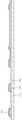
도 1은 본 발명에 따른 조명장치용 OLED 패널의 평면도를 개략적으로 나타낸 것이다.
도 2는 도 1의 I-I' 단면도를 나타낸 예이다.
도 3은 도 1의 II-II' 단면도를 나타낸 예이다.
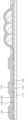
도 4는 도 1의 A 영역의 패시베이션층의 배치 예를 나타낸 단면도이다.
도 3은 도 1의 A 영역의 패시베이션층의 다른 배치 예를 나타낸 단면도이다.
도 6a 내지 도 6k는 본 발명에 따른 조명장치용 OLED 패널을 제조하는 방법을 나타낸 것이다.
1 is a schematic plan view of an OLED panel for a lighting device according to the present invention.
FIG. 2 is an example of a cross-sectional view II′ of FIG. 1 .
FIG. 3 is an example of a II-II' cross-sectional view of FIG. 1 .
FIG. 4 is a cross-sectional view illustrating an arrangement example of a passivation layer in area A of FIG. 1 .
FIG. 3 is a cross-sectional view showing another arrangement example of a passivation layer in region A of FIG. 1 .
6a to 6k show a method of manufacturing an OLED panel for a lighting device according to the present invention.
이하, 도면을 참조하여 본 발명에 따른 조명장치용 OLED 패널 및 그 제조 방법에 대한 실시예를 설명한다.Hereinafter, an embodiment of an OLED panel for a lighting device and a manufacturing method thereof according to the present invention will be described with reference to the drawings.
이하에서 제1, 제2 등과 같이 서수를 포함하는 용어는 다양한 구성요소들을 설명하는데 사용될 수 있지만, 해당 구성요소들은 이와 같은 용어들에 의해 한정되지는 않는다. 이 용어들은 하나의 구성요소들을 다른 구성요소로부터 구별하는 목적으로만 사용된다.Hereinafter, terms including ordinal numbers, such as first and second, may be used to describe various elements, but the elements are not limited by these terms. These terms are only used to distinguish one component from another.
또한, 본 발명에서 “~~ 상에 있다”라고 함은 “어떠한 부분이 다른 부분과 접촉한 상태로 바로 위에 있다”를 의미할 뿐만 아니라 “어떠한 부분이 다른 부분과 비접촉한 상태이거나 제3의 부분이 중간에 더 형성되어 있는 상태로 다른 부분의 위에 있다”를 의미할 수도 있다.In addition, in the present invention, “on” means not only “a part is in contact with another part and is directly above”, but also “a part is not in contact with another part or a third part It can also mean “it is on top of other parts in a state that is more formed in the middle.”
도 1은 본 발명에 따른 조명장치용 OLED 패널의 평면도를 개략적으로 나타낸 것이다. 또한, 도 2는 도 1의 I-I'단면도를 나타낸 예이고, 도 3은 도 1의 II-II' 단면도를 나타낸 예이다.1 is a schematic plan view of an OLED panel for a lighting device according to the present invention. In addition, FIG. 2 is an example showing the II' cross-sectional view of FIG. 1, and FIG. 3 is an example showing the II-II' cross-sectional view of FIG.
도 1 내지 도 3을 참조하면, 본 발명에 따른 조명장치용 OLED 패널은 기판(110), 보조 배선 패턴(120), 제1 전극(130), 패시베이션층(140), OLED 발광 구조체(150), 제2 전극(160) 및 봉지층(170)을 포함한다.1 to 3, an OLED panel for a lighting device according to the present invention includes a
기판(110)은 발광 영역(LA)과, 상기 발광 영역 외곽의 패드 영역(PA)으로 구분된다.The
기판(110)은 글래스 기판, 고분자 기판이 이용될 수 있다. 기판(110)으로, 고분자 기판이 이용될 경우, 고분자 기판의 플렉서블 특성에 기인하여, 롤-투-롤(Roll-to-Roll) 공정으로 조명장치용 OLED 패널이 제조될 수 있다.The
보조 배선 패턴(120)은 기판(110) 상에 배치된다. 본 발명에서 보조 배선 패턴(120)은 상부로 향할수록 폭이 좁아지는 테이퍼 형상의 단면을 갖는다.The
보조 배선 패턴(120)의 역할을 다음과 같다. 후술하는 제1 전극(130)은 ITO(Indium Tin Oxide), FTO(Fluorine-doped Tin Oxide) 등과 같은 TCO(transparent Conductive Oxide) 재질로 형성될 수 있는데, TCO 재질의 경우, OLED 발광 구조체(150)에서 발광되는 광을 투과한다는 장점을 가지지만, 금속에 비해 전기저항이 매우 높다는 단점이 있다. 따라서, 대면적의 조명장치용 OLED 패널을 제조하는 경우, TCO의 높은 저항으로 인해 인가되는 전압의 분포가 제1 전극 전체에 걸쳐 고르지 않게 되며, 이러한 불균일한 전압분포는 대면적 조명장치의 휘도 균일성을 저하시킨다.The role of the
이에, 보조 배선 패턴(120)은 TCO보다 낮은 저항을 갖는 재질, 예를 들어 금속을 포함하는 재질로 형성되어, 보조 배선 패턴(120)과 접촉하여 형성되는 제1 전극(130)에 인가되는 전압의 분포가 제1 전극(130) 전체에 걸쳐 고르게 하는 역할을 한다.Accordingly, the
한편, 보조 배선 패턴(120)은 도 1에 도시된 예와 같은 망 형태가 될 수 있으나, 반드시 이에 제한되는 것은 아니다. 또한, 보조 배선 패턴(120)은 좌우 대칭에 가까운 형태로 형성될 수 있으나, 반드시 이에 제한되는 것은 아니다.Meanwhile, the
제1 전극(130)은 보조 배선 패턴(120)이 배치된 기판 상에 배치된다. 전술한 바와 같이 제1 전극(130)은 ITO와 같은 TCO 재질로 형성될 수 있으며, 스퍼터링 공정 또는 코팅 공정을 통하여 형성될 수 있다.The
패시베이션층(140)은 제1 전극(130) 상에 배치되되, 보조 배선 패턴(120)이 배치된 영역 상에 배치된다.The
OLED 조명에서 제1 전극과 제2 전극 간에 쇼트(short) 발생시, 전류 드롭(current drop)으로 인해 쇼트가 발생된 부분 뿐만 아니라 전체 패널의 휘도 저하가 발생하는 문제점이 있다. 이를 방지하기 위해, 보조배선 패턴(120) 상부에는 패시베이션층(140)이 형성된다.In OLED lighting, when a short occurs between the first electrode and the second electrode, there is a problem in that the luminance of the entire panel as well as the portion where the short occurs is reduced due to a current drop. To prevent this, a
패시베이션층(140)은 폴리이미드계 물질과 같은 유기물 재질로 형성될 수 있고, 알루미나(Al2O3), 질화실리콘(SiNx) 등과 같은 무기물 재질로 형성될 수 있다.The
도 4는 도 1의 A 영역, 즉 발광 영역의 패시베이션층의 배치 예를 나타낸 단면도이다. 도 5는 도 1의 A 영역, 즉 발광 영역의 패시베이션층의 다른 배치 예를 나타낸 단면도이다.FIG. 4 is a cross-sectional view showing an example of arrangement of a passivation layer in area A of FIG. 1, that is, a light emitting area. FIG. 5 is a cross-sectional view showing another arrangement example of a passivation layer in area A of FIG. 1, that is, a light emitting area.
패시베이션층은 도 4에 도시된 예와 같은 단면 형상을 가정할 수 있다. 이는 패시베이션 물질의 증착 및 건식 식각을 통한 패터닝의 결과로 볼 수 있다. 건식 식각을 통항 패터닝시 공정 마진으로 인해 상부 평면부(124a), 경사부(140b) 이외에 하부 평면부(140c)까지 형성된다. 이러한 하부 평면부(140c)의 존재는 발광 면적의 감소를 가져온다. 또한, 건식 식각을 통한 패터닝의 경우 제1 전극(130)도 일부 소실되는 결과를 가져온다. 이는 제1 전극(130)의 두께 균일도를 저하시키는 요인이 될 수 있다.The passivation layer may assume a cross-sectional shape as shown in FIG. 4 . This can be seen as a result of patterning through deposition of a passivation material and dry etching. During patterning through dry etching, the lower
그러나, 도 5에 도시된 예와 같은 단면 형상의 패시베이션층은 보조 배선 패턴(120)에 대응하는 단면 형상을 가질 수 있는데, 보다 구체적으로는 상부 평면부(140a)와, 상부 평면부(140a)로부터 하측방으로 연장되는 경사부(140b)로 이루어지며, 하부 평면부(140c)는 존재하지 않을 수 있다.However, the passivation layer having a cross-sectional shape as shown in FIG. 5 may have a cross-sectional shape corresponding to the
이러한 보조 배선 패턴(120)에 대응하는, 즉 상부 평면부(140a)와 경사부(140b)로 이루어지는 패시베이션층(140)은 후술하는 광분해 가능한 고분자 마스크를 적용함으로써 달성 가능하다. 이 경우, 도 4와는 달리 하부 평면부(140c)가 존재하지 않으며 그만큼 발광면적을 증대시킬 수 있다. 또한, 본 발명에 적용되는 고분자 마스크의 경우 광분해가 가능하여, 제1 전극(130)의 두께 균일도 저하가 문제되지 않는다.The
패시베이션층(140)은 발광 영역(LA)의 가장자리 및 패드 영역(PA)의 가장자리에 추가로 배치되어 있을 수 있다. 발광 영역의 가장자리 및 패드 영역의 가장자리의 경우, 수분 침투에 상대적으로 취약한 영역에 해당한다. 이에 발광 영역의 가장자리 및 패드 영역의 가장자리에 패시베이션을 추가 배치하여 수분 침투에 의한 제1 전극과 제2 전극 간의 쇼트 발생을 방지하는 효과를 높일 수 있다.The
OLED 발광 구조체(150)는 패시베이션층(140)이 배치된 제1 전극(130) 상에 배치된다. OLED 발광 구조체(150)에는 유기 발광층(EML: emission layer)과, 상기 유기 발광층에 홀(hole)을 제공하기 위한, 홀 주입층(HIL: hole injection layer) 및/또는 홀 수송층(HTL: hole transport layer), 상기 유기 발광층에 전자(electron)을 제공하기 위한 전자 수송층(ETL: electron transport layer) 및/또는 전자 주입층(EIL: electron injection layer)가 포함될 수 있다.The OLED
제2 전극(160)은 OLED 발광 구조체(150) 상에 배치된다. 제2 전극(160)은 ITO와 같은 TCO 재질, Al, Ag 등과 같은 금속 재질 등으로 형성될 수 있다. 예를 들어, 하면 발광형일 경우, 제2 전극은 금속 재질일 수 있고, 양면 발광형일 경우, 제2 전극은 TCO 재질일 수 있다.The
한편, OLED 발광 구조체(150) 및 제2 전극(160)은 발광 영역(LA)에 전체적으로 형성될 수 있는 바, 제1 전극(130)의 단면에 대응하는 단면을 가질 수 있다.Meanwhile, the OLED
봉지층(170)은 제2 전극(160) 상에 배치되며, 외부로부터 수분이나 공기가 침부하는 것을 방지하는 역할을 한다. 이러한 봉지층(170)은 아크릴레이트계 화합물, 에폭시계 화합물과 같은 유기물 재질, 세라믹, 금속과 같은 무기물 재질 또는 유무기 복합재로 형성될 수 있으며, 단층 구조 혹은 다층 구조로 형성될 수 있다.The
도 2 및 도 3에는 봉지층(170)이 제2 전극(160)의 상부에만 형성된 예를 나타내었으나, 수분 등의 침투 방지 효과를 높이기 위해 봉지층(170)은 발광 영역에 형성된 각 요소(110~160)의 측면에도 형성될 수 있다.2 and 3 show an example in which the
봉지층(170) 상에는 접착층(180)을 통하여 추가로 보호 필름(190)이 배치될 수 있으며, 이 보호 필름(190) 역시 외부로부터 수분이나 공기가 침투하는 것을 방지하는 역할을 한다. 보호 필름(190)은 PET 기판, 금속 포일 등이 될 수 있다.A
다음으로, 패드 영역(PA)에 대하여 설명하기로 한다. 패드 영역에는 제1 전극 패드(130a) 및 제2 전극 패드(160a)가 배치된다. 제1 전극 패드(130a) 및 제2 전극 패드(160a)는 외부 전원에 연결된다. 제1 전극 패드(130a)는 제1 전극(130)과 연결된다. 그리고, 제2 전극 패드(160a)는 제2 전극(160)과 연결된다. 도 1에는 패드 영역의 중앙부에 제2 전극 패드(160a)가 배치되어 있고, 제2 전극 패드(160a) 양측에 제1 전극 패드들(130a)이 배치되어 있는 예를 나타내었으나, 제1 전극 패드(130a)가 제1 전극(130)과 전기적으로 연결되고, 제2 전극 패드(160a)가 제2 전극(160)과 전기적으로 연결된다면, 전극 패드의 배치 형태나, 전극 패드의 크기, 전극 패드의 개수 등은 필요에 따라 변경 가능하다.Next, the pad area PA will be described. A
도 2를 참조하면, 제1 전극 패드(130a)는 보조 배선 패턴(120)과 동일한 재질의 하부층(131)과 제1 전극(130)과 동일한 재질의 상부층(132)을 포함할 수 있다. 하부층(131)은 보조 배선 패턴(120)과 동시에 형성될 수 있으며, 보조 배선 패턴(120)과 직접 연결될 수도 있다. 상부층(132)은 제1 전극(130)과 동시에 형성될 수 있다. 하부층(131)이 보조 배선 패턴(120)과 직접 연결되는 경우, 상부층(132)은 제1 전극(130)과 직접 연결되지 않아도 된다.Referring to FIG. 2 , the
또한, 도 3을 참조하면, 제2 전극 패드(160a)는 보조 배선 패턴(120)과 동일한 재질의 하부층(161)과 제2 전극(160)과 동일한 재질의 상부층(162)을 포함할 수 있다. 하부층(161)은 보조 배선 패턴(120)과 동시에 형성될 수 있으며, 상부층(162)은 제2 전극(160)과 동시에 형성될 수 있다.Also, referring to FIG. 3 , the
이하, 도 6a 내지 도 6k를 참조하여 본 발명에 따른 조명장치용 OLED를 제조하는 방법에 대하여 설명하기로 한다.Hereinafter, a method of manufacturing an OLED for a lighting device according to the present invention will be described with reference to FIGS. 6A to 6K.
우선, 도 6a에 도시된 예와 같이, 발광 영역(LA)과, 발광 영역(LA) 외곽의 패드 영역으로 구분되는 기판(110) 상에 보조 배선 패턴(120)을 배치한다.First, as in the example shown in FIG. 6A , an
보조 배선 패턴(120)은 금속 재질로 형성될 수 있고, 증착 및 건식 식각을 통하여 상부로 향할수록 폭이 좁아지는 테이퍼 형태의 단면을 가질 수 있다.The
또한, 보조 배선 패턴(120)은 발광 영역(LA) 및 패드 영역(PA) 모두에 형성될 수 있다. 패드 영역(PA)에 관하여, 본 단계에서 보조 배선 패턴과 동일한 재질의 제1 전극 패턴의 하부층(도 2의 131) 및 제2 전극 패턴의 하부층(도 3의 161)을 형성할 수 있다.In addition, the
다음으로, 도 6b에 도시된 예와 같이, 보조 배선 패턴(120)이 배치된 기판 상에 제1 전극(130)을 배치한다. 제1 전극(130)은 ITO와 같은 투명전도성산화물(TCO) 재질로 형성될 수 있다. 제1 전극(130)은 발광 영역(LA) 전체에 형성될 수 있고, 제1 전극 패드(130a)를 형성하기 위해 패드 영역(PA)의 일부에도 형성된다. 즉, 제1 전극 배치 단계에서 제1 전극과 동일한 재질의 제1 전극 패드의 상부층(132)을 형성한다.Next, as in the example shown in FIG. 6B , the
다음으로, 도 6c 내지 도 6e에 도시된 예와 같이 패시베이션층(140)을 형성한다.Next, a
우선, 도 6c에 도시된 예와 같이, 제1 전극(130) 상에 고분자(135)를 배치하되 발광 영역의 보조 배선 패턴들 사이에 고분자를 배치한다.First, as in the example shown in FIG. 6C, a
고분자(135)의 배치는 잉크젯 인쇄법으로 액상 고분자를 원하는 영역에 인쇄한 후, 경화 공정을 통하여 이루어질 수 있다. 액상 고분자는 고분자가 용매에 용해되어 있는 상태 혹은 해당 공정 온도에서 액상 상태인 고분자를 의미한다. 액상 고분자로는 저온 경화가 가능한 PVA(poly-vinvl alchohol), PMMA(Poly-methyl methacrylate) 등이 이용될 수 있으나, 이에 제한되는 것은 아니다.Disposition of the
본 발명의 경우, 보조 전극(120)이 단차로 작용하고, 이 단차에 의해, 잉크젯 인쇄된 고분자가 보조 배선 패턴들 사이에 자가 정렬(self alignment)될 수 있다. 잉크젯 인쇄된 고분자는 표면 장력에 의해 도시된 바와 같이 반구형 형태를 가질 수 있다.In the case of the present invention, the
또한, 패드 영역(PA)의 제1 전극 패드 상에도 고분자가 배치될 수 있는데, 이는 패드 영역 가장자리에도 패시베이션층을 형성하기 위함이다.In addition, a polymer may also be disposed on the first electrode pad of the pad area PA, which is to form a passivation layer also at the edge of the pad area.
한편, 수분이나 공기 침투에 취약한 발광 영역(LA)의 가장자리 및 패드 영역(PA)의 가장자리에 패시베이션층(140)이 추가로 배치되도록 할 필요가 있다. 이를 위해, 발광 영역(LA)의 가장자리 및 패드 영역(PA)의 가장자리에는 고분자를 배치하지 않을 수 있다.Meanwhile, the
이후, 도 6d에 도시된 예와 같이, 고분자(135)를 마스크로 하여, 제1 전극(130) 상에 패시베이션 물질을 증착한다.Then, as in the example shown in FIG. 6D , a passivation material is deposited on the
패시베이션 물질은 폴리이미드 등과 같은 유기물, 알루미나, 질화실리콘과 같은 무기물이 될 수 있다. 패시베이션 물질의 증착은 원자층 증착(ALD) 방법, 화학기상증착(CVD) 방법 등이 이용될 수 있고, 보다 바람직하게는 상압 ALD 증착 방법을 제시할 수 있다. 상압 ALD 방법은 상압에서 원자단위로 박막을 형성하는 증착법으로서, 표면 반응(Surface Reaction) 및 부산물의 탈착(Desorption)을 기초로 한다. 주로, TMA(trimethly-aluminium)을 전구체로 하여 Al2O3을 ALD(atomic layer deposition)방법으로 증착한다. 이에 한정되지 않고, 전구체를 Zr(NMe2)4, HfCl4, TiCl4등으로 하여, Al2O3, ZrO2, HfO2, TiO2등을 상압 ALD 방법으로 증착할 수 있다.The passivation material may be an organic material such as polyimide or an inorganic material such as alumina or silicon nitride. For the deposition of the passivation material, an atomic layer deposition (ALD) method, a chemical vapor deposition (CVD) method, or the like may be used, and more preferably, an atmospheric pressure ALD deposition method may be suggested. The atmospheric pressure ALD method is a deposition method for forming a thin film in atomic units at atmospheric pressure, and is based on surface reaction and desorption of by-products. Mainly, using TMA (trimethly-aluminium) as a precursor, Al2 O3 is deposited by ALD (atomic layer deposition) method. It is not limited thereto, and Al2 O3 , ZrO2 , HfO 2 , TiO2 , etc. may be deposited by atmospheric pressure ALD using Zr(NMe2 )4 , HfCl4, TiCl4 , or the like as a precursor.
이후, 도 6e에 도시된 예와 같이, 고분자(135)를 제거하여 발광 영역(LA)의 보조 배선 패턴들 상부 영역에 패시베이션층을 형성한다. 또한, 도 6e에 도시된 예와 같이 본 단계에서 패드 영역에 형성된 고분자도 함께 제거할 수 있다. 다른 예로, 도 6f에 도시된 예와 같이 패드 영역에 형성된 고분자를 잔류시킬 수 있고, 후속 공정(예를 들어 도 6j의 패드 오픈 단계)에서 제거할 수 있다.Then, as shown in FIG. 6E , the
한편, 고분자에는 광분해 가능한 촉매가 포함되고, 고분자의 제거는 광 조사에 의해 촉매를 광분해시키는 방법으로 수행될 수 있다. 이러한 광분해 가능한 촉매는 TiO2, ZnO, CDS, ZrO2, SnO2, V2O2. WO3, Cerium stearate, SrTiO3 등이 이용될 수 있다. 고분자 제거를 위해 이용되는 광은 레이저 광이 될 수 있고, 펄스 형태로 주기적으로 광을 조사하는 IPL(Intense Pulsed Light)이 이용될 수 있다. IPL 형태의 광을 이용할 경우, 기판의 온도가 일정하게 유지된 상태에서, 광분해 가능한 촉매가 활성화되어, 고분자의 점착력을 약화시킬 수 있다.Meanwhile, the polymer includes a catalyst capable of photodegradation, and removal of the polymer may be performed by photodegrading the catalyst by light irradiation. These photodegradable catalysts are TiO2 , ZnO, CDS, ZrO2 , SnO2 , V2 O2 . WO3 , Cerium stearate, SrTiO3 and the like may be used. The light used to remove the polymer may be laser light, or IPL (Intense Pulsed Light) that periodically irradiates light in a pulse form may be used. In the case of using IPL type light, a catalyst capable of photolysis is activated while the temperature of the substrate is kept constant, thereby weakening the adhesive force of the polymer.
다음으로, 도 6g에 도시된 예와 같이, 발광 영역(LA)에 OLED 발광 구조체(150)를 배치한다. OLED 발광 구조체(150)의 각 층은 예를 들어, 구리 프탈로시아닌(CuPc: copperphthalocyanine), N,N-디(나프탈렌-1-일)-N, N'-디페닐-벤지딘(N,N'-Di(naphthalene-1-yl)-N,N'-diphenylbenzidine: NPB), 트리스-8-하이드록시퀴놀린 알루미늄(tris-8-hydroxyquinoline aluminum)(Alq3) 등의 유기물을 진공 증착법으로 증착하는 방법을 이용하여 형성할 수 있다.Next, as in the example shown in FIG. 6G , the OLED
다음으로, 도 6h에 도시된 예와 같이, OLED 발광 구조체(150) 상에 제2 전극(160)을 배치한다. 제2 전극(160)은 금속이나 TCO 재질로 형성될 수 있다.Next, as in the example shown in FIG. 6H , the
제2 전극(160)은 발광 영역에 전체적으로 형성되고, 도 3에 도시된 예와 같이, 제2 전극 패드(160a)를 형성하기 위해 패드 영역(PA)의 일부에도 형성된다. 제2 전극 배치 단계에서, 제2 전극과 동일한 재질의 제2 전극 패드의 상부층(162)을 형성할 수 있다.The
제2 전극(160) 형성 후, 필요에 따라서는 유기층(135)에 에이징 전압을 인가하여 OLED 발광 구조체(150)를 에이징하는 과정을 더 수행할 수 있다. 유기발광물질은 수명이 짧고, 수분이나 산소에 취약하며 고전압이나 고전류의 인가 시에 소자의 손상이 발생할 수 있다. 또한, 제1 및 제2 전극(130, 160)과 OLED 발광 구조체(150) 사이의 계면특성이 좋지 않으므로 소자의 특성이 불안정한 문제점도 있다. 또한, 제2 전극(160)의 형성시 OLED 발광 구조체(150) 내에 불순물이 적층되어 유기물의 발광특성 및 색감을 저하시킬 수도 있다.After forming the
이러한 문제를 해결하기 위해, OLED 발광 구조체(150)에 고전압의 에이징 전압을 인가하여 OLED 발광 구조체(150)를 단시간에 에이징(aging)할 수 있다. 이때, 에이징 전압은 제1 전극(130) 및 제2 전극(160)에 인가되는 전압보다 큰 고전압일 수 있으며, 제1 전극(130) 및 제2 전극(160)에 인가되는 전압의 역전압일 수 있다.In order to solve this problem, the OLED
다음으로, 도 6i에 도시된 예와 같이, 제2 전극(160) 상에 봉지층(170)을 형성한다.Next, as in the example shown in FIG. 6i , an
또한, 제1 전극 패드(130a) 상에 고분자(135)가 잔류하고 있을 경우, 패드 오픈을 위해 도 6j에 도시된 예와 같이 고분자(135)를 제거하는 공정을 수행한다.In addition, when the
또한, 도 6k와 같이 평탄화된 접착층(180)을 배치하고, 그 위에 보호 필름(190)을 부착하는 공정을 더 수행할 수 있다. 보호 필름(190)은 외부로부터 수분이나 공기가 침투하는 것을 방지하는 역할을 하며, PET 기판, 금속 포일 등이 이용될 수 있다.In addition, as shown in FIG. 6K , a process of disposing the flattened
이상의 과정을 통하여 본 발명에 따른 조명장치용 OLED 패널이 제조될 수 있으며, 상기의 공정들 이외에 공지된 추가의 공정이 더 포함될 수 있다.An OLED panel for a lighting device according to the present invention may be manufactured through the above process, and additional known processes may be further included in addition to the above processes.
이상에서는 본 발명의 실시예를 중심으로 설명하였지만, 통상의 기술자의 수준에서 다양한 변경이나 변형을 가할 수 있다. 따라서, 이러한 변경과 변형이 본 발명의 범위를 벗어나지 않는 한 본 발명의 범주 내에 포함되는 것으로 이해할 수 있을 것이다.Although the above has been described based on the embodiments of the present invention, various changes or modifications may be made at the level of those skilled in the art. Accordingly, it will be understood that such changes and modifications are included within the scope of the present invention as long as they do not depart from the scope of the present invention.
LA : 발광 영역
PA : 패드 영역
110 : 기판
120 : 보조 배선 패턴
130 : 제1 전극
130a : 제1 전극 패드
131 : 제1 전극 패드의 하부층
132 : 제1 전극 패드의 상부층
135 : 고분자
140 : 패시베이션층
150 : OLED 구조체
160 : 제2 전극
160a : 제2 전극 패드
161 : 제1 전극 패드의 하부층
162 : 제1 전극 패드의 상부층
170 : 봉지층
180 : 접착제층
190 : 보호필름LA: luminous area
PA: pad area
110: substrate
120: auxiliary wiring pattern
130: first electrode
130a: first electrode pad
131: lower layer of the first electrode pad
132: upper layer of the first electrode pad
135: polymer
140: passivation layer
150: OLED structure
160: second electrode
160a: second electrode pad
161: lower layer of the first electrode pad
162: upper layer of the first electrode pad
170: encapsulation layer
180: adhesive layer
190: protective film
Claims (14)
Translated fromKorean상기 기판 상에 배치되며, 상부로 향할수록 폭이 좁아지는 테이퍼 형상의 단면을 갖는 보조 배선 패턴;
상기 보조 배선 패턴 및 상기 기판 상에 배치되는 제1 전극;
상기 제1 전극 상에 배치되며, 상기 보조 배선 패턴과 중첩하도록 배치되는 패시베이션층;
상기 발광 영역에서 상기 패시베이션층 및 상기 제1 전극 상에 배치되는 OLED 발광 구조체;
상기 OLED 발광 구조체 상에 배치되는 제2 전극; 및
상기 제2 전극 상에 배치되는 봉지층을 포함하고,
상기 발광 영역에서, 상기 패시베이션층은 상기 보조 배선 패턴의 단면에 대응하는 단면을 갖고,
상기 발광 영역에서, 상기 패시베이션층은 상기 보조 배선 패턴이 배치된 영역에 위치하고,
상기 발광 영역의 가장자리 및 상기 패드 영역의 가장자리를 덮도록 상기 패시베이션층이 배치되고,
상기 패드 영역의 가장자리는 상기 패드 영역과 상기 발광 영역 사이의 경계에 대응한 일부와 상기 기판의 가장자리에 대응한 다른 일부를 포함하고,
상기 패드 영역에, 상기 제1 전극과 연결되는 제1 전극 패드 및 상기 제2 전극과 연결되는 제2 전극 패드가 배치되어 있되,
상기 제1 전극 패드는 상기 보조 배선 패턴과 동일한 재질의 하부층과 상기 제1 전극과 동일한 재질의 상부층을 포함하고,
상기 제2 전극 패드는 상기 보조 배선 패턴과 동일한 재질의 하부층과 상기 제2 전극과 동일한 재질의 상부층을 포함하고,
상기 패드 영역에서, 상기 패시베이션층은 상기 제1 전극 패드의 상기 상부층의 가장 자리를 덮으며,
상기 패드 영역에서, 상기 패시베이션층은 상기 제2 전극 패드의 상기 하부층과 상기 상부층 사이에 배치되고, 상기 제2 전극 패드의 상기 하부층의 가장 자리를 덮는, 조명장치용 OLED 패널.
a substrate divided into a light emitting area and a pad area outside the light emitting area;
an auxiliary wiring pattern disposed on the substrate and having a tapered cross-section with a width narrowing toward the top;
a first electrode disposed on the auxiliary wiring pattern and the substrate;
a passivation layer disposed on the first electrode and overlapping the auxiliary wiring pattern;
an OLED light emitting structure disposed on the passivation layer and the first electrode in the light emitting region;
a second electrode disposed on the OLED light emitting structure; and
Including an encapsulation layer disposed on the second electrode,
In the light emitting region, the passivation layer has a cross section corresponding to the cross section of the auxiliary wiring pattern,
In the light emitting region, the passivation layer is located in a region where the auxiliary wiring pattern is disposed;
The passivation layer is disposed to cover an edge of the light emitting region and an edge of the pad region,
The edge of the pad area includes a part corresponding to the boundary between the pad area and the light emitting area and another part corresponding to the edge of the substrate;
In the pad area, a first electrode pad connected to the first electrode and a second electrode pad connected to the second electrode are disposed,
The first electrode pad includes a lower layer made of the same material as the auxiliary wiring pattern and an upper layer made of the same material as the first electrode,
The second electrode pad includes a lower layer made of the same material as the auxiliary wiring pattern and an upper layer made of the same material as the second electrode,
In the pad region, the passivation layer covers an edge of the upper layer of the first electrode pad,
In the pad region, the passivation layer is disposed between the lower layer and the upper layer of the second electrode pad, and covers an edge of the lower layer of the second electrode pad.
상기 패시베이션층은 상부 평면부와, 상기 상부 평면부로부터 하측방으로 연장되는 경사부로 이루어지는 단면을 갖는, 조명장치용 OLED 패널.
According to claim 1,
The passivation layer has a cross section composed of an upper flat portion and an inclined portion extending downward from the upper flat portion, OLED panel for a lighting device.
상기 제1 전극은 TCO(Transparent Conductive Oxide) 재질이고,
상기 보조 배선 패턴은 금속을 포함하는 재질인, 조명장치용 OLED 패널.
According to claim 1,
The first electrode is a TCO (Transparent Conductive Oxide) material,
The auxiliary wiring pattern is a material containing metal, an OLED panel for a lighting device.
상기 OLED 발광 구조체 및 상기 제2 전극은 상기 제1 전극의 단면에 대응하는 단면을 갖는, 조명장치용 OLED 패널.
According to claim 1,
The OLED light emitting structure and the second electrode have a cross section corresponding to the cross section of the first electrode, an OLED panel for a lighting device.
상기 보조 배선 패턴 및 상기 기판 상에 제1 전극을 배치하는 단계;
상기 제1 전극 상에 고분자를 배치하되 상기 발광 영역의 상기 보조 배선 패턴들 사이에 고분자를 배치하는 단계;
상기 고분자를 마스크로 하여, 상기 제1 전극 상에 패시베이션 물질을 증착한 후, 상기 고분자를 제거하여 상기 발광 영역의 상기 보조 배선 패턴들의 상부 영역에 패시베이션층을 형성하는 단계;
상기 발광 영역에서 상기 패시베이션층 및 상기 제1 전극 상에 OLED 발광 구조체를 배치하는 단계;
상기 OLED 발광 구조체 상에 제2 전극을 배치하는 단계; 및
상기 제2 전극 상에 봉지층을 형성하는 단계를 포함하고,
상기 발광 영역의 가장자리 및 상기 패드 영역의 가장자리를 덮도록 상기 패시베이션층이 배치되고,
상기 발광 영역에서, 상기 보조 배선 패턴과 중첩하지 않는 영역에 상기 고분자를 형성하고, 상기 발광 영역의 가장자리 및 상기 패드 영역의 가장자리에는 상기 고분자를 형성하지 않으며,
상기 패드 영역의 가장자리는 상기 패드 영역과 상기 발광 영역 사이의 경계에 대응한 일부와 상기 기판의 가장자리에 대응한 다른 일부를 포함하고,
상기 고분자에 촉매가 포함되어 있는, 조명장치용 OLED 패널 제조 방법.
disposing auxiliary wiring patterns on the light emitting area and the pad area of the substrate divided into a light emitting area and a pad area outside the light emitting area;
disposing a first electrode on the auxiliary wiring pattern and the substrate;
disposing a polymer on the first electrode and disposing the polymer between the auxiliary wiring patterns of the light emitting region;
depositing a passivation material on the first electrode using the polymer as a mask, and then removing the polymer to form a passivation layer in an upper region of the auxiliary wiring patterns in the light emitting region;
disposing an OLED light emitting structure on the passivation layer and the first electrode in the light emitting region;
disposing a second electrode on the OLED light emitting structure; and
Forming an encapsulation layer on the second electrode,
The passivation layer is disposed to cover an edge of the light emitting region and an edge of the pad region,
In the light emitting region, the polymer is formed in a region that does not overlap with the auxiliary wiring pattern, and the polymer is not formed at an edge of the light emitting region and an edge of the pad region;
The edge of the pad area includes a part corresponding to the boundary between the pad area and the light emitting area and another part corresponding to the edge of the substrate;
Method for manufacturing an OLED panel for a lighting device, wherein the polymer contains a catalyst.
상기 고분자의 배치는 잉크젯법에 의해 액상 고분자를 인쇄한 후, 경화하는 방법으로 수행되는, 조명장치용 OLED 패널 제조 방법.
According to claim 6,
The arrangement of the polymer is performed by a method of curing after printing a liquid polymer by an inkjet method, a method for manufacturing an OLED panel for a lighting device.
상기 패시베이션 물질의 증착은 상압 ALD 증착 방법으로 수행되는, 조명장치용 OLED 패널 제조 방법.
According to claim 6,
Deposition of the passivation material is carried out by atmospheric pressure ALD deposition method, OLED panel manufacturing method for a lighting device.
상기 고분자의 제거는 광 조사에 의해 상기 촉매를 활성화시켜 상기 고분자의 점착력을 완화시키는 방법으로 수행되는, 조명장치용 OLED 패널 제조 방법.
According to claim 6,
Removal of the polymer is performed by activating the catalyst by light irradiation to relieve the adhesive force of the polymer, OLED panel manufacturing method for a lighting device.
상기 촉매는 TiO2, ZnO, CDS, ZrO2, SnO2, V2O2. WO3, Cerium stearate, SrTiO3 중 적어도 하나를 포함하는, 조명장치용 OLED 패널 제조 방법.
According to claim 9,
The catalyst is TiO2 , ZnO, CDS, ZrO2 , SnO2 , V2 O2 . WO3 , Cerium stearate, SrTiO3 A method of manufacturing an OLED panel for a lighting device comprising at least one of.
상기 패드 영역에, 상기 제1 전극과 연결되는 제1 전극 패드 및 상기 제2 전극과 연결되는 제2 전극 패드를 배치하되,
상기 보조 배선 패턴 배치 단계에서 상기 보조 배선 패턴과 동일한 재질의 하부층을 배치하고, 상기 제1 전극 배치 단계에서 상기 제1 전극과 동일한 재질의 상부층을 배치하는 방법으로 상기 제1 전극 패드를 배치하고,
상기 보조 배선 패턴 배치 단계에서 상기 보조 배선 패턴과 동일한 재질의 하부층을 배치하고, 상기 제2 전극 배치 단계에서 상기 제2 전극과 동일한 재질의 상부층을 배치하는 방법으로 상기 제2 전극 패드를 배치하는, 조명장치용 OLED 패널 제조 방법.
According to claim 6,
Disposing a first electrode pad connected to the first electrode and a second electrode pad connected to the second electrode in the pad area,
In the auxiliary wiring pattern arranging step, a lower layer made of the same material as the auxiliary wiring pattern is disposed, and in the first electrode arranging step, the first electrode pad is disposed by disposing an upper layer made of the same material as the first electrode,
Disposing the second electrode pad by disposing a lower layer of the same material as the auxiliary wiring pattern in the auxiliary wiring pattern arranging step, and disposing an upper layer of the same material as the second electrode in the second electrode arranging step, OLED panel manufacturing method for lighting device.
상기 제1 전극 패드의 상부층 상에 고분자를 추가로 배치하고, 상기 고분자 제거 시에 상기 제1 전극 패드의 상부층 상에 배치된 고분자를 함께 제거하여 상기 제1 전극 패드의 상부층을 노출시키는, 조명장치용 OLED 패널 제조 방법.
According to claim 11,
A lighting device in which a polymer is additionally disposed on the upper layer of the first electrode pad, and when the polymer is removed, the polymer disposed on the upper layer of the first electrode pad is removed together to expose the upper layer of the first electrode pad. A method for manufacturing an OLED panel for use.
상기 제1 전극 패드의 상부층 상에 고분자를 추가로 배치하고, 상기 봉지층 형성 후에 상기 제1 전극 패드의 상부층 상에 배치된 고분자를 제거하여 제1 전극 패드의 상부층을 노출시키는, 조명장치용 OLED 패널 제조 방법.According to claim 11,
An OLED for a lighting device in which a polymer is additionally disposed on the upper layer of the first electrode pad and the upper layer of the first electrode pad is exposed by removing the polymer disposed on the upper layer of the first electrode pad after forming the encapsulation layer. How to make a panel.
Priority Applications (6)
| Application Number | Priority Date | Filing Date | Title |
|---|---|---|---|
| KR1020170162293AKR102516699B1 (en) | 2017-11-29 | 2017-11-29 | Oled panel for lighting device and method of manufacturing the same |
| US16/184,671US10608074B2 (en) | 2017-11-29 | 2018-11-08 | OLED panel for lighting device and method of manufacturing the same |
| DE102018128167.6ADE102018128167B4 (en) | 2017-11-29 | 2018-11-12 | OLED panel for lighting device and method for manufacturing the same |
| CN201811384699.0ACN110010640B (en) | 2017-11-29 | 2018-11-20 | OLED panel for lighting device and manufacturing method thereof |
| JP2018217995AJP6786574B2 (en) | 2017-11-29 | 2018-11-21 | OLED panel for lighting equipment and its manufacturing method |
| GB1819108.0AGB2569883B (en) | 2017-11-29 | 2018-11-23 | OLED panel for lighting device and method of manufacturing the same |
Applications Claiming Priority (1)
| Application Number | Priority Date | Filing Date | Title |
|---|---|---|---|
| KR1020170162293AKR102516699B1 (en) | 2017-11-29 | 2017-11-29 | Oled panel for lighting device and method of manufacturing the same |
Publications (2)
| Publication Number | Publication Date |
|---|---|
| KR20190063311A KR20190063311A (en) | 2019-06-07 |
| KR102516699B1true KR102516699B1 (en) | 2023-03-30 |
Family
ID=65024509
Family Applications (1)
| Application Number | Title | Priority Date | Filing Date |
|---|---|---|---|
| KR1020170162293AActiveKR102516699B1 (en) | 2017-11-29 | 2017-11-29 | Oled panel for lighting device and method of manufacturing the same |
Country Status (6)
| Country | Link |
|---|---|
| US (1) | US10608074B2 (en) |
| JP (1) | JP6786574B2 (en) |
| KR (1) | KR102516699B1 (en) |
| CN (1) | CN110010640B (en) |
| DE (1) | DE102018128167B4 (en) |
| GB (1) | GB2569883B (en) |
Families Citing this family (2)
| Publication number | Priority date | Publication date | Assignee | Title |
|---|---|---|---|---|
| KR102423121B1 (en)* | 2017-11-29 | 2022-07-19 | 엘지디스플레이 주식회사 | Oled panel for lighting device and method of manufacturing the same |
| CN111048571A (en)* | 2019-12-26 | 2020-04-21 | 安徽熙泰智能科技有限公司 | Preparation method of silicon-based OLED micro-display |
Citations (6)
| Publication number | Priority date | Publication date | Assignee | Title |
|---|---|---|---|---|
| JP2003036971A (en)* | 2001-07-25 | 2003-02-07 | Dainippon Printing Co Ltd | Method of manufacturing electroluminescent device |
| JP2005183209A (en)* | 2003-12-19 | 2005-07-07 | Asahi Glass Co Ltd | Organic EL display device and manufacturing method thereof |
| JP2012049112A (en)* | 2010-07-26 | 2012-03-08 | Semiconductor Energy Lab Co Ltd | Light-emitting device, lighting device, and method of manufacturing light-emitting device |
| WO2014122938A1 (en)* | 2013-02-07 | 2014-08-14 | パナソニック株式会社 | Organic electroluminescence element and illumination device |
| JP2015220089A (en)* | 2014-05-16 | 2015-12-07 | パイオニア株式会社 | Method for manufacturing light-emitting device |
| JP2017143172A (en)* | 2016-02-10 | 2017-08-17 | セイコーエプソン株式会社 | Electro-optical device and electronic apparatus |
Family Cites Families (22)
| Publication number | Priority date | Publication date | Assignee | Title |
|---|---|---|---|---|
| EP1343206B1 (en)* | 2002-03-07 | 2016-10-26 | Semiconductor Energy Laboratory Co., Ltd. | Light emitting apparatus, electronic apparatus, illuminating device and method of fabricating the light emitting apparatus |
| CN1871711B (en)* | 2003-10-28 | 2011-12-07 | 株式会社半导体能源研究所 | Display device, method for manufacturing same, and television receiver |
| JP4770519B2 (en)* | 2006-03-01 | 2011-09-14 | セイコーエプソン株式会社 | ORGANIC LIGHT EMITTING DEVICE, METHOD FOR MANUFACTURING ORGANIC LIGHT EMITTING DEVICE, AND ELECTRONIC DEVICE |
| KR101281918B1 (en)* | 2006-05-17 | 2013-07-03 | 엘지디스플레이 주식회사 | Diode Substrate of Transflective Type And Method for Fabricating The Same |
| JP4752818B2 (en)* | 2007-07-06 | 2011-08-17 | ソニー株式会社 | Organic EL display device, electronic device, substrate for organic EL display device, and method for manufacturing organic EL display device |
| KR101857405B1 (en) | 2009-07-10 | 2018-05-11 | 가부시키가이샤 한도오따이 에네루기 켄큐쇼 | Semiconductor device and method for manufacturing the same |
| JP5685855B2 (en)* | 2009-09-08 | 2015-03-18 | 株式会社リコー | Display device and manufacturing method of display device |
| KR101094300B1 (en) | 2009-10-12 | 2011-12-19 | 삼성모바일디스플레이주식회사 | Organic light-emitting lighting apparatus and method for manufacturing same |
| CN102668706B (en)* | 2009-11-17 | 2015-03-25 | 联合创新技术有限公司 | Organic el display |
| EP2858137B1 (en)* | 2012-05-31 | 2018-08-29 | LG Display Co., Ltd. | Organic light-emitting device |
| DE102013110037B4 (en) | 2013-09-12 | 2018-05-09 | Osram Oled Gmbh | Method for producing an optoelectronic component |
| JP2015227328A (en) | 2014-05-02 | 2015-12-17 | 株式会社半導体エネルギー研究所 | COMPOUND, LIGHT EMITTING ELEMENT, LIGHT EMITTING DEVICE, ELECTRONIC DEVICE, AND LIGHTING DEVICE |
| US9859345B2 (en)* | 2014-09-17 | 2018-01-02 | Lg Display Co., Ltd. | Organic light emitting display device including a partition wall and method of manufacturing the same |
| CN106206656B (en)* | 2015-05-28 | 2019-11-15 | 乐金显示有限公司 | Organic light emitting display device and manufacturing method thereof |
| KR102618599B1 (en)* | 2016-11-30 | 2023-12-27 | 엘지디스플레이 주식회사 | Lighting apparatus using organic light emitting diode and method of fabricating the same |
| KR102712048B1 (en) | 2016-11-30 | 2024-09-27 | 엘지디스플레이 주식회사 | Lighting apparatus using organic light emitting diode and method of fabricating the same |
| KR102652261B1 (en)* | 2016-12-07 | 2024-03-27 | 엘지디스플레이 주식회사 | Lighting apparatus using organic light emitting diode |
| KR102555383B1 (en)* | 2016-12-07 | 2023-07-12 | 엘지디스플레이 주식회사 | Lighting apparatus using organic light emitting diode and method of fabricating the same |
| KR102321663B1 (en)* | 2017-07-11 | 2021-11-03 | 엘지디스플레이 주식회사 | Lighting apparatus using organic light emitting diode and method of fabricating thereof |
| KR102415045B1 (en)* | 2017-11-28 | 2022-06-29 | 엘지디스플레이 주식회사 | Light apparatus for organic light emitting device |
| KR102423121B1 (en)* | 2017-11-29 | 2022-07-19 | 엘지디스플레이 주식회사 | Oled panel for lighting device and method of manufacturing the same |
| KR102452841B1 (en)* | 2017-12-05 | 2022-10-07 | 엘지디스플레이 주식회사 | Flexible oled panel for lighting device and method of manufacturing the same |
- 2017
- 2017-11-29KRKR1020170162293Apatent/KR102516699B1/enactiveActive
- 2018
- 2018-11-08USUS16/184,671patent/US10608074B2/enactiveActive
- 2018-11-12DEDE102018128167.6Apatent/DE102018128167B4/enactiveActive
- 2018-11-20CNCN201811384699.0Apatent/CN110010640B/enactiveActive
- 2018-11-21JPJP2018217995Apatent/JP6786574B2/enactiveActive
- 2018-11-23GBGB1819108.0Apatent/GB2569883B/enactiveActive
Patent Citations (6)
| Publication number | Priority date | Publication date | Assignee | Title |
|---|---|---|---|---|
| JP2003036971A (en)* | 2001-07-25 | 2003-02-07 | Dainippon Printing Co Ltd | Method of manufacturing electroluminescent device |
| JP2005183209A (en)* | 2003-12-19 | 2005-07-07 | Asahi Glass Co Ltd | Organic EL display device and manufacturing method thereof |
| JP2012049112A (en)* | 2010-07-26 | 2012-03-08 | Semiconductor Energy Lab Co Ltd | Light-emitting device, lighting device, and method of manufacturing light-emitting device |
| WO2014122938A1 (en)* | 2013-02-07 | 2014-08-14 | パナソニック株式会社 | Organic electroluminescence element and illumination device |
| JP2015220089A (en)* | 2014-05-16 | 2015-12-07 | パイオニア株式会社 | Method for manufacturing light-emitting device |
| JP2017143172A (en)* | 2016-02-10 | 2017-08-17 | セイコーエプソン株式会社 | Electro-optical device and electronic apparatus |
Also Published As
| Publication number | Publication date |
|---|---|
| CN110010640B (en) | 2023-07-11 |
| JP6786574B2 (en) | 2020-11-18 |
| DE102018128167A1 (en) | 2019-05-29 |
| CN110010640A (en) | 2019-07-12 |
| US10608074B2 (en) | 2020-03-31 |
| GB201819108D0 (en) | 2019-01-09 |
| US20190165086A1 (en) | 2019-05-30 |
| GB2569883B (en) | 2021-06-16 |
| KR20190063311A (en) | 2019-06-07 |
| JP2019102445A (en) | 2019-06-24 |
| GB2569883A (en) | 2019-07-03 |
| DE102018128167B4 (en) | 2024-06-13 |
Similar Documents
| Publication | Publication Date | Title |
|---|---|---|
| US8710522B2 (en) | Organic light emitting diode light source device | |
| CN110021710B (en) | Flexible OLED panel for lighting device and manufacturing method thereof | |
| KR102516699B1 (en) | Oled panel for lighting device and method of manufacturing the same | |
| US20140070173A1 (en) | Cuttable organic light emitting diode light source device with wireless power transmission | |
| JP6751747B2 (en) | OLED panel for lighting equipment and its manufacturing method | |
| CN110034155B (en) | OLED panel for lighting device and manufacturing method thereof | |
| US20230034282A1 (en) | Oled panel for lighting device with moisture intrusion delay effect | |
| US10797262B2 (en) | Organic-based lighting device |
Legal Events
| Date | Code | Title | Description |
|---|---|---|---|
| PA0109 | Patent application | Patent event code:PA01091R01D Comment text:Patent Application Patent event date:20171129 | |
| PG1501 | Laying open of application | ||
| A201 | Request for examination | ||
| PA0201 | Request for examination | Patent event code:PA02012R01D Patent event date:20200928 Comment text:Request for Examination of Application Patent event code:PA02011R01I Patent event date:20171129 Comment text:Patent Application | |
| E902 | Notification of reason for refusal | ||
| PE0902 | Notice of grounds for rejection | Comment text:Notification of reason for refusal Patent event date:20211208 Patent event code:PE09021S01D | |
| E902 | Notification of reason for refusal | ||
| PE0902 | Notice of grounds for rejection | Comment text:Notification of reason for refusal Patent event date:20220629 Patent event code:PE09021S01D | |
| E701 | Decision to grant or registration of patent right | ||
| PE0701 | Decision of registration | Patent event code:PE07011S01D Comment text:Decision to Grant Registration Patent event date:20230105 | |
| GRNT | Written decision to grant | ||
| PR0701 | Registration of establishment | Comment text:Registration of Establishment Patent event date:20230328 Patent event code:PR07011E01D | |
| PR1002 | Payment of registration fee | Payment date:20230328 End annual number:3 Start annual number:1 | |
| PG1601 | Publication of registration |