KR102513988B1 - Display device - Google Patents
Display deviceDownload PDFInfo
- Publication number
- KR102513988B1 KR102513988B1KR1020160068361AKR20160068361AKR102513988B1KR 102513988 B1KR102513988 B1KR 102513988B1KR 1020160068361 AKR1020160068361 AKR 1020160068361AKR 20160068361 AKR20160068361 AKR 20160068361AKR 102513988 B1KR102513988 B1KR 102513988B1
- Authority
- KR
- South Korea
- Prior art keywords
- scan
- clock signal
- pixel area
- signal
- clock
- Prior art date
- Legal status (The legal status is an assumption and is not a legal conclusion. Google has not performed a legal analysis and makes no representation as to the accuracy of the status listed.)
- Active
Links
- 230000000630rising effectEffects0.000claimsdescription59
- 101150040546PXL1 geneProteins0.000description59
- 101100513400Arabidopsis thaliana MIK1 geneProteins0.000description52
- 230000002093peripheral effectEffects0.000description41
- 239000000758substrateSubstances0.000description36
- 102100040844Dual specificity protein kinase CLK2Human genes0.000description31
- 101000749291Homo sapiens Dual specificity protein kinase CLK2Proteins0.000description31
- 102100040862Dual specificity protein kinase CLK1Human genes0.000description30
- 101000749294Homo sapiens Dual specificity protein kinase CLK1Proteins0.000description30
- 102100040856Dual specificity protein kinase CLK3Human genes0.000description29
- 102100040858Dual specificity protein kinase CLK4Human genes0.000description29
- 101000749304Homo sapiens Dual specificity protein kinase CLK3Proteins0.000description29
- 101000749298Homo sapiens Dual specificity protein kinase CLK4Proteins0.000description29
- 238000010586diagramMethods0.000description23
- 239000003990capacitorSubstances0.000description9
- 10210003628525-hydroxyvitamin D-1 alpha hydroxylase, mitochondrialHuman genes0.000description6
- 101000875403Homo sapiens 25-hydroxyvitamin D-1 alpha hydroxylase, mitochondrialProteins0.000description6
- 101100256290Saccharomyces cerevisiae (strain ATCC 204508 / S288c) SCS3 geneProteins0.000description6
- 101100256289Schizosaccharomyces pombe (strain 972 / ATCC 24843) fit1 geneProteins0.000description6
- 102100023645Sentrin-specific protease 3Human genes0.000description4
- 108010092928Stomoxys serine protease 3Proteins0.000description4
- 102100023513Flotillin-2Human genes0.000description3
- 101000828609Homo sapiens Flotillin-2Proteins0.000description3
- 101150080315SCS2 geneProteins0.000description3
- 101100072644Saccharomyces cerevisiae (strain ATCC 204508 / S288c) INO2 geneProteins0.000description3
- 101100454372Saccharomyces cerevisiae (strain ATCC 204508 / S288c) LCB2 geneProteins0.000description3
- 101100489624Saccharomyces cerevisiae (strain ATCC 204508 / S288c) RTS1 geneProteins0.000description3
- 230000007423decreaseEffects0.000description3
- 229920008347Cellulose acetate propionatePolymers0.000description2
- 101100532584Clostridium perfringens (strain 13 / Type A) sspC1 geneProteins0.000description2
- 101100256651Homo sapiens SENP6 geneProteins0.000description2
- 101100095550Homo sapiens SENP7 geneProteins0.000description2
- 239000004697PolyetherimideSubstances0.000description2
- 101150038317SSP1 geneProteins0.000description2
- 101150098865SSP2 geneProteins0.000description2
- 101100125020Schizosaccharomyces pombe (strain 972 / ATCC 24843) pss1 geneProteins0.000description2
- 101100018019Schizosaccharomyces pombe (strain 972 / ATCC 24843) ssc1 geneProteins0.000description2
- 102100023713Sentrin-specific protease 6Human genes0.000description2
- 102100031406Sentrin-specific protease 7Human genes0.000description2
- 239000011521glassSubstances0.000description2
- 239000000463materialSubstances0.000description2
- 238000000034methodMethods0.000description2
- 229920001601polyetherimidePolymers0.000description2
- -1polyethylene naphthalatePolymers0.000description2
- 238000005070samplingMethods0.000description2
- 229920002284Cellulose triacetatePolymers0.000description1
- 229920002430Fibre-reinforced plasticPolymers0.000description1
- 239000004695Polyether sulfoneSubstances0.000description1
- 239000004642PolyimideSubstances0.000description1
- 239000004734Polyphenylene sulfideSubstances0.000description1
- 239000004793PolystyreneSubstances0.000description1
- 239000004372Polyvinyl alcoholSubstances0.000description1
- 229920002678cellulosePolymers0.000description1
- 239000001913celluloseSubstances0.000description1
- 239000011151fibre-reinforced plasticSubstances0.000description1
- 239000011152fibreglassSubstances0.000description1
- 239000011810insulating materialSubstances0.000description1
- 239000010410layerSubstances0.000description1
- 239000004973liquid crystal related substanceSubstances0.000description1
- 238000012986modificationMethods0.000description1
- 230000004048modificationEffects0.000description1
- 239000004033plasticSubstances0.000description1
- 229920003023plasticPolymers0.000description1
- 229920003207poly(ethylene-2,6-naphthalate)Polymers0.000description1
- 229920003229poly(methyl methacrylate)Polymers0.000description1
- 229920000058polyacrylatePolymers0.000description1
- 229920001230polyarylatePolymers0.000description1
- 229920000515polycarbonatePolymers0.000description1
- 239000004417polycarbonateSubstances0.000description1
- 229920006393polyether sulfonePolymers0.000description1
- 239000011112polyethylene naphthalateSubstances0.000description1
- 229920000139polyethylene terephthalatePolymers0.000description1
- 239000005020polyethylene terephthalateSubstances0.000description1
- 229920001721polyimidePolymers0.000description1
- 239000004926polymethyl methacrylateSubstances0.000description1
- 229920000069polyphenylene sulfidePolymers0.000description1
- 229920002223polystyrenePolymers0.000description1
- 229920002451polyvinyl alcoholPolymers0.000description1
- 239000011347resinSubstances0.000description1
- 229920005989resinPolymers0.000description1
- 239000002356single layerSubstances0.000description1
- ILJSQTXMGCGYMG-UHFFFAOYSA-Ntriacetic acidChemical compoundCC(=O)CC(=O)CC(O)=OILJSQTXMGCGYMG-UHFFFAOYSA-N0.000description1
Images


Classifications
- G—PHYSICS
- G09—EDUCATION; CRYPTOGRAPHY; DISPLAY; ADVERTISING; SEALS
- G09G—ARRANGEMENTS OR CIRCUITS FOR CONTROL OF INDICATING DEVICES USING STATIC MEANS TO PRESENT VARIABLE INFORMATION
- G09G5/00—Control arrangements or circuits for visual indicators common to cathode-ray tube indicators and other visual indicators
- G09G5/10—Intensity circuits
- G—PHYSICS
- G09—EDUCATION; CRYPTOGRAPHY; DISPLAY; ADVERTISING; SEALS
- G09G—ARRANGEMENTS OR CIRCUITS FOR CONTROL OF INDICATING DEVICES USING STATIC MEANS TO PRESENT VARIABLE INFORMATION
- G09G3/00—Control arrangements or circuits, of interest only in connection with visual indicators other than cathode-ray tubes
- G09G3/20—Control arrangements or circuits, of interest only in connection with visual indicators other than cathode-ray tubes for presentation of an assembly of a number of characters, e.g. a page, by composing the assembly by combination of individual elements arranged in a matrix no fixed position being assigned to or needed to be assigned to the individual characters or partial characters
- G09G3/22—Control arrangements or circuits, of interest only in connection with visual indicators other than cathode-ray tubes for presentation of an assembly of a number of characters, e.g. a page, by composing the assembly by combination of individual elements arranged in a matrix no fixed position being assigned to or needed to be assigned to the individual characters or partial characters using controlled light sources
- G09G3/30—Control arrangements or circuits, of interest only in connection with visual indicators other than cathode-ray tubes for presentation of an assembly of a number of characters, e.g. a page, by composing the assembly by combination of individual elements arranged in a matrix no fixed position being assigned to or needed to be assigned to the individual characters or partial characters using controlled light sources using electroluminescent panels
- G09G3/32—Control arrangements or circuits, of interest only in connection with visual indicators other than cathode-ray tubes for presentation of an assembly of a number of characters, e.g. a page, by composing the assembly by combination of individual elements arranged in a matrix no fixed position being assigned to or needed to be assigned to the individual characters or partial characters using controlled light sources using electroluminescent panels semiconductive, e.g. using light-emitting diodes [LED]
- G09G3/3208—Control arrangements or circuits, of interest only in connection with visual indicators other than cathode-ray tubes for presentation of an assembly of a number of characters, e.g. a page, by composing the assembly by combination of individual elements arranged in a matrix no fixed position being assigned to or needed to be assigned to the individual characters or partial characters using controlled light sources using electroluminescent panels semiconductive, e.g. using light-emitting diodes [LED] organic, e.g. using organic light-emitting diodes [OLED]
- G09G3/3225—Control arrangements or circuits, of interest only in connection with visual indicators other than cathode-ray tubes for presentation of an assembly of a number of characters, e.g. a page, by composing the assembly by combination of individual elements arranged in a matrix no fixed position being assigned to or needed to be assigned to the individual characters or partial characters using controlled light sources using electroluminescent panels semiconductive, e.g. using light-emitting diodes [LED] organic, e.g. using organic light-emitting diodes [OLED] using an active matrix
- G09G3/3233—Control arrangements or circuits, of interest only in connection with visual indicators other than cathode-ray tubes for presentation of an assembly of a number of characters, e.g. a page, by composing the assembly by combination of individual elements arranged in a matrix no fixed position being assigned to or needed to be assigned to the individual characters or partial characters using controlled light sources using electroluminescent panels semiconductive, e.g. using light-emitting diodes [LED] organic, e.g. using organic light-emitting diodes [OLED] using an active matrix with pixel circuitry controlling the current through the light-emitting element
- G—PHYSICS
- G09—EDUCATION; CRYPTOGRAPHY; DISPLAY; ADVERTISING; SEALS
- G09G—ARRANGEMENTS OR CIRCUITS FOR CONTROL OF INDICATING DEVICES USING STATIC MEANS TO PRESENT VARIABLE INFORMATION
- G09G3/00—Control arrangements or circuits, of interest only in connection with visual indicators other than cathode-ray tubes
- G09G3/20—Control arrangements or circuits, of interest only in connection with visual indicators other than cathode-ray tubes for presentation of an assembly of a number of characters, e.g. a page, by composing the assembly by combination of individual elements arranged in a matrix no fixed position being assigned to or needed to be assigned to the individual characters or partial characters
- G09G3/22—Control arrangements or circuits, of interest only in connection with visual indicators other than cathode-ray tubes for presentation of an assembly of a number of characters, e.g. a page, by composing the assembly by combination of individual elements arranged in a matrix no fixed position being assigned to or needed to be assigned to the individual characters or partial characters using controlled light sources
- G09G3/30—Control arrangements or circuits, of interest only in connection with visual indicators other than cathode-ray tubes for presentation of an assembly of a number of characters, e.g. a page, by composing the assembly by combination of individual elements arranged in a matrix no fixed position being assigned to or needed to be assigned to the individual characters or partial characters using controlled light sources using electroluminescent panels
- G09G3/32—Control arrangements or circuits, of interest only in connection with visual indicators other than cathode-ray tubes for presentation of an assembly of a number of characters, e.g. a page, by composing the assembly by combination of individual elements arranged in a matrix no fixed position being assigned to or needed to be assigned to the individual characters or partial characters using controlled light sources using electroluminescent panels semiconductive, e.g. using light-emitting diodes [LED]
- G09G3/3208—Control arrangements or circuits, of interest only in connection with visual indicators other than cathode-ray tubes for presentation of an assembly of a number of characters, e.g. a page, by composing the assembly by combination of individual elements arranged in a matrix no fixed position being assigned to or needed to be assigned to the individual characters or partial characters using controlled light sources using electroluminescent panels semiconductive, e.g. using light-emitting diodes [LED] organic, e.g. using organic light-emitting diodes [OLED]
- G09G3/3266—Details of drivers for scan electrodes
- G—PHYSICS
- G09—EDUCATION; CRYPTOGRAPHY; DISPLAY; ADVERTISING; SEALS
- G09G—ARRANGEMENTS OR CIRCUITS FOR CONTROL OF INDICATING DEVICES USING STATIC MEANS TO PRESENT VARIABLE INFORMATION
- G09G3/00—Control arrangements or circuits, of interest only in connection with visual indicators other than cathode-ray tubes
- G09G3/20—Control arrangements or circuits, of interest only in connection with visual indicators other than cathode-ray tubes for presentation of an assembly of a number of characters, e.g. a page, by composing the assembly by combination of individual elements arranged in a matrix no fixed position being assigned to or needed to be assigned to the individual characters or partial characters
- G09G3/22—Control arrangements or circuits, of interest only in connection with visual indicators other than cathode-ray tubes for presentation of an assembly of a number of characters, e.g. a page, by composing the assembly by combination of individual elements arranged in a matrix no fixed position being assigned to or needed to be assigned to the individual characters or partial characters using controlled light sources
- G09G3/30—Control arrangements or circuits, of interest only in connection with visual indicators other than cathode-ray tubes for presentation of an assembly of a number of characters, e.g. a page, by composing the assembly by combination of individual elements arranged in a matrix no fixed position being assigned to or needed to be assigned to the individual characters or partial characters using controlled light sources using electroluminescent panels
- G09G3/32—Control arrangements or circuits, of interest only in connection with visual indicators other than cathode-ray tubes for presentation of an assembly of a number of characters, e.g. a page, by composing the assembly by combination of individual elements arranged in a matrix no fixed position being assigned to or needed to be assigned to the individual characters or partial characters using controlled light sources using electroluminescent panels semiconductive, e.g. using light-emitting diodes [LED]
- G09G3/3208—Control arrangements or circuits, of interest only in connection with visual indicators other than cathode-ray tubes for presentation of an assembly of a number of characters, e.g. a page, by composing the assembly by combination of individual elements arranged in a matrix no fixed position being assigned to or needed to be assigned to the individual characters or partial characters using controlled light sources using electroluminescent panels semiconductive, e.g. using light-emitting diodes [LED] organic, e.g. using organic light-emitting diodes [OLED]
- G09G3/3275—Details of drivers for data electrodes
- G09G3/3283—Details of drivers for data electrodes in which the data driver supplies a variable data current for setting the current through, or the voltage across, the light-emitting elements
- G—PHYSICS
- G09—EDUCATION; CRYPTOGRAPHY; DISPLAY; ADVERTISING; SEALS
- G09G—ARRANGEMENTS OR CIRCUITS FOR CONTROL OF INDICATING DEVICES USING STATIC MEANS TO PRESENT VARIABLE INFORMATION
- G09G2300/00—Aspects of the constitution of display devices
- G09G2300/08—Active matrix structure, i.e. with use of active elements, inclusive of non-linear two terminal elements, in the pixels together with light emitting or modulating elements
- G09G2300/0809—Several active elements per pixel in active matrix panels
- G09G2300/0842—Several active elements per pixel in active matrix panels forming a memory circuit, e.g. a dynamic memory with one capacitor
- G—PHYSICS
- G09—EDUCATION; CRYPTOGRAPHY; DISPLAY; ADVERTISING; SEALS
- G09G—ARRANGEMENTS OR CIRCUITS FOR CONTROL OF INDICATING DEVICES USING STATIC MEANS TO PRESENT VARIABLE INFORMATION
- G09G2310/00—Command of the display device
- G09G2310/02—Addressing, scanning or driving the display screen or processing steps related thereto
- G09G2310/0262—The addressing of the pixel, in a display other than an active matrix LCD, involving the control of two or more scan electrodes or two or more data electrodes, e.g. pixel voltage dependent on signals of two data electrodes
- G—PHYSICS
- G09—EDUCATION; CRYPTOGRAPHY; DISPLAY; ADVERTISING; SEALS
- G09G—ARRANGEMENTS OR CIRCUITS FOR CONTROL OF INDICATING DEVICES USING STATIC MEANS TO PRESENT VARIABLE INFORMATION
- G09G2310/00—Command of the display device
- G09G2310/02—Addressing, scanning or driving the display screen or processing steps related thereto
- G09G2310/0264—Details of driving circuits
- G09G2310/0286—Details of a shift registers arranged for use in a driving circuit
- G—PHYSICS
- G09—EDUCATION; CRYPTOGRAPHY; DISPLAY; ADVERTISING; SEALS
- G09G—ARRANGEMENTS OR CIRCUITS FOR CONTROL OF INDICATING DEVICES USING STATIC MEANS TO PRESENT VARIABLE INFORMATION
- G09G2310/00—Command of the display device
- G09G2310/06—Details of flat display driving waveforms
- G09G2310/066—Waveforms comprising a gently increasing or decreasing portion, e.g. ramp
- G—PHYSICS
- G09—EDUCATION; CRYPTOGRAPHY; DISPLAY; ADVERTISING; SEALS
- G09G—ARRANGEMENTS OR CIRCUITS FOR CONTROL OF INDICATING DEVICES USING STATIC MEANS TO PRESENT VARIABLE INFORMATION
- G09G2310/00—Command of the display device
- G09G2310/08—Details of timing specific for flat panels, other than clock recovery
- G—PHYSICS
- G09—EDUCATION; CRYPTOGRAPHY; DISPLAY; ADVERTISING; SEALS
- G09G—ARRANGEMENTS OR CIRCUITS FOR CONTROL OF INDICATING DEVICES USING STATIC MEANS TO PRESENT VARIABLE INFORMATION
- G09G2320/00—Control of display operating conditions
- G09G2320/02—Improving the quality of display appearance
- G09G2320/0223—Compensation for problems related to R-C delay and attenuation in electrodes of matrix panels, e.g. in gate electrodes or on-substrate video signal electrodes
- G—PHYSICS
- G09—EDUCATION; CRYPTOGRAPHY; DISPLAY; ADVERTISING; SEALS
- G09G—ARRANGEMENTS OR CIRCUITS FOR CONTROL OF INDICATING DEVICES USING STATIC MEANS TO PRESENT VARIABLE INFORMATION
- G09G2320/00—Control of display operating conditions
- G09G2320/02—Improving the quality of display appearance
- G09G2320/0233—Improving the luminance or brightness uniformity across the screen
- G—PHYSICS
- G09—EDUCATION; CRYPTOGRAPHY; DISPLAY; ADVERTISING; SEALS
- G09G—ARRANGEMENTS OR CIRCUITS FOR CONTROL OF INDICATING DEVICES USING STATIC MEANS TO PRESENT VARIABLE INFORMATION
- G09G2320/00—Control of display operating conditions
- G09G2320/06—Adjustment of display parameters
- G09G2320/0626—Adjustment of display parameters for control of overall brightness
- G09G2320/064—Adjustment of display parameters for control of overall brightness by time modulation of the brightness of the illumination source
- G—PHYSICS
- G09—EDUCATION; CRYPTOGRAPHY; DISPLAY; ADVERTISING; SEALS
- G09G—ARRANGEMENTS OR CIRCUITS FOR CONTROL OF INDICATING DEVICES USING STATIC MEANS TO PRESENT VARIABLE INFORMATION
- G09G3/00—Control arrangements or circuits, of interest only in connection with visual indicators other than cathode-ray tubes
- G09G3/20—Control arrangements or circuits, of interest only in connection with visual indicators other than cathode-ray tubes for presentation of an assembly of a number of characters, e.g. a page, by composing the assembly by combination of individual elements arranged in a matrix no fixed position being assigned to or needed to be assigned to the individual characters or partial characters
- G09G3/34—Control arrangements or circuits, of interest only in connection with visual indicators other than cathode-ray tubes for presentation of an assembly of a number of characters, e.g. a page, by composing the assembly by combination of individual elements arranged in a matrix no fixed position being assigned to or needed to be assigned to the individual characters or partial characters by control of light from an independent source
- G09G3/36—Control arrangements or circuits, of interest only in connection with visual indicators other than cathode-ray tubes for presentation of an assembly of a number of characters, e.g. a page, by composing the assembly by combination of individual elements arranged in a matrix no fixed position being assigned to or needed to be assigned to the individual characters or partial characters by control of light from an independent source using liquid crystals
- G09G3/3611—Control of matrices with row and column drivers
- G09G3/3674—Details of drivers for scan electrodes
- G09G3/3677—Details of drivers for scan electrodes suitable for active matrices only
Landscapes
- Engineering & Computer Science (AREA)
- Physics & Mathematics (AREA)
- Computer Hardware Design (AREA)
- General Physics & Mathematics (AREA)
- Theoretical Computer Science (AREA)
- Control Of Indicators Other Than Cathode Ray Tubes (AREA)
- Control Of El Displays (AREA)
- Electroluminescent Light Sources (AREA)
- Devices For Indicating Variable Information By Combining Individual Elements (AREA)
Abstract
Translated fromKoreanDescription
Translated fromKorean본 발명의 실시예는 표시 장치에 관한 것이다.An embodiment of the present invention relates to a display device.
정보화 기술이 발달함에 따라 사용자와 정보간의 연결매체인 표시장치의 중요성이 부각되고 있다. 최근에는 액정 표시장치(Liquid Crystal Display Device)와 유기전계발광 표시장치(Organic Light Emitting Display Device) 등이 널리 사용되고 있다.As information technology develops, the importance of a display device as a connection medium between a user and information is being highlighted. Recently, a liquid crystal display device and an organic light emitting display device have been widely used.
이러한 표시 장치는 구동 배선들과 연결되며, 화상을 표시하는 다수의 화소들을 포함한다.Such a display device is connected to driving wires and includes a plurality of pixels displaying an image.
이때, 구동 배선들은 위치에 따라 서로 다른 로드(load)를 가질 수 있으며, 이는 화소들의 휘도 편차를 야기할 수 있다.In this case, the driving wires may have different loads depending on positions, which may cause luminance deviation of pixels.
상술한 문제점을 해결하기 위해 안출된 본 발명의 목적은 균일한 휘도의 영상을 표시할 수 있는 표시 장치를 제공하기 위한 것이다.An object of the present invention conceived to solve the above problems is to provide a display device capable of displaying an image with uniform luminance.
본 발명의 일 실시예에 의한 표시 장치는, 제1 화소 영역에 위치하며, 제1 주사선들과 연결되는 제1 화소들, 제2 화소 영역에 위치하며, 제2 주사선들과 연결되는 제2 화소들, 제1 클럭선과 제2 클럭선으로 각각 제1 클럭 신호와 제2 클럭 신호를 공급하는 타이밍 제어부, 상기 제1 클럭선을 통해 상기 제1 클럭 신호를 입력받고, 상기 제1 주사선들로 제1 주사 신호를 공급하는 제1 주사 구동부, 및 상기 제2 클럭선을 통해 상기 제2 클럭 신호를 입력받고, 상기 제2 주사선들로 제2 주사 신호를 공급하는 제2 주사 구동부를 포함하고, 상기 제2 화소 영역은, 상기 제1 화소 영역보다 작은 폭을 가질 수 있다.A display device according to an exemplary embodiment of the present invention includes first pixels positioned in a first pixel area and connected to first scan lines, and second pixels positioned in a second pixel area and connected to second scan lines. a timing control unit supplying a first clock signal and a second clock signal to a first clock line and a second clock line, respectively, receiving the first clock signal through the first clock line and transmitting a signal to the first scan line; a first scan driver for supplying one scan signal, and a second scan driver for receiving the second clock signal through the second clock line and supplying a second scan signal to the second scan lines; The second pixel area may have a smaller width than the first pixel area.
또한, 상기 제1 클럭 신호와 상기 제2 클럭 신호는, 상이한 신호 특성을 가질 수 있다.Also, the first clock signal and the second clock signal may have different signal characteristics.
또한, 상기 신호 특성은, 펄스폭, 상승 에지 기간의 길이 및 하강 에지 기간의 길이 중 적어도 하나를 포함할 수 있다.Also, the signal characteristics may include at least one of a pulse width, a length of a rising edge period, and a length of a falling edge period.
또한, 상기 제2 클럭 신호의 펄스폭은, 상기 제1 클럭 신호의 펄스폭보다 작게 설정될 수 있다.Also, the pulse width of the second clock signal may be set smaller than that of the first clock signal.
또한, 상기 제2 클럭 신호의 상승 에지 기간은, 상기 제1 클럭 신호의 상승 에지 기간보다 길게 설정될 수 있다.Also, a rising edge period of the second clock signal may be set to be longer than a rising edge period of the first clock signal.
또한, 상기 제2 클럭 신호는, 상기 상승 에지 기간 동안 로우 전압으로부터 중간 전압을 거쳐 하이 전압으로 변화될 수 있다.Also, the second clock signal may change from a low voltage to a high voltage through a medium voltage during the rising edge period.
또한, 상기 제2 클럭 신호의 하강 에지 기간은, 상기 제1 클럭 신호의 하강 에지 기간보다 길게 설정될 수 있다.Also, the falling edge period of the second clock signal may be set to be longer than the falling edge period of the first clock signal.
또한, 상기 제2 클럭 신호는, 상기 하강 에지 기간 동안 하이 전압으로부터 중간 전압을 거쳐 로우 전압으로 변화될 수 있다.Also, the second clock signal may change from a high voltage to a low voltage through a medium voltage during the falling edge period.
또한, 상기 제2 화소 영역은, 상기 제1 화소 영역보다 작은 길이를 가질 수 있다.Also, the second pixel area may have a length smaller than that of the first pixel area.
또한, 상기 제2 주사선들의 길이는, 상기 제1 주사선들의 길이보다 짧게 설정될 수 있다.Also, the lengths of the second scan lines may be set shorter than the lengths of the first scan lines.
또한, 상기 제2 화소들의 개수는, 상기 제1 화소들의 개수보다 적게 설정될 수 있다.Also, the number of the second pixels may be set to be less than the number of the first pixels.
또한, 상기 제1 화소 영역보다 작은 폭을 갖는 제3 화소 영역에 위치하며, 제3 주사선들과 연결되는 제3 화소들, 및 제3 클럭선을 통해 제3 클럭 신호를 입력받고, 상기 제3 주사선들로 제3 주사 신호를 공급하는 제3 주사 구동부를 더 포함할 수 있다.In addition, a third clock signal is received through third pixels located in a third pixel area having a smaller width than the first pixel area and connected to third scan lines and a third clock line, and the third clock signal is input through the third clock line. It may further include a third scan driver supplying a third scan signal to the scan lines.
또한, 상기 타이밍 제어부는, 상기 제3 클럭선으로 상기 제3 클럭 신호를 더 공급할 수 있다.Also, the timing controller may further supply the third clock signal to the third clock line.
또한, 상기 제1 클럭 신호와 상기 제3 클럭 신호는, 상이한 신호 특성을 가질 수 있다.Also, the first clock signal and the third clock signal may have different signal characteristics.
또한, 상기 신호 특성은, 펄스폭, 상승 에지 기간의 길이 및 하강 에지 기간의 길이 중 적어도 하나를 포함할 수 있다.Also, the signal characteristics may include at least one of a pulse width, a length of a rising edge period, and a length of a falling edge period.
또한, 상기 제3 클럭 신호의 펄스폭은, 상기 제1 클럭 신호의 펄스폭보다 작게 설정될 수 있다.Also, the pulse width of the third clock signal may be set smaller than that of the first clock signal.
또한, 상기제3 클럭 신호의 상승 에지 기간은, 상기 제1 클럭 신호의 상승 에지 기간보다 길게 설정될 수 있다.Also, the aboveA rising edge period of the third clock signal may be longer than a rising edge period of the first clock signal.
또한, 상기 제3 클럭 신호는, 상기 상승 에지 기간 동안 로우 전압으로부터 중간 전압을 거쳐 하이 전압으로 변화될 수 있다.Also, the third clock signal may change from a low voltage to a high voltage through a medium voltage during the rising edge period.
또한, 상기 제3 클럭 신호의 하강 에지 기간은, 상기 제1 클럭 신호의 하강 에지 기간보다 길게 설정될 수 있다.Also, a falling edge period of the third clock signal may be set to be longer than a falling edge period of the first clock signal.
또한, 상기 제3 클럭 신호는, 상기 하강 에지 기간 동안 하이 전압으로부터 중간 전압을 거쳐 로우 전압으로 변화될 수 있다.Also, the third clock signal may change from a high voltage to a low voltage through a medium voltage during the falling edge period.
또한, 상기 제3 화소 영역은, 상기 제1 화소 영역보다 작은 길이를 가질 수 있다.Also, the third pixel area may have a length smaller than that of the first pixel area.
또한, 상기 제3 주사선들의 길이는, 상기 제1 주사선들의 길이보다 짧게 설정될 수 있다.Also, lengths of the third scan lines may be set shorter than lengths of the first scan lines.
또한, 상기 제3 화소들의 개수는, 상기 제1 화소들의 개수보다 적게 설정될 수 있다.Also, the number of the third pixels may be set to be less than the number of the first pixels.
또한, 상기 제2 화소 영역은, 상기 제1 화소 영역과 상기 제3 화소 영역 사이에 위치할 수 있다.Also, the second pixel area may be positioned between the first pixel area and the third pixel area.
또한, 상기 제3 화소 영역은, 상기 제2 화소 영역과 이격하여 위치할 수 있다.Also, the third pixel area may be spaced apart from the second pixel area.
본 발명의 일 실시예에 의한 표시 장치는, 제1 화소 영역에 위치하며, 제1 주사선들과 연결되는 제1 화소들, 제2 화소 영역에 위치하며, 제2 주사선들과 연결되는 제2 화소들, 제3 화소 영역에 위치하며, 제3 주사선들과 연결되는 제3 화소들, 제1 클럭선, 제2 클럭선, 및 제3 클럭선으로 각각 제1 클럭 신호, 제2 클럭 신호, 및 제3 클럭 신호를 공급하는 타이밍 제어부, 상기 제1 클럭 신호를 이용하여 제1 주사 신호를 생성하고, 상기 제1 주사 신호를 상기 제1 주사선들로 공급하는 제1 주사 구동부, 상기 제2 클럭 신호를 이용하여 제2 주사 신호를 생성하고, 상기 제2 주사 신호를 상기 제2 주사선들로 공급하는 제2 주사 구동부 및 상기 제3 클럭 신호를 이용하여 제3 주사 신호를 생성하고, 상기 제3 주사 신호를 상기 제3 주사선들로 공급하는 제3 주사 구동부를 포함하고, 상기 제1 화소 영역, 상기 제2 화소 영역, 및 상기 제3 화소 영역 중 일부는, 나머지 화소 영역과 상이한 폭을 가질 수 있다.A display device according to an exemplary embodiment of the present invention includes first pixels positioned in a first pixel area and connected to first scan lines, and second pixels positioned in a second pixel area and connected to second scan lines. , the third pixels located in the third pixel area and connected to the third scan lines, the first clock signal, the second clock signal, and the third clock line, respectively, as the first clock line, the second clock line, and the third clock line. A timing controller supplying a third clock signal, a first scan driver generating a first scan signal using the first clock signal and supplying the first scan signal to the first scan lines, and the second clock signal A second scan signal is generated using a second scan signal, a third scan signal is generated using a second scan driver supplying the second scan signal to the second scan lines and the third clock signal, and the third scan signal is generated using and a third scan driver supplying a signal to the third scan lines, and a portion of the first pixel area, the second pixel area, and the third pixel area may have a different width than other pixel areas. .
또한, 상기 제1 클럭 신호, 상기 제2 클럭 신호, 및 상기 제3 클럭 신호 중 일부는, 나머지 클럭 신호와 상이한 신호 특성을 가질 수 있다.Also, some of the first clock signal, the second clock signal, and the third clock signal may have signal characteristics different from those of the other clock signals.
또한, 상기 신호 특성은, 펄스폭, 상승 에지 기간의 길이 및 하강 에지 기간의 길이 중 적어도 하나를 포함할 수 있다.Also, the signal characteristics may include at least one of a pulse width, a length of a rising edge period, and a length of a falling edge period.
이상 살펴본 바와 같은 본 발명에 따르면, 복수의 화소 영역들 사이에서 발생하는 휘도 차이를 감소시킴으로써, 균일한 휘도의 영상을 표시할 수 있는 표시 장치를 제공할 수 있다.According to the present invention as described above, a display device capable of displaying an image with uniform luminance can be provided by reducing a luminance difference occurring between a plurality of pixel areas.
도 1a 및 도 1b는 본 발명의 일 실시예에 의한 표시 장치의 화소 영역을 각각 나타낸 도면이다.
도 2는 본 발명의 일 실시예에 의한 표시 장치를 나타낸 도면이다.
도 3은 도 2에 도시된 표시 구동부를 보다 자세히 나타낸 도면이다.
도 4는 도 3에 도시된 제1 주사 구동부와 제2 주사 구동부를 보다 자세히 나타낸 도면이다.
도 5는 본 발명의 일 실시예에 의한 제1 내지 제4 클럭 신호들 및 제1, 2 주사 신호들을 나타낸 파형도이다.
도 6은 본 발명의 일 실시예에 의한 제3, 4 클럭 신호들 및 제2 주사 신호를 나타낸 파형도이다.
도 7은 본 발명의 다른 실시예에 의한 제3, 4 클럭 신호들 및 제2 주사 신호를 나타낸 파형도이다.
도 8은 도 4에 도시된 주사 스테이지 회로의 일 실시예를 나타낸 도면이다.
도 9는 도 2에 도시된 제1 화소의 일 실시예를 나타낸 도면이다.
도 10은 본 발명의 일 실시예에 의한 표시 장치를 나타낸 도면이다.
도 11은 도 10에 도시된 표시 구동부를 보다 자세히 나타낸 도면이다.
도 12는 도 11에 도시된 제1 내지 제3 주사 구동부를 보다 자세히 나타낸 도면이다.
도 13은 본 발명의 일 실시예에 의한 제5, 6 클럭 신호들 및 제3 주사 신호를 나타낸 파형도이다.
도 14는 본 발명의 다른 실시예에 의한 제5, 6 클럭 신호들 및 제3 주사 신호를 나타낸 파형도이다.
도 15는 본 발명의 일 실시예에 의한 표시 장치를 나타낸 도면이다.
도 16은 도 15에 도시된 표시 구동부를 보다 자세히 나타낸 도면이다.
도 17은 도 16에 도시된 제1 내지 제3 주사 구동부를 보다 자세히 나타낸 도면이다.1A and 1B are diagrams each illustrating a pixel area of a display device according to an exemplary embodiment of the present invention.
2 is a diagram illustrating a display device according to an exemplary embodiment of the present invention.
FIG. 3 is a view showing the display driving unit shown in FIG. 2 in more detail.
FIG. 4 is a diagram showing the first scan driver and the second scan driver shown in FIG. 3 in more detail.
5 is a waveform diagram illustrating first to fourth clock signals and first and second scan signals according to an embodiment of the present invention.
6 is a waveform diagram illustrating third and fourth clock signals and a second scan signal according to an embodiment of the present invention.
7 is a waveform diagram illustrating third and fourth clock signals and a second scan signal according to another embodiment of the present invention.
FIG. 8 is a diagram illustrating one embodiment of the scan stage circuit shown in FIG. 4 .
FIG. 9 is a diagram illustrating an example of a first pixel shown in FIG. 2 .
10 is a diagram illustrating a display device according to an exemplary embodiment of the present invention.
FIG. 11 is a view showing the display driving unit shown in FIG. 10 in more detail.
FIG. 12 is a view showing the first to third scan drivers shown in FIG. 11 in more detail.
13 is a waveform diagram illustrating fifth and sixth clock signals and a third scan signal according to an embodiment of the present invention.
14 is a waveform diagram illustrating fifth and sixth clock signals and a third scan signal according to another embodiment of the present invention.
15 is a diagram illustrating a display device according to an exemplary embodiment of the present invention.
FIG. 16 is a view showing the display driving unit shown in FIG. 15 in more detail.
FIG. 17 is a view showing the first to third scan drivers shown in FIG. 16 in more detail.
기타 실시예들의 구체적인 사항들은 상세한 설명 및 도면들에 포함되어 있다.Details of other embodiments are included in the detailed description and drawings.
본 발명의 이점 및 특징, 그리고 그것들을 달성하는 방법은 첨부되는 도면과 함께 상세하게 후술되어 있는 실시예들을 참조하면 명확해질 것이다. 그러나 본 발명은 이하에서 개시되는 실시예들에 한정되는 것이 아니라 서로 다른 다양한 형태로 구현될 수 있으며, 이하의 설명에서 어떤 부분이 다른 부분과 연결되어 있다고 할 때, 이는 직접적으로 연결되어 있는 경우뿐 아니라 그 중간에 다른 소자를 사이에 두고 전기적으로 연결되어 있는 경우도 포함한다. 또한, 도면에서 본 발명과 관계없는 부분은 본 발명의 설명을 명확하게 하기 위하여 생략하였으며, 명세서 전체를 통하여 유사한 부분에 대해서는 동일한 도면 부호를 붙였다.Advantages and features of the present invention, and methods of achieving them, will become clear with reference to the detailed description of the following embodiments taken in conjunction with the accompanying drawings. However, the present invention is not limited to the embodiments disclosed below, but can be implemented in various different forms, and in the following description, when a part is connected to another part, it is only when it is directly connected. Not only that, but it also includes cases where they are electrically connected with other elements interposed therebetween. In addition, parts not related to the present invention in the drawings are omitted to clarify the description of the present invention, and the same reference numerals are attached to similar parts throughout the specification.
이하, 본 발명의 실시예들과 관련된 도면들을 참고하여, 본 발명의 실시예에 의한 표시 장치에 대해 설명하도록 한다.Hereinafter, a display device according to an embodiment of the present invention will be described with reference to drawings related to embodiments of the present invention.
도 1a 및 도 1b는 본 발명의 일 실시예에 의한 표시 장치의 화소 영역을 각각 나타낸 도면이다.1A and 1B are diagrams each illustrating a pixel area of a display device according to an exemplary embodiment of the present invention.
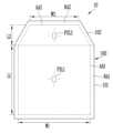
도 1a를 참조하면, 본 발명의 실시예에 의한 표시 장치(10)는 화소 영역(AA1, AA2)과 주변 영역(NA1, NA2)을 포함할 수 있다.Referring to FIG. 1A , a
화소 영역(AA1, AA2)에는 다수의 화소들(PXL1, PXL2)이 위치하며, 이에 따라 화소 영역(AA1, AA2)에서는 소정의 영상이 표시될 수 있다. 따라서, 화소 영역(AA1, AA2)은 표시 영역으로 지칭될 수 있다.A plurality of pixels PXL1 and PXL2 are positioned in the pixel areas AA1 and AA2, and accordingly, a predetermined image may be displayed in the pixel areas AA1 and AA2. Accordingly, the pixel areas AA1 and AA2 may be referred to as display areas.
주변 영역(NA1, NA2)에는 화소들(PXL1, PXL2)을 구동하기 위한 구성 요소들(예를 들어, 구동부 및 배선 등)이 위치할 수 있다. 주변 영역(NA1, NA2)에는 화소들(PXL1, PXL2)이 존재하지 않으므로, 상기 주변 영역(NA1, NA2)은 비표시 영역으로 지칭될 수 있다.Components for driving the pixels PXL1 and PXL2 (eg, a driving unit and wires) may be located in the peripheral areas NA1 and NA2 . Since the pixels PXL1 and PXL2 do not exist in the peripheral areas NA1 and NA2 , the peripheral areas NA1 and NA2 may be referred to as non-display areas.
예를 들어, 주변 영역(NA1, NA2)은 화소 영역(AA1, AA2)의 외측에 존재할 수 있으며, 화소 영역(AA1, AA2)의 적어도 일부를 둘러싸는 형태를 가질 수 있다.For example, the peripheral areas NA1 and NA2 may exist outside the pixel areas AA1 and AA2 and may have a shape surrounding at least a portion of the pixel areas AA1 and AA2 .
화소 영역(AA1, AA2)은 제1 화소 영역(AA1)과 제2 화소 영역(AA2)을 포함할 수 있다.The pixel areas AA1 and AA2 may include a first pixel area AA1 and a second pixel area AA2.
제2 화소 영역(AA2)은 제1 화소 영역(AA1)의 일측에 위치할 수 있으며, 제1 화소 영역(AA1)에 비해 작은 면적을 가질 수 있다.The second pixel area AA2 may be located on one side of the first pixel area AA1 and may have a smaller area than the first pixel area AA1.
예를 들어, 제2 화소 영역(AA2)의 폭(W2)은 제1 화소 영역(AA1)의 폭(W1)보다 작게 설정되고, 제2 화소 영역(AA2)의 길이(L2)는 제1 화소 영역(AA1)의 길이(L1)보다 작게 설정될 수 있다.For example, the width W2 of the second pixel area AA2 is smaller than the width W1 of the first pixel area AA1, and the length L2 of the second pixel area AA2 is the first pixel area AA2. It may be set smaller than the length L1 of the area AA1.
주변 영역(NA1, NA2)은 제1 주변 영역(NA1)과 제2 주변 영역(NA2)을 포함할 수 있다.The peripheral areas NA1 and NA2 may include a first peripheral area NA1 and a second peripheral area NA2 .
제1 주변 영역(NA1)은 제1 화소 영역(AA1)의 주변에 존재하며, 제1 화소 영역(AA1)의 적어도 일부를 둘러싸는 형태를 가질 수 있다.The first peripheral area NA1 is present around the first pixel area AA1 and may have a shape surrounding at least a portion of the first pixel area AA1.
제1 주변 영역(NA1)의 폭은 전체적으로 동일하게 설정될 수 있다. 다만, 이에 한정되는 것은 아니며, 제1 주변 영역(NA1)의 폭은 위치에 따라 상이하게 설정될 수 있다.The width of the first peripheral area NA1 may be set to be the same overall. However, it is not limited thereto, and the width of the first peripheral area NA1 may be differently set according to the position.
제2 주변 영역(NA2)은 제2 화소 영역(AA2)의 주변에 존재하며, 제2 화소 영역(AA2)의 적어도 일부를 둘러싸는 형태를 가질 수 있다.The second peripheral area NA2 is present around the second pixel area AA2 and may have a shape surrounding at least a portion of the second pixel area AA2.
제2 주변 영역(NA2)의 폭은 전체적으로 동일하게 설정될 수 있다. 다만, 이에 한정되는 것은 아니며, 제2 주변 영역(NA2)의 폭은 위치에 따라 상이하게 설정될 수 있다.The width of the second peripheral area NA2 may be set to be the same overall. However, it is not limited thereto, and the width of the second peripheral area NA2 may be set differently depending on the location.
화소들(PXL1, PXL2)은 제1 화소들(PXL1)과 제2 화소들(PXL2)을 포함할 수 있다.The pixels PXL1 and PXL2 may include first pixels PXL1 and second pixels PXL2 .
예를 들어, 제1 화소들(PXL1)은 제1 화소 영역(AA1)에 위치하고, 제2 화소들(PXL2)은 제2 화소 영역(AA2)에 위치할 수 있다.For example, the first pixels PXL1 may be positioned in the first pixel area AA1 and the second pixels PXL2 may be positioned in the second pixel area AA2 .
화소들(PXL1, PXL2)은 구동부의 제어에 따라 소정의 휘도로 발광할 수 있으며, 이를 위해 발광 소자(예를 들어, 유기 발광 다이오드)를 포함할 수 있다.The pixels PXL1 and PXL2 may emit light with a predetermined luminance according to the control of the driving unit, and may include a light emitting device (eg, an organic light emitting diode) for this purpose.
화소 영역(AA1, AA2)과 주변 영역(NA1, NA2)은 표시 장치(10)의 기판(100) 상에 정의될 수 있다.The pixel areas AA1 and AA2 and the peripheral areas NA1 and NA2 may be defined on the
기판(100)은 화소 영역(AA1, AA2)과 주변 영역(NA1, NA2)이 설정될 수 있는 다양한 형태로 형성될 수 있다.The
예를 들어, 기판(100)은 판형의 베이스 기판(101), 상기 베이스 기판(101)의 일단부로부터 일측으로 돌출 연장되는 보조판(102)을 포함할 수 있다.For example, the
이때, 보조판(102)은 베이스 기판(101) 보다 작은 면적을 가질 수 있다. 예를 들어 보조판(102)의 폭은 베이스 기판(101)의 폭보다 작게 설정되고, 보조판(102)의 길이는 베이스 기판(101)의 길이보다 작게 설정될 수 있다.In this case, the
보조판(102)은 제2 화소 영역(AA2)과 동일 또는 유사한 형태를 가질 수 있으나, 그에 제한되지는 않으며, 제2 화소 영역(AA2)과 상이한 형태를 가질 수도 있다.The
기판(100)은 유리, 수지(resin) 등과 같은 절연성 재료로 이루어질 수 있다. 또한, 기판(100)은 휘거나 접힘이 가능하도록 가요성(flexibility)을 갖는 재료로 이루어질 수 있고, 단층 구조 또는 다층 구조를 가질 수 있다.The
예를 들어, 기판(100)은 폴리스티렌(polystyrene), 폴리비닐알코올(polyvinyl alcohol), 폴리메틸메타크릴레이트(Polymethyl methacrylate), 폴리에테르술폰(polyethersulfone), 폴리아크릴레이트(polyacrylate), 폴리에테르이미드(polyetherimide), 폴리에틸렌 나프탈레이트(polyethylene naphthalate), 폴리에틸렌 테레프탈레이트(polyethylene terephthalate), 폴리페닐렌 설파이드(polyphenylene sulfide), 폴리아릴레이트(polyarylate), 폴리이미드(polyimide), 폴리카보네이트(polycarbonate), 트리아세테이트 셀룰로오스(triacetate cellulose), 셀룰로오스아세테이트 프로피오네이트(cellulose acetate propionate) 중 적어도 어느 하나를 포함할 수 있다.For example, the
다만, 기판(100)을 구성하는 재료는 다양하게 변화될 수 있으며, 유리 섬유 강화플라스틱(FRP, Fiber glass reinforced plastic) 등으로도 이루어질 수 있다.However, the material constituting the
제2 화소 영역(AA2)은 다양한 형상을 가질 수 있다. 예를 들어, 제2 화소 영역(AA2)은 다각형, 원형 등의 형상을 가질 수 있다. 또한, 제2 화소 영역(AA2)의 적어도 일부분은 곡선 모양을 가질 수 있다.The second pixel area AA2 may have various shapes. For example, the second pixel area AA2 may have a polygonal or circular shape. Also, at least a portion of the second pixel area AA2 may have a curved shape.
예를 들어, 제2 화소 영역(AA2)은 도 1a에 도시된 바와 같이 사각 형상을 가질 수 있다.For example, the second pixel area AA2 may have a quadrangular shape as shown in FIG. 1A .
또한, 도 1b를 참조하면, 제2 화소 영역(AA2)은 일측으로 갈수록 그 폭(W2)이 점차적으로 좁아지는 형태를 가질 수 있다.Also, referring to FIG. 1B , the second pixel area AA2 may have a shape in which the width W2 gradually decreases toward one side.
제2 화소 영역(AA2)의 형태 변화에 대응하여, 한 라인(행 또는 열)에 위치하는 제2 화소들(PXL2)의 개수는 그 위치에 따라 변화될 수 있다.Corresponding to the shape change of the second pixel area AA2 , the number of second pixels PXL2 positioned in one line (row or column) may change according to the position.
도 1b에 도시된 제2 화소 영역(AA2)의 경우, 제2 화소들(PXL2)의 개수가 수평라인 단위로 상이하게 설정될 수 있다. 예를 들어, 제1 화소 영역(AA1)에 인접한 수평라인일수록 더 많은 수의 제2 화소들(PXL2)이 배치될 수 있다.In the case of the second pixel area AA2 shown in FIG. 1B , the number of second pixels PXL2 may be differently set in units of horizontal lines. For example, a larger number of second pixels PXL2 may be disposed in a horizontal line adjacent to the first pixel area AA1 .
도 2는 본 발명의 일 실시예에 의한 표시 장치를 나타낸 도면이다. 도 2에 도시된 표시 장치(10)는 도 1a과 관련한 화소 영역(AA1, AA2)을 기반으로 하고 있으나, 도 1b와 같은 다른 형태의 화소 영역(AA1, AA2)에도 적용될 수 있다.2 is a diagram illustrating a display device according to an exemplary embodiment of the present invention. The
도 2를 참조하면, 본 발명의 일 실시예에 의한 표시 장치(10)는 제1 화소들(PXL1), 제2 화소들(PXL2), 및 표시 구동부(200)를 포함할 수 있다.Referring to FIG. 2 , the
제1 화소들(PXL1)은 제1 화소 영역(AA1)에 위치하며, 각각 제1 주사선(S1), 제1 발광 제어선(E1), 및 제1 데이터선(D1)과 연결될 수 있다.The first pixels PXL1 are positioned in the first pixel area AA1 and may be connected to the first scan line S1 , the first emission control line E1 , and the first data line D1 , respectively.
제2 화소들(PXL2)은 제2 화소 영역(AA2)에 위치하며, 각각 제2 주사선(S2), 제2 발광 제어선(E2), 및 제2 데이터선(D2)과 연결될 수 있다.The second pixels PXL2 are positioned in the second pixel area AA2 and may be connected to the second scan line S2 , the second emission control line E2 , and the second data line D2 , respectively.
필요에 따라, 화소들(PXL1, PXL2)은 복수개의 주사선들과 연결될 수 있다.If necessary, the pixels PXL1 and PXL2 may be connected to a plurality of scan lines.
표시 구동부(200)는 구동 신호들을 화소들(PXL1, PXL2)로 공급함으로써, 화소들(PXL1, PXL2)의 발광을 제어할 수 있다.The
예를 들어, 표시 구동부(200)는 주사 신호를 주사선들(S1, S2)을 통해 화소들(PXL1, PXL2)로 공급하고, 발광 제어 신호를 발광 제어선들(E1, E2)을 통해 화소들(PXL1, PXL2)로 공급하며, 데이터 신호를 데이터선들(D1, D2)을 통해 화소들(PXL1, PXL2)로 공급할 수 있다.For example, the
표시 구동부(200)는 그 전체 또는 일부가 기판(100) 상에 직접 실장되거나, 연성 회로 기판(Flexible Printed Circuit Board) 등과 같은 별도의 구성 요소(110)를 통해 기판(100)과 연결될 수 있다.The
예를 들어, 표시 구동부(200)의 설치는 칩 온 글래스(Chip On Glass), 칩 온 플라스틱(Chip On Plastic), 테이프 캐리어 패키지(Tape Carrier Package), 칩 온 필름(Chip On Film) 등 다양한 방식에 의하여 이루어질 수 있다.For example, the
한편, 도 2에서는 기판(100)과 별개로 형성된 표시 구동부(200)가 기판(100)에 연결되는 것으로 도시하였으나, 본 발명이 이에 제한되는 것은 아니다.Meanwhile, in FIG. 2 , the
예를 들어, 표시 구동부(200) 전체 또는 표시 구동부(200)의 구성 중 일부는 기판(100) 상에 직접 실장될 수도 있으며, 이 경우 기판(100)의 제1 주변 영역(NA1) 및 제2 주변 영역(NA2)에 위치될 수 있다.For example, the entire
도 3은 도 2에 도시된 표시 구동부를 보다 자세히 나타낸 도면이다.FIG. 3 is a view showing the display driving unit shown in FIG. 2 in more detail.
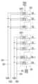
도 3을 참조하면, 본 발명의 실시예에 의한 표시 구동부(200)는 제1 주사 구동부(210), 제2 주사 구동부(220), 데이터 구동부(260), 타이밍 제어부(270), 제1 발광 구동부(310), 및 제2 발광 구동부(320)를 포함할 수 있다.Referring to FIG. 3 , the
제1 주사 구동부(210)는 제1 주사선들(S11~S1k)을 통하여 제1 화소들(PXL1)로 제1 주사 신호를 공급할 수 있다.The
예를 들어, 제1 주사 구동부(210)는 제1 주사 신호를 순차적으로 제1 주사선들(S11~S1k)에 공급할 수 있다.For example, the
제1 주사 구동부(210)가 기판(100) 상에 직접 실장되는 경우, 제1 주사 구동부(210)는 제1 주변 영역(NA1)에 위치할 수 있다.When the
제2 주사 구동부(220)는 제2 주사선들(S21~S2j)을 통하여 제2 화소들(PXL2)로 제2 주사 신호를 공급할 수 있다.The
예를 들어, 제2 주사 구동부(220)는 제2 주사 신호를 순차적으로 제2 주사선들(S21~S2j)에 공급할 수 있다.For example, the
제2 주사 구동부(220)가 기판(100) 상에 직접 실장되는 경우, 제2 주사 구동부(220)는 제2 주변 영역(NA2)에 위치할 수 있다.When the
주사 신호는 화소들(PXL1, PXL2)에 포함되는 트랜지스터가 턴-온될 수 있도록 게이트 온 전압(예를 들면, 로우 전압)으로 설정될 수 있다.The scan signal may be set to a gate-on voltage (eg, a low voltage) so that transistors included in the pixels PXL1 and PXL2 may be turned on.
제1 주사 구동부(210)와 제2 주사 구동부(220)는 각각 제1 주사 제어 신호(SCS1) 및 제2 주사 제어 신호(SCS2)에 대응하여 동작할 수 있다.The
데이터 구동부(260)는 제1 데이터선들(D11~D1o)을 통하여 제1 화소들(PXL1)로 데이터 신호를 공급할 수 있다.The
제1 화소들(PXL1)은 제1 화소 전원(ELVDD) 및 제2 화소 전원(ELVSS)에 접속될 수 있다. 필요에 따라, 제1 화소들(PXL1)은 초기화 전원(Vint)과 추가적으로 접속될 수 있다.The first pixels PXL1 may be connected to the first pixel power source ELVDD and the second pixel power source ELVSS. If necessary, the first pixels PXL1 may be additionally connected to the initialization power source Vint.
이와 같은 제1 화소들(PXL1)은 제1 주사선들(S11~S1k)로 제1 주사 신호가 공급될 때 제1 데이터선들(D11~D1o)로부터 데이터 신호를 공급받을 수 있으며, 데이터 신호를 공급받은 제1 화소들(PXL1)은 제1 화소 전원(ELVDD)으로부터 유기 발광 다이오드(미도시)를 경유하여 제2 화소 전원(ELVSS)으로 흐르는 전류량을 제어할 수 있다.When the first scan signal is supplied to the first scan lines S11 to S1k, the first pixels PXL1 may receive data signals from the first data lines D11 to D1o and supply the data signals. The received first pixels PXL1 may control the amount of current flowing from the first pixel power source ELVDD to the second pixel power source ELVSS via an organic light emitting diode (not shown).
또한, 한 라인(행 또는 열)에 위치하는 제1 화소들(PXL1)의 개수는 그 위치에 따라 변화할 수 있다.Also, the number of first pixels PXL1 positioned in one line (row or column) may change according to the position.
데이터 구동부(260)는 제2 데이터선들(D21~D2p)을 통하여 제2 화소들(PXL2)로 데이터 신호를 공급할 수 있다.The
예를 들어, 제2 데이터선들(D21~D2p)은 일부의 제1 데이터선들(D11~D1m-1)과 연결될 수 있다.For example, the second data lines D21 to D2p may be connected to some of the first data lines D11 to D1m-1.
또한, 제2 화소들(PXL2)은 제1 화소 전원(ELVDD) 및 제2 화소 전원(ELVSS)에 접속될 수 있다. 필요에 따라, 제2 화소들(PXL1)은 초기화 전원(Vint)과 추가적으로 접속될 수 있다.Also, the second pixels PXL2 may be connected to the first pixel power source ELVDD and the second pixel power source ELVSS. If necessary, the second pixels PXL1 may be additionally connected to the initialization power source Vint.
이와 같은 제2 화소들(PXL2)은 제2 주사선들(S21~S2j)로 제2 주사 신호가 공급될 때 제2 데이터선들(D21~D2p)로부터 데이터 신호를 공급받을 수 있으며, 데이터 신호를 공급받은 제2 화소들(PXL2)은 제1 화소 전원(ELVDD)으로부터 유기 발광 다이오드(미도시)를 경유하여 제2 화소 전원(ELVSS)으로 흐르는 전류량을 제어할 수 있다.When the second scan signal is supplied to the second scan lines S21 to S2j, the second pixels PXL2 may receive data signals from the second data lines D21 to D2p and supply the data signals. The received second pixels PXL2 may control the amount of current flowing from the first pixel power source ELVDD to the second pixel power source ELVSS via an organic light emitting diode (not shown).
또한, 한 라인(행 또는 열)에 위치하는 제2 화소들(PXL2)의 개수는 그 위치에 따라 변화할 수 있다.Also, the number of second pixels PXL2 positioned in one line (row or column) may change according to the position.
이때, 데이터 구동부(260)는 데이터 제어 신호(DCS)에 대응하여 동작할 수 있다.At this time, the
제1 발광 구동부(310)는 제1 발광 제어선들(E11~E1k)을 통하여 제1 화소들(PXL1)로 제1 발광 제어 신호를 공급할 수 있다.The first
예를 들어, 제1 발광 구동부(310)는 제1 발광 제어 신호를 순차적으로 제1 발광 제어선들(E11~E1k)에 공급할 수 있다.For example, the first
제1 발광 구동부(310)가 기판(100) 상에 직접 실장되는 경우, 제1 발광 구동부(310)는 제1 주변 영역(NA1)에 위치할 수 있다.When the first
제1 화소들(PXL1)이 제1 발광 제어 신호를 이용할 필요가 없는 구조인 경우, 제1 발광 구동부(310)와 제1 발광 제어선들(E11~E1k)은 생략될 수 있다.When the first pixels PXL1 do not need to use the first emission control signal, the
제2 발광 구동부(320)는 제2 발광 제어선들(E21~E2j)을 통하여 제2 화소들(PXL2)로 제2 발광 제어 신호를 공급할 수 있다.The second
예를 들어, 제2 발광 구동부(320)는 제2 발광 제어 신호를 순차적으로 제2 발광 제어선들(E21~E2j)에 공급할 수 있다.For example, the second
제2 발광 구동부(320)가 기판(100) 상에 직접 실장되는 경우, 제2 발광 구동부(320)는 제2 주변 영역(NA2)에 위치할 수 있다.When the second
제2 화소들(PXL2)이 제2 발광 제어 신호를 이용할 필요가 없는 구조인 경우, 제2 발광 구동부(320)와 제2 발광 제어선들(E21~E2j)은 생략될 수 있다.When the second pixels PXL2 do not need to use the second emission control signal, the
발광 제어 신호는 화소들(PXL1, PXL2)의 발광 시간을 제어하기 위하여 사용된다. 이를 위하여, 발광 제어신호는 주사신호보다 넓은 폭으로 설정될 수 있다.The emission control signal is used to control the emission time of the pixels PXL1 and PXL2. To this end, the emission control signal may be set to have a wider width than the scan signal.
예를 들어, 발광 제어 신호는 화소들(PXL1, PXL2)에 포함되는 트랜지스터가 턴-오프될 수 있도록 게이트 오프 전압(예를 들면, 하이 전압)으로 설정될 수 있다.For example, the emission control signal may be set to a gate-off voltage (eg, a high voltage) to turn off transistors included in the pixels PXL1 and PXL2 .
제1 발광 구동부(310)와 제2 발광 구동부(320)는 각각 제1 발광 제어 신호(ECS1) 및 제2 발광 제어 신호(ECS2)에 대응하여 동작할 수 있다.The first
제2 화소 영역(AA2)은 제1 화소 영역(AA1) 보다 작은 면적을 가지므로, 제2 화소들(PXL2)의 개수는 제1 화소들(PXL1)의 개수보다 적을 수 있으며, 제2 주사선들(S21~S2j)과 제2 발광 제어선들(E21~E2j)의 길이는 제1 주사선들(S11~S1k)과 제1 발광 제어선들(E11~E1k)에 비해 짧을 수 있다.Since the second pixel area AA2 has a smaller area than the first pixel area AA1, the number of second pixels PXL2 may be less than the number of first pixels PXL1, and the second scan lines The lengths of (S21 to S2j) and the second emission control lines (E21 to E2j) may be shorter than those of the first scan lines (S11 to S1k) and the first emission control lines (E11 to E1k).
제2 주사선들(S21~S2j) 중 어느 하나에 연결된 제2 화소들(PXL2)의 개수는 제1 주사선들(S11~S1k) 중 어느 하나에 연결된 제1 화소들(PXL1)의 개수보다 적을 수 있다.The number of second pixels PXL2 connected to any one of the second scan lines S21 to S2j may be less than the number of first pixels PXL1 connected to any one of the first scan lines S11 to S1k. there is.
또한, 제2 발광 제어선들(E21~E2j) 중 어느 하나에 연결된 제2 화소들(PXL2)의 개수는 제1 발광 제어선들(E11~E1k) 중 어느 하나에 연결된 제1 화소들(PXL1)의 개수보다 적을 수 있다.Also, the number of second pixels PXL2 connected to any one of the second emission control lines E21 to E2j is the number of first pixels PXL1 connected to any one of the first emission control lines E11 to E1k. may be less than the number of
타이밍 제어부(270)는 제1 주사 구동부(210), 제2 주사 구동부(220), 데이터 구동부(260), 제1 발광 구동부(310), 및 제2 발광 구동부(320)를 제어할 수 있다.The
이를 위하여, 타이밍 제어부(270)는 제1 주사 제어 신호(SCS1) 및 제2 주사 제어 신호(SCS2)를 각각 제1 주사 구동부(210)와 제2 주사 구동부(220)로 공급하고, 제1 발광 제어 신호(ECS1) 및 제2 발광 제어 신호(ECS2)를 각각 제1 발광 구동부(310)와 제2 발광 구동부(320)로 공급할 수 있다.To this end, the
이때, 주사 제어 신호들(SCS1, SCS2)와 발광 제어 신호들(ECS1, ECS2)은 각각 적어도 하나의 클럭 신호와 스타트 펄스를 포함할 수 있다.In this case, each of the scan control signals SCS1 and SCS2 and the emission control signals ECS1 and ECS2 may include at least one clock signal and a start pulse.
스타트 펄스는 첫번째 주사 신호 또는 첫번째 발광 제어 신호의 타이밍을 제어할 수 있다. 클럭 신호는 스타트 펄스를 쉬프트시키기 위하여 사용될 수 있다. The start pulse may control the timing of the first scan signal or the first emission control signal. A clock signal can be used to shift the start pulse.
또한, 타이밍 제어부(270)는 데이터 제어 신호(DCS)를 데이터 구동부(260)에 공급할 수 있다.Also, the
데이터 제어 신호(DCS)에는 소스 스타트 펄스 및 적어도 하나의 클럭 신호가 포함될 수 있다. 소스 스타트 펄스는 데이터의 샘플링 시작 시점을 제어하며, 클럭 신호는 샘플링 동작을 제어하기 위하여 사용될 수 있다.The data control signal DCS may include a source start pulse and at least one clock signal. The source start pulse controls data sampling start time, and the clock signal can be used to control the sampling operation.
한편, 제1 주사선들(S11~S1k)의 로드와 제2 주사선들(S21~S2j)의 로드는 상이할 수 있다.Meanwhile, the loads of the first scan lines S11 to S1k and the loads of the second scan lines S21 to S2j may be different.
즉, 제1 주사선들(S11~S1k)의 길이가 제2 주사선들(S21~S2j) 보다 길고, 제1 화소들(PXL1)의 개수가 제2 화소들(PXL2) 보다 많으므로, 제1 주사선들(S11~S1k)의 로드는 제2 주사선들(S21~S2j) 보다 크게 설정될 수 있다.That is, since the length of the first scan lines S11 to S1k is longer than the second scan lines S21 to S2j and the number of first pixels PXL1 is greater than that of the second pixels PXL2 , the first scan line The rods of the lines S11 to S1k may be set larger than those of the second scan lines S21 to S2j.
이는 제1 주사 신호 및 제2 주사 신호의 시정수(time constant) 차이를 야기하고, 결국 제1 주사 신호에는 제2 주사 신호에 비해 RC 딜레이(RC delay)가 크게 발생된다.This causes a time constant difference between the first scan signal and the second scan signal, and as a result, a larger RC delay is generated in the first scan signal than in the second scan signal.
이에 따라, 제1 화소들(PXL1)에 대한 데이터 기입 시간이 제2 화소들(PXL2)에 비해 짧아지게 되고, 이는 결국 제1 화소들(PXL1)과 제2 화소들(PXL2)의 휘도 차이를 발생시키게 된다.Accordingly, the data write time for the first pixels PXL1 becomes shorter than that for the second pixels PXL2 , which eventually reduces the luminance difference between the first pixels PXL1 and the second pixels PXL2 . will cause
그러므로, 본 발명의 실시예에서는 제1 주사 구동부(210)와 제2 주사 구동부(220)에 대하여 클럭선을 각각 분리 설치하고, 각 클럭선에 공급되는 클럭 신호의 특성을 상이하게 조절함으로써, 제1 화소들(PXL1)의 데이터 기입 시간과 제2 화소들(PXL2)의 데이터 기입 시간을 유사하게 설정할 수 있다.Therefore, in the embodiment of the present invention, clock lines are separately installed for the
이에 따라, 제1 화소 영역(AA1)과 제2 화소 영역(AA2)의 휘도 차는 개선될 수 있다.Accordingly, a luminance difference between the first pixel area AA1 and the second pixel area AA2 may be improved.
이하에서는 이와 관련된 본 발명의 구성을 보다 자세히 설명하도록 한다.Hereinafter, the configuration of the present invention related to this will be described in more detail.
도 4는 도 3에 도시된 제1 주사 구동부와 제2 주사 구동부를 보다 자세히 나타낸 도면이다.FIG. 4 is a view showing the first scan driver and the second scan driver shown in FIG. 3 in more detail.
도 4를 참조하면, 제1 클럭선(241)과 제2 클럭선(242)은 타이밍 제어부(270)와 제1 주사 구동부(210) 사이에 연결되고, 제3 클럭선(243)과 제4 클럭선(244)은 타이밍 제어부(270)와 제2 주사 구동부(220) 사이에 연결될 수 있다.Referring to FIG. 4 , the
제1 주사 구동부(210)와 관련된 제1, 2 클럭선들(241, 242)과, 제2 주사 구동부(220)와 관련된 제3, 4 클럭선들(243, 244)은 전기적으로 분리되어 위치할 수 있다.The first and
제1 클럭선(241)과 제2 클럭선(242)은 타이밍 제어부(270)로부터 공급되는 제1 클럭 신호(CLK1)와 제2 클럭 신호(CLK2)를 각각 제1 주사 구동부(210)로 전달하고, 제3 클럭선(243)과 제4 클럭선(244)은 타이밍 제어부(270)로부터 공급되는 제3 클럭 신호(CLK3)와 제4 클럭 신호(CLK4)를 각각 제2 주사 구동부(220)로 공급할 수 있다.The
이와 같이 클럭선을 분리 구성하는 경우, 제1 주사 구동부(210)와 제2 주사 구동부(220)가 동일한 클럭선을 공유하는 경우에 비하여 제1 주사선들(S11~S1k)의 로드가 일부 작아지므로, 제1 주사 신호의 RC 딜레이를 일부 줄일 수 있다.When the clock lines are separated in this way, the load of the first scan lines S11 to S1k is partially reduced compared to the case where the
제1 클럭 신호(CLK1)와 제2 클럭 신호(CLK2)는 서로 다른 위상(phase)을 가질 수 있다. 예를 들어, 제2 클럭 신호(CLK2)는 제1 클럭 신호(CLK1)와 180도의 위상차를 가질 수 있다.The first clock signal CLK1 and the second clock signal CLK2 may have different phases. For example, the second clock signal CLK2 may have a phase difference of 180 degrees from the first clock signal CLK1.
제3 클럭 신호(CLK3)와 제4 클럭 신호(CLK4)는 서로 다른 위상을 가질 수 있다. 예를 들어, 제3 클럭 신호(CLK3)는 제4 클럭 신호(CLK4)와 180도의 위상차를 가질 수 있다.The third clock signal CLK3 and the fourth clock signal CLK4 may have different phases. For example, the third clock signal CLK3 may have a phase difference of 180 degrees from the fourth clock signal CLK4.
제1 주사 구동부(210)는 다수의 주사 스테이지 회로들(SST11~SST1k)을 포함할 수 있다.The
제1 주사 구동부(210)의 주사 스테이지 회로들(SST11~SST1k)은 각각 제1 주사선들(S11~S1k)의 일단에 연결되고, 각각 제1 주사선들(S11~S1k)로 제1 주사 신호를 공급할 수 있다.The scan stage circuits SST11 to SST1k of the
이때, 주사 스테이지 회로들(SST11~SST1k)은 타이밍 제어부(270)로부터 공급되는 클럭 신호들(CLK1, CLK2)에 대응하여 동작될 수 있다. 또한, 주사 스테이지 회로들(SST11~SST1k)은 동일한 회로로 구현될 수 있다.At this time, the scan stage circuits SST11 to SST1k may operate in response to the clock signals CLK1 and CLK2 supplied from the
주사 스테이지 회로들(SST11~SST1k)은 이전 주사 스테이지 회로의 출력 신호(즉, 주사 신호) 또는 스타트 펄스(SSP1)를 공급받을 수 있다.The scan stage circuits SST11 to SST1k may receive an output signal (ie, a scan signal) or a start pulse SSP1 of a previous scan stage circuit.
예를 들어, 첫번째 주사 스테이지 회로(SST11)는 스타트 펄스(SSP1)를 공급받고, 나머지 주사 스테이지 회로들(SST12~SST1k)은 이전 스테이지 회로의 출력 신호를 공급받을 수 있다.For example, the first scan stage circuit SST11 may receive the start pulse SSP1, and the remaining scan stage circuits SST12 to SST1k may receive the output signal of the previous stage circuit.
다른 실시예에서, 제1 주사 구동부(210)의 첫번째 주사 스테이지 회로(SST11)는 제2 주사 구동부(220)의 마지막 주사 스테이지 회로(SST2j)로부터 출력되는 신호를 스타트 펄스로 사용할 수 있다.In another embodiment, the first scan stage circuit SST11 of the
주사 스테이지 회로들(SST11~SST1k)은 각각 제1 구동 전원(VDD1)과 제2 구동 전원(VSS1)을 공급받을 수 있다.The scan stage circuits SST11 to SST1k may receive the first driving power supply VDD1 and the second driving power supply VSS1, respectively.
여기서, 제1 구동 전원(VDD1)은 게이트 오프 전압, 예를 들면 하이 레벨의 전압으로 설정될 수 있다. 그리고, 제2 구동 전원(VSS1)은 게이트 온 전압, 예를 들면 로우 레벨의 전압으로 설정될 수 있다.Here, the first driving power supply VDD1 may be set to a gate-off voltage, for example, a high level voltage. Also, the second driving power source VSS1 may be set to a gate-on voltage, for example, a low-level voltage.
제2 주사 구동부(220)는 다수의 주사 스테이지 회로들(SST21~SST2j)을 포함할 수 있다.The
제2 주사 구동부(220)의 주사 스테이지 회로들(SST21~SST2j)은 각각 제2 주사선들(S21~S2j)의 일단에 연결되고, 각각 제2 주사선들(S21~S2j)로 제2 주사 신호를 공급할 수 있다.The scan stage circuits SST21 to SST2j of the
이때, 주사 스테이지 회로들(SST21~SST2j)은 타이밍 제어부(270)로부터 공급되는 클럭 신호들(CLK3, CLK4)에 대응하여 동작될 수 있다. 또한, 주사 스테이지 회로들(SST21~SST2j)은 동일한 회로로 구현될 수 있다.At this time, the scan stage circuits SST21 to SST2j may be operated in response to the clock signals CLK3 and CLK4 supplied from the
주사 스테이지 회로들(SST21~SST2j)은 이전 주사 스테이지 회로의 출력 신호(즉, 주사 신호) 또는 스타트 펄스(SSP2)를 공급받을 수 있다.The scan stage circuits SST21 to SST2j may receive an output signal (ie, a scan signal) or a start pulse SSP2 of a previous scan stage circuit.
예를 들어, 첫번째 주사 스테이지 회로(SST21)는 스타트 펄스(SSP2)를 공급받고, 나머지 주사 스테이지 회로들(SST22~SST2j)은 이전 스테이지 회로의 출력 신호를 공급받을 수 있다.For example, the first scan stage circuit SST21 may receive the start pulse SSP2, and the remaining scan stage circuits SST22 to SST2j may receive the output signal of the previous stage circuit.
또한, 제2 주사 구동부(220)의 마지막 주사 스테이지 회로(SST2j)는 제1 주사 구동부(210)의 첫번째 주사 스테이지 회로(SST11)로 출력 신호를 공급할 수 있다.Also, the last scan stage circuit SST2j of the
주사 스테이지 회로들(SST21~SST2j)은 각각 제1 구동 전원(VDD1)과 제2 구동 전원(VSS1)을 공급받을 수 있다.The scan stage circuits SST21 to SST2j may receive the first driving power supply VDD1 and the second driving power supply VSS1, respectively.
도 4에서는 주사 구동부들(210, 220)이 각각 2개의 클럭 신호들을 이용하는 것을 도시하였으나, 주사 스테이지 회로의 구조에 따라 상기 주사 구동부들(210, 220)이 이용하는 클럭 신호의 수는 변화될 수 있다.Although FIG. 4 shows that the
도 5는 본 발명의 일 실시예에 의한 제1 내지 제4 클럭 신호들 및 제1, 2 주사 신호들을 나타낸 파형도이다. 도 5에서는 설명의 편의를 위하여 첫번째 제1 주사선(S11) 및 두번째 제1 주사선(S12)에 공급되는 제1 주사 신호들과, 첫번째 제2 주사선(S21) 및 두번째 제2 주사선(S22)에 공급되는 제2 주사 신호들만을 도시하였다.5 is a waveform diagram illustrating first to fourth clock signals and first and second scan signals according to an embodiment of the present invention. In FIG. 5 , for convenience of description, the first scan signals supplied to the first first scan line S11 and the second first scan line S12 are supplied to the first second scan line S21 and the second second scan line S22. Only the second scan signals that are used are shown.
도 5를 참조하면, 본 발명의 실시예에 의한 타이밍 제어부(270)는 신호 특성이 동일한 클럭 신호들(CLK1, CLK2, CLK3, CLK4)을 공급할 수 있다.Referring to FIG. 5 , the
클럭 신호들(CLK1, CLK2, CLK3, CLK4)은 로우 전압인 제1 전압(V1)과 하이 전압인 제2 전압(V2) 사이를 스윙하는 클럭 신호일 수 있다.The clock signals CLK1 , CLK2 , CLK3 , and CLK4 may be clock signals that swing between a first voltage V1 , which is a low voltage, and a second voltage V2 , which is a high voltage.
예를 들어, 제1 클럭 신호(CLK1)는 제3 클럭 신호(CLK3)와 동일한 신호로 설정될 수 있고, 제2 클럭 신호(CLK2)는 제4 클럭 신호(CLK4)와 동일한 신호로 설정될 수 있다.For example, the first clock signal CLK1 may be set to the same signal as the third clock signal CLK3, and the second clock signal CLK2 may be set to the same signal as the fourth clock signal CLK4. there is.
제1 주사 구동부(210)와 제2 주사 구동부(220)에 동일한 신호 특성을 갖는 클럭 신호들(CLK1, CLK2, CLK3, CLK4)을 공급하는 경우, 제1 화소 영역(AA1)에 존재하는 높은 로드로 인하여, 제1 주사 신호의 지연 현상이 제2 주사 신호에 비해 크게 나타날 수 있다.When the clock signals CLK1 , CLK2 , CLK3 , and CLK4 having the same signal characteristics are supplied to the
즉, 클럭선을 분리 구성함으로써 제1 화소 영역(AA1)과 제2 화소 영역(AA2)의 휘도 차를 일부 개선할 수 있으나, 제1 화소 영역(AA1)과 제2 화소 영역(AA2)의 로드 차이가 큰 경우 휘도 차에 대한 추가적인 보상이 필요할 수 있다.That is, the luminance difference between the first pixel area AA1 and the second pixel area AA2 may be partially improved by separating the clock lines, but the load between the first and second pixel areas AA1 and AA2 may be reduced. If the difference is large, additional compensation for the luminance difference may be required.
이 경우, 본 발명의 실시예에 의한 타이밍 제어부(270)는 클럭 신호들(CLK1, CLK2, CLK3, CLK4)의 특성을 상이하게 설정함으로써, 휘도 차를 추가적으로 개선할 수 있다.In this case, the
이때, 타이밍 제어부(270)에 의해 제어될 수 있는 클럭 신호의 특성은 펄스폭, 상승 에지 기간의 길이 및 하강 에지 기간의 길이 중 적어도 하나를 포함할 수 있다.In this case, the characteristics of the clock signal controllable by the
도 6은 본 발명의 일 실시예에 의한 제3, 4 클럭 신호들 및 제2 주사 신호를 나타낸 파형도이다. 도 6에서는 설명의 편의를 위하여 첫번째 제2 주사선(S21) 및 두번째 제2 주사선(S22)에 공급되는 제2 주사 신호들만을 도시하였다.6 is a waveform diagram illustrating third and fourth clock signals and a second scan signal according to an embodiment of the present invention. In FIG. 6 , only the second scan signals supplied to the first second scan line S21 and the second second scan line S22 are illustrated for convenience of description.
도 5 및 도 6을 참조하면, 제3 클럭 신호(CLK3)의 펄스폭(Pw3)은 제1 클럭 신호(CLK1)의 펄스폭(Pw1)과 상이하게 설정될 수 있다.Referring to FIGS. 5 and 6 , the pulse width Pw3 of the third clock signal CLK3 may be set to be different from the pulse width Pw1 of the first clock signal CLK1.
예를 들어, 제3 클럭 신호(CLK3)의 펄스폭(Pw3)은 제1 클럭 신호(CLK1)의 펄스폭(Pw1)보다 작게 설정될 수 있다.For example, the pulse width Pw3 of the third clock signal CLK3 may be set smaller than the pulse width Pw1 of the first clock signal CLK1.
또한, 제4 클럭 신호(CLK4)의 펄스폭(Pw4)은 제2 클럭 신호(CLK2)의 펄스폭(Pw2)과 상이하게 설정될 수 있다.Also, the pulse width Pw4 of the fourth clock signal CLK4 may be set to be different from the pulse width Pw2 of the second clock signal CLK2.
예를 들어, 제4 클럭 신호(CLK4)의 펄스폭(Pw4)은 제2 클럭 신호(CLK2)의 펄스폭(Pw2)보다 작게 설정될 수 있다.For example, the pulse width Pw4 of the fourth clock signal CLK4 may be set smaller than the pulse width Pw2 of the second clock signal CLK2.
제1 클럭 신호(CLK1)의 펄스폭(Pw1)과 제2 클럭 신호(CLK2)의 펄스폭(Pw2)은 동일할 수 있고, 제3 클럭 신호(CLK3)의 펄스폭(Pw3)과 제4 클럭 신호(CLK4)의 펄스폭(Pw4)은 동일할 수 있다.The pulse width Pw1 of the first clock signal CLK1 and the pulse width Pw2 of the second clock signal CLK2 may be the same, and the pulse width Pw3 of the third clock signal CLK3 and the pulse width Pw2 of the fourth clock signal CLK3 may be the same. The pulse width Pw4 of the signal CLK4 may be the same.
제2 주사 구동부(220)에 공급되는 클럭 신호들(CLK3, CLK4)의 펄스폭(Pw3, Pw4)를 줄임으로써, 도 6에 도시된 바와 같이 제2 주사 신호의 공급 기간(또는 펄스폭)도 줄어들게 된다.By reducing the pulse widths Pw3 and Pw4 of the clock signals CLK3 and CLK4 supplied to the
그러므로, 제2 화소들(PXL2)의 데이터 기입 시간은 제1 화소들(PXL1)의 데이터 기입 시간과 유사하게 조절될 수 있으며, 이에 따라 제1 화소 영역(AA1)과 제2 화소 영역(AA2)의 휘도 차는 줄어들 수 있다.Therefore, the data writing time of the second pixels PXL2 may be adjusted similarly to that of the first pixels PXL1 , and accordingly, the first pixel area AA1 and the second pixel area AA2 may be adjusted. The luminance difference of can be reduced.
도 7은 본 발명의 다른 실시예에 의한 제3, 4 클럭 신호들 및 제2 주사 신호를 나타낸 파형도이다. 도 7에서는 설명의 편의를 위하여 첫번째 제2 주사선(S21) 및 두번째 제2 주사선(S22)에 공급되는 제2 주사 신호들만을 도시하였다.7 is a waveform diagram illustrating third and fourth clock signals and a second scan signal according to another embodiment of the present invention. In FIG. 7 , only the second scan signals supplied to the first second scan line S21 and the second second scan line S22 are illustrated for convenience of description.
도 5 및 도 7을 참조하면, 제3 클럭 신호(CLK3)의 하강 에지 기간(F3)은 제1 클럭 신호(CLK1)의 하강 에지 기간(F1)과 상이하게 설정될 수 있다.5 and 7 , the falling edge period F3 of the third clock signal CLK3 may be set differently from the falling edge period F1 of the first clock signal CLK1.
예를 들어, 제3 클럭 신호(CLK3)의 하강 에지 기간(F3)은 제1 클럭 신호(CLK1)의 하강 에지 기간(F1)보다 길게 설정될 수 있다.For example, the falling edge period F3 of the third clock signal CLK3 may be longer than the falling edge period F1 of the first clock signal CLK1.
또한, 제3 클럭 신호(CLK3)의 상승 에지 기간(R3)은 제1 클럭 신호(CLK1)의 상승 에지 기간(R1)과 상이하게 설정될 수 있다.Also, the rising edge period R3 of the third clock signal CLK3 may be set differently from the rising edge period R1 of the first clock signal CLK1.
예를 들어, 제3 클럭 신호(CLK3)의 상승 에지 기간(R3)은 제1 클럭 신호(CLK1)의 상승 에지 기간(R1)보다 길게 설정될 수 있다.For example, the rising edge period R3 of the third clock signal CLK3 may be longer than the rising edge period R1 of the first clock signal CLK1.
도 5에 도시된 제1 클럭 신호(CLK1)는 이상적인 클럭 신호로서, 하강 에지 기간(F1)과 상승 에지 기간(R1)의 길이는 "0"으로 설정될 수 있다. 그러나, 실제 제1 클럭 신호(CLK1)는 제1 클럭선(241)의 RC 성분에 의하여 소정의 길이를 갖는 하강 에지 기간(F1)과 상승 에지 기간(R1)을 가질 수 있다.The first clock signal CLK1 shown in FIG. 5 is an ideal clock signal, and the lengths of the falling edge period F1 and the rising edge period R1 may be set to “0”. However, the actual first clock signal CLK1 may have a falling edge period F1 and a rising edge period R1 having predetermined lengths according to the RC component of the
한편, 제4 클럭 신호(CLK4)의 하강 에지 기간(F4)은 제2 클럭 신호(CLK2)의 하강 에지 기간(F2)과 상이하게 설정될 수 있다.Meanwhile, the falling edge period F4 of the fourth clock signal CLK4 may be set differently from the falling edge period F2 of the second clock signal CLK2.
예를 들어, 제4 클럭 신호(CLK4)의 하강 에지 기간(F4)은 제2 클럭 신호(CLK2)의 하강 에지 기간(F2)보다 길게 설정될 수 있다.For example, the falling edge period F4 of the fourth clock signal CLK4 may be longer than the falling edge period F2 of the second clock signal CLK2.
또한, 제4 클럭 신호(CLK4)의 상승 에지 기간(R4)은 제2 클럭 신호(CLK2)의 상승 에지 기간(R2)과 상이하게 설정될 수 있다.Also, the rising edge period R4 of the fourth clock signal CLK4 may be set differently from the rising edge period R2 of the second clock signal CLK2.
예를 들어, 제4 클럭 신호(CLK4)의 상승 에지 기간(R4)은 제2 클럭 신호(CLK2)의 상승 에지 기간(R2)보다 길게 설정될 수 있다.For example, the rising edge period R4 of the fourth clock signal CLK4 may be longer than the rising edge period R2 of the second clock signal CLK2.
도 5에 도시된 제2 클럭 신호(CLK2)는 이상적인 클럭 신호로서, 하강 에지 기간(F2)과 상승 에지 기간(R2)의 길이는 "0"으로 설정될 수 있다. 그러나, 실제 제2 클럭 신호(CLK2)는 제2 클럭선(242)의 RC 성분에 의하여 소정의 길이를 갖는 하강 에지 기간(F2)과 상승 에지 기간(R2)을 가질 수 있다.The second clock signal CLK2 shown in FIG. 5 is an ideal clock signal, and the lengths of the falling edge period F2 and the rising edge period R2 may be set to “0”. However, the actual second clock signal CLK2 may have a falling edge period F2 and a rising edge period R2 having predetermined lengths according to the RC component of the
제1 클럭 신호(CLK1)의 하강 에지 기간(F1)과 상승 에지 기간(R1)은 각각 제2 클럭 신호(CLK2)의 하강 에지 기간(F2) 및 상승 에지 기간(R2)과 동일한 길이를 가질 수 있다.The falling edge period F1 and the rising edge period R1 of the first clock signal CLK1 may have the same length as the falling edge period F2 and the rising edge period R2 of the second clock signal CLK2, respectively. there is.
제3 클럭 신호(CLK3)의 하강 에지 기간(F3)과 상승 에지 기간(R3)은 각각 제4 클럭 신호(CLK4)의 하강 에지 기간(F4) 및 상승 에지 기간(R4)과 동일한 길이를 가질 수 있다.The falling edge period F3 and the rising edge period R3 of the third clock signal CLK3 may have the same length as the falling edge period F4 and the rising edge period R4 of the fourth clock signal CLK4, respectively. there is.
제3 클럭 신호(CLK3)와 제4 클럭 신호(CLK4)는 하강 에지 기간(F3, F4) 동안 각각 제2 전압(V2, 하이 전압)으로부터 제3 전압(V3, 중간 전압)을 거쳐 제1 전압(V1, 로우 전압)으로 변화될 수 있다.The third clock signal CLK3 and the fourth clock signal CLK4 generate the first voltage from the second voltage V2 (high voltage) through the third voltage V3 (mid voltage) during the falling edge periods F3 and F4, respectively. (V1, low voltage).
또한, 제3 클럭 신호(CLK3)와 제4 클럭 신호(CLK4)는 상승 에지 기간(R3, R4) 동안 각각 제1 전압(V1, 로우 전압)으로부터 제3 전압(V3, 중간 전압)을 거쳐 제2 전압(V2, 하이 전압)으로 변화될 수 있다.In addition, the third clock signal CLK3 and the fourth clock signal CLK4 are respectively divided from the first voltage V1 (low voltage) through the third voltage V3 (mid voltage) during the rising edge periods R3 and R4. 2 voltage (V2, high voltage).
이에 따라, 제3 클럭 신호(CLK3)와 제4 클럭 신호(CLK4)는 제1 전압(V1)과 제2 전압(V2) 사이를 스윙하며, 제3 전압(V3)을 경유하는 계단파 형태를 가질 수 있다.Accordingly, the third clock signal CLK3 and the fourth clock signal CLK4 swing between the first voltage V1 and the second voltage V2 and form a step wave passing through the third voltage V3. can have
예를 들어, 제1 전압(V1)은 음전압으로 설정되고, 제2 전압(V2)은 양전압으로 설정되며, 제3 전압(V3)은 그라운드 전압으로 설정될 수 있다.For example, the first voltage V1 may be set as a negative voltage, the second voltage V2 may be set as a positive voltage, and the third voltage V3 may be set as a ground voltage.
도 7에서는 제3, 4 클럭 신호들(CLK3, CLK4)의 하강 에지 기간(F3, F4)과 상승 에지 기간(R3, R4)을 모두 조절한 실시예를 도시하였으나, 하강 에지 기간(F3, F4)과 상승 에지 기간(R3, R4) 중 어느 하나만을 조절할 수도 있다.Although FIG. 7 shows an embodiment in which both the falling edge periods F3 and F4 and the rising edge periods R3 and R4 of the third and fourth clock signals CLK3 and CLK4 are adjusted, the falling edge periods F3 and F4 ) and one of the rising edge periods R3 and R4 may be adjusted.
제2 주사 구동부(220)에 공급되는 클럭 신호들(CLK3, CLK4)의 하강 에지 기간(F3, F4) 및/또는 상승 에지 기간(R3, R4)을 길게 연장시킴으로써, 도 7에 도시된 바와 같이 제2 주사 신호의 공급 기간(또는 펄스폭)도 줄어들게 되며, 제2 주사 신호는 도 5에 도시된 제1 주사 신호와 유사한 형태로 변화하게 된다.By lengthening the falling edge periods F3 and F4 and/or the rising edge periods R3 and R4 of the clock signals CLK3 and CLK4 supplied to the
그러므로, 제2 화소들(PXL2)의 데이터 기입 시간은 제1 화소들(PXL1)의 데이터 기입 시간과 유사하게 조절될 수 있으며, 이에 따라 제1 화소 영역(AA1)과 제2 화소 영역(AA2)의 휘도 차는 줄어들 수 있다.Therefore, the data writing time of the second pixels PXL2 may be adjusted similarly to that of the first pixels PXL1 , and accordingly, the first pixel area AA1 and the second pixel area AA2 may be adjusted. The luminance difference of can be reduced.
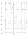
도 8은 도 4에 도시된 주사 스테이지 회로의 일 실시예를 나타낸 도면이다.FIG. 8 is a diagram illustrating one embodiment of the scan stage circuit shown in FIG. 4 .
도 8에서는 설명의 편의를 위하여, 제1 주사 구동부(210)의 주사 스테이지 회로들(SST11, SST12)을 도시하기로 한다.In FIG. 8 , scan stage circuits SST11 and SST12 of the
도 8을 참조하면, 첫번째 주사 스테이지 회로(SST11)는 제1 구동 회로(1210), 제2 구동 회로(1220), 및 출력부(1230)를 포함할 수 있다.Referring to FIG. 8 , the first scan stage circuit SST11 may include a
출력부(1230)는 제1 노드(N1) 및 제2 노드(N2)의 전압에 대응하여 출력 단자(1006)로 공급되는 전압을 제어할 수 있다. 이를 위하여, 출력부(1230)는 제5 트랜지스터(M5) 및 제6 트랜지스터(M6)를 포함할 수 있다.The
제5 트랜지스터(M5)는 제1 구동 전원(VDD1)이 입력되는 제4 입력 단자(1004)와 출력 단자(1006) 사이에 연결되며, 게이트 전극이 제1 노드(N1)에 연결될 수 있다. 이와 같은 제5 트랜지스터(M5)는 제1 노드(N1)에 인가되는 전압에 대응하여 제4 입력 단자(1004)와 출력 단자(1006)의 접속을 제어할 수 있다.The fifth transistor M5 is connected between the
제6 트랜지스터(M6)는 출력 단자(1006)와 제3 입력 단자(1003) 사이에 연결되며, 게이트 전극이 제2 노드(N2)에 연결될 수 있다. 이와 같은 제6 트랜지스터(M6)는 제2 노드(N2)에 인가되는 전압에 대응하여 출력 단자(1006)와 제3 입력 단자(1003)의 접속을 제어할 수 있다.The sixth transistor M6 is connected between the
이와 같은 출력부(1230)는 버퍼로 구동될 수 있다. 추가적으로, 제5 트랜지스터(M5) 및/또는 제6 트랜지스터(M6)는 상호 병렬 연결된 복수의 트랜지스터로 이루어질 수 있다.Such an
제1 구동 회로(1210)는 제1 입력 단자(1001) 내지 제3 입력 단자(1003)로 공급되는 신호들에 대응하여 제3 노드(N3)의 전압을 제어할 수 있다.The
이를 위하여, 제1 구동 회로(1210)는 제2 트랜지스터(M2) 내지 제4 트랜지스터(M4)를 포함할 수 있다. To this end, the
제2 트랜지스터(M2)는 제1 입력 단자(1001)와 제3 노드(N3) 사이에 연결되며, 게이트 전극이 제2 입력 단자(1002)에 연결될 수 있다. 이와 같은 제2 트랜지스터(M2)는 제2 입력 단자(1002)로 공급되는 신호에 대응하여 제1 입력 단자(1001)와 제3 노드(N3)의 접속을 제어할 수 있다.The second transistor M2 is connected between the
제3 트랜지스터(M3)와 제4 트랜지스터(M4)는 제3 노드(N3)와 제4 입력 단자(1004) 사이에 직렬로 연결될 수 있다. 실제로, 제3 트랜지스터(M3)는 제4 트랜지스터(M4)와 제3 노드(N3) 사이에 연결되며, 게이트 전극이 제3 입력 단자(1003)에 연결될 수 있다. 이와 같은 제3 트랜지스터(M3)는 제3 입력 단자(1003)로 공급되는 신호에 대응하여 제4 트랜지스터(M4)와 제3 노드(N3)의 접속을 제어할 수 있다.The third transistor M3 and the fourth transistor M4 may be connected in series between the third node N3 and the
제4 트랜지스터(M4)는 제3 트랜지스터(M3)와 제4 입력 단자(1004) 사이에 연결되며, 게이트 전극이 제1 노드(N1)에 연결될 수 있다. 이와 같은 제4 트랜지스터(M4)는 제1 노드(N1)의 전압에 대응하여 제3 트랜지스터(M3)와 제4 입력 단자(1004)의 접속을 제어할 수 있다.The fourth transistor M4 is connected between the third transistor M3 and the
제2 구동 회로(1220)는 제2 입력 단자(1002) 및 제3 노드(N3)의 전압에 대응하여 제1 노드(N1)의 전압을 제어할 수 있다. 이를 위하여, 제2 구동 회로(1220)는 제1 트랜지스터(M1), 제7 트랜지스터(M7), 제8 트랜지스터(M8), 제1 커패시터(C1) 및 제2 커패시터(C2)를 포함할 수 있다.The
제1 커패시터(C1)는 제2 노드(N2)와 출력 단자(1006) 사이에 연결될 수 있다. 이와 같은 제1 커패시터(C1)는 제6 트랜지스터(M6)의 턴-온 및 턴-오프에 대응하는 전압을 충전한다.A first capacitor C1 may be connected between the second node N2 and the
제2 커패시터(C2)는 제1 노드(N1)와 제4 입력 단자(1004) 사이에 연결될 수 있다. 이와 같은 제2 커패시터(C2)는 제1 노드(N1)에 인가되는 전압을 충전할 수 있다.The second capacitor C2 may be connected between the first node N1 and the
제7 트랜지스터(M7)는 제1 노드(N1)와 제2 입력 단자(1002) 사이에 연결되며, 게이트 전극이 제3 노드(N3)에 연결될 수 있다. 이와 같은 제7 트랜지스터(M7)는 제3 노드(N3)의 전압에 대응하여 제1 노드(N1)와 제2 입력 단자(1002)의 접속을 제어할 수 있다.The seventh transistor M7 is connected between the first node N1 and the
제8 트랜지스터(M8)는 제1 노드(N1)와 제2 구동 전원(VSS1)이 공급되는 제5 입력 단자(1005) 사이에 위치되며, 게이트 전극이 제2 입력 단자(1002)에 연결될 수 있다. 이와 같은 제8 트랜지스터(M8)는 제2 입력 단자(1002)의 신호에 대응하여 제1 노드(N1)와 제5 입력 단자(1005)의 접속을 제어할 수 있다.The eighth transistor M8 is positioned between the first node N1 and the
제1 트랜지스터(M1)는 제3 노드(N3)와 제2 노드(N2) 사이에 연결되며, 게이트 전극이 제5 입력 단자(1005)에 연결될 수 있다. 이와 같은 제1 트랜지스터(M1)는 턴-온 상태를 유지하면서 제3 노드(N3) 및 제2 노드(N2)의 전기적 접속을 유지할 수 있다. 추가적으로 제1 트랜지스터(M1)는 제2 노드(N2)의 전압에 대응하여 제3 노드(N3)의 전압 하강 폭을 제한할 수 있다. 다시 말하여, 제2 노드(N2)의 전압이 제2 구동 전원(VSS1)보다 낮은 전압으로 하강하더라도 제3 노드(N3)의 전압은 제2 구동 전원(VSS1)에서 제1 트랜지스터(M1)의 문턱전압을 감한 전압보다 낮아지지 않는다. 이와 관련한 자세한 설명은 후술하기로 한다.The first transistor M1 is connected between the third node N3 and the second node N2 and has a gate electrode connected to the
두번째 주사 스테이지 회로(SST12)와 나머지 주사 스테이지 회로들(SST13~SST1k)는 상기 첫번째 주사 스테이지 회로(SST11)과 동일한 구성을 가질 수 있다.The second scan stage circuit SST12 and the remaining scan stage circuits SST13 to SST1k may have the same configuration as the first scan stage circuit SST11.
또한, j(j는 홀수 또는 짝수)번째 주사 스테이지 회로(SST1j)의 제2 입력 단자(1002)는 제1 클럭 신호(CLK1), 제3 입력 단자(1003)는 제2 클럭 신호(CLK2)를 공급받을 수 있다. j+1번째 주사 스테이지 회로(SST1j+1)의 제2 입력 단자(1002)는 제2 클럭 신호(CLK2), 제3 입력 단자(1003)는 제1 클럭 신호(CLK1)를 공급받을 수 있다.In addition, the
도 7에서는 제1 주사 구동부(210)에 포함된 스테이지 회로를 대상으로 설명하였으나, 제2 주사 구동부(220)에 포함된 스테이지 회로들도 동일한 구성을 가질 수 있다.Although the stage circuit included in the
다만, 제2 주사 구동부(220)는 제1 클럭 신호(CLK1) 및 제2 클럭 신호(CLK2) 대신 제3 클럭 신호(CLK3)와 제4 클럭 신호(CLK4)를 이용할 수 있다.However, the
도 9는 도 2에 도시된 제1 화소의 일 실시예를 나타낸 도면이다.FIG. 9 is a diagram illustrating an example of a first pixel shown in FIG. 2 .
도 9에서는 설명의 편의를 위하여 m번째 제1 데이터선(D1m) 및 i번째 제1 주사선(S1i)에 접속된 제1 화소(PXL1)를 도시하기로 한다.9 illustrates the first pixel PXL1 connected to the m-th first data line D1m and the ith first scan line S1i for convenience of description.
도 9를 참조하면, 본 발명의 실시예에 의한 제1 화소(PXL1)는 유기 발광 다이오드(OLED), 제1 트랜지스터(T1) 내지 제7 트랜지스터(T7) 및 스토리지 커패시터(Cst)를 포함할 수 있다.Referring to FIG. 9 , the first pixel PXL1 according to an embodiment of the present invention may include an organic light emitting diode (OLED), first to seventh transistors T1 to T7, and a storage capacitor Cst. there is.
유기 발광 다이오드(OLED)의 애노드는 제6 트랜지스터(T6)를 경유하여 제1 트랜지스터(T1)에 접속되고, 캐소드는 제2 화소 전원(ELVSS)에 접속될 수 있다. 이와 같은 유기 발광 다이오드(OLED)는 제1 트랜지스터(T1)로부터 공급되는 전류량에 대응하여 소정 휘도의 빛을 생성할 수 있다.An anode of the organic light emitting diode OLED may be connected to the first transistor T1 via a sixth transistor T6 , and a cathode may be connected to the second pixel power source ELVSS. Such an organic light emitting diode (OLED) can generate light with a predetermined luminance in response to the amount of current supplied from the first transistor (T1).
유기 발광 다이오드(OLED)로 전류가 흐를 수 있도록 제1 화소 전원(ELVDD)은 제2 화소 전원(ELVSS)보다 높은 전압으로 설정될 수 있다.The first pixel power source ELVDD may be set to a higher voltage than the second pixel power source ELVSS so that current can flow through the organic light emitting diode OLED.
예를 들어, 제1 화소 전원(ELVDD)은 양전압으로 설정되고, 제2 화소 전원(ELVSS)은 음전압으로 설정될 수 있다.For example, the first pixel power source ELVDD may be set to a positive voltage, and the second pixel power source ELVSS may be set to a negative voltage.
제7 트랜지스터(T7)는 초기화 전원(Vint)과 유기 발광 다이오드(OLED)의 애노드 사이에 접속될 수 있다. 그리고, 제7 트랜지스터(T7)의 게이트 전극은 i번째 제1 주사선(S1i)에 접속될 수 있다. 이와 같은 제7 트랜지스터(T7)는 i번째 제1 주사선(S1i)으로 주사신호가 공급될 때 턴-온되어 초기화 전원(Vint)의 전압을 유기 발광 다이오드(OLED)의 애노드로 공급할 수 있다. 여기서, 초기화 전원(Vint)은 데이터 신호보다 낮은 전압으로 설정될 수 있다.The seventh transistor T7 may be connected between the initialization power source Vint and the anode of the organic light emitting diode OLED. Also, a gate electrode of the seventh transistor T7 may be connected to the i-th first scan line S1i. The seventh transistor T7 is turned on when a scan signal is supplied to the i-th first scan line S1i and supplies the voltage of the initialization power source Vint to the anode of the organic light emitting diode OLED. Here, the initialization power source Vint may be set to a voltage lower than that of the data signal.
제6 트랜지스터(T6)는 제1 트랜지스터(T1)와 유기 발광 다이오드(OLED) 사이에 접속될 수 있다. 그리고, 제6 트랜지스터(T6) 게이트 전극은 i번째 제1 발광 제어선(E1i)에 접속될 수 있다. 이와 같은 제6 트랜지스터(T6)는 i번째 제1 발광 제어선(E1i)으로 발광 제어신호가 공급될 때 턴-오프되고, 그 외의 경우에 턴-온될 수 있다.The sixth transistor T6 may be connected between the first transistor T1 and the organic light emitting diode OLED. Also, the gate electrode of the sixth transistor T6 may be connected to the i-th first emission control line E1i. The sixth transistor T6 is turned off when an emission control signal is supplied to the i-th first emission control line E1i, and may be turned on in other cases.
제5 트랜지스터(T5)는 제1 화소 전원(ELVDD)과 제1 트랜지스터(T1) 사이에 접속될 수 있다. 그리고, 제5 트랜지스터(T5)의 게이트 전극은 i번째 제1 발광 제어선(E1i)에 접속될 수 있다. 이와 같은 제5 트랜지스터(T5)는 i번째 제1 발광 제어선(E1i)으로 발광 제어신호가 공급될 때 턴-오프되고, 그 외의 경우에 턴-온될 수 있다.The fifth transistor T5 may be connected between the first pixel power source ELVDD and the first transistor T1. Also, a gate electrode of the fifth transistor T5 may be connected to the i-th first emission control line E1i. The fifth transistor T5 is turned off when an emission control signal is supplied to the i-th first emission control line E1i, and may be turned on in other cases.
제1 트랜지스터(T1; 구동 트랜지스터)의 제1 전극은 제5 트랜지스터(T5)를 경유하여 제1 화소 전원(ELVDD)에 접속되고, 제 2전극은 제6 트랜지스터(T6)를 경유하여 유기 발광 다이오드(OLED)의 애노드에 접속될 수 있다. 그리고, 제1 트랜지스터(T1)의 게이트 전극은 제10 노드(N10)에 접속될 수 있다. 이와 같은 제1 트랜지스터(T1)는 제10 노드(N10)의 전압에 대응하여, 제1 화소 전원(ELVDD)으로부터 유기 발광 다이오드(OLED)를 경유하여 제2 화소 전원(ELVSS)으로 흐르는 전류량을 제어할 수 있다.The first electrode of the first transistor T1 (driving transistor) is connected to the first pixel power source ELVDD via the fifth transistor T5, and the second electrode is connected to the organic light emitting diode via the sixth transistor T6. (OLED) can be connected to the anode. Also, the gate electrode of the first transistor T1 may be connected to the tenth node N10. The first transistor T1 controls the amount of current flowing from the first pixel power source ELVDD to the second pixel power source ELVSS via the organic light emitting diode OLED in response to the voltage of the tenth node N10. can do.
제3 트랜지스터(T3)는 제1 트랜지스터(T1)의 제2 전극과 제10 노드(N10) 사이에 접속될 수 있다. 그리고, 제3 트랜지스터(T3)의 게이트 전극은 i번째 제1 주사선(S1i)에 접속될 수 있다. 이와 같은 제3 트랜지스터(T3)는 i번째 제1 주사선(S1i)으로 주사신호가 공급될 때 턴-온되어 제1 트랜지스터(T1)의 제2 전극과 제10 노드(N10)를 전기적으로 접속시킬 수 있다. 따라서, 제3 트랜지스터(T3)가 턴-온될 때 제1 트랜지스터(T1)는 다이오드 형태로 접속될 수 있다.The third transistor T3 may be connected between the second electrode of the first transistor T1 and the tenth node N10. Also, a gate electrode of the third transistor T3 may be connected to the i-th first scan line S1i. The third transistor T3 is turned on when a scan signal is supplied to the i-th first scan line S1i to electrically connect the second electrode of the first transistor T1 to the tenth node N10. can Therefore, when the third transistor T3 is turned on, the first transistor T1 may be connected in a diode form.
제4 트랜지스터(T4)는 제10 노드(N10)와 초기화 전원(Vint) 사이에 접속될 수 있다. 그리고, 제4 트랜지스터(T4)의 게이트 전극은 i-1번째 제1 주사선(S1i-1)에 접속될 수 있다. 이와 같은 제4 트랜지스터(T4)는 i-1번째 제1 주사선(S1i-1)으로 주사신호가 공급될 때 턴-온되어 제10 노드(N10)로 초기화 전원(Vint)의 전압을 공급할 수 있다.The fourth transistor T4 may be connected between the tenth node N10 and the initialization power source Vint. Also, the gate electrode of the fourth transistor T4 may be connected to the i−1 th first scan
제2 트랜지스터(T2)는 m번째 제1 데이터선(D1m)과 제1 트랜지스터(T1)의 제1 전극 사이에 접속될 수 있다. 그리고, 제2 트랜지스터(T2)의 게이트 전극은 i번째 제1 주사선(S1i)에 접속될 수 있다. 이와 같은 제2 트랜지스터(T2)는 i번째 제1 주사선(S1i)으로 주사신호가 공급될 때 턴-온되어 m번째 제1 데이터선(D1m)과 제1 트랜지스터(T1)의 제1 전극을 전기적으로 접속시킬 수 있다.The second transistor T2 may be connected between the m-th first data line D1m and the first electrode of the first transistor T1. Also, the gate electrode of the second transistor T2 may be connected to the i-th first scan line S1i. The second transistor T2 is turned on when a scan signal is supplied to the i-th first scan line S1i and electrically connects the m-th first data line D1m and the first electrode of the first transistor T1. can be connected to.
스토리지 커패시터(Cst)는 제1 화소 전원(ELVDD)과 제10 노드(N10) 사이에 접속될 수 있다. 이와 같은 스토리지 커패시터(Cst)는 데이터 신호 및 제1 트랜지스터(T1)의 문턱전압에 대응하는 전압을 저장할 수 있다.The storage capacitor Cst may be connected between the first pixel power source ELVDD and the tenth node N10. The storage capacitor Cst may store a data signal and a voltage corresponding to the threshold voltage of the first transistor T1.
한편, 제2 화소(PXL1)는 제1 화소(PXL1)와 동일한 회로로 구현될 수 있다. 따라서, 제2 화소(PXL2)에 대한 상세한 설명은 생략하기로 한다.Meanwhile, the second pixel PXL1 may be implemented with the same circuit as the first pixel PXL1. Therefore, a detailed description of the second pixel PXL2 will be omitted.
또한, 도 9에서는 설명된 화소 구조는 주사선과 발광 제어선을 이용하는 하나의 예에 해당할 뿐이므로, 본 발명의 화소(PXL1, PXL2)가 상기 화소 구조에 한정되는 것은 아니다. 실제로, 화소는 유기 발광 다이오드(OLED)로 전류를 공급할 수 있는 회로 구조를 가지며, 현재 공지된 다양한 구조 중 어느 하나로 선택될 수 있다.In addition, since the pixel structure described in FIG. 9 corresponds to only one example using the scan line and the emission control line, the pixels PXL1 and PXL2 of the present invention are not limited to the pixel structure. Actually, the pixel has a circuit structure capable of supplying current to an organic light emitting diode (OLED), and may be selected from a variety of currently known structures.
본 발명에서 유기 발광 다이오드(OLED)는 구동 트랜지스터로부터 공급되는 전류량에 대응하여 적색, 녹색 및 청색을 포함한 다양한 광을 생성할 수 있지만, 이에 한정되지는 않는다. 일례로, 유기 발광 다이오드(OLED)는 구동 트랜지스터로부터 공급되는 전류량에 대응하여 백색 광을 생성할 수도 있다. 이 경우, 별도의 컬러 필터 등을 이용하여 컬러 영상을 구현할 수 있다.In the present invention, the organic light emitting diode (OLED) may generate various lights including red, green, and blue in response to the amount of current supplied from the driving transistor, but is not limited thereto. For example, the organic light emitting diode (OLED) may generate white light in response to the amount of current supplied from the driving transistor. In this case, a color image may be implemented using a separate color filter or the like.
추가적으로, 본 발명에서는 설명의 편의를 위하여 트랜지스터들을 P형(P-type)으로 도시하였지만, 이에 한정되지는 않는다. 다시 말하여, 트랜지스터들은 N형(N-type)으로 형성될 수도 있다.Additionally, in the present invention, the transistors are shown as P-type for convenience of description, but are not limited thereto. In other words, the transistors may be formed as N-type.
또한, 트랜지스터의 게이트 오프 전압과 게이트 온 전압은 트랜지스터의 타입에 따라 다른 레벨의 전압으로 설정될 수 있다.Also, the gate-off voltage and the gate-on voltage of the transistor may be set to different voltage levels depending on the type of transistor.
예를 들어, P형의 트랜지스터의 경우, 게이트 오프 전압과 게이트 온 전압은 각각 하이 레벨의 전압과 로우 레벨의 전압으로 설정될 수 있으며, N형의 트랜지스트의 경우, 게이트 오프 전압과 게이트 온 전압은 각각 로우 레벨의 전압과 하이 레벨의 전압으로 설정될 수 있다.For example, in the case of a P-type transistor, the gate-off voltage and the gate-on voltage may be set to a high-level voltage and a low-level voltage, respectively, and in the case of an N-type transistor, the gate-off voltage and the gate-on voltage may be set to a low-level voltage and a high-level voltage, respectively.
도 10은 본 발명의 일 실시예에 의한 표시 장치를 나타낸 도면이다.10 is a diagram illustrating a display device according to an exemplary embodiment of the present invention.
도 10에서는 상술한 실시예(예를 들어, 도 2)와 비교하여 변경된 부분을 중심으로 설명을 진행하며, 상술한 실시예와 중복되는 부분에 대해서는 설명을 생략하도록 한다. 이에 따라, 여기서는 제3 화소 영역(AA3)과 제3 화소들(PXL3)을 중심으로 설명을 진행하도록 한다.In FIG. 10 , a description will be made focusing on changed parts compared to the above-described embodiment (eg, FIG. 2 ), and descriptions of overlapping parts with the above-described embodiment will be omitted. Accordingly, description will be made here focusing on the third pixel area AA3 and the third pixels PXL3.
도 10을 참고하면, 본 발명의 일 실시예에 의한 표시 장치(10)는 화소 영역(AA1, AA2, AA3), 주변 영역(NA1, NA2, NA3), 및 화소들(PXL1, PXL2, PXL3)을 포함할 수 있다.Referring to FIG. 10 , the
제3 화소 영역(AA3)은 제2 화소 영역(AA2)의 일측에 위치할 수 있다. 이에 따라, 제2 화소 영역(AA2)은 제1 화소 영역(AA1)과 제3 화소 영역(AA3) 사이에 위치할 수 있으며, 제1 화소 영역(AA1)과 제3 화소 영역(AA3)은 상호 이격되어 위치할 수 있다.The third pixel area AA3 may be positioned on one side of the second pixel area AA2. Accordingly, the second pixel area AA2 may be located between the first pixel area AA1 and the third pixel area AA3, and the first pixel area AA1 and the third pixel area AA3 are mutually related to each other. It can be located remotely.
또한, 제3 화소 영역(AA3)은 제1 화소 영역(AA1)에 비해 작은 면적을 가질 수 있다.Also, the third pixel area AA3 may have a smaller area than the first pixel area AA1.
예를 들어, 제3 화소 영역(AA3)의 폭(W3)은 제1 화소 영역(AA1)의 폭(W1)보다 작게 설정되고, 제3 화소 영역(AA3)의 길이(L3)는 제1 화소 영역(AA1)의 길이(L1)보다 작게 설정될 수 있다.For example, the width W3 of the third pixel area AA3 is set smaller than the width W1 of the first pixel area AA1, and the length L3 of the third pixel area AA3 is set to the first pixel area AA3. It may be set smaller than the length L1 of the area AA1.
또한, 제3 화소 영역(AA3)은 제2 화소 영역(AA2)에 비해 작은 면적을 가질 수 있다.Also, the third pixel area AA3 may have a smaller area than the second pixel area AA2.
예를 들어, 제3 화소 영역(AA3)의 폭(W3)은 제2 화소 영역(AA2)의 폭(W2)보다 작게 설정되고, 제3 화소 영역(AA3)의 길이(L3)는 제2 화소 영역(AA2)의 길이(L2)보다 작게 설정될 수 있다.For example, the width W3 of the third pixel area AA3 is set smaller than the width W2 of the second pixel area AA2, and the length L3 of the third pixel area AA3 is the second pixel area AA3. It may be set smaller than the length L2 of the area AA2.
다만, 이에 한정되는 것은 아니며, 실시예에 따라 제3 화소 영역(AA3)의 면적이 제2 화소 영역(AA2) 보다 크게 설정될 수 있다.However, it is not limited thereto, and the area of the third pixel area AA3 may be set larger than that of the second pixel area AA2 according to embodiments.
제3 주변 영역(NA3)은 제3 화소 영역(AA3)의 주변에 존재하며, 제3 화소 영역(AA3)의 적어도 일부를 둘러싸는 형태를 가질 수 있다.The third peripheral area NA3 is present around the third pixel area AA3 and may have a shape surrounding at least a portion of the third pixel area AA3.
제3 주변 영역(NA3)의 폭은 전체적으로 동일하게 설정될 수 있다. 다만, 이에 한정되는 것은 아니며, 제3 주변 영역(NA3)의 폭은 위치에 따라 상이하게 설정될 수 있다.The width of the third peripheral area NA3 may be set to be the same overall. However, it is not limited thereto, and the width of the third peripheral area NA3 may be set differently depending on the location.
제3 화소들(PXL3)은 제3 화소 영역(AA3)에 위치하며, 각각 제3 주사선(S3), 제3 발광 제어선(E3), 및 제3 데이터선(D3)과 연결될 수 있다. 필요에 따라, 제3 화소들(PXL3)은 각각 복수개의 주사선들과 연결될 수 있다.The third pixels PXL3 are positioned in the third pixel area AA3 and may be connected to the third scan line S3 , the third emission control line E3 , and the third data line D3 , respectively. If necessary, each of the third pixels PXL3 may be connected to a plurality of scan lines.
또한, 제3 화소들(PXL3)은 표시 구동부(200)의 제어에 따라 소정의 휘도로 발광할 수 있고, 이를 위해 발광 소자(예를 들어, 유기 발광 다이오드)를 포함할 수 있다.In addition, the third pixels PXL3 may emit light with a predetermined luminance according to the control of the
표시 구동부(200)는 구동 신호들을 화소들(PXL1, PXL2, PXL3)로 공급함으로써, 화소들(PXL1, PXL2, PXL3)의 발광을 제어할 수 있다.The
예를 들어, 표시 구동부(200)는 주사 신호를 주사선들(S1, S2, S3)을 통해 화소들(PXL1, PXL2, PXL3)로 공급하고, 발광 제어 신호를 발광 제어선들(E1, E2, E3)을 통해 화소들(PXL1, PXL2, PXL3)로 공급하며, 데이터 신호를 데이터선들(D1, D2, D3)을 통해 화소들(PXL1, PXL2, PXL3)로 공급할 수 있다.For example, the
기판(100)은 화소 영역(AA1, AA2, AA3)과 주변 영역(NA1, NA2, NA3)이 설정될 수 있는 다양한 형태로 형성될 수 있다.The
예를 들어, 기판(100)은 판형의 베이스 기판(101), 상기 베이스 기판(101)의 일단부로부터 일측으로 돌출 연장되는 제1 보조판(102), 및 상기 제1 보조판(102)의 일단부로부터 일측으로 돌출 연장되는 제2 보조판(103)을 포함할 수 있다.For example, the
이때, 제2 보조판(103)은 제1 보조판(102) 보다 작은 면적을 가질 수 있다. 예를 들어 제2 보조판(103)의 폭은 제1 보조판(102)의 폭보다 작게 설정되고, 제2 보조판(103)의 길이는 제1 보조판(102)의 길이보다 작게 설정될 수 있다.In this case, the second
제3 화소 영역(AA3)은 다양한 형상을 가질 수 있다. 예를 들어, 제3 화소 영역(AA3)은 다각형, 원형 등의 형상을 가질 수 있다. 또한, 제3 화소 영역(AA3)의 적어도 일부분은 곡선 모양을 가질 수 있다.The third pixel area AA3 may have various shapes. For example, the third pixel area AA3 may have a polygonal or circular shape. Also, at least a portion of the third pixel area AA3 may have a curved shape.
제3 화소 영역(AA3)의 형태 변화에 대응하여, 한 라인(행 또는 열)에 위치하는 제3 화소들(PXL3)의 개수는 그 위치에 따라 변화될 수 있다.Corresponding to the shape change of the third pixel area AA3 , the number of third pixels PXL3 positioned in one line (row or column) may be changed according to the position.
또한, 제3 화소들(PXL3)은 앞서 설명한 도 9의 화소 구조를 가질 수 있으나, 그에 한정되지는 않는다.Also, the third pixels PXL3 may have the previously described pixel structure of FIG. 9 , but is not limited thereto.
도 11은 도 10에 도시된 표시 구동부를 보다 자세히 나타낸 도면이다.FIG. 11 is a view showing the display driving unit shown in FIG. 10 in more detail.
도 11에서는 상술한 실시예(예를 들어, 도 3)와 비교하여 변경된 부분을 중심으로 설명을 진행하며, 상술한 실시예와 중복되는 부분에 대해서는 설명을 생략하도록 한다. 이에 따라, 여기서는 제3 주사 구동부(230)와 제3 발광 구동부(330)를 중심으로 설명을 진행하도록 한다.In FIG. 11 , a description will be made focusing on changed parts compared to the above-described embodiment (eg, FIG. 3 ), and descriptions of overlapping parts with the above-described embodiment will be omitted. Accordingly, here, description will be made focusing on the
도 11을 참조하면, 본 발명의 실시예에 의한 표시 구동부(200)는 제1 주사 구동부(210), 제2 주사 구동부(220), 제3 주사 구동부(230), 데이터 구동부(260), 타이밍 제어부(270), 제1 발광 구동부(310), 제2 발광 구동부(320), 제3 발광 구동부(330)를 포함할 수 있다.Referring to FIG. 11 , the
제3 주사 구동부(230)는 제3 주사선들(S31~S3h)을 통하여 제3 화소들(PXL3)로 제3 주사 신호를 공급할 수 있다.The
예를 들어, 제3 주사 구동부(230)는 제3 주사 신호를 순차적으로 제3 주사선들(S31~S3h)에 공급할 수 있다.For example, the
제3 주사 구동부(230)가 기판(100) 상에 직접 실장되는 경우, 제3 주사 구동부(230)는 제3 주변 영역(NA3)에 위치할 수 있다.When the
제3 주사 구동부(230)는 제3 주사 제어 신호(SCS3)에 대응하여 동작할 수 있다.The
데이터 구동부(260)는 제3 데이터선들(D31~D3q)을 통하여 제3 화소들(PXL3)로 데이터 신호를 공급할 수 있다.The
또한, 제3 화소들(PXL3)은 제1 화소 전원(ELVDD) 및 제2 화소 전원(ELVSS)에 접속될 수 있다. 필요에 따라, 제3 화소들(PXL3)은 초기화 전원(Vint)과 추가적으로 접속될 수 있다.Also, the third pixels PXL3 may be connected to the first pixel power source ELVDD and the second pixel power source ELVSS. If necessary, the third pixels PXL3 may be additionally connected to the initialization power source Vint.
이와 같은 제3 화소들(PXL3)은 제3 주사선들(S31~S3h)로 제3 주사 신호가 공급될 때 제3 데이터선들(D31~D3q)로부터 데이터 신호를 공급받을 수 있으며, 데이터 신호를 공급받은 제3 화소들(PXL3)은 제1 화소 전원(ELVDD)으로부터 유기 발광 다이오드(미도시)를 경유하여 제2 화소 전원(ELVSS)으로 흐르는 전류량을 제어할 수 있다.When the third scan signal is supplied to the third scan lines S31 to S3h, the third pixels PXL3 may receive data signals from the third data lines D31 to D3q and supply the data signals. The received third pixels PXL3 may control the amount of current flowing from the first pixel power source ELVDD to the second pixel power source ELVSS via an organic light emitting diode (not shown).
또한, 한 라인(행 또는 열)에 위치하는 제3 화소들(PXL3)의 개수는 그 위치에 따라 변화할 수 있다.In addition, the number of third pixels PXL3 positioned in one line (row or column) may change according to their positions.
예를 들어, 제3 데이터선들(D31~D3q)은 일부의 제2 데이터선들(D21~D2p-1)과 연결될 수 있다.For example, the third data lines D31 to D3q may be connected to some of the second data lines D21 to D2p-1.
또한, 제2 데이터선들(D21~D2p)은 일부의 제1 데이터선들(D11~D1m)과 연결될 수 있다.Also, the second data lines D21 to D2p may be connected to some of the first data lines D11 to D1m.
제3 발광 구동부(330)는 제3 발광 제어선들(E31~E3h)을 통하여 제3 화소들(PXL3)로 제3 발광 제어 신호를 공급할 수 있다.The third
예를 들어, 제3 발광 구동부(330)는 제3 발광 제어 신호를 순차적으로 제3 발광 제어선들(E31~E3h)에 공급할 수 있다.For example, the third
제3 발광 구동부(330)가 기판(100) 상에 직접 실장되는 경우, 제3 발광 구동부(330)는 제3 주변 영역(NA3)에 위치할 수 있다.When the third
제3 발광 구동부(330)는 제3 발광 제어 신호(ECS3)에 대응하여 동작할 수 있다.The third
제3 화소들(PXL3)이 제3 발광 제어 신호를 이용할 필요가 없는 구조인 경우, 제3 발광 구동부(330)와 제3 발광 제어선들(E31~E3h)은 생략될 수 있다.In the case where the third pixels PXL3 do not need to use the third light emitting control signal, the third
제3 화소 영역(AA3)은 제1 화소 영역(AA1) 보다 작은 면적을 가지므로, 제3 화소들(PXL3)의 개수는 제1 화소들(PXL1)의 개수보다 적을 수 있으며, 제3 주사선들(S31~S3h)과 제3 발광 제어선들(E31~E3h)의 길이는 제1 주사선들(S11~S1k)과 제1 발광 제어선들(E11~E1k)에 비해 짧을 수 있다.Since the third pixel area AA3 has a smaller area than the first pixel area AA1, the number of third pixels PXL3 may be less than the number of first pixels PXL1, and the third scan lines The lengths of (S31 to S3h) and the third emission control lines (E31 to E3h) may be shorter than those of the first scan lines (S11 to S1k) and the first emission control lines (E11 to E1k).
제3 주사선들(S31~S3h) 중 어느 하나에 연결된 제3 화소들(PXL3)의 개수는 제1 주사선들(S11~S1k) 중 어느 하나에 연결된 제1 화소들(PXL1)의 개수보다 적을 수 있다.The number of third pixels PXL3 connected to any one of the third scan lines S31 to S3h may be less than the number of first pixels PXL1 connected to any one of the first scan lines S11 to S1k. there is.
또한, 제3 발광 제어선들(E31~E3h) 중 어느 하나에 연결된 제3 화소들(PXL3)의 개수는 제1 발광 제어선들(E11~E1k) 중 어느 하나에 연결된 제1 화소들(PXL1)의 개수보다 적을 수 있다.Also, the number of third pixels PXL3 connected to any one of the third emission control lines E31 to E3h is the number of first pixels PXL1 connected to any one of the first emission control lines E11 to E1k. may be less than the number of
도 10에 도시된 바와 같이, 제3 화소 영역(AA3)의 면적이 제2 화소 영역(AA2) 보다 작게 설정된 경우, 제3 화소들(PXL3)의 개수는 제2 화소들(PXL2)의 개수보다 적을 수 있으며, 제3 주사선들(S31~S3h)과 제3 발광 제어선들(E31~E3h)의 길이는 제2 주사선들(S21~S2j)과 제2 발광 제어선들(E21~E2j)에 비해 짧을 수 있다.As shown in FIG. 10 , when the area of the third pixel area AA3 is set smaller than that of the second pixel area AA2, the number of third pixels PXL3 is greater than the number of second pixels PXL2. The lengths of the third scan lines S31 to S3h and the third emission control lines E31 to E3h may be shorter than those of the second scan lines S21 to S2j and the second emission control lines E21 to E2j. can
제3 주사선들(S31~S3h) 중 어느 하나에 연결된 제3 화소들(PXL3)의 개수는 제2 주사선들(S21~S2j) 중 어느 하나에 연결된 제2 화소들(PXL2)의 개수보다 적을 수 있다.The number of third pixels PXL3 connected to any one of the third scan lines S31 to S3h may be less than the number of second pixels PXL2 connected to any one of the second scan lines S21 to S2j. there is.
또한, 제3 발광 제어선들(E31~E3h) 중 어느 하나에 연결된 제3 화소들(PXL3)의 개수는 제2 발광 제어선들(E21~E2j) 중 어느 하나에 연결된 제2 화소들(PXL2)의 개수보다 적을 수 있다.Also, the number of third pixels PXL3 connected to any one of the third emission control lines E31 to E3h is the number of second pixels PXL2 connected to any one of the second emission control lines E21 to E2j. may be less than the number of
타이밍 제어부(270)는 제3 주사 구동부(230)와 제3 발광 구동부(330)를 제어하기 위하여, 제3 주사 제어 신호(SCS3)와 제3 발광 제어 신호(ECS3)를 각각 제3 주사 구동부(230)와 제3 발광 구동부(330)로 공급할 수 있다.In order to control the
제3 주사 제어 신호(SCS3)와 제3 발광 제어 신호(ECS3)는 각각 적어도 하나의 클럭 신호와 스타트 펄스를 포함할 수 있다.Each of the third scan control signal SCS3 and the third emission control signal ECS3 may include at least one clock signal and a start pulse.
도 12는 도 11에 도시된 제1 내지 제3 주사 구동부를 보다 자세히 나타낸 도면이다. 도 12에서는 상술한 실시예(예를 들어, 도 4)와 비교하여 변경된 부분을 중심으로 설명을 진행하며, 상술한 실시예와 중복되는 부분에 대해서는 설명을 생략하도록 한다. 이에 따라, 여기서는 제3 주사 구동부(230)를 중심으로 설명을 진행하도록 한다.FIG. 12 is a view showing the first to third scan drivers shown in FIG. 11 in more detail. In FIG. 12 , a description will be made focusing on changed parts compared to the above-described embodiment (eg, FIG. 4 ), and descriptions of parts overlapping with the above-described embodiment will be omitted. Accordingly, here, description will be made centering on the
화소 영역들(AA1, AA2, AA3) 간 휘도 차를 개선하기 위하여, 제3 주사 구동부(230)와 관련된 제5 클럭선(245)과 제6 클럭선(246)은 다른 클럭선들(241, 242, 243, 244)과 전기적으로 분리되어 위치할 수 있다.In order to improve the luminance difference between the pixel areas AA1, AA2, and AA3, the
제5 클럭선(245)과 제6 클럭선(246)은 타이밍 제어부(270)와 제3 주사 구동부(230) 사이에 연결되어, 타이밍 제어부(270)로부터 공급되는 제5 클럭 신호(CLK5)와 제6 클럭 신호(CLK6)를 각각 제3 주사 구동부(230)로 전달할 수 있다.The
제5 클럭 신호(CLK5)와 제6 클럭 신호(CLK6)는 서로 다른 위상을 가질 수 있다. 예를 들어, 제6 클럭 신호(CLK6)는 제5 클럭 신호(CLK5)와 180도의 위상차를 가질 수 있다.The fifth clock signal CLK5 and the sixth clock signal CLK6 may have different phases. For example, the sixth clock signal CLK6 may have a phase difference of 180 degrees from the fifth clock signal CLK5.
제3 주사 구동부(230)는 다수의 주사 스테이지 회로들(SST31~SST3h)을 포함할 수 있다.The
제3 주사 구동부(230)의 주사 스테이지 회로들(SST31~SST3h)은 각각 제3 주사선들(S31~S3h)의 일단에 연결되고, 각각 제3 주사선들(S31~S3h)로 제3 주사 신호를 공급할 수 있다.The scan stage circuits SST31 to SST3h of the
이때, 주사 스테이지 회로들(SST31~SST3h)은 타이밍 제어부(270)로부터 공급되는 클럭 신호들(CLK5, CLK6)에 대응하여 동작될 수 있다. 또한, 주사 스테이지 회로들(SST31~SST3h)은 동일한 회로로 구현될 수 있다.At this time, the scan stage circuits SST31 to SST3h may operate in response to the clock signals CLK5 and CLK6 supplied from the
주사 스테이지 회로들(SST31~SST3h)은 이전 주사 스테이지 회로의 출력 신호(즉, 주사 신호) 또는 스타트 펄스(SSP3)를 공급받을 수 있다.The scan stage circuits SST31 to SST3h may receive an output signal (ie, a scan signal) or a start pulse SSP3 of a previous scan stage circuit.
예를 들어, 첫번째 주사 스테이지 회로(SST31)는 스타트 펄스(SSP3)를 공급받고, 나머지 주사 스테이지 회로들(SST32~SST3h)은 이전 스테이지 회로의 출력 신호를 공급받을 수 있다.For example, the first scan stage circuit SST31 may receive the start pulse SSP3, and the remaining scan stage circuits SST32 to SST3h may receive the output signal of the previous stage circuit.
또한, 제3 주사 구동부(230)의 마지막 주사 스테이지 회로(SST3h)는 제2 주사 구동부(220)의 첫번째 주사 스테이지 회로(SST21)로 출력 신호를 공급할 수 있다.Also, the last scan stage circuit SST3h of the
주사 스테이지 회로들(SST31~SST3h)은 각각 제1 구동 전원(VDD1)과 제2 구동 전원(VSS1)을 공급받을 수 있다.The scan stage circuits SST31 to SST3h may receive the first driving power source VDD1 and the second driving power source VSS1, respectively.
도 12에서는 주사 구동부들(210, 220, 230)이 각각 2개의 클럭 신호들을 이용하는 것을 도시하였으나, 주사 스테이지 회로의 구조에 따라 상기 주사 구동부들(210, 220, 230)이 이용하는 클럭 신호의 수는 변화될 수 있다.Although FIG. 12 shows that the
도 13은 본 발명의 일 실시예에 의한 제5, 6 클럭 신호들 및 제3 주사 신호를 나타낸 파형도이다. 도 13에서는 설명의 편의를 위하여 첫번째 제3 주사선(S31) 및 두번째 제3 주사선(S32)에 공급되는 제3 주사 신호들만을 도시하였다.13 is a waveform diagram illustrating fifth and sixth clock signals and a third scan signal according to an embodiment of the present invention. In FIG. 13 , only the third scan signals supplied to the first third scan line S31 and the second third scan line S32 are shown for convenience of description.
도 5 및 도 13을 참고하면, 제5, 6 클럭 신호들(CLK5, CLK6)의 특성은 제1, 2 클럭신호들(CLK1, CLK2)과 상이하게 설정될 수 있다.5 and 13, the characteristics of the fifth and sixth clock signals CLK5 and CLK6 may be set differently from those of the first and second clock signals CLK1 and CLK2.
예를 들어, 제5 클럭 신호(CLK5)의 펄스폭(Pw5)은 제1 클럭 신호(CLK1)의 펄스폭(Pw1)보다 작게 설정될 수 있다.For example, the pulse width Pw5 of the fifth clock signal CLK5 may be set smaller than the pulse width Pw1 of the first clock signal CLK1.
또한, 제6 클럭 신호(CLK6)의 펄스폭(Pw6)은 제2 클럭 신호(CLK2)의 펄스폭(Pw2)과 상이하게 설정될 수 있다.Also, the pulse width Pw6 of the sixth clock signal CLK6 may be set to be different from the pulse width Pw2 of the second clock signal CLK2.
예를 들어, 제6 클럭 신호(CLK6)의 펄스폭(Pw6)은 제2 클럭 신호(CLK2)의 펄스폭(Pw2)보다 작게 설정될 수 있다.For example, the pulse width Pw6 of the sixth clock signal CLK6 may be set smaller than the pulse width Pw2 of the second clock signal CLK2.
제5 클럭 신호(CLK5)의 펄스폭(Pw5)과 제6 클럭 신호(CLK6)의 펄스폭(Pw6)은 동일할 수 있다.A pulse width Pw5 of the fifth clock signal CLK5 and a pulse width Pw6 of the sixth clock signal CLK6 may be the same.
제3 주사 구동부(230)에 공급되는 클럭 신호들(CLK5, CLK6)의 펄스폭(Pw5, Pw6)를 줄임으로써, 도 13에 도시된 바와 같이 제3 주사 신호의 공급 기간(또는 펄스폭)도 줄어들게 된다.By reducing the pulse widths Pw5 and Pw6 of the clock signals CLK5 and CLK6 supplied to the
그러므로, 제3 화소들(PXL3)의 데이터 기입 시간은 제1 화소들(PXL1)의 데이터 기입 시간과 유사하게 조절될 수 있으며, 이에 따라 제1 화소 영역(AA1)과 제3 화소 영역(AA3)의 휘도 차는 줄어들 수 있다.Therefore, the data writing time of the third pixels PXL3 may be adjusted similarly to that of the first pixels PXL1 , and accordingly, the first pixel area AA1 and the third pixel area AA3 may be adjusted. The luminance difference of can be reduced.
한편, 제3 화소 영역(AA3)의 면적이 제2 화소 영역(AA2)과 상이하게 설정되는 경우, 제3 주사선들(S31~S3h)의 로드와 제2 주사선들(S21~S2j)의 로드는 상이할 수 있다.Meanwhile, when the area of the third pixel area AA3 is set to be different from that of the second pixel area AA2, the loads of the third scan lines S31 to S3h and the loads of the second scan lines S21 to S2j are can be different
그러므로, 제2 화소 영역(AA2)과 제3 화소 영역(AA3)의 휘도 차를 개선하기 위하여, 제5, 6 클럭 신호들(CLK5, CLK6)의 특성은 제3, 4 클럭신호들(CLK3, CLK4)과 상이하게 설정될 수 있다.Therefore, in order to improve the luminance difference between the second pixel area AA2 and the third pixel area AA3, the characteristics of the fifth and sixth clock signals CLK5 and CLK6 are changed to the third and fourth clock signals CLK3 and CLK6. CLK4) can be set differently.
예를 들어, 제3 화소 영역(AA3)의 면적이 제2 화소 영역(AA2) 보다 작게 설정되는 경우, 제5 클럭 신호(CLK5)의 펄스폭(Pw5)은 제3 클럭 신호(CLK3)의 펄스폭(Pw3)보다 작게 설정되고, 제6 클럭 신호(CLK6)의 펄스폭(Pw6)은 제4 클럭 신호(CLK4)의 펄스폭(Pw4)보다 작게 설정될 수 있다.For example, when the area of the third pixel area AA3 is smaller than that of the second pixel area AA2, the pulse width Pw5 of the fifth clock signal CLK5 is the pulse width of the third clock signal CLK3. The pulse width Pw6 of the sixth clock signal CLK6 may be set smaller than the width Pw3, and the pulse width Pw6 of the fourth clock signal CLK4 may be set smaller than the pulse width Pw4 of the fourth clock signal CLK4.
도 14는 본 발명의 다른 실시예에 의한 제5, 6 클럭 신호들 및 제3 주사 신호를 나타낸 파형도이다. 도 14에서는 설명의 편의를 위하여 첫번째 제3 주사선(S31) 및 두번째 제3 주사선(S32)에 공급되는 제3 주사 신호들만을 도시하였다.14 is a waveform diagram illustrating fifth and sixth clock signals and a third scan signal according to another embodiment of the present invention. In FIG. 14 , only the third scan signals supplied to the first third scan line S31 and the second third scan line S32 are shown for convenience of description.
도 5 및 도 14를 참조하면, 제5 클럭 신호(CLK5)의 하강 에지 기간(F5)은 제1 클럭 신호(CLK1)의 하강 에지 기간(F1)과 상이하게 설정될 수 있다.5 and 14 , the falling edge period F5 of the fifth clock signal CLK5 may be set differently from the falling edge period F1 of the first clock signal CLK1.
예를 들어, 제5 클럭 신호(CLK5)의 하강 에지 기간(F5)은 제1 클럭 신호(CLK1)의 하강 에지 기간(F1)보다 길게 설정될 수 있다.For example, the falling edge period F5 of the fifth clock signal CLK5 may be longer than the falling edge period F1 of the first clock signal CLK1.
또한, 제5 클럭 신호(CLK5)의 상승 에지 기간(R5)은 제1 클럭 신호(CLK1)의 상승 에지 기간(R1)과 상이하게 설정될 수 있다.Also, the rising edge period R5 of the fifth clock signal CLK5 may be set differently from the rising edge period R1 of the first clock signal CLK1.
예를 들어, 제5 클럭 신호(CLK5)의 상승 에지 기간(R5)은 제1 클럭 신호(CLK1)의 상승 에지 기간(R1)보다 길게 설정될 수 있다.For example, the rising edge period R5 of the fifth clock signal CLK5 may be longer than the rising edge period R1 of the first clock signal CLK1.
한편, 제6 클럭 신호(CLK6)의 하강 에지 기간(F6)은 제2 클럭 신호(CLK2)의 하강 에지 기간(F2)과 상이하게 설정될 수 있다.Meanwhile, the falling edge period F6 of the sixth clock signal CLK6 may be set differently from the falling edge period F2 of the second clock signal CLK2.
예를 들어, 제6 클럭 신호(CLK6)의 하강 에지 기간(F6)은 제2 클럭 신호(CLK2)의 하강 에지 기간(F2)보다 길게 설정될 수 있다.For example, the falling edge period F6 of the sixth clock signal CLK6 may be longer than the falling edge period F2 of the second clock signal CLK2.
또한, 제6 클럭 신호(CLK6)의 상승 에지 기간(R6)은 제2 클럭 신호(CLK2)의 상승 에지 기간(R2)과 상이하게 설정될 수 있다.Also, the rising edge period R6 of the sixth clock signal CLK6 may be set to be different from the rising edge period R2 of the second clock signal CLK2.
예를 들어, 제6 클럭 신호(CLK6)의 상승 에지 기간(R6)은 제2 클럭 신호(CLK2)의 상승 에지 기간(R2)보다 길게 설정될 수 있다.For example, the rising edge period R6 of the sixth clock signal CLK6 may be longer than the rising edge period R2 of the second clock signal CLK2.
제5 클럭 신호(CLK5)의 하강 에지 기간(F5)과 상승 에지 기간(R5)은 각각 제6 클럭 신호(CLK6)의 하강 에지 기간(F6) 및 상승 에지 기간(R6)과 동일한 길이를 가질 수 있다.The falling edge period F5 and the rising edge period R5 of the fifth clock signal CLK5 may have the same length as the falling edge period F6 and the rising edge period R6 of the sixth clock signal CLK6, respectively. there is.
제5 클럭 신호(CLK5)와 제6 클럭 신호(CLK6)는 하강 에지 기간(F5, F6) 동안 각각 제2 전압(V2, 하이 전압)으로부터 제3 전압(V3, 중간 전압)을 거쳐 제1 전압(V1, 로우 전압)으로 변화될 수 있다.The fifth clock signal CLK5 and the sixth clock signal CLK6 generate the first voltage from the second voltage V2 (high voltage) through the third voltage V3 (mid voltage) during the falling edge periods F5 and F6, respectively. (V1, low voltage).
또한, 제5 클럭 신호(CLK5)와 제6 클럭 신호(CLK6)는 상승 에지 기간(R5, R6) 동안 각각 제1 전압(V1, 로우 전압)으로부터 제3 전압(V3, 중간 전압)을 거쳐 제2 전압(V2, 하이 전압)으로 변화될 수 있다.In addition, the fifth clock signal CLK5 and the sixth clock signal CLK6 are respectively divided from the first voltage V1 (low voltage) through the third voltage V3 (mid voltage) during the rising edge periods R5 and R6. 2 voltage (V2, high voltage).
이에 따라, 제5 클럭 신호(CLK5)와 제6 클럭 신호(CLK6)는 제1 전압(V1)과 제2 전압(V2) 사이를 스윙하며, 제3 전압(V3)을 경유하는 계단파 형태를 가질 수 있다.Accordingly, the fifth clock signal CLK5 and the sixth clock signal CLK6 swing between the first voltage V1 and the second voltage V2 and form a step wave passing through the third voltage V3. can have
제3 주사 구동부(230)에 공급되는 클럭 신호들(CLK5, CLK6)의 하강 에지 기간(F5, F6) 및/또는 상승 에지 기간(R5, R6)을 길게 연장시킴으로써, 도 14에 도시된 바와 같이 제3 주사 신호의 공급 기간(또는 펄스폭)도 줄어들게 되며, 제3 주사 신호는 도 5에 도시된 제1 주사 신호와 유사한 형태로 변화하게 된다.By lengthening the falling edge periods F5 and F6 and/or the rising edge periods R5 and R6 of the clock signals CLK5 and CLK6 supplied to the
그러므로, 제3 화소들(PXL3)의 데이터 기입 시간은 제1 화소들(PXL1)의 데이터 기입 시간과 유사하게 조절될 수 있으며, 이에 따라 제1 화소 영역(AA1)과 제3 화소 영역(AA3)의 휘도 차는 줄어들 수 있다.Therefore, the data writing time of the third pixels PXL3 may be adjusted similarly to that of the first pixels PXL1 , and accordingly, the first pixel area AA1 and the third pixel area AA3 may be adjusted. The luminance difference of can be reduced.
한편, 제3 화소 영역(AA3)의 면적이 제2 화소 영역(AA2)과 상이하게 설정되는 경우, 제3 주사선들(S31~S3h)의 로드와 제2 주사선들(S21~S2j)의 로드는 상이할 수 있다.Meanwhile, when the area of the third pixel area AA3 is set to be different from that of the second pixel area AA2, the loads of the third scan lines S31 to S3h and the loads of the second scan lines S21 to S2j are can be different
예를 들어, 제3 화소 영역(AA3)의 면적이 제2 화소 영역(AA2) 보다 작게 설정되는 경우, 제5 클럭 신호(CLK5)의 하강 에지 기간(F5)과 상승 에지 기간(R5)은 각각 제3 클럭 신호(CLK3)의 하강 에지 기간(F3)과 상승 에지 기간(R3) 보다 길게 형성될 수 있다.For example, when the area of the third pixel area AA3 is smaller than that of the second pixel area AA2, the falling edge period F5 and the rising edge period R5 of the fifth clock signal CLK5 are respectively It may be longer than the falling edge period F3 and the rising edge period R3 of the third clock signal CLK3.
이를 위하여, 제5 클럭 신호(CLK5)의 하강 에지 기간(F5)과 상승 에지 기간(R5) 동안 제3 전압(V3)의 지속 시간은 연장될 수 있다.To this end, the duration of the third voltage V3 may be extended during the falling edge period F5 and the rising edge period R5 of the fifth clock signal CLK5.
또한, 제6 클럭 신호(CLK6)의 하강 에지 기간(F6)과 상승 에지 기간(R6)은 각각 제4 클럭 신호(CLK4)의 하강 에지 기간(F4)과 상승 에지 기간(R4) 보다 길게 형성될 수 있다.In addition, the falling edge period F6 and the rising edge period R6 of the sixth clock signal CLK6 are longer than the falling edge period F4 and the rising edge period R4 of the fourth clock signal CLK4, respectively. can
이를 위하여, 제6 클럭 신호(CLK6)의 하강 에지 기간(F6)과 상승 에지 기간(R6) 동안 제3 전압(V3)의 지속 시간은 연장될 수 있다.To this end, the duration of the third voltage V3 may be extended during the falling edge period F6 and the rising edge period R6 of the sixth clock signal CLK6.
도 15는 본 발명의 일 실시예에 의한 표시 장치를 나타낸 도면이다.15 is a diagram illustrating a display device according to an exemplary embodiment of the present invention.
도 15에서는 상술한 실시예(예를 들어, 도 2 및 도 10)와 비교하여 변경된 부분을 중심으로 설명을 진행하며, 상술한 실시예와 중복되는 부분에 대해서는 설명을 생략하도록 한다. 이에 따라, 여기서는 제3 화소 영역(AA3)과 제3 화소들(PXL3)을 중심으로 설명을 진행하도록 한다.In FIG. 15 , the description will be made focusing on the changed parts compared to the above-described embodiment (eg, FIGS. 2 and 10 ), and descriptions of overlapping parts with the above-described embodiment will be omitted. Accordingly, description will be made here focusing on the third pixel area AA3 and the third pixels PXL3.
도 10을 참고하면, 본 발명의 일 실시예에 의한 표시 장치(10)는 화소 영역(AA1, AA2, AA3), 주변 영역(NA1, NA2, NA3), 및 화소들(PXL1, PXL2, PXL3)을 포함할 수 있다.Referring to FIG. 10 , the
제2 화소 영역(AA2)과 제3 화소 영역(AA3)은 제1 화소 영역(AA1)의 일측에 위치할 수 있다. 이때, 제2 화소 영역(AA2)과 제3 화소 영역(AA3)은 서로 이격되어 위치할 수 있다.The second pixel area AA2 and the third pixel area AA3 may be positioned on one side of the first pixel area AA1. In this case, the second pixel area AA2 and the third pixel area AA3 may be spaced apart from each other.
제1 화소 영역(AA1)은 제2 화소 영역(AA2)과 제3 화소 영역(AA3)에 비해 가장 큰 면적을 가질 수 있다.The first pixel area AA1 may have the largest area compared to the second and third pixel areas AA2 and AA3 .
예를 들어, 제1 화소 영역(AA1)의 폭(W1)은 다른 화소 영역(AA2, AA3)의 폭(W2, W3)에 비해 크게 설정되고, 제1 화소 영역(AA1)의 길이(L1)는 다른 화소 영역(AA2, AA3)의 길이(L2, L3)에 비해 크게 설정될 수 있다.For example, the width W1 of the first pixel area AA1 is set larger than the widths W2 and W3 of the other pixel areas AA2 and AA3, and the length L1 of the first pixel area AA1 may be set larger than the lengths L2 and L3 of the other pixel areas AA2 and AA3.
또한, 제2 화소 영역(AA2)와 제3 화소 영역(AA3)은 각각 제1 화소 영역(AA1) 보다 작은 면적을 가질 수 있고, 서로 동일한 면적 또는 서로 다른 면적을 가질 수 있다.In addition, the second pixel area AA2 and the third pixel area AA3 may each have an area smaller than that of the first pixel area AA1, and may have the same area or different areas.
예를 들어, 제2 화소 영역(AA2)의 폭(W2)은 제3 화소 영역(AA3)의 폭(W3)과 동일하거나 다르게 설정될 수 있고, 제2 화소 영역(AA2)의 길이(L2)는 제3 화소 영역(AA3)의 길이(L3)와 동일하거나 다르게 설정될 수 있다.For example, the width W2 of the second pixel area AA2 may be set equal to or different from the width W3 of the third pixel area AA3, and the length L2 of the second pixel area AA2 may be set equal to or different from the length L3 of the third pixel area AA3.
기판(100)은 상술한 화소 영역(AA1, AA2, AA3)과 주변 영역(NA1, NA2, NA3)이 설정될 수 있는 다양한 형태로 형성될 수 있다.The
예를 들어, 기판(100)은 판상의 베이스 기판(101), 상기 베이스 기판(101)의 일단부로부터 일측으로 돌출 연장되는 제1 보조판(102) 및 제2 보조판(103)을 포함할 수 있다.For example, the
제1 보조판(102)과 제2 보조판(103)은 베이스 기판(101)과 일체로 형성될 수 있으며, 제1 보조판(102)과 제2 보조판(103) 사이에는 오목부(104)가 존재할 수 있다.The first
오목부(104)는 기판(100)의 일부가 제거된 영역으로서, 이로 인하여 제1 보조판(102)과 제2 보조판(103)은 이격되어 위치할 수 있다.The
제1 보조판(102)과 제2 보조판(103)은 각각 베이스 기판(101) 보다 작은 면적을 가질 수 있고, 서로 동일한 면적 또는 서로 다른 면적을 가질 수 있다.The first
제1 보조판(102)과 제2 보조판(103)은 화소 영역(AA2, AA3)과 주변 영역(NA2, NA3)이 설정될 수 있는 다양한 형상으로 형성될 수 있다.The first
이 경우, 앞서 설명한 제1 화소 영역(AA1)과 제1 주변 영역(NA1)은 베이스 기판(101)에서 정의될 수 있고, 제2 화소 영역(AA2)과 제2 주변 영역(NA2)은 제1 보조판(102)에서 정의될 수 있으며, 제3 화소 영역(AA3)과 제3 주변 영역(NA3)은 제2 보조판(103)에서 정의될 수 있다.In this case, the first pixel area AA1 and the first peripheral area NA1 described above may be defined in the
제1 화소 영역(AA1)은 다양한 형상을 가질 수 있다. 예를 들어, 제1 화소 영역(AA1)은 다각형, 원형 등의 형상을 가질 수 있다. 또한, 제1 화소 영역(AA1)의 적어도 일부분은 곡선 모양을 가질 수 있다.The first pixel area AA1 may have various shapes. For example, the first pixel area AA1 may have a polygonal or circular shape. Also, at least a portion of the first pixel area AA1 may have a curved shape.
제2 화소 영역(AA2)과 제3 화소 영역(AA3)은 각각 다양한 형상을 가질 수 있다. 예를 들어, 제2 화소 영역(AA2)과 제3 화소 영역(AA3)은 다각형, 원형 등의 형상을 가질 수 있다. 또한, 제2 화소 영역(AA2)과 제3 화소 영역(AA3)의 적어도 일부분은 곡선 모양을 가질 수 있다.Each of the second pixel area AA2 and the third pixel area AA3 may have various shapes. For example, the second pixel area AA2 and the third pixel area AA3 may have polygonal or circular shapes. In addition, at least a portion of the second pixel area AA2 and the third pixel area AA3 may have a curved shape.
예를 들어, 제2 화소 영역(AA2)과 제3 화소 영역(AA3)의 코너부들은 각각 각진 형태, 경사진 형태, 및 곡선 형태 등으로 변형될 수 있다.For example, corner portions of the second pixel area AA2 and the third pixel area AA3 may be deformed into an angular shape, an inclined shape, or a curved shape, respectively.
도 16은 도 15에 도시된 표시 구동부를 보다 자세히 나타낸 도면이다.FIG. 16 is a view showing the display driving unit shown in FIG. 15 in more detail.
도 16에서는 상술한 실시예(예를 들어, 도 3 및 도 11)와 비교하여 변경된 부분을 중심으로 설명을 진행하며, 상술한 실시예와 중복되는 부분에 대해서는 설명을 생략하도록 한다. 이에 따라, 여기서는 제3 주사 구동부(230)와 제3 발광 구동부(330)를 중심으로 설명을 진행하도록 한다.In FIG. 16 , the description will be centered on the changed parts compared to the above-described embodiment (eg, FIGS. 3 and 11 ), and descriptions of overlapping parts with the above-described embodiment will be omitted. Accordingly, here, description will be made focusing on the
도 16을 참조하면, 본 발명의 실시예에 의한 표시 구동부(200)는 제1 주사 구동부(210), 제2 주사 구동부(220), 제3 주사 구동부(230), 데이터 구동부(260), 타이밍 제어부(270), 제1 발광 구동부(310), 제2 발광 구동부(320), 제3 발광 구동부(330)를 포함할 수 있다.Referring to FIG. 16 , the
제3 주사 구동부(230)는 제3 주사선들(S31~S3h)을 통하여 제3 화소들(PXL3)로 제3 주사 신호를 공급할 수 있다.The
예를 들어, 제3 주사 구동부(230)는 제3 주사 신호를 순차적으로 제3 주사선들(S31~S3h)에 공급할 수 있다.For example, the
제3 주사 구동부(230)가 기판(100) 상에 직접 실장되는 경우, 제3 주사 구동부(230)는 제3 주변 영역(NA3)에 위치할 수 있다.When the
제3 주사 구동부(230)는 제3 주사 제어 신호(SCS3)에 대응하여 동작할 수 있다.The
데이터 구동부(260)는 제3 데이터선들(D31~D3q)을 통하여 제3 화소들(PXL3)로 데이터 신호를 공급할 수 있다.The
또한, 제3 화소들(PXL3)은 제1 화소 전원(ELVDD) 및 제2 화소 전원(ELVSS)에 접속될 수 있다. 필요에 따라, 제3 화소들(PXL3)은 초기화 전원(Vint)과 추가적으로 접속될 수 있다.Also, the third pixels PXL3 may be connected to the first pixel power source ELVDD and the second pixel power source ELVSS. If necessary, the third pixels PXL3 may be additionally connected to the initialization power source Vint.
이와 같은 제3 화소들(PXL3)은 제3 주사선들(S31~S3h)로 제3 주사 신호가 공급될 때 제3 데이터선들(D31~D3q)로부터 데이터 신호를 공급받을 수 있으며, 데이터 신호를 공급받은 제3 화소들(PXL3)은 제1 화소 전원(ELVDD)으로부터 유기 발광 다이오드(미도시)를 경유하여 제2 화소 전원(ELVSS)으로 흐르는 전류량을 제어할 수 있다.When the third scan signal is supplied to the third scan lines S31 to S3h, the third pixels PXL3 may receive data signals from the third data lines D31 to D3q and supply the data signals. The received third pixels PXL3 may control the amount of current flowing from the first pixel power source ELVDD to the second pixel power source ELVSS via an organic light emitting diode (not shown).
또한, 한 라인(행 또는 열)에 위치하는 제3 화소들(PXL3)의 개수는 그 위치에 따라 변화할 수 있다.In addition, the number of third pixels PXL3 positioned in one line (row or column) may change according to their positions.
예를 들어, 제3 데이터선들(D31~D3q)은 일부의 제1 데이터선들(D1n+1~D1o)과 연결될 수 있다.For example, the third data lines D31 to D3q may be connected to some of the first data lines D1n+1 to D1o.
또한, 제2 데이터선들(D21~D2p)은 다른 일부의 제1 데이터선들(D11~D1m-1)과 연결될 수 있다.Also, the second data lines D21 to D2p may be connected to other portions of the first data lines D11 to D1m-1.
제3 발광 구동부(330)는 제3 발광 제어선들(E31~E3h)을 통하여 제3 화소들(PXL3)로 제3 발광 제어 신호를 공급할 수 있다.The third
예를 들어, 제3 발광 구동부(330)는 제3 발광 제어 신호를 순차적으로 제3 발광 제어선들(E31~E3h)에 공급할 수 있다.For example, the third
제3 발광 구동부(330)가 기판(100) 상에 직접 실장되는 경우, 제3 발광 구동부(330)는 제3 주변 영역(NA3)에 위치할 수 있다.When the third
제3 화소들(PXL3)이 제3 발광 제어 신호를 이용할 필요가 없는 구조인 경우, 제3 발광 구동부(330)와 제3 발광 제어선들(E31~E3h)은 생략될 수 있다.In the case where the third pixels PXL3 do not need to use the third light emitting control signal, the third
제3 발광 구동부(330)는 제3 발광 제어 신호(ECS3) 에 대응하여 동작할 수 있다.The third
제3 화소 영역(AA3)은 제1 화소 영역(AA1) 보다 작은 면적을 가지므로, 제3 화소들(PXL3)의 개수는 제1 화소들(PXL1)의 개수보다 적을 수 있으며, 제3 주사선들(S31~S3h)과 제3 발광 제어선들(E31~E3h)의 길이는 제1 주사선들(S11~S1k)과 제1 발광 제어선들(E11~E1k)에 비해 짧을 수 있다.Since the third pixel area AA3 has a smaller area than the first pixel area AA1, the number of third pixels PXL3 may be less than the number of first pixels PXL1, and the third scan lines The lengths of (S31 to S3h) and the third emission control lines (E31 to E3h) may be shorter than those of the first scan lines (S11 to S1k) and the first emission control lines (E11 to E1k).
제3 주사선들(S31~S3h) 중 어느 하나에 연결된 제3 화소들(PXL3)의 개수는 제1 주사선들(S11~S1k) 중 어느 하나에 연결된 제1 화소들(PXL1)의 개수보다 적을 수 있다.The number of third pixels PXL3 connected to any one of the third scan lines S31 to S3h may be less than the number of first pixels PXL1 connected to any one of the first scan lines S11 to S1k. there is.
또한, 제3 발광 제어선들(E31~E3h) 중 어느 하나에 연결된 제3 화소들(PXL3)의 개수는 제1 발광 제어선들(E11~E1k) 중 어느 하나에 연결된 제1 화소들(PXL1)의 개수보다 적을 수 있다.Also, the number of third pixels PXL3 connected to any one of the third emission control lines E31 to E3h is the number of first pixels PXL1 connected to any one of the first emission control lines E11 to E1k. may be less than the number of
타이밍 제어부(270)는 제3 주사 구동부(230)와 제3 발광 구동부(330)를 제어하기 위하여, 제3 주사 제어 신호(SCS3)와 제3 발광 제어 신호(ECS3)를 각각 제3 주사 구동부(230)와 제3 발광 구동부(330)로 공급할 수 있다.In order to control the
제3 주사 제어 신호(SCS3)와 제3 발광 제어 신호(ECS3)는 각각 적어도 하나의 클럭 신호와 스타트 펄스를 포함할 수 있다.Each of the third scan control signal SCS3 and the third emission control signal ECS3 may include at least one clock signal and a start pulse.
도 17은 도 16에 도시된 제1 내지 제3 주사 구동부를 보다 자세히 나타낸 도면이다. 도 17에서는 상술한 실시예(예를 들어, 도 4 및 도 12)와 비교하여 변경된 부분을 중심으로 설명을 진행하며, 상술한 실시예와 중복되는 부분에 대해서는 설명을 생략하도록 한다. 이에 따라, 여기서는 제3 주사 구동부(230)를 중심으로 설명을 진행하도록 한다.FIG. 17 is a view showing the first to third scan drivers shown in FIG. 16 in more detail. In FIG. 17 , descriptions will be made focusing on changed parts compared to the above-described embodiments (eg, FIGS. 4 and 12 ), and descriptions of overlapping parts with the above-described embodiments will be omitted. Accordingly, here, description will be made centering on the
화소 영역들(AA1, AA2, AA3) 간 휘도 차를 개선하기 위하여, 제3 주사 구동부(230)와 관련된 제5 클럭선(245)과 제6 클럭선(246)은 다른 클럭선들(241, 242, 243, 244)과 전기적으로 분리되어 위치할 수 있다.In order to improve the luminance difference between the pixel areas AA1, AA2, and AA3, the
제5 클럭선(245)과 제6 클럭선(246)은 타이밍 제어부(270)와 제3 주사 구동부(230) 사이에 연결되어, 타이밍 제어부(270)로부터 공급되는 제5 클럭 신호(CLK5)와 제6 클럭 신호(CLK6)를 각각 제3 주사 구동부(230)로 전달할 수 있다.The
제5 클럭 신호(CLK5)와 제6 클럭 신호(CLK6)는 서로 다른 위상을 가질 수 있다. 예를 들어, 제6 클럭 신호(CLK6)는 제5 클럭 신호(CLK5)와 180도의 위상차를 가질 수 있다.The fifth clock signal CLK5 and the sixth clock signal CLK6 may have different phases. For example, the sixth clock signal CLK6 may have a phase difference of 180 degrees from the fifth clock signal CLK5.
제3 주사 구동부(230)는 다수의 주사 스테이지 회로들(SST31~SST3h)을 포함할 수 있다.The
제3 주사 구동부(230)의 주사 스테이지 회로들(SST31~SST3h)은 각각 제3 주사선들(S31~S3h)의 일단에 연결되고, 각각 제3 주사선들(S31~S3h)로 제3 주사 신호를 공급할 수 있다.The scan stage circuits SST31 to SST3h of the
이때, 주사 스테이지 회로들(SST31~SST3h)은 타이밍 제어부(270)로부터 공급되는 클럭 신호들(CLK5, CLK6)에 대응하여 동작될 수 있다. 또한, 주사 스테이지 회로들(SST31~SST3h)은 동일한 회로로 구현될 수 있다.At this time, the scan stage circuits SST31 to SST3h may operate in response to the clock signals CLK5 and CLK6 supplied from the
주사 스테이지 회로들(SST31~SST3h)은 이전 주사 스테이지 회로의 출력 신호(즉, 주사 신호) 또는 스타트 펄스(SSP3)를 공급받을 수 있다.The scan stage circuits SST31 to SST3h may receive an output signal (ie, a scan signal) or a start pulse SSP3 of a previous scan stage circuit.
예를 들어, 첫번째 주사 스테이지 회로(SST31)는 스타트 펄스(SSP3)를 공급받고, 나머지 주사 스테이지 회로들(SST32~SST3h)은 이전 스테이지 회로의 출력 신호를 공급받을 수 있다.For example, the first scan stage circuit SST31 may receive the start pulse SSP3, and the remaining scan stage circuits SST32 to SST3h may receive the output signal of the previous stage circuit.
또한, 제3 주사 구동부(230)의 마지막 주사 스테이지 회로(SST3h)는 제2 주사 구동부(220)의 첫번째 주사 스테이지 회로(SST21)로 출력 신호를 공급할 수 있다.Also, the last scan stage circuit SST3h of the
주사 스테이지 회로들(SST31~SST3h)은 각각 제1 구동 전원(VDD1)과 제2 구동 전원(VSS1)을 공급받을 수 있다.The scan stage circuits SST31 to SST3h may receive the first driving power source VDD1 and the second driving power source VSS1, respectively.
도 17에서는 주사 구동부들(210, 220, 230)이 각각 2개의 클럭 신호들을 이용하는 것을 도시하였으나, 주사 스테이지 회로의 구조에 따라 상기 주사 구동부들(210, 220, 230)이 이용하는 클럭 신호의 수는 변화될 수 있다.Although FIG. 17 shows that the
제1 화소 영역(AA1)과 제3 화소 영역(AA3) 사이의 휘도 차를 개선하기 위하여, 제5, 6 클럭 신호들(CLK5, CLK6)의 특성은 제1, 2 클럭신호들(CLK1, CLK2)과 상이하게 설정될 수 있다.In order to improve the luminance difference between the first pixel area AA1 and the third pixel area AA3, the characteristics of the fifth and sixth clock signals CLK5 and CLK6 are changed to the first and second clock signals CLK1 and CLK2. ) and may be set differently.
예를 들어, 제5, 6 클럭 신호들(CLK5, CLK6)의 펄스폭, 상승 에지 기간의 길이 및 하강 에지 기간의 길이 중 적어도 하나는 제1, 2 클럭신호들(CLK1, CLK2)과 상이하게 설정될 수 있다.For example, at least one of the pulse width, the length of the rising edge period, and the length of the falling edge period of the fifth and sixth clock signals CLK5 and CLK6 is different from that of the first and second clock signals CLK1 and CLK2. can be set.
또한, 제2 화소 영역(AA2)와 제3 화소 영역(AA3)의 면적이 상이하게 설정되는 경우, 제2 화소 영역(AA2)과 제3 화소 영역(AA3) 사이의 휘도 차를 개선하기 위하여, 제5, 6 클럭 신호들(CLK5, CLK6)의 특성은 제3, 4 클럭신호들(CLK3, CLK4)과 상이하게 설정될 수 있다.In addition, when the areas of the second pixel area AA2 and the third pixel area AA3 are set to be different, in order to improve the luminance difference between the second pixel area AA2 and the third pixel area AA3, The characteristics of the fifth and sixth clock signals CLK5 and CLK6 may be set differently from those of the third and fourth clock signals CLK3 and CLK4.
제5, 6 클럭 신호들(CLK5, CLK6)의 펄스폭, 상승 에지 기간의 길이 및 하강 에지 기간을 조절하는 구성은 이미 앞서 설명한 바 있으므로, 그에 대한 자세한 설명은 생략하도록 한다.Since the configuration for adjusting the pulse width, the length of the rising edge period, and the falling edge period of the fifth and sixth clock signals CLK5 and CLK6 has already been described, a detailed description thereof will be omitted.
본 발명이 속하는 기술분야의 통상의 지식을 가진 자는 본 발명이 그 기술적 사상이나 필수적인 특징을 변경하지 않고서 다른 구체적인 형태로 실시될 수 있다는 것을 이해할 수 있을 것이다. 그러므로 이상에서 기술한 실시예들은 모든 면에서 예시적인 것이며 한정적이 아닌 것으로 이해해야만 한다. 본 발명의 범위는 상기 상세한 설명보다는 후술하는 특허청구의 범위에 의하여 나타내어지며, 특허청구의 범위의 의미 및 범위 그리고 그 균등 개념으로부터 도출되는 모든 변경 또는 변형된 형태가 본 발명의 범위에 포함되는 것으로 해석되어야 한다.Those skilled in the art to which the present invention pertains will understand that the present invention can be embodied in other specific forms without changing its technical spirit or essential features. Therefore, the embodiments described above should be understood as illustrative in all respects and not limiting. The scope of the present invention is indicated by the claims to be described later rather than the detailed description above, and all changes or modifications derived from the meaning and scope of the claims and equivalent concepts thereof are included in the scope of the present invention. should be interpreted
10: 표시 장치 100: 기판
210: 제1 주사 구동부 220: 제2 주사 구동부
230: 제3 주사 구동부 310: 제1 발광 구동부
320: 제2 발광 구동부 330: 제3 발광 구동부
AA1: 제1 화소 영역 AA2: 제2 화소 영역
AA3: 제3 화소 영역 NA1: 제1 주변 영역
NA2: 제2 주변 영역 NA3: 제3 주변 영역
PXL1: 제1 화소 PXL2: 제2 화소
PXL3: 제3 화소10: display device 100: substrate
210: first scan driver 220: second scan driver
230: third scan driver 310: first light emission driver
320: second light emitting driver 330: third light emitting driver
AA1: first pixel area AA2: second pixel area
AA3: Third pixel area NA1: First peripheral area
NA2: Second peripheral area NA3: Third peripheral area
PXL1: 1st pixel PXL2: 2nd pixel
PXL3: 3rd pixel
Claims (28)
Translated fromKorean제2 화소 영역에 위치하며, 제2 주사선들과 연결되는 제2 화소들;
제1 클럭선과 제2 클럭선으로 각각 제1 클럭 신호와 제2 클럭 신호를 공급하는 타이밍 제어부;
상기 제1 클럭선을 통해 상기 제1 클럭 신호를 입력받고, 상기 제1 주사선들로 제1 주사 신호를 공급하는 제1 주사 구동부; 및
상기 제2 클럭선을 통해 상기 제2 클럭 신호를 입력받고, 상기 제2 주사선들로 제2 주사 신호를 공급하는 제2 주사 구동부를 포함하고,
상기 제1 화소들 및 상기 제2 화소들은 동일한 회로를 포함하며,
상기 제2 화소 영역은, 상기 제1 화소 영역보다 작은 폭을 갖고,
상기 제2 주사선들의 길이는, 상기 제1 주사선들의 길이보다 짧으며,
상기 길이에 따라 상기 제1 클럭 신호와 상기 제2 클럭 신호는 상이한 신호 특성을 갖고,
상기 신호 특성은, 펄스폭, 상승 에지 기간의 길이 및 하강 에지 기간의 길이 중 적어도 하나를 포함하는 표시 장치.first pixels positioned in a first pixel area and connected to first scan lines;
second pixels located in the second pixel area and connected to the second scan lines;
a timing controller supplying a first clock signal and a second clock signal to a first clock line and a second clock line, respectively;
a first scan driver receiving the first clock signal through the first clock line and supplying a first scan signal to the first scan lines; and
a second scan driver receiving the second clock signal through the second clock line and supplying a second scan signal to the second scan lines;
The first pixels and the second pixels include the same circuit,
The second pixel area has a smaller width than the first pixel area;
The lengths of the second scan lines are shorter than the lengths of the first scan lines;
Depending on the length, the first clock signal and the second clock signal have different signal characteristics;
The signal characteristic includes at least one of a pulse width, a length of a rising edge period, and a length of a falling edge period.
상기 제2 클럭 신호의 펄스폭은, 상기 제1 클럭 신호의 펄스폭보다 작게 설정되는 표시 장치.According to claim 1,
A pulse width of the second clock signal is set smaller than a pulse width of the first clock signal.
상기 제2 클럭 신호의 상승 에지 기간은, 상기 제1 클럭 신호의 상승 에지 기간보다 길게 설정되는 큰 표시 장치.According to claim 1,
A rising edge period of the second clock signal is set to be longer than a rising edge period of the first clock signal.
상기 제2 클럭 신호는, 상기 상승 에지 기간 동안 로우 전압으로부터 중간 전압을 거쳐 하이 전압으로 변화되는 표시 장치.According to claim 5,
The second clock signal is changed from a low voltage to a high voltage through an intermediate voltage during the rising edge period.
상기 제2 클럭 신호의 하강 에지 기간은, 상기 제1 클럭 신호의 하강 에지 기간보다 길게 설정되는 큰 표시 장치.According to claim 1,
A falling edge period of the second clock signal is set to be longer than a falling edge period of the first clock signal.
상기 제2 클럭 신호는, 상기 하강 에지 기간 동안 하이 전압으로부터 중간 전압을 거쳐 로우 전압으로 변화되는 표시 장치.According to claim 7,
The second clock signal is changed from a high voltage to a low voltage through an intermediate voltage during the falling edge period.
상기 제2 화소 영역은, 상기 제1 화소 영역보다 작은 길이를 갖는 표시 장치.According to claim 1,
The second pixel area has a length smaller than that of the first pixel area.
상기 제2 화소들의 개수는, 상기 제1 화소들의 개수보다 적은 표시 장치.According to claim 1,
The number of the second pixels is smaller than the number of the first pixels.
상기 제1 화소 영역보다 작은 폭을 갖는 제3 화소 영역에 위치하며, 제3 주사선들과 연결되는 제3 화소들; 및
제3 클럭선을 통해 제3 클럭 신호를 입력받고, 상기 제3 주사선들로 제3 주사 신호를 공급하는 제3 주사 구동부를 더 포함하는 표시 장치.According to claim 1,
third pixels positioned in a third pixel area having a smaller width than the first pixel area and connected to third scan lines; and
and a third scan driver receiving a third clock signal through a third clock line and supplying a third scan signal to the third scan lines.
상기 타이밍 제어부는, 상기 제3 클럭선으로 상기 제3 클럭 신호를 더 공급하는 표시 장치.According to claim 12,
The timing controller further supplies the third clock signal to the third clock line.
상기 제1 클럭 신호와 상기 제3 클럭 신호는, 상이한 신호 특성을 갖는 표시 장치.According to claim 13,
The first clock signal and the third clock signal have different signal characteristics.
상기 신호 특성은, 펄스폭, 상승 에지 기간의 길이 및 하강 에지 기간의 길이 중 적어도 하나를 포함하는 표시 장치.According to claim 14,
The signal characteristic includes at least one of a pulse width, a length of a rising edge period, and a length of a falling edge period.
상기 제3 클럭 신호의 펄스폭은, 상기 제1 클럭 신호의 펄스폭보다 작게 설정되는 표시 장치.According to claim 15,
A pulse width of the third clock signal is set smaller than a pulse width of the first clock signal.
상기제3 클럭 신호의 상승 에지 기간은, 상기 제1 클럭 신호의 상승 에지 기간보다 길게 설정되는 큰 표시 장치.According to claim 15,
remindA rising edge period of the third clock signal is set to be longer than a rising edge period of the first clock signal.
상기 제3 클럭 신호는, 상기 상승 에지 기간 동안 로우 전압으로부터 중간 전압을 거쳐 하이 전압으로 변화되는 표시 장치.According to claim 17,
The third clock signal is changed from a low voltage to a high voltage through an intermediate voltage during the rising edge period.
상기 제3 클럭 신호의 하강 에지 기간은, 상기 제1 클럭 신호의 하강 에지 기간보다 길게 설정되는 큰 표시 장치.According to claim 15,
The falling edge period of the third clock signal is set to be longer than the falling edge period of the first clock signal.
상기 제3 클럭 신호는, 상기 하강 에지 기간 동안 하이 전압으로부터 중간 전압을 거쳐 로우 전압으로 변화되는 표시 장치.According to claim 19,
The third clock signal is changed from a high voltage to a low voltage through an intermediate voltage during the falling edge period.
상기 제3 화소 영역은, 상기 제1 화소 영역보다 작은 길이를 갖는 표시 장치.According to claim 12,
The third pixel area has a length smaller than that of the first pixel area.
상기 제3 주사선들의 길이는, 상기 제1 주사선들의 길이보다 짧은 표시 장치.According to claim 12,
Lengths of the third scan lines are shorter than lengths of the first scan lines.
상기 제3 화소들의 개수는, 상기 제1 화소들의 개수보다 적은 표시 장치.According to claim 12,
The number of the third pixels is less than the number of the first pixels.
상기 제2 화소 영역은, 상기 제1 화소 영역과 상기 제3 화소 영역 사이에 위치하는 표시 장치.According to claim 12,
The second pixel area is positioned between the first pixel area and the third pixel area.
상기 제3 화소 영역은, 상기 제2 화소 영역과 이격하여 위치하는 표시 장치.According to claim 12,
The third pixel area is spaced apart from the second pixel area.
제2 화소 영역에 위치하며, 제2 주사선들과 연결되는 제2 화소들;
제3 화소 영역에 위치하며, 제3 주사선들과 연결되는 제3 화소들;
제1 클럭선, 제2 클럭선, 및 제3 클럭선으로 각각 제1 클럭 신호, 제2 클럭 신호, 및 제3 클럭 신호를 공급하는 타이밍 제어부;
상기 제1 클럭 신호를 이용하여 제1 주사 신호를 생성하고, 상기 제1 주사 신호를 상기 제1 주사선들로 공급하는 제1 주사 구동부;
상기 제2 클럭 신호를 이용하여 제2 주사 신호를 생성하고, 상기 제2 주사 신호를 상기 제2 주사선들로 공급하는 제2 주사 구동부; 및
상기 제3 클럭 신호를 이용하여 제3 주사 신호를 생성하고, 상기 제3 주사 신호를 상기 제3 주사선들로 공급하는 제3 주사 구동부를 포함하고,
상기 제1 화소들 및 상기 제2 화소들은 동일한 회로를 포함하며,
상기 제1 화소 영역, 상기 제2 화소 영역, 및 상기 제3 화소 영역 중 일부는, 나머지 화소 영역과 상이한 폭을 갖고,
상기 제1 주사선들, 제2 주사선들, 및 제3 주사선들 중 일부는, 나머지 주사선과 상이한 길이를 가지며,
상기 길이에 따라 상기 제1 클럭 신호, 상기 제2 클럭 신호, 및 상기 제3 클럭 신호 중 일부는, 나머지 클럭 신호와 상이한 신호 특성을 갖고,
상기 신호 특성은, 펄스폭, 상승 에지 기간의 길이 및 하강 에지 기간의 길이 중 적어도 하나를 포함하는 표시 장치.first pixels positioned in a first pixel area and connected to first scan lines;
second pixels located in the second pixel area and connected to the second scan lines;
third pixels located in the third pixel area and connected to the third scan lines;
a timing controller supplying a first clock signal, a second clock signal, and a third clock signal to the first clock line, the second clock line, and the third clock line, respectively;
a first scan driver generating a first scan signal using the first clock signal and supplying the first scan signal to the first scan lines;
a second scan driver generating a second scan signal using the second clock signal and supplying the second scan signal to the second scan lines; and
a third scan driver generating a third scan signal using the third clock signal and supplying the third scan signal to the third scan lines;
The first pixels and the second pixels include the same circuit,
Some of the first pixel area, the second pixel area, and the third pixel area have a different width than the rest of the pixel area;
Some of the first scan lines, second scan lines, and third scan lines have different lengths from the rest of the scan lines;
Depending on the length, some of the first clock signal, the second clock signal, and the third clock signal have different signal characteristics from the rest of the clock signals;
The signal characteristic includes at least one of a pulse width, a length of a rising edge period, and a length of a falling edge period.
Priority Applications (8)
| Application Number | Priority Date | Filing Date | Title |
|---|---|---|---|
| KR1020160068361AKR102513988B1 (en) | 2016-06-01 | 2016-06-01 | Display device |
| US15/587,192US11024258B2 (en) | 2016-06-01 | 2017-05-04 | Display device capable of displaying an image of uniform brightness |
| JP2017109326AJP6914736B2 (en) | 2016-06-01 | 2017-06-01 | Display device |
| TW106118160ATWI752960B (en) | 2016-06-01 | 2017-06-01 | Display device |
| EP17174077.2AEP3255629B1 (en) | 2016-06-01 | 2017-06-01 | Display device |
| CN201710403410.4ACN107452313B (en) | 2016-06-01 | 2017-06-01 | Display device |
| US17/335,032US20210287628A1 (en) | 2016-06-01 | 2021-05-31 | Display device |
| US17/871,468US11847973B2 (en) | 2016-06-01 | 2022-07-22 | Display device capable of displaying an image of uniform brightness |
Applications Claiming Priority (1)
| Application Number | Priority Date | Filing Date | Title |
|---|---|---|---|
| KR1020160068361AKR102513988B1 (en) | 2016-06-01 | 2016-06-01 | Display device |
Publications (2)
| Publication Number | Publication Date |
|---|---|
| KR20170136684A KR20170136684A (en) | 2017-12-12 |
| KR102513988B1true KR102513988B1 (en) | 2023-03-28 |
Family
ID=58992714
Family Applications (1)
| Application Number | Title | Priority Date | Filing Date |
|---|---|---|---|
| KR1020160068361AActiveKR102513988B1 (en) | 2016-06-01 | 2016-06-01 | Display device |
Country Status (6)
| Country | Link |
|---|---|
| US (2) | US11024258B2 (en) |
| EP (1) | EP3255629B1 (en) |
| JP (1) | JP6914736B2 (en) |
| KR (1) | KR102513988B1 (en) |
| CN (1) | CN107452313B (en) |
| TW (1) | TWI752960B (en) |
Families Citing this family (48)
| Publication number | Priority date | Publication date | Assignee | Title |
|---|---|---|---|---|
| KR102525548B1 (en)* | 2015-12-29 | 2023-04-26 | 삼성디스플레이 주식회사 | Display device and electronic device having the same |
| KR102511947B1 (en) | 2016-06-17 | 2023-03-21 | 삼성디스플레이 주식회사 | Stage and Organic Light Emitting Display Device Using the same |
| CN110178176A (en)* | 2017-01-16 | 2019-08-27 | 株式会社半导体能源研究所 | Semiconductor device |
| CN109148474A (en)* | 2017-06-28 | 2019-01-04 | 北京小米移动软件有限公司 | array substrate and mobile terminal |
| KR102397411B1 (en)* | 2017-09-28 | 2022-05-16 | 삼성디스플레이 주식회사 | Display device |
| CN107610645B (en)* | 2017-10-26 | 2020-04-28 | 上海天马有机发光显示技术有限公司 | An OLED display panel, its driving method and display device |
| EP3477705B1 (en)* | 2017-10-30 | 2021-04-07 | LG Display Co., Ltd. | Display device |
| TWI636446B (en) | 2017-11-08 | 2018-09-21 | 友達光電股份有限公司 | Display panel |
| KR102460550B1 (en)* | 2017-12-04 | 2022-10-31 | 삼성디스플레이 주식회사 | Display panel |
| KR102436659B1 (en)* | 2017-12-06 | 2022-08-26 | 삼성디스플레이 주식회사 | Organic light emitting display device |
| JP2019109371A (en)* | 2017-12-19 | 2019-07-04 | シャープ株式会社 | Active matrix type display device and its driving method |
| WO2019150224A1 (en) | 2018-02-01 | 2019-08-08 | 株式会社半導体エネルギー研究所 | Display device and electronic apparatus |
| CN111868807B (en)* | 2018-03-19 | 2022-05-24 | 夏普株式会社 | display device |
| CN108682372A (en)* | 2018-04-03 | 2018-10-19 | 京东方科技集团股份有限公司 | Array substrate and its driving method, display device |
| CN110767134B (en)* | 2018-07-26 | 2023-05-16 | 瀚宇彩晶股份有限公司 | Slope Control Method Applicable to Gate Drive Circuit Waveform |
| TWI692665B (en)* | 2018-08-10 | 2020-05-01 | 友達光電股份有限公司 | Diplay device |
| CN110085645B (en)* | 2018-08-10 | 2021-05-25 | 友达光电股份有限公司 | Display device |
| US11200851B2 (en) | 2018-09-07 | 2021-12-14 | Sharp Kabushiki Kaisha | Display device and method for driving same |
| WO2020065858A1 (en)* | 2018-09-27 | 2020-04-02 | シャープ株式会社 | Display device |
| CN109192125B (en)* | 2018-10-10 | 2022-02-08 | 友达光电(昆山)有限公司 | array substrate |
| CN110767166B (en)* | 2018-10-31 | 2021-03-30 | 昆山国显光电有限公司 | Display screen and display terminal |
| KR102633064B1 (en) | 2018-11-12 | 2024-02-06 | 삼성디스플레이 주식회사 | Stage and emission control driver having the same |
| KR102640827B1 (en)* | 2018-12-03 | 2024-02-28 | 삼성디스플레이 주식회사 | Display device and driving method thereof |
| TWI688804B (en)* | 2018-12-13 | 2020-03-21 | 友達光電股份有限公司 | Display panel |
| CN109584770B (en)* | 2018-12-17 | 2022-02-08 | 武汉天马微电子有限公司 | Display panel and display device |
| KR102636630B1 (en)* | 2018-12-28 | 2024-02-13 | 엘지디스플레이 주식회사 | Display apparatus |
| TWI690912B (en)* | 2019-02-13 | 2020-04-11 | 友達光電股份有限公司 | Display panel and driving method |
| KR102651045B1 (en)* | 2019-03-19 | 2024-03-27 | 삼성디스플레이 주식회사 | Display device |
| MX2021001417A (en) | 2019-07-01 | 2021-04-12 | Boe Technology Group Co Ltd | DISPLAY PANEL AND DISPLAY DEVICE. |
| WO2021000232A1 (en)* | 2019-07-01 | 2021-01-07 | 京东方科技集团股份有限公司 | Display panel and display driving method therefor, and display device |
| AU2020294213B2 (en) | 2019-07-01 | 2022-05-12 | Boe Technology Group Co., Ltd. | Display panel, display device and driving method |
| MX2021000489A (en) | 2019-07-01 | 2021-04-12 | Boe Technology Group Co Ltd | Display panel, display device, and driving method. |
| US11823623B2 (en) | 2019-09-17 | 2023-11-21 | Sharp Kabushiki Kaisha | Display device including pixel circuits with different transistor types and method for driving same |
| US11942040B2 (en)* | 2019-12-13 | 2024-03-26 | Sharp Kabushiki Kaisha | Display device and method for driving same |
| US11087663B1 (en)* | 2020-05-15 | 2021-08-10 | Novatek Microelectronics Corp. | Display device and driving method thereof for reducing difference in brightness between areas with different widths |
| KR20210143983A (en)* | 2020-05-20 | 2021-11-30 | 삼성디스플레이 주식회사 | Display device |
| KR102765774B1 (en)* | 2020-06-02 | 2025-02-13 | 삼성디스플레이 주식회사 | Display device |
| CN111768713B (en)* | 2020-07-31 | 2022-01-14 | 武汉天马微电子有限公司 | Display panel and display device |
| KR20220037043A (en) | 2020-09-16 | 2022-03-24 | 삼성디스플레이 주식회사 | Display device |
| US11996044B2 (en) | 2020-10-01 | 2024-05-28 | Sharp Kabushiki Kaisha | Display device and method for driving same |
| CN113077741B (en)* | 2021-03-16 | 2022-05-17 | 武汉华星光电技术有限公司 | GOA circuit and display panel |
| KR102807299B1 (en)* | 2021-04-14 | 2025-05-15 | 삼성디스플레이 주식회사 | Gate driver and display device including the same |
| WO2023060567A1 (en) | 2021-10-15 | 2023-04-20 | 京东方科技集团股份有限公司 | Display substrate and display apparatus |
| CN114639362B (en)* | 2022-04-27 | 2023-03-24 | 长沙惠科光电有限公司 | Scanning drive circuit, display module and display device |
| WO2023216086A1 (en)* | 2022-05-10 | 2023-11-16 | Boe Technology Group Co., Ltd. | Method of driving scan circuit, scan circuit, and display apparatus |
| CN115311982A (en)* | 2022-08-30 | 2022-11-08 | 武汉天马微电子有限公司 | Display panel, driving method thereof and display device |
| TWI856795B (en)* | 2023-08-28 | 2024-09-21 | 友達光電股份有限公司 | Display panel |
| WO2025182707A1 (en)* | 2024-02-29 | 2025-09-04 | ソニーセミコンダクタソリューションズ株式会社 | Display device |
Family Cites Families (52)
| Publication number | Priority date | Publication date | Assignee | Title |
|---|---|---|---|---|
| JP2003323164A (en) | 2002-05-08 | 2003-11-14 | Hitachi Displays Ltd | Liquid crystal display device and driving method thereof |
| US7117775B2 (en)* | 2002-12-12 | 2006-10-10 | Voith Paper Patent Gmbh | Method and apparatus for transferring a paper web |
| KR100976986B1 (en)* | 2003-11-18 | 2010-08-19 | 삼성전자주식회사 | Gate driving circuit and display device having same |
| US7385598B2 (en)* | 2003-06-27 | 2008-06-10 | Samsung Electronics, Co., Ltd. | Driver for operating multiple display devices |
| KR100957574B1 (en)* | 2003-09-17 | 2010-05-11 | 삼성전자주식회사 | Display |
| TWI267058B (en)* | 2004-10-08 | 2006-11-21 | Ind Tech Res Inst | Non-rectangular display device |
| KR20060061876A (en) | 2004-12-02 | 2006-06-08 | 삼성전자주식회사 | Clock generating circuit and display apparatus having the same |
| KR100707638B1 (en)* | 2005-04-28 | 2007-04-13 | 삼성에스디아이 주식회사 | Light emitting display device and driving method thereof |
| KR20060124160A (en)* | 2005-05-31 | 2006-12-05 | 삼성전자주식회사 | LCD and its driving method |
| US20080008856A1 (en)* | 2005-12-05 | 2008-01-10 | Daily Way Enterprises Ltd. | Article stabilizing system and uses thereof |
| JP2007251504A (en) | 2006-03-15 | 2007-09-27 | Renesas Technology Corp | Complementary mos ic |
| US8102350B2 (en) | 2006-03-30 | 2012-01-24 | Lg Display Co., Ltd. | Display device and driving method thereof |
| JP5299730B2 (en)* | 2006-10-13 | 2013-09-25 | Nltテクノロジー株式会社 | Display device |
| US8638280B2 (en) | 2007-04-27 | 2014-01-28 | Nlt Technologies, Ltd. | Non-rectangular display apparatus |
| JP5278729B2 (en) | 2007-04-27 | 2013-09-04 | Nltテクノロジー株式会社 | Non-rectangular display device |
| KR101493276B1 (en)* | 2007-05-09 | 2015-02-16 | 삼성디스플레이 주식회사 | Timing controller, liquid crystal display comprising the same and driving method of the liquid crystal display |
| US8570267B2 (en)* | 2007-10-04 | 2013-10-29 | Sharp Kabushiki Kaisha | Display apparatus and method for driving same |
| KR101281681B1 (en) | 2007-11-06 | 2013-07-03 | 삼성디스플레이 주식회사 | apparatus and method of adjusting driving voltage for compensating luminance variation |
| JP5327055B2 (en)* | 2007-12-28 | 2013-10-30 | 日本電気株式会社 | Communication system, response notification method and apparatus |
| RU2452038C2 (en)* | 2008-02-19 | 2012-05-27 | Шарп Кабусики Кайся | Display device and display device excitation method |
| KR101489968B1 (en)* | 2008-04-18 | 2015-02-04 | 삼성디스플레이 주식회사 | Organic electroluminescent display device |
| KR101547565B1 (en)* | 2008-10-08 | 2015-09-07 | 삼성디스플레이 주식회사 | Display and driving method of the same |
| KR101310378B1 (en) | 2008-11-19 | 2013-09-23 | 엘지디스플레이 주식회사 | Liquid crystal display |
| TWI421573B (en)* | 2010-11-08 | 2014-01-01 | Au Optronics Corp | Gate driver and method of layout of gate driver |
| JP2012103335A (en)* | 2010-11-08 | 2012-05-31 | Hitachi Displays Ltd | Display device |
| JP2011039559A (en) | 2010-11-08 | 2011-02-24 | Hitachi Displays Ltd | Display apparatus |
| KR101871188B1 (en)* | 2011-02-17 | 2018-06-28 | 삼성디스플레이 주식회사 | Organic Light Emitting Display and Driving Method Thereof |
| KR102001890B1 (en)* | 2012-09-28 | 2019-07-22 | 엘지디스플레이 주식회사 | Liquid crystal display device |
| KR102033569B1 (en) | 2012-12-24 | 2019-10-18 | 삼성디스플레이 주식회사 | Display device |
| KR20140109261A (en) | 2013-03-05 | 2014-09-15 | 가부시키가이샤 한도오따이 에네루기 켄큐쇼 | Display device and electronic device |
| US9633625B2 (en)* | 2013-05-22 | 2017-04-25 | Samsung Display Co., Ltd. | Pixel circuit and method for driving the same |
| KR102212423B1 (en)* | 2014-02-14 | 2021-02-04 | 삼성디스플레이 주식회사 | Driver circuit and display comprising the same |
| KR102276330B1 (en)* | 2014-03-10 | 2021-07-13 | 엘지디스플레이 주식회사 | Display device and method of drving the same |
| KR20160005859A (en) | 2014-07-07 | 2016-01-18 | 삼성디스플레이 주식회사 | Display device |
| JP5870412B2 (en) | 2014-07-14 | 2016-03-01 | Nltテクノロジー株式会社 | Display device |
| US10062317B2 (en)* | 2014-10-16 | 2018-08-28 | Lg Display Co., Ltd. | Panel array for display device with narrow bezel |
| EP3089144B1 (en)* | 2015-04-29 | 2018-04-11 | LG Display Co., Ltd. | Shift register using oxide transistor and display device using the same |
| TWI576849B (en)* | 2015-06-25 | 2017-04-01 | 群創光電股份有限公司 | Image display system and gate driving circuit |
| CN105185325A (en)* | 2015-08-12 | 2015-12-23 | 深圳市华星光电技术有限公司 | Liquid crystal display driving system and driving method |
| CN105096803B (en)* | 2015-08-26 | 2017-11-14 | 京东方科技集团股份有限公司 | Shift register and its driving method, gate driving circuit, display device |
| KR102429674B1 (en)* | 2015-10-22 | 2022-08-08 | 삼성디스플레이 주식회사 | Gate driver and display device having the same |
| KR102407980B1 (en)* | 2015-10-27 | 2022-06-14 | 엘지디스플레이 주식회사 | Shiftlegistor and Display Device Having the Same |
| CN105225651B (en)* | 2015-11-05 | 2017-10-13 | 重庆京东方光电科技有限公司 | Vision-control device, power circuit, display device and vision-control method |
| KR102597752B1 (en)* | 2015-12-01 | 2023-11-07 | 엘지디스플레이 주식회사 | Organic Light Emitting Display |
| KR102470377B1 (en)* | 2015-12-31 | 2022-11-23 | 엘지디스플레이 주식회사 | Display device for personal immersion apparatus |
| CN105702295B (en)* | 2016-01-15 | 2019-06-14 | 京东方科技集团股份有限公司 | Shift register unit, gate driving circuit, display panel and display device |
| KR102006114B1 (en)* | 2016-03-28 | 2019-07-31 | 애플 인크. | Light Emitting Diode Display |
| CN105719612B (en)* | 2016-04-08 | 2018-08-14 | 深圳市华星光电技术有限公司 | The driving circuit and its driving method of liquid crystal display panel |
| CN105741808B (en)* | 2016-05-04 | 2018-02-16 | 京东方科技集团股份有限公司 | Gate driving circuit, array base palte, display panel and its driving method |
| KR102582642B1 (en) | 2016-05-19 | 2023-09-26 | 삼성디스플레이 주식회사 | Display device |
| TWI604982B (en)* | 2016-07-18 | 2017-11-11 | 行安機電股份有限公司 | Torque detector |
| US10490128B1 (en)* | 2018-06-05 | 2019-11-26 | Apple Inc. | Electronic devices having low refresh rate display pixels with reduced sensitivity to oxide transistor threshold voltage |
- 2016
- 2016-06-01KRKR1020160068361Apatent/KR102513988B1/enactiveActive
- 2017
- 2017-05-04USUS15/587,192patent/US11024258B2/enactiveActive
- 2017-06-01CNCN201710403410.4Apatent/CN107452313B/enactiveActive
- 2017-06-01JPJP2017109326Apatent/JP6914736B2/enactiveActive
- 2017-06-01EPEP17174077.2Apatent/EP3255629B1/enactiveActive
- 2017-06-01TWTW106118160Apatent/TWI752960B/enactive
- 2021
- 2021-05-31USUS17/335,032patent/US20210287628A1/ennot_activeAbandoned
Also Published As
| Publication number | Publication date |
|---|---|
| US20170352328A1 (en) | 2017-12-07 |
| EP3255629A1 (en) | 2017-12-13 |
| TW201801061A (en) | 2018-01-01 |
| CN107452313B (en) | 2022-09-09 |
| US11024258B2 (en) | 2021-06-01 |
| KR20170136684A (en) | 2017-12-12 |
| US20210287628A1 (en) | 2021-09-16 |
| CN107452313A (en) | 2017-12-08 |
| TWI752960B (en) | 2022-01-21 |
| JP2017227880A (en) | 2017-12-28 |
| EP3255629B1 (en) | 2021-08-11 |
| JP6914736B2 (en) | 2021-08-04 |
Similar Documents
| Publication | Publication Date | Title |
|---|---|---|
| KR102513988B1 (en) | Display device | |
| KR102518746B1 (en) | Display device | |
| KR102526724B1 (en) | Display device | |
| KR102582642B1 (en) | Display device | |
| KR102690366B1 (en) | Display device | |
| KR102735537B1 (en) | Stage Circuit and Organic Light Emitting Display Device Using the same | |
| US10741123B2 (en) | Gate driver and display device including the same | |
| US10586494B2 (en) | Scan driver, display device, and method of driving display device | |
| KR101944465B1 (en) | Emission Driver and Organic Light Emitting Display Device Using the same | |
| JP5760045B2 (en) | Light emission control driving unit and organic light emitting display device including the same | |
| US8284150B2 (en) | Shift register and organic light emitting display device using the same | |
| US8232954B2 (en) | Shift register and organic light emitting display device using the same | |
| CN107134472B (en) | display device | |
| KR101988590B1 (en) | Emission Driver | |
| US11250775B2 (en) | Display device | |
| KR20200142645A (en) | Display device | |
| KR20170005299A (en) | Emissioin driver and display device including the same | |
| US11847973B2 (en) | Display device capable of displaying an image of uniform brightness | |
| KR102811167B1 (en) | Gate circuit and display device | |
| KR20230103100A (en) | Gate driving circuit and display device | |
| KR102600597B1 (en) | Scan driver and driving method thereof | |
| KR102098331B1 (en) | Emission driver and organic light emitting display deivce including the same | |
| KR20200037762A (en) | Emission driver and organic light emitting display deivce including the same | |
| KR20250084601A (en) | A display device |
Legal Events
| Date | Code | Title | Description |
|---|---|---|---|
| PA0109 | Patent application | Patent event code:PA01091R01D Comment text:Patent Application Patent event date:20160601 | |
| PG1501 | Laying open of application | ||
| PA0201 | Request for examination | Patent event code:PA02012R01D Patent event date:20210528 Comment text:Request for Examination of Application Patent event code:PA02011R01I Patent event date:20160601 Comment text:Patent Application | |
| E902 | Notification of reason for refusal | ||
| PE0902 | Notice of grounds for rejection | Comment text:Notification of reason for refusal Patent event date:20220610 Patent event code:PE09021S01D | |
| E701 | Decision to grant or registration of patent right | ||
| PE0701 | Decision of registration | Patent event code:PE07011S01D Comment text:Decision to Grant Registration Patent event date:20221221 | |
| GRNT | Written decision to grant | ||
| PR0701 | Registration of establishment | Comment text:Registration of Establishment Patent event date:20230321 Patent event code:PR07011E01D | |
| PR1002 | Payment of registration fee | Payment date:20230322 End annual number:3 Start annual number:1 | |
| PG1601 | Publication of registration |