KR102506495B1 - Support assembly for board back side discoloration control - Google Patents
Support assembly for board back side discoloration controlDownload PDFInfo
- Publication number
- KR102506495B1 KR102506495B1KR1020177022628AKR20177022628AKR102506495B1KR 102506495 B1KR102506495 B1KR 102506495B1KR 1020177022628 AKR1020177022628 AKR 1020177022628AKR 20177022628 AKR20177022628 AKR 20177022628AKR 102506495 B1KR102506495 B1KR 102506495B1
- Authority
- KR
- South Korea
- Prior art keywords
- holes
- susceptor
- thermal plate
- shaped
- disk
- Prior art date
- Legal status (The legal status is an assumption and is not a legal conclusion. Google has not performed a legal analysis and makes no representation as to the accuracy of the status listed.)
- Active
Links
- 238000002845discolorationMethods0.000titledescription4
- 239000000758substrateSubstances0.000claimsabstractdescription67
- 238000000034methodMethods0.000claimsabstractdescription29
- 238000010926purgeMethods0.000claimsdescription19
- 239000004065semiconductorSubstances0.000claimsdescription17
- 239000007789gasSubstances0.000description39
- 238000003860storageMethods0.000description8
- OKTJSMMVPCPJKN-UHFFFAOYSA-NCarbonChemical compound[C]OKTJSMMVPCPJKN-UHFFFAOYSA-N0.000description6
- 238000004891communicationMethods0.000description6
- 239000012530fluidSubstances0.000description6
- 238000000151depositionMethods0.000description5
- 239000000463materialSubstances0.000description5
- 230000008021depositionEffects0.000description4
- 230000006870functionEffects0.000description4
- 229910002804graphiteInorganic materials0.000description4
- 239000010439graphiteSubstances0.000description4
- XUIMIQQOPSSXEZ-UHFFFAOYSA-NSiliconChemical compound[Si]XUIMIQQOPSSXEZ-UHFFFAOYSA-N0.000description2
- 229910052799carbonInorganic materials0.000description2
- 239000011248coating agentSubstances0.000description2
- 238000000576coating methodMethods0.000description2
- 239000010453quartzSubstances0.000description2
- 230000005855radiationEffects0.000description2
- 230000000630rising effectEffects0.000description2
- 229910052710siliconInorganic materials0.000description2
- 239000010703siliconSubstances0.000description2
- HBMJWWWQQXIZIP-UHFFFAOYSA-Nsilicon carbideChemical compound[Si+]#[C-]HBMJWWWQQXIZIP-UHFFFAOYSA-N0.000description2
- 229910010271silicon carbideInorganic materials0.000description2
- VYPSYNLAJGMNEJ-UHFFFAOYSA-Nsilicon dioxideInorganic materialsO=[Si]=OVYPSYNLAJGMNEJ-UHFFFAOYSA-N0.000description2
- 238000011109contaminationMethods0.000description1
- 238000009826distributionMethods0.000description1
- 238000004886process controlMethods0.000description1
- 238000005979thermal decomposition reactionMethods0.000description1
- 239000012780transparent materialSubstances0.000description1
Images


Classifications
- C—CHEMISTRY; METALLURGY
- C23—COATING METALLIC MATERIAL; COATING MATERIAL WITH METALLIC MATERIAL; CHEMICAL SURFACE TREATMENT; DIFFUSION TREATMENT OF METALLIC MATERIAL; COATING BY VACUUM EVAPORATION, BY SPUTTERING, BY ION IMPLANTATION OR BY CHEMICAL VAPOUR DEPOSITION, IN GENERAL; INHIBITING CORROSION OF METALLIC MATERIAL OR INCRUSTATION IN GENERAL
- C23C—COATING METALLIC MATERIAL; COATING MATERIAL WITH METALLIC MATERIAL; SURFACE TREATMENT OF METALLIC MATERIAL BY DIFFUSION INTO THE SURFACE, BY CHEMICAL CONVERSION OR SUBSTITUTION; COATING BY VACUUM EVAPORATION, BY SPUTTERING, BY ION IMPLANTATION OR BY CHEMICAL VAPOUR DEPOSITION, IN GENERAL
- C23C16/00—Chemical coating by decomposition of gaseous compounds, without leaving reaction products of surface material in the coating, i.e. chemical vapour deposition [CVD] processes
- C23C16/44—Chemical coating by decomposition of gaseous compounds, without leaving reaction products of surface material in the coating, i.e. chemical vapour deposition [CVD] processes characterised by the method of coating
- C23C16/455—Chemical coating by decomposition of gaseous compounds, without leaving reaction products of surface material in the coating, i.e. chemical vapour deposition [CVD] processes characterised by the method of coating characterised by the method used for introducing gases into reaction chamber or for modifying gas flows in reaction chamber
- C—CHEMISTRY; METALLURGY
- C23—COATING METALLIC MATERIAL; COATING MATERIAL WITH METALLIC MATERIAL; CHEMICAL SURFACE TREATMENT; DIFFUSION TREATMENT OF METALLIC MATERIAL; COATING BY VACUUM EVAPORATION, BY SPUTTERING, BY ION IMPLANTATION OR BY CHEMICAL VAPOUR DEPOSITION, IN GENERAL; INHIBITING CORROSION OF METALLIC MATERIAL OR INCRUSTATION IN GENERAL
- C23C—COATING METALLIC MATERIAL; COATING MATERIAL WITH METALLIC MATERIAL; SURFACE TREATMENT OF METALLIC MATERIAL BY DIFFUSION INTO THE SURFACE, BY CHEMICAL CONVERSION OR SUBSTITUTION; COATING BY VACUUM EVAPORATION, BY SPUTTERING, BY ION IMPLANTATION OR BY CHEMICAL VAPOUR DEPOSITION, IN GENERAL
- C23C16/00—Chemical coating by decomposition of gaseous compounds, without leaving reaction products of surface material in the coating, i.e. chemical vapour deposition [CVD] processes
- C23C16/44—Chemical coating by decomposition of gaseous compounds, without leaving reaction products of surface material in the coating, i.e. chemical vapour deposition [CVD] processes characterised by the method of coating
- C23C16/458—Chemical coating by decomposition of gaseous compounds, without leaving reaction products of surface material in the coating, i.e. chemical vapour deposition [CVD] processes characterised by the method of coating characterised by the method used for supporting substrates in the reaction chamber
- C23C16/4582—Rigid and flat substrates, e.g. plates or discs
- C23C16/4583—Rigid and flat substrates, e.g. plates or discs the substrate being supported substantially horizontally
- C23C16/4586—Elements in the interior of the support, e.g. electrodes, heating or cooling devices
- C—CHEMISTRY; METALLURGY
- C23—COATING METALLIC MATERIAL; COATING MATERIAL WITH METALLIC MATERIAL; CHEMICAL SURFACE TREATMENT; DIFFUSION TREATMENT OF METALLIC MATERIAL; COATING BY VACUUM EVAPORATION, BY SPUTTERING, BY ION IMPLANTATION OR BY CHEMICAL VAPOUR DEPOSITION, IN GENERAL; INHIBITING CORROSION OF METALLIC MATERIAL OR INCRUSTATION IN GENERAL
- C23C—COATING METALLIC MATERIAL; COATING MATERIAL WITH METALLIC MATERIAL; SURFACE TREATMENT OF METALLIC MATERIAL BY DIFFUSION INTO THE SURFACE, BY CHEMICAL CONVERSION OR SUBSTITUTION; COATING BY VACUUM EVAPORATION, BY SPUTTERING, BY ION IMPLANTATION OR BY CHEMICAL VAPOUR DEPOSITION, IN GENERAL
- C23C16/00—Chemical coating by decomposition of gaseous compounds, without leaving reaction products of surface material in the coating, i.e. chemical vapour deposition [CVD] processes
- C23C16/44—Chemical coating by decomposition of gaseous compounds, without leaving reaction products of surface material in the coating, i.e. chemical vapour deposition [CVD] processes characterised by the method of coating
- C23C16/46—Chemical coating by decomposition of gaseous compounds, without leaving reaction products of surface material in the coating, i.e. chemical vapour deposition [CVD] processes characterised by the method of coating characterised by the method used for heating the substrate
- H—ELECTRICITY
- H01—ELECTRIC ELEMENTS
- H01L—SEMICONDUCTOR DEVICES NOT COVERED BY CLASS H10
- H01L21/00—Processes or apparatus adapted for the manufacture or treatment of semiconductor or solid state devices or of parts thereof
- H01L21/67—Apparatus specially adapted for handling semiconductor or electric solid state devices during manufacture or treatment thereof; Apparatus specially adapted for handling wafers during manufacture or treatment of semiconductor or electric solid state devices or components ; Apparatus not specifically provided for elsewhere
- H01L21/67005—Apparatus not specifically provided for elsewhere
- H01L21/67011—Apparatus for manufacture or treatment
- H01L21/67098—Apparatus for thermal treatment
- H01L21/67109—Apparatus for thermal treatment mainly by convection
- H—ELECTRICITY
- H01—ELECTRIC ELEMENTS
- H01L—SEMICONDUCTOR DEVICES NOT COVERED BY CLASS H10
- H01L21/00—Processes or apparatus adapted for the manufacture or treatment of semiconductor or solid state devices or of parts thereof
- H01L21/67—Apparatus specially adapted for handling semiconductor or electric solid state devices during manufacture or treatment thereof; Apparatus specially adapted for handling wafers during manufacture or treatment of semiconductor or electric solid state devices or components ; Apparatus not specifically provided for elsewhere
- H01L21/683—Apparatus specially adapted for handling semiconductor or electric solid state devices during manufacture or treatment thereof; Apparatus specially adapted for handling wafers during manufacture or treatment of semiconductor or electric solid state devices or components ; Apparatus not specifically provided for elsewhere for supporting or gripping
- H01L21/687—Apparatus specially adapted for handling semiconductor or electric solid state devices during manufacture or treatment thereof; Apparatus specially adapted for handling wafers during manufacture or treatment of semiconductor or electric solid state devices or components ; Apparatus not specifically provided for elsewhere for supporting or gripping using mechanical means, e.g. chucks, clamps or pinches
- H01L21/68714—Apparatus specially adapted for handling semiconductor or electric solid state devices during manufacture or treatment thereof; Apparatus specially adapted for handling wafers during manufacture or treatment of semiconductor or electric solid state devices or components ; Apparatus not specifically provided for elsewhere for supporting or gripping using mechanical means, e.g. chucks, clamps or pinches the wafers being placed on a susceptor, stage or support
- H01L21/68721—Apparatus specially adapted for handling semiconductor or electric solid state devices during manufacture or treatment thereof; Apparatus specially adapted for handling wafers during manufacture or treatment of semiconductor or electric solid state devices or components ; Apparatus not specifically provided for elsewhere for supporting or gripping using mechanical means, e.g. chucks, clamps or pinches the wafers being placed on a susceptor, stage or support characterised by edge clamping, e.g. clamping ring
- H—ELECTRICITY
- H01—ELECTRIC ELEMENTS
- H01L—SEMICONDUCTOR DEVICES NOT COVERED BY CLASS H10
- H01L21/00—Processes or apparatus adapted for the manufacture or treatment of semiconductor or solid state devices or of parts thereof
- H01L21/67—Apparatus specially adapted for handling semiconductor or electric solid state devices during manufacture or treatment thereof; Apparatus specially adapted for handling wafers during manufacture or treatment of semiconductor or electric solid state devices or components ; Apparatus not specifically provided for elsewhere
- H01L21/683—Apparatus specially adapted for handling semiconductor or electric solid state devices during manufacture or treatment thereof; Apparatus specially adapted for handling wafers during manufacture or treatment of semiconductor or electric solid state devices or components ; Apparatus not specifically provided for elsewhere for supporting or gripping
- H01L21/687—Apparatus specially adapted for handling semiconductor or electric solid state devices during manufacture or treatment thereof; Apparatus specially adapted for handling wafers during manufacture or treatment of semiconductor or electric solid state devices or components ; Apparatus not specifically provided for elsewhere for supporting or gripping using mechanical means, e.g. chucks, clamps or pinches
- H01L21/68714—Apparatus specially adapted for handling semiconductor or electric solid state devices during manufacture or treatment thereof; Apparatus specially adapted for handling wafers during manufacture or treatment of semiconductor or electric solid state devices or components ; Apparatus not specifically provided for elsewhere for supporting or gripping using mechanical means, e.g. chucks, clamps or pinches the wafers being placed on a susceptor, stage or support
- H01L21/68742—Apparatus specially adapted for handling semiconductor or electric solid state devices during manufacture or treatment thereof; Apparatus specially adapted for handling wafers during manufacture or treatment of semiconductor or electric solid state devices or components ; Apparatus not specifically provided for elsewhere for supporting or gripping using mechanical means, e.g. chucks, clamps or pinches the wafers being placed on a susceptor, stage or support characterised by a lifting arrangement, e.g. lift pins
Landscapes
- Chemical & Material Sciences (AREA)
- Engineering & Computer Science (AREA)
- Mechanical Engineering (AREA)
- General Chemical & Material Sciences (AREA)
- Organic Chemistry (AREA)
- Metallurgy (AREA)
- Materials Engineering (AREA)
- Chemical Kinetics & Catalysis (AREA)
- Microelectronics & Electronic Packaging (AREA)
- Condensed Matter Physics & Semiconductors (AREA)
- Power Engineering (AREA)
- General Physics & Mathematics (AREA)
- Physics & Mathematics (AREA)
- Computer Hardware Design (AREA)
- Manufacturing & Machinery (AREA)
- Container, Conveyance, Adherence, Positioning, Of Wafer (AREA)
- Chemical Vapour Deposition (AREA)
Abstract
Translated fromKoreanDescription
Translated fromKorean[0001]기판을 프로세싱하기 위한 프로세싱 챔버가 본원에서 개시된다. 더 구체적으로, 본원에서 개시되는 실시예들은, 기판 상에 에피택셜(epitaxial) 층을 증착시키는 데에 사용하기 위한 열 플레이트(heat plate) 및 서셉터(susceptor)에 관한 것이다.[0001] A processing chamber for processing a substrate is disclosed herein. More specifically, embodiments disclosed herein relate to a heat plate and susceptor for use in depositing an epitaxial layer on a substrate.
[0002]반도체 기판들을 프로세싱하기 위한 장치의 한 유형은, 프로세싱 챔버에서 한번에 하나의 기판이 서셉터 상에 지지되는 단일 기판 프로세서이다. 서셉터는 챔버를, 서셉터 아래에 있는 한 부분과, 서셉터 위에 있는 제 2 부분으로 분할한다. 서셉터는 일반적으로, 기판의 균일한 프로세싱을 증진시키기 위해, 서셉터의 중앙을 중심으로 서셉터를 회전시키는 샤프트 상에 장착된다. 프로세싱 가스의 유동이, 챔버의 정상부에 그리고 기판의 표면에 걸쳐서 제공된다. 기판에 걸친 프로세싱 가스의 유동을 달성하기 위해, 챔버는 일반적으로, 챔버의 일 측에서 가스 유입구 포트를, 그리고 대향하는 측에서 가스 배출구 포트를 갖는다. 서셉터는, 기판을 원하는 프로세싱 온도로 가열하기 위해 가열된다. 서셉터를 가열하는 데에 사용되는 하나의 방법은, 챔버 주위에 제공되는 램프들을 사용하는 것이다. 램프들은, 광을 챔버 내로, 그러고 나서 서셉터 상으로 지향시킨다. 기판을 가열하는 온도를 제어하기 위해, 서셉터의 온도가 계속 측정된다. 온도는 적외선 온도 센서를 사용하여 측정될 수 있으며, 적외선 온도 센서는 가열된 서셉터로부터 방출되는 적외선(infrared radiation)을 검출한다.[0002] One type of apparatus for processing semiconductor substrates is a single substrate processor in which one substrate at a time is supported on a susceptor in a processing chamber. The susceptor divides the chamber into one part below the susceptor and a second part above the susceptor. The susceptor is generally mounted on a shaft that rotates the susceptor about a center of the susceptor to promote uniform processing of the substrate. A flow of processing gas is provided over the top of the chamber and over the surface of the substrate. To achieve flow of processing gases across the substrate, the chamber generally has a gas inlet port on one side of the chamber and a gas outlet port on the opposite side. The susceptor is heated to heat the substrate to the desired processing temperature. One method used to heat the susceptor is to use lamps provided around the chamber. The lamps direct light into the chamber and then onto the susceptor. To control the temperature at which the substrate is heated, the temperature of the susceptor is continuously measured. Temperature can be measured using an infrared temperature sensor, which detects infrared radiation emitted from the heated susceptor.
[0003]프로세싱 동안, 프로세스 가스의 일부는 서셉터의 에지 주위에서 유동할 수 있고, 기판의 후면 표면 상에 재료의 층을 증착시킬 수 있다. 기판의 후면 표면 상에 증착된 층은, 기판의 후면 변색(discoloration)을 초래하며, 이는 오염된 후면 표면의 증거이다. 기판의 후면 표면의 오염은 전체 수율 저하로 이어진다.[0003] During processing, a portion of the process gas may flow around the edge of the susceptor and deposit a layer of material on the backside surface of the substrate. A layer deposited on the backside surface of the substrate results in backside discoloration of the substrate, which is evidence of a contaminated backside surface. Contamination of the backside surface of the substrate leads to lower overall yield.
[0004]그러므로, 기판을 프로세싱하기 위한 개선된 장치 및 방법을 제공할 필요가 있다.[0004] Therefore, there is a need to provide improved apparatus and methods for processing substrates.
[0005]본원에서 개시되는 실시예들은, 반도체 프로세싱을 위한 프로세싱 챔버에 관한 것이다. 일 실시예에서, 프로세싱 챔버는, 내부 용적을 갖는 챔버 본체를 갖는다. 지지 샤프트 조립체는 내부 용적에 배치된다. 지지 샤프트 조립체는 지지 샤프트 시스템, 디스크 형상 열 플레이트, 및 링 형상 서셉터를 포함한다. 지지 샤프트 시스템은 샤프트, 복수의 아암들, 및 복수의 제거 가능한 지지 핀들을 포함한다. 각각의 아암은 제 1 단부 및 제 2 단부를 갖는다. 각각의 아암의 제 1 단부는 샤프트에 커플링된다. 각각의 아암의 제 2 단부는 핀 수용 리세스(pin receiving recess)를 갖는다. 복수의 제거 가능한 지지 핀들은, 핀 수용 리세스의 각각의 단부 내에 위치된다. 디스크 형상 열 플레이트는 지지 샤프트 시스템에 의해 지지된다. 링 형상 서셉터는, 열 플레이트와 서셉터 사이에 정의된 갭이 존재하도록, 지지 샤프트 시스템의 복수의 핀들에 의해 지지된다.[0005] Embodiments disclosed herein relate to a processing chamber for semiconductor processing. In one embodiment, a processing chamber has a chamber body having an interior volume. A support shaft assembly is disposed in the inner volume. The support shaft assembly includes a support shaft system, a disk-shaped thermal plate, and a ring-shaped susceptor. The support shaft system includes a shaft, a plurality of arms, and a plurality of removable support pins. Each arm has a first end and a second end. A first end of each arm is coupled to a shaft. The second end of each arm has a pin receiving recess. A plurality of removable support pins are positioned within respective ends of the pin receiving recesses. The disc shaped thermal plate is supported by a support shaft system. The ring shaped susceptor is supported by a plurality of pins of the support shaft system so that there is a defined gap between the thermal plate and the susceptor.
[0006]다른 실시예에서, 반도체 프로세싱을 위한 프로세싱 챔버는, 내부 용적을 갖는 챔버 본체를 포함한다. 지지 샤프트 조립체는 내부 용적 내에 배치된다. 지지 샤프트 조립체는 지지 샤프트 시스템, 디스크 형상 열 플레이트, 및 링 형상 서셉터를 포함한다. 지지 샤프트 시스템은 샤프트 및 복수의 아암들을 포함한다. 각각의 아암은 제 1 단부 및 제 2 단부를 갖는다. 각각의 아암의 제 1 단부는 샤프트에 커플링된다. 디스크 형상 열 플레이트는 복수의 아암들의 제 2 단부들에 의해 지지된다. 열 플레이트는 정상부 표면을 갖는다. 정상부 표면은 복수의 그루브들을 갖는다. 링 형상 서셉터는 복수의 핀들을 갖는다. 핀들은, 열 플레이트의 복수의 그루브들 내에 배치된다. 핀들과 그루브들은, 열 플레이트와 서셉터 사이에 갭을 생성한다.[0006] In another embodiment, a processing chamber for semiconductor processing includes a chamber body having an interior volume. A support shaft assembly is disposed within the interior volume. The support shaft assembly includes a support shaft system, a disk-shaped thermal plate, and a ring-shaped susceptor. The support shaft system includes a shaft and a plurality of arms. Each arm has a first end and a second end. A first end of each arm is coupled to a shaft. A disk-shaped thermal plate is supported by second ends of a plurality of arms. The thermal plate has a top surface. The top surface has a plurality of grooves. The ring-shaped susceptor has a plurality of pins. The fins are disposed in the plurality of grooves of the thermal plate. The pins and grooves create a gap between the thermal plate and the susceptor.
[0007]또다른 실시예에서, 프로세싱 챔버에서 기판을 프로세싱하기 위한 방법이 본원에서 개시된다. 방법은, 프로세스 가스를 프로세싱 챔버 내로 유동시키는 단계, 및 퍼지 가스를 기판 아래로부터 흘러나오게 하는(flow out) 단계를 포함한다. 프로세싱 챔버는, 내부 용적을 갖는 챔버 본체를 갖는다. 지지 샤프트 조립체는 내부 용적에 배치된다. 지지 샤프트 조립체는 지지 샤프트 시스템, 디스크 형상 열 플레이트, 및 링 형상 서셉터를 포함한다. 지지 샤프트 시스템은 샤프트, 복수의 아암들, 및 복수의 제거 가능한 지지 핀들을 포함한다. 각각의 아암은 제 1 단부 및 제 2 단부를 갖는다. 각각의 아암의 제 1 단부는 샤프트에 커플링된다. 각각의 아암의 제 2 단부는 핀 수용 리세스(pin receiving recess)를 갖는다. 복수의 제거 가능한 지지 핀들은, 핀 수용 리세스의 각각의 단부 내에 위치된다. 디스크 형상 열 플레이트는 지지 샤프트 시스템에 의해 지지된다. 링 형상 서셉터는, 열 플레이트와 서셉터 사이에 정의된 갭이 존재하도록, 지지 샤프트 시스템의 복수의 핀들에 의해 지지된다. 퍼지 가스는 프로세싱 챔버 내로 유동된다. 퍼지 가스는 기판 아래에서, 열 플레이트와 서셉터 사이에 정의된 갭에서 유동한다.[0007] In another embodiment, a method for processing a substrate in a processing chamber is disclosed herein. The method includes flowing a process gas into the processing chamber and flowing a purge gas out from under the substrate. The processing chamber has a chamber body having an interior volume. A support shaft assembly is disposed in the inner volume. The support shaft assembly includes a support shaft system, a disk-shaped thermal plate, and a ring-shaped susceptor. The support shaft system includes a shaft, a plurality of arms, and a plurality of removable support pins. Each arm has a first end and a second end. A first end of each arm is coupled to a shaft. The second end of each arm has a pin receiving recess. A plurality of removable support pins are positioned within respective ends of the pin receiving recesses. The disc shaped thermal plate is supported by a support shaft system. The ring shaped susceptor is supported by a plurality of pins of the support shaft system so that there is a defined gap between the thermal plate and the susceptor. A purge gas is flowed into the processing chamber. A purge gas flows under the substrate, in a gap defined between the thermal plate and the susceptor.
[0008]본 개시물의 상기 열거된 특징들이 상세히 이해될 수 있는 방식으로, 앞서 간략히 요약된 본 개시물의 보다 구체적인 설명이 실시예들을 참조로 하여 이루어질 수 있는데, 이러한 실시예들의 일부는 첨부된 도면들에 예시되어 있다. 그러나, 첨부된 도면들은 본 개시물의 단지 전형적인 실시예들을 도시하는 것이므로 본 개시물의 범위를 제한하는 것으로 간주되지 않아야 한다는 것이 주목되어야 하는데, 이는 본 개시물이, 다른 균등하게 유효한 실시예들을 허용할 수 있기 때문이다.
[0009]도 1은, 일 실시예에 따른, 프로세싱 챔버의 측면도이다.
[0010]도 2a는, 일 실시예에 따른, 열 플레이트의 일 실시예의 측면 사시도이다.
[0011]도 2b는, 일 실시예에 따른, 도 2a의 열 플레이트의 평면 사시도이다.
[0012]도 3a는, 일 실시예에 따른, 서셉터의 일 실시예의 측면 사시도이다.
[0013]도 3b는, 일 실시예에 따른, 도 3a의 서셉터의 평면 사시도이다.
[0014]도 4a는, 일 실시예에 따른, 지지 샤프트 조립체로부터의 아암의 일 실시예의 측면도이다.
[0015]도 4b는, 일 실시예에 따른, 지지 팁(support tip)이 제 위치(in place)에 있는, 도 4a의 아암의 측면도이다.
[0016]도 4c는, 일 실시예에 따른, 열 플레이트가 제 위치에 있는, 도 4b의 아암의 측면도이다.
[0017]도 4d는, 일 실시예에 따른, 서셉터가 제 위치에 있는, 도 4c의 아암의 측면도이다.
[0018]도 5a는, 일 실시예에 따른, 열 플레이트의 일 실시예의 측면 사시도이다.
[0019]도 5b는, 일 실시예에 따른, 도 5a에 예시된 열 플레이트의 저면 사시도이다.
[0020]도 6a는, 일 실시예에 따른, 서셉터의 일 실시예의 측면 사시도이다.
[0021]도 6b는, 일 실시예에 따른, 도 6a에 예시된 서셉터의 바닥부의 저면 사시도이다.
[0022]도 7a는, 일 실시예에 따른, 지지 샤프트 조립체로부터의 아암의 일 실시예의 측면도이다.
[0023]도 7b는, 일 실시예에 따른, 지지 팁이 제 위치에 있는, 도 7a의 아암의 측면도이다.
[0024]도 7c는, 일 실시예에 따른, 열 플레이트가 제 위치에 있는, 도 7b의 아암의 측면도이다.
[0025]도 7d는, 일 실시예에 따른, 서셉터가 제 위치에 있는, 도 7c의 아암의 측면도이다.
[0026]명료함을 위해, 적용 가능한 경우에, 도면들 사이에서 공통되는 동일한 엘리먼트들을 나타내기 위해 동일한 참조 번호들이 사용되었다. 부가적으로, 일 실시예의 엘리먼트들은, 본원에서 설명되는 다른 실시예들에서의 활용을 위해 유리하게 이루어질 수 있다.[0008] In such a way that the above-listed features of the present disclosure may be understood in detail, a more detailed description of the present disclosure briefly summarized above may be made with reference to embodiments, some of which are illustrated in the accompanying drawings. is exemplified in However, it should be noted that the accompanying drawings depict only typical embodiments of the present disclosure and are therefore not to be regarded as limiting the scope of the present disclosure, as the present disclosure may admit other equally valid embodiments. because there is
1 is a side view of a processing chamber, according to one embodiment.
[0010] Figure 2A is a side perspective view of one embodiment of a thermal plate, according to one embodiment.
[0011] FIG. 2B is a top perspective view of the thermal plate of FIG. 2A, according to one embodiment.
3A is a side perspective view of one embodiment of a susceptor, according to one embodiment.
[0013] FIG. 3B is a top perspective view of the susceptor of FIG. 3A, according to one embodiment.
[0014] Figure 4A is a side view of one embodiment of an arm from a support shaft assembly, according to one embodiment.
[0015] FIG. 4B is a side view of the arm of FIG. 4A with a support tip in place, according to one embodiment.
[0016] FIG. 4C is a side view of the arm of FIG. 4B with the thermal plate in place, according to one embodiment.
4D is a side view of the arm of FIG. 4C with the susceptor in place, according to one embodiment.
[0018] Figure 5A is a side perspective view of one embodiment of a thermal plate, according to one embodiment.
[0019] FIG. 5B is a bottom perspective view of the thermal plate illustrated in FIG. 5A, according to one embodiment.
6A is a side perspective view of one embodiment of a susceptor, according to one embodiment.
[0021] FIG. 6B is a bottom perspective view of the bottom of the susceptor illustrated in FIG. 6A, according to one embodiment.
[0022] Figure 7A is a side view of one embodiment of an arm from a support shaft assembly, according to one embodiment.
[0023] FIG. 7B is a side view of the arm of FIG. 7A with the support tip in place, according to one embodiment.
[0024] FIG. 7C is a side view of the arm of FIG. 7B with the thermal plate in place, according to one embodiment.
7D is a side view of the arm of FIG. 7C with the susceptor in place, according to one embodiment.
[0026] For clarity, where applicable, like reference numbers have been used to indicate like elements that are common between the drawings. Additionally, elements of one embodiment may be advantageously made for use in other embodiments described herein.
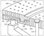
[0027]도 1은, 일 실시예에 따른 프로세싱 챔버(100)의 단면도이다. 프로세싱 챔버(100)는 챔버 본체(102) 및 제어기(106)를 포함한다. 챔버 본체(102)는 상부 돔(dome)(112), 링-형상 본체(160), 및 하부 돔(114)을 포함한다. 상부 돔(112) 및 하부 돔(114)은 링-형상 본체(160)를 샌드위칭하고(sandwich), 프로세싱 챔버(100)의 내부 용적(116)을 정의한다. 기판 지지 조립체(104)는 챔버 본체(102)의 내부 용적(116)에 포지셔닝된다.1 is a cross-sectional view of a
[0028]기판 지지 조립체(104)는 지지 샤프트 시스템(108), 서셉터(110), 및 열 플레이트(118)를 포함한다. 지지 샤프트 시스템(108)은 샤프트(120), 슈라우드(shroud; 122), 복수의 리프트 로드들(rods)(124), 복수의 아암들(126), 및 복수의 제거 가능한 지지 핀들(127)을 포함한다. 지지 샤프트 시스템(108)의 샤프트(120)는 슈라우드(122) 내에 포지셔닝된다. 액츄에이터(128)가 샤프트(120)에 커플링되고, 중심축에 대해 샤프트(120)를 회전시키도록 구성된다. 슈라우드(122)는 일반적으로 제 위치에 고정되고, 그러므로, 프로세싱동안 회전하지 않는다.[0028] The
[0029]복수의 아암들(126)은 샤프트(120)에 커플링된다. 아암들(126)은, 열 플레이트(118) 및 서셉터(110)를 지지하기 위해 방사상으로 밖을 향해(out) 연장된다. 각각의 아암(126)은 제 1 단부(130) 및 제 2 단부(132)를 갖는다. 각각의 아암(126)의 제 1 단부(130)는 샤프트(120)에 커플링된다. 각각의 아암(126)의 제 2 단부(132)는, 베이스 부재(134), 및 베이스 부재에 형성된 핀 수용 리세스(도 4a-4b; 7a-7b에 도시됨)를 포함한다. 핀 수용 리세스는 지지 핀(127)을 수용하도록 구성된다. 핀 수용 리세스는, 하나의 크기를 갖는 핀(127)이, 다른 크기를 갖는 핀(127)으로 교체되는 것을 허용한다. 예컨대, 하나의 길이를 갖는 핀(127)은, 다른 길이를 갖는 핀(127)으로 교체될 수 있다. 각각의 아암(126)은 열 플레이트(118)를 지지하도록 구성된다. 예컨대, 지지 샤프트 시스템(108)은, 개략적으로 120도 떨어져 균등하게 이격된 3개의 아암들(126)을 포함할 수 있다. 3개의 접촉점들이, 서셉터(110)를 지지하는 것을 돕는다.[0029] A plurality of
[0030]지지 핀들(127)은 열 플레이트(118)를 통해 연장되어 서셉터(110)를 지지한다. 서셉터(110)는, 서셉터(110)와 열 플레이트(118) 사이에 갭(136)이 정의되도록, 열 플레이트(118) 위에서 지지된다. 퍼지 가스 소스(138)로부터의 퍼지 가스는 갭(136)을 통해 유동할 수 있다. 퍼지 가스는, 서셉터(110) 아래를 지나가는 프로세스 가스에 기인한, 재료의 증착물(deposit)로부터의 기판(101)의 후면 변색을 감소시키는 것을 돕는다. 기판(101)은 열 플레이트(118) 바로 위에서 지지되며, 이에 의해, 열 플레이트(118)와 기판(101) 사이에 제 2 갭(140)이 형성된다. 기판(101)과 열 플레이트(118) 사이의 제 2 갭(140)은, 서셉터(110)와 열 플레이트(118) 사이에 형성된 갭(136)과 동일한 폭일 수 있다. 제 2 갭(140)은, 프로세스 가스가, 기판(101) 아래에서, 기판(101)과 열 플레이트(118) 사이에서 유동하는 것을 허용한다.[0030] The support pins 127 extend through the
[0031]리프트 로드들(124)은, 지지 샤프트 시스템(108)에 형성된 개구부들(도시되지 않음)을 통해 배치된다. 리프트 로드들(124)은 수직으로 액츄에이팅 가능(actuable)하다. 리프트 로드들(124)은, 기판(101)의 하측(142)과 접촉하여 (도시된 바와 같은) 프로세싱 포지션으로부터 기판 제거 포지션으로 기판(101)을 리프팅하도록 이루어진다.[0031] The
[0032]링-형상 본체(160)는, 링-형상 본체에 형성된 복수의 포트들을 포함한다. 예컨대, 유입구(148A)는, 프로세스 가스 소스(150)로부터 내부 용적(116) 내로 프로세스 가스를 제공하도록 이루어질 수 있다. 출구 포트(148B)는, 기판(101)에 걸친 프로세스 가스의 크로스 플로우(cross flow)를 유도하기 위해, 유입구(148A)의 맞은 편에 배치된다. 그러한 방식에서, 프로세스 가스는 기판(101)의 상부 표면에 대해 평행하게 유동할 수 있다. 열 소스(144)는, 기판(101) 상에 에피택셜 층(도시되지 않음)을 형성하기 위해, 기판(101) 상으로의 프로세스 가스의 열 분해(thermal decomposition)를 용이하게 한다.[0032] The ring-shaped
[0033]링-형상 본체(160)는 예열(preheat) 링(146)을 더 포함할 수 있다. 예열 링(146)은 챔버 본체(102)의 내부 용적(116) 주위에 배치되고, 기판(101)이 프로세싱 포지션에 있는 동안 기판(101)을 에워싼다(circumscribe). 프로세싱 동안, 예열 링(146)은 열 소스(144)에 의해 가열된다. 예열 링(146)은, 프로세스 가스가, 예열 링(146)에 인접한 유입구(148A)를 통해 링-형상 본체(160)에 진입할 때 프로세스 가스의 예열을 용이하게 한다.[0033] The ring-shaped
[0034]열 소스들(144)은, 예컨대, 프로세싱 챔버(100) 내에 포지셔닝된 컴포넌트들에 열 에너지를 제공하도록 이루어진 램프들일 수 있다. 예컨대, 열 소스(144)는, 기판(101), 서셉터(110), 및/또는 예열 링(146)에 열 에너지를 제공하도록 이루어질 수 있다. 하부 돔(114)은, 하부 돔을 통한 열 복사(thermal radiation)의 통과를 용이하게 하기 위해, 광학적으로 투명한 재료, 예컨대, 석영으로 형성될 수 있다. 일 실시예에서, 열 소스(144)는, 하부 돔(114) 뿐만 아니라 상부 돔(112)을 통해서도 열 에너지를 제공하도록 포지셔닝될 수 있다.[0034] The
[0035]고온계(152)는 기판(101) 및/또는 서셉터(110)의 온도를 측정하도록 이루어진다. 고온계(152)의 초점 빔(focal beam)(도시되지 않음)은 하부 돔(114)을 통해 그리고 샤프트(120)를 통해 지향된다. 고온계(152)는 서셉터(110)의 온도(예컨대, 서셉터(110)가 실리콘 카바이드로 형성된 경우), 또는 기판(101)의 온도(예컨대, 서셉터(110)가 석영으로 형성된 경우 또는 서셉터(110)가 없고 기판(101)이, 링에 의해서와 같이, 다른 방식으로 지지되는 경우)를 측정한다.[0035] The
[0036]프로세싱 챔버(100)는, 프로세싱 챔버(100)에서의 에피택셜 필름들의 성장과 같은 미리-결정된 프로세스들을 실행하고 모니터링하는 데에 사용되는 컴포넌트들을 포함한다. 프로세싱 챔버(100)는 하나 또는 그 초과의 가스 패널들, 가스 분배 도관들, 진공 및 배기 서브-시스템들, 전력 공급부들, 및 프로세스 제어 장비들을 포함한다. 제어기(106)는 프로세싱 챔버(100)에 커플링되고, 프로세싱 챔버(100)의 기능을 제어하도록 이루어진다.[0036] The
[0037]제어기(106)는, 프로세싱 챔버(100) 내에서의 기판(101)의 프로세싱을 제어하도록 동작 가능하다. 제어기(106)는, 기판(101)을 프로세싱하는 프로세스들의 제어를 용이하게 하기 위해, 프로세싱 챔버(100)의 다양한 컴포넌트들에 커플링된 프로그램 가능한 중앙 처리 장치(CPU)(154)를 포함하며, 프로그램 가능한 중앙 처리 장치는, 메모리(156) 및 대용량 저장 디바이스, 입력 제어 유닛, 및 디스플레이 유닛(도시되지 않음), 예컨대, 전력 공급부들, 클럭들, 캐시, 입력/출력(I/O) 회로들, 등과 함께 동작 가능하다. 제어기(106)는 또한, 프로세싱 챔버(100)의 센서들(도시되지 않음)을 통해 기판(101)의 프로세싱을 모니터링하기 위한 하드웨어를 포함할 수 있다.[0037] The
[0038]기판(101)을 프로세싱하는 것, 및 프로세싱 챔버(100)의 제어를 용이하게 하기 위해, CPU(154)는, 기판 프로세스를 제어하기 위한 임의의 형태의 범용 컴퓨터 프로세서들 중 하나일 수 있다. 메모리(156)는 CPU(154)에 커플링되고, 메모리(156)는 비-일시적(non-transitory)이며, 용이하게 입수 가능한 메모리, 예컨대, RAM(random access memory), ROM(read only memory), 플로피 디스크 드라이브, 하드 디스크, 또는 로컬 또는 원격의 임의의 다른 형태의 디지털 저장소 중 하나 또는 그 초과일 수 있다. 지원 회로들(158)은 통상적인 방식으로 CPU(154)를 지원하기 위해 CPU(154)에 커플링된다. 기판(101)을 프로세싱하기 위한 프로세스는 일반적으로, 메모리(156)에 저장된다. 기판(101)을 프로세싱하기 위한 프로세스는 또한, CPU(154)에 의해 제어되는 하드웨어로부터 원격으로 로케이팅된 제 2 CPU(도시되지 않음)에 의해서 저장되고 그리고/또는 실행될 수 있다.[0038] To facilitate processing the
[0039]메모리(156)는, 명령들을 포함하는 컴퓨터-판독 가능 저장 매체의 형태이며, 명령들은, CPU(154)에 의해 실행될 때, 프로세싱 챔버(100)에서 기판(101)을 프로세싱하는 동작을 용이하게 한다. 메모리(156)에 있는 명령들은, 기판(101)을 프로세싱하는 동작을 구현한 프로그램과 같은 프로그램 제품의 형태이다. 프로그램 코드는 다수의 상이한 프로그래밍 언어들 중 임의의 하나에 부합할 수 있다. 일 예에서, 본 개시물은, 컴퓨터 시스템과 함께 사용하기 위한 컴퓨터 판독 가능 저장 매체에 저장된 프로그램 제품으로 구현될 수 있다. 프로그램 제품의 프로그램(들)은 실시예들의 기능들을 정의한다. 예시적인 컴퓨터-판독 가능 저장 매체는: (i) 정보가 영구적으로 저장되는 기록-불가 저장 매체(예컨대, 컴퓨터 내의 읽기-전용 메모리 디바이스들, 예를 들어, CD-ROM 드라이브에 의해 판독 가능한 CD-ROM 디스크들, 플래시 메모리, ROM 칩들, 또는 임의의 유형의 솔리드-스테이트(solid-state) 비-휘발성 반도체 메모리); 및 (ii) 변경 가능한 정보가 저장되는 기록 저장 매체(예컨대, 하드-디스크 드라이브 또는 디스켓 드라이브 내의 플로피 디스크들 또는 임의의 유형의 솔리드-스테이트 랜덤-액세스 반도체 메모리)를 포함하지만, 이에 제한되지 않는다. 그러한 컴퓨터-판독 가능 저장 매체는, 본원에서 설명되는 방법들의 기능들을 지시하는 컴퓨터-판독 가능 명령들을 갖고(carrying) 있을 때, 본 개시물의 실시예들이다.[0039] The
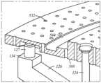
[0040]도 2a는 열 플레이트(118)의 측면도를 도시한다. 열 플레이트(118)는 제 1 디스크 형상 본체(200) 및 제 2 디스크 형상 본체(202)를 포함한다. 열 플레이트(118)는 탄소 그라파이트 또는 실리콘 그라파이트 코팅으로 만들어질 수 있다. 제 1 디스크 형상 본체(200)는 바닥부 표면(204), 정상부 표면(206), 내측 벽(208), 및 외측 벽(210)을 포함한다. 정상부 표면(206)은 바닥부 표면(204)에 대향하고, 바닥부 표면(204)에 대해서 평행하다. 내측 벽(208)은 바닥부 표면(204)에 대해 수직이고, 바닥부 표면(204)을 정상부 표면(206)에 연결한다. 내측 벽(208)은 내측 직경(212)을 포함한다. 외측 벽(210)은 내측 벽(208)에 대향하고, 정상부 표면(206)을 바닥부 표면(204)에 연결한다. 외측 벽(210)은, 외측 직경(214)이 내측 직경(212)보다 더 크도록 하는 외측 직경(214)을 포함한다.2A shows a side view of the
[0041]제 2 디스크 형상 본체(202)는 제 1 디스크 형상 본체(200)와 동심(concentric)이다. 제 2 디스크 형상 본체(202)는 바닥부 표면(216), 정상부 표면(218), 내측 벽(220), 및 외측 벽(222)을 포함한다. 정상부 표면(218)은 바닥부 표면(216)에 대향하고, 바닥부 표면(216)에 대해서 평행하다. 바닥부 표면(216)은 제 1 디스크 형상 본체(200)의 정상부 표면(206)에 커플링된다. 내측 벽(220)은 바닥부 표면(216)에 대해 수직이고, 바닥부 표면(216)을 정상부 표면(218)에 연결한다. 내측 벽(220)은, 내측 직경(224)이 제 1 디스크 형상 본체(200)의 내측 직경(212)보다 더 크도록 하는 내측 직경(224)을 갖는다. 외측 벽(222)은 내측 벽(220)에 대향하고, 내측 벽(220)에 대해 평행하다. 외측 벽(222)은 바닥부 표면(216)을 정상부 표면(218)에 연결한다. 외측 벽(222)은, 외측 직경(226)이 제 1 디스크 형상 본체(200)의 외측 직경(214)보다 더 작고 내측 직경(224)보다 더 크도록 하는 외측 직경(226)을 갖는다. 제 1 디스크 형상 본체(200) 및 제 2 디스크 형상 본체(202)는 제 1 디스크 형상 본체(200)의 정상부 표면(206)에서 레지(ledge; 228)를 정의한다.[0041] The second disc-shaped
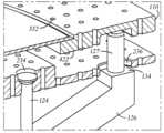
[0042]도 2b는, 열 플레이트(118)의 평면 사시도이다. 열 플레이트(118)는, 열 플레이트(118)를 관통하여 형성된 복수의 홀들(232, 234, 236)을 더 포함한다. 제 2 디스크 형상 본체(202)는 홀들(232, 234)의 2개의 세트들을 포함한다. 홀들(232, 234)의 세트들 양자 모두는, 제 2 디스크 형상 본체(202)의 정상부 표면(218)과 제 1 디스크 형상 본체(200)의 바닥부 표면(204) 사이의 유체 연통(fluid communication)을 제공한다. 홀들(232)의 제 1 세트는 홀들(234)의 제 2 세트보다 더 작은 직경을 갖는다. 열 플레이트(118)는 평방 센티미터 당 약 5.25개 홀들의 홀 밀도를 갖고, 퍼지 가스가 기판(도시되지 않음) 아래에서 유동되는 것을 허용한다. 홀들(234)의 제 2 세트는, 예컨대, 서로로부터 120도 떨어진 3개의 홀들과 같이, 제 2 디스크 형상 본체(202)의 둘레 주위에 균등하게 이격된다. 홀들(234)의 제 2 세트는, 지지 팁(도시되지 않음)이, 홀들(234)을 통해 연장될 수 있도록 그리고 기판을 서셉터(도시되지 않음)로부터 상승시키거나 서셉터 상으로 하강시킬 수 있도록 구성된다.2B is a top perspective view of the
[0043]홀들(236)의 제 3 세트는 열 플레이트(118)의 레지(228) 상에 배치된다. 홀들(236)의 제 3 세트는, 제 1 디스크 형상 본체(200)의 바닥부 표면(204)과 레지(228) 사이의 유체 연통을 제공한다. 홀들(236)의 제 3 세트는, 서셉터를 지지하기 위해 지지 핀들(도시되지 않음)이 홀들(236)을 통해서 연장될 수 있도록 구성된다. 홀들(236)의 제 3 세트는, 예컨대, 서로로부터 120도 떨어진 것과 같이, 레지(228)를 따라서 균등하게 이격될 수 있다.[0043] A third set of
[0044]도 3a는, 서셉터(110)의 부분의 측면 사시도이다. 서셉터(110)는 링 형상 본체(300)를 포함한다. 서셉터(110)는, 예컨대, 탄소 그라파이트와 같은, 열 플레이트(118)와 동일한 재료로 만들어질 수 있거나, 또는 서셉터(110)는 실리콘 그라파이트 코팅을 가질 수 있다. 링 형상 본체(300)는 바닥부 표면(302), 정상부 표면(304), 외측 벽(306), 내측 벽(308), 만입된(indented) 벽(310), 및 레지(312)를 포함한다. 바닥부 표면(302)은 제 1 길이(314)를 갖고, 정상부 표면(304)에 대향하며, 정상부 표면(304)에 대해 평행하다. 바닥부 표면(302)은, 도 4d에 도시된 바와 같이, 지지 핀의 정상부 표면과 접촉하도록 구성된다. 정상부 표면(304)은 제 2 길이(316)를 포함한다.[0044] FIG. 3A is a side perspective view of a portion of the
[0045]외측 벽(306)은 바닥부 표면(302)에 대해 수직이고, 제 1 높이(318) 및 외측 직경(320)을 포함한다. 외측 벽(306)은 정상부 표면(304)을 바닥부 표면(302)에 연결한다. 내측 벽(308)은 제 2 높이(322) 및 내측 직경(324)을 포함하며, 내측 직경(324)은 외측 직경(320)보다 더 작다. 외측 벽(306)은 바닥부 표면(302)에 대해 수직이다. 만입된 벽(310)은 바닥부 표면(302)에 대해 수직이고, 내측 직경(324)보다 더 크고 외측 직경(320)보다 더 작은 직경(326) 및 제 3 높이(328)를 포함한다. 만입된 벽(310)의 제 3 높이(328)는, 만입된 벽(310)의 제 3 높이(328)와 내측 벽(308)의 제 2 높이(322)를 더한 것이, 외측 벽(306)의 제 1 높이(318)와 실질적으로 동일하게 하는 높이이다.[0045] The
[0046]레지(312)는 내측 벽(308) 및 만입된 벽(310)에 의해 정의된다. 레지(312)는 바닥부 표면(302)에 대해 평행하며, 레지(312)의 길이(330)와 정상부 표면(304)의 제 2 길이(316)를 더한 것이, 바닥부 표면(302)의 제 1 길이(314)와 실질적으로 동일하게 하는 길이를 갖는다.[0046] The
[0047]도 3b는, 서셉터의 평면 사시도이다. 레지(312)는, 레지(312)를 관통하여 형성된 복수의 홀들(332)을 더 포함한다. 레지(312)의 복수의 홀들(332)은 바닥부 표면(302)과의 유체 연통을 제공한다. 레지(312)의 복수의 홀들(332)은, 퍼지 가스가, 열 플레이트 아래로부터 열 플레이트를 통해, 갭을 통해, 그리고 서셉터(110)를 통해 유동할 수 있도록, 열 플레이트(도시되지 않음)의 레지의 복수의 홀들(도시되지 않음)과 정렬된다. 서셉터(110)는 평방 센티미터 당 약 5.99개 홀들의 홀 밀도를 갖는다.[0047] Figure 3b is a plan perspective view of the susceptor. The
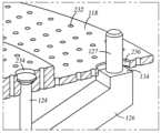
[0048]도 4a는, 지지 샤프트 시스템(108)의 아암(126)의 측면 사시도이다. 지지 샤프트 시스템(108)의 아암(126)은 2개의 단부들, 즉, 제 1 단부(도시되지 않음) 및 제 2 단부(132)를 포함한다. 제 2 단부(132)는, 핀 수용 리세스(400)가 형성된 베이스 부재(134)를 갖는다. 핀 수용 리세스(400)는, (도 4d에 도시된 바와 같이) 열 플레이트와 서셉터 사이의 갭이 변경될 수 있도록, (도 4b에 도시된 바와 같이) 교환 가능한 핀들을 수용하도록 구성된다. 핀 수용 리세스(400)는 또한, 서셉터를 지지하도록 구성된다. 베이스 부재(134)는 열 플레이트를 지지하도록 구성된다. 예컨대, 열 플레이트와 서셉터 사이의 갭은 적어도 0.1mm일 수 있으며, 예컨대, 0.1mm 내지 1mm범위일 수 있다.4A is a side perspective view of
[0049]도 4b는, 지지 핀(127)이 제 위치에 있는, 도 4a의 아암(126)의 측면 사시도이다. 지지 핀들(127)은 제 1 원통형 부분(404) 및 제 2 원통형 부분(406)을 포함한다. 핀들(127)은 SiC로 만들어질 수 있다. 제 1 원통형 부분(404)은 정상부 표면(408), 바닥부 표면(410), 내측 벽(412) 및 외측 벽(414)을 포함한다. 정상부 표면(408)은 바닥부 표면(410)에 대향하고, 바닥부 표면(410)에 대해서 평행하다. 내측 벽(412) 및 외측 벽(414)은 서로에 대해 평행하며, 바닥부 표면(410)에 대해 수직이다. 벽들(412, 414)은 정상부 표면(408)을 바닥부 표면(410)에 연결한다. 내측 벽(412)은 내측 직경(416)을 더 포함한다. 외측 벽(414)은 외측 직경(418)을 더 포함하며, 외측 직경(418)은 내측 직경(416)보다 더 크다.4B is a side perspective view of the
[0050]제 2 원통형 부분(406)은 정상부 표면(420), 바닥부 표면(422), 내측 벽(424) 및 외측 벽(426)을 포함한다. 정상부 표면(420)은 바닥부 표면(422)에 대향하고, 바닥부 표면(422)에 대해서 평행하다. 제 2 원통형 부분(406)의 바닥부 표면(422)은 제 1 원통형 부분(404)의 정상부 표면(420)에 커플링된다. 내측 벽(424)은 외측 벽(426)에 대해 평행하며, 벽들(424, 426) 양자 모두는 바닥부 표면(422)에 대해 수직이다. 벽들(424, 426)은 정상부 표면(420)을 바닥부 표면(422)에 연결한다. 내측 벽(424)은 내측 벽 직경(428)을 더 포함하며, 내측 벽 직경(428)은 제 1 원통형 부분(404)의 내측 직경(416)보다 더 작다. 외측 벽(426)은 외측 직경(430)을 더 포함하며, 외측 직경(430)은 제 1 원통형 부분(404)의 외측 직경(418)보다 더 크다.[0050] The second
[0051]도 4c는, 열 플레이트(118)가 제 위치에 있는, 도 4b의 아암(126)의 측면 사시도이다. 열 플레이트(118)는 지지 샤프트 시스템(108)에 의해 지지된다. 아암(126)의 베이스 부재(134)는 열 플레이트(118)와 접촉하고, 열 플레이트(118)를 지지한다. 복수의 핀들(127)은, 열 플레이트(118)에 형성된 홀들(234)을 통해 연장된다. 복수의 핀들(127)은 서셉터(도시되지 않음)를 지지하도록 구성된다.4C is a side perspective view of the
[0052]도 4d는, 서셉터(110)가 제 위치에 있는, 도 4c의 아암(126)의 측면 사시도이다. 서셉터(110)의 바닥부 표면(302)은, 서셉터(110)의 바닥부 표면(302)과 열 플레이트(118)의 정상부 표면들(206, 218) 사이에 갭(136)이 생성되도록, 지지 핀(127)의 제 2 원통형 부분(406)의 정상부 표면(420)에 의해 지지된다. 갭(136)은, 챔버(100)의 바닥부로부터 제공되는 퍼지 가스가, 프로세싱 동안 기판(101)의 아래로부터 흘러나오는 것을 허용하여, 프로세스 가스로부터의 기판의 후면 표면 상의 증착의 감소를 초래한다. 부가적으로, 열 플레이트(118)의 홀들(232)은, 열 플레이트(118) 및 서셉터(110)가 아암(126)에 의해 지지될 때, 서셉터(110)의 홀들(332)과 정렬된다. 홀 정렬은, 퍼지 가스가, 챔버(100)의 상부 돔(112)에 도달하는 것을 허용한다. 홀들(232, 332)은 또한, 수직 방향으로 상승하는 퍼지 가스와 수평 방향으로 기판의 표면에 걸쳐서 유동하는 프로세스 가스 사이의 난류를 감소시키는 기능을 한다. 홀들(232, 332)은, 퍼지 가스가 챔버(100)에서 상승하는 레이트(rate)를 늦추고, 이로 인해, 프로세스 가스를 만날 때 더 적은 난류를 야기한다. 난류의 감소는 또한, 기판 상에서의 재료의 더 매끄러운(smoother) 증착을 허용한다.4D is a side perspective view of the
[0053]도 5a는, 열 플레이트(500)의 다른 실시예의 측면 사시도이다. 열 플레이트(500)는 제 1 디스크 형상 본체(502) 및 제 2 디스크 형상 본체(504)를 포함한다. 제 1 디스크 형상 본체(502)는 바닥부 표면(506), 정상부 표면(508), 내측 벽(510), 및 외측 벽(512)을 포함한다. 정상부 표면(508)은 바닥부 표면(506)에 대향하고, 바닥부 표면(506)에 대해서 평행하다. 내측 벽(510)은 바닥부 표면(506)에 대해 수직이고, 바닥부 표면(506)을 정상부 표면(508)에 연결한다. 내측 벽(510)은 내측 직경(514)을 포함한다. 외측 벽(512)은 내측 벽(510)에 대향하고, 정상부 표면(508)을 바닥부 표면(506)에 연결한다. 외측 벽(512)은, 외측 직경(516)이 내측 직경(514)보다 더 크도록 하는 외측 직경(516)을 포함한다.5A is a side perspective view of another embodiment of a
[0054]정상부 표면(508)은 제 1 평면(536) 및 제 2 평면(538)을 더 포함한다. 제 1 평면(536)은 제 2 평면(538) 위에 안착된다. 제 2 평면(538)은, 바닥부 표면(506)에 대해 수직인 2개의 측벽들(540)을 포함한다. 2개의 측벽들(540)은 제 1 평면(536)을 제 2 평면(538)에 연결한다. 하부 벽(542)은 바닥부 표면(506)에 대해 평행하고, 2개의 측벽들(540)을 연결한다. 하부 벽(542)은 측벽들(540)에 대해 수직이다. 2개의 측벽들(540) 및 하부 벽 (542)은, 제 1 디스크 형상 본체(502)의 정상부 표면(508)에 그루브(544)를 정의한다. 그루브(544)는 (도 7d에 도시된 바와 같이) 서셉터의 부분을 수용하도록 구성된다.[0054] The
[0055]제 2 디스크 형상 본체(504)는 제 1 디스크 형상 본체(502)와 동심이다. 제 2 디스크 형상 본체(504)는 바닥부 표면(518), 정상부 표면(520), 내측 벽(522), 및 외측 벽(524)을 포함한다. 정상부 표면(520)은 바닥부 표면(518)에 대향하고, 바닥부 표면(518)에 대해서 평행하다. 바닥부 표면(518)은 제 1 디스크 형상 본체(502)의 정상부 표면(520)에 커플링된다. 내측 벽(522)은 바닥부 표면(518)에 대해 수직이고, 바닥부 표면(518)을 정상부 표면(520)에 연결한다. 내측 벽(522)은, 내측 직경(526)이 제 1 디스크 형상 본체(502)의 내측 직경(514)보다 더 크도록 하는 내측 직경(526)을 갖는다. 외측 벽(524)은 내측 벽(522)에 대향하고, 내측 벽(522)에 대해 평행하다. 외측 벽(524)은 바닥부 표면(518)을 정상부 표면(520)에 연결한다. 외측 벽(524)은, 외측 직경(528)이 제 1 디스크 형상 본체(502)의 외측 직경(516)보다 더 작고 내측 직경(526)보다 더 크도록 하는 외측 직경(528)을 갖는다. 제 1 디스크 형상 본체(502) 및 제 2 디스크 형상 본체(504)는 제 1 디스크 형상 본체(502)의 정상부 표면(508)에서 레지(530)를 정의한다.[0055] The second disk-shaped
[0056]도 5b는, 도 5a에 예시된 열 플레이트(500)의 저면 사시도를 예시한다. 레지(530)는, 레지(530)를 관통하여 형성된 제 1 복수의 홀들(532) 및 레지(530)를 관통하여 형성된 제 2 복수의 홀들(534)을 포함한다. 제 1 복수의 홀들(532)은, 제 1 디스크 형상 본체(502)의 정상부 표면(508)과 제 1 디스크 형상 본체(502)의 바닥부 표면(506) 사이의 유체 연통을 제공한다. 홀들(532)은 제 1 직경을 갖는다. 제 2 복수의 홀들(534)은, 제 1 디스크 형상 본체(502)의 정상부 표면(508)과 제 2 디스크 형상 본체(504)의 바닥부 표면(518) 사이의 유체 연통을 제공한다. 제 2 복수의 홀들(534)은 제 2 직경을 가지며, 제 2 직경은 제 1 직경보다 더 크다. 제 2 복수의 홀들(534)은, (도 7d에 도시된 바와 같이) 기판이 프로세싱 챔버의 내부 영역에 위치되거나 제거될 수 있도록 리프트 팁들을 수용하게 구성된다. 열 플레이트(500)는 평방 센티미터 당 약 5.25개 홀들의 홀 밀도를 갖는다.[0056] FIG. 5B illustrates a bottom perspective view of the
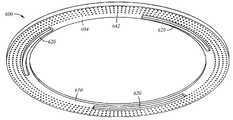
[0057]도 6a는, 서셉터(600)의 다른 실시예의 측면 사시도이다. 서셉터(600)는 디스크 형상 본체(602)를 포함한다. 디스크 형상 본체(602)는 바닥부 표면(604), 정상부 표면(606), 외측 벽(608), 내측 벽(610), 만입된 벽(612), 및 레지(614)를 포함한다. 정상부 표면(606)은 제 1 길이(616)를 포함한다. 바닥부 표면(604)은 제 2 길이(618)를 갖고, 정상부 표면(606)에 대향하며, 정상부 표면(606)에 대해 평행하다. 바닥부 표면(604)은, (도 7d에 도시된 바와 같이) 지지 팁의 정상부 표면과 접촉하도록 구성된다.[0057] FIG. 6A is a side perspective view of another embodiment of a
[0058]바닥부 표면(604)은, 바닥부 표면(604)에 커플링된 복수의 핀들(620)을 더 포함한다. 핀들(620)은 서셉터(600)의 바닥부 표면(604) 아래로 연장되며, 2개의 측벽들(622) 및 바닥부 표면(624)을 갖는다. 핀들(620)의 바닥부 표면들(624)은 서셉터(600)의 바닥부 표면(604)에 대향하며, 바닥부 표면(604)에 대해 평행하다. 2개의 측벽들(622)은 바닥부 표면(624)에 대해 수직이고, 서셉터(600)의 바닥부 표면(604)을 핀(620)의 바닥부 표면(624)에 연결한다. 핀들(620)은 (도 7d에 도시된 바와 같이) 열 플레이트의 그루브 내에 안착되도록 구성된다. 복수의 핀들(620)은 열 플레이트 및 서셉터와 동심이다. 핀들(620)은, 서셉터(600)의 바닥부 표면(604)과 열 플레이트의 정상부 표면 사이에 갭이 존재하도록, 서셉터(600)를 지지한다. 갭은, 원치 않는 증착에 의해 기판의 후면이 변색되지 않도록, 퍼지 가스가, 기판 아래로부터 흘러나오는 것을 허용한다.[0058] The
[0059]외측 벽(608)은 제 1 높이(628), 외측 직경(630)을 포함하고, 바닥부 표면(604)에 대해 수직이다. 외측 벽(608)은 정상부 표면(606)을 바닥부 표면(604)에 연결한다. 내측 벽(610)은 제 2 높이(632), 내측 직경(634)을 포함하며, 내측 직경(634)은 외측 직경(630)보다 더 작다. 외측 벽(608)은 바닥부 표면(604)에 대해 수직이다. 만입된 벽(612)은 바닥부 표면(604)에 대해 수직이고, 내측 직경(634)보다 더 크고 외측 직경(630)보다 더 작은 직경(638) 및 높이(636)를 포함한다. 만입된 벽(612)의 높이(636)는, 만입된 벽(612)의 높이(636)와 내측 벽(610)의 높이(632)를 더한 것이, 외측 벽(608)의 제 1 높이(628)와 실질적으로 동일하게 하는 높이이다.[0059] The
[0060]레지(614)는 내측 벽(610) 및 만입된 벽(612)에 의해 정의된다. 레지(614)는 바닥부 표면(604)에 대해 평행하며, 레지(614)의 길이(640)와 정상부 표면(606)의 제 1 길이(616)를 더한 것이, 바닥부 표면(604)의 제 2 길이(618)와 실질적으로 동일하게 하는 길이(640)를 갖는다.[0060] The
[0061]도 6b는, 도 6a의 서셉터의 저면 사시도를 예시한다. 레지(614)는, 레지(614)를 관통하여 형성된 복수의 홀들(642)을 더 포함한다. 레지(614)의 복수의 홀들(642)은 바닥부 표면(604)과의 유체 연통을 제공한다. 레지(614)의 복수의 홀들(642)은, 퍼지 가스가, 열 플레이트 아래로부터 열 플레이트를 통해, 갭을 통해, 그리고 서셉터(600)를 통해 유동할 수 있도록, 열 플레이트의 레지의 복수의 홀들과 정렬된다. 서셉터(600)는 평방 센티미터 당 약 6.06개 홀들의 홀 밀도를 갖는다.[0061] FIG. 6B illustrates a bottom perspective view of the susceptor of FIG. 6A. The
[0062]도 7a는, 지지 샤프트 시스템(108)의 아암(126)의 측면 사시도이다. 지지 샤프트 시스템(108)의 아암(126)은 2개의 단부들, 즉, 제 1 단부(130)(도시되지 않음) 및 제 2 단부(132)를 포함한다. 제 2 단부(132)는 베이스 부재(134), 및 베이스 부재 내에 형성된 핀 수용 리세스(400)를 포함한다. 핀(127)은, 지지 샤프트 시스템(108)의 높이가 변화될 수 있도록 변경될 수 있으며, 이는 결과적으로, (도 7d에 도시된 바와 같이) 갭(702)에 걸친 거리를 설정한다.7A is a side perspective view of
[0063]도 7b는, 지지 핀(127)이 제 위치에 있는, 도 7a의 아암(126)의 측면 사시도이다. 제 2 원통형 부분(406)이 핀 수용 리세스(400) 내에 포지셔닝될 때, 지지 핀(127)은 제 위치에 있다. 지지 핀(127)의 제 2 원통형 부분(406)의 바닥부 표면(422)은, 지지 핀(127)이 제 위치에 있을 때, 아암(126)의 베이스 부재(134)와 접촉한다.7B is a side perspective view of the
[0064]도 7c는, 열 플레이트(500)가 제 위치에 있는, 도 7b의 아암(126)의 측면 사시도이다. 핀(127)의 정상부 표면(520)은 열 플레이트(500)의 바닥부 표면(506)과 접촉하며, 이로써 핀들(127)은 열 플레이트(500)를 지지한다. 핀들(127)은, 예컨대, 3개의 핀들(127)이 120도 떨어져 배치된 것과 같이, 열 플레이트(500) 주위에 균등하게 배치된다.7C is a side perspective view of the
[0065]도 7d는, 서셉터(600)가 제 위치에 있는, 도 7c의 아암(126)의 측면 사시도이다. 서셉터(600)는, 서셉터(600)의 핀들(620)이 열 플레이트(500)의 그루브(544) 내에 놓이도록, 열 플레이트(500)의 정상에 배치된다. 핀들(620)은, 서셉터(600)와 열 플레이트(500) 사이에 갭(702)이 형성되도록 하는 높이(700)를 갖는다. 갭(702)은, 퍼지 가스가, 프로세싱 동안 기판(도시되지 않음) 아래로부터 흘러나오는 것을 허용하여, 원치 않는 증착된 재료로부터의 기판의 후면 변색의 감소를 초래한다. 부가적으로, 열 플레이트(500)의 홀들(532)은, 열 플레이트(500) 및 서셉터(600)가 아암(126)에 의해 지지될 때, 서셉터(600)의 홀들(642)과 정렬된다. 홀 정렬은, 퍼지 가스가, 챔버의 상부 돔에 도달하는 것을 허용한다. 홀들(532, 642)은 또한, 수직 방향으로 상승하는 퍼지 가스와 수평 방향으로 기판의 표면에 걸쳐서 유동하는 프로세스 가스 사이의 난류를 제한하는 방식으로 기능한다. 홀들(532, 642)은, 가스들 사이에서의 난류가 감소될 수 있도록, 퍼지 가스가 챔버에서 상승하는 레이트를 늦춘다. 난류의 감소는, 기판(101)의 상부 표면 상에서의 더 균일한 증착을 허용한다.7D is a side perspective view of the
[0066]전술한 내용은 본 개시물의 실시예들에 관한 것이지만, 본 개시물의 다른 그리고 추가적인 실시예들은 본 개시물의 기본적인 범위로부터 벗어나지 않고 안출될 수 있으며, 본 개시물의 범위는 이하의 청구항들에 의해서 결정된다.[0066] While the foregoing relates to embodiments of the present disclosure, other and additional embodiments of the present disclosure may be devised without departing from the basic scope of the present disclosure, which is covered by the following claims. It is decided.
Claims (15)
Translated fromKorean상기 프로세싱 챔버는,
내부 용적을 갖는 챔버 본체; 및
상기 내부 용적에 배치된 지지 샤프트 조립체(support shaft assembly)를 포함하고,
상기 지지 샤프트 조립체는,
지지 샤프트 시스템 ― 상기 지지 샤프트 시스템은,
샤프트;
복수의 아암들(arms) ― 각각의 아암은 제 1 단부 및 제 2 단부를 갖고, 각각의 아암의 상기 제 1 단부는 상기 샤프트에 커플링되며, 각각의 아암의 상기 제 2 단부는 핀 수용 리세스(pin receiving recess)를 가짐 ―; 및
복수의 제거 가능한 지지 핀들 ― 각각의 핀은 상기 핀 수용 리세스의 각각의 단부 내에 위치됨 ―을 포함함 ―;
상기 지지 샤프트 시스템에 의해 지지되는 디스크 형상 열 플레이트(heat plate) ― 상기 디스크 형상 열 플레이트는,
제 1 표면;
제 2 표면;
상기 제 1 표면 및 상기 제 2 표면에 대향하는 제 3 표면 ― 상기 제 1 표면은 상기 제 2 표면보다 수직 방향으로 더 아래에 있음 ―; 및
복수의 홀들 ― 상기 복수의 홀들의 각각의 홀은 상부 개구 및 하부 개구를 갖고, 상기 하부 개구는 상기 프로세싱 챔버의 내부 용적에 노출되며, 상기 복수의 홀들은 상기 디스크 형상 열 플레이트를 관통하여 형성되고, 복수의 홀들의 제 1 그룹은 상기 제 1 표면에서 상기 제 3 표면으로 연장되고, 복수의 홀의 제 2 그룹은 상기 제2 표면에서 상기 제3 표면으로 연장됨 ―을 포함함 ―; 및
링 형상 서셉터(susceptor)를 포함하며, 상기 링 형상 서셉터는, 상기 디스크 형상 열 플레이트와 상기 링 형상 서셉터 사이에 정의된 갭(gap)이 존재하도록 상기 지지 샤프트 시스템의 상기 복수의 제거 가능한 지지 핀들에 의해 지지되고, 상기 링 형상 서셉터는 내부에 형성된 복수의 서셉터 홀들을 가지며, 상기 복수의 서셉터 홀들은 상기 복수의 홀들의 제 1 그룹과 정렬되는,
반도체 프로세싱을 위한 프로세싱 챔버.A processing chamber for semiconductor processing,
The processing chamber,
a chamber body having an internal volume; and
a support shaft assembly disposed in the interior volume;
The support shaft assembly,
Support shaft system - the support shaft system comprises:
shaft;
a plurality of arms - each arm having a first end and a second end, the first end of each arm coupled to the shaft and the second end of each arm comprising a pin receiving ring; has a pin receiving recess; and
a plurality of removable support pins, each pin positioned within a respective end of the pin receiving recess;
A disk-shaped heat plate supported by the support shaft system - the disk-shaped heat plate comprising:
first surface;
second surface;
a third surface opposite to the first surface and the second surface, the first surface being lower than the second surface in a vertical direction; and
a plurality of holes - each hole of the plurality of holes has an upper opening and a lower opening, the lower opening being exposed to an internal volume of the processing chamber, the plurality of holes being formed through the disk-shaped thermal plate; , a first group of plurality of holes extends from the first surface to the third surface, and a second group of plurality of holes extends from the second surface to the third surface; and
a ring-shaped susceptor, the ring-shaped susceptor comprising the plurality of removable parts of the support shaft system such that there is a defined gap between the disk-shaped thermal plate and the ring-shaped susceptor; supported by support pins, the ring-shaped susceptor having a plurality of susceptor holes formed therein, the plurality of susceptor holes being aligned with the first group of the plurality of holes;
A processing chamber for semiconductor processing.
상기 복수의 아암들의 각각의 아암은 베이스 부재를 포함하고, 상기 베이스 부재는 상기 디스크 형상 열 플레이트를 지지하는,
반도체 프로세싱을 위한 프로세싱 챔버.According to claim 1,
each arm of the plurality of arms includes a base member, the base member supporting the disc-shaped thermal plate;
A processing chamber for semiconductor processing.
상기 프로세싱 챔버는,
내부 용적을 갖는 챔버 본체; 및
상기 내부 용적에 배치된 지지 샤프트 조립체를 포함하고,
상기 지지 샤프트 조립체는,
지지 샤프트 시스템 ― 상기 지지 샤프트 시스템은,
샤프트; 및
복수의 아암들 ― 각각의 아암은 제 1 단부 및 제 2 단부를 갖고, 각각의 아암의 상기 제 1 단부는 상기 샤프트에 커플링됨 ― 을 포함함 ―;
상기 지지 샤프트 시스템에 의해 지지되는 디스크 형상 열 플레이트 ― 정상부 표면을 갖는 상기 디스크 형상 열 플레이트는 복수의 그루브들(grooves)을 더 포함하고, 상기 디스크 형상 열 플레이트는,
제 1 표면;
제 2 표면;
상기 제 1 표면 및 상기 제 2 표면에 대향하는 제 3 표면 ― 상기 제 1 표면은 상기 제 2 표면보다 수직 방향으로 더 아래에 있음 ―; 및
복수의 홀들 ― 상기 복수의 홀들의 각각의 홀은 상부 개구 및 하부 개구를 갖고, 상기 하부 개구는 상기 프로세싱 챔버의 내부 용적에 노출되며, 상기 복수의 홀들은 상기 디스크 형상 열 플레이트를 관통하여 형성되고, 복수의 홀들의 제 1 그룹은 상기 제 1 표면에서 상기 제 3 표면으로 연장되고, 복수의 홀의 제 2 그룹은 상기 제2 표면에서 상기 제3 표면으로 연장됨 ―을 포함함 ―; 및
복수의 핀들을 갖는 링 형상 서셉터 ― 상기 핀들은, 상기 디스크 형상 열 플레이트와 상기 링 형상 서셉터 사이에 갭이 존재하도록, 상기 디스크 형상 열 플레이트의 복수의 그루브들 내에 배치되고, 상기 링 형상 서셉터는 내부에 형성된 복수의 서셉터 홀들을 가지며, 상기 복수의 서셉터 홀들은 상기 복수의 홀들의 제 1 그룹과 정렬됨 ― 를 포함하는,
반도체 프로세싱을 위한 프로세싱 챔버.A processing chamber for semiconductor processing,
The processing chamber,
a chamber body having an internal volume; and
a support shaft assembly disposed in the interior volume;
The support shaft assembly,
Support shaft system - the support shaft system comprises:
shaft; and
a plurality of arms, each arm having a first end and a second end, the first end of each arm being coupled to the shaft;
A disk-shaped thermal plate supported by the support shaft system, the disk-shaped thermal plate having a top surface further comprising a plurality of grooves, the disk-shaped thermal plate comprising:
first surface;
second surface;
a third surface opposite to the first surface and the second surface, the first surface being lower than the second surface in a vertical direction; and
a plurality of holes - each hole of the plurality of holes has an upper opening and a lower opening, the lower opening being exposed to an internal volume of the processing chamber, the plurality of holes being formed through the disk-shaped thermal plate; , a first group of plurality of holes extends from the first surface to the third surface, and a second group of plurality of holes extends from the second surface to the third surface; and
A ring-shaped susceptor having a plurality of pins - the pins are disposed in a plurality of grooves of the disc-shaped thermal plate such that a gap exists between the disc-shaped thermal plate and the ring-shaped susceptor, and the ring-shaped susceptor wherein the susceptor has a plurality of susceptor holes formed therein, the plurality of susceptor holes being aligned with the first group of the plurality of holes.
A processing chamber for semiconductor processing.
상기 디스크 형상 열 플레이트에 형성된 상기 복수의 홀들의 부분은 평방 센티미터 당 5.25개 홀들의 홀 밀도를 갖는,
반도체 프로세싱을 위한 프로세싱 챔버.According to claim 1 or 3,
wherein the portion of the plurality of holes formed in the disk-shaped thermal plate has a hole density of 5.25 holes per square centimeter;
A processing chamber for semiconductor processing.
상기 링 형상 서셉터에 형성된 상기 복수의 홀들은 평방 센티미터 당 5.99개 홀들의 홀 밀도를 갖는,
반도체 프로세싱을 위한 프로세싱 챔버.According to claim 1 or 3,
The plurality of holes formed in the ring-shaped susceptor have a hole density of 5.99 holes per square centimeter,
A processing chamber for semiconductor processing.
상기 디스크 형상 열 플레이트에 형성된 복수의 홀들의 부분은 평방 센티미터 당 5.25개 홀들의 홀 밀도를 갖는,
반도체 프로세싱을 위한 프로세싱 챔버.According to claim 7,
the portion of the plurality of holes formed in the disk-shaped thermal plate has a hole density of 5.25 holes per square centimeter;
A processing chamber for semiconductor processing.
상기 링 형상 서셉터에 형성된 상기 복수의 홀들은 평방 센티미터 당 6.06개 홀들의 홀 밀도를 갖는,
반도체 프로세싱을 위한 프로세싱 챔버.According to claim 1 or 3,
The plurality of holes formed in the ring-shaped susceptor have a hole density of 6.06 holes per square centimeter,
A processing chamber for semiconductor processing.
상기 디스크 형상 열 플레이트에 형성된 복수의 홀들의 부분은 평방 센티미터 당 5.25개 홀들의 홀 밀도를 갖는,
반도체 프로세싱을 위한 프로세싱 챔버.According to claim 9,
the portion of the plurality of holes formed in the disk-shaped thermal plate has a hole density of 5.25 holes per square centimeter;
A processing chamber for semiconductor processing.
상기 디스크 형상 열 플레이트와 상기 링 형상 서셉터 사이의 갭은 적어도 0.1mm인,
반도체 프로세싱을 위한 프로세싱 챔버.According to claim 1 or 3,
The gap between the disk-shaped thermal plate and the ring-shaped susceptor is at least 0.1 mm,
A processing chamber for semiconductor processing.
상기 링 형상 서셉터는 기판을 수용하도록 구성된 레지를 더 포함하는,
반도체 프로세싱을 위한 프로세싱 챔버.According to claim 1 or 3,
The ring-shaped susceptor further comprises a ledge configured to receive a substrate,
A processing chamber for semiconductor processing.
상기 방법은,
프로세스 가스를 상기 프로세싱 챔버 내에 유동시키는 단계 ― 상기 프로세싱 챔버는,
내부 용적을 갖는 챔버 본체; 및
상기 내부 용적에 배치된 지지 샤프트 조립체를 포함하고,
상기 지지 샤프트 조립체는,
지지 샤프트 시스템 ― 상기 지지 샤프트 시스템은,
샤프트;
복수의 아암들 ― 각각의 아암은 제 1 단부 및 제 2 단부를 갖고, 각각의 아암의 상기 제 1 단부는 상기 샤프트에 커플링되며, 각각의 아암의 상기 제 2 단부는 핀 수용 리세스를 가짐 ―; 및
복수의 제거 가능한 지지 핀들 ― 각각의 핀은 상기 핀 수용 리세스의 각각의 단부 내에 위치됨 ― 을 포함함 ―;
상기 지지 샤프트 시스템에 의해 지지되는 디스크 형상 열 플레이트 ― 정상부 표면을 갖는 상기 디스크 형상 열 플레이트는 복수의 그루브들을 더 포함하고, 상기 디스크 형상 열 플레이트는,
제 1 표면;
제 2 표면;
상기 제 1 표면 및 상기 제 2 표면에 대향하는 제 3 표면 ― 상기 제 1 표면은 상기 제 2 표면보다 수직 방향으로 더 아래에 있음 ―; 및
복수의 홀들 ― 상기 복수의 홀들의 각각의 홀은 상부 개구 및 하부 개구를 갖고, 상기 하부 개구는 상기 프로세싱 챔버의 내부 용적에 노출되며, 상기 복수의 홀들은 상기 디스크 형상 열 플레이트를 관통하여 형성되고, 복수의 홀들의 제 1 그룹은 상기 제 1 표면에서 상기 제 3 표면으로 연장되고, 복수의 홀의 제 2 그룹은 상기 제2 표면에서 상기 제3 표면으로 연장됨 ―을 포함함 ―; 및
링 형상 서셉터 ― 상기 링 형상 서셉터는, 상기 디스크 형상 열 플레이트와 상기 링 형상 서셉터 사이에 정의된 갭이 존재하도록 상기 지지 샤프트 시스템의 복수의 핀들에 의해 지지되고, 상기 링 형상 서셉터는 내부에 형성된 복수의 서셉터 홀들을 가지며, 상기 복수의 서셉터 홀들은 상기 복수의 홀들의 제 1 그룹과 정렬됨 ―를 포함함 ―; 및
상기 디스크 형상 열 플레이트와 상기 링 형상 서셉터 사이에 형성된 상기 갭을 통해, 상기 기판 아래로부터 퍼지 가스를 흘러나오게 하는 단계를 포함하는,
프로세싱 챔버에서 기판을 프로세싱하기 위한 방법.A method for processing a substrate in a processing chamber, comprising:
The method,
flowing a process gas into the processing chamber, the processing chamber comprising:
a chamber body having an internal volume; and
a support shaft assembly disposed in the interior volume;
The support shaft assembly,
Support shaft system - the support shaft system comprises:
shaft;
a plurality of arms - each arm having a first end and a second end, the first end of each arm coupled to the shaft, and the second end of each arm having a pin receiving recess -; and
a plurality of removable support pins, each pin positioned within a respective end of the pin receiving recess;
a disk-shaped thermal plate supported by the support shaft system, the disk-shaped thermal plate having a top surface further comprising a plurality of grooves, the disk-shaped thermal plate comprising:
first surface;
second surface;
a third surface opposite to the first surface and the second surface, the first surface being lower than the second surface in a vertical direction; and
a plurality of holes - each hole of the plurality of holes has an upper opening and a lower opening, the lower opening being exposed to an internal volume of the processing chamber, the plurality of holes being formed through the disk-shaped thermal plate; , a first group of plurality of holes extends from the first surface to the third surface, and a second group of plurality of holes extends from the second surface to the third surface; and
Ring-shaped susceptor - the ring-shaped susceptor is supported by a plurality of pins of the support shaft system so that there is a defined gap between the disk-shaped thermal plate and the ring-shaped susceptor, the ring-shaped susceptor comprising: having a plurality of susceptor holes formed therein, the plurality of susceptor holes being aligned with the first group of the plurality of holes; and
and flowing a purge gas from under the substrate through the gap formed between the disk-shaped thermal plate and the ring-shaped susceptor.
A method for processing a substrate in a processing chamber.
Applications Claiming Priority (3)
| Application Number | Priority Date | Filing Date | Title |
|---|---|---|---|
| US201562102375P | 2015-01-12 | 2015-01-12 | |
| US62/102,375 | 2015-01-12 | ||
| PCT/US2015/065056WO2016114877A1 (en) | 2015-01-12 | 2015-12-10 | Support assembly for substrate backside discoloration control |
Publications (2)
| Publication Number | Publication Date |
|---|---|
| KR20170105563A KR20170105563A (en) | 2017-09-19 |
| KR102506495B1true KR102506495B1 (en) | 2023-03-03 |
Family
ID=56368033
Family Applications (1)
| Application Number | Title | Priority Date | Filing Date |
|---|---|---|---|
| KR1020177022628AActiveKR102506495B1 (en) | 2015-01-12 | 2015-12-10 | Support assembly for board back side discoloration control |
Country Status (6)
| Country | Link |
|---|---|
| US (1) | US10704146B2 (en) |
| JP (1) | JP6752797B2 (en) |
| KR (1) | KR102506495B1 (en) |
| CN (1) | CN107112267B (en) |
| TW (1) | TWI679298B (en) |
| WO (1) | WO2016114877A1 (en) |
Families Citing this family (256)
| Publication number | Priority date | Publication date | Assignee | Title |
|---|---|---|---|---|
| US20130023129A1 (en) | 2011-07-20 | 2013-01-24 | Asm America, Inc. | Pressure transmitter for a semiconductor processing environment |
| US10714315B2 (en) | 2012-10-12 | 2020-07-14 | Asm Ip Holdings B.V. | Semiconductor reaction chamber showerhead |
| US20160376700A1 (en) | 2013-02-01 | 2016-12-29 | Asm Ip Holding B.V. | System for treatment of deposition reactor |
| WO2015179081A1 (en) | 2014-05-21 | 2015-11-26 | Applied Materials, Inc. | Thermal processing susceptor |
| US10941490B2 (en) | 2014-10-07 | 2021-03-09 | Asm Ip Holding B.V. | Multiple temperature range susceptor, assembly, reactor and system including the susceptor, and methods of using the same |
| US10276355B2 (en) | 2015-03-12 | 2019-04-30 | Asm Ip Holding B.V. | Multi-zone reactor, system including the reactor, and method of using the same |
| US10458018B2 (en) | 2015-06-26 | 2019-10-29 | Asm Ip Holding B.V. | Structures including metal carbide material, devices including the structures, and methods of forming same |
| US10211308B2 (en) | 2015-10-21 | 2019-02-19 | Asm Ip Holding B.V. | NbMC layers |
| US11139308B2 (en) | 2015-12-29 | 2021-10-05 | Asm Ip Holding B.V. | Atomic layer deposition of III-V compounds to form V-NAND devices |
| US10529554B2 (en) | 2016-02-19 | 2020-01-07 | Asm Ip Holding B.V. | Method for forming silicon nitride film selectively on sidewalls or flat surfaces of trenches |
| US10343920B2 (en) | 2016-03-18 | 2019-07-09 | Asm Ip Holding B.V. | Aligned carbon nanotubes |
| US11453943B2 (en) | 2016-05-25 | 2022-09-27 | Asm Ip Holding B.V. | Method for forming carbon-containing silicon/metal oxide or nitride film by ALD using silicon precursor and hydrocarbon precursor |
| US9859151B1 (en) | 2016-07-08 | 2018-01-02 | Asm Ip Holding B.V. | Selective film deposition method to form air gaps |
| US10612137B2 (en) | 2016-07-08 | 2020-04-07 | Asm Ip Holdings B.V. | Organic reactants for atomic layer deposition |
| US9887082B1 (en) | 2016-07-28 | 2018-02-06 | Asm Ip Holding B.V. | Method and apparatus for filling a gap |
| US9812320B1 (en) | 2016-07-28 | 2017-11-07 | Asm Ip Holding B.V. | Method and apparatus for filling a gap |
| US11532757B2 (en) | 2016-10-27 | 2022-12-20 | Asm Ip Holding B.V. | Deposition of charge trapping layers |
| US10714350B2 (en) | 2016-11-01 | 2020-07-14 | ASM IP Holdings, B.V. | Methods for forming a transition metal niobium nitride film on a substrate by atomic layer deposition and related semiconductor device structures |
| KR102546317B1 (en) | 2016-11-15 | 2023-06-21 | 에이에스엠 아이피 홀딩 비.브이. | Gas supply unit and substrate processing apparatus including the same |
| KR102762543B1 (en) | 2016-12-14 | 2025-02-05 | 에이에스엠 아이피 홀딩 비.브이. | Substrate processing apparatus |
| US11447861B2 (en) | 2016-12-15 | 2022-09-20 | Asm Ip Holding B.V. | Sequential infiltration synthesis apparatus and a method of forming a patterned structure |
| US11581186B2 (en) | 2016-12-15 | 2023-02-14 | Asm Ip Holding B.V. | Sequential infiltration synthesis apparatus |
| US10269558B2 (en) | 2016-12-22 | 2019-04-23 | Asm Ip Holding B.V. | Method of forming a structure on a substrate |
| US11390950B2 (en) | 2017-01-10 | 2022-07-19 | Asm Ip Holding B.V. | Reactor system and method to reduce residue buildup during a film deposition process |
| US10468261B2 (en) | 2017-02-15 | 2019-11-05 | Asm Ip Holding B.V. | Methods for forming a metallic film on a substrate by cyclical deposition and related semiconductor device structures |
| US10770286B2 (en) | 2017-05-08 | 2020-09-08 | Asm Ip Holdings B.V. | Methods for selectively forming a silicon nitride film on a substrate and related semiconductor device structures |
| US12040200B2 (en) | 2017-06-20 | 2024-07-16 | Asm Ip Holding B.V. | Semiconductor processing apparatus and methods for calibrating a semiconductor processing apparatus |
| US11306395B2 (en) | 2017-06-28 | 2022-04-19 | Asm Ip Holding B.V. | Methods for depositing a transition metal nitride film on a substrate by atomic layer deposition and related deposition apparatus |
| KR20190009245A (en) | 2017-07-18 | 2019-01-28 | 에이에스엠 아이피 홀딩 비.브이. | Methods for forming a semiconductor device structure and related semiconductor device structures |
| US11374112B2 (en) | 2017-07-19 | 2022-06-28 | Asm Ip Holding B.V. | Method for depositing a group IV semiconductor and related semiconductor device structures |
| US10590535B2 (en) | 2017-07-26 | 2020-03-17 | Asm Ip Holdings B.V. | Chemical treatment, deposition and/or infiltration apparatus and method for using the same |
| TWI815813B (en) | 2017-08-04 | 2023-09-21 | 荷蘭商Asm智慧財產控股公司 | Showerhead assembly for distributing a gas within a reaction chamber |
| US10770336B2 (en) | 2017-08-08 | 2020-09-08 | Asm Ip Holding B.V. | Substrate lift mechanism and reactor including same |
| US10692741B2 (en) | 2017-08-08 | 2020-06-23 | Asm Ip Holdings B.V. | Radiation shield |
| US11769682B2 (en) | 2017-08-09 | 2023-09-26 | Asm Ip Holding B.V. | Storage apparatus for storing cassettes for substrates and processing apparatus equipped therewith |
| US11830730B2 (en) | 2017-08-29 | 2023-11-28 | Asm Ip Holding B.V. | Layer forming method and apparatus |
| US11295980B2 (en) | 2017-08-30 | 2022-04-05 | Asm Ip Holding B.V. | Methods for depositing a molybdenum metal film over a dielectric surface of a substrate by a cyclical deposition process and related semiconductor device structures |
| US10658205B2 (en) | 2017-09-28 | 2020-05-19 | Asm Ip Holdings B.V. | Chemical dispensing apparatus and methods for dispensing a chemical to a reaction chamber |
| US10403504B2 (en) | 2017-10-05 | 2019-09-03 | Asm Ip Holding B.V. | Method for selectively depositing a metallic film on a substrate |
| US10923344B2 (en) | 2017-10-30 | 2021-02-16 | Asm Ip Holding B.V. | Methods for forming a semiconductor structure and related semiconductor structures |
| CN111344522B (en) | 2017-11-27 | 2022-04-12 | 阿斯莫Ip控股公司 | Including clean mini-environment device |
| WO2019103613A1 (en) | 2017-11-27 | 2019-05-31 | Asm Ip Holding B.V. | A storage device for storing wafer cassettes for use with a batch furnace |
| US10872771B2 (en) | 2018-01-16 | 2020-12-22 | Asm Ip Holding B. V. | Method for depositing a material film on a substrate within a reaction chamber by a cyclical deposition process and related device structures |
| TWI799494B (en) | 2018-01-19 | 2023-04-21 | 荷蘭商Asm 智慧財產控股公司 | Deposition method |
| KR102695659B1 (en) | 2018-01-19 | 2024-08-14 | 에이에스엠 아이피 홀딩 비.브이. | Method for depositing a gap filling layer by plasma assisted deposition |
| US11081345B2 (en) | 2018-02-06 | 2021-08-03 | Asm Ip Holding B.V. | Method of post-deposition treatment for silicon oxide film |
| US10755955B2 (en)* | 2018-02-12 | 2020-08-25 | Applied Materials, Inc. | Substrate transfer mechanism to reduce back-side substrate contact |
| US10896820B2 (en) | 2018-02-14 | 2021-01-19 | Asm Ip Holding B.V. | Method for depositing a ruthenium-containing film on a substrate by a cyclical deposition process |
| WO2019158960A1 (en) | 2018-02-14 | 2019-08-22 | Asm Ip Holding B.V. | A method for depositing a ruthenium-containing film on a substrate by a cyclical deposition process |
| US10731249B2 (en) | 2018-02-15 | 2020-08-04 | Asm Ip Holding B.V. | Method of forming a transition metal containing film on a substrate by a cyclical deposition process, a method for supplying a transition metal halide compound to a reaction chamber, and related vapor deposition apparatus |
| KR102636427B1 (en) | 2018-02-20 | 2024-02-13 | 에이에스엠 아이피 홀딩 비.브이. | Substrate processing method and apparatus |
| US10975470B2 (en) | 2018-02-23 | 2021-04-13 | Asm Ip Holding B.V. | Apparatus for detecting or monitoring for a chemical precursor in a high temperature environment |
| US11473195B2 (en) | 2018-03-01 | 2022-10-18 | Asm Ip Holding B.V. | Semiconductor processing apparatus and a method for processing a substrate |
| US11629406B2 (en) | 2018-03-09 | 2023-04-18 | Asm Ip Holding B.V. | Semiconductor processing apparatus comprising one or more pyrometers for measuring a temperature of a substrate during transfer of the substrate |
| KR102646467B1 (en) | 2018-03-27 | 2024-03-11 | 에이에스엠 아이피 홀딩 비.브이. | Method of forming an electrode on a substrate and a semiconductor device structure including an electrode |
| US11230766B2 (en) | 2018-03-29 | 2022-01-25 | Asm Ip Holding B.V. | Substrate processing apparatus and method |
| KR102600229B1 (en) | 2018-04-09 | 2023-11-10 | 에이에스엠 아이피 홀딩 비.브이. | Substrate supporting device, substrate processing apparatus including the same and substrate processing method |
| US12025484B2 (en) | 2018-05-08 | 2024-07-02 | Asm Ip Holding B.V. | Thin film forming method |
| TWI811348B (en) | 2018-05-08 | 2023-08-11 | 荷蘭商Asm 智慧財產控股公司 | Methods for depositing an oxide film on a substrate by a cyclical deposition process and related device structures |
| US12272527B2 (en) | 2018-05-09 | 2025-04-08 | Asm Ip Holding B.V. | Apparatus for use with hydrogen radicals and method of using same |
| KR102596988B1 (en) | 2018-05-28 | 2023-10-31 | 에이에스엠 아이피 홀딩 비.브이. | Method of processing a substrate and a device manufactured by the same |
| TWI840362B (en) | 2018-06-04 | 2024-05-01 | 荷蘭商Asm Ip私人控股有限公司 | Wafer handling chamber with moisture reduction |
| US11718913B2 (en) | 2018-06-04 | 2023-08-08 | Asm Ip Holding B.V. | Gas distribution system and reactor system including same |
| US11286562B2 (en) | 2018-06-08 | 2022-03-29 | Asm Ip Holding B.V. | Gas-phase chemical reactor and method of using same |
| US10797133B2 (en) | 2018-06-21 | 2020-10-06 | Asm Ip Holding B.V. | Method for depositing a phosphorus doped silicon arsenide film and related semiconductor device structures |
| KR102568797B1 (en) | 2018-06-21 | 2023-08-21 | 에이에스엠 아이피 홀딩 비.브이. | Substrate processing system |
| TWI873894B (en) | 2018-06-27 | 2025-02-21 | 荷蘭商Asm Ip私人控股有限公司 | Cyclic deposition methods for forming metal-containing material and films and structures including the metal-containing material |
| KR102854019B1 (en) | 2018-06-27 | 2025-09-02 | 에이에스엠 아이피 홀딩 비.브이. | Periodic deposition method for forming a metal-containing material and films and structures comprising the metal-containing material |
| US10612136B2 (en) | 2018-06-29 | 2020-04-07 | ASM IP Holding, B.V. | Temperature-controlled flange and reactor system including same |
| US10388513B1 (en) | 2018-07-03 | 2019-08-20 | Asm Ip Holding B.V. | Method for depositing silicon-free carbon-containing film as gap-fill layer by pulse plasma-assisted deposition |
| US10755922B2 (en) | 2018-07-03 | 2020-08-25 | Asm Ip Holding B.V. | Method for depositing silicon-free carbon-containing film as gap-fill layer by pulse plasma-assisted deposition |
| US11430674B2 (en) | 2018-08-22 | 2022-08-30 | Asm Ip Holding B.V. | Sensor array, apparatus for dispensing a vapor phase reactant to a reaction chamber and related methods |
| KR102707956B1 (en) | 2018-09-11 | 2024-09-19 | 에이에스엠 아이피 홀딩 비.브이. | Method for deposition of a thin film |
| US11024523B2 (en) | 2018-09-11 | 2021-06-01 | Asm Ip Holding B.V. | Substrate processing apparatus and method |
| CN110970344B (en) | 2018-10-01 | 2024-10-25 | Asmip控股有限公司 | Substrate holding apparatus, system comprising the same and method of using the same |
| US11232963B2 (en) | 2018-10-03 | 2022-01-25 | Asm Ip Holding B.V. | Substrate processing apparatus and method |
| KR102592699B1 (en) | 2018-10-08 | 2023-10-23 | 에이에스엠 아이피 홀딩 비.브이. | Substrate support unit and apparatuses for depositing thin film and processing the substrate including the same |
| KR102605121B1 (en) | 2018-10-19 | 2023-11-23 | 에이에스엠 아이피 홀딩 비.브이. | Substrate processing apparatus and substrate processing method |
| KR102546322B1 (en) | 2018-10-19 | 2023-06-21 | 에이에스엠 아이피 홀딩 비.브이. | Substrate processing apparatus and substrate processing method |
| US12378665B2 (en) | 2018-10-26 | 2025-08-05 | Asm Ip Holding B.V. | High temperature coatings for a preclean and etch apparatus and related methods |
| US11087997B2 (en) | 2018-10-31 | 2021-08-10 | Asm Ip Holding B.V. | Substrate processing apparatus for processing substrates |
| KR102748291B1 (en) | 2018-11-02 | 2024-12-31 | 에이에스엠 아이피 홀딩 비.브이. | Substrate support unit and substrate processing apparatus including the same |
| US11572620B2 (en) | 2018-11-06 | 2023-02-07 | Asm Ip Holding B.V. | Methods for selectively depositing an amorphous silicon film on a substrate |
| US10818758B2 (en) | 2018-11-16 | 2020-10-27 | Asm Ip Holding B.V. | Methods for forming a metal silicate film on a substrate in a reaction chamber and related semiconductor device structures |
| US12040199B2 (en) | 2018-11-28 | 2024-07-16 | Asm Ip Holding B.V. | Substrate processing apparatus for processing substrates |
| US11217444B2 (en) | 2018-11-30 | 2022-01-04 | Asm Ip Holding B.V. | Method for forming an ultraviolet radiation responsive metal oxide-containing film |
| KR102636428B1 (en) | 2018-12-04 | 2024-02-13 | 에이에스엠 아이피 홀딩 비.브이. | A method for cleaning a substrate processing apparatus |
| US11158513B2 (en) | 2018-12-13 | 2021-10-26 | Asm Ip Holding B.V. | Methods for forming a rhenium-containing film on a substrate by a cyclical deposition process and related semiconductor device structures |
| TWI874340B (en) | 2018-12-14 | 2025-03-01 | 荷蘭商Asm Ip私人控股有限公司 | Method of forming device structure, structure formed by the method and system for performing the method |
| TWI866480B (en) | 2019-01-17 | 2024-12-11 | 荷蘭商Asm Ip 私人控股有限公司 | Methods of forming a transition metal containing film on a substrate by a cyclical deposition process |
| KR102727227B1 (en) | 2019-01-22 | 2024-11-07 | 에이에스엠 아이피 홀딩 비.브이. | Semiconductor processing device |
| KR102626263B1 (en) | 2019-02-20 | 2024-01-16 | 에이에스엠 아이피 홀딩 비.브이. | Cyclical deposition method including treatment step and apparatus for same |
| TWI873122B (en) | 2019-02-20 | 2025-02-21 | 荷蘭商Asm Ip私人控股有限公司 | Method of filling a recess formed within a surface of a substrate, semiconductor structure formed according to the method, and semiconductor processing apparatus |
| TWI838458B (en) | 2019-02-20 | 2024-04-11 | 荷蘭商Asm Ip私人控股有限公司 | Apparatus and methods for plug fill deposition in 3-d nand applications |
| TWI845607B (en) | 2019-02-20 | 2024-06-21 | 荷蘭商Asm Ip私人控股有限公司 | Cyclical deposition method and apparatus for filling a recess formed within a substrate surface |
| TWI842826B (en) | 2019-02-22 | 2024-05-21 | 荷蘭商Asm Ip私人控股有限公司 | Substrate processing apparatus and method for processing substrate |
| KR102858005B1 (en) | 2019-03-08 | 2025-09-09 | 에이에스엠 아이피 홀딩 비.브이. | Method for Selective Deposition of Silicon Nitride Layer and Structure Including Selectively-Deposited Silicon Nitride Layer |
| US11742198B2 (en) | 2019-03-08 | 2023-08-29 | Asm Ip Holding B.V. | Structure including SiOCN layer and method of forming same |
| JP2020167398A (en) | 2019-03-28 | 2020-10-08 | エーエスエム・アイピー・ホールディング・ベー・フェー | Door openers and substrate processing equipment provided with door openers |
| KR102809999B1 (en) | 2019-04-01 | 2025-05-19 | 에이에스엠 아이피 홀딩 비.브이. | Method of manufacturing semiconductor device |
| KR20200123380A (en) | 2019-04-19 | 2020-10-29 | 에이에스엠 아이피 홀딩 비.브이. | Layer forming method and apparatus |
| KR20200125453A (en) | 2019-04-24 | 2020-11-04 | 에이에스엠 아이피 홀딩 비.브이. | Gas-phase reactor system and method of using same |
| US11289326B2 (en) | 2019-05-07 | 2022-03-29 | Asm Ip Holding B.V. | Method for reforming amorphous carbon polymer film |
| KR20200130121A (en) | 2019-05-07 | 2020-11-18 | 에이에스엠 아이피 홀딩 비.브이. | Chemical source vessel with dip tube |
| KR20200130652A (en) | 2019-05-10 | 2020-11-19 | 에이에스엠 아이피 홀딩 비.브이. | Method of depositing material onto a surface and structure formed according to the method |
| CN110042368B (en)* | 2019-05-14 | 2025-05-09 | 本源量子计算科技(合肥)股份有限公司 | A device for producing graphene heterojunction by chemical vapor deposition |
| JP7598201B2 (en) | 2019-05-16 | 2024-12-11 | エーエスエム・アイピー・ホールディング・ベー・フェー | Wafer boat handling apparatus, vertical batch furnace and method |
| JP7612342B2 (en) | 2019-05-16 | 2025-01-14 | エーエスエム・アイピー・ホールディング・ベー・フェー | Wafer boat handling apparatus, vertical batch furnace and method |
| USD947913S1 (en) | 2019-05-17 | 2022-04-05 | Asm Ip Holding B.V. | Susceptor shaft |
| USD975665S1 (en) | 2019-05-17 | 2023-01-17 | Asm Ip Holding B.V. | Susceptor shaft |
| KR20200141002A (en) | 2019-06-06 | 2020-12-17 | 에이에스엠 아이피 홀딩 비.브이. | Method of using a gas-phase reactor system including analyzing exhausted gas |
| KR20200141931A (en) | 2019-06-10 | 2020-12-21 | 에이에스엠 아이피 홀딩 비.브이. | Method for cleaning quartz epitaxial chambers |
| KR20200143254A (en) | 2019-06-11 | 2020-12-23 | 에이에스엠 아이피 홀딩 비.브이. | Method of forming an electronic structure using an reforming gas, system for performing the method, and structure formed using the method |
| USD944946S1 (en) | 2019-06-14 | 2022-03-01 | Asm Ip Holding B.V. | Shower plate |
| CN114026268A (en)* | 2019-06-25 | 2022-02-08 | 皮考逊公司 | Substrate backside protection |
| KR20210005515A (en) | 2019-07-03 | 2021-01-14 | 에이에스엠 아이피 홀딩 비.브이. | Temperature control assembly for substrate processing apparatus and method of using same |
| JP7499079B2 (en) | 2019-07-09 | 2024-06-13 | エーエスエム・アイピー・ホールディング・ベー・フェー | Plasma device using coaxial waveguide and substrate processing method |
| CN112216646A (en) | 2019-07-10 | 2021-01-12 | Asm Ip私人控股有限公司 | Substrate supporting assembly and substrate processing device comprising same |
| KR20210010307A (en) | 2019-07-16 | 2021-01-27 | 에이에스엠 아이피 홀딩 비.브이. | Substrate processing apparatus |
| KR20210010816A (en) | 2019-07-17 | 2021-01-28 | 에이에스엠 아이피 홀딩 비.브이. | Radical assist ignition plasma system and method |
| KR102860110B1 (en) | 2019-07-17 | 2025-09-16 | 에이에스엠 아이피 홀딩 비.브이. | Methods of forming silicon germanium structures |
| US11643724B2 (en) | 2019-07-18 | 2023-05-09 | Asm Ip Holding B.V. | Method of forming structures using a neutral beam |
| TWI839544B (en) | 2019-07-19 | 2024-04-21 | 荷蘭商Asm Ip私人控股有限公司 | Method of forming topology-controlled amorphous carbon polymer film |
| KR20210010817A (en) | 2019-07-19 | 2021-01-28 | 에이에스엠 아이피 홀딩 비.브이. | Method of Forming Topology-Controlled Amorphous Carbon Polymer Film |
| TWI851767B (en) | 2019-07-29 | 2024-08-11 | 荷蘭商Asm Ip私人控股有限公司 | Methods for selective deposition utilizing n-type dopants and/or alternative dopants to achieve high dopant incorporation |
| CN112309899A (en) | 2019-07-30 | 2021-02-02 | Asm Ip私人控股有限公司 | Substrate processing apparatus |
| US12169361B2 (en) | 2019-07-30 | 2024-12-17 | Asm Ip Holding B.V. | Substrate processing apparatus and method |
| CN112309900A (en) | 2019-07-30 | 2021-02-02 | Asm Ip私人控股有限公司 | Substrate processing apparatus |
| US11587814B2 (en) | 2019-07-31 | 2023-02-21 | Asm Ip Holding B.V. | Vertical batch furnace assembly |
| US11227782B2 (en) | 2019-07-31 | 2022-01-18 | Asm Ip Holding B.V. | Vertical batch furnace assembly |
| US11587815B2 (en) | 2019-07-31 | 2023-02-21 | Asm Ip Holding B.V. | Vertical batch furnace assembly |
| CN112323048B (en) | 2019-08-05 | 2024-02-09 | Asm Ip私人控股有限公司 | Liquid level sensor for chemical source container |
| CN112342526A (en) | 2019-08-09 | 2021-02-09 | Asm Ip私人控股有限公司 | Heater assembly including cooling device and method of using same |
| USD965044S1 (en) | 2019-08-19 | 2022-09-27 | Asm Ip Holding B.V. | Susceptor shaft |
| USD965524S1 (en) | 2019-08-19 | 2022-10-04 | Asm Ip Holding B.V. | Susceptor support |
| JP2021031769A (en) | 2019-08-21 | 2021-03-01 | エーエスエム アイピー ホールディング ビー.ブイ. | Production apparatus of mixed gas of film deposition raw material and film deposition apparatus |
| USD949319S1 (en)* | 2019-08-22 | 2022-04-19 | Asm Ip Holding B.V. | Exhaust duct |
| KR20210024423A (en) | 2019-08-22 | 2021-03-05 | 에이에스엠 아이피 홀딩 비.브이. | Method for forming a structure with a hole |
| USD979506S1 (en) | 2019-08-22 | 2023-02-28 | Asm Ip Holding B.V. | Insulator |
| USD940837S1 (en) | 2019-08-22 | 2022-01-11 | Asm Ip Holding B.V. | Electrode |
| KR20210024420A (en) | 2019-08-23 | 2021-03-05 | 에이에스엠 아이피 홀딩 비.브이. | Method for depositing silicon oxide film having improved quality by peald using bis(diethylamino)silane |
| US11286558B2 (en) | 2019-08-23 | 2022-03-29 | Asm Ip Holding B.V. | Methods for depositing a molybdenum nitride film on a surface of a substrate by a cyclical deposition process and related semiconductor device structures including a molybdenum nitride film |
| KR102806450B1 (en) | 2019-09-04 | 2025-05-12 | 에이에스엠 아이피 홀딩 비.브이. | Methods for selective deposition using a sacrificial capping layer |
| KR102733104B1 (en) | 2019-09-05 | 2024-11-22 | 에이에스엠 아이피 홀딩 비.브이. | Substrate processing apparatus |
| US11562901B2 (en) | 2019-09-25 | 2023-01-24 | Asm Ip Holding B.V. | Substrate processing method |
| CN112593212B (en) | 2019-10-02 | 2023-12-22 | Asm Ip私人控股有限公司 | Method for forming topologically selective silicon oxide film by cyclic plasma enhanced deposition process |
| KR20210042810A (en) | 2019-10-08 | 2021-04-20 | 에이에스엠 아이피 홀딩 비.브이. | Reactor system including a gas distribution assembly for use with activated species and method of using same |
| TW202128273A (en) | 2019-10-08 | 2021-08-01 | 荷蘭商Asm Ip私人控股有限公司 | Gas injection system, reactor system, and method of depositing material on surface of substratewithin reaction chamber |
| TWI846953B (en) | 2019-10-08 | 2024-07-01 | 荷蘭商Asm Ip私人控股有限公司 | Substrate processing device |
| TWI846966B (en) | 2019-10-10 | 2024-07-01 | 荷蘭商Asm Ip私人控股有限公司 | Method of forming a photoresist underlayer and structure including same |
| US12009241B2 (en) | 2019-10-14 | 2024-06-11 | Asm Ip Holding B.V. | Vertical batch furnace assembly with detector to detect cassette |
| TWI834919B (en) | 2019-10-16 | 2024-03-11 | 荷蘭商Asm Ip私人控股有限公司 | Method of topology-selective film formation of silicon oxide |
| US11637014B2 (en) | 2019-10-17 | 2023-04-25 | Asm Ip Holding B.V. | Methods for selective deposition of doped semiconductor material |
| KR102845724B1 (en) | 2019-10-21 | 2025-08-13 | 에이에스엠 아이피 홀딩 비.브이. | Apparatus and methods for selectively etching films |
| KR20210050453A (en) | 2019-10-25 | 2021-05-07 | 에이에스엠 아이피 홀딩 비.브이. | Methods for filling a gap feature on a substrate surface and related semiconductor structures |
| US11646205B2 (en) | 2019-10-29 | 2023-05-09 | Asm Ip Holding B.V. | Methods of selectively forming n-type doped material on a surface, systems for selectively forming n-type doped material, and structures formed using same |
| KR20210054983A (en) | 2019-11-05 | 2021-05-14 | 에이에스엠 아이피 홀딩 비.브이. | Structures with doped semiconductor layers and methods and systems for forming same |
| US11501968B2 (en) | 2019-11-15 | 2022-11-15 | Asm Ip Holding B.V. | Method for providing a semiconductor device with silicon filled gaps |
| KR102861314B1 (en) | 2019-11-20 | 2025-09-17 | 에이에스엠 아이피 홀딩 비.브이. | Method of depositing carbon-containing material on a surface of a substrate, structure formed using the method, and system for forming the structure |
| US11450529B2 (en) | 2019-11-26 | 2022-09-20 | Asm Ip Holding B.V. | Methods for selectively forming a target film on a substrate comprising a first dielectric surface and a second metallic surface |
| CN112951697B (en) | 2019-11-26 | 2025-07-29 | Asmip私人控股有限公司 | Substrate processing apparatus |
| CN112885692B (en) | 2019-11-29 | 2025-08-15 | Asmip私人控股有限公司 | Substrate processing apparatus |
| CN120432376A (en) | 2019-11-29 | 2025-08-05 | Asm Ip私人控股有限公司 | Substrate processing apparatus |
| JP7527928B2 (en) | 2019-12-02 | 2024-08-05 | エーエスエム・アイピー・ホールディング・ベー・フェー | Substrate processing apparatus and substrate processing method |
| KR20210070898A (en) | 2019-12-04 | 2021-06-15 | 에이에스엠 아이피 홀딩 비.브이. | Substrate processing apparatus |
| KR20210078405A (en) | 2019-12-17 | 2021-06-28 | 에이에스엠 아이피 홀딩 비.브이. | Method of forming vanadium nitride layer and structure including the vanadium nitride layer |
| KR20210080214A (en) | 2019-12-19 | 2021-06-30 | 에이에스엠 아이피 홀딩 비.브이. | Methods for filling a gap feature on a substrate and related semiconductor structures |
| JP7730637B2 (en) | 2020-01-06 | 2025-08-28 | エーエスエム・アイピー・ホールディング・ベー・フェー | Gas delivery assembly, components thereof, and reactor system including same |
| JP7636892B2 (en) | 2020-01-06 | 2025-02-27 | エーエスエム・アイピー・ホールディング・ベー・フェー | Channeled Lift Pins |
| US11993847B2 (en) | 2020-01-08 | 2024-05-28 | Asm Ip Holding B.V. | Injector |
| KR20210093163A (en) | 2020-01-16 | 2021-07-27 | 에이에스엠 아이피 홀딩 비.브이. | Method of forming high aspect ratio features |
| KR102675856B1 (en) | 2020-01-20 | 2024-06-17 | 에이에스엠 아이피 홀딩 비.브이. | Method of forming thin film and method of modifying surface of thin film |
| TWI889744B (en) | 2020-01-29 | 2025-07-11 | 荷蘭商Asm Ip私人控股有限公司 | Contaminant trap system, and baffle plate stack |
| TW202513845A (en) | 2020-02-03 | 2025-04-01 | 荷蘭商Asm Ip私人控股有限公司 | Semiconductor structures and methods for forming the same |
| KR20210100010A (en) | 2020-02-04 | 2021-08-13 | 에이에스엠 아이피 홀딩 비.브이. | Method and apparatus for transmittance measurements of large articles |
| US11776846B2 (en) | 2020-02-07 | 2023-10-03 | Asm Ip Holding B.V. | Methods for depositing gap filling fluids and related systems and devices |
| TW202146691A (en) | 2020-02-13 | 2021-12-16 | 荷蘭商Asm Ip私人控股有限公司 | Gas distribution assembly, shower plate assembly, and method of adjusting conductance of gas to reaction chamber |
| KR20210103956A (en) | 2020-02-13 | 2021-08-24 | 에이에스엠 아이피 홀딩 비.브이. | Substrate processing apparatus including light receiving device and calibration method of light receiving device |
| TWI855223B (en) | 2020-02-17 | 2024-09-11 | 荷蘭商Asm Ip私人控股有限公司 | Method for growing phosphorous-doped silicon layer |
| CN113410160A (en) | 2020-02-28 | 2021-09-17 | Asm Ip私人控股有限公司 | System specially used for cleaning parts |
| KR20210113043A (en) | 2020-03-04 | 2021-09-15 | 에이에스엠 아이피 홀딩 비.브이. | Alignment fixture for a reactor system |
| KR20210116240A (en) | 2020-03-11 | 2021-09-27 | 에이에스엠 아이피 홀딩 비.브이. | Substrate handling device with adjustable joints |
| US11876356B2 (en) | 2020-03-11 | 2024-01-16 | Asm Ip Holding B.V. | Lockout tagout assembly and system and method of using same |
| KR102775390B1 (en) | 2020-03-12 | 2025-02-28 | 에이에스엠 아이피 홀딩 비.브이. | Method for Fabricating Layer Structure Having Target Topological Profile |
| US12173404B2 (en) | 2020-03-17 | 2024-12-24 | Asm Ip Holding B.V. | Method of depositing epitaxial material, structure formed using the method, and system for performing the method |
| KR102755229B1 (en) | 2020-04-02 | 2025-01-14 | 에이에스엠 아이피 홀딩 비.브이. | Thin film forming method |
| TWI887376B (en) | 2020-04-03 | 2025-06-21 | 荷蘭商Asm Ip私人控股有限公司 | Method for manufacturing semiconductor device |
| TWI888525B (en) | 2020-04-08 | 2025-07-01 | 荷蘭商Asm Ip私人控股有限公司 | Apparatus and methods for selectively etching silcon oxide films |
| KR20210127620A (en) | 2020-04-13 | 2021-10-22 | 에이에스엠 아이피 홀딩 비.브이. | method of forming a nitrogen-containing carbon film and system for performing the method |
| KR20210128343A (en) | 2020-04-15 | 2021-10-26 | 에이에스엠 아이피 홀딩 비.브이. | Method of forming chromium nitride layer and structure including the chromium nitride layer |
| US11821078B2 (en) | 2020-04-15 | 2023-11-21 | Asm Ip Holding B.V. | Method for forming precoat film and method for forming silicon-containing film |
| US11996289B2 (en) | 2020-04-16 | 2024-05-28 | Asm Ip Holding B.V. | Methods of forming structures including silicon germanium and silicon layers, devices formed using the methods, and systems for performing the methods |
| KR20210130646A (en) | 2020-04-21 | 2021-11-01 | 에이에스엠 아이피 홀딩 비.브이. | Method for processing a substrate |
| KR20210132612A (en) | 2020-04-24 | 2021-11-04 | 에이에스엠 아이피 홀딩 비.브이. | Methods and apparatus for stabilizing vanadium compounds |
| KR20210132600A (en) | 2020-04-24 | 2021-11-04 | 에이에스엠 아이피 홀딩 비.브이. | Methods and systems for depositing a layer comprising vanadium, nitrogen, and a further element |
| KR102866804B1 (en) | 2020-04-24 | 2025-09-30 | 에이에스엠 아이피 홀딩 비.브이. | Vertical batch furnace assembly comprising a cooling gas supply |
| TW202208671A (en) | 2020-04-24 | 2022-03-01 | 荷蘭商Asm Ip私人控股有限公司 | Methods of forming structures including vanadium boride and vanadium phosphide layers |
| CN113555279A (en) | 2020-04-24 | 2021-10-26 | Asm Ip私人控股有限公司 | Methods of forming vanadium nitride-containing layers and structures comprising the same |
| KR102783898B1 (en) | 2020-04-29 | 2025-03-18 | 에이에스엠 아이피 홀딩 비.브이. | Solid source precursor vessel |
| KR20210134869A (en) | 2020-05-01 | 2021-11-11 | 에이에스엠 아이피 홀딩 비.브이. | Fast FOUP swapping with a FOUP handler |
| JP7726664B2 (en) | 2020-05-04 | 2025-08-20 | エーエスエム・アイピー・ホールディング・ベー・フェー | Substrate processing system for processing a substrate |
| KR20210137395A (en) | 2020-05-07 | 2021-11-17 | 에이에스엠 아이피 홀딩 비.브이. | Apparatus and methods for performing an in-situ etch of reaction chambers with fluorine-based radicals |
| KR102788543B1 (en) | 2020-05-13 | 2025-03-27 | 에이에스엠 아이피 홀딩 비.브이. | Laser alignment fixture for a reactor system |
| TW202146699A (en) | 2020-05-15 | 2021-12-16 | 荷蘭商Asm Ip私人控股有限公司 | Method of forming a silicon germanium layer, semiconductor structure, semiconductor device, method of forming a deposition layer, and deposition system |
| KR20210143653A (en) | 2020-05-19 | 2021-11-29 | 에이에스엠 아이피 홀딩 비.브이. | Substrate processing apparatus |
| KR102795476B1 (en) | 2020-05-21 | 2025-04-11 | 에이에스엠 아이피 홀딩 비.브이. | Structures including multiple carbon layers and methods of forming and using same |
| KR20210145079A (en) | 2020-05-21 | 2021-12-01 | 에이에스엠 아이피 홀딩 비.브이. | Flange and apparatus for processing substrates |
| TWI873343B (en) | 2020-05-22 | 2025-02-21 | 荷蘭商Asm Ip私人控股有限公司 | Reaction system for forming thin film on substrate |
| KR20210146802A (en) | 2020-05-26 | 2021-12-06 | 에이에스엠 아이피 홀딩 비.브이. | Method for depositing boron and gallium containing silicon germanium layers |
| TWI876048B (en) | 2020-05-29 | 2025-03-11 | 荷蘭商Asm Ip私人控股有限公司 | Substrate processing device |
| TW202212620A (en) | 2020-06-02 | 2022-04-01 | 荷蘭商Asm Ip私人控股有限公司 | Apparatus for processing substrate, method of forming film, and method of controlling apparatus for processing substrate |
| TW202208659A (en) | 2020-06-16 | 2022-03-01 | 荷蘭商Asm Ip私人控股有限公司 | Method for depositing boron containing silicon germanium layers |
| TW202218133A (en) | 2020-06-24 | 2022-05-01 | 荷蘭商Asm Ip私人控股有限公司 | Method for forming a layer provided with silicon |
| TWI873359B (en) | 2020-06-30 | 2025-02-21 | 荷蘭商Asm Ip私人控股有限公司 | Substrate processing method |
| US12431354B2 (en) | 2020-07-01 | 2025-09-30 | Asm Ip Holding B.V. | Silicon nitride and silicon oxide deposition methods using fluorine inhibitor |
| TW202202649A (en) | 2020-07-08 | 2022-01-16 | 荷蘭商Asm Ip私人控股有限公司 | Substrate processing method |
| KR20220010438A (en) | 2020-07-17 | 2022-01-25 | 에이에스엠 아이피 홀딩 비.브이. | Structures and methods for use in photolithography |
| KR20220011092A (en) | 2020-07-20 | 2022-01-27 | 에이에스엠 아이피 홀딩 비.브이. | Method and system for forming structures including transition metal layers |
| TWI878570B (en) | 2020-07-20 | 2025-04-01 | 荷蘭商Asm Ip私人控股有限公司 | Method and system for depositing molybdenum layers |
| US12322591B2 (en) | 2020-07-27 | 2025-06-03 | Asm Ip Holding B.V. | Thin film deposition process |
| KR20220021863A (en) | 2020-08-14 | 2022-02-22 | 에이에스엠 아이피 홀딩 비.브이. | Method for processing a substrate |
| US12040177B2 (en) | 2020-08-18 | 2024-07-16 | Asm Ip Holding B.V. | Methods for forming a laminate film by cyclical plasma-enhanced deposition processes |
| TW202228863A (en) | 2020-08-25 | 2022-08-01 | 荷蘭商Asm Ip私人控股有限公司 | Method for cleaning a substrate, method for selectively depositing, and reaction system |
| US11725280B2 (en) | 2020-08-26 | 2023-08-15 | Asm Ip Holding B.V. | Method for forming metal silicon oxide and metal silicon oxynitride layers |
| TW202229601A (en) | 2020-08-27 | 2022-08-01 | 荷蘭商Asm Ip私人控股有限公司 | Method of forming patterned structures, method of manipulating mechanical property, device structure, and substrate processing system |
| TW202217045A (en) | 2020-09-10 | 2022-05-01 | 荷蘭商Asm Ip私人控股有限公司 | Methods for depositing gap filing fluids and related systems and devices |
| USD990534S1 (en) | 2020-09-11 | 2023-06-27 | Asm Ip Holding B.V. | Weighted lift pin |
| KR20220036866A (en) | 2020-09-16 | 2022-03-23 | 에이에스엠 아이피 홀딩 비.브이. | Silicon oxide deposition method |
| USD1012873S1 (en) | 2020-09-24 | 2024-01-30 | Asm Ip Holding B.V. | Electrode for semiconductor processing apparatus |
| TWI889903B (en) | 2020-09-25 | 2025-07-11 | 荷蘭商Asm Ip私人控股有限公司 | Semiconductor processing method |
| US12009224B2 (en) | 2020-09-29 | 2024-06-11 | Asm Ip Holding B.V. | Apparatus and method for etching metal nitrides |
| KR20220045900A (en) | 2020-10-06 | 2022-04-13 | 에이에스엠 아이피 홀딩 비.브이. | Deposition method and an apparatus for depositing a silicon-containing material |
| CN114293174A (en) | 2020-10-07 | 2022-04-08 | Asm Ip私人控股有限公司 | Gas supply unit and substrate processing apparatus including the same |
| TW202229613A (en) | 2020-10-14 | 2022-08-01 | 荷蘭商Asm Ip私人控股有限公司 | Method of depositing material on stepped structure |
| TW202232565A (en) | 2020-10-15 | 2022-08-16 | 荷蘭商Asm Ip私人控股有限公司 | Method of manufacturing semiconductor device, and substrate treatment apparatus using ether-cat |
| TW202217037A (en) | 2020-10-22 | 2022-05-01 | 荷蘭商Asm Ip私人控股有限公司 | Method of depositing vanadium metal, structure, device and a deposition assembly |
| TW202223136A (en) | 2020-10-28 | 2022-06-16 | 荷蘭商Asm Ip私人控股有限公司 | Method for forming layer on substrate, and semiconductor processing system |
| TW202229620A (en) | 2020-11-12 | 2022-08-01 | 特文特大學 | Deposition system, method for controlling reaction condition, method for depositing |
| TW202229795A (en) | 2020-11-23 | 2022-08-01 | 荷蘭商Asm Ip私人控股有限公司 | A substrate processing apparatus with an injector |
| TW202235649A (en) | 2020-11-24 | 2022-09-16 | 荷蘭商Asm Ip私人控股有限公司 | Methods for filling a gap and related systems and devices |
| TW202235675A (en) | 2020-11-30 | 2022-09-16 | 荷蘭商Asm Ip私人控股有限公司 | Injector, and substrate processing apparatus |
| US12255053B2 (en) | 2020-12-10 | 2025-03-18 | Asm Ip Holding B.V. | Methods and systems for depositing a layer |
| TW202233884A (en) | 2020-12-14 | 2022-09-01 | 荷蘭商Asm Ip私人控股有限公司 | Method of forming structures for threshold voltage control |
| US11946137B2 (en) | 2020-12-16 | 2024-04-02 | Asm Ip Holding B.V. | Runout and wobble measurement fixtures |
| TW202232639A (en) | 2020-12-18 | 2022-08-16 | 荷蘭商Asm Ip私人控股有限公司 | Wafer processing apparatus with a rotatable table |
| TW202226899A (en) | 2020-12-22 | 2022-07-01 | 荷蘭商Asm Ip私人控股有限公司 | Plasma treatment device having matching box |
| TW202242184A (en) | 2020-12-22 | 2022-11-01 | 荷蘭商Asm Ip私人控股有限公司 | Precursor capsule, precursor vessel, vapor deposition assembly, and method of loading solid precursor into precursor vessel |
| TW202231903A (en) | 2020-12-22 | 2022-08-16 | 荷蘭商Asm Ip私人控股有限公司 | Transition metal deposition method, transition metal layer, and deposition assembly for depositing transition metal on substrate |
| USD980814S1 (en) | 2021-05-11 | 2023-03-14 | Asm Ip Holding B.V. | Gas distributor for substrate processing apparatus |
| USD981973S1 (en) | 2021-05-11 | 2023-03-28 | Asm Ip Holding B.V. | Reactor wall for substrate processing apparatus |
| USD1023959S1 (en) | 2021-05-11 | 2024-04-23 | Asm Ip Holding B.V. | Electrode for substrate processing apparatus |
| USD980813S1 (en) | 2021-05-11 | 2023-03-14 | Asm Ip Holding B.V. | Gas flow control plate for substrate processing apparatus |
| USD990441S1 (en) | 2021-09-07 | 2023-06-27 | Asm Ip Holding B.V. | Gas flow control plate |
| USD1060598S1 (en) | 2021-12-03 | 2025-02-04 | Asm Ip Holding B.V. | Split showerhead cover |
| US12002660B2 (en)* | 2022-02-15 | 2024-06-04 | Taiwan Semiconductor Manufacturing Company, Ltd. | Semiconductor manufacturing chamber with plasma/gas flow control device |
| KR102844316B1 (en)* | 2024-02-07 | 2025-08-08 | 주식회사 에스지에스코리아 | Pressure control device of twin process chamber |
Citations (2)
| Publication number | Priority date | Publication date | Assignee | Title |
|---|---|---|---|---|
| JP2012124476A (en)* | 2010-11-16 | 2012-06-28 | Shin Etsu Handotai Co Ltd | Vapor growth device and manufacturing method of epitaxial wafer |
| US20130025538A1 (en)* | 2011-07-27 | 2013-01-31 | Applied Materials, Inc. | Methods and apparatus for deposition processes |
Family Cites Families (14)
| Publication number | Priority date | Publication date | Assignee | Title |
|---|---|---|---|---|
| US4798165A (en)* | 1985-10-07 | 1989-01-17 | Epsilon | Apparatus for chemical vapor deposition using an axially symmetric gas flow |
| JP3090339B2 (en)* | 1990-03-19 | 2000-09-18 | 株式会社東芝 | Vapor growth apparatus and method |
| US6113702A (en)* | 1995-09-01 | 2000-09-05 | Asm America, Inc. | Wafer support system |
| JPH1179888A (en)* | 1997-09-01 | 1999-03-23 | Inotetsuku Kk | Vapor phase growing apparatus |
| US6296712B1 (en)* | 1997-12-02 | 2001-10-02 | Applied Materials, Inc. | Chemical vapor deposition hardware and process |
| US6096135A (en)* | 1998-07-21 | 2000-08-01 | Applied Materials, Inc. | Method and apparatus for reducing contamination of a substrate in a substrate processing system |
| JP4666473B2 (en)* | 2005-05-12 | 2011-04-06 | 大日本スクリーン製造株式会社 | Substrate heat treatment equipment |
| US20080220150A1 (en)* | 2007-03-05 | 2008-09-11 | Applied Materials, Inc. | Microbatch deposition chamber with radiant heating |
| US7964038B2 (en)* | 2008-10-02 | 2011-06-21 | Applied Materials, Inc. | Apparatus for improved azimuthal thermal uniformity of a substrate |
| JP5038381B2 (en)* | 2009-11-20 | 2012-10-03 | 株式会社東芝 | Susceptor and deposition system |
| US20110155058A1 (en)* | 2009-12-18 | 2011-06-30 | Applied Materials, Inc. | Substrate processing apparatus having a radiant cavity |
| US20120073503A1 (en)* | 2010-09-24 | 2012-03-29 | Juno Yu-Ting Huang | Processing systems and apparatuses having a shaft cover |
| KR101859344B1 (en)* | 2012-01-26 | 2018-05-18 | 어플라이드 머티어리얼스, 인코포레이티드 | Thermal processing chamber with top substrate support assembly |
| US9202727B2 (en)* | 2012-03-02 | 2015-12-01 | ASM IP Holding | Susceptor heater shim |
- 2015
- 2015-12-10KRKR1020177022628Apatent/KR102506495B1/enactiveActive
- 2015-12-10CNCN201580073204.0Apatent/CN107112267B/enactiveActive
- 2015-12-10WOPCT/US2015/065056patent/WO2016114877A1/ennot_activeCeased
- 2015-12-10JPJP2017536797Apatent/JP6752797B2/enactiveActive
- 2015-12-17USUS14/973,079patent/US10704146B2/enactiveActive
- 2016
- 2016-01-11TWTW105100687Apatent/TWI679298B/enactive
Patent Citations (2)
| Publication number | Priority date | Publication date | Assignee | Title |
|---|---|---|---|---|
| JP2012124476A (en)* | 2010-11-16 | 2012-06-28 | Shin Etsu Handotai Co Ltd | Vapor growth device and manufacturing method of epitaxial wafer |
| US20130025538A1 (en)* | 2011-07-27 | 2013-01-31 | Applied Materials, Inc. | Methods and apparatus for deposition processes |
Also Published As
| Publication number | Publication date |
|---|---|
| TWI679298B (en) | 2019-12-11 |
| US20160204005A1 (en) | 2016-07-14 |
| US10704146B2 (en) | 2020-07-07 |
| CN107112267A (en) | 2017-08-29 |
| CN107112267B (en) | 2020-09-22 |
| TW201636450A (en) | 2016-10-16 |
| JP2018504781A (en) | 2018-02-15 |
| KR20170105563A (en) | 2017-09-19 |
| JP6752797B2 (en) | 2020-09-09 |
| WO2016114877A1 (en) | 2016-07-21 |
Similar Documents
| Publication | Publication Date | Title |
|---|---|---|
| KR102506495B1 (en) | Support assembly for board back side discoloration control | |
| JP6368773B2 (en) | Flow control liner with spatially dispersed gas flow paths | |
| TWI673396B (en) | Atmospheric epitaxial deposition chamber | |
| US20160068996A1 (en) | Susceptor and pre-heat ring for thermal processing of substrates | |
| JP7175766B2 (en) | Susceptor support | |
| CN111952149A (en) | Coated liner assemblies for semiconductor processing chambers | |
| TW201724320A (en) | Diode laser for wafer heating in EPI processes | |
| TWI692825B (en) | Light pipe arrays for thermal chamber applications and thermal processes | |
| TWI853825B (en) | Multizone lamp control and individual lamp control in a lamphead | |
| KR20160024378A (en) | Absorbing reflector for semiconductor processing chamber | |
| US20130284097A1 (en) | Gas distribution module for insertion in lateral flow chambers | |
| JP2016145391A (en) | Vaporization apparatus, and film deposition apparatus | |
| KR20180046451A (en) | Apparatus for Processing Substrate | |
| JPS61219794A (en) | Heating apparatus for gas phase growth apparatus |
Legal Events
| Date | Code | Title | Description |
|---|---|---|---|
| PA0105 | International application | Patent event date:20170811 Patent event code:PA01051R01D Comment text:International Patent Application | |
| PG1501 | Laying open of application | ||
| PA0201 | Request for examination | Patent event code:PA02012R01D Patent event date:20201119 Comment text:Request for Examination of Application | |
| E902 | Notification of reason for refusal | ||
| PE0902 | Notice of grounds for rejection | Comment text:Notification of reason for refusal Patent event date:20220416 Patent event code:PE09021S01D | |
| E701 | Decision to grant or registration of patent right | ||
| PE0701 | Decision of registration | Patent event code:PE07011S01D Comment text:Decision to Grant Registration Patent event date:20221207 | |
| PR0701 | Registration of establishment | Comment text:Registration of Establishment Patent event date:20230228 Patent event code:PR07011E01D | |
| PR1002 | Payment of registration fee | Payment date:20230228 End annual number:3 Start annual number:1 | |
| PG1601 | Publication of registration |