KR102501935B1 - Antenna device and electronic device comprising the same - Google Patents
Antenna device and electronic device comprising the sameDownload PDFInfo
- Publication number
- KR102501935B1 KR102501935B1KR1020160111337AKR20160111337AKR102501935B1KR 102501935 B1KR102501935 B1KR 102501935B1KR 1020160111337 AKR1020160111337 AKR 1020160111337AKR 20160111337 AKR20160111337 AKR 20160111337AKR 102501935 B1KR102501935 B1KR 102501935B1
- Authority
- KR
- South Korea
- Prior art keywords
- antenna
- module
- metal case
- electronic device
- array antenna
- Prior art date
- Legal status (The legal status is an assumption and is not a legal conclusion. Google has not performed a legal analysis and makes no representation as to the accuracy of the status listed.)
- Active
Links
Images


Classifications
- H—ELECTRICITY
- H01—ELECTRIC ELEMENTS
- H01Q—ANTENNAS, i.e. RADIO AERIALS
- H01Q13/00—Waveguide horns or mouths; Slot antennas; Leaky-waveguide antennas; Equivalent structures causing radiation along the transmission path of a guided wave
- H01Q13/10—Resonant slot antennas
- H01Q13/106—Microstrip slot antennas
- H—ELECTRICITY
- H01—ELECTRIC ELEMENTS
- H01Q—ANTENNAS, i.e. RADIO AERIALS
- H01Q1/00—Details of, or arrangements associated with, antennas
- H01Q1/02—Arrangements for de-icing; Arrangements for drying-out ; Arrangements for cooling; Arrangements for preventing corrosion
- H—ELECTRICITY
- H01—ELECTRIC ELEMENTS
- H01Q—ANTENNAS, i.e. RADIO AERIALS
- H01Q1/00—Details of, or arrangements associated with, antennas
- H01Q1/12—Supports; Mounting means
- H01Q1/22—Supports; Mounting means by structural association with other equipment or articles
- H01Q1/24—Supports; Mounting means by structural association with other equipment or articles with receiving set
- H01Q1/241—Supports; Mounting means by structural association with other equipment or articles with receiving set used in mobile communications, e.g. GSM
- H01Q1/242—Supports; Mounting means by structural association with other equipment or articles with receiving set used in mobile communications, e.g. GSM specially adapted for hand-held use
- H01Q1/243—Supports; Mounting means by structural association with other equipment or articles with receiving set used in mobile communications, e.g. GSM specially adapted for hand-held use with built-in antennas
- H—ELECTRICITY
- H01—ELECTRIC ELEMENTS
- H01Q—ANTENNAS, i.e. RADIO AERIALS
- H01Q21/00—Antenna arrays or systems
- H01Q21/0006—Particular feeding systems
- H01Q21/0025—Modular arrays
- H—ELECTRICITY
- H01—ELECTRIC ELEMENTS
- H01Q—ANTENNAS, i.e. RADIO AERIALS
- H01Q21/00—Antenna arrays or systems
- H01Q21/06—Arrays of individually energised antenna units similarly polarised and spaced apart
- H01Q21/061—Two dimensional planar arrays
- H01Q21/064—Two dimensional planar arrays using horn or slot aerials
- H—ELECTRICITY
- H01—ELECTRIC ELEMENTS
- H01Q—ANTENNAS, i.e. RADIO AERIALS
- H01Q21/00—Antenna arrays or systems
- H01Q21/06—Arrays of individually energised antenna units similarly polarised and spaced apart
- H01Q21/061—Two dimensional planar arrays
- H01Q21/065—Patch antenna array
- H—ELECTRICITY
- H01—ELECTRIC ELEMENTS
- H01Q—ANTENNAS, i.e. RADIO AERIALS
- H01Q9/00—Electrically-short antennas having dimensions not more than twice the operating wavelength and consisting of conductive active radiating elements
- H01Q9/04—Resonant antennas
- H01Q9/0407—Substantially flat resonant element parallel to ground plane, e.g. patch antenna
- H01Q9/045—Substantially flat resonant element parallel to ground plane, e.g. patch antenna with particular feeding means
- H01Q9/0457—Substantially flat resonant element parallel to ground plane, e.g. patch antenna with particular feeding means electromagnetically coupled to the feed line
- H—ELECTRICITY
- H04—ELECTRIC COMMUNICATION TECHNIQUE
- H04B—TRANSMISSION
- H04B1/00—Details of transmission systems, not covered by a single one of groups H04B3/00 - H04B13/00; Details of transmission systems not characterised by the medium used for transmission
- H04B1/38—Transceivers, i.e. devices in which transmitter and receiver form a structural unit and in which at least one part is used for functions of transmitting and receiving
- H04B1/40—Circuits
- H04B1/44—Transmit/receive switching
- H—ELECTRICITY
- H04—ELECTRIC COMMUNICATION TECHNIQUE
- H04M—TELEPHONIC COMMUNICATION
- H04M1/00—Substation equipment, e.g. for use by subscribers
- H04M1/02—Constructional features of telephone sets
- H—ELECTRICITY
- H04—ELECTRIC COMMUNICATION TECHNIQUE
- H04M—TELEPHONIC COMMUNICATION
- H04M1/00—Substation equipment, e.g. for use by subscribers
- H04M1/02—Constructional features of telephone sets
- H04M1/0202—Portable telephone sets, e.g. cordless phones, mobile phones or bar type handsets
- H—ELECTRICITY
- H01—ELECTRIC ELEMENTS
- H01Q—ANTENNAS, i.e. RADIO AERIALS
- H01Q13/00—Waveguide horns or mouths; Slot antennas; Leaky-waveguide antennas; Equivalent structures causing radiation along the transmission path of a guided wave
- H01Q13/10—Resonant slot antennas
Landscapes
- Engineering & Computer Science (AREA)
- Signal Processing (AREA)
- Computer Networks & Wireless Communication (AREA)
- Physics & Mathematics (AREA)
- Electromagnetism (AREA)
- Variable-Direction Aerials And Aerial Arrays (AREA)
- Waveguide Aerials (AREA)
Abstract
Translated fromKoreanDescription
Translated fromKorean본 발명은 안테나 장치 및 이를 포함하는 전자 기기에 관한 것으로, 어레이 안테나가 전자 기기의 금속 케이스에 일체형으로 형성된 안테나 장치 및 이를 포함하는 전자 기기에 관한 것이다.The present invention relates to an antenna device and an electronic device including the same, and relates to an antenna device in which an array antenna is formed integrally with a metal case of the electronic device and an electronic device including the same.
4G 통신 시스템 상용화 이후 증가 추세에 있는 무선 데이터 트래픽 수요를 충족시키기 위해, 개선된 5G 통신 시스템 또는 pre-5G 통신 시스템을 개발하기 위한 노력이 이루어지고 있다. 이러한 이유로, 5G 통신 시스템 또는 pre-5G 통신 시스템은 4G 네트워크 이후 (Beyond 4G Network) 통신 시스템 또는 LTE 시스템 이후 (Post LTE) 이후의 시스템이라 불리어지고 있다.Efforts are being made to develop an improved 5G communication system or pre-5G communication system to meet the growing demand for wireless data traffic after the commercialization of the 4G communication system. For this reason, the 5G communication system or pre-5G communication system is being called a system after a 4G network (Beyond 4G Network) communication system or an LTE system (Post LTE).
높은 데이터 전송률을 달성하기 위해, 5G 통신 시스템은 초고주파(mmWave) 대역(예를 들어, 약 28 기가헤르츠(28 GHz) 대역과 같은)에서의 구현이 고려되고 있다. 초고주파 대역에서의 전파의 경로손실 완화 및 전파의 전달 거리를 증가시키기 위해, 5G 통신 시스템에서는 빔포밍(beamforming), 거대 배열 다중 입출력(massive MIMO), 전차원 다중입출력(Full Dimensional MIMO: FD-MIMO), 어레이 안테나(array antenna), 아날로그 빔형성(analog beam-forming), 및 대규모 안테나 (large scale antenna) 기술들이 논의되고 있다.In order to achieve a high data rate, the 5G communication system is being considered for implementation in a very high frequency (mmWave) band (eg, about 28 gigahertz (28 GHz) band). In order to mitigate the path loss of radio waves and increase the propagation distance of radio waves in the ultra-high frequency band, beamforming, massive MIMO, and Full Dimensional MIMO (FD-MIMO) are used in 5G communication systems. ), array antenna, analog beam-forming, and large scale antenna technologies are being discussed.
한편, 초고주파(mmWave) 대역의 안테나를 사용하는 경우에, 안테나 장치의 전체 이득(gain)을 높이기 위해서 어레이 안테나(array antenna)를 사용할 수 있다. 그리고, 안테나의 전력을 증폭하기 위해서, 전력 증폭기(PA: power amplifier)가 포함된 외장 프론트 엔드 모듈(FEM: front end module)를 더 포함할 수 있다. 이와 같은 어레이 안테나 및 외장 프론트 엔드 모듈의 성능은 전체 통신 시스템의 성능에 직결될 수 있다.On the other hand, in the case of using a mmWave band antenna, an array antenna may be used to increase the overall gain of the antenna device. And, in order to amplify the power of the antenna, an external front end module (FEM) including a power amplifier (PA) may be further included. The performance of the array antenna and the external front-end module may be directly related to the performance of the entire communication system.
한편, 안테나 장치의 전송 모드를 예를 들면, 전송 신호는 고주파 집적 회로(RFIC: radio frequency integrated circuit)에서 생성되어, 프론트 엔트 모듈(또는 전력 증폭기)로 입력되고, 프론트 엔트 모듈에 입력된 신호는 증폭되어 어레이 안테나를 통해 다른 네트워크 엔티티에게 전송될 수 있다.On the other hand, taking the transmission mode of the antenna device as an example, a transmission signal is generated in a radio frequency integrated circuit (RFIC) and input to a front-end module (or power amplifier), and the signal input to the front-end module is It can be amplified and transmitted to other network entities via the array antenna.
이를 위해서, RFIC와 전력 증폭기 사이를 제1 배선(feedline)이 연결할 수 있고, 전력 증폭기와 안테나 사이를 제2 배선이 연결할 수 있다. 이때, 전력 증폭기가 어레이 안테나의 외곽에 배치되고, RFIC가 어레이 안테나의 하부에 위치하는 경우, 제1 배선 및 제2 배선의 연결 구조가 비효율적일 수 있다.To this end, a first feedline may be connected between the RFIC and the power amplifier, and a second feedline may be connected between the power amplifier and the antenna. In this case, when the power amplifier is disposed outside the array antenna and the RFIC is located below the array antenna, a connection structure between the first wire and the second wire may be inefficient.
또한, 초고주파 대역 안테나의 경우, 공진 주파수 28 GHz를 사용하는 경우를 예를 들면, 안테나의 크기는 약 10 mm로 매우 작아 튜닝이 어려울 수 있다. 그리고, 고주파에서는 안테나 요소(antenna element)와 고주파 집적 회로(RFIC: radio frequency integrated circuit) 사이에 연결되는 배선(feedline)에서 인서션 로스(insertion loss)가 높아 S21이 중요하다.In addition, in the case of an ultra-high frequency band antenna, for example, when a resonance frequency of 28 GHz is used, the size of the antenna is very small, about 10 mm, and tuning may be difficult. In addition, at high frequencies, insertion loss is high in a feedline connected between an antenna element and a radio frequency integrated circuit (RFIC), so S21 is important.
그리고, MIMO(multi input multi output)이 적용되는 안테나 장치를 위해서는, 안테나와 연결되는 배선은 더 많이 필요하며, 따라서 기판(예를 들면, PCB)의 적층이 증가할 수 있다. 그리고, 기판의 높이와 안테나의 대역폭은 상관 관계가 있어, 제한된 기판 적층 내에서 설계된 안테나의 경우 성능 저하가 발생할 수 있다.In addition, for an antenna device to which multi input multi output (MIMO) is applied, more wiring connected to the antenna is required, and thus, the number of layers of the substrate (eg, PCB) may increase. In addition, there is a correlation between the height of the substrate and the bandwidth of the antenna, and performance degradation may occur in the case of an antenna designed within a limited stack of substrates.
본 발명은 상술한 문제점을 해결하기 위한 것으로, 발열을 줄일 수 있고, 안테나의 방사 효율을 높일 수 있는 안테나 장치를 제공하는 것을 목적으로 한다.The present invention is to solve the above problems, and an object of the present invention is to provide an antenna device capable of reducing heat generation and increasing radiation efficiency of the antenna.
또한, 본 발명은 외장 부품과의 인터리브(interleaved) 배치를 통해 전송 인서션 로스(insertion loss)를 개선할 수 있는 안테나 장치를 제공하는 것을 목적으로 한다.In addition, an object of the present invention is to provide an antenna device capable of improving transmission insertion loss through an interleaved arrangement with external components.
또한, 본 발명은 안테나 장치를 포함하는 전자 기기의 금속 케이스에 의한 안테나 방사 한계를 극복할 수 있도록 하는 것을 목적으로 한다.In addition, an object of the present invention is to overcome the limitation of antenna radiation due to the metal case of an electronic device including an antenna device.
본 발명에서 이루고자 하는 기술적 과제들은 이상에서 언급한 기술적 과제들로 제한되지 않으며, 언급하지 않은 또 다른 기술적 과제들은 아래의 기재로부터 본 발명이 속하는 기술분야에서 통상의 지식을 가진 자에게 명확하게 이해될 수 있을 것이다.The technical problems to be achieved in the present invention are not limited to the technical problems mentioned above, and other technical problems not mentioned will be clearly understood by those skilled in the art from the description below. You will be able to.
상기 목적을 달성하기 위해 본 발명의 일 실시 예에 따른 안테나 장치는, 전자 기기의 금속 케이스에 형성된 어레이 안테나를 포함하고, 상기 어레이 안테나는 적어도 2 개의 안테나 요소(element)들을 포함하고, 상기 적어도 2 개의 안테나 요소들은 동일한 주파수 대역에서 동작할 수 있다.In order to achieve the above object, an antenna device according to an embodiment of the present invention includes an array antenna formed in a metal case of an electronic device, the array antenna includes at least two antenna elements, and the at least two The antenna elements may operate in the same frequency band.
또한, 상기 적어도 2 개의 안테나 요소들 각각은 상기 금속 케이스를 관통하는 슬롯(slot) 형태의 방사부를 포함할 수 있다.In addition, each of the at least two antenna elements may include a slot-shaped radiation portion penetrating the metal case.
또한, 상기 상기 적어도 2 개의 안테나 요소들 각각은 원형, 사각형, 삼각형 중 어느 하나의 형태의 패치(patch) 안테나일 수 있다.In addition, each of the at least two antenna elements may be a patch antenna having any one of a circular shape, a rectangular shape, and a triangular shape.
또한, 상기 방사부는 서로 마주보는 반원 형태의 2개의 슬롯으로 이루어질 수 있다.In addition, the radiation part may be formed of two slots in a semicircular shape facing each other.
또한, 상기 방사부는 원형의 슬롯이고, 상기 금속 케이스의 상면에 형성된 산화 막 또는 폴리카보네이트 막을 더 포함할 수 있다.In addition, the radiation part is a circular slot, and may further include an oxide film or a polycarbonate film formed on an upper surface of the metal case.
또한, 상기 금속 케이스의 하부에 위치하는 RF(radio frequency) 모듈; 및상기 RF 모듈과 상기 금속 케이스를 연결하고, 상기 안테나 요소의 열을 방출하는 금속 케이스 연결 부재를 더 포함할 수 있다.In addition, RF (radio frequency) module located in the lower portion of the metal case; and a metal case connecting member connecting the RF module and the metal case and dissipating heat from the antenna element.
또한, 상기 RF 모듈의 상면에서, 상기 어레이 안테나를 둘러싸고 형성되는 적어도 하나의 전력 증폭기를 더 포함할 수 있다.In addition, at least one power amplifier formed around the array antenna may be further included on the top surface of the RF module.
또한, 상기 RF 모듈의 상면과 상기 어레이 안테나의 하면 사이에 위치하는 적어도 하나의 전력 증폭기를 더 포함할 수 있다.In addition, at least one power amplifier positioned between the upper surface of the RF module and the lower surface of the array antenna may be further included.
또한, 상기 RF 모듈은 내부에 위치하는 배선을 더 포함하고, 상기 배선은 상기 어레이 안테나와 애퍼처 피딩(aperture feeding)으로 연결되고, 상기 안테나 요소에게 커플링을 통해 신호를 공급할 수 있다.In addition, the RF module may further include a wire located inside, the wire may be connected to the array antenna through aperture feeding, and supply a signal to the antenna element through coupling.
또한, 상기 RF 모듈의 상면에 위치하는 상면 배선; 및 상기 RF 모듈의 내부에 위치하고, 상기 상면 배선에 직접 연결되는 배선을 더 포함할 수 있다.In addition, the upper surface wiring located on the upper surface of the RF module; and a wire located inside the RF module and directly connected to the upper surface wire.
또한, 상기 RF 모듈의 내부에 형성되는 적어도 하나의 열 방출 비아(via)를 더 포함할 수 있다.In addition, at least one heat dissipation via formed inside the RF module may be further included.
또한, 상기 목적을 달성하기 위해 본 발명의 일 실시 예에 따른 전자 기기는, 금속 케이스; 및 상기 금속 케이스에 형성된 어레이 안테나를 포함하고, 상기 어레이 안테나는 적어도 2 개의 안테나 요소(element)들을 포함하고, 상기 적어도 2 개의 안테나 요소들은 동일한 주파수 대역에서 동작할 수 있다.In addition, an electronic device according to an embodiment of the present invention to achieve the above object, the metal case; and an array antenna formed in the metal case, wherein the array antenna includes at least two antenna elements, and the at least two antenna elements may operate in the same frequency band.
본 명세서의 일 실시예에 따르면, 발열을 줄일 수 있고, 안테나의 방사 효율을 높일 수 있는 안테나 장치를 제공할 수 있다.According to one embodiment of the present specification, it is possible to provide an antenna device capable of reducing heat generation and increasing radiation efficiency of the antenna.
또한, 본 발명은 외장 부품과의 인터리브(interleaved) 배치를 통해 전송 인서션 로스(insertion loss)를 개선할 수 있는 안테나 장치를 제공할 수 있다.In addition, the present invention can provide an antenna device capable of improving transmission insertion loss through an interleaved arrangement with external components.
또한, 본 발명은 안테나 장치를 포함하는 전자 기기의 금속 케이스에 의한 안테나 방사 한계를 극복할 수 있다.In addition, the present invention can overcome the antenna radiation limit due to the metal case of the electronic device including the antenna device.
본 발명에서 얻을 수 있는 효과는 이상에서 언급한 효과들로 제한되지 않으며, 언급하지 않은 또 다른 효과들은 아래의 기재로부터 본 발명이 속하는 기술분야에서 통상의 지식을 가진 자에게 명확하게 이해될 수 있을 것이다.The effects obtainable in the present invention are not limited to the effects mentioned above, and other effects not mentioned can be clearly understood by those skilled in the art from the description below. will be.
도 1은 본 발명의 일 실시 예에 따른 안테나 장치의 블록 구성도를 도시한 도면이다.
도 2는 본 발명의 일 실시 예에 따른 안테나 장치 및 이를 포함하는 전자 기기의 측단면도의 일부를 도시한 도면이다.
도 3은 본 발명의 일 실시 예에 따른 어레이 안테나가 형성된 전자 기기의 배면을 도시한 도면이다.
도 4는 본 발명의 일 실시 예에 따른 전자 기기의 열 방출 과정을 개략적으로 도시한 도면이다.
도 5는 본 발명의 일 실시 예에 따른 안테나 요소와 RF 모듈의 결합의 단면도를 도시한 도면이다.
도 6은 본 발명의 일 실시 예에 따른 안테나 요소 및 RF 모듈의 사시도의 일 예를 도시한 도면이다.
도 7은 본 발명의 일 실시 예에 따른 안테나 장치의 안테나 주파수 대역 성능을 보인 S11 그래프이다.
도 8은 본 발명의 일 실시 예에 따른 안테나 장치의 방사 패턴을 도시한 도면이다.
도 9는 본 발명의 일 실시 예에 따른 어레이 안테나의 일 예를 도시한 도면이다.
도 10은 본 발명의 일 실시 예에 따른 어레이 안테나의 안테나 주파수 대역 성능을 보인 S11 그래프이다.
도 11a 및 도 11b는 본 발명의 일 실시 예에 따른 어레이 안테나의 방사 패턴을 도시한 도면이다.
도 12는 본 발명의 다른 일 실시 예에 따른 안테나 요소와 RF 모듈의 결합의 단면도를 도시한 도면이다.
도 13은 본 발명의 다른 일 실시 예에 따른 안테나 요소와 RF 모듈의 결합 상태의 사시도를 도시한 도면이다.
도 14는 본 발명의 다른 일 실시 예에 따른 안테나 요소와 RF 모듈이 결합된 경우 방사 효율을 도시한 도면이다.
도 15는 본 발명의 다른 일 실시 예에 따른 안테나 요소와 RF 모듈이 결합된 경우 안테나 주파수 대역 성능을 보인 S11 그래프이다.
도 16은 본 발명의 다른 일 실시 예에 따른 안테나 장치 및 이를 포함하는 전자 기기의 측단면도의 일부를 도시한 도면이다.
도 17은 본 발명의 일 실시 예에 따른 어레이 안테나 및 전력 증폭기의 결합 관계의 일 예를 도시한 도면이다.
도 18은 본 발명의 일 실시 예에 따른 어레이 안테나 및 전력 증폭기의 결합 관계의 다른 일 예를 도시한 도면이다.
도 19는 본 발명의 또 다른 일 실시 예에 따른 안테나 장치 및 이를 포함하는 전자 기기의 측단면도를 도시한 도면이다.
도 20은 본 발명의 또 다른 일 실시 예에 따른 안테나 장치 및 이를 포함하는 전자 기기의 사시도를 도시한 도면이다.
도 21은 본 발명의 또 다른 일 실시 예에 따른 안테나 장치 및 이를 포함하는 전자 기기의 분해도를 도시한 도면이다.
도 22는 본 발명의 일 실시 예에 따른 안테나 요소의 확대도를 도시한 도면이다.
도 23은 본 발명의 일 실시 예에 따른 배선의 연결 방법에 대한 예들을 도시한 도면이다.
도 24는 본 발명의 일 실시 예에 따른 안테나 요소, 전력 증폭기, RFIC의 연결 관계를 도시한 도면이다.
도 25 및 도 26은 본 발명의 일 실시 예에 따른 전력 증폭기의 전자 기기 내 배치 위치에 관하여 설명하는 도면이다.1 is a block diagram showing the configuration of an antenna device according to an embodiment of the present invention.
2 is a diagram showing part of a cross-sectional side view of an antenna device and an electronic device including the antenna device according to an embodiment of the present invention.
3 is a view showing the rear surface of an electronic device having an array antenna according to an embodiment of the present invention.
4 is a diagram schematically illustrating a heat dissipation process of an electronic device according to an embodiment of the present invention.
5 is a cross-sectional view of a combination of an antenna element and an RF module according to an embodiment of the present invention.
6 is a diagram showing an example of a perspective view of an antenna element and an RF module according to an embodiment of the present invention.
7 is a graph S11 showing antenna frequency band performance of an antenna device according to an embodiment of the present invention.
8 is a diagram illustrating a radiation pattern of an antenna device according to an embodiment of the present invention.
9 is a diagram showing an example of an array antenna according to an embodiment of the present invention.
10 is a graph S11 showing antenna frequency band performance of an array antenna according to an embodiment of the present invention.
11A and 11B are diagrams illustrating radiation patterns of an array antenna according to an embodiment of the present invention.
12 is a cross-sectional view of a combination of an antenna element and an RF module according to another embodiment of the present invention.
13 is a perspective view of a coupled state of an antenna element and an RF module according to another embodiment of the present invention.
14 is a diagram illustrating radiation efficiency when an antenna element and an RF module are combined according to another embodiment of the present invention.
15 is a graph S11 showing antenna frequency band performance when an antenna element and an RF module are combined according to another embodiment of the present invention.
16 is a diagram showing part of a cross-sectional side view of an antenna device and an electronic device including the antenna device according to another embodiment of the present invention.
17 is a diagram illustrating an example of a coupling relationship between an array antenna and a power amplifier according to an embodiment of the present invention.
18 is a diagram showing another example of a coupling relationship between an array antenna and a power amplifier according to an embodiment of the present invention.
19 is a side cross-sectional view of an antenna device and an electronic device including the same according to another embodiment of the present invention.
20 is a perspective view of an antenna device and an electronic device including the same according to another embodiment of the present invention.
21 is an exploded view of an antenna device and an electronic device including the same according to another embodiment of the present invention.
22 is an enlarged view of an antenna element according to an embodiment of the present invention.
23 is a diagram illustrating examples of a wiring connection method according to an embodiment of the present invention.
24 is a diagram illustrating a connection relationship between an antenna element, a power amplifier, and an RFIC according to an embodiment of the present invention.
25 and 26 are diagrams for explaining arrangement positions of power amplifiers in electronic devices according to an embodiment of the present invention.
실시 예를 설명함에 있어서 본 명세서의 실시 예가 속하는 기술 분야에 익히 알려져 있고 본 명세서의 실시 예와 직접적으로 관련이 없는 기술 내용에 대해서는 설명을 생략한다. 이는 불필요한 설명을 생략함으로써 본 명세서의 실시 예의 요지를 흐리지 않고 더욱 명확히 전달하기 위함이다.In describing the embodiments, descriptions of technical contents that are well known in the technical field to which the embodiments of the present specification pertain and are not directly related to the embodiments of the present specification will be omitted. This is to more clearly convey the gist of the embodiment of the present specification without obscuring it by omitting unnecessary description.
본 명세서에서 어떤 구성 요소가 다른 구성 요소에 "연결되어" 있다거나 "접속되어" 있다고 언급된 때에는, 그 다른 구성 요소에 직접적으로 연결되어 있거나 또는 접속되어 있는 것을 의미할 수도 있고, 중간에 다른 구성 요소가 존재하여 전기적으로 연결되어 있는 것을 의미할 수도 있다. 아울러, 본 명세서에서 특정 구성을 "포함" 한다고 기술하는 내용은 해당 구성 이외의 구성을 배제하는 것이 아니며, 추가적인 구성이 본 발명의 실시 또는 본 발명의 기술적 사상의 범위에 포함될 수 있음을 의미한다.In this specification, when a component is referred to as being "connected" or "connected" to another component, it may mean that it is directly connected or connected to the other component, and another component in the middle. It may also mean that elements exist and are electrically connected. In addition, the description of "including" a specific configuration in this specification does not exclude configurations other than the corresponding configuration, and means that additional configurations may be included in the practice of the present invention or the scope of the technical spirit of the present invention.
그리고, 본 발명의 실시 예에 나타나는 구성부들은 서로 다른 특징적인 기능을 나타내기 위해 독립적으로 도시되는 것으로, 각 구성부들이 분리된 하드웨어나 하나의 소프트웨어 구성 단위로 이루어짐을 의미하지 않는다. 즉, 각 구성부는 설명의 편의상 각각의 구성부로 나열하여 포함한 것으로 각 구성부 중 적어도 두 개의 구성부가 하나의 구성부를 이루거나, 하나의 구성부가 복수 개의 구성부로 나뉘어져 기능을 수행할 수 있다. 각 구성부의 통합된 실시 예 및 분리된 실시 예도 본 발명의 본질에서 벗어나지 않는 한 본 발명의 권리 범위에 포함된다.In addition, the components appearing in the embodiments of the present invention are shown independently to indicate different characteristic functions, and do not mean that each component is made of a separate hardware or a single software component unit. That is, each component is listed and included as each component for convenience of explanation, and at least two components of each component may form one component, or one component may be divided into a plurality of components to perform functions. Integrated embodiments and separated embodiments of each component are included in the scope of the present invention as long as they do not depart from the essence of the present invention.
또한, 일부의 구성 요소는 본 발명에서 본질적인 기능을 수행하는 필수적인 구성 요소는 아니고 단지 성능을 향상시키기 위한 선택적 구성 요소일 수 있다. 본 발명은 단지 성능 향상을 위해 사용되는 구성 요소를 제외한 본 발명의 본질을 구현하는데 필수적인 구성부만을 포함하여 구현될 수 있고, 단지 성능 향상을 위해 사용되는 선택적 구성 요소를 제외한 필수 구성 요소만을 포함한 구조도 본 발명의 권리범위에 포함된다.In addition, some of the components may be optional components for improving performance rather than essential components that perform essential functions in the present invention. The present invention can be implemented by including only components essential to implement the essence of the present invention, excluding components used for performance improvement, and a structure including only essential components excluding optional components used for performance improvement. Also included in the scope of the present invention.
하기에서 본 명세서의 실시 예를 설명함에 있어 관련된 공지 기능 또는 구성에 대한 구체적인 설명이 본 명세서의 실시 예의 요지를 불필요하게 흐릴 수 있다고 판단되는 경우에는 그 상세한 설명을 생략할 것이다. 이하 첨부된 도면을 참조하여 본 명세서의 실시 예의 실시 예를 설명하기로 한다. 그리고 후술되는 용어들은 본 발명에서의 기능을 고려하여 정의된 용어들로서 이는 사용자, 운용자의 의도 또는 관례 등에 따라 달라질 수 있다. 그러므로 그 정의는 본 명세서 전반에 걸친 내용을 토대로 내려져야 할 것이다.In the following description of an embodiment of the present specification, if it is determined that a detailed description of a related known function or configuration may unnecessarily obscure the subject matter of the embodiment of the present specification, the detailed description will be omitted. Hereinafter, an embodiment of an embodiment of the present specification will be described with reference to the accompanying drawings. In addition, terms to be described later are terms defined in consideration of functions in the present invention, which may vary according to the intention or custom of a user or operator. Therefore, the definition should be made based on the contents throughout this specification.
이 때, 처리 흐름도 도면들의 각 블록과 흐름도 도면들의 조합들은 컴퓨터 프로그램 인스트럭션들에 의해 수행될 수 있음을 이해할 수 있을 것이다. 이들 컴퓨터 프로그램 인스트럭션들은 범용 컴퓨터, 특수용 컴퓨터 또는 기타 프로그램 가능한 데이터 프로세싱 장비의 프로세서에 탑재될 수 있으므로, 컴퓨터 또는 기타 프로그램 가능한 데이터 프로세싱 장비의 프로세서를 통해 수행되는 그 인스트럭션들이 흐름도 블록(들)에서 설명된 기능들을 수행하는 수단을 생성하게 된다. 이들 컴퓨터 프로그램 인스트럭션들은 특정 방식으로 기능을 구현하기 위해 컴퓨터 또는 기타 프로그램 가능한 데이터 프로세싱 장비를 지향할 수 있는 컴퓨터 이용 가능 또는 컴퓨터 판독 가능 메모리에 저장되는 것도 가능하므로, 그 컴퓨터 이용가능 또는 컴퓨터 판독 가능 메모리에 저장된 인스트럭션들은 흐름도 블록(들)에서 설명된 기능을 수행하는 인스트럭션 수단을 내포하는 제조 품목을 생산하는 것도 가능하다. 컴퓨터 프로그램 인스트럭션들은 컴퓨터 또는 기타 프로그램 가능한 데이터 프로세싱 장비 상에 탑재되는 것도 가능하므로, 컴퓨터 또는 기타 프로그램 가능한 데이터 프로세싱 장비 상에서 일련의 동작 단계들이 수행되어 컴퓨터로 실행되는 프로세스를 생성해서 컴퓨터 또는 기타 프로그램 가능한 데이터 프로세싱 장비를 수행하는 인스트럭션들은 흐름도 블록(들)에서 설명된 기능들을 실행하기 위한 단계들을 제공하는 것도 가능하다.At this time, it will be understood that each block of the process flow chart diagrams and combinations of the flow chart diagrams can be performed by computer program instructions. These computer program instructions may be embodied in a processor of a general purpose computer, special purpose computer, or other programmable data processing equipment, so that the instructions executed by the processor of the computer or other programmable data processing equipment are described in the flowchart block(s). It creates means to perform functions. These computer program instructions may also be stored in a computer usable or computer readable memory that can be directed to a computer or other programmable data processing equipment to implement functionality in a particular way, such that the computer usable or computer readable memory The instructions stored in are also capable of producing an article of manufacture containing instruction means that perform the functions described in the flowchart block(s). The computer program instructions can also be loaded on a computer or other programmable data processing equipment, so that a series of operational steps are performed on the computer or other programmable data processing equipment to create a computer-executed process to generate computer or other programmable data processing equipment. Instructions for performing processing equipment may also provide steps for performing the functions described in the flowchart block(s).
이 때, 본 실시 예에서 사용되는 '~부'라는 용어는 소프트웨어 또는 FPGA또는 ASIC과 같은 하드웨어 구성요소를 의미하며, '~부'는 어떤 역할들을 수행한다. 그렇지만 '~부'는 소프트웨어 또는 하드웨어에 한정되는 의미는 아니다. '~부'는 어드레싱할 수 있는 저장 매체에 있도록 구성될 수도 있고 하나 또는 그 이상의 프로세서들을 재생시키도록 구성될 수도 있다. 따라서, 일 예로서 '~부'는 소프트웨어 구성요소들, 객체지향 소프트웨어 구성요소들, 클래스 구성요소들 및 태스크 구성요소들과 같은 구성요소들과, 프로세스들, 함수들, 속성들, 프로시저들, 서브루틴들, 프로그램 코드의 세그먼트들, 드라이버들, 펌웨어, 마이크로코드, 회로, 데이터, 데이터베이스, 데이터 구조들, 테이블들, 어레이들, 및 변수들을 포함한다. 구성요소들과 '~부'들 안에서 제공되는 기능은 더 작은 수의 구성요소들 및 '~부'들로 결합되거나 추가적인 구성요소들과 '~부'들로 더 분리될 수 있다. 뿐만 아니라, 구성요소들 및 '~부'들은 디바이스 또는 보안 멀티미디어카드 내의 하나 또는 그 이상의 CPU들을 재생시키도록 구현될 수도 있다.At this time, the term '~unit' used in this embodiment means software or a hardware component such as FPGA or ASIC, and '~unit' performs certain roles. However, '~ part' is not limited to software or hardware. '~bu' may be configured to be in an addressable storage medium and may be configured to reproduce one or more processors. Therefore, as an example, '~unit' refers to components such as software components, object-oriented software components, class components, and task components, processes, functions, properties, and procedures. , subroutines, segments of program code, drivers, firmware, microcode, circuitry, data, databases, data structures, tables, arrays, and variables. Functions provided within components and '~units' may be combined into smaller numbers of components and '~units' or further separated into additional components and '~units'. In addition, components and '~units' may be implemented to play one or more CPUs in a device or a secure multimedia card.
도 1은 본 발명의 일 실시 예에 따른 안테나 장치의 블록 구성도를 도시한 도면이다.1 is a block diagram showing the configuration of an antenna device according to an embodiment of the present invention.
도 1을 참고하면, 본 발명의 일 실시 예에 따른 안테나 장치는 안테나(110), 외부 프론트 엔드 모듈(FEM: front end module)(120), 및 고주파 집적 회로(RFIC: radio frequency integrated circuit)(130)를 포함할 수 있다.Referring to FIG. 1 , an antenna device according to an embodiment of the present invention includes an
안테나(110)는 적어도 2 개의 안테나 요소(antenna element)를 포함하는 어레이 안테나(array antenna)를 포함할 수 있고, 미리 설정된 공진 주파수로 동작할 수 있다. 예를 들면, 어레이 안테나(110)는 16 개의 안테나 요소를 포함할 수 있고, 별도의 RF 스위치(switch)가 없을 경우, 이 중 8 개는 전송 안테나 요소이며, 8 개는 수신 안테나 요소로 분리할 수 있다.The
그리고, 외부 프론트 엔드 모듈(120)은 전력 증폭기(PA: power amplifier), 저잡음 증폭기(LNA: low noise amplifier), 스위치(switch) 등을 포함할 수 있다. 상기 프론트 엔드 모듈(120)은 안테나(110)의 전력을 높여주고, 잡음을 줄여주고, 송신/수신(Rx/Tx) 모드의 스위칭을 할 수 있다. 그리고, 상기 외부 프론트 엔드 모듈(120)은 안테나 장치의 통신 거리를 높이기 위해서 안테나(110)의 외부에 위치할 수 있다. 한편, 상기 외부 프론트 엔드 모듈(120)의 전력 증폭 측면을 고려했을 경우에, 전력 증폭기가 그 역할을 수행하는 것이므로, 이하 설명의 편의를 위해서 외부 프론트 엔드 모듈과 외부 전력 증폭기라는 용어는 혼용되어 사용될 수 있다.Also, the external front-
안테나 장치의 전송 모드를 예를 들면, 전송 신호는 RFIC(130)에서 생성되어, 프론트 엔트 모듈(또는 전력 증폭기)(120)로 입력되고, 프론트 엔트 모듈(120)에 입력된 신호는 증폭되어 안테나(110)를 통해 다른 네트워크 엔티티에게 전송될 수 있다.Taking the transmission mode of the antenna device as an example, a transmission signal is generated in the
한편, RFIC(130)와 안테나(110) 사이를 연결하는 배선(미도시)의 길이에 따라 연결 손실이 발생할 수 있다. 예를 들면, 공진 주파수 30 GHz에서 동작하는 안테나 장치에서, 배선의 길이 약 1 mm 당 약 0.25 dB의 연결 손실이 발생할 수 있다. 따라서, RFIC(130)와 안테나(110) 사이의 배선 길이가 길어지면 길어질수록 연결 손실이 증가하므로 이는 전체 통신 성능에 악영향을 끼친다. 또한 현재 상용화된 전력 증폭기(PA: power amplifier)의 효율이 낮아 연결 손실이 4 dB 이상인 경우 소비 전력의 약 85 내지 95%가 열로 발생할 수 있다.Meanwhile, connection loss may occur depending on the length of a wire (not shown) connecting the
따라서, 연결 손실을 줄이며, 효율적인 발열 저감 구조를 갖는 안테나 장치의 제공이 필요하다.Therefore, it is necessary to provide an antenna device having a structure for reducing connection loss and efficiently reducing heat generation.
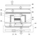
도 2는 본 발명의 일 실시 예에 따른 안테나 장치 및 이를 포함하는 전자 기기의 측단면도의 일부를 도시한 도면이고, 도 3은 본 발명의 일 실시 예에 따른 어레이 안테나가 형성된 전자 기기의 배면을 도시한 도면이다.FIG. 2 is a partial side cross-sectional view of an antenna device according to an embodiment of the present invention and an electronic device including the antenna device, and FIG. 3 is a rear view of an electronic device having an array antenna according to an embodiment of the present invention. It is an illustrated drawing.
도 2 및 도 3을 참고하면, 본 발명의 일 실시 예에 따른 전자 기기는, 어레이 안테나(210), RF(radio frequency) 모듈(220), 및 메인 기판(240)을 포함할 수 있다. 이때, 상기 전자 기기는 사용자 단말(UE: user equipment)일 수 있다. 예를 들면, 전자 기기는 휴대폰, 스마트폰(smart phone), PDA, 노트북 등 다른 네트워크 엔티티와 통신을 수행하는 전자 기기일 수 있다.Referring to FIGS. 2 and 3 , an electronic device according to an embodiment of the present invention may include an
상기 어레이 안테나(210)는 전자 기기의 금속 케이스(213)에 형성될 수 있으며, 적어도 2 개의 안테나 요소(antenna element)(215)를 포함할 수 있다. 그리고, 상기 적어도 2 개의 안테나 요소(215)들은 동일한 주파수 대역에서 동작할 수 있다. 또한, 실시 예에 따라서, 어레이 안테나(210)는 전자 기기의 금속 케이스(213)의 배면의 일부 영역에 형성될 수 있다. 도 2에서는 하나의 안테나 요소(215)만이 도시되어 있으나, 이는 설명의 편의를 위한 것으로, 전자기기의 금속 케이스(213)의 배면에 복수 개의 안테나 요소(215)들이 형성될 수 있다. 한편, 상기 금속 케이스(213)는 전도성 물질 및 열 전달 가능 물질로 구성될 수 있으며, 예를 들면, 상기 금속 케이스(213)는 알루미늄을 포함하는 금속으로 구성될 수 있다.The
또한, 각각의 안테나 요소(215)는 안테나의 신호를 전자기기의 외부로 방사하기 위한 방사부(211)를 포함할 수 있다. 그리고 상기 방사부(211)는 금속 케이스(213)의 배면에 형성되어, 안테나 요소(215)에서 방사된 신호가 전자기기의 외부로 방사되도록 할 수 있다. 이때, 상기 방사부(211)는 상기 금속 케이스(213)을 관통하는 슬롯(slot) 형태일 수 있으며, 원형, 사각형, 삼각형 등의 형태일 수 있다.In addition, each
도 3에 예시된 것과 같이, 전자 기기의 금속 케이스(213)의 배면에 어레이 안테나(210)가 형성될 수 있고, 상기 어레이 안테나(210)는 복수 개의 안테나 요소들(215)이 포함될 수 있다. 실시 예에 따라서, 상기 어레이 안테나(210)는 4행*4열의 16 개의 안테나 요소(215)들을 포함할 수 있다. 그리고, 안테나 요소(215)는 상기 금속 케이스(213)을 관통하는 슬롯(slot)(211)을 포함하는 패치(patch) 형태로 형성될 수 있다. 실시 예에 따라서, 각각의 안테나 요소(215)는 원형 또는 사각형 또는 사각형 형태일 수 있다. 그리고, 방사부(211)가 상기 원형 슬롯 형태인 경우, 방사부(211)는 2 개의 서로 마주보는 반원 형태의 슬롯으로 이루어질 수 있다. 이는, 안테나 요소(215)들이 금속 케이스(213)에서 분리되지 않고, 금속 케이스(213)에 일체형으로 결합된 일체형 어레이 안테나 구조를 갖도록 하기 위함이다. 한편, 안테나 요소(215)는 서로 마주보는 반원 형태의 2 개의 슬롯의 방사부(211)를 포함하고, 원형 또는 사각형 또는 삼각형 형태의 스택 커플 패치(stack couple patch) 형태로 이루어질 수 있고, 금속 케이스(213)와 일부 쇼팅(shorting)되어 있거나, 개방(open)되어 있을 수 있다.As illustrated in FIG. 3 , an
한편, 안테나가 금속 케이스(213)의 내부에 위치하는 경우에는 신호가 상기 금속 케이스(213)를 통과할 수 없으므로, 안테나가 신호를 방사하거나 또는 안테나가 신호를 수신하기 위해서는 금속 케이스(213)의 일부가 개방된 형태이어야 한다. 반면, 본원 발명에서와 같이, 어레이 안테나(210)가 전자 기기의 금속 케이스(213)의 배면에 일체형으로 형성된 경우, 금속 케이스(213)의 일부에 별도의 개구를 형성하지 않아도 상기 어레이 안테나(210)가 신호를 송수신할 수 있다.On the other hand, when the antenna is located inside the
그리고, 어레이 안테나(210)가 전자 기기의 금속 케이스(213)의 배면에 일체형으로 형성됨으로써, 어레이 안테나(210)에서 발생하는 열은 상기 금속 케이스(213)의 외부로 직접 방출될 수 있다.In addition, since the
또한, 금속 케이스(213)는 상기 금속 케이스(213)와 RF 모듈(230)을 결합하는 적어도 하나의 금속 케이스 연결 부재(217)를 포함할 수 있다. 상기 금속 케이스 연결 부재(217)는 나사(screw), 핀(pin) 등 다양한 형태의 연결 브릿지(bridge)일 수 있다.In addition, the
그리고, 상기 금속 케이스 연결 부재(217)는 열 전도가 가능한 열 전도 물질일 수 있다. 이때, 어레이 안테나(210)에서 발생한 열은 상기 금속 케이스 연결 부재(217)를 통해 RF 모듈(220)로 전달될 수 있다. 그리고, 상기 RF 모듈(220)로 전달된 열은, 후술할 열 방출 비아(via)(270) 및 열 방출부(미도시)를 통해 통해 전자 기기의 외부로 방출될 수 있다. 따라서, 상기 금속 케이스 연결 부재(217)는 열 방출 부재의 역할을 수행할 수 있으며, 따라서 상기 금속 케이스 연결 부재(217)는 어레이 안테나 열 방출 부재로 지칭될 수도 있다.Also, the metal
또한, 상기 금속 케이스(213)와 RF 모듈(220) 사이에는 빈 공간(cavity)가 형성되어 있을 수 있어, 어레이 안테나(210)에서 발생한 열이 상기 빈 공간을 통해 방출되어 발열 저감 효과가 있을 수 있다.In addition, since a cavity may be formed between the
이와 같이, 상기 어레이 안테나(210)가 전자 기기의 금속 케이스(213)에 일체형으로 형성됨으로써, 어레이 안테나(210)에서 발생한 열은 금속 케이스(213)를 통해 직접 전자 기기의 외부로 방출되거나, 금속 케이스 연결 부재(217)를 통해 전자 기기 내부의 열 방출부(미도시)를 통해 전자 기기의 외부로 방출될 수 있다. 즉, 본 발명의 일 실시 예에 따라서 어레이 안테나(210)가 전자 기기의 금속 케이스(213)에 일체형으로 형성되는 경우에, 어레이 안테나(210)에서 발생되는 열은 양 방향으로 확산됨으로써, 발열 저감 효과가 우수할 수 있다.As such, since the
실시 예에 따라서, 금속 케이스(213)는 내부에 내부 케이스(219)를 더 포함할 수 있고, 상기 배면 케이스(219)는 전자 기기의 내부 부속품들을 보호하기 위한 것으로 플라스틱, 금속 등으로 구성될 수 있다.Depending on the embodiment, the
RF 모듈(220)은 신호를 증폭 변환하는 동작을 하는 구성 요소로, 무선 주파수(radio frequency)를 송수신함으로써 다른 전자 기기와 무선 통신을 수행하도록 하는 동작을 할 수 있다. 이를 위해서 상기 동작을 수행하도록 제어하는 프로세서들(미도시)이 포함될 수 있다. 그리고, 외부 전원 공급부(미도시)는 RF 모듈(220)에게 전원을 공급할 수 있다. 또한, RF 모듈(220)은 RF 모듈 기판(221)을 포함할 수 있고, 상기 RF 모듈 기판(221)은 인쇄 회로 기판(PCB: printed circuit board)일 수 있다. 상기 RF 모듈 기판(221) 내에는 다수의 그라운드 층(227)이 형성되어 있을 수 있다. 그리고, 상기 RF 모듈 기판(221)의 상면에 형성된 상면 층(225)은 전자 기기의 금속 케이스(213)와 접촉할 수 있다. 그리고 상기 상면 층(225)은 절연 물질로 구성되어, RF 모듈(220)과 금속 케이스(213)을 절연하는 역할을 할 수 있다. 한편, 어레이 안테나(210)는 RF 모듈(220)의 RF 모듈 기판(221)에 표면 실장 기술(SMT: surface mounting technology), 나사(screw), 또는 포고 핀 블록(pogo pin block) 등을 이용하여 연결될 수 있다.The
그리고, 상기 RF 모듈(220)의 RF 모듈 기판(221) 내에는 복수 개의 열 방출 비아(270)가 형성되어 있을 수 있다. 상기 열 방출 비아(via)(270)는 RF 모듈(220) 및 RF 모듈(220)의 상부에 위치하는 어레이 안테나(210)에서 발생하는 열을 방출시키는 역할을 할 수 있다. 실시 예에 따라서, 상기 열 방출 비아(270)는 RF 모듈 기판(221)의 상면에서 하면 방향으로 형성된 비아(via)일 수 있다. 이에 따라, RF 모듈(220) 및 RF 모듈(220)의 상부에 위치하는 어레이 안테나(210)에서 발생한 열은 열 방출 비아(170)을 통해 RF 모듈(220)의 하부로 전달될 수 있다. 그리고, RF 모듈(220)의 하부로 전달된 열은, RF 모듈(220)의 하부에 위치하는 열 방출부(미도시)를 통해 방출될 수 있다. 한편, 상기 열 방출부(미도시)는 TIM(thermal interface material)일 수 있다. 이를 통해, 어레이 안테나(210) 및 RF 모듈(220)이 발열로 인해 발생할 수 있는 성능 저하(예를 들면, 이득 감소, 속도 저하 등)가 줄어들 수 있다.In addition, a plurality of
RF 모듈(220)의 RF 모듈 기판(221)의 하부에는 어레이 안테나(210)에 전력을 공급하는 RFIC(230)가 포함될 수 있다. 상기 RFIC(230)는 RF 모듈 기판(221) 내에 형성된 배선(250)을 통해 상기 어레이 안테나(210)에 전력을 공급할 수 있다.An
실시 예에 따라서, 상기 배선(250)과 어레이 안테나(210)의 연결은 도 2에 예시된 것과 같이 애퍼처 피딩(aperture feeding)으로 될 수 있다. 즉, RFIC(230)는 배선(250)에 전력을 공급하고, 상기 배선(250)에 공급된 전력은 어레이 안테나(210)에 포함되는 안테나 요소(215)와 커플링(coupling)을 통해 공급될 수 있다. 이를 위해서, 도면에 도시된 것과 같이 상기 상면 층(225)은 안테나 요소(215)에 대응하는 위치에 상면 개구부(226)를 포함할 수 있다. 상면 개구부(226)가 없는 경우, 배선(250)을 통해 공급된 신호는 RF 모듈 기판(221)의 상면 상에 형성된 절연성 상면 층(225)을 통과하지 못해, 안테나 요소(215)와 커플링이 이루어질 수 없다. 상면 층(225)의 상기 안테나 요소(215)에 대응하는 위치에 상면 개구부(226)가 형성된 경우에는 상기 상면 개구부(226)를 통해 배선(250)에 공급된 신호가 안테나 요소(215)로 전달될 수 있다.Depending on the embodiment, the connection between the
또는 실시 예에 따라서, RF 모듈 기판(221)의 상면 상에 상면 배선이 위치하고, 상기 상면 배선과 상기 배선(250)이 직접 연결(direct feeding)될 수 있다. 그리고, 상기 상면 배선과 어레이 안테나(210)의 안테나 요소(215)가 커플링이 되어 신호가 안테나 요소(215)로 공급될 수 있다. 이에 대한 구체적인 내용은 후술하도록 한다.Alternatively, according to the embodiment, a top surface wiring may be positioned on the top surface of the
한편, 메인 기판(240)은 전자 기기의 전반적인 동작을 제어할 수 있다. 이를 위해서 상기 동작을 수행하도록 제어하는 프로세서들(미도시)이 메인 기판(240)에 위치할 수 있다. 그리고, 외부 전원 공급부(미도시)는 메인 기판(240)에게 전원을 공급할 수 있다. 또한, 메인 기판(240)은 인쇄 회로 기판(221)일 수 있다.Meanwhile, the
그리고, 상기 메인 기판(240)과 RF 모듈(220)의 연결을 위한 메인 기판 연결 부재(260)가 상기 메인 기판(240)과 RF 모듈(220)의 사이에 위치할 수 있다. 실시 예에 따라서, 상기 메인 기판 연결 부재(260)와 RF 모듈(220) 사이에는 절연 부재(265)가 더 포함될 수 있다. 상기 메인 기판 연결 부재(260)는 볼 그리드 어레이(BGA: ball grid array)일 수 있으나, 이에 한정하는 것은 아니다. 예를 들면, 메인 기판 연결 부재(260)는 테이프, 필름, 전도성 테이프(conductive tape) 등일 수 있다. 또한, 실시 예에 따라 메인 기판(240)내에 RFIC(230)와 안테나(210)가 모두 일체화될 수도 있다.Also, a main
도 4는 본 발명의 일 실시 예에 따른 전자 기기의 열 방출 과정을 개략적으로 도시한 도면이다.4 is a diagram schematically illustrating a heat dissipation process of an electronic device according to an embodiment of the present invention.
도 4를 참고하면, 본 발명의 일 실시 예에 따른 전자 기기는 금속 케이스(213)의 배면에 일체형으로 형성된 어레이 안테나(210)를 포함할 수 있다. 이때, 상기 어레이 안테나(210)는 적어도 두 개의 안테나 요소(215)를 포함할 수 있고, 안테나 요소(215)들은 동일한 주파수 대역에서 동작할 수 있다. 그리고 상기 안테나 요소(215)는 안테나의 신호를 전자기기의 외부로 방사하기 위한 방사부(211)를 포함할 수 있다. 또한, 상기 금속 케이스(213)의 내부에는 내부 케이스(219)가 더 포함될 수 있다.Referring to FIG. 4 , an electronic device according to an embodiment of the present invention may include an
그리고, 상기 어레이 안테나(210)에는 RFIC(230)를 포함하는 RF 모듈(220)이 연결되고, 상기 RF 모듈(220)은 메인 기판(240)에 연결될 수 있다. 상기 메인 기판(240)의 상기 RF 모듈(220)이 연결된 면의 반대편 면에는 전자 기기의 제어부(410)가 포함될 수 있다. 상기 제어부(410)는 전자 기기를 제어하도록 하기 위한 적어도 하나의 프로세서(420)가 포함될 수 있고, 상기 프로세서(420)는 예를 들면 다이(die)일 수 있다. 그리고, 실시 예에 따라서 상기 제어부(410)에는 열 방출부(430)가 연결되어 전자 기기에서 발생하는 열을 방출할 수 있다. 상기 열 방출부(430)는 예를 들면, TIM일 수 있다.An
실시 예에 따라서, 제어부(410)가 메인 기판(240)과 연결되는 면의 반대편 면에는 지지부재(440)가 연결되어, 상기 제어부(410) 및 메인 기판(240)을 지지할 수 있다.Depending on the embodiment, a
또한, 전자 기기의 상면에는 방열 시트(450)와 표시부(460)가 형성될 수 있다. 상기 표시부(460)은 복수의 화소들이 행렬 형태로 배열된 패널일 수 있으며, 예를 들면, 액정 표시 장치(LDC: liquid crystal display), 유기 발광 다이오드(OLED: organic light emitting diode), 패시브 매트릭스형 유기 발광 표시 장치(PMOLED: passive matrix OLED), 액티브 매트릭스형 유기 발광 표시 장치(AMOLED: active matrix OLED) 등일 수 있다.In addition, a
이때, 도 4 및 도 3을 참고하면, 제어부(410)에서 발생한 열은 전도 방식으로 열 방출부(430), 메인 기판(240) 방향으로 전달될 수 있다. 열 방출부(430)로 전달된 열은 지지부재(440)를 통해 전도 또는 복사 형태로 방열 시트(450)로 전달되고, 이 열은 다시 전도 또는 복사 형태로 표시부(460)로 전달될 수 있다. 그리고, 표시부(460)에서는 대류 또는 복사 형태로 전자 기기의 외부로 열을 방출할 수 있다. 한편, 제어부(410)가 메인 기판(240)으로 전달한 열은 열 방출 비어(270)를 통해 RF 모듈(220)로 전도 또는 복사 형태로 전달될 수 있다. 그리고 RF 모듈(220)은 금속 케이스 연결 부재(217)를 통해 전도 또는 복사 형태로 열을 금속 케이스(213)로 전달하고, 이 열은 대류 또는 복사 형태로 전자 기기의 외부로 열을 방출할 수 있다.At this time, referring to FIGS. 4 and 3 , heat generated in the
어레이 안테나(210)에서 발생한 열은 금속 케이스(213)의 외부로 대류 또는 복사 형태로 바로 방출될 수 있다. 또한, 어레이 안테나(210)에서 발생한 열은 전도 또는 복사 형태로 RF 모듈(220)로 전달되고, 이는 다시 메인 기판(240)에 전달되고, 열 방출부(430)로 전도될 수 있다. 그리고 열 방출부(430)는 전도 또는 복사로 방열 시트(450)를 거쳐 표시부(460)를 통해 대류 또는 복사 형태로 전자 기기의 외부로 열을 방출할 수 있다.Heat generated from the
이와 같이 어레이 안테나(210)에서 발생한 열은 금속 케이스(213)를 통해 직접 전자 기기의 외부로 방출되거나, 금속 케이스 연결 부재(217)를 통해 전자 기기 내부의 열 방출부(430)를 통해 전자 기기의 외부로 방출될 수 있다.In this way, heat generated from the
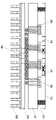
도 5는 본 발명의 일 실시 예에 따른 안테나 요소와 RF 모듈의 결합의 단면도를 도시한 도면이고, 도 6은 본 발명의 일 실시 예에 따른 안테나 요소 및 RF 모듈의 사시도의 일 예를 도시한 도면이고, 도 7은 본 발명의 일 실시 예에 따른 안테나 장치의 안테나 주파수 대역 성능을 보인 S11 그래프이고, 도 8은 본 발명의 일 실시 예에 따른 안테나 장치의 방사 패턴을 도시한 도면이다.5 is a cross-sectional view of a combination of an antenna element and an RF module according to an embodiment of the present invention, and FIG. 6 shows an example of a perspective view of an antenna element and an RF module according to an embodiment of the present invention. FIG. 7 is a graph S11 showing antenna frequency band performance of an antenna device according to an embodiment of the present invention, and FIG. 8 is a diagram showing a radiation pattern of an antenna device according to an embodiment of the present invention.
도 5 및 도 6의 (a)를 참고하면, 본 발명의 일 실시 예에 따른 전자 기기는 안테나 요소(215)들이 포함된 어레이 안테나(210)가 전자 기기의 금속 케이스(213)에 형성될 수 있다. 그리고, 안테나 요소(215)는 방사부(211)를 포함할 수 있고, 상기 방사부(211)는 상기 금속 케이스(213)을 관통하는 슬롯(slot)(211)형태일 수 있다. 실시 예에 따라서, 각각의 안테나 요소(215)는 원형 슬롯의 방사부(211)를 포함할 수 있으며, 상기 원형 슬롯은 2 개의 서로 마주보는 반원형태의 슬롯(211)으로 이루어질 수 있다.Referring to FIGS. 5 and 6(a) , in an electronic device according to an embodiment of the present invention, an
그리고, RF 모듈(210)이 상기 금속 케이스(213)에 결합할 수 있다. RF 모듈(210)은 상기 도 2 내지 도 4와 관련된 부분에서 설명한 것과 같이, RF 모듈 기판(221)의 내부에 어레이 안테나(210)에 전력을 공급하는 배선(250)이 포함될 수 있다. 그리고, RF 모듈(220)에서 발생한 열을 방출하기 위한 열 방출 비아(270)가 더 포함될 수 있다.Also, the
또한, RF 모듈 기판(221)의 상면 상에는 상면 층(225)이 형성되고, 상기 상면 층(225)은 안테나 요소(215)에 대응하는 위치에 상면 개구부(226)를 포함할 수 있다. 이때, 상기 상면 개구부(226)는 도 6의 (b)에 예시된 것과 같이 직선 형태로 되어 있을 수도 있고, 도 6의 (c)에 예시된 것과 같이 안테나 요소(215)와 동일한 원형 형태로 되어 있을 수도 있다.In addition, a
그리고, 상기 배선(250)은 도 5에 예시된 것과 같이 애퍼처 피딩(aperture feeding)으로 안테나 요소(215)에 연결될 수 있다. 좀 더 구체적으로 살펴보면, 배선(250)은 RF 모듈 기판(221)의 하면에서 연장되어 RF 모듈 기판(221)의 중간 층까지 연장될 수 있다. 예를 들면, RF 모듈 기판(221)이 4 개의 층으로 이루어진 경우에, 배선(250)은 제4 층에서 시작하여 제2 층의 상부까지 RF 모듈 기판(221)의 높이 방향으로 연장할 수 있다. 그리고 배선(250)은 제1 층과 제2 층 사이에서 RF 모듈 기판(221)의 면적 방향으로 적어도 상기 상면 개구부(226)까지 연장될 수 있다. 이 경우, 상면 층(225)의 상기 안테나 요소(215)에 대응하는 위치에 상면 개구부(226)가 형성되어 있으므로, 배선(250)에 공급된 신호는 어레이 안테나(210)에 포함되는 안테나 요소(215)와 커플링(coupling)을 통해 전달될 수 있다.Also, the
이와 같이, 본 발명의 일 실시 예에 따른 안테나 요소(215)와 RF 모듈(220)의 결합 구조는, IC, 기판(예를 들면, PCB), 금속 캐비티(metal cavity)의 결합 구조를 가질 수 있다. 그리고, 애퍼처 커플링 피딩(aperture coupling feeding) 방식을 통해 배선(250)과 안테나 요소(215)가 결합됨으로써, RF 모듈(210)이 최소 층을 이용해 임피던스(impedance)를 확보할 수 있다.As such, the coupling structure of the
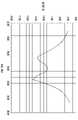
도 7을 참고하면, 금속 케이스(213)에 안테나 요소(215)가 결합된 안테나 구조에서 안테나 주파수 대역 성능을 보인 S11 그래프가 도시되어 있다. 그래프를 참고하면, S11이 나타내는 -10 dB 이하의 주파수는 약 26 내지 30 GHz로, 그 대역폭은 약 4 GHz 을 가질 수 있다. 이는 기존 패치 안테나의 대역폭 0.8 GHz에 비해서 약 3 GHz의 대역폭 개선 효과를 얻을 수 있음을 확인할 수 있다.Referring to FIG. 7 , a graph S11 showing antenna frequency band performance in an antenna structure in which an
그리고, 본 발명의 일 실시 예에 따른 안테나 장치의 방사 패턴을 도시한 도 8을 참고하면, 28 GHz의 주파수에서 주파수 이득은 약 6.03 dBi이고, 지향성(directivity)은 약 7.43 dBi일 수 있다. 그리고, 그에 따른 효율은 약 72.4 % 임을 확인할 수 있다. 이는 기존 패치 안테나의 이득이 4.46 dBi이고, 지향성이 6.99 dBi이며, 효율이 59.8%인 것에 비하여 그 효율 및 이득이 증가하는 것임을 알 수 있다.And, referring to FIG. 8 showing a radiation pattern of an antenna device according to an embodiment of the present invention, at a frequency of 28 GHz, the frequency gain may be about 6.03 dBi and the directivity may be about 7.43 dBi. And, it can be confirmed that the resulting efficiency is about 72.4%. It can be seen that the efficiency and gain are increased compared to the conventional patch antenna having a gain of 4.46 dBi, a directivity of 6.99 dBi, and an efficiency of 59.8%.
도 9는 본 발명의 일 실시 예에 따른 어레이 안테나의 일 예를 도시한 도면이고, 도 10은 본 발명의 일 실시 예에 따른 어레이 안테나의 안테나 주파수 대역 성능을 보인 S11 그래프이고, 도 11a 및 도 11b는 본 발명의 일 실시 예에 따른 어레이 안테나의 방사 패턴을 도시한 도면이다.9 is a diagram showing an example of an array antenna according to an embodiment of the present invention, and FIG. 10 is a graph S11 showing antenna frequency band performance of an array antenna according to an embodiment of the present invention, and FIGS. 11b is a diagram showing a radiation pattern of an array antenna according to an embodiment of the present invention.
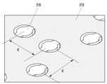
도 9를 참고하면, 본 발명의 일 실시 예에 따른 어레이 안테나(210)는 적어도 2 개의 안테나 요소(215)를 포함할 수 있다. 그리고, 상기 안테나 요소(215)는 전자 기기의 금속 케이스(213)에 형성될 수 있다.Referring to FIG. 9 , an
실시 예에 따라서, 어레이 안테나(210)는 도 9에 예시된 것과 같이 4행*4열의 16 개의 안테나 요소(215)들을 포함할 수 있다. 또한, 상기 도 2 내지 도 8과 관련된 부분에서 설명한 것과 같이 안테나 요소(215) 각각은 금속 케이스(213)를 관통하는 슬롯 형태의 방사부(211)를 포함할 수 있다. 이때, 상기 16 개의 안테나 요소(215)들 중 8 개는 전송용 안테나 요소이며, 나머지 8 개는 수신용 안테나 요소로 동작할 수도 있다.According to embodiments, the
상기 슬롯 형태의 방사부(211)는 2 개의 서로 마주보는 반원 형태의 슬롯으로 이루어질 수 있다. 이에 따라서, 안테나 요소(215)는 금속 케이스(213)에 일체형으로 결합될 수 있다.The slot-shaped
한편, 도시되지 않았지만, 상기 안테나 요소(215)는 원형 패치 형태가 아닌 다른 형태일 수도 있다. 예를 들면, 안테나 요소(215)는 타원형, 정사각형, 직사각형, 또는 삼각형 형태의 패치일 수도 있다. 그리고 상기 안테나 요소(215)의 방사부(211)도 타원형, 정사각형, 직사각형, 또는 삼각형 형태의 슬롯일 수도 있다.Meanwhile, although not shown, the
그리고, 상기 어레이 안테나(210)는 금속 가공 방식으로 설계될 수 있다. 예를 들면, CNC 가공 방식으로 어레이 안테나(210)의 안테나 요소(215)들을 금속 케이스(213)에 형성할 수 있다. 또는 3D 프린팅(printing) 방식으로 금속 케이스(213)를 가공하여 상기 어레이 안테나(210)를 형성할 수도 있다. 또는 실시 예에 따라서 2nd PCB (high end 또는 일반 FR4) 방식으로 금속 케이스(213)가 가공되어 어레이 안테나(210)가 제작될 수도 있을 것이다.Also, the
이와 같이 원형 슬롯(211)의 방사부를 포함하는 패치 형태의 안테나 요소(215)들이 포함된 어레이 안테나의 경우, 도 10을 참고하면, - 10 dB 이하의 주파수는 약 27.3 내지 29.5 GHz로, 그 대역폭은 약 2.2 GHz 을 가질 수 있다. 그리고, 도 11a 및 도 11b를 참고하면, 28 GHz에서의 방사 패턴이 도시되어 있는데, 이득은 약 17.85 dBi이고, 지향성은 18.3 dBi임을 확인할 수 있다. 그리고, 그에 따른 효율은 약 90% 임을 확인할 수 있다. 이는 기존 패치 안테나의 성능 대비, 이득은 약 2 dB, 대역폭은 약 1 GHz 개선되는 것을 확인할 수 있다.In the case of an array antenna including patch-shaped
도 12는 본 발명의 다른 일 실시 예에 따른 안테나 요소와 RF 모듈의 결합의 단면도를 도시한 도면이고, 도 13은 본 발명의 다른 일 실시 예에 따른 안테나 요소와 RF 모듈의 결합 상태의 사시도를 도시한 도면이고, 도 14는 본 발명의 다른 일 실시 예에 따른 안테나 요소와 RF 모듈이 결합된 경우 방사 효율을 도시한 도면이고, 도 15는 본 발명의 다른 일 실시 예에 따른 안테나 요소와 RF 모듈이 결합된 경우 안테나 주파수 대역 성능을 보인 S11 그래프이다.12 is a cross-sectional view of a combination of an antenna element and an RF module according to another embodiment of the present invention, and FIG. 13 is a perspective view of a coupled state of an antenna element and an RF module according to another embodiment of the present invention. 14 is a diagram showing radiation efficiency when an antenna element and an RF module are combined according to another embodiment of the present invention, and FIG. 15 is an antenna element and an RF module according to another embodiment of the present invention. It is a graph S11 showing the performance of the antenna frequency band when the modules are combined.
도 12의 (a)를 참고하면, 본 발명의 일 실시 예에 따른 전자 기기는, 전자 기기의 금속 케이스(213)에 안테나 요소(215)가 형성될 수 있다. 이때, 상기 안테나 요소(215)는 금속 케이스(213)를 관통하지 않는 슬롯 형태의 얇은 금속 막(1220)을 포함할 수 있다. 즉, 1220으로 도시된 것과 같이 안테나 요소(215)는 금속 케이스(213)에 얇은 금속 막을 넘겨둔 슬롯을 포함하는 패치 형태로 형성될 수 있다.Referring to (a) of FIG. 12 , in an electronic device according to an embodiment of the present invention, an
그리고, 상기 금속 케이스(213)의 상면을 애노다이징(anodizing) 기법으로 산화시킬 수 있다. 즉, 상기 애노디이징 기법을 적용하는 경우, 금속 케이스(213)의 상면이 산화, 부식되어 산화 막(1210)이 생성될 수 있다.In addition, the upper surface of the
애노디이징 기법을 적용하는 경우, 안테나 요소(215)를 형성하는 과정에서 금속 케이스(213)가 관통되지 않고 남은 얇은 금속 막(1220)은 산화되어 사라질 수 있다. 즉, 금속 케이스(213)를 관통하지 않는 슬롯 형태로 형성된 얇은 금속 막(1220)은, 금속 케이스(213)의 상면을 애노다이징 처리를 하는 과정에서 산화되어 사라지게 된다. 그러므로, 애노디이징 처리가 완료되면, 안테나 요소(215)는 금속 케이스(213)을 관통하는 슬롯 형태의 방사부(211)를 포함하게 될 수 있다. 이에 따라서, 금속 케이스(213)를 관통하는 원형의 슬롯(211)을 포함하는 안테나 요소(215)가 금속 케이스(213)에 일체형으로 형성될 수 있다.In the case of applying the anodizing technique, the
이와 같이, 금속 케이스(213)을 애노다이징 처리를 하는 것은, 외부의 영향으로부터 제품을 보호하는 역할을 할 수 있다. 또한, 금속 케이스(213)의 표면에 형성된 산화 막(1210)은 금속 케이스(213)를 관통하여 형성된 안테나 요소(215)들을 매끄럽게 처리하여 심미감도 높일 수 있다.In this way, anodizing the
그리고, 도 3, 도 6, 도 9에 예시적으로 도시된 것과 같이 안테나 요소(215)가 2 개의 서로 마주보는 반원형태의 슬롯(211)을 포함하지 않고, 도 13에 예시된 것과 같이 안테나 요소(215)는 개방된(open) 구조의 방사부를 포함할 수 있다. 즉, 금속 케이스(213)를 관통하는 하나의 원형 슬롯 형태의 방사부(1310)가 금속 케이스(213)에 일체형으로 결합되어 안테나 요소(215)에 포함될 수 있다. 좀 더 구체적으로 살펴보면, 안테나 요소(215)를 제작하는 과정에서 금속 케이스(213)의 상면을 관통하지 않는 원형의 슬롯을 포함하는 패치 형태로 안테나 요소(215)를 1차로 형성할 수 있다. 그리고, 2차로 금속 케이스(213)의 상면을 애노다이징 처리를 하여, 얇은 금속 막(1220)이 사라지게 할 수 있다. 그리고, 금속 케이스(213)를 관통하는 원형의 슬롯(1310)을 형성함으로써, 원형의 슬롯(1310) 방사부를 포함하는 안테나 요소(215)가 형성될 수 있다. 그리고, 상기 관통된 원형 슬롯(1310)으로 분리되는 원형 금속 판(1320)은 산화 막(1210)에 부착되어 떨어지지 않으므로, 안테나 요소(215)는 금속 케이스(213)에 일체형으로 형성될 수 있다.And, as exemplarily shown in FIGS. 3, 6, and 9, the
다음으로, 도 12의 (b)를 참고하면, 본 발명의 일 실시 예에 따른 전자 기기는, 전자 기기의 금속 케이스(213)에 안테나 요소(215)가 형성될 수 있다. 이때, 다이캐스팅(die casting) 및 사출 방법으로 안테나 요소(215)가 형성될 수 있다.Next, referring to (b) of FIG. 12 , in an electronic device according to an embodiment of the present invention, an
좀 더 구체적으로 살펴보면, 도 12의 (b)에 예시된 것과 같이 금속 케이스(213)을 관통하는 형태의 원형 슬롯(1240)으로 형성된 방사부를 포함하는 안테나 요소(215)가 다이캐스팅 방법으로 금속 케이스(213)에 형성될 수 있다. 그리고, 상기 금속 케이스(213)의 상면 상에 보완 재료 예를 들면, 폴리카보네이트(polycarbonate)를 포함하는 폴리카보네이트 막(1230)이 도포될 수 있다. 이렇게 함으로써, 상기 관통된 원형 슬롯(1240)으로 분리되는 원형 금속 판(1320)은 폴리카보네이트 막(1230)에 부착되어 떨어지지 않으므로, 안테나 요소(215)는 금속 케이스(213)에 일체형으로 형성될 수 있다. 따라서, 도 12의 (a) 및 도 13에 예시된 것과 같이 안테나 요소(215)는 개방된(open) 구조의 방사부(1240, 1310)를 포함할 수 있다.Looking more specifically, as illustrated in (b) of FIG. 12, the
이와 같이 개방된 구조의 방사부(1240, 1310)가 포함된 안테나 요소(215)를 포함하는 안테나 장치는 도 14에 예시된 것과 같이 그 효율이 90 %이며, 이득은 8.2 dBi일 수 있다. 그리고 도 15에 예시된 것과 같이 -10 dB 이하의 주파수는 약 22 GHz 이상의 대역으로 광대역(wideband) 특성을 가질 수 있다.The antenna device including the
도 16은 본 발명의 다른 일 실시 예에 따른 안테나 장치 및 이를 포함하는 전자 기기의 측단면도의 일부를 도시한 도면이고, 도 17은 본 발명의 일 실시 예에 따른 어레이 안테나 및 전력 증폭기의 결합 관계의 일 예를 도시한 도면이고, 도 18은 본 발명의 일 실시 예에 따른 어레이 안테나 및 전력 증폭기의 결합 관계의 다른 일 예를 도시한 도면이다.16 is a partial side cross-sectional view of an antenna device according to another embodiment of the present invention and an electronic device including the same, and FIG. 17 is a coupling relationship between an array antenna and a power amplifier according to an embodiment of the present invention. 18 is a diagram showing an example of a coupling relationship between an array antenna and a power amplifier according to an embodiment of the present invention.
도 16을 참고하면, 본 발명의 일 실시 예에 따른 전자 기기는, 어레이 안테나(210), RF 모듈(220), 및 메인 기판(240)을 포함할 수 있다. 이때, 상기 전자 기기는 기지국(base station, Node B, eNB(evolved Node B) 등)일 수 있다. 이하, 설명의 편의를 위해서 도 16에 도시된 각 구성 요소 중 도 2에 도시된 구성 요소와 동일한 구성 요소의 경우 그 구체적인 설명은 생략하기로 한다.Referring to FIG. 16 , an electronic device according to an embodiment of the present invention may include an
어레이 안테나(210)는 전자 기기의 금속 케이스(213)에 형성될 수 있으며, 적어도 2 개의 안테나 요소(215)를 포함할 수 있다. 그리고, 상기 적어도 2 개의 안테나 요소(215)들은 동일한 주파수 대역에서 동작할 수 있다. 그리고 상기 안테나 요소(215)는 안테나의 신호가 전자기기의 방사하기 위한 방사부(211)를 포함할 수 있다. 어레이 안테나(210)에 대해서는 상기 도 2 내지 도 15와 관련된 부분에서 설명하였으므로, 이에 대한 구체적인 설명은 생략하기로 한다.The
금속 케이스(213)는 금속 케이스(213)와 RF 모듈(220)을 결합하는 적어도 하나의 금속 케이스 연결 부재(217)를 포함할 수 있고, 열 전도가 가능한 열 전도 물질일 수 있다.The
그리고, RF 모듈(220)은 상기 어레이 안테나(210)와 상면 층(225)을 통해 연결될 수 있다. 그리고 RF 모듈(220)의 내부에는 열 방출 비아(270)이 RF 모듈의 RF 모듈 기판(221)의 상면에서 하면 방향으로 형성될 수 있다. 한편, 도 16에서는 배선(250)이 도시되어 있지 않으나, 이에 대해서는 도 17 및 도 18과 관련해서 후술하도록 한다.Also, the
RF 모듈 기판(221)의 하부에는 RFIC(230)이 위치하고, 상기 RFIC는 열 방출부(430)와 연결될 수 있다. 또한, RF 모듈(220)은 메인 기판(240)과 메인 기판 연결부재(260)를 통해 연결되고, 메인 기판(240)의 하부에는 상기 열 방출부(430)가 위치할 수 있다.An
한편, 도면에서는 RFIC(230)가 열 방출부(430)과 직접 연결되는 것으로 도시되어 있으나, 이에 한정하는 것은 아니다. 예를 들면, 도 2 및 도 3을 참고하면, RF 모듈(220)의 하부에는 메인 기판(240)이 위치하고, 상기 RFIC(230)의 상부에 메인 기판에 위치할 수 있다. 그리고, 상기 메인 기판(240)의 하부에 열 방출부(430)가 위치하고, RFIC(230)는 열 방출부(430)에 직접 연결되지 않을 수 있다.Meanwhile, in the drawing, the
한편, 도 16에 도시된 것과 같이, 전력 증폭기(PA)(290)는 RF 모듈(220)의 RF 모듈 기판(221)의 상면 상에 위치할 수 있다. 이때, 전력 증폭기(290)를 포함하는 프론트 엔드 모듈(FEM)이 상기 RF 모듈 기판(221)의 상면 상에 위치할 수도 있다. 다만, 설명의 편의를 위해서 전력 증폭기(290)가 RF 모듈 기판(221)의 상면 상에 위치하는 것을 예시적으로 설명하도록 한다.Meanwhile, as shown in FIG. 16 , the power amplifier (PA) 290 may be positioned on the upper surface of the
이때, 전력 증폭기(290)는 어레이 안테나(210)의 안테나 요소(215)들과 배선을 통해 연결될 수 있다. 그리고, 상기 전력 증폭기(290)는 RFIC(230)과 연결될 수 있다.In this case, the
이를 위해서, 도 17에 예시된 것과 같이 전력 증폭기(290)들과 어레이 안테나(210)는 동일 평면 상에 위치할 수 있다. 즉, 어레이 안테나(210)를 둘러싸고 전력 증폭기(290)들이 상기 어레이 안테나(210)와 동일 평면 상에 위치할 수 있다. 그리고, 안테나 요소(215)들 각각은 대응하는 전력 증폭기(290)에 배선을 통해 연결될 수 있다.To this end, as illustrated in FIG. 17 , the
또는 도 18 및 도 16에 예시된 것과 같이 전력 증폭기(290)들이 RF 모듈 기판(221)의 상면 상에 위치하고, 상기 전력 증폭기(290)의 상부에 어레이 안테나(210)가 위치할 수 있다. 즉, 전력 증폭기(290)와 어레이 안테나(210)가 적층된 구조를 가질 수도 있다. 이때, 도 18에 예시된 것과 같이 전력 증폭기(290)들 각각은 자신에 대응하는 안테나 요소(215)과 가장 근접하는 하부에 위치할 수 있다. 이 경우, 전력 증폭기(290)와 안테나 요소(215)의 배선 길이를 최소화할 수 있고, 안테나 장치의 크기도 줄일 수 있다.Alternatively, as illustrated in FIGS. 18 and 16 , the
도 19는 본 발명의 또 다른 일 실시 예에 따른 안테나 장치 및 이를 포함하는 전자 기기의 측단면도를 도시한 도면이고, 도 20은 본 발명의 또 다른 일 실시 예에 따른 안테나 장치 및 이를 포함하는 전자 기기의 사시도를 도시한 도면이고, 도 21은 본 발명의 또 다른 일 실시 예에 따른 안테나 장치 및 이를 포함하는 전자 기기의 분해도를 도시한 도면이고, 도 22는 본 발명의 일 실시 예에 따른 안테나 요소의 확대도를 도시한 도면이다.19 is a cross-sectional side view of an antenna device according to another embodiment of the present invention and an electronic device including the same, and FIG. 20 is an antenna device according to another embodiment of the present invention and an electronic device including the same. 21 is an exploded view of an antenna device and an electronic device including the antenna device according to another embodiment of the present invention, and FIG. 22 is an antenna according to an embodiment of the present invention. It is a drawing showing an enlarged view of an element.
도 19 내지 도 22를 참고하면, 열 방출부(430)의 상에 메인 기판(240)이 위치할 수 있다. 그리고, 상기 메인 기판(240)의 중심 영역에는 RFIC(230)이 실장될 수 있다. 이때, 상기 RFIC(230)가 메인 기판(240)과 동일 평면 상에 위치하기 위해서 메인 기판(240)의 중심 영역에 RFIC 수용 공간이 형성되어 있을 수 있다. 그리고, 상기 메인 기판(240)은 연결 부재(260)를 통해 RF 모듈 기판(221)과 연결될 수 있다.Referring to FIGS. 19 to 22 , the
상기 RF 모듈 기판(221)의 상부에는 복수 개의 전력 증폭기(290)이 위치할 수 있다. 그리고, 전력 증폭기(290)에서 발생되는 열을 열 방출부(280)로 방출하기 위해서, RF 모듈 기판(221)에서 열 방출 비아(270)가 형성될 수 있다. 이때, 열 방출 비아(270)는 전력 증폭기(290)가 위치하는 영역에 대응하여 RF 모듈 기판(221)의 높이 방향으로 형성될 수 있다.A plurality of
상기 복수 개의 전력 증폭기(290)의 상부에는 전도성 테이프(conductive tape) 등의 연결 부재(295)가 위치하여, 전력 증폭기(290)는 금속 케이스(213)에 연결될 수 있다.A connecting
그리고, 복수의 전력 증폭기(290)들 각각에 대응하는 안테나 요소들(215)은 자신에 대응하는 전력 증폭기(290)와 가장 가까운 영역에 형성되도록 금속 케이스(213)에 일체형으로 형성될 수 있다.In addition, the
또한 도 22를 참고하면, 각 안테나 요소(215)들 사이의 간격(d)은 약 0.5 내지 1 λ일 수 있다. 그리고, 안테나 요소(215)들은 쇼팅 핀(shorting pin) 형태로 금소 케이스(213)에 일체화될 수 있다.Also, referring to FIG. 22 , the interval d between each
상기 금속 케이스(213)에 일체형으로 안테나 요소들(215)이 형성됨으로써, 안테나 요소들(215)에서 발생한 열은 금속 케이스(213)를 통해 바로 전자 기기의 외부로 방출될 수 있다. 또한, 안테나 요소(215)에서의 신호 송수신도 금속 케이스(213)를 통해 바로 이루어짐으로써 방사 효율도 증가할 수 있다. 그리고, 외장 부품과의 인터리브드(interleaved) 배치를 통해 전송 인서션 로스(insertion loss)도 약 2 dB 개선될 수 있다.Since the
도 23은 본 발명의 일 실시 예에 따른 배선의 연결 방법에 대한 예들을 도시한 도면이다.23 is a diagram illustrating examples of a wiring connection method according to an embodiment of the present invention.
도 23의 첫 번째 및 두 번째 도면에서는 애퍼처 피딩(aperture feeding)의 일 예들이 도시되어 있다. 도 23의 첫 번째 도면를 참고하면, 배선(250)은 RF 모듈 기판(221)의 내부에 위치하고, RF 모듈 기판(221)의 상면 상에 위치하는 상면 배선(255)에 직접 연결되지 않을 수 있다. 그리고, 배선(250)과 상면 배선(255) 사이는 커플링에 의해 배선(250)에 공급된 신호가 상면 배선(255)에 전달될 수 있다. 그리고, 상기 상면 배선(255)과 안테나 요소(215) 사이의 또 다른 커플링으로 상기 상면 배선(255)에 공급된 신호가 안테나 요소(215)로 전달될 수 있다.In the first and second drawings of FIG. 23 , examples of aperture feeding are shown. Referring to the first drawing of FIG. 23 , the
도 23의 두 번째 도면 를 참고하면, 배선(250)은 RF 모듈 기판(221)의 내부에 위치하고, 상기 배선(250)은 안테나 요소(215)와 커플링을 통해 신호를 공급할 수 있다. 이때, 도면에서는 RF 모듈 기판(221)과 금속 케이스(213) 사이에 상면 층(225)이 도시되지 않았지만, RF 모듈 기판(221)과 금속 케이스(213) 사이에 상면 층(225)이 포함되는 경우, 도 2에 예시된 것과 같이, 상면 층(225)은 안테나 요소(215)에 대응하는 위치에 상면 개구부(226)를 포함할 수 있다.Referring to the second drawing of FIG. 23, the
다음으로, 도 23의 세 번째 및 네 번째 도면에서는 직접 연결(direct feeding)의 일 예들이 도시되어 있다. 도 23의 세 번째 및 네 번째 도면을 참고하면, 배선(250)은 RF 모듈 기판(221)의 내부에 위치하고, RF 모듈 기판(221)의 상면 상에 위치하는 상면 배선(255)에 직접 연결될 수 있다. 이에 따라, 상기 배선(250)에 공급된 신호는 상면 배선(255)에 직접 전달될 수 있다. 이후, 상면 배선(255)과 안테나 요소(215) 사이의 커플링으로 상기 상면 배선(255)에 공급된 신호가 안테나 요소(215)로 전달될 수 있다. 이때, 상면 배선(255)과 안테나 요소(215) 사이의 거리는 실시 예에 따라서 다를 수 있다. 따라서, 도 23의 세 번째 및 네 번째 도면에서와 같이 공급되는 신호의 세기, 구동 주파수 등에 따라서 상면 배선(255)과 안테나 요소(215) 사이의 거리는 달라질 수 있다.Next, examples of direct feeding are shown in the third and fourth drawings of FIG. 23 . Referring to the third and fourth views of FIG. 23 , the
도 24는 본 발명의 일 실시 예에 따른 안테나 요소, 전력 증폭기, RFIC의 연결 관계를 도시한 도면이고, 도 25 및 도 26은 본 발명의 일 실시 예에 따른 전력 증폭기의 전자 기기 내 배치 위치에 관하여 설명하는 도면이다.24 is a diagram showing a connection relationship between an antenna element, a power amplifier, and an RFIC according to an embodiment of the present invention, and FIGS. 25 and 26 are positions of a power amplifier according to an embodiment of the present invention in an electronic device. It is a drawing explaining about it.
도 24 및 도 25을 참고하면, 금속 케이스(213)에 일체형으로 안테나 요소(215)가 형성될 수 있다. 그리고, 상기 금속 케이스(213)의 하부에는 RF 모듈 기판(221)이 위치하고, 상기 RF 모듈 기판(221)의 하부에는 RFIC(230)이 위치할 수 있다.Referring to FIGS. 24 and 25 , the
이때, 전력 증폭기(290)는 RFIC(230)와 동일 평면 상에서 상기 RF 모듈 기판(221)의 하부에 위치할 수 있다. 그리고, RFIC(230)와 전력 증폭기(290)는 제2 배선(257)을 통해 연결되어, RFIC(230)에서 발생된 신호는 전력 증폭기(290)에서 증폭될 수 있다. 그리고, 전력 증폭기(290)와 상면 배선(255)은 제1 배선(250)을 통해 애퍼처 피딩에 따라 커플링 연결될 수 있다. 실시 예에 따라서 전력 증폭기(290)와 상면 배선(255)은 제1 배선(250)을 통해 직접 연결될 수도 있다.In this case, the
그리고, 상기 전력 증폭기(290)와 금속 케이스(213)를 연결하는 열 방출 비아(270)가 RF 모듈 기판(221)의 내부에 형성될 수 있다. 상기 열 방출 비아(270)를 통해, 전력 증폭기(290)에서 발생한 열은 금속 케이스(213)로 전달되고, 이 열은 금속 케이스(213)의 외부로 방출될 수 있다. 또한, 도시되지 않았지만, 전력 증폭기(290)의 하부에는 열 방출부(430)이 위치할 수 있어, 전력 증폭기(290)에서 발생한 열은 열 방출부(430)를 통해서도 전자 기기의 외부로 방출될 수 있다.In addition, a heat dissipation via 270 connecting the
다음으로 도 24 및 도 26을 참고하면, 도 25와 달리 전력 증폭기(290)는 RF 모듈 기판(221)의 상부에 위치할 수 있다. 그리고, 상기 전력 증폭기(290)가 위치하기 위해서 상기 금속 케이스(213)는 전력 증폭기 수용 공간이 형성되어 있을 수 있다.Next, referring to FIGS. 24 and 26 , unlike FIG. 25 , the
이때, RFIC(230)와 전력 증폭기(290)는 제2 배선(257)을 통해 연결되어, RFIC(230)에서 발생된 신호는 전력 증폭기(290)에서 증폭될 수 있다. 그리고, 전력 증폭기(290)와 상면 배선(255)은 제1 배선(250)을 통해 애퍼처 피딩에 따라 커플링 연결될 수 있다. 실시 예에 따라서 전력 증폭기(290)와 상면 배선(255)은 제1 배선(250)을 통해 직접 연결될 수도 있다.At this time, the
그리고, 상기 전력 증폭기(290)와 RF 모듈 기판(221)의 하부에 위치하는열방출부(430)를 연결하는 열 방출 비아(270)가 RF 모듈 기판(221)의 내부에 형성될 수 있다. 상기 열 방출 비아(270)를 통해, 전력 증폭기(290)에서 발생한 열은 열 방출부(430)에 전달되고, 상기 열 방출부(430)에 전달된 열은 전자 기기의 외부로 방출될 수 있다. 한편, 전력 증폭기(290)에서 발생한 열은 복사 또는 대류 방식으로, 전력 증폭기(290)의 상부에 위치하는 금속 케이스(213)에게 전달될 수도 있다. 그리고 상기 금속 케이스(213)에 전달된 열은 금속 케이스(213)의 외부로 방출될 수 있다.In addition, a heat dissipation via 270 connecting the
본 명세서와 도면에 개시된 실시 예는 기술 내용을 쉽게 설명하고, 이해를 돕기 위해 특정 예를 제시한 것일 뿐이며, 본 발명의 범위를 한정하고자 하는 것은 아니다. 여기에 개시된 실시 예들 이외에도 본 발명의 기술적 사상에 바탕을 둔 다른 변형 예들이 실시 가능하다는 것은 본 발명이 속하는 기술 분야에서 통상의 지식을 가진 자에게 자명한 것이다.Embodiments disclosed in this specification and drawings are only presented as specific examples to easily explain technical content and aid understanding, and are not intended to limit the scope of the present invention. It is obvious to those skilled in the art that other modified examples based on the technical spirit of the present invention can be implemented in addition to the embodiments disclosed herein.
한편, 본 명세서와 도면에는 본 발명의 바람직한 실시 예에 대하여 개시하였으며, 비록 특정 용어들이 사용되었으나, 이는 단지 본 발명의 기술 내용을 쉽게 설명하고 발명의 이해를 돕기 위한 일반적인 의미에서 사용된 것이지, 본 발명의 범위를 한정하고자 하는 것은 아니다. 여기에 개시된 실시 예 외에도 본 발명의 기술적 사상에 바탕을 둔 다른 변형 예들이 실시 가능하다는 것은 본 발명이 속하는 기술 분야에서 통상의 지식을 가진 자에게 자명한 것이다.On the other hand, preferred embodiments of the present invention have been disclosed in the present specification and drawings, and although specific terms have been used, they are only used in a general sense to easily explain the technical content of the present invention and help understanding of the present invention. It is not intended to limit the scope of the invention. It is obvious to those skilled in the art that other modified examples based on the technical idea of the present invention can be implemented in addition to the embodiments disclosed herein.
210: 어레이 안테나215: 안테나 요소
217: 금속 케이스 연결 부재220: RF 모듈
221: RF 모듈 기판230: RFIC
240: 메인 기판 250: 배선
260: 메인 기판 연결 부재270: 열 방출 비어
290: 전력 증폭기430: 열 방출부210: array antenna 215: antenna element
217: metal case connection member 220: RF module
221: RF module substrate 230: RFIC
240: main board 250: wiring
260: main board connection member 270: heat dissipation via
290: power amplifier 430: heat dissipation unit
Claims (20)
Translated fromKorean전자 기기의 금속 케이스에 형성된 어레이 안테나;
상기 금속 케이스의 하부에 위치하는 RF(radio frequency) 모듈;
상기 RF 모듈과 상기 금속 케이스를 연결하고, 상기 안테나 요소의 열을 방출하는 금속 케이스 연결 부재; 및
상기 RF 모듈의 내부에 형성되는 적어도 하나의 열 방출 비아(via)를 포함하고,
상기 어레이 안테나는 적어도 2 개의 안테나 요소(element)들을 포함하고,
상기 적어도 2 개의 안테나 요소들은 동일한 주파수 대역에서 동작하는 것을 특징으로 하는 안테나 장치.In the antenna device,
an array antenna formed in a metal case of an electronic device;
RF (radio frequency) module located under the metal case;
a metal case connecting member connecting the RF module and the metal case and dissipating heat from the antenna element; and
At least one heat dissipation via formed inside the RF module;
the array antenna includes at least two antenna elements;
The antenna device according to claim 1, wherein the at least two antenna elements operate in the same frequency band.
상기 적어도 2 개의 안테나 요소들 각각은 상기 금속 케이스를 관통하는 슬롯(slot) 형태의 방사부를 포함하고,
상기 상기 적어도 2 개의 안테나 요소들 각각은 원형, 사각형, 삼각형 중 어느 하나의 형태의 패치(patch) 안테나인 것을 특징으로 하는 안테나 장치.According to claim 1,
Each of the at least two antenna elements includes a slot-shaped radiation portion penetrating the metal case,
The antenna device, characterized in that each of the at least two antenna elements is a patch antenna having a shape of any one of a circular shape, a rectangular shape, and a triangle.
상기 방사부는 마주보는 반원 형태의 2개의 슬롯으로 이루어지는 것을 특징으로 하는 안테나 장치.According to claim 2,
The antenna device, characterized in that the radiation portion is composed of two slots in the form of a semicircle facing each other.
상기 방사부는 원형의 슬롯이고,
상기 금속 케이스의 상면에 형성된 산화 막 또는 폴리카보네이트 막을 더 포함하는 것을 특징으로 하는 안테나 장치.According to claim 2,
The radiation portion is a circular slot,
The antenna device further comprises an oxide film or a polycarbonate film formed on the upper surface of the metal case.
상기 RF 모듈의 상면에서, 상기 어레이 안테나를 둘러싸고 형성되는 적어도 하나의 전력 증폭기를 더 포함하는 것을 특징으로 하는 안테나 장치.According to claim 1,
and at least one power amplifier formed around the array antenna on the upper surface of the RF module.
상기 RF 모듈의 상면과 상기 어레이 안테나의 하면 사이에 위치하는 적어도 하나의 전력 증폭기를 더 포함하는 것을 특징으로 하는 안테나 장치.According to claim 1,
and at least one power amplifier positioned between the upper surface of the RF module and the lower surface of the array antenna.
상기 RF 모듈은 내부에 위치하는 배선을 더 포함하고,
상기 배선은 상기 어레이 안테나와 애퍼처 피딩(aperture feeding)으로 연결되고, 상기 안테나 요소에게 커플링을 통해 신호를 공급하는 것을 특징으로 하는 안테나 장치.According to claim 1,
The RF module further includes wiring located inside,
The wiring is connected to the array antenna through aperture feeding, and supplies a signal to the antenna element through coupling.
상기 RF 모듈의 상면에 위치하는 상면 배선; 및
상기 RF 모듈의 내부에 위치하고, 상기 상면 배선에 직접 연결되는 배선을 더 포함하는 것을 특징으로 하는 안테나 장치.According to claim 1,
an upper surface wiring located on an upper surface of the RF module; and
The antenna device further comprises a wire located inside the RF module and directly connected to the upper surface wire.
금속 케이스; 및
상기 금속 케이스에 형성된 어레이 안테나;
상기 금속 케이스의 하부에 위치하는 RF(radio frequency) 모듈;
상기 RF 모듈과 상기 금속 케이스를 연결하고, 상기 안테나 요소의 열을 방출하는 금속 케이스 연결 부재; 및
상기 RF 모듈의 내부에 형성되는 적어도 하나의 열 방출 비아(via)를 포함하고,
상기 어레이 안테나는 적어도 2 개의 안테나 요소(element)들을 포함하고,
상기 적어도 2 개의 안테나 요소들은 동일한 주파수 대역에서 동작하는 것을 특징으로 하는 전자 기기.In electronic devices,
metal case; and
an array antenna formed in the metal case;
RF (radio frequency) module located under the metal case;
a metal case connecting member connecting the RF module and the metal case and dissipating heat from the antenna element; and
At least one heat dissipation via formed inside the RF module;
the array antenna includes at least two antenna elements;
The electronic device according to claim 1, wherein the at least two antenna elements operate in the same frequency band.
상기 적어도 2 개의 안테나 요소들 각각은 상기 금속 케이스를 관통하는 슬롯(slot) 형태의 방사부를 포함하고,
상기 상기 적어도 2 개의 안테나 요소들 각각은 원형, 사각형, 삼각형 중 어느 하나의 형태의 패치(patch) 안테나인 것을 특징으로 하는 전자 기기.According to claim 11,
Each of the at least two antenna elements includes a slot-shaped radiation portion penetrating the metal case,
The electronic device, characterized in that each of the at least two antenna elements is a patch (patch) antenna of any one of circular, square, triangular shape.
상기 방사부는 서로 마주보는 반원 형태의 2개의 슬롯으로 이루어지는 것을 특징으로 하는 전자 기기.According to claim 12,
The electronic device, characterized in that the radiation portion is composed of two slots of a semicircular shape facing each other.
상기 방사부는 원형의 슬롯이고,
상기 금속 케이스의 상면에 형성된 산화 막 또는 폴리카보네이트 막을 더 포함하는 것을 특징으로 하는 전자 기기.According to claim 12,
The radiation portion is a circular slot,
An electronic device further comprising an oxide film or a polycarbonate film formed on an upper surface of the metal case.
상기 RF 모듈의 상면에서, 상기 어레이 안테나를 둘러싸고 형성되는 적어도 하나의 전력 증폭기를 더 포함하는 것을 특징으로 하는 전자 기기.According to claim 11,
The electronic device further comprises at least one power amplifier formed around the array antenna on the upper surface of the RF module.
상기 RF 모듈의 상면과 상기 어레이 안테나의 하면 사이에 위치하는 적어도 하나의 전력 증폭기를 더 포함하는 것을 특징으로 하는 전자 기기.According to claim 11,
The electronic device further comprises at least one power amplifier positioned between an upper surface of the RF module and a lower surface of the array antenna.
상기 RF 모듈은 내부에 위치하는 배선을 더 포함하고,
상기 배선은 상기 어레이 안테나와 애퍼처 피딩(aperture feeding)으로 연결되고, 상기 안테나 요소에게 커플링을 통해 신호를 공급하는 것을 특징으로 하는 전자 기기.According to claim 11,
The RF module further includes wiring located inside,
The wire is connected to the array antenna through aperture feeding, and supplies a signal to the antenna element through coupling.
상기 RF 모듈의 상면에 위치하는 상면 배선; 및
상기 RF 모듈의 내부에 위치하고, 상기 상면 배선에 직접 연결되는 배선을 더 포함하는 것을 특징으로 하는 전자 기기.According to claim 11,
an upper surface wiring located on an upper surface of the RF module; and
The electronic device further comprises a wiring located inside the RF module and directly connected to the top wiring.
Priority Applications (5)
| Application Number | Priority Date | Filing Date | Title |
|---|---|---|---|
| KR1020160111337AKR102501935B1 (en) | 2016-08-31 | 2016-08-31 | Antenna device and electronic device comprising the same |
| US16/319,963US11145949B2 (en) | 2016-08-31 | 2017-08-25 | Antenna apparatus and electronic device comprising same |
| EP17846924.3AEP3474380B1 (en) | 2016-08-31 | 2017-08-25 | Antenna apparatus and electronic device comprising same |
| CN201780052023.9ACN109643853B (en) | 2016-08-31 | 2017-08-25 | Antenna device and electronic equipment including the same |
| PCT/KR2017/009333WO2018043999A1 (en) | 2016-08-31 | 2017-08-25 | Antenna apparatus and electronic device comprising same |
Applications Claiming Priority (1)
| Application Number | Priority Date | Filing Date | Title |
|---|---|---|---|
| KR1020160111337AKR102501935B1 (en) | 2016-08-31 | 2016-08-31 | Antenna device and electronic device comprising the same |
Publications (2)
| Publication Number | Publication Date |
|---|---|
| KR20180024674A KR20180024674A (en) | 2018-03-08 |
| KR102501935B1true KR102501935B1 (en) | 2023-02-21 |
Family
ID=61300920
Family Applications (1)
| Application Number | Title | Priority Date | Filing Date |
|---|---|---|---|
| KR1020160111337AActiveKR102501935B1 (en) | 2016-08-31 | 2016-08-31 | Antenna device and electronic device comprising the same |
Country Status (5)
| Country | Link |
|---|---|
| US (1) | US11145949B2 (en) |
| EP (1) | EP3474380B1 (en) |
| KR (1) | KR102501935B1 (en) |
| CN (1) | CN109643853B (en) |
| WO (1) | WO2018043999A1 (en) |
Families Citing this family (18)
| Publication number | Priority date | Publication date | Assignee | Title |
|---|---|---|---|---|
| US11283190B2 (en)* | 2017-11-03 | 2022-03-22 | Avl Technologies, Inc. | Active fixed beam antenna array |
| KR102209123B1 (en) | 2017-12-19 | 2021-01-28 | 삼성전자 주식회사 | A module including an antenna and a radio frequency device and base station including the module |
| KR102068569B1 (en)* | 2018-04-05 | 2020-01-21 | 엘지전자 주식회사 | Mobile terminal |
| US10431872B1 (en) | 2018-04-05 | 2019-10-01 | Lg Electronics Inc. | Mobile terminal |
| US10306029B1 (en) | 2018-04-05 | 2019-05-28 | Lg Electronics Inc. | Mobile terminal |
| KR102068570B1 (en)* | 2018-04-05 | 2020-01-21 | 엘지전자 주식회사 | Mobile terminal |
| KR102069198B1 (en)* | 2018-04-09 | 2020-01-22 | 엘지전자 주식회사 | Mobile terminal |
| US10879585B2 (en) | 2018-04-09 | 2020-12-29 | Lg Electronics Inc. | Mobile terminal |
| KR102131417B1 (en)* | 2018-04-11 | 2020-07-08 | 주식회사 케이엠더블유 | Multi input and multi output antenna apparatus |
| KR102511096B1 (en) | 2018-04-11 | 2023-03-16 | 삼성전자 주식회사 | An electronic device including a cover combined with an antenna module |
| WO2019199078A1 (en)* | 2018-04-11 | 2019-10-17 | 주식회사 케이엠더블유 | Multiple input and multiple output antenna apparatus |
| US11056800B2 (en)* | 2018-10-16 | 2021-07-06 | Google Llc | Antenna arrays integrated into an electromagnetic transparent metallic surface |
| US20200280120A1 (en) | 2019-03-01 | 2020-09-03 | Microsoft Technology Licensing, Llc | High Frequency Antenna Integration in Electronic Devices |
| US11488796B2 (en)* | 2019-04-24 | 2022-11-01 | Applied Materials, Inc. | Thermal break for high-frequency antennae |
| KR102648537B1 (en) | 2019-09-19 | 2024-03-18 | 삼성전자주식회사 | An electronic device including an antenna module in which a heat transfer member is extended |
| KR102808980B1 (en)* | 2020-02-03 | 2025-05-21 | 삼성전자주식회사 | Electronic device including antenna module |
| US12132250B2 (en) | 2021-09-15 | 2024-10-29 | Samsung Electronics Co., Ltd. | Antenna module and electronic device including the same |
| US12347929B2 (en)* | 2022-08-12 | 2025-07-01 | Apple Inc. | Antenna feed structure |
Citations (2)
| Publication number | Priority date | Publication date | Assignee | Title |
|---|---|---|---|---|
| US20020122006A1 (en)* | 2001-03-05 | 2002-09-05 | Magis Networks, Inc. | Conformal box antenna |
| US20120262347A1 (en)* | 2009-12-23 | 2012-10-18 | Shoudong Tiang | Mobile terminal |
Family Cites Families (46)
| Publication number | Priority date | Publication date | Assignee | Title |
|---|---|---|---|---|
| US4032921A (en)* | 1975-09-08 | 1977-06-28 | American Electronic Laboratories, Inc. | Broad-band spiral-slot antenna |
| JPH03151702A (en) | 1989-11-08 | 1991-06-27 | Sony Corp | Plane array antenna |
| JP3356866B2 (en) | 1994-04-04 | 2002-12-16 | 日立化成工業株式会社 | Manufacturing method of triplate-fed planar antenna |
| KR100355263B1 (en)* | 1995-09-05 | 2002-12-31 | 가부시끼가이샤 히다치 세이사꾸쇼 | Coaxial Resonant Slot Antenna, Manufacturing Method and Portable Wireless Terminal |
| US6292140B1 (en)* | 1999-11-03 | 2001-09-18 | Hypres, Inc. | Antenna for millimeter-wave imaging and bolometer employing the antenna |
| US6326920B1 (en) | 2000-03-09 | 2001-12-04 | Avaya Technology Corp. | Sheet-metal antenna |
| US6329949B1 (en) | 2000-03-09 | 2001-12-11 | Avaya Technology Corp. | Transceiver stacked assembly |
| EP1445821A1 (en)* | 2003-02-06 | 2004-08-11 | Matsushita Electric Industrial Co., Ltd. | Portable radio communication apparatus provided with a boom portion |
| US7321337B2 (en) | 2003-05-15 | 2008-01-22 | Citizen Holdings Co., Ltd. | Electronic device having metal package unit having built-in antenna unit |
| KR100574014B1 (en)* | 2003-09-30 | 2006-04-26 | (주)에이스톤테크놀로지 | Broadband slot array antenna |
| US7411507B2 (en)* | 2004-08-20 | 2008-08-12 | Soundcraft, Inc. | Metal housing with integral antenna for RFID reader/writer |
| US7136017B2 (en)* | 2004-09-22 | 2006-11-14 | Navini Networks, Inc. | Pin fin ground plane for a patch antenna |
| US8800876B2 (en)* | 2008-08-11 | 2014-08-12 | Martin S. Casden | Ruggedized RFID tag and reader |
| EP2432641A4 (en)* | 2009-05-17 | 2012-10-10 | Hewlett Packard Development Co | Fluid-ejection printhead die having mixing barrier |
| US8659901B2 (en) | 2010-02-04 | 2014-02-25 | P-Wave-Holdings, LLC | Active antenna array heatsink |
| ES2632106T3 (en) | 2010-02-11 | 2017-09-08 | Soundcraft, Inc. | Reinforced Radio Frequency Identification Tag |
| US8610629B2 (en)* | 2010-05-27 | 2013-12-17 | Apple Inc. | Housing structures for optimizing location of emitted radio-frequency signals |
| US8847617B2 (en)* | 2011-04-22 | 2014-09-30 | Apple Inc. | Non-contact test system for determining whether electronic device structures contain manufacturing faults |
| US9107173B2 (en)* | 2011-07-28 | 2015-08-11 | Blackberry Limited | Method and system for access and uplink power control for a wireless system having multiple transmit points |
| US8648454B2 (en)* | 2012-02-14 | 2014-02-11 | International Business Machines Corporation | Wafer-scale package structures with integrated antennas |
| US9209523B2 (en)* | 2012-02-24 | 2015-12-08 | Futurewei Technologies, Inc. | Apparatus and method for modular multi-sector active antenna system |
| US9209513B2 (en)* | 2013-06-07 | 2015-12-08 | Apple Inc. | Antenna window and antenna pattern for electronic devices and methods of manufacturing the same |
| CN103700932B (en)* | 2013-12-27 | 2016-03-02 | 北京航天时代光电科技有限公司 | A kind of miniaturized very high frequency(VHF) monopole type antenna |
| US9728858B2 (en)* | 2014-04-24 | 2017-08-08 | Apple Inc. | Electronic devices with hybrid antennas |
| US9488719B2 (en) | 2014-05-30 | 2016-11-08 | Toyota Motor Engineering & Manufacturing North America, Inc. | Automotive radar sub-system packaging for robustness |
| US9391370B2 (en) | 2014-06-30 | 2016-07-12 | Samsung Electronics Co., Ltd. | Antenna feed integrated on multi-layer PCB |
| US9673511B2 (en) | 2014-09-22 | 2017-06-06 | Intel Corporation | Exciting dual frequency bands from an antenna component with a dual branch coupling feed |
| CN204231813U (en) | 2014-11-07 | 2015-03-25 | 联想(北京)有限公司 | Shell on the back and electronic equipment |
| US9871299B2 (en)* | 2014-12-04 | 2018-01-16 | Qualcomm Incorporated | Cavity backed aperture antenna |
| WO2016095836A1 (en) | 2014-12-18 | 2016-06-23 | 小米科技有限责任公司 | Electronic communication device with metal casing and manufacturing method therefor |
| CN106210181A (en) | 2014-12-18 | 2016-12-07 | 小米科技有限责任公司 | Electronics with metal shell and preparation method thereof |
| US10361476B2 (en) | 2015-05-26 | 2019-07-23 | Qualcomm Incorporated | Antenna structures for wireless communications |
| KR101606509B1 (en) | 2015-07-06 | 2016-03-25 | 엘아이지넥스원 주식회사 | Dual transit structure for millimeter-wave receiver |
| KR101559939B1 (en)* | 2015-07-07 | 2015-10-14 | 주식회사 아모그린텍 | Heat radiation unit for a wireless charging |
| US20170110787A1 (en)* | 2015-10-14 | 2017-04-20 | Apple Inc. | Electronic Devices With Millimeter Wave Antennas And Metal Housings |
| US10027180B1 (en)* | 2015-11-02 | 2018-07-17 | Energous Corporation | 3D triple linear antenna that acts as heat sink |
| US9743554B2 (en)* | 2015-11-18 | 2017-08-22 | Microsoft Technology Licensing, Llc | Heat dissipation in electronics with a heat spreader |
| US10547339B2 (en)* | 2016-01-29 | 2020-01-28 | Apple Inc. | Electronic devices having millimeter wave wireless data transfer capabilities |
| CN105633596B (en) | 2016-03-11 | 2019-08-16 | 中国电子科技集团公司第二十九研究所 | A kind of array antenna and its implementation of low thermal resistance connectorless feed |
| US9972892B2 (en)* | 2016-04-26 | 2018-05-15 | Apple Inc. | Electronic device with millimeter wave antennas on stacked printed circuits |
| US20170347490A1 (en)* | 2016-05-24 | 2017-11-30 | Texas Instruments Incorporated | High-frequency antenna structure with high thermal conductivity and high surface area |
| DE112016007571T5 (en)* | 2016-12-30 | 2019-10-24 | Intel Corporation | MICROELECTRONIC COMPONENTS DESIGNED WITH FLEXIBLE HOUSING SUBSTRATES WITH DISTRIBUTED STACKED ANTENNAS FOR HIGH FREQUENCY COMMUNICATION SYSTEMS |
| US10256549B2 (en)* | 2017-04-03 | 2019-04-09 | King Fahd University Of Petroleum And Minerals | Compact size, low profile, dual wideband, quasi-yagi, multiple-input multiple-output antenna system |
| US11075442B2 (en)* | 2017-05-31 | 2021-07-27 | Huawei Technologies Co., Ltd. | Broadband sub 6GHz massive MIMO antennas for electronic device |
| US10854953B2 (en)* | 2017-09-27 | 2020-12-01 | Apple Inc. | Electronic devices having housing-integrated antennas |
| US10431869B2 (en)* | 2017-12-19 | 2019-10-01 | Plume Design, Inc. | Slot antenna in compact wireless device |
- 2016
- 2016-08-31KRKR1020160111337Apatent/KR102501935B1/enactiveActive
- 2017
- 2017-08-25EPEP17846924.3Apatent/EP3474380B1/enactiveActive
- 2017-08-25WOPCT/KR2017/009333patent/WO2018043999A1/ennot_activeCeased
- 2017-08-25USUS16/319,963patent/US11145949B2/enactiveActive
- 2017-08-25CNCN201780052023.9Apatent/CN109643853B/enactiveActive
Patent Citations (2)
| Publication number | Priority date | Publication date | Assignee | Title |
|---|---|---|---|---|
| US20020122006A1 (en)* | 2001-03-05 | 2002-09-05 | Magis Networks, Inc. | Conformal box antenna |
| US20120262347A1 (en)* | 2009-12-23 | 2012-10-18 | Shoudong Tiang | Mobile terminal |
Also Published As
| Publication number | Publication date |
|---|---|
| CN109643853A (en) | 2019-04-16 |
| CN109643853B (en) | 2021-04-06 |
| EP3474380B1 (en) | 2021-05-05 |
| EP3474380A4 (en) | 2019-07-17 |
| US11145949B2 (en) | 2021-10-12 |
| US20190252757A1 (en) | 2019-08-15 |
| EP3474380A1 (en) | 2019-04-24 |
| KR20180024674A (en) | 2018-03-08 |
| WO2018043999A1 (en) | 2018-03-08 |
Similar Documents
| Publication | Publication Date | Title |
|---|---|---|
| KR102501935B1 (en) | Antenna device and electronic device comprising the same | |
| US11855353B2 (en) | Compact radio frequency (RF) communication modules with endfire and broadside antennas | |
| US10431892B2 (en) | Antenna-in-package structures with broadside and end-fire radiations | |
| JP7130164B2 (en) | Displays, display devices and electronic devices with integrated antennas | |
| US8836606B2 (en) | Coverage antenna apparatus with selectable horizontal and vertical polarization elements | |
| US10135149B2 (en) | Phased array for millimeter-wave mobile handsets and other devices | |
| KR100542829B1 (en) | High Gain Wideband Microstrip Patch Antenna for Transmit and Receive and Array Arrays | |
| US9716316B2 (en) | Substrate embedded horn antenna having selection capability of vertical and horizontal radiation pattern | |
| WO2016063759A1 (en) | Wireless communication module | |
| US20150194724A1 (en) | Millimeter wave antenna structures with air-gap layer or cavity | |
| US10770798B2 (en) | Flex cable fed antenna system | |
| TW200822455A (en) | Compact PCB antenna | |
| WO2020138448A1 (en) | Communication device | |
| US9972889B2 (en) | Multiband antenna and electronic apparatus having the same | |
| US12119539B2 (en) | Antenna module and communication device including the same | |
| KR102764145B1 (en) | Antenna device | |
| KR20190074569A (en) | Butler matrix anthena and manufacturing method thereof | |
| US12341235B2 (en) | Antenna module | |
| US20240047846A1 (en) | Antenna module | |
| TWI594507B (en) | Coaxial feed connection structure | |
| US20100123637A1 (en) | Antenna | |
| JP2006129227A (en) | Substrate mounted thin antenna | |
| CN117117495A (en) | Antenna device and terminal equipment |
Legal Events
| Date | Code | Title | Description |
|---|---|---|---|
| PA0109 | Patent application | Patent event code:PA01091R01D Comment text:Patent Application Patent event date:20160831 | |
| PG1501 | Laying open of application | ||
| A201 | Request for examination | ||
| PA0201 | Request for examination | Patent event code:PA02012R01D Patent event date:20210819 Comment text:Request for Examination of Application Patent event code:PA02011R01I Patent event date:20160831 Comment text:Patent Application | |
| PE0902 | Notice of grounds for rejection | Comment text:Notification of reason for refusal Patent event date:20220919 Patent event code:PE09021S01D | |
| E701 | Decision to grant or registration of patent right | ||
| PE0701 | Decision of registration | Patent event code:PE07011S01D Comment text:Decision to Grant Registration Patent event date:20230215 | |
| GRNT | Written decision to grant | ||
| PR0701 | Registration of establishment | Comment text:Registration of Establishment Patent event date:20230216 Patent event code:PR07011E01D | |
| PR1002 | Payment of registration fee | Payment date:20230217 End annual number:3 Start annual number:1 | |
| PG1601 | Publication of registration |