KR102500994B1 - Touch panel - Google Patents
Touch panelDownload PDFInfo
- Publication number
- KR102500994B1 KR102500994B1KR1020150141278AKR20150141278AKR102500994B1KR 102500994 B1KR102500994 B1KR 102500994B1KR 1020150141278 AKR1020150141278 AKR 1020150141278AKR 20150141278 AKR20150141278 AKR 20150141278AKR 102500994 B1KR102500994 B1KR 102500994B1
- Authority
- KR
- South Korea
- Prior art keywords
- display
- electrode
- substrate
- layer
- touch panel
- Prior art date
- Legal status (The legal status is an assumption and is not a legal conclusion. Google has not performed a legal analysis and makes no representation as to the accuracy of the status listed.)
- Active
Links
Images


Classifications
- G—PHYSICS
- G06—COMPUTING OR CALCULATING; COUNTING
- G06F—ELECTRIC DIGITAL DATA PROCESSING
- G06F3/00—Input arrangements for transferring data to be processed into a form capable of being handled by the computer; Output arrangements for transferring data from processing unit to output unit, e.g. interface arrangements
- G06F3/01—Input arrangements or combined input and output arrangements for interaction between user and computer
- G06F3/03—Arrangements for converting the position or the displacement of a member into a coded form
- G06F3/041—Digitisers, e.g. for touch screens or touch pads, characterised by the transducing means
- G06F3/0416—Control or interface arrangements specially adapted for digitisers
- G06F3/04166—Details of scanning methods, e.g. sampling time, grouping of sub areas or time sharing with display driving
- G—PHYSICS
- G06—COMPUTING OR CALCULATING; COUNTING
- G06F—ELECTRIC DIGITAL DATA PROCESSING
- G06F3/00—Input arrangements for transferring data to be processed into a form capable of being handled by the computer; Output arrangements for transferring data from processing unit to output unit, e.g. interface arrangements
- G06F3/01—Input arrangements or combined input and output arrangements for interaction between user and computer
- G06F3/03—Arrangements for converting the position or the displacement of a member into a coded form
- G06F3/041—Digitisers, e.g. for touch screens or touch pads, characterised by the transducing means
- G06F3/044—Digitisers, e.g. for touch screens or touch pads, characterised by the transducing means by capacitive means
- H—ELECTRICITY
- H10—SEMICONDUCTOR DEVICES; ELECTRIC SOLID-STATE DEVICES NOT OTHERWISE PROVIDED FOR
- H10K—ORGANIC ELECTRIC SOLID-STATE DEVICES
- H10K59/00—Integrated devices, or assemblies of multiple devices, comprising at least one organic light-emitting element covered by group H10K50/00
- H10K59/40—OLEDs integrated with touch screens
- H—ELECTRICITY
- H10—SEMICONDUCTOR DEVICES; ELECTRIC SOLID-STATE DEVICES NOT OTHERWISE PROVIDED FOR
- H10K—ORGANIC ELECTRIC SOLID-STATE DEVICES
- H10K50/00—Organic light-emitting devices
- H10K50/10—OLEDs or polymer light-emitting diodes [PLED]
- H10K50/11—OLEDs or polymer light-emitting diodes [PLED] characterised by the electroluminescent [EL] layers
- H10K50/125—OLEDs or polymer light-emitting diodes [PLED] characterised by the electroluminescent [EL] layers specially adapted for multicolour light emission, e.g. for emitting white light
- G—PHYSICS
- G06—COMPUTING OR CALCULATING; COUNTING
- G06F—ELECTRIC DIGITAL DATA PROCESSING
- G06F3/00—Input arrangements for transferring data to be processed into a form capable of being handled by the computer; Output arrangements for transferring data from processing unit to output unit, e.g. interface arrangements
- G06F3/01—Input arrangements or combined input and output arrangements for interaction between user and computer
- G06F3/03—Arrangements for converting the position or the displacement of a member into a coded form
- G06F3/041—Digitisers, e.g. for touch screens or touch pads, characterised by the transducing means
- G06F3/0412—Digitisers structurally integrated in a display
- G—PHYSICS
- G06—COMPUTING OR CALCULATING; COUNTING
- G06F—ELECTRIC DIGITAL DATA PROCESSING
- G06F3/00—Input arrangements for transferring data to be processed into a form capable of being handled by the computer; Output arrangements for transferring data from processing unit to output unit, e.g. interface arrangements
- G06F3/01—Input arrangements or combined input and output arrangements for interaction between user and computer
- G06F3/03—Arrangements for converting the position or the displacement of a member into a coded form
- G06F3/041—Digitisers, e.g. for touch screens or touch pads, characterised by the transducing means
- G06F3/0416—Control or interface arrangements specially adapted for digitisers
- G06F3/04164—Connections between sensors and controllers, e.g. routing lines between electrodes and connection pads
- G—PHYSICS
- G06—COMPUTING OR CALCULATING; COUNTING
- G06F—ELECTRIC DIGITAL DATA PROCESSING
- G06F3/00—Input arrangements for transferring data to be processed into a form capable of being handled by the computer; Output arrangements for transferring data from processing unit to output unit, e.g. interface arrangements
- G06F3/01—Input arrangements or combined input and output arrangements for interaction between user and computer
- G06F3/03—Arrangements for converting the position or the displacement of a member into a coded form
- G06F3/041—Digitisers, e.g. for touch screens or touch pads, characterised by the transducing means
- G06F3/044—Digitisers, e.g. for touch screens or touch pads, characterised by the transducing means by capacitive means
- G06F3/0443—Digitisers, e.g. for touch screens or touch pads, characterised by the transducing means by capacitive means using a single layer of sensing electrodes
- G—PHYSICS
- G06—COMPUTING OR CALCULATING; COUNTING
- G06F—ELECTRIC DIGITAL DATA PROCESSING
- G06F3/00—Input arrangements for transferring data to be processed into a form capable of being handled by the computer; Output arrangements for transferring data from processing unit to output unit, e.g. interface arrangements
- G06F3/01—Input arrangements or combined input and output arrangements for interaction between user and computer
- G06F3/03—Arrangements for converting the position or the displacement of a member into a coded form
- G06F3/041—Digitisers, e.g. for touch screens or touch pads, characterised by the transducing means
- G06F3/044—Digitisers, e.g. for touch screens or touch pads, characterised by the transducing means by capacitive means
- G06F3/0446—Digitisers, e.g. for touch screens or touch pads, characterised by the transducing means by capacitive means using a grid-like structure of electrodes in at least two directions, e.g. using row and column electrodes
- G—PHYSICS
- G06—COMPUTING OR CALCULATING; COUNTING
- G06F—ELECTRIC DIGITAL DATA PROCESSING
- G06F3/00—Input arrangements for transferring data to be processed into a form capable of being handled by the computer; Output arrangements for transferring data from processing unit to output unit, e.g. interface arrangements
- G06F3/01—Input arrangements or combined input and output arrangements for interaction between user and computer
- G06F3/03—Arrangements for converting the position or the displacement of a member into a coded form
- G06F3/041—Digitisers, e.g. for touch screens or touch pads, characterised by the transducing means
- G06F3/044—Digitisers, e.g. for touch screens or touch pads, characterised by the transducing means by capacitive means
- G06F3/0448—Details of the electrode shape, e.g. for enhancing the detection of touches, for generating specific electric field shapes, for enhancing display quality
- G—PHYSICS
- G09—EDUCATION; CRYPTOGRAPHY; DISPLAY; ADVERTISING; SEALS
- G09G—ARRANGEMENTS OR CIRCUITS FOR CONTROL OF INDICATING DEVICES USING STATIC MEANS TO PRESENT VARIABLE INFORMATION
- G09G3/00—Control arrangements or circuits, of interest only in connection with visual indicators other than cathode-ray tubes
- G09G3/20—Control arrangements or circuits, of interest only in connection with visual indicators other than cathode-ray tubes for presentation of an assembly of a number of characters, e.g. a page, by composing the assembly by combination of individual elements arranged in a matrix no fixed position being assigned to or needed to be assigned to the individual characters or partial characters
- G09G3/22—Control arrangements or circuits, of interest only in connection with visual indicators other than cathode-ray tubes for presentation of an assembly of a number of characters, e.g. a page, by composing the assembly by combination of individual elements arranged in a matrix no fixed position being assigned to or needed to be assigned to the individual characters or partial characters using controlled light sources
- G09G3/30—Control arrangements or circuits, of interest only in connection with visual indicators other than cathode-ray tubes for presentation of an assembly of a number of characters, e.g. a page, by composing the assembly by combination of individual elements arranged in a matrix no fixed position being assigned to or needed to be assigned to the individual characters or partial characters using controlled light sources using electroluminescent panels
- G09G3/32—Control arrangements or circuits, of interest only in connection with visual indicators other than cathode-ray tubes for presentation of an assembly of a number of characters, e.g. a page, by composing the assembly by combination of individual elements arranged in a matrix no fixed position being assigned to or needed to be assigned to the individual characters or partial characters using controlled light sources using electroluminescent panels semiconductive, e.g. using light-emitting diodes [LED]
- G09G3/3208—Control arrangements or circuits, of interest only in connection with visual indicators other than cathode-ray tubes for presentation of an assembly of a number of characters, e.g. a page, by composing the assembly by combination of individual elements arranged in a matrix no fixed position being assigned to or needed to be assigned to the individual characters or partial characters using controlled light sources using electroluminescent panels semiconductive, e.g. using light-emitting diodes [LED] organic, e.g. using organic light-emitting diodes [OLED]
- G09G3/3225—Control arrangements or circuits, of interest only in connection with visual indicators other than cathode-ray tubes for presentation of an assembly of a number of characters, e.g. a page, by composing the assembly by combination of individual elements arranged in a matrix no fixed position being assigned to or needed to be assigned to the individual characters or partial characters using controlled light sources using electroluminescent panels semiconductive, e.g. using light-emitting diodes [LED] organic, e.g. using organic light-emitting diodes [OLED] using an active matrix
- G09G3/3233—Control arrangements or circuits, of interest only in connection with visual indicators other than cathode-ray tubes for presentation of an assembly of a number of characters, e.g. a page, by composing the assembly by combination of individual elements arranged in a matrix no fixed position being assigned to or needed to be assigned to the individual characters or partial characters using controlled light sources using electroluminescent panels semiconductive, e.g. using light-emitting diodes [LED] organic, e.g. using organic light-emitting diodes [OLED] using an active matrix with pixel circuitry controlling the current through the light-emitting element
- H—ELECTRICITY
- H10—SEMICONDUCTOR DEVICES; ELECTRIC SOLID-STATE DEVICES NOT OTHERWISE PROVIDED FOR
- H10D—INORGANIC ELECTRIC SEMICONDUCTOR DEVICES
- H10D30/00—Field-effect transistors [FET]
- H10D30/60—Insulated-gate field-effect transistors [IGFET]
- H10D30/67—Thin-film transistors [TFT]
- H10D30/674—Thin-film transistors [TFT] characterised by the active materials
- H10D30/6755—Oxide semiconductors, e.g. zinc oxide, copper aluminium oxide or cadmium stannate
- H—ELECTRICITY
- H10—SEMICONDUCTOR DEVICES; ELECTRIC SOLID-STATE DEVICES NOT OTHERWISE PROVIDED FOR
- H10K—ORGANIC ELECTRIC SOLID-STATE DEVICES
- H10K59/00—Integrated devices, or assemblies of multiple devices, comprising at least one organic light-emitting element covered by group H10K50/00
- H10K59/10—OLED displays
- H10K59/12—Active-matrix OLED [AMOLED] displays
- H10K59/121—Active-matrix OLED [AMOLED] displays characterised by the geometry or disposition of pixel elements
- H10K59/1213—Active-matrix OLED [AMOLED] displays characterised by the geometry or disposition of pixel elements the pixel elements being TFTs
- H—ELECTRICITY
- H10—SEMICONDUCTOR DEVICES; ELECTRIC SOLID-STATE DEVICES NOT OTHERWISE PROVIDED FOR
- H10K—ORGANIC ELECTRIC SOLID-STATE DEVICES
- H10K59/00—Integrated devices, or assemblies of multiple devices, comprising at least one organic light-emitting element covered by group H10K50/00
- H10K59/10—OLED displays
- H10K59/12—Active-matrix OLED [AMOLED] displays
- H10K59/131—Interconnections, e.g. wiring lines or terminals
- H—ELECTRICITY
- H10—SEMICONDUCTOR DEVICES; ELECTRIC SOLID-STATE DEVICES NOT OTHERWISE PROVIDED FOR
- H10K—ORGANIC ELECTRIC SOLID-STATE DEVICES
- H10K59/00—Integrated devices, or assemblies of multiple devices, comprising at least one organic light-emitting element covered by group H10K50/00
- H10K59/30—Devices specially adapted for multicolour light emission
- H10K59/35—Devices specially adapted for multicolour light emission comprising red-green-blue [RGB] subpixels
- H—ELECTRICITY
- H10—SEMICONDUCTOR DEVICES; ELECTRIC SOLID-STATE DEVICES NOT OTHERWISE PROVIDED FOR
- H10K—ORGANIC ELECTRIC SOLID-STATE DEVICES
- H10K59/00—Integrated devices, or assemblies of multiple devices, comprising at least one organic light-emitting element covered by group H10K50/00
- H10K59/80—Constructional details
- H10K59/805—Electrodes
- H10K59/8051—Anodes
- H—ELECTRICITY
- H10—SEMICONDUCTOR DEVICES; ELECTRIC SOLID-STATE DEVICES NOT OTHERWISE PROVIDED FOR
- H10K—ORGANIC ELECTRIC SOLID-STATE DEVICES
- H10K59/00—Integrated devices, or assemblies of multiple devices, comprising at least one organic light-emitting element covered by group H10K50/00
- H10K59/80—Constructional details
- H10K59/805—Electrodes
- H10K59/8052—Cathodes
- G—PHYSICS
- G06—COMPUTING OR CALCULATING; COUNTING
- G06F—ELECTRIC DIGITAL DATA PROCESSING
- G06F2203/00—Indexing scheme relating to G06F3/00 - G06F3/048
- G06F2203/041—Indexing scheme relating to G06F3/041 - G06F3/045
- G06F2203/04112—Electrode mesh in capacitive digitiser: electrode for touch sensing is formed of a mesh of very fine, normally metallic, interconnected lines that are almost invisible to see. This provides a quite large but transparent electrode surface, without need for ITO or similar transparent conductive material
Landscapes
- Engineering & Computer Science (AREA)
- Theoretical Computer Science (AREA)
- General Engineering & Computer Science (AREA)
- Physics & Mathematics (AREA)
- General Physics & Mathematics (AREA)
- Human Computer Interaction (AREA)
- Computer Networks & Wireless Communication (AREA)
- Quality & Reliability (AREA)
- Microelectronics & Electronic Packaging (AREA)
- Computer Hardware Design (AREA)
- Geometry (AREA)
- Optics & Photonics (AREA)
- Devices For Indicating Variable Information By Combining Individual Elements (AREA)
- Electroluminescent Light Sources (AREA)
- Position Input By Displaying (AREA)
Abstract
Translated fromKoreanDescription
Translated fromKorean본 발명의 일 형태는 입력 장치에 관한 것이다. 본 발명의 일 형태는 표시 장치에 관한 것이다. 본 발명의 일 형태는 입출력 장치에 관한 것이다. 특히 본 발명의 일 형태는 터치 패널에 관한 것이다.One aspect of the present invention relates to an input device. One embodiment of the present invention relates to a display device. One aspect of the present invention relates to an input/output device. In particular, one aspect of the present invention relates to a touch panel.
또한 본 발명의 일 형태는 상술한 기술 분야에 한정되지 않는다. 본 발명의 일 형태가 속하는 기술 분야의 일례로서는 반도체 장치, 표시 장치, 발광 장치, 축전 장치, 기억 장치, 전자 기기, 조명 장치, 입력 장치, 입출력 장치, 이들의 구동 방법, 또는 이들의 제조 방법을 들 수 있다.In addition, one embodiment of the present invention is not limited to the technical field described above. As an example of the technical field to which one embodiment of the present invention belongs, a semiconductor device, a display device, a light emitting device, a power storage device, a memory device, an electronic device, a lighting device, an input device, an input/output device, a driving method thereof, or a manufacturing method thereof can be heard
또한 본 명세서에 있어서 반도체 장치란, 반도체 특성을 이용함으로써 기능할 수 있는 장치 전반을 가리킨다. 트랜지스터 등의 반도체 소자를 비롯하여 반도체 회로, 연산 장치, 기억 장치는 반도체의 일 형태이다. 촬상 장치, 표시 장치, 액정 표시 장치, 발광 장치, 입력 장치, 입출력 장치, 전기 광학 장치, 발전 장치(박막 태양 전지, 유기 박막 태양 전지 등을 포함함), 및 전자 기기는 반도체 장치를 갖는 경우가 있다.In this specification, a semiconductor device refers to all devices that can function by utilizing semiconductor characteristics. Semiconductor elements such as transistors, semiconductor circuits, arithmetic devices, and storage devices are one form of semiconductors. An imaging device, a display device, a liquid crystal display device, a light emitting device, an input device, an input/output device, an electro-optical device, a power generation device (including thin-film solar cells, organic thin-film solar cells, etc.), and electronic devices may include semiconductor devices. there is.
근년에 들어, 위치 입력 수단으로서 터치 센서를 탑재한 표시 장치가 실용화되고 있다. 터치 센서를 탑재한 표시 장치는 터치 패널, 또는 터치 스크린 등으로 불린다(이하, 단순히 터치 패널이라고도 부름). 예를 들어, 터치 패널을 구비하는 휴대 정보 단말로서는 스마트 폰, 태블릿 단말 등이 있다.In recent years, a display device equipped with a touch sensor as a position input means has been put into practical use. A display device equipped with a touch sensor is called a touch panel or a touch screen (hereinafter, simply referred to as a touch panel). For example, there exist a smart phone, a tablet terminal, etc. as a portable information terminal provided with a touch panel.
또한, 표시 장치로서는 대표적으로 액정 표시 장치, 유기 EL(Electro Luminescence) 소자나 발광 다이오드(LED:Light Emitting Diode) 등의 발광 소자를 구비하는 발광 장치, 전기 영동 방식 등에 의하여 표시를 하는 전자 페이퍼 등을 들 수 있다.In addition, as a display device, typically, a liquid crystal display device, a light emitting device including an organic EL (Electro Luminescence) element or a light emitting element such as a light emitting diode (LED: Light Emitting Diode), electronic paper displaying by an electrophoretic method, and the like can be heard
예를 들어, 유기 EL 소자의 기본적인 구성은 한 쌍의 전극 사이에 발광성의 유기 화합물을 포함하는 층을 끼운 것이다. 이 소자에 전압을 인가함으로써 발광성의 유기 화합물로부터 발광을 얻을 수 있다. 이러한 유기 EL 소자가 적용된 표시 장치는 액정 표시 장치 등에 필요한 백라이트가 불필요하므로 얇고, 가볍고, 콘트라스트가 높고, 소비 전력이 낮은 표시 장치를 구현할 수 있다. 예를 들어, 유기 EL 소자를 이용한 표시 장치의 일례가 특허문헌 1에 기재되어 있다.For example, the basic configuration of an organic EL device is to sandwich a layer containing a light emitting organic compound between a pair of electrodes. By applying a voltage to this element, light emission can be obtained from a light-emitting organic compound. A display device to which such an organic EL element is applied does not require a backlight required for a liquid crystal display device, and thus a display device that is thin, light, has high contrast, and consumes low power can be implemented. For example,
또한 터치 패널은 예를 들어 표시 패널 위에 중첩되도록 감압식의 센서 어레이, 또는 정전 용량식의 센서 어레이가 제공되고, 센서 어레이의 기판에 손끝이나 입력용 펜(스타일러스라고도 함)으로 접촉함으로써 접촉한 위치를 검지한다.In addition, the touch panel is provided with, for example, a pressure-sensitive sensor array or a capacitive sensor array so as to be superimposed on the display panel, and by contacting the substrate of the sensor array with a fingertip or an input pen (also called a stylus), the contacted position is detected. detect
특허문헌 2에는 일렉트로루미네센스 표시 장치의 표시 화면 위에 터치 센서를 제공한 터치 패널의 구성이 개시(開示)되어 있다.Patent Document 2 discloses a configuration of a touch panel provided with a touch sensor on a display screen of an electroluminescent display device.
터치 센서, 또는 터치 패널에 접촉되는 피검지체의 위치 정보를 더 정밀하게 취득하기 위하여 터치 센서의 고감도(高感度)화가 요구되고 있다.In order to more accurately acquire positional information of a touch sensor or a sensing object that is in contact with a touch panel, high sensitivity of the touch sensor is required.
본 발명의 일 형태는 검지 정밀도를 높일 수 있는 입력 장치, 또는 입출력 장치를 제공하는 것을 과제 중 하나로 한다. 또는 검출 감도를 높일 수 있는 입력 장치, 또는 입출력 장치를 제공하는 것을 과제 중 하나로 한다. 또는 신규 입력 장치, 또는 입출력 장치를 제공하는 것을 과제 중 하나로 한다.An object of one embodiment of the present invention is to provide an input device or an input/output device capable of increasing detection accuracy. Alternatively, one of the tasks is to provide an input device or an input/output device capable of increasing detection sensitivity. Alternatively, one of the tasks is to provide a new input device or input/output device.
또한 이들 과제의 기재는 다른 과제의 존재를 방해하는 것이 아니다. 또한 본 발명의 일 형태는 이들 과제 모두를 해결할 필요는 없는 것으로 한다. 또한 이들 외의 과제는 명세서, 도면, 청구항 등의 기재로부터 추출할 수 있다.In addition, the description of these subjects does not obstruct the existence of other subjects. In addition, one embodiment of the present invention assumes that it is not necessary to solve all of these problems. In addition, problems other than these can be extracted from descriptions such as specifications, drawings, and claims.
본 발명의 일 형태는 제 1 도전층과, 제 2 도전층과, 복수의 표시 소자와, 주사선을 갖는 터치 패널이다. 제 1 도전층은 평면에서 보았을 때 윤곽의 일부에, 제 1 방향에 평행한 직선 부분인 제 1 부분을 갖는다. 제 2 도전층은 평면에서 보았을 때 윤곽의 일부에 제 1 방향에 평행한 직선 부분인 제 2 부분을 갖는다. 제 1 부분과 제 2 부분은 대향하도록 제공된다. 표시 소자는 제 1 도전층 및 제 2 도전층과 중첩하지 않는 위치에 제공된다. 또한 주사선은 제 2 방향으로 연장되는 부분을 갖는다. 또한 제 1 방향과 제 2 방향이 이루는 각도가 30° 이상 60° 이하인 것이 특징이다.One aspect of the present invention is a touch panel including a first conductive layer, a second conductive layer, a plurality of display elements, and a scanning line. The first conductive layer has a first portion, which is a straight line portion parallel to the first direction, in a part of the contour in plan view. The second conductive layer has a second part, which is a straight line part parallel to the first direction, in a part of the contour in plan view. The first part and the second part are provided to face each other. The display element is provided at a position not overlapping the first conductive layer and the second conductive layer. Also, the scan line has a portion extending in the second direction. In addition, it is characterized in that the angle formed by the first direction and the second direction is 30° or more and 60° or less.
또한 상기에 있어서, 제 1 도전층 및 제 2 도전층은 제 1 방향 및 제 1 방향에 직교되는 방향으로 교차되는 격자 형상을 각각 갖고, 격자의 개구부와, 표시 소자가 서로 중첩되도록 배치되는 것이 바람직하다.Further, in the above, it is preferable that the first conductive layer and the second conductive layer each have a lattice shape that intersects in the first direction and in a direction orthogonal to the first direction, and the openings of the lattice and the display element are disposed so as to overlap each other. do.
또한 상기에 있어서, 표시 소자는 평면에서 보았을 때, 제 1 방향에 평행한 2변을 갖는 다각형 형상을 갖는 것이 바람직하다.Further, in the above, the display element preferably has a polygonal shape having two sides parallel to the first direction in plan view.
또한 상기에 있어서, 제 1 기판과, 제 2 기판을 갖고, 제 1 도전층, 제 2 도전층, 표시 소자, 및 주사선은, 제 1 기판과 제 2 기판 사이에 위치하는 것이 바람직하다. 또한 이때, 가시광을 차광하는 기능을 갖는 차광층을 갖고, 제 1 기판 위에 표시 소자 및 주사선이 제공되고, 제 2 기판 위에 제 1 도전층, 제 2 도전층, 및 차광층이 제공되어, 차광층은 제 1 도전층과 제 2 기판 사이, 및 제 2 도전층과 제 2 기판 사이에 위치하는 것이 바람직하다.Further, in the above, it is preferable to have a first substrate and a second substrate, and the first conductive layer, the second conductive layer, the display element, and the scanning line are positioned between the first substrate and the second substrate. Also at this time, a light blocking layer having a function of blocking visible light is provided, the display element and the scanning line are provided on the first substrate, and the first conductive layer, the second conductive layer, and the light blocking layer are provided on the second substrate. The silver is preferably located between the first conductive layer and the second substrate, and between the second conductive layer and the second substrate.
또한 상기에 있어서, 제 1 도전층과 제 2 도전층은 동일 평면 위에 형성되는 것이 바람직하다.Further, in the above, it is preferable that the first conductive layer and the second conductive layer are formed on the same plane.
또한 상기에 있어서, 제 1 부분과 제 2 부분의 거리가 1μm 이상 10mm 이하인 것이 바람직하다.Moreover, in the above, it is preferable that the distance between the 1st part and the 2nd part is 1 micrometer or more and 10 mm or less.
또한 본 발명의 다른 일 형태는 상기 터치 패널과, FPC를 갖는 터치 패널 모듈이다.Another aspect of the present invention is a touch panel module including the touch panel and an FPC.
또한 본 발명의 다른 일 형태는 상기 터치 패널, 또는 터치 패널 모듈과, 안테나, 버튼, 전지, 스피커, 마이크로폰, 또는 렌즈 중 적어도 하나를 갖는 전자 기기이다.Another aspect of the present invention is an electronic device having at least one of the touch panel or touch panel module, an antenna, a button, a battery, a speaker, a microphone, or a lens.
본 발명의 일 형태에 따르면, 검지 정밀도를 높일 수 있는 입력 장치, 또는 입출력 장치를 제공할 수 있다. 또는 검출 감도를 높일 수 있는 입력 장치, 또는 입출력 장치를 제공할 수 있다. 또는 신규 입력 장치, 또는 입출력 장치를 제공할 수 있다.According to one embodiment of the present invention, an input device or input/output device capable of increasing detection accuracy can be provided. Alternatively, an input device or an input/output device capable of increasing detection sensitivity may be provided. Alternatively, a new input device or input/output device may be provided.
또한 이들 효과의 기재는 다른 효과의 존재를 방해하는 것이 아니다. 또한 본 발명의 일 형태는 반드시 이들 효과 모두를 가질 필요는 없다. 또한 이들 외의 효과는 명세서, 도면, 청구항 등의 기재로부터 추출할 수 있다.Also, the description of these effects does not preclude the existence of other effects. In addition, one embodiment of the present invention does not necessarily have all of these effects. In addition, effects other than these can be extracted from descriptions such as specifications, drawings, and claims.
도 1은 실시형태에 따른 터치 패널의 구성예.
도 2는 실시형태에 따른 입력 장치의 구성예.
도 3은 실시형태에 따른 입력 장치의 구성예.
도 4는 실시형태에 따른 입력 장치의 구성예.
도 5는 실시형태에 따른 입력 장치의 구성예.
도 6은 실시형태에 따른 입력 장치의 구성예.
도 7은 실시형태에 따른 입력 장치의 구성예.
도 8은 실시형태에 따른 입력 장치의 구성예.
도 9는 실시형태에 따른 입력 장치의 구성예.
도 10은 실시형태에 따른 터치 패널의 구성예.
도 11은 실시형태에 따른 터치 패널의 구성예.
도 12는 실시형태에 따른 터치 패널의 구성예.
도 13은 실시형태에 따른 터치 패널의 구성예.
도 14는 실시형태에 따른 터치 패널의 구성예.
도 15는 실시형태에 따른 터치 패널의 구성예.
도 16은 실시형태에 따른 터치 패널의 구성예.
도 17은 실시형태에 따른 터치 패널의 구성예.
도 18은 실시형태에 따른 터치 패널의 구성예.
도 19는 실시형태에 따른 터치 패널의 구성예.
도 20은 실시형태에 따른 터치 패널의 구성예.
도 21은 실시형태에 따른 터치 패널의 구성예.
도 22는 실시형태에 따른 터치 패널의 구성예.
도 23은 실시형태에 따른 터치 패널의 구성예.
도 24는 실시형태에 따른 터치 패널의 구성예.
도 25는 실시형태에 따른 터치 패널의 구성예.
도 26은 실시형태에 따른 터치 패널의 구성예.
도 27은 실시형태에 따른 터치 패널의 구성예.
도 28은 실시형태에 따른 터치 센서의 블록도 및 타이밍 차트도.
도 29는 실시형태에 따른 터치 센서의 회로도.
도 30은 실시형태에 따른 터치 센서를 구비하는 화소를 설명하는 도면.
도 31은 실시형태에 따른 터치 센서 및 화소의 동작을 설명하는 도면.
도 32는 실시형태에 따른 전자 기기 및 조명 장치의 일례를 도시한 도면.
도 33은 실시형태에 따른 전자 기기의 일례를 도시한 도면.
도 34는 실시형태에 따른 전자 기기의 일례를 도시한 도면.
도 35는 실시형태에 따른 전자 기기의 일례를 도시한 도면.1 is a configuration example of a touch panel according to an embodiment.
2 is a configuration example of an input device according to an embodiment.
3 is a configuration example of an input device according to an embodiment.
4 is a configuration example of an input device according to an embodiment.
5 is a configuration example of an input device according to an embodiment.
6 is a configuration example of an input device according to an embodiment.
7 is a configuration example of an input device according to an embodiment.
8 is a configuration example of an input device according to an embodiment.
9 is a configuration example of an input device according to an embodiment.
10 is a configuration example of a touch panel according to an embodiment.
11 is a configuration example of a touch panel according to an embodiment.
12 is a configuration example of a touch panel according to an embodiment.
13 is a configuration example of a touch panel according to an embodiment.
14 is a configuration example of a touch panel according to an embodiment.
15 is a configuration example of a touch panel according to an embodiment.
16 is a configuration example of a touch panel according to an embodiment.
17 is a configuration example of a touch panel according to an embodiment.
18 is a configuration example of a touch panel according to an embodiment.
19 is a configuration example of a touch panel according to an embodiment.
20 is a configuration example of a touch panel according to an embodiment.
21 is a configuration example of a touch panel according to an embodiment.
22 is a configuration example of a touch panel according to an embodiment.
23 is a configuration example of a touch panel according to an embodiment.
24 is a configuration example of a touch panel according to an embodiment.
25 is a configuration example of a touch panel according to an embodiment.
26 is a configuration example of a touch panel according to an embodiment.
27 is a configuration example of a touch panel according to an embodiment;
28 is a block diagram and timing chart diagram of a touch sensor according to an embodiment;
29 is a circuit diagram of a touch sensor according to an embodiment.
30 is a diagram for explaining a pixel having a touch sensor according to an embodiment;
31 is a diagram explaining operations of a touch sensor and pixels according to an embodiment;
32 is a diagram showing an example of an electronic device and a lighting device according to an embodiment;
33 is a diagram showing an example of an electronic device according to an embodiment;
34 is a diagram showing an example of an electronic device according to an embodiment;
35 is a diagram showing an example of an electronic device according to an embodiment;
실시형태에 대하여 도면을 참조하여 자세히 설명한다. 다만, 본 발명은 이하의 설명에 한정되지 않고, 본 발명의 취지 및 그 범위에서 벗어남이 없이 그 형태 및 자세한 내용을 다양하게 변경할 수 있는 것은 당업자라면 쉽게 이해할 수 있다. 따라서, 본 발명은 이하에서 제시하는 실시형태의 기재 내용에 한정되어 해석되는 것이 아니다.An embodiment will be described in detail with reference to the drawings. However, the present invention is not limited to the following description, and it is easily understood by those skilled in the art that the form and details can be variously changed without departing from the spirit and scope of the present invention. Therefore, the present invention is not construed as being limited to the description of the embodiments presented below.
또한 이하에서 설명하는 발명의 구성에 있어서, 동일한 부분 또는 같은 기능을 갖는 부분에는 동일한 부호를 상이한 도면간에서 공통적으로 사용하여 반복되는 설명을 생략한다. 또한 같은 기능을 갖는 부분을 가리키는 경우에는 해치 패턴을 동일한 것으로 하여 특별히 부호를 부여하지 않는다.In the configuration of the invention described below, the same reference numerals are commonly used in different drawings for the same parts or parts having the same functions, and repeated explanations are omitted. In addition, when pointing to parts having the same function, hatch patterns are assumed to be the same and no special code is given.
또한 본 명세서에서 설명되는 각 도면에 있어서, 각 구성의 크기, 층 두께, 또는 영역은 명료화를 위하여 과장된 경우가 있다. 따라서, 반드시 그 스케일에 한정되는 것은 아니다.In addition, in each drawing described in this specification, the size, layer thickness, or area of each component may be exaggerated for clarity. Therefore, it is not necessarily limited to that scale.
또한 본 명세서에서의 '제 1', '제 2' 등의 서수사는 구성 요소의 혼동을 피하기 위하여 부여하는 것이고 수적으로 한정하는 것이 아니다.In addition, ordinal numbers such as 'first' and 'second' in this specification are given to avoid confusion among components and are not limited numerically.
트랜지스터는 반도체 소자의 종류 중 하나이고, 전류나 전압의 증폭이나, 도통 또는 비도통을 제어하는 스위칭 동작 등을 실현할 수 있다. 본 명세서에서의 트랜지스터는 IGFET(Insulated Gate Field Effect Transistor)나 박막 트랜지스터(TFT:Thin Film Transistor)를 포함한다.A transistor is one of the types of semiconductor devices, and can realize current or voltage amplification or a switching operation for controlling conduction or non-conduction. The transistor in this specification includes an Insulated Gate Field Effect Transistor (IGFET) or a Thin Film Transistor (TFT).
(실시형태 1)(Embodiment 1)
본 실시형태에서는 본 발명의 일 형태의 입력 장치(터치 센서)의 구성예, 및 본 발명의 일 형태의 입력 장치와 표시 장치(표시 패널)를 구비하는 입출력 장치(터치 패널)의 구성예에 대하여 도면을 참조하여 설명한다.In the present embodiment, a configuration example of an input device (touch sensor) of one embodiment of the present invention and a configuration example of an input/output device (touch panel) including an input device and a display device (display panel) of one embodiment of the present invention It demonstrates with reference to drawings.
이하에서는 본 발명의 일 형태의 터치 센서로서 정전 용량 방식의 터치 센서를 적용한 경우에 대하여 설명한다.Hereinafter, a case in which a capacitive touch sensor is applied as a touch sensor according to one embodiment of the present invention will be described.
또한 본 명세서 등에서, 터치 패널은 표시면에 화상을 표시(출력)하는 기능과 표시면에 손가락이나 스타일러스 등의 피검지체가 접촉되거나 근접하는 것을 검출하는 터치 센서로서의 기능을 갖는다. 따라서, 터치 패널은 입출력 장치의 일 형태이다.Also, in this specification and the like, the touch panel has a function of displaying (outputting) an image on the display surface and a function of a touch sensor that detects contact or proximity of a sensing target such as a finger or a stylus to the display surface. Accordingly, the touch panel is a type of input/output device.
또한 본 명세서에서는 터치 패널의 기판에 예를 들어 FPC(Flexible Printed Circuit) 또는 TCP(Tape Carrier Package) 등의 커넥터가 제공된 것, 또는 기판에 COG(Chip On Glass) 방식에 의하여 IC(집적 회로)가 실장된 것을 터치 패널 모듈, 또는 단순히 터치 패널이라고 부르는 경우가 있다.In addition, in the present specification, a connector such as FPC (Flexible Printed Circuit) or TCP (Tape Carrier Package) is provided on the substrate of the touch panel, or an IC (Integrated Circuit) is provided on the substrate by the COG (Chip On Glass) method. There are cases where a mounted one is called a touch panel module or simply a touch panel.
본 발명의 일 형태에 적용할 수 있는 정전 용량 방식의 터치 센서는 한 쌍의 도전층을 구비한다. 한 쌍의 도전층 사이에는 용량이 형성된다. 한 쌍의 도전층에 피검지체가 접촉되거나 근접함으로써 한 쌍의 도전층 사이의 용량의 크기가 변화하는 것을 이용하여 검출을 할 수 있다.A capacitive touch sensor applicable to one embodiment of the present invention includes a pair of conductive layers. Capacitance is formed between the pair of conductive layers. Detection can be performed using a change in capacitance between the pair of conductive layers when a sensing target is brought into contact with or approached to the pair of conductive layers.
정전 용량 방식으로서는 표면형 정전 용량 방식, 투영형 정전 용량 방식 등이 있다. 투영형 정전 용량 방식으로서는 자기 용량 방식, 상호 용량 방식 등이 있다. 상호 용량 방식을 이용하면 동시 다점 검출이 가능하기 때문에 바람직하다.Capacitance methods include a surface type capacitance method, a projected capacitance method, and the like. As the projected capacitance method, there are a self-capacitance method, a mutual capacitance method, and the like. The mutual capacitance method is preferable because simultaneous multi-point detection is possible.
한 쌍의 도전층은 평면에서 보았을 때의 윤곽의 일부에 직선 부분을 갖는다. 또한 2개의 도전층은 각각의 직선 부분이 평행이 되도록 대향하여 배치된다. 이러한 구성으로 함으로써 2개의 도전층 사이에 형성되는 용량의 크기를 크게 할 수 있다. 또한 2개의 도전층이 평행하게 대향하는 부분에 있어서, 2개의 도전층 사이에 전위차를 주었을 때에 생기는 전기력선은 밀도가 균일하게 분포되므로 장소에 따라 검출 감도의 차이가 생기는 것을 억제할 수 있다. 그러므로 검지 정밀도가 높은 터치 센서를 실현할 수 있다.The pair of conductive layers have a straight line part in a part of the contour in plan view. Also, the two conductive layers are disposed oppositely so that each straight line portion is parallel. With this configuration, the size of the capacitance formed between the two conductive layers can be increased. In addition, in a portion where two conductive layers face each other in parallel, the density of electric force lines generated when a potential difference is applied between the two conductive layers is uniformly distributed, so that the difference in detection sensitivity depending on the location can be suppressed. Therefore, a touch sensor with high detection accuracy can be realized.
본 발명의 일 형태의 터치 패널은 터치 센서와, 화상을 표시하는 표시 패널(표시 장치)을 갖는다. 터치 센서는 표시 패널의 표시면 측에 중첩되어 제공된다.A touch panel of one embodiment of the present invention includes a touch sensor and a display panel (display device) that displays an image. The touch sensor is provided overlapping the display surface side of the display panel.
또한 표시 패널이 갖는 표시 소자와 터치 센서를 구성하는 한 쌍의 도전층이 중첩하지 않도록 제공하는 것이 바람직하다. 이로써 터치 패널이 표시하는 화상의 휘도가 저하되는 것을 방지하여 시인성이 높은 터치 패널을 실현할 수 있다. 더구나 소비 전력을 저감할 수 있다.In addition, it is preferable to provide a display element included in the display panel and a pair of conductive layers constituting the touch sensor so that they do not overlap. This prevents the luminance of an image displayed by the touch panel from deteriorating and realizes a touch panel with high visibility. Moreover, power consumption can be reduced.
한 쌍의 도전층의 상기 직선 부분의 방향은 표시 패널이 표시하는 표시화상의 수평 방향 또는 수직 방향에 대하여 약 45° 기울여 있는 것이 바람직하다. 예를 들어, 표시 패널이 갖는 주사선(게이트 선이라고도 함)의 연장 방향과 상기 도전층의 직선 부분의 방향이 이루는 각도가 40° 이상 50° 이하인 것이 바람직하다.Preferably, the direction of the straight portion of the pair of conductive layers is inclined by about 45 degrees with respect to the horizontal or vertical direction of a display image displayed by the display panel. For example, it is preferable that the angle formed between the extension direction of the scan line (also referred to as a gate line) of the display panel and the direction of the straight portion of the conductive layer is 40° or more and 50° or less.
또한 한 쌍의 도전층이 격자 형상(메시 형상이라고도 함)이면, 도전층의 도전성을 향상시킬 수 있으므로 바람직하다. 또한 한 쌍의 도전층이 격자 형상인 경우, 격자는 직선 부분에 평행한 방향으로 연장하는 부분과, 직선 부분에 평행한 방향과 교차하는 부분을 갖는 것이 바람직하다.Moreover, since the conductivity of a pair of conductive layers can be improved if it is a lattice shape (it is also called mesh shape), it is preferable. Further, when the pair of conductive layers are in the form of a lattice, the lattice preferably has a portion extending in a direction parallel to the straight portion and a portion intersecting the direction parallel to the straight portion.
또한 한 쌍의 도전층이 격자 형상인 경우, 격자의 개구부와, 표시 소자가 평면에서 보았을 때 중첩되도록 배치하는 것이 바람직하다. 이때, 표시 소자의 평면에서 보았을 때의 윤곽이 격자의 연장 방향과 평행한 변을 갖는 다각형이면 개구율을 높일 수 있으므로 바람직하다. 또는 표시 소자의 평면에서 보았을 때의 윤곽이 도전층의 직선 부분의 연장 방향과 평행한 2개의 변을 갖는 다각형, 또는 일부에 직선 부분을 갖는 폐곡선인 것이 바람직하다.In the case where the pair of conductive layers are in the form of a lattice, it is preferable to arrange the openings of the lattice and the display element to overlap each other in plan view. At this time, if the outline of the display element when viewed from a plane is a polygon having sides parallel to the extending direction of the grating, it is preferable because the aperture ratio can be increased. Alternatively, it is preferable that the outline of the display element in plan view is a polygon having two sides parallel to the extension direction of the straight portion of the conductive layer, or a closed curve having a portion of the straight portion.
더 구체적으로는, 예를 들어 이하와 같은 구성으로 할 수 있다.More specifically, it can be set as the following structures, for example.
[구성예][Configuration example]
이하에서는 본 발명의 일 형태의 입출력 장치의 예로서 터치 패널의 구성예에 대하여 도면을 참조하여 설명한다.Hereinafter, a configuration example of a touch panel as an example of an input/output device of one embodiment of the present invention will be described with reference to the drawings.
〔터치 패널의 구성예〕[Configuration example of touch panel]
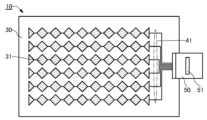
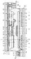
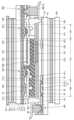
도 1의 (A)는 본 발명의 일 형태의 터치 패널(100)의 사시 개략도이다. 또한 도 1의 (B)는 도 1의 (A)를 전개한 사시 개략도이다. 또한 명료화를 위하여 대표적인 구성 요소만을 나타내었다. 또한 도 1의 (B)에서는 일부의 구성 요소(기판(30), 기판(72) 등)를 파선으로 윤곽만 명시하였다.1(A) is a schematic perspective view of a
터치 패널(100)은 입력 장치(10)와, 표시 패널(70)을 갖고, 이들이 중첩되어 제공된다.The
입력 장치(10)는 기판(30)을 갖는다. 기판(30)에는 전극(31), 전극(32), 복수의 배선(41), 복수의 배선(42)이 제공된다. 또한 기판(30)에는 복수의 배선(41) 및 복수의 배선(42)의 각각과 전기적으로 접속하는 FPC(50)가 접착되어 있다. 또한 여기서는 FPC(50) 위에 IC(51)가 제공된 예를 나타내었다.The
입력 장치(10)로서는 예를 들어 정전 용량 방식의 터치 센서를 적용할 수 있다. 이하에서는 투영형 용량 방식의 터치 센서를 적용하는 경우에 대하여 설명한다.As the
또한 이에 한정되지 않고 손가락이나 스타일러스 등의 피검지체의 근접, 또는 접촉을 검출할 수 있는 다양한 센서를 입력 장치(10)에 적용할 수 있다.In addition, it is not limited thereto, and various sensors capable of detecting the proximity or contact of a sensing object such as a finger or a stylus may be applied to the
또한 입력 장치(10)의 더 구체적인 구성에 대해서는 후술한다.A more specific configuration of the
표시 패널(70)은 대향하여 제공된 기판(71)과 기판(72)을 갖는다. 또한 기판(71) 위에는 표시부(81), 구동 회로(82), 배선(83) 등이 제공된다. 또한 기판(71)에는 배선(83)과 전기적으로 접속되는 FPC(73)가 제공된다. 또한 여기서는 FPC(73) 위에 IC(74)가 제공된 예를 나타내었다.The
표시부(81)는 화상이 표시되는 영역이며, 복수의 화소를 갖는다. 도 1의 (B)에는 표시부(81)의 일부를 확대한 개략도를 도시하였다. 화소는 적어도 하나의 표시 소자(60)를 갖는다. 또한 화소는 트랜지스터 및 표시 소자(60)를 구비하는 것이 바람직하다. 표시 소자(60)로서는 대표적으로 유기 EL 소자 등의 발광 소자나, 액정 소자 등을 이용할 수 있다.The
구동 회로(82)는, 주사선 구동 회로나 신호선 구동 회로 등의, 표시부(81)가 갖는 화소를 구동시키는 회로를 적용할 수 있다. 여기서는 구동 회로(82)로서 주사선 구동 회로를 적용하는 경우에 대하여 설명한다.As the
배선(83)은 표시부(81)나 구동 회로(82)에 신호나 전력을 전달하는 기능을 갖는다. 이 신호나 전력은 FPC(73)를 통하여 외부, 또는 IC(74)에서 배선(83)으로 입력된다.The
표시부(81)는 구동 회로(82)와 전기적으로 접속하는 복수의 주사선(게이트 선이라고도 함)(87)을 갖는다. 주사선(87)은 화소가 갖는 하나의 트랜지스터의 게이트와 전기적으로 접속하는 배선이다. 구동 회로(82)는 하나의 주사선(87)에 전기적으로 접속하는 복수의 화소를 선택하는 신호를 각 주사선(87)에 순차적으로 공급할 수 있다.The
여기서 도 1의 (B)에서는, 주사선(87)의 연장 방향을 방향(80)으로 하여 화살표로 나타내었다. 도 1의 (B)에 나타낸 구성에서는 표시부(81)의 구동 회로(82)가 제공된 측의 변(윤곽)에 직교하는 방향과 방향(80)이 평행인 경우를 도시하였다. 또한 표시부(81)의 윤곽이 장방형 또는 정방형이 아닌 경우 등에는 표시부(81)의 윤곽과 방향(80)이 직교하지 않는 경우가 있다. 또한 주사선(87)은 반드시 직선 형상일 필요는 없으며, 화소의 구성에 따라 부분적으로 만곡된 또는 굴곡진 형상이어도 좋다. 이때, 주사선(87) 위의 2개의 점을 연결하는 직선의 방향이 방향(80)에 상당한다. 또는 주사선(87)을 표시부(81)와 중첩되는 일부분에서 잘라냈을 때 이 일부분 위의 2개의 점을 연결하는 직선의 방향이 방향(80)에 상당한다. 또한 방향(80)은 하나의 주사선(87)과 전기적으로 접속하는 화소(또는 부화소)의 배열 방향에 평행한 방향이라고 바꿔 말할 수도 있다.Here, in FIG. 1(B), the extension direction of the
도 1의 (A) 및 (B)에서는 FPC(73) 위에 COF(Chip On Film) 방식에 의하여 실장된 IC(74)가 제공된 예를 도시하였다. IC(74)는 예를 들어 주사선 구동 회로, 또는 신호선 구동 회로 등으로서 기능하는 IC를 적용할 수 있다. 또한 표시 패널(70)이 주사선 구동 회로 및 신호선 구동 회로로서 기능하는 회로를 구비하는 경우나, 주사선 구동 회로나 신호선 구동 회로로서 기능하는 회로를 외부에 제공하여, FPC(73)를 통하여 표시 패널(70)을 구동하기 위한 신호를 입력하는 경우에는 IC(74)를 제공하지 않는 구성으로 하여도 좋다. 또한 IC(74)를 COG(Chip On Glass) 방식에 의하여 기판(71)에 직접 실장하여도 좋다.1 (A) and (B) show an example in which an
〔입력 장치의 구성예〕[Example of configuration of input device]
도 2의 (A)에 입력 장치(10)의 상면 개략도를 도시하였다. 입력 장치(10)는 기판(30) 위에 복수의 전극(31), 복수의 전극(32), 복수의 배선(41), 복수의 배선(42)을 갖는다. 또한 기판(30)에는 복수의 배선(41) 및 복수의 배선(42)의 각각과 전기적으로 접속하는 FPC(50)가 제공된다. 또한 도 2의 (A)에는 FPC(50)에 IC(51)가 실장된 예를 도시하였다. 또한 여기서는 구별하기 쉽게 전극(32)의 윤곽을 실선으로, 전극(31)의 윤곽을 파선으로, 각각 나타내었다.2(A) shows a schematic top view of the
도 2의 (A)에서 전극(31)은 가로 방향으로 연장하도록 배치된다. 또한 전극(32)은 전극(31)과 교차하는 방향으로 연장하도록 배치된다. 도 2의 (A)에 도시한 바와 같이 전극(31)과 전극(32)은 직교하는 방향에 제공되는 것이 바람직하다.In FIG. 2(A), the
복수의 배선(41)은 각각 하나의 전극(31)과 전기적으로 접속한다. 또한 복수의 배선(42)은 각각 하나의 전극(32)과 전기적으로 접속한다.Each of the plurality of
IC(51)는 입력 장치(10)를 구동시키기 위한 회로를 갖는다. IC(51)는 예를 들어 상호 용량 방식이나 자기 용량 방식 등의 구동 방법을 실현하는 회로를 갖는다.The
도 2의 (B)에 도 2의 (A) 중의 영역P의 확대도를 도시하였다. 전극(31)과 전극(32)은 교차부(90)에서 이들 일부가 중첩하여 서로 교차한다. 교차부(90)에서는 전극(31)과 전극(32)이 전기적으로 단락(쇼트)하지 않도록 이들 사이에 절연체가 끼여 있다.In FIG. 2(B), an enlarged view of the region P in FIG. 2(A) is shown. The
도 2의 (B)에서는 전극(32)은 국소적으로는 전극(31)을 90° 회전시킨 것과 같은 형상을 갖는 경우를 도시하였다.In (B) of FIG. 2 , the
전극(31) 및 전극(32)의 평면에서 보았을 때의 윤곽은 복수의 다이아몬드형의 패턴이 가로 방향 또는 세로 방향으로 연결되어 일체가 된 형상을 갖는다. 이때, 도 2의 (B)에 도시한 바와 같이 하나의 다이아몬드형의 패턴이 정방형이면 전극(31)의 지면 가로 방향으로 배열되는 다이아몬드형 패턴의 피치와 지면 세로 방향으로 배열되는 전극(32)의 피치를 같은 간격으로 할 수 있으므로 바람직하다. 이로써 입력 장치(10)의 검지 영역에 있어서 검출점을 같은 간격으로, 매트릭스 상으로 배치할 수 있어, 검지 정밀도를 높일 수 있다.The contours of the
전극(31)은 그 윤곽의 일부에 직선 부분(21)을 갖는다. 또한 전극(32)은 그 윤곽의 일부에 직선 부분(22)을 갖는다. 전극(31)과 전극(32)은 직선 부분(21)과 직선 부분(22)이 평행하게 대향하도록 배치된다. 이러한 구성으로 함으로써 전극(31)과 전극(32)의 간격이 일정하게 되어, 또한 이들 2개의 전극이 대향하는 길이를 길게 할 수 있다. 따라서, 2개의 전극 사이에 형성되는 용량의 크기를 크게 할 수 있다. 또한 2개의 전극이 대향하는 부분에서 2개의 전극 사이에 전위차를 주었을 때 생기는 전기력선은 밀도가 균일하게 분포되므로 장소에 따라 검출 감도에 차이가 생기는 것을 억제할 수 있다. 그러므로 검지 정밀도가 높은 터치 센서를 실현할 수 있다.
또한 도 3에 도시한 바와 같이 기판(30)에는 전극(31) 또는 전극(32) 중 한쪽만을 배치하는 구성으로 하여도 좋다. 이때, 다른 쪽의 전극을 표시 패널(70)에 제공하는 구성으로 하면 좋다. 예를 들어, 액정 소자의 코먼 전극(공통 전극)을 전극(31) 또는 전극(32)으로서 이용하면 좋다. 도 3에서는 전극(31)이 기판(30)에 배치된 구성을 도시하였지만, 전극(32)이 기판(30)에 배치된 구성으로 하여도 좋다.Further, as shown in FIG. 3, it is good also as a structure in which only one of the
도 2의 (B)에는 도 1의 (B)에 도시한 주사선(87)의 연장 방향인 방향(80)을 도시하였다. 직선 부분(21)과 직선 부분(22)이 평행일 때, 방향(80)과 직선 부분(21)이 이루는 각과 방향(80)과 직선 부분(22)이 이루는 각은 같게 된다. 여기서는 방향(80)과 직선 부분(21) 또는 직선 부분(22)이 이루는 각의 각도를 각도θ라고 표기한다. 각도θ는 30° 이상 60° 이하, 바람직하게는 40° 이상 50° 이하, 더 바람직하게는 42° 이상 48° 이하, 대표적으로는 45°인 것이 바람직하다.In FIG. 2(B), a
또한 전극(31)과 전극(32)의 간격을 D로 한다. 간격D는 작을수록 2개의 전극 사이의 용량을 높일 수 있으므로 검출 감도를 향상시킬 수 있다. 간격D의 크기로서는 예를 들어 0보다 크며 10mm 이하, 바람직하게는 1μm 이상 5mm 이하, 더 바람직하게는 3μm 이상 1mm 이하, 더욱 바람직하게는 5μm 이상 500μm 이하 등으로 하면 좋다. 또는 표시부(81)가 갖는 화소, 또는 부화소를 배열하였을 때의 피치, 또는 표시 소자(60)를 배열하였을 때의 피치의 정수배로 하는 것이 바람직하다.Further, the distance between the
도 2의 (B)에는 전극(31)과 전극(32)이 각각 격자 형상을 갖는 예를 도시하였다. 전극(31) 및 전극(32)의 격자의 간격은 그 정수배가 상기 전극(31)과 전극(32)의 간격D와 같게 되도록 설정하는 것이 바람직하다. 또한 도 2의 (B)에 도시한 바와 같이 전극(31) 및 전극(32)의 격자를 직교하는 격자로 한 경우, 격자를 이루는 2개의 직선 부분 중 하나의 방향이 직선 부분(21) 또는 직선 부분(22)과 평행이 되도록 하는 것이 바람직하다. 이때, 전극(31) 및 전극(32)이 갖는 개구부의 형상은 방향(80)에 대하여 각도θ만큼 기울어진 정방형의 형상이 된다.2(B) shows an example in which the
또한 도 2의 (B)에서는 격자의 개구부의 형상이 정방형인 경우를 도시하였지만, 이에 한정되지 않고 원형, 타원형, 각이 둥근 다각형 등, 다양한 형상으로 할 수도 있다.2(B) shows the case where the shape of the opening of the lattice is square, but it is not limited to this, and it can be made into various shapes such as circular, elliptical, and polygonal polygons with rounded angles.
전극(31) 및 전극(32)은 사용자에게 시인되지 않을 정도로 가늘게 가공되는 것이 바람직하다. 도 2의 (B)에 도시한 바와 같이 전극(31) 및 전극(32)을 격자 형상(메시 형상)으로 가공함으로써 높은 도전성과 표시 장치가 높은 시인성을 얻을 수 있다. 전극(31) 및 전극(32)의 가장 가는 부분의 폭을 30nm 이상 100μm 이하, 바람직하게는 50nm 이상 50μm 이하, 더 바람직하게는 50nm 이상 20μm 이하로 하는 것이 바람직하다. 특히 10μm 이하의 패턴 폭을 갖는 도전막은 사용자가 시인하는 것이 매우 곤란하므로 바람직하다.The
또한 전극(31) 및 전극(32)에 도전성의 나노 와이어를 사용하여도 좋다. 인접한 나노 와이어끼리가 접촉하도록 적당한 밀도로 분산함으로써 2차원적인 네트워크가 형성되어 투광성이 매우 높은 도전막으로서 기능하게 할 수 있다. 예를 들어, 직경의 평균값이 1nm 이상 100nm 이하, 바람직하게는 5nm 이상 50nm 이하, 더 바람직하게는 5nm 이상 25nm 이하의 나노 와이어를 사용할 수 있다. 나노 와이어로서 Ag 나노 와이어, Cu 나노 와이어, Al 나노 와이어 등의 금속 나노 와이어, 또는 카본 나노 튜브 등을 사용할 수 있다. 예를 들어, Ag 나노 와이어의 경우, 광투과율은 89% 이상, 시트 저항값은 40Ω/□ 이상 100Ω/□ 이하를 실현할 수 있다.Alternatively, conductive nanowires may be used for the
도 4의 (A)에 도시한 바와 같이, 전극(32)이 복수의 전극(33)과 브릿지 전극(34)에 의하여 구성되어 있어도 좋다. 여기서 전극(33)이나 브릿지 전극(34)의 상대 위치나 형상을 보기 쉽게 하기 위하여 도 4의 (B)에서는 브릿지 전극(34)만을 파선으로, 도 4의 (C)에서는 브릿지 전극(34)만을 실선으로 나타내었다. 또한 브릿지 전극(34)과 전극(31) 및 전극(33)의 상하 관계는 특별히 한정되지 않고 어느 쪽이 기판(30) 측에 배치되어도 좋다.As shown in FIG. 4(A), the
섬 형상의 전극(33)은 세로 방향으로 나란히 배치되어, 브릿지 전극(34)에 의하여 인접한 2개의 전극(33)이 전기적으로 접속한다. 이러한 구성으로 함으로써 전극(33)과 전극(31)을 동일한 도전막을 가공하여 동시에 형성할 수 있다. 그러므로 이들 막 두께나 선 폭 등의 편차를 억제할 수 있고, 각각의 전극의 저항값이 장소에 따라 편차가 생기는 것을 억제할 수 있다. 또한 이러한 구성으로 함으로써 전극(33)과 전극(31)을 동일한 평면 위에 배치할 수 있다. 따라서, 전극(31)과 전극(33)은 높이 방향의 위치의 어긋남이 생기지 않으므로 이들 사이에 생기는 전기력선의 분포를 균일하게 할 수 있어, 입력 장치(10)의 검출 감도를 향상시킬 수 있다.The island-shaped
또한 여기서는 전극(32)이 브릿지 전극(34)을 갖는 구성으로 하였지만, 전극(31)이 이러한 구성이어도 좋다. 이때, 브릿지 전극(34)을 제공함으로써 접촉 저항의 영향이 현저해지는 경우에는 전극(31)과 전극(32) 중 짧은 쪽에 브릿지 전극(34)을 갖는 구성을 적용하면 하나의 전극이 갖는 브릿지 전극(34)의 수를 줄일 수 있으므로 바람직하다.In addition, although the
도 5의 (A)에는 도 2의 (A) 중의 영역Q의 확대도를 도시하였다. 영역Q는 입력 장치(10)의 검지 영역의 모서리부를 포함하는 영역이다.Fig. 5(A) shows an enlarged view of region Q in Fig. 2(A). Area Q is an area including a corner of the detection area of the
도 5의 (A)에 도시한 바와 같이 검지 영역의 모서리부에서는 전극(31) 및 전극(32)은 방향(80)에 평행, 또는 수직인 방향에 절단한 것 같은 형상으로 하는 것이 바람직하다. 또한 전극(31) 및 전극(32)의 윤곽이 방향(80)에 평행, 또는 수직인 직선 부분을 갖는 구성으로 하면 바람직하다. 이러한 구성으로 함으로써 입력 장치(10)와 표시 패널(70)을 조합한 터치 패널(100)을 슬림 베젤화할 수 있다.As shown in FIG. 5(A), it is preferable that the
도 5의 (B)에서는 도 5의 (A)에 비해 간격D를 넓힌 경우의 예를 도시하였다. 이와 같이 전극(31)과 전극(32)의 간격을 넓힐 경우, 교차부(90)에도 격자 형상을 적용하는 것이 바람직하다. 도 5의 (B)에서는 전극(32)이 격자 형상의 브릿지 전극(34)을 갖는 경우를 도시하였다. 또한 도 2의 (B)에 도시한 바와 같이, 브릿지 전극(34)을 적용하지 않는 경우에는 전극(31) 및 전극(32)이 교차부(90)에서 격자 형상을 갖는 구성으로 하면 된다.In (B) of FIG. 5, an example of a case in which the interval D is widened compared to (A) of FIG. 5 is shown. In this way, when the distance between the
상기에서는 전극(31)과 전극(32)이 격자 형상을 갖는 경우를 나타내었지만, 이에 한정되지 않고 전극(31)과 전극(32)이 대향하는 직선 부분을 가지면 좋고, 다른 다양한 형상이 될 수 있다.In the above, the case where the
또한 도 6의 (A) 및 (B)에 도시한 바와 같이, 전극(31) 및 전극(32)은 전기적으로 절연된 더미 전극(35)을 전극(31)과 전극(32) 사이에 배치하는 구성으로 하여도 좋다. 이러한 구성으로 함으로써 전극(31)이나 전극(32)이 존재하지 않는 영역이 시인되는 것을 억제할 수 있다.In addition, as shown in (A) and (B) of FIG. 6, the
도 7의 (A)에는 도 4의 (A)에 도시한 전극(31)과 전극(33)의 다이아몬드형 전극 패턴의 안쪽을 파서 윤곽부만 남긴 형상으로 한 경우를 도시하였다. 또한 도 7의 (B)에는 전극(31)과 전극(33)으로서 격자의 한쪽의 직선 부분만 남긴 경우를 도시하였다. 또한 도 7의 (C)에는 전극(31)과 전극(33)의 안쪽에 지그재그 형상의 패턴을 갖는 경우를 나타내었다. 이때, 이 지그재그 형상의 패턴이 갖는 직선 부분은 전극(31) 또는 전극(33)이 갖는 윤곽의 직선 부분과 평행하게 되도록 형성하는 것이 바람직하다. 또한 도 7의 (C)에 도시한 바와 같이, 이 지그재그 형상의 패턴이 전극(31) 또는 전극(32)의 연장 방향을 따라 배치하면 이 방향의 전기 저항을 저감할 수 있으므로 바람직하다.FIG. 7(A) shows a case in which the inside of the diamond-shaped electrode pattern of the
또한 도 7의 (A), (B) 및 (C)에서는 전극(32)이 브릿지 전극(34)을 갖는 구성의 예를 도시하였지만, 도 2의 (B)에 도시한 바와 같이, 브릿지 전극(34)을 적용하지 않는 구성으로 하여도 좋다.7 (A), (B) and (C) show an example of a configuration in which the
도 2의 (A) 등에서는 전극(31) 및 전극(32)의 상면 형상으로서, 복수의 다이아몬드형이 한 방향으로 연결된 형상이 된 예를 도시하였지만, 전극(31) 및 전극(32)의 형상은 이에 한정되지 않고 띠 모양(장방형 형상), 곡선을 갖는 띠 모양, 지그재그 형상 등, 다양한 상면 형상으로 할 수 있다. 또한 상기에서는 전극(31)과 전극(32)이 직교하도록 배치된 것 같이 도시하였지만 이들은 반드시 직교하여 배치될 필요는 없고 2개의 전극이 이루는 각의 각도가 90° 미만이라도 좋다.2(A) and the like show an example in which a plurality of diamond shapes are connected in one direction as the upper surface shapes of the
도 8의 (A)에서는 지그재그 형상의 상면 형상을 갖는 전극(36) 및 전극(37)을 이용한 경우의 예를 도시하였다. 또한 명료화를 위하여 도 8의 (A) 등에서는 전극(36)을 파선으로, 전극(37)을 실선으로 나타내었다. 이때, 도 8의 (A)에서 도시한 바와 같이, 각각의 직선 부분의 중심 위치를 중첩시키는 게 아니라 상대적으로 어긋나게 배치하는 것이 바람직하다. 이로써 전극(36)과 전극(37)이 평행하게 대향하는 부분을 접근시킬 수 있고, 전극 사이에 용량이 높아져 검출 감도가 향상되므로 바람직하다. 또는 도 8의 (B)에 도시한 바와 같이, 전극(36) 및 전극(37)의 상면 형상을 지그재그 형상의 직선 부분의 일부가 돌출한 형상으로 하면, 이 직선 부분의 중심 위치를 중첩하여 배치하여도 대향하는 부분의 길이를 길게 할 수 있으므로 전극 사이에 용량을 높일 수 있다.In (A) of FIG. 8, an example of using
도 8의 (A) 중의 일점쇄선으로 둘러싼 영역의 확대도를 도 9의 (A)에, 도 8의 (B) 중의 일점쇄선으로 둘러싼 영역의 확대도를 도 9의 (D)에 각각 도시하였다. 또한 각 도면에는 전극(36), 전극(37) 및 이들이 교차하는 교차부(38)를 도시하였다. 여기서 도 9의 (B) 및 (E)에 도시한 바와 같이, 도 9의 (A) 및 (D)에서의 전극(36) 및 전극(37)의 직선 부분이 모서리부를 갖도록 사행하는 형상이어도 좋고, 도 9의 (C) 및 (F)에 도시한 바와 같이, 곡선이 연속하도록 사행하는 형상이어도 좋다.An enlarged view of the region surrounded by the dashed-dotted line in Fig. 8(A) is shown in Fig. 9(A), and an enlarged view of the region surrounded by the dashed-dotted line in Fig. 8(B) is shown in Fig. 9(D), respectively. . In addition, each drawing shows an
이상의 내용이 입력 장치의 구성예에 대한 설명이다.The above is a description of the configuration example of the input device.
〔화소의 구성예〕[Example of configuration of pixel]
이하에서는 본 발명의 일 형태의 터치 패널(100)이 갖는 표시 패널(70)의 화소의 구성예에 대하여 설명한다.Hereinafter, an example of a configuration of pixels of the
상술한 바와 같이, 표시 패널(70)의 표시부에는 복수의 화소가 제공된다. 또한 화소는 하나 이상의 표시 소자(60)를 갖는다. 풀 컬러의 화상을 표시하는 표시 패널(70)로 하는 경우, 예를 들어 하나의 화소에 적색(R), 녹색(G), 청색(B)의 3색의 표시 소자(60)가 제공된 구성으로 하는 것이 바람직하다. 또한 하나의 화소가 상기 3색에 더하여 황색(Y)이나 백색(W)의 표시 소자(60)를 갖는 구성으로 하면, 소비 전력을 저감할 수 있으므로 바람직하다. 여기서 하나의 표시 소자(60)와 이에 대응하는 화소 회로를 갖는 구성을 부화소라고 부를 경우도 있다. 화소가 3개의 표시 소자(60)를 갖는 경우 화소는 3개의 부화소를 포함하는 구성으로 할 수 있다.As described above, a plurality of pixels are provided in the display portion of the
또한 입력 장치(10)를 표시 패널(70)에 중첩하여 배치하는 경우, 입력 장치(10)가 갖는 전극(31) 및 전극(32)이 표시 소자(60)의 사이에 위치하도록 배치하는 것이 바람직하다. 이로써 표시 소자(60)에서의 광이 전극(31) 및 전극(32)에 의하여 차단되는 일이 없으므로 입력 장치(10)를 제공하였을 때의 표시 패널(70)의 휘도의 저하를 실질적으로 없애거나 또는 매우 작게 할 수 있다. 따라서, 시인성이 높고, 또한 소비 전력이 저감된 터치 패널을 실현할 수 있다. 또한 전극(31) 및 전극(32)이 표시 소자(60)와 중첩되지 않으므로 전극(31) 및 전극(32)에 비교적 저항이 큰 투광성의 도전체 재료를 사용할 필요가 없다. 그러므로 전극(31) 및 전극(32)에 저항이 작은 금속이나 합금 재료를 사용할 수 있고 전극(31)이나 전극(32)을 육안으로 시인할 수 없을 정도로까지 매우 가늘게 형성할 수 있다. 따라서, 전극(31)이나 전극(32)이 광을 반사하거나 하여 시인되는 것도 억제할 수 있으므로, 더 시인성이 높은 터치 패널을 실현할 수 있다.In addition, when the
도 10에 도 1의 (A)에 도시한 터치 패널(100)의 표시면 측에서 보았을 때의 표시부(81)와, 입력 장치(10)를 중첩한 상태에 있어서의 확대도를 도시하였다. 여기서는 표시 패널(70)이 갖는 화소(40)가 상이한 색을 나타내는 4개의 표시 소자(60)(표시 소자(60R), 표시 소자(60G), 표시 소자(60B), 표시 소자(60Y))를 갖는 경우에 대하여 나타내었다. 또한 이하에서 4종류의 표시 소자에 공통된 사항을 설명할 때 표시 소자(60)라고 표기하여 설명한다.FIG. 10 is an enlarged view in a state where the
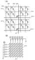
도 10에는 전극(31)과 각 표시 소자(60)의 위치 관계를 도시하였다. 또한 여기서는 전극(31)을 나타내었지만, 전극(32)(또는 전극(33) 및 브릿지 전극(34))의 경우도 마찬가지이다. 또한 도 10에는 표시 패널(70)이 갖는 주사선(87)의 방향을 설명하기 위하여 3개의 주사선(주사선(87a), 주사선(87b), 주사선(87c))을 파선으로 나타내고, 또한 주사선의 연장 방향인 방향(80)도 나타내었다.10 shows the positional relationship between the
도 10에 도시한 구성에서는 전극(31)이 갖는 격자의 직선 부분과 주사선(87)이 이루는 각의 각도가 45°인 경우를 나타내었다. 표시 소자(60)는 전극(31)이 갖는 직선 부분을 따라 배열된다. 여기서, 도 10에서 비스듬하게 배열되는 복수의 표시 소자(60)는 상이한 2색에 대응하는 2종류의 표시 소자(60)가 번갈아 배열된다. 하나의 화소(40)는 인접한 4개의 표시 소자(60)(표시 소자(60R), 표시 소자(60G), 표시 소자(60B), 표시 소자(60Y))를 포함하여 구성된다. 여기서 표시 소자(60R)는 적색을 나타내는 표시 소자이고, 표시 소자(60G)는 녹색을 나타내는 표시 소자이고, 표시 소자(60B)는 청색을 나타내는 표시 소자이고, 표시 소자(60Y)는 황색을 나타내는 표시 소자로 한다.In the configuration shown in FIG. 10, the case where the angle formed by the linear portion of the lattice of the
하나의 표시 소자(60)는 그 윤곽이 전극(31)이 갖는 격자의 직선 부분에 평행한 부분을 갖는 것이 바람직하다. 이러한 형상으로 함으로써 표시 소자(60)를 배열할 때의 2개의 표시 소자(60)의 틈을 적게 하여 개구율을 높일 수 있다. 도 10에서는 표시 소자(60)의 윤곽이 모서리부가 둥근 사각형상으로 하였지만 이에 한정되지 않고 정방형, 장방형, 다각형, 타원형, 원형, 또는 모서리부가 둥근 다각형 등의 형상으로 하여도 좋다.One
도 10에서 나타낸 주사선(87a)은 예를 들어 표시 소자(60R)를 포함하는 부화소를 구동하는 주사선에 대응한다. 또한 주사선(87b)은 표시 소자(60G)를 포함하는 부화소, 및 표시 소자(60Y)를 포함하는 부화소를 구동하는 주사선에 대응한다. 또한 주사선(87c)은 표시 소자(60B)를 포함하는 부화소를 구동하는 주사선에 대응한다. 각 주사선은 각 부화소에 포함되는 트랜지스터의 게이트와 전기적으로 접속한다. 즉, 도 10에서 예시하는 구성에서는, 하나의 화소는 3개의 주사선(87)에 의하여 구동할 수 있다.A
도 10에서는 전극(31)이 갖는 개구부 중 하나에, 하나의 화소(40)(즉, 4개의 표시 소자(60))가 포함되는 구성을 도시하였지만 이에 한정되지 않고 전극(31)은 인접한 표시 소자(60) 사이에 배치되도록 가공된 다양한 형태가 될 수 있다.Although FIG. 10 shows a configuration in which one pixel 40 (ie, four display elements 60) is included in one of the openings of the
도 11의 (A)에는 전극(31)이 갖는 격자의 개구부에 하나의 표시 소자(60)가 포함되도록 배치한 경우를 도시하였다. 또한 도 11의 (B)에는 전극(31)이 스트라이프 형상인 경우를 도시하였다. 또한 도 11의 (C)에서는 전극(31)이 갖는 격자의 하나의 개구부에 복수의 화소(40)가 배치된 예를 도시하였다. 또한 도 11의 (D)에서는 전극(31)이 갖는 격자에서 직교하는 2개의 방향의 격자의 피치가 상이한 경우를 도시하였다. 또한 도 11의 (E) 및 도 11의 (F)에는 도 7의 (C)에 도시한 바와 같이, 전극(31)이 지그재그 형상을 갖는 경우의 예를 나타내었다.11(A) shows a case where one
또한 도 10 및 도 11에서는 하나의 화소(40)에 4색의 표시 소자(60)가 제공된 예를 도시하였지만, 이에 한정되지 않고 3색, 또는 5색 이상의 표시 소자를 제공하여도 좋다.In addition, FIGS. 10 and 11 show an example in which the
도 12에서는 하나의 화소(40)가 3색의 표시 소자(60)를 갖는 경우의 예를 도시하였다. 도 12에서는 설명을 용이하게 하기 위하여, 화소(40a), 화소(40b), 및 화소(40c)를 다른 화소와 구별해서 도시하고, 화소(40a), 화소(40b), 및 화소(40c) 각각에 포함되는 3개의 표시 소자(60)에 같은 해치 패턴을 부여하였다.12 illustrates an example in which one
도 12에서 세로 방향으로 배열된 화소(40a)와 화소(40b)는, 이에 포함되는 3 개의 표시 소자(60)의 배열이 같다. 또한 가로 방향으로 배열된 화소(40a)와 화소(40c)는, 각각 표시 소자(60)의 상하가 역전되어 배열되어 있다.In FIG. 12 , the three
또한 도 12에서는 지면 세로 방향으로 동일한 색의 표시 소자(60)가 배열된다. 이러한 구성으로 함으로써 컬러 필터나 발광 소자를 상이한 색의 표시 소자(60)에 따라 나누어 만들 때에 형성하기 쉬워지므로 바람직하다.Also, in FIG. 12 ,
도 13의 (A)에는 하나의 화소가 3색의 표시 소자(60)를 갖는 경우의 예를 도시하였다. 표시 소자(60)는 그 윤곽이 전극(31)의 격자의 방향에 따른 직선 부분을 갖고, 모서리부의 둥근 장방형의 형상을 갖는 예를 나타내었다. 또한 같은 색의 표시 소자(60)가 전극(31)의 격자의 방향을 따라 배열되어 스트라이프 배치를 형성한다. 또한 도 13의 (B)~(D)에는 전극(31)이 도 13의 (A)와 상이한 형상으로 배치된 예를 도시하였다.13(A) shows an example in which one pixel has the
또한 도 10~도 13에서는 설명을 용이하게 하기 위하여 복수의 표시 소자(60) 중 몇 개에 R,G,B,Y 등의 부호를 부여하였지만 이 배치 방법은 일례이며 표시 소자(60)의 배치 방법을 한정하는 것이 아니다. R,G,B,Y는 서로 교환할 수 있다. 또한 R,G,B,Y의 어느 하나를 대신하여 백색의 표시 소자에 대응하는 W를 배치하여도 좋다.In addition, in FIGS. 10 to 13, some of the plurality of
이상의 내용이 화소의 구성예에 대한 설명이다.The above is an explanation of a configuration example of a pixel.
[단면 구성예][Example of section structure]
이하에서는 터치 패널(100)의 단면 구성의 예에 대하여 도면을 참조하여 설명한다.Hereinafter, an example of a cross-sectional configuration of the
〔단면 구성예 1〕[Cross-section configuration example 1]
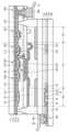
도 14는 터치 패널(100)의 단면 개략도이다. 도 14에서는 도 1의 (A)에서의 FPC(73)를 포함하는 영역, 구동 회로(82)를 포함하는 영역, 표시부(81)를 포함하는 영역, 및 FPC(50)를 포함하는 영역의 각각의 단면도를 도시하였다.14 is a schematic cross-sectional view of the
기판(71)과 기판(72)은 접착층(151)에 의하여, 또한 기판(72)과 기판(30)은 접착층(152)에 의하여 접합되어 있다. 여기서 기판(71)과 기판(72) 및 그 사이에 끼이는 구성 요소를 포함하는 구성이 표시 패널(70)에 상당한다. 또한 기판(30) 및 기판(30) 위에 제공된 구성 요소를 포함하는 입력 장치(10)에 상당한다.The
<표시 패널(70)><
기판(71)과 기판(72) 사이에는 트랜지스터(201), 트랜지스터(202), 트랜지스터(203), 표시 소자(60), 용량 소자(205), 접속부(206), 배선(207) 등이 제공된다.A
기판(71) 위에는 절연층(211), 절연층(212), 절연층(213), 절연층(214), 절연층(215), 스페이서(216) 등이 제공된다. 절연층(211)은 그 일부가 각 트랜지스터의 게이트 절연층으로서 기능하고, 또한 다른 일부가 용량 소자(205)의 유전체로서의 기능을 갖는다. 절연층(212), 절연층(213), 및 절연층(214)은 각 트랜지스터나 용량 소자(205) 등을 덮도록 제공된다. 절연층(214)은 평탄화층으로서의 기능을 갖는다. 또한 여기서 트랜지스터를 덮는 절연층으로서 절연층(212), 절연층(213), 및 절연층(214)의 3층을 갖는 경우를 나타내었지만 이에 한정되지 않고 4층 이상이어도 좋고, 단층, 또는 2층이어도 좋다. 또한 평탄화층으로서 기능하는 절연층(214)은 필요가 없으면 제공하지 않아도 된다.An insulating
절연층(214) 위에 표시 소자(60)가 제공되어 있다. 여기서는 표시 소자(60)로서 상면 사출형(톱 에미션형)의 발광 소자(유기 EL 소자)를 적용한 경우의 예를 나타내었다. 표시 소자(60)는 제 2 전극(223) 측에 광을 사출한다. 표시 소자(60)의 발광 영역과 중첩하여 트랜지스터(202), 트랜지스터(203), 용량 소자(205), 및 배선 등을 배치함으로써 표시부(81)의 개구율을 높일 수 있다.A
표시 소자(60)는 제 1 전극(221)과 제 2 전극(223) 사이에 EL층(222)을 갖는다. 또한 제 1 전극(221)과 EL층(222) 사이에는 광학 조정층(224)이 제공된다. 절연층(215)은 제 1 전극(221)과 광학 조정층(224)의 단부를 덮도록 제공되어 있다.The
도 14에서는 표시부(81)의 예로서 1 화소분의 단면을 도시하였다. 여기서 화소가 전류 제어용 트랜지스터(202)와 스위칭 제어용의 트랜지스터(203)와 용량 소자(205)를 갖는 경우를 나타내었다. 트랜지스터(202)의 소스 또는 드레인 중 한쪽, 및 용량 소자(205)의 한쪽의 전극은 절연층(212), 절연층(213) 및 절연층(214)에 제공된 개구부를 통하여 제 1 전극(221)과 전기적으로 접속한다.14 shows a cross section of one pixel as an example of the
또한 도 14에는 구동 회로(82)의 예로서 트랜지스터(201)가 제공된 구성을 도시하였다.14 shows a configuration in which a
트랜지스터(201), 트랜지스터(202), 및 트랜지스터(203)는 각각 게이트 전극으로서 기능하는 도전층(241)과, 반도체층(242)과, 한쪽이 소스 전극으로서 기능하고, 다른 쪽이 드레인 전극으로서 기능하는 한 쌍의 도전층(243)과, 게이트 절연층으로서 기능하는 절연층(211)을 갖는다.The
도 14에서는 트랜지스터(201) 및 트랜지스터(202)에 채널이 형성되는 반도체층을 2개의 게이트 전극(도전층(241) 및 도전층(244)) 사이에 개재(介在)하는 구성을 적용한 예를 도시하였다. 이러한 트랜지스터는 다른 트랜지스터와 비교하여 전계 효과 이동도를 높일 수 있고, 온 전류를 증대시킬 수 있다. 그 결과, 고속 동작이 가능한 회로를 제작할 수 있다. 더구나 회로의 점유 면적을 축소시킬 수 있다. 온 전류가 큰 트랜지스터를 적용함으로써 표시 패널을 대형화, 또는 고정세(高精細)화하였을 때 배선수가 증대하여도, 각 배선에서의 신호 지연을 저감할 수 있고, 표시의 휘도의 편차를 저감할 수 있다.14 shows an example in which a semiconductor layer in which channels are formed in the
또한 구동 회로(82)와 표시부(81)에 제공되는 트랜지스터는 각각 같은 구조의 트랜지스터로 하여도 좋고, 상이한 구조의 트랜지스터를 조합하여 사용하여도 좋다.Transistors provided in the
각 트랜지스터를 덮는 절연층(212), 절연층(213) 중 적어도 한쪽은 물이나 수소 등의 불순물이 확산되기 어려운 재료를 사용하는 것이 바람직하다. 즉, 절연층(212) 또는 절연층(213)은 배리어막으로서 기능시킬 수 있다. 이러한 구성으로 함으로써 트랜지스터에 대하여 외부로부터 불순물이 확산되는 것을 효과적으로 억제할 수 있어, 신뢰성이 높은 터치 패널을 실현할 수 있다.At least one of the insulating
스페이서(216)는 절연층(215) 위에 제공되어, 기판(71)과 기판(72)의 거리를 조정하는 기능을 갖는다. 도 14에서 스페이서(216)와 차광층(232) 사이에 틈이 있는 경우를 도시하였지만 이들이 접하여도 좋다. 또한 여기서는 스페이서(216)를 기판(71) 측에 제공한 구성을 나타내었지만 기판(72) 측(예를 들어 차광층(232)보다 기판(71) 측)에 제공하여도 좋다. 또는 스페이서(216)를 대신하여 입자상의 스페이서를 사용하여도 좋다. 입자상의 스페이서로서 실리카 등의 재료를 사용할 수도 있지만 유기 수지나 고무 등의 탄성을 갖는 재료를 사용하는 것이 바람직하다. 이때, 입자상의 스페이서는 상하 방향에 찌부러진 형상이 되는 경우가 있다.The
기판(72)의 기판(71) 측에는 착색층(231), 차광층(232) 등이 제공되어 있다. 차광층(232)은 개구를 갖고, 이 개구가 표시 소자(60)의 표시 영역과 중첩되도록 배치된다. 착색층(231)은 표시 소자(60)와 중첩하도록 제공되어 있다.On the
차광층(232)으로서 사용할 수 있는 재료로서는, 카본 블랙, 금속 산화물, 복수의 금속 산화물의 고용체를 포함하는 복합 산화물 등을 들 수 있다. 또한 차광층(232)에 착색층(231)의 재료를 포함하는 막의 적층막을 사용할 수도 있다. 예를 들어, 착색층(231)에 아크릴 수지를 포함하는 재료를 사용하여, 어떤 색의 광을 투과하는 착색층에 사용하는 재료를 포함하는 막과 다른 색의 광을 투과하는 착색층에 사용하는 재료를 포함하는 막과의 적층 구조를 사용할 수 있다. 착색층(231)과 차광층(232)의 재료를 공통으로 함으로써 장치를 공통화할 수 있고, 또한 공정을 간략화할 수 있으므로 바람직하다.Examples of materials that can be used for the
예를 들어, 착색층(231)에 사용할 수 있는 재료로서, 금속 재료, 수지 재료, 안료, 또는 염료가 포함된 수지 재료 등을 들 수 있다.For example, materials usable for the
또한 착색층(231) 및 차광층(232)을 덮어서 오버 코트로서 기능하는 절연층을 제공하여도 좋다.In addition, an insulating layer may be provided that covers the
기판(71)의 단부에 가까운 영역에 접속부(206)가 제공되어 있다. 접속부(206)는 접속층(209)을 통하여 FPC(73)가 전기적으로 접속되어 있다. 도 14에 도시한 구성에는 구동 회로(82)와 전기적으로 접속하는 배선(207)의 일부와 제 1 전극(221)과 동일한 도전막을 가공하여 형성된 도전층을 적층하여, 접속부(206)를 구성하는 예를 나타내었다. 이와 같이 2개 이상의 도전층을 적층하여 접속부(206)를 구성함으로써 전기 저항을 저감할 수 있을 뿐만 아니라 접속부(206)의 기계적 강도를 높일 수 있다.A
또한 도 14에는 일례로서 트랜지스터의 게이트 전극과 동일한 도전막을 가공하여 형성된 배선과 트랜지스터의 소스 전극 및 드레인 전극과 동일한 도전막을 가공하여 형성된 배선이 교차하는 교차부(86)의 단면 구조를 도시하였다.As an example, FIG. 14 shows a cross-sectional structure of an
여기서는 교차부(86)에 트랜지스터의 게이트 전극과 동일한 도전막을 가공하여 형성된 주사선(87)이 제공된 경우를 나타내었다. 또한 주사선(87)은 트랜지스터의 소스 전극 및 드레인 전극과 동일한 도전막을 가공하여 형성된 배선이어도 좋고, 다른 도전막을 사용하여도 좋다.Here, a case where a
<입력 장치(10)><Input Device (10)>
기판(30)의 기판(72) 측에는 전극(31) 및 전극(32)이 제공되어 있다. 여기서는 전극(31)이 전극(33) 및 브릿지 전극(34)을 갖는 경우의 예를 나타내었다. 도 14 중의 교차부(86)에 도시한 바와 같이, 전극(32)과 전극(33)은 동일 평면 위에 형성되어 있다. 또한 전극(32) 및 전극(33)을 덮는 절연층(161) 위에 브릿지 전극(34)이 제공되어 있다. 브릿지 전극(34)은 절연층(161)에 제공된 개구를 통하여 전극(32)을 끼우도록 제공되는 2개의 전극(33)과 전기적으로 접속되어 있다.An
또한 도 14에 도시한 구성에서는 전극(33)이 표시 소자(60)와 중첩되지 않도록 배치되어 있는 예를 도시하였다. 즉, 전극(33)이 갖는 개구와 표시 소자(60)가 중첩되도록 전극(33)이 배치되어 있다. 이때, 전극(33)은 착색층(231)과도 중첩되지 않도록 배치하는 것이 바람직하다. 또한 전극(33)은 차광층(232)과 중첩되도록 배치하는 것이 바람직하다. 또한 여기서는 전극(33)의 예를 나타내었지만, 전극(31), 전극(32) 및 브릿지 전극(34)도 마찬가지로 표시 소자(60)와 중첩되지 않도록 배치되어 있는 것이 바람직하다.In the configuration shown in FIG. 14 , an example in which the
기판(30)의 단부에 가까운 영역에는 접속부(106)가 제공되어 있다. 접속부(106)는 접속층(109)을 통하여 FPC(50)가 전기적으로 접속되어 있다. 도 14에 도시한 구성에서는 배선(42)의 일부와 브릿지 전극(34)이 동일한 도전막을 가공하여 얻어진 도전층을 적층하여 접속부(106)를 구성하는 예를 나타내었다.A
접속층(109)이나 접속층(209)으로서는 이방성 도전 필름(ACF:Anisotropic Conductive Film)이나 이방성 도전 페이스트(ACP:Anisotropic Conductive Paste) 등을 사용할 수 있다.As the
여기서 기판(30)은 손가락 또는 스타일러스 등의 피검지체가 직접 접촉되는 기판으로서도 사용할 수 있다. 이 경우, 기판(30) 위에 보호층(세라믹 코트 등)을 제공할 수 있다. 보호층은 예를 들어 산화 실리콘, 산화 알루미늄, 산화 이트륨, 이트리아 안정화 지르코니아(YSZ) 등의 무기 절연 재료를 사용할 수 있다. 또한 기판(30)에 강화 유리를 사용하여도 좋다. 강화 유리는 이온 교환법이나 풍랭 강화법 등에 의하여 물리적, 또는 화학적인 처리가 수행되어 그 표면에 압축 응력을 가한 것을 사용할 수 있다. 터치 센서를 강화 유리의 한쪽 면에 제공하고, 그 반대쪽 면을 예를 들어 전자 기기의 가장 바깥쪽에 제공하여 터치면으로서 사용함으로써 기기 전체의 두께를 저감할 수 있다.Here, the
<각 구성 요소에 대하여><About each component>
이하에서는 상술한 각 구성 요소에 대하여 설명한다.Hereinafter, each component described above will be described.
터치 패널이 갖는 기판에는 평탄면을 갖는 재료를 사용할 수 있다. 표시 소자로부터의 광을 추출하는 측의 기판에는 이 광을 투과하는 재료를 사용한다. 예를 들어, 유리, 석영, 세라믹, 사파이어, 유기 수지 등의 재료를 사용할 수 있다.A material having a flat surface can be used for a substrate included in the touch panel. A material that transmits this light is used for the substrate on the side for extracting the light from the display element. For example, materials such as glass, quartz, ceramics, sapphire, and organic resins can be used.
두께가 얇은 기판을 사용함으로써 터치 패널의 경량화, 박량화를 도모할 수 있다. 또한 가요성을 가질 정도의 두께의 기판을 사용함으로써 가요성을 갖는 터치 패널을 실현할 수 있다.By using a substrate having a thin thickness, the touch panel can be reduced in weight and reduced in weight. In addition, a touch panel having flexibility can be realized by using a substrate having a thickness sufficient to have flexibility.
유리로서는 예를 들어, 무 알칼리 유리, 바륨 보로실리케이트 유리, 알루미노 보로실리케이트 유리 등을 사용할 수 있다.As glass, alkali free glass, barium borosilicate glass, alumino borosilicate glass, etc. can be used, for example.
가요성 및 가시광에 대한 투과성을 갖는 재료로서는 예를 들어, 가요성을 가질 정도의 두께의 유리나 폴리에틸렌테레프탈레이트(PET), 폴리에틸렌나프탈레이트(PEN) 등의 폴리에스테르 수지, 폴리아크릴로나이트릴 수지, 폴리이미드 수지, 폴리메틸메타크릴레이트 수지, 폴리카보네이트(PC) 수지, 폴리에터설폰(PES) 수지, 폴리아마이드 수지, 사이클로올레핀 수지, 폴리스타이렌 수지, 폴리아마이드이미드 수지, 폴리염화바이닐 수지, 폴리테트라플루오로에틸렌(PTFE) 수지 등을 들 수 있다. 특히 열팽창 계수가 낮은 재료를 사용하는 것이 바람직하여, 예를 들어 폴리아마이드이미드 수지, 폴리이미드 수지, PET 등을 적합하게 사용할 수 있다. 또한 유리 섬유에 유기 수지를 함침(含浸)시킨 기판이나 무기 필러를 유기 수지에 섞어 열팽창 계수를 낮춘 기판을 사용할 수도 있다. 이러한 재료를 사용한 기판은 중량이 가벼우므로 이 기판을 사용한 터치 패널도 경량으로 할 수 있다.Examples of materials having flexibility and transparency to visible light include glass having a thickness sufficient to have flexibility, polyester resins such as polyethylene terephthalate (PET) and polyethylene naphthalate (PEN), polyacrylonitrile resins, Polyimide resin, polymethyl methacrylate resin, polycarbonate (PC) resin, polyethersulfone (PES) resin, polyamide resin, cycloolefin resin, polystyrene resin, polyamideimide resin, polyvinyl chloride resin, polytetra A fluoroethylene (PTFE) resin etc. are mentioned. In particular, it is preferable to use a material having a low coefficient of thermal expansion, and for example, polyamideimide resin, polyimide resin, PET, etc. can be suitably used. In addition, a substrate in which glass fibers are impregnated with an organic resin or a substrate in which an organic resin is mixed with an inorganic filler and the coefficient of thermal expansion is lowered may be used. Since a substrate using such a material is light in weight, a touch panel using this substrate can also be made lightweight.
또한 발광을 추출하지 않는 측의 기판은 투광성을 갖지 않아도 되므로 상술한 기판 외에 금속 기판, 세라믹 기판, 또는 반도체 기판을 사용할 수도 있다. 금속 기판은 열 전도성이 높고, 금속 기판 전체에 열을 용이하게 전도할 수 있으므로 터치 패널의 국소적인 온도 상승을 억제할 수 있어, 바람직하다. 가요성이나 굽힘성을 얻기 위해서는 금속 기판의 두께는 10μm 이상 200μm 이하가 바람직하고, 20μm 이상 50μm 이하인 것이 더 바람직하다.Also, since the substrate on the side from which light emission is not extracted does not have to have light-transmitting properties, a metal substrate, a ceramic substrate, or a semiconductor substrate may be used in addition to the above-described substrate. A metal substrate is preferable because it has high thermal conductivity and can easily conduct heat throughout the metal substrate, thereby suppressing a local temperature rise of the touch panel. In order to obtain flexibility and bendability, the thickness of the metal substrate is preferably 10 μm or more and 200 μm or less, more preferably 20 μm or more and 50 μm or less.
금속 기판을 구성하는 재료는 특별히 한정되지 않지만 예를 들어 알루미늄, 구리, 니켈 등의 금속, 또는 알루미늄 합금 또는 스테인리스 등의 합금 등을 적합하게 사용할 수 있다.Although the material constituting the metal substrate is not particularly limited, for example, a metal such as aluminum, copper, or nickel, or an alloy such as aluminum alloy or stainless steel can be suitably used.
또한 금속 기판의 표면을 산화시키거나, 표면에 절연막을 형성함으로써 절연 처리가 수행된 기판을 사용하여도 좋다. 예를 들어, 스핀 코팅법이나 딥법(dipping method) 등의 도포법, 전착법, 증착법 또는 스퍼터링법 등을 이용하여 절연막을 형성하여도 좋고, 산소 분위기에서 방치하거나 가열하는 외에 양극 산화법 등에 의하여 기판의 표면에 산화막을 형성하여도 좋다.Alternatively, a substrate on which an insulation treatment has been performed by oxidizing the surface of the metal substrate or forming an insulating film on the surface may be used. For example, an insulating film may be formed using a coating method such as spin coating or dipping method, electrodeposition method, vapor deposition method, sputtering method, or the like. An oxide film may be formed on the surface.
가요성을 갖는 기판에 터치 패널의 표면을 손상 등으로부터 보호하는 하드 코트층(예를 들어, 질화 실리콘층 등)이나, 압력을 분산할 수 있는 재질의 층(예를 들어, 아라미드 수지층 등) 등이 적층되어도 좋다. 또한 수분 등으로 인한 표시 소자의 수명 저하 등을 억제하기 위하여 가요성을 갖는 기판에 투수성이 낮은 절연막이 형성되어도 좋다. 예를 들어, 질화 실리콘막, 산화 질화 실리콘막 등의 질소와 실리콘을 포함하는 막이나, 질화 알루미늄막 등의 질소와 알루미늄을 포함하는 투수성이 낮은 절연막을 가져도 좋다.A hard coat layer (eg, silicon nitride layer, etc.) that protects the surface of the touch panel from damage on a substrate having flexibility, or a layer made of a material capable of distributing pressure (eg, an aramid resin layer, etc.) etc. may be laminated. In addition, an insulating film having low water permeability may be formed on the substrate having flexibility in order to suppress a decrease in life of the display element due to moisture or the like. For example, a film containing nitrogen and silicon, such as a silicon nitride film or a silicon oxynitride film, or an insulating film containing nitrogen and aluminum, such as an aluminum nitride film, may be provided.
기판은 복수의 층을 적층하여 사용할 수도 있다. 특히 유리층을 갖는 구성으로 하면 물이나 산소에 대한 배리어성을 향상시키고, 신뢰성이 높은 터치 패널로 할 수 있다.The substrate may be used by laminating a plurality of layers. In particular, when the structure has a glass layer, barrier properties to water and oxygen can be improved, and a highly reliable touch panel can be obtained.
예를 들어, 표시 소자에 가까운 측에서 유리층, 접착층, 및 유기 수지층을 적층한 기판을 사용할 수 있다. 이 유리층의 두께는 20μm 이상 200μm 이하, 바람직하게는 25μm 이상 100μm 이하로 한다. 이러한 두께의 유리층은 물이나 산소에 대한 높은 배리어성과 가요성을 동시에 실현할 수 있다. 또한 유기 수지층의 두께는 10μm 이상 200μm 이하, 바람직하게는 20μm 이상 50μm 이하로 한다. 이러한 유기 수지층을 유리층보다 외측에 제공함으로써 유리층의 깨짐이나 크랙을 억제하여, 기계적 강도를 향상시킬 수 있다. 이러한 유리 재료와 유기 수지의 복합 재료를 기판에 적용함으로써 극히 신뢰성이 높은 플렉시블한 터치 패널로 할 수 있다.For example, a substrate in which a glass layer, an adhesive layer, and an organic resin layer are laminated on the side close to the display element can be used. The thickness of this glass layer is 20 μm or more and 200 μm or less, preferably 25 μm or more and 100 μm or less. A glass layer having such a thickness can realize high barrier properties against water or oxygen and flexibility at the same time. In addition, the thickness of the organic resin layer is 10 μm or more and 200 μm or less, preferably 20 μm or more and 50 μm or less. By providing such an organic resin layer outside the glass layer, cracks and cracks of the glass layer can be suppressed, and mechanical strength can be improved. By applying such a composite material of a glass material and an organic resin to a substrate, a highly reliable flexible touch panel can be obtained.
트랜지스터는 게이트 전극으로서 기능하는 도전층과, 반도체층과, 소스 전극으로서 기능하는 도전층과, 드레인 전극으로서 기능하는 도전층과, 게이트 절연층으로서 기능하는 절연층을 갖는다.A transistor has a conductive layer functioning as a gate electrode, a semiconductor layer, a conductive layer functioning as a source electrode, a conductive layer functioning as a drain electrode, and an insulating layer functioning as a gate insulating layer.
또한 본 발명의 일 형태의 터치 패널이 갖는 트랜지스터의 구조는 특별히 한정되지 않는다. 예를 들어, 스태거형의 트랜지스터로 하여도 좋고, 역 스태거형의 트랜지스터로 하여도 좋다. 또한, 톱 게이트형 또는 보텀 게이트형 중 어느 트랜지스터 구조로 하여도 좋다. 트랜지스터에 사용하는 반도체 재료는 특별히 한정되지 않고, 예를 들어 산화물 반도체, 실리콘, 저마늄, 유기 반도체 등을 들 수 있다.In addition, the structure of the transistor included in the touch panel of one embodiment of the present invention is not particularly limited. For example, it may be a staggered transistor or an inverted staggered transistor. In addition, it is good also as a transistor structure of either a top-gate type or a bottom-gate type. The semiconductor material used for the transistor is not particularly limited, and examples thereof include oxide semiconductors, silicon, germanium, and organic semiconductors.
트랜지스터에 사용하는 반도체 재료의 결정성에 대해서도 특별히 한정되지 않고, 비정질 반도체, 결정성을 갖는 반도체(미결정 반도체, 다결정 반도체, 단결정 반도체, 또는 일부에 결정 영역을 갖는 반도체) 중 어느 것을 사용하여도 좋다. 결정성을 갖는 반도체를 사용하면 트랜지스터 특성의 열화를 억제할 수 있으므로 바람직하다.The crystallinity of the semiconductor material used for the transistor is not particularly limited, and either an amorphous semiconductor or a crystalline semiconductor (a microcrystal semiconductor, a polycrystalline semiconductor, a single crystal semiconductor, or a semiconductor having a crystalline region in part) may be used. The use of a crystalline semiconductor is preferable because deterioration of transistor characteristics can be suppressed.
또한 트랜지스터에 사용하는 반도체 재료로서는, 예를 들어 14족의 원소, 화합물 반도체 또는 산화물 반도체를 반도체층에 사용할 수 있다. 대표적으로는 실리콘을 포함하는 반도체, 갈륨 비소를 포함하는 반도체 또는 인듐을 포함하는 산화물 반도체 등을 적용할 수 있다.As a semiconductor material used for the transistor, for example, a group 14 element, compound semiconductor or oxide semiconductor can be used for the semiconductor layer. Typically, a semiconductor containing silicon, a semiconductor containing gallium arsenide, an oxide semiconductor containing indium, or the like can be applied.
특히 트랜지스터의 채널이 형성되는 반도체에 산화물 반도체를 적용하는 것이 바람직하다. 특히 실리콘보다 밴드 갭이 큰 산화물 반도체를 적용하는 것이 바람직하다. 실리콘보다 밴드 갭이 넓고, 또한 캐리어 밀도가 작은 반도체 재료를 사용하면 트랜지스터의 오프 상태에서의 전류를 저감할 수 있으므로 바람직하다.In particular, it is preferable to apply an oxide semiconductor to a semiconductor in which a channel of a transistor is formed. In particular, it is preferable to use an oxide semiconductor having a larger band gap than silicon. The use of a semiconductor material with a wider band gap than silicon and a smaller carrier density is preferable because the current in the off state of the transistor can be reduced.
예를 들어, 상기 산화물 반도체로서 적어도 인듐(In) 또는 아연(Zn)을 포함하는 것이 바람직하다. 더 바람직하게는 In-M-Zn계 산화물(M은 Al, Ti, Ga, Ge, Y, Zr, Sn, La, Ce 또는 Hf 등의 금속)으로 표기되는 산화물을 포함한다.For example, it is preferable to include at least indium (In) or zinc (Zn) as the oxide semiconductor. More preferably, an In-M-Zn-based oxide (M is a metal such as Al, Ti, Ga, Ge, Y, Zr, Sn, La, Ce or Hf) is included.
특히 반도체층으로서 복수의 결정부를 갖고, 이 결정부는 c축이 반도체층의 피형성면, 또는 반도체층의 상면에 실질적으로 수직으로 배향하고, 또한 인접한 결정부들 사이에서 입계가 관찰되지 않는 산화물 반도체막을 사용하는 것이 바람직하다.In particular, an oxide semiconductor film having a plurality of crystal parts as a semiconductor layer, the crystal parts having a c-axis oriented substantially perpendicular to the formation surface of the semiconductor layer or the upper surface of the semiconductor layer, and no grain boundary being observed between adjacent crystal parts. It is preferable to use
이러한 산화물 반도체는 결정립계를 갖지 않으므로 표시 패널을 만곡시켰을 때의 응력에 의하여 산화물 반도체막에 크랙이 생기는 것이 억제된다. 따라서, 가요성을 갖고, 만곡시켜서 사용하는 터치 패널 등에 이러한 산화물 반도체를 적합하게 사용할 수 있다.Since such oxide semiconductors do not have crystal grain boundaries, the occurrence of cracks in the oxide semiconductor film due to stress when the display panel is curved is suppressed. Therefore, such an oxide semiconductor can be suitably used for a touch panel or the like that has flexibility and is used after being curved.
또한 반도체층으로서 이러한 결정성을 갖는 산화물 반도체를 사용함으로써, 전기 특성의 변동이 억제되어 신뢰성이 높은 트랜지스터를 실현할 수 있다.In addition, by using an oxide semiconductor having such crystallinity as the semiconductor layer, a highly reliable transistor can be realized with suppressed fluctuations in electrical characteristics.
또한 실리콘보다 밴드 갭이 큰 산화물 반도체를 사용한 트랜지스터는 그 낮은 오프 전류에 의하여 트랜지스터와 직렬로 접속된 용량에 축적된 전하를 장기간 유지할 수 있다. 이러한 트랜지스터를 화소에 적용함으로써 각 표시 영역에 표시한 화상의 계조를 유지하면서, 구동 회로를 정지할 수도 있다. 그 결과, 소비 전력이 매우 저감된 표시 장치를 실현할 수 있다.Also, a transistor using an oxide semiconductor having a band gap larger than that of silicon can retain charge stored in a capacitance connected in series with the transistor for a long period of time due to its low off-state current. By applying such a transistor to a pixel, the driving circuit can be stopped while maintaining the gradation of an image displayed in each display area. As a result, a display device with extremely reduced power consumption can be realized.
또는 트랜지스터의 채널이 형성되는 반도체에 실리콘을 사용하는 것이 바람직하다. 실리콘으로서 어모퍼스 실리콘을 사용하여도 좋지만, 특히 결정성을 갖는 실리콘을 사용하는 것이 바람직하다. 예를 들어, 미결정 실리콘, 다결정 실리콘, 단결정 실리콘 등을 사용하는 것이 바람직하다. 특히 다결정 실리콘은 단결정 실리콘에 비하여 저온으로 형성할 수 있고, 또한 어모퍼스 실리콘에 비하여 높은 전계 효과 이동도와, 높은 신뢰성을 구비한다. 이러한 다결정 반도체를 화소에 적용함으로써 화소의 개구율을 향상시킬 수 있다. 또한 매우 고정세하게 화소를 갖는 경우에도, 주사선 구동 회로와 신호선 구동 회로를 화소와 동일 기판 위에 형성할 수 있고, 전자 기기를 구성하는 부품수를 저감할 수 있다.Alternatively, it is preferable to use silicon for a semiconductor in which a channel of a transistor is formed. Although amorphous silicon may be used as silicon, it is particularly preferable to use crystalline silicon. For example, it is preferable to use microcrystalline silicon, polycrystalline silicon, single crystal silicon or the like. In particular, polycrystalline silicon can be formed at a lower temperature than single crystal silicon, and has higher field effect mobility and higher reliability than amorphous silicon. By applying such a polycrystalline semiconductor to the pixel, the aperture ratio of the pixel can be improved. Also, even in the case of having pixels with very high precision, the scan line driver circuit and the signal line driver circuit can be formed on the same substrate as the pixel, and the number of components constituting the electronic device can be reduced.
트랜지스터의 게이트, 소스 및 드레인 외에, 터치 패널을 구성하는 각종 배선 및 전극 등의 도전층에 사용할 수 있는 재료로서는 알루미늄, 타이타늄, 크로뮴, 니켈, 구리, 이트륨, 지르코늄, 몰리브데넘, 은, 탄탈럼, 또는 텅스텐 등의 금속, 또는 이를 주성분으로 하는 합금 등을 들 수 있다. 또한 이들 재료를 포함하는 막을 단층으로, 또는 적층 구조로서 사용할 수 있다. 예를 들어, 실리콘을 포함하는 알루미늄막의 단층 구조, 타이타늄막 위에 알루미늄막을 적층하는 2층 구조, 텅스텐막 위에 알루미늄막을 적층하는 2층 구조, 구리-마그네슘-알루미늄 합금막 위에 구리막을 적층하는 2층 구조, 타이타늄막 위에 구리막을 적층하는 2층 구조, 텅스텐막 위에 구리막을 적층하는 2층 구조, 타이타늄막 또는 질화 타이타늄막과 그 위에 중첩하여 알루미늄막 또는 구리막을 적층하고, 그 위에 타이타늄막 또는 질화 타이타늄막을 형성하는 3층 구조, 몰리브데넘막 또는 질화 몰리브데넘막과, 그 위에 중첩하여 알루미늄막 또는 구리막을 적층하고, 그 위에 몰리브데넘막 또는 질화 몰리브데넘막을 형성하는 3층 구조 등이 있다. 또한 산화 인듐, 산화 주석 또는 산화 아연을 포함하는 투명 도전 재료를 사용하여도 좋다. 또한 망가니즈를 포함하는 구리를 사용하면 에칭에 의한 형상의 제어성이 높아지므로 바람직하다.In addition to the gate, source, and drain of transistors, materials that can be used for conductive layers such as various wires and electrodes constituting touch panels include aluminum, titanium, chromium, nickel, copper, yttrium, zirconium, molybdenum, silver, and tantalum. , or a metal such as tungsten, or an alloy containing the same as a main component. Further, a film containing these materials can be used as a single layer or as a laminated structure. For example, a single-layer structure of an aluminum film containing silicon, a two-layer structure in which an aluminum film is laminated on a titanium film, a two-layer structure in which an aluminum film is laminated on a tungsten film, and a copper film are laminated on a copper-magnesium-aluminum alloy film. , a two-layer structure in which a copper film is laminated on a titanium film, a two-layer structure in which a copper film is laminated on a tungsten film, a titanium film or a titanium nitride film and an aluminum film or copper film are laminated thereon, and a titanium film or titanium nitride film is laminated thereon. There is a three-layer structure in which a molybdenum film or a molybdenum nitride film, an aluminum film or a copper film are superimposed thereon, and a molybdenum film or a molybdenum nitride film is formed thereon. . Alternatively, a transparent conductive material containing indium oxide, tin oxide or zinc oxide may be used. In addition, the use of manganese-containing copper is preferable because the controllability of the shape by etching is increased.
또한 터치 패널을 구성하는 각종 배선 및 전극 등의 도전층에 사용할 수 있는 투광성을 갖는 재료로서는 산화 인듐, 인듐 주석 산화물, 인듐 아연 산화물, 산화 아연, 갈륨을 첨가한 산화 아연 등의 도전성 산화물 또는 그래핀을 사용할 수 있다. 또는 금, 은, 백금, 마그네슘, 니켈, 텅스텐, 크로뮴, 몰리브데넘, 철, 코발트, 구리, 팔라듐, 또는 타이타늄 등의 금속 재료나 이 금속 재료를 포함하는 합금 재료를 사용할 수 있다. 또한 이 금속 재료의 질화물(예를 들어, 질화 타이타늄) 등을 사용하여도 좋다. 또한 금속 재료, 합금 재료(또는 그들의 질화물)를 사용할 경우에는 투광성을 가질 정도로 얇게 하면 좋다. 또한 상기 재료의 적층막을 도전층으로서 사용할 수 있다. 예를 들어, 은과 마그네슘의 합금과 인듐 주석 산화물의 적층막 등을 사용하면 도전성을 높일 수 있으므로 바람직하다.In addition, as a light-transmitting material that can be used for conductive layers such as various wires and electrodes constituting a touch panel, indium oxide, indium tin oxide, indium zinc oxide, zinc oxide, conductive oxide such as zinc oxide to which gallium is added, or graphene can be used. Alternatively, metal materials such as gold, silver, platinum, magnesium, nickel, tungsten, chromium, molybdenum, iron, cobalt, copper, palladium, or titanium, or alloy materials containing these metal materials can be used. Also, a nitride of this metal material (for example, titanium nitride) or the like may be used. Further, in the case of using a metal material or an alloy material (or a nitride thereof), it may be thin enough to have light transmission properties. In addition, a laminated film of the above materials can be used as the conductive layer. For example, it is preferable to use a laminated film of an alloy of silver and magnesium and indium tin oxide because conductivity can be increased.
각 절연층, 오버 코트, 스페이서 등에 사용할 수 있는 절연 재료로서는, 예를 들어 아크릴, 에폭시 등의 수지, 실록산 결합을 갖는 수지 외에 산화 실리콘, 산화 질화 실리콘, 질화 산화 실리콘, 질화 실리콘, 산화 알루미늄 등의 무기 절연 재료를 사용할 수도 있다.Examples of insulating materials usable for each insulating layer, overcoat, spacer, etc. include resins such as acrylic and epoxy, resins having siloxane bonds, silicon oxide, silicon oxynitride, silicon nitride oxide, silicon nitride, and aluminum oxide. Inorganic insulating materials may also be used.
또한 발광 소자는 한 쌍의 투수성이 낮은 절연막 사이에 제공되는 것이 바람직하다. 이로써 발광 소자에 물 등의 불순물이 침입하는 것을 억제할 수 있어, 장치의 신뢰성의 저하를 억제할 수 있다.Further, it is preferable that the light emitting element is provided between a pair of insulating films having low water permeability. In this way, entry of impurities such as water into the light emitting element can be suppressed, and a decrease in reliability of the device can be suppressed.
투수성이 낮은 절연막으로서는 질화 실리콘막, 질화 산화 실리콘막 등의 질소와 실리콘을 포함하는 막이나 질화 알루미늄 등의 질소와 알루미늄을 포함하는 막 등을 들 수 있다. 또한 산화 실리콘막, 산화 질화 실리콘막, 산화 알루미늄막 등을 사용하여도 좋다.Examples of the insulating film having low permeability include a film containing nitrogen and silicon, such as a silicon nitride film and a silicon nitride oxide film, and a film containing nitrogen and aluminum, such as aluminum nitride. Further, a silicon oxide film, a silicon oxynitride film, an aluminum oxide film, or the like may be used.
예를 들어, 투수성이 낮은 절연막의 수증기 투과량은 1×10⁻⁵[g/(m2·day)] 이하, 바람직하게는 1×10⁻⁶[g/(m2·day)] 이하, 더 바람직하게는 1×10⁻⁷[g/(m2·day)] 이하, 더욱 바람직하게는 1×10⁻⁸[g/(m2·day)] 이하로 한다.For example, the water vapor permeability of an insulating film having low water permeability is 1×10⁻⁵ [g/(m2 ·day)] or less, preferably 1×10⁻⁶ [g/(m2 ·day)] or less, More preferably, it is 1×10⁻⁷ [g/(m2 ·day)] or less, and still more preferably 1×10⁻⁸ [g/(m2 ·day)] or less.
각 접착층으로서는 자외선 경화형 등의 광경화형 접착제, 반응 경화형 접착제, 열경화형 접착제, 혐기형 접착제 등의 각종 경화형 접착제를 사용할 수 있다. 이들 접착제로서는 에폭시 수지, 아크릴 수지, 실리콘(silicone) 수지, 페놀 수지, 폴리이미드 수지, 이미드 수지, PVC(폴리 바이닐 클로라이드) 수지, PVB(폴리 바이닐 부티랄) 수지, EVA(에틸렌 바이닐 아세테이트) 수지 등을 들 수 있다. 특히 에폭시 수지 등의 투습성이 낮은 재료가 바람직하다. 또한 2액 혼합형의 수지를 사용하여도 좋다. 또한 접착 시트 등을 사용하여도 좋다.As each adhesive layer, various curable adhesives such as photocurable adhesives such as ultraviolet curable adhesives, reaction curable adhesives, thermosetting adhesives, and anaerobic adhesives can be used. Examples of these adhesives include epoxy resins, acrylic resins, silicone resins, phenol resins, polyimide resins, imide resins, PVC (polyvinyl chloride) resins, PVB (polyvinyl butyral) resins, and EVA (ethylene vinyl acetate) resins. etc. can be mentioned. Materials with low moisture permeability, such as an epoxy resin, are especially preferable. Also, a two-component mixed type resin may be used. An adhesive sheet or the like may also be used.
또한 상기 수지에 건조제를 포함하여도 좋다. 예를 들어, 알칼리 토금속의 산화물(산화 칼슘이나 산화 바륨 등)과 같이, 화학 흡착에 의하여 수분을 흡착하는 물질을 사용할 수 있다. 또는 제올라이트나 실리카 겔 등과 같이, 물리 흡착에 의하여 수분을 흡착하는 물질을 사용하여도 좋다. 건조제가 포함되어 있으면, 수분 등의 불순물이 기능 소자에 침입하는 것을 억제할 수 있어, 표시 패널의 신뢰성이 향상되므로 바람직하다.In addition, a drying agent may be included in the resin. For example, a substance that adsorbs moisture by chemical adsorption, such as an oxide of an alkaline earth metal (such as calcium oxide or barium oxide), can be used. Alternatively, a material that absorbs water by physical adsorption, such as zeolite or silica gel, may be used. The inclusion of a desiccant is preferable because it can suppress entry of impurities such as moisture into functional elements and improve the reliability of the display panel.
또한 상기 수지에 굴절률이 높은 필러나 광산란 부재를 혼합함으로써 발광 소자로부터의 광 추출 효율을 향상시킬 수 있다. 예를 들어, 산화 타이타늄, 산화 바륨, 제올라이트, 지르코늄 등을 사용할 수 있다.In addition, light extraction efficiency from the light emitting device can be improved by mixing a filler having a high refractive index or a light scattering member with the resin. For example, titanium oxide, barium oxide, zeolite, zirconium and the like can be used.
발광 소자로서는 자체 발광이 가능한 소자를 사용할 수 있으며, 전류 또는 전압에 의하여 휘도가 제어되는 소자를 그 범주에 포함한다. 예를 들어, 발광 다이오드(LED), 유기 EL 소자, 무기 EL 소자 등을 사용할 수 있다.As the light-emitting element, a self-luminous element may be used, and an element whose luminance is controlled by current or voltage is included in its category. For example, a light emitting diode (LED), an organic EL element, an inorganic EL element, or the like can be used.
발광 소자는 톱 에미션형, 보텀 에미션형, 듀얼 에미션형 중 어느 것이어도 좋다. 광을 추출하는 측의 전극에는 가시광을 투과하는 도전막을 사용한다. 또한 광을 추출하지 않는 측의 전극에는 가시광을 반사하는 도전막을 사용하는 것이 바람직하다.The light emitting element may be of a top emission type, a bottom emission type, or a dual emission type. A conductive film that transmits visible light is used for the electrode on the light extraction side. In addition, it is preferable to use a conductive film that reflects visible light for the electrode on the side from which light is not extracted.
EL층은 적어도 발광층을 갖는다. EL층은 발광층 외의 층으로서, 정공 주입성이 높은 물질, 정공 수송성이 높은 물질, 정공 블로킹 재료, 전자 수송성이 높은 물질, 전자 주입성이 높은 물질, 또는 양극성의 물질(전자 수송성 및 정공 수송성이 높은 물질) 등을 포함하는 층을 더 가져도 좋다.The EL layer has at least a light emitting layer. The EL layer is a layer other than the light emitting layer, and is a material having high hole injecting properties, a material having high hole transporting properties, a hole blocking material, a material having high electron transporting properties, a material having high electron injecting properties, or a bipolar material (high electron transporting and hole transporting properties). material), etc. may further have a layer containing it.
EL층에는 저분자계 화합물 및 고분자계 화합물 중 어느 것이라도 사용할 수 있고, 무기 화합물을 포함하여도 좋다. EL층을 구성하는 층은 각각 증착법(진공 증착법을 포함함), 전사법, 인쇄법, 잉크젯법, 도포법 등의 방법으로 형성할 수 있다.Any of a low-molecular-weight compound and a high-molecular-weight compound can be used for the EL layer, and an inorganic compound may be included. Each of the layers constituting the EL layer can be formed by a method such as a vapor deposition method (including a vacuum deposition method), a transfer method, a printing method, an inkjet method, or a coating method.
음극과 양극 사이에 발광 소자의 문턱 전압보다 높은 전압을 인가하면 EL층에 양극 측으로부터 정공이 주입되고, 음극 측으로부터 전자가 주입된다. 주입된 전자와 정공은 EL층에서 재결합하여 EL층에 포함되는 발광 물질이 발광한다.When a voltage higher than the threshold voltage of the light emitting element is applied between the cathode and the anode, holes are injected from the anode side and electrons are injected from the cathode side into the EL layer. The injected electrons and holes recombine in the EL layer, and the light emitting material included in the EL layer emits light.
발광 소자로서, 백색 발광의 발광 소자를 적용할 경우에는 EL층에 2종류 이상의 발광 물질을 포함하는 구성으로 하는 것이 바람직하다. 예를 들어, 2종류 이상의 발광 물질의 각각의 발광이 보색의 관계가 되도록 발광 물질을 선택함으로써 백색 발광을 얻을 수 있다. 예를 들어, 각각 R(적색), G(녹색), B(청색), Y(황색), O(주황색) 등의 발광을 나타내는 발광 물질, 또는 R, G, B, 중 2개 이상의 색의 스펙트럼 성분을 포함하는 발광을 나타내는 발광 물질 중 2개 이상을 포함하는 것이 바람직하다. 또한 발광 소자로부터의 발광의 스펙트럼이 가시광 영역의 파장(예를 들어, 350nm~750nm)의 범위 내에 2개 이상의 피크를 갖는 발광 소자를 적용하는 것이 바람직하다. 또한 황색의 파장 영역에 피크를 갖는 재료의 발광 스펙트럼은 녹색 및 적색의 파장 영역에도 스펙트럼 성분을 갖는 재료인 것이 바람직하다.As the light emitting element, when a white light emitting element is used, it is preferable to have a configuration in which two or more types of light emitting materials are included in the EL layer. For example, white light emission can be obtained by selecting light emitting materials such that the respective light emission of two or more types of light emitting materials has a complementary color relationship. For example, a light emitting material that emits light of R (red), G (green), B (blue), Y (yellow), O (orange), etc., or two or more colors of R, G, and B, respectively. It is preferable to include two or more of the luminescent materials exhibiting luminescence containing spectral components. In addition, it is preferable to apply a light emitting element having two or more peaks in a spectrum of emission from the light emitting element within a wavelength range of the visible light region (eg, 350 nm to 750 nm). In addition, it is preferable that the emission spectrum of a material having a peak in the yellow wavelength region is a material having spectral components also in the green and red wavelength regions.
EL층은 하나의 색을 발광하는 발광 재료를 포함하는 발광층과, 다른 색을 발광하는 발광 재료를 포함하는 발광층이 적층된 구성으로 하는 것이 바람직하다. 예를 들어, EL층에서의 복수의 발광층은 서로 접하여 적층되어도 좋고, 분리층을 개재하여 적층되어도 좋다. 예를 들어, 형광 발광층과 인광 발광층 사이에 분리층을 제공하는 구성으로 하여도 좋다. 예를 들어, 형광 발광층과 인광 발광층 사이에 이 형광 발광층 또는 인광 발광층과 동일한 재료(예를 들어 호스트 재료, 어시스트 재료)를 포함하고, 또한 어느 발광 재료도 포함하지 않는 영역을 제공하는 구성으로 하여도 좋다. 이로써 발광 소자의 제작이 용이하게 되고, 또한 구동 전압이 저감된다.The EL layer preferably has a structure in which a light emitting layer containing a light emitting material emitting light of one color and a light emitting layer containing a light emitting material emitting light of another color are laminated. For example, a plurality of light emitting layers in the EL layer may be stacked in contact with each other or may be stacked with a separation layer interposed therebetween. For example, it is good also as a structure in which a separation layer is provided between a fluorescent light emitting layer and a phosphorescent light emitting layer. For example, even if a configuration is provided between the fluorescent light emitting layer and the phosphorescent light emitting layer, a region containing the same material as the fluorescent light emitting layer or the phosphorescent light emitting layer (for example, a host material, an assist material) and no light emitting material is provided. good night. This facilitates the manufacture of the light emitting element and reduces the drive voltage.
가시광을 투과하는 도전막은, 예를 들어, 산화 인듐, 인듐 주석 산화물(ITO:Indium Tin Oxide), 인듐 아연 산화물, 산화 아연, 갈륨을 첨가한 산화 아연 등을 사용하여 형성할 수 있다. 또한 금, 은, 백금, 마그네슘, 니켈, 텅스텐, 크로뮴, 몰리브데넘, 철, 코발트, 구리, 팔라듐, 또는 타이타늄 등의 금속 재료, 이들 금속 재료를 포함하는 합금, 또는 이들 금속 재료의 질화물(예를 들어, 질화 타이타늄) 등도 투광성을 가질 정도로 얇게 형성함으로써 사용할 수 있다. 또한 상기 재료의 적층막을 도전막으로서 사용할 수 있다. 예를 들어, 은과 마그네슘의 합금과 ITO의 적층막 등을 사용하면, 도전성을 높일 수 있으므로 바람직하다. 또한 그래핀 등을 사용하여도 좋다.The conductive film that transmits visible light can be formed using, for example, indium oxide, indium tin oxide (ITO), indium zinc oxide, zinc oxide, zinc oxide to which gallium is added, or the like. In addition, metal materials such as gold, silver, platinum, magnesium, nickel, tungsten, chromium, molybdenum, iron, cobalt, copper, palladium, or titanium, alloys containing these metal materials, or nitrides of these metal materials (eg For example, titanium nitride) can also be used by forming it thin enough to have light transmission properties. In addition, a laminated film of the above materials can be used as a conductive film. For example, it is preferable to use a laminated film of an alloy of silver and magnesium and ITO because conductivity can be increased. Alternatively, graphene or the like may be used.
가시광을 반사하는 도전막은, 예를 들어 알루미늄, 금, 백금, 은, 니켈, 텅스텐, 크로뮴, 몰리브데넘, 철, 코발트, 구리 또는 팔라듐 등의 금속 재료, 또는 이들 금속 재료를 포함하는 합금을 사용할 수 있다. 또한 상기 금속 재료나 합금에 란타넘, 네오디뮴, 또는 저마늄 등이 첨가되어도 좋다. 또한 알루미늄과 타이타늄의 합금, 알루미늄과 니켈의 합금, 알루미늄과 네오디뮴의 합금 등의 알루미늄을 포함하는 합금(알루미늄 합금)이나, 은과 구리의 합금, 은과 팔라듐과 구리의 합금, 은과 마그네슘의 합금 등의 은을 포함하는 합금을 사용하여 형성할 수 있다. 은과 구리를 포함하는 합금은 내열성이 높으므로 바람직하다. 또한 알루미늄 합금막에 접하는 금속막 또는 금속 산화물막을 적층함으로써 알루미늄 합금막의 산화를 억제할 수 있다. 이 금속막, 금속 산화물막의 재료로서는 타이타늄, 산화 타이타늄 등을 들 수 있다. 또한 상기 가시광을 투과하는 도전막과 금속 재료로 이루어진 막을 적층하여도 좋다. 예를 들어, 은과 ITO의 적층막, 은과 마그네슘의 합금과 ITO의 적층막 등을 사용할 수 있다.As the conductive film that reflects visible light, for example, metal materials such as aluminum, gold, platinum, silver, nickel, tungsten, chromium, molybdenum, iron, cobalt, copper, or palladium, or alloys containing these metal materials can be used. can Further, lanthanum, neodymium, or germanium may be added to the above metal material or alloy. In addition, an alloy containing aluminum (aluminum alloy) such as an alloy of aluminum and titanium, an alloy of aluminum and nickel, an alloy of aluminum and neodymium, an alloy of silver and copper, an alloy of silver, palladium and copper, and an alloy of silver and magnesium It can be formed using the alloy containing silver, such as. An alloy containing silver and copper is preferable because of its high heat resistance. Further, oxidation of the aluminum alloy film can be suppressed by laminating a metal film or a metal oxide film in contact with the aluminum alloy film. Titanium, titanium oxide, etc. are mentioned as a material of this metal film and a metal oxide film. Alternatively, the conductive film that transmits visible light may be laminated with a film made of a metal material. For example, a laminated film of silver and ITO, a laminated film of an alloy of silver and magnesium and ITO, and the like can be used.
도전막은 각각 증착법이나 스퍼터링법을 사용하여 형성하면 좋다. 그 외에 잉크젯법 등의 토출법, 스크린 인쇄법 등의 인쇄법, 또는 도금법을 이용하여 형성할 수 있다.The conductive film may be formed using a vapor deposition method or a sputtering method, respectively. In addition, it can be formed using a discharge method such as an inkjet method, a printing method such as a screen printing method, or a plating method.
또한 발광 소자는 EL층을 하나 갖는 싱글 소자여도 좋고, 복수의 EL층이 전하 발생층을 개재하여 적층된 탠덤 소자여도 좋다.Further, the light emitting element may be a single element having one EL layer, or may be a tandem element in which a plurality of EL layers are stacked with a charge generation layer interposed therebetween.
이상의 내용이 각 구성 요소에 대한 설명이다.The above is a description of each component.
이하에서는 상기 단면 구성예 1과는 일부의 구성이 상이한 예에 대하여 도면을 참조하여 설명한다. 또한 이하에서는 상술한 내용과 중복되는 부분에 대해서는 설명을 생략하고, 차이점에 대하여 설명한다.Hereinafter, an example in which a part of the configuration differs from the cross-sectional configuration example 1 will be described with reference to the drawings. In addition, descriptions of overlapping parts with those described above will be omitted, and differences will be described below.
〔단면 구성예 2〕[Cross-section configuration example 2]
도 15에는 도 14와는 일부의 구성이 상이한 터치 패널(100)의 단면 구성예를 도시하였다.FIG. 15 shows an example of a cross-sectional configuration of the
도 15에서 트랜지스터(201) 및 트랜지스터(202)는 그 제 2 게이트로서 기능하는 도전층이 절연층(213)과 절연층(214) 사이에 제공되어 있다. 이러한 구성으로 함으로써 도 14에 도시한 구성에 비하여 제 2 게이트에 가하는 전압을 저감할 수 있으므로 바람직하다.In FIG. 15 , a conductive layer serving as a second gate of the
또한 도 15에 도시한 표시 소자(60)는 구분 도포 방식으로 형성한 경우의 예를 나타내고 있다. 구체적으로는 상이한 색의 화소마다 상이한 색을 발광하는 EL층(222)이 형성되어 있다. 또한 표시 소자(60)의 발광 영역보다 외측이고 EL층(222)의 단부가 제 2 전극(223)에 덮인 영역을 갖는다. EL층(222)은 예를 들어 금속 마스크를 사용한 증착법이나, 인쇄법, 잉크젯법 등으로 형성할 수 있다.In addition, the
또한 도 15에서는 도 14에서 예시한 광학 조정층(224)이나 착색층(231)이 제공되지 않는 예를 도시하였다.15 shows an example in which the
또한 도 15에서는 제 2 전극(223)을 덮도록 보호막(217)이 제공된 예를 도시하였다. 보호막(217)은 표시 소자(60)에 물 등의 불순물이 확산되지 않도록 배리어막으로서의 기능을 갖는다. 또한 여기서는 도시하지 않았지만 보호막(217)은 EL층(222)의 단부, 또는 제 2 전극(223)의 단부를 덮도록 제공하면 더 효과적으로 표시 소자(60)에 수분이 침입하는 것을 억제할 수 있다.15 shows an example in which the
보호막(217)으로서는 유기 절연성 재료, 또는 무기 절연성 재료를 사용할 수 있다. 무기 절연성 재료를 사용하면 배리어성이 높은 막을 얇게 형성할 수 있으므로 바람직하다. 보호막(217)에 무기 절연성 재료를 사용하는 경우, 예를 들어 질화 실리콘, 질화 산화 실리콘, 산화 알루미늄, 산화 질화 알루미늄, 질화 산화 알루미늄, 질화 알루미늄, 산화 하프늄 등을 사용하는 것이 바람직하다. 특히 산화 알루미늄은 배리어성이 우수하므로 바람직하다. 또한 보호막(217)의 성막 방법으로서는 스퍼터링법, 증착법, CVD(Chemical Vapor Deposition)법, ALD(Atomic Layer Deposition)법 등을 이용할 수 있다. 특히 ALD법을 이용하면 성막 시의 표시 소자(60)에 대한 대미지를 억제할 수 있으므로 바람직하다. 또한 ALD법으로서 열ALD법도 이용할 수 있지만 PEALD(Plasma Enhanced ALD)법을 사용하면 실온 정도의 저온으로 성막할 수 있으므로 더 바람직하다.As the
또한 여기서 예시한 트랜지스터의 구성, 표시 소자(60)의 구성, 보호막(217)의 구성 등은, 도 14, 및 이하에서 예시하는 각 단면 구성에서의 트랜지스터나 표시 소자 등의 구성과 치환할 수 있다.In addition, the structure of the transistor, the structure of the
〔단면 구성예 3〕[Cross-section configuration example 3]
도 16에 도시한 터치 패널은 기판(111)과 기판(112)을 갖는다. 기판(111)과 기판(72)은 접착층(152)에 의하여 접착되고, 기판(111)과 기판(112)은 접착층(153)에 의하여 접착되어 있다.The touch panel shown in FIG. 16 has a
전극(32), 배선(42) 등은 기판(111) 위에 형성되어 있다. 또한 전극(31), 배선(41)(도시하지 않았음) 등은 기판(112) 위에 형성되어 있다. 도 16에서는 기판(111) 위에 FPC(50)를 제공하는 구성으로 하였지만 도시하지 않은 영역에서 기판(112)에도 마찬가지로 FPC가 접속되어 있다.The
이와 같이, 입력 장치(10)의 구성으로서 2개의 기판을 사용하는 경우, 기판(111)과 기판(112)에는 기판(71)이나 기판(72)과 같거나, 이들보다 얇은 기판을 사용하는 것이 바람직하다. 특히 기판(111)이나 기판(112)으로서 상술한 가요성을 갖는 재료를 사용하는 것이 바람직하다. 이로써 터치 패널(100)의 두께를 얇게 할 수 있다.In this way, when two substrates are used as the configuration of the
또한 도 16에 도시한 바와 같이, 기판(112) 위에 접착층(154)을 개재하여 보호 기판(130)을 제공하여도 좋다. 보호 기판(130)의 기판(112)과 반대측인 면이 터치 면으로서 기능한다. 보호 기판(130)의 재료로서는 상기 기판(30)의 기재를 원용할 수 있다.Further, as shown in FIG. 16 , a
〔단면 구성예 4〕[Cross-section configuration example 4]
도 17에 도시한 터치 패널은 기판(113)을 갖는다. 기판(113)과 기판(72)은 접착층(152)에 의하여 접착되어 있다.The touch panel shown in FIG. 17 has a
기판(113)의 한쪽 면에는 전극(32), 배선(42) 등이 제공되어 있다. 또한 기판(113)의 다른 쪽 면에는 전극(31), 배선(41) 등이 제공되어 있다. 즉, 터치 센서를 구성하는 전극이나 배선이 기판(113)의 표면이나 뒷면에 제공된 구성을 갖는다.On one side of the
또한 도 17에서는 배선(42)의 일부가 노출된 접속부(106a)에서, FPC(50a) 및 접속층(109a)이 제공되고, 배선(41)의 일부가 노출된 접속부(106b)에서 FPC(50b) 및 접속층(109b)이 제공된 예를 도시하였다. 또한 접속부(106a)와 접속부(106b)는 평면에서 보았을 때 중첩하여도 좋고, 중첩되지 않도록 어긋나게 배치되어도 좋다.17, the
〔단면 구성예 5〕[Cross-section configuration example 5]
도 18에 도시한 터치 패널은 기판(72)의 기판(71) 측과 반대측인 면에 터치 센서를 구성하는 전극 등이 제공되어 있다. 구체적으로는 기판(72) 위에 브릿지 전극(34)과, 브릿지 전극(34)의 일부를 덮는 절연층(161)과, 절연층(161) 위에 전극(31), 전극(32), 배선(41)(도시하지 않았음), 배선(42) 등이 제공되어 있다.In the touch panel shown in FIG. 18 , electrodes constituting a touch sensor are provided on a surface of a
또한 도 18에 도시한 바와 같이, 보호 기판(130)과 기판(72)을 접착층(152)으로 접착하여도 좋다.Further, as shown in FIG. 18 , the
이러한 구성으로 함으로써, 입력 장치(10)와 표시 패널(70)은 기판을 공유할 수 있으므로 터치 패널의 두께를 매우 얇게 할 수 있다.With this configuration, since the
〔단면 구성예 6〕[Cross-section configuration example 6]
도 19에는 도 18에서 예시한 터치 센서의 구성과 도 15에서 예시한 구분 도포 방식이 적용된 발광 소자를 표시 소자(60)에 사용한 터치 패널의 구성을 조합한 경우의 예를 도시하였다. 또한 도 19에서는 차광층(232)이 제공되지 않는 경우의 예를 도시하였다.FIG. 19 shows an example of a combination of the configuration of the touch sensor illustrated in FIG. 18 and the configuration of a touch panel using a
〔단면 구성예 7〕[Cross-section configuration example 7]
도 20에 도시한 터치 패널은 기판(72)의 기판(71) 측의 면에 터치 센서를 구성하는 전극 등이 제공되어 있다. 구체적으로는 기판(72) 위에 전극(32), 전극(33), 배선(41)(도시하지 않았음), 배선(42) 등과, 이들을 덮는 절연층(161)과, 절연층(161) 위에 브릿지 전극(34) 등이 제공되어 있다.In the touch panel shown in FIG. 20 , electrodes constituting a touch sensor are provided on the surface of the
또한 상기 터치 센서를 구성하는 전극 등을 덮도록 절연층(233)이 제공되어 있다. 또한 절연층(233) 위에 착색층(231), 차광층(232) 등이 제공되어 있다.In addition, an insulating
이러한 구성으로 함으로써, 입력 장치(10)와 표시 패널(70)이 기판을 공유할 수 있을 뿐만 아니라 기판(72)의 일면을 터치면으로서 사용할 수 있으므로 터치 패널(100)의 두께를 더 얇게 할 수 있다.With this configuration, not only can the
〔단면 구성예 8〕[Cross-section configuration example 8]
도 21에는 도 20에 도시한 터치 패널의 변형예를 도시하였다.FIG. 21 shows a modified example of the touch panel shown in FIG. 20 .
도 21에 도시한 터치 패널은 기판(71) 대신에 기판(91), 접착층(92), 기판(93) 및 절연층(94)의 적층 구조를 갖는다. 또는 기판(72) 대신에 기판(191), 접착층(192), 기판(193), 및 절연층(194)의 적층 구조를 갖는다.The touch panel shown in FIG. 21 has a laminated structure of a
절연층(94) 및 절연층(194)은 물이나 수소 등의 불순물이 확산되기 어려운 재료를 사용할 수 있다. 이러한 구성으로 함으로써 기판(91), 기판(93), 기판(191) 및 기판(193)에 투습성을 갖는 재료를 사용한다고 하여도 표시 소자(60)나 각 트랜지스터에 대하여 외부로부터 불순물이 확산되는 것을 억제할 수 있고, 신뢰성이 높은 터치 패널을 실현할 수 있다.For the insulating
기판(93) 및 기판(193)은 가요성을 갖는 수지 등의 재료를 사용할 수 있다. 기판(91) 및 기판(191)은 가요성을 갖는 필름 등을 사용하는 것이 바람직하다. 이들 기판에 가요성을 갖는 재료를 사용함으로써 휘는 터치 패널을 실현할 수 있다.For the
〔단면 구성예 9〕[Cross-section configuration example 9]
도 22에 도시한 터치 패널은 터치 센서를 구성하는 전극 등과, 기판(72) 사이에 차광층(232)이 제공되어 있다. 구체적으로는 기판(72) 위에 차광층(232)이 제공되고, 차광층(232)을 덮도록 절연층(234)이 제공되어 있다. 절연층(234) 위에는 전극(32), 전극(33), 배선(41)(도시하지 않았음), 배선(42)과, 이들을 덮는 절연층(161)과 절연층(161) 위에 브릿지 전극(34) 등이 제공되어 있다. 또한 브릿지 전극(34) 및 절연층(161) 위에 절연층(233)이 제공되고, 절연층(233) 위에 착색층(231)이 제공되어 있다.In the touch panel shown in FIG. 22 , a
절연층(233) 및 절연층(234)은 평탄화막으로서의 기능을 갖는다. 또한 절연층(233), 절연층(234)은 필요가 없으면 제공하지 않아도 된다.The insulating
이러한 구성으로 함으로써 터치 센서를 구성하는 전극 등보다 시인측에 제공된 차광층(232)에 의하여 이 전극 등의 외광 반사를 방지할 수 있으며, 이 전극 등이 시인되는 것을 억제할 수 있다. 따라서, 두께가 얇을 뿐만 아니라 시인성이 더 향상된 터치 패널을 실현할 수 있다.With this configuration, reflection of external light by the electrodes and the like can be prevented by the
〔단면 구성예 10〕[Cross-section configuration example 10]
도 23에는 도 22에 도시한 터치 패널의 변형예를 도시하였다.FIG. 23 shows a modified example of the touch panel shown in FIG. 22 .
도 23에 도시한 터치 패널은 기판(71) 대신에 기판(91), 접착층(92), 및 절연층(94)의 적층 구조를 갖는다. 또한 기판(72) 대신에 기판(191), 접착층(192), 및 절연층(194)의 적층 구조를 갖는다.The touch panel shown in FIG. 23 has a laminated structure of a
기판(91) 및 기판(191)에 가요성을 갖는 재료를 사용함으로써 휠 수 있는 터치 패널을 실현할 수 있다.A flexible touch panel can be realized by using a flexible material for the
〔단면 구성예 11〕[Cross-section configuration example 11]
도 24는 표시 패널(70)으로서 액정 표시 장치를 적용한 경우의 터치 패널의 단면 구성도이다. 도 24에 도시한 터치 패널은 표시 소자(208)로서 액정 소자가 적용되어 있다. 또한 터치 패널은 편광판(131), 편광판(132), 및 백라이트(133)을 갖는다.24 is a cross-sectional configuration diagram of a touch panel when a liquid crystal display device is applied as the
여기서는 표시 소자(208)로서 FFS(Fringe Field Switching) 모드가 적용된 액정 소자를 적용한 예를 나타내었다. 표시 소자(208)는 전극(251)과, 전극(252)과, 액정(253)을 갖는다. 전극(251)은 전극(252) 위에 절연층(254)을 개재하여 제공되고 빗 모양, 또는 슬릿이 제공된 형상을 갖는다.Here, an example in which a liquid crystal element to which FFS (Fringe Field Switching) mode is applied is applied as the
또한 착색층(231)과 차광층(232)을 덮도록 오버 코트(255)가 제공되어 있다. 오버 코트(255)는 착색층(231)이나 차광층(232)에 포함되는 안료 등이 액정(253)에 확산되는 것을 억제하는 기능을 갖는다.In addition, an
또한 오버 코트(255), 절연층(254), 및 전극(251) 등에 있어서, 액정(253)이 접하는 면에는 액정(253)의 배향을 억제하기 위한 배향막이 제공되어 있어도 좋다.In the
도 24에서는 편광판(131)이 접착층(157)에 의하여 기판(71)에 접착되어 있다. 또한 백라이트(133)가 접착층(158)에 의하여 편광판(131)에 접착되어 있다. 또한 편광판(132)은 기판(72)과 기판(30) 사이에 위치한다. 편광판(132)은 접착층(155)에 의하여 기판(72)과 접착되고, 또한 접착층(156)에 의하여 기판(30)(구체적으로는 기판(30) 위의 절연층(161)의 일부)과 접착되어 있다.In FIG. 24 , the
또한 상기에서는 FFS 모드가 적용된 액정 소자에 대하여 설명하였지만, 그 외에도 VA(Vertical Alignment) 모드, TN(Twisted Nematic) 모드, IPS(In-Plane-Switching) 모드, ASM(Axially Symmetric aligned Micro-cell) 모드, OCB(Optically Compensated Birefringence) 모드, FLC(Ferroelectric Liquid Crystal) 모드, AFLC(AntiFerroelectric Liquid Crystal) 모드 등을 이용할 수 있다.In addition, the liquid crystal device to which the FFS mode was applied was described above, but other than that, VA (Vertical Alignment) mode, TN (Twisted Nematic) mode, IPS (In-Plane-Switching) mode, and ASM (Axially Symmetric aligned Micro-cell) mode , OCB (Optically Compensated Birefringence) mode, FLC (Ferroelectric Liquid Crystal) mode, AFLC (Antiferroelectric Liquid Crystal) mode, etc. can be used.
또한 액정으로서는 서모트로픽 액정, 저분자 액정, 고분자 액정, 강유전 액정, 반강유전 액정, 고분자 분산형 액정(PDLC:Polymer Dispersed Liquid Crystal) 등을 사용할 수 있다. 또한 블루상을 나타내는 액정을 사용하면 배향막이 필요 없으며, 또한 넓은 시야각을 얻을 수 있으므로 바람직하다.In addition, as the liquid crystal, a thermotropic liquid crystal, a low molecular liquid crystal, a polymer liquid crystal, a ferroelectric liquid crystal, an antiferroelectric liquid crystal, a polymer dispersed liquid crystal (PDLC), or the like can be used. In addition, the use of a liquid crystal exhibiting a blue phase is preferable because an alignment film is not required and a wide viewing angle can be obtained.
〔단면 구성예 12〕[Cross-section configuration example 12]
도 25는 표시 패널(70)로서 액정 표시 장치를 적용한 경우의 터치 패널의 단면 구성예이다. 도 25에 도시한 터치 패널은 편광판(132)이 터치 센서를 구성하는 전극 등보다 시인 측에 배치되어 있다. 구체적으로는 전극(31), 전극(32) 등이 형성된 기판(114)이 접착층(152)에 의하여 기판(72)에 접착되고, 편광판(132)이 접착층(155)에 의하여 기판(114)에 접착되어 있다. 또한 편광판(132)보다 시인 측에는 접착층(156)에 의하여 편광판(132)에 접착된 보호 기판(130)이 제공되어 있다.25 is an example of a cross-sectional configuration of a touch panel in the case of applying a liquid crystal display device as the
기판(114)에는 가요성을 갖는 필름 등을 사용하면 터치 패널의 두께를 저감할 수 있으므로 바람직하다.It is preferable to use a flexible film or the like for the
〔단면 구성예 13〕[Cross-section configuration example 13]
도 26은 표시 패널로서 액정 표시 장치를 적용한 경우의 터치 패널의 단면 구성예이다. 도 26에 도시한 터치 패널은 터치 센서를 구성하는 전극 등이 기판(72)의 기판(71) 측의 면에 형성되어 있는 예를 나타낸다. 구체적으로는 기판(72) 위에 전극(32), 전극(33), 배선(41)(도시하지 않았음), 배선(42) 등과 이들을 덮는 절연층(161)과, 절연층(161) 위에 브릿지 전극(34) 등이 제공된다. 또한 터치 센서를 구성하는 전극 등을 덮도록 절연층(233)이 제공된다. 또한 절연층(233) 위에 착색층(231), 차광층(232) 등이 제공된다.26 is an example of a cross-sectional configuration of a touch panel in the case of applying a liquid crystal display device as a display panel. The touch panel shown in FIG. 26 shows an example in which electrodes and the like constituting the touch sensor are formed on the surface of the
또한 기판(72)의 반대측 면에는 접착층(155)에 의하여 편광판(132)이 접착되어 있다. 또한 편광판(132)에는 접착층(156)에 의하여 보호 기판(130)이 접착되어 있다.In addition, the
이러한 구성으로 함으로써 입력 장치와 표시 패널이 기판을 공유할 수 있을 뿐만 아니라 기판(72)의 일면을 터치면으로서 사용할 수 있으므로 터치 패널의 두께를 더 얇게 할 수 있다.With this configuration, the input device and the display panel can share a substrate, and since one surface of the
〔단면 구성예 14〕[Cross-section configuration example 14]
도 27은 표시 패널로서 액정 표시 장치를 적용한 경우의 터치 패널의 단면 구성예이다. 도 27에 도시한 터치 패널은 터치 센서를 구성하는 전극 등이 기판(72)의 기판(71) 측 면과 반대측의 면에 제공된 예를 나타낸다. 구체적으로는 기판(72)의 착색층(231) 등이 제공된 면과 반대측 면 위에 브릿지 전극(34)과, 브릿지 전극(34)의 일부를 덮는 절연층(161)과, 절연층(161) 위에 전극(31), 전극(32), 배선(41)(도시하지 않았음), 배선(42) 등이 제공되어 있다. 또한 기판(72) 위에는 접착층(152)에 의하여 편광판(132)이 접착되고, 편광판(132) 위에는 접착층(156)에 의하여 보호 기판(130)이 접착되어 있다.27 is an example of a cross-sectional configuration of a touch panel in the case of applying a liquid crystal display device as a display panel. The touch panel shown in FIG. 27 shows an example in which electrodes constituting a touch sensor are provided on a surface of a
이상의 내용이 단면 구성예에 대한 설명이다.The above is an explanation of the cross-sectional configuration example.
〔제작 방법예〕[Production method example]
여기서 가요성을 갖는 터치 패널을 제작하는 방법에 대하여 설명한다.Here, a method of manufacturing a flexible touch panel will be described.
여기서는 편의상 화소나 회로를 포함하는 구성, 컬러 필터 등의 광학 부재를 포함하는 구성, 터치 센서를 구성하는 전극이나 배선을 포함하는 구성 등을 소자층이라고 부르기로 한다. 소자층은 예를 들어 표시 소자를 포함하고, 표시 소자 외에 표시 소자와 전기적으로 접속하는 배선, 화소나 회로에 사용하는 트랜지스터 등의 소자를 구비하여도 좋다.Here, for convenience, components including pixels or circuits, components including optical members such as color filters, components including electrodes or wires constituting a touch sensor, and the like are referred to as element layers. The element layer includes, for example, a display element, and may include elements other than the display element, such as wires electrically connected to the display element, pixels, and transistors used in circuits.
또한 여기서는 소자층이 형성되는 절연 표면을 구비하는 지지체(예를 들어 도 23에서의 기판(91) 또는 기판(191))를 기판이라고 부르기로 한다.Here, a support having an insulating surface on which an element layer is formed (for example, the
가요성을 갖는 절연 표면을 구비하는 기판 위에 소자층을 형성하는 방법으로서는 기판 위에 직접 소자층을 형성하는 방법과, 강성을 갖는 지지 기재(基材) 위에 소자층을 형성한 후, 소자층과 지지 기재를 박리시켜 소자층을 기판으로 전치하는 방법이 있다.As a method of forming an element layer on a substrate having a flexible insulating surface, a method of directly forming an element layer on a substrate, and a method of forming an element layer on a rigid support substrate, and then forming the element layer and the support There is a method in which the element layer is transferred to the substrate by peeling off the substrate.
기판을 구성하는 재료가 소자층의 형성 공정의 가해지는 열에 대하여 내열성을 갖는 경우에는 기판 위에 직접 소자층을 형성하면, 공정이 간략화되어 바람직하다. 이때, 기판을 지지 기재에 고정한 상태에서 소자층을 형성하면, 장치 내, 및 장치 간에서의 반송이 용이하게 되므로 바람직하다.In the case where the material constituting the substrate has heat resistance to heat applied in the step of forming the element layer, forming the element layer directly on the substrate is preferable because the process is simplified. At this time, it is preferable to form the element layer in a state where the substrate is fixed to the supporting base material, since transport within the device and between devices becomes easy.
또한 소자층을 지지 기재 위에 형성한 후에 기판으로 전치하는 방법을 사용하는 경우, 먼저 지지 기재 위에 박리층과 절연층을 적층하여 이 절연층 위에 소자층을 형성한다. 이어서, 지지 기재와 소자층을 박리하여 기판으로 전치한다. 이때, 지지 기재와 박리층의 계면, 박리층과 절연층의 계면, 또는 박리층 내에서 박리가 발생되는 재료를 선택하면 된다.In addition, when using the method of transferring an element layer to a substrate after forming it on a support base material, first, a peeling layer and an insulating layer are laminated on the support base material, and the element layer is formed on this insulating layer. Then, the supporting substrate and the element layer are peeled off and transferred to a substrate. At this time, a material that peels off at the interface between the supporting substrate and the peeling layer, at the interface between the peeling layer and the insulating layer, or in the peeling layer may be selected.
예를 들어 박리층으로서 텅스텐 등의 고융점 금속 재료를 포함하는 층과 이 금속 재료의 산화물을 포함하는 층을 적층하여 사용하고, 박리층 위의 절연층으로서 질화 실리콘이나 산화 질화 실리콘을 복수 적층한 층을 사용하는 것이 바람직하다. 고융점 금속 재료를 사용하면 소자층의 형성 공정의 자유도가 높아지므로 바람직하다.For example, as a release layer, a layer containing a high melting point metal material such as tungsten and a layer containing an oxide of this metal material are stacked and used, and as an insulating layer on the release layer, a plurality of layers of silicon nitride or silicon oxynitride are laminated. It is preferred to use layers. The use of a high-melting-point metal material is preferable because the degree of freedom in the process of forming the element layer is increased.
박리는 기계적인 힘을 가하거나 박리층을 에칭하거나, 또는 박리 계면의 일부에 액체를 적하하여 박리 계면 전체에 침투시킴으로써 박리를 수행하여도 좋다. 또는 열팽창의 계수의 차이를 이용하여 박리 계면에 열을 가함으로써 박리를 수행하여도 좋다.The peeling may be performed by applying mechanical force, etching the peeling layer, or dropping a liquid onto a part of the peeling interface to permeate the entire peeling interface. Alternatively, the separation may be performed by applying heat to the separation interface using the difference in coefficient of thermal expansion.
또한 지지 기재와 절연층의 계면에서 박리가 가능한 경우에는 박리층을 제공하지 않아도 된다. 예를 들어, 지지 기재로서 유리를 사용하고, 절연층으로서 폴리이미드 등의 유기 수지를 사용하여, 유기 수지의 일부를 레이저 광 등을 이용하여 국소적으로 가열함으로써 박리의 기점을 형성하여 유리와 절연층의 계면에서 박리를 수행하여도 좋다. 또는 지지 기재와 유기 수지를 포함하는 절연층 사이에 금속층을 제공하고, 이 금속층에 전류를 흘리고 이 금속층을 가열함으로써 이 금속층과 절연층의 계면에서 박리를 수행하여도 좋다. 또는 지지 기재와 유기 수지를 포함하는 절연층 사이에 광을 흡수하는 재료(금속, 반도체, 절연체 등)의 층을 제공하고, 이 층에 레이저 광 등의 광을 조사하여 국소적으로 가열함으로써 박리의 기점을 형성하여도 좋다. 여기서 제시한 방법에서, 유기 수지를 포함하는 절연층은 기판으로서 사용할 수 있다.In addition, when peeling is possible at the interface between the supporting substrate and the insulating layer, it is not necessary to provide a peeling layer. For example, glass is used as a supporting base material, an organic resin such as polyimide is used as an insulating layer, and a part of the organic resin is locally heated using a laser beam to form a starting point for separation to insulate the glass. Peeling may be performed at the interface of the layers. Alternatively, peeling may be performed at the interface between the metal layer and the insulating layer by providing a metal layer between the supporting base material and the insulating layer containing an organic resin, passing an electric current through the metal layer and heating the metal layer. Alternatively, a layer of a material (metal, semiconductor, insulator, etc.) that absorbs light is provided between the supporting substrate and the insulating layer containing an organic resin, and the layer is irradiated with light such as laser light to locally heat the peeling. You may form a starting point. In the method presented here, an insulating layer comprising an organic resin can be used as a substrate.
가요성을 갖는 기판으로서는, 예를 들어 폴리에틸렌테레프탈레이트(PET), 폴리에틸렌나프탈레이트(PEN) 등의 폴리에스테르 수지, 폴리아크릴로나이트릴 수지, 폴리이미드 수지, 폴리메틸메타크릴레이트 수지, 폴리카보네이트(PC) 수지, 폴리에터설폰(PES) 수지, 폴리아마이드 수지, 사이클로올레핀 수지, 폴리스타이렌 수지, 폴리아마이드이미드 수지, 폴리염화바이닐 수지 등을 들 수 있다. 특히 열팽창 계수가 낮은 재료를 사용하는 것이 바람직하고, 예를 들어 열팽창률이 30×10-6/K 이하인 폴리아마이드이미드 수지, 폴리이미드 수지, PET 등을 적합하게 사용할 수 있다. 또한 섬유체에 수지를 함침시킨 기판(프리프레그라고도 함)이나 무기 필러를 유기 수지에 섞어서 열팽창 계수를 낮춘 기판을 사용할 수도 있다.As the substrate having flexibility, for example, polyester resins such as polyethylene terephthalate (PET) and polyethylene naphthalate (PEN), polyacrylonitrile resin, polyimide resin, polymethyl methacrylate resin, polycarbonate ( PC) resins, polyethersulfone (PES) resins, polyamide resins, cycloolefin resins, polystyrene resins, polyamideimide resins, polyvinyl chloride resins, and the like. In particular, it is preferable to use a material having a low thermal expansion coefficient, and for example, polyamide-imide resin, polyimide resin, PET, or the like having a thermal expansion coefficient of 30×10-6 /K or less can be suitably used. In addition, a substrate in which a fiber body is impregnated with a resin (also referred to as a prepreg) or a substrate in which an inorganic filler is mixed with an organic resin to lower the coefficient of thermal expansion may be used.
상기 재료 중에 섬유체가 포함되어 있는 경우, 섬유체는 유기 화합물 또는 무기 화합물의 고강도 섬유를 사용한다. 고강도 섬유란 구체적으로 인장 탄성률 또는 영률(Young's modulus)이 높은 섬유를 말하고, 대표적인 예로서는 폴리바이닐알코올계 섬유, 폴리에스테르계 섬유, 폴리아마이드계 섬유, 폴리에틸렌계 섬유, 아라미드계 섬유, 폴리파라페닐렌벤조비스옥사졸 섬유, 유리 섬유, 또는 탄소 섬유를 들 수 있다. 유리 섬유로서는 E유리, S유리, D유리, Q유리 등을 사용한 유리 섬유를 들 수 있다. 이들은 직포 또는 부직포의 상태에서 사용하고, 이 섬유체에 수지를 함침시켜 수지를 경화시킨 구조물을 가요성을 갖는 기판으로서 사용하여도 좋다. 가요성을 갖는 기판으로서, 섬유체와 수지를 포함하는 구조물을 사용하면, 굴곡이나 국소적 가압으로 인한 파손에 대한 신뢰성이 향상되므로 바람직하다.When fibers are included in the material, high-strength fibers of organic or inorganic compounds are used as the fibers. High-strength fibers specifically refer to fibers having a high tensile modulus or Young's modulus, and representative examples include polyvinyl alcohol-based fibers, polyester-based fibers, polyamide-based fibers, polyethylene-based fibers, aramid-based fibers, and polyparaphenylene benzo. bisoxazole fibers, glass fibers, or carbon fibers. Examples of glass fibers include glass fibers using E glass, S glass, D glass, Q glass, and the like. These are used in a woven or nonwoven fabric state, and a structure obtained by impregnating the fiber body with a resin and curing the resin may be used as a substrate having flexibility. As a substrate having flexibility, the use of a structure comprising a fiber body and a resin improves reliability against breakage due to bending or local pressure, so it is preferable.
또는 가요성을 가질 정도로 얇은 유리, 금속 등을 기판에 사용할 수도 있다. 또는 유리와 수지 재료가 접합된 복합 재료를 사용하여도 좋다.Alternatively, glass or metal thin enough to have flexibility may be used for the substrate. Alternatively, a composite material in which glass and a resin material are bonded may be used.
예를 들어, 도 23에 도시한 구성의 경우, 제 1 지지 기재 위에 제 1 박리층, 절연층(94)을 순차적으로 형성한 후에 이들보다 위에 있는 구조물을 형성한다. 또한 이와 별도로, 제 2 지지 기재 위에 제 2 박리층, 절연층(194)을 순차적으로 형성한 후에 이들보다 위에 있는 구조물을 형성한다. 이어서, 제 1 지지 기재와 제 2 지지 기재를 접착층(151)에 의하여 접합한다. 그 후, 제 2 박리층과 절연층(194)의 계면에서 박리함으로써 제 2 지지 기재 및 제 2 박리층을 제거하여 절연층(194)과 기판(191)을 접착층(192)에 의하여 접합한다. 또한 제 1 박리층과 절연층(94)의 계면에서 박리함으로써 제 1 지지 기재 및 제 1 박리층을 제거하여 절연층(94)과 기판(91)을 접착층(92)에 의하여 접합한다. 또한 박리 및 접합은 어느 쪽을 먼저 수행하여도 좋다.For example, in the case of the structure shown in FIG. 23, after forming the 1st peeling layer and the insulating
이상의 내용이 가요성을 갖는 터치 패널을 제작하는 방법에 대한 설명이다.The above is a description of a method for manufacturing a flexible touch panel.
또한 여기서 표시 소자로서, 발광 소자나 액정 소자를 사용한 경우의 예를 나타내었지만, 본 발명의 일 형태는 이에 한정되지 않는다.In addition, although the example at the time of using a light emitting element or a liquid crystal element as a display element was shown here, one embodiment of this invention is not limited to this.
예를 들어, MEMS(Micro Electro Mechanical Systems) 소자나, 전자 방출 소자 등의 표시 소자를 사용한 표시 장치를 사용할 수 있다. MEMS를 사용한 표시 소자로서는 셔터 방식의 MEMS 표시 소자, 광 간섭 방식의 MEMS 표시 소자 등을 들 수 있다. 전자 방출 소자로서는 카본 나노 튜브를 사용하여도 좋다. 또한 전자 페이퍼를 사용하여도 좋다. 전자 페이퍼로서는 마이크로 캡슐 방식, 전기 영동 방식, 일렉트로 웨팅 방식, 전자분류체(電子粉流體, Electronic Liquid Powder(등록상표)) 방식 등을 적용한 소자를 사용할 수 있다.For example, a display device using a display element such as a Micro Electro Mechanical Systems (MEMS) element or an electron emission element may be used. Examples of display elements using MEMS include shutter-type MEMS display elements and optical interference-type MEMS display elements. A carbon nanotube may be used as the electron emission element. Alternatively, electronic paper may be used. As the electronic paper, an element to which a microcapsule method, an electrophoresis method, an electrowetting method, an electronic liquid powder (registered trademark) method, or the like is applied can be used.
본 실시형태는 적어도 그 일부를 본 명세서 중에 기재하는 다른 실시형태와 적절히 조합하여 실시할 수 있다.This embodiment can be implemented in appropriate combination with other embodiments described at least in part in this specification.
(실시형태 2)(Embodiment 2)
본 실시형태에서는 본 발명의 일 형태의 입력 장치, 또는 입출력 장치의 구동 방법의 예에 대하여 도면을 참조하여 설명한다.In the present embodiment, an example of a method for driving an input device or an input/output device according to one embodiment of the present invention will be described with reference to the drawings.
[센서의 검지 방법의 예][Example of sensor detection method]
도 28의 (A)는 상호 용량 방식의 터치 센서의 구성을 도시한 블록도이다. 도 28의 (A)에서는 펄스 전압 출력 회로(601), 전류 검지 회로(602)를 도시하였고, 또한 펄스 전압이 인가되는 전극(621), 전류의 변화를 검지하는 전극(622)을 각각 X1~X6, Y1~Y6의 각각 6개의 배선으로 도시하였다. 또한 도 28의 (A)는 전극(621) 및 전극(622)이 중첩함으로써 형성되는 용량(603)을 도시하였다. 또한 전극(621)과 전극(622)은 서로 기능을 바꿔도 좋다.28(A) is a block diagram showing the configuration of a mutual capacitive touch sensor. In (A) of FIG. 28, the pulse
펄스 전압 출력 회로(601)는 배선(X1~X6)에 순차적으로 펄스를 인가하기 위한 회로이다. 배선(X1~X6)에 펄스 전압이 인가됨으로써 용량(603)을 형성하는 전극(621) 및 전극(622)은 전계가 생긴다. 이 전극 사이에 생기는 전계가 차폐 등에 의하여 용량(603)의 상호 용량에 변화를 일으키는 것을 이용하여 피검지체의 근접, 또는 접촉을 검출할 수 있다.The pulse
전극 검지 회로(602)는 용량(603)에서의 용량의 변화로 일어나는 배선(Y1~Y6)에서의 전류값의 변화를 검지하기 위한 회로이다. 배선(Y1~Y6)에서는 피검지체의 근접, 또는 접촉이 없으면 검지되는 전류값에 변화가 없지만, 검지하는 피검지체의 근접, 또는 접촉으로 인하여 용량이 감소하는 경우에는 전류값이 감소하는 변화를 검지한다. 또한 전류의 검지는 적분 회로 등을 사용하여 수행하면 좋다.The
이어서, 도 28의 (B)에는 도 28의 (A)에서 나타낸 상호 용량 방식의 터치 센서에서의 입출력 파형의 타이밍 차트를 나타내었다. 도 28의 (B)에서 1프레임 기간에 각 행렬에서의 피검지체의 검출을 수행하는 것으로 한다. 또한 도 28의 (B)에서는 피검지체를 검출하지 않는 경우(비(非)터치)와 피검지체를 검출하는 경우(터치)의 2개의 경우에 대하여 나타내었다. 또한 배선(Y1~Y6)에 대해서는 검지되는 전류값에 대응하는 전압값으로 한 파형을 나타내었다.Next, FIG. 28(B) shows a timing chart of input/output waveforms in the mutual capacitive touch sensor shown in FIG. 28(A). In FIG. 28(B), it is assumed that the detection target is performed in each matrix in one frame period. 28(B) shows two cases: a case of not detecting an object to be detected (non-touch) and a case of detecting an object of detection (touch). In addition, for the wirings Y1 to Y6, waveforms with voltage values corresponding to the detected current values are shown.
배선(X1~X6)에는 순차적으로 펄스 전압이 인가되고, 이 펄스 전압에 따라 배선(Y1~Y6)에서의 파형이 변화한다. 피검지체의 근접 또는 접촉이 없는 경우에는 배선(X1~X6)의 전압의 변화에 따라 Y1~Y6의 파형이 변화한다. 한편, 피검지체가 근접 또는 접촉하는 부분에서는 전류값이 감소하므로 이에 대응하는 전압값의 파형도 변화한다.Pulse voltages are sequentially applied to the wirings X1 to X6, and waveforms in the wirings Y1 to Y6 change according to the pulse voltage. When there is no proximity or contact of the sensing object, the waveforms of Y1 to Y6 change according to the change in the voltage of the wirings X1 to X6. On the other hand, since the current value decreases in the part where the object to be detected approaches or contacts, the waveform of the voltage value corresponding thereto also changes.
이와 같이, 용량의 변화를 검지함으로써 피검지체의 근접 또는 접촉을 검지할 수 있다.In this way, the proximity or contact of the sensing target can be detected by detecting the change in capacitance.
또한 펄스 전압 출력 회로(601) 및 전류 검지 회로(602)로서 일체화된 IC의 형태로 터치 패널에 실장된다. 또는 전자 기기의 하우징 내의 기판에 실장되는 것이 바람직하다. 또한 가요성을 갖는 터치 패널로 할 경우에는 휜 부분에서는 기생 용량이 증대하여 노이즈의 영향이 커질 우려가 있으므로 노이즈의 영향을 받기 어려운 구동 방법이 적용된 IC를 사용하는 것이 바람직하다. 예를 들어 시그널-노이즈 비(S/N비)를 높이는 구동 방법이 적용된 IC를 사용하는 것이 바람직하다.In addition, the pulse
또한 도 28의 (A)에서는 터치 센서로서 배선의 교차부에 용량(603)만을 제공하는 패시브 매트릭스형의 터치 센서의 구성을 도시하였지만, 트랜지스터와 용량을 구비한 액티브 매트릭스형의 터치 센서로 하여도 좋다. 도 29에 액티브 매트릭스형의 터치 센서에 포함되는 하나의 센서 회로의 예를 도시하였다.28(A) shows the configuration of a passive matrix type touch sensor in which only capacitance 603 is provided to the intersection of wires as a touch sensor, but an active matrix type touch sensor including a transistor and a capacitance is also used. good night. 29 shows an example of one sensor circuit included in an active matrix type touch sensor.
센서 회로는 용량(603)과, 트랜지스터(611)와, 트랜지스터(612)와, 트랜지스터(613)를 갖는다. 트랜지스터(613)는 게이트에 신호(G2)가 공급되고, 소스 및 드레인 중 한쪽에 전압(VRES)이 공급되고, 다른 쪽이 용량(603)의 한쪽의 전극 및 트랜지스터(611)의 게이트와 전기적으로 접속된다. 트랜지스터(611)는 소스 및 드레인 중 한쪽이 트랜지스터(612)의 소스 및 드레인 중 한쪽과 전기적으로 접속하고, 다른 쪽에 전압(VSS)이 공급된다. 트랜지스터(612)는 게이트에 신호(G1)가 공급되고, 소스 및 드레인 중 다른 쪽이 배선(ML)과 전기적으로 접속한다. 용량(603)의 다른 쪽 전극에는 전압(VSS)이 공급된다.The sensor circuit has a
이어서, 센서 회로의 동작에 대하여 설명한다. 먼저 신호(G2)로서 트랜지스터(613)를 온 상태로 하는 전위가 공급됨으로서 트랜지스터(611)의 게이트가 접속되는 노드 n에 전압(VRES)에 대응한 전위가 공급된다. 다음에 신호(G2)로서 트랜지스터(613)를 오프 상태로 하는 전위가 공급됨으로서 노드 n의 전위가 유지된다.Next, the operation of the sensor circuit will be described. First, a potential for turning on the
이어서, 손가락 등의 피검지체의 근접 또는 접촉에 의하여, 용량(603)의 용량이 변함에 따라 노드 n의 전위가 VRES로부터 변화한다.Subsequently, the potential of the node n changes from VRES as the capacitance of the
판독 동작은 신호(G1)에 트랜지스터(612)를 온 상태로 하는 전위를 공급한다. 노드 n의 전위에 따라 트랜지스터(611)에 흐르는 전류, 즉, 배선(ML)에 흐르는 전류가 변화한다. 이 전류를 검지함으로써 피검지체의 근접 또는 접촉을 검출할 수 있다.The read operation supplies the signal G1 with a potential that turns the
트랜지스터(611), 트랜지스터(612), 트랜지스터(613)로서, 채널이 형성되는 반도체층에 산화물 반도체를 적용한 트랜지스터를 사용하는 것이 바람직하다. 특히 트랜지스터(613)에 이러한 트랜지스터를 적용함으로써 노드 n의 전위를 장기간에 걸쳐 유지할 수 있게 되고, 노드 n에 VRES를 다시 공급하는 동작(리프레시 동작)의 빈도를 줄일 수 있다.As the
[인셀형 터치 패널의 구성예][Configuration Example of In-cell Touch Panel]
상기에서는 터치 센서를 구성하는 전극을 표시 소자 등이 제공되는 기판과 다른 기판 위에 형성한 경우를 나타내었지만, 표시 소자 등이 제공되는 기판 위에 터치 센서를 구성하는 한 쌍의 전극의 어느 한쪽, 또는 양쪽을 제공하는 구성으로 하여도 좋다.In the above, the case where the electrode constituting the touch sensor is formed on a substrate different from the substrate on which the display element is provided, but either one or both of a pair of electrodes constituting the touch sensor on the substrate on which the display element etc. are provided It may be configured to provide.
이하에서는 복수의 화소를 갖는 표시부에 터치 센서를 제공한 터치 패널의 구성예에 대하여 설명한다. 여기에서는 화소에 제공되는 표시 소자로서 액정 소자를 적용한 예를 나타낸다.Hereinafter, a configuration example of a touch panel provided with a touch sensor on a display unit having a plurality of pixels will be described. Here, an example in which a liquid crystal element is applied as a display element provided to a pixel is shown.
도 30의 (A)는 본 구성예에서 예시하는 터치 패널의 표시부에 제공되는 화소 회로의 일부에서의 등가 회로도이다.30(A) is an equivalent circuit diagram of a part of a pixel circuit provided in the display unit of the touch panel illustrated in this configuration example.
하나의 화소는 적어도 트랜지스터(3503)와 액정 소자(3504)를 갖는다. 또한 트랜지스터(3503)의 게이트에 배선(3501)이 소스 및 드레인 중 한쪽에는 배선(3502)이 각각 전기적으로 접속된다.One pixel has at least a
화소 회로는 X방향으로 연장하는 복수의 배선(예를 들어 배선(3510_1), 배선(3510_2))과 Y방향으로 연장하는 복수의 배선(예를 들어 배선(3511))을 갖고, 이들은 교차하도록 제공되고, 이 사이에 용량이 형성된다.The pixel circuit has a plurality of wires (eg, wires 3510_1 and 3510_2) extending in the X direction and a plurality of wires (eg, wires 3511) extending in the Y direction, which are provided to cross each other. and capacitance is formed between them.
또한 화소 회로에 제공되는 화소 중, 일부의 인접하는 복수의 화소는 각각 제공되는 액정 소자의 한쪽의 전극이 전기적으로 접속되고, 하나의 블록을 형성한다. 이 블록은 섬 형상의 블록(예를 들어, 블록(3515_1), 블록(3515_2))과 Y방향으로 연장하는 라인 형상의 블록(예를 들어, 블록(3516))의 2종류로 분류된다. 또한 도 30에서는 화소 회로의 일부만을 도시하였지만, 실제로는 이들 2종류의 블록이 X방향 및 Y방향에 반복적으로 배치된다.Also, among the pixels provided in the pixel circuit, a plurality of partially adjacent pixels are electrically connected to one electrode of each provided liquid crystal element to form one block. These blocks are classified into two types: island-shaped blocks (eg, blocks 3515_1 and 3515_2) and line-shaped blocks extending in the Y direction (eg, blocks 3516). 30 shows only a part of the pixel circuit, in practice these two types of blocks are repeatedly arranged in the X and Y directions.
X방향으로 연장하는 배선(3510_1)(또는 배선(3510_2))은 섬 형상의 블록(3515_1)(또는 블록(3515_2))과 전기적으로 접속된다. 또한 도시하지 않았지만 X방향으로 연장하는 배선(3510_1)은 라인 형상의 블록을 개재하여 X방향을 따라 불연속적으로 배치되는 복수의 섬 형상의 블록(3515_1)을 전기적으로 접속한다. 또한 Y방향으로 연장하는 배선(3511)은 라인 형상의 블록(3516)과 전기적으로 접속된다.The wiring 3510_1 (or wiring 3510_2) extending in the X direction is electrically connected to the island-shaped block 3515_1 (or block 3515_2). Further, although not shown, a wiring 3510_1 extending in the X direction electrically connects a plurality of island-shaped blocks 3515_1 discontinuously disposed along the X-direction via the line-shaped blocks. Further,
도 30의 (B)는 X방향으로 연장하는 복수의 배선(3510)과 Y방향으로 연장하는 복수의 배선(3511)의 접속 구성을 나타낸 등가 회로도이다. X방향으로 연장하는 배선(3510)의 각각에는 입력 전압 또는 공통 전위를 입력할 수 있다. 또한 Y방향으로 연장하는 배선(3511)의 각각에는 접지 전위를 입력하거나, 배선(3511)과 검지 회로와 전기적으로 접속할 수 있다.30(B) is an equivalent circuit diagram showing a connection configuration of a plurality of
이하, 도 31의 (A) 및 (B)를 참조하여, 상술한 터치 패널의 동작에 대하여 설명한다.Hereinafter, the operation of the above-described touch panel will be described with reference to (A) and (B) of FIG. 31 .
여기서는 1프레임 기간을 기록 기간과 검지 기간으로 나눈다. 기록 기간은 화소로 화상 데이터의 기록을 수행하는 기간이며, 배선(3510)(게이트선, 또는 주사선이라고도 함)이 순차적으로 선택된다. 한편, 검지 기간은 터치 센서에 의한 센싱을 수행하는 기간이며, X방향으로 연장하는 배선(3510)이 순차적으로 선택되어 입력 전압이 입력된다.Here, one frame period is divided into a recording period and a detection period. The writing period is a period during which image data is written into pixels, and wirings 3510 (also referred to as gate lines or scanning lines) are sequentially selected. Meanwhile, the detection period is a period in which sensing is performed by the touch sensor, and the
도 31의 (A)는 기록 기간에서의 등가 회로도이다. 기록 기간에는 X방향으로 연장하는 배선(3510)과, Y방향으로 연장하는 배선(3511)의 양쪽에 공통 전위가 입력된다.31(A) is an equivalent circuit diagram in the writing period. During the writing period, a common potential is input to both the
도 31의 (B)는 검지 기간의 어느 시점에서의 등가 회로도이다. 검지 기간에는 Y방향으로 연장하는 배선(3511)의 각각은 검지 회로와 전기적으로 접속된다. 또한 X방향으로 연장하는 배선(3510) 중, 선택된 것에는 입력 전압이 입력되고, 그 외에는 공통 전위가 입력된다.Fig. 31(B) is an equivalent circuit diagram at any point in the detection period. During the detection period, each of the
또한 여기서 예시한 구동 방법은, 인셀 방식뿐만이 아니라 상기에서 예시한 터치 패널에도 적용할 수 있고, 상기 구동 방법예에서 제시한 방법과 조합하여 사용할 수 있다.In addition, the driving method exemplified here can be applied not only to the in-cell method but also to the touch panel exemplified above, and can be used in combination with the method presented in the driving method example.
이와 같이, 화상의 기록 기간과 터치 센서에 의한 센싱을 수행하는 기간을 독립적으로 제공하는 것이 바람직하다. 이로써, 화소의 기록 시의 노이즈에 기인하는 터치 센서의 감도의 저하를 억제할 수 있다.In this way, it is preferable to independently provide a recording period of an image and a period for performing sensing by a touch sensor. In this way, it is possible to suppress a decrease in the sensitivity of the touch sensor due to noise during pixel writing.
(실시형태 3)(Embodiment 3)
본 실시형태에서는 본 발명의 일 형태의 전자 기기 및 조명 장치에 대하여, 도면을 참조하여 설명한다.In this embodiment, an electronic device and a lighting device according to one embodiment of the present invention will be described with reference to the drawings.
본 발명의 일 형태의 입력 장치, 표시 장치, 또는 입출력 장치를 사용하여, 전자 기기나 조명 장치를 제작할 수 있다. 본 발명의 일 형태의 입력 장치, 표시 장치, 또는 입출력 장치를 사용하여, 곡면을 갖고, 신뢰성이 높은 전자 기기나 조명 장치를 제작할 수 있다. 또한 본 발명의 일 형태의 입력 장치, 표시 장치, 또는 입출력 장치를 사용하여, 가요성을 갖고, 신뢰성이 높은 전자 기기나 조명 장치를 제작할 수 있다. 또한 본 발명의 일 형태의 입력 장치, 또는 입출력 장치를 사용하여, 터치 센서의 검출 감도나 검지 정밀도가 향상된 전자 기기나 조명 장치를 제작할 수 있다.Electronic devices and lighting devices can be manufactured using the input device, display device, or input/output device of one embodiment of the present invention. Using the input device, display device, or input/output device of one embodiment of the present invention, a highly reliable electronic device or lighting device having a curved surface can be manufactured. Furthermore, flexible and highly reliable electronic devices and lighting devices can be manufactured using the input device, display device, or input/output device of one embodiment of the present invention. Furthermore, an electronic device or a lighting device having improved detection sensitivity and detection accuracy of a touch sensor can be manufactured by using the input device or input/output device of one embodiment of the present invention.
전자 기기로서는, 예를 들어, 텔레비전 장치(텔레비전 또는 텔레비전 수신기라고도 함), 컴퓨터용 등의 모니터, 디지털 카메라, 디지털 비디오 카메라, 디지털 포토 프레임, 휴대 전화기(휴대전화, 휴대 전화 장치라고도 함), 휴대형 게임기, 휴대 정보 단말, 음향 재생 장치, 파칭코기 등의 대형 게임기 등을 들 수 있다.As electronic devices, for example, television devices (also referred to as televisions or television receivers), monitors for computers and the like, digital cameras, digital video cameras, digital photo frames, mobile phones (also referred to as mobile phones and mobile phone devices), portable types Large-sized game machines, such as a game machine, a portable information terminal, a sound reproducing apparatus, and a pachinko machine, etc. are mentioned.
또한 본 발명의 일 형태의 전자 기기 또는 조명 장치는 가요성을 갖는 경우, 집이나 빌딩의 내벽 또는 외벽이나, 자동차의 내장 또는 외장의 곡면을 따라 제공할 수도 있다.Further, when the electronic device or lighting device according to one embodiment of the present invention has flexibility, it may be provided along a curved surface of an inner or outer wall of a house or building, or an interior or exterior of a vehicle.
또한, 본 발명의 일 형태의 전자 기기는 이차 전지를 가져도 좋고, 비접촉 전력 전송을 사용하여 이차 전지를 충전할 수 있으면 바람직하다.Further, the electronic device of one embodiment of the present invention may have a secondary battery, and it is preferable if the secondary battery can be charged using non-contact power transmission.
이차 전지로서는, 예를 들어, 겔상 전해질을 사용한 리튬 폴리머 전지(리튬 이온 폴리머 전지) 등의 리튬 이온 이차 전지, 리튬 이온 전지, 니켈 수소 전지, 니켈 카드뮴 전지, 유기 라디칼 전지, 납 축전지, 공기 이차 전지, 니켈 아연 전지, 은 아연 전지 등을 들 수 있다.As a secondary battery, for example, a lithium ion secondary battery such as a lithium polymer battery (lithium ion polymer battery) using a gel electrolyte, a lithium ion battery, a nickel hydride battery, a nickel cadmium battery, an organic radical battery, a lead storage battery, an air secondary battery , nickel zinc batteries, silver zinc batteries and the like.
본 발명의 일 형태의 전자 기기는 안테나를 가져도 좋다. 안테나로 신호를 수신함으로써, 표시부에서 영상이나 정보 등을 표시할 수 있다. 또한 전자 기기가 이차 전지를 갖는 경우, 안테나를 비접촉 전력 전송에 사용하여도 좋다.The electronic device of one embodiment of the present invention may have an antenna. By receiving signals through the antenna, images or information can be displayed on the display unit. Also, when the electronic device has a secondary battery, the antenna may be used for non-contact power transmission.
도 32의 (A), (B), (C1), (C2), (D), 및 (E)에 만곡한 표시부(7000)를 갖는 전자 기기의 일례를 도시하였다. 표시부(7000)는 그 표시면이 만곡되어 제공되고, 만곡된 표시면을 따라 표시를 수행할 수 있다. 또한 표시부(7000)는 가요성을 가져도 좋다.32 (A), (B), (C1), (C2), (D), and (E) show an example of an electronic device having a
표시부(7000)는 본 발명의 일 형태의 표시 장치, 또는 입출력 장치 등을 사용하여 제작된다. 본 발명의 일 형태에 의하여, 만곡된 표시부를 구비하여, 신뢰성이 높은 전자 기기를 제공할 수 있다.The
도 32의 (A)에 휴대 전화기의 일례를 도시하였다. 휴대 전화기(7100)는 하우징(7101), 표시부(7000), 조작 버튼(7103), 외부 접속 포트(7104), 스피커(7105), 마이크로폰(7106) 등을 갖는다.32(A) shows an example of a mobile phone. A
도 32의 (A)에 도시한 휴대 전화기(7100)는 표시부(7000)에 터치 센서를 구비한다. 전화를 걸거나, 문자를 입력하는 등의 모든 조작은 손가락이나 스타일러스 등으로 표시부(7000)에 터치함으로써 수행할 수 있다.The
또한 조작 버튼(7103)의 조작에 의하여 전원의 ON/OFF 동작이나 표시부(7000)에 표시되는 화상의 종류를 전환할 수 있다. 예를 들어, 메일 작성 화면으로부터 메인 메뉴 화면으로 전환할 수 있다.In addition, by manipulating the
도 32의 (B)에 텔레비전 장치의 일례를 도시하였다. 텔레비전 장치(7200)는 하우징(7201)에 표시부(7000)가 제공되어 있다. 여기서는 스탠드(7203)에 의하여 하우징(7201)이 지지된 구성을 도시하였다.32(B) shows an example of a television device. In the
도 32의 (B)에 도시한 텔레비전 장치(7200)의 조작은 하우징(7201)이 구비하는 조작 스위치나 별체의 리모트 컨트롤러(7211)에 의하여 수행할 수 있다. 또한 표시부(7000)에 터치 센서를 구비하여도 좋고, 손가락 등으로 표시부(7000)에 터치함으로써 조작하여도 좋다. 리모트 컨트롤러(7211)는 상기 리모트 컨트롤러(7211)로부터 출력되는 정보를 표시하는 표시부를 가져도 좋다. 리모트 컨트롤러(7211)가 구비하는 조작키 또는 터치 패널에 의하여 채널이나 음향의 조작을 할 수 있고, 표시부(7000)에 표시되는 영상을 조작할 수 있다.Operation of the
또한 텔레비전 장치(7200)는 수신기나 모뎀 등을 구비하는 구성으로 한다. 수신기에 의하여 일반적인 텔레비전 방송을 수신할 수 있고, 또한, 모뎀을 통하여 유선 또는 무선으로 통신 네트워크에 접속함으로써 한방향(송신자로부터 수신자에게) 또는 쌍방향(송신자와 수신자 사이, 또는 수신자끼리 등)에서 정보를 통신할 수도 있다.Also, the
도 32의 (C1), (C2), (D), (E)에 휴대 정보 단말의 일례를 도시하였다. 각 휴대 정보 단말은 하우징(7301) 및 표시부(7000)를 갖는다. 또한 조작 버튼, 외부 접속 포트, 스피커, 마이크로폰, 안테나, 또는 배터리 등을 가져도 좋다. 표시부(7000)에는 터치 센서를 구비한다. 휴대 정보 단말의 조작은 손가락이나 스타일러스 등으로 표시부(7000)에 터치함으로써 수행할 수 있다.Examples of portable information terminals are shown in (C1), (C2), (D) and (E) of FIG. 32 . Each portable information terminal has a
도 32의 (C1)는 휴대 정보 단말(7300)의 사시도이고, 도 32의 (C2)는 휴대 정보 단말(7300)의 상면도이다. 도 32의 (D)는 휴대 정보 단말(7310)의 사시도이다. 도 32의 (E)는 휴대 정보 단말(7320)의 사시도이다.FIG. 32 (C1) is a perspective view of the
본 실시형태에서 예시하는 휴대 정보 단말은, 예를 들어 전화기, 수첩, 또는 정보 열람 장치 등으로부터 선택된 하나 또는 복수의 기능을 갖는다. 구체적으로는 스마트 폰으로서 각각 사용할 수 있다. 본 실시형태에서 예시하는 휴대 정보 단말은 예를 들어 이동 전화, 전자 메일, 문장 열람 및 작성, 음악 재생, 인터넷 통신, 컴퓨터 게임 등 다양한 애플리케이션을 실행할 수 있다.The portable information terminal exemplified in this embodiment has one or a plurality of functions selected from, for example, a telephone, a notebook, or an information browsing device. Specifically, each can be used as a smart phone. The portable information terminal exemplified in this embodiment can execute various applications such as mobile phone, e-mail, text reading and writing, music reproduction, Internet communication, and computer games, for example.
휴대 정보 단말(7300), 휴대 정보 단말(7310) 및 휴대 정보 단말(7320)은 문자나 화상 정보를 그 복수의 면에 표시할 수 있다. 예를 들어, 도 32의 (C1), (D)에 도시한 바와 같이, 3개의 조작 버튼(7302)을 하나의 면에 표시하고 직사각형으로 나타내는 정보(7303)를 다른 면에 표시할 수 있다. 도 32의 (C1), (C2)에는 휴대 정보 단말의 상측에 표시되는 예를 도시하였고, 도 32의 (D)에는 휴대 정보 단말의 옆측에 정보가 표시되는 예를 도시하였다. 또한 휴대 정보 단말의 3면 이상에 정보를 표시하여도 좋고, 도 32의 (E)에는 정보(7304), 정보(7305), 정보(7306)가 각각 다른 면에 표시된 예를 도시하였다.The
또한, 정보의 예로서는, SNS(Social Networking Service)의 통지, 전자 메일이나 전화 등의 착신을 알리는 표시, 전자 메일 등의 제목 또는 송신자명, 일시, 시각, 배터리의 잔량, 안테나의 수신 강도 등이 있다. 또는 정보가 표시되는 위치에 정보 대신 조작 버튼, 아이콘 등을 표시하여도 좋다.Further, examples of the information include SNS (Social Networking Service) notifications, indications of incoming calls such as e-mails and telephone calls, titles or sender names of e-mails, etc., date and time, remaining battery power, reception strength of antennas, and the like. . Alternatively, an operation button, icon, or the like may be displayed instead of information at a location where information is displayed.
예를 들어, 휴대 정보 단말(7300)의 사용자는 상의 포켓에 휴대 정보 단말(7300)을 넣은 채로 그 표시(여기서는 정보(7303))를 확인할 수 있다.For example, the user of the
구체적으로는 전화를 걸어온 발신자의 전화 번호 또는 이름 등을 휴대 정보 단말(7300) 상방으로부터 관찰할 수 있는 위치에 표시한다. 사용자는 휴대 정보 단말(7300)을 포켓에서 꺼내지 않아도 표시를 확인하여 전화를 받을지 말지를 판단할 수 있다.Specifically, the caller's phone number or name is displayed at a position that can be observed from above the
도 32의 (F)~(H)에 만곡된 발광부를 갖는 조명 장치의 일례를 도시하였다.32 (F) to (H) show an example of a lighting device having a curved light emitting part.
도 32의 (F)~(H)에 도시한 각 조명 장치가 갖는 발광부는 본 발명의 일 형태의 표시 장치, 또는 입출력 장치 등을 사용하여 제작된다. 본 발명의 일 형태에 의하여 만곡한 발광부를 구비하여 또한 신뢰성이 높은 조명 장치를 제공할 수 있다.The light emitting portion of each lighting device shown in (F) to (H) of FIG. 32 is manufactured using a display device or an input/output device or the like of one embodiment of the present invention. According to one embodiment of the present invention, a highly reliable lighting device including a curved light emitting portion can be provided.
도 32의 (F)에 도시한 조명 장치(7400)는 파상(波狀)의 발광면을 갖는 발광부(7402)를 구비한다. 그러므로 디자인성이 높은 조명 장치가 된다.The
도 32의 (G)에 도시한 조명 장치(7410)가 구비하는 발광부(7412)는 볼록 형태로 만곡된 2개의 발광부가 대칭적으로 배치된 구성이 되어 있다. 따라서, 조명 장치(7410)를 중심으로 하여 전(全) 방향을 비출 수 있다.The
도 32의 (H)에 도시한 조명 장치(7420)는 오목 형태로 만곡된 발광부(7422)를 구비한다. 따라서, 발광부(7422)로부터의 발광을 조명 장치(7420)의 앞면에 집광하므로 특정한 범위를 밝게 비추기에 적합하다. 또한 이러한 형태로 함으로써 그림자가 생기기 어렵다는 효과를 갖는다.The
또한 조명 장치(7400), 조명 장치(7410), 및 조명 장치(7420)가 구비하는 각각의 발광부는 가요성을 가져도 좋다. 발광부를 가소성 부재나 움직일 수 있는 프레임 등의 부재로 고정하여, 용도에 따라 발광부의 발광면을 자유롭게 만곡할 수 있는 구성으로 하여도 좋다.In addition, each of the light emitting units included in the
또한 조명 장치(7400), 조명 장치(7410), 및 조명 장치(7420)는 각각 조작 스위치(7403)를 구비하는 받침부(7401)와, 받침부(7401)에 지지되는 발광부를 갖는다.Further, the
여기서는 받침부에 의하여 발광부가 지지된 조명 장치에 대하여 예시하였지만, 발광부를 구비하는 하우징을 천장에 고정하거나 또는 천장에 매달아 사용할 수도 있다. 발광부를 만곡시켜서 사용할 수 있으므로 발광면을 오목 형태로 만곡시켜 특정한 영역을 밝게 비추거나 또는 발광면을 볼록 형태로 만곡시켜서 방 전체를 밝게 비출 수 있다.Although the lighting device in which the light emitting part is supported by the supporting part is illustrated here, the housing including the light emitting part may be fixed to the ceiling or hung from the ceiling. Since the light emitting part can be curved and used, a specific area can be brightly illuminated by curving the light emitting surface in a concave shape, or the entire room can be brightly illuminated by curving the light emitting surface in a convex shape.
도 33에, 가요성을 갖는 표시부(7001)를 갖는 휴대 정보 단말의 일례를 도시하였다.33 shows an example of a portable information terminal having a
표시부(7001)는 본 발명의 일 형태의 표시 장치, 또는 입출력 장치 등을 사용하여 제작된다. 예를 들어, 곡률반경 0.01mm 이상 150mm 이하로 만곡시킬 수 있는 표시 장치, 또는 입출력 장치 등을 적용할 수 있다. 또한 표시부(7001)는 터치 센서를 구비하여도 좋고, 손가락 등으로 표시부(7001)에 터치함으로써 휴대 정보 단말을 조작할 수 있다. 본 발명의 일 형태에 의하여 가요성을 갖는 표시부를 구비하여, 또한 신뢰성이 높은 전자 기기를 제공할 수 있다.The
도 33의 (A1)은 휴대 정보 단말의 일례를 도시한 사시도이고, 도 33의 (A2)는 휴대 정보 단말의 일례를 도시한 측면도이다. 휴대 정보 단말(7500)은 하우징(7501), 표시부(7001), 인출 부재(7502), 조작 버튼(7503) 등을 갖는다.Fig. 33 (A1) is a perspective view showing an example of a portable information terminal, and Fig. 33 (A2) is a side view showing an example of a portable information terminal. The
휴대 정보 단말(7500)은 하우징(7501) 내에 롤상으로 말린 가요성을 갖는 표시부(7001)를 갖는다.A
또한, 휴대 정보 단말(7500)은 내장된 제어부에 의하여 영상 신호를 수신할 수 있고, 수신한 영상을 표시부(7001)에 표시할 수 있다. 또한 휴대 정보 단말(7500)에는 배터리가 내장되어 있다. 또한 하우징(7501)에 커넥터를 접속하는 단자부를 구비하여, 영상 신호나 전력을 유선으로 외부로부터 직접 공급하는 구성으로 하여도 좋다.In addition, the
또한 조작 버튼(7503)에 의하여, 전원의 ON/OFF 동작이나 표시하는 영상의 전환 등을 할 수 있다. 또한 도 33의 (A1), (A2), (B)에는 휴대 정보 단말(7500)의 측면에 조작 버튼(7503)을 배치하는 예를 도시하였지만, 이에 한정되지 않고, 휴대 정보 단말(7500)의 표시면과 동일한 면(앞면)이나 뒷면에 배치하여도 좋다.Also, by means of the
도 33의 (B)에는 표시부(7001)를 인출 부재(7502)에 의하여 인출한 상태의 휴대 정보 단말(7500)을 도시하였다. 이 상태로 표시부(7001)에 영상을 표시할 수 있다. 또한 표시부(7001)의 일부가 롤상으로 말린 도 33의 (A1)의 상태와 표시부(7001)를 인출 부재(7502)에 의하여 인출한 도 33의 (B)의 상태에서 휴대 정보 단말(7500)이 다른 표시를 수행하는 구성으로 하여도 좋다. 예를 들어, 도 33의 (A1)의 상태일 때, 표시부(7001)의 롤상으로 말린 부분을 비표시로 함으로써 휴대 정보 단말(7500)의 소비 전력을 낮게 할 수 있다.33(B) shows the
또한 표시부(7001)를 인출하였을 때에 표시부(7001)의 표시면이 평면상이 되도록 고정하기 위하여 표시부(7001)의 측부에 보강을 위한 프레임을 제공하여도 좋다.Further, in order to fix the
또한 이 구성 외에 하우징에 스피커를 제공하여 영상 신호과 함께 수신한 음성 신호에 의하여 음성을 출력하는 구성으로 하여도 좋다.In addition to this configuration, a speaker may be provided in the housing to output audio in response to an audio signal received together with a video signal.
도 33의 (C)~(E)에 폴더블 휴대 정보 단말의 일례를 도시하였다. 도 33의 (C)에는 전개한 상태, 도 33의 (D)에는 전개한 상태 또는 접은 상태의 한쪽으로부터 다른 쪽으로 변화하는 도중의 상태, 도 33의 (E)에는 접은 상태의 휴대 정보 단말(7600)을 도시하였다. 휴대 정보 단말(7600)은 접은 상태에서는 가반성이 우수하고, 전개한 상태에서는 이음매가 없는 넓은 표시 영역에 의하여 표시의 열람성이 우수하다.33(C) to (E) show an example of a foldable portable information terminal. FIG. 33(C) shows the unfolded state, FIG. 33(D) shows a state in the middle of changing from one side to the other of the unfolded or folded state, and FIG. 33(E) shows a
표시부(7001)는 힌지(7602)에 의하여 연결된 3개의 하우징(7601)에 지지된다. 힌지(7602)를 개재하여 2개의 하우징(7601) 사이를 굴곡시킴으로써 휴대 정보 단말(7600)을 전개한 상태로부터 접은 상태로 가역적으로 변형시킬 수 있다.The
도 33의 (F), (G)에 폴더블 휴대 정보 단말의 일례를 도시하였다. 도 33의 (F)에는 표시부(7001)가 내측이 되도록 접은 상태, 도 33의 (G)에는 표시부(7001)가 외측이 되도록 접은 상태의 휴대 정보 단말(7650)을 도시하였다. 휴대 정보 단말(7650)은 표시부(7001) 및 비표시부(7651)를 갖는다. 휴대 정보 단말(7650)을 사용하지 않을 때에 표시부(7001)가 내측이 되도록 접음으로써 표시부(7001)가 더러워지거나 손상되는 것을 억제할 수 있다.33(F) and (G) show an example of a foldable portable information terminal. FIG. 33(F) shows the
도 33의 (H)에 가요성을 갖는 휴대 정보 단말의 일례를 도시하였다. 휴대 정보 단말(7700)은 하우징(7701) 및 표시부(7001)를 갖는다. 또한 입력 수단인 버튼(7703a), (7703b), 음성 출력 수단인 스피커(7704a), (7704b), 외부 접속 포트(7705), 마이크로폰(7706) 등을 가져도 좋다. 또한 휴대 정보 단말(7700)은 가요성을 갖는 배터리(7709)를 탑재할 수 있다. 배터리(7709)는 예를 들어 표시부(7001)와 중첩시켜 배치하여도 좋다.33(H) shows an example of a portable information terminal having flexibility. A
하우징(7701), 표시부(7001), 및 배터리(7709)는 가요성을 갖는다. 그러므로 휴대 정보 단말(7700)을 원하는 형상으로 만곡시키거나 휴대 정보 단말(7700)을 쉽게 비틀게 할 수 있다. 예를 들어, 휴대 정보 단말(7700)은 표시부(7001)가 내측 또는 외측이 되도록 접어서 사용할 수 있다. 또한 휴대 정보 단말(7700)을 롤상으로 만 상태로 사용할 수 있다. 이와 같이, 하우징(7701) 및 표시부(7001)를 자유롭게 변형시킬 수 있으므로 휴대 정보 단말(7700)은 낙하된 경우, 또는 의도하지 않은 외력이 가해진 경우에도 파손되기 어렵다는 장점이 있다.The
또한 휴대 정보 단말(7700)은 경량이므로 하우징(7701)의 상부를 클립 등으로 꼭 잡아 매달아서 사용하거나 하우징(7701)을 자석 등으로 벽면에 고정시켜서 사용하는 등, 다양한 상황에서 편리하게 사용할 수 있다.In addition, since the
도 33의 (I)에 손목 시계형의 휴대 정보 단말의 일례를 도시하였다. 휴대 정보 단말(7800)은 밴드(7801), 표시부(7001), 입출력 단자(7802), 조작 버튼(7803) 등을 갖는다. 밴드(7801)는 하우징으로서의 기능을 갖는다. 또한 휴대 정보 단말(7800)은 가요성을 갖는 배터리(7805)를 탑재할 수 있다. 배터리(7805)는 예를 들어 표시부(7001)나 밴드(7801)와 중첩시켜 배치하여도 좋다.33(I) shows an example of a wrist watch type portable information terminal. A
밴드(7801), 표시부(7001), 및 배터리(7805)는 가요성을 갖는다. 그러므로 휴대 정보 단말(7800)을 원하는 형상으로 쉽게 만곡할 수 있다.The
조작 버튼(7803)은 시각 설정에 더하여 전원의 ON/OFF 동작, 무선 통신의 ON/OFF 동작, 매너 모드의 실행 및 해제, 전력 절약 모드의 실행 및 해제 등, 다양한 기능을 갖게 할 수 있다. 예를 들어, 휴대 정보 단말(7800)에 제공된 운영 체계에 의하여 조작 버튼(7803)의 기능을 자유롭게 설정할 수도 있다.The
또한 표시부(7001)에 표시된 아이콘(7804)에 손가락 등으로 터치함으로써 애플리케이션을 기동할 수 있다.Also, an application can be started by touching an
또한 휴대 정보 단말(7800)은 통신 규격에 따른 근거리 무선 통신을 실행할 수 있다. 예를 들어, 무선 통신이 가능한 헤드 세트와 상호 통신함으로써 핸즈 프리로 통화할 수 있다.In addition, the
또한 휴대 정보 단말(7800)은 입출력 단자(7802)를 가져도 좋다. 입출력 단자(7802)를 갖는 경우, 다른 정보 단말과 커넥터를 통하여 데이터를 직접 주고 받을 수 있다. 또한 입출력 단자(7802)를 통하여 충전할 수도 있다. 또한 본 실시형태에 예시하는 휴대 정보 단말의 충전 동작은 입출력 단자를 통하지 않고 비접촉 전력 전송에 의하여 수행하여도 좋다.Also, the
도 34의 (A)에 자동차(9700)의 외관을 도시하였다. 도 34의 (B)에 자동차(9700)의 운전석을 도시하였다. 자동차(9700)는 차체(9701), 차륜(9702), 대시보드(9703), 라이트(9704) 등을 갖는다. 본 발명의 일 형태의 표시 장치, 또는 입출력 장치는 자동차(9700)의 표시부 등에 사용할 수 있다. 예를 들어, 도 34의 (B)에 도시한 표시부(9710)~표시부(9715)에 본 발명의 일 형태의 표시 장치, 또는 입출력 장치를 제공할 수 있다.34(A) shows the exterior of the
표시부(9710)와 표시부(9711)는 자동차의 앞유리에 제공된 표시 장치, 또는 입출력 장치이다. 본 발명의 일 형태의 표시 장치 또는 입출력 장치는 표시 장치 또는 입출력 장치가 갖는 전극을 투광성을 갖는 도전성 재료로 제작함으로써 반대측이 비쳐 보이는 소위 시스루 상태의 표시 장치 또는 입출력 장치로 할 수 있다. 시스루 상태의 표시 장치 또는 입출력 장치이면, 자동차(9700)의 운전시에도 시야를 막지 않는다. 따라서, 본 발명의 일 형태의 표시 장치 또는 입출력 장치를 자동차(9700)의 앞유리에 설치할 수 있다. 또한 표시 장치 또는 입출력 장치를 구동하기 위한 트랜지스터 등을 제공할 경우에는 유기 반도체 재료를 사용한 유기 트랜지스터나 산화물 반도체를 사용한 트랜지스터 등, 투광성을 갖는 트랜지스터를 사용하면 좋다.The
표시부(9712)는 필러 부분에 제공된 표시 장치 또는 입출력 장치이다. 예를 들어, 차체에 제공된 촬상 수단으로부터의 영상을 표시부(9712)에 표시함으로써 필러로 차단된 시야를 보완할 수 있다. 표시부(9713)는 대시보드 부분에 제공된 표시 장치, 또는 입출력 장치이다. 예를 들어, 차체에 제공된 촬상 수단으로부터의 영상을 표시부(9713)에 표시함으로써 대시보드로 차단된 시야를 보완할 수 있다. 즉, 자동차의 외측에 제공된 촬상 수단으로부터의 영상을 표시함으로써 사각을 보완하여 안전성을 높일 수 있다. 또한 보이지 않는 부분을 보완하는 영상을 표시함으로써 보다 자연스럽게 위화감없이 안전을 확인할 수 있다.A
또한 도 34의 (C)는 운전석과 조수석에 벤치 시트를 채용한 자동차의 실내를 도시하였다. 표시부(9721)는 도어부에 제공된 표시 장치, 또는 입출력 장치이다. 예를 들어, 차체에 제공된 촬상 수단으로부터의 영상을 표시부(9721)에 표시함으로써 도어로 차단된 시야를 보완할 수 있다. 또한 표시부(9722)는 핸들에 제공된 표시 장치 또는 입출력 장치이다. 표시부(9723)는 벤치 시트의 착좌면의 중앙부에 제공된 표시 장치 또는 입출력 장치이다. 또한 표시 장치 또는 입출력 장치를 착좌면이나 등받이 부분 등에 설치하고 이 표시 장치, 또는 입출력 장치를 이 표시 장치 또는 입출력 장치의 발열을 열원으로 한 시트 히터로서 이용할 수 있다.In addition, FIG. 34(C) shows the interior of a vehicle in which bench seats are used for the driver's seat and the front passenger's seat. The
표시부(9714), 표시부(9715), 또는 표시부(9722)는 내비게이션 데이터, 속도계, 태코미터, 주행 거리, 급유량, 기어 상태, 및 에어컨 설정 등의 각종 정보를 제공할 수 있다. 또한 표시부에 표시되는 표시 항목이나 레이아웃 등은 사용자의 스타일에 맞추어서 적절히 변경할 수 있다. 또한 상기 정보는 표시부(9710)~표시부(9713), 표시부(9721), 표시부(9723)에도 표시할 수 있다. 또한 표시부(9710)~표시부(9715), 표시부(9721)~표시부(9723)는 조명 장치로서 사용할 수 있다. 또한 표시부(9710)~표시부(9715), 표시부(9721)~표시부(9723)는 가열 장치로서 사용할 수 있다.The
본 발명의 일 형태의 표시 장치 또는 입출력 장치가 적용되는 표시부는 평면이어도 좋다. 이 경우, 본 발명의 일 형태의 표시 장치 또는 입출력 장치는 곡면이나 가요성을 갖지 않는 구성이어도 좋다.The display unit to which the display device or input/output device of one embodiment of the present invention is applied may be flat. In this case, the display device or input/output device of one embodiment of the present invention may have a configuration without a curved surface or flexibility.
도 34의 (D)에 도시한 휴대형 게임기는 하우징(901), 하우징(902), 표시부(903), 표시부(904), 마이크로폰(905), 스피커(906), 조작키(907), 스타일러스(908) 등을 갖는다.The portable game machine shown in FIG. 34 (D) includes a
도 34의 (D)에 도시한 휴대형 게임기는 2개의 표시부(표시부(903)와 표시부(904))를 갖는다. 또한 본 발명의 일 형태의 전자 기기가 갖는 표시부의 수는 2개에 한정되지 않고, 하나라도 좋고, 3개 이상이라도 좋다. 전자 기기가 복수의 표시부를 갖는 경우, 적어도 하나의 표시부가 본 발명의 일 형태의 표시 장치 또는 입출력 장치를 가지면 된다.The portable game machine shown in FIG. 34(D) has two display units (
도 34의 (E)는 노트북형 PC이며, 하우징(921), 표시부(922), 키보드(923), 포인팅 디바이스(924) 등을 갖는다.34(E) is a notebook type PC, and has a
표시부(922)에 본 발명의 일 형태의 표시 장치, 또는 입출력 장치를 적용할 수 있다.A display device or an input/output device according to one embodiment of the present invention can be applied to the
도 35의 (A)에 카메라(8000)의 외관을 도시하였다. 카메라(8000)는 하우징(8001), 표시부(8002), 조작 버튼(8003), 셔터 버튼(8004), 결합부(8005) 등을 갖는다. 또한 카메라(8000)에는 렌즈(8006)를 장착할 수 있다.35(A) shows the appearance of the
결합부(8005)는 전극을 갖고, 후술하는 파인더(8100) 외에 스트로보 장치 등을 접속할 수 있다.The
여기서는 카메라(8000)로서 렌즈(8006)를 하우징(8001)에서 떼어내어 교환할 수 있는 구성으로 하였지만, 렌즈(8006)와 하우징이 일체가 되어 있어도 좋다.Here, the
셔터 버튼(8004)을 누름으로써 촬상할 수 있다. 또한 표시부(8002)는 터치 패널로서의 기능을 갖고, 표시부(8002)를 터치함으로써 촬상할 수도 있다.An image can be captured by pressing the
표시부(8002)에 본 발명의 일 형태의 표시 장치 또는 입출력 장치를 적용할 수 있다.A display device or input/output device according to one embodiment of the present invention can be applied to the
도 35의 (B)에는 카메라(8000)에 파인더(8100)를 장착한 경우의 예를 도시하였다.35(B) shows an example in which the
파인더(8100)는 하우징(8101), 표시부(8102), 버튼(8103) 등을 갖는다.The
하우징(8101)은 카메라(8000)의 결합부(8005)와 걸림 결합하는 결합부를 갖고 있으며 파인더(8100)를 카메라(8000)에 장착할 수 있다. 또한 이 결합부는 전극을 갖고, 이 전극을 통하여 카메라(8000)로부터 수신한 영상 등을 표시부(8102)에 표시시킬 수 있다.The
버튼(8103)은 전원 버튼으로서의 기능을 갖는다. 버튼(8103)에 의하여 표시부(8102)의 표시의 ON/OFF를 전환할 수 있다.A
표시부(8102)에 본 발명의 일 형태의 표시 장치 또는 입출력 장치를 적용할 수 있다.A display device or input/output device of one embodiment of the present invention can be applied to the
또한 도 35의 (A) 및 (B)에는 카메라(8000)와 파인더(8100)를 별개의 전자 기기로 하여, 이것을 탈착 가능한 구성으로 하였지만, 카메라(8000)의 하우징(8001)에 본 발명의 일 형태의 표시 장치 또는 입출력 장치를 구비하는 파인더가 제공되어 있어도 좋다.35(A) and (B), the
도 35의 (C)에는 헤드 마운트 디스플레이(8200)의 외관을 도시하였다.35(C) shows the appearance of the head mounted
헤드 마운트 디스플레이(8200)는 장착부(8201), 렌즈(8202), 본체(8203), 표시부(8204), 케이블(8205) 등을 갖는다. 또한 장착부(8201)에는 배터리(8206)가 내장되어 있다.The head mounted
케이블(8205)은 배터리(8206)로부터 본체(8203)에 전력을 공급한다. 본체(8203)는 무선 수신기 등을 구비하여, 수신한 화상 데이터 등의 영상 정보를 표시부(8204)에 표시시킬 수 있다. 또한 본체(8203)에 제공된 카메라로 사용자의 안구나 눈꺼풀의 움직임을 인식하여 그 정보를 바탕으로 사용자의 시점의 좌표를 산출함으로써 사용자의 시점을 입력 수단으로써 사용할 수 있다.
또한 장착부(8201)에는 사용자에 접촉하는 위치에 복수의 전극이 제공되어 있어도 좋다. 본체(8203)는 사용자의 안구의 움직임에 따라 전극에 흐를 전류를 검지함으로써 사용자의 시점을 인식하는 기능을 가져도 좋다. 또한 이 전극을 흐를 전류를 검지함으로써 사용자의 맥박을 모니터링하는 기능을 가져도 좋다. 또한 장착부(8201)에는 온도 센서, 압력 센서, 가속도 센서 등의 각종 센서를 가져도 좋고, 사용자의 생체 정보를 표시부(8204)에 표시하는 기능을 가져도 좋다. 또한 사용자의 머리의 움직임 등을 검지하여, 표시부(8204)에 표시하는 영상을 그 움직임에 따라 변화시켜도 좋다.In addition, a plurality of electrodes may be provided on the attaching
표시부(8204)에 본 발명의 일 형태의 표시 장치 또는 입출력 장치를 적용할 수 있다.A display device or input/output device according to one embodiment of the present invention can be applied to the
본 실시형태는 적어도 그 일부를 본 명세서 중에 기재하는 다른 실시형태와 적절히 조합하여 실시할 수 있다.This embodiment can be implemented in appropriate combination with other embodiments described at least in part in this specification.
10: 입력 장치
21: 직선 부분
22: 직선 부분
30: 기판
31: 전극
32: 전극
33: 전극
34: 브릿지 전극
35: 더미 전극
36: 전극
37: 전극
38: 교차부
40: 화소
40a: 화소
40b: 화소
40c: 화소
41: 배선
42: 배선
50: FPC
50a: FPC
50b: FPC
51: IC
60: 표시 소자
60B: 표시 소자
60G: 표시 소자
60R: 표시 소자
60Y: 표시 소자
70: 표시 패널
71: 기판
72: 기판
73: FPC
74: IC
80: 방향
81: 표시부
82: 구동 회로
83: 배선
86: 교차부
87: 주사선
87a: 주사선
87b: 주사선
87c: 주사선
90: 교차부
91: 기판
92: 접착층
93: 기판
94: 절연층
100: 터치 패널
106: 접속부
106a: 접속부
106b: 접속부
109: 접속층
109a: 접속층
109b: 접속층
111: 기판
112: 기판
113: 기판
114: 기판
121: 전극
122: 전극
130: 보호 기판
131: 편광판
132: 편광판
133: 백라이트
151: 접착층
152: 접착층
153: 접착층
154: 접착층
155: 접착층
156: 접착층
157: 접착층
158: 접착층
161: 절연층
191: 기판
192: 접착층
193: 기판
194: 절연층
201: 트랜지스터
202: 트랜지스터
203: 트랜지스터
205: 용량 소자
206: 접속부
207: 배선
208: 표시 소자
209: 접속층
211: 절연층
212: 절연층
213: 절연층
214: 절연층
215: 절연층
216: 스페이서
217: 보호막
221: 전극
222: EL층
223: 전극
224: 광학 조정층
231: 착색층
232: 차광층
233: 절연층
234: 절연층
241: 도전층
242: 반도체층
243: 도전층
244: 도전층
251: 전극
252: 전극
253: 액정
254: 절연층
255: 오버 코트
601: 펄스 전압 출력 회로
602: 전류 검지 회로
603: 용량
611: 트랜지스터
612: 트랜지스터
613: 트랜지스터
621: 전극
622: 전극
901: 하우징
902: 하우징
903: 표시부
904: 표시부
905: 마이크로폰
906: 스피커
907: 조작키
908: 스타일러스
921: 하우징
922: 표시부
923: 키보드
924: 포인팅 디바이스
3501: 배선
3502: 배선
3503: 트랜지스터
3504: 액정 소자
3510: 배선
3510_1: 배선
3510_2: 배선
3511: 배선
3515_1: 블록
3515_2: 블록
3516: 블록
7000: 표시부
7001: 표시부
7100: 휴대 전화기
7101: 하우징
7103: 조작 버튼
7104: 외부 접속 포트
7105: 스피커
7106: 마이크로폰
7200: 텔레비전 장치
7201: 하우징
7203: 스탠드
7211: 리모트 컨트롤러
7300: 휴대 정보 단말
7301: 하우징
7302: 조작 버튼
7303: 정보
7304: 정보
7305: 정보
7306: 정보
7310: 휴대 정보 단말
7320: 휴대 정보 단말
7400: 조명 장치
7401: 받침부
7402: 발광부
7403: 조작 스위치
7410: 조명 장치
7412: 발광부
7420: 조명 장치
7422: 발광부
7500: 휴대 정보 단말
7501: 하우징
7502: 부재
7503: 조작 버튼
7600: 휴대 정보 단말
7601: 하우징
7602: 힌지
7650: 휴대 정보 단말
7651: 비표시부
7700: 휴대 정보 단말
7701: 하우징
7703a: 버튼
7703b: 버튼
7704a: 스피커
7704b: 스피커
7705: 외부 접속 포트
7706: 마이크로폰
7709: 배터리
7800: 휴대 정보 단말
7801: 밴드
7802: 입출력 단자
7803: 조작 버튼
7804: 아이콘
7805: 배터리
8000: 카메라
8001: 하우징
8002: 표시부
8003: 조작 버튼
8004: 셔터 버튼
8005: 결합부
8006: 렌즈
8100: 파인더
8101: 하우징
8102: 표시부
8103: 버튼
8200: 헤드 마운트 디스플레이
8201: 장착부
8202: 렌즈
8203: 본체
8204: 표시부
8205: 케이블
8206: 배터리
9700: 자동차
9701: 차체
9702: 차륜
9703: 대시보드
9704: 라이트
9710: 표시부
9711: 표시부
9712: 표시부
9713: 표시부
9714: 표시부
9715: 표시부
9721: 표시부
9722: 표시부
9723: 표시부10: input device
21: straight part
22: straight part
30: substrate
31 electrode
32 electrode
33 electrode
34: bridge electrode
35 dummy electrode
36 electrode
37 electrode
38: intersection
40: pixel
40a: pixel
40b: pixel
40c: pixels
41: wiring
42: wiring
50: FPC
50a: FPC
50b: FPC
51 IC
60: display element
60B: display element
60G: display element
60R: display element
60Y: display element
70: display panel
71 Substrate
72 Substrate
73: FPC
74 IC
80: direction
81: display unit
82 drive circuit
83: wiring
86: intersection
87 scan line
87a scan line
87b: scan line
87c scan line
90: intersection
91 Substrate
92: adhesive layer
93 Substrate
94: insulating layer
100: touch panel
106: connection part
106a: connection part
106b: connection part
109: connection layer
109a: connection layer
109b: connection layer
111 substrate
112 substrate
113 substrate
114 Substrate
121: electrode
122 electrode
130: protective substrate
131: polarizer
132: polarizer
133: backlight
151: adhesive layer
152: adhesive layer
153: adhesive layer
154: adhesive layer
155: adhesive layer
156: adhesive layer
157: adhesive layer
158: adhesive layer
161: insulating layer
191 substrate
192: adhesive layer
193 substrate
194: insulating layer
201: transistor
202: transistor
203: transistor
205: capacitive element
206: connection part
207: wiring
208: display element
209: connection layer
211: insulating layer
212: insulating layer
213: insulating layer
214: insulating layer
215: insulating layer
216: spacer
217: shield
221 electrode
222 EL layer
223 electrode
224 optical adjustment layer
231: colored layer
232: light blocking layer
233: insulating layer
234: insulating layer
241: conductive layer
242: semiconductor layer
243: conductive layer
244: conductive layer
251 electrode
252 electrode
253 liquid crystal
254: insulating layer
255: Overcoat
601: pulse voltage output circuit
602: current detection circuit
603: capacity
611: transistor
612: transistor
613: transistor
621: electrode
622 electrode
901 housing
902 housing
903: display unit
904: display unit
905: microphone
906: speaker
907: control keys
908: stylus
921 housing
922: display unit
923: keyboard
924: pointing device
3501: Wiring
3502: Wiring
3503: transistor
3504: liquid crystal element
3510: Wiring
3510_1: Wiring
3510_2: Wiring
3511: Wiring
3515_1: block
3515_2: block
3516: block
7000: display unit
7001: display part
7100: mobile phone
7101: housing
7103: operation button
7104: external access port
7105: speaker
7106: microphone
7200: television device
7201: housing
7203: stand
7211: remote controller
7300: portable information terminal
7301: housing
7302: operation button
7303: Information
7304: Information
7305: Information
7306: Information
7310: portable information terminal
7320: portable information terminal
7400: lighting device
7401: base
7402: light emitting part
7403: operation switch
7410: lighting device
7412: light emitting part
7420: lighting device
7422: light emitting part
7500: portable information terminal
7501: housing
7502: absent
7503: operation button
7600: portable information terminal
7601: housing
7602: hinge
7650: portable information terminal
7651: non-display part
7700: portable information terminal
7701: housing
7703a: button
7703b: button
7704a: Speaker
7704b: Speaker
7705: external connection port
7706: microphone
7709: battery
7800: portable information terminal
7801: Band
7802: I/O terminal
7803: operation button
7804: icon
7805: battery
8000: camera
8001: housing
8002: display unit
8003: operation button
8004: shutter button
8005: joint
8006: Lens
8100: Finder
8101: housing
8102: display unit
8103: button
8200: head mounted display
8201: mounting part
8202: Lens
8203: body
8204: display part
8205: cable
8206: battery
9700: car
9701: body
9702: wheel
9703: Dashboard
9704: light
9710: display part
9711: display part
9712: display part
9713: display part
9714: display part
9715: display part
9721: display part
9722: display part
9723: display part
Claims (15)
Translated fromKorean표시부; 및
상기 표시부 위에 제공된 정전 용량 방식의 터치 센서를 갖고,
상기 표시부는 트랜지스터 및 유기 EL 소자를 구비한 화소를 갖고,
상기 트랜지스터와 전기적으로 접속된 주사선을 갖고,
상기 터치 센서는 제 1 도전층을 갖고,
평면에서 보았을 때, 상기 제 1 도전층은 복수의 개구부를 구비한 격자 형상을 갖고,
평면에서 보았을 때, 상기 유기 EL 소자의 발광 영역은 상기 복수의 개구부 중 하나와 중첩되고, 또한 상기 제 1 도전층과는 중첩되지 않고,
상기 격자 형상의 직선 부분의 연장 방향과, 상기 주사선의 연장 방향이 이루는 각도는 30° 이상 60° 이하이고,
상기 유기 EL 소자는 상기 터치 센서 측을 향하여 광을 사출하는, 상면 사출형의 입출력 장치.
As a top ejection type input/output device,
display unit; and
A capacitive touch sensor provided on the display unit,
The display unit has a pixel including a transistor and an organic EL element,
a scan line electrically connected to the transistor;
The touch sensor has a first conductive layer,
When viewed in plan, the first conductive layer has a lattice shape having a plurality of openings;
In plan view, a light emitting region of the organic EL element overlaps with one of the plurality of openings and does not overlap with the first conductive layer;
An angle formed between an extension direction of the straight portion of the lattice shape and an extension direction of the scanning line is 30° or more and 60° or less,
wherein the organic EL element emits light toward the touch sensor.
표시부; 및
상기 표시부 위에 제공된 정전 용량 방식의 터치 센서를 갖고,
상기 표시부는 트랜지스터 및 유기 EL 소자를 구비한 화소를 갖고,
상기 트랜지스터와 전기적으로 접속된 주사선을 갖고,
상기 터치 센서는 제 1 도전층 및 제 2 도전층을 갖고,
평면에서 보았을 때, 상기 제 1 도전층은 복수의 개구부를 구비한 격자 형상의 제 1 형상을 갖고,
평면에서 보았을 때, 상기 제 2 도전층은 복수의 개구부를 구비한 격자 형상의 제 2 형상을 갖고,
상기 유기 EL 소자의 발광 영역은 상기 제 1 형상이 가지는 상기 복수의 개구부 중 하나와 중첩되고, 또한 상기 제 1 도전층과는 중첩되지 않고,
상기 제 1 형상의 직선 부분의 연장 방향과, 상기 주사선의 연장 방향이 이루는 각도는 30° 이상 60° 이하이고,
상기 유기 EL 소자는 상기 터치 센서 측을 향하여 광을 사출하는, 상면 사출형의 입출력 장치.As a top ejection type input/output device,
display unit; and
A capacitive touch sensor provided on the display unit,
The display unit has a pixel including a transistor and an organic EL element,
a scan line electrically connected to the transistor;
The touch sensor has a first conductive layer and a second conductive layer,
When viewed in plan, the first conductive layer has a lattice first shape having a plurality of openings;
When viewed in plan, the second conductive layer has a lattice second shape having a plurality of openings;
the light emitting region of the organic EL element overlaps with one of the plurality of openings of the first shape and does not overlap with the first conductive layer;
An angle formed between an extension direction of the straight portion of the first shape and an extension direction of the scan line is 30° or more and 60° or less,
The organic EL element emits light toward the touch sensor.
Priority Applications (1)
| Application Number | Priority Date | Filing Date | Title |
|---|---|---|---|
| KR1020230019130AKR102611245B1 (en) | 2014-10-17 | 2023-02-14 | Touch panel |
Applications Claiming Priority (2)
| Application Number | Priority Date | Filing Date | Title |
|---|---|---|---|
| JP2014212646 | 2014-10-17 | ||
| JPJP-P-2014-212646 | 2014-10-17 |
Related Child Applications (1)
| Application Number | Title | Priority Date | Filing Date |
|---|---|---|---|
| KR1020230019130ADivisionKR102611245B1 (en) | 2014-10-17 | 2023-02-14 | Touch panel |
Publications (2)
| Publication Number | Publication Date |
|---|---|
| KR20160045583A KR20160045583A (en) | 2016-04-27 |
| KR102500994B1true KR102500994B1 (en) | 2023-02-16 |
Family
ID=55914796
Family Applications (3)
| Application Number | Title | Priority Date | Filing Date |
|---|---|---|---|
| KR1020150141278AActiveKR102500994B1 (en) | 2014-10-17 | 2015-10-08 | Touch panel |
| KR1020230019130AActiveKR102611245B1 (en) | 2014-10-17 | 2023-02-14 | Touch panel |
| KR1020230173259APendingKR20230168198A (en) | 2014-10-17 | 2023-12-04 | Touch panel |
Family Applications After (2)
| Application Number | Title | Priority Date | Filing Date |
|---|---|---|---|
| KR1020230019130AActiveKR102611245B1 (en) | 2014-10-17 | 2023-02-14 | Touch panel |
| KR1020230173259APendingKR20230168198A (en) | 2014-10-17 | 2023-12-04 | Touch panel |
Country Status (3)
| Country | Link |
|---|---|
| US (3) | US20160195983A1 (en) |
| JP (6) | JP6585457B2 (en) |
| KR (3) | KR102500994B1 (en) |
Families Citing this family (71)
| Publication number | Priority date | Publication date | Assignee | Title |
|---|---|---|---|---|
| KR102500994B1 (en)* | 2014-10-17 | 2023-02-16 | 가부시키가이샤 한도오따이 에네루기 켄큐쇼 | Touch panel |
| JP6849591B2 (en)* | 2014-11-04 | 2021-03-24 | コーニング インコーポレイテッド | Flexible glass articles with non-alkali glass elements |
| KR102544696B1 (en)* | 2015-02-16 | 2023-06-16 | 삼성디스플레이 주식회사 | Circular touch panel and manufacturing method of the same |
| KR20160114510A (en)* | 2015-03-24 | 2016-10-05 | 가부시키가이샤 한도오따이 에네루기 켄큐쇼 | Touch panel |
| JP2016180747A (en)* | 2015-03-24 | 2016-10-13 | パナソニックIpマネジメント株式会社 | Pressure sensor |
| DE102016206922A1 (en) | 2015-05-08 | 2016-11-10 | Semiconductor Energy Laboratory Co., Ltd. | touchscreen |
| JP6728152B2 (en) | 2015-05-28 | 2020-07-22 | 株式会社半導体エネルギー研究所 | Touch panel |
| US10978489B2 (en) | 2015-07-24 | 2021-04-13 | Semiconductor Energy Laboratory Co., Ltd. | Semiconductor device, display panel, method for manufacturing semiconductor device, method for manufacturing display panel, and information processing device |
| CN205068345U (en)* | 2015-10-29 | 2016-03-02 | 合肥鑫晟光电科技有限公司 | Touch -control structure, touch screen and display device |
| CN106783909A (en)* | 2015-11-19 | 2017-05-31 | 京东方科技集团股份有限公司 | A kind of touch-screen, its preparation method and display device |
| KR101730537B1 (en)* | 2015-11-30 | 2017-04-26 | 엘지디스플레이 주식회사 | Display device and method for manufacturing the same |
| WO2017103737A1 (en) | 2015-12-18 | 2017-06-22 | Semiconductor Energy Laboratory Co., Ltd. | Display panel, input/output device, data processing device, and method for manufacturing display panel |
| KR20170073948A (en)* | 2015-12-21 | 2017-06-29 | 삼성전자주식회사 | flexible substrate structure and manufacturing method, and flexible display device using the same |
| CN105677096B (en)* | 2016-01-04 | 2018-09-11 | 京东方科技集团股份有限公司 | A kind of touch base plate and preparation method thereof and display panel |
| KR102562627B1 (en) | 2016-03-21 | 2023-08-03 | 삼성디스플레이 주식회사 | Display device |
| US10089513B2 (en)* | 2016-05-30 | 2018-10-02 | Kyocera Corporation | Wiring board for fingerprint sensor |
| JP6640034B2 (en)* | 2016-06-17 | 2020-02-05 | 株式会社ジャパンディスプレイ | Manufacturing method of organic EL display device |
| JP6938119B2 (en)* | 2016-06-28 | 2021-09-22 | 株式会社ジャパンディスプレイ | Transparent display with input function |
| JP6756538B2 (en)* | 2016-08-03 | 2020-09-16 | 株式会社ジャパンディスプレイ | Display device |
| KR102633061B1 (en)* | 2016-09-23 | 2024-02-06 | 삼성디스플레이 주식회사 | Display device and method for manufacturing the same |
| JP6928940B2 (en)* | 2016-09-28 | 2021-09-01 | 株式会社Nsc | cover glass |
| KR102555409B1 (en)* | 2016-10-31 | 2023-07-13 | 엘지디스플레이 주식회사 | In-cell touch light emitting diode display |
| CN108062187A (en)* | 2016-11-07 | 2018-05-22 | 京东方科技集团股份有限公司 | Touch-control structure and preparation method thereof and touch device |
| KR102644827B1 (en)* | 2016-11-18 | 2024-03-11 | 삼성디스플레이 주식회사 | Touch sensor and display device having the same |
| JP6511127B2 (en)* | 2017-01-05 | 2019-05-15 | 東友ファインケム株式会社Dongwoo Fine−Chem Co., Ltd. | Touch sensing electrode structure and touch sensor including the same |
| US10976883B2 (en)* | 2017-01-09 | 2021-04-13 | Chengdu Boe Optelectronics Technology Co., Ltd. | Touch substrate and touch display device |
| CN106855767A (en)* | 2017-01-09 | 2017-06-16 | 京东方科技集团股份有限公司 | One kind touches substrate and touch control display apparatus |
| JP2018147486A (en)* | 2017-03-06 | 2018-09-20 | 東友ファインケム株式会社Dongwoo Fine−Chem Co., Ltd. | Electrode connecting structure, touch sensor and image display device |
| JP6842362B2 (en)* | 2017-05-12 | 2021-03-17 | 株式会社ジャパンディスプレイ | Display device |
| KR102310733B1 (en)* | 2017-05-19 | 2021-10-07 | 동우 화인켐 주식회사 | Touch sensing electrode structure and touch sensor including the same |
| KR102427622B1 (en)* | 2017-06-01 | 2022-08-01 | 엘지디스플레이 주식회사 | Touch display device and touch panel |
| TWI615765B (en)* | 2017-06-12 | 2018-02-21 | 友達光電股份有限公司 | Touch sensing substrate, and integrated structure having functions of polarization and touch-sensing |
| KR102361436B1 (en)* | 2017-06-13 | 2022-02-11 | 삼성디스플레이 주식회사 | Display apparatus |
| KR102387631B1 (en)* | 2017-06-30 | 2022-04-15 | 엘지디스플레이 주식회사 | Display device with integrated touch screen and method for fabricating the same |
| JP6977042B2 (en)* | 2017-07-27 | 2021-12-08 | 富士フイルム株式会社 | Conductive members for touch panels and touch panels |
| US10402026B2 (en)* | 2017-08-18 | 2019-09-03 | Int Tech Co., Ltd. | Conductive mesh and touch sensor |
| KR102419557B1 (en)* | 2017-08-28 | 2022-07-08 | 엘지디스플레이 주식회사 | Touch screen panel and display device including the same |
| JP6932598B2 (en)* | 2017-09-25 | 2021-09-08 | 株式会社ジャパンディスプレイ | Display device |
| JP6942602B2 (en)* | 2017-10-19 | 2021-09-29 | 株式会社ジャパンディスプレイ | Display device manufacturing method |
| KR102456333B1 (en) | 2017-10-23 | 2022-10-19 | 엘지디스플레이 주식회사 | Touch display device and panel |
| WO2019090585A1 (en)* | 2017-11-09 | 2019-05-16 | Boe Technology Group Co., Ltd. | Touch substrate and touch control display apparatus |
| JP2019091346A (en)* | 2017-11-16 | 2019-06-13 | 株式会社ジャパンディスプレイ | Display device |
| KR102411682B1 (en)* | 2017-11-16 | 2022-06-21 | 엘지디스플레이 주식회사 | Touch display device and panel |
| US20190179444A1 (en)* | 2017-12-12 | 2019-06-13 | Wuhan China Star Optoelectronics Semiconductor Display Technology Co., Ltd. | Touch panel and touch device |
| US20190189970A1 (en)* | 2017-12-14 | 2019-06-20 | Wuhan China Star Optoelectronics Semiconductor Display Technology Co., Ltd. | Display panel, display apparatus and manufacturing method thereof |
| JP7054345B2 (en)* | 2018-01-12 | 2022-04-13 | 株式会社ジャパンディスプレイ | Display device |
| KR102472324B1 (en)* | 2018-02-08 | 2022-11-30 | 삼성디스플레이 주식회사 | Organic light emitting display device and mehthod for driving the same |
| CN108319398B (en)* | 2018-02-28 | 2021-04-30 | 京东方科技集团股份有限公司 | Touch panel, preparation method thereof and touch device |
| WO2019175704A1 (en) | 2018-03-16 | 2019-09-19 | 株式会社半導体エネルギー研究所 | Electrical module, display panel, display device, input/output device, information processing device, and production method for electrical module |
| WO2020031500A1 (en)* | 2018-08-10 | 2020-02-13 | 株式会社フジクラ | Wiring body, wiring board, and touch sensor |
| US11073955B2 (en)* | 2018-09-12 | 2021-07-27 | Samsung Display Co., Ltd. | Display device |
| KR102654715B1 (en)* | 2018-10-12 | 2024-04-08 | 삼성디스플레이 주식회사 | Touch screen and display device having the same |
| KR102639185B1 (en)* | 2018-11-07 | 2024-02-23 | 삼성디스플레이 주식회사 | Display apharatus having input sensing unit |
| CN109599425B (en)* | 2018-12-07 | 2020-10-30 | 武汉华星光电半导体显示技术有限公司 | OLED touch display screen and manufacturing method thereof |
| JP7221058B2 (en)* | 2019-01-11 | 2023-02-13 | 株式会社ジャパンディスプレイ | Display device |
| KR102771912B1 (en)* | 2019-04-29 | 2025-02-26 | 삼성디스플레이 주식회사 | Input sensing circuit and display module having the same |
| KR20210070454A (en)* | 2019-12-04 | 2021-06-15 | 삼성디스플레이 주식회사 | Electronic device |
| KR20210075280A (en) | 2019-12-12 | 2021-06-23 | 삼성디스플레이 주식회사 | Display apparatus |
| KR102819888B1 (en)* | 2019-12-24 | 2025-06-11 | 동우 화인켐 주식회사 | Touch sensor and image display device including the same |
| KR20210097868A (en) | 2020-01-30 | 2021-08-10 | 삼성디스플레이 주식회사 | Display device |
| CN113268152B (en)* | 2020-02-14 | 2023-06-02 | 华为技术有限公司 | Touch display panel and touch display device |
| CN115528192B (en)* | 2020-06-17 | 2025-03-21 | 京东方科技集团股份有限公司 | Display panel and display device |
| KR20220019926A (en)* | 2020-08-11 | 2022-02-18 | 동우 화인켐 주식회사 | Antenna-inserted electrode structure and image display device including the same |
| CN114253427B (en)* | 2020-09-21 | 2023-12-08 | 京东方科技集团股份有限公司 | Touch structure, touch display panel and electronic device |
| CN112130698B (en)* | 2020-09-30 | 2022-09-23 | 厦门天马微电子有限公司 | Display panel and display device |
| CN112578934B (en)* | 2020-12-07 | 2022-11-29 | 昆山国显光电有限公司 | Touch panel and display panel |
| TWI768842B (en)* | 2021-04-22 | 2022-06-21 | 致伸科技股份有限公司 | Keyboard device |
| EP4206882A4 (en) | 2021-05-19 | 2024-01-03 | BOE Technology Group Co., Ltd. | Touch structure and display panel |
| WO2023047230A1 (en)* | 2021-09-24 | 2023-03-30 | 株式会社半導体エネルギー研究所 | Display apparatus |
| CN114566095B (en)* | 2021-12-30 | 2024-05-24 | 深圳市八零联合装备有限公司 | Laminating device |
| CN119604914A (en)* | 2022-08-10 | 2025-03-11 | 株式会社半导体能源研究所 | Display device and electronic equipment |
Citations (1)
| Publication number | Priority date | Publication date | Assignee | Title |
|---|---|---|---|---|
| JP2006234870A (en)* | 2005-02-22 | 2006-09-07 | Sanyo Epson Imaging Devices Corp | Liquid crystal apparatus and electronic equipment |
Family Cites Families (60)
| Publication number | Priority date | Publication date | Assignee | Title |
|---|---|---|---|---|
| JPS6455582A (en)* | 1987-08-06 | 1989-03-02 | Ibm | Color display device |
| US6972753B1 (en) | 1998-10-02 | 2005-12-06 | Semiconductor Energy Laboratory Co., Ltd. | Touch panel, display device provided with touch panel and electronic equipment provided with display device |
| JP4338845B2 (en) | 1998-10-02 | 2009-10-07 | 株式会社半導体エネルギー研究所 | Touch panel, display device including touch panel, and electronic apparatus including display device |
| SG118118A1 (en) | 2001-02-22 | 2006-01-27 | Semiconductor Energy Lab | Organic light emitting device and display using the same |
| JP4027740B2 (en) | 2001-07-16 | 2007-12-26 | 株式会社半導体エネルギー研究所 | Method for manufacturing semiconductor device |
| TW564471B (en) | 2001-07-16 | 2003-12-01 | Semiconductor Energy Lab | Semiconductor device and peeling off method and method of manufacturing semiconductor device |
| US7774556B2 (en)* | 2006-11-04 | 2010-08-10 | Virident Systems Inc. | Asymmetric memory migration in hybrid main memory |
| TW200901014A (en) | 2007-06-28 | 2009-01-01 | Sense Pad Tech Co Ltd | Touch panel device |
| JP4450089B2 (en)* | 2007-10-12 | 2010-04-14 | エプソンイメージングデバイス株式会社 | Touch panel and electro-optical device |
| JP2009259457A (en)* | 2008-04-14 | 2009-11-05 | Seiko Epson Corp | Organic electroluminescent device and method of manufacturing the same, and electronic apparatus |
| JP5366051B2 (en) | 2009-04-20 | 2013-12-11 | 株式会社ジャパンディスプレイ | Information input device, display device |
| WO2011052392A1 (en)* | 2009-10-30 | 2011-05-05 | シャープ株式会社 | Display device with touch panel |
| KR102352590B1 (en) | 2009-12-18 | 2022-01-17 | 가부시키가이샤 한도오따이 에네루기 켄큐쇼 | Liquid crystal display device and electronic device |
| TWI407340B (en)* | 2009-12-22 | 2013-09-01 | Au Optronics Corp | Touch display panel |
| JP2011146587A (en)* | 2010-01-15 | 2011-07-28 | Fujifilm Corp | Radiation detecting element |
| BR112012018856A2 (en) | 2010-01-28 | 2017-12-12 | Fujifilm Corp | conductive sheet, method to use and touch panel |
| JP5613448B2 (en)* | 2010-04-30 | 2014-10-22 | 富士フイルム株式会社 | Touch panel and conductive sheet |
| US8593413B2 (en)* | 2010-03-01 | 2013-11-26 | Cando Corporation | Sensory structure of capacitive touch panel and capacitive touch panel having the same |
| JP5454314B2 (en)* | 2010-04-06 | 2014-03-26 | セイコーエプソン株式会社 | Display device and electronic device |
| JP5248653B2 (en) | 2010-05-27 | 2013-07-31 | 富士フイルム株式会社 | Conductive sheet and capacitive touch panel |
| TWI435292B (en)* | 2010-06-17 | 2014-04-21 | Au Optronics Corp | Sensing display device |
| TW201207706A (en)* | 2010-08-05 | 2012-02-16 | Arima Display Corp | Projected capacitive touch panel and fabrication method thereof |
| US8730200B2 (en)* | 2010-09-03 | 2014-05-20 | Qualcomm Incorporated | Touch-screen panel comprising cells that have holed or dummied interior portions |
| JP2012256819A (en) | 2010-09-08 | 2012-12-27 | Semiconductor Energy Lab Co Ltd | Semiconductor device |
| US20120153970A1 (en) | 2010-12-21 | 2012-06-21 | Qualcomm Mems Technologies, Inc. | Capacitive touch sensing devices and methods of manufacturing thereof |
| US9400576B2 (en) | 2011-07-19 | 2016-07-26 | Apple Inc. | Touch sensor arrangements for organic light-emitting diode displays |
| JP6205598B2 (en)* | 2011-07-25 | 2017-10-04 | 株式会社Joled | Display device |
| CN103135815B (en)* | 2011-11-25 | 2017-02-22 | 上海天马微电子有限公司 | Liquid crystal display device with embedded touch screen and touch control driving method thereof |
| WO2013089019A1 (en)* | 2011-12-12 | 2013-06-20 | シャープ株式会社 | Touch panel substrate and display device |
| JP2013149953A (en) | 2011-12-20 | 2013-08-01 | Semiconductor Energy Lab Co Ltd | Semiconductor device and method for manufacturing semiconductor device |
| US9362417B2 (en)* | 2012-02-03 | 2016-06-07 | Semiconductor Energy Laboratory Co., Ltd. | Semiconductor device |
| US20150027541A1 (en) | 2012-03-16 | 2015-01-29 | Osram Opto Semiconductors Gmbh | Electronic component with moisture barrier layer |
| JP2013229010A (en) | 2012-03-30 | 2013-11-07 | Semiconductor Energy Lab Co Ltd | Touch panel and method for driving the same, and touch panel module |
| US9401712B2 (en) | 2012-04-16 | 2016-07-26 | Sharp Kabushiki Kaisha | Touch panel substrate with first grid electrodes and second grid electrodes |
| JP6040443B2 (en) | 2012-05-09 | 2016-12-07 | 株式会社Joled | Display panel manufacturing method and display panel |
| TWI478029B (en)* | 2012-05-23 | 2015-03-21 | Hung Ta Liu | Touch control method |
| US9134864B2 (en) | 2012-05-31 | 2015-09-15 | Semiconductor Energy Laboratory Co., Ltd. | Electronic device with controller and touch panel for rapid restoration from power-saving mode |
| US9916793B2 (en) | 2012-06-01 | 2018-03-13 | Semiconductor Energy Laboratory Co., Ltd. | Semiconductor device and method of driving the same |
| KR102114212B1 (en) | 2012-08-10 | 2020-05-22 | 가부시키가이샤 한도오따이 에네루기 켄큐쇼 | Display device |
| US8922512B2 (en)* | 2012-08-16 | 2014-12-30 | Eastman Kodak Company | Display apparatus with diamond-patterned micro-wire electrode |
| KR101968929B1 (en)* | 2012-09-11 | 2019-04-16 | 삼성디스플레이 주식회사 | Sensor substrate, method of manufacturing the same and sensing display panel having the same |
| JP2014056095A (en) | 2012-09-12 | 2014-03-27 | Sharp Corp | Liquid crystal display device |
| JP2014086705A (en) | 2012-10-26 | 2014-05-12 | Nippon Hoso Kyokai <Nhk> | Thin film transistor manufacturing method and thin film device |
| US9417475B2 (en) | 2013-02-22 | 2016-08-16 | Semiconductor Energy Laboratory Co., Ltd. | Display device |
| TWI505335B (en)* | 2013-03-18 | 2015-10-21 | Touch Crporation J | Touch sensing electrode structure |
| KR102141459B1 (en) | 2013-03-22 | 2020-08-05 | 가부시키가이샤 한도오따이 에네루기 켄큐쇼 | Liquid crystal display device |
| JP5865285B2 (en)* | 2013-03-27 | 2016-02-17 | 株式会社ジャパンディスプレイ | Display device with touch detection function and electronic device |
| US9594454B2 (en)* | 2013-03-29 | 2017-03-14 | Sharp Kabushiki Kaisha | Touch-panel substrate and electronic device |
| KR102345837B1 (en) | 2013-04-15 | 2021-12-30 | 가부시키가이샤 한도오따이 에네루기 켄큐쇼 | Light-emitting device |
| KR102076690B1 (en)* | 2013-04-19 | 2020-02-13 | 삼성디스플레이 주식회사 | Display apparatus |
| KR101482401B1 (en)* | 2013-04-30 | 2015-01-13 | 삼성전기주식회사 | Display device including touch panel and Method for evaluation visibility of electorde pattern of the touch panel |
| US9549161B2 (en)* | 2013-07-08 | 2017-01-17 | Samsung Display Co., Ltd. | Image and video in mosaic formats |
| KR102068341B1 (en)* | 2013-07-10 | 2020-01-21 | 삼성디스플레이 주식회사 | Display device integrated Touch Screen Panel |
| KR102118576B1 (en)* | 2013-07-15 | 2020-06-04 | 삼성디스플레이 주식회사 | Display device, data processing apparatus and method thereof |
| TW201506724A (en)* | 2013-08-08 | 2015-02-16 | Wintek Corp | Touch panel and touch display apparatus |
| KR102190539B1 (en) | 2013-08-30 | 2020-12-15 | 가부시키가이샤 한도오따이 에네루기 켄큐쇼 | Display device |
| JP6200738B2 (en)* | 2013-09-19 | 2017-09-20 | 株式会社ジャパンディスプレイ | Display device and manufacturing method thereof |
| KR102239367B1 (en) | 2013-11-27 | 2021-04-09 | 가부시키가이샤 한도오따이 에네루기 켄큐쇼 | Touch panel |
| WO2015132694A1 (en) | 2014-03-07 | 2015-09-11 | Semiconductor Energy Laboratory Co., Ltd. | Touch sensor, touch panel, and manufacturing method of touch panel |
| KR102500994B1 (en) | 2014-10-17 | 2023-02-16 | 가부시키가이샤 한도오따이 에네루기 켄큐쇼 | Touch panel |
- 2015
- 2015-10-08KRKR1020150141278Apatent/KR102500994B1/enactiveActive
- 2015-10-13JPJP2015202293Apatent/JP6585457B2/ennot_activeExpired - Fee Related
- 2015-10-14USUS14/882,854patent/US20160195983A1/ennot_activeAbandoned
- 2019
- 2019-09-05JPJP2019161795Apatent/JP6826641B2/enactiveActive
- 2020
- 2020-04-29USUS16/861,280patent/US11747938B2/enactiveActive
- 2021
- 2021-01-15JPJP2021004720Apatent/JP7154323B2/enactiveActive
- 2022
- 2022-10-04JPJP2022160032Apatent/JP7463466B2/enactiveActive
- 2023
- 2023-02-14KRKR1020230019130Apatent/KR102611245B1/enactiveActive
- 2023-06-30JPJP2023107983Apatent/JP7538296B2/enactiveActive
- 2023-08-23USUS18/237,078patent/US20230393688A1/enactivePending
- 2023-12-04KRKR1020230173259Apatent/KR20230168198A/enactivePending
- 2024
- 2024-08-08JPJP2024131964Apatent/JP7713071B2/enactiveActive
Patent Citations (1)
| Publication number | Priority date | Publication date | Assignee | Title |
|---|---|---|---|---|
| JP2006234870A (en)* | 2005-02-22 | 2006-09-07 | Sanyo Epson Imaging Devices Corp | Liquid crystal apparatus and electronic equipment |
Also Published As
| Publication number | Publication date |
|---|---|
| JP7463466B2 (en) | 2024-04-08 |
| JP2016081531A (en) | 2016-05-16 |
| JP2021077385A (en) | 2021-05-20 |
| KR20230025690A (en) | 2023-02-22 |
| JP7154323B2 (en) | 2022-10-17 |
| JP6826641B2 (en) | 2021-02-03 |
| JP2023011573A (en) | 2023-01-24 |
| JP7538296B2 (en) | 2024-08-21 |
| US20160195983A1 (en) | 2016-07-07 |
| JP7713071B2 (en) | 2025-07-24 |
| JP2019212331A (en) | 2019-12-12 |
| JP2023138993A (en) | 2023-10-03 |
| US11747938B2 (en) | 2023-09-05 |
| KR20160045583A (en) | 2016-04-27 |
| KR20230168198A (en) | 2023-12-12 |
| JP6585457B2 (en) | 2019-10-02 |
| KR102611245B1 (en) | 2023-12-06 |
| US20230393688A1 (en) | 2023-12-07 |
| JP2024152830A (en) | 2024-10-25 |
| US20200257402A1 (en) | 2020-08-13 |
Similar Documents
| Publication | Publication Date | Title |
|---|---|---|
| KR102611245B1 (en) | Touch panel | |
| JP6744966B2 (en) | Input device and input/output device | |
| KR102393086B1 (en) | Touch panel | |
| JP7130021B2 (en) | Display device | |
| KR102556794B1 (en) | Touch panel | |
| KR102469847B1 (en) | Display devices, electronic devices, and systems | |
| JP6841640B2 (en) | Display device | |
| JP2025148476A (en) | display device |
Legal Events
| Date | Code | Title | Description |
|---|---|---|---|
| PA0109 | Patent application | Patent event code:PA01091R01D Comment text:Patent Application Patent event date:20151008 | |
| PG1501 | Laying open of application | ||
| PA0201 | Request for examination | Patent event code:PA02012R01D Patent event date:20201008 Comment text:Request for Examination of Application Patent event code:PA02011R01I Patent event date:20151008 Comment text:Patent Application | |
| E902 | Notification of reason for refusal | ||
| PE0902 | Notice of grounds for rejection | Comment text:Notification of reason for refusal Patent event date:20220228 Patent event code:PE09021S01D | |
| E701 | Decision to grant or registration of patent right | ||
| PE0701 | Decision of registration | Patent event code:PE07011S01D Comment text:Decision to Grant Registration Patent event date:20221121 | |
| A107 | Divisional application of patent | ||
| GRNT | Written decision to grant | ||
| PA0107 | Divisional application | Comment text:Divisional Application of Patent Patent event date:20230214 Patent event code:PA01071R01D | |
| PR0701 | Registration of establishment | Comment text:Registration of Establishment Patent event date:20230214 Patent event code:PR07011E01D | |
| PR1002 | Payment of registration fee | Payment date:20230214 End annual number:3 Start annual number:1 | |
| PG1601 | Publication of registration |