KR102499519B1 - Touch sensor and touch input device thereof - Google Patents
Touch sensor and touch input device thereofDownload PDFInfo
- Publication number
- KR102499519B1 KR102499519B1KR1020210125092AKR20210125092AKR102499519B1KR 102499519 B1KR102499519 B1KR 102499519B1KR 1020210125092 AKR1020210125092 AKR 1020210125092AKR 20210125092 AKR20210125092 AKR 20210125092AKR 102499519 B1KR102499519 B1KR 102499519B1
- Authority
- KR
- South Korea
- Prior art keywords
- receiving electrode
- patterns
- group
- receiving
- pattern
- Prior art date
- Legal status (The legal status is an assumption and is not a legal conclusion. Google has not performed a legal analysis and makes no representation as to the accuracy of the status listed.)
- Active
Links
Images


Classifications
- G—PHYSICS
- G06—COMPUTING OR CALCULATING; COUNTING
- G06F—ELECTRIC DIGITAL DATA PROCESSING
- G06F3/00—Input arrangements for transferring data to be processed into a form capable of being handled by the computer; Output arrangements for transferring data from processing unit to output unit, e.g. interface arrangements
- G06F3/01—Input arrangements or combined input and output arrangements for interaction between user and computer
- G06F3/03—Arrangements for converting the position or the displacement of a member into a coded form
- G06F3/041—Digitisers, e.g. for touch screens or touch pads, characterised by the transducing means
- G06F3/0416—Control or interface arrangements specially adapted for digitisers
- G06F3/0418—Control or interface arrangements specially adapted for digitisers for error correction or compensation, e.g. based on parallax, calibration or alignment
- G06F3/04186—Touch location disambiguation
- G—PHYSICS
- G06—COMPUTING OR CALCULATING; COUNTING
- G06F—ELECTRIC DIGITAL DATA PROCESSING
- G06F3/00—Input arrangements for transferring data to be processed into a form capable of being handled by the computer; Output arrangements for transferring data from processing unit to output unit, e.g. interface arrangements
- G06F3/01—Input arrangements or combined input and output arrangements for interaction between user and computer
- G06F3/03—Arrangements for converting the position or the displacement of a member into a coded form
- G06F3/041—Digitisers, e.g. for touch screens or touch pads, characterised by the transducing means
- G06F3/0416—Control or interface arrangements specially adapted for digitisers
- G06F3/0418—Control or interface arrangements specially adapted for digitisers for error correction or compensation, e.g. based on parallax, calibration or alignment
- G06F3/04182—Filtering of noise external to the device and not generated by digitiser components
- G—PHYSICS
- G06—COMPUTING OR CALCULATING; COUNTING
- G06F—ELECTRIC DIGITAL DATA PROCESSING
- G06F3/00—Input arrangements for transferring data to be processed into a form capable of being handled by the computer; Output arrangements for transferring data from processing unit to output unit, e.g. interface arrangements
- G06F3/01—Input arrangements or combined input and output arrangements for interaction between user and computer
- G06F3/03—Arrangements for converting the position or the displacement of a member into a coded form
- G06F3/041—Digitisers, e.g. for touch screens or touch pads, characterised by the transducing means
- G06F3/044—Digitisers, e.g. for touch screens or touch pads, characterised by the transducing means by capacitive means
- G06F3/0443—Digitisers, e.g. for touch screens or touch pads, characterised by the transducing means by capacitive means using a single layer of sensing electrodes
- G—PHYSICS
- G06—COMPUTING OR CALCULATING; COUNTING
- G06F—ELECTRIC DIGITAL DATA PROCESSING
- G06F3/00—Input arrangements for transferring data to be processed into a form capable of being handled by the computer; Output arrangements for transferring data from processing unit to output unit, e.g. interface arrangements
- G06F3/01—Input arrangements or combined input and output arrangements for interaction between user and computer
- G06F3/03—Arrangements for converting the position or the displacement of a member into a coded form
- G06F3/041—Digitisers, e.g. for touch screens or touch pads, characterised by the transducing means
- G06F3/044—Digitisers, e.g. for touch screens or touch pads, characterised by the transducing means by capacitive means
- G06F3/0445—Digitisers, e.g. for touch screens or touch pads, characterised by the transducing means by capacitive means using two or more layers of sensing electrodes, e.g. using two layers of electrodes separated by a dielectric layer
- G—PHYSICS
- G06—COMPUTING OR CALCULATING; COUNTING
- G06F—ELECTRIC DIGITAL DATA PROCESSING
- G06F3/00—Input arrangements for transferring data to be processed into a form capable of being handled by the computer; Output arrangements for transferring data from processing unit to output unit, e.g. interface arrangements
- G06F3/01—Input arrangements or combined input and output arrangements for interaction between user and computer
- G06F3/03—Arrangements for converting the position or the displacement of a member into a coded form
- G06F3/041—Digitisers, e.g. for touch screens or touch pads, characterised by the transducing means
- G06F3/044—Digitisers, e.g. for touch screens or touch pads, characterised by the transducing means by capacitive means
- G06F3/0446—Digitisers, e.g. for touch screens or touch pads, characterised by the transducing means by capacitive means using a grid-like structure of electrodes in at least two directions, e.g. using row and column electrodes
- G—PHYSICS
- G06—COMPUTING OR CALCULATING; COUNTING
- G06F—ELECTRIC DIGITAL DATA PROCESSING
- G06F3/00—Input arrangements for transferring data to be processed into a form capable of being handled by the computer; Output arrangements for transferring data from processing unit to output unit, e.g. interface arrangements
- G06F3/01—Input arrangements or combined input and output arrangements for interaction between user and computer
- G06F3/03—Arrangements for converting the position or the displacement of a member into a coded form
- G06F3/041—Digitisers, e.g. for touch screens or touch pads, characterised by the transducing means
- G06F3/044—Digitisers, e.g. for touch screens or touch pads, characterised by the transducing means by capacitive means
- G06F3/0448—Details of the electrode shape, e.g. for enhancing the detection of touches, for generating specific electric field shapes, for enhancing display quality
Landscapes
- Engineering & Computer Science (AREA)
- General Engineering & Computer Science (AREA)
- Theoretical Computer Science (AREA)
- Human Computer Interaction (AREA)
- Physics & Mathematics (AREA)
- General Physics & Mathematics (AREA)
- Quality & Reliability (AREA)
- Position Input By Displaying (AREA)
Abstract
Translated fromKoreanDescription
Translated fromKorean본 발명의 실시 형태는 터치 센서 및 이를 포함하는 터치 입력 장치에 관한 것이다.An embodiment of the present invention relates to a touch sensor and a touch input device including the touch sensor.
컴퓨팅 시스템의 조작을 위해 다양한 종류의 입력 장치들이 이용되고 있다. 예컨대, 버튼(button), 키(key), 조이스틱(joystick) 및 터치 스크린과 같은 입력 장치가 이용되고 있다. 터치 스크린의 쉽고 간편한 조작으로 인해 컴퓨팅 시스템의 조작시 터치 스크린의 이용이 증가하고 있다.Various types of input devices are used to manipulate computing systems. For example, input devices such as buttons, keys, joysticks, and touch screens are being used. Due to the easy and convenient operation of the touch screen, the use of the touch screen is increasing when operating a computing system.
터치 센서는 정보 입력 장치의 일종으로서, 디스플레이 장치에 구비되어 사용될 수 있다. 일례로, 터치 센서는 디스플레이 패널의 일면에 부착되거나, 디스플레이 패널과 일체로 제작되어 사용될 수 있다. 사용자는 디스플레이 장치의 화면에 표시되는 이미지를 보면서 터치 센서를 누르거나 터치하여 정보를 입력할 수 있다.A touch sensor is a type of information input device and may be provided and used in a display device. For example, the touch sensor may be attached to one surface of the display panel or manufactured integrally with the display panel. A user may input information by pressing or touching a touch sensor while viewing an image displayed on a screen of a display device.
터치 센서를 단일층 또는 이중층으로 구동전극과 수신전극을 구현하는 경우에, 터치 센서가 실장된 터치 입력 장치를 손으로 잡지 않은 상태(플로팅 상태)에서 터치할 때에 LGM(low ground mass)에 의해 정상적으로 감지되어야 하는 신호가 사라지거나, 감지되어야 하는 신호가 갈라져 두 지점 이상에서 터치된 것으로 신호가 나타나는 현상이 발생하는 경우가 있다.In the case of implementing the driving electrode and the receiving electrode with a single layer or double layer of the touch sensor, when the touch input device equipped with the touch sensor is touched in a non-holding state (floating state), it is normally generated by low ground mass (LGM). There is a case where a signal to be detected disappears or a signal to be detected is diverged and a signal appears as being touched at two or more points.
본 발명의 실시 형태는, 터치 센싱 감도를 향상시킬 수 있는 터치 센서 및 이를 포함하는 터치 입력 장치를 제공한다.An embodiment of the present invention provides a touch sensor capable of improving touch sensing sensitivity and a touch input device including the same.
또한, 본 발명의 실시 형태는, 터치 센싱 시에 발생할 수 있는 다양한 노이즈를 제거할 수 있는 터치 센서 및 이를 포함하는 터치 입력 장치를 제공한다.In addition, an embodiment of the present invention provides a touch sensor capable of removing various noises that may occur during touch sensing and a touch input device including the same.
본 발명의 실시 형태에 따른 터치 센서는, 각각이 제1 방향으로 연장된 형상을 갖고 상기 제1 방향을 따라 배열된 다수의 개구부를 갖는, 복수의 구동 전극; 및 상기 복수의 구동 전극의 다수의 개구부 내에 배치된 복수의 수신 전극 패턴 및 상기 제1 방향과 다른 제2 방향을 따라 배치되며 상기 복수의 수신 전극 패턴들을 전기적으로 연결하는 복수의 연결 패턴을 포함하는, 복수의 수신 전극;을 포함한다.A touch sensor according to an embodiment of the present invention includes a plurality of driving electrodes, each having a shape extending in a first direction and having a plurality of openings arranged along the first direction; And a plurality of receiving electrode patterns disposed in the plurality of openings of the plurality of driving electrodes and a plurality of connection patterns disposed along a second direction different from the first direction and electrically connecting the plurality of receiving electrode patterns. , a plurality of receiving electrodes;
본 발명의 실시 형태에 따른 터치 입력 장치는, 터치 센서, 구동부 및 감지부를 포함하고, 상기 터치 센서는 각각이 제1 방향으로 연장된 형상을 갖고 상기 제1 방향을 따라 배열된 다수의 개구부를 갖는, 복수의 구동 전극; 및 상기 복수의 구동 전극의 다수의 개구부 내에 배치된 복수의 수신 전극 패턴 및 상기 제1 방향과 다른 제2 방향을 따라 배치되며 상기 복수의 수신 전극 패턴들을 전기적으로 연결하는 복수의 연결 패턴을 포함하는, 복수의 수신 전극;을 포함하고, 상기 구동부는 상기 복수의 구동 전극으로 구동 신호를 제공하고, 상기 감지부는 상기 복수의 연결패턴을 통해 출력되는 복수의 감지 신호를 감지한다.A touch input device according to an embodiment of the present invention includes a touch sensor, a driving unit, and a sensing unit, wherein each touch sensor has a shape extending in a first direction and has a plurality of openings arranged along the first direction. , a plurality of drive electrodes; And a plurality of receiving electrode patterns disposed in the plurality of openings of the plurality of driving electrodes and a plurality of connection patterns disposed along a second direction different from the first direction and electrically connecting the plurality of receiving electrode patterns. , a plurality of receiving electrodes; wherein the driving unit provides a driving signal to the plurality of driving electrodes, and the sensing unit senses a plurality of detection signals output through the plurality of connection patterns.
본 발명의 실시 형태에 따른 터치 센서와 이를 포함하는 터치 입력 장치를 사용하면, 터치 센싱 감도를 향상시킬 수 있는 이점이 있다.When the touch sensor according to the embodiment of the present invention and the touch input device including the same are used, there is an advantage in that touch sensing sensitivity can be improved.
또한, 터치 센싱 시에 발생할 수 있는 다양한 노이즈를 제거할 수 있는 이점이 있다.In addition, there is an advantage in that various noises that may occur during touch sensing can be removed.
도 1은 본 발명의 실시 형태에 따른 터치 센서를 이를 포함하는 터치 입력 장치의 개략도이다.
도 2는 도 1에 도시된 터치 센서(10)의 일 실시 형태의 일부의 평면도이다.
도 3은 도 2에 도시된 터치 센서를 층별로 분리한 평면도들이다.
도 4는 도 2에 도시된 복수의 수신 전극의 전기적 연결을 설명하기 위한 도면이다.
도 5는 도 1에 도시된 터치 센서(10)의 다른 실시 형태의 일부의 평면도이다.
도 6은 도 5에 도시된 터치 센서를 층별로 분리한 평면도들이다.
도 7은 도 5에 도시된 복수의 수신 전극의 전기적 연결을 설명하기 위한 도면이다.1 is a schematic diagram of a touch input device including a touch sensor according to an embodiment of the present invention.
FIG. 2 is a plan view of a portion of an embodiment of the
FIG. 3 is plan views in which the touch sensor shown in FIG. 2 is separated by layer.
FIG. 4 is a diagram for explaining electrical connection of a plurality of receiving electrodes shown in FIG. 2 .
FIG. 5 is a plan view of a portion of another embodiment of the
FIG. 6 is plan views in which the touch sensor shown in FIG. 5 is separated by layer.
FIG. 7 is a diagram for explaining electrical connection of a plurality of receiving electrodes shown in FIG. 5 .
후술하는 본 발명에 대한 상세한 설명은, 본 발명이 실시될 수 있는 특정 실시 형태를 예시로서 도시하는 첨부 도면을 참조한다. 이들 실시 형태는 당업자가 본 발명을 실시할 수 있기에 충분하도록 상세히 설명된다. 본 발명의 다양한 실시 형태는 서로 다르지만 상호 배타적일 필요는 없음이 이해되어야 한다. 예를 들어, 여기에 기재되어 있는 특정 형상, 구조 및 특성은 일 실시 형태에 관련하여 본 발명의 정신 및 범위를 벗어나지 않으면서 다른 실시 형태로 구현될 수 있다. 또한, 각각의 개시된 실시 형태 내의 개별 구성요소의 위치 또는 배치는 본 발명의 정신 및 범위를 벗어나지 않으면서 변경될 수 있음이 이해되어야 한다. 따라서, 후술하는 상세한 설명은 한정적인 의미로서 취하려는 것이 아니며, 본 발명의 범위는, 적절하게 설명된다면, 그 청구항들이 주장하는 것과 균등한 모든 범위와 더불어 첨부된 청구항에 의해서만 한정된다. 도면에서 유사한 참조부호는 여러 측면에 걸쳐서 동일하거나 유사한 기능을 지칭한다.DETAILED DESCRIPTION OF THE PREFERRED EMBODIMENTS The detailed description of the present invention which follows refers to the accompanying drawings which illustrate, by way of illustration, specific embodiments in which the present invention may be practiced. These embodiments are described in sufficient detail to enable one skilled in the art to practice the present invention. It should be understood that the various embodiments of the present invention are different, but need not be mutually exclusive. For example, specific shapes, structures, and characteristics described herein may be implemented in other embodiments without departing from the spirit and scope of the present invention in connection with one embodiment. Additionally, it should be understood that the location or arrangement of individual components within each disclosed embodiment may be changed without departing from the spirit and scope of the invention. Accordingly, the detailed description set forth below is not to be taken in a limiting sense, and the scope of the present invention, if properly described, is limited only by the appended claims, along with all equivalents as claimed by those claims. Like reference numbers in the drawings indicate the same or similar function throughout the various aspects.
본 문서의 다양한 실시 형태들에 따른 터치 입력 장치는, 전자 디바이스로서, 예를 들면, 스마트폰(smartphone), 태블릿 PC(tablet personal computer), 차량용 디스플레이 장치, 이동 전화기(mobile phone), 영상 전화기, 전자책 리더기(e-book reader), 랩탑 PC(laptop personal computer), 넷북 컴퓨터(netbook computer), 모바일 의료기기, 카메라(camera), 또는 웨어러블 장치(wearable device) 중 적어도 하나를 포함할 수 있다. 여기서, 웨어러블 장치는 액세서리형(예: 시계, 반지, 팔찌, 발찌, 목걸이, 안경, 콘택트 렌즈, 또는 머리 착용형 장치(head-mounted-device(HMD)), 직물 또는 의류 일체형(예: 전자 의복), 신체 부착형(예: 스킨 패드(skin pad) 또는 문신), 또는 생체 이식형(예: implantable circuit) 중 적어도 하나를 포함할 수 있다.A touch input device according to various embodiments of the present document is an electronic device, for example, a smartphone, a tablet personal computer (PC), a vehicle display device, a mobile phone, a video phone, It may include at least one of an e-book reader, a laptop personal computer (laptop PC), a netbook computer, a mobile medical device, a camera, or a wearable device. Here, the wearable device is an accessory type (eg watch, ring, bracelet, anklet, necklace, glasses, contact lens, or head-mounted-device (HMD)), textile or clothing integral type (eg electronic clothing) ), a body attachment type (eg, a skin pad or tattoo), or a living body implantation type (eg, an implantable circuit).
도 1은 본 발명의 실시 형태에 따른 터치 센서를 이를 포함하는 터치 입력 장치의 개략도이다.1 is a schematic diagram of a touch input device including a touch sensor according to an embodiment of the present invention.
도 1을 참조하면, 본 발명의 실시 형태에 따른 터치 입력 장치(1)는 터치 센서(10), 감지부(11), 구동부(12) 및 제어부(13)을 포함할 수 있다.Referring to FIG. 1 , a
구동부(12)는 제어부(13)의 제어에 의해 터치 센서(10)로 구동 신호(또는 TX 신호)를 인가하고, 감지부(11)는 터치 센서(10)로부터 수신된 감지 신호(또는 RX 신호)를 수신한다.The
구동부(12)는 터치 센서(10)의 복수의 구동 전극으로 순차적으로 구동 신호를 공급할 수 있다.The
감지부(11)는 터치 센서(10)의 복수의 수신 전극으로부터 출력되는 신호를 수신한다. 여기서, 상기 신호에는 서로 인접한 구동 전극과 수신 전극 사이의 커패시턴스 변화량의 정보, LGM 노이즈 신호 및 디스플레이 노이즈 신호 등을 포함할 수 있다.The
감지부(11)는 복수의 수신 전극으로부터 출력되는 신호들 중 두 개의 신호를 차감하여 차감 신호를 출력할 수 있고, 출력된 차감 신호를 아날로그 디지털 컨버팅하여 출력할 수 있다. 이를 위해, 감지부(11)는 비교기와 ADC를 포함할 수 있다.The
제어부(13)는 감지부(11)로부터 출력되는 디지털 신호에 기초하여 터치 여부 및/또는 터치 위치를 검출할 수 있다.The
도 1에서 감지부(11), 구동부(12) 및 제어부(13)를 설명의 편의상 분리하여 도시하였으나, 이에 한정하지 않는다. 예를 들어, 감지부(11), 구동부(12) 및 제어부(13) 중 적어도 하나 또는 둘 이상이 하나의 모듈, 유닛, 칩(chip)으로 구현될 수 있고, 감지부(11), 구동부(12) 및 제어부(13)가 하나의 모듈, 유닛, 칩으로 구현될 수도 있다.In FIG. 1 , the
도 1에 도시된 터치 입력 장치(1)는 디스플레이 패널을 포함할 수 있다. 이 경우 터치 센서(10)가 디스플레이 패널 상에 배치될 수도 있고, 디스플레이 패널 내에 배치될 수도 있다. 경우에 따라, 터치 센서(10)는 디스플레이 패널 아래에도 배치될 수 있다. 일례로, 터치 센서(10)는 디스플레이 패널의 상부 기판 및/또는 하부 기판의 외부면(예컨대, 상부 기판의 상부면 또는 하부 기판의 하부면) 또는 내부면(예컨대, 상부 기판의 하부면 또는 하부 기판의 상부면) 상에 직접 형성될 수 있다. 상기 디스플레이 패널에 터치 센서(10)가 결합되어 터치 스크린을 구성할 수 있다.The
터치 센서(10)는 소정의 형상의 전극들을 포함하고, 소정의 전극들은, 복수의 구동전극(TX0 내지 TXm) 및 복수의 수신전극(RX0 내지 RXn)을 포함할 수 있다.The
복수의 구동 전극(TX0, TX1, TX2,??)과 복수의 수신 전극(RX0, RX1, RX2,??)의 사이, 특히 이들의 교차부에는, 소정의 커패시턴스(14)(C00, C01, C10, C11,??Cnm)가 형성된다.Between the plurality of driving electrodes TX0, TX1, TX2, ?? and the plurality of receiving electrodes RX0, RX1, RX2, ?? C10, C11, ??Cnm) are formed.
터치 센서(10)의 동작을 위해, 감지부(11)는 복수의 구동전극(TX0 내지 TXm)에 구동 신호를 인가하는 구동부(12) 및 복수의 수신전극(RX0 내지 RXn)으로부터 터치 표면에 대한 터치에 따라 변화되는 커패시턴스 변화량에 대한 정보를 포함하는 감지 신호(또는 수신 신호)를 수신할 수 있다.For the operation of the
도 1에서는 터치 센서(10)의 복수의 구동전극(TX0 내지 TXm)과 복수의 수신전극(RX0 내지 RXn)이 직교 어레이를 구성하는 것으로 도시되어 있지만, 본 발명은 이에 한정되지 않으며, 복수의 구동전극(TX0 내지 TXm)과 복수의 수신전극(RX0 내지 RXn)이 대각선, 동심원 및 3차원 랜덤 배열 등을 비롯한 임의의 수의 차원 및 이의 응용 배열을 갖도록 할 수 있다. 여기서, n 및 m은 양의 정수로서 서로 같거나 다른 값을 가질 수 있으며 실시 형태에 따라 크기가 달라질 수 있다.In FIG. 1 , a plurality of driving electrodes TX0 to TXm and a plurality of receiving electrodes RX0 to RXn of the
복수의 구동전극(TX0 내지 TXm)과 복수의 수신전극(RX0 내지 RXn)은, 각각 서로 교차하도록 배열될 수 있다. 구동전극(TX)은 제1축 방향으로 연장된 복수의 구동전극(TX0 내지 TXm)을 포함하고 수신전극(RX)은 제1축 방향과 교차하는 제2축 방향으로 연장된 복수의 수신전극(RX0 내지 RXn)을 포함할 수 있다.The plurality of driving electrodes TX0 to TXm and the plurality of receiving electrodes RX0 to RXn may be arranged to cross each other. The driving electrode TX includes a plurality of driving electrodes TX0 to TXm extending in the first axial direction, and the receiving electrode RX includes a plurality of receiving electrodes extending in a second axial direction crossing the first axial direction ( RX0 to RXn) may be included.
복수의 구동전극(TX0 내지 TXm)과 복수의 수신전극(RX0 내지 RXn)은, 동일층(1 layer)에 형성될 수도 있고, 서로 다른 이중층(2 layer)에 형성될 수 있다. 복수의 구동전극(TX0 내지 TXm) 중 일부는 나머지와 서로 다른 층에 배치될 수도 있고, 복수의 수신전극(RX0 내지 RXn) 중 일부는 나머지와 서로 다른 층에 배치될 수도 있다. 복수의 구동전극(TX0 내지 TXn)과 복수의 수신전극(RX0 내지 RXm)은 다이아몬드(diamond) 패턴, 원형, 타원형 또는 다각형의 형상을 가질 수 있다.The plurality of driving electrodes TX0 to TXm and the plurality of receiving electrodes RX0 to RXn may be formed on the same layer (layer 1) or may be formed on different double layers (layer 2). Some of the plurality of driving electrodes TX0 to TXm may be disposed on a different layer from the rest, and some of the plurality of receiving electrodes RX0 to RXn may be disposed on a different layer from the rest. The plurality of driving electrodes TX0 to TXn and the plurality of receiving electrodes RX0 to RXm may have a diamond pattern, a circular shape, an elliptical shape, or a polygonal shape.
이하의 도면들을 참조하여, 본 발명의 실시 형태에 따른 터치 센서(10)의 여러 실시 형태를 상세히 설명하도록 한다.Referring to the following drawings, various embodiments of the
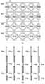
도 2는 도 1에 도시된 터치 센서(10)의 일 실시 형태의 일부의 평면도이고, 도 3은 도 2에 도시된 터치 센서를 층별로 분리한 평면도들이고, 도 4는 도 2에 도시된 복수의 수신 전극의 전기적 연결을 설명하기 위한 도면이다.FIG. 2 is a plan view of a part of an embodiment of the
도 2 내지 도 4를 참조하면, 본 발명의 일 실시 형태에 따른 터치 센서는 터치 입력 장치의 터치가 입력되는 영역에 배치될 수 있고, 터치 입력 장치에 포함된 디스플레이 패널의 표시 영역에 배치될 수 있다.Referring to FIGS. 2 to 4 , the touch sensor according to an embodiment of the present invention may be disposed in an area where a touch is input of the touch input device and may be disposed in a display area of a display panel included in the touch input device. there is.
본 발명의 일 실시 형태에 따른 터치 센서는 복수의 구동 전극(TX0, TX1, TX2, TX3??)과 복수의 수신 전극(RX0, RX1, RX2, RX3, RX4,??)을 포함한다.A touch sensor according to an embodiment of the present invention includes a plurality of driving electrodes TX0, TX1, TX2, TX3?? and a plurality of receiving electrodes RX0, RX1, RX2, RX3, RX4,??.
복수의 구동 전극(TX0, TX1, TX2, TX3??)은 제0 구동 전극(TX0), 제1 구동 전극(TX1), 제2 구동 전극(TX2) 및 제3 구동 전극(TX3)를 포함할 수 있다.The plurality of driving electrodes TX0, TX1, TX2, TX3?? may include a zeroth driving electrode TX0, a first driving electrode TX1, a second driving electrode TX2, and a third driving electrode TX3. can
복수의 수신 전극(RX0, RX1, RX2, RX3, RX4,??)은 제0 수신 전극(RX0), 제1 수신 전극(RX1), 제2 수신 전극(RX2), 제3 수신 전극(RX3) 및 제4 수신 전극(RX4)를 포함할 수 있다.The plurality of receiving electrodes RX0 , RX1 , RX2 , RX3 , RX4 ?? include a 0th receiving electrode RX0 , a first receiving electrode RX1 , a second receiving electrode RX2 , and a third receiving electrode RX3 . and a fourth receiving electrode RX4.
복수의 구동 전극(TX0, TX1, TX2, TX3??)은 제2 방향(또는 세로 방향)을 따라 배열되고, 복수의 수신 전극(RX0, RX1, RX2, RX3, RX4,??)은 상기 제2 방향과 수직한 제1 방향(또는 가로 방향)을 따라 배열될 수 있다. 여기서, 복수의 구동 전극(TX0, TX1, TX2, TX3??)은 상기 제1 방향(또는 가로 방향)을 따라 배열되고, 복수의 수신 전극(RX0, RX1, RX2, RX3, RX4,??)은 상기 제2 방향(또는 세로 방향)을 따라 배열될 수도 있다.A plurality of driving electrodes TX0, TX1, TX2, TX3?? are arranged along the second direction (or vertical direction), and a plurality of receiving electrodes RX0, RX1, RX2, RX3, RX4,?? It may be arranged along a first direction (or transverse direction) perpendicular to the two directions. Here, the plurality of driving electrodes TX0, TX1, TX2, TX3?? are arranged along the first direction (or horizontal direction), and the plurality of receiving electrodes RX0, RX1, RX2, RX3, RX4,?? may be arranged along the second direction (or vertical direction).
복수의 구동 전극(TX0, TX1, TX2, TX3??)과 복수의 수신 전극(RX0, RX1, RX2, RX3, RX4,??)의 사이에는 소정의 커패시턴스가 형성될 수 있다. 이러한 커패시턴스는 해당 지점 또는 그 주변에서 터치 입력이 발생할 시 변화된다. 따라서, 복수의 수신 전극(RX0, RX1, RX2, RX3, RX4,??)으로부터 출력되는 신호로부터 커패시턴스의 변화량을 검출함으로써 터치 여부 및 터치 입력을 검출할 수 있다.A predetermined capacitance may be formed between the plurality of driving electrodes TX0 , TX1 , TX2 , TX3 ?? and the plurality of receiving electrodes RX0 , RX1 , RX2 , RX3 , RX4 ?? This capacitance changes when a touch input occurs at or around the corresponding point. Accordingly, it is possible to detect touch and touch input by detecting capacitance variation from signals output from the plurality of receiving electrodes RX0 , RX1 , RX2 , RX3 , RX4 , ??.
복수의 구동 전극(TX0, TX1, TX2, TX3??) 각각은, 도 3의 (a)에 도시된 바와 같이, 제1 방향으로 연장된 직사각형 패턴 또는 바(bar) 패턴의 형상을 가지며, 내부에 제1 방향을 따라 배열된 복수의 개구부(O)을 가질 수 있다.Each of the plurality of driving electrodes TX0, TX1, TX2, and TX3?? has a shape of a rectangular pattern or a bar pattern extending in the first direction, as shown in (a) of FIG. It may have a plurality of openings (O) arranged along the first direction.
각 개구부(O) 내에는 하나의 수신 전극이 배치된다. 각 개구부(O)의 형상은 내부에 배치된 하나의 수신 전극의 형상과 대응된다. 예를 들어, 도 3에 도시된 바와 같이, 복수의 개구부(O) 중 좌우측 가장자리에 배치된 개구부들을 제외한 나머지들은 마름모꼴의 형상을 가질 수 있고, 상기 좌우측 가장자리에 배치된 개구부들은 삼각형의 형상을 가질 수 있다. 도면으로 도시하지 않았지만, 모든 개구부(O)들이 마름모꼴의 형상을 가질 수도 있다. 복수의 개구부(O)의 다각형, 장방형, 원형 또는 타원형 등의 다양한 형상을 가질 수 있다.One receiving electrode is disposed in each opening O. The shape of each opening O corresponds to the shape of one receiving electrode disposed therein. For example, as shown in FIG. 3 , among the plurality of openings O, except for the openings disposed on the left and right edges, the rest may have a lozenge shape, and the openings disposed on the left and right edges may have a triangular shape. can Although not shown in the drawings, all of the openings O may have a lozenge shape. The plurality of openings O may have various shapes such as a polygon, a rectangle, a circle, or an ellipse.
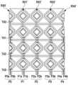
각 수신 전극(RX0, RX1, RX2, RX3, RX4,??)은, 복수의 수신 전극 패턴(RX0a, RX0b, RX1a, RX1b, RX2a, RX2b, RX3a, RX3b, RX4a, RX4b)과 연결 패턴(P0, P1, P2, P3, P4)을 포함한다.Each receiving electrode (RX0, RX1, RX2, RX3, RX4,??) is connected to a plurality of receiving electrode patterns (RX0a, RX0b, RX1a, RX1b, RX2a, RX2b, RX3a, RX3b, RX4a, RX4b) and a connection pattern (P0). , P1, P2, P3, P4).
도 3의 (a)에 도시된 바와 같이, 복수의 구동 전극(TX0, TX1, TX2, TX3??)과 복수의 수신 전극 패턴(RX0a, RX0b, RX1a, RX1b, RX2a, RX2b, RX3a, RX3b, RX4a, RX4b)은 제1 층(first layer)에 배치될 수 있다. 여기서, 제1 층(first layer)에 배치된 복수의 구동 전극(TX0, TX1, TX2, TX3??)과 복수의 수신 전극 패턴(RX0a, RX0b, RX1a, RX1b, RX2a, RX2b, RX3a, RX3b, RX4a, RX4b)은 메탈 메쉬로 구현될 수 있다. 도 3의 (b)에 도시된 바와 같이, 복수의 연결 패턴들(P0a, P0b, P1a, P1b, P2a, P2b, P3a, P3b, P4a, P4b)은 제2 층(second layer)에 배치될 수 있다. 제2 층은 도 3의 (a)의 제1 층과 다른 층이며, 제1 층으로부터 전기적으로 절연된다. 여기서, 복수의 연결 패턴들(P0a, P0b, P1a, P1b, P2a, P2b, P3a, P3b, P4a, P4b)은 메탈 메쉬로 구현될 수 있다. 도 3의 (a)의 제1 층은 도 3의 (b)의 제2 층 상에 배치될 수도 있고, 그 반대도 가능하다.As shown in (a) of FIG. 3, a plurality of driving electrodes TX0, TX1, TX2, TX3?? and a plurality of receiving electrode patterns RX0a, RX0b, RX1a, RX1b, RX2a, RX2b, RX3a, RX3b, RX4a and RX4b) may be disposed on a first layer. Here, a plurality of driving electrodes (TX0, TX1, TX2, TX3??) and a plurality of receiving electrode patterns (RX0a, RX0b, RX1a, RX1b, RX2a, RX2b, RX3a, RX3b, RX4a, RX4b) may be implemented as a metal mesh. As shown in (b) of FIG. 3 , the plurality of connection patterns P0a, P0b, P1a, P1b, P2a, P2b, P3a, P3b, P4a, and P4b may be disposed on a second layer. there is. The second layer is a layer different from the first layer in Fig. 3(a) and is electrically insulated from the first layer. Here, the plurality of connection patterns P0a, P0b, P1a, P1b, P2a, P2b, P3a, P3b, P4a, and P4b may be implemented as a metal mesh. The first layer of FIG. 3(a) may be disposed on the second layer of FIG. 3(b), and vice versa.
각 수신 전극에 포함된 복수의 수신 전극 패턴은 적어도 둘 이상의 그룹으로 나뉠 수 있다. 하나의 그룹의 수신 전극 패턴들 사이사이에 다른 하나의 그룹 내의 수신 전극 패턴들이 하나씩 교번하며 배치된다. 하나의 그룹의 수신 전극 패턴들은 다른 하나의 그룹 내의 수신 전극 패턴들과 전기적으로 분리된다. 각 수신 전극에 포함된 복수의 연결 패턴은 하나의 그룹 내의 수신 전극 패턴들을 전기적으로 연결하는 제1 연결 패턴들과 다른 하나의 그룹 내의 수신 전극들을 전기적으로 연결하는 제2 연결 패턴들을 포함한다.A plurality of receiving electrode patterns included in each receiving electrode may be divided into at least two groups. Receiving electrode patterns in another group are alternately disposed between the receiving electrode patterns of one group. Receiving electrode patterns in one group are electrically separated from receiving electrode patterns in another group. The plurality of connection patterns included in each receiving electrode include first connection patterns electrically connecting the receiving electrode patterns in one group and second connection patterns electrically connecting the receiving electrodes in another group.
예를 들어, 제0 수신 전극(RX0)은 복수의 수신 전극 패턴(RX0a, RX0b)과 복수의 연결 패턴(P0)을 포함할 수 있다. 복수의 수신 전극 패턴(RX0a, RX0b)은 제2 방향을 따라 하나씩 교번하며 배열된 제1 그룹의 수신 전극 패턴(RX0a)들과 제2 그룹의 수신 전극 패턴(RX0b)들을 포함할 수 있다. 제1 그룹의 수신 전극 패턴(RX0a)들과 제2 그룹의 수신 전극 패턴(RX0b)들은 서로 전기적으로 분리될 수 있다. 제0 연결 패턴(P0)은 제1 그룹의 수신 전극 패턴(RX0a)들을 전기적으로 연결하는 제1 연결 패턴(P0a)들과 제2 그룹의 수신 전극 패턴(RX0b)들을 전기적으로 연결하는 제2 연결 패턴(P0b)들을 포함할 수 있다.For example, the zeroth receiving electrode RX0 may include a plurality of receiving electrode patterns RX0a and RX0b and a plurality of connection patterns P0. The plurality of receiving electrode patterns RX0a and RX0b may include a first group of receiving electrode patterns RX0a and a second group of receiving electrode patterns RX0b that are alternately arranged one by one along the second direction. The receiving electrode patterns RX0a of the first group and the receiving electrode patterns RX0b of the second group may be electrically separated from each other. The 0th connection pattern P0 is a second connection electrically connecting the first connection patterns P0a electrically connecting the first group of receiving electrode patterns RX0a and the second group receiving electrode patterns RX0b. Patterns P0b may be included.
제1 수신 전극(RX1)은 복수의 수신 전극 패턴(RX1a, RX1b)과 복수의 연결 패턴(P1)을 포함할 수 있다. 복수의 수신 전극 패턴(RX1a, RX1b)은 제2 방향을 따라 하나씩 교번하며 배열된 제1 그룹의 수신 전극 패턴(RX1a)들과 제2 그룹의 수신 전극 패턴(RX1b)들을 포함할 수 있다. 제1 그룹의 수신 전극 패턴(RX1a)들과 제2 그룹의 수신 전극 패턴(RX1b)들은 서로 전기적으로 분리될 수 있다. 제1 연결 패턴(P1)은 제1 그룹의 수신 전극 패턴(RX1a)들을 전기적으로 연결하는 제1 연결 패턴(P1a)들과 제2 그룹의 수신 전극 패턴(RX1b)들을 전기적으로 연결하는 제2 연결 패턴(P1b)들을 포함할 수 있다.The first receiving electrode RX1 may include a plurality of receiving electrode patterns RX1a and RX1b and a plurality of connection patterns P1. The plurality of receiving electrode patterns RX1a and RX1b may include a first group of receiving electrode patterns RX1a and a second group of receiving electrode patterns RX1b that are alternately arranged one by one along the second direction. The receiving electrode patterns RX1a of the first group and the receiving electrode patterns RX1b of the second group may be electrically separated from each other. The first connection pattern P1 is a second connection electrically connecting the first connection patterns P1a electrically connecting the receiving electrode patterns RX1a of the first group and the receiving electrode patterns RX1b of the second group. Patterns P1b may be included.
제2 수신 전극(RX2)은 복수의 수신 전극 패턴(RX2a, RX2b)과 복수의 연결 패턴(P2)을 포함할 수 있다. 복수의 수신 전극 패턴(RX2a, RX2b)은 제2 방향을 따라 하나씩 교번하며 배열된 제1 그룹의 수신 전극 패턴(RX2a)들과 제2 그룹의 수신 전극 패턴(RX2b)들을 포함할 수 있다. 제1 그룹의 수신 전극 패턴(RX2a)들과 제2 그룹의 수신 전극 패턴(RX2b)들은 서로 전기적으로 분리될 수 있다. 제2 연결 패턴(P2)은 제1 그룹의 수신 전극 패턴(RX2a)들을 전기적으로 연결하는 제1 연결 패턴(P2a)들과 제2 그룹의 수신 전극 패턴(RX2b)들을 전기적으로 연결하는 제2 연결 패턴(P2b)들을 포함할 수 있다.The second receiving electrode RX2 may include a plurality of receiving electrode patterns RX2a and RX2b and a plurality of connection patterns P2. The plurality of receiving electrode patterns RX2a and RX2b may include a first group of receiving electrode patterns RX2a and a second group of receiving electrode patterns RX2b that are alternately arranged one by one along the second direction. The receiving electrode patterns RX2a of the first group and the receiving electrode patterns RX2b of the second group may be electrically separated from each other. The second connection pattern P2 is a second connection electrically connecting the first connection patterns P2a electrically connecting the first group of receiving electrode patterns RX2a and the second group of receiving electrode patterns RX2b. Patterns P2b may be included.
제3 수신 전극(RX3)은 복수의 수신 전극 패턴(RX3a, RX3b)과 복수의 연결 패턴(P3)을 포함할 수 있다. 복수의 수신 전극 패턴(RX3a, RX3b)은 제2 방향을 따라 하나씩 교번하며 배열된 제1 그룹의 수신 전극 패턴(RX3a)들과 제2 그룹의 수신 전극 패턴(RX3b)들을 포함할 수 있다. 제1 그룹의 수신 전극 패턴(RX3a)들과 제2 그룹의 수신 전극 패턴(RX3b)들은 서로 전기적으로 분리될 수 있다. 제3 연결 패턴(P3)은 제1 그룹의 수신 전극 패턴(RX3a)들을 전기적으로 연결하는 제1 연결 패턴(P3a)들과 제2 그룹의 수신 전극 패턴(RX3b)들을 전기적으로 연결하는 제2 연결 패턴(P3b)들을 포함할 수 있다.The third receiving electrode RX3 may include a plurality of receiving electrode patterns RX3a and RX3b and a plurality of connection patterns P3. The plurality of receiving electrode patterns RX3a and RX3b may include a first group of receiving electrode patterns RX3a and a second group of receiving electrode patterns RX3b that are alternately arranged one by one along the second direction. The receiving electrode patterns RX3a of the first group and the receiving electrode patterns RX3b of the second group may be electrically separated from each other. The third connection pattern P3 is a second connection electrically connecting the first connection patterns P3a electrically connecting the first group of receiving electrode patterns RX3a and the second group receiving electrode patterns RX3b. Patterns P3b may be included.
제4 수신 전극(RX4)은 복수의 수신 전극 패턴(RX4a, RX4b)과 복수의 연결 패턴(P4)을 포함할 수 있다. 복수의 수신 전극 패턴(RX4a, RX4b)은 제2 방향을 따라 하나씩 교번하며 배열된 제1 그룹의 수신 전극 패턴(RX4a)들과 제2 그룹의 수신 전극 패턴(RX4b)들을 포함할 수 있다. 제1 그룹의 수신 전극 패턴(RX4a)들과 제2 그룹의 수신 전극 패턴(RX4b)들은 서로 전기적으로 분리될 수 있다. 제4 연결 패턴(P4)은 제1 그룹의 수신 전극 패턴(RX4a)들을 전기적으로 연결하는 제1 연결 패턴(P4a)들과 제2 그룹의 수신 전극 패턴(RX4b)들을 전기적으로 연결하는 제2 연결 패턴(P4b)들을 포함할 수 있다.The fourth receiving electrode RX4 may include a plurality of receiving electrode patterns RX4a and RX4b and a plurality of connection patterns P4. The plurality of receiving electrode patterns RX4a and RX4b may include a first group of receiving electrode patterns RX4a and a second group of receiving electrode patterns RX4b that are alternately arranged one by one along the second direction. The receiving electrode patterns RX4a of the first group and the receiving electrode patterns RX4b of the second group may be electrically separated from each other. The fourth connection pattern P4 is a second connection electrically connecting the first connection patterns P4a electrically connecting the receiving electrode patterns RX4a of the first group and the receiving electrode patterns RX4b of the second group. Patterns P4b may be included.
복수의 수신 전극 패턴(RX0a, RX0b, RX1a, RX1b, RX2a, RX2b, RX3a, RX3b, RX4a, RX4b)은, 복수의 구동 전극(TX0, TX1, TX2, TX3??)의 복수의 개구부(O) 내부에 배치된다. 하나의 수신 전극 패턴은 하나의 개구부(O) 내부에 배치된다. 각 수신 전극 패턴의 형상은 그와 대응되는 개구부의 형상에 대응된다.The plurality of receiving electrode patterns RX0a, RX0b, RX1a, RX1b, RX2a, RX2b, RX3a, RX3b, RX4a, and RX4b include a plurality of openings O of the plurality of driving electrodes TX0, TX1, TX2, and TX3?? placed inside One receiving electrode pattern is disposed inside one opening O. The shape of each receiving electrode pattern corresponds to the shape of the corresponding opening.
임의의 수신 전극(RX1)에 있어서, 서로 인접하여 배치된 제1 그룹 내의 수신 전극 패턴(RX1a)과 제2 그룹 내의 수신 전극 패턴(RX1b) 사이에는, 제1 그룹 내의 수신 전극 패턴(RX1a) 주변에 바로 인접한 구동 전극(TX0)의 일부와 제2 그룹 내의 수신 전극 패턴(RX1b) 주변에 바로 인접한 구동 전극(TX1)의 일부가 함께 배치된다.In the arbitrary receiving electrodes RX1, between the receiving electrode patterns RX1a in the first group and the receiving electrode patterns RX1b in the second group disposed adjacent to each other, the periphery of the receiving electrode patterns RX1a in the first group A part of the driving electrode TX0 immediately adjacent to and a part of the driving electrode TX1 immediately adjacent to the periphery of the receiving electrode pattern RX1b in the second group are disposed together.
임의의 구동 전극(TX0)은 하나의 그룹의 수신 전극 패턴(RX0a, RX1a, RX2a, RX3a, RX4a) 주변에 바로 인접하여 배치되고, 다른 그룹의 수신 전극 패턴(RX0b, RX1b, RX2b, RX3b, RX4b) 주변에 바로 인접하여 배치된 다른 구동 전극(TX1)은 상기 임의의 구동 전극(TX0)에 의해, 상기 하나의 그룹의 수신 전극 패턴(RX0a, RX1a, RX2a, RX3a, RX4a)과 분리되도록 배치된다.An arbitrary driving electrode TX0 is disposed immediately adjacent to one group of receiving electrode patterns RX0a, RX1a, RX2a, RX3a, and RX4a, and another group of receiving electrode patterns RX0b, RX1b, RX2b, RX3b, and RX4b. ) The other driving electrode TX1 disposed immediately adjacent to the periphery is disposed to be separated from the one group of receiving electrode patterns RX0a, RX1a, RX2a, RX3a, and RX4a by the arbitrary driving electrode TX0. .
연결 패턴들(P0a, P0b, P1a, P1b, P2a, P2b, P3a, P3b, P4a, P4b) 각각은 제2 방향을 따라 연장된 바(bar) 패턴의 형상을 가질 수 있으며, 적어도 하나 이상의 도전성 비아(v)를 포함한다. 도전성 비아(v)는 연결 패턴들 각각의 양 단부에 배치될 수 있다.Each of the connection patterns P0a, P0b, P1a, P1b, P2a, P2b, P3a, P3b, P4a, and P4b may have a bar pattern shape extending along the second direction, and include at least one conductive via. (v) includes. Conductive vias (v) may be disposed at both ends of each of the connection patterns.
제0 수신 전극(RX0)에 있어서, 제1 연결 패턴(P0a)들 각각은 제1 그룹의 수신 전극 패턴(RX0a)들 중 서로 인접한 두 개의 수신 전극 패턴(RX0a)을 도전성 비아(v)를 통해 전기적으로 연결하고, 상기 서로 인접한 두 개의 수신 전극 패턴(RX0a) 사이에 배치된 제2 그룹의 수신 전극 패턴(RX0b) 아래에 오버랩되도록 배치된다. 제2 연결 패턴(P0b)들 각각은 제2 그룹의 수신 전극 패턴(RX0b)들 중 서로 인접한 두 개의 수신 전극 패턴(RX0b)을 도전성 비아(v)를 통해 전기적으로 연결하고, 상기 서로 인접한 두 개의 수신 전극 패턴(RX0b) 사이에 배치된 제1 그룹의 수신 전극 패턴(RX0a) 아래에 오버랩되도록 배치된다. 나머지 수신 전극(RX1, RX2, RX3, RX4)의 제1 연결 패턴들(P1a, P2a, P3a, P4a)과 제2 연결 패턴들(P1b, P2b, P3b, P4b)도 앞서 설명한 같이 동일한 방식으로 배치된다.In the 0th receiving electrode RX0, each of the first connection patterns P0a connects two adjacent receiving electrode patterns RX0a among the first group of receiving electrode patterns RX0a through the conductive via v. electrically connected to each other, and disposed overlapping under the second group of receiving electrode patterns RX0b disposed between the two adjacent receiving electrode patterns RX0a. Each of the second connection patterns P0b electrically connects two adjacent receiving electrode patterns RX0b of the second group of receiving electrode patterns RX0b through a conductive via v, and It is disposed to overlap under the first group of receiving electrode patterns RX0a disposed between the receiving electrode patterns RX0b. The first connection patterns P1a, P2a, P3a, and P4a and the second connection patterns P1b, P2b, P3b, and P4b of the remaining receiving electrodes RX1, RX2, RX3, and RX4 are also disposed in the same manner as described above. do.
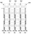
이하에서는 복수의 구동 전극(TX0, TX1, TX2, TX3)으로 구동 신호가 인가될 경우의 동작을 상세히 설명한다. 설명의 편의상, 제1 수신 전극(RX1)의 동작과 도 1의 감지부(11)의 동작을 구체적으로 설명한다.Hereinafter, an operation when a driving signal is applied to the plurality of driving electrodes TX0 , TX1 , TX2 , and TX3 will be described in detail. For convenience of explanation, the operation of the first receiving electrode RX1 and the operation of the
복수의 구동 전극(TX0, TX1, TX2, TX3)으로 구동 신호가 인가되면, 제1 연결 패턴(P1)을 통해 두 개의 감지 신호가 출력된다. 제1 신호는 제1 연결 패턴(P1a)을 통해 출력되는 신호이고, 제2 신호는 제2 연결 패턴(P1b)을 통해 출력되는 신호이다. 따라서, 각 수신 전극(RX0, RX1, RX2, RX3, RX4)마다 2 채널의 제1 및 제2 신호가 출력된다. 상기 제1 및 제2 신호는 동시에 출력되며, 출력되는 제1 및 제2 신호는 도 2의 감지부(11)로 출력될 수 있다.When a driving signal is applied to the plurality of driving electrodes TX0 , TX1 , TX2 , and TX3 , two detection signals are output through the first connection pattern P1 . The first signal is a signal output through the first connection pattern P1a, and the second signal is a signal output through the second connection pattern P1b. Accordingly, first and second signals of two channels are output to each of the receiving electrodes RX0 , RX1 , RX2 , RX3 , and RX4 . The first and second signals are simultaneously output, and the output first and second signals may be output to the
구동 신호가 인가되는 구동 전극(TX0, TX1, TX2, TX3??)에 따라, 제1 신호와 제2 신호 중 어느 하나는 액티브 채널 신호(또는 액티브 수신 신호(ARX))가 될 수 있고, 나머지 다른 하나는 더미 채널 신호(또는 더미 수신 신호(DRX))가 될 수 있다. 구체적으로, 제1 그룹의 수신 전극 패턴(RX1a)이 배치된 구동 전극(TX0, TX2)에 구동 신호가 인가되면, 제1 연결 패턴(P1a)을 통해 출력되는 제1 신호가 액티브 채널 신호가 되고, 제2 연결 패턴(P1b)을 통해 출력되는 제2 신호가 더미 채널 신호가 된다. 반면, 제2 그룹의 수신 전극 패턴(RX1b)이 배치된 구동 전극(TX1, TX3)에 구동 신호가 인가되면, 제2 연결 패턴(P1b)을 통해 출력되는 제2 신호가 액티브 채널 신호가 되고, 제1 연결 패턴(P1a)을 통해 출력되는 제1 신호가 더미 채널 신호가 된다.Depending on the driving electrodes TX0, TX1, TX2, TX3 ?? to which the driving signal is applied, one of the first signal and the second signal may be an active channel signal (or active reception signal ARX), and the other The other may be a dummy channel signal (or dummy received signal DRX). Specifically, when a driving signal is applied to the driving electrodes TX0 and TX2 on which the first group of receiving electrode patterns RX1a are disposed, the first signal output through the first connection pattern P1a becomes an active channel signal, , the second signal output through the second connection pattern P1b becomes a dummy channel signal. On the other hand, when a driving signal is applied to the driving electrodes TX1 and TX3 on which the receiving electrode pattern RX1b of the second group is disposed, the second signal output through the second connection pattern P1b becomes an active channel signal, The first signal output through the first connection pattern P1a becomes a dummy channel signal.
예를 들어, 도 2에 도시된 바와 같이, 제1 구동 전극(TX1)에 구동 신호가 인가되고, 객체(점선)가 제1 구동 전극(TX1)과 제1 수신 전극(RX1)의 교차 지점에 근접 또는 접촉된 것을 가정하면, 제1 수신 전극(RX1)의 제2 그룹에 속한 수신 전극 패턴(RX1b)과 제1 구동 전극(TX1) 사이에 형성된 커패시턴스(또는, 액티브 커패시턴스)가 변화된다. 커패시턴스 변화량 정보를 포함한 제2 신호는 액티브 채널 신호로서, 제2 연결 패턴(P1b)을 통해 출력된다. 여기서, 상기 제2 신호에는 LGM 노이즈 신호와 디스플레이 패널에 의한 디스플레이 노이즈 신호를 포함할 수 있다.For example, as shown in FIG. 2 , a driving signal is applied to the first driving electrode TX1 and an object (dotted line) is located at the intersection of the first driving electrode TX1 and the first receiving electrode RX1. Assuming proximity or contact, the capacitance (or active capacitance) formed between the receiving electrode pattern RX1b belonging to the second group of the first receiving electrode RX1 and the first driving electrode TX1 is changed. The second signal including capacitance variation information is an active channel signal and is output through the second connection pattern P1b. Here, the second signal may include an LGM noise signal and a display noise signal by the display panel.
그리고, 제1 수신 전극(RX1)의 제1 그룹에 속한 수신 전극 패턴(RX1a) 사이에 형성된 커패시턴스(또는, 더미 커패시턴스)도 변화된다. 커패시턴스 변화량 정보를 포함한 제1 신호는 더미 채널 신호로서, 제1 연결 패턴(P1a)을 통해 출력된다. 여기서, 상기 제1 신호에는 LGM 노이즈 신호와 디스플레이 패널에 의한 디스플레이 노이즈 신호를 포함할 수 있다. 여기서, 객체(점선)와 접촉된 제2 그룹에 속한 수신 전극 패턴(RX1b)와 제1 그룹에 속한 수신 전극 패턴(RX1a)의 단면적이 동일하므로, 각각으로 거의 동일 또는 유사한 LGM 노이즈 신호가 입력될 수 있고, 디스플레이 패널에 의한 디스플레이 노이즈 신호도 거의 동일하게 입력될 수 있다.Also, the capacitance (or dummy capacitance) formed between the receiving electrode patterns RX1a belonging to the first group of the first receiving electrodes RX1 is changed. The first signal including capacitance variation information is a dummy channel signal and is output through the first connection pattern P1a. Here, the first signal may include an LGM noise signal and a display noise signal by a display panel. Here, since the cross-sectional area of the receiving electrode pattern RX1b belonging to the second group and the receiving electrode pattern RX1a belonging to the first group contacting the object (dotted line) are the same, almost the same or similar LGM noise signals are input. and the display noise signal by the display panel can be input in substantially the same way.
도 1에 도시된 감지부(11)는, 제2 연결 패턴(P1b)을 통해 출력되는 제2 신호에서, 제1 연결 패턴(P1a)을 통해 출력되는 제1 신호를 차감함으로서, 제2 그룹에 속한 수신 전극 패턴(RX1b)와 제1 그룹에 속한 수신 전극 패턴(RX1a)으로 입력된 LGM 노이즈 신호와 디스플레이 노이즈 신호를 상쇄시킬 수 있다. 상기 차감에 의해서 액티브 채널 신호인 제2 신호에 포함된 액티브 커패시턴스 변화량이 제1 신호에 포함된 더미 커패시턴스 변화량에 의해 다소 줄어들지만, 제1 구동 전극(TX1)과 수신 전극 패턴(RX1a) 사이의 거리가 제1 구동 전극(TX1)과 수신 전극 패턴(RX1b) 사이의 거리보다 상대적으로 더 멀기 때문에 제1 신호에 포함된 더미 커패시턴스 변화량이 제2 신호에 포함된 액티브 커패시턴스 변화량보다 상대적으로 작다. 따라서, 차감된 액티브 커패시턴스 변화량만으로도 터치 여부 또는/및 터치 위치를 검출하는데 충분하다.The
한편, 구동 신호가, 제1 구동 전극(TX1)이 아닌, 제0 구동 전극(TX0)에 인가되면, 도 1에 도시된 감지부(11)는, 반대로 연결 패턴(P1a)을 통해 출력되는 제1 신호(액티브 채널 신호)에서, 연결 패턴(P1b)을 통해 출력되는 제2 신호(더미 채널 신호)를 차감함으로서, 제1 그룹에 속한 수신 전극 패턴(RX1a)와 제2 그룹에 속한 수신 전극 패턴(RX1b)로 입력된 LGM 노이즈 신호와 디스플레이 노이즈 신호를 상쇄시킬 수 있다. 따라서, 터치 센싱 시에 발생할 수 있는 다양한 노이즈, 예를 들어, 디스플레이 노이즈 및 LGM 노이즈 등을 제거할 수 있는 이점이 있다.Meanwhile, when the driving signal is applied to the 0th driving electrode TX0 instead of the 1st driving electrode TX1 , the
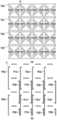
도 5는 도 1에 도시된 터치 센서(10)의 다른 실시 형태의 일부의 평면도이고, 도 6은 도 5에 도시된 터치 센서를 층별로 분리한 평면도들이고, 도 7은 도 5에 도시된 복수의 수신 전극의 전기적 연결을 설명하기 위한 도면이다.FIG. 5 is a plan view of a part of another embodiment of the
도 5 내지 도 7에 도시된 본 발명의 다른 실시 형태에 따른 터치 센서는, 도 2 내지 도 4에 도시된 본 발명의 일 실시 형태에 따른 터치 센서와 비교하여, 복수의 수신 전극(RX0', RX1', RX2', RX3', RX4')에서 차이가 있다. 특히, 각 수신 전극(RX0', RX1', RX2', RX3', RX4')에 포함된 복수의 수신 전극 패턴(RX1a')의 구조가 상이하다. 이하에서 복수의 수신 전극 패턴(RX1a')의 구조를 상세히 설명하고 나머지 구성들은 앞서 상술한 내용으로 대체하기로 한다.Compared with the touch sensor according to another embodiment of the present invention shown in FIGS. 5 to 7 , a plurality of receiving electrodes RX0′, There is a difference in RX1', RX2', RX3', RX4'). In particular, the structures of the plurality of receiving electrode patterns RX1a' included in the respective receiving electrodes RX0', RX1', RX2', RX3', and RX4' are different. Hereinafter, the structure of the plurality of receiving electrode patterns RX1a' will be described in detail, and the remaining components will be replaced with the above-described contents.
각 수신 전극(RX0', RX1', RX2', RX3', RX4')에 포함된 복수의 수신 전극 패턴(RX1a')은 내부에 개구부(O')을 갖고, 개구부(O') 내부에 배치된 더미 패턴(DX1a)을 포함한다. 여기서, 더미 패턴(DX1a)은 개구부(O')와 대응되는 형상을 가질 수 있다.The plurality of receiving electrode patterns RX1a' included in each of the receiving electrodes RX0', RX1', RX2', RX3', and RX4' have an opening O' therein and disposed inside the opening O'. A dummy pattern DX1a is included. Here, the dummy pattern DX1a may have a shape corresponding to the opening O'.
더미 패턴(DX1a)은 연결 패턴들(P0a, P0b, P1a, P1b, P2a, P2b, P3a, P3b, P4a, P4b)과 전기적으로 연결되지 않는다. 더미 패턴(DX1a)은 전기적으로 플로팅된 상태를 유지한다.The dummy pattern DX1a is not electrically connected to the connection patterns P0a, P0b, P1a, P1b, P2a, P2b, P3a, P3b, P4a, and P4b. The dummy pattern DX1a remains electrically floating.
도 5 내지 도 7에 도시된 본 발명의 다른 실시 형태에 따른 터치 센서의 동작은 도 2 내지 도 4에 도시된 본 발명의 일 실시 형태에 따른 터치 센서의 동작과 동일하다. 따라서, 도 5 내지 도 7에 도시된 본 발명의 다른 실시 형태에 따른 터치 센서를 포함하는 터치 입력 장치도 터치 센싱 시에 발생할 수 있는 다양한 노이즈, 예를 들어, 디스플레이 노이즈 및 LGM 노이즈 등을 제거할 수 있는 이점이 있다.The operation of the touch sensor according to another embodiment of the present invention shown in FIGS. 5 to 7 is the same as the operation of the touch sensor according to one embodiment of the present invention shown in FIGS. 2 to 4 . Therefore, the touch input device including the touch sensor according to another embodiment of the present invention shown in FIGS. 5 to 7 can also remove various noises that may occur during touch sensing, such as display noise and LGM noise. There are advantages that can be
도 8은 도 1에 도시된 터치 센서(10)의 또 다른 실시 형태의 일부의 평면도이고, 도 9는 도 8에 도시된 터치 센서를 층별로 분리한 평면도들이다.FIG. 8 is a plan view of a part of another embodiment of the
도 8 내지 도 9에 도시된 본 발명의 또 다른 실시 형태에 따른 터치 센서는, 도 2 내지 도 4에 도시된 본 발명의 일 실시 형태에 따른 터치 센서와 비교하여, 복수의 수신 전극(RX0'', RX1'', RX2'', RX3'', RX4'')에서 차이가 있다. 특히, 각 수신 전극(RX0'', RX1'', RX2'', RX3'', RX4'')에 포함된 복수의 연결 패턴(P0', P1', P2', P3, P4')의 배치 형태가 상이하다. 이하에서 각 연결 패턴(P0', P1', P2', P3, P4')의 배치 형태를 상세히 설명하고 나머지 구성들은 앞서 상술한 내용으로 대체하기로 한다.Compared to the touch sensor according to another embodiment of the present invention shown in FIGS. 8 to 9, the plurality of receiving electrodes RX0' are compared to the touch sensor according to the embodiment shown in FIGS. 2 to 4 ', RX1'', RX2'', RX3'', RX4''). In particular, the arrangement of the plurality of connection patterns P0', P1', P2', P3, and P4' included in the respective receiving electrodes RX0'', RX1'', RX2'', RX3'', and RX4'' The shape is different. Hereinafter, the arrangement of each connection pattern P0', P1', P2', P3, and P4' will be described in detail, and the remaining configurations will be replaced with the above-described contents.
각 연결 패턴(P0', P1', P2', P3, P4')은 제1 연결 패턴들(P0a', P1a', P2a', P3a', P4a')과 제2 연결 패턴들(P0b', P1b', P2b', P3b', P4b')을 포함한다.Each of the connection patterns P0', P1', P2', P3, and P4' includes the first connection patterns P0a', P1a', P2a', P3a', and P4a' and the second connection patterns P0b', P1b', P2b', P3b', P4b').
각 제1 연결 패턴들(P0a', P1a', P2a', P3a', P4a')은 제1 그룹의 2개의 수신 전극 패턴(RX0a, RX1a, RX2a, RX3a, RX4a)을 전기적으로 연결하되, 상기 2개의 수신 전극 패턴 사이에 배치된 제2 그룹의 수신 전극 패턴(RX0b, RX1b, RX2b, RX3b, RX4b)과 겹치지 않도록 배치된다. 예를 들어, 각 제1 연결 패턴들(P0a', P1a', P2a', P3a', P4a')의 적어도 일 부분은 상기 제2 그룹의 수신 전극 패턴(RX0b, RX1b, RX2b, RX3b, RX4b)과 겹치지 않도록, 상기 제2 그룹의 수신 전극 패턴(RX0b, RX1b, RX2b, RX3b, RX4b)과 상기 제2 그룹의 수신 전극 패턴(RX0b, RX1b, RX2b, RX3b, RX4b)에 바로 인접하여 배치된 구동 전극(TX0, TX1, TX2, TX3) 사이에 배치될 수 있다. 한편, 나머지 부분은 상기 구동 전극(TX0, TX1, TX2, TX3)과 겹치도록 배치될 수 있다.Each of the first connection patterns P0a', P1a', P2a', P3a', and P4a' electrically connects the two receiving electrode patterns RX0a, RX1a, RX2a, RX3a, and RX4a of the first group. It is disposed so as not to overlap with the second group of receiving electrode patterns (RX0b, RX1b, RX2b, RX3b, RX4b) disposed between the two receiving electrode patterns. For example, at least a portion of each of the first connection patterns P0a', P1a', P2a', P3a', and P4a' is the receiving electrode pattern RX0b, RX1b, RX2b, RX3b, and RX4b of the second group. Driving disposed directly adjacent to the receiving electrode patterns RX0b, RX1b, RX2b, RX3b, and RX4b of the second group and the receiving electrode patterns RX0b, RX1b, RX2b, RX3b, and RX4b of the second group so as not to overlap with It may be disposed between the electrodes TX0, TX1, TX2, and TX3. Meanwhile, the remaining portions may be disposed to overlap the driving electrodes TX0 , TX1 , TX2 , and TX3 .
각 제2 연결 패턴들(P0b', P1b', P2b', P3b', P4b')은 제2 그룹의 2개의 수신 전극 패턴(RX0b, RX1b, RX2b, RX3b, RX4b)을 전기적으로 연결하되, 상기 2개의 수신 전극 패턴 사이에 배치된 제1 그룹의 수신 전극 패턴(RX0a, RX1a, RX2a, RX3a, RX4a)과 겹치지 않도록 배치된다. 예를 들어, 각 제2 연결 패턴들(P0b', P1b', P2b', P3b', P4b')의 적어도 일 부분은 상기 제1 그룹의 수신 전극 패턴(RX0a, RX1a, RX2a, RX3a, RX4a)과 겹치지 않도록, 상기 제1 그룹의 수신 전극 패턴(RX0a, RX1a, RX2a, RX3a, RX4a)과 상기 제1 그룹의 수신 전극 패턴(RX0a, RX1a, RX2a, RX3a, RX4a)에 바로 인접하여 배치된 구동 전극(TX0, TX1, TX2, TX3) 사이에 배치될 수 있다. 한편, 나머지 부분은 상기 구동 전극(TX0, TX1, TX2, TX3)과 겹치도록 배치될 수 있다.Each of the second connection patterns P0b', P1b', P2b', P3b', and P4b' electrically connects the two receiving electrode patterns RX0b, RX1b, RX2b, RX3b, and RX4b of the second group. It is disposed not to overlap with the first group of receiving electrode patterns (RX0a, RX1a, RX2a, RX3a, RX4a) disposed between the two receiving electrode patterns. For example, at least a portion of each of the second connection patterns P0b', P1b', P2b', P3b', and P4b' is the receiving electrode pattern RX0a, RX1a, RX2a, RX3a, and RX4a of the first group. Driving disposed directly adjacent to the first group of receiving electrode patterns (RX0a, RX1a, RX2a, RX3a, and RX4a) and the first group of receiving electrode patterns (RX0a, RX1a, RX2a, RX3a, and RX4a) so as not to overlap with It may be disposed between the electrodes TX0, TX1, TX2, and TX3. Meanwhile, the remaining portions may be disposed to overlap the driving electrodes TX0 , TX1 , TX2 , and TX3 .
이러한 본 발명의 또 다른 실시 형태에 따른 터치 센서는, 도 2 내지 도 4에 도시된 본 발명의 일 실시 형태에 따른 터치 센서와 비교하여, 제1 연결 패턴과 제2 그룹의 수신 전극 패턴 사이 또는 제2 연결 패턴과 제1 그룹의 수신 전극 패턴 사이의 커패시턴스 값을 줄일 수 있는 이점이 있다.Compared to the touch sensor according to the embodiment of the present invention shown in FIGS. 2 to 4, the touch sensor according to another embodiment of the present invention is between the first connection pattern and the second group of receiving electrode patterns or There is an advantage in that a capacitance value between the second connection pattern and the receiving electrode pattern of the first group can be reduced.
한편, 별도의 도면으로 도시하지 않았지만, 도 5 내지 도 6에 도시된 더미 패턴(DX1a)이 본 발명의 또 다른 실시 형태에 따른 터치 센서에도 적용될 수 있다.Meanwhile, although not shown as a separate drawing, the dummy pattern DX1a shown in FIGS. 5 and 6 may be applied to a touch sensor according to another embodiment of the present invention.
도 10은 도 1에 도시된 터치 센서(10)의 또 다른 실시 형태의 일부의 평면도이고, 도 11은 도 10에 도시된 터치 센서를 층별로 분리한 평면도들이다.FIG. 10 is a plan view of a part of another embodiment of the
도 10 내지 도 11에 도시된 본 발명의 또 다른 실시 형태에 따른 터치 센서는, 도 2 내지 도 4에 도시된 본 발명의 일 실시 형태에 따른 터치 센서와 비교하여, 복수의 수신 전극(RX0''', RX1''', RX2''', RX3''')에서 차이가 있다. 특히, 각 수신 전극(RX0''', RX1''', RX2''', RX3''')에 포함된 복수의 수신 전극 패턴(RX0a-1, RX0a-2, RX0b-1, RX0b-2, RX1a-1, RX1a-2, RX1b-1, RX1b-2, RX2a-1, RX2a-2, RX2b-1, RX2b-2, RX3a-1, RX3a-2, RX3b-1, RX3b-2)과 복수의 연결 패턴(P0'', P1'', P2'', P3'')의 구조 및 배치 형태가 상이하다. 이하에서 수신 전극 패턴(RX0a-1, RX0a-2, RX0b-1, RX0b-2, RX1a-1, RX1a-2, RX1b-1, RX1b-2, RX2a-1, RX2a-2, RX2b-1, RX2b-2, RX3a-1, RX3a-2, RX3b-1, RX3b-2)과 연결 패턴(P0'', P1'', P2'', P3'')의 구조 및 배치 형태를 상세히 설명하고 나머지 구성들은 앞서 상술한 내용으로 대체하기로 한다.Compared to the touch sensor according to another embodiment of the present invention shown in FIGS. 10 to 11, a plurality of receiving electrodes RX0′ are compared to the touch sensor according to another embodiment of the present invention shown in FIGS. 2 to 4 . '', RX1''', RX2''', RX3'''). In particular, a plurality of receiving electrode patterns (RX0a-1, RX0a-2, RX0b-1, RX0b-2) included in each receiving electrode (RX0''', RX1''', RX2''', RX3''') , RX1a-1, RX1a-2, RX1b-1, RX1b-2, RX2a-1, RX2a-2, RX2b-1, RX2b-2, RX3a-1, RX3a-2, RX3b-1, RX3b-2) and The structures and arrangements of the plurality of connection patterns P0'', P1'', P2'', and P3'' are different. Below, the receiving electrode patterns (RX0a-1, RX0a-2, RX0b-1, RX0b-2, RX1a-1, RX1a-2, RX1b-1, RX1b-2, RX2a-1, RX2a-2, RX2b-1, The structure and arrangement of RX2b-2, RX3a-1, RX3a-2, RX3b-1, RX3b-2 and connection patterns (P0'', P1'', P2'', P3'') are described in detail, and the rest Configurations will be replaced with those described above.
각 수신 전극(RX0''', RX1''', RX2''', RX3''')의 복수의 수신 전극 패턴(RX0a-1, RX0a-2, RX0b-1, RX0b-2, RX1a-1, RX1a-2, RX1b-1, RX1b-2, RX2a-1, RX2a-2, RX2b-1, RX2b-2, RX3a-1, RX3a-2, RX3b-1, RX3b-2)은 제2 방향을 따라 하나씩 교번하며 배열된 제1 그룹의 수신 전극 패턴(RX0a-1, RX0a-2, RX1a-1, RX1a-2, RX2a-1, RX2a-2, RX3a-1, RX3a-2)들과 제2 그룹의 수신 전극 패턴(RX0b-1, RX0b-2, RX1b-1, RX1b-2, RX2b-1, RX2b-2, RX3b-1, RX3b-2)들을 포함한다. 제1 그룹의 수신 전극 패턴(RX0a-1, RX0a-2, RX1a-1, RX1a-2, RX2a-1, RX2a-2, RX3a-1, RX3a-2)들과 제2 그룹의 수신 전극 패턴(RX0b-1, RX0b-2, RX1b-1, RX1b-2, RX2b-1, RX2b-2, RX3b-1, RX3b-2)들은 서로 전기적으로 분리될 수 있다.A plurality of receiving electrode patterns (RX0a-1, RX0a-2, RX0b-1, RX0b-2, RX1a-1) of each receiving electrode (RX0''', RX1''', RX2''', RX3''') , RX1a-2, RX1b-1, RX1b-2, RX2a-1, RX2a-2, RX2b-1, RX2b-2, RX3a-1, RX3a-2, RX3b-1, RX3b-2) refer to the second direction receiving electrode patterns of the first group (RX0a-1, RX0a-2, RX1a-1, RX1a-2, RX2a-1, RX2a-2, RX3a-1, RX3a-2) alternately arranged one by one along the It includes the receiving electrode patterns RX0b-1, RX0b-2, RX1b-1, RX1b-2, RX2b-1, RX2b-2, RX3b-1, and RX3b-2 of the group. The first group of receiving electrode patterns (RX0a-1, RX0a-2, RX1a-1, RX1a-2, RX2a-1, RX2a-2, RX3a-1, RX3a-2) and the second group of receiving electrode patterns ( RX0b-1, RX0b-2, RX1b-1, RX1b-2, RX2b-1, RX2b-2, RX3b-1, RX3b-2) may be electrically isolated from each other.
제1 그룹의 수신 전극 패턴(RX0a-1, RX0a-2, RX1a-1, RX1a-2, RX2a-1, RX2a-2, RX3a-1, RX3a-2) 각각은, 제1 수신 전극 패턴(RX0a-1, RX1a-1, RX2a-1, RX3a-1)과 제2 수신 전극 패턴(RX0a-2, RX1a-2, RX2a-2, RX3a-2)을 포함한다. 제1 수신 전극 패턴(RX0a-1, RX1a-1, RX2a-1, RX3a-1)과 제2 수신 전극 패턴(RX0a-2, RX1a-2, RX2a-2, RX3a-2)은 해당 구동 전극(TX0, TX2)에서 제1 방향으로 서로 인접한 두 개의 개구부(O) 내에 각각 배치된다. 각 구동 전극(TX0, TX1, TX2, TX3)의 복수의 개구부(O) 중 양측 가장자리 위치한 개구부 내에는 하나의 제1 또는 제2 수신 전극 패턴이 배치되고, 나머지 개구부 내에는 복수의 수신 전극(RX0''', RX1''', RX2''', RX3''') 중 어느 하나의 수신 전극의 제1 그룹의 수신 전극 패턴의 제2 수신 전극 패턴과 다른 하나의 수신 전극의 제1 그룹의 수신 전극 패턴의 제1 수신 전극 패턴이 함께 배치되되 서로 이격되어 배치된다.Each of the first group of receiving electrode patterns RX0a-1, RX0a-2, RX1a-1, RX1a-2, RX2a-1, RX2a-2, RX3a-1, and RX3a-2 includes the first receiving electrode pattern RX0a. -1, RX1a-1, RX2a-1, RX3a-1) and second receiving electrode patterns RX0a-2, RX1a-2, RX2a-2, RX3a-2. The first receiving electrode patterns RX0a-1, RX1a-1, RX2a-1, and RX3a-1 and the second receiving electrode patterns RX0a-2, RX1a-2, RX2a-2, and RX3a-2 are the corresponding driving electrodes ( TX0 and TX2) are respectively disposed within the two openings O adjacent to each other in the first direction. Among the plurality of openings O of each of the driving electrodes TX0, TX1, TX2, and TX3, one first or second receiving electrode pattern is disposed in the opening located at both edges, and a plurality of receiving electrodes RX0 are disposed in the remaining opening. ''', RX1''', RX2''', RX3''') of the second receiving electrode pattern of the receiving electrode pattern of the first group of the receiving electrodes of any one of the first group of the receiving electrode of the other one The first receiving electrode patterns of the receiving electrode patterns are disposed together but spaced apart from each other.
각 연결 패턴(P0'', P1'', P2'', P3'')은 제1 그룹의 수신 전극 패턴(RX0a-1, RX0a-2, RX1a-1, RX1a-2, RX2a-1, RX2a-2, RX3a-1, RX3a-2)들을 전기적으로 연결하는 제1 연결 패턴(P0a'', P1a'', P2a'', P3a'')들과 제2 그룹의 수신 전극 패턴(RX0b-1, RX0b-2, RX1b-1, RX1b-2, RX2b-1, RX2b-2, RX3b-1, RX3b-2)들을 전기적으로 연결하는 제2 연결 패턴(P0b'', P1b'', P2b'', P3b'')들을 포함한다.Each connection pattern (P0'', P1'', P2'', P3'') is a first group of receiving electrode patterns (RX0a-1, RX0a-2, RX1a-1, RX1a-2, RX2a-1, RX2a -2, the first connection patterns P0a″, P1a″, P2a″, and P3a″ electrically connecting RX3a-1 and RX3a-2 and the second group of receiving electrode patterns RX0b-1 . , P3b″).
각각의 제1 연결 패턴(P0a'', P1a'', P2a'', P3a'')과 제2 연결 패턴(P0b'', P1b'', P2b'', P3b'')은 각 그룹 별로 서로 인접한 두 개의 수신 전극 패턴을 가장 최단 거리로 연결하도록 구성 및 배치된다. 예를 들어, 각각의 제1 연결 패턴(P0a'', P1a'', P2a'', P3a'')과 제2 연결 패턴(P0b'', P1b'', P2b'', P3b'')은 어느 한 그룹의 서로 인접한 두 개의 수신 전극 패턴 중 어느 하나의 수신 전극 패턴의 하단 일측에 일단부가 연결되고, 나머지 다른 하나의 수신 전극 패턴의 상단 일측에 타단부가 연결될 수 있다. 상기 일단부와 타단부를 제외한 나머지 부분은 제2 방향을 따라 연장된 형태를 가지며, 상기 어느 하나의 수신 전극 패턴과 상기 나머지 다른 하나의 수신 전극 패턴 사이에 배치된 다른 그룹의 수신 전극 패턴과 겹치지 않고, 최대한 넓은 단면적이 구동 전극의 개구부(O)와 겹치도록 배치된다.Each of the first connection patterns (P0a″, P1a″, P2a″, P3a″) and the second connection patterns (P0b″, P1b″, P2b″, P3b″) are each other for each group. It is configured and arranged to connect two adjacent receiving electrode patterns with the shortest distance. For example, each of the first connection patterns P0a″, P1a″, P2a″, and P3a″ and the second connection patterns P0b″, P1b″, P2b″, and P3b″ are One end may be connected to one lower end of one of the two adjacent receiving electrode patterns of any one group, and the other end may be connected to one upper end of the other receiving electrode pattern. The rest of the portion except for the one end and the other end has a form extending along the second direction, and does not overlap with another group of receiving electrode patterns disposed between the one receiving electrode pattern and the other receiving electrode pattern. , and the largest cross-sectional area is disposed to overlap the opening O of the driving electrode.
또한, 각각의 제1 연결 패턴(P0a'', P1a'', P2a'', P3a'')은 제1 그룹의 수신 전극 패턴의 제1 수신 전극 패턴과 제2 수신 전극 패턴을 전기적으로 연결하는 수신 연결 패턴을 더 포함하고, 각각의 제2 연결 패턴(P0b'', P1b'', P2b'', P3b'')은 제2 그룹의 수신 전극 패턴의 제1 수신 전극 패턴과 제2 수신 전극 패턴을 전기적으로 연결하는 수신 연결 패턴을 더 포함한다.In addition, each of the first connection patterns P0a″, P1a″, P2a″, and P3a″ electrically connects the first receiving electrode pattern and the second receiving electrode pattern of the receiving electrode patterns of the first group. It further includes a receiving connection pattern, and each of the second connection patterns (P0b'', P1b'', P2b'', P3b'') includes the first receiving electrode pattern and the second receiving electrode of the second group of receiving electrode patterns. A receiving connection pattern electrically connecting the patterns is included.
이러한 본 발명의 또 다른 실시 형태에 따른 터치 센서는, 도 2 내지 도 4에 도시된 본 발명의 일 실시 형태에 따른 터치 센서와 비교하여, 제1 연결 패턴과 제2 그룹의 수신 전극 패턴 사이 또는 제2 연결 패턴과 제1 그룹의 수신 전극 패턴 사이의 커패시턴스 값을 줄일 수 있으며, 각 연결 패턴의 저항 값도 줄일 수 있는 이점이 있다.Compared to the touch sensor according to the embodiment of the present invention shown in FIGS. 2 to 4, the touch sensor according to another embodiment of the present invention is between the first connection pattern and the second group of receiving electrode patterns or There is an advantage in that a capacitance value between the second connection pattern and the receiving electrode pattern of the first group can be reduced, and a resistance value of each connection pattern can also be reduced.
한편, 별도의 도면으로 도시하지 않았지만, 도 5 내지 도 6에 도시된 더미 패턴(DX1a)이 본 발명의 또 다른 실시 형태에 따른 터치 센서에도 적용될 수 있다.Meanwhile, although not shown as a separate drawing, the dummy pattern DX1a shown in FIGS. 5 and 6 may be applied to a touch sensor according to another embodiment of the present invention.
이상에서 실시 형태들에 설명된 특징, 구조, 효과 등은 본 발명의 하나의 실시 형태에 포함되며, 반드시 하나의 실시 형태에만 한정되는 것은 아니다. 나아가, 각 실시 형태에서 예시된 특징, 구조, 효과 등은 실시 형태들이 속하는 분야의 통상의 지식을 가지는 자에 의해 다른 실시 형태들에 대해서도 조합 또는 변형되어 실시 가능하다. 따라서 이러한 조합과 변형에 관계된 내용들은 본 발명의 범위에 포함되는 것으로 해석되어야 할 것이다.The features, structures, effects, etc. described in the embodiments above are included in one embodiment of the present invention, and are not necessarily limited to only one embodiment. Furthermore, the features, structures, effects, etc. illustrated in each embodiment can be combined or modified with respect to other embodiments by those skilled in the art in the field to which the embodiments belong. Therefore, contents related to these combinations and variations should be construed as being included in the scope of the present invention.
또한, 이상에서 실시 형태를 중심으로 설명하였으나 이는 단지 예시일 뿐 본 발명을 한정하는 것이 아니며, 본 발명이 속하는 분야의 통상의 지식을 가진 자라면 본 실시 형태의 본질적인 특성을 벗어나지 않는 범위에서 이상에 예시되지 않은 여러 가지의 변형과 응용이 가능함을 알 수 있을 것이다. 예를 들어, 실시 형태에 구체적으로 나타난 각 구성 요소는 변형하여 실시할 수 있는 것이다. 그리고 이러한 변형과 응용에 관계된 차이점들은 첨부된 청구 범위에서 규정하는 본 발명의 범위에 포함되는 것으로 해석되어야 할 것이다.In addition, although the embodiment has been described above, this is only an example and does not limit the present invention, and those skilled in the art to the present invention pertain to the above to the extent that does not deviate from the essential characteristics of the present embodiment. It will be appreciated that various modifications and applications not exemplified are possible. For example, each component specifically shown in embodiment can be implemented by modifying. And differences related to these modifications and applications should be construed as being included in the scope of the present invention as defined in the appended claims.
Claims (16)
Translated fromKorean상기 복수의 구동 전극의 다수의 개구부 내에 배치된 복수의 수신 전극 패턴 및 상기 제1 방향과 다른 제2 방향을 따라 배치되며 상기 복수의 수신 전극 패턴들을 전기적으로 연결하는 복수의 연결 패턴을 포함하는, 복수의 수신 전극;을 포함하고,
상기 복수의 수신 전극 중 적어도 어느 하나의 수신 전극의 상기 복수의 수신 전극 패턴은, 서로 전기적으로 분리된 하나의 그룹의 수신 전극 패턴들과 다른 그룹의 수신 전극 패턴들을 포함하고,
상기 하나의 그룹의 수신 전극 패턴들과 상기 다른 그룹의 수신 전극 패턴들은, 상기 제2 방향을 따라 하나씩 교번하며 배치되고,
상기 적어도 어느 하나의 수신 전극의 상기 복수의 연결 패턴은, 상기 하나의 그룹의 수신 전극 패턴들을 전기적으로 연결하는 제1 연결 패턴들과 상기 다른 그룹의 수신 전극 패턴들을 전기적으로 연결하는 제2 연결 패턴들을 포함하는,
터치 센서.
a plurality of drive electrodes each having a shape extending in a first direction and having a plurality of openings arranged along the first direction; and
A plurality of receiving electrode patterns disposed in the plurality of openings of the plurality of driving electrodes and a plurality of connection patterns disposed along a second direction different from the first direction and electrically connecting the plurality of receiving electrode patterns, A plurality of receiving electrodes; including,
The plurality of receiving electrode patterns of at least one receiving electrode among the plurality of receiving electrodes include one group of receiving electrode patterns and another group of receiving electrode patterns electrically separated from each other,
The one group of receiving electrode patterns and the other group of receiving electrode patterns are alternately arranged one by one along the second direction,
The plurality of connection patterns of the at least one receiving electrode include first connection patterns electrically connecting the receiving electrode patterns of one group and second connection patterns electrically connecting the receiving electrode patterns of the other group. including them,
touch sensor.
상기 제1 연결 패턴들을 통해 제1 감지 신호가 출력되고, 상기 제2 연결 패턴을 통해 제2 감지 신호가 출력되는, 터치 센서.
According to claim 1,
A first detection signal is output through the first connection patterns, and a second detection signal is output through the second connection pattern.
서로 인접하여 배치된 상기 하나의 그룹의 수신 전극 패턴과 상기 다른 그룹의 수신 전극 패턴 사이에는, 상기 하나의 그룹의 내의 수신 전극 패턴 주변에 바로 인접한 구동 전극의 일부와 상기 다른 그룹 내의 수신 전극 패턴 주변에 바로 인접한 구동 전극의 일부가 함께 배치된, 터치 센서.
According to claim 1,
Between the receiving electrode pattern of the one group and the receiving electrode pattern of the other group disposed adjacent to each other, a part of the driving electrode immediately adjacent to the receiving electrode pattern in the one group and the receiving electrode pattern in the other group A part of the drive electrode immediately adjacent to is disposed together.
상기 다른 그룹의 수신 전극 패턴 주변에 바로 인접하여 배치된 구동 전극은, 상기 하나의 그룹의 수신 전극 패턴 주변에 바로 인접하여 배치된 구동 전극에 의해, 상기 하나의 그룹의 수신 전극 패턴과 분리되도록 배치된, 터치 센서.
According to claim 1,
The driving electrodes disposed immediately adjacent to the periphery of the receiving electrode pattern of the other group are disposed to be separated from the receiving electrode pattern of the one group by the driving electrode disposed immediately adjacent to the periphery of the receiving electrode pattern of the one group. , touch sensor.
상기 제1 연결 패턴은, 상기 제1 연결 패턴에 의해 연결되는 두 개의 수신 전극 패턴 사이에 배치된 상기 다른 그룹의 수신 전극 패턴과 겹쳐지지 않게 배치되는, 터치 센서.
According to claim 1,
The first connection pattern is disposed not to overlap with the receiving electrode pattern of the other group disposed between the two receiving electrode patterns connected by the first connection pattern, the touch sensor.
상기 복수의 구동 전극의 다수의 개구부 내에 배치된 복수의 수신 전극 패턴 및 상기 제1 방향과 다른 제2 방향을 따라 배치되며 상기 복수의 수신 전극 패턴들을 전기적으로 연결하는 복수의 연결 패턴을 포함하는, 복수의 수신 전극;을 포함하고,
상기 복수의 수신 전극 중 적어도 어느 하나의 수신 전극의 상기 복수의 수신 전극 패턴은, 서로 전기적으로 분리된 하나의 그룹의 수신 전극 패턴들과 다른 그룹의 수신 전극 패턴들을 포함하고,
상기 하나의 그룹의 수신 전극 패턴들과 상기 다른 그룹의 수신 전극 패턴들은, 상기 제2 방향을 따라 하나씩 교번하며 배치되고,
상기 수신 전극 패턴은 제1 수신 전극 패턴과 제2 수신 전극 패턴을 포함하고,
상기 제1 수신 전극 패턴과 상기 제2 수신 전극 패턴은 상기 구동 전극의 복수의 개구부 중 서로 인접한 두 개의 개구부 내에 각각 배치되고,
상기 적어도 어느 하나의 수신 전극의 상기 복수의 연결 패턴은, 상기 하나의 그룹의 수신 전극 패턴들을 전기적으로 연결하는 제1 연결 패턴들과 상기 다른 그룹의 수신 전극 패턴들을 전기적으로 연결하는 제2 연결 패턴들을 포함하고,
상기 제1 및 제2 연결 패턴은, 상기 제1 수신 전극 패턴과 상기 제2 수신 전극 패턴을 전기적으로 연결하는 수신 연결 패턴을 더 포함하는,
터치 센서.
a plurality of drive electrodes each having a shape extending in a first direction and having a plurality of openings arranged along the first direction; and
A plurality of receiving electrode patterns disposed in the plurality of openings of the plurality of driving electrodes and a plurality of connection patterns disposed along a second direction different from the first direction and electrically connecting the plurality of receiving electrode patterns, A plurality of receiving electrodes; including,
The plurality of receiving electrode patterns of at least one receiving electrode among the plurality of receiving electrodes include one group of receiving electrode patterns and another group of receiving electrode patterns electrically separated from each other,
The one group of receiving electrode patterns and the other group of receiving electrode patterns are alternately arranged one by one along the second direction,
The receiving electrode pattern includes a first receiving electrode pattern and a second receiving electrode pattern,
The first receiving electrode pattern and the second receiving electrode pattern are respectively disposed in two adjacent openings among a plurality of openings of the driving electrode,
The plurality of connection patterns of the at least one receiving electrode include first connection patterns electrically connecting the receiving electrode patterns of one group and second connection patterns electrically connecting the receiving electrode patterns of the other group. include them,
The first and second connection patterns further include a receiving connection pattern electrically connecting the first receiving electrode pattern and the second receiving electrode pattern,
touch sensor.
상기 수신 전극 패턴은 내부에 형성된 개구부에 배치된 더미 패턴을 포함하는, 터치 센서.
The method of any one of claims 1 and 3 to 7,
Wherein the receiving electrode pattern includes a dummy pattern disposed in an opening formed therein.
상기 터치 센서는,
각각이 제1 방향으로 연장된 형상을 갖고 상기 제1 방향을 따라 배열된 다수의 개구부를 갖는, 복수의 구동 전극; 및
상기 복수의 구동 전극의 다수의 개구부 내에 배치된 복수의 수신 전극 패턴 및 상기 제1 방향과 다른 제2 방향을 따라 배치되며 상기 복수의 수신 전극 패턴들을 전기적으로 연결하는 복수의 연결 패턴을 포함하는, 복수의 수신 전극;을 포함하고,
상기 구동부는 상기 복수의 구동 전극으로 구동 신호를 제공하고,
상기 감지부는 상기 복수의 연결패턴을 통해 출력되는 복수의 감지 신호를 감지하고,
상기 복수의 수신 전극 중 적어도 어느 하나의 수신 전극의 상기 복수의 수신 전극 패턴은, 서로 전기적으로 분리된 하나의 그룹의 수신 전극 패턴들과 다른 그룹의 수신 전극 패턴들을 포함하고,
상기 하나의 그룹의 수신 전극 패턴들과 상기 다른 그룹의 수신 전극 패턴들은, 상기 제2 방향을 따라 하나씩 교번하며 배치되고,
상기 적어도 어느 하나의 수신 전극의 상기 복수의 연결 패턴은, 상기 하나의 그룹의 수신 전극 패턴들을 전기적으로 연결하는 제1 연결 패턴들과 상기 다른 그룹의 수신 전극 패턴들을 전기적으로 연결하는 제2 연결 패턴들을 포함하는,
터치 입력 장치.
Including a touch sensor, a driving unit and a sensing unit,
The touch sensor,
a plurality of drive electrodes each having a shape extending in a first direction and having a plurality of openings arranged along the first direction; and
A plurality of receiving electrode patterns disposed in the plurality of openings of the plurality of driving electrodes and a plurality of connection patterns disposed along a second direction different from the first direction and electrically connecting the plurality of receiving electrode patterns, A plurality of receiving electrodes; including,
The driving unit provides a driving signal to the plurality of driving electrodes,
The sensing unit detects a plurality of detection signals output through the plurality of connection patterns,
The plurality of receiving electrode patterns of at least one receiving electrode among the plurality of receiving electrodes include one group of receiving electrode patterns and another group of receiving electrode patterns electrically separated from each other,
The one group of receiving electrode patterns and the other group of receiving electrode patterns are alternately arranged one by one along the second direction,
The plurality of connection patterns of the at least one receiving electrode include first connection patterns electrically connecting the receiving electrode patterns of one group and second connection patterns electrically connecting the receiving electrode patterns of the other group. including them,
touch input device.
상기 제1 연결 패턴들을 통해 제1 감지 신호가 출력되고, 상기 제2 연결 패턴을 통해 제2 감지 신호가 출력되고,
상기 감지부는 상기 제1 감지 신호와 상기 제2 감지 신호를 차감하여 출력하는, 터치 입력 장치.
According to claim 9,
A first detection signal is output through the first connection patterns and a second detection signal is output through the second connection pattern;
The touch input device of claim 1 , wherein the sensing unit subtracts and outputs the first detection signal and the second detection signal.
서로 인접하여 배치된 상기 하나의 그룹의 수신 전극 패턴과 상기 다른 그룹의 수신 전극 패턴 사이에는, 상기 하나의 그룹의 내의 수신 전극 패턴 주변에 바로 인접한 구동 전극의 일부와 상기 다른 그룹 내의 수신 전극 패턴 주변에 바로 인접한 구동 전극의 일부가 함께 배치된, 터치 입력 장치.
According to claim 9,
Between the receiving electrode pattern of the one group and the receiving electrode pattern of the other group disposed adjacent to each other, a part of the driving electrode immediately adjacent to the receiving electrode pattern in the one group and the receiving electrode pattern in the other group A touch input device, wherein a part of the drive electrode immediately adjacent to is disposed together.
상기 다른 그룹의 수신 전극 패턴 주변에 바로 인접하여 배치된 구동 전극은, 상기 하나의 그룹의 수신 전극 패턴 주변에 바로 인접하여 배치된 구동 전극에 의해, 상기 하나의 그룹의 수신 전극 패턴과 분리되도록 배치된, 터치 입력 장치.
According to claim 9,
The driving electrodes disposed immediately adjacent to the periphery of the receiving electrode pattern of the other group are disposed to be separated from the receiving electrode pattern of the one group by the driving electrode disposed immediately adjacent to the periphery of the receiving electrode pattern of the one group. , touch input device.
상기 제1 연결 패턴은, 상기 제1 연결 패턴에 의해 연결되는 두 개의 수신 전극 패턴 사이에 배치된 상기 다른 그룹의 수신 전극 패턴과 겹쳐지지 않게 배치되는, 터치 입력 장치.
According to claim 9,
The first connection pattern is disposed not to overlap with the other group of receiving electrode patterns disposed between two receiving electrode patterns connected by the first connection pattern, the touch input device.
상기 터치 센서는,
각각이 제1 방향으로 연장된 형상을 갖고 상기 제1 방향을 따라 배열된 다수의 개구부를 갖는, 복수의 구동 전극; 및
상기 복수의 구동 전극의 다수의 개구부 내에 배치된 복수의 수신 전극 패턴 및 상기 제1 방향과 다른 제2 방향을 따라 배치되며 상기 복수의 수신 전극 패턴들을 전기적으로 연결하는 복수의 연결 패턴을 포함하는, 복수의 수신 전극;을 포함하고,
상기 구동부는 상기 복수의 구동 전극으로 구동 신호를 제공하고,
상기 감지부는 상기 복수의 연결패턴을 통해 출력되는 복수의 감지 신호를 감지하고,
상기 복수의 수신 전극 중 적어도 어느 하나의 수신 전극의 상기 복수의 수신 전극 패턴은, 서로 전기적으로 분리된 하나의 그룹의 수신 전극 패턴들과 다른 그룹의 수신 전극 패턴들을 포함하고,
상기 하나의 그룹의 수신 전극 패턴들과 상기 다른 그룹의 수신 전극 패턴들은, 상기 제2 방향을 따라 하나씩 교번하며 배치되고,
상기 수신 전극 패턴은 제1 수신 전극 패턴과 제2 수신 전극 패턴을 포함하고,
상기 제1 수신 전극 패턴과 상기 제2 수신 전극 패턴은 상기 구동 전극의 복수의 개구부 중 서로 인접한 두 개의 개구부 내에 각각 배치되고,
상기 적어도 어느 하나의 수신 전극의 상기 복수의 연결 패턴은, 상기 하나의 그룹의 수신 전극 패턴들을 전기적으로 연결하는 제1 연결 패턴들과 상기 다른 그룹의 수신 전극 패턴들을 전기적으로 연결하는 제2 연결 패턴들을 포함하고,
상기 제1 및 제2 연결 패턴은, 상기 제1 수신 전극 패턴과 상기 제2 수신 전극 패턴을 전기적으로 연결하는 수신 연결 패턴을 더 포함하는,
터치 입력 장치.
Including a touch sensor, a driving unit and a sensing unit,
The touch sensor,
a plurality of drive electrodes each having a shape extending in a first direction and having a plurality of openings arranged along the first direction; and
A plurality of receiving electrode patterns disposed in the plurality of openings of the plurality of driving electrodes and a plurality of connection patterns disposed along a second direction different from the first direction and electrically connecting the plurality of receiving electrode patterns, A plurality of receiving electrodes; including,
The driving unit provides a driving signal to the plurality of driving electrodes,
The sensing unit detects a plurality of detection signals output through the plurality of connection patterns,
The plurality of receiving electrode patterns of at least one receiving electrode among the plurality of receiving electrodes include one group of receiving electrode patterns and another group of receiving electrode patterns electrically separated from each other,
The one group of receiving electrode patterns and the other group of receiving electrode patterns are alternately arranged one by one along the second direction,
The receiving electrode pattern includes a first receiving electrode pattern and a second receiving electrode pattern,
The first receiving electrode pattern and the second receiving electrode pattern are respectively disposed in two adjacent openings among a plurality of openings of the driving electrode,
The plurality of connection patterns of the at least one receiving electrode include first connection patterns electrically connecting the receiving electrode patterns of one group and second connection patterns electrically connecting the receiving electrode patterns of the other group. include them,
The first and second connection patterns further include a receiving connection pattern electrically connecting the first receiving electrode pattern and the second receiving electrode pattern,
touch input device.
상기 수신 전극 패턴은 내부에 형성된 개구부에 배치된 더미 패턴을 포함하는, 터치 입력 장치.The method of any one of claims 9 and 11 to 15,
The touch input device of claim 1, wherein the receiving electrode pattern includes a dummy pattern disposed in an opening formed therein.
Priority Applications (7)
| Application Number | Priority Date | Filing Date | Title |
|---|---|---|---|
| KR1020210125092AKR102499519B1 (en) | 2021-09-17 | 2021-09-17 | Touch sensor and touch input device thereof |
| EP22870363.3AEP4386528A4 (en) | 2021-09-17 | 2022-09-16 | TOUCH SENSOR AND TOUCH INPUT DEVICE THEREOF |
| CN202280060144.9ACN117916697A (en) | 2021-09-17 | 2022-09-16 | Touch sensor and touch input device including the same |
| US18/686,458US12189896B2 (en) | 2021-09-17 | 2022-09-16 | Touch sensor and touch input device comprising same |
| JP2024510722AJP7720662B2 (en) | 2021-09-17 | 2022-09-16 | Touch sensor and touch input device including the same |
| PCT/KR2022/013923WO2023043281A1 (en) | 2021-09-17 | 2022-09-16 | Touch sensor and touch input device comprising same |
| US18/961,753US20250093999A1 (en) | 2021-09-17 | 2024-11-27 | Touch sensor and touch input device comprising same |
Applications Claiming Priority (1)
| Application Number | Priority Date | Filing Date | Title |
|---|---|---|---|
| KR1020210125092AKR102499519B1 (en) | 2021-09-17 | 2021-09-17 | Touch sensor and touch input device thereof |
Publications (1)
| Publication Number | Publication Date |
|---|---|
| KR102499519B1true KR102499519B1 (en) | 2023-02-16 |
Family
ID=85325961
Family Applications (1)
| Application Number | Title | Priority Date | Filing Date |
|---|---|---|---|
| KR1020210125092AActiveKR102499519B1 (en) | 2021-09-17 | 2021-09-17 | Touch sensor and touch input device thereof |
Country Status (6)
| Country | Link |
|---|---|
| US (2) | US12189896B2 (en) |
| EP (1) | EP4386528A4 (en) |
| JP (1) | JP7720662B2 (en) |
| KR (1) | KR102499519B1 (en) |
| CN (1) | CN117916697A (en) |
| WO (1) | WO2023043281A1 (en) |
Cited By (4)
| Publication number | Priority date | Publication date | Assignee | Title |
|---|---|---|---|---|
| WO2024177311A1 (en)* | 2023-02-24 | 2024-08-29 | 주식회사 하이딥 | Sensor and input device comprising same |
| KR20240153190A (en)* | 2023-04-14 | 2024-10-22 | 주식회사 하이딥 | Touch sensor and touch input device thereof |
| KR20240153189A (en)* | 2023-04-14 | 2024-10-22 | 주식회사 하이딥 | Touch input device |
| EP4492208A1 (en)* | 2023-07-11 | 2025-01-15 | HiDeep Inc. | Touch input device |
Citations (5)
| Publication number | Priority date | Publication date | Assignee | Title |
|---|---|---|---|---|
| KR20180006519A (en)* | 2016-07-07 | 2018-01-18 | 삼성디스플레이 주식회사 | Touch sensor and display device including the same |
| KR20180125672A (en)* | 2017-05-15 | 2018-11-26 | 삼성디스플레이 주식회사 | Touch sensor and display device having the touch sensor |
| KR20200052485A (en)* | 2018-11-06 | 2020-05-15 | 삼성디스플레이 주식회사 | Touch sensor and display device |
| KR20200054412A (en)* | 2018-11-09 | 2020-05-20 | 삼성디스플레이 주식회사 | Touch sensor and display device |
| KR20210003986A (en)* | 2019-07-02 | 2021-01-13 | 삼성디스플레이 주식회사 | Detecting sensor and display device |
Family Cites Families (18)
| Publication number | Priority date | Publication date | Assignee | Title |
|---|---|---|---|---|
| CN102243553B (en)* | 2010-05-16 | 2015-06-10 | 宸鸿科技(厦门)有限公司 | Capacitive touch panel and method for reducing visuality of metal conductor of capacitive touch panel |
| KR101853025B1 (en)* | 2011-07-27 | 2018-04-27 | 엘지디스플레이 주식회사 | Touch screen panel |
| CN103197784B (en)* | 2012-01-06 | 2016-05-25 | 宸鸿科技(厦门)有限公司 | Contact panel and preparation method thereof |
| US8937607B2 (en)* | 2012-03-30 | 2015-01-20 | Sharp Kabushiki Kaisha | Capacitive touch panel with dynamically allocated electrodes |
| JP2013228855A (en) | 2012-04-25 | 2013-11-07 | Asahi Kasei Electronics Co Ltd | Touch panel |
| JP5908791B2 (en) | 2012-05-28 | 2016-04-26 | ミネベア株式会社 | Touch sensor, input device for electronic equipment using the same, and detection method or control method thereof |
| CN103513818B (en)* | 2012-06-15 | 2016-08-10 | 宸鸿科技(厦门)有限公司 | Contactor control device and electrostatic screen method thereof |
| US10126883B2 (en) | 2012-07-03 | 2018-11-13 | Sharp Kabushiki Kaisha | Capacitive touch panel with height determination function |
| JP2014186535A (en) | 2013-03-22 | 2014-10-02 | Japan Display Inc | Touch sensor device, display device, and electronic apparatus |
| JP2014219963A (en)* | 2013-04-12 | 2014-11-20 | 信越ポリマー株式会社 | Sheet for sensor sheet production, method for producing the same, sensor sheet for touchpad, and method for producing the same |
| KR102124970B1 (en)* | 2013-12-26 | 2020-06-19 | 엘지디스플레이 주식회사 | Touch sensor integrated type display device |
| KR102811755B1 (en)* | 2017-02-03 | 2025-05-23 | 삼성디스플레이 주식회사 | Touch sensor and display device having the touch sensor |
| CN107357475B (en)* | 2017-06-27 | 2020-12-29 | 上海天马微电子有限公司 | Touch panel and display device |
| KR102546310B1 (en)* | 2018-07-16 | 2023-06-21 | 엘지디스플레이 주식회사 | Display device with touch sensor |
| KR102647742B1 (en)* | 2018-10-15 | 2024-03-14 | 삼성디스플레이 주식회사 | Touch sensor and display device |
| KR20210056468A (en)* | 2019-11-08 | 2021-05-20 | 삼성디스플레이 주식회사 | Sensing unit and display device including the same |
| KR102259904B1 (en)* | 2019-11-27 | 2021-06-03 | 주식회사 하이딥 | Touch input device |
| KR20230001646A (en)* | 2021-06-29 | 2023-01-05 | 엘지디스플레이 주식회사 | Touch display device |
- 2021
- 2021-09-17KRKR1020210125092Apatent/KR102499519B1/enactiveActive
- 2022
- 2022-09-16WOPCT/KR2022/013923patent/WO2023043281A1/ennot_activeCeased
- 2022-09-16CNCN202280060144.9Apatent/CN117916697A/enactivePending
- 2022-09-16USUS18/686,458patent/US12189896B2/enactiveActive
- 2022-09-16EPEP22870363.3Apatent/EP4386528A4/enactivePending
- 2022-09-16JPJP2024510722Apatent/JP7720662B2/enactiveActive
- 2024
- 2024-11-27USUS18/961,753patent/US20250093999A1/enactivePending
Patent Citations (5)
| Publication number | Priority date | Publication date | Assignee | Title |
|---|---|---|---|---|
| KR20180006519A (en)* | 2016-07-07 | 2018-01-18 | 삼성디스플레이 주식회사 | Touch sensor and display device including the same |
| KR20180125672A (en)* | 2017-05-15 | 2018-11-26 | 삼성디스플레이 주식회사 | Touch sensor and display device having the touch sensor |
| KR20200052485A (en)* | 2018-11-06 | 2020-05-15 | 삼성디스플레이 주식회사 | Touch sensor and display device |
| KR20200054412A (en)* | 2018-11-09 | 2020-05-20 | 삼성디스플레이 주식회사 | Touch sensor and display device |
| KR20210003986A (en)* | 2019-07-02 | 2021-01-13 | 삼성디스플레이 주식회사 | Detecting sensor and display device |
Cited By (8)
| Publication number | Priority date | Publication date | Assignee | Title |
|---|---|---|---|---|
| WO2024177311A1 (en)* | 2023-02-24 | 2024-08-29 | 주식회사 하이딥 | Sensor and input device comprising same |
| KR20240153190A (en)* | 2023-04-14 | 2024-10-22 | 주식회사 하이딥 | Touch sensor and touch input device thereof |
| KR20240153189A (en)* | 2023-04-14 | 2024-10-22 | 주식회사 하이딥 | Touch input device |
| KR102758467B1 (en)* | 2023-04-14 | 2025-01-22 | 주식회사 하이딥 | Touch input device |
| KR102805439B1 (en)* | 2023-04-14 | 2025-05-13 | 주식회사 하이딥 | Touch sensor and touch input device thereof |
| EP4492208A1 (en)* | 2023-07-11 | 2025-01-15 | HiDeep Inc. | Touch input device |
| JP2025013174A (en)* | 2023-07-11 | 2025-01-24 | 株式会社 ハイディープ | Touch Input Device |
| JP7748750B2 (en) | 2023-07-11 | 2025-10-03 | 株式会社 ハイディープ | Touch Input Device |
Also Published As
| Publication number | Publication date |
|---|---|
| US20250093999A1 (en) | 2025-03-20 |
| EP4386528A4 (en) | 2025-08-13 |
| JP7720662B2 (en) | 2025-08-08 |
| WO2023043281A1 (en) | 2023-03-23 |
| JP2024531444A (en) | 2024-08-29 |
| US20240264700A1 (en) | 2024-08-08 |
| CN117916697A (en) | 2024-04-19 |
| EP4386528A1 (en) | 2024-06-19 |
| US12189896B2 (en) | 2025-01-07 |
Similar Documents
| Publication | Publication Date | Title |
|---|---|---|
| KR102499519B1 (en) | Touch sensor and touch input device thereof | |
| KR102157891B1 (en) | Integrated fingerprint sensor | |
| KR102315144B1 (en) | Touch input device | |
| US9104278B2 (en) | Capacitance-type proximity sensor device and electronic apparatus using the same | |
| US12411575B2 (en) | Touch sensor and touch input device comprising same | |
| KR102773715B1 (en) | Touch sensor and touch input device thereof | |
| KR102349857B1 (en) | Touch input device | |
| US11599232B2 (en) | Touch sensor panel and touch input device | |
| CN117083583A (en) | Touch input device | |
| JP2014170334A (en) | Capacitance touch panel, and handheld electronic apparatus using the same | |
| JP2016189037A (en) | Sensor structure and detection method thereof | |
| US11537248B2 (en) | Touch sensor panel and touch input device with reduced magnitude of low ground mass interference signal | |
| US9798423B2 (en) | Touch sensor | |
| JP7645565B2 (en) | Touch Input Device | |
| KR102526461B1 (en) | Touch sensor and touch input device thereof | |
| JP2025148575A (en) | Touch sensor and touch input device including the same | |
| US9141240B2 (en) | Capacitive touch sensor | |
| KR102508107B1 (en) | Touch sensor and touch input device thereof | |
| KR20220006980A (en) | Touch sensor and touch input device thereof | |
| KR102805439B1 (en) | Touch sensor and touch input device thereof | |
| KR20240131856A (en) | Touch sensor and touch input device thereof | |
| KR20220112551A (en) | Touch sensor and touch input device thereof | |
| KR20240172553A (en) | Touch sensor and touch input device thereof | |
| KR20230041449A (en) | Touch sensor and touch input device thereof | |
| CN120731418A (en) | Sensor and input device comprising same |
Legal Events
| Date | Code | Title | Description |
|---|---|---|---|
| PA0109 | Patent application | Patent event code:PA01091R01D Comment text:Patent Application Patent event date:20210917 | |
| PA0201 | Request for examination | ||
| PN2301 | Change of applicant | Patent event date:20220616 Comment text:Notification of Change of Applicant Patent event code:PN23011R01D | |
| PE0902 | Notice of grounds for rejection | Comment text:Notification of reason for refusal Patent event date:20220805 Patent event code:PE09021S01D | |
| E701 | Decision to grant or registration of patent right | ||
| PE0701 | Decision of registration | Patent event code:PE07011S01D Comment text:Decision to Grant Registration Patent event date:20230126 | |
| GRNT | Written decision to grant | ||
| PR0701 | Registration of establishment | Comment text:Registration of Establishment Patent event date:20230209 Patent event code:PR07011E01D | |
| PR1002 | Payment of registration fee | Payment date:20230210 End annual number:3 Start annual number:1 | |
| PG1601 | Publication of registration |