KR102498112B1 - Micro led transfer head - Google Patents
Micro led transfer headDownload PDFInfo
- Publication number
- KR102498112B1 KR102498112B1KR1020180048979AKR20180048979AKR102498112B1KR 102498112 B1KR102498112 B1KR 102498112B1KR 1020180048979 AKR1020180048979 AKR 1020180048979AKR 20180048979 AKR20180048979 AKR 20180048979AKR 102498112 B1KR102498112 B1KR 102498112B1
- Authority
- KR
- South Korea
- Prior art keywords
- micro led
- porous member
- pores
- transfer head
- layer
- Prior art date
- Legal status (The legal status is an assumption and is not a legal conclusion. Google has not performed a legal analysis and makes no representation as to the accuracy of the status listed.)
- Active
Links
Images


Classifications
- H—ELECTRICITY
- H01—ELECTRIC ELEMENTS
- H01L—SEMICONDUCTOR DEVICES NOT COVERED BY CLASS H10
- H01L21/00—Processes or apparatus adapted for the manufacture or treatment of semiconductor or solid state devices or of parts thereof
- H01L21/67—Apparatus specially adapted for handling semiconductor or electric solid state devices during manufacture or treatment thereof; Apparatus specially adapted for handling wafers during manufacture or treatment of semiconductor or electric solid state devices or components ; Apparatus not specifically provided for elsewhere
- H01L21/67005—Apparatus not specifically provided for elsewhere
- H01L21/67011—Apparatus for manufacture or treatment
- H01L21/67144—Apparatus for mounting on conductive members, e.g. leadframes or conductors on insulating substrates
- H—ELECTRICITY
- H01—ELECTRIC ELEMENTS
- H01L—SEMICONDUCTOR DEVICES NOT COVERED BY CLASS H10
- H01L21/00—Processes or apparatus adapted for the manufacture or treatment of semiconductor or solid state devices or of parts thereof
- H01L21/67—Apparatus specially adapted for handling semiconductor or electric solid state devices during manufacture or treatment thereof; Apparatus specially adapted for handling wafers during manufacture or treatment of semiconductor or electric solid state devices or components ; Apparatus not specifically provided for elsewhere
- H01L21/67005—Apparatus not specifically provided for elsewhere
- H01L21/67011—Apparatus for manufacture or treatment
- H01L21/67098—Apparatus for thermal treatment
- H—ELECTRICITY
- H01—ELECTRIC ELEMENTS
- H01L—SEMICONDUCTOR DEVICES NOT COVERED BY CLASS H10
- H01L21/00—Processes or apparatus adapted for the manufacture or treatment of semiconductor or solid state devices or of parts thereof
- H01L21/67—Apparatus specially adapted for handling semiconductor or electric solid state devices during manufacture or treatment thereof; Apparatus specially adapted for handling wafers during manufacture or treatment of semiconductor or electric solid state devices or components ; Apparatus not specifically provided for elsewhere
- H01L21/677—Apparatus specially adapted for handling semiconductor or electric solid state devices during manufacture or treatment thereof; Apparatus specially adapted for handling wafers during manufacture or treatment of semiconductor or electric solid state devices or components ; Apparatus not specifically provided for elsewhere for conveying, e.g. between different workstations
- H01L21/67703—Apparatus specially adapted for handling semiconductor or electric solid state devices during manufacture or treatment thereof; Apparatus specially adapted for handling wafers during manufacture or treatment of semiconductor or electric solid state devices or components ; Apparatus not specifically provided for elsewhere for conveying, e.g. between different workstations between different workstations
- H01L21/67721—Apparatus specially adapted for handling semiconductor or electric solid state devices during manufacture or treatment thereof; Apparatus specially adapted for handling wafers during manufacture or treatment of semiconductor or electric solid state devices or components ; Apparatus not specifically provided for elsewhere for conveying, e.g. between different workstations between different workstations the substrates to be conveyed not being semiconductor wafers or large planar substrates, e.g. chips, lead frames
- H—ELECTRICITY
- H01—ELECTRIC ELEMENTS
- H01L—SEMICONDUCTOR DEVICES NOT COVERED BY CLASS H10
- H01L25/00—Assemblies consisting of a plurality of semiconductor or other solid state devices
- H01L25/03—Assemblies consisting of a plurality of semiconductor or other solid state devices all the devices being of a type provided for in a single subclass of subclasses H10B, H10D, H10F, H10H, H10K or H10N, e.g. assemblies of rectifier diodes
- H01L25/04—Assemblies consisting of a plurality of semiconductor or other solid state devices all the devices being of a type provided for in a single subclass of subclasses H10B, H10D, H10F, H10H, H10K or H10N, e.g. assemblies of rectifier diodes the devices not having separate containers
- H01L25/075—Assemblies consisting of a plurality of semiconductor or other solid state devices all the devices being of a type provided for in a single subclass of subclasses H10B, H10D, H10F, H10H, H10K or H10N, e.g. assemblies of rectifier diodes the devices not having separate containers the devices being of a type provided for in group H10H20/00
- H01L25/0753—Assemblies consisting of a plurality of semiconductor or other solid state devices all the devices being of a type provided for in a single subclass of subclasses H10B, H10D, H10F, H10H, H10K or H10N, e.g. assemblies of rectifier diodes the devices not having separate containers the devices being of a type provided for in group H10H20/00 the devices being arranged next to each other
Landscapes
- Engineering & Computer Science (AREA)
- Microelectronics & Electronic Packaging (AREA)
- Power Engineering (AREA)
- Physics & Mathematics (AREA)
- Condensed Matter Physics & Semiconductors (AREA)
- General Physics & Mathematics (AREA)
- Computer Hardware Design (AREA)
- Manufacturing & Machinery (AREA)
- Led Device Packages (AREA)
Abstract
Translated fromKoreanDescription
Translated fromKorean본 발명은 마이크로 LED 전사 헤드에 관한 것이다.The present invention relates to a micro LED transfer head.
현재 디스플레이 시장은 아직은 LCD가 주류를 이루고 있는 가운데 OLED가 LCD를 빠르게 대체하며 주류로 부상하고 있는 상황이다. 디스플레이 업체들의 OLED 시장 참여가 러시를 이루고 있는 상황에서 최근 Micro LED(이하,‘마이크로 LED’라 함) 디스플레이가 또 하나의 차세대 디스플레이로 부상하고 있다. LCD와 OLED의 핵심소재가 각각 액정(Liquid Crystal), 유기재료인데 반해 마이크로 LED 디스플레이는 1~100마이크로미터(㎛) 단위의 LED 칩 자체를 발광재료로 사용하는 디스플레이다.In the current display market, while LCD is still the mainstream, OLED is rapidly replacing LCD and emerging as the mainstream. In a situation where display companies are rushing to participate in the OLED market, Micro LED (hereinafter referred to as ‘Micro LED’) display is emerging as another next-generation display. While the core materials of LCD and OLED are liquid crystal and organic materials, respectively, micro LED display is a display that uses 1-100 micrometer (㎛) LED chips themselves as light emitting materials.
Cree사가 1999년에 "광 적출을 향상시킨 마이크로-발광 다이오드 어레이"에 관한 특허를 출원하면서(등록특허공보 등록번호 제0731673호), 마이크로 LED 라는 용어가 등장한 이래 관련 연구 논문들이 잇달아 발표되면서 연구개발이 이루어지고 있다. 마이크로 LED를 디스플레이에 응용하기 위해 해결해야 할 과제로 마이크로 LED 소자를 Flexible 소재/소자를 기반으로 하는 맞춤형 마이크로 칩 개발이 필요하고, 마이크로 미터 사이즈의 LED 칩의 전사(transfer)와 디스플레이 픽셀 전극에 정확한 실장(Mounting)을 위한 기술이 필요하다.In 1999, when Cree applied for a patent on "a micro-light emitting diode array with improved light extraction" (Registration Patent Publication Registration No. 0731673), the term micro LED appeared, and related research papers were published one after another, research and development this is being done As a task to be solved in order to apply micro LED to a display, it is necessary to develop a customized micro chip based on a flexible material/device for a micro LED device, transfer of a micrometer size LED chip and accurate display pixel electrode. Skills for mounting are required.
특히, 마이크로 LED 소자를 표시 기판에 이송하는 전사(transfer)와 관련하여, LED 크기가 1~100 마이크로미터(㎛) 단위까지 작아짐에 따라 기존의 픽앤플레이스(pick & place) 장비를 사용할 수 없고, 보다 고정밀도로 이송하는 전사 헤드기술이 필요하게 되었다. 이러한 전사 헤드 기술과 관련하여, 이하에서 살펴보는 바와 같은 몇 가지의 구조들이 제안되고 있으나 각 제안 기술은 몇 가지의 단점들을 가지고 있다.In particular, in relation to the transfer of the micro LED device to the display substrate, as the size of the LED decreases to 1 to 100 micrometers (μm), conventional pick and place equipment cannot be used. There is a need for a transfer head technology that transfers with higher precision. Regarding the transfer head technology, several structures have been proposed as described below, but each proposed technology has several disadvantages.
미국의 Luxvue사는 정전헤드(electrostatic head)를 이용하여 마이크로 LED를 전사하는 방법을 제안하였다(공개특허공보 공개번호 제2014-0112486호, 이하 ‘선행발명1’이라 함). 선행발명1의 전사원리는 실리콘 재질로 만들어진 헤드 부분에 전압을 인가함으로써 대전현상에 의해 마이크로 LED와 밀착력이 발생하게 하는 원리이다. 이 방법은 정전 유도시 헤드에 인가된 전압에 의해 대전 현상에 의한 마이크로 LED 손상에 대한 문제가 발생할 수 있다.Luxvue of the United States proposed a method of transferring micro LEDs using an electrostatic head (Patent Publication No. 2014-0112486, hereinafter referred to as 'Prior Invention 1'). The transfer principle of the prior invention 1 is the principle of generating adhesion to the micro LED by a charging phenomenon by applying a voltage to the head part made of silicon. This method may cause a problem of damage to the micro LED due to a charging phenomenon caused by a voltage applied to the head when inducing a static electricity.
미국의 X-Celeprint사는 전사 헤드를 탄성이 있는 고분자 물질로 적용하여 웨이퍼 상의 마이크로 LED를 원하는 기판에 이송시키는 방법을 제안하였다(공개특허공보 공개번호 제2017-0019415호, 이하 ‘선행발명2’라 함). 이 방법은 정전헤드 방식에 비해 LED 손상에 대한 문제점은 없으나, 전사 과정에서 목표기판의 접착력 대비 탄성 전사 헤드의 접착력이 더 커야 안정적으로 마이크로 LED를 이송시킬 수 있으며, 전극 형성을 위한 추가 공정이 필요한 단점이 있다. 또한, 탄성 고분자 물질의 접착력을 지속적으로 유지하는 것도 매우 중요한 요소로 작용하게 된다.X-Celeprint of the United States proposed a method of transferring micro LEDs on a wafer to a desired substrate by applying a transfer head made of an elastic polymer material (Patent Publication No. 2017-0019415, hereinafter referred to as 'Prior Invention 2'). box). This method has no problem with LED damage compared to the electrostatic head method, but the adhesive force of the elastic transfer head must be greater than the adhesive force of the target substrate during the transfer process to stably transfer the micro LED, and additional processes for electrode formation are required. There are downsides. In addition, it is also a very important factor to continuously maintain the adhesive force of the elastic polymer material.
한국광기술원은 섬모 접착구조 헤드를 이용하여 마이크로 LED를 전사하는 방법을 제안하였다(등록특허공보 등록번호 제1754528호, 이하 ‘선행발명3’이라 함). 그러나 선행발명3은 섬모의 접착구조를 제작하는 것이 어렵다는 단점이 있다.Korea Photonics Technology Institute proposed a method of transferring micro LEDs using a ciliary adhesive structure head (Registration Patent Publication No. 1754528, hereinafter referred to as 'Prior Invention 3'). However, the prior invention 3 has a disadvantage that it is difficult to manufacture the adhesive structure of the cilia.
한국기계연구원은 롤러에 접착제를 코팅하여 마이크로 LED를 전사하는 방법을 제안하였다(등록특허공보 등록번호 제1757404호, 이하 ‘선행발명4’라 함). 그러나 선행발명4는 접착제의 지속적인 사용이 필요하고, 롤러 가압 시 마이크로 LED가 손상될 수도 있는 단점이 있다.The Korea Institute of Machinery and Materials proposed a method of transferring micro LEDs by coating an adhesive on a roller (Registered Patent Publication Registration No. 1757404, hereinafter referred to as 'Prior Invention 4'). However, the prior invention 4 requires continuous use of an adhesive and has a disadvantage that the micro LED may be damaged when the roller is pressed.
삼성디스플레이는 어레이 기판이 용액에 담겨 있는 상태에서 어레이 기판의 제1,2전극에 마이너스 전압을 인가하여 정전기 유도 현상에 의해 마이크로 LED를 어레이 기판에 전사하는 방법을 제안하였다(공개특허공보 제10-2017-0026959호, 이하 ‘선행발명5’라 함). 그러나 선행발명 5는 마이크로 LED를 용액에 담가 어레이 기판에 전사한다는 점에서 별도의 용액이 필요하고 이후 건조공정이 필요하다는 단점이 있다.Samsung Display has proposed a method of transferring micro LEDs to an array substrate by electrostatic induction by applying a negative voltage to the first and second electrodes of the array substrate while the array substrate is immersed in a solution (Public Patent Publication No. 10- 2017-0026959, hereinafter referred to as 'Prior Invention 5'). However, Prior Invention 5 has a disadvantage in that a separate solution is required and a drying process is required in that the micro LED is immersed in the solution and transferred to the array substrate.
엘지전자는 헤드홀더를 복수의 픽업헤드들과 기판 사이에 배치하고 복수의 픽업 헤드의 움직임에 의해 그 형상이 변형되어 복수의 픽업 헤드들에게 자유도를 제공하는 방법을 제안하였다(공개특허공보 제10-2017-0024906호, 이하 ‘선행발명6’이라 함). 그러나 선행발명 6은 복수의 픽업헤드들의 접착면에 접착력을 가지는 본딩물질을 도포하여 마이크로 LED를 전사하는 방식이라는 점에서, 픽업헤드에 본딩물질을 도포하는 별도의 공정이 필요하다는 단점이 있다.LG Electronics has proposed a method of disposing a head holder between a plurality of pickup heads and a substrate and providing a degree of freedom to the plurality of pickup heads by deforming the shape by movement of the plurality of pickup heads (Public Patent Publication No. 10). -2017-0024906, hereinafter referred to as 'Prior Invention 6'). However, prior invention 6 has a disadvantage in that a separate process of applying the bonding material to the pickup heads is required in that the micro LED is transferred by applying a bonding material having adhesive strength to the adhesive surfaces of the plurality of pickup heads.
위와 같은 선행발명들의 문제점을 해결하기 위해서는 선행발명들이 채택하고 있는 기본 원리를 그대로 채용하면서 전술한 단점들을 개선해야 하는데, 이와 같은 단점들은 선행발명들이 채용하고 있는 기본 원리로부터 파생된 것이어서 기본 원리를 유지하면서 단점들을 개선하는 데에는 한계가 있다. 이에 본 발명의 출원인은 이러한 종래기술의 단점들을 개선하는데 그치지 않고, 선행 발명들에서는 전혀 고려하지 않았던 새로운 방식을 제안하고자 한다.In order to solve the above problems of the prior inventions, it is necessary to improve the above-mentioned disadvantages while adopting the basic principles adopted by the prior inventions as they are. There is a limit to improving the shortcomings while doing it. Accordingly, the applicant of the present invention does not stop at improving the disadvantages of the prior art, but intends to propose a new method that was not considered at all in the prior inventions.
이에 본 발명은 현재까지 제안된 마이크로 LED의 전사헤드의 문제점을 해결하고 진공 흡착의 원리를 이용하면서 마이크로 LED의 접합이 보다 효과적으로 구현될 수 있는 마이크로 LED 전사 헤드를 제공하는 것을 그 목적으로 한다.Accordingly, an object of the present invention is to solve the problems of the micro LED transfer head proposed so far and to provide a micro LED transfer head that can more effectively implement micro LED bonding while using the principle of vacuum adsorption.
이러한 본 발명의 목적을 달성하기 위해서, 본 발명에 따른 마이크로 LED 전사 헤드는, 기공을 갖는 다공성 부재; 및 상기 다공성 부재의 표면에 형성된 히터부를 포함하는 것을 특징으로 한다.In order to achieve the object of the present invention, a micro LED transfer head according to the present invention includes a porous member having pores; and a heater part formed on the surface of the porous member.
또한, 상기 다공성 부재는 마이크로 LED를 흡착하는 흡착영역을 포함하고, 상기 히터부는 상기 흡착영역에 대응되어 각각 형성되는 것을 특징으로 한다.In addition, the porous member includes an adsorption area for adsorbing the micro LED, and the heater unit is formed to correspond to the adsorption area.
또한, 상기 히터부는 폐쇄형 루프로 구성되는 발열부를 포함하는 것을 특징으로 한다.In addition, the heater unit is characterized in that it includes a heating unit composed of a closed loop.
또한, 상기 발열부의 내측으로 상기 흡착영역이 형성되는 것을 특징으로 한다.In addition, it is characterized in that the adsorption area is formed inside the heating part.
또한, 상기 히터부는 상기 다공성 부재 표면의 기공을 막지 않으면서 형성되는 것을 특징으로 한다.In addition, the heater unit is characterized in that formed without blocking pores on the surface of the porous member.
또한, 상기 히터부는, 상기 다공성 부재를 수직하게 관통하는 수직전도부; 및 상기 수직전도부와 연결되며, 상기 다공성 부재의 표면에 형성되는 수평전도부를 포함하는 것을 특징으로 한다.In addition, the heater unit, a vertical conduction unit vertically penetrating the porous member; and a horizontal conductive portion connected to the vertical conductive portion and formed on a surface of the porous member.
또한, 상기 다공성 부재는 다공질 세라믹을 포함하는 것을 특징으로 한다.In addition, the porous member is characterized in that it comprises a porous ceramic.
또한, 상기 다공성 부재는 양극산화막을 포함하는 것을 특징으로 한다.In addition, the porous member is characterized in that it comprises an anodic oxide film.
이상에서 살펴본 바와 같이, 본 발명에 의한 마이크로 LED 전사 헤드는, 마이크로 LED의 상면을 직접 가열할 수 있으므로 마이크로 LED를 표시기판의 전극과 보다 견고하게 접합할 수 있다.As described above, since the micro LED transfer head according to the present invention can directly heat the upper surface of the micro LED, the micro LED can be more firmly bonded to the electrode of the display substrate.
도 1은 본 발명의 실시예들의 흡착 대상이 되는 마이크로 LED를 도시한 도면.
도 2는 본 발명의 실시예들에 의해 표시기판에 이송되어 실장된 마이크로 LED 구조체의 도면.
도 3은 제1실시예에 따른 마이크로 LED 전사헤드의 도면.
도 4는 제1실시예에 따른 마이크로 LED 전사헤드를 아래에서 바라본 도면.
도 5는 제1실시예에 따른 마이크로 LED 전사헤드가 마이크로 LED를 흡착한 상태를 아래에서 바라본 도면.
도 6은 도 4의 변형례를 도시한 도면.
도 7은 제1실시예에 따른 마이크로 LED 전사헤드가 마이크로 LED를 표시기판의 전극에 접합하는 과정을 도시한 도면.
도 8는 제2실시예에 따른 마이크로 LED 전사헤드의 도면.
도 9는 도 4의 'A'부분의 확대도.
도 10은 도 4의 마이크로 LED 전사헤드가 마이크로 LED를 흡착한 상태를 도시한 도면.
도 11 및 도 12a,b는 제2실시예의 변형례를 도시한 도면.
도 13은 제3실시예의 마이크로 LED 전사헤드의 도면.
도 14은 제3실시예의 변형례를 도시한 도면.
도 15은 제4실시예에 따른 마이크로 LED 전사헤드의 도면.
도 16은 제5실시예에 따른 마이크로 LED 전사헤드의 도면.
도 17a는 도 12의 'A'부분의 확대도.
도 17b는 도 13a의 'A'부분의 양극산화막의 상부에서 바라본 도면
도 18, 도 19는 제5실시예의 변형례를 도시한 도면.
도 20은 제6실시예의 마이크로 LED 전사헤드의 도면.1 is a diagram showing a micro LED to be adsorbed in embodiments of the present invention.
2 is a view of a micro LED structure transferred and mounted on a display board according to embodiments of the present invention.
3 is a view of the micro LED transfer head according to the first embodiment.
4 is a bottom view of the micro LED transfer head according to the first embodiment.
5 is a view from below showing a state in which the micro LED transfer head adsorbs the micro LED according to the first embodiment.
Fig. 6 shows a modified example of Fig. 4;
7 is a diagram illustrating a process of bonding a micro LED to an electrode of a display board by a micro LED transfer head according to the first embodiment;
8 is a diagram of a micro LED transfer head according to a second embodiment.
9 is an enlarged view of part 'A' of FIG. 4;
10 is a view showing a state in which the micro LED transfer head of FIG. 4 adsorbs the micro LED.
11 and 12a and b are views showing modified examples of the second embodiment.
Fig. 13 is a diagram of a micro LED transfer head in a third embodiment;
Fig. 14 is a diagram showing a modified example of the third embodiment;
15 is a diagram of a micro LED transfer head according to a fourth embodiment.
16 is a diagram of a micro LED transfer head according to a fifth embodiment.
17A is an enlarged view of part 'A' of FIG. 12;
FIG. 17B is a view viewed from the top of the anodic oxide film of part 'A' of FIG. 13A.
18 and 19 are diagrams showing modified examples of the fifth embodiment.
Fig. 20 is a diagram of a micro LED transfer head in a sixth embodiment;
이하의 내용은 단지 발명의 원리를 예시한다. 그러므로 당업자는 비록 본 명세서에 명확히 설명되거나 도시되지 않았지만 발명의 원리를 구현하고 발명의 개념과 범위에 포함된 다양한 장치를 발명할 수 있는 것이다. 또한, 본 명세서에 열거된 모든 조건부 용어 및 실시 예들은 원칙적으로, 발명의 개념이 이해되도록 하기 위한 목적으로만 명백히 의도되고, 이와 같이 특별히 열거된 실시 예들 및 상태들에 제한적이지 않는 것으로 이해되어야 한다.The following merely illustrates the principles of the invention. Therefore, those skilled in the art can invent various devices that embody the principles of the invention and fall within the concept and scope of the invention, even though not explicitly described or shown herein. In addition, it should be understood that all conditional terms and embodiments listed in this specification are, in principle, expressly intended only for the purpose of making the concept of the invention understood, and are not limited to such specifically listed embodiments and conditions. .
상술한 목적, 특징 및 장점은 첨부된 도면과 관련한 다음의 상세한 설명을 통하여 보다 분명해 질 것이며, 그에 따라 발명이 속하는 기술분야에서 통상의 지식을 가진 자가 발명의 기술적 사상을 용이하게 실시할 수 있을 것이다.The above objects, features and advantages will become more apparent through the following detailed description in conjunction with the accompanying drawings, and accordingly, those skilled in the art to which the invention belongs will be able to easily implement the technical idea of the invention. .
본 명세서에서 기술하는 실시 예들은 본 발명의 이상적인 예시 도인 단면도 및/또는 사시도들을 참고하여 설명될 것이다. 이러한 도면들에 도시된 막 및 영역들의 두께 및 구멍들의 지름 등은 기술적 내용의 효과적인 설명을 위해 과장된 것이다. 제조 기술 및/또는 허용 오차 등에 의해 예시도의 형태가 변형될 수 있다. 또한 도면에 도시된 마이크로 LED의 개수는 예시적으로 일부만을 도면에 도시한 것이다. 따라서, 본 발명의 실시 예들은 도시된 특정 형태로 제한되는 것이 아니라 제조 공정에 따라 생성되는 형태의 변화도 포함하는 것이다.Embodiments described in this specification will be described with reference to sectional views and/or perspective views, which are ideal exemplary views of the present invention. Thicknesses of films and regions and diameters of holes shown in these drawings are exaggerated for effective description of the technical content. The shape of the illustrative drawings may be modified due to manufacturing techniques and/or tolerances. In addition, the number of micro LEDs shown in the drawing is shown in the drawing by way of example only. Therefore, embodiments of the present invention are not limited to the specific shapes shown, but also include changes in shapes generated according to manufacturing processes.
다양한 실시예들을 설명함에 있어서, 동일한 기능을 수행하는 구성요소에 대해서는 실시예가 다르더라도 편의상 동일한 명칭 및 동일한 참조번호를 부여하기로 한다. 또한, 이미 다른 실시예에서 설명된 구성 및 작동에 대해서는 편의상 생략하기로 한다.In describing various embodiments, the same names and the same reference numbers will be given to components performing the same functions even if the embodiments are different. In addition, configurations and operations already described in other embodiments will be omitted for convenience.
이하, 본 발명의 바람직한 실시예를 첨부 도면을 참조하여 상세히 설명하면 다음과 같다.Hereinafter, a preferred embodiment of the present invention will be described in detail with reference to the accompanying drawings.
도 1은 본 발명의 바람직한 실시예에 따른 마이크로 LED 전사헤드의 흡착 대상이 되는 복수의 마이크로 LED(100)를 도시한 도면이다. 마이크로 LED(100)는 성장 기판(101) 위에서 제작되어 위치한다.FIG. 1 is a diagram showing a plurality of
성장 기판(101)은 전도성 기판 또는 절연성 기판으로 이루어질 수 있다. 예를 들어, 성장 기판(101)은 사파이어, SiC, Si, GaAs, GaN, ZnO, Si, GaP, InP, Ge, 및 Ga203 중 적어도 어느 하나로 형성될 수 있다.The
마이크로 LED(100)는 제1 반도체층(102), 제2 반도체층(104), 제1 반도체층(102)과 제2 반도체층(104) 사이에 형성된 활성층(103), 제1 컨택전극(106) 및 제2 컨택전극(107)을 포함할 수 있다.The
제1 반도체층(102), 활성층(103), 및 제2 반도체층(104)은 유기금속 화학 증착법(MOCVD; Metal Organic Chemical Vapor Deposition), 화학 증착법(CVD; Chemical Vapor Deposition), 플라즈마 화학 증착법(PECVD; Plasma-Enhanced Chemical Vapor Deposition), 분자선 성장법(MBE; Molecular Beam Epitaxy), 수소화물 기상 성장법(HVPE; Hydride Vapor Phase Epitaxy) 등의 방법을 이용하여 형성할 수 있다.The
제1 반도체층(102)은 예를 들어, p형 반도체층으로 구현될 수 있다. p형 반도체층은 InxAlyGa1-x-yN (0≤x≤1, 0≤y≤1, 0≤x+y≤1)의 조성식을 갖는 반도체 재료, 예를 들어 GaN, AlN, AlGaN, InGaN, InN, InAlGaN, AlInN 등에서 선택될 수 있으며, Mg, Zn, Ca, Sr, Ba 등의 p형 도펀트가 도핑될 수 있다. 제2 반도체층(104)은 예를 들어, n형 반도체층을 포함하여 형성될 수 있다. n형 반도체층은 InxAlyGa1-x-yN (0≤x≤1, 0≤y≤1, 0≤x+y≤1)의 조성식을 갖는 반도체 재료, 예를 들어 GaN, AlN, AlGaN, InGaN, InNInAlGaN, AlInN 등에서 선택될 수 있으며, Si, Ge, Sn 등의 n형 도펀트가 도핑될 수 있다.The
다만, 본 발명은 이에 한하지 않으며, 제1 반도체층(102)이 n형 반도체층을 포함하고, 제2 반도체층(104)이 p형 반도체층을 포함할 수도 있다.However, the present invention is not limited thereto, and the
활성층(103)은 전자와 정공이 재결합되는 영역으로, 전자와 정공이 재결합함에 따라 낮은 에너지 준위로 천이하며, 그에 상응하는 파장을 가지는 빛을 생성할 수 있다. 활성층(103)은 예를 들어, InxAlyGa1-x-yN (0≤x≤1, 0≤y≤1, 0≤x+y≤1)의 조성식을 가지는 반도체 재료를 포함하여 형성할 수 있으며, 단일 양자 우물 구조 또는 다중 양자 우물 구조(MQW: Multi Quantum Well)로 형성될 수 있다. 또한, 양자선(Quantum wire)구조 또는 양자점(Quantum dot)구조를 포함할 수도 있다.The
제1 반도체층(102)에는 제1 컨택전극(106)이 형성되고, 제2 반도체층(104)에는 제2 컨택전극(107)이 형성될 수 있다. 제1 컨택 전극(106) 및/또는 제2 컨택 전극(107)은 하나 이상의 층을 포함할 수 있으며, 금속, 전도성 산화물 및 전도성 중합체들을 포함한 다양한 전도성 재료로 형성될 수 있다.A
성장 기판(101) 위에 형성된 복수의 마이크로 LED(100)를 커팅 라인을 따라 레이저 등을 이용하여 커팅하거나 에칭 공정을 통해 낱개로 분리하고, 레이저 리프트 오프 공정으로 복수의 마이크로 LED(100)를 성장 기판(101)으로부터 분리 가능한 상태가 되도록 할 수 있다.A plurality of
도 1에서 ‘p’는 마이크로 LED(100)간의 피치간격을 의미하고, ‘s’는 마이크로 LED(100)간의 이격 거리를 의미하며, ‘w’는 마이크로 LED(100)의 폭을 의미한다.In FIG. 1, 'p' means the pitch interval between the
도 2는 본 발명의 바람직한 실시예에 따른 마이크로 LED 전사헤드에 의해 표시 기판으로 이송되어 실장됨에 따라 형성된 마이크로 LED 구조체를 도시한 도면이다.2 is a view showing a micro LED structure formed by being transferred and mounted on a display substrate by a micro LED transfer head according to a preferred embodiment of the present invention.
표시 기판(300)은 다양한 소재를 포함할 수 있다. 예를 들어, 표시 기판(300)은 SiO2를 주성분으로 하는 투명한 유리 재질로 이루어질 수 있다. 그러나, 표시 기판(300)은 반드시 이에 한정되는 것은 아니며, 투명한 플라스틱 재질로 형성되어 가용성을 가질 수 있다. 플라스틱 재질은 절연성 유기물인 폴리에테르술폰(PES, polyethersulphone), 폴리아크릴레이트(PAR, polyacrylate), 폴리에테르 이미드(PEI, polyetherimide), 폴리에틸렌 나프탈레이트(PEN, polyethyelenen napthalate), 폴리에틸렌 테레프탈레이드(PET, polyethyeleneterepthalate), 폴리페닐렌 설파이드(polyphenylene sulfide: PPS), 폴리아릴레이트(polyallylate), 폴리이미드(polyimide), 폴리카보네이트(PC), 셀룰로오스 트리 아세테이트(TAC), 셀룰로오스 아세테이트 프로피오네이트(cellulose acetate propionate: CAP)로 이루어진 그룹으로부터 선택되는 유기물일 수 있다.The
화상이 표시 기판(300)방향으로 구현되는 배면 발광형인 경우에 표시 기판(300)은 투명한 재질로 형성해야 한다. 그러나 화상이 표시 기판(300)의 반대 방향으로 구현되는 전면 발광형인 경우에 표시 기판(300)은 반드시 투명한 재질로 형성할 필요는 없다. 이 경우 금속으로 표시 기판(300)을 형성할 수 있다.In the case of a bottom emission type displaying an image in the direction of the
금속으로 표시 기판(300)을 형성할 경우 표시 기판(300)은 철, 크롬, 망간, 니켈, 티타늄, 몰리브덴, 스테인레스 스틸(SUS), Invar 합금, Inconel 합금 및 Kovar 합금으로 이루어진 군으로부터 선택된 하나 이상을 포함할 수 있으나, 이에 한정되는 것은 아니다.When the
표시 기판(300)은 버퍼층(311)을 포함할 수 있다. 버퍼층(311)은 평탄면을 제공할 수 있고, 이물 또는 습기가 침투하는 것을 차단할 수 있다. 예를 들어, 버퍼층(311)은 실리콘 옥사이드, 실리콘 나이트라이드, 실리콘 옥시나이트라이드, 알루미늄옥사이드, 알루미늄나이트라이드, 티타늄옥사이드 또는 티타늄나이트라이드 등의 무기물이나, 폴리이미드, 폴리에스테르, 아크릴 등의 유기물을 함유할 수 있고, 예시한 재료들 중 복수의 적층체로 형성될 수 있다.The
박막 트랜지스터(TFT)는 활성층(310), 게이트 전극(320), 소스 전극(330a) 및 드레인 전극(330b)을 포함할 수 있다.The thin film transistor (TFT) may include an
이하에서는 박막 트랜지스터(TFT)가 활성층(310), 게이트 전극(320), 소스 전극(330a) 및 드레인 전극(330b)이 순차적으로 형성된 탑 게이트 타입(top gate type)인 경우를 설명한다. 그러나 본 실시예는 이에 한정되지 않고 바텀 게이트 타입(bottom gate type) 등 다양한 타입의 박막 트랜지스터(TFT)가 채용될 수 있다.Hereinafter, a case in which the thin film transistor (TFT) is a top gate type in which an
활성층(310)은 반도체 물질, 예컨대 비정질 실리콘(amorphous silicon) 또는 다결정 실리콘(poly crystalline silicon)을 포함할 수 있다. 그러나 본 실시예는 이에 한정되지 않고 활성층(310)은 다양한 물질을 함유할 수 있다. 선택적 실시예로서 활성층(310)은 유기 반도체 물질 등을 함유할 수 있다.The
또 다른 선택적 실시예로서, 활성층(310)은 산화물 반도체 물질을 함유할 수 있다. 예컨대, 활성층(310)은 아연(Zn), 인듐(In), 갈륨(Ga), 주석(Sn) 카드뮴(Cd), 게르마늄(Ge) 등과 같은 12, 13, 14족 금속 원소 및 이들의 조합에서 선택된 물질의 산화물을 포함할 수 있다.As another optional embodiment, the
게이트 절연막(313:gate insulating layer)은 활성층(310) 상에 형성된다. 게이트 절연막(313)은 활성층(310)과 게이트 전극(320)을 절연하는 역할을 한다. 게이트 절연막(313)은 실리콘산화물 및/또는 실리콘질화물 등의 무기 물질로 이루어진 막이 다층 또는 단층으로 형성될 수 있다.A
게이트 전극(320)은 게이트 절연막(313)의 상부에 형성된다. 게이트 전극(320)은 박막 트랜지스터(TFT)에 온/오프 신호를 인가하는 게이트 라인(미도시)과 연결될 수 있다.The
게이트 전극(320)은 저저항 금속 물질로 이루어질 수 있다. 게이트 전극(320)은 인접층과의 밀착성, 적층되는 층의 표면 평탄성 그리고 가공성 등을 고려하여, 예컨대 알루미늄(Al), 백금(Pt), 팔라듐(Pd), 은(Ag), 마그네슘(Mg), 금(Au), 니켈(Ni), 네오디뮴(Nd), 이리듐(Ir), 크롬(Cr), 리튬(Li), 칼슘(Ca), 몰리브덴(Mo), 티타늄(Ti), 텅스텐(W), 구리(Cu) 중 하나 이상의 물질로 단층 또는 다층으로 형성될 수 있다.The
게이트 전극(320)상에는 층간 절연막(315)이 형성된다. 층간 절연막(315)은 소스 전극(330a) 및 드레인 전극(330b)과 게이트 전극(320)을 절연한다. 층간 절연막(315)은 무기 물질로 이루어진 막이 다층 또는 단층으로 형성될 수 있다. 예컨대 무기 물질은 금속 산화물 또는 금속 질화물일 수 있으며, 구체적으로 무기 물질은 실리콘 산화물(SiO2), 실리콘질화물(SiNx), 실리콘산질화물(SiON), 알루미늄산화물(Al2O3), 티타늄산화물(TiO2), 탄탈산화물(Ta2O5), 하프늄산화물(HfO2), 또는 아연산화물(ZrO2) 등을 포함할 수 있다.An interlayer insulating
층간 절연막(315) 상에 소스 전극(330a) 및 드레인 전극(330b)이 형성된다. 소스 전극(330a) 및 드레인 전극(330b)은 알루미늄(Al), 백금(Pt), 팔라듐(Pd), 은(Ag), 마그네슘(Mg), 금(Au), 니켈(Ni), 네오디뮴(Nd), 이리듐(Ir), 크롬(Cr), 리튬(Li), 칼슘(Ca), 몰리브덴(Mo), 티타늄(Ti), 텅스텐(W), 구리(Cu) 중 하나 이상의 물질로 단층 또는 다층으로 형성될 수 있다. 소스 전극(330a) 및 드레인 전극(330b)은 활성층(310)의 소스 영역과 드레인 영역에 각각 전기적으로 연결된다.A
평탄화층(317)은 박막 트랜지스터(TFT) 상에 형성된다. 평탄화층(317)은 박막 트랜지스터(TFT)를 덮도록 형성되어, 박막 트랜지스터(TFT)로부터 비롯된 단차를 해소하고 상면을 평탄하게 한다. 평탄화층(317)은 유기 물질로 이루어진 막이 단층 또는 다층으로 형성될 수 있다. 유기 물질은 Polymethylmethacrylate(PMMA)나, Polystylene(PS)과 같은 일반 범용고분자, 페놀계 그룹을 갖는 고분자 유도체, 아크릴계 고분자, 이미드계 고분자, 아릴에테르계 고분자, 아마이드계 고분자, 불소계고분자, p-자일렌계 고분자, 비닐알콜계 고분자 및 이들의 블렌드 등을 포함할 수 있다. 또한, 평탄화층(317)은 무기 절연막과 유기절연막의 복합 적층체로 형성될 수도 있다.The
평탄화층(317)상에는 제1 전극(510)이 위치한다. 제1 전극(510)은 박막 트랜지스터(TFT)와 전기적으로 연결될 수 있다. 구체적으로, 제1 전극(510)은 평탄화층(317)에 형성된 컨택홀을 통하여 드레인 전극(330b)과 전기적으로 연결될 수 있다. 제1 전극(510)은 다양한 형태를 가질 수 있는데, 예를 들면 아일랜드 형태로 패터닝되어 형성될 수 있다. 평탄화층(317)상에는 픽셀 영역을 정의하는 뱅크층(400)이 배치될 수 있다. 뱅크층(400)은 마이크로 LED(100)가 수용될 오목부를 포함할 수 있다. 뱅크층(400)은 일 예로, 오목부를 형성하는 제1 뱅크층(410)를 포함할 수 있다. 제1 뱅크층(410)의 높이는 마이크로 LED(100)의 높이 및 시야각에 의해 결정될 수 있다. 오목부의 크기(폭)는 표시 장치의 해상도, 픽셀 밀도 등에 의해 결정될 수 있다. 일 실시예에서, 제1 뱅크층(410)의 높이보다 마이크로 LED(100)의 높이가 더 클 수 있다. 오목부는 사각 단면 형상일 수 있으나, 본 발명의 실시예들은 이에 한정되지 않고, 오목부는 다각형, 직사각형, 원형, 원뿔형, 타원형, 삼각형 등 다양한 단면 형상을 가질 수 있다.A
뱅크층(400)은 제1 뱅크층(410) 상부의 제2 뱅크층(420)를 더 포함할 수 있다. 제1 뱅크층(410)와 제2 뱅크층(420)는 단차를 가지며, 제2 뱅크층(420)의 폭이 제1 뱅크층(410)의 폭보다 작을 수 있다. 제2 뱅크층(420)의 상부에는 전도층(550)이 배치될 수 있다. 전도층(550)은 데이터선 또는 스캔선과 평행한 방향으로 배치될 수 있고, 제2 전극(530)과 전기적으로 연결된다. 다만, 본 발명은 이에 한정되지 않으며, 제2 뱅크층(420)는 생략되고, 제1 뱅크층(410) 상에 전도층(550)이 배치될 수 있다. 또는, 제2 뱅크층(420) 및 전도층(500)을 생략하고, 제2 전극(530)을 픽셀(P)들에 공통인 공통전극으로서 기판(301) 전체에 형성할 수도 있다. 제1 뱅크층(410) 및 제2 뱅크층(420)는 광의 적어도 일부를 흡수하는 물질, 또는 광 반사 물질, 또는 광 산란물질을 포함할 수 있다. 제1 뱅크층(410) 및 제2 뱅크층(420)는 가시광(예를 들어, 380nm 내지 750nm 파장 범위의 광)에 대해 반투명 또는 불투명한 절연 물질을 포함할 수 있다.The
일 예로, 제1 뱅크층(410) 및 제2 뱅크층(420)는 폴리카보네이트(PC), 폴리에틸렌테레프탈레이트(PET), 폴리에테르설폰, 폴리비닐부티랄, 폴리페닐렌에테르, 폴리아미드, 폴리에테르이미드, 노보넨계(norbornene system) 수지, 메타크릴 수지, 환상 폴리올레핀계 등의 열가소성 수지, 에폭시 수지, 페놀 수지, 우레탄 수지, 아크릴수지, 비닐 에스테르 수지, 이미드계 수지, 우레탄계 수지, 우레아(urea)수지, 멜라민(melamine) 수지 등의 열경화성 수지, 혹은 폴리스티렌, 폴리아크릴로니트릴, 폴리카보네이트 등의 유기 절연 물질로 형성될 수 있으나, 이에 한정되는 것은 아니다.For example, the
다른 예로, 제1 뱅크층(410) 및 제2 뱅크층(420)는 SiOx, SiNx, SiNxOy, AlOx, TiOx, TaOx, ZnOx 등의 무기산화물, 무기질화물 등의 무기 절연 물질로 형성될 수 있으나, 이에 한정되는 것은 아니다. 일 실시예에서, 제1뱅크층(410) 및 제2 뱅크층(420)는 블랙 매트릭스(black matrix) 재료와 같은 불투명 재료로 형성될 수 있다. 절연성 블랙 매트릭스 재료로는 유기 수지, 글래스 페이스트(glass paste) 및 흑색 안료를 포함하는 수지 또는 페이스트, 금속 입자, 예컨대 니켈, 알루미늄, 몰리브덴 및 그의 합금, 금속 산화물 입자(예를 들어, 크롬 산화물), 또는 금속 질화물 입자(예를 들어, 크롬 질화물) 등을 포함할 수 있다. 변형례에서 제1 뱅크층(410) 및 제2 뱅크층(420)는 고반사율을 갖는 분산된 브래그 반사체(DBR) 또는 금속으로 형성된 미러 반사체일 수 있다.As another example, the
오목부에는 마이크로 LED(100)가 배치된다. 마이크로 LED(100)는 오목부에서 제1 전극(510)과 전기적으로 연결될 수 있다.A
마이크로 LED(100)는 적색, 녹색, 청색, 백색 등의 파장을 가지는 빛을 방출하며, 형광 물질을 이용하거나 색을 조합함으로써 백색광도 구현이 가능하다. 마이크로 LED(100)는 1 ㎛ 내지 100 ㎛ 의 크기를 갖는다. 마이크로 LED(100)는 개별적으로 또는 복수 개가 본 발명의 실시예에 따른 전사헤드에 의해 성장 기판(101) 상에서 픽업(pick up)되어 표시 기판(300)에 전사됨으로써 표시 기판(300)의 오목부에 수용될 수 있다.The
마이크로 LED(100)는 p-n 다이오드, p-n 다이오드의 일측에 배치된 제1 컨택 전극(106) 및 제1 컨택 전극(106)과 반대측에 위치한 제2 컨택 전극(107)을 포함한다. 제1 컨택 전극(106)은 제1 전극(510)과 접속하고, 제2 컨택 전극(107)은 제2 전극(530)과 접속할 수 있다.The
제1 전극(510)은 Ag, Mg, Al, Pt, Pd, Au, Ni, Nd, Ir, Cr 및 이들의 화합물 등으로 형성된 반사막과, 반사막상에 형성된 투명 또는 반투명 전극층을 구비할 수 있다. 투명 또는 반투명 전극층은 인듐틴옥사이드(ITO; indium tin oxide), 인듐징크옥사이드(IZO; indium zinc oxide), 징크옥사이드(ZnO; zinc oxide), 인듐옥사이드(In2O3; indium oxide), 인듐갈륨옥사이드(IGO; indium gallium oxide) 및 알루미늄징크옥사이드(AZO;aluminum zinc oxide)를 포함하는 그룹에서 선택된 적어도 하나 이상을 구비할 수 있다.The
패시베이션층(520)은 오목부 내의 마이크로 LED(100)를 둘러싼다. 패시베이션층(520)은 뱅크층(400)과 마이크로 LED(100) 사이의 공간을 채움으로써, 오목부 및 제1 전극(510)을 커버한다. 패시베이션층(520)은 유기 절연물질로 형성될 수 있다. 예를 들어, 패시베이션층(520)은 아크릴, 폴리(메틸 메타크릴레이트)(PMMA), 벤조사이클로부텐(BCB), 폴리이미드, 아크릴레이트, 에폭시 및 폴리에스테르 등으로 형성될 수 있으나, 이에 한정되는 것은 아니다.A
패시베이션층(520)은 마이크로 LED(100)의 상부, 예컨대 제2 컨택 전극(107)은 커버하지 않는 높이로 형성되어, 제2 컨택 전극(107)은 노출된다. 패시베이션층(520) 상부에는 마이크로 LED(100)의 노출된 제2 컨택 전극(107)과 전기적으로 연결되는 제2 전극(530)이 형성될 수 있다.The
제2 전극(530)은 마이크로 LED(100)와 패시베이션층(520)상에 배치될 수 있다. 제2 전극(530)은 ITO, IZO, ZnO 또는 In2O3 등의 투명 전도성 물질로 형성될 수 있다.The
제1실시예Example 1
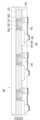
도 3은 본 발명의 바람직한 제1실시예에 따른 마이크로 LED 전사헤드(1000)가 마이크로 LED(100)를 진공으로 흡착한 상태를 도시한 도면이다. 본 발명의 제1실시예에 따른 마이크로 LED 전사헤드(1000)는, 기공을 갖는 다공성 부재(1100) 및 다공성 부재(1100)의 표면에 형성된 히터부(1001)를 포함한다.3 is a view showing a state in which the micro
바람직한 제1실시예에 따른 마이크로 LED 전사헤드(1000)는 제1기판(예를 들어, 성장기판(101))에서 제2기판(예를 들어, 표시 기판(300))으로 이송하는 전사헤드일 수 있다.The micro
다공성 부재(1100)의 상부에는 공기 챔버(1200)가 구비된다. 공기 챔버(1200)는 진공펌프에 연결된다. 공기 챔버(1200)는 진공펌프의 작동에 따라 다공성 부재(1100)의 다수의 기공에 진공을 가하거나 기공에 가하진 진공을 해제하는 기능을 한다. 공기 챔버(1200)를 다공성 부재(1100)에 결합하는 구조는 다공성 부재(1100)에 진공을 가하거나 가해진 진공을 해제함에 있어서 다른 부위로의 진공의 누설을 방지하는데 적절한 구조라면 이에 대한 한정은 없다.An
마이크로 LED(100)의 진공 흡착 시, 공기 챔버(1200)에 가해진 진공은 다공성 부재(1100)의 다수의 기공에 전달되어 마이크로 LED(100)에 대한 진공 흡착력이 발생한다. 한편, 마이크로 LED(100)의 탈착 시에는, 공기 챔버(1200)에 가해진 진공이 해제됨에 따라 다공성 부재(1100)의 다수의 기공에도 진공이 해제되어 마이크로 LED(100)에 대한 진공 흡착력이 제거된다.When the
다공성 부재(1100)는 내부에 기공이 다수 함유되어 있는 물질을 포함하여 구성되며, 일정 배열 또는 무질서한 기공구조로 0.2~0.95 정도의 기공도를 가지는 분말, 박막/후막 및 벌크 형태로 구성될 수 있다. 다공성 부재(1100)의 기공은 그 크기에 따라 직경 2 nm 이하의 마이크로(micro)기공, 2~50 nm 메조(meso)기공, 50 nm 이상의 마크로(macro)기공으로 구분할 수 있는데, 이들의 기공들을 적어도 일부를 포함한다. 다공성 부재(1100)는 그 구성 성분에 따라서 유기, 무기(세라믹), 금속, 하이브리드형 다공성 소재로 구분이 가능하다. 다공성 부재(1100)는 기공이 일정 배열로 형성되는 양극산화막을 포함한다. 다공성 부재(1100)는 형상의 측면에서 분말, 코팅막, 벌크가 가능하고, 분말의 경우 구형, 중공구형, 화이버, 튜브형등 다양한 형상이 가능하며, 분말을 그대로 사용하는 경우도 있지만, 이를 출발물질로 코팅막, 벌크 형상을 제조하여 사용하는 것도 가능하다.The
다공성 부재(1100)의 기공이 무질서한 기공구조를 갖는 경우에는, 다공성 부재(1100)의 내부는 다수의 기공들이 서로 연결되면서 다공성 부재(1100)의 상, 하를 연결하는 공기 유로를 형성하게 된다. 한편, 다공성 부재(1100)의 기공이 수직 형상의 기공구조를 갖는 경우에는, 다공성 부재(1100)의 내부는 수직 형상의 기공에 의해 다공성 부재(1100)의 상, 하로 관통되면서 공기 유로를 형성할 수 있도록 한다.When the pores of the
다공성 부재(1100)는 마이크로 LED(100)를 흡착하는 흡착영역(1310)과 마이크로 LED(100)를 흡착하지 않는 비흡착영역(1330)을 포함한다. 흡착영역(1310)은 공기 챔버(1200)의 진공이 전달되어 마이크로 LED(100)를 흡착하는 영역이고, 비흡착영역(1330)은 공기 챔버(1200)의 진공이 전달되지 않음에 따라 마이크로 LED(100)를 흡착하지 않는 영역이다.The
비흡착영역(1330)은 다공성 부재(1100)의 적어도 일부 표면에 차폐부를 형성함으로써 구현될 수 있다. 위와 같은 차폐부는 다공성 부재(1100)의 적어도 일부 표면에 형성된 기공을 막도록 형성된다. 차폐부는 다공성 부재(1100)의 상, 하 표면 중에서 적어도 일부 표면에 형성될 수 있고, 특히 다공성 부재(1100)의 기공 구조가 무질서한 기공 구조인 경우에는 다공성 부재(1100)의 상, 하 표면 모두에 형성될 수 있다.The
차폐부는 다공성 부재(1100)의 표면의 기공을 막는 기능을 수행할 수 있는 것이라면 그 재질, 형상, 두께에는 한정이 없다. 바람직하게는 포토레지스트(PR, Dry Film PR포함) 또는 금속 재질로 추가로 형성될 수 있고, 다공성 부재(1100)를 이루는 자체 구성에 의해서도 형성 가능하다. 여기서 다공성 부재(1100)를 이루는 자체 구성으로는, 예를 들어 후술하는 다공성 부재(1100)가 양극산화막으로 구성될 경우에는, 차폐부는 배리어층 또는 금속 모재일 수 있다.The material, shape, and thickness of the shielding unit are not limited as long as it can perform a function of blocking pores on the surface of the
전사헤드(1000)는 공기 챔버(1200)의 진공도를 모니터링하는 모니터링부가 구비될 수 있다. 모니터링부는 공기 챔버(1200)에 형성되는 진공도를 모니터링하며, 제어부는 공기 챔버(1200)의 진공도의 정도에 따라 공기 챔버(1200)의 진공도를 제어할 수 있다. 모니터링부에서 공기 챔버(1200)의 진공도가 기 설정된 진공도의 범위보다 낮은 진공도로 형성될 경우에는, 제어부는 다공성 부재(1100)에 진공 흡착되어야 하는 마이크로 LED(100) 중 일부가 진공 흡착되지 않은 경우로 판단하거나 일부에서 진공의 누설이 있는 것으로 판단하여 전사헤드(1000)의 재작동을 명령할 수 있다. 이처럼 공기 챔버(1200) 내부의 진공도의 정도에 따라 전사헤드(1000)가 마이크로 LED(100)를 오류 없이 이송하도록 한다.The
또한 전사헤드(1000)에는 다공성 부재(1100)와 마이크로 LED(100)간의 접촉을 완충시키기 위하여 완충 부재가 구비될 수 있다. 이러한 완충 부재는 다공성 부재(1100)와 마이크로 LED(100)간의 접촉을 완충하면서 탄성 복원력을 갖는 것이라면 그 재질에는 제한이 없다. 완충 부재는 다공성 부재(1100)와 공기 챔버(1200)의 사이에 형성될 수 있으나, 완충 부재의 설치 위치는 이에 한정되는 것은 아니다. 다공성 부재(1100)와 마이크로 LED(100)간의 접촉을 완충시킬 수 있는 위치라면, 완충 부재는 전사헤드(1000)의 어느 위치에 설치되어도 무관하다.In addition, a buffer member may be provided in the
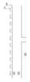
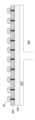
도 4는 다공성 부재(1100)의 하부면의 일부를 도시한 도면이다. 마이크로 LED(100)의 개수에 대응되어 발열부(2300)가 형성되지만, 도 4는 그 중 일부만을 편의상 도시한 것이다.FIG. 4 is a view showing a part of the lower surface of the
도 4를 참조하면, 히터부(1001)는 다공성 부재(1100)의 하부 표면에 형성된다. 히터부(1001)는, 전압이 인가되는 제1,2패드(2501, 2503), 마이크로 LED(100)의 흡착 위치에 대응되는 위치에 형성되는 발열부(2300), 제1,2패드(2501, 2503)와 발열부(2300) 및 발열부(2300)간을 연결하는 연결부(2400)로 구성된다. 전압이 제1,2패드(2501, 2503)에 인가되면 발열부(2300)는 전기에너지를 열에너지로 변환한다. 이를 통해 마이크로 LED(100)의 상면을 가열할 수 있다.Referring to FIG. 4 , the
발열부(2300)는 밀폐형 루프의 형상을 가질 수 있다. 도 4에 도시된 바와 같이 밀폐형 루프는 원형의 고리 형상으로 이루어질 수 있으며, 다각형의 고리형상으로 이루어 질 수 있다. 한편 발열부(2300)의 형상은 이에 한정되는 것은 아니며, 전기를 인가받아 전기에너지를 열에너지를 변환하기에 적절한 형상인 경우라면 본원 발명의 발열부(2300)의 범주에 포함될 수 있다.The
발열부(2300)와 발열부(2300)사이에는 연결부(2400)가 구성된다. 연결부(2400)는 발열부(2300) 사이를 서로 전기적으로 연결하여 발열부(2300)에 전기를 연결시켜주는 기능을 한다. 또한 연결부(2400)는 최외곽 발열부(2300)와 제1,2패드(2501, 2503)간을 전기적으로 연결하는 기능을 한다.A
다공성 부재(1100)의 표면에 형성된 기공(1350)은 흡입력으로 마이크로 LED(100)를 흡착한다. 이 경우 발열부(2300)의 내부로는 다공성 부재(1100)의 표면에 형성된 기공(1350)이 노출된다. 발열부(2300) 내부의 기공(1350)을 이용하여 마이크로 LED(100)를 흡착하며, 발열부(2300)에 의해 마이크로 LED(100)의 상면을 가열할 수 있게 된다.The
전술한 차폐부는 가림부(2600)로 구성될 수 있다. 다공성 부재(1100)의 하부표면은 발열부(2300)의 내부를 제외하고 가림부(2600)에 의해 다공성 부재(1100)의 기공(1350)을 막도록 형성될 수 있다. 즉, 다공성 부재(1100)의 하부 표면의 기공(1350)은 발열부(2300)의 내부를 제외하고 노출되지 않는다. 이러한 구성을 통해 발열부(2300) 내부에 형성되는 흡착영역(2100)에만 흡입력이 발생하며, 발열부(2300) 외부로는 흡입력이 발생하지 않는다. 흡착영역(2100)은 기공(1350)에 가하진 진공을 이용하여 마이크로 LED(100)를 진공흡착하여 전사할 수 있게 된다. 가림부(2600)를 통해 흡착영역(2100)을 제외한 영역의 기공(1350)이 모두 밀폐되어 공기 챔버(1200)의 진공압이 흡착영역(2100)으로 집중되므로 마이크로 LED(100)를 보다 쉽게 진공흡착할 수 있게 된다.The aforementioned shielding unit may be configured as the
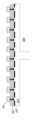
도 5는 마이크로 LED(100)가 다공성 부재(1100)의 하부표면에 흡착된 상태를 도시한 도면이다. 흡착영역(2100) 각각은 각각의 마이크로 LED(100)를 진공 흡착하며, 발열부(2300)는 흡착영역(2100)의 테두리에 형성되어 마이크로 LED(100)의 상면을 가열할 수 있게 된다.FIG. 5 is a view showing a state in which the
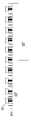
도 6은 도 4에 도시된 다공성 부재(1100)의 하부 표면의 변형례로서, 도 4의 가림부(2600)가 형성되지 않은 것이다. 도 4에 도시된 구조와는 달리 가림부(2600)가 형성되지 않은 구성이라는 점에서, 흡착영역(2100)에서의 진공압이 상대적으로 저하되기는 하나, 흡착영역(2100) 이외의 영역에서도 마이크로 LED(100)를 흡착할 수 있기 때문에 마이크로 LED(100)의 정렬오차가 있다고 하더라도 마이크로 LED(100)를 전사할 수 있는 효과를 발휘할 수 있게 된다.FIG. 6 is a modified example of the lower surface of the
도 7은 마이크로 LED(100)를 흡착한 전사헤드(1000)가 제2기판(300)에 마이크로 LED(100)를 전사하는 상태를 도시한 도면이다. 도 7을 참조하면, 전사헤드(1000)는 마이크로 LED(100)를 표시기판(300)의 제1 전극(510)에 전사한다.FIG. 7 is a diagram showing a state in which the
그런 다음 전사헤드(1000)의 히터부(1001)에 전기를 인가하여 발열부(2300)를 가열하게 된다. 이와 함께, 표시기판(300)에 전원을 인가하여 표시기판(300)의 제1전극(510)을 가열한다.Then, electricity is applied to the
마이크로 LED(100)를 표시기판(300)의 제1전극(510)에 본딩시키기 위한 수단으로 금속 접합방식을 이용할 수 있다. 금속 접합방식은 본딩 금속(합금)를 가열하여 용융상태에서 마이크로 LED(100)를 제1전극(510)에 접합하는 방식이며, 열압착 본딩 또는 유테틱 본딩 등을 이용할 수 있다.A metal bonding method may be used as a means for bonding the
마이크로 LED(100)를 표시기판(300) 등에 접합할 때, 표시기판(300)만을 가열하여 접합을 할 경우에는 냉납 문제가 발생할 수 있다. 다시 말해 표시기판(300)만을 가열하여 접합을 할 경우에는 본딩 금속(합금)의 상부 표면으로 갈수록 온도가 상대적으로 낮아지게 되어 냉납 문제가 발생하며 이로 인해 마이크로 LED(100)가 제1전극(510)에 견고하게 접합되지 않게 되는 문제점이 있다.When bonding the
하지만 본 발명의 바람직한 실시예에 따르면, 표시기판(300)을 통해 본딩 금속(합금)을 가열할 수 있을 뿐만 아니라 전사헤드(1000)의 히터부(1001)를 통해 마이크로 LED(100)의 상면을 가열할 수 있게 된다. 이를 통해 본딩 금속(합금)의 온도 분포가 본딩 금속(합금)의 깊이에 따라 균일화되므로 냉납 문제가 발생하지 않게 되고, 그 결과 마이크로 LED(100)가 표시기판(300)의 제1전극(510)에 보다 견고하게 접합된다.However, according to a preferred embodiment of the present invention, not only can the bonding metal (alloy) be heated through the
제2실시예Example 2
이하, 본 발명의 제2실시예에 대해 살펴본다.Hereinafter, look at the second embodiment of the present invention.
도 8은 본 발명의 바람직한 제2실시예에 따른 마이크로 LED 전사헤드(1000)를 도시한 도면이고, 도 9는 도 8의 ‘A’부분을 확대한 도면이고, 도 10은 제2실시예에 따른 마이크로 LED 전사헤드(1000)가 마이크로 LED(100)를 진공 흡착한 상태를 도시한 도면이다.8 is a view showing a micro
제2실시예에 따른 마이크로 LED 전사헤드(1000)는, 금속을 양극산화하여 형성된 기공을 갖는 양극산화막(1300)을 포함하여 구성된다는 것을 특징으로 한다.The micro
양극산화막(1300)의 하부에는 히터부(1001)가 구비된다. 히터부(1001)는 전기 전도성 재질이면 그 재질에는 한정이 없다. 히터부(1001)는 양극산화막(1300)의 표면에 스퍼터링(sputtering)공정을 통해 증착되어 형성될 수 있다. 히터부(1001)는 양극산화막(1300)의 기공(1303)을 막지 않는 구성으로 형성될 수 있다. 다시 말해 히터부(1001)는 양극산화막(1300)의 기공(1303)을 제외한 표면 상에 얇게 형성된다.A
히터부(1001)가 양극산화막(1300)의 표면에서 양극산화막(1300)의 표면에 형성되는 기공(1303)을 막지 않으면서 형성되는 구성에 따르면, 마이크로 LED(100)와 접촉되는 전사헤드(1000)의 접착면에는 양극산화막(1300)의 기공(1303)과 연통되는 구멍이 히터부(1001)에도 구비되므로, 양극산화막(1300)의 기공(1303)에 진공을 가하거나 기공(1303)에 가하진 진공을 해제하여 마이크로 LED(100)를 흡착하거나 흡착을 해제할 수 있다.According to the configuration in which the
양극산화막(1300)은 모재인 금속을 양극산화하여 형성된 막을 의미하고, 기공(1303)은 금속을 양극산화하여 양극산화막(1300)을 형성하는 과정에서 형성되는 구멍을 의미한다. 예컨대, 모재인 금속이 알루미늄(Al) 또는 알루미늄 합금인 경우, 모재를 양극산화하면 모재의 표면에 양극산화알루미늄(Al2O3) 재질의 양극산화막(1300)이 형성된다. 위와 같이, 형성된 양극산화막(1300)은 내부에 기공(1303)이 형성되지 않은 배리어층(1301)과, 내부에 기공(1303)이 형성된 다공층(1305)으로 구분된다. 배리어층(1301)은 모재의 상부에 위치하고, 다공층(1305)은 배리어층(1301)의 상부에 위치한다. 이처럼, 배리어층(1301)과 다공층(1305)을 갖는 양극산화막(1300)이 표면에 형성된 모재에서, 모재를 제거하게 되면, 양극산화알루미늄(Al2O3) 재질의 양극산화막(1300)만이 남게 된다.The
양극산화막(1300)은, 지름이 균일하고, 수직한 형태로 형성되면서 규칙적인 배열을 갖는 기공(1303)을 갖게 된다. 따라서, 배리어층(1301)을 제거하면, 기공(1303)은 상, 하로 수직하게 관통된 구조를 갖게 되며, 이를 통해 수직한 방향으로 진공압을 형성하는 것이 용이하게 된다.The
양극산화막(1300)의 내부는 수직 형상의 기공(1303)에 의해 수직한 형태로의 공기 유로를 형성할 수 있게 된다. 기공(1303)의 내부 폭은 수 nm 내지 수 백nm의 크기를 갖는다. 예를 들어, 진공 흡착하고자 하는 마이크로 LED(100)의 사이즈가 30㎛ x 30㎛인 경우이고 기공(1303)의 내부 폭이 수 nm인 경우에는 대략 수 천만개의 기공(1303)을 이용하여 마이크로 LED(100)를 진공 흡착할 수 있게 된다. 한편, 진공 흡착하고자 하는 마이크로 LED(100)의 사이즈가 30㎛ x 30㎛인 경우이고 기공(1303)의 내부 폭이 수 백 nm인 경우에는 대략 수 만개의 기공(1303)을 이용하여 마이크로 LED(100)를 진공 흡착할 수 있게 된다. 마이크로 LED(100)의 경우에는 기본적으로 제1 반도체층(102), 제2 반도체층(104), 제1 반도체층(102)과 제2 반도체층(104) 사이에 형성된 활성층(103), 제1 컨택전극(106) 및 제2 컨택전극(107)만으로 구성됨에 따라 상대적으로 가벼운 편이므로 양극산화막(1300)의 수만 내지 수 천만개의 기공(1303)을 이용하여 진공 흡착하는 것이 가능한 것이다.The inside of the
양극산화막(1300)의 상부에는 공기 챔버(1200)가 구비된다. 공기 챔버(1200)는 진공펌프에 연결된다. 공기 챔버(1200)는 진공펌프의 작동에 따라 양극산화막(1300)의 다수의 수직 형상의 기공에 진공을 가하거나 진공을 해제하는 기능을 한다.An
마이크로 LED(100)의 흡착 시, 공기 챔버(1200)에 가해진 진공은 양극산화막(1300)의 다수의 기공(1303)에 전달되어 마이크로 LED(100)에 대한 진공 흡착력을 제공한다. 한편, 마이크로 LED(100)의 탈착 시에는, 공기 챔버(1200)에 가해진 진공이 해제됨에 따라 양극산화막(1300)의 다수의 기공(1303)에도 진공이 해제되어 마이크로 LED(100)에 대한 진공 흡착력이 제거된다.When the
양극산화막(1300)은 마이크로 LED(100)를 진공 흡착하는 흡착영역(1310)과 마이크로 LED(100)를 흡착하지 않는 비흡착영역(1330)을 포함한다. 흡착영역(1310)은 공기 챔버(1200)의 진공이 전달되어 마이크로 LED(100)를 진공 흡착하는 영역이고, 비흡착영역(1330)은 공기 챔버(1200)의 진공이 전달되지 않음에 따라 마이크로 LED(100)를 흡착하지 않는 영역이다.The
바람직하게는, 흡착영역(1310)은 기공(1303)의 상, 하가 관통되는 영역이고, 비흡착영역(1330)은 기공(1303)의 상, 하 중 적어도 어느 한 부분이 폐쇄된 영역일 수 있다.Preferably, the
비흡착영역(1330)은 양극산화막(1300)의 적어도 일부 표면에 차폐부를 형성함으로써 구현될 수 있다. 위와 같은 차폐부는 양극산화막(1100)의 적어도 일부 표면으로 노출되는 기공(1303)의 입구를 막도록 형성된다. 차폐부는 양극산화막(1300)의 상, 하 표면 중에서 적어도 일부 표면에 형성될 수 있다. 차폐부는 다공성 부재(1100)의 표면으로 노출되는 기공(1303)의 입구를 막는 기능을 수행할 수 있는 것이라면 그 재질, 형상, 두께에는 한정이 없다. 바람직하게 차례부는 포토레지스트(PR, Dry Film PR포함) 또는 금속 재질로 추가로 형성될 수 있고, 배리어층(1301)일 수 있다.The
비흡착영역(1330)은 양극산화막(1310)의 제조 시 형성된 배리어층(1301)에 의해 수직 형상의 기공(1303)의 상, 하 중 어느 한 부분이 폐쇄되도록 하여 형성될 수 있고, 흡착영역(1310)은 에칭 등의 방법으로 배리어층(1301)이 제거되어 수직 형상의 기공(1303)의 상, 하가 서로 관통되도록 형성될 수 있다.The
또한 상, 하로 관통하는 기공(1303)은 배리어층(1301)의 일부가 제거됨에 따라 형성되므로, 흡착영역(1310)의 양극산화막(1300)의 두께는 비흡착영역(1330)의 양극산화막(1300)의 두께보다 작다.In addition, since the
도 8, 9에는, 배리어층(1301)이 양극산화막(1300)의 상부에 위치하고 기공(1303)이 있는 다공층(1305)이 하부에 위치하는 것으로 도시되어 있으나, 배리어층(1301)이 양극산화막(1300)의 하부에 위치하도록 도 8, 9에 도시된 양극산화막(1300)이 상, 하 반전되어 비흡착영역(1330)을 구성할 수 있다.8 and 9, it is shown that the
한편, 비흡착영역(1330)이 배리어층(1301)에 의해 기공(1303)의 상, 하 중 어느 한 부분이 폐쇄된 것으로 설명하였으나, 배리어층(1301)에 의해 폐쇄되지 않은 반대면은 별도의 코팅층이 추가되어 상, 하가 모두 폐쇄되도록 구성될 수 있다. 비흡착영역(1330)을 구성함에 있어서 양극산화막(1300)의 상, 하면이 모두 폐쇄되는 구성은, 양극산화막(1300)의 상, 하면 중 적어도 하나가 폐쇄되는 구성에 비해, 비흡착영역(1330)의 기공(1303)에 이물질이 잔존할 우려를 줄일 수 있다는 점에서 유리하다.On the other hand, although the
도 11에는 도 10에 도시된 마이크로 LED 전사헤드(1000)의 변형례가 도시되어 있다. 도 11에 도시된 전사헤드(1000)는, 비흡착영역(1330)의 상부에는 양극산화막(1300)의 강도를 보강하기 위한 지지부(1307)가 추가로 형성된다. 일례로, 지지부(1307)는 금속 재질의 모재가 될 수 있다. 양극산화 시 사용된 금속 재질의 모재가 제거되지 않고 배리어층(1301)의 상부에 구비되면서 금속 재질(예건대, 알루미늄 또는 알루미늄 합금)의 모재가 지지부(1307)가 될 수 있다.FIG. 11 shows a modified example of the micro
도 11를 참조하면, 비흡착영역(1330)에서는 금속 재질의 모재(1307), 배리어층(1301) 및 기공(1303)이 형성된 다공층(1305)이 모두 구비된 채로 형성되고, 흡착영역(1310)은 금속 재질의 모재(1307) 및 배리어층(1301)이 제거됨에 따라 기공(1303)의 상, 하가 관통되도록 형성된다. 금속 재질의 모재(1307)가 비흡착영역(1330)에 구비되어 양극산화막(1300)의 강성을 확보할 수 있게 된다. 위와 같은 지지부(1307)의 구성에 의하여, 상대적으로 강도가 약한 양극산화막(1300)의 강도를 높일 수 있게 됨에 따라 양극산화막(1300)으로 구성되는 전사헤드(1000)의 크기를 대면적화 할 수 있다.Referring to FIG. 11, in the
도 12(a)에는, 도 10에 도시된 전사헤드(1000)의 변형례가 도시되어 있다. 도 12(a)에 도시된 전사헤드(1000)는, 양극산화막(1300)의 흡착영역(1310)에는 양극산화막(1300)의 자연발생적으로 형성되는 기공(1303) 이외에 투과홀(1309)이 추가로 형성된다. 투과홀(1309)은 양극산화막(1300)의 상면과 하면을 관통하도록 형성된다. 투과홀(1309)의 직경은 기공(1303)의 직경보다 더 크게 형성된다. 기공(1303)의 직경보다 더 큰 직경을 갖는 투과홀(1309)이 형성되는 구성에 의하여, 기공(1303)만으로 마이크로 LED(100)를 진공 흡착하는 구성에 비해, 마이크로 LED(100)에 대한 진공 흡착면적을 키울 수 있게 된다.In FIG. 12(a), a modified example of the
이러한 투과홀(1309)은 전술한 양극산화막(1300) 및 기공(1303)이 형성된 후, 양극산화막(1300)을 수직방향으로 에칭함으로써 형성될 수 있다. 흡착영역(1310)에서의 진공 누설을 방지한다는 측면에서 투과홀(1309)은 흡착영역(1310)의 중심에 분포하는 것이 바람직하다.The
한편, 전사헤드(1000) 전체적인 관점에서 살펴보면, 투과홀(1309)은 각각의 흡착영역(1310)의 위치에 따라 그 크기 및 개수를 달리할 수 있다. 진공펌프가 전사헤드(1000)의 중심에 위치하는 경우에는, 전사헤드(1000)의 가장자리 측으로 갈수록 진공압이 감소되어 흡착영역(1310)간의 진공압의 불균일이 초래될 수 있다. 이런 경우에는 전사헤드(1000)의 가장자리 측으로 위치하는 흡착영역(1310) 내의 투과홀(1309)에 의해 형성되는 흡착 면적의 크기를, 전사헤드(1000)의 중심 측으로 위치하는 흡착영역(1310) 내의 투과홀(1309)에 의해 형성되는 흡착 면적의 크기보다 더 크게 형성할 수 있다. 이처럼 흡착영역(1310)의 위치에 따라 투과홀(1309)의 흡착면적의 크기에 변화를 줌으로써, 흡착영역(1310) 간에 발생하는 진공압의 불균일을 해소하여 균일한 진공 흡착력을 제공할 수 있다.Meanwhile, from the overall viewpoint of the
도 12(b)에는, 도 10에 도시된 전사헤드(1000)의 변형례가 도시되어 있다. 도 12(b)에 도시된 전사헤드(1000)는, 양극산화막(1300)의 흡착영역(1310)의 하부에는 흡착홈(1310)이 추가로 형성된다. 흡착홈(1310)은 전술한 기공(1303) 또는 투과홀(1309)보다 더 큰 수평 면적을 갖으면서도 마이크로 LED(100)의 상면의 수평 면적보다 작은 면적을 갖는다. 이를 통해 마이크로 LED(100)에 대한 진공 흡착 면적을 더 키울 수 있게 되고, 흡착홈(1310)을 통해 마이크로 LED(100)에 대한 균일한 진공 흡착 면적을 제공할 수 있게 된다. 흡착홈(1310)은 전술한 양극산화막(1300) 및 기공(1303)이 형성된 후, 양극산화막(1300)의 일부를 소정의 깊이로 에칭함으로써 형성될 수 있다.In FIG. 12(b), a modified example of the
제3실시예3rd embodiment
이하, 본 발명의 제3실시예에 대해 살펴본다.Hereinafter, look at the third embodiment of the present invention.
도 13는 본 발명의 바람직한 제3실시예에 따른 마이크로 LED 전사헤드(1000)를 도시한 도면이다.13 is a diagram showing a micro
제3실시예에 따른 마이크로 LED 전사헤드(1000)는, 제1,2다공성부재(1500, 1600)의 이중 구조를 포함하여 구성된다는 것을 특징으로 한다.The micro
제1다공성 부재(1500)의 하부에는 히터부(1001)이 구비된다. 제1다공성 부재(1500)의 표면에 형성되는 히터부(1001)는 다공성 부재(1100)의 표면에 형성되는 기공을 막지 않는 형태로 구성된다.A
제1다공성 부재(1500)의 상부에는 제2다공성 부재(1600)가 구비된다. 제1다공성 부재(1500)는 마이크로 LED(100)를 진공 흡착하는 기능을 수행하는 구성이고, 제2다공성 부재(1600)는 공기 챔버(1200)와 제1다공성 부재(1500) 사이에 위치하여 공기 챔버(1200)의 진공압을 제1다공성 부재(1500)에 전달하는 기능을 수행한다.A second
제1,2다공성 부재(1500, 1600)은 서로 다른 다공성의 특성을 가질 수 있다. 예를 들어, 제1,2다공성 부재(1500, 1600)는 기공의 배열 및 크기, 다공성 부재의 소재, 형상 등에서 서로 다른 특성을 가진다.The first and second
기공의 배열 측면에서 살펴보면, 제1,2다공성 부재(1500, 1600) 중 하나는 기공이 일정한 배열을 갖는 것이고 다른 하나는 기공이 무질서한 배열을 갖는 것일 수 있다. 기공의 크기 측면에서 살펴보면, 제1,2다공성 부재(1500,1600) 중 어느 하나는 기공의 크기가 다른 하나에 비해 큰 것일 수 있다. 여기서 기공의 크기는 기공의 평균 크기일 수 있고, 기공 중에서의 최대 크기일 수 있다. 다공성 부재의 소재 측면에서 살펴보면, 어느 하나가 유기, 무기(세라믹), 금속, 하이브리드형 다공성 소재 중 하나의 소재로 구성되면 다른 하나는 어느 하나의 소재와는 다른 소재로서 유기, 무기(세라믹), 금속, 하이브리드형 다공성 소재 중에서 선택될 수 있다. 다공성 부재의 형상 측면에서 살펴보면, 제1,2다공성 부재(1500, 1600)의 형상은 서로 상이하게 구성될 수 있다.In terms of the arrangement of pores, one of the first and second
이처럼 제1,2다공성 부재(1500,1600)의 기공의 배열 및 크기, 소재 및 형상 등을 서로 달리함으로써 전사헤드(1000)의 기능을 다양하게 할 수 있고, 제1,2다공성 부재(1500, 1600)의 각각에 대한 상보적인 기능을 수행할 수 있게 할 수 있다. 다공성 부재의 개수는 제1,2다공성 부재처럼 2개로 한정되는 것은 아니며 각각의 다공성 부재가 서로 상보적인 기능을 갖는 것이라면 그 이상으로 구비되는 것도 제3실시예의 범위에 포함된다.As described above, the function of the
도 14를 참조하면, 제1다공성 부재(1500)는 전술한 제2실시예 및 그 변형례의 구성으로 구비될 수 있다. 제1다공성 부재(1500)의 하부에는 히터부(1001)가 구비된다. 히터부(1001)는 제1다공성 부재(1500)의 하부 표면에 형성된 기공을 막지 않으면서 소정의 두께를 가지면서 형성된다.Referring to FIG. 14 , the first
제2다공성 부재(1600)은 제1다공성 부재(1500)를 지지하는 기능을 갖는 다공성 지지체로 구성될 수 있다. 제2다공성 부재(1600)가 제1다공성 부재(1500)를 지지하는 기능을 달성할 수 있는 구성이라면 그 재료에는 한정이 없으며, 전술한 제1실시예의 다공성 부재(1100)의 구성이 포함될 수 있다. 제2다공성 부재(1600)는 제1다공성 부재(1500)의 중앙 처짐 현상 방지에 효과를 갖는 경질의 다공성 지지체로 구성될 수 있다. 예컨대, 제2다공성 부재(1600)는 다공성 세라믹 소재일 수 있다.The second
다공성 세라믹 소재의 경우, 다공성 기공의 크기가 불균일하고, 여러 방향에서 기공이 형성되어 있어 위치에 따른 진공압이 불균일하게 형성될 수 있다. 이와 달리, 양극산화막은 크기가 균일하고, 기공의 방향이 일방향(예컨데, 상하 방향)으로 형성되어 있으므로, 위치가 다르더라도 진공압이 균일하게 형성된다. 따라서, 전술한 바와 같이, 제1다공성부재(1500)가 기공을 갖는 양극산화막으로 구성되고, 제2다공성 부재(1600)가 다공성 세라믹 소재로 구성되면, 전사헤드(1000)의 다공성을 유지하면서 강성을 확보할 수 있을 뿐만 아니라, 진공압의 균일성을 확보할 수 있게 된다.In the case of a porous ceramic material, the size of porous pores is non-uniform and pores are formed in various directions, so that vacuum pressure may be non-uniform depending on the location. Unlike this, since the size of the anodic oxide film is uniform and the pores are formed in one direction (eg, vertical direction), vacuum pressure is uniformly formed even if the location is different. Therefore, as described above, when the first
한편, 제1다공성 부재(1500)는 전술한 제2실시예 및 그 변형례의 구성으로 구비되면서, 제2다공성 부재(1600)는 제1다공성 부재(1500)와 마이크로 LED(100)간의 접촉시 이를 완충하기 위한 다공성 완충체로 구성될 수 있다. 제2다공성 부재(1600)가 제1다공성 부재(1500)를 완충하는 기능을 달성할 수 있는 구성이라면 그 재료에는 한정이 없으며, 전술한 제1실시예의 다공성 부재(1100)의 구성이 포함될 수 있다. 제2다공성 부재(1600)는 제1다공성 부재(1500)가 마이크로 LED(100)와 접촉되어 진공으로 마이크로 LED(100)를 흡착하는 경우에 제1다공성 부재(1500)가 마이크로 LED(100)에 맞닿아 마이크로 LED(100)를 손상시키는 것을 방지하는데 도움이 되는 연질의 다공성 완충체로 구성될 수 있다. 예컨대, 제2다공성 부재(1600)는 스펀지 등과 같은 다공성 탄성 재질일 수 있다.On the other hand, while the first
제4실시예Example 4
이하, 본 발명의 제4실시예에 대해 살펴본다.Hereinafter, look at the fourth embodiment of the present invention.
도 15은 본 발명의 바람직한 제4실시예에 따른 마이크로 LED 전사헤드(1000)를 도시한 도면이다.15 is a diagram showing a micro
제4실시예에 따른 마이크로 LED 전사헤드(1000)는, 제1,2,3다공성부재(1700, 1800, 1900)의 삼중 구조를 포함하여 구성된다는 것을 특징으로 한다.The micro
제1다공성 부재(1500)의 하부에는 히터부(1001)이 구비된다. 히터부(1001)는 제1다공성 부재(1500)의 하부 표면에 형성된 기공을 막지 않으면서 소정의 두께를 가지면서 형성된다.A
제1다공성 부재(1700)의 상부에는 제2다공성 부재(1800)가 구비되고, 제2다공성 부재(1800)의 상부에는 제3다공성 부재(1900)가 구비된다. 제1다공성 부재(1700)는 마이크로 LED(100)를 진공 흡착하는 기능을 수행하는 구성이다. 제2다공성 부재(1800) 및 제3다공성 부재(1900) 중 적어도 하는 경질의 다공성 지지체이고 다른 하나는 연질의 다공성 완충체로 구성될 수 있다.A second
제1다공성 부재(1700)은 제2실시예 및 그변형례의 구성으로 구비될 수 있고, 제2다공성 부재(1800)은 제1다공성 부재(1500)의 중앙 처짐 현상 방지에 효과를 갖는 경질의 다공성 지지체로 구성될 수 있으며(예컨대, 다공성 세라믹 소재), 제3다공성 부재(1900)는 연질의 다공성 완충체(예컨대, 스펀지 소재등과 같이 탄력이 높으면서 다공성인 소재)로 구성될 수 있다.The first
위와 같은 구성에 의하여, 다수의 마이크로 LED(100)에 대해 균일하게 진공 흡착할 수 있고, 제1다공성 부재(1700)의 중앙 처짐 현상을 방지할 수 있을 뿐만 아니라 마이크로 LED(100)의 손상을 방지할 수 있는 효과를 갖는다.With the above configuration, it is possible to uniformly vacuum adsorb the plurality of
제5실시예Example 5
이하, 본 발명의 제5실시예에 대해 살펴본다. 본 발명의 제5실시예에 따른 마이크로 LED 전사헤드(1000)는, 기공을 갖는 다공성 부재(1300), 다공성 부재를 수직하게 관통하는 수직전도부 및 수직전도부와 연결되는 수평 전도부를 포함한다.Hereinafter, look at the fifth embodiment of the present invention. The micro
다공성 부재를 수직하게 관통하여 형성되는 수직전도부 및 수직전도부와 연결되어 표면측으로 노출되는 수평 전도부를 포함하는 히터부의 구성을 통해, 마이크로 LED(100)의 상면을 가열할 수 있다.The upper surface of the
수직전도부(1351) 및 수직전도부(1351)와 연결되어 표면측으로 노출되는 수평전도부(1353)의 구성은 흡착영역(1310) 내에 구비될 수 있고, 비흡착영역(1330) 내에 구비될 수 있다. 다만, 수직전도부(1351) 및 수평전도부(1353)의 구성이 흡착영역(1310) 내에 구비되는 구성에 의하면, 마이크로 LED(100)를 흡착한 상태에서 히터부(1001)에 전기를 인가할 수 있다.The configuration of the vertical
도 17a, 17b를 참조하면, 흡착영역(1310)은 배리어층(1301)이 제거되어 기공(1303)의 상, 하가 관통되어 구성을 포함한다.Referring to FIGS. 17A and 17B , the
이러한 흡착영역(1310)은 흡착부(a)와 히터부(b)를 포함한다.The
흡착부(a)는 기공(1303)이 상, 하로 관통되는 부분으로서, 마이크로 LED(100)를 흡착하는 부분이며, 히터부(b)는 전도성 물질로 구성되는 부분이다.The adsorbing part (a) is a part through which the
수평전도부(1353)는 전사헤드(1000)가 마이크로 LED(100)를 흡착하는 흡착면의 반대면에 형성된다. 수직전도부(1351)는 마이크로 LED(100)가 흡착되는 흡착영역(1310) 내에 위치하게 된다. 수직전도부(1351)는 양극산화막(1300)의 기공(1303)에 충진되어 형성되며, 그 일단은 수평전도부(1353)와 일체로 연결되고 그 타단은 마이크로 LED(100)의 흡착면에 노출되게 형성된다.The horizontal
이를 통해 흡착영역(1310)은 마이크로 LED(100)를 흡착함과 동시에 그 흡착면에 수직전도부(b)가 접촉함으로써 마이크로 LED(100)의 상면 가열이 가능하게 된다.Through this, the
도 17b는 도 17a의 'A'부분의 양극산화막(1300)의 상부에서 바라본 도면이며, 도 17b를 참조하면, 개구된 형태의 흡착영역(1310)이 형성되고 흡착영역(1310)의 주면으로는 배리어층(1301)에 의해 비흡착영역(1330)이 형성된다.FIG. 17B is a view from the top of the
계속해서 도 17b를 참조하면, 수평전도부(1353)는 흡착영역(1310)의 범위내에서 상, 하로 관통되는 기공(1303)의 일부만을 덮는 형태로 구성되고, 수평전도부(1353)에 의해 덮히지 않는 기공(1303)은 마이크로 LED(100)를 흡착하는 기능을 하게 된다.Continuing to refer to FIG. 17B, the horizontal
또한 나란하게 배치되는 각각의 수평전도부(1353)를 공통적으로 연결하는 공통히터부(1355)이 양극산화막(1300)의 일측에 구비될 수 있다. 하나의 공통히터부(1355)에 복수 개의 수평전도부(1353)가 연결되는 구성이다. 이러한 공통히터부(1355)의 구성을 통해 나란하게 배치되는 각각의 수평전도부(1353)를 일괄적으로 연결할 수 있게 된다.In addition, a
도 18에는 도 16에 도시된 마이크로 LED 전사헤드(1000)의 변형례가 도시되어 있다. 도 18에 도시된 전사헤드(1000)는, 비흡착영역(1330)의 상부에는 양극산화막(1300)의 강도를 보강하기 위한 지지부(1307)가 추가로 형성된다. 일례로, 지지부(1307)는 금속 재질의 모재가 될 수 있다. 양극산화 시 사용된 금속 재질의 모재가 제거되지 않고 배리어층(1301)의 상부에 구비되면서 금속 재질(예건대, 알루미늄 또는 알루미늄 합금)의 모재가 지지부(1307)가 될 수 있다. 도 18을 참조하면, 비흡착영역(1330)에서는 금속 재질의 모재(1307), 배리어층(1301) 및 기공(1303)이 형성된 다공층(1305)이 모두 구비된 채로 형성되고, 흡착영역(1310)은 금속 재질의 모재(1307) 및 배리어층(1301)이 제거됨에 따라 기공(1303)의 상, 하가 관통되도록 형성된다. 금속 재질의 모재(1307)가 비흡착영역(1330)에 구비되어 양극산화막(1300)의 강성을 확보할 수 있게 된다. 위와 같은 지지부(1307)의 구성에 의하여, 상대적으로 강도가 약한 양극산화막(1300)의 강도를 높일 수 있게 됨에 따라 양극산화막(1300)으로 구성되는 마이크로 LED 전사헤드(1000)의 크기를 대면적화 할 수 있다.FIG. 18 shows a modified example of the micro
도 19는, 도 16에 도시된 전사헤드(1000)의 변형례가 도시되어 있다. 도 19에 도시된 전사헤드(1000)는, 양극산화막(1300)의 흡착영역(1310)에는 양극산화막(1300)의 자연발생적으로 형성되는 기공(1303) 이외에 투과홀(1309)이 추가로 형성된다. 투과홀(1309)은 양극산화막(1300)의 상면과 하면을 관통하도록 형성된다. 투과홀(1309)의 직경은 기공(1303)의 직경보다 더 크게 형성된다. 이러한 투과홀(1309)은 전술한 양극산화막(1300) 및 기공(1303)이 형성된 후, 양극산화막(1300)을 수직방향으로 에칭함으로써 형성될 수 있다. 투과홀(1309)이 에칭에 의해 형성됨으로써, 단순히 기공(1303)을 확공하여 투과홀(1309)을 형성하는 것보다 더욱 안정적으로 투과홀(1309)을 형성시킬 수 있다. 이러한 투과홀(1309)을 이용하여 수직전도부(1351)을 형성을 보다 쉽게 구현할 수 있고, 마이크로 LED(100)와 수직전도부(1351)의 접촉면적을 키울 수 있게 된다.FIG. 19 shows a modified example of the
제6실시예6th embodiment
이하, 본 발명의 제6실시예에 대해 살펴본다.Hereinafter, look at the sixth embodiment of the present invention.
도 20은 본 발명의 바람직한 제6실시예에 따른 마이크로 LED 전사헤드(1000)를 도시한 도면이다.20 is a diagram showing a micro
제6실시예에 따른 마이크로 LED 전사헤드(1000)는, 제1,2다공성부재(1500, 1600)의 이중 구조를 포함하여 구성된다는 것을 특징으로 한다. 제1다공성 부재(1500)의 상부에는 제2다공성 부재(1600)가 구비된다.The micro
제1다공성 부재(1500)는 마이크로 LED(100)를 진공 흡착하는 기능을 수행하고, 제2다공성 부재(1600)는 공기 챔버(1200)와 제1다공성 부재(1500) 사이에 위치하여 공기 챔버(1200)의 진공압을 제1다공성 부재(1500)에 전달하는 기능을 수행한다.The first
제1다공성 부재(1500)는 금속을 양극산화하여 형성된 기공을 갖는 양극산화막으로 구비된다. 제1다공성 부재(1500)에는 제1다공성 부재(1500)를 수직하게 관통하는 수직전도부(1351) 및 수직전도부(1351)와 연결되는 수평전도부(1353)를 포함하는 히터부(1001)가 구비된다.The first
제2다공성 부재(1600)은 제1다공성 부재(1500)를 지지하는 기능을 갖는 다공성 지지체로 구성될 수 있다. 제2다공성 부재(1600)가 제1다공성 부재(1500)를 지지하는 기능을 달성할 수 있는 구성이라면 그 재료에는 한정이 없다.The second
제2다공성 부재(1600)는 제1다공성 부재(1500)의 중앙 처짐 현상 방지에 효과를 갖는 경질의 다공성 지지체로 구성될 수 있다. 예컨대, 제2다공성 부재(1600)는 다공성 세라믹 소재일 수 있다.The second
다공성 세라믹 소재의 경우, 다공성 기공의 크기가 불균일하고, 여러 방향에서 기공이 형성되어 있어 위치에 따른 진공압이 불균일하게 형성될 수 있다. 이와 달리, 양극산화막은 크기가 균일하고, 기공의 방향이 일방향(예컨데, 상하 방향)으로 형성되어 있으므로, 위치가 다르더라도 진공압이 균일하게 형성된다.In the case of a porous ceramic material, the size of porous pores is non-uniform and pores are formed in various directions, so that vacuum pressure may be non-uniform depending on the location. Unlike this, since the size of the anodic oxide film is uniform and the pores are formed in one direction (eg, vertical direction), vacuum pressure is uniformly formed even if the location is different.
따라서, 전술한 바와 같이, 제1다공성부재(1500)가 기공을 갖는 양극산화막으로 구성되고, 제2다공성 부재(1600)가 다공성 세라믹 소재로 구성되면, 전사헤드(1000)의 다공성을 유지하면서 강성을 확보할 수 있을 뿐만 아니라, 진공압의 균일성을 확보할 수 있게 된다.Therefore, as described above, when the first
전술한 바와 같이, 본 발명의 바람직한 실시 예를 참조하여 설명하였지만, 해당 기술분야의 통상의 기술자는 하기의 특허 청구범위에 기재된 본 발명의 사상 및 영역으로부터 벗어나지 않는 범위 내에서 본 발명을 다양하게 수정 또는 변형하여 실시할 수 있다.As described above, although it has been described with reference to preferred embodiments of the present invention, those skilled in the art can variously modify the present invention within the scope not departing from the spirit and scope of the present invention described in the claims below. Or it can be carried out by modifying.
100: 마이크로 LED101: 성장기판
300: 표시기판1000: 전사헤드100: micro LED 101: growth substrate
300: display board 1000: transfer head
Claims (8)
Translated fromKorean상기 다공성 부재의 표면에 형성된 히터부를 포함하고,
상기 다공성 부재는 마이크로 LED를 흡착하는 흡착영역을 포함하고,
상기 히터부는 상기 흡착영역에 대응되어 각각 형성되는 것을 특징으로 하는 마이크로 LED 전사 헤드.
a porous member having pores; and
A heater part formed on the surface of the porous member,
The porous member includes an adsorption area for adsorbing the micro LED,
The micro LED transfer head, characterized in that the heater unit is formed to correspond to the adsorption area, respectively.
상기 히터부는 폐쇄형 루프로 구성되는 발열부를 포함하는 것을 특징으로 하는 마이크로 LED 전사 헤드.
According to claim 1,
The heater unit includes a heating unit configured as a closed loop micro LED transfer head.
상기 발열부의 내측으로 상기 흡착영역이 형성되는 것을 특징으로 하는 마이크로 LED 전사 헤드.
According to claim 3,
Micro LED transfer head, characterized in that the adsorption area is formed inside the heating part.
상기 히터부는 상기 다공성 부재 표면의 기공을 막지 않으면서 형성되는 것을 특징으로 하는 마이크로 LED 전사 헤드.
According to claim 1,
The micro LED transfer head, characterized in that the heater unit is formed without blocking pores on the surface of the porous member.
상기 다공성 부재의 표면에 형성된 히터부를 포함하고,
상기 히터부는,
상기 다공성 부재를 수직하게 관통하는 수직전도부; 및
상기 수직전도부와 연결되며, 상기 다공성 부재의 표면에 형성되는 수평전도부를 포함하는 것을 특징으로 하는 마이크로 LED 전사 헤드.
a porous member having pores; and
A heater part formed on the surface of the porous member,
the heater part,
a vertical conduction portion vertically penetrating the porous member; and
Micro LED transfer head, characterized in that it comprises a horizontal conductive portion connected to the vertical conductive portion and formed on the surface of the porous member.
상기 다공성 부재는 다공질 세라믹을 포함하는 것을 특징으로 하는 마이크로 LED 전사 헤드.
According to claim 1,
The micro LED transfer head, characterized in that the porous member comprises a porous ceramic.
상기 다공성 부재는 양극산화막을 포함하는 것을 특징으로 하는 마이크로 LED 전사 헤드.
According to claim 1,
The micro LED transfer head, characterized in that the porous member comprises an anodic oxide film.
Priority Applications (1)
| Application Number | Priority Date | Filing Date | Title |
|---|---|---|---|
| KR1020180048979AKR102498112B1 (en) | 2018-04-27 | 2018-04-27 | Micro led transfer head |
Applications Claiming Priority (1)
| Application Number | Priority Date | Filing Date | Title |
|---|---|---|---|
| KR1020180048979AKR102498112B1 (en) | 2018-04-27 | 2018-04-27 | Micro led transfer head |
Publications (2)
| Publication Number | Publication Date |
|---|---|
| KR20190124916A KR20190124916A (en) | 2019-11-06 |
| KR102498112B1true KR102498112B1 (en) | 2023-02-09 |
Family
ID=68541866
Family Applications (1)
| Application Number | Title | Priority Date | Filing Date |
|---|---|---|---|
| KR1020180048979AActiveKR102498112B1 (en) | 2018-04-27 | 2018-04-27 | Micro led transfer head |
Country Status (1)
| Country | Link |
|---|---|
| KR (1) | KR102498112B1 (en) |
Families Citing this family (2)
| Publication number | Priority date | Publication date | Assignee | Title |
|---|---|---|---|---|
| KR102524688B1 (en) | 2021-01-15 | 2023-04-21 | 김은일 | Multipurpose solar energy system and construction method thereof |
| KR102735772B1 (en) | 2021-10-16 | 2024-11-27 | 김은일 | Sheathing solar energy system and construction method thereof |
Citations (2)
| Publication number | Priority date | Publication date | Assignee | Title |
|---|---|---|---|---|
| JP2006225182A (en)* | 2005-02-15 | 2006-08-31 | Nichias Corp | Ceramic porous body heater and manufacturing method thereof |
| JP2014130996A (en) | 2012-11-30 | 2014-07-10 | Kyocera Corp | Heating carrier device |
Family Cites Families (10)
| Publication number | Priority date | Publication date | Assignee | Title |
|---|---|---|---|---|
| JP3596127B2 (en)* | 1995-12-04 | 2004-12-02 | ソニー株式会社 | Electrostatic chuck, thin plate holding device, semiconductor manufacturing device, transport method, and semiconductor manufacturing method |
| US6410942B1 (en) | 1999-12-03 | 2002-06-25 | Cree Lighting Company | Enhanced light extraction through the use of micro-LED arrays |
| KR101801264B1 (en)* | 2011-06-13 | 2017-11-27 | 삼성전자주식회사 | Apparatus of manufacturing semiconductor and Method for packaging semiconductor using the same |
| KR101596386B1 (en) | 2011-11-18 | 2016-02-22 | 애플 인크. | Method of forming a micro led structure and array of micro led structures with an electrically insulating layer |
| US9773750B2 (en)* | 2012-02-09 | 2017-09-26 | Apple Inc. | Method of transferring and bonding an array of micro devices |
| TWI697057B (en) | 2014-06-18 | 2020-06-21 | 愛爾蘭商艾克斯展示公司技術有限公司 | Systems and methods for controlling release of transferable semiconductor structures |
| KR101757404B1 (en) | 2015-07-24 | 2017-07-12 | 한국기계연구원 | Selective continuous transferring apparatus based on adhesion-controlled film |
| KR102402189B1 (en) | 2015-08-26 | 2022-05-25 | 엘지전자 주식회사 | Transfer unit for micro device |
| KR102465382B1 (en) | 2015-08-31 | 2022-11-10 | 삼성디스플레이 주식회사 | Diplay apparatus and manufacturing method for the same |
| KR101754528B1 (en) | 2016-03-23 | 2017-07-06 | 한국광기술원 | Transfer assembly with dry adhesion structure and method for transferring led structure assembly using the same and led structure assembly |
- 2018
- 2018-04-27KRKR1020180048979Apatent/KR102498112B1/enactiveActive
Patent Citations (2)
| Publication number | Priority date | Publication date | Assignee | Title |
|---|---|---|---|---|
| JP2006225182A (en)* | 2005-02-15 | 2006-08-31 | Nichias Corp | Ceramic porous body heater and manufacturing method thereof |
| JP2014130996A (en) | 2012-11-30 | 2014-07-10 | Kyocera Corp | Heating carrier device |
Also Published As
| Publication number | Publication date |
|---|---|
| KR20190124916A (en) | 2019-11-06 |
Similar Documents
| Publication | Publication Date | Title |
|---|---|---|
| KR102471582B1 (en) | Trnasfer head for micro led | |
| KR20190114372A (en) | Transfer system for micro led | |
| KR102517784B1 (en) | Micro led adsorption body | |
| KR20190114330A (en) | Transfer head for micro led | |
| KR20200025079A (en) | Transfer head | |
| KR20190131305A (en) | Micro led transfer system | |
| KR102527139B1 (en) | Transfer head for micro led and transfer stage for micro led | |
| KR102527138B1 (en) | Micro led transfer system | |
| KR20210020425A (en) | Transfer head for micro led | |
| KR102498112B1 (en) | Micro led transfer head | |
| TW201944086A (en) | Micro LED adsorption body | |
| KR102481434B1 (en) | Transfer head and adsorbing method for micro led using the same | |
| KR20200001323A (en) | Transfer head for micro led | |
| KR102643764B1 (en) | Transfer head for micro led | |
| KR102498109B1 (en) | Micro led transfer system | |
| KR102540860B1 (en) | Transfer head for micro led and micro led transfer system using the same | |
| KR102540859B1 (en) | Transfer head for micro led and micro led transfer system using the same | |
| KR20200005234A (en) | Transfer head for micro led | |
| KR102498037B1 (en) | Micro led adsorption body | |
| CN110648956A (en) | Micro light emitting diode transfer head | |
| KR102471583B1 (en) | Micro led transfer system including micro led adsorption body | |
| KR102471585B1 (en) | Micro led adsorption body and micro led inspection system using the same | |
| KR102457193B1 (en) | Micro led adsorption body | |
| KR20190124920A (en) | Device transfer head | |
| KR102541195B1 (en) | Transfer head for micro led |
Legal Events
| Date | Code | Title | Description |
|---|---|---|---|
| PA0109 | Patent application | Patent event code:PA01091R01D Comment text:Patent Application Patent event date:20180427 | |
| N231 | Notification of change of applicant | ||
| PN2301 | Change of applicant | Patent event date:20190711 Comment text:Notification of Change of Applicant Patent event code:PN23011R01D | |
| PG1501 | Laying open of application | ||
| PA0201 | Request for examination | Patent event code:PA02012R01D Patent event date:20210219 Comment text:Request for Examination of Application Patent event code:PA02011R01I Patent event date:20180427 Comment text:Patent Application | |
| E902 | Notification of reason for refusal | ||
| PE0902 | Notice of grounds for rejection | Comment text:Notification of reason for refusal Patent event date:20220713 Patent event code:PE09021S01D | |
| E701 | Decision to grant or registration of patent right | ||
| PE0701 | Decision of registration | Patent event code:PE07011S01D Comment text:Decision to Grant Registration Patent event date:20221221 | |
| GRNT | Written decision to grant | ||
| PR0701 | Registration of establishment | Comment text:Registration of Establishment Patent event date:20230206 Patent event code:PR07011E01D | |
| PR1002 | Payment of registration fee | Payment date:20230206 End annual number:3 Start annual number:1 | |
| PG1601 | Publication of registration |