KR102492733B1 - Copper plasma etching method and manufacturing method of display panel - Google Patents
Copper plasma etching method and manufacturing method of display panelDownload PDFInfo
- Publication number
- KR102492733B1 KR102492733B1KR1020170127794AKR20170127794AKR102492733B1KR 102492733 B1KR102492733 B1KR 102492733B1KR 1020170127794 AKR1020170127794 AKR 1020170127794AKR 20170127794 AKR20170127794 AKR 20170127794AKR 102492733 B1KR102492733 B1KR 102492733B1
- Authority
- KR
- South Korea
- Prior art keywords
- plasma etching
- etching
- cucl
- plasma
- copper
- Prior art date
- Legal status (The legal status is an assumption and is not a legal conclusion. Google has not performed a legal analysis and makes no representation as to the accuracy of the status listed.)
- Active
Links
Images


Classifications
- H—ELECTRICITY
- H01—ELECTRIC ELEMENTS
- H01L—SEMICONDUCTOR DEVICES NOT COVERED BY CLASS H10
- H01L21/00—Processes or apparatus adapted for the manufacture or treatment of semiconductor or solid state devices or of parts thereof
- H01L21/02—Manufacture or treatment of semiconductor devices or of parts thereof
- H01L21/04—Manufacture or treatment of semiconductor devices or of parts thereof the devices having potential barriers, e.g. a PN junction, depletion layer or carrier concentration layer
- H01L21/18—Manufacture or treatment of semiconductor devices or of parts thereof the devices having potential barriers, e.g. a PN junction, depletion layer or carrier concentration layer the devices having semiconductor bodies comprising elements of Group IV of the Periodic Table or AIIIBV compounds with or without impurities, e.g. doping materials
- H01L21/30—Treatment of semiconductor bodies using processes or apparatus not provided for in groups H01L21/20 - H01L21/26
- H01L21/302—Treatment of semiconductor bodies using processes or apparatus not provided for in groups H01L21/20 - H01L21/26 to change their surface-physical characteristics or shape, e.g. etching, polishing, cutting
- H01L21/306—Chemical or electrical treatment, e.g. electrolytic etching
- H01L21/3065—Plasma etching; Reactive-ion etching
- C—CHEMISTRY; METALLURGY
- C23—COATING METALLIC MATERIAL; COATING MATERIAL WITH METALLIC MATERIAL; CHEMICAL SURFACE TREATMENT; DIFFUSION TREATMENT OF METALLIC MATERIAL; COATING BY VACUUM EVAPORATION, BY SPUTTERING, BY ION IMPLANTATION OR BY CHEMICAL VAPOUR DEPOSITION, IN GENERAL; INHIBITING CORROSION OF METALLIC MATERIAL OR INCRUSTATION IN GENERAL
- C23F—NON-MECHANICAL REMOVAL OF METALLIC MATERIAL FROM SURFACE; INHIBITING CORROSION OF METALLIC MATERIAL OR INCRUSTATION IN GENERAL; MULTI-STEP PROCESSES FOR SURFACE TREATMENT OF METALLIC MATERIAL INVOLVING AT LEAST ONE PROCESS PROVIDED FOR IN CLASS C23 AND AT LEAST ONE PROCESS COVERED BY SUBCLASS C21D OR C22F OR CLASS C25
- C23F3/00—Brightening metals by chemical means
- C23F3/04—Heavy metals
- C—CHEMISTRY; METALLURGY
- C23—COATING METALLIC MATERIAL; COATING MATERIAL WITH METALLIC MATERIAL; CHEMICAL SURFACE TREATMENT; DIFFUSION TREATMENT OF METALLIC MATERIAL; COATING BY VACUUM EVAPORATION, BY SPUTTERING, BY ION IMPLANTATION OR BY CHEMICAL VAPOUR DEPOSITION, IN GENERAL; INHIBITING CORROSION OF METALLIC MATERIAL OR INCRUSTATION IN GENERAL
- C23F—NON-MECHANICAL REMOVAL OF METALLIC MATERIAL FROM SURFACE; INHIBITING CORROSION OF METALLIC MATERIAL OR INCRUSTATION IN GENERAL; MULTI-STEP PROCESSES FOR SURFACE TREATMENT OF METALLIC MATERIAL INVOLVING AT LEAST ONE PROCESS PROVIDED FOR IN CLASS C23 AND AT LEAST ONE PROCESS COVERED BY SUBCLASS C21D OR C22F OR CLASS C25
- C23F4/00—Processes for removing metallic material from surfaces, not provided for in group C23F1/00 or C23F3/00
- G—PHYSICS
- G02—OPTICS
- G02F—OPTICAL DEVICES OR ARRANGEMENTS FOR THE CONTROL OF LIGHT BY MODIFICATION OF THE OPTICAL PROPERTIES OF THE MEDIA OF THE ELEMENTS INVOLVED THEREIN; NON-LINEAR OPTICS; FREQUENCY-CHANGING OF LIGHT; OPTICAL LOGIC ELEMENTS; OPTICAL ANALOGUE/DIGITAL CONVERTERS
- G02F1/00—Devices or arrangements for the control of the intensity, colour, phase, polarisation or direction of light arriving from an independent light source, e.g. switching, gating or modulating; Non-linear optics
- G02F1/01—Devices or arrangements for the control of the intensity, colour, phase, polarisation or direction of light arriving from an independent light source, e.g. switching, gating or modulating; Non-linear optics for the control of the intensity, phase, polarisation or colour
- G02F1/13—Devices or arrangements for the control of the intensity, colour, phase, polarisation or direction of light arriving from an independent light source, e.g. switching, gating or modulating; Non-linear optics for the control of the intensity, phase, polarisation or colour based on liquid crystals, e.g. single liquid crystal display cells
- G02F1/133—Constructional arrangements; Operation of liquid crystal cells; Circuit arrangements
- G02F1/136—Liquid crystal cells structurally associated with a semi-conducting layer or substrate, e.g. cells forming part of an integrated circuit
- G02F1/1362—Active matrix addressed cells
- H—ELECTRICITY
- H01—ELECTRIC ELEMENTS
- H01J—ELECTRIC DISCHARGE TUBES OR DISCHARGE LAMPS
- H01J37/00—Discharge tubes with provision for introducing objects or material to be exposed to the discharge, e.g. for the purpose of examination or processing thereof
- H—ELECTRICITY
- H01—ELECTRIC ELEMENTS
- H01L—SEMICONDUCTOR DEVICES NOT COVERED BY CLASS H10
- H01L21/00—Processes or apparatus adapted for the manufacture or treatment of semiconductor or solid state devices or of parts thereof
- H01L21/02—Manufacture or treatment of semiconductor devices or of parts thereof
- H01L21/02041—Cleaning
- H01L21/02057—Cleaning during device manufacture
- H01L21/0206—Cleaning during device manufacture during, before or after processing of insulating layers
- H01L21/02063—Cleaning during device manufacture during, before or after processing of insulating layers the processing being the formation of vias or contact holes
- H—ELECTRICITY
- H01—ELECTRIC ELEMENTS
- H01L—SEMICONDUCTOR DEVICES NOT COVERED BY CLASS H10
- H01L21/00—Processes or apparatus adapted for the manufacture or treatment of semiconductor or solid state devices or of parts thereof
- H01L21/02—Manufacture or treatment of semiconductor devices or of parts thereof
- H01L21/04—Manufacture or treatment of semiconductor devices or of parts thereof the devices having potential barriers, e.g. a PN junction, depletion layer or carrier concentration layer
- H01L21/18—Manufacture or treatment of semiconductor devices or of parts thereof the devices having potential barriers, e.g. a PN junction, depletion layer or carrier concentration layer the devices having semiconductor bodies comprising elements of Group IV of the Periodic Table or AIIIBV compounds with or without impurities, e.g. doping materials
- H01L21/28—Manufacture of electrodes on semiconductor bodies using processes or apparatus not provided for in groups H01L21/20 - H01L21/268
- H01L21/28008—Making conductor-insulator-semiconductor electrodes
- H01L21/28017—Making conductor-insulator-semiconductor electrodes the insulator being formed after the semiconductor body, the semiconductor being silicon
- H01L21/28026—Making conductor-insulator-semiconductor electrodes the insulator being formed after the semiconductor body, the semiconductor being silicon characterised by the conductor
- H01L21/28079—Making conductor-insulator-semiconductor electrodes the insulator being formed after the semiconductor body, the semiconductor being silicon characterised by the conductor the final conductor layer next to the insulator being a single metal, e.g. Ta, W, Mo, Al
- H—ELECTRICITY
- H01—ELECTRIC ELEMENTS
- H01L—SEMICONDUCTOR DEVICES NOT COVERED BY CLASS H10
- H01L21/00—Processes or apparatus adapted for the manufacture or treatment of semiconductor or solid state devices or of parts thereof
- H01L21/02—Manufacture or treatment of semiconductor devices or of parts thereof
- H01L21/04—Manufacture or treatment of semiconductor devices or of parts thereof the devices having potential barriers, e.g. a PN junction, depletion layer or carrier concentration layer
- H01L21/18—Manufacture or treatment of semiconductor devices or of parts thereof the devices having potential barriers, e.g. a PN junction, depletion layer or carrier concentration layer the devices having semiconductor bodies comprising elements of Group IV of the Periodic Table or AIIIBV compounds with or without impurities, e.g. doping materials
- H01L21/30—Treatment of semiconductor bodies using processes or apparatus not provided for in groups H01L21/20 - H01L21/26
- H01L21/31—Treatment of semiconductor bodies using processes or apparatus not provided for in groups H01L21/20 - H01L21/26 to form insulating layers thereon, e.g. for masking or by using photolithographic techniques; After treatment of these layers; Selection of materials for these layers
- H01L21/3105—After-treatment
- H01L21/31051—Planarisation of the insulating layers
- H01L21/31053—Planarisation of the insulating layers involving a dielectric removal step
- H—ELECTRICITY
- H01—ELECTRIC ELEMENTS
- H01L—SEMICONDUCTOR DEVICES NOT COVERED BY CLASS H10
- H01L21/00—Processes or apparatus adapted for the manufacture or treatment of semiconductor or solid state devices or of parts thereof
- H01L21/02—Manufacture or treatment of semiconductor devices or of parts thereof
- H01L21/04—Manufacture or treatment of semiconductor devices or of parts thereof the devices having potential barriers, e.g. a PN junction, depletion layer or carrier concentration layer
- H01L21/18—Manufacture or treatment of semiconductor devices or of parts thereof the devices having potential barriers, e.g. a PN junction, depletion layer or carrier concentration layer the devices having semiconductor bodies comprising elements of Group IV of the Periodic Table or AIIIBV compounds with or without impurities, e.g. doping materials
- H01L21/30—Treatment of semiconductor bodies using processes or apparatus not provided for in groups H01L21/20 - H01L21/26
- H01L21/31—Treatment of semiconductor bodies using processes or apparatus not provided for in groups H01L21/20 - H01L21/26 to form insulating layers thereon, e.g. for masking or by using photolithographic techniques; After treatment of these layers; Selection of materials for these layers
- H01L21/3105—After-treatment
- H01L21/311—Etching the insulating layers by chemical or physical means
- H01L21/31105—Etching inorganic layers
- H01L21/31111—Etching inorganic layers by chemical means
- H01L21/31116—Etching inorganic layers by chemical means by dry-etching
- H01L21/31122—Etching inorganic layers by chemical means by dry-etching of layers not containing Si, e.g. PZT, Al2O3
- H—ELECTRICITY
- H01—ELECTRIC ELEMENTS
- H01L—SEMICONDUCTOR DEVICES NOT COVERED BY CLASS H10
- H01L21/00—Processes or apparatus adapted for the manufacture or treatment of semiconductor or solid state devices or of parts thereof
- H01L21/02—Manufacture or treatment of semiconductor devices or of parts thereof
- H01L21/04—Manufacture or treatment of semiconductor devices or of parts thereof the devices having potential barriers, e.g. a PN junction, depletion layer or carrier concentration layer
- H01L21/18—Manufacture or treatment of semiconductor devices or of parts thereof the devices having potential barriers, e.g. a PN junction, depletion layer or carrier concentration layer the devices having semiconductor bodies comprising elements of Group IV of the Periodic Table or AIIIBV compounds with or without impurities, e.g. doping materials
- H01L21/30—Treatment of semiconductor bodies using processes or apparatus not provided for in groups H01L21/20 - H01L21/26
- H01L21/31—Treatment of semiconductor bodies using processes or apparatus not provided for in groups H01L21/20 - H01L21/26 to form insulating layers thereon, e.g. for masking or by using photolithographic techniques; After treatment of these layers; Selection of materials for these layers
- H01L21/3205—Deposition of non-insulating-, e.g. conductive- or resistive-, layers on insulating layers; After-treatment of these layers
- H01L21/321—After treatment
- H01L21/3213—Physical or chemical etching of the layers, e.g. to produce a patterned layer from a pre-deposited extensive layer
- H01L21/32133—Physical or chemical etching of the layers, e.g. to produce a patterned layer from a pre-deposited extensive layer by chemical means only
- H01L21/32135—Physical or chemical etching of the layers, e.g. to produce a patterned layer from a pre-deposited extensive layer by chemical means only by vapour etching only
- H01L21/32136—Physical or chemical etching of the layers, e.g. to produce a patterned layer from a pre-deposited extensive layer by chemical means only by vapour etching only using plasmas
- H—ELECTRICITY
- H01—ELECTRIC ELEMENTS
- H01L—SEMICONDUCTOR DEVICES NOT COVERED BY CLASS H10
- H01L21/00—Processes or apparatus adapted for the manufacture or treatment of semiconductor or solid state devices or of parts thereof
- H01L21/02—Manufacture or treatment of semiconductor devices or of parts thereof
- H01L21/04—Manufacture or treatment of semiconductor devices or of parts thereof the devices having potential barriers, e.g. a PN junction, depletion layer or carrier concentration layer
- H01L21/34—Manufacture or treatment of semiconductor devices or of parts thereof the devices having potential barriers, e.g. a PN junction, depletion layer or carrier concentration layer the devices having semiconductor bodies not provided for in groups H01L21/18, H10D48/04 and H10D48/07, with or without impurities, e.g. doping materials
- H01L21/44—Manufacture of electrodes on semiconductor bodies using processes or apparatus not provided for in groups H01L21/38 - H01L21/428
- H01L21/441—Deposition of conductive or insulating materials for electrodes
- H—ELECTRICITY
- H01—ELECTRIC ELEMENTS
- H01L—SEMICONDUCTOR DEVICES NOT COVERED BY CLASS H10
- H01L23/00—Details of semiconductor or other solid state devices
- H01L23/52—Arrangements for conducting electric current within the device in operation from one component to another, i.e. interconnections, e.g. wires, lead frames
- H01L23/522—Arrangements for conducting electric current within the device in operation from one component to another, i.e. interconnections, e.g. wires, lead frames including external interconnections consisting of a multilayer structure of conductive and insulating layers inseparably formed on the semiconductor body
- H01L23/532—Arrangements for conducting electric current within the device in operation from one component to another, i.e. interconnections, e.g. wires, lead frames including external interconnections consisting of a multilayer structure of conductive and insulating layers inseparably formed on the semiconductor body characterised by the materials
- H01L23/53204—Conductive materials
- H01L23/53209—Conductive materials based on metals, e.g. alloys, metal silicides
- H01L23/53242—Conductive materials based on metals, e.g. alloys, metal silicides the principal metal being a noble metal, e.g. gold
- H01L27/3262—
- H01L51/56—
- H—ELECTRICITY
- H05—ELECTRIC TECHNIQUES NOT OTHERWISE PROVIDED FOR
- H05K—PRINTED CIRCUITS; CASINGS OR CONSTRUCTIONAL DETAILS OF ELECTRIC APPARATUS; MANUFACTURE OF ASSEMBLAGES OF ELECTRICAL COMPONENTS
- H05K3/00—Apparatus or processes for manufacturing printed circuits
- H05K3/02—Apparatus or processes for manufacturing printed circuits in which the conductive material is applied to the surface of the insulating support and is thereafter removed from such areas of the surface which are not intended for current conducting or shielding
- H05K3/06—Apparatus or processes for manufacturing printed circuits in which the conductive material is applied to the surface of the insulating support and is thereafter removed from such areas of the surface which are not intended for current conducting or shielding the conductive material being removed chemically or electrolytically, e.g. by photo-etch process
- H05K3/061—Etching masks
- H05K3/062—Etching masks consisting of metals or alloys or metallic inorganic compounds
- H—ELECTRICITY
- H10—SEMICONDUCTOR DEVICES; ELECTRIC SOLID-STATE DEVICES NOT OTHERWISE PROVIDED FOR
- H10D—INORGANIC ELECTRIC SEMICONDUCTOR DEVICES
- H10D30/00—Field-effect transistors [FET]
- H10D30/60—Insulated-gate field-effect transistors [IGFET]
- H10D30/67—Thin-film transistors [TFT]
- H10D30/6704—Thin-film transistors [TFT] having supplementary regions or layers in the thin films or in the insulated bulk substrates for controlling properties of the device
- H—ELECTRICITY
- H10—SEMICONDUCTOR DEVICES; ELECTRIC SOLID-STATE DEVICES NOT OTHERWISE PROVIDED FOR
- H10D—INORGANIC ELECTRIC SEMICONDUCTOR DEVICES
- H10D30/00—Field-effect transistors [FET]
- H10D30/60—Insulated-gate field-effect transistors [IGFET]
- H10D30/67—Thin-film transistors [TFT]
- H10D30/6729—Thin-film transistors [TFT] characterised by the electrodes
- H10D30/6737—Thin-film transistors [TFT] characterised by the electrodes characterised by the electrode materials
- H10D30/6739—Conductor-insulator-semiconductor electrodes
- H—ELECTRICITY
- H10—SEMICONDUCTOR DEVICES; ELECTRIC SOLID-STATE DEVICES NOT OTHERWISE PROVIDED FOR
- H10D—INORGANIC ELECTRIC SEMICONDUCTOR DEVICES
- H10D30/00—Field-effect transistors [FET]
- H10D30/60—Insulated-gate field-effect transistors [IGFET]
- H10D30/67—Thin-film transistors [TFT]
- H10D30/674—Thin-film transistors [TFT] characterised by the active materials
- H10D30/6755—Oxide semiconductors, e.g. zinc oxide, copper aluminium oxide or cadmium stannate
- H10D30/6756—Amorphous oxide semiconductors
- H—ELECTRICITY
- H10—SEMICONDUCTOR DEVICES; ELECTRIC SOLID-STATE DEVICES NOT OTHERWISE PROVIDED FOR
- H10D—INORGANIC ELECTRIC SEMICONDUCTOR DEVICES
- H10D86/00—Integrated devices formed in or on insulating or conducting substrates, e.g. formed in silicon-on-insulator [SOI] substrates or on stainless steel or glass substrates
- H10D86/01—Manufacture or treatment
- H10D86/021—Manufacture or treatment of multiple TFTs
- H—ELECTRICITY
- H10—SEMICONDUCTOR DEVICES; ELECTRIC SOLID-STATE DEVICES NOT OTHERWISE PROVIDED FOR
- H10K—ORGANIC ELECTRIC SOLID-STATE DEVICES
- H10K59/00—Integrated devices, or assemblies of multiple devices, comprising at least one organic light-emitting element covered by group H10K50/00
- H10K59/10—OLED displays
- H10K59/12—Active-matrix OLED [AMOLED] displays
- H10K59/121—Active-matrix OLED [AMOLED] displays characterised by the geometry or disposition of pixel elements
- H10K59/1213—Active-matrix OLED [AMOLED] displays characterised by the geometry or disposition of pixel elements the pixel elements being TFTs
- H—ELECTRICITY
- H10—SEMICONDUCTOR DEVICES; ELECTRIC SOLID-STATE DEVICES NOT OTHERWISE PROVIDED FOR
- H10K—ORGANIC ELECTRIC SOLID-STATE DEVICES
- H10K71/00—Manufacture or treatment specially adapted for the organic devices covered by this subclass
- H—ELECTRICITY
- H01—ELECTRIC ELEMENTS
- H01J—ELECTRIC DISCHARGE TUBES OR DISCHARGE LAMPS
- H01J37/00—Discharge tubes with provision for introducing objects or material to be exposed to the discharge, e.g. for the purpose of examination or processing thereof
- H01J37/32—Gas-filled discharge tubes
- H01J37/32009—Arrangements for generation of plasma specially adapted for examination or treatment of objects, e.g. plasma sources
- H01J37/32192—Microwave generated discharge
- H—ELECTRICITY
- H01—ELECTRIC ELEMENTS
- H01J—ELECTRIC DISCHARGE TUBES OR DISCHARGE LAMPS
- H01J37/00—Discharge tubes with provision for introducing objects or material to be exposed to the discharge, e.g. for the purpose of examination or processing thereof
- H01J37/32—Gas-filled discharge tubes
- H01J37/32431—Constructional details of the reactor
- H01J37/3266—Magnetic control means
- H01J37/32688—Multi-cusp fields
- H—ELECTRICITY
- H01—ELECTRIC ELEMENTS
- H01L—SEMICONDUCTOR DEVICES NOT COVERED BY CLASS H10
- H01L23/00—Details of semiconductor or other solid state devices
- H01L23/52—Arrangements for conducting electric current within the device in operation from one component to another, i.e. interconnections, e.g. wires, lead frames
- H01L23/522—Arrangements for conducting electric current within the device in operation from one component to another, i.e. interconnections, e.g. wires, lead frames including external interconnections consisting of a multilayer structure of conductive and insulating layers inseparably formed on the semiconductor body
- H01L23/532—Arrangements for conducting electric current within the device in operation from one component to another, i.e. interconnections, e.g. wires, lead frames including external interconnections consisting of a multilayer structure of conductive and insulating layers inseparably formed on the semiconductor body characterised by the materials
- H01L23/53204—Conductive materials
- H01L23/53209—Conductive materials based on metals, e.g. alloys, metal silicides
- H01L23/53228—Conductive materials based on metals, e.g. alloys, metal silicides the principal metal being copper
Landscapes
- Engineering & Computer Science (AREA)
- Physics & Mathematics (AREA)
- Chemical & Material Sciences (AREA)
- Microelectronics & Electronic Packaging (AREA)
- General Physics & Mathematics (AREA)
- Manufacturing & Machinery (AREA)
- Power Engineering (AREA)
- Computer Hardware Design (AREA)
- Condensed Matter Physics & Semiconductors (AREA)
- General Chemical & Material Sciences (AREA)
- Chemical Kinetics & Catalysis (AREA)
- Metallurgy (AREA)
- Plasma & Fusion (AREA)
- Organic Chemistry (AREA)
- Mechanical Engineering (AREA)
- Materials Engineering (AREA)
- Inorganic Chemistry (AREA)
- Nonlinear Science (AREA)
- Mathematical Physics (AREA)
- Crystallography & Structural Chemistry (AREA)
- Optics & Photonics (AREA)
- Analytical Chemistry (AREA)
- Geometry (AREA)
- Drying Of Semiconductors (AREA)
Abstract
Translated fromKoreanDescription
Translated fromKorean본 발명은 구리 플라즈마 식각 방법 및 구리 플라즈마 식각을 사용하여 디스플레이 패널 같은 전자 장치를 제조하는 방법에 관한 것이다.The present invention relates to a copper plasma etching method and a method of manufacturing an electronic device such as a display panel using copper plasma etching.
디스플레이 장치, 반도체 장치 등의 전자 장치의 제조에 있어서 고해상도 및 고밀도 회로에 대한 요구가 존재한다. 고해상도 및 고밀도 회로를 위해서는 회로를 형성하는 배선의 폭이 좁아져야 하므로, 높은 전도도를 가진 구리가 유리할 수 있다. 따라서 구리 배선의 식각 균일성, 양호한 프로파일, 정밀한 임계 치수(critical dimension, CD) 등을 제어하기 위한 식각 공정이 필요하다. 하지만 통상적인 습식 식각 공정은 예컨대 약 2μm 이하의 폭을 갖는 구리 배선을 형성하는데 있어 정밀한 임계 치수 등을 제어하는데 어려울 수 있다.BACKGROUND OF THE INVENTION There is a demand for high-resolution and high-density circuits in the manufacture of electronic devices such as display devices and semiconductor devices. For high-resolution and high-density circuits, since the width of wires forming the circuits must be narrowed, copper with high conductivity may be advantageous. Therefore, an etching process for controlling etching uniformity, good profile, and precise critical dimension (CD) of the copper wire is required. However, it may be difficult to control a precise critical dimension or the like in forming a copper wire having a width of, for example, about 2 μm or less in a typical wet etching process.
개선된 구리 플라즈마 식각 방법 및 전자 장치의 제조 방법을 제공한다.An improved copper plasma etching method and method for manufacturing an electronic device are provided.
일 실시예에 따른 구리 플라즈마 식각 방법은, 플라즈마 식각 장치의 공정 챔버 내의 서셉터 위에 기판을 배치하는 단계, 상기 공정 챔버 내로 염화수소를 포함하는 식각 가스를 공급하는 단계, 상기 기판에서 구리를 포함하는 도전층을 플라즈마 식각하는 단계, 그리고 상기 플라즈마 식각하는 동안 상기 서셉터의 온도를 10℃ 이하로 유지하는 단계를 포함한다.A copper plasma etching method according to an embodiment includes disposing a substrate on a susceptor in a process chamber of a plasma etching apparatus, supplying an etching gas containing hydrogen chloride into the process chamber, and conducting a copper conductive process on the substrate. Plasma etching the layer, and maintaining the temperature of the susceptor below 10° C. during the plasma etching.
상기 플라즈마 식각 단계에서 하기 반응 단계를 포함할 수 있다.The plasma etching step may include the following reaction step.
1단계: Cu + Cl → CuCl(s)Step 1: Cu + Cl → CuCl(s )
2단계: CuCl + Cl → CuCl2(s)Step 2: CuCl + Cl → CuCl2 (s )
3단계: CuCl2 + 3H → CuH(g) + 2HCl(g)Step 3: CuCl2 + 3H → CuH (g ) + 2HCl (g )
3CuCl2 + 3H → Cu3Cl3(g) + 3HCl(g)3CuCl2 + 3H → Cu3 Cl3 (g ) + 3HCl (g )
3CuCl2 + 3/2H2 → Cu3Cl3(g) + 3HCl(g).3CuCl2 + 3/2H2 → Cu3 Cl3 (g ) + 3HCl (g ).
상기 플라즈마 식각 단계에서 수소 라디칼의 수가 염소 라디칼의 수와 동일하거나 그보다 많을 수 있다.In the plasma etching step, the number of hydrogen radicals may be equal to or greater than the number of chlorine radicals.
상기 식각 가스는 H2 가스를 더 포함할 수 있다.The etching gas may further include H2 gas.
상기 염화수소에 대한 상기 H2 가스의 유량비가 0.5 이하일 수 있다.A flow rate ratio of the H2 gas to the hydrogen chloride may be 0.5 or less.
상기 플라즈마 식각 단계는 전자 사이클로트론 공명(ECR) 플라즈마 소스에 의해 형성된 플라즈마를 사용하여 수행될 수 있다.The plasma etching step may be performed using plasma formed by an electron cyclotron resonance (ECR) plasma source.
상기 플라즈마 식각 단계에서 반응성 이온 식각을 적용할 수 있다.Reactive ion etching may be applied in the plasma etching step.
상기 플라즈마 식각 단계는 10-2 내지 10-4Torr의 공정 압력 하에서 수행될 수 있다.The plasma etching step may be performed under a process pressure of 10−2 to 10−4 Torr.
상기 플라즈마 식각 단계에서 식각 마스크로서 포토레지스트 마스크를 사용할 수 있다.In the plasma etching step, a photoresist mask may be used as an etching mask.
일 실시예에 따른 디스플레이 패널 제조 방법은, 기판 위에 구리를 포함하는 도전층을 형성하는 단계, 상기 도전층이 형성된 기판을 플라즈마 식각 장치의 공정 챔버 내의 서셉터 위에 배치하는 단계, 상기 공정 챔버 내에 염화수소를 포함하는 식각 가스를 공급하는 단계, 상기 도전층을 플라즈마 식각하는 단계, 그리고 상기 플라즈마 식각하는 동안 상기 서셉터의 온도를 10℃ 이하로 유지하는 단계를 포함한다.A display panel manufacturing method according to an embodiment includes forming a conductive layer containing copper on a substrate, disposing the substrate on which the conductive layer is formed on a susceptor in a process chamber of a plasma etching apparatus, and containing hydrogen chloride in the process chamber. Supplying an etching gas containing, plasma etching the conductive layer, and maintaining the temperature of the susceptor at 10° C. or less during the plasma etching.
상기 도전층을 플라즈마 식각하는 단계는 게이트선 및 게이트 전극을 형성하는 단계를 포함할 수 있다.Plasma etching the conductive layer may include forming a gate line and a gate electrode.
상기 도전층을 플라즈마 식각하는 단계는 데이터선, 소스 전극 및 드레인 전극을 형성하는 단계를 포함할 수 있다.Plasma etching the conductive layer may include forming a data line, a source electrode, and a drain electrode.
상기 기판은 플라스틱 기판일 수 있다.The substrate may be a plastic substrate.
실시예들에 따르면, 열 에너지, 광 에너지, 플라즈마 에너지 같은 추가적인 에너지의 사용 없이 구리를 건식 식각할 수 있다. 또한, 구리의 식각 시 식각 장치 내에 부산물의 증착을 방지할 수 있고, 임계 치수를 정밀하게 제어할 수 있고, 공정 안정성을 높일 수 있다. 또한, 명세서 전반에 걸쳐 인식될 수 있는 여러 유리한 효과가 있다.According to embodiments, copper may be dry etched without using additional energy such as thermal energy, light energy, or plasma energy. In addition, when copper is etched, it is possible to prevent deposition of by-products in an etching apparatus, to precisely control a critical dimension, and to increase process stability. In addition, there are several beneficial effects that can be recognized throughout the specification.
도 1은 일 실시예에 따른 플라즈마 식각 장치의 개략도이다.
도 2는 일 실시예에 따른 구리 플라즈마 식각 방법의 순서도이다.
도 3은 일 실시예에 따른 구리 플라즈마 식각 공정을 나타내는 개략도이다.
도 4는 반응성 이온 식각의 적용 여부에 따른 식각 결과를 나타내는 사진이다.
도 5는 염화수소와 H2 가스의 유량비에 따른 식각 결과를 나타내는 사진이다.
도 6은 염화수소 대 H2 가스의 유량비가 47.5:12.5일 때 식각 결과를 나타내는 전자현미경 사진이다.
도 7은 식각 시간에 따른 OES 강도를 나타내는 그래프이다.
도 8은 식각 시간에 따른 식각 결과를 나타내는 사진이다.
도 9는 일 실시예에 따른 유기 발광 디스플레이 패널의 개략적인 단면도이다.
도 10은 일 실시예에 따른 액정 디스플레이 패널의 개략적인 단면도이다.1 is a schematic diagram of a plasma etching apparatus according to an embodiment.
2 is a flow chart of a copper plasma etching method according to an embodiment.
3 is a schematic diagram illustrating a copper plasma etching process according to an exemplary embodiment.
4 is a photograph showing etching results according to whether or not reactive ion etching is applied.
5 is a photograph showing the etching result according to the flow rate ratio of hydrogen chloride and H2 gas.
6 is an electron micrograph showing an etching result when the flow rate ratio of hydrogen chloride to H2 gas is 47.5:12.5.
7 is a graph showing OES intensity according to etching time.
8 is a photograph showing an etching result according to an etching time.
9 is a schematic cross-sectional view of an organic light emitting display panel according to an exemplary embodiment.
10 is a schematic cross-sectional view of a liquid crystal display panel according to an exemplary embodiment.
이하, 첨부한 도면을 참고로 하여 본 발명의 실시예들에 대하여 본 발명이 속하는 기술 분야에서 통상의 지식을 가진 자가 용이하게 실시할 수 있도록 상세히 설명한다. 본 발명은 여러 가지 상이한 형태로 구현될 수 있으며 여기에서 설명하는 실시예들에 한정되지 않는다.Hereinafter, with reference to the accompanying drawings, embodiments of the present invention will be described in detail so that those skilled in the art can easily carry out the present invention. This invention may be embodied in many different forms and is not limited to the embodiments set forth herein.
본 발명을 명확하게 설명하기 위해서 설명과 관계없는 부분은 생략하였으며, 명세서 전체를 통하여 동일 또는 유사한 구성요소에 대해서는 동일한 참조 부호를 붙이도록 한다.In order to clearly describe the present invention, parts irrelevant to the description are omitted, and the same reference numerals are assigned to the same or similar components throughout the specification.
또한, 도면에서 나타난 각 구성의 크기 및 두께는 설명의 편의를 위해 임의로 나타내었으므로, 본 발명이 반드시 도시된 바에 한정되지 않는다. 도면에서 여러 층 및 영역을 명확하게 표현하기 위하여 두께를 확대하거나 축소하여 나타내었다. 그리고 도면에서, 설명의 편의를 위해, 일부 층 및 영역의 두께를 과장되게 나타내었다.In addition, since the size and thickness of each component shown in the drawings are arbitrarily shown for convenience of explanation, the present invention is not necessarily limited to the shown bar. In the drawings, the thickness is enlarged or reduced to clearly express various layers and regions. And in the drawings, for convenience of explanation, the thicknesses of some layers and regions are exaggerated.
또한, 층, 막, 영역, 판 등의 부분이 다른 부분 "위에" 또는 "상에" 있다고 할 때, 이는 다른 부분 "바로 위에" 있는 경우뿐 아니라 그 중간에 또 다른 부분이 있는 경우도 포함한다. 반대로 어떤 부분이 다른 부분 "바로 위에" 있다고 할 때에는 중간에 다른 부분이 없는 것을 뜻한다.In addition, when a part such as a layer, film, region, plate, etc. is said to be "on" or "on" another part, this includes not only the case where it is "directly on" the other part, but also the case where another part is in the middle. . Conversely, when a part is said to be "directly on" another part, it means that there is no other part in between.
또한, 명세서 전체에서, 어떤 부분이 어떤 구성요소를 "포함"한다고 할 때, 이는 특별히 반대되는 기재가 없는 한 다른 구성요소를 제외하는 것이 아니라 다른 구성요소를 더 포함할 수 있는 것을 의미한다.In addition, throughout the specification, when a certain component is said to "include", it means that it may further include other components without excluding other components unless otherwise stated.
또한, 명세서 전체에서, "평면상"이라 할 때, 이는 대상 부분을 위에서 보았을 때를 의미하며, "단면상"이라 할 때, 이는 대상 부분을 수직으로 자른 단면을 옆에서 보았을 때를 의미한다.In addition, throughout the specification, when it is referred to as "planar image", it means when the target part is viewed from above, and when it is referred to as "cross-sectional image", it means when a cross section of the target part cut vertically is viewed from the side.
구리(Cu)를 건식 식각하는데 있어서, 불소(F)나 염소(Cl)를 포함하는 할로겐족 가스를 기본으로 필요에 따라 수소(H), 질소(N), 헬륨(He), 아르곤(Ar) 등을 함유하는 혼합 가스를 사용할 수 있다. 염소를 함유한 혼합 가스를 사용하는 경우, 플라즈마(plasma)를 이용하여 염소 이온 및 라디칼을 형성하고 구리(Cu)와 반응시켜 염화제1구리(copper(I) chloride)(CuCl) 또는 염화제2구리(copper(II) chloride)(CuCl2) 형태의 반응물을 형성할 수 있다. 통상의 조건에서 이들 반응물은 액상(liquid phase) 또는 고상(solid phase)을 유지하므로, 추가적인 에너지(예컨대, 열 에너지, 광 에너지, 플라즈마 에너지 등)를 가하여 기화시키는 방법으로 구리를 식각할 수 있다.In dry etching copper (Cu), hydrogen (H), nitrogen (N), helium (He), argon (Ar), etc. A mixed gas containing may be used. When using a mixed gas containing chlorine, plasma is used to form chlorine ions and radicals and react with copper (Cu) to obtain copper (I) chloride (CuCl) or second chloride A reactant in the form of copper (II) chloride (CuCl2 ) may be formed. Since these reactants maintain a liquid phase or a solid phase under normal conditions, copper can be etched by vaporizing by applying additional energy (eg, thermal energy, light energy, plasma energy, etc.).
CuCl 또는 CuCl2의 기화점(evaporation point)은 상압(normal pressure)에서 약 1,000℃이며, 플라즈마 소스를 사용하는 식각 장치(etching apparatus)의 통상적인 압력인 약 10-2내지 10-4Torr의 진공에서 약 150℃ 이상이다. 따라서 열적 방법을 사용하는 경우, 잔여물을 남지 않도록 완전한 식각을 하기 위해서는 약 200℃ 이상으로 가열한다. 광적 방법을 사용하는 경우, 식각 장치는 UV 소스를 사용하여 약 2.2eV 이상의 에너지를 가진 방사광을 CuCl 또는 CuCl2에 조사하여 기화시킬 수 있다. 하지만 이러한 방법들의 공통적인 문제점은 기화된 CuCl 또는 CuCl2가 챔버 외부로 배출되는 과정에서 챔버 내부 표면 등과 접촉하여 에너지를 잃게 되면 기판이나 챔버 내부 표면에 고체 상태로 재증착(redeposition)될 수 있다. 이러한 상황이 지속되면 진공을 유지하기 위한 배기 조건이 변하고, 심해지면 배관이 막혀서 플라즈마를 유지할 수 없게 된다. 더욱이, 챔버에 재증착된 식각 부산물들이 입자를 형성하여 식각을 방해하는 문제를 일으킬 수 있다. 또한, 기판에 재증착된 식각 부산물들은 기판을 오염시켜 제품의 품질을 떨어뜨리거나 수율을 감소시킬 수 있다.CuCl or CuCl2 has an evaporation point of about 1,000° C. at normal pressure, and a vacuum of about 10-2 to 10-4 Torr, which is a typical pressure of an etching apparatus using a plasma source. above about 150 °C. Therefore, in the case of using the thermal method, heating is performed at about 200° C. or higher in order to perform complete etching so that no residue is left. In the case of using an optical method, the etching device may vaporize CuCl or CuCl2 by irradiating radiation having an energy of about 2.2 eV or more using a UV source. However, a common problem with these methods is that when vaporized CuCl or CuCl2 loses energy by contacting the inner surface of the chamber during discharge to the outside of the chamber, it may be redeposited in a solid state on the substrate or the inner surface of the chamber. If this situation persists, the exhaust condition for maintaining the vacuum changes, and if it gets worse, the pipe becomes clogged, making it impossible to maintain the plasma. Furthermore, etching by-products redeposited in the chamber may form particles to interfere with etching. In addition, etching by-products redeposited on the substrate may contaminate the substrate, thereby reducing product quality or yield.
이를 해결하기 위한 방법으로, 일 실시예에 따르면, 통상적인 염소 반응물인 CuCl 또는 CuCl2를 상온에서 기화 가능한 CuH 및 Cu3Cl3로 효과적으로 전환하는 공정 조건을 제시한다. 예컨대, 기판이 놓이는 서셉터(susceptor)(또는 서셉터 전극, 하부 전극이라고 함)의 온도를 식각 장치의 다른 구성들의 온도보다 낮게, 예컨대 챔버의 내벽 온도보다 낮게 유지함으로써, 전술한 문제들의 발생 없이 구리를 식각할 수 있다.As a method for solving this problem, according to an embodiment, a process condition for effectively converting CuCl or CuCl2 , which is a common chlorine reactant, into CuH and Cu3 Cl3 that can be vaporized at room temperature is presented. For example, by maintaining the temperature of the susceptor (or susceptor electrode, referred to as a lower electrode) on which the substrate is placed lower than the temperature of other components of the etching device, for example, lower than the temperature of the inner wall of the chamber, the above-mentioned problems do not occur. Copper can be etched.
일 실시예에 따르면, 식각 부산물을 기화시키기 위한 추가적인 에너지 소스의 사용 없이 구리를 건식 식각하는 식각 장치 및 식각 방법을 제시한다. 전자 사이클로트론 공명(electron cyclotron resonance, ECR) 플라즈마 소스로 고밀도 플라즈마를 형성하고 식각 가스로는 염화수소(HCl)를 사용하여 염소(Cl)와 수소(H)를 같은 비율로 지속적으로 공급하여, 상온에서 기상(gas phase)인 CuH 및 Cu3Cl3를 생성할 수 있다. 옵션으로, 식각 가스에 H2 가스를 추가하여 수소(H) 라디칼 밀도를 증가시켜 공정 안정성을 높이면서 CuH 및 Cu3Cl3를 생성하는 반응을 가속시킬 수 있다. 염화수소에 대한 H2 가스의 유량비(H2/HCl)는 예컨대 1 이하 또는 0.5 이하일 수 있다.According to an embodiment, an etching apparatus and an etching method for dry etching copper without using an additional energy source for vaporizing etching byproducts are provided. A high-density plasma is formed with an electron cyclotron resonance (ECR) plasma source, and hydrogen chloride (HCl) is used as an etching gas to continuously supply chlorine (Cl) and hydrogen (H) at the same ratio to form a vapor phase ( gas phase) CuH and Cu3 Cl3 can be generated. Optionally, H2 gas may be added to the etching gas to increase the hydrogen (H) radical density, thereby accelerating the reaction to generate CuH and Cu3 Cl3 while increasing process stability. The flow rate ratio of H2 gas to hydrogen chloride (H2 /HCl) may be, for example, 1 or less or 0.5 or less.
도 1은 일 실시예에 따른 플라즈마 식각 장치의 개략도이고, 도 2는 일 실시예에 따른 구리 플라즈마 식각 방법의 순서도이고, 도 3은 일 실시예에 따른 구리 플라즈마 식각 공정을 나타내는 개략도이다.1 is a schematic diagram of a plasma etching apparatus according to an embodiment, FIG. 2 is a flowchart of a copper plasma etching method according to an embodiment, and FIG. 3 is a schematic diagram showing a copper plasma etching process according to an embodiment.
도 1을 참고하면, 플라즈마 식각 장치(10)는 공정 챔버(process chamber)(101), 마이크로파를 생성하는 마이크로파 발생 장치(microwave generator)(102), 자기장을 생성하는 자기 코일(magnetic coil)을 포함하는 자기장 발생 장치(103)를 포함한다. 또한, 플라즈마 식각 장치(10)는 공정 챔버(101) 내에 기판(S)이 놓이는 서셉터(104), 대향 전극(105), 냉각 장치(106), RF 발생기(107) 등을 포함한다. 도시되지 않았지만, 플라즈마 식각 장치(10)는 공정 챔버(101) 내로 가스를 주입하기 위한 가스 주입 장치, 공정 챔버(101) 내의 가스(식각 동안 발생한 가스)를 배출시키고 공정 챔버(101) 내의 압력을 조절할 수 있는 배기 장치를 포함한다. 플라즈마 식각 장치(10)는 제어 및 동작을 위한 여러 장치를 포함하거나 그러한 장치들과 연결되어 있을 수 있다. 도시된 플라즈마 식각 장치(10)는 한 예에 불과하며, 통상의 기술자에게 인식되는 바와 같이 다양하게 변경 가능하다.Referring to FIG. 1 , a
플라즈마 식각 장치(10)는 전기장과 자기장을 동시에 사용하여 높은 플라즈마 전자 온도를 갖는 고밀도의 플라즈마를 얻을 수 있으며, ECR 식각 장치 또는 ECR 플라즈마 발생 장치로 불릴 수 있다. 자기장 발생 장치(103)에 의해 공정 챔버(101) 내부에 자기장이 형성된 상태에서 마이크로파 발생 장치(102)에 의해 생성된 마이크로파가 공정 챔버(101) 내로 입력되면, 자기장에 의한 전자의 회전주파수와 마이크로파 주파수가 일치하여 전자 사이클로트론 공명 현상이 일어난다. 그러한 ECR 영역에 가스를 주입하면 가스가 이온화되어 플라즈마가 형성되고 플라즈마 내 전자는 이 영역을 지나면서 공명 현상에 의해 가속되어 큰 에너지를 얻게 되고 자기장에 의해서 확산 손실이 감소하여 기체의 이온화율이 증가하기 때문에 높은 플라즈마 전자 온도를 갖는 고밀도 플라즈마가 발생할 수 있다. The
도 2에는 도 1에 도시된 것과 같은 플라즈마 식각 장치(10)를 이용하여 구리를 식각하는 공정이 도시된다.FIG. 2 shows a process of etching copper using the
도 1 및 도 2를 참고하면, 식각할 기판(S)을 준비한다 (S10). 기판(S)은 식각되기에 적합한 임의의 기판, 예컨대 웨이퍼 같은 실리콘 기판, 디스플레이 기판, 태양전지 기판 등일 수 있다. 기판(S)에는 식각되어 배선, 전극 등을 포함하는 회로 또는 소자를 형성할 구리층이 형성되어 있고, 구리층 위에는 마스크가 형성되어 있거나 위치할 수 있다. 마스크는 구리층의 식각될 부분을 정의할 수 있다. 마스크는 금속, 규소 산화물 등으로 형성되는 하드 마스크일 수 있지만, 포토레지스트(photoresist)로 형성될 수 있다. 기판(S)에는 구리층 외에도 하나 이상의 패터닝되거나 패터닝되지 않은 층을 포함할 수 있다. 하나 이상의 층은 특정 장치에 적합한 임의의 층일 수 있다. 준비된 기판(S)은 공정 챔버(101) 내의 서셉터(104) 위에 배치된다.Referring to FIGS. 1 and 2 , a substrate S to be etched is prepared (S10). The substrate S may be any substrate suitable for etching, for example, a silicon substrate such as a wafer, a display substrate, a solar cell substrate, or the like. A copper layer to be etched to form circuits or devices including wires, electrodes, etc., is formed on the substrate S, and a mask may be formed or located on the copper layer. The mask may define a portion of the copper layer to be etched. The mask may be a hard mask formed of metal, silicon oxide, or the like, but may be formed of photoresist. The substrate S may include one or more patterned or unpatterned layers in addition to the copper layer. One or more layers can be any layer suitable for a particular device. The prepared substrate S is placed on the
기판(S)의 배치 후, 공정 챔버(101) 내로 염화수소, 또는 염화수소와 H2 가스를 공급한다 (S20). 염화수소, 또는 염화수소와 H2 가스는 구리를 식각하기 위한 공정 가스 또는 식각 가스로 사용된다. 이후, ECR 플라즈마 소스를 사용하여 공정 가스로부터 염소 플라즈마 및 수소 플라즈마를 형성한다 (S30). ECR 플라즈마 소스는 마이크로파 발생 장치(102)와 자기장 발생 장치(103)에 의해 제공될 수 있다.After the substrate S is disposed, hydrogen chloride or hydrogen chloride and H2 gas is supplied into the process chamber 101 (S20). Hydrogen chloride, or hydrogen chloride and H2 gas, is used as a process gas or etching gas for etching copper. Thereafter, chlorine plasma and hydrogen plasma are formed from the process gas using the ECR plasma source (S30). The ECR plasma source may be provided by the
형성된 염소(Cl) 플라즈마 및 수소(H) 플라즈마에 의해 기판(S)의 구리층이 마스크의 패턴에 부합하게 식각된다 (S40). 식각은 다음과 같은 3단계 반응에 의해 이루어진다. The copper layer of the substrate S is etched to match the pattern of the mask by the formed chlorine (Cl) plasma and hydrogen (H) plasma (S40). Etching is performed by the following three-step reaction.
1단계: Cu + Cl → CuCl(s)Step 1: Cu + Cl → CuCl(s )
2단계: CuCl + Cl → CuCl2(s)Step 2: CuCl + Cl → CuCl2 (s )
3단계: CuCl2 + 3H → CuH(g) + 2HCl(g)Step 3: CuCl2 + 3H → CuH (g ) + 2HCl (g )
3CuCl2 + 3H → Cu3Cl3(g) + 3HCl(g)3CuCl2 + 3H → Cu3 Cl3 (g ) + 3HCl (g )
3CuCl2 + 3/2H2 → Cu3Cl3(g) + 3HCl(g)3CuCl2 + 3/2H2 → Cu3 Cl3 (g ) + 3HCl (g )
1단계 및 2단계에서 생성되는 CuCl 및 CuCl2은 상온에서 비휘발성 물질로 플라즈마 식각 장치(10)의 공정 압력인 약 10-2 내지 10-4Torr에서는 약 150℃ 이상의 열이 가해져야 기화된다. 하지만, 구리와 염소가 반응하여 CuCl 및 CuCl2를 생성할 때 발생하는 열과 플라즈마 자체 에너지에 의한 공정 챔버(101) 내부 온도 상승으로 인해, 추가적인 열 공급 없이도 CuCl 및 CuCl2 일부가 기화할 수 있다. 따라서 구리를 식각할 때 CuCl 및 CuCl2가 기화하여 공정 챔버(101) 내에 재증착되는 현상을 막기 위해서는 CuCl 및 CuCl2가 기화하는 것을 억제하는 것이 한 방안일 수 있다. 이를 위해, 기판(S)의 온도 상승을 억제할 수 있으며, 기판(S)의 온도를 서셉터(104)를 통해 제어할 수 있다. 기판(S)이 서셉터(104) 위에 놓이므로 기판(S)의 온도는 서셉터(104)의 온도(Ts)와 거의 동일하거나 서셉터(104)의 온도(Ts)에 가까울 수 있다.CuCl and CuCl2 generated in
기판(S)의 온도 제어를 위해, 플라즈마 식각 장치(10)의 전체 구성에서, 특히 공정 챔버(101) 및 그 내부에 위치하는 구성에서 기판(S)이 놓인 서셉터(104)의 온도(Ts)를 가장 낮게 설정할 수 있다. 식각 단계 동안 서셉터(104)의 온도(Ts)는 공정 챔버(101)의 내벽 온도(Tc)보다 낮게 유지될 수 있다. 공정 챔버(101)의 내벽 온도(Tc)는 상온 이상일 수 있고, 서셉터(104)의 온도는 상온 미만일 수 있다. 일 실시예에 따르면, 서셉터(104)의 온도(Ts)는 공정 챔버(101)의 내벽 온도(Tc)보다 훨씬 낮게, 예컨대 약 10℃ 이하 또는 약 10℃ 미만으로 유지될 수 있다. 공정 챔버(101)의 내벽 온도(Tc)를 CuCl 및 CuCl2의 기화점보다 낮게, 예컨대 약 100℃ 정도로 낮춰도 플라즈마 내 전자 열 에너지나 이온 충격(ion bombardment) 에너지는 분포를 나타내기 때문에 높은 에너지를 가진 입자에 의해 기판(S)이 국소적으로 CuCl 및 CuCl2를 기화시키는 온도로 가열될 수 있다. 서셉터(104)의 온도(Ts)를 예컨대 약 10℃ 이하로 충분히 낮추면 기판(Ts)의 모든 부분이 CuCl 및 CuCl2의 기화점보다 낮게 유지될 수 있다.In order to control the temperature of the substrate S, the temperature Ts of the
서셉터(104)의 온도(Ts)는 낮을수록 유리할 수 있지만, 너무 낮으면 플라즈마 식각 장치(10) 내에서 결로 현상(condensation)으로 인한 공정 에러가 발생할 수 있다. 따라서 서셉터(104)의 온도(Ts)는 결로 현상이 나타나는 온도보다 높을 수 있고 예컨대 약 -50℃보다 높을 수 있다. 서셉터(104)의 온도(Ts)는 서셉터(104)에 연결된 냉각 장치(106)를 통해 제어될 수 있으며, 예컨대 서셉터(104)에 냉매를 순환 공급하여 서셉터(104)를 소정의 온도로 설정할 수 있다.A lower temperature Ts of the
서셉터(104)의 온도(Ts)를 약 10℃ 이하로 충분히 낮게 유지한 상태(Ts ≪ Tc)에서, CuH 및 Cu3Cl3를 효과적으로 생성하기 위해 전술한 3단계 식각 반응이 수행된다.In a state where the temperature (Ts) of the
도 3을 참고하면, 1단계에서 구리(Cu)와 염소(Cl) 라디칼을 반응시켜 CuCl을 형성하고, 지속적으로 염소를 공급하여 2단계에서 CuCl와 염소 라디칼을 추가 반응시켜 구리층의 식각할 부분(마스크(M)에 의해 가려지지 않은 부분)의 구리를 CuCl2로 포화시킨다. 3단계에서 CuCl2와 수소 라디칼을 반응시켜 상온 상압에서 기상의 물질인 CuH 및 Cu3Cl3을 형성하고 기화시켜서 구리를 완전히 식각한다. 3단계에서 염화수소(HCl)가 또한 생성되는데, 염화수소는 플라즈마 소스에 의해 수소 라디칼 및 염소 라디칼로 분열되어, 구리 식각 공정에 재활용된다. Cu3Cl3은 높은 물질 안정성으로 인해 분열되지 않고 기체 상태로 공정 챔버(101) 외부로 배출될 수 있다.Referring to FIG. 3, CuCl is formed by reacting copper (Cu) with chlorine (Cl) radicals in step 1, and chlorine is continuously supplied to further react CuCl and chlorine radicals in
위와 같은 3단계 식각 반응을 지속적으로 유지하기 위해서, 수소 이온 및 라디칼 수를 염소 이온 및 라디칼 수와 같거나 보다 많게 공급할 수 있다.In order to continuously maintain the above three-step etching reaction, the number of hydrogen ions and radicals may be supplied equal to or greater than the number of chlorine ions and radicals.
NH radical ≥ NCl radicalNH radical ≥ NClradical
이를 위해서, 일 실시예에 따르면 염화수소 가스를 식각 가스로 사용한다. 염화수소를 ECR 플라즈마 소스로 분열시켜 기본적으로 수소 라디칼과 염소 라디칼을 같은 비율로 생성할 수 있다. 추가적으로 H2 가스를 공급하여 수소 라디칼 수를 증가시킬 수 있다. 수소 라디칼로 분해되지 않고 남아있는 H2 라디칼이 CuCl2와 반응하여 Cu3Cl3를 형성 시 흡열 현상이 일어나서 서셉터(104)에 놓인 기판(S)의 온도를 낮출 수 있다. 따라서 H2 가스의 공급은 불필요한 CuCl 및 CuCl2 반응물의 기화를 억제하고, 공정 안정성을 높이는데 기여할 수 있다.To this end, according to one embodiment, hydrogen chloride gas is used as an etching gas. Hydrogen chloride can be fissioned with an ECR plasma source to produce hydrogen radicals and chlorine radicals in essentially equal proportions. The number of hydrogen radicals may be increased by additionally supplying H2 gas. When the remaining H2 radicals that are not decomposed into hydrogen radicals react with CuCl2 to form Cu3 Cl3 , an endothermic phenomenon may occur to lower the temperature of the substrate S placed on the
ECR 플라즈마 소스를 식각 공정에 사용하면 유도 결합 플라즈마(inductively coupled plasma, ICP) 소스 또는 축전 결합 방식 플라즈마(capacitively coupled plasma, CCP) 소스에 비해 높은, 예컨대 약 1011/cm3 이상의 고밀도 플라즈마와 예컨대 약 1 내지 10eV의 높은 에너지를 가지므로 공정 측면에서 유리할 수 있다. 특히 H2는 상온에서 4.52eV의 높은 에너지 결합을 가지고 있기 때문에 효과적으로 수소 라디칼을 형성하기 위해서는 ECR 플라즈마 소스가 필요하다. 전술한 바와 같이, 플라즈마 식각 장치(10)의 마이크로파 발생 장치(102) 및 자기장 발생 장치(103)는 ECR 플라즈마 소스로서 사용될 수 있다.When an ECR plasma source is used in an etching process, a high-density plasma and a high-density plasma of, for example, about 1011 /cm3 or more and, for example, about Since it has a high energy of 1 to 10 eV, it may be advantageous in terms of processing. In particular, since H2 has a high energy bond of 4.52 eV at room temperature, an ECR plasma source is required to effectively form hydrogen radicals. As described above, the
도 4는 반응성 이온 식각의 적용 여부에 따른 식각 결과를 나타내는 사진이다.4 is a photograph showing etching results according to whether or not reactive ion etching is applied.
도 4에서 왼쪽 도면은 900W의 파워의 ECR 플라즈마 소스를 사용하여 구리층 샘플을 식각한 사진이고, 오른쪽 도면은 900W 파워의 ECR 플라즈마 소스와 함께 50W 파워 및 -150V 자기 바이어스(self-bias)의 반응성 이온 식각(reactive ion etching, RIE)을 적용하여 구리층 샘플을 식각한 사진이다. RIE 모드를 서셉터(104)에 결합하면, 이온 반응이 더해져서 이방성(anisotropic) 식각에 유리할 수 있다. 반응성 이온 식각은 예컨대 RF 발생기(107)에 의해 서셉터(104)에 RF를 인가함으로써 수행될 수 있다.In FIG. 4, the left figure is a photograph of a copper layer sample etched using an ECR plasma source of 900 W power, and the right figure is a photo of a 50 W power and -150 V self-bias reactivity with an ECR plasma source of 900 W power. This is a picture of a copper layer sample etched by applying reactive ion etching (RIE). When the RIE mode is coupled to the
도 5는 염화수소와 H2 가스의 유량비에 따른 식각 결과를 나타내는 사진이고, 도 6은 염화수소 대 H2 가스의 유량비가 47.5:12.5일 때 식각 결과를 나타내는 전자현미경 사진이다.5 is a photograph showing the etching result according to the flow rate of hydrogen chloride and H2 gas, and FIG. 6 is an electron microscope photograph showing the etching result when the flow rate of hydrogen chloride to H2 gas is 47.5:12.5.
수소 라디칼 수가 상대적으로 너무 많으면 CuCl2가 포화 상태로 도달하는 시간이 길어져서 식각을 오히려 방해할 수 있다. 따라서 적절한 비율을 사용하는 것이 유리할 수 있다. 가스 비율에 따른 결과를 보이기 위해 ECR 파워 900W, RIE 50W(-150V), 플라즈마 소스와 기판 사이 간격(도 1에서 대향 전극(105)과 기판(S) 사이의 간격에 해당함) 1cm, 공정 시간 300초로 고정하고 염화수소와 H2 가스의 유량(flow rate)을 조절하여 가스 비율을 조절하면서 구리층 식각 실험을 진행하였고, 그 결과 중 일부를 도 5에 도시하였다.If the number of hydrogen radicals is relatively too large, the time for CuCl2 to reach saturation becomes longer, which may rather hinder etching. Therefore, it may be advantageous to use an appropriate ratio. To show the results according to the gas ratio, ECR power 900 W, RIE 50 W (-150 V), distance between the plasma source and the substrate (corresponding to the distance between the
H2 가스의 유량비(flow rate ratio)가 높아질수록 식각률이 떨어지며 HCl:H2 유량비가 40:20이 되면 300초 이내에 식각이 되지 않았고, 염화수소에 대한 H2의 유량비(H2/HCl)가 0 내지 0.5에서 다양하고 효과적인 구리 식각률과 구리 마이크로 패턴을 얻을 수 있었다. 유량비((H2/HCl)가 0.5를 넘으면 식각 시간이 급격히 증가하였는데, 이것은 염소 라디칼이 충분하지 않기 때문인 것으로 믿어진다. 유량비((H2/HCl)가 1을 넘으면 CuClx 막이 충분히 형성되지 않아 식각이 되지 않았다.The higher the flow rate ratio of the H2 gas, the lower the etching rate. When the HCl:H2 flow rate ratio is 40:20, etching is not performed within 300 seconds, and the H2 flow rate ratio (H2 /HCl) to hydrogen chloride is 0. From 0.5 to 0.5, various effective copper etching rates and copper micropatterns were obtained. When the flow rate ((H2 /HCl) exceeds 0.5, the etching time increases rapidly, which is believed to be due to insufficient chlorine radicals. When the flow rate ((H2 /HCl) exceeds 1, a CuClx film is not sufficiently formed, It was not etched.
또한, HCl:H2 유량비가 47.5:12.5일 때 구리 식각 임계 치수(CD)가 도 6에 도시된 바와 같이 정밀하게 제어됨을 확인하였다. 즉, 유량비(H2/HCl)가 약 0.263일 때 약 300nm/min의 높은 식각률로 약 5000Å 두께와 약 1 내지 2nm 폭의 구리층 마이크로 패터닝이 가능하였다. 따라서 식각률과 식각 임계 치수를 함께 고려해 볼 때 유량비(H2/HCl)가 약 0.263 이하일 때 (H2에 대한 염화수소의 유량비(HCl/H2)가 약 3.8 이상일 때) 더욱 유리할 수 있다. 공정 측면에서 식각 가스 총 유량은 기판 크기, 패턴 디자인, 공정 환경에 따라 증가시킬수록 유리할 수 있으며, 예컨대 약 100sccm까지 증가시킬 수 있고, 이에 따른 염화수소와 H2의 유량비는 공정 조건에 따라 달라질 수 있다.In addition, when the HCl:H2 flow rate ratio was 47.5:12.5, it was confirmed that the copper etching critical dimension (CD) was precisely controlled as shown in FIG. 6 . That is, when the flow rate (H2 /HCl) was about 0.263, micro-patterning of the copper layer with a thickness of about 5000 Å and a width of about 1 to 2 nm was possible at a high etching rate of about 300 nm/min. Therefore, when considering the etching rate and the etching critical dimension together, it is more advantageous when the flow rate (H2 /HCl) is about 0.263 or less (when the flow rate ratio of hydrogen chloride to H2 (HCl / H2 ) is about 3.8 or more). In terms of process, it may be advantageous to increase the total flow rate of etching gas depending on the substrate size, pattern design, and process environment, for example, up to about 100 sccm, and the flow rate of hydrogen chloride and H2 may vary depending on process conditions. .
도 7은 식각 시간에 따른 OES 강도를 나타내는 그래프이고, 도 8은 식각 시간에 따른 식각 결과를 나타내는 사진이다.7 is a graph showing OES intensity according to etching time, and FIG. 8 is a photograph showing an etching result according to etching time.
전술한 3단계 식각 반응은 공정 시간 동안의 OES(optical emission spectroscopy) 데이터와 시간별 구리 식각 결과로 확인할 수 있다. 공정 조건은 ECR 파워 900W, RIE 50W(-150V), 플라즈마 소스와 기판 사이 간격 1cm, HCl:H2 유량비 47.5:12.5로 고정하고, 식각 시간을 120초, 180초 240초 및 300초로 하여 식각한 결과를 비교하였다. 도 6에 도시된 바와 같이, 플라즈마를 켠 순간부터 구리와 염소 라디칼 반응에 의해 CuClx 강도(intensity)가 가장 빠르게 증가하며 120초가 되었을 때 피크 값을 가진다. 이때 CuClx 성장이 포화 상태에 이르고 이후 수소 라디칼과 반응하여 CuH 또는 Cu3Cl3로 기화하면서 CuClx 강도가 감소하는 현상을 특징적으로 관측할 수 있다. 이를 통하여, 일 실시예에서 제시한 3단계 식각 반응을 검증할 수 있다.The above-described three-step etching reaction can be confirmed by optical emission spectroscopy (OES) data during the process time and copper etching results for each time period. The process conditions were ECR power 900W, RIE 50W (-150V), distance between plasma source and substrate 1cm, HCl:H2 flow rate ratio 47.5:12.5 fixed, and
일 실시예에 따르면, 상온에서 추가적인 에너지 소스 없이 구리를 식각할 수 있는 식각 장치와 식각 방법이 제공된다. ECR 플라즈마 소스로 고밀도 플라즈마를 형성하고, 식각 가스로는 HCl을 사용하여 염소와 수소를 같은 비율로 지속적으로 공급할 수 있다. 선택적으로, H2 가스를 추가하여 수소 라디칼 밀도를 높여서 공정 안정성을 높이면서, 3단계 식각 반응을 통해 상온 상압에서 기상의 특성을 갖는 Cu3Cl3 및 CuH 반응물 형성 과정을 가속시킬 수 있다.According to one embodiment, an etching apparatus and an etching method capable of etching copper without an additional energy source at room temperature are provided. High-density plasma can be formed as an ECR plasma source, and chlorine and hydrogen can be continuously supplied at the same ratio by using HCl as an etching gas. Optionally, it is possible to accelerate the process of forming Cu3 Cl3 and CuH reactants having gas-phase characteristics at room temperature and pressure through a three-step etching reaction while increasing process stability by increasing hydrogen radical density by adding H2 gas.
다시 도 1을 참고하면, 위와 같은 반응이 일어나는 기판(S)이 위치한 서셉터(104)의 온도(Ts)를 식각 장치(10)의 다른 구성들의 온도보다 매우 낮게 유지하여 (예컨대, Ts ≪ Tc), 비휘발성 식각 부산물이 기화되는 현상을 근본적으로 억제하여 공정 시스템을 안정적으로 유지할 수 있다. 구리를 식각하기 위해 기판(S) 온도를 높이는 통상적인 방법과 달리, 일 실시예에 따르면, CuCl 및 CuCl2 기화를 억제하기 위해 서셉터(104)의 온도(Ts)를 약 10℃ 이하로 유지하면서 정밀한 임계 치수로 구리를 식각할 수 있다. 식각 장치(10)의 전체 구성에서 서셉터(104)의 온도(Ts)를 가장 낮게 하여, 기판(S)의 온도를 낮출 수 있다.Referring back to FIG. 1, by maintaining the temperature Ts of the
3단계 구리 식각 반응을 위해, 수소 라디칼 수를 염소 라디칼 수와 같거나 보다 많게 공급하는 것이 유리할 수 있다. 이를 위해 기본 식각 가스인 염화수소에 H2 가스를 추가할 수 있는데, H2와 CuCl2가 화학 반응을 하면 흡열 현상이 일어난다. 염화수소 가스만으로 수소 라디칼과 염소 라디칼을 형성하여 구리 식각 공정을 진행하면 경우에 따라 제약이 있을 수 있다. 예컨대, CuCl와 CuCl2를 형성하는 과정에서의 발열과 플라즈마 열에 의해 공정 챔버(101) 내부의 어떤 부분에서 일시적으로 높은 열이 발생할 수 있다. 기판(S)의 온도를 낮추기 위해 서셉터(104)의 온도(Ts)를 약 10℃ 이하로 유지하고 있더라도, 기판의 구리층 또는 구리층 위에 형성된 마스크에 높은 열이 가해질 수 있다. 마스크가 포토레지스트이거나 기판(S)이 플라스틱인 경우, 순간적인 높은 열에 의해 마스크 또는 기판(S)이 손상될 수 있다. H2를 공급하면 H2와 CuCl2가 반응하여 Cu3Cl3를 형성하는 과정에서 흡열 현상이 일어나고 공정 챔버(101)의 내부 온도를 평균적으로 낮춰 CuCl 및 CuCl2의 기화 억제에 기여하고, 공정 제약을 완화하거나 제거할 수 있다.For the three-step copper etching reaction, it may be advantageous to supply the number of hydrogen radicals equal to or greater than the number of chlorine radicals. To this end, H2 gas may be added to hydrogen chloride, which is a basic etching gas. When H2 and CuCl2 undergo a chemical reaction, an endothermic phenomenon occurs. When the copper etching process is performed by forming hydrogen radicals and chlorine radicals only with hydrogen chloride gas, there may be limitations in some cases. For example, high heat may be temporarily generated in a certain part inside the
이하에서는 전술한 식각 방법들이 적용될 수 있는 여러 전자 장치, 전자 부품 중 하나인 디스플레이 패널에 대해 설명한다. 식각 방법들은 유기 발광 디스플레이 패널, 액정 디스플레이 패널 같은 디스플레이 패널을 제조하는데 사용될 수 있다.Hereinafter, a display panel, which is one of various electronic devices and electronic parts to which the above-described etching methods can be applied, will be described. Etching methods can be used to manufacture display panels such as organic light emitting display panels and liquid crystal display panels.
도 9는 일 실시예에 따른 유기 발광 디스플레이 패널의 개략적인 단면도이고, 도 10은 일 실시예에 따른 액정 디스플레이 패널의 개략적인 단면도이다.9 is a schematic cross-sectional view of an organic light emitting display panel according to an exemplary embodiment, and FIG. 10 is a schematic cross-sectional view of a liquid crystal display panel according to an exemplary embodiment.
통상의 기술자에게 인식되는 바와 같이, 디스플레이 패널은 도시된 구성 외에 다른 다양한 구성들을 포함할 수 있다. 먼저 유기 발광 디스플레이 패널에 대해 설명하고, 액정 디스플레이 패널에 대해서는 차이점을 위주로 설명하기로 한다.As recognized by those skilled in the art, the display panel may include various other components in addition to the illustrated components. First, an organic light emitting display panel will be described, and a liquid crystal display panel will be mainly described based on differences.
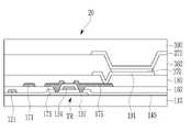
도 9를 참고하면, 디스플레이 패널(20)은 기판(110) 및 그 위에 형성된 여러 층들에 의해 형성되는 신호선들과 소자들을 포함한다. Referring to FIG. 9 , the
기판(110)은 고분자 필름으로 이루어진 연성 기판일 수 있다. 예컨대, 기판(110)은 폴리이미드(polyimide), 폴리아미드(polyamide), 폴리에틸렌 테레프탈레이드(polyethylene terephthalate) 등의 플라스틱으로 이루어질 수 있다. 기판(110)은 유리로 이루어진 경성 기판일 수도 있다.The
기판(110)은 반도체 특성을 열화시키는 불순물이 확산되는 것을 방지하고 수분 등의 침투를 방지하기 위한 배리어층(도시되지 않음)을 포함할 수 있다.The
기판(110) 위에는 트랜지스터(TR)의 반도체(131)가 위치하고, 반도체(131) 위에는 게이트 절연층(140)이 위치한다. 반도체(131)는 소스 영역, 드레인 영역 및 이들 영역 사이의 채널 영역을 포함한다. 반도체(131)는 다결정 규소, 산화물 반도체, 또는 비정질 규소를 포함할 수 있다. 게이트 절연층(140)은 규소 산화물, 규소 질화물 같은 무기 절연 물질을 적층(deposition)하여 형성될 수 있다.A
게이트선(121)과 트랜지스터(TR)의 게이트 전극(124)을 포함하는 게이트 도전체가 위치한다. 게이트 도전체는 기판(110) 위에 구리(Cu), 알루미늄(Al), 은(Ag), 몰리브덴(Mo), 크롬(Cr), 탄탈륨(Ta), 티타늄(Ti) 같은 도전성 물질을 적층하고 패터닝하여 함께 형성될 수 있다.A gate conductor including the
게이트 도전체로서 구리를 사용하는 경우, 기판(110) 위에 예컨대 스퍼터링 등을 통해 구리층을 형성한다. 그 후, 구리층 위에 마스크를 형성 또는 배치하고 전술한 실시예들에 따른 구리 플라즈마 식각 방법을 사용하여 구리층을 식각함으로써 패터닝된 구리층인 게이트 도전체를 형성할 수 있다. 구리층의 식각 시 기판(110)이 놓이는 서셉터의 온도를 약 10℃ 이하로 낮게 유지함으로써 기판(110)의 온도를 낮출 수 있고, 식각 가스에 추가되는 H2가 CuCl2와 흡열 반응하여 기판(110)의 온도를 낮출 수 있으므로, 고온에서 취약할 수 있는 포토레지스트를 마스크로서 사용할 수 있다. 또한, 기판(110)의 온도를 낮게 유지하므로, 예컨대 플라스틱 기판을 사용하더라도 구리층의 건식 식각 동안 기판(110)이 손상되지 않는다.When copper is used as the gate conductor, a copper layer is formed on the
게이트 도전체 위에는 층간 절연층(160)이 위치한다. 층간 절연층(160)은 무기 절연 물질을 포함할 수 있다. 층간 절연층(160) 위에는 데이터선(171)과 트랜지스터(TR)의 소스 전극(173) 및 드레인 전극(175)을 포함하는 데이터 도전체가 위치한다. 소스 전극(173) 및 드레인 전극(175)은 층간 절연층(160) 및 게이트 절연층(140)에 형성된 접촉 구멍들을 통해 반도체(131)의 소스 영역 및 드레인 전극과 각각 연결되어 있다. 데이터 도전체는 구리(Cu), 알루미늄(Al), 은(Ag), 몰리브덴(Mo), 크롬(Cr), 금(Au), 백금(Pt), 팔라듐(Pd), 탄탈륨(Ta), 텅스텐(W), 티타늄(Ti), 니켈(Ni) 등의 금속이나 금속 합금을 포함할 수 있다. 데이터 도전체로서 구리를 사용하는 경우, 전술한 게이트 도전체로서 구리를 사용하는 경우와 같은 방식으로 구리층을 식각하여 데이터 도전체를 형성할 수 있다.An interlayer insulating
소소 전극(173) 및 드레인 전극(175) 위에는 평탄화층(180)이 위치한다. 평탄화층(180)은 유기 절연 물질을 포함할 수 있고, 무기 절연 물질을 포함할 수도 있다.A
평탄화층(180) 위에는 화소 전극(191)이 위치한다. 화소 전극(191)은 평탄화층(180)에 형성된 접촉 구멍을 통해 드레인 전극(175)과 연결되어 데이터 신호를 인가받을 수 있다. 기판(110)으로부터 화소 전극(191)까지의 층들을 포함하는 부분을 트랜지스터 디스플레이 패널이라고 부를 수 있다. A
평탄화층(180)과 화소 전극(191)의 일부 위에는 화소 정의막(360)이 위치한다. 화소 정의막(360)은 화소 전극(191)과 중첩하는 개구부(opening)를 가진다. 화소 정의막(360)의 개구부에는 화소 전극(191) 위로 발광층(370)이 위치하고, 발광층(370) 위에는 공통 전극(270)이 위치한다. 화소 전극(191), 발광층(370) 및 공통 전극(270)은 함께 유기 발광 다이오드를 구성한다. 화소 전극(191)은 유기 발광 다이오드의 애노드(anode)일 수 있고, 공통 전극(270)은 유기 발광 다이오드의 캐소드(cathode)일 수 있다. 공통 전극(270)은 인듐 주석 산화물(ITO), 인듐 아연 산화물(IZO) 같은 투명한 도전 물질을 포함할 수 있다. 공통 전극(270)의 위에는 유기 발광 다이오드를 보호하는 봉지층(encapsulation layer)(390)이 위치한다.A
액정 디스플레이 패널(30)과 관련하여 도 10을 참고하면, 기판(110) 위에 게이트선(121) 및 트랜지스터(TR)의 게이트 전극(124)이 위치하고, 그 위로 게이트 절연층(140)이 위치한다. 게이트 절연층(140) 위에는 반도체(151) 및 트랜지스터(TR)의 반도체(154)가 위치하고, 반도체(151) 위에는 데이터선(171)이 위치하고, 반도체(154) 위에 트랜지스터(TR)의 소스 전극(173) 및 드레인 전극(175)이 위치한다.Referring to FIG. 10 in relation to the liquid
게이트선(121) 및 게이트 전극(124)을 포함하는 게이트 도전체를 구리로 형성하는 경우, 기판(110) 위에 구리층을 형성한 후 전술한 실시예들에 따른 구리 플라즈마 식각 방법을 사용하여 구리층을 식각함으로써 패터닝된 구리층인 게이트 도전체를 형성할 수 있다. 데이터선(171), 소스 전극(173) 및 드레인 전극(175)을 포함하는 데이터 도전체를 구리로 형성하는 경우, 기판(110) 위에 구리층을 형성한 후 전술한 실시예들에 따른 구리 플라즈마 식각 방법을 사용하여 구리층을 식각함으로써 패터닝된 구리층인 데이터 도전체를 형성할 수 있다.When the gate conductor including the
데이터 도전체 위에는 평탄화층(180)이 위치하고, 평탄화층(180) 위에는 화소 전극(191)이 위치한다. 화소 전극(191)은 평탄화층(180)에 형성된 접촉 구멍을 통해 드레인 전극(175)과 연결되어 데이터 신호를 인가받을 수 있다. 기판(110)으로부터 화소 전극(191)까지의 층들을 포함하는 부분을 트랜지스터 디스플레이 패널이라고 부를 수 있다.A
화소 전극(191) 위에는 액정 분자들(31)을 포함하는 액정층(3)이 위치하고, 액정층(3) 위에는 기판(110)과 함께 액정층(3)을 밀봉하는 절연층(210)이 위치한다. 절연층(210)은 기판 형태일 수 있다. 액정층(3)은 미세 공간들 내에 이격되게 위치하도록 형성될 수도 있다.A
절연층(210)의 아래에는 화소 전극(191)과 함께 액정층(3)에 전계를 생성하여 액정 분자들(31)의 배열 방향을 제어할 수 있는 공통 전극(270)이 위치한다. 화소 전극(191)과 액정층(3) 사이, 그리고 액정층(3)과 공통 전극(270) 사이에는 배향막(도시되지 않음)이 위치할 수 있다. 공통 전극(270)은 기판(110)과 액정층(3) 사이에 위치할 수도 있다.A
이상에서 본 발명의 실시예에 대하여 상세하게 설명하였지만 본 발명의 권리범위는 이에 한정되는 것은 아니고 다음의 청구범위에서 정의하고 있는 본 발명의 기본 개념을 이용한 당업자의 여러 변형 및 개량 형태 또한 본 발명의 권리범위에 속하는 것이다.Although the embodiments of the present invention have been described in detail above, the scope of the present invention is not limited thereto, and various modifications and improvements made by those skilled in the art using the basic concept of the present invention defined in the following claims are also included in the scope of the present invention. that fall within the scope of the right.
10: 플라즈마 식각 장치
20: 유기 발광 디스플레이 패널
30: 액정 디스플레이 패널10: plasma etching device
20: organic light emitting display panel
30: liquid crystal display panel
Claims (20)
Translated fromKorean상기 공정 챔버 내로 염화수소 및 H2 가스를 포함하는 식각 가스를 공급하는 단계,
상기 기판에서 구리를 포함하는 도전층을 플라즈마 식각하는 단계, 그리고
상기 플라즈마 식각하는 동안 상기 서셉터의 온도를 10℃ 미만으로 유지하는 단계
를 포함하며,
상기 염화수소에 대한 상기 H2 가스의 유량비가 0.5 이하이고,
상기 플라즈마 식각은 120초 내지 300초 동안 수행되는 구리 플라즈마 식각 방법.Placing a substrate on a susceptor in a process chamber of a plasma etching apparatus;
Supplying an etching gas containing hydrogen chloride and H2 gas into the process chamber;
Plasma etching a conductive layer containing copper on the substrate, and
Maintaining the temperature of the susceptor at less than 10° C. during the plasma etching
Including,
The flow rate ratio of the H2 gas to the hydrogen chloride is 0.5 or less,
The plasma etching method is performed for 120 seconds to 300 seconds.
상기 플라즈마 식각 단계에서 하기 반응 단계를 포함하는 구리 플라즈마 식각 방법:
1단계: Cu + Cl → CuCl(s)
2단계: CuCl + Cl → CuCl2(s)
3단계: CuCl2 + 3H → CuH(g) + 2HCl(g)
3CuCl2 + 3H → Cu3Cl3(g) + 3HCl(g)
3CuCl2 + 3/2H2 → Cu3Cl3(g) + 3HCl(g).In paragraph 1,
A copper plasma etching method comprising the following reaction steps in the plasma etching step:
Step 1: Cu + Cl → CuCl(s )
Step 2: CuCl + Cl → CuCl2 (s )
Step 3: CuCl2 + 3H → CuH (g ) + 2HCl (g )
3CuCl2 + 3H → Cu3 Cl3 (g ) + 3HCl (g )
3CuCl2 + 3/2H2 → Cu3 Cl3 (g ) + 3HCl (g ).
상기 플라즈마 식각 단계에서 수소 라디칼의 수가 염소 라디칼의 수와 동일하거나 그보다 많은 구리 플라즈마 식각 방법.In paragraph 1,
Copper plasma etching method in which the number of hydrogen radicals is equal to or greater than the number of chlorine radicals in the plasma etching step.
상기 플라즈마 식각 단계는 전자 사이클로트론 공명(ECR) 플라즈마 소스에 의해 형성된 플라즈마를 사용하여 수행되는 구리 플라즈마 식각 방법.In paragraph 1,
The plasma etching step is performed using a plasma formed by an electron cyclotron resonance (ECR) plasma source.
상기 플라즈마 식각 단계에서 반응성 이온 식각을 적용하는 구리 플라즈마 식각 방법.In paragraph 1,
Copper plasma etching method of applying reactive ion etching in the plasma etching step.
상기 플라즈마 식각 단계는 10-2 내지 10-4Torr의 공정 압력 하에서 수행되는 구리 플라즈마 식각 방법.In paragraph 1,
The plasma etching step is performed under a process pressure of 10-2 to 10-4 Torr.
상기 플라즈마 식각 단계에서 식각 마스크로서 포토레지스트 마스크를 사용하는 구리 플라즈마 식각 방법.In paragraph 1,
A copper plasma etching method using a photoresist mask as an etching mask in the plasma etching step.
상기 도전층이 형성된 기판을 플라즈마 식각 장치의 공정 챔버 내의 서셉터 위에 배치하는 단계,
상기 공정 챔버 내에 염화수소 및 H2 가스를 포함하는 식각 가스를 공급하는 단계,
상기 도전층을 플라즈마 식각하는 단계, 그리고
상기 플라즈마 식각하는 동안 상기 서셉터의 온도를 10℃ 미만으로 유지하는 단계
를 포함하며,
상기 염화수소에 대한 상기 H2 가스의 유량비가 0.5 이하이고,
상기 플라즈마 식각은 120초 내지 300초 동안 수행되는 디스플레이 패널 제조 방법.Forming a conductive layer containing copper on a substrate;
Disposing the substrate on which the conductive layer is formed on a susceptor in a process chamber of a plasma etching apparatus;
Supplying an etching gas containing hydrogen chloride and H2 gas into the process chamber;
Plasma etching the conductive layer, and
Maintaining the temperature of the susceptor at less than 10° C. during the plasma etching
Including,
The flow rate ratio of the H2 gas to the hydrogen chloride is 0.5 or less,
The plasma etching method of manufacturing a display panel is performed for 120 seconds to 300 seconds.
상기 플라즈마 식각 단계에서 하기 반응 단계를 포함하는 디스플레이 패널 제조 방법.
1단계: Cu + Cl → CuCl(s)
2단계: CuCl + Cl → CuCl2(s)
3단계: CuCl2 + 3H → CuH(g) + 2HCl(g)
3CuCl2 + 3H → Cu3Cl3(g) + 3HCl(g)
3CuCl2 + 3/2H2 → Cu3Cl3(g) + 3HCl(g).In paragraph 10,
Display panel manufacturing method comprising the following reaction step in the plasma etching step.
Step 1: Cu + Cl → CuCl(s )
Step 2: CuCl + Cl → CuCl2 (s )
Step 3: CuCl2 + 3H → CuH (g ) + 2HCl (g )
3CuCl2 + 3H → Cu3 Cl3 (g ) + 3HCl (g )
3CuCl2 + 3/2H2 → Cu3 Cl3 (g ) + 3HCl (g ).
상기 플라즈마 식각 단계에서 수소 라디칼의 수가 염소 라디칼의 수와 동일하거나 그보다 많은 디스플레이 패널 제조 방법.In paragraph 10,
A display panel manufacturing method in which the number of hydrogen radicals is equal to or greater than the number of chlorine radicals in the plasma etching step.
상기 플라즈마 식각 단계는 전자 사이클로트론 공명(ECR) 플라즈마 소스에 의해 형성된 플라즈마를 사용하여 수행되는 디스플레이 패널 제조 방법.In paragraph 10,
The plasma etching step is performed using plasma formed by an electron cyclotron resonance (ECR) plasma source.
상기 플라즈마 식각 단계에서 반응성 이온 식각을 적용하는 디스플레이 패널 제조 방법.In paragraph 10,
A display panel manufacturing method of applying reactive ion etching in the plasma etching step.
상기 도전층을 플라즈마 식각하는 단계는 게이트선 및 게이트 전극을 형성하는 단계를 포함하는 디스플레이 패널 제조 방법.In paragraph 10,
Plasma etching the conductive layer includes forming a gate line and a gate electrode.
상기 도전층을 플라즈마 식각하는 단계는 데이터선, 소스 전극 및 드레인 전극을 형성하는 단계를 포함하는 디스플레이 패널 제조 방법.In paragraph 10,
Plasma etching the conductive layer includes forming a data line, a source electrode, and a drain electrode.
상기 플라즈마 식각 단계는 10-2 내지 10-4Torr의 공정 압력 하에서 수행되는 디스플레이 패널 제조 방법.In paragraph 10,
The plasma etching step is performed under a process pressure of 10-2 to 10-4 Torr.
상기 기판은 플라스틱 기판인 디스플레이 패널 제조 방법.In paragraph 10,
The substrate is a display panel manufacturing method of a plastic substrate.
Priority Applications (3)
| Application Number | Priority Date | Filing Date | Title |
|---|---|---|---|
| KR1020170127794AKR102492733B1 (en) | 2017-09-29 | 2017-09-29 | Copper plasma etching method and manufacturing method of display panel |
| US16/106,739US10910232B2 (en) | 2017-09-29 | 2018-08-21 | Copper plasma etching method and manufacturing method of display panel |
| CN201811011271.1ACN109599331B (en) | 2017-09-29 | 2018-08-31 | Copper plasma etching method and manufacturing method of display panel |
Applications Claiming Priority (1)
| Application Number | Priority Date | Filing Date | Title |
|---|---|---|---|
| KR1020170127794AKR102492733B1 (en) | 2017-09-29 | 2017-09-29 | Copper plasma etching method and manufacturing method of display panel |
Publications (3)
| Publication Number | Publication Date |
|---|---|
| KR20190038709A KR20190038709A (en) | 2019-04-09 |
| KR102492733B1true KR102492733B1 (en) | 2023-01-27 |
| KR102492733B9 KR102492733B9 (en) | 2024-02-08 |
Family
ID=65898004
Family Applications (1)
| Application Number | Title | Priority Date | Filing Date |
|---|---|---|---|
| KR1020170127794AActiveKR102492733B1 (en) | 2017-09-29 | 2017-09-29 | Copper plasma etching method and manufacturing method of display panel |
Country Status (3)
| Country | Link |
|---|---|
| US (1) | US10910232B2 (en) |
| KR (1) | KR102492733B1 (en) |
| CN (1) | CN109599331B (en) |
Cited By (1)
| Publication number | Priority date | Publication date | Assignee | Title |
|---|---|---|---|---|
| KR102871339B1 (en) | 2023-12-15 | 2025-10-15 | 주식회사 라이트브릿지 | Stack electrode manufacturing method using hydrogen reduction plasma and electrode manufactured thereby |
Families Citing this family (5)
| Publication number | Priority date | Publication date | Assignee | Title |
|---|---|---|---|---|
| KR102619877B1 (en)* | 2019-09-11 | 2024-01-03 | 삼성전자주식회사 | Substrate treatment apparatus |
| KR102837276B1 (en) | 2021-03-30 | 2025-07-23 | 삼성디스플레이 주식회사 | Display device and method of manufacturing of the display device |
| US11557487B2 (en)* | 2021-06-04 | 2023-01-17 | Tokyo Electron Limited | Etching metal during processing of a semiconductor structure |
| CN119451511A (en) | 2023-08-04 | 2025-02-14 | 东京毅力科创株式会社 | Copper layer etching method and substrate processing device |
| WO2025071164A1 (en)* | 2023-09-26 | 2025-04-03 | 에이피에스리서치 주식회사 | Method for dry etching copper thin film |
Citations (5)
| Publication number | Priority date | Publication date | Assignee | Title |
|---|---|---|---|---|
| US20060014394A1 (en)* | 2001-10-31 | 2006-01-19 | Kulkarni Nagraj S | Process for low temperature, dry etching, and dry planarization of copper |
| JP2007520059A (en)* | 2003-12-22 | 2007-07-19 | ラム リサーチ コーポレーション | Substrate processing method, plasma chamber and semiconductor device |
| US20090014324A1 (en)* | 2006-10-26 | 2009-01-15 | Mark Naoshi Kawaguchi | Integrated apparatus for efficient removal of halogen residues from etched substrates |
| US20130037793A1 (en)* | 2011-08-11 | 2013-02-14 | Qualcomm Mems Technologies, Inc. | Amorphous oxide semiconductor thin film transistor fabrication method |
| US20150099369A1 (en)* | 2013-10-03 | 2015-04-09 | Applied Materials, Inc. | Process for etching metal using a combination of plasma and solid state sources |
Family Cites Families (200)
| Publication number | Priority date | Publication date | Assignee | Title |
|---|---|---|---|---|
| JPH0621004A (en) | 1991-04-22 | 1994-01-28 | Nec Corp | Plasma etching device |
| JP2793472B2 (en) | 1993-06-24 | 1998-09-03 | 日本電気株式会社 | Copper fine processing method and copper fine processing apparatus |
| US5736002A (en)* | 1994-08-22 | 1998-04-07 | Sharp Microelectronics Technology, Inc. | Methods and equipment for anisotropic, patterned conversion of copper into selectively removable compounds and for removal of same |
| JPH08111420A (en)* | 1994-10-12 | 1996-04-30 | Fujitsu Ltd | Method and apparatus for manufacturing semiconductor device |
| US6342733B1 (en) | 1999-07-27 | 2002-01-29 | International Business Machines Corporation | Reduced electromigration and stressed induced migration of Cu wires by surface coating |
| JP2001291720A (en) | 2000-04-05 | 2001-10-19 | Hitachi Ltd | Semiconductor integrated circuit device and method of manufacturing semiconductor integrated circuit device |
| JP3914452B2 (en) | 2001-08-07 | 2007-05-16 | 株式会社ルネサステクノロジ | Manufacturing method of semiconductor integrated circuit device |
| KR20040033619A (en) | 2002-10-15 | 2004-04-28 | 주식회사 하이닉스반도체 | Method for forming capacitor in semiconductor device |
| WO2004097943A1 (en) | 2003-04-28 | 2004-11-11 | Matsushita Electric Industrial Co., Ltd. | Semiconductor device and method for manufacturing same |
| US20060289203A1 (en) | 2003-05-19 | 2006-12-28 | Dai Nippon Printing Co., Ltd. | Double-sided wiring board, double sided wiring board manufacturing method, and multilayer wiring board |
| US20050274396A1 (en) | 2004-06-09 | 2005-12-15 | Hong Shih | Methods for wet cleaning quartz surfaces of components for plasma processing chambers |
| JP2006038999A (en) | 2004-07-23 | 2006-02-09 | Sumitomo Electric Ind Ltd | Method for forming conductive circuit using laser irradiation and conductive circuit |
| US20080135868A1 (en) | 2004-10-01 | 2008-06-12 | Mitsubishi Cable Industries, Ltd. | Nitride Semiconductor Light Emitting Element and Method for Manufacturing the Same |
| US20060084271A1 (en) | 2004-10-20 | 2006-04-20 | Yang Andy C | Systems, methods and slurries for chemical mechanical polishing |
| JP2006154722A (en) | 2004-10-28 | 2006-06-15 | Daikin Ind Ltd | Stripping solution and stripping method for ashing residue of Cu / low-k multilayer wiring structure |
| KR100856281B1 (en) | 2004-11-24 | 2008-09-03 | 삼성전기주식회사 | Semiconductor laser diode and manufacturing method thereof |
| US20060124956A1 (en) | 2004-12-13 | 2006-06-15 | Hui Peng | Quasi group III-nitride substrates and methods of mass production of the same |
| TWI252559B (en) | 2004-12-31 | 2006-04-01 | Ind Tech Res Inst | Method for connecting magnetoelectronic element with conductive line |
| US20060154393A1 (en) | 2005-01-11 | 2006-07-13 | Doan Trung T | Systems and methods for removing operating heat from a light emitting diode |
| US20060234499A1 (en) | 2005-03-29 | 2006-10-19 | Akira Kodera | Substrate processing method and substrate processing apparatus |
| TWI248877B (en) | 2005-04-25 | 2006-02-11 | Benq Corp | Method for fabricating a monolithic fluid eject device |
| JP2007004775A (en) | 2005-05-23 | 2007-01-11 | Toshiba Corp | Semiconductor memory card |
| US20060270229A1 (en) | 2005-05-27 | 2006-11-30 | General Electric Company | Anodized aluminum oxide nanoporous template and associated method of fabrication |
| KR20060131071A (en) | 2005-06-15 | 2006-12-20 | 삼성전자주식회사 | Wiring for a display device, a thin film transistor array panel comprising the same, and a manufacturing method thereof |
| KR100723489B1 (en) | 2005-06-17 | 2007-05-31 | 삼성전자주식회사 | Semiconductor device capable of improving reliability and manufacturing method thereof |
| US20070004066A1 (en) | 2005-07-01 | 2007-01-04 | Dong-Sing Wuu | Method for manufacturing a light emitting device and a light emitting device manufactured therefrom |
| JP5096669B2 (en) | 2005-07-06 | 2012-12-12 | ルネサスエレクトロニクス株式会社 | Manufacturing method of semiconductor integrated circuit device |
| KR20070014579A (en) | 2005-07-29 | 2007-02-01 | 삼성전자주식회사 | Organic thin film transistor array panel and manufacturing method thereof |
| DE102005039323B4 (en) | 2005-08-19 | 2009-09-03 | Infineon Technologies Ag | Guideway arrangement and associated production method |
| US20070108063A1 (en) | 2005-09-28 | 2007-05-17 | Ebara Corporation | Layer forming method, layer forming apparatus, workpiece processing apparatus, interconnect forming method, and substrate interconnect structure |
| WO2007043718A1 (en) | 2005-10-11 | 2007-04-19 | Tae-Seok Park | Wafer level package using silicon via contacts for cmos image sensor and method of fabricating the same |
| US20070082475A1 (en) | 2005-10-12 | 2007-04-12 | Dongbu Electronics Co., Ltd. | Method for forming bonding pad and semiconductor device having the bonding pad formed thereby |
| JP4855758B2 (en) | 2005-10-19 | 2012-01-18 | 東海旅客鉄道株式会社 | Method for producing diamond having acicular protrusion arrangement structure on surface |
| JP2007123721A (en) | 2005-10-31 | 2007-05-17 | Rohm Co Ltd | Method for manufacturing photoelectric conversion device and photoelectric conversion device |
| DK1948850T3 (en) | 2005-11-18 | 2019-07-29 | Luxembourg Inst Science & Tech List | PROCEDURE FOR MAKING A MULTIPLE LAYER STRUCTURE |
| EP1798800A1 (en) | 2005-12-14 | 2007-06-20 | Ecole Polytechnique Fédérale de Lausanne (EPFL) | Metallic supporting grid for ultrathin electrolyte membranes in solid oxide fuel cells |
| US20070158632A1 (en) | 2006-01-09 | 2007-07-12 | Macronix International Co., Ltd. | Method for Fabricating a Pillar-Shaped Phase Change Memory Element |
| DE102006008261A1 (en) | 2006-02-22 | 2007-08-30 | Fraunhofer-Gesellschaft zur Förderung der angewandten Forschung e.V. | Etching solution for etching layer system, comprising phosphoric acid, nitric acid, de-ionized water and halogen component, which releases halogen ions that contain these components |
| US20070224359A1 (en) | 2006-03-22 | 2007-09-27 | Burin David L | Method for preparing strain tolerant coatings by a sol-gel process |
| KR100764360B1 (en) | 2006-04-28 | 2007-10-08 | 주식회사 하이닉스반도체 | Semiconductor device and manufacturing method thereof |
| US20070277866A1 (en) | 2006-05-31 | 2007-12-06 | General Electric Company | Thermoelectric nanotube arrays |
| US20080124924A1 (en) | 2006-07-18 | 2008-05-29 | Applied Materials, Inc. | Scheme for copper filling in vias and trenches |
| TWI351085B (en) | 2006-08-08 | 2011-10-21 | Silicon Base Dev Inc | Structure and manufacturing method of package base for power semiconductor device |
| KR100831405B1 (en) | 2006-10-02 | 2008-05-21 | (주) 파이오닉스 | Wafer Bonding Packaging Method |
| JP2010507909A (en) | 2006-10-19 | 2010-03-11 | ソロパワー、インコーポレイテッド | Roll-to-roll electroplating for the production of photovoltaic films |
| KR20080037296A (en) | 2006-10-25 | 2008-04-30 | 삼성전자주식회사 | Thin film transistor substrate and manufacturing method thereof |
| DE102007050843A1 (en) | 2006-10-26 | 2008-05-21 | Samsung Electronics Co., Ltd., Suwon | Integrated circuit manufacturing method, involves forming hole via intermediate layer to expose buffer layer section, removing exposed section to expose catalyst layer section, and waxing carbon-nano tubes at catalyst layer exposed section |
| TW200822788A (en) | 2006-11-09 | 2008-05-16 | Univ Nat Central | Method of using laser in fabricating GaN device |
| US20080142941A1 (en) | 2006-12-19 | 2008-06-19 | Advanced Chip Engineering Technology Inc. | 3d electronic packaging structure with enhanced grounding performance and embedded antenna |
| US20080206562A1 (en) | 2007-01-12 | 2008-08-28 | The Regents Of The University Of California | Methods of generating supported nanocatalysts and compositions thereof |
| KR20080073019A (en) | 2007-02-05 | 2008-08-08 | 삼성전자주식회사 | Nano or micro sized organic-inorganic composite device and its manufacturing method |
| US20080203571A1 (en) | 2007-02-28 | 2008-08-28 | Gotthard Jungnickel | Backside metallization for integrated circuit devices |
| US20080217775A1 (en) | 2007-03-07 | 2008-09-11 | Taiwan Semiconductor Manufacturing Co., Ltd. | Method of forming contact plugs for eliminating tungsten seam issue |
| TWI331371B (en) | 2007-04-19 | 2010-10-01 | Siliconware Precision Industries Co Ltd | Semiconductor device and manufacturing method thereof |
| US20080277678A1 (en) | 2007-05-08 | 2008-11-13 | Huga Optotech Inc. | Light emitting device and method for making the same |
| KR100871768B1 (en) | 2007-05-18 | 2008-12-05 | 주식회사 동부하이텍 | Semiconductor element and COA / COA manufacturing method |
| US10096789B2 (en) | 2007-05-23 | 2018-10-09 | University Of Florida Research Foundation, Inc. | Method and apparatus for light absorption and charged carrier transport |
| KR100891401B1 (en) | 2007-06-28 | 2009-04-02 | 주식회사 하이닉스반도체 | Chemical Mechanical Polishing Method of Semiconductor Devices |
| US20090008777A1 (en) | 2007-07-06 | 2009-01-08 | Advanced Chip Engineering Technology Inc. | Inter-connecting structure for semiconductor device package and method of the same |
| KR100884987B1 (en) | 2007-08-27 | 2009-02-23 | 주식회사 동부하이텍 | Copper wiring formation method of semiconductor device |
| WO2009050207A1 (en) | 2007-10-15 | 2009-04-23 | Interuniversitair Microelectronica Centrum Vzw | Method for producing electrical interconnects and devices made thereof |
| US20090102052A1 (en) | 2007-10-22 | 2009-04-23 | Sang Wook Ryu | Semiconductor Device and Fabricating Method Thereof |
| KR100902862B1 (en) | 2007-11-07 | 2009-06-16 | (주)탑나노시스 | Transparent electronic board and manufacturing method thereof |
| US20090159976A1 (en) | 2007-12-20 | 2009-06-25 | Matthias Goldbach | Integrated circuit and method for making an integrated circuit |
| US20090166873A1 (en) | 2007-12-27 | 2009-07-02 | Advanced Chip Engineering Technology Inc. | Inter-connecting structure for semiconductor device package and method of the same |
| US20090170305A1 (en) | 2007-12-31 | 2009-07-02 | Texas Instruments Incorporated | Method for improving electromigration lifetime for cu interconnect systems |
| CN104076600B (en) | 2008-01-25 | 2019-02-15 | 旭化成株式会社 | Method for manufacturing seamless mold |
| KR100966336B1 (en) | 2008-04-07 | 2010-06-28 | 삼성전기주식회사 | High Density Circuit Board and Formation Method |
| DE102008022793B4 (en) | 2008-05-08 | 2010-12-16 | Universität Ulm | Fully self-aligned surface-emitting surface-mount semiconductor laser with optimized properties |
| US20110089141A1 (en) | 2008-06-17 | 2011-04-21 | Ulvac,Inc. | Method for the production of multi-stepped substrate |
| KR20100019233A (en) | 2008-08-08 | 2010-02-18 | 삼성전자주식회사 | Thin film transistor substrate and method of fabricating the same |
| JP4638530B2 (en) | 2008-08-19 | 2011-02-23 | 日本電波工業株式会社 | Piezoelectric component and manufacturing method thereof |
| JP2010080897A (en) | 2008-09-29 | 2010-04-08 | Panasonic Corp | Semiconductor device and method for manufacturing the same |
| US20100120242A1 (en) | 2008-11-07 | 2010-05-13 | Texas Instruments Incorporated | Method to prevent localized electrical open cu leads in vlsi cu interconnects |
| TWI366890B (en) | 2008-12-31 | 2012-06-21 | Ind Tech Res Inst | Method of manufacturing through-silicon-via and through-silicon-via structure |
| US20100171173A1 (en) | 2009-01-08 | 2010-07-08 | Force Mos Technology Co. Ltd. | Trench mosfet with improved source-body contact |
| US20100200912A1 (en) | 2009-02-11 | 2010-08-12 | Force Mos Technology Co. Ltd. | Mosfets with terrace irench gate and improved source-body contact |
| KR20100104378A (en) | 2009-03-17 | 2010-09-29 | 삼성전자주식회사 | Electrode for supercapacitor, supercapacitor comprising the same, and method for preparing the electrode |
| KR20100117937A (en) | 2009-04-27 | 2010-11-04 | 삼성전자주식회사 | Thin film transistor substrate and method of fabricating the same |
| US20100291475A1 (en) | 2009-05-12 | 2010-11-18 | Chenghong Li | Silicone Coating Compositions |
| JPWO2011027745A1 (en) | 2009-09-01 | 2013-02-04 | ローム株式会社 | Photoelectric conversion device and method for manufacturing photoelectric conversion device |
| KR20110048338A (en) | 2009-11-02 | 2011-05-11 | 삼성전기주식회사 | Package board for optical element and manufacturing method thereof |
| TW201118059A (en) | 2009-11-20 | 2011-06-01 | Holy Stone Entpr Co Ltd | Manufacturing process for high precision ceramic substrate |
| TW201119535A (en) | 2009-11-20 | 2011-06-01 | Holy Stone Entpr Co Ltd | Ceramic substrate manufacturing method |
| TW201118940A (en) | 2009-11-20 | 2011-06-01 | Holy Stone Entpr Co Ltd | Ceramic substrate manufacturing method |
| CN101777514B (en) | 2010-02-03 | 2012-12-05 | 香港商莫斯飞特半导体有限公司 | A trench type semiconductor power device and its preparation method |
| US20110256658A1 (en) | 2010-02-05 | 2011-10-20 | Hitachi Chemical Company, Ltd. | Method for producing photovoltaic cell |
| US20130026462A1 (en) | 2010-03-04 | 2013-01-31 | Sharp Kabushiki Kaisha | Method for manufacturing thin film transistor and thin film transistor manufactured by the same, and active matrix substrate |
| US20110272287A1 (en) | 2010-05-07 | 2011-11-10 | International Business Machines Corporation | Method for patterning magnetic films |
| KR20110132136A (en) | 2010-06-01 | 2011-12-07 | 삼성전자주식회사 | Light emitting device using connection structure and manufacturing method thereof |
| US9018758B2 (en) | 2010-06-02 | 2015-04-28 | Taiwan Semiconductor Manufacturing Company, Ltd. | Cu pillar bump with non-metal sidewall spacer and metal top cap |
| US20120037983A1 (en) | 2010-08-10 | 2012-02-16 | Force Mos Technology Co., Ltd. | Trench mosfet with integrated schottky rectifier in same cell |
| US20120037935A1 (en) | 2010-08-13 | 2012-02-16 | Wen-Kun Yang | Substrate Structure of LED (light emitting diode) Packaging and Method of the same |
| KR20120017244A (en) | 2010-08-18 | 2012-02-28 | 삼성전기주식회사 | Multi-layer conductor line formation method and electronic paper panel using the same |
| KR20130092570A (en) | 2010-08-31 | 2013-08-20 | 도쿄엘렉트론가부시키가이샤 | Method for manufacturing semiconductor device |
| KR101661768B1 (en) | 2010-09-03 | 2016-09-30 | 엘지전자 주식회사 | Solar cell and manufacturing method thereof |
| KR101118929B1 (en) | 2010-09-13 | 2012-02-27 | 주성엔지니어링(주) | Manufacturing apparatus and manufacturing method of thin film solar cell |
| US20120098124A1 (en) | 2010-10-21 | 2012-04-26 | Taiwan Semiconductor Manufacturing Company, Ltd. | Semiconductor device having under-bump metallization (ubm) structure and method of forming the same |
| KR101204191B1 (en) | 2010-11-02 | 2012-11-23 | 삼성전기주식회사 | Heat-dissipating substrate |
| US9240328B2 (en) | 2010-11-19 | 2016-01-19 | Alphabet Energy, Inc. | Arrays of long nanostructures in semiconductor materials and methods thereof |
| US20120132529A1 (en) | 2010-11-30 | 2012-05-31 | Katholieke Universiteit Leuven, K.U.Leuven R&D | Method for precisely controlled masked anodization |
| EP2648205A2 (en) | 2010-12-01 | 2013-10-09 | SN Display Co., Ltd. | Field emission display device and manufacturing method thereof |
| CN102544246A (en) | 2010-12-20 | 2012-07-04 | 展晶科技(深圳)有限公司 | Method for manufacturing light emitting diode (LED) grains |
| WO2012088085A1 (en) | 2010-12-21 | 2012-06-28 | Alphabet Energy, Inc. | Arrays of filled nanostructures with protruding segments and methods thereof |
| KR101332422B1 (en) | 2011-01-07 | 2013-12-02 | 건국대학교 산학협력단 | Templated electrochemical growth of single-crystal Cu2O nanowire arrays |
| US20130014813A1 (en) | 2011-01-11 | 2013-01-17 | Weiming Wang | HIGH EFFICIENCY AND LOW COST GaInP/GaAs/Si TRIPLE JUNCTION BY EPITAXY LIFT-OFF AND MECHANICAL STACK |
| KR101188344B1 (en) | 2011-01-14 | 2012-10-05 | 광주과학기술원 | An optical fiber and coreless optical fiber having a cladding layer doped with metal nano particles, and manufacturing method of the same |
| KR101842018B1 (en) | 2011-04-01 | 2018-03-26 | 한화테크윈 주식회사 | Method for manufacturing film comprising graphene |
| US9082956B2 (en) | 2011-04-04 | 2015-07-14 | Micron Technology, Inc. | Confined cell structures and methods of forming confined cell structures |
| US9824892B2 (en) | 2011-05-17 | 2017-11-21 | Mcmaster University | Semiconductor formation by lateral diffusion liquid phase epitaxy |
| US20120305966A1 (en) | 2011-05-31 | 2012-12-06 | Electronics And Telecommunications Research Institute | Organic light emitting diode and method of fabricating the same |
| TWI446583B (en) | 2011-06-29 | 2014-07-21 | Univ Nat Chiao Tung | Semiconductor process method |
| KR20130003873A (en) | 2011-07-01 | 2013-01-09 | 삼성전자주식회사 | Paste, method of preparing same, and electronic device |
| US20130052475A1 (en) | 2011-08-23 | 2013-02-28 | Korea Institute Of Science And Technology | Method of fabricating porous film structure using dry processes and porous film structures fabricated by the same |
| US8686433B2 (en) | 2011-09-01 | 2014-04-01 | Rohm Co., Ltd. | Light emitting device and light emitting device package |
| KR101204564B1 (en) | 2011-09-30 | 2012-11-23 | 삼성전기주식회사 | Power Module Package And Method of Manufacturing The Same |
| US9593053B1 (en) | 2011-11-14 | 2017-03-14 | Hypersolar, Inc. | Photoelectrosynthetically active heterostructures |
| EP2785896B1 (en) | 2011-12-02 | 2015-09-23 | Altana AG | Method for producing electrically conductive structures on non-conductive substrates and structures made in this manner |
| CN103187323A (en) | 2011-12-28 | 2013-07-03 | 北大方正集团有限公司 | Semiconductor chip and thickening manufacture method of pressure welding block metal layer of semiconductor chip |
| EP2808735B1 (en) | 2012-01-27 | 2017-03-22 | Asahi Kasei Kabushiki Kaisha | Fine concavo-convex structure product, mold fabrication method, and use of a heat-reactive resist material |
| WO2013113328A1 (en) | 2012-02-02 | 2013-08-08 | Max-Planck-Gesellschaft zur Förderung der Wissenschaften e. V. | A method for preparing polystyrene-stabilized nanoparticles and nanostructured substrate surfaces comprising the same as well as the nanostructured substrate surfaces as such and uses thereof |
| KR101531082B1 (en) | 2012-03-12 | 2015-07-06 | 삼성전기주식회사 | Common mode filter and method of manufacturing the same |
| CN103305909B (en) | 2012-03-14 | 2016-01-20 | 东莞市中镓半导体科技有限公司 | A kind of preparation method of the compound substrate for GaN growth |
| US8629512B2 (en) | 2012-03-28 | 2014-01-14 | Taiwan Semiconductor Manufacturing Company, Ltd. | Gate stack of fin field effect transistor with slanted sidewalls |
| CN104137307B (en) | 2012-04-16 | 2017-09-22 | 株式会社Lg 化学 | The electrode for manufacturing the method for electrode of lithium secondary cell and being manufactured using it |
| DE102012008175A1 (en) | 2012-04-26 | 2013-10-31 | Heraeus Quarzglas Gmbh & Co. Kg | Process for producing a SiO 2 granulate |
| TWI464643B (en) | 2012-05-25 | 2014-12-11 | J Touch Corp | Method for manufacturing touch-sensitive element on polarizer and polarization device |
| JP2014005538A (en) | 2012-06-26 | 2014-01-16 | Samsung Corning Precision Materials Co Ltd | Zinc oxide-based sputtering target, method of manufacturing the same, and thin film transistor having shield film evaporated through the same |
| US20140014942A1 (en) | 2012-07-12 | 2014-01-16 | Polymer Vision B.V. | Thin-film transistor, electronic circuit, display and method of manufacturing the same |
| JP2014022657A (en) | 2012-07-20 | 2014-02-03 | Fujifilm Corp | Etching method, semiconductor substrate product and semiconductor element manufacturing method using the same, and etchant preparation kit |
| US20140027163A1 (en) | 2012-07-30 | 2014-01-30 | Samsung Electro-Mechanics Co., Ltd. | Printed circuit board and method for manufacturing the same |
| JP2014032999A (en) | 2012-08-01 | 2014-02-20 | Panasonic Liquid Crystal Display Co Ltd | Thin film transistor and manufacturing method thereof |
| JP6063206B2 (en) | 2012-10-22 | 2017-01-18 | 富士フイルム株式会社 | Etching solution, etching method using the same, and semiconductor device manufacturing method |
| JP2014086500A (en) | 2012-10-22 | 2014-05-12 | Tokyo Electron Ltd | Method of etching copper layer, and mask |
| EP2916334A1 (en) | 2012-10-30 | 2015-09-09 | Leap Co. Ltd. | Coil element production method |
| US20140151095A1 (en) | 2012-12-05 | 2014-06-05 | Samsung Electro-Mechanics Co., Ltd. | Printed circuit board and method for manufacturing the same |
| US20140175655A1 (en) | 2012-12-22 | 2014-06-26 | Industrial Technology Research Institute | Chip bonding structure and manufacturing method thereof |
| KR20140085023A (en) | 2012-12-27 | 2014-07-07 | 삼성전기주식회사 | Printed circuit board and method for manufacturing the same |
| KR20140086531A (en) | 2012-12-28 | 2014-07-08 | 삼성전기주식회사 | Package structure and manufacturing method thereof, and package on package substrate |
| KR101716468B1 (en) | 2013-01-11 | 2017-03-16 | 서울대학교산학협력단 | Tranfering method for graphene using self-adhesive film |
| WO2014159144A1 (en) | 2013-03-13 | 2014-10-02 | Applied Materials, Inc | Uv-assisted reactive ion etch for copper |
| WO2014150482A1 (en) | 2013-03-15 | 2014-09-25 | United Technologies Corporation | Bimetallic zincating processing for enhanced adhesion of aluminum on aluminum alloys |
| US20140291753A1 (en) | 2013-03-27 | 2014-10-02 | Force Mos Technology Co., Ltd. | Trench mosfet structure having self-aligned features for mask saving and on-resistance reduction |
| KR101427204B1 (en) | 2013-03-29 | 2014-08-08 | 케이조인스(주) | METHOD OF PERSISTENT CURRENT MODE SPLICING OF 2G ReBCO HIGH TEMPERATURE SUPERCONDUCTORS USING SOLID STATE PRESSURIZED ATOMS DIFFUSION BY DIRECT FACE-TO FACE CONTACT OF HIGH TEMPERATURE SUPERCONDUCTING LAYERS AND RECOVERING SUPERCONDUCTIVITY BY OXYGENATION ANNEALING |
| KR102089314B1 (en) | 2013-05-14 | 2020-04-14 | 엘지디스플레이 주식회사 | Oxide thin film transistor and method of fabricating the same |
| KR20140134420A (en) | 2013-05-14 | 2014-11-24 | 삼성전자주식회사 | Method for manufacturing semiconductor light emitting device package |
| KR101371185B1 (en) | 2013-05-21 | 2014-03-07 | 주식회사 화진 | Method for manufacturing a decoration element and a decoration element |
| US9893088B2 (en) | 2013-05-29 | 2018-02-13 | Joled Inc. | Thin film transistor device, method for manufacturing same and display device |
| FR3007041B1 (en) | 2013-06-17 | 2016-12-09 | Constellium Singen Gmbh | SHEET OR BAND FOR DECORATIVE CAR ROLLER FOR MOTOR VEHICLE |
| US9070687B2 (en) | 2013-06-28 | 2015-06-30 | Taiwan Semiconductor Manufacturing Co., Ltd. | Semiconductor device with self-protecting fuse |
| CN104284550A (en) | 2013-07-09 | 2015-01-14 | 三星电机株式会社 | High frequency module and manufacturing method thereof |
| US20150017482A1 (en) | 2013-07-09 | 2015-01-15 | Seagate Technology Llc | Method for fabricating plasmonic cladding |
| WO2015005154A1 (en) | 2013-07-09 | 2015-01-15 | Canon Kabushiki Kaisha | Liquid ejection head and process for producing the same |
| US9728777B2 (en) | 2013-07-26 | 2017-08-08 | Nanoteck Instruments, Inc. | Methods for mass-producing silicon nano powder and graphene-doped silicon nano powder |
| DE102013216848A1 (en) | 2013-08-23 | 2015-02-26 | Fraunhofer-Gesellschaft zur Förderung der angewandten Forschung e.V. | Long-term stable photovoltaic elements that can be deposited from solutions and in-situ processes for their production |
| WO2015029286A1 (en) | 2013-08-27 | 2015-03-05 | パナソニック株式会社 | Thin film transistor substrate manufacturing method and thin film transistor substrate |
| JP6434029B2 (en) | 2013-09-06 | 2018-12-05 | ソルベイ スペシャルティ ポリマーズ イタリー エス.ピー.エー. | Conductive assembly |
| JP6044719B2 (en) | 2013-09-09 | 2016-12-14 | 株式会社村田製作所 | Piezoelectric thin film element and manufacturing method thereof |
| US10510576B2 (en) | 2013-10-14 | 2019-12-17 | Corning Incorporated | Carrier-bonding methods and articles for semiconductor and interposer processing |
| US9354390B2 (en) | 2013-12-11 | 2016-05-31 | Taiwan Semiconductor Manufacturing Company, Ltd. | Semiconductor device and method of manufacturing |
| DE102013114496A1 (en) | 2013-12-19 | 2015-06-25 | Bundesdruckerei Gmbh | Zinc sulfide phosphor with photo and electroluminescent behavior, process for its preparation and security document, security feature and method for its detection |
| CN106165111A (en) | 2014-01-15 | 2016-11-23 | 密歇根大学董事会 | Integration of epitaxial exfoliated solar cells with mini-parabolic concentrator arrays via printing method |
| US9919921B2 (en) | 2014-01-24 | 2018-03-20 | The Regents Of The University Of Colorado, A Body Corporate | Methods of preparing nanodevices |
| US10258975B2 (en) | 2014-01-29 | 2019-04-16 | Indian Institute Of Technology Kanpur | Polymeric nanocomposite films with embedded channels and methods for their preparation and use |
| EP3119924A4 (en) | 2014-03-18 | 2017-11-29 | FUJIFILM Electronic Materials U.S.A, Inc. | Etching composition |
| US9318439B2 (en) | 2014-03-21 | 2016-04-19 | Taiwan Semiconductor Manufacturing Company Ltd. | Interconnect structure and manufacturing method thereof |
| US10141465B2 (en) | 2014-04-04 | 2018-11-27 | The Regents Of The University Of Michigan | Epitaxial lift-off processed GaAs thin-film solar cells integrated with non-tracking mini-compound parabolic concentrators |
| IN2014DE01015A (en) | 2014-04-10 | 2015-10-16 | Indian Inst Technology Kanpur | |
| US20150340422A1 (en) | 2014-05-23 | 2015-11-26 | Texas Instruments Incorporated | Method of manufacturing a micro-fabricated wafer level integrated inductor or transformer for high frequency switch mode power supplies |
| CN104037066B (en) | 2014-06-25 | 2017-05-31 | 深圳市华星光电技术有限公司 | The method for defining polycrystalline silicon growth direction |
| US10147613B2 (en) | 2014-06-30 | 2018-12-04 | Tokyo Electron Limited | Neutral beam etching of Cu-containing layers in an organic compound gas environment |
| CN104078424B (en) | 2014-06-30 | 2017-02-15 | 京东方科技集团股份有限公司 | Low-temperature poly-silicon TFT array substrate, manufacturing method thereof and display device |
| WO2016013649A1 (en) | 2014-07-25 | 2016-01-28 | 株式会社村田製作所 | Electronic component and method for producing same |
| US9279192B2 (en) | 2014-07-29 | 2016-03-08 | Dow Corning Corporation | Method for manufacturing SiC wafer fit for integration with power device manufacturing technology |
| US9999870B2 (en) | 2014-09-12 | 2018-06-19 | Paul Gregory O'BRIEN | Nanostructured solar selective catalytic supports |
| CN105513964B (en) | 2014-09-24 | 2019-12-31 | 中芯国际集成电路制造(上海)有限公司 | How the transistor is formed |
| US9570320B2 (en)* | 2014-10-09 | 2017-02-14 | Lam Research Corporation | Method to etch copper barrier film |
| CN105575887B (en) | 2014-10-16 | 2018-10-16 | 中芯国际集成电路制造(上海)有限公司 | The forming method of interconnection structure |
| CN105575946A (en) | 2014-10-16 | 2016-05-11 | 中芯国际集成电路制造(上海)有限公司 | Semiconductor structure and formation method thereof |
| KR102299875B1 (en) | 2014-11-07 | 2021-09-07 | 엘지디스플레이 주식회사 | Touch panel, method of manufacturing the same and touch panel integrated organic light emitting display device |
| US9899546B2 (en) | 2014-12-05 | 2018-02-20 | Tesla, Inc. | Photovoltaic cells with electrodes adapted to house conductive paste |
| US10020300B2 (en) | 2014-12-18 | 2018-07-10 | Agilome, Inc. | Graphene FET devices, systems, and methods of using the same for sequencing nucleic acids |
| US9859394B2 (en) | 2014-12-18 | 2018-01-02 | Agilome, Inc. | Graphene FET devices, systems, and methods of using the same for sequencing nucleic acids |
| KR101681242B1 (en) | 2015-01-19 | 2016-11-30 | 광주과학기술원 | Method of fabricating light emitting diode and light emitting diode manufactured thereby |
| CN106033742B (en) | 2015-03-20 | 2019-03-29 | 中芯国际集成电路制造(上海)有限公司 | The forming method of semiconductor structure |
| CN106158725B (en) | 2015-03-26 | 2019-03-29 | 中芯国际集成电路制造(上海)有限公司 | The forming method of semiconductor structure |
| US9601763B2 (en) | 2015-03-27 | 2017-03-21 | Nanotek Instruments, Inc. | Process for mass-producing silicon nanowires and silicon nanowire-graphene hybrid particulates |
| KR102472945B1 (en) | 2015-04-23 | 2022-12-01 | 삼성전기주식회사 | Printed circuit board, semiconductor package and method of manufacturing the same |
| CN104867941B (en) | 2015-04-24 | 2018-05-11 | 京东方科技集团股份有限公司 | A kind of method for making array base palte and its array base palte and display device |
| US10128123B2 (en) | 2015-05-22 | 2018-11-13 | Imec Vzw | Substrate structure with array of micrometer scale copper pillar based structures and method for manufacturing same |
| CN104952932A (en) | 2015-05-29 | 2015-09-30 | 合肥鑫晟光电科技有限公司 | Thin-film transistor, array substrate, manufacturing method of thin-film transistor, manufacturing method of array substrate, and display device |
| KR20160144187A (en) | 2015-06-08 | 2016-12-16 | 에스케이하이닉스 주식회사 | Semiconductor device including resistive memory layer and Method of Manufacturing The same |
| US9716135B2 (en) | 2015-07-24 | 2017-07-25 | Shenzhen China Star Optoelectronics Technology Co., Ltd. | Organic thin film transistor array substrate and fabrication method thereof |
| CN106395733B (en) | 2015-07-31 | 2018-09-07 | 中芯国际集成电路制造(上海)有限公司 | The forming method of semiconductor structure |
| US20160318011A1 (en) | 2015-08-20 | 2016-11-03 | Abdurahman Hosseinifar | Ceramic-based catalyst and a method for synthesizing the same |
| CN106571367A (en) | 2015-10-12 | 2017-04-19 | 上海新昇半导体科技有限公司 | Vacuum tube flash structure and manufacturing method thereof |
| US9953908B2 (en) | 2015-10-30 | 2018-04-24 | International Business Machines Corporation | Method for forming solder bumps using sacrificial layer |
| CN106653691A (en) | 2015-11-04 | 2017-05-10 | 中芯国际集成电路制造(上海)有限公司 | Production method of semiconductor structure |
| JP6587911B2 (en) | 2015-11-16 | 2019-10-09 | 株式会社ディスコ | Wafer division method |
| US9922874B2 (en)* | 2016-07-01 | 2018-03-20 | Applied Materials, Inc. | Methods of enhancing polymer adhesion to copper |
- 2017
- 2017-09-29KRKR1020170127794Apatent/KR102492733B1/enactiveActive
- 2018
- 2018-08-21USUS16/106,739patent/US10910232B2/enactiveActive
- 2018-08-31CNCN201811011271.1Apatent/CN109599331B/enactiveActive
Patent Citations (5)
| Publication number | Priority date | Publication date | Assignee | Title |
|---|---|---|---|---|
| US20060014394A1 (en)* | 2001-10-31 | 2006-01-19 | Kulkarni Nagraj S | Process for low temperature, dry etching, and dry planarization of copper |
| JP2007520059A (en)* | 2003-12-22 | 2007-07-19 | ラム リサーチ コーポレーション | Substrate processing method, plasma chamber and semiconductor device |
| US20090014324A1 (en)* | 2006-10-26 | 2009-01-15 | Mark Naoshi Kawaguchi | Integrated apparatus for efficient removal of halogen residues from etched substrates |
| US20130037793A1 (en)* | 2011-08-11 | 2013-02-14 | Qualcomm Mems Technologies, Inc. | Amorphous oxide semiconductor thin film transistor fabrication method |
| US20150099369A1 (en)* | 2013-10-03 | 2015-04-09 | Applied Materials, Inc. | Process for etching metal using a combination of plasma and solid state sources |
Cited By (1)
| Publication number | Priority date | Publication date | Assignee | Title |
|---|---|---|---|---|
| KR102871339B1 (en) | 2023-12-15 | 2025-10-15 | 주식회사 라이트브릿지 | Stack electrode manufacturing method using hydrogen reduction plasma and electrode manufactured thereby |
Also Published As
| Publication number | Publication date |
|---|---|
| US20190103287A1 (en) | 2019-04-04 |
| KR102492733B9 (en) | 2024-02-08 |
| KR20190038709A (en) | 2019-04-09 |
| CN109599331A (en) | 2019-04-09 |
| US10910232B2 (en) | 2021-02-02 |
| CN109599331B (en) | 2024-10-25 |
Similar Documents
| Publication | Publication Date | Title |
|---|---|---|
| KR102492733B1 (en) | Copper plasma etching method and manufacturing method of display panel | |
| US6221792B1 (en) | Metal and metal silicide nitridization in a high density, low pressure plasma reactor | |
| KR100377582B1 (en) | Plasma processing method | |
| US8765589B2 (en) | Semiconductor device manufacturing method | |
| US20230215707A1 (en) | Method for etching film and plasma processing apparatus | |
| US9905431B2 (en) | Dry etching method | |
| JPH08153700A (en) | Anisotropic etching of electrically conductive coating | |
| US20090206728A1 (en) | Light-emitting device, method for manufacturing light-emitting device, and substrate processing apparatus | |
| US6660647B1 (en) | Method for processing surface of sample | |
| JP2022101060A (en) | Substrate processing method and substrate processing device | |
| US20090134518A1 (en) | Semiconductor device and manufacturing method of semiconductor device | |
| US6524958B2 (en) | Method of forming channel in thin film transistor using non-ionic excited species | |
| US8349145B2 (en) | Method of burying metal and apparatus of depositing metal in concave portion | |
| Jang et al. | 51‐3: Copper Thin Film Dry Etching Equipment via ECR Plasma Source | |
| Kim et al. | 55‐3: Development of Low‐Temperature Metal Dry‐Etching Equipment via ECR Plasma Source | |
| US20220320209A1 (en) | Display apparatus and method of manufacturing the same | |
| KR100458297B1 (en) | Metal wiring formation method of semiconductor device | |
| US20240003011A1 (en) | Substrate processing apparatus and substrate processing method | |
| US20240191353A1 (en) | Electrochemical reduction of surface metal oxides | |
| US20220344172A1 (en) | Selective removal of ruthenium-containing materials | |
| JP4211609B2 (en) | Thin film transistor manufacturing method | |
| JPH07221068A (en) | Plasma device and dry etching method using it | |
| KR20250050161A (en) | Plasma etching method and manufacturing method of display apparatus | |
| TWI469199B (en) | Method for controlling dangling bonds in fluorocarbon films | |
| KR20060032919A (en) | Chemical vapor deposition method for forming an ohmic layer and a barrier metal film of a semiconductor device using plasma |
Legal Events
| Date | Code | Title | Description |
|---|---|---|---|
| PA0109 | Patent application | St.27 status event code:A-0-1-A10-A12-nap-PA0109 | |
| R18-X000 | Changes to party contact information recorded | St.27 status event code:A-3-3-R10-R18-oth-X000 | |
| R18-X000 | Changes to party contact information recorded | St.27 status event code:A-3-3-R10-R18-oth-X000 | |
| R18-X000 | Changes to party contact information recorded | St.27 status event code:A-3-3-R10-R18-oth-X000 | |
| PG1501 | Laying open of application | St.27 status event code:A-1-1-Q10-Q12-nap-PG1501 | |
| PN2301 | Change of applicant | St.27 status event code:A-3-3-R10-R13-asn-PN2301 St.27 status event code:A-3-3-R10-R11-asn-PN2301 | |
| R18-X000 | Changes to party contact information recorded | St.27 status event code:A-3-3-R10-R18-oth-X000 | |
| R18-X000 | Changes to party contact information recorded | St.27 status event code:A-3-3-R10-R18-oth-X000 | |
| A201 | Request for examination | ||
| PA0201 | Request for examination | St.27 status event code:A-1-2-D10-D11-exm-PA0201 | |
| E902 | Notification of reason for refusal | ||
| PE0902 | Notice of grounds for rejection | St.27 status event code:A-1-2-D10-D21-exm-PE0902 | |
| E13-X000 | Pre-grant limitation requested | St.27 status event code:A-2-3-E10-E13-lim-X000 | |
| P11-X000 | Amendment of application requested | St.27 status event code:A-2-2-P10-P11-nap-X000 | |
| P13-X000 | Application amended | St.27 status event code:A-2-2-P10-P13-nap-X000 | |
| E701 | Decision to grant or registration of patent right | ||
| PE0701 | Decision of registration | St.27 status event code:A-1-2-D10-D22-exm-PE0701 | |
| P22-X000 | Classification modified | St.27 status event code:A-2-2-P10-P22-nap-X000 | |
| GRNT | Written decision to grant | ||
| PR0701 | Registration of establishment | St.27 status event code:A-2-4-F10-F11-exm-PR0701 | |
| PR1002 | Payment of registration fee | St.27 status event code:A-2-2-U10-U11-oth-PR1002 Fee payment year number:1 | |
| PG1601 | Publication of registration | St.27 status event code:A-4-4-Q10-Q13-nap-PG1601 | |
| P22-X000 | Classification modified | St.27 status event code:A-4-4-P10-P22-nap-X000 | |
| R18-X000 | Changes to party contact information recorded | St.27 status event code:A-5-5-R10-R18-oth-X000 | |
| G170 | Re-publication after modification of scope of protection [patent] | ||
| PG1701 | Publication of correction | St.27 status event code:A-5-5-P10-P19-oth-PG1701 Patent document republication publication date:20240208 Republication note text:Request for Correction Notice (Document Request) Gazette number:1024927330000 Gazette reference publication date:20230127 | |
| PN2301 | Change of applicant | St.27 status event code:A-5-5-R10-R13-asn-PN2301 St.27 status event code:A-5-5-R10-R11-asn-PN2301 |