KR102491945B1 - 기판 처리 장치 - Google Patents
기판 처리 장치Download PDFInfo
- Publication number
- KR102491945B1 KR102491945B1KR1020170110341AKR20170110341AKR102491945B1KR 102491945 B1KR102491945 B1KR 102491945B1KR 1020170110341 AKR1020170110341 AKR 1020170110341AKR 20170110341 AKR20170110341 AKR 20170110341AKR 102491945 B1KR102491945 B1KR 102491945B1
- Authority
- KR
- South Korea
- Prior art keywords
- feed
- bridge
- substrate processing
- processing apparatus
- feeds
- Prior art date
- Legal status (The legal status is an assumption and is not a legal conclusion. Google has not performed a legal analysis and makes no representation as to the accuracy of the status listed.)
- Active
Links
Images


Classifications
- H—ELECTRICITY
- H01—ELECTRIC ELEMENTS
- H01J—ELECTRIC DISCHARGE TUBES OR DISCHARGE LAMPS
- H01J37/00—Discharge tubes with provision for introducing objects or material to be exposed to the discharge, e.g. for the purpose of examination or processing thereof
- H01J37/32—Gas-filled discharge tubes
- H01J37/32431—Constructional details of the reactor
- H01J37/32623—Mechanical discharge control means
- H01J37/32651—Shields, e.g. dark space shields, Faraday shields
- C—CHEMISTRY; METALLURGY
- C23—COATING METALLIC MATERIAL; COATING MATERIAL WITH METALLIC MATERIAL; CHEMICAL SURFACE TREATMENT; DIFFUSION TREATMENT OF METALLIC MATERIAL; COATING BY VACUUM EVAPORATION, BY SPUTTERING, BY ION IMPLANTATION OR BY CHEMICAL VAPOUR DEPOSITION, IN GENERAL; INHIBITING CORROSION OF METALLIC MATERIAL OR INCRUSTATION IN GENERAL
- C23C—COATING METALLIC MATERIAL; COATING MATERIAL WITH METALLIC MATERIAL; SURFACE TREATMENT OF METALLIC MATERIAL BY DIFFUSION INTO THE SURFACE, BY CHEMICAL CONVERSION OR SUBSTITUTION; COATING BY VACUUM EVAPORATION, BY SPUTTERING, BY ION IMPLANTATION OR BY CHEMICAL VAPOUR DEPOSITION, IN GENERAL
- C23C16/00—Chemical coating by decomposition of gaseous compounds, without leaving reaction products of surface material in the coating, i.e. chemical vapour deposition [CVD] processes
- C23C16/44—Chemical coating by decomposition of gaseous compounds, without leaving reaction products of surface material in the coating, i.e. chemical vapour deposition [CVD] processes characterised by the method of coating
- C23C16/50—Chemical coating by decomposition of gaseous compounds, without leaving reaction products of surface material in the coating, i.e. chemical vapour deposition [CVD] processes characterised by the method of coating using electric discharges
- C23C16/505—Chemical coating by decomposition of gaseous compounds, without leaving reaction products of surface material in the coating, i.e. chemical vapour deposition [CVD] processes characterised by the method of coating using electric discharges using radio frequency discharges
- C23C16/509—Chemical coating by decomposition of gaseous compounds, without leaving reaction products of surface material in the coating, i.e. chemical vapour deposition [CVD] processes characterised by the method of coating using electric discharges using radio frequency discharges using internal electrodes
- H—ELECTRICITY
- H01—ELECTRIC ELEMENTS
- H01J—ELECTRIC DISCHARGE TUBES OR DISCHARGE LAMPS
- H01J37/00—Discharge tubes with provision for introducing objects or material to be exposed to the discharge, e.g. for the purpose of examination or processing thereof
- H01J37/32—Gas-filled discharge tubes
- H01J37/32009—Arrangements for generation of plasma specially adapted for examination or treatment of objects, e.g. plasma sources
- H01J37/32082—Radio frequency generated discharge
- H—ELECTRICITY
- H01—ELECTRIC ELEMENTS
- H01J—ELECTRIC DISCHARGE TUBES OR DISCHARGE LAMPS
- H01J37/00—Discharge tubes with provision for introducing objects or material to be exposed to the discharge, e.g. for the purpose of examination or processing thereof
- H01J37/32—Gas-filled discharge tubes
- H01J37/32431—Constructional details of the reactor
- H01J37/3244—Gas supply means
- H—ELECTRICITY
- H01—ELECTRIC ELEMENTS
- H01L—SEMICONDUCTOR DEVICES NOT COVERED BY CLASS H10
- H01L21/00—Processes or apparatus adapted for the manufacture or treatment of semiconductor or solid state devices or of parts thereof
- H01L21/02—Manufacture or treatment of semiconductor devices or of parts thereof
- H01L21/02104—Forming layers
- H01L21/02107—Forming insulating materials on a substrate
- H01L21/02225—Forming insulating materials on a substrate characterised by the process for the formation of the insulating layer
- H01L21/0226—Forming insulating materials on a substrate characterised by the process for the formation of the insulating layer formation by a deposition process
- H01L21/02263—Forming insulating materials on a substrate characterised by the process for the formation of the insulating layer formation by a deposition process deposition from the gas or vapour phase
- H01L21/02271—Forming insulating materials on a substrate characterised by the process for the formation of the insulating layer formation by a deposition process deposition from the gas or vapour phase deposition by decomposition or reaction of gaseous or vapour phase compounds, i.e. chemical vapour deposition
- H01L21/02274—Forming insulating materials on a substrate characterised by the process for the formation of the insulating layer formation by a deposition process deposition from the gas or vapour phase deposition by decomposition or reaction of gaseous or vapour phase compounds, i.e. chemical vapour deposition in the presence of a plasma [PECVD]
- H—ELECTRICITY
- H01—ELECTRIC ELEMENTS
- H01L—SEMICONDUCTOR DEVICES NOT COVERED BY CLASS H10
- H01L21/00—Processes or apparatus adapted for the manufacture or treatment of semiconductor or solid state devices or of parts thereof
- H01L21/67—Apparatus specially adapted for handling semiconductor or electric solid state devices during manufacture or treatment thereof; Apparatus specially adapted for handling wafers during manufacture or treatment of semiconductor or electric solid state devices or components ; Apparatus not specifically provided for elsewhere
- H01L21/67005—Apparatus not specifically provided for elsewhere
- H01L21/67011—Apparatus for manufacture or treatment
- H—ELECTRICITY
- H01—ELECTRIC ELEMENTS
- H01J—ELECTRIC DISCHARGE TUBES OR DISCHARGE LAMPS
- H01J2237/00—Discharge tubes exposing object to beam, e.g. for analysis treatment, etching, imaging
- H01J2237/02—Details
- H01J2237/026—Shields
- H—ELECTRICITY
- H01—ELECTRIC ELEMENTS
- H01J—ELECTRIC DISCHARGE TUBES OR DISCHARGE LAMPS
- H01J2237/00—Discharge tubes exposing object to beam, e.g. for analysis treatment, etching, imaging
- H01J2237/32—Processing objects by plasma generation
- H01J2237/327—Arrangements for generating the plasma
- H—ELECTRICITY
- H01—ELECTRIC ELEMENTS
- H01J—ELECTRIC DISCHARGE TUBES OR DISCHARGE LAMPS
- H01J2237/00—Discharge tubes exposing object to beam, e.g. for analysis treatment, etching, imaging
- H01J2237/32—Processing objects by plasma generation
- H01J2237/33—Processing objects by plasma generation characterised by the type of processing
- H01J2237/332—Coating
- H01J2237/3321—CVD [Chemical Vapor Deposition]
- H—ELECTRICITY
- H01—ELECTRIC ELEMENTS
- H01J—ELECTRIC DISCHARGE TUBES OR DISCHARGE LAMPS
- H01J2237/00—Discharge tubes exposing object to beam, e.g. for analysis treatment, etching, imaging
- H01J2237/32—Processing objects by plasma generation
- H01J2237/33—Processing objects by plasma generation characterised by the type of processing
- H01J2237/332—Coating
- H01J2237/3322—Problems associated with coating
- H01J2237/3323—Problems associated with coating uniformity
Landscapes
- Engineering & Computer Science (AREA)
- Chemical & Material Sciences (AREA)
- Physics & Mathematics (AREA)
- Plasma & Fusion (AREA)
- Analytical Chemistry (AREA)
- Power Engineering (AREA)
- Chemical Kinetics & Catalysis (AREA)
- General Chemical & Material Sciences (AREA)
- Materials Engineering (AREA)
- Mechanical Engineering (AREA)
- Metallurgy (AREA)
- Organic Chemistry (AREA)
- General Physics & Mathematics (AREA)
- Manufacturing & Machinery (AREA)
- Computer Hardware Design (AREA)
- Microelectronics & Electronic Packaging (AREA)
- Condensed Matter Physics & Semiconductors (AREA)
- Plasma Technology (AREA)
- Chemical Vapour Deposition (AREA)
Abstract
Description
도 2 및 도 3은 본 발명의 기술적 사상에 의한 실시예들에 따른 기판 처리 장치를 개략적으로 나타낸다.
도 4a는 기판 처리 장치의 반응기의 중심을 기준으로 복수개의 4개의 도전성 구조물이 대칭되게 배치되는 플라즈마 공급부의 일부를 나타낸다.
도 4b는 도 4a의 도전성 구조물들 사이에서 크로스토크 현상이 발생하는 모습을 나타낸다.
도 5는 플라즈마 전달을 위한 도전성 구조물의 배치 형태에 따른 RF 전기장 분포 및 각 조건에서 수행되는 실리콘 산화막의 균일성에 대한 실험 결과를 보여준다.
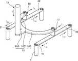
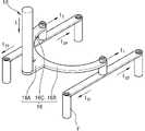
도 6은 4개의 피드 RF 로드들과 함께 그라운드 쉴드가 설치된 플라즈마 공급부를 도시한 사시도이다.
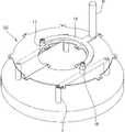
도 7은 도 6에 설치된 그라운드 쉴드만을 따로 도시한 사시도이다.
도 8은 본 발명의 기술적 사상에 의한 실시예들에 따른 기판 처리 장치를 개략적으로 나타낸다.
도 9는 도 8의 기판 처리 장치의 플라즈마 공급부 부분을 보다 구체적으로 도시한다.
Claims (19)
- 삭제
- 삭제
- 삭제
- 삭제
- 삭제
- 삭제
- 기판 처리 장치로서,
기체 유입구;
기판 지지부를 포함하는 반응기로서, 상기 기체 유입구는 상기 기판 지지부에 대해 수직이며 상기 기판 지지부의 중심에 배치되는, 반응기;
상기 기체 유입구에 연결된 기체 공급 수단; 및
상기 기체 공급 수단과 전기적으로 연결된 플라즈마 공급부를 포함하고,
상기 플라즈마 공급부는,
플라즈마 생성부;
상기 플라즈마 생성부와 연결된 RF 로드(RF rod);
상기 RF 로드와 연결되며, 상기 기체 유입구를 둘러싸도록 연장되고 아치 형상을 갖는 브릿지(bridge)로서, 상기 브릿지는 상기 기체 유입구에 대하여 반시계 방향으로 연장되는 반시계 방향 연장부 및 상기 기체 유입구에 대하여 시계 방향으로 연장되는 시계 방향 연장부를 포함하는, 브릿지;
상기 기체 유입구를 중심으로 대칭적으로 배치되는 복수의 피드들; 및
상기 브릿지와 상기 복수의 피드들 사이에 배치된 그라운드 쉴드를 포함하고,
상기 복수의 피드들은,
수평 방향으로 그리고 길이 방향으로 연장되는 제1 피드로서, 상기 제1 피드의 적어도 일부는 상기 브릿지의 제1 단부와 수직 방향에서 중첩되는, 제1 피드;
상기 제1 피드가 연장되는 방향과 반대 방향으로 연장되는 제2 피드;
수평 방향으로 그리고 길이 방향으로 연장되는 제3 피드로서, 상기 제3 피드의 적어도 일부는 상기 브릿지의 제2 단부와 수직 방향에서 중첩되는, 제3 피드; 및
상기 제3 피드가 연장되는 방향과 반대 방향으로 연장되는 제4 피드를 포함하고,
상기 기판 처리 장치의 상기 플라즈마 공급부는,
상기 반시계 방향 연장부와 상기 제1 피드 및 상기 제2 피드를 연결하는 제1 분기점(first split point); 및
상기 시계 방향 연장부와 상기 제3 피드 및 상기 제4 피드를 연결하는 제2 분기점(second split point)을 더 포함하고,
상기 반시계 방향 연장부를 통해 흐르는 제1 전류는 상기 제1 피드를 통해 흐르는 제2 전류의 방향과 반대 방향으로 흐르고,
상기 시계 방향 연장부를 통해 흐르는 제3 전류는 상기 제3 피드를 통해 흐르는 제4 전류의 방향과 반대 방향으로 흐르며,
상기 제1 전류 및 상기 제3 전류에 의해 제1 유도 신호 성분이 생성되고, 상기 제2 전류 및 상기 제4 전류에 의해 제2 유도 신호 성분이 생성되며,
상기 그라운드 쉴드는 상기 제1 유도 신호 성분 및 상기 제2 유도 신호 성분을 방전하도록 구성되고,
상기 기체 유입구는 상기 반응기의 상부에 연결된 상기 복수의 피드들 사이에 배치되며,
상기 브릿지는 상기 반시계 방향 연장부 및 상기 시계 방향 연장부를 통해 상기 기체 유입구를 둘러싸며,
상기 제1 피드, 상기 제2 피드, 상기 제3 피드, 및 상기 제4 피드는 상기 브릿지를 통해 상기 RF 로드에 연결되는 것을 특징으로 하는, 기판 처리 장치. - 삭제
- 삭제
- 청구항 7에 있어서,
상기 피드들과 상기 기체 공급수단을 전기적으로 연결하는 복수개의 피드 RF 로드;를 더 포함하며 상기 피드들 및 피드 RF 로드들은 상기 기체 유입구를 중심으로 대칭적으로 배치된 것;을 특징으로 하는 기판 처리 장치. - 플라즈마 공급부를 포함하는 기판 처리 장치로서,
상기 플라즈마 공급부는,
RF 로드(main RF rod);
상기 RF 로드와 연결되고 아치 형상을 갖는 브릿지(bridge)로서, 상기 브릿지는 반시계 방향 연장부 및 시계 방향 연장부를 포함하는, 브릿지;
복수개의 피드들(RF feeds); 및
상기 브릿지 및 상기 복수개의 피드들 사이에 배치된 그라운드 쉴드;를 포함하며, 상기 플라즈마 공급부는 반응기의 상부와 연결되고,
상기 복수의 피드들은,
수평 방향으로 그리고 길이 방향으로 연장되는 제1 피드로서, 상기 제1 피드의 적어도 일부는 상기 브릿지의 제1 단부와 수직 방향에서 중첩되는, 제1 피드;
상기 제1 피드가 연장되는 방향과 반대 방향으로 연장되는 제2 피드;
수평 방향으로 그리고 길이 방향으로 연장되는 제3 피드로서, 상기 제3 피드의 적어도 일부는 상기 브릿지의 제2 단부와 수직 방향에서 중첩되는, 제3 피드; 및
상기 제3 피드가 연장되는 방향과 반대 방향으로 연장되는 제4 피드를 포함하고,
상기 기판 처리 장치는,
상기 반시계 방향 연장부와 상기 제1 피드 및 상기 제2 피드를 연결하는 제1 분기점(first split point); 및
상기 시계 방향 연장부와 상기 제3 피드 및 상기 제4 피드를 연결하는 제2 분기점(second split point)을 포함하고,
상기 반시계 방향 연장부를 통해 흐르는 제1 전류는 상기 제1 피드를 통해 흐르는 제2 전류의 방향과 반대 방향으로 흐르고,
상기 시계 방향 연장부를 통해 흐르는 제3 전류는 상기 제3 피드를 통해 흐르는 제4 전류의 방향과 반대 방향으로 흐르며,
상기 제1 전류 및 상기 제3 전류에 의해 제1 유도 신호 성분이 생성되고, 상기 제2 전류 및 상기 제4 전류에 의해 제2 유도 신호 성분이 생성되며,
상기 그라운드 쉴드는 상기 제1 유도 신호 성분 및 상기 제2 유도 신호 성분을 방전하도록 구성되고,
상기 기판 처리 장치는 상기 반응기의 상부에 연결된 상기 복수의 피드들 사이에 배치된 기체 유입구를 더 포함하며,
상기 기체 유입구는 상기 반응기 내에 위치된 기판 지지부에 대해 수직이며 상기 기판 지지부의 중심에 배치되고,
상기 브릿지는 상기 반시계 방향 연장부 및 상기 시계 방향 연장부를 통해 상기 기체 유입구를 둘러싸며,
상기 제1 피드, 상기 제2 피드, 상기 제3 피드, 및 상기 제4 피드는 상기 브릿지를 통해 상기 RF 로드에 연결된 것을 특징으로 하는 기판 처리 장치. - 청구항 11에 있어서,
상기 RF 로드와 상기 브릿지는 서로 연결되며;
상기 브릿지와 상기 복수개의 피드들은 상기 제1 분기점(first split point) 및 상기 제2 분기점(second split point)에서 서로 연결되며,
RF 전류는 상기 RF 로드, 상기 브릿지, 상기 제1 분기점, 상기 제2 분기점, 및 상기 복수개의 피드들을 통해 상기 반응기로 공급되는 것을 특징으로 하는 기판 처리 장치. - 청구항 12에 있어서,
상기 복수개의 피드들은 상기 기판 처리 장치의 중심을 기준으로 대칭적으로 배치된 것을 특징으로 하는 기판 처리 장치. - 청구항 11에 있어서,
상기 그라운드 쉴드는 금속으로 이루어진 것을 특징으로 하는 기판 처리 장치. - 청구항 14에 있어서,
상기 그라운드 쉴드는 알루미늄으로 이루어진 것을 특징으로 하는 기판 처리 장치. - 청구항 11에 있어서,
상기 그라운드 쉴드는 상기 브릿지와 상기 피드들 사이에 형성되는 크로스토크(cross-talk)를 방지하는 것을 특징으로 하는 기판 처리 장치. - 청구항 11에 있어서,
60MHz의 이상의 주파수를 갖는 플라즈마를 생성하는 플라즈마 생성부를 더 포함하는 것을 특징으로 하는 기판 처리 장치. - 청구항 11에 있어서,
상기 그라운드 쉴드는 제1 패널 및 제2 패널을 포함하고,
상기 제1 패널과 상기 제2 패널을 상기 기체 유입구의 양 측면에 배치하고 상기 제1 패널 및 상기 제2 패널을 조립함으로써 상기 기체 유입구를 둘러싸는 그라운드 쉴드 구조가 형성되는 것을 특징으로 하는 기판 처리 장치. - 청구항 11에 있어서,
상기 복수개의 피드들과 상기 반응기 상부를 전기적으로 연결하는 복수개의 피드 RF 로드들;을 더 포함하며 상기 피드들과 상기 피드 RF로드들은 상기 반응기상부의 중심을 기준으로 대칭적으로 배치된 것;을 특징으로 하는 기판 처리 장치.
Priority Applications (4)
| Application Number | Priority Date | Filing Date | Title |
|---|---|---|---|
| KR1020170110341AKR102491945B1 (ko) | 2017-08-30 | 2017-08-30 | 기판 처리 장치 |
| TW107127688ATWI719333B (zh) | 2017-08-30 | 2018-08-08 | 基板處理設備 |
| CN201810994464.7ACN109427533B (zh) | 2017-08-30 | 2018-08-29 | 衬底处理设备 |
| US16/116,708US11069510B2 (en) | 2017-08-30 | 2018-08-29 | Substrate processing apparatus |
Applications Claiming Priority (1)
| Application Number | Priority Date | Filing Date | Title |
|---|---|---|---|
| KR1020170110341AKR102491945B1 (ko) | 2017-08-30 | 2017-08-30 | 기판 처리 장치 |
Publications (2)
| Publication Number | Publication Date |
|---|---|
| KR20190023920A KR20190023920A (ko) | 2019-03-08 |
| KR102491945B1true KR102491945B1 (ko) | 2023-01-26 |
Family
ID=65434350
Family Applications (1)
| Application Number | Title | Priority Date | Filing Date |
|---|---|---|---|
| KR1020170110341AActiveKR102491945B1 (ko) | 2017-08-30 | 2017-08-30 | 기판 처리 장치 |
Country Status (4)
| Country | Link |
|---|---|
| US (1) | US11069510B2 (ko) |
| KR (1) | KR102491945B1 (ko) |
| CN (1) | CN109427533B (ko) |
| TW (1) | TWI719333B (ko) |
Families Citing this family (320)
| Publication number | Priority date | Publication date | Assignee | Title |
|---|---|---|---|---|
| US9394608B2 (en) | 2009-04-06 | 2016-07-19 | Asm America, Inc. | Semiconductor processing reactor and components thereof |
| US8802201B2 (en) | 2009-08-14 | 2014-08-12 | Asm America, Inc. | Systems and methods for thin-film deposition of metal oxides using excited nitrogen-oxygen species |
| US9312155B2 (en) | 2011-06-06 | 2016-04-12 | Asm Japan K.K. | High-throughput semiconductor-processing apparatus equipped with multiple dual-chamber modules |
| US10854498B2 (en) | 2011-07-15 | 2020-12-01 | Asm Ip Holding B.V. | Wafer-supporting device and method for producing same |
| US20130023129A1 (en) | 2011-07-20 | 2013-01-24 | Asm America, Inc. | Pressure transmitter for a semiconductor processing environment |
| US9017481B1 (en) | 2011-10-28 | 2015-04-28 | Asm America, Inc. | Process feed management for semiconductor substrate processing |
| US10714315B2 (en) | 2012-10-12 | 2020-07-14 | Asm Ip Holdings B.V. | Semiconductor reaction chamber showerhead |
| US20160376700A1 (en) | 2013-02-01 | 2016-12-29 | Asm Ip Holding B.V. | System for treatment of deposition reactor |
| US10683571B2 (en) | 2014-02-25 | 2020-06-16 | Asm Ip Holding B.V. | Gas supply manifold and method of supplying gases to chamber using same |
| US10167557B2 (en) | 2014-03-18 | 2019-01-01 | Asm Ip Holding B.V. | Gas distribution system, reactor including the system, and methods of using the same |
| US11015245B2 (en) | 2014-03-19 | 2021-05-25 | Asm Ip Holding B.V. | Gas-phase reactor and system having exhaust plenum and components thereof |
| US10858737B2 (en)* | 2014-07-28 | 2020-12-08 | Asm Ip Holding B.V. | Showerhead assembly and components thereof |
| US9890456B2 (en) | 2014-08-21 | 2018-02-13 | Asm Ip Holding B.V. | Method and system for in situ formation of gas-phase compounds |
| US10941490B2 (en) | 2014-10-07 | 2021-03-09 | Asm Ip Holding B.V. | Multiple temperature range susceptor, assembly, reactor and system including the susceptor, and methods of using the same |
| US9657845B2 (en) | 2014-10-07 | 2017-05-23 | Asm Ip Holding B.V. | Variable conductance gas distribution apparatus and method |
| US10276355B2 (en) | 2015-03-12 | 2019-04-30 | Asm Ip Holding B.V. | Multi-zone reactor, system including the reactor, and method of using the same |
| US10458018B2 (en) | 2015-06-26 | 2019-10-29 | Asm Ip Holding B.V. | Structures including metal carbide material, devices including the structures, and methods of forming same |
| US10600673B2 (en) | 2015-07-07 | 2020-03-24 | Asm Ip Holding B.V. | Magnetic susceptor to baseplate seal |
| US10211308B2 (en) | 2015-10-21 | 2019-02-19 | Asm Ip Holding B.V. | NbMC layers |
| US11139308B2 (en) | 2015-12-29 | 2021-10-05 | Asm Ip Holding B.V. | Atomic layer deposition of III-V compounds to form V-NAND devices |
| US10529554B2 (en) | 2016-02-19 | 2020-01-07 | Asm Ip Holding B.V. | Method for forming silicon nitride film selectively on sidewalls or flat surfaces of trenches |
| US10343920B2 (en) | 2016-03-18 | 2019-07-09 | Asm Ip Holding B.V. | Aligned carbon nanotubes |
| US10190213B2 (en) | 2016-04-21 | 2019-01-29 | Asm Ip Holding B.V. | Deposition of metal borides |
| US10865475B2 (en) | 2016-04-21 | 2020-12-15 | Asm Ip Holding B.V. | Deposition of metal borides and silicides |
| US10032628B2 (en) | 2016-05-02 | 2018-07-24 | Asm Ip Holding B.V. | Source/drain performance through conformal solid state doping |
| US10367080B2 (en) | 2016-05-02 | 2019-07-30 | Asm Ip Holding B.V. | Method of forming a germanium oxynitride film |
| US11453943B2 (en) | 2016-05-25 | 2022-09-27 | Asm Ip Holding B.V. | Method for forming carbon-containing silicon/metal oxide or nitride film by ALD using silicon precursor and hydrocarbon precursor |
| US10612137B2 (en) | 2016-07-08 | 2020-04-07 | Asm Ip Holdings B.V. | Organic reactants for atomic layer deposition |
| US9859151B1 (en) | 2016-07-08 | 2018-01-02 | Asm Ip Holding B.V. | Selective film deposition method to form air gaps |
| US10714385B2 (en) | 2016-07-19 | 2020-07-14 | Asm Ip Holding B.V. | Selective deposition of tungsten |
| KR102532607B1 (ko) | 2016-07-28 | 2023-05-15 | 에이에스엠 아이피 홀딩 비.브이. | 기판 가공 장치 및 그 동작 방법 |
| US9812320B1 (en) | 2016-07-28 | 2017-11-07 | Asm Ip Holding B.V. | Method and apparatus for filling a gap |
| US9887082B1 (en) | 2016-07-28 | 2018-02-06 | Asm Ip Holding B.V. | Method and apparatus for filling a gap |
| US10643826B2 (en) | 2016-10-26 | 2020-05-05 | Asm Ip Holdings B.V. | Methods for thermally calibrating reaction chambers |
| US11532757B2 (en) | 2016-10-27 | 2022-12-20 | Asm Ip Holding B.V. | Deposition of charge trapping layers |
| US10229833B2 (en) | 2016-11-01 | 2019-03-12 | Asm Ip Holding B.V. | Methods for forming a transition metal nitride film on a substrate by atomic layer deposition and related semiconductor device structures |
| US10714350B2 (en) | 2016-11-01 | 2020-07-14 | ASM IP Holdings, B.V. | Methods for forming a transition metal niobium nitride film on a substrate by atomic layer deposition and related semiconductor device structures |
| US10643904B2 (en) | 2016-11-01 | 2020-05-05 | Asm Ip Holdings B.V. | Methods for forming a semiconductor device and related semiconductor device structures |
| US10134757B2 (en) | 2016-11-07 | 2018-11-20 | Asm Ip Holding B.V. | Method of processing a substrate and a device manufactured by using the method |
| KR102546317B1 (ko) | 2016-11-15 | 2023-06-21 | 에이에스엠 아이피 홀딩 비.브이. | 기체 공급 유닛 및 이를 포함하는 기판 처리 장치 |
| KR102762543B1 (ko)* | 2016-12-14 | 2025-02-05 | 에이에스엠 아이피 홀딩 비.브이. | 기판 처리 장치 |
| US11447861B2 (en) | 2016-12-15 | 2022-09-20 | Asm Ip Holding B.V. | Sequential infiltration synthesis apparatus and a method of forming a patterned structure |
| US11581186B2 (en) | 2016-12-15 | 2023-02-14 | Asm Ip Holding B.V. | Sequential infiltration synthesis apparatus |
| KR102700194B1 (ko) | 2016-12-19 | 2024-08-28 | 에이에스엠 아이피 홀딩 비.브이. | 기판 처리 장치 |
| US10269558B2 (en) | 2016-12-22 | 2019-04-23 | Asm Ip Holding B.V. | Method of forming a structure on a substrate |
| US10867788B2 (en) | 2016-12-28 | 2020-12-15 | Asm Ip Holding B.V. | Method of forming a structure on a substrate |
| US11390950B2 (en) | 2017-01-10 | 2022-07-19 | Asm Ip Holding B.V. | Reactor system and method to reduce residue buildup during a film deposition process |
| US10655221B2 (en) | 2017-02-09 | 2020-05-19 | Asm Ip Holding B.V. | Method for depositing oxide film by thermal ALD and PEALD |
| US10468261B2 (en) | 2017-02-15 | 2019-11-05 | Asm Ip Holding B.V. | Methods for forming a metallic film on a substrate by cyclical deposition and related semiconductor device structures |
| US10529563B2 (en) | 2017-03-29 | 2020-01-07 | Asm Ip Holdings B.V. | Method for forming doped metal oxide films on a substrate by cyclical deposition and related semiconductor device structures |
| USD876504S1 (en) | 2017-04-03 | 2020-02-25 | Asm Ip Holding B.V. | Exhaust flow control ring for semiconductor deposition apparatus |
| KR102457289B1 (ko) | 2017-04-25 | 2022-10-21 | 에이에스엠 아이피 홀딩 비.브이. | 박막 증착 방법 및 반도체 장치의 제조 방법 |
| US10770286B2 (en) | 2017-05-08 | 2020-09-08 | Asm Ip Holdings B.V. | Methods for selectively forming a silicon nitride film on a substrate and related semiconductor device structures |
| US10892156B2 (en) | 2017-05-08 | 2021-01-12 | Asm Ip Holding B.V. | Methods for forming a silicon nitride film on a substrate and related semiconductor device structures |
| US10886123B2 (en) | 2017-06-02 | 2021-01-05 | Asm Ip Holding B.V. | Methods for forming low temperature semiconductor layers and related semiconductor device structures |
| US12040200B2 (en) | 2017-06-20 | 2024-07-16 | Asm Ip Holding B.V. | Semiconductor processing apparatus and methods for calibrating a semiconductor processing apparatus |
| US11306395B2 (en) | 2017-06-28 | 2022-04-19 | Asm Ip Holding B.V. | Methods for depositing a transition metal nitride film on a substrate by atomic layer deposition and related deposition apparatus |
| US10685834B2 (en) | 2017-07-05 | 2020-06-16 | Asm Ip Holdings B.V. | Methods for forming a silicon germanium tin layer and related semiconductor device structures |
| KR20190009245A (ko) | 2017-07-18 | 2019-01-28 | 에이에스엠 아이피 홀딩 비.브이. | 반도체 소자 구조물 형성 방법 및 관련된 반도체 소자 구조물 |
| US11018002B2 (en) | 2017-07-19 | 2021-05-25 | Asm Ip Holding B.V. | Method for selectively depositing a Group IV semiconductor and related semiconductor device structures |
| US10541333B2 (en) | 2017-07-19 | 2020-01-21 | Asm Ip Holding B.V. | Method for depositing a group IV semiconductor and related semiconductor device structures |
| US11374112B2 (en) | 2017-07-19 | 2022-06-28 | Asm Ip Holding B.V. | Method for depositing a group IV semiconductor and related semiconductor device structures |
| US10590535B2 (en) | 2017-07-26 | 2020-03-17 | Asm Ip Holdings B.V. | Chemical treatment, deposition and/or infiltration apparatus and method for using the same |
| TWI815813B (zh) | 2017-08-04 | 2023-09-21 | 荷蘭商Asm智慧財產控股公司 | 用於分配反應腔內氣體的噴頭總成 |
| US10692741B2 (en) | 2017-08-08 | 2020-06-23 | Asm Ip Holdings B.V. | Radiation shield |
| US10770336B2 (en) | 2017-08-08 | 2020-09-08 | Asm Ip Holding B.V. | Substrate lift mechanism and reactor including same |
| US10249524B2 (en) | 2017-08-09 | 2019-04-02 | Asm Ip Holding B.V. | Cassette holder assembly for a substrate cassette and holding member for use in such assembly |
| US11139191B2 (en) | 2017-08-09 | 2021-10-05 | Asm Ip Holding B.V. | Storage apparatus for storing cassettes for substrates and processing apparatus equipped therewith |
| US11769682B2 (en) | 2017-08-09 | 2023-09-26 | Asm Ip Holding B.V. | Storage apparatus for storing cassettes for substrates and processing apparatus equipped therewith |
| USD900036S1 (en) | 2017-08-24 | 2020-10-27 | Asm Ip Holding B.V. | Heater electrical connector and adapter |
| US11830730B2 (en) | 2017-08-29 | 2023-11-28 | Asm Ip Holding B.V. | Layer forming method and apparatus |
| KR102491945B1 (ko) | 2017-08-30 | 2023-01-26 | 에이에스엠 아이피 홀딩 비.브이. | 기판 처리 장치 |
| US11056344B2 (en) | 2017-08-30 | 2021-07-06 | Asm Ip Holding B.V. | Layer forming method |
| US11295980B2 (en) | 2017-08-30 | 2022-04-05 | Asm Ip Holding B.V. | Methods for depositing a molybdenum metal film over a dielectric surface of a substrate by a cyclical deposition process and related semiconductor device structures |
| KR102401446B1 (ko) | 2017-08-31 | 2022-05-24 | 에이에스엠 아이피 홀딩 비.브이. | 기판 처리 장치 |
| KR102630301B1 (ko) | 2017-09-21 | 2024-01-29 | 에이에스엠 아이피 홀딩 비.브이. | 침투성 재료의 순차 침투 합성 방법 처리 및 이를 이용하여 형성된 구조물 및 장치 |
| US10844484B2 (en) | 2017-09-22 | 2020-11-24 | Asm Ip Holding B.V. | Apparatus for dispensing a vapor phase reactant to a reaction chamber and related methods |
| US10658205B2 (en) | 2017-09-28 | 2020-05-19 | Asm Ip Holdings B.V. | Chemical dispensing apparatus and methods for dispensing a chemical to a reaction chamber |
| US10403504B2 (en) | 2017-10-05 | 2019-09-03 | Asm Ip Holding B.V. | Method for selectively depositing a metallic film on a substrate |
| US10319588B2 (en) | 2017-10-10 | 2019-06-11 | Asm Ip Holding B.V. | Method for depositing a metal chalcogenide on a substrate by cyclical deposition |
| US10923344B2 (en) | 2017-10-30 | 2021-02-16 | Asm Ip Holding B.V. | Methods for forming a semiconductor structure and related semiconductor structures |
| KR102443047B1 (ko) | 2017-11-16 | 2022-09-14 | 에이에스엠 아이피 홀딩 비.브이. | 기판 처리 장치 방법 및 그에 의해 제조된 장치 |
| US10910262B2 (en) | 2017-11-16 | 2021-02-02 | Asm Ip Holding B.V. | Method of selectively depositing a capping layer structure on a semiconductor device structure |
| US11022879B2 (en) | 2017-11-24 | 2021-06-01 | Asm Ip Holding B.V. | Method of forming an enhanced unexposed photoresist layer |
| CN111344522B (zh) | 2017-11-27 | 2022-04-12 | 阿斯莫Ip控股公司 | 包括洁净迷你环境的装置 |
| WO2019103613A1 (en) | 2017-11-27 | 2019-05-31 | Asm Ip Holding B.V. | A storage device for storing wafer cassettes for use with a batch furnace |
| US10872771B2 (en) | 2018-01-16 | 2020-12-22 | Asm Ip Holding B. V. | Method for depositing a material film on a substrate within a reaction chamber by a cyclical deposition process and related device structures |
| KR102695659B1 (ko) | 2018-01-19 | 2024-08-14 | 에이에스엠 아이피 홀딩 비.브이. | 플라즈마 보조 증착에 의해 갭 충진 층을 증착하는 방법 |
| TWI799494B (zh) | 2018-01-19 | 2023-04-21 | 荷蘭商Asm 智慧財產控股公司 | 沈積方法 |
| USD903477S1 (en) | 2018-01-24 | 2020-12-01 | Asm Ip Holdings B.V. | Metal clamp |
| US11018047B2 (en) | 2018-01-25 | 2021-05-25 | Asm Ip Holding B.V. | Hybrid lift pin |
| USD880437S1 (en) | 2018-02-01 | 2020-04-07 | Asm Ip Holding B.V. | Gas supply plate for semiconductor manufacturing apparatus |
| US11081345B2 (en) | 2018-02-06 | 2021-08-03 | Asm Ip Holding B.V. | Method of post-deposition treatment for silicon oxide film |
| WO2019158960A1 (en) | 2018-02-14 | 2019-08-22 | Asm Ip Holding B.V. | A method for depositing a ruthenium-containing film on a substrate by a cyclical deposition process |
| US10896820B2 (en) | 2018-02-14 | 2021-01-19 | Asm Ip Holding B.V. | Method for depositing a ruthenium-containing film on a substrate by a cyclical deposition process |
| US10731249B2 (en) | 2018-02-15 | 2020-08-04 | Asm Ip Holding B.V. | Method of forming a transition metal containing film on a substrate by a cyclical deposition process, a method for supplying a transition metal halide compound to a reaction chamber, and related vapor deposition apparatus |
| US10658181B2 (en) | 2018-02-20 | 2020-05-19 | Asm Ip Holding B.V. | Method of spacer-defined direct patterning in semiconductor fabrication |
| KR102636427B1 (ko)* | 2018-02-20 | 2024-02-13 | 에이에스엠 아이피 홀딩 비.브이. | 기판 처리 방법 및 장치 |
| US10975470B2 (en) | 2018-02-23 | 2021-04-13 | Asm Ip Holding B.V. | Apparatus for detecting or monitoring for a chemical precursor in a high temperature environment |
| US11473195B2 (en) | 2018-03-01 | 2022-10-18 | Asm Ip Holding B.V. | Semiconductor processing apparatus and a method for processing a substrate |
| US11629406B2 (en) | 2018-03-09 | 2023-04-18 | Asm Ip Holding B.V. | Semiconductor processing apparatus comprising one or more pyrometers for measuring a temperature of a substrate during transfer of the substrate |
| US11114283B2 (en) | 2018-03-16 | 2021-09-07 | Asm Ip Holding B.V. | Reactor, system including the reactor, and methods of manufacturing and using same |
| KR102646467B1 (ko) | 2018-03-27 | 2024-03-11 | 에이에스엠 아이피 홀딩 비.브이. | 기판 상에 전극을 형성하는 방법 및 전극을 포함하는 반도체 소자 구조 |
| US11088002B2 (en) | 2018-03-29 | 2021-08-10 | Asm Ip Holding B.V. | Substrate rack and a substrate processing system and method |
| US11230766B2 (en) | 2018-03-29 | 2022-01-25 | Asm Ip Holding B.V. | Substrate processing apparatus and method |
| KR102501472B1 (ko) | 2018-03-30 | 2023-02-20 | 에이에스엠 아이피 홀딩 비.브이. | 기판 처리 방법 |
| KR102600229B1 (ko) | 2018-04-09 | 2023-11-10 | 에이에스엠 아이피 홀딩 비.브이. | 기판 지지 장치, 이를 포함하는 기판 처리 장치 및 기판 처리 방법 |
| TWI811348B (zh) | 2018-05-08 | 2023-08-11 | 荷蘭商Asm 智慧財產控股公司 | 藉由循環沉積製程於基板上沉積氧化物膜之方法及相關裝置結構 |
| US12025484B2 (en) | 2018-05-08 | 2024-07-02 | Asm Ip Holding B.V. | Thin film forming method |
| US12272527B2 (en) | 2018-05-09 | 2025-04-08 | Asm Ip Holding B.V. | Apparatus for use with hydrogen radicals and method of using same |
| KR20190129718A (ko) | 2018-05-11 | 2019-11-20 | 에이에스엠 아이피 홀딩 비.브이. | 기판 상에 피도핑 금속 탄화물 막을 형성하는 방법 및 관련 반도체 소자 구조 |
| KR102596988B1 (ko) | 2018-05-28 | 2023-10-31 | 에이에스엠 아이피 홀딩 비.브이. | 기판 처리 방법 및 그에 의해 제조된 장치 |
| US11718913B2 (en) | 2018-06-04 | 2023-08-08 | Asm Ip Holding B.V. | Gas distribution system and reactor system including same |
| TWI840362B (zh) | 2018-06-04 | 2024-05-01 | 荷蘭商Asm Ip私人控股有限公司 | 水氣降低的晶圓處置腔室 |
| US11286562B2 (en) | 2018-06-08 | 2022-03-29 | Asm Ip Holding B.V. | Gas-phase chemical reactor and method of using same |
| KR102568797B1 (ko) | 2018-06-21 | 2023-08-21 | 에이에스엠 아이피 홀딩 비.브이. | 기판 처리 시스템 |
| US10797133B2 (en) | 2018-06-21 | 2020-10-06 | Asm Ip Holding B.V. | Method for depositing a phosphorus doped silicon arsenide film and related semiconductor device structures |
| TWI873894B (zh) | 2018-06-27 | 2025-02-21 | 荷蘭商Asm Ip私人控股有限公司 | 用於形成含金屬材料及包含含金屬材料的膜及結構之循環沉積方法 |
| KR102854019B1 (ko) | 2018-06-27 | 2025-09-02 | 에이에스엠 아이피 홀딩 비.브이. | 금속 함유 재료를 형성하기 위한 주기적 증착 방법 및 금속 함유 재료를 포함하는 필름 및 구조체 |
| US10612136B2 (en) | 2018-06-29 | 2020-04-07 | ASM IP Holding, B.V. | Temperature-controlled flange and reactor system including same |
| KR102686758B1 (ko) | 2018-06-29 | 2024-07-18 | 에이에스엠 아이피 홀딩 비.브이. | 박막 증착 방법 및 반도체 장치의 제조 방법 |
| US10388513B1 (en) | 2018-07-03 | 2019-08-20 | Asm Ip Holding B.V. | Method for depositing silicon-free carbon-containing film as gap-fill layer by pulse plasma-assisted deposition |
| US10755922B2 (en) | 2018-07-03 | 2020-08-25 | Asm Ip Holding B.V. | Method for depositing silicon-free carbon-containing film as gap-fill layer by pulse plasma-assisted deposition |
| US10767789B2 (en) | 2018-07-16 | 2020-09-08 | Asm Ip Holding B.V. | Diaphragm valves, valve components, and methods for forming valve components |
| US11053591B2 (en) | 2018-08-06 | 2021-07-06 | Asm Ip Holding B.V. | Multi-port gas injection system and reactor system including same |
| US10883175B2 (en) | 2018-08-09 | 2021-01-05 | Asm Ip Holding B.V. | Vertical furnace for processing substrates and a liner for use therein |
| US10829852B2 (en) | 2018-08-16 | 2020-11-10 | Asm Ip Holding B.V. | Gas distribution device for a wafer processing apparatus |
| US11430674B2 (en) | 2018-08-22 | 2022-08-30 | Asm Ip Holding B.V. | Sensor array, apparatus for dispensing a vapor phase reactant to a reaction chamber and related methods |
| KR102707956B1 (ko) | 2018-09-11 | 2024-09-19 | 에이에스엠 아이피 홀딩 비.브이. | 박막 증착 방법 |
| US11024523B2 (en) | 2018-09-11 | 2021-06-01 | Asm Ip Holding B.V. | Substrate processing apparatus and method |
| US11049751B2 (en) | 2018-09-14 | 2021-06-29 | Asm Ip Holding B.V. | Cassette supply system to store and handle cassettes and processing apparatus equipped therewith |
| CN110970344B (zh) | 2018-10-01 | 2024-10-25 | Asmip控股有限公司 | 衬底保持设备、包含所述设备的系统及其使用方法 |
| US11232963B2 (en) | 2018-10-03 | 2022-01-25 | Asm Ip Holding B.V. | Substrate processing apparatus and method |
| KR102592699B1 (ko) | 2018-10-08 | 2023-10-23 | 에이에스엠 아이피 홀딩 비.브이. | 기판 지지 유닛 및 이를 포함하는 박막 증착 장치와 기판 처리 장치 |
| US10847365B2 (en) | 2018-10-11 | 2020-11-24 | Asm Ip Holding B.V. | Method of forming conformal silicon carbide film by cyclic CVD |
| US10811256B2 (en) | 2018-10-16 | 2020-10-20 | Asm Ip Holding B.V. | Method for etching a carbon-containing feature |
| KR102605121B1 (ko) | 2018-10-19 | 2023-11-23 | 에이에스엠 아이피 홀딩 비.브이. | 기판 처리 장치 및 기판 처리 방법 |
| KR102546322B1 (ko) | 2018-10-19 | 2023-06-21 | 에이에스엠 아이피 홀딩 비.브이. | 기판 처리 장치 및 기판 처리 방법 |
| USD948463S1 (en) | 2018-10-24 | 2022-04-12 | Asm Ip Holding B.V. | Susceptor for semiconductor substrate supporting apparatus |
| US12378665B2 (en) | 2018-10-26 | 2025-08-05 | Asm Ip Holding B.V. | High temperature coatings for a preclean and etch apparatus and related methods |
| US11087997B2 (en) | 2018-10-31 | 2021-08-10 | Asm Ip Holding B.V. | Substrate processing apparatus for processing substrates |
| KR102748291B1 (ko) | 2018-11-02 | 2024-12-31 | 에이에스엠 아이피 홀딩 비.브이. | 기판 지지 유닛 및 이를 포함하는 기판 처리 장치 |
| US11572620B2 (en) | 2018-11-06 | 2023-02-07 | Asm Ip Holding B.V. | Methods for selectively depositing an amorphous silicon film on a substrate |
| US11031242B2 (en) | 2018-11-07 | 2021-06-08 | Asm Ip Holding B.V. | Methods for depositing a boron doped silicon germanium film |
| US10818758B2 (en) | 2018-11-16 | 2020-10-27 | Asm Ip Holding B.V. | Methods for forming a metal silicate film on a substrate in a reaction chamber and related semiconductor device structures |
| US10847366B2 (en) | 2018-11-16 | 2020-11-24 | Asm Ip Holding B.V. | Methods for depositing a transition metal chalcogenide film on a substrate by a cyclical deposition process |
| US10559458B1 (en) | 2018-11-26 | 2020-02-11 | Asm Ip Holding B.V. | Method of forming oxynitride film |
| US12040199B2 (en) | 2018-11-28 | 2024-07-16 | Asm Ip Holding B.V. | Substrate processing apparatus for processing substrates |
| US11217444B2 (en) | 2018-11-30 | 2022-01-04 | Asm Ip Holding B.V. | Method for forming an ultraviolet radiation responsive metal oxide-containing film |
| KR102636428B1 (ko) | 2018-12-04 | 2024-02-13 | 에이에스엠 아이피 홀딩 비.브이. | 기판 처리 장치를 세정하는 방법 |
| US11158513B2 (en) | 2018-12-13 | 2021-10-26 | Asm Ip Holding B.V. | Methods for forming a rhenium-containing film on a substrate by a cyclical deposition process and related semiconductor device structures |
| TWI874340B (zh) | 2018-12-14 | 2025-03-01 | 荷蘭商Asm Ip私人控股有限公司 | 形成裝置結構之方法、其所形成之結構及施行其之系統 |
| TWI866480B (zh) | 2019-01-17 | 2024-12-11 | 荷蘭商Asm Ip 私人控股有限公司 | 藉由循環沈積製程於基板上形成含過渡金屬膜之方法 |
| KR102727227B1 (ko) | 2019-01-22 | 2024-11-07 | 에이에스엠 아이피 홀딩 비.브이. | 기판 처리 장치 |
| CN111524788B (zh) | 2019-02-01 | 2023-11-24 | Asm Ip私人控股有限公司 | 氧化硅的拓扑选择性膜形成的方法 |
| TWI873122B (zh) | 2019-02-20 | 2025-02-21 | 荷蘭商Asm Ip私人控股有限公司 | 填充一基板之一表面內所形成的一凹槽的方法、根據其所形成之半導體結構、及半導體處理設備 |
| KR102626263B1 (ko) | 2019-02-20 | 2024-01-16 | 에이에스엠 아이피 홀딩 비.브이. | 처리 단계를 포함하는 주기적 증착 방법 및 이를 위한 장치 |
| TWI838458B (zh) | 2019-02-20 | 2024-04-11 | 荷蘭商Asm Ip私人控股有限公司 | 用於3d nand應用中之插塞填充沉積之設備及方法 |
| TWI845607B (zh) | 2019-02-20 | 2024-06-21 | 荷蘭商Asm Ip私人控股有限公司 | 用來填充形成於基材表面內之凹部的循環沉積方法及設備 |
| TWI842826B (zh) | 2019-02-22 | 2024-05-21 | 荷蘭商Asm Ip私人控股有限公司 | 基材處理設備及處理基材之方法 |
| KR102782593B1 (ko) | 2019-03-08 | 2025-03-14 | 에이에스엠 아이피 홀딩 비.브이. | SiOC 층을 포함한 구조체 및 이의 형성 방법 |
| US11742198B2 (en) | 2019-03-08 | 2023-08-29 | Asm Ip Holding B.V. | Structure including SiOCN layer and method of forming same |
| KR102858005B1 (ko) | 2019-03-08 | 2025-09-09 | 에이에스엠 아이피 홀딩 비.브이. | 실리콘 질화물 층을 선택적으로 증착하는 방법, 및 선택적으로 증착된 실리콘 질화물 층을 포함하는 구조체 |
| JP2020167398A (ja) | 2019-03-28 | 2020-10-08 | エーエスエム・アイピー・ホールディング・ベー・フェー | ドアオープナーおよびドアオープナーが提供される基材処理装置 |
| KR102809999B1 (ko) | 2019-04-01 | 2025-05-19 | 에이에스엠 아이피 홀딩 비.브이. | 반도체 소자를 제조하는 방법 |
| KR20200123380A (ko) | 2019-04-19 | 2020-10-29 | 에이에스엠 아이피 홀딩 비.브이. | 층 형성 방법 및 장치 |
| KR20200125453A (ko) | 2019-04-24 | 2020-11-04 | 에이에스엠 아이피 홀딩 비.브이. | 기상 반응기 시스템 및 이를 사용하는 방법 |
| KR20200130121A (ko) | 2019-05-07 | 2020-11-18 | 에이에스엠 아이피 홀딩 비.브이. | 딥 튜브가 있는 화학물질 공급원 용기 |
| US11289326B2 (en) | 2019-05-07 | 2022-03-29 | Asm Ip Holding B.V. | Method for reforming amorphous carbon polymer film |
| KR20200130652A (ko) | 2019-05-10 | 2020-11-19 | 에이에스엠 아이피 홀딩 비.브이. | 표면 상에 재료를 증착하는 방법 및 본 방법에 따라 형성된 구조 |
| JP7598201B2 (ja) | 2019-05-16 | 2024-12-11 | エーエスエム・アイピー・ホールディング・ベー・フェー | ウェハボートハンドリング装置、縦型バッチ炉および方法 |
| JP7612342B2 (ja) | 2019-05-16 | 2025-01-14 | エーエスエム・アイピー・ホールディング・ベー・フェー | ウェハボートハンドリング装置、縦型バッチ炉および方法 |
| USD947913S1 (en) | 2019-05-17 | 2022-04-05 | Asm Ip Holding B.V. | Susceptor shaft |
| USD975665S1 (en) | 2019-05-17 | 2023-01-17 | Asm Ip Holding B.V. | Susceptor shaft |
| USD935572S1 (en) | 2019-05-24 | 2021-11-09 | Asm Ip Holding B.V. | Gas channel plate |
| USD922229S1 (en) | 2019-06-05 | 2021-06-15 | Asm Ip Holding B.V. | Device for controlling a temperature of a gas supply unit |
| KR20200141002A (ko) | 2019-06-06 | 2020-12-17 | 에이에스엠 아이피 홀딩 비.브이. | 배기 가스 분석을 포함한 기상 반응기 시스템을 사용하는 방법 |
| KR20200141931A (ko) | 2019-06-10 | 2020-12-21 | 에이에스엠 아이피 홀딩 비.브이. | 석영 에피택셜 챔버를 세정하는 방법 |
| KR20200143254A (ko) | 2019-06-11 | 2020-12-23 | 에이에스엠 아이피 홀딩 비.브이. | 개질 가스를 사용하여 전자 구조를 형성하는 방법, 상기 방법을 수행하기 위한 시스템, 및 상기 방법을 사용하여 형성되는 구조 |
| USD944946S1 (en) | 2019-06-14 | 2022-03-01 | Asm Ip Holding B.V. | Shower plate |
| USD931978S1 (en) | 2019-06-27 | 2021-09-28 | Asm Ip Holding B.V. | Showerhead vacuum transport |
| KR20210005515A (ko) | 2019-07-03 | 2021-01-14 | 에이에스엠 아이피 홀딩 비.브이. | 기판 처리 장치용 온도 제어 조립체 및 이를 사용하는 방법 |
| JP7499079B2 (ja) | 2019-07-09 | 2024-06-13 | エーエスエム・アイピー・ホールディング・ベー・フェー | 同軸導波管を用いたプラズマ装置、基板処理方法 |
| CN112216646A (zh) | 2019-07-10 | 2021-01-12 | Asm Ip私人控股有限公司 | 基板支撑组件及包括其的基板处理装置 |
| KR20210010307A (ko) | 2019-07-16 | 2021-01-27 | 에이에스엠 아이피 홀딩 비.브이. | 기판 처리 장치 |
| KR102860110B1 (ko) | 2019-07-17 | 2025-09-16 | 에이에스엠 아이피 홀딩 비.브이. | 실리콘 게르마늄 구조를 형성하는 방법 |
| KR20210010816A (ko) | 2019-07-17 | 2021-01-28 | 에이에스엠 아이피 홀딩 비.브이. | 라디칼 보조 점화 플라즈마 시스템 및 방법 |
| US11643724B2 (en) | 2019-07-18 | 2023-05-09 | Asm Ip Holding B.V. | Method of forming structures using a neutral beam |
| KR20210010817A (ko) | 2019-07-19 | 2021-01-28 | 에이에스엠 아이피 홀딩 비.브이. | 토폴로지-제어된 비정질 탄소 중합체 막을 형성하는 방법 |
| CN110223904A (zh)* | 2019-07-19 | 2019-09-10 | 江苏鲁汶仪器有限公司 | 一种具有法拉第屏蔽装置的等离子体处理系统 |
| TWI839544B (zh) | 2019-07-19 | 2024-04-21 | 荷蘭商Asm Ip私人控股有限公司 | 形成形貌受控的非晶碳聚合物膜之方法 |
| TWI851767B (zh) | 2019-07-29 | 2024-08-11 | 荷蘭商Asm Ip私人控股有限公司 | 用於利用n型摻雜物及/或替代摻雜物選擇性沉積以達成高摻雜物併入之方法 |
| CN112309900A (zh) | 2019-07-30 | 2021-02-02 | Asm Ip私人控股有限公司 | 基板处理设备 |
| US12169361B2 (en) | 2019-07-30 | 2024-12-17 | Asm Ip Holding B.V. | Substrate processing apparatus and method |
| CN112309899A (zh) | 2019-07-30 | 2021-02-02 | Asm Ip私人控股有限公司 | 基板处理设备 |
| US11587815B2 (en) | 2019-07-31 | 2023-02-21 | Asm Ip Holding B.V. | Vertical batch furnace assembly |
| US11227782B2 (en) | 2019-07-31 | 2022-01-18 | Asm Ip Holding B.V. | Vertical batch furnace assembly |
| US11587814B2 (en) | 2019-07-31 | 2023-02-21 | Asm Ip Holding B.V. | Vertical batch furnace assembly |
| CN112323048B (zh) | 2019-08-05 | 2024-02-09 | Asm Ip私人控股有限公司 | 用于化学源容器的液位传感器 |
| CN112342526A (zh) | 2019-08-09 | 2021-02-09 | Asm Ip私人控股有限公司 | 包括冷却装置的加热器组件及其使用方法 |
| USD965524S1 (en) | 2019-08-19 | 2022-10-04 | Asm Ip Holding B.V. | Susceptor support |
| USD965044S1 (en) | 2019-08-19 | 2022-09-27 | Asm Ip Holding B.V. | Susceptor shaft |
| JP2021031769A (ja) | 2019-08-21 | 2021-03-01 | エーエスエム アイピー ホールディング ビー.ブイ. | 成膜原料混合ガス生成装置及び成膜装置 |
| USD930782S1 (en) | 2019-08-22 | 2021-09-14 | Asm Ip Holding B.V. | Gas distributor |
| USD949319S1 (en) | 2019-08-22 | 2022-04-19 | Asm Ip Holding B.V. | Exhaust duct |
| KR20210024423A (ko) | 2019-08-22 | 2021-03-05 | 에이에스엠 아이피 홀딩 비.브이. | 홀을 구비한 구조체를 형성하기 위한 방법 |
| USD940837S1 (en) | 2019-08-22 | 2022-01-11 | Asm Ip Holding B.V. | Electrode |
| USD979506S1 (en) | 2019-08-22 | 2023-02-28 | Asm Ip Holding B.V. | Insulator |
| US11286558B2 (en) | 2019-08-23 | 2022-03-29 | Asm Ip Holding B.V. | Methods for depositing a molybdenum nitride film on a surface of a substrate by a cyclical deposition process and related semiconductor device structures including a molybdenum nitride film |
| KR20210024420A (ko) | 2019-08-23 | 2021-03-05 | 에이에스엠 아이피 홀딩 비.브이. | 비스(디에틸아미노)실란을 사용하여 peald에 의해 개선된 품질을 갖는 실리콘 산화물 막을 증착하기 위한 방법 |
| KR102806450B1 (ko) | 2019-09-04 | 2025-05-12 | 에이에스엠 아이피 홀딩 비.브이. | 희생 캡핑 층을 이용한 선택적 증착 방법 |
| KR102733104B1 (ko) | 2019-09-05 | 2024-11-22 | 에이에스엠 아이피 홀딩 비.브이. | 기판 처리 장치 |
| US11562901B2 (en) | 2019-09-25 | 2023-01-24 | Asm Ip Holding B.V. | Substrate processing method |
| CN112593212B (zh) | 2019-10-02 | 2023-12-22 | Asm Ip私人控股有限公司 | 通过循环等离子体增强沉积工艺形成拓扑选择性氧化硅膜的方法 |
| TWI846953B (zh) | 2019-10-08 | 2024-07-01 | 荷蘭商Asm Ip私人控股有限公司 | 基板處理裝置 |
| TW202128273A (zh) | 2019-10-08 | 2021-08-01 | 荷蘭商Asm Ip私人控股有限公司 | 氣體注入系統、及將材料沉積於反應室內之基板表面上的方法 |
| KR20210042810A (ko) | 2019-10-08 | 2021-04-20 | 에이에스엠 아이피 홀딩 비.브이. | 활성 종을 이용하기 위한 가스 분배 어셈블리를 포함한 반응기 시스템 및 이를 사용하는 방법 |
| TWI846966B (zh) | 2019-10-10 | 2024-07-01 | 荷蘭商Asm Ip私人控股有限公司 | 形成光阻底層之方法及包括光阻底層之結構 |
| US12009241B2 (en) | 2019-10-14 | 2024-06-11 | Asm Ip Holding B.V. | Vertical batch furnace assembly with detector to detect cassette |
| TWI834919B (zh) | 2019-10-16 | 2024-03-11 | 荷蘭商Asm Ip私人控股有限公司 | 氧化矽之拓撲選擇性膜形成之方法 |
| US11637014B2 (en) | 2019-10-17 | 2023-04-25 | Asm Ip Holding B.V. | Methods for selective deposition of doped semiconductor material |
| KR102845724B1 (ko) | 2019-10-21 | 2025-08-13 | 에이에스엠 아이피 홀딩 비.브이. | 막을 선택적으로 에칭하기 위한 장치 및 방법 |
| KR20210050453A (ko) | 2019-10-25 | 2021-05-07 | 에이에스엠 아이피 홀딩 비.브이. | 기판 표면 상의 갭 피처를 충진하는 방법 및 이와 관련된 반도체 소자 구조 |
| US11646205B2 (en) | 2019-10-29 | 2023-05-09 | Asm Ip Holding B.V. | Methods of selectively forming n-type doped material on a surface, systems for selectively forming n-type doped material, and structures formed using same |
| KR20210054983A (ko) | 2019-11-05 | 2021-05-14 | 에이에스엠 아이피 홀딩 비.브이. | 도핑된 반도체 층을 갖는 구조체 및 이를 형성하기 위한 방법 및 시스템 |
| US11501968B2 (en) | 2019-11-15 | 2022-11-15 | Asm Ip Holding B.V. | Method for providing a semiconductor device with silicon filled gaps |
| KR102861314B1 (ko) | 2019-11-20 | 2025-09-17 | 에이에스엠 아이피 홀딩 비.브이. | 기판의 표면 상에 탄소 함유 물질을 증착하는 방법, 상기 방법을 사용하여 형성된 구조물, 및 상기 구조물을 형성하기 위한 시스템 |
| US11450529B2 (en) | 2019-11-26 | 2022-09-20 | Asm Ip Holding B.V. | Methods for selectively forming a target film on a substrate comprising a first dielectric surface and a second metallic surface |
| CN112951697B (zh) | 2019-11-26 | 2025-07-29 | Asmip私人控股有限公司 | 基板处理设备 |
| CN112885692B (zh) | 2019-11-29 | 2025-08-15 | Asmip私人控股有限公司 | 基板处理设备 |
| CN120432376A (zh) | 2019-11-29 | 2025-08-05 | Asm Ip私人控股有限公司 | 基板处理设备 |
| JP7527928B2 (ja) | 2019-12-02 | 2024-08-05 | エーエスエム・アイピー・ホールディング・ベー・フェー | 基板処理装置、基板処理方法 |
| KR20210070898A (ko) | 2019-12-04 | 2021-06-15 | 에이에스엠 아이피 홀딩 비.브이. | 기판 처리 장치 |
| KR20210078405A (ko) | 2019-12-17 | 2021-06-28 | 에이에스엠 아이피 홀딩 비.브이. | 바나듐 나이트라이드 층을 형성하는 방법 및 바나듐 나이트라이드 층을 포함하는 구조 |
| KR20210080214A (ko) | 2019-12-19 | 2021-06-30 | 에이에스엠 아이피 홀딩 비.브이. | 기판 상의 갭 피처를 충진하는 방법 및 이와 관련된 반도체 소자 구조 |
| JP7636892B2 (ja) | 2020-01-06 | 2025-02-27 | エーエスエム・アイピー・ホールディング・ベー・フェー | チャネル付きリフトピン |
| JP7730637B2 (ja) | 2020-01-06 | 2025-08-28 | エーエスエム・アイピー・ホールディング・ベー・フェー | ガス供給アセンブリ、その構成要素、およびこれを含む反応器システム |
| US11993847B2 (en) | 2020-01-08 | 2024-05-28 | Asm Ip Holding B.V. | Injector |
| KR20210093163A (ko) | 2020-01-16 | 2021-07-27 | 에이에스엠 아이피 홀딩 비.브이. | 고 종횡비 피처를 형성하는 방법 |
| KR102675856B1 (ko) | 2020-01-20 | 2024-06-17 | 에이에스엠 아이피 홀딩 비.브이. | 박막 형성 방법 및 박막 표면 개질 방법 |
| TWI889744B (zh) | 2020-01-29 | 2025-07-11 | 荷蘭商Asm Ip私人控股有限公司 | 污染物捕集系統、及擋板堆疊 |
| TW202513845A (zh) | 2020-02-03 | 2025-04-01 | 荷蘭商Asm Ip私人控股有限公司 | 半導體裝置結構及其形成方法 |
| KR20210100010A (ko) | 2020-02-04 | 2021-08-13 | 에이에스엠 아이피 홀딩 비.브이. | 대형 물품의 투과율 측정을 위한 방법 및 장치 |
| US11776846B2 (en) | 2020-02-07 | 2023-10-03 | Asm Ip Holding B.V. | Methods for depositing gap filling fluids and related systems and devices |
| TW202146691A (zh) | 2020-02-13 | 2021-12-16 | 荷蘭商Asm Ip私人控股有限公司 | 氣體分配總成、噴淋板總成、及調整至反應室之氣體的傳導率之方法 |
| KR20210103956A (ko) | 2020-02-13 | 2021-08-24 | 에이에스엠 아이피 홀딩 비.브이. | 수광 장치를 포함하는 기판 처리 장치 및 수광 장치의 교정 방법 |
| TWI855223B (zh) | 2020-02-17 | 2024-09-11 | 荷蘭商Asm Ip私人控股有限公司 | 用於生長磷摻雜矽層之方法 |
| CN113410160A (zh) | 2020-02-28 | 2021-09-17 | Asm Ip私人控股有限公司 | 专用于零件清洁的系统 |
| KR20210113043A (ko) | 2020-03-04 | 2021-09-15 | 에이에스엠 아이피 홀딩 비.브이. | 반응기 시스템용 정렬 고정구 |
| US11876356B2 (en) | 2020-03-11 | 2024-01-16 | Asm Ip Holding B.V. | Lockout tagout assembly and system and method of using same |
| KR20210116240A (ko) | 2020-03-11 | 2021-09-27 | 에이에스엠 아이피 홀딩 비.브이. | 조절성 접합부를 갖는 기판 핸들링 장치 |
| KR102775390B1 (ko) | 2020-03-12 | 2025-02-28 | 에이에스엠 아이피 홀딩 비.브이. | 타겟 토폴로지 프로파일을 갖는 층 구조를 제조하기 위한 방법 |
| US12173404B2 (en) | 2020-03-17 | 2024-12-24 | Asm Ip Holding B.V. | Method of depositing epitaxial material, structure formed using the method, and system for performing the method |
| KR102755229B1 (ko) | 2020-04-02 | 2025-01-14 | 에이에스엠 아이피 홀딩 비.브이. | 박막 형성 방법 |
| TWI887376B (zh) | 2020-04-03 | 2025-06-21 | 荷蘭商Asm Ip私人控股有限公司 | 半導體裝置的製造方法 |
| TWI888525B (zh) | 2020-04-08 | 2025-07-01 | 荷蘭商Asm Ip私人控股有限公司 | 用於選擇性蝕刻氧化矽膜之設備及方法 |
| US11821078B2 (en) | 2020-04-15 | 2023-11-21 | Asm Ip Holding B.V. | Method for forming precoat film and method for forming silicon-containing film |
| KR20210128343A (ko) | 2020-04-15 | 2021-10-26 | 에이에스엠 아이피 홀딩 비.브이. | 크롬 나이트라이드 층을 형성하는 방법 및 크롬 나이트라이드 층을 포함하는 구조 |
| US11996289B2 (en) | 2020-04-16 | 2024-05-28 | Asm Ip Holding B.V. | Methods of forming structures including silicon germanium and silicon layers, devices formed using the methods, and systems for performing the methods |
| KR20210130646A (ko) | 2020-04-21 | 2021-11-01 | 에이에스엠 아이피 홀딩 비.브이. | 기판을 처리하기 위한 방법 |
| CN113555279A (zh) | 2020-04-24 | 2021-10-26 | Asm Ip私人控股有限公司 | 形成含氮化钒的层的方法及包含其的结构 |
| KR20210132600A (ko) | 2020-04-24 | 2021-11-04 | 에이에스엠 아이피 홀딩 비.브이. | 바나듐, 질소 및 추가 원소를 포함한 층을 증착하기 위한 방법 및 시스템 |
| KR102866804B1 (ko) | 2020-04-24 | 2025-09-30 | 에이에스엠 아이피 홀딩 비.브이. | 냉각 가스 공급부를 포함한 수직형 배치 퍼니스 어셈블리 |
| TW202208671A (zh) | 2020-04-24 | 2022-03-01 | 荷蘭商Asm Ip私人控股有限公司 | 形成包括硼化釩及磷化釩層的結構之方法 |
| KR20210132612A (ko) | 2020-04-24 | 2021-11-04 | 에이에스엠 아이피 홀딩 비.브이. | 바나듐 화합물들을 안정화하기 위한 방법들 및 장치 |
| KR102783898B1 (ko) | 2020-04-29 | 2025-03-18 | 에이에스엠 아이피 홀딩 비.브이. | 고체 소스 전구체 용기 |
| KR20210134869A (ko) | 2020-05-01 | 2021-11-11 | 에이에스엠 아이피 홀딩 비.브이. | Foup 핸들러를 이용한 foup의 빠른 교환 |
| JP7726664B2 (ja) | 2020-05-04 | 2025-08-20 | エーエスエム・アイピー・ホールディング・ベー・フェー | 基板を処理するための基板処理システム |
| KR102788543B1 (ko) | 2020-05-13 | 2025-03-27 | 에이에스엠 아이피 홀딩 비.브이. | 반응기 시스템용 레이저 정렬 고정구 |
| TW202146699A (zh) | 2020-05-15 | 2021-12-16 | 荷蘭商Asm Ip私人控股有限公司 | 形成矽鍺層之方法、半導體結構、半導體裝置、形成沉積層之方法、及沉積系統 |
| KR20210143653A (ko) | 2020-05-19 | 2021-11-29 | 에이에스엠 아이피 홀딩 비.브이. | 기판 처리 장치 |
| KR102795476B1 (ko) | 2020-05-21 | 2025-04-11 | 에이에스엠 아이피 홀딩 비.브이. | 다수의 탄소 층을 포함한 구조체 및 이를 형성하고 사용하는 방법 |
| KR20210145079A (ko) | 2020-05-21 | 2021-12-01 | 에이에스엠 아이피 홀딩 비.브이. | 기판을 처리하기 위한 플랜지 및 장치 |
| TWI873343B (zh) | 2020-05-22 | 2025-02-21 | 荷蘭商Asm Ip私人控股有限公司 | 用於在基材上形成薄膜之反應系統 |
| KR20210146802A (ko) | 2020-05-26 | 2021-12-06 | 에이에스엠 아이피 홀딩 비.브이. | 붕소 및 갈륨을 함유한 실리콘 게르마늄 층을 증착하는 방법 |
| TWI876048B (zh) | 2020-05-29 | 2025-03-11 | 荷蘭商Asm Ip私人控股有限公司 | 基板處理方法 |
| TW202212620A (zh) | 2020-06-02 | 2022-04-01 | 荷蘭商Asm Ip私人控股有限公司 | 處理基板之設備、形成膜之方法、及控制用於處理基板之設備之方法 |
| TW202208659A (zh) | 2020-06-16 | 2022-03-01 | 荷蘭商Asm Ip私人控股有限公司 | 沉積含硼之矽鍺層的方法 |
| TW202218133A (zh) | 2020-06-24 | 2022-05-01 | 荷蘭商Asm Ip私人控股有限公司 | 形成含矽層之方法 |
| TWI873359B (zh) | 2020-06-30 | 2025-02-21 | 荷蘭商Asm Ip私人控股有限公司 | 基板處理方法 |
| US12431354B2 (en) | 2020-07-01 | 2025-09-30 | Asm Ip Holding B.V. | Silicon nitride and silicon oxide deposition methods using fluorine inhibitor |
| TW202202649A (zh) | 2020-07-08 | 2022-01-16 | 荷蘭商Asm Ip私人控股有限公司 | 基板處理方法 |
| KR20220010438A (ko) | 2020-07-17 | 2022-01-25 | 에이에스엠 아이피 홀딩 비.브이. | 포토리소그래피에 사용하기 위한 구조체 및 방법 |
| KR20220011092A (ko) | 2020-07-20 | 2022-01-27 | 에이에스엠 아이피 홀딩 비.브이. | 전이 금속층을 포함하는 구조체를 형성하기 위한 방법 및 시스템 |
| TWI878570B (zh) | 2020-07-20 | 2025-04-01 | 荷蘭商Asm Ip私人控股有限公司 | 用於沉積鉬層之方法及系統 |
| US12322591B2 (en) | 2020-07-27 | 2025-06-03 | Asm Ip Holding B.V. | Thin film deposition process |
| KR20220021863A (ko) | 2020-08-14 | 2022-02-22 | 에이에스엠 아이피 홀딩 비.브이. | 기판 처리 방법 |
| US12040177B2 (en) | 2020-08-18 | 2024-07-16 | Asm Ip Holding B.V. | Methods for forming a laminate film by cyclical plasma-enhanced deposition processes |
| TW202228863A (zh) | 2020-08-25 | 2022-08-01 | 荷蘭商Asm Ip私人控股有限公司 | 清潔基板的方法、選擇性沉積的方法、及反應器系統 |
| US11725280B2 (en) | 2020-08-26 | 2023-08-15 | Asm Ip Holding B.V. | Method for forming metal silicon oxide and metal silicon oxynitride layers |
| TW202229601A (zh) | 2020-08-27 | 2022-08-01 | 荷蘭商Asm Ip私人控股有限公司 | 形成圖案化結構的方法、操控機械特性的方法、裝置結構、及基板處理系統 |
| TW202217045A (zh) | 2020-09-10 | 2022-05-01 | 荷蘭商Asm Ip私人控股有限公司 | 沉積間隙填充流體之方法及相關系統和裝置 |
| USD990534S1 (en) | 2020-09-11 | 2023-06-27 | Asm Ip Holding B.V. | Weighted lift pin |
| KR20220036866A (ko) | 2020-09-16 | 2022-03-23 | 에이에스엠 아이피 홀딩 비.브이. | 실리콘 산화물 증착 방법 |
| USD1012873S1 (en) | 2020-09-24 | 2024-01-30 | Asm Ip Holding B.V. | Electrode for semiconductor processing apparatus |
| TWI889903B (zh) | 2020-09-25 | 2025-07-11 | 荷蘭商Asm Ip私人控股有限公司 | 基板處理方法 |
| US12009224B2 (en) | 2020-09-29 | 2024-06-11 | Asm Ip Holding B.V. | Apparatus and method for etching metal nitrides |
| KR20220045900A (ko) | 2020-10-06 | 2022-04-13 | 에이에스엠 아이피 홀딩 비.브이. | 실리콘 함유 재료를 증착하기 위한 증착 방법 및 장치 |
| CN114293174A (zh) | 2020-10-07 | 2022-04-08 | Asm Ip私人控股有限公司 | 气体供应单元和包括气体供应单元的衬底处理设备 |
| TW202229613A (zh) | 2020-10-14 | 2022-08-01 | 荷蘭商Asm Ip私人控股有限公司 | 於階梯式結構上沉積材料的方法 |
| TW202232565A (zh) | 2020-10-15 | 2022-08-16 | 荷蘭商Asm Ip私人控股有限公司 | 製造半導體裝置之方法及使用乙太網路控制自動化技術之基板處理裝置 |
| TW202217037A (zh) | 2020-10-22 | 2022-05-01 | 荷蘭商Asm Ip私人控股有限公司 | 沉積釩金屬的方法、結構、裝置及沉積總成 |
| TW202223136A (zh) | 2020-10-28 | 2022-06-16 | 荷蘭商Asm Ip私人控股有限公司 | 用於在基板上形成層之方法、及半導體處理系統 |
| TW202229620A (zh) | 2020-11-12 | 2022-08-01 | 特文特大學 | 沉積系統、用於控制反應條件之方法、沉積方法 |
| TW202229795A (zh) | 2020-11-23 | 2022-08-01 | 荷蘭商Asm Ip私人控股有限公司 | 具注入器之基板處理設備 |
| TW202235649A (zh) | 2020-11-24 | 2022-09-16 | 荷蘭商Asm Ip私人控股有限公司 | 填充間隙之方法與相關之系統及裝置 |
| TW202235675A (zh) | 2020-11-30 | 2022-09-16 | 荷蘭商Asm Ip私人控股有限公司 | 注入器、及基板處理設備 |
| US12255053B2 (en) | 2020-12-10 | 2025-03-18 | Asm Ip Holding B.V. | Methods and systems for depositing a layer |
| TW202233884A (zh) | 2020-12-14 | 2022-09-01 | 荷蘭商Asm Ip私人控股有限公司 | 形成臨限電壓控制用之結構的方法 |
| US11946137B2 (en) | 2020-12-16 | 2024-04-02 | Asm Ip Holding B.V. | Runout and wobble measurement fixtures |
| TW202232639A (zh) | 2020-12-18 | 2022-08-16 | 荷蘭商Asm Ip私人控股有限公司 | 具有可旋轉台的晶圓處理設備 |
| TW202231903A (zh) | 2020-12-22 | 2022-08-16 | 荷蘭商Asm Ip私人控股有限公司 | 過渡金屬沉積方法、過渡金屬層、用於沉積過渡金屬於基板上的沉積總成 |
| TW202242184A (zh) | 2020-12-22 | 2022-11-01 | 荷蘭商Asm Ip私人控股有限公司 | 前驅物膠囊、前驅物容器、氣相沉積總成、及將固態前驅物裝載至前驅物容器中之方法 |
| TW202226899A (zh) | 2020-12-22 | 2022-07-01 | 荷蘭商Asm Ip私人控股有限公司 | 具匹配器的電漿處理裝置 |
| USD1023959S1 (en) | 2021-05-11 | 2024-04-23 | Asm Ip Holding B.V. | Electrode for substrate processing apparatus |
| USD981973S1 (en) | 2021-05-11 | 2023-03-28 | Asm Ip Holding B.V. | Reactor wall for substrate processing apparatus |
| USD980814S1 (en) | 2021-05-11 | 2023-03-14 | Asm Ip Holding B.V. | Gas distributor for substrate processing apparatus |
| USD980813S1 (en) | 2021-05-11 | 2023-03-14 | Asm Ip Holding B.V. | Gas flow control plate for substrate processing apparatus |
| USD990441S1 (en) | 2021-09-07 | 2023-06-27 | Asm Ip Holding B.V. | Gas flow control plate |
| USD1060598S1 (en) | 2021-12-03 | 2025-02-04 | Asm Ip Holding B.V. | Split showerhead cover |
Citations (2)
| Publication number | Priority date | Publication date | Assignee | Title |
|---|---|---|---|---|
| US20030168012A1 (en)* | 2002-03-07 | 2003-09-11 | Hitoshi Tamura | Plasma processing device and plasma processing method |
| US20140265832A1 (en)* | 2012-07-20 | 2014-09-18 | Applied Materials, Inc. | Multiple coil inductively coupled plasma source with offset frequencies and double-walled shielding |
Family Cites Families (4385)
| Publication number | Priority date | Publication date | Assignee | Title |
|---|---|---|---|---|
| US3089507A (en) | 1963-05-14 | Air eject system control valve | ||
| FR686869A (fr) | 1930-12-31 | 1930-07-31 | Jacob Ets | Robinet mélangeur |
| US2059480A (en) | 1933-09-20 | 1936-11-03 | John A Obermaier | Thermocouple |
| US2161626A (en) | 1937-09-25 | 1939-06-06 | Walworth Patents Inc | Locking device |
| US2240163A (en) | 1938-09-30 | 1941-04-29 | Permutit Co | Valve apparatus for controlling hydraulic or pneumatic machines |
| US2266416A (en) | 1939-01-14 | 1941-12-16 | Western Electric Co | Control apparatus |
| US2280778A (en) | 1939-09-29 | 1942-04-28 | John C Andersen | Garden tool |
| US2410420A (en) | 1944-01-01 | 1946-11-05 | Robert B Bennett | Scraper |
| US2441253A (en) | 1944-10-30 | 1948-05-11 | Rohim Mfg Company Inc | Valve |
| US2563931A (en) | 1946-04-02 | 1951-08-14 | Honeywell Regulator Co | Rate responsive thermocouple |
| US2480557A (en) | 1946-08-02 | 1949-08-30 | Harry S Cummins | Detachable thermocouple housing |
| US2660061A (en) | 1949-03-05 | 1953-11-24 | Dominion Eng Works Ltd | Immersion type thermocouple temperature measuring device |
| US2745640A (en) | 1953-09-24 | 1956-05-15 | American Viscose Corp | Heat exchanging apparatus |
| GB752277A (en) | 1953-10-28 | 1956-07-11 | Canadian Ind 1954 Ltd | Improved thermocouple unit |
| US2847320A (en) | 1956-05-08 | 1958-08-12 | Ohio Commw Eng Co | Method for gas plating with aluminum organo compounds |
| US3094396A (en) | 1959-07-07 | 1963-06-18 | Continental Can Co | Method of and apparatus for curing internal coatings on can bodies |
| US2990045A (en) | 1959-09-18 | 1961-06-27 | Lipe Rollway Corp | Thermally responsive transmission for automobile fan |
| US6482262B1 (en) | 1959-10-10 | 2002-11-19 | Asm Microchemistry Oy | Deposition of transition metal carbides |
| US3038951A (en) | 1961-01-19 | 1962-06-12 | Leeds & Northrup Co | Fast acting totally expendable immersion thermocouple |
| US3232437A (en) | 1963-03-13 | 1966-02-01 | Champlon Lab Inc | Spin-on filter cartridge |
| US3410349A (en) | 1964-01-02 | 1968-11-12 | Ted R. Troutman | Tubing scraper and method |
| US3263502A (en) | 1964-01-21 | 1966-08-02 | Redwood L Springfield | Multiple thermocouple support |
| FR1408266A (fr) | 1964-06-30 | 1965-08-13 | Realisations Electr Et Electro | Prise de raccordement pour thermocouples |
| DE1255646B (de) | 1965-02-27 | 1967-12-07 | Hoechst Ag | Verfahren zur Gewinnung von Fluor in Form von Calciumsilicofluorid aus salpeter- oder salzsauren Rohphosphataufschluessen |
| US3332286A (en) | 1965-09-02 | 1967-07-25 | Gen Electric | Thermocouple pressure gauge |
| NL6706680A (ko) | 1966-06-02 | 1967-12-04 | ||
| US3588192A (en) | 1969-06-02 | 1971-06-28 | Trw Inc | Hydraulic skid control system |
| US3647387A (en) | 1970-03-19 | 1972-03-07 | Stanford Research Inst | Detection device |
| US3647716A (en) | 1970-04-03 | 1972-03-07 | Westvaco Corp | Transport reactor with a venturi tube connection to a combustion chamber for producing activated carbon |
| US4393013A (en) | 1970-05-20 | 1983-07-12 | J. C. Schumacher Company | Vapor mass flow control system |
| US3713899A (en) | 1970-11-12 | 1973-01-30 | Ford Motor Co | Thermocouple probe |
| US3885504A (en) | 1971-01-09 | 1975-05-27 | Max Baermann | Magnetic stabilizing or suspension system |
| US3718429A (en) | 1971-03-15 | 1973-02-27 | Du Pont | No-no2 analyzer |
| GB1337173A (en) | 1971-05-17 | 1973-11-14 | Tecalemit Engineering | Fluid flow control |
| CA1002299A (en) | 1971-06-24 | 1976-12-28 | William H. Trembley | Installation tool |
| US3833492A (en) | 1971-09-22 | 1974-09-03 | Pollution Control Ind Inc | Method of producing ozone |
| US3796182A (en) | 1971-12-16 | 1974-03-12 | Applied Materials Tech | Susceptor structure for chemical vapor deposition reactor |
| US3862397A (en) | 1972-03-24 | 1975-01-21 | Applied Materials Tech | Cool wall radiantly heated reactor |
| FR2181175A5 (ko) | 1972-04-20 | 1973-11-30 | Commissariat Energie Atomique | |
| JPS5132766B2 (ko) | 1972-07-25 | 1976-09-14 | ||
| JPS5539903B2 (ko) | 1972-10-19 | 1980-10-14 | ||
| DE7242602U (ko) | 1972-11-20 | 1976-04-29 | Hoogovens Ijmuiden B.V., Ijmuiden (Niederlande) | |
| DE2427992A1 (de) | 1973-06-13 | 1975-03-13 | Thermal Syndicate Ltd | Verfahren zum messen hoher temperaturen mit thermoelementen |
| US3854443A (en) | 1973-12-19 | 1974-12-17 | Intel Corp | Gas reactor for depositing thin films |
| DE2407133B2 (de) | 1974-02-15 | 1976-12-09 | Deutsche Forschungs- und Versuchsanstalt für Luft- und Raumfahrt e.V., 5300 Bonn | Verfahren und vorrichtung zur bestimmung von stickoxid |
| US3904371A (en) | 1974-03-04 | 1975-09-09 | Beckman Instruments Inc | Chemiluminescent ammonia detection |
| SU494614A1 (ru) | 1974-05-05 | 1975-12-05 | Специальное Проектно-Конструкторское Бюро "Главнефтеснабсбыта" Усср | Устройство дистанционного измерени уровн жидкости |
| US3997638A (en) | 1974-09-18 | 1976-12-14 | Celanese Corporation | Production of metal ion containing carbon fibers useful in electron shielding applications |
| US3887790A (en) | 1974-10-07 | 1975-06-03 | Vernon H Ferguson | Wrap-around electric resistance heater |
| SE393967B (sv) | 1974-11-29 | 1977-05-31 | Sateko Oy | Forfarande och for utforande av stroleggning mellan lagren i ett virkespaket |
| US3962004A (en) | 1974-11-29 | 1976-06-08 | Rca Corporation | Pattern definition in an organic layer |
| GB1514921A (en) | 1975-04-02 | 1978-06-21 | Kanji S | Record-playing apparatus |
| US4054071A (en) | 1975-06-17 | 1977-10-18 | Aetna-Standard Engineering Company | Flying saw with movable work shifter |
| US4079944A (en) | 1975-12-05 | 1978-03-21 | Durley Iii Benton A | Cueing device for phonographs |
| DE2610556C2 (de) | 1976-03-12 | 1978-02-02 | Siemens AG, 1000 Berlin und 8000 München | Vorrichtung zum Verteilen strömender Medien über einen Strömungsquerschnitt |
| US4048110A (en) | 1976-05-12 | 1977-09-13 | Celanese Corporation | Rhenium catalyst composition |
| PL114843B1 (en) | 1976-08-13 | 1981-02-28 | Gewerk Eisenhuette Westfalia | Coupling member for segments of trough-shaped running track of a chain driven scraper coveyor |
| USD249341S (en) | 1976-11-11 | 1978-09-12 | Umc Industries, Inc. | Electro-mechanical pulser |
| US4194536A (en) | 1976-12-09 | 1980-03-25 | Eaton Corporation | Composite tubing product |
| US4181330A (en) | 1977-03-22 | 1980-01-01 | Noriatsu Kojima | Horn shaped multi-inlet pipe fitting |
| US4164959A (en) | 1977-04-15 | 1979-08-21 | The Salk Institute For Biological Studies | Metering valve |
| US4179530A (en) | 1977-05-20 | 1979-12-18 | Wacker-Chemitronic Gesellschaft Fur Elektronik-Grundstoffe Mbh | Process for the deposition of pure semiconductor material |
| US4176630A (en) | 1977-06-01 | 1979-12-04 | Dynair Limited | Automatic control valves |
| US4126027A (en) | 1977-06-03 | 1978-11-21 | Westinghouse Electric Corp. | Method and apparatus for eccentricity correction in a rolling mill |
| US4152760A (en) | 1977-09-16 | 1979-05-01 | The Foxboro Company | Industrial process control system |
| US4149237A (en) | 1977-09-16 | 1979-04-10 | The Foxboro Company | Industrial process control system |
| US4145699A (en) | 1977-12-07 | 1979-03-20 | Bell Telephone Laboratories, Incorporated | Superconducting junctions utilizing a binary semiconductor barrier |
| US4217463A (en) | 1978-03-13 | 1980-08-12 | National Distillers And Chemical Corporation | Fast responsive, high pressure thermocouple |
| US4229064A (en) | 1978-10-25 | 1980-10-21 | Trw Inc. | Polarizing adapter sleeves for electrical connectors |
| US4314763A (en) | 1979-01-04 | 1982-02-09 | Rca Corporation | Defect detection system |
| FI57975C (fi) | 1979-02-28 | 1980-11-10 | Lohja Ab Oy | Foerfarande och anordning vid uppbyggande av tunna foereningshinnor |
| US4234449A (en) | 1979-05-30 | 1980-11-18 | The United States Of America As Represented By The United States Department Of Energy | Method of handling radioactive alkali metal waste |
| JPS5651045A (en) | 1979-09-29 | 1981-05-08 | Toshiba Corp | Detector for part between data of record player |
| US4389973A (en) | 1980-03-18 | 1983-06-28 | Oy Lohja Ab | Apparatus for performing growth of compound thin films |
| US4324611A (en) | 1980-06-26 | 1982-04-13 | Branson International Plasma Corporation | Process and gas mixture for etching silicon dioxide and silicon nitride |
| DE3030697A1 (de) | 1980-08-14 | 1982-03-18 | Hochtemperatur-Reaktorbau GmbH, 5000 Köln | Gasgekuehlter kernreaktor |
| US4322592A (en) | 1980-08-22 | 1982-03-30 | Rca Corporation | Susceptor for heating semiconductor substrates |
| US4355912A (en) | 1980-09-12 | 1982-10-26 | Haak Raymond L | Spring loaded sensor fitting |
| US4479831A (en) | 1980-09-15 | 1984-10-30 | Burroughs Corporation | Method of making low resistance polysilicon gate transistors and low resistance interconnections therefor via gas deposited in-situ doped amorphous layer and heat-treatment |
| GB2092908A (en) | 1981-02-18 | 1982-08-25 | Nat Res Dev | Method and apparatus for delivering a controlled flow rate of reactant to a vapour deposition process |
| US4333735A (en) | 1981-03-16 | 1982-06-08 | Exxon Research & Engineering Co. | Process and apparatus for measuring gaseous fixed nitrogen species |
| JPS589954A (ja) | 1981-07-10 | 1983-01-20 | Sumitomo Electric Ind Ltd | 電気接点材料 |
| US4466766A (en) | 1981-05-20 | 1984-08-21 | Ruska Instrument Corporation | Transfer apparatus |
| US4488506A (en) | 1981-06-18 | 1984-12-18 | Itt Industries, Inc. | Metallization plant |
| USD269850S (en) | 1981-07-22 | 1983-07-26 | Drag Specialties, Inc. | Handlebar grip |
| JPS5819462A (ja) | 1981-07-24 | 1983-02-04 | Kawasaki Steel Corp | 電縫溶接鋼管 |
| US4436674A (en) | 1981-07-30 | 1984-03-13 | J.C. Schumacher Co. | Vapor mass flow control system |
| NL8103979A (nl) | 1981-08-26 | 1983-03-16 | Bok Edward | Methode en inrichting voor het aanbrengen van een film vloeibaar medium op een substraat. |
| FR2517790A1 (fr) | 1981-12-07 | 1983-06-10 | British Nuclear Fuels Ltd | Valve a levee equipee d'un soufflet entre l'obturateur et le corps, notamment pour fluides radioactifs ou toxiques |
| JPS58107339A (ja) | 1981-12-19 | 1983-06-27 | Takanobu Yamamoto | レ−ザ−ビ−ムによる印判彫刻方法 |
| US4414492A (en) | 1982-02-02 | 1983-11-08 | Intent Patent A.G. | Electronic ballast system |
| NL8200753A (nl) | 1982-02-24 | 1983-09-16 | Integrated Automation | Methode en inrichting voor het aanbrengen van een coating op een substraat of tape. |
| US4484061A (en) | 1982-05-13 | 1984-11-20 | Sys-Tec, Inc. | Temperature control system for liquid chromatographic columns employing a thin film heater/sensor |
| US4465716A (en) | 1982-06-02 | 1984-08-14 | Texas Instruments Incorporated | Selective deposition of composite materials |
| FR2529714A1 (fr) | 1982-07-01 | 1984-01-06 | Commissariat Energie Atomique | Procede de realisation de l'oxyde de champ d'un circuit integre |
| US4401507A (en) | 1982-07-14 | 1983-08-30 | Advanced Semiconductor Materials/Am. | Method and apparatus for achieving spatially uniform externally excited non-thermal chemical reactions |
| NL8203318A (nl) | 1982-08-24 | 1984-03-16 | Integrated Automation | Inrichting voor processing van substraten. |
| US4454370A (en) | 1982-09-07 | 1984-06-12 | Wahl Instruments, Inc. | Thermocouple surface probe |
| FR2532783A1 (fr) | 1982-09-07 | 1984-03-09 | Vu Duy Phach | Machine de traitement thermique pour semiconducteurs |
| US4444990A (en) | 1982-09-08 | 1984-04-24 | Servo Corporation Of America | Heat sensing device |
| JPS5945900U (ja) | 1982-09-17 | 1984-03-27 | 住友電気工業株式会社 | 高周波誘導プラズマ用ト−チ |
| US4512113A (en) | 1982-09-23 | 1985-04-23 | Budinger William D | Workpiece holder for polishing operation |
| US4499354A (en) | 1982-10-06 | 1985-02-12 | General Instrument Corp. | Susceptor for radiant absorption heater system |
| US4622918A (en) | 1983-01-31 | 1986-11-18 | Integrated Automation Limited | Module for high vacuum processing |
| US4570328A (en) | 1983-03-07 | 1986-02-18 | Motorola, Inc. | Method of producing titanium nitride MOS device gate electrode |
| JPS59211779A (ja) | 1983-05-14 | 1984-11-30 | Toshiba Corp | 圧縮機 |
| US4537001A (en) | 1983-05-23 | 1985-08-27 | Uppstroem Leif R | Building elements |
| US4548688A (en) | 1983-05-23 | 1985-10-22 | Fusion Semiconductor Systems | Hardening of photoresist |
| USD274122S (en) | 1983-06-20 | 1984-06-05 | Drag Specialties, Inc. | Motorcycle handlebar grip |
| JPS6050923A (ja) | 1983-08-31 | 1985-03-22 | Hitachi Ltd | プラズマ表面処理方法 |
| JPS6074626A (ja) | 1983-09-30 | 1985-04-26 | Fujitsu Ltd | ウエハー処理方法及び装置 |
| US4579080A (en) | 1983-12-09 | 1986-04-01 | Applied Materials, Inc. | Induction heated reactor system for chemical vapor deposition |
| US4655592A (en) | 1983-12-30 | 1987-04-07 | Hamamatsu Systems, Inc. | Particle detection method and apparatus |
| US6784033B1 (en) | 1984-02-15 | 2004-08-31 | Semiconductor Energy Laboratory Co., Ltd. | Method for the manufacture of an insulated gate field effect semiconductor device |
| JPS60135990U (ja) | 1984-02-20 | 1985-09-10 | 株式会社富士通ゼネラル | 電子式キヤツシユレジスタ |
| US4735259A (en) | 1984-02-21 | 1988-04-05 | Hewlett-Packard Company | Heated transfer line for capillary tubing |
| USD288556S (en) | 1984-02-21 | 1987-03-03 | Pace, Incorporated | Ornamental design for a frame of circuit elements utilized to replace damaged elements on printed circuit boards |
| US5259881A (en) | 1991-05-17 | 1993-11-09 | Materials Research Corporation | Wafer processing cluster tool batch preheating and degassing apparatus |
| US4527005A (en) | 1984-03-13 | 1985-07-02 | The United States Of America As Represented By The United States Department Of Energy | Spring loaded thermocouple module |
| US4512841A (en) | 1984-04-02 | 1985-04-23 | International Business Machines Corporation | RF Coupling techniques |
| US4724272A (en) | 1984-04-17 | 1988-02-09 | Rockwell International Corporation | Method of controlling pyrolysis temperature |
| US4575636A (en) | 1984-04-30 | 1986-03-11 | Rca Corporation | Deep ultraviolet (DUV) flood exposure system |
| US4611966A (en) | 1984-05-30 | 1986-09-16 | Johnson Lester R | Apparatus for transferring semiconductor wafers |
| US4590326A (en) | 1984-06-14 | 1986-05-20 | Texaco Inc. | Multi-element thermocouple |
| US4534816A (en) | 1984-06-22 | 1985-08-13 | International Business Machines Corporation | Single wafer plasma etch reactor |
| US4858557A (en) | 1984-07-19 | 1989-08-22 | L.P.E. Spa | Epitaxial reactors |
| JPS6138863A (ja) | 1984-07-30 | 1986-02-24 | Toshiba Corp | 研磨装置 |
| NL8402410A (nl) | 1984-08-01 | 1986-03-03 | Bok Edward | Verbeterde proces installatie met double-floating transport en processing van wafers en tape. |
| US4579378A (en) | 1984-10-31 | 1986-04-01 | Snyders Robert V | Mortar joint pointing guide |
| JPH0752718B2 (ja) | 1984-11-26 | 1995-06-05 | 株式会社半導体エネルギー研究所 | 薄膜形成方法 |
| US6786997B1 (en) | 1984-11-26 | 2004-09-07 | Semiconductor Energy Laboratory Co., Ltd. | Plasma processing apparatus |
| JPH0236276Y2 (ko) | 1985-01-10 | 1990-10-03 | ||
| US4620998A (en) | 1985-02-05 | 1986-11-04 | Haresh Lalvani | Crescent-shaped polygonal tiles |
| US4624728A (en) | 1985-06-11 | 1986-11-25 | Tegal Corporation | Pin lift plasma processing |
| US4653541A (en) | 1985-06-26 | 1987-03-31 | Parker Hannifin Corporation | Dual wall safety tube |
| JPH0626206B2 (ja) | 1985-08-28 | 1994-04-06 | エフエスアイ コ−ポレイシヨン | 基板より気相法で膜除去する方法及び装置 |
| US4789294A (en) | 1985-08-30 | 1988-12-06 | Canon Kabushiki Kaisha | Wafer handling apparatus and method |
| US4776744A (en) | 1985-09-09 | 1988-10-11 | Applied Materials, Inc. | Systems and methods for wafer handling in semiconductor process equipment |
| US4721534A (en) | 1985-09-12 | 1988-01-26 | System Planning Corporation | Immersion pyrometer |
| US5512102A (en) | 1985-10-14 | 1996-04-30 | Semiconductor Energy Laboratory Co., Ltd. | Microwave enhanced CVD system under magnetic field |
| US6230650B1 (en) | 1985-10-14 | 2001-05-15 | Semiconductor Energy Laboratory Co., Ltd. | Microwave enhanced CVD system under magnetic field |
| US4664769A (en) | 1985-10-28 | 1987-05-12 | International Business Machines Corporation | Photoelectric enhanced plasma glow discharge system and method including radiation means |
| DE3544812A1 (de) | 1985-12-18 | 1987-06-25 | Heraeus Schott Quarzschmelze | Doppelwand-quarzglasrohr fuer die durchfuehrung halbleitertechnologischer prozesse |
| JPH0651909B2 (ja) | 1985-12-28 | 1994-07-06 | キヤノン株式会社 | 薄膜多層構造の形成方法 |
| KR940000915B1 (ko) | 1986-01-31 | 1994-02-04 | 가부시기가이샤 히다찌세이사꾸쇼 | 표면 처리방법 |
| NL8600255A (nl) | 1986-02-03 | 1987-09-01 | Bok Edward | Verbeterde inrichting voor wafer transport en processing. |
| US4654226A (en) | 1986-03-03 | 1987-03-31 | The University Of Delaware | Apparatus and method for photochemical vapor deposition |
| JPS62222625A (ja) | 1986-03-25 | 1987-09-30 | Shimizu Constr Co Ltd | 半導体製造装置 |
| JPS62237236A (ja) | 1986-04-09 | 1987-10-17 | Hitachi Ltd | 恒温清浄作業室 |
| US4764076A (en) | 1986-04-17 | 1988-08-16 | Varian Associates, Inc. | Valve incorporating wafer handling arm |
| US4670126A (en) | 1986-04-28 | 1987-06-02 | Varian Associates, Inc. | Sputter module for modular wafer processing system |
| US4917556A (en) | 1986-04-28 | 1990-04-17 | Varian Associates, Inc. | Modular wafer transport and processing system |
| US4770590A (en) | 1986-05-16 | 1988-09-13 | Silicon Valley Group, Inc. | Method and apparatus for transferring wafers between cassettes and a boat |
| US4722298A (en) | 1986-05-19 | 1988-02-02 | Machine Technology, Inc. | Modular processing apparatus for processing semiconductor wafers |
| US4747367A (en) | 1986-06-12 | 1988-05-31 | Crystal Specialties, Inc. | Method and apparatus for producing a constant flow, constant pressure chemical vapor deposition |
| USD309702S (en) | 1986-06-25 | 1990-08-07 | Don Hall | Safety clamp attachment for a hammer |
| US4718637A (en) | 1986-07-02 | 1988-01-12 | Mdc Vacuum Products Corporation | High vacuum gate valve having improved metal vacuum joint |
| US5183511A (en) | 1986-07-23 | 1993-02-02 | Semiconductor Energy Laboratory Co., Ltd. | Photo CVD apparatus with a glow discharge system |
| US4681134A (en) | 1986-07-23 | 1987-07-21 | Paris Sr Raymond L | Valve lock |
| US4812201A (en) | 1986-07-25 | 1989-03-14 | Tokyo Electron Limited | Method of ashing layers, and apparatus for ashing layers |
| US4721533A (en) | 1986-08-01 | 1988-01-26 | System Planning Corporation | Protective structure for an immersion pyrometer |
| US4749416A (en) | 1986-08-01 | 1988-06-07 | System Planning Corporation | Immersion pyrometer with protective structure for sidewall use |
| DE3626724C2 (de) | 1986-08-07 | 1994-06-16 | Siemens Ag | Anordnung zur Oberflächenprüfung |
| US4882199A (en) | 1986-08-15 | 1989-11-21 | Massachusetts Institute Of Technology | Method of forming a metal coating on a substrate |
| KR910003742B1 (ko) | 1986-09-09 | 1991-06-10 | 세미콘덕터 에너지 라보라터리 캄파니 리미티드 | Cvd장치 |
| US5427824A (en) | 1986-09-09 | 1995-06-27 | Semiconductor Energy Laboratory Co., Ltd. | CVD apparatus |
| US4717461A (en) | 1986-09-15 | 1988-01-05 | Machine Technology, Inc. | System and method for processing workpieces |
| US4938815A (en) | 1986-10-15 | 1990-07-03 | Advantage Production Technology, Inc. | Semiconductor substrate heater and reactor process and apparatus |
| DE3635216A1 (de) | 1986-10-16 | 1988-04-21 | Draegerwerk Ag | Elektrisch ansteuerbares ventil |
| US4725204A (en) | 1986-11-05 | 1988-02-16 | Pennwalt Corporation | Vacuum manifold pumping system |
| US4867629A (en) | 1986-11-20 | 1989-09-19 | Shimizu Construction Co., Ltd. | Dusttight storage cabinet apparatus for use in clean rooms |
| JPS63136532A (ja) | 1986-11-27 | 1988-06-08 | Nec Kyushu Ltd | 半導体基板熱処理装置 |
| US4775281A (en) | 1986-12-02 | 1988-10-04 | Teradyne, Inc. | Apparatus and method for loading and unloading wafers |
| US5882165A (en) | 1986-12-19 | 1999-03-16 | Applied Materials, Inc. | Multiple chamber integrated process system |
| USD311126S (en) | 1986-12-23 | 1990-10-09 | Joseph Crowley | Shelf extending mounting bracket for additional product display |
| US4753856A (en) | 1987-01-02 | 1988-06-28 | Dow Corning Corporation | Multilayer ceramic coatings from silicate esters and metal oxides |
| SU1408319A1 (ru) | 1987-01-06 | 1988-07-07 | Всесоюзный научно-исследовательский институт аналитического приборостроения | Хемилюминесцентный газоанализатор окислов азота |
| US4753192A (en) | 1987-01-08 | 1988-06-28 | Btu Engineering Corporation | Movable core fast cool-down furnace |
| US4802441A (en) | 1987-01-08 | 1989-02-07 | Btu Engineering Corporation | Double wall fast cool-down furnace |
| FR2610007B1 (fr) | 1987-01-22 | 1990-08-24 | Bmi Fours Ind | Four industriel vertical a ventilation peripherique |
| US4976996A (en) | 1987-02-17 | 1990-12-11 | Lam Research Corporation | Chemical vapor deposition reactor and method of use thereof |
| US4874273A (en) | 1987-03-16 | 1989-10-17 | Hitachi, Ltd. | Apparatus for holding and/or conveying articles by fluid |
| US4863374A (en) | 1987-03-27 | 1989-09-05 | Edward Orton, Jr., Ceramic Foundation | Kiln with ventilation system |
| US5198034A (en) | 1987-03-31 | 1993-03-30 | Epsilon Technology, Inc. | Rotatable substrate supporting mechanism with temperature sensing device for use in chemical vapor deposition equipment |
| US4821674A (en) | 1987-03-31 | 1989-04-18 | Deboer Wiebe B | Rotatable substrate supporting mechanism with temperature sensing device for use in chemical vapor deposition equipment |
| US4790258A (en) | 1987-04-03 | 1988-12-13 | Tegal Corporation | Magnetically coupled wafer lift pins |
| US4812217A (en) | 1987-04-27 | 1989-03-14 | American Telephone And Telegraph Company, At&T Bell Laboratories | Method and apparatus for feeding and coating articles in a controlled atmosphere |
| US4780169A (en) | 1987-05-11 | 1988-10-25 | Tegal Corporation | Non-uniform gas inlet for dry etching apparatus |
| US4827430A (en) | 1987-05-11 | 1989-05-02 | Baxter International Inc. | Flow measurement system |
| US4738618A (en) | 1987-05-14 | 1988-04-19 | Semitherm | Vertical thermal processor |
| US4808387A (en) | 1987-05-15 | 1989-02-28 | Exxon Chemical Patents Inc. | Stabilization of vanadium tetrachloride |
| US4871523A (en) | 1987-05-15 | 1989-10-03 | Exxon Chemical Patents Inc. | Vanadium tetrachloride stabilization |
| US5221556A (en) | 1987-06-24 | 1993-06-22 | Epsilon Technology, Inc. | Gas injectors for reaction chambers in CVD systems |
| US4828224A (en) | 1987-10-15 | 1989-05-09 | Epsilon Technology, Inc. | Chemical vapor deposition system |
| NO161941C (no) | 1987-06-25 | 1991-04-30 | Kvaerner Eng | Fremgangsmaate ved og anlegg for transport av hydrokarboner over lang avstand fra en hydrokarbonkilde til havs. |
| NL8701549A (nl) | 1987-07-01 | 1989-02-01 | Asm International N V Amtc | Plasmareactor van het magnetrontype voor hoge-flux plasma-etsen en plasma-depositie. |
| US4837113A (en) | 1987-07-16 | 1989-06-06 | Texas Instruments Incorporated | Method for depositing compound from group II-VI |
| US5062386A (en) | 1987-07-27 | 1991-11-05 | Epitaxy Systems, Inc. | Induction heated pancake epitaxial reactor |
| USD327534S (en) | 1987-07-30 | 1992-06-30 | CLM Investments, Inc. | Floor drain strainer |
| US4854263B1 (en) | 1987-08-14 | 1997-06-17 | Applied Materials Inc | Inlet manifold and methods for increasing gas dissociation and for PECVD of dielectric films |
| JPH0777211B2 (ja) | 1987-08-19 | 1995-08-16 | 富士通株式会社 | アッシング方法 |
| JPS6455821A (en) | 1987-08-26 | 1989-03-02 | Dainippon Screen Mfg | Rapid cooling type heat treating apparatus |
| US4756794A (en) | 1987-08-31 | 1988-07-12 | The United States Of America As Represented By The Secretary Of The Navy | Atomic layer etching |
| KR970004947B1 (ko) | 1987-09-10 | 1997-04-10 | 도오교오 에레구토론 가부시끼가이샤 | 핸들링장치 |
| US5180435A (en) | 1987-09-24 | 1993-01-19 | Research Triangle Institute, Inc. | Remote plasma enhanced CVD method and apparatus for growing an epitaxial semiconductor layer |
| US4854266A (en) | 1987-11-02 | 1989-08-08 | Btu Engineering Corporation | Cross-flow diffusion furnace |
| US4916091A (en) | 1987-11-05 | 1990-04-10 | Texas Instruments Incorporated | Plasma and plasma UV deposition of SiO2 |
| JPH0648217B2 (ja) | 1987-12-24 | 1994-06-22 | 川惣電機工業株式会社 | 溶融金属の連続測温装置 |
| US4830515A (en) | 1987-12-28 | 1989-05-16 | Omega Engineering, Inc. | Mounting clip for a thermocouple assembly |
| US5028366A (en) | 1988-01-12 | 1991-07-02 | Air Products And Chemicals, Inc. | Water based mold release compositions for making molded polyurethane foam |
| FR2628985B1 (fr) | 1988-03-22 | 1990-12-28 | Labo Electronique Physique | Reacteur d'epitaxie a paroi protegee contre les depots |
| US5069591A (en) | 1988-03-24 | 1991-12-03 | Tel Sagami Limited | Semiconductor wafer-processing apparatus |
| JP2768685B2 (ja) | 1988-03-28 | 1998-06-25 | 株式会社東芝 | 半導体装置の製造方法及びその装置 |
| US4978567A (en) | 1988-03-31 | 1990-12-18 | Materials Technology Corporation, Subsidiary Of The Carbon/Graphite Group, Inc. | Wafer holding fixture for chemical reaction processes in rapid thermal processing equipment and method for making same |
| JP2859632B2 (ja) | 1988-04-14 | 1999-02-17 | キヤノン株式会社 | 成膜装置及び成膜方法 |
| US4857382A (en) | 1988-04-26 | 1989-08-15 | General Electric Company | Apparatus and method for photoetching of polyimides, polycarbonates and polyetherimides |
| US4949848A (en) | 1988-04-29 | 1990-08-21 | Fluoroware, Inc. | Wafer carrier |
| US5174881A (en) | 1988-05-12 | 1992-12-29 | Mitsubishi Denki Kabushiki Kaisha | Apparatus for forming a thin film on surface of semiconductor substrate |
| US5407867A (en) | 1988-05-12 | 1995-04-18 | Mitsubishki Denki Kabushiki Kaisha | Method of forming a thin film on surface of semiconductor substrate |
| JPH01296613A (ja) | 1988-05-25 | 1989-11-30 | Nec Corp | 3−v族化合物半導体の気相成長方法 |
| JPH01307229A (ja) | 1988-06-06 | 1989-12-12 | Canon Inc | 堆積膜形成法 |
| KR960012876B1 (ko) | 1988-06-16 | 1996-09-25 | 도오교오 에레구토론 사가미 가부시끼가이샤 | 열처리 장치 |
| US5178682A (en) | 1988-06-21 | 1993-01-12 | Mitsubishi Denki Kabushiki Kaisha | Method for forming a thin layer on a semiconductor substrate and apparatus therefor |
| KR0155545B1 (ko) | 1988-06-27 | 1998-12-01 | 고다까 토시오 | 기판의 열처리 장치 |
| US5064337A (en) | 1988-07-19 | 1991-11-12 | Tokyo Electron Limited | Handling apparatus for transferring carriers and a method of transferring carriers |
| US5125358A (en) | 1988-07-26 | 1992-06-30 | Matsushita Electric Industrial Co., Ltd. | Microwave plasma film deposition system |
| IT1227708B (it) | 1988-07-29 | 1991-05-06 | Pomini Farrel Spa | Dispositivo di rilevamento della temperatura del materiale contenuto entro un apparecchio chiuso. |
| US4986215A (en) | 1988-09-01 | 1991-01-22 | Kyushu Electronic Metal Co., Ltd. | Susceptor for vapor-phase growth system |
| US5158128A (en) | 1988-09-01 | 1992-10-27 | Sumitec, Inc. | Thermocouple for a continuous casting machine |
| US4956538A (en) | 1988-09-09 | 1990-09-11 | Texas Instruments, Incorporated | Method and apparatus for real-time wafer temperature measurement using infrared pyrometry in advanced lamp-heated rapid thermal processors |
| JPH0293071A (ja) | 1988-09-29 | 1990-04-03 | Toshiba Corp | 薄膜の形成方法 |
| WO1990004045A1 (en) | 1988-10-14 | 1990-04-19 | Advantage Production Technology Inc. | Semiconductor wafer processing method and apparatus |
| JP2918892B2 (ja) | 1988-10-14 | 1999-07-12 | 株式会社日立製作所 | プラズマエッチング処理方法 |
| US5107170A (en) | 1988-10-18 | 1992-04-21 | Nissin Electric Co., Ltd. | Ion source having auxillary ion chamber |
| US4837185A (en) | 1988-10-26 | 1989-06-06 | Intel Corporation | Pulsed dual radio frequency CVD process |
| DE3836696C1 (en) | 1988-10-28 | 1989-12-07 | Fraunhofer-Gesellschaft Zur Foerderung Der Angewandten Forschung Ev, 8000 Muenchen, De | Lock for transporting material between clean rooms |
| US4962063A (en) | 1988-11-10 | 1990-10-09 | Applied Materials, Inc. | Multistep planarized chemical vapor deposition process with the use of low melting inorganic material for flowing while depositing |
| US5519234A (en) | 1991-02-25 | 1996-05-21 | Symetrix Corporation | Ferroelectric dielectric memory cell can switch at least giga cycles and has low fatigue - has high dielectric constant and low leakage current |
| US5119760A (en) | 1988-12-27 | 1992-06-09 | Symetrix Corporation | Methods and apparatus for material deposition |
| US5084126A (en) | 1988-12-29 | 1992-01-28 | Texas Instruments Incorporated | Method and apparatus for uniform flow distribution in plasma reactors |
| USD320148S (en) | 1988-12-30 | 1991-09-24 | Andrews Edward A | Drill socket |
| JPH02185038A (ja) | 1989-01-11 | 1990-07-19 | Nec Corp | 熱処理装置 |
| JPH0834187B2 (ja) | 1989-01-13 | 1996-03-29 | 東芝セラミックス株式会社 | サセプタ |
| US5160545A (en) | 1989-02-03 | 1992-11-03 | Applied Materials, Inc. | Method and apparatus for epitaxial deposition |
| EP0382984A1 (en) | 1989-02-13 | 1990-08-22 | L'air Liquide, Societe Anonyme Pour L'etude Et L'exploitation Des Procedes Georges Claude | Thermal decomposition trap |
| JPH0645893B2 (ja) | 1989-02-17 | 1994-06-15 | 科学技術庁長官官房会計課長 | 薄膜の形成方法 |
| DE8902307U1 (de) | 1989-02-27 | 1989-08-31 | Söhlbrand, Heinrich, Dr. Dipl.-Chem., 8027 Neuried | Vorrichtung zur thermischen Behandlung von Halbleitermaterialien |
| US5053247A (en) | 1989-02-28 | 1991-10-01 | Moore Epitaxial, Inc. | Method for increasing the batch size of a barrel epitaxial reactor and reactor produced thereby |
| NL8900544A (nl) | 1989-03-06 | 1990-10-01 | Asm Europ | Behandelingsstelsel, behandelingsvat en werkwijze voor het behandelen van een substraat. |
| US5088444A (en) | 1989-03-15 | 1992-02-18 | Kabushiki Kaisha Toshiba | Vapor deposition system |
| US4934831A (en) | 1989-03-20 | 1990-06-19 | Claud S. Gordon Company | Temperature sensing device |
| EP0422243B1 (en) | 1989-03-31 | 1994-09-21 | Canon Kabushiki Kaisha | Method of forming polycrystalline film by chemical vapor deposition |
| NL8900980A (nl) | 1989-04-19 | 1990-11-16 | Asm Europ | Werkwijze voor het voorzien in een gedoseerde dampstroom alsmede inrichting voor het uitvoeren daarvan. |
| US4920918A (en) | 1989-04-18 | 1990-05-01 | Applied Materials, Inc. | Pressure-resistant thermal reactor system for semiconductor processing |
| US5194401A (en) | 1989-04-18 | 1993-03-16 | Applied Materials, Inc. | Thermally processing semiconductor wafers at non-ambient pressures |
| JP2543224B2 (ja) | 1989-04-25 | 1996-10-16 | 松下電子工業株式会社 | 半導体装置とその製造方法 |
| US5192717A (en) | 1989-04-28 | 1993-03-09 | Canon Kabushiki Kaisha | Process for the formation of a polycrystalline semiconductor film by microwave plasma chemical vapor deposition method |
| US5360269A (en) | 1989-05-10 | 1994-11-01 | Tokyo Kogyo Kabushiki Kaisha | Immersion-type temperature measuring apparatus using thermocouple |
| US4987856A (en) | 1989-05-22 | 1991-01-29 | Advanced Semiconductor Materials America, Inc. | High throughput multi station processor for multiple single wafers |
| US5313061A (en) | 1989-06-06 | 1994-05-17 | Viking Instrument | Miniaturized mass spectrometer system |
| US5134965A (en) | 1989-06-16 | 1992-08-04 | Hitachi, Ltd. | Processing apparatus and method for plasma processing |
| US5061083A (en) | 1989-06-19 | 1991-10-29 | The United States Of America As Represented By The Department Of Energy | Temperature monitoring device and thermocouple assembly therefor |
| JP2890494B2 (ja) | 1989-07-11 | 1999-05-17 | セイコーエプソン株式会社 | プラズマ薄膜の製造方法 |
| US5022961B1 (en) | 1989-07-26 | 1997-05-27 | Dainippon Screen Mfg | Method for removing a film on a silicon layer surface |
| US5060322A (en) | 1989-07-27 | 1991-10-29 | Delepine Jean C | Shower room and ceiling element, especially for a shower room |
| US5013691A (en) | 1989-07-31 | 1991-05-07 | At&T Bell Laboratories | Anisotropic deposition of silicon dioxide |
| US5213650A (en) | 1989-08-25 | 1993-05-25 | Applied Materials, Inc. | Apparatus for removing deposits from backside and end edge of semiconductor wafer while preventing removal of materials from front surface of wafer |
| FI83176C (fi) | 1989-09-12 | 1991-06-10 | Aitec Oy | Foerfarande foer styrning av roerelser hos en robot och en styckemanipulator under en robotcells inlaerningsskede. |
| US5057436A (en) | 1989-10-02 | 1991-10-15 | Agmaster, Inc. | Method and apparatus for detecting toxic gases |
| JPH03125453A (ja) | 1989-10-09 | 1991-05-28 | Toshiba Corp | 半導体ウエハ移送装置 |
| US5098865A (en) | 1989-11-02 | 1992-03-24 | Machado Jose R | High step coverage silicon oxide thin films |
| ATE109924T1 (de) | 1989-11-03 | 1994-08-15 | Asm Int | Verfahren zum ätzen von halbleiterscheiben mit halogenid in gegenwart von wasser. |
| JPH03155625A (ja) | 1989-11-14 | 1991-07-03 | Seiko Epson Corp | プラズマcvd膜の製造方法 |
| US5002632A (en) | 1989-11-22 | 1991-03-26 | Texas Instruments Incorporated | Method and apparatus for etching semiconductor materials |
| DE68927182T2 (de) | 1989-11-22 | 1997-01-30 | Nippon Steel Corp | Thermoelementähnliche temperaturfühler und verfahren zur temperaturmessung flüssigen stahles |
| US4987102A (en) | 1989-12-04 | 1991-01-22 | Motorola, Inc. | Process for forming high purity thin films |
| RU1786406C (ru) | 1989-12-12 | 1993-01-07 | Научно-Техническое Кооперативное Предприятие "Акцент" | Способ контрол дефектов на плоской отражающей поверхности и устройство дл его осуществлени |
| USD333606S (en) | 1989-12-12 | 1993-03-02 | Kabushiki Kaisha Kanemitsu | Pulley |
| JPH0738407B2 (ja) | 1989-12-28 | 1995-04-26 | 株式会社荏原製作所 | 保管庫 |
| JP2723324B2 (ja) | 1990-01-25 | 1998-03-09 | 日本特殊陶業株式会社 | アルミナ焼結基板 |
| USD330900S (en) | 1990-02-08 | 1992-11-10 | Wakegijig William M | Drill adapter |
| JP2936623B2 (ja) | 1990-02-26 | 1999-08-23 | 日本電気株式会社 | 半導体装置の製造方法 |
| JPH03257182A (ja) | 1990-03-07 | 1991-11-15 | Hitachi Ltd | 表面加工装置 |
| LU87693A1 (fr) | 1990-03-07 | 1991-10-08 | Wurth Paul Sa | Sonde de prise d'echantillons gazeux et de mesures thermiques dans un four a cuve |
| DE69126724T2 (de) | 1990-03-19 | 1998-01-15 | Toshiba Kawasaki Kk | Vorrichtung zur Dampfphasenabscheidung |
| JPH03277774A (ja) | 1990-03-27 | 1991-12-09 | Semiconductor Energy Lab Co Ltd | 光気相反応装置 |
| DE4011933C2 (de) | 1990-04-12 | 1996-11-21 | Balzers Hochvakuum | Verfahren zur reaktiven Oberflächenbehandlung eines Werkstückes sowie Behandlungskammer hierfür |
| US5243202A (en) | 1990-04-25 | 1993-09-07 | Casio Computer Co., Ltd. | Thin-film transistor and a liquid crystal matrix display device using thin-film transistors of this type |
| US5328810A (en) | 1990-05-07 | 1994-07-12 | Micron Technology, Inc. | Method for reducing, by a factor or 2-N, the minimum masking pitch of a photolithographic process |
| US5356672A (en) | 1990-05-09 | 1994-10-18 | Jet Process Corporation | Method for microwave plasma assisted supersonic gas jet deposition of thin films |
| CA2016970A1 (en) | 1990-05-16 | 1991-11-16 | Prasad N. Gadgil | Inverted diffusion stagnation point flow reactor for vapor deposition of thin films |
| JPH0429313A (ja) | 1990-05-24 | 1992-01-31 | Fujitsu Ltd | 半導体結晶の製造装置 |
| US5130003A (en) | 1990-06-14 | 1992-07-14 | Conrad Richard H | method of powering corona discharge in ozone generators |
| US5393577A (en) | 1990-06-19 | 1995-02-28 | Nec Corporation | Method for forming a patterned layer by selective chemical vapor deposition |
| US5225366A (en) | 1990-06-22 | 1993-07-06 | The United States Of America As Represented By The Secretary Of The Navy | Apparatus for and a method of growing thin films of elemental semiconductors |
| NL9001451A (nl) | 1990-06-25 | 1992-01-16 | Asm Europ | Driewegklep. |
| KR0153250B1 (ko) | 1990-06-28 | 1998-12-01 | 카자마 겐쥬 | 종형 열처리 장치 |
| JPH0464025A (ja) | 1990-07-02 | 1992-02-28 | Matsushita Electric Ind Co Ltd | 調理器用温度センサー |
| KR0184849B1 (ko) | 1990-07-18 | 1999-05-01 | 하지메 히토추야나기 | 다이아몬드 제조방법 및 장치 |
| KR0176715B1 (ko) | 1990-07-30 | 1999-04-15 | 오가 노리오 | 드라이에칭방법 |
| US5082517A (en) | 1990-08-23 | 1992-01-21 | Texas Instruments Incorporated | Plasma density controller for semiconductor device processing equipment |
| JPH04115531A (ja) | 1990-09-05 | 1992-04-16 | Mitsubishi Electric Corp | 化学気相成長装置 |
| US5273609A (en) | 1990-09-12 | 1993-12-28 | Texas Instruments Incorporated | Method and apparatus for time-division plasma chopping in a multi-channel plasma processing equipment |
| US5261167A (en) | 1990-09-27 | 1993-11-16 | Tokyo Electron Sagami Limited | Vertical heat treating apparatus |
| US5167716A (en) | 1990-09-28 | 1992-12-01 | Gasonics, Inc. | Method and apparatus for batch processing a semiconductor wafer |
| JP2780866B2 (ja) | 1990-10-11 | 1998-07-30 | 大日本スクリーン製造 株式会社 | 光照射加熱基板の温度測定装置 |
| TW214599B (ko) | 1990-10-15 | 1993-10-11 | Seiko Epson Corp | |
| JP2714247B2 (ja) | 1990-10-29 | 1998-02-16 | キヤノン株式会社 | マイクロ波プラズマcvd法による大面積の機能性堆積膜を連続的に形成する方法及び装置 |
| US5228114A (en) | 1990-10-30 | 1993-07-13 | Tokyo Electron Sagami Limited | Heat-treating apparatus with batch scheme having improved heat controlling capability |
| US5304248A (en) | 1990-12-05 | 1994-04-19 | Applied Materials, Inc. | Passive shield for CVD wafer processing which provides frontside edge exclusion and prevents backside depositions |
| US5071258A (en) | 1991-02-01 | 1991-12-10 | Vesuvius Crucible Company | Thermocouple assembly |
| DE69117166T2 (de) | 1991-02-15 | 1996-07-04 | Air Liquide | Verfahren zur Herstellung eines faserverstärkten keramischen Verbundwerkstoffs |
| JPH05136218A (ja) | 1991-02-19 | 1993-06-01 | Tokyo Electron Yamanashi Kk | 検査装置 |
| US6110531A (en) | 1991-02-25 | 2000-08-29 | Symetrix Corporation | Method and apparatus for preparing integrated circuit thin films by chemical vapor deposition |
| JP2740050B2 (ja) | 1991-03-19 | 1998-04-15 | 株式会社東芝 | 溝埋込み配線形成方法 |
| JP2986121B2 (ja) | 1991-03-26 | 1999-12-06 | 東京エレクトロン株式会社 | ロードロック装置及び真空処理装置 |
| JP3323530B2 (ja) | 1991-04-04 | 2002-09-09 | 株式会社日立製作所 | 半導体装置の製造方法 |
| US5182232A (en) | 1991-04-08 | 1993-01-26 | Micron Technology, Inc. | Metal silicide texturizing technique |
| US5116018A (en) | 1991-04-12 | 1992-05-26 | Automax, Inc. | Lockout modules |
| JPH0812847B2 (ja) | 1991-04-22 | 1996-02-07 | 株式会社半導体プロセス研究所 | 半導体製造装置及び半導体装置の製造方法 |
| US5243195A (en) | 1991-04-25 | 1993-09-07 | Nikon Corporation | Projection exposure apparatus having an off-axis alignment system and method of alignment therefor |
| US5104514A (en) | 1991-05-16 | 1992-04-14 | The United States Of America As Represented By The Secretary Of The Navy | Protective coating system for aluminum |
| US5193969A (en) | 1991-05-20 | 1993-03-16 | Fortrend Engineering Corporation | Wafer transfer machine |
| US5234526A (en) | 1991-05-24 | 1993-08-10 | Lam Research Corporation | Window for microwave plasma processing device |
| JP3002013B2 (ja) | 1991-06-04 | 2000-01-24 | 松下技研株式会社 | 薄膜および多層膜の製造方法およびその製造装置 |
| US5249960A (en) | 1991-06-14 | 1993-10-05 | Tokyo Electron Sagami Kabushiki Kaisha | Forced cooling apparatus for heat treatment apparatus |
| US6095083A (en) | 1991-06-27 | 2000-08-01 | Applied Materiels, Inc. | Vacuum processing chamber having multi-mode access |
| JP3086719B2 (ja) | 1991-06-27 | 2000-09-11 | 株式会社東芝 | 表面処理方法 |
| DE4122452C2 (de) | 1991-07-06 | 1993-10-28 | Schott Glaswerke | Verfahren und Vorrichtung zum Zünden von CVD-Plasmen |
| JPH0523079A (ja) | 1991-07-19 | 1993-02-02 | Shimano Inc | 釣り竿及びその製造方法 |
| US5277932A (en) | 1991-07-29 | 1994-01-11 | Syracuse University | CVD method for forming metal boride films using metal borane cluster compounds |
| US5137286A (en) | 1991-08-23 | 1992-08-11 | General Electric Company | Permanent magnet floating shaft seal |
| CA2069132C (en) | 1991-08-29 | 1996-01-09 | Koji Fujii | Light-beam heating apparatus |
| JP3040212B2 (ja) | 1991-09-05 | 2000-05-15 | 株式会社東芝 | 気相成長装置 |
| US5294778A (en) | 1991-09-11 | 1994-03-15 | Lam Research Corporation | CVD platen heater system utilizing concentric electric heating elements |
| US5154301A (en) | 1991-09-12 | 1992-10-13 | Fluoroware, Inc. | Wafer carrier |
| EP0533568A1 (en) | 1991-09-17 | 1993-03-24 | Sumitomo Electric Industries, Ltd. | Superconducting thin film formed of oxide superconductor material, superconducting device utilizing the superconducting thin film and method for manufacturing thereof |
| FR2682047B1 (fr) | 1991-10-07 | 1993-11-12 | Commissariat A Energie Atomique | Reacteur de traitement chimique en phase gazeuse. |
| JPH05118928A (ja) | 1991-10-25 | 1993-05-14 | Tokyo Electron Ltd | 接触式の温度測定方法 |
| US5387265A (en) | 1991-10-29 | 1995-02-07 | Kokusai Electric Co., Ltd. | Semiconductor wafer reaction furnace with wafer transfer means |
| US5193912A (en) | 1991-11-18 | 1993-03-16 | Saunders Roger I | Probe for sensing and measuring temperature |
| US5199603A (en) | 1991-11-26 | 1993-04-06 | Prescott Norman F | Delivery system for organometallic compounds |
| US6400996B1 (en) | 1999-02-01 | 2002-06-04 | Steven M. Hoffberg | Adaptive pattern recognition based control system and method |
| JPH05171446A (ja) | 1991-12-24 | 1993-07-09 | Furukawa Electric Co Ltd:The | 薄膜形成方法 |
| DE69227575T2 (de) | 1991-12-30 | 1999-06-02 | Texas Instruments Inc | Programmierbarer Multizonen-Gasinjektor für eine Anlage zur Behandlung von einzelnen Halbleiterscheiben |
| US5414221A (en) | 1991-12-31 | 1995-05-09 | Intel Corporation | Embedded ground plane and shielding structures using sidewall insulators in high frequency circuits having vias |
| US5443686A (en) | 1992-01-15 | 1995-08-22 | International Business Machines Corporation Inc. | Plasma CVD apparatus and processes |
| US6379466B1 (en) | 1992-01-17 | 2002-04-30 | Applied Materials, Inc. | Temperature controlled gas distribution plate |
| US5215588A (en) | 1992-01-17 | 1993-06-01 | Amtech Systems, Inc. | Photo-CVD system |
| US5480818A (en) | 1992-02-10 | 1996-01-02 | Fujitsu Limited | Method for forming a film and method for manufacturing a thin film transistor |
| JP2506539B2 (ja) | 1992-02-27 | 1996-06-12 | 株式会社ジーティシー | 絶縁膜の形成方法 |
| NL9200446A (nl) | 1992-03-10 | 1993-10-01 | Tempress B V | Inrichting voor het behandelen van microschakeling-schijven (wafers). |
| US5226383A (en) | 1992-03-12 | 1993-07-13 | Bell Communications Research, Inc. | Gas foil rotating substrate holder |
| JPH05267186A (ja) | 1992-03-18 | 1993-10-15 | Fujitsu Ltd | 気相成長装置および該装置を用いた気相成長方法 |
| JP3191392B2 (ja) | 1992-04-07 | 2001-07-23 | 神鋼電機株式会社 | クリーンルーム用密閉式コンテナ |
| JPH05291142A (ja) | 1992-04-15 | 1993-11-05 | Nec Corp | 液体ソース供給装置 |
| US5268989A (en) | 1992-04-16 | 1993-12-07 | Texas Instruments Incorporated | Multi zone illuminator with embeded process control sensors and light interference elimination circuit |
| US5226967A (en) | 1992-05-14 | 1993-07-13 | Lam Research Corporation | Plasma apparatus including dielectric window for inducing a uniform electric field in a plasma chamber |
| US5455069A (en) | 1992-06-01 | 1995-10-03 | Motorola, Inc. | Method of improving layer uniformity in a CVD reactor |
| US5569402A (en) | 1992-06-03 | 1996-10-29 | Esec S.A. | Curing oven for magazine holding computer chip lead frames, providing flow direction control for hot gas stream |
| US5461214A (en) | 1992-06-15 | 1995-10-24 | Thermtec, Inc. | High performance horizontal diffusion furnace system |
| DE69320963T2 (de) | 1992-06-22 | 1999-05-12 | Lam Research Corp., Fremont, Calif. | Plasmareinigungsverfahren zum entfernen von rückständen in einer plasmabehandlungskammer |
| US5534072A (en) | 1992-06-24 | 1996-07-09 | Anelva Corporation | Integrated module multi-chamber CVD processing system and its method for processing subtrates |
| JP2964779B2 (ja) | 1992-06-29 | 1999-10-18 | 松下電器産業株式会社 | 光学素子のプレス成形用金型 |
| JP3148004B2 (ja) | 1992-07-06 | 2001-03-19 | 株式会社東芝 | 光cvd装置及びこれを用いた半導体装置の製造方法 |
| US5601641A (en) | 1992-07-21 | 1997-02-11 | Tse Industries, Inc. | Mold release composition with polybutadiene and method of coating a mold core |
| US5306666A (en) | 1992-07-24 | 1994-04-26 | Nippon Steel Corporation | Process for forming a thin metal film by chemical vapor deposition |
| JPH0653210A (ja) | 1992-07-28 | 1994-02-25 | Nec Corp | 半導体装置 |
| KR100304127B1 (ko) | 1992-07-29 | 2001-11-30 | 이노마다 시게오 | 가반식 밀폐 컨테이너를 사용한 전자기판 처리시스템과 그의 장치 |
| JP3334911B2 (ja) | 1992-07-31 | 2002-10-15 | キヤノン株式会社 | パターン形成方法 |
| ES2078718T3 (es) | 1992-08-04 | 1995-12-16 | Ibm | Estructuras de cadenas de fabricacion a base de transportadores totalmente automatizados e informatizados adaptados a recipientes transportables estancos a presion. |
| US5271967A (en) | 1992-08-21 | 1993-12-21 | General Motors Corporation | Method and apparatus for application of thermal spray coatings to engine blocks |
| USD363464S (en) | 1992-08-27 | 1995-10-24 | Tokyo Electron Yamanashi Limited | Electrode for a semiconductor processing apparatus |
| US5338362A (en) | 1992-08-29 | 1994-08-16 | Tokyo Electron Limited | Apparatus for processing semiconductor wafer comprising continuously rotating wafer table and plural chamber compartments |
| JP3183575B2 (ja) | 1992-09-03 | 2001-07-09 | 東京エレクトロン株式会社 | 処理装置および処理方法 |
| US5326427A (en) | 1992-09-11 | 1994-07-05 | Lsi Logic Corporation | Method of selectively etching titanium-containing materials on a semiconductor wafer using remote plasma generation |
| US5246218A (en) | 1992-09-25 | 1993-09-21 | Intel Corporation | Apparatus for securing an automatically loaded wafer cassette on a wafer processing equipment |
| US6438502B1 (en) | 1992-10-07 | 2002-08-20 | Dallas Semiconductor Corporation | Environmental condition sensor device and method |
| USD354898S (en) | 1992-10-13 | 1995-01-31 | Verdel Innovations | Egg holder for use with a stand for decorating eggs |
| JP2906873B2 (ja) | 1992-10-26 | 1999-06-21 | 日本電気株式会社 | 金配線の製造方法 |
| JP3190745B2 (ja) | 1992-10-27 | 2001-07-23 | 株式会社東芝 | 気相成長方法 |
| DE4236324C1 (ko) | 1992-10-28 | 1993-09-02 | Schott Glaswerke, 55122 Mainz, De | |
| JP3093487B2 (ja) | 1992-10-28 | 2000-10-03 | 松下電子工業株式会社 | 半導体装置およびその製造方法 |
| US6235858B1 (en) | 1992-10-30 | 2001-05-22 | Ppg Industries Ohio, Inc. | Aminoplast curable film-forming compositions providing films having resistance to acid etching |
| JPH06295862A (ja) | 1992-11-20 | 1994-10-21 | Mitsubishi Electric Corp | 化合物半導体製造装置及び有機金属材料容器 |
| JPH086181B2 (ja) | 1992-11-30 | 1996-01-24 | 日本電気株式会社 | 化学気相成長法および化学気相成長装置 |
| IT1257434B (it) | 1992-12-04 | 1996-01-17 | Cselt Centro Studi Lab Telecom | Generatore di vapori per impianti di deposizione chimica da fase vapore |
| KR100238629B1 (ko) | 1992-12-17 | 2000-01-15 | 히가시 데쓰로 | 정전척을 가지는 재치대 및 이것을 이용한 플라즈마 처리장치 |
| DE4244189C2 (de) | 1992-12-24 | 1995-06-01 | Busch Dieter & Co Prueftech | Anlegetemperaturfühler |
| US5453124A (en) | 1992-12-30 | 1995-09-26 | Texas Instruments Incorporated | Programmable multizone gas injector for single-wafer semiconductor processing equipment |
| CA2114294A1 (en) | 1993-01-05 | 1995-07-27 | Thomas Earle Allen | Apparatus and method for continuously mixing fluids |
| US5820686A (en) | 1993-01-21 | 1998-10-13 | Moore Epitaxial, Inc. | Multi-layer susceptor for rapid thermal process reactors |
| US5447294A (en) | 1993-01-21 | 1995-09-05 | Tokyo Electron Limited | Vertical type heat treatment system |
| US5444217A (en) | 1993-01-21 | 1995-08-22 | Moore Epitaxial Inc. | Rapid thermal processing apparatus for processing semiconductor wafers |
| US5709745A (en) | 1993-01-25 | 1998-01-20 | Ohio Aerospace Institute | Compound semi-conductors and controlled doping thereof |
| JP2683208B2 (ja) | 1993-01-28 | 1997-11-26 | アプライド マテリアルズ インコーポレイテッド | ロボット機構を用いた搬入および搬出のためのワークピース位置合わせ方法および装置 |
| JP3258748B2 (ja) | 1993-02-08 | 2002-02-18 | 東京エレクトロン株式会社 | 熱処理装置 |
| JPH06319177A (ja) | 1993-02-24 | 1994-11-15 | Hewlett Packard Co <Hp> | 適応遠隔制御システム |
| US5421893A (en) | 1993-02-26 | 1995-06-06 | Applied Materials, Inc. | Susceptor drive and wafer displacement mechanism |
| JP3348936B2 (ja) | 1993-10-21 | 2002-11-20 | 東京エレクトロン株式会社 | 縦型熱処理装置 |
| KR100261532B1 (ko) | 1993-03-14 | 2000-07-15 | 야마시타 히데나리 | 피처리체 반송장치를 가지는 멀티챔버 시스템 |
| JP3265042B2 (ja) | 1993-03-18 | 2002-03-11 | 東京エレクトロン株式会社 | 成膜方法 |
| JP2948437B2 (ja) | 1993-03-18 | 1999-09-13 | 富士通株式会社 | 論理シミュレーション用のデータ作成方法 |
| US5305417A (en) | 1993-03-26 | 1994-04-19 | Texas Instruments Incorporated | Apparatus and method for determining wafer temperature using pyrometry |
| DE4311197A1 (de) | 1993-04-05 | 1994-10-06 | Patent Treuhand Ges Fuer Elektrische Gluehlampen Mbh | Verfahren zum Betreiben einer inkohärent strahlenden Lichtquelle |
| US5346961A (en) | 1993-04-07 | 1994-09-13 | Union Carbide Chemicals & Plastics Technology Corporation | Process for crosslinking |
| JP3190165B2 (ja) | 1993-04-13 | 2001-07-23 | 東京エレクトロン株式会社 | 縦型熱処理装置及び熱処理方法 |
| KR100221983B1 (ko) | 1993-04-13 | 1999-09-15 | 히가시 데쓰로 | 처리장치 |
| EP0621051B1 (de) | 1993-04-17 | 2001-08-22 | MESSER GRIESHEIM AUSTRIA Ges.m.b.H. | Gerät zur kontrollierten Zudosierung von NO zur Atemluft von Patienten |
| JPH06310438A (ja) | 1993-04-22 | 1994-11-04 | Mitsubishi Electric Corp | 化合物半導体気相成長用基板ホルダおよび化合物半導体気相成長装置 |
| US5404082A (en) | 1993-04-23 | 1995-04-04 | North American Philips Corporation | High frequency inverter with power-line-controlled frequency modulation |
| USD353452S (en) | 1993-04-27 | 1994-12-13 | Groenhoff Larry C | Window adapter for portable box fans |
| WO1994027315A1 (en) | 1993-05-13 | 1994-11-24 | Interuniversitair Microelektronica Centrum | Method for semiconductor processing using mixtures of hf and carboxylic acid |
| JP2508581B2 (ja) | 1993-05-28 | 1996-06-19 | 日本電気株式会社 | 化学気相成長法 |
| US5501740A (en) | 1993-06-04 | 1996-03-26 | Applied Science And Technology, Inc. | Microwave plasma reactor |
| US5354580A (en) | 1993-06-08 | 1994-10-11 | Cvd Incorporated | Triangular deposition chamber for a vapor deposition system |
| US5616264A (en) | 1993-06-15 | 1997-04-01 | Tokyo Electron Limited | Method and apparatus for controlling temperature in rapid heat treatment system |
| JPH0799162A (ja) | 1993-06-21 | 1995-04-11 | Hitachi Ltd | Cvdリアクタ装置 |
| DE69415408T2 (de) | 1993-06-28 | 1999-06-10 | Canon K.K., Tokio/Tokyo | Wärmeerzeugender, TaNO.8 enthaltender Widerstand, Substrat mit diesem wärmeerzeugenden Widerstand für Flüssigkeitsstrahlkopf, Flüssigkeitsstrahlkopf mit diesem Substrat, und Gerät für einen Flüssigkeitsstrahl mit diesem Flüssigkeitsstrahlkopf |
| US5997768A (en) | 1993-06-29 | 1999-12-07 | Ciba Specialty Chemicals Corporation | Pelletization of metal soap powders |
| US5484484A (en) | 1993-07-03 | 1996-01-16 | Tokyo Electron Kabushiki | Thermal processing method and apparatus therefor |
| US5972196A (en) | 1995-06-07 | 1999-10-26 | Lynntech, Inc. | Electrochemical production of ozone and hydrogen peroxide |
| JPH0729836A (ja) | 1993-07-14 | 1995-01-31 | Sony Corp | プラズマシリコンナイトライド膜の形成方法 |
| JP3667781B2 (ja) | 1993-07-16 | 2005-07-06 | 株式会社日立製作所 | エンジンシステムの診断装置 |
| US5312245A (en) | 1993-07-16 | 1994-05-17 | International Business Machines Corporation | Particulate trap for vertical furnace |
| US5415753A (en) | 1993-07-22 | 1995-05-16 | Materials Research Corporation | Stationary aperture plate for reactive sputter deposition |
| US5350480A (en) | 1993-07-23 | 1994-09-27 | Aspect International, Inc. | Surface cleaning and conditioning using hot neutral gas beam array |
| US5348774A (en) | 1993-08-11 | 1994-09-20 | Alliedsignal Inc. | Method of rapidly densifying a porous structure |
| JPH0766267A (ja) | 1993-08-27 | 1995-03-10 | Kokusai Electric Co Ltd | ウェーハカセット授受装置 |
| JP3576188B2 (ja) | 1993-08-31 | 2004-10-13 | 株式会社半導体エネルギー研究所 | 気相反応装置および気相反応方法 |
| JP3418458B2 (ja) | 1993-08-31 | 2003-06-23 | 富士通株式会社 | 半導体装置の製造方法 |
| US5418382A (en) | 1993-09-23 | 1995-05-23 | Fsi International, Inc. | Substrate location and detection apparatus |
| US5417803A (en) | 1993-09-29 | 1995-05-23 | Intel Corporation | Method for making Si/SiC composite material |
| KR100260120B1 (ko) | 1993-09-30 | 2000-07-01 | 마쓰바 구니유키 | 열처리 장치 |
| JPH07109576A (ja) | 1993-10-07 | 1995-04-25 | Shinko Seiki Co Ltd | プラズマcvdによる成膜方法 |
| US6122036A (en) | 1993-10-21 | 2000-09-19 | Nikon Corporation | Projection exposure apparatus and method |
| JP2682403B2 (ja) | 1993-10-29 | 1997-11-26 | 日本電気株式会社 | 半導体装置の製造方法 |
| US5650082A (en) | 1993-10-29 | 1997-07-22 | Applied Materials, Inc. | Profiled substrate heating |
| DE69408405T2 (de) | 1993-11-11 | 1998-08-20 | Nissin Electric Co Ltd | Plasma-CVD-Verfahren und Vorrichtung |
| US5413813A (en) | 1993-11-23 | 1995-05-09 | Enichem S.P.A. | CVD of silicon-based ceramic materials on internal surface of a reactor |
| US5463176A (en) | 1994-01-03 | 1995-10-31 | Eckert; C. Edward | Liquid waste oxygenation |
| JPH07209093A (ja) | 1994-01-20 | 1995-08-11 | Tokyo Electron Ltd | 温度計 |
| US5616947A (en) | 1994-02-01 | 1997-04-01 | Matsushita Electric Industrial Co., Ltd. | Semiconductor device having an MIS structure |
| US5681779A (en) | 1994-02-04 | 1997-10-28 | Lsi Logic Corporation | Method of doping metal layers for electromigration resistance |
| JPH07225214A (ja) | 1994-02-14 | 1995-08-22 | Shimadzu Corp | NOx計測装置 |
| JP2844304B2 (ja) | 1994-02-15 | 1999-01-06 | 日本原子力研究所 | プラズマ対向材料 |
| US5766365A (en) | 1994-02-23 | 1998-06-16 | Applied Materials, Inc. | Removable ring for controlling edge deposition in substrate processing apparatus |
| JP2959947B2 (ja) | 1994-02-28 | 1999-10-06 | 信越石英株式会社 | 原料ガス供給方法及び装置 |
| US5589002A (en) | 1994-03-24 | 1996-12-31 | Applied Materials, Inc. | Gas distribution plate for semiconductor wafer processing apparatus with means for inhibiting arcing |
| US5900103A (en) | 1994-04-20 | 1999-05-04 | Tokyo Electron Limited | Plasma treatment method and apparatus |
| JP3211548B2 (ja) | 1994-03-30 | 2001-09-25 | ウシオ電機株式会社 | 誘電体バリア放電蛍光ランプ |
| JPH07283149A (ja) | 1994-04-04 | 1995-10-27 | Nissin Electric Co Ltd | 薄膜気相成長装置 |
| US5685914A (en) | 1994-04-05 | 1997-11-11 | Applied Materials, Inc. | Focus ring for semiconductor wafer processing in a plasma reactor |
| EP0678909B1 (en) | 1994-04-20 | 1999-07-14 | STMicroelectronics S.r.l. | Monitoring of rf-plasma induced potential on a gate dielectric inside a plasma etcher |
| JPH07297271A (ja) | 1994-04-22 | 1995-11-10 | Shinko Electric Co Ltd | 異サイズのウェ−ハカセットを任意に支持可能な支持機構 |
| US5431734A (en) | 1994-04-28 | 1995-07-11 | International Business Machines Corporation | Aluminum oxide low pressure chemical vapor deposition (LPCVD) system-fourier transform infrared (FTIR) source chemical control |
| US6447232B1 (en) | 1994-04-28 | 2002-09-10 | Semitool, Inc. | Semiconductor wafer processing apparatus having improved wafer input/output handling system |
| RU95106478A (ru) | 1994-04-29 | 1997-01-20 | Моторола | Устройство и способ для разложения химических соединений |
| US5456207A (en) | 1994-05-16 | 1995-10-10 | The United States Of America As Represented By The Secretary Of The Navy | Synthesis of triisopropylindium diisopropyltelluride adduct and use for semiconductor materials |
| US5775889A (en) | 1994-05-17 | 1998-07-07 | Tokyo Electron Limited | Heat treatment process for preventing slips in semiconductor wafers |
| US5531835A (en) | 1994-05-18 | 1996-07-02 | Applied Materials, Inc. | Patterned susceptor to reduce electrostatic force in a CVD chamber |
| JP3181171B2 (ja) | 1994-05-20 | 2001-07-03 | シャープ株式会社 | 気相成長装置および気相成長方法 |
| KR960002534A (ko) | 1994-06-07 | 1996-01-26 | 이노우에 아키라 | 감압·상압 처리장치 |
| KR0144956B1 (ko) | 1994-06-10 | 1998-08-17 | 김광호 | 반도체 장치의 배선 구조 및 그 형성방법 |
| CN1274009C (zh) | 1994-06-15 | 2006-09-06 | 精工爱普生株式会社 | 薄膜半导体器件的制造方法 |
| US5423942A (en) | 1994-06-20 | 1995-06-13 | Texas Instruments Incorporated | Method and apparatus for reducing etching erosion in a plasma containment tube |
| US5504042A (en) | 1994-06-23 | 1996-04-02 | Texas Instruments Incorporated | Porous dielectric material with improved pore surface properties for electronics applications |
| US5510277A (en) | 1994-06-29 | 1996-04-23 | At&T Corp. | Surface treatment for silicon substrates |
| JP2709568B2 (ja) | 1994-06-30 | 1998-02-04 | 日本プレシジョン・サーキッツ株式会社 | ダウンフロー型スピンドライヤ |
| US5826129A (en) | 1994-06-30 | 1998-10-20 | Tokyo Electron Limited | Substrate processing system |
| US6022414A (en) | 1994-07-18 | 2000-02-08 | Semiconductor Equipment Group, Llc | Single body injector and method for delivering gases to a surface |
| US5838029A (en) | 1994-08-22 | 1998-11-17 | Rohm Co., Ltd. | GaN-type light emitting device formed on a silicon substrate |
| US5730801A (en) | 1994-08-23 | 1998-03-24 | Applied Materials, Inc. | Compartnetalized substrate processing chamber |
| US5669713A (en) | 1994-09-27 | 1997-09-23 | Rosemount Inc. | Calibration of process control temperature transmitter |
| JPH0897167A (ja) | 1994-09-28 | 1996-04-12 | Tokyo Electron Ltd | 処理装置及び熱処理装置 |
| JP3632256B2 (ja) | 1994-09-30 | 2005-03-23 | 株式会社デンソー | 窒化シリコン膜を有する半導体装置の製造方法 |
| US5514439A (en) | 1994-10-14 | 1996-05-07 | Sibley; Thomas | Wafer support fixtures for rapid thermal processing |
| US5576629A (en) | 1994-10-24 | 1996-11-19 | Fourth State Technology, Inc. | Plasma monitoring and control method and system |
| JP2845163B2 (ja) | 1994-10-27 | 1999-01-13 | 日本電気株式会社 | プラズマ処理方法及びその装置 |
| CA2204736A1 (en) | 1994-11-08 | 1996-05-23 | Charles H. Ferguson | An online service development tool with fee setting capabilities |
| US5562947A (en) | 1994-11-09 | 1996-10-08 | Sony Corporation | Method and apparatus for isolating a susceptor heating element from a chemical vapor deposition environment |
| US6699530B2 (en) | 1995-07-06 | 2004-03-02 | Applied Materials, Inc. | Method for constructing a film on a semiconductor wafer |
| US5583736A (en) | 1994-11-17 | 1996-12-10 | The United States Of America As Represented By The Department Of Energy | Micromachined silicon electrostatic chuck |
| FI100409B (fi) | 1994-11-28 | 1997-11-28 | Asm Int | Menetelmä ja laitteisto ohutkalvojen valmistamiseksi |
| FI97731C (fi) | 1994-11-28 | 1997-02-10 | Mikrokemia Oy | Menetelmä ja laite ohutkalvojen valmistamiseksi |
| FI97730C (fi) | 1994-11-28 | 1997-02-10 | Mikrokemia Oy | Laitteisto ohutkalvojen valmistamiseksi |
| US5558717A (en) | 1994-11-30 | 1996-09-24 | Applied Materials | CVD Processing chamber |
| JPH08181135A (ja) | 1994-12-22 | 1996-07-12 | Sharp Corp | 半導体装置の製造方法 |
| US5776254A (en) | 1994-12-28 | 1998-07-07 | Mitsubishi Denki Kabushiki Kaisha | Apparatus for forming thin film by chemical vapor deposition |
| US5716133A (en) | 1995-01-17 | 1998-02-10 | Applied Komatsu Technology, Inc. | Shielded heat sensor for measuring temperature |
| US5586585A (en) | 1995-02-27 | 1996-12-24 | Asyst Technologies, Inc. | Direct loadlock interface |
| JP3151118B2 (ja) | 1995-03-01 | 2001-04-03 | 東京エレクトロン株式会社 | 熱処理装置 |
| AUPN164695A0 (en) | 1995-03-10 | 1995-04-06 | Luminis Pty Limited | Improved induction nozzle and arrangement |
| US5662470A (en) | 1995-03-31 | 1997-09-02 | Asm International N.V. | Vertical furnace |
| US5518549A (en) | 1995-04-18 | 1996-05-21 | Memc Electronic Materials, Inc. | Susceptor and baffle therefor |
| JP3360098B2 (ja) | 1995-04-20 | 2002-12-24 | 東京エレクトロン株式会社 | 処理装置のシャワーヘッド構造 |
| US5852879A (en) | 1995-04-26 | 1998-12-29 | Schumaier; Daniel R. | Moisture sensitive item drying appliance |
| SE506163C2 (sv) | 1995-04-27 | 1997-11-17 | Ericsson Telefon Ab L M | Anordning vid ett kiselsubstrat med ett urtag för upptagande av ett element jämte förfarande för framställande av en dylik anordning |
| US6088216A (en) | 1995-04-28 | 2000-07-11 | International Business Machines Corporation | Lead silicate based capacitor structures |
| JP3028462B2 (ja) | 1995-05-12 | 2000-04-04 | 東京エレクトロン株式会社 | 熱処理装置 |
| US5985032A (en) | 1995-05-17 | 1999-11-16 | Matsushita Electric Industrial Co., Ltd. | Semiconductor manufacturing apparatus |
| US5761328A (en) | 1995-05-22 | 1998-06-02 | Solberg Creations, Inc. | Computer automated system and method for converting source-documents bearing alphanumeric text relating to survey measurements |
| US5708825A (en) | 1995-05-26 | 1998-01-13 | Iconovex Corporation | Automatic summary page creation and hyperlink generation |
| US5698036A (en) | 1995-05-26 | 1997-12-16 | Tokyo Electron Limited | Plasma processing apparatus |
| US5540898A (en) | 1995-05-26 | 1996-07-30 | Vasogen Inc. | Ozone generator with in-line ozone sensor |
| US5663899A (en) | 1995-06-05 | 1997-09-02 | Advanced Micro Devices | Redundant thermocouple |
| US5683517A (en) | 1995-06-07 | 1997-11-04 | Applied Materials, Inc. | Plasma reactor with programmable reactant gas distribution |
| US5982931A (en) | 1995-06-07 | 1999-11-09 | Ishimaru; Mikio | Apparatus and method for the manipulation of image containing documents |
| US6190634B1 (en) | 1995-06-07 | 2001-02-20 | President And Fellows Of Harvard College | Carbide nanomaterials |
| JPH08335558A (ja) | 1995-06-08 | 1996-12-17 | Nissin Electric Co Ltd | 薄膜気相成長装置 |
| JP3380091B2 (ja) | 1995-06-09 | 2003-02-24 | 株式会社荏原製作所 | 反応ガス噴射ヘッド及び薄膜気相成長装置 |
| JP3700733B2 (ja) | 1995-06-12 | 2005-09-28 | 富士ゼロックス株式会社 | 文書管理装置及び文書管理方法 |
| US5685912A (en) | 1995-06-20 | 1997-11-11 | Sony Corporation | Pressure control system for semiconductor manufacturing equipment |
| USD392855S (en) | 1995-06-26 | 1998-03-31 | Pillow Daryl R | Floor protection template for use while spray-painting door frames |
| US20020114886A1 (en) | 1995-07-06 | 2002-08-22 | Applied Materials, Inc. | Method of tisin deposition using a chemical vapor deposition process |
| TW283250B (en) | 1995-07-10 | 1996-08-11 | Watkins Johnson Co | Plasma enhanced chemical processing reactor and method |
| TW294820B (en) | 1995-07-10 | 1997-01-01 | Watkins Johnson Co | Gas distribution apparatus |
| US5670786A (en) | 1995-07-18 | 1997-09-23 | Uvp, Inc. | Multiple wavelength light source |
| JPH0936198A (ja) | 1995-07-19 | 1997-02-07 | Hitachi Ltd | 真空処理装置およびそれを用いた半導体製造ライン |
| US6093252A (en) | 1995-08-03 | 2000-07-25 | Asm America, Inc. | Process chamber with inner support |
| DE19528746C1 (de) | 1995-08-04 | 1996-10-31 | Siemens Ag | Verfahren zum Erzeugen einer Siliziumdioxidschicht auf Oberflächenabschnitten einer Struktur |
| NO953217L (no) | 1995-08-16 | 1997-02-17 | Aker Eng As | Metode og innretning ved rörbunter |
| JPH0964149A (ja) | 1995-08-29 | 1997-03-07 | Hitachi Electron Eng Co Ltd | 半導体製造装置 |
| US6053982A (en) | 1995-09-01 | 2000-04-25 | Asm America, Inc. | Wafer support system |
| US6113702A (en) | 1995-09-01 | 2000-09-05 | Asm America, Inc. | Wafer support system |
| JP3504784B2 (ja) | 1995-09-07 | 2004-03-08 | 東京エレクトロン株式会社 | 熱処理方法 |
| TW371796B (en) | 1995-09-08 | 1999-10-11 | Semiconductor Energy Lab Co Ltd | Method and apparatus for manufacturing a semiconductor device |
| JPH0989676A (ja) | 1995-09-21 | 1997-04-04 | Casio Comput Co Ltd | 電子体温計 |
| US5791782A (en) | 1995-09-21 | 1998-08-11 | Fusion Systems Corporation | Contact temperature probe with unrestrained orientation |
| DE19535178C2 (de) | 1995-09-22 | 2001-07-19 | Jenoptik Jena Gmbh | Einrichtung zum Ver- und Entriegeln einer Tür eines Behälters |
| US5611448A (en) | 1995-09-25 | 1997-03-18 | United Microelectronics Corporation | Wafer container |
| US5997588A (en) | 1995-10-13 | 1999-12-07 | Advanced Semiconductor Materials America, Inc. | Semiconductor processing system with gas curtain |
| DE29517100U1 (de) | 1995-10-17 | 1997-02-13 | Zimmer, Johannes, Klagenfurt | Strömungsteilungs- und -umformungskörper |
| TW356554B (en) | 1995-10-23 | 1999-04-21 | Watkins Johnson Co | Gas injection system for semiconductor processing |
| US5801104A (en) | 1995-10-24 | 1998-09-01 | Micron Technology, Inc. | Uniform dielectric film deposition on textured surfaces |
| US6299404B1 (en) | 1995-10-27 | 2001-10-09 | Brooks Automation Inc. | Substrate transport apparatus with double substrate holders |
| KR100201386B1 (ko) | 1995-10-28 | 1999-06-15 | 구본준 | 화학기상증착장비의 반응가스 분사장치 |
| IL115931A0 (en) | 1995-11-09 | 1996-01-31 | Oramir Semiconductor Ltd | Laser stripping improvement by modified gas composition |
| US5736314A (en) | 1995-11-16 | 1998-04-07 | Microfab Technologies, Inc. | Inline thermo-cycler |
| JPH09148322A (ja) | 1995-11-22 | 1997-06-06 | Sharp Corp | シリコン酸化膜の成膜方法及びプラズマcvd成膜装置 |
| US5796074A (en) | 1995-11-28 | 1998-08-18 | Applied Materials, Inc. | Wafer heater assembly |
| US5768125A (en) | 1995-12-08 | 1998-06-16 | Asm International N.V. | Apparatus for transferring a substantially circular article |
| JPH09172055A (ja) | 1995-12-19 | 1997-06-30 | Fujitsu Ltd | 静電チャック及びウエハの吸着方法 |
| US5954375A (en) | 1995-12-21 | 1999-09-21 | Edstrom Industries, Inc. | Sanitary fitting having ferrule with grooved undercut |
| US5697706A (en) | 1995-12-26 | 1997-12-16 | Chrysler Corporation | Multi-point temperature probe |
| KR100267418B1 (ko) | 1995-12-28 | 2000-10-16 | 엔도 마코토 | 플라스마처리방법및플라스마처리장치 |
| US5679215A (en) | 1996-01-02 | 1997-10-21 | Lam Research Corporation | Method of in situ cleaning a vacuum plasma processing chamber |
| US5650351A (en) | 1996-01-11 | 1997-07-22 | Vanguard International Semiconductor Company | Method to form a capacitor having multiple pillars for advanced DRAMS |
| JPH09205130A (ja) | 1996-01-17 | 1997-08-05 | Applied Materials Inc | ウェハ支持装置 |
| US6017818A (en) | 1996-01-22 | 2000-01-25 | Texas Instruments Incorporated | Process for fabricating conformal Ti-Si-N and Ti-B-N based barrier films with low defect density |
| US5754390A (en) | 1996-01-23 | 1998-05-19 | Micron Technology, Inc. | Integrated capacitor bottom electrode for use with conformal dielectric |
| US5632919A (en) | 1996-01-25 | 1997-05-27 | T.G.M., Inc. | Temperature controlled insulation system |
| JPH09213772A (ja) | 1996-01-30 | 1997-08-15 | Dainippon Screen Mfg Co Ltd | 基板保持装置 |
| WO1997028669A1 (en) | 1996-01-31 | 1997-08-07 | Asm America, Inc. | Model-based predictive control of thermal processing |
| US5554557A (en) | 1996-02-02 | 1996-09-10 | Vanguard International Semiconductor Corp. | Method for fabricating a stacked capacitor with a self aligned node contact in a memory cell |
| US6054013A (en) | 1996-02-02 | 2000-04-25 | Applied Materials, Inc. | Parallel plate electrode plasma reactor having an inductive antenna and adjustable radial distribution of plasma ion density |
| JP3769802B2 (ja) | 1996-02-09 | 2006-04-26 | 株式会社日立製作所 | 半導体装置の製造方法 |
| US6030902A (en) | 1996-02-16 | 2000-02-29 | Micron Technology Inc | Apparatus and method for improving uniformity in batch processing of semiconductor wafers |
| SE9600705D0 (sv) | 1996-02-26 | 1996-02-26 | Abb Research Ltd | A susceptor for a device for epitaxially growing objects and such a device |
| US5837320A (en) | 1996-02-27 | 1998-11-17 | The University Of New Mexico | Chemical vapor deposition of metal sulfide films from metal thiocarboxylate complexes with monodenate or multidentate ligands |
| US5656093A (en) | 1996-03-08 | 1997-08-12 | Applied Materials, Inc. | Wafer spacing mask for a substrate support chuck and method of fabricating same |
| US5732744A (en) | 1996-03-08 | 1998-03-31 | Control Systems, Inc. | Method and apparatus for aligning and supporting semiconductor process gas delivery and regulation components |
| DE19609678C2 (de) | 1996-03-12 | 2003-04-17 | Infineon Technologies Ag | Speicherzellenanordnung mit streifenförmigen, parallel verlaufenden Gräben und vertikalen MOS-Transistoren und Verfahren zu deren Herstellung |
| USD411516S (en) | 1996-03-15 | 1999-06-29 | Tokyo Electron Limited | Gas diffusion plate for electrode of semiconductor wafer processing apparatus |
| US5732597A (en) | 1996-03-19 | 1998-03-31 | Hughes Electronics | Pre-loaded self-aligning roller nut assembly for standard micrometer spindle and the like |
| USD380527S (en) | 1996-03-19 | 1997-07-01 | Cherle Velez | Sink drain shield |
| KR100272752B1 (ko) | 1996-03-22 | 2001-05-02 | 쓰치야 히로오 | 기상성장장치및기상성장방법 |
| US5653807A (en) | 1996-03-28 | 1997-08-05 | The United States Of America As Represented By The Secretary Of The Air Force | Low temperature vapor phase epitaxial system for depositing thin layers of silicon-germanium alloy |
| US6106678A (en) | 1996-03-29 | 2000-08-22 | Lam Research Corporation | Method of high density plasma CVD gap-filling |
| US5667592A (en) | 1996-04-16 | 1997-09-16 | Gasonics International | Process chamber sleeve with ring seals for isolating individual process modules in a common cluster |
| KR100212132B1 (ko) | 1996-04-24 | 1999-08-02 | 윤종용 | 횡형 확산로의 프로파일 열전대 |
| US5819434A (en) | 1996-04-25 | 1998-10-13 | Applied Materials, Inc. | Etch enhancement using an improved gas distribution plate |
| US6440221B2 (en) | 1996-05-13 | 2002-08-27 | Applied Materials, Inc. | Process chamber having improved temperature control |
| USD386076S (en) | 1996-05-14 | 1997-11-11 | Camco Manufacturing, Inc. | Awning clamp |
| US5844683A (en) | 1996-05-22 | 1998-12-01 | Applied Materials, Inc. | Position sensor system for substrate holders |
| US5920798A (en) | 1996-05-28 | 1999-07-06 | Matsushita Battery Industrial Co., Ltd. | Method of preparing a semiconductor layer for an optical transforming device |
| US6001183A (en) | 1996-06-10 | 1999-12-14 | Emcore Corporation | Wafer carriers for epitaxial growth processes |
| US6534133B1 (en) | 1996-06-14 | 2003-03-18 | Research Foundation Of State University Of New York | Methodology for in-situ doping of aluminum coatings |
| US6342277B1 (en) | 1996-08-16 | 2002-01-29 | Licensee For Microelectronics: Asm America, Inc. | Sequential chemical vapor deposition |
| US5779203A (en) | 1996-06-28 | 1998-07-14 | Edlinger; Erich | Adjustable wafer cassette stand |
| US5801945A (en) | 1996-06-28 | 1998-09-01 | Lam Research Corporation | Scheduling method for robotic manufacturing processes |
| US6183565B1 (en) | 1997-07-08 | 2001-02-06 | Asm International N.V | Method and apparatus for supporting a semiconductor wafer during processing |
| US5950327A (en) | 1996-07-08 | 1999-09-14 | Speedfam-Ipec Corporation | Methods and apparatus for cleaning and drying wafers |
| US5820366A (en) | 1996-07-10 | 1998-10-13 | Eaton Corporation | Dual vertical thermal processing furnace |
| US5937142A (en) | 1996-07-11 | 1999-08-10 | Cvc Products, Inc. | Multi-zone illuminator for rapid thermal processing |
| US5915562A (en) | 1996-07-12 | 1999-06-29 | Fluoroware, Inc. | Transport module with latching door |
| EP0818671A3 (en) | 1996-07-12 | 1998-07-08 | Isuzu Ceramics Research Institute Co., Ltd. | A ceramic sheath type thermocouple |
| US5837058A (en) | 1996-07-12 | 1998-11-17 | Applied Materials, Inc. | High temperature susceptor |
| US5846332A (en) | 1996-07-12 | 1998-12-08 | Applied Materials, Inc. | Thermally floating pedestal collar in a chemical vapor deposition chamber |
| US5993916A (en) | 1996-07-12 | 1999-11-30 | Applied Materials, Inc. | Method for substrate processing with improved throughput and yield |
| US5700729A (en) | 1996-07-15 | 1997-12-23 | Taiwan Semiconductor Manufacturing Company, Ltd. | Masked-gate MOS S/D implantation |
| US5827757A (en) | 1996-07-16 | 1998-10-27 | Direct Radiography Corp. | Fabrication of large area x-ray image capturing element |
| JP3122617B2 (ja) | 1996-07-19 | 2001-01-09 | 東京エレクトロン株式会社 | プラズマ処理装置 |
| EP0821395A3 (en) | 1996-07-19 | 1998-03-25 | Tokyo Electron Limited | Plasma processing apparatus |
| US5781693A (en) | 1996-07-24 | 1998-07-14 | Applied Materials, Inc. | Gas introduction showerhead for an RTP chamber with upper and lower transparent plates and gas flow therebetween |
| US5879128A (en) | 1996-07-24 | 1999-03-09 | Applied Materials, Inc. | Lift pin and support pin apparatus for a processing chamber |
| US5724748A (en) | 1996-07-24 | 1998-03-10 | Brooks; Ray G. | Apparatus for packaging contaminant-sensitive articles and resulting package |
| US5987480A (en) | 1996-07-25 | 1999-11-16 | Donohue; Michael | Method and system for delivering documents customized for a particular user over the internet using imbedded dynamic content |
| JPH1050635A (ja) | 1996-07-29 | 1998-02-20 | Kokusai Electric Co Ltd | 金属薄膜の生成方法及びcvd装置 |
| JPH1050800A (ja) | 1996-08-05 | 1998-02-20 | Canon Sales Co Inc | 処理装置 |
| US5891251A (en) | 1996-08-07 | 1999-04-06 | Macleish; Joseph H. | CVD reactor having heated process chamber within isolation chamber |
| KR0183912B1 (ko) | 1996-08-08 | 1999-05-01 | 김광호 | 다중 반응 챔버에 연결된 펌핑 설비 및 이를 사용하는 방법 |
| US5928426A (en) | 1996-08-08 | 1999-07-27 | Novellus Systems, Inc. | Method and apparatus for treating exhaust gases from CVD, PECVD or plasma etch reactors |
| US5916365A (en) | 1996-08-16 | 1999-06-29 | Sherman; Arthur | Sequential chemical vapor deposition |
| JP3122618B2 (ja) | 1996-08-23 | 2001-01-09 | 東京エレクトロン株式会社 | プラズマ処理装置 |
| TW344847B (en) | 1996-08-29 | 1998-11-11 | Tokyo Electron Co Ltd | Substrate treatment system, substrate transfer system, and substrate transfer method |
| US5806980A (en) | 1996-09-11 | 1998-09-15 | Novellus Systems, Inc. | Methods and apparatus for measuring temperatures at high potential |
| US5857777A (en) | 1996-09-25 | 1999-01-12 | Claud S. Gordon Company | Smart temperature sensing device |
| US5880980A (en) | 1996-09-30 | 1999-03-09 | Rockwell International Corporation | Distributed decimation sample rate conversion |
| US6048154A (en) | 1996-10-02 | 2000-04-11 | Applied Materials, Inc. | High vacuum dual stage load lock and method for loading and unloading wafers using a high vacuum dual stage load lock |
| USD403949S (en) | 1996-10-03 | 1999-01-12 | Shinagawa Shoko Co., Ltd. | Insulating bushing |
| KR19980026850A (ko) | 1996-10-11 | 1998-07-15 | 김광호 | 웨이퍼의 휨을 검사하는 기능을 갖는 급속 열처리 장비 |
| KR100492258B1 (ko) | 1996-10-11 | 2005-09-02 | 가부시키가이샤 에바라 세이사꾸쇼 | 반응가스분출헤드 |
| US6071572A (en) | 1996-10-15 | 2000-06-06 | Applied Materials, Inc. | Forming tin thin films using remote activated specie generation |
| US5818716A (en) | 1996-10-18 | 1998-10-06 | Taiwan Semiconductor Manufacturing Company Ltd. | Dynamic lot dispatching required turn rate factory control system and method of operation thereof |
| US5928389A (en) | 1996-10-21 | 1999-07-27 | Applied Materials, Inc. | Method and apparatus for priority based scheduling of wafer processing within a multiple chamber semiconductor wafer processing tool |
| JP2983476B2 (ja) | 1996-10-30 | 1999-11-29 | キヤノン販売株式会社 | 成膜方法及び半導体装置の製造方法 |
| US6073973A (en) | 1996-10-31 | 2000-06-13 | Stanley Aviation Corporation | Lightweight positive lock coupling |
| US6444037B1 (en) | 1996-11-13 | 2002-09-03 | Applied Materials, Inc. | Chamber liner for high temperature processing chamber |
| US6347636B1 (en) | 1996-11-13 | 2002-02-19 | Applied Materials, Inc. | Methods and apparatus for gettering fluorine from chamber material surfaces |
| US6152070A (en) | 1996-11-18 | 2000-11-28 | Applied Materials, Inc. | Tandem process chamber |
| US5855681A (en) | 1996-11-18 | 1999-01-05 | Applied Materials, Inc. | Ultra high throughput wafer vacuum processing system |
| US6126744A (en) | 1996-11-18 | 2000-10-03 | Asm America, Inc. | Method and system for adjusting semiconductor processing equipment |
| JP3740587B2 (ja) | 1996-11-25 | 2006-02-01 | 山里産業株式会社 | 熱電対 |
| JP3901265B2 (ja) | 1996-11-26 | 2007-04-04 | 大陽日酸株式会社 | 薄板状基体の搬送方法及び搬送装置 |
| CN1186873A (zh) | 1996-11-26 | 1998-07-08 | 西门子公司 | 带多个气体入口和独立质流控制回路的反应室的分布板 |
| US5836483A (en) | 1997-02-05 | 1998-11-17 | Aerotech Dental Systems, Inc. | Self-regulating fluid dispensing cap with safety pressure relief valve for dental/medical unit fluid bottles |
| US5753835A (en) | 1996-12-12 | 1998-05-19 | Caterpillar Inc. | Receptacle for holding a sensing device |
| US6367410B1 (en) | 1996-12-16 | 2002-04-09 | Applied Materials, Inc. | Closed-loop dome thermal control apparatus for a semiconductor wafer processing system |
| US5953635A (en) | 1996-12-19 | 1999-09-14 | Intel Corporation | Interlayer dielectric with a composite dielectric stack |
| US6066204A (en) | 1997-01-08 | 2000-05-23 | Bandwidth Semiconductor, Llc | High pressure MOCVD reactor system |
| NL1005102C2 (nl) | 1997-01-27 | 1998-07-29 | Advanced Semiconductor Mat | Inrichting voor het behandelen van halfgeleiderschijven. |
| US5984391A (en) | 1997-02-03 | 1999-11-16 | Novellus Systems, Inc. | Microfeature wafer handling apparatus and methods |
| US5893741A (en) | 1997-02-07 | 1999-04-13 | National Science Council | Method for simultaneously forming local interconnect with silicided elevated source/drain MOSFET's |
| US20020174106A1 (en) | 1997-02-10 | 2002-11-21 | Actioneer, Inc. | Method and apparatus for receiving information in response to a request |
| US6035101A (en) | 1997-02-12 | 2000-03-07 | Applied Materials, Inc. | High temperature multi-layered alloy heater assembly and related methods |
| JP3492135B2 (ja) | 1997-02-13 | 2004-02-03 | 三菱重工業株式会社 | 熱流束計 |
| US6127249A (en) | 1997-02-20 | 2000-10-03 | Micron Technology, Inc. | Metal silicidation methods and methods for using same |
| US6447937B1 (en) | 1997-02-26 | 2002-09-10 | Kyocera Corporation | Ceramic materials resistant to halogen plasma and components using the same |
| JPH10239165A (ja) | 1997-02-27 | 1998-09-11 | Sony Corp | 基板の温度測定器、基板の温度を測定する方法および基板の加熱方法 |
| US6461982B2 (en) | 1997-02-27 | 2002-10-08 | Micron Technology, Inc. | Methods for forming a dielectric film |
| NL1005410C2 (nl) | 1997-02-28 | 1998-08-31 | Advanced Semiconductor Mat | Stelsel voor het laden, behandelen en ontladen van op een drager aangebrachte substraten. |
| US6096267A (en) | 1997-02-28 | 2000-08-01 | Extraction Systems, Inc. | System for detecting base contaminants in air |
| WO1998038508A1 (en) | 1997-02-28 | 1998-09-03 | Extraction Systems, Inc. | System for detecting amine and other basic molecular contamination in a gas |
| US6174377B1 (en) | 1997-03-03 | 2001-01-16 | Genus, Inc. | Processing chamber for atomic layer deposition processes |
| US5879459A (en) | 1997-08-29 | 1999-03-09 | Genus, Inc. | Vertically-stacked process reactor and cluster tool system for atomic layer deposition |
| US5947718A (en) | 1997-03-07 | 1999-09-07 | Semitool, Inc. | Semiconductor processing furnace |
| US6213708B1 (en) | 1997-03-12 | 2001-04-10 | Advanced Micro Devices, Inc. | System for sorting multiple semiconductor wafers |
| JP3124506B2 (ja) | 1997-03-14 | 2001-01-15 | 白光株式会社 | ヒータ・センサ複合体 |
| NL1005541C2 (nl) | 1997-03-14 | 1998-09-18 | Advanced Semiconductor Mat | Werkwijze voor het koelen van een oven alsmede oven voorzien van een koelinrichting. |
| US5866795A (en) | 1997-03-17 | 1999-02-02 | Applied Materials, Inc. | Liquid flow rate estimation and verification by direct liquid measurement |
| US6214122B1 (en) | 1997-03-17 | 2001-04-10 | Motorola, Inc. | Rapid thermal processing susceptor |
| US6287988B1 (en) | 1997-03-18 | 2001-09-11 | Kabushiki Kaisha Toshiba | Semiconductor device manufacturing method, semiconductor device manufacturing apparatus and semiconductor device |
| JPH10261620A (ja) | 1997-03-19 | 1998-09-29 | Hitachi Ltd | 表面処理装置 |
| NL1005625C2 (nl) | 1997-03-25 | 1998-10-01 | Asm Int | Stelsel voor het overbrengen van wafers uit cassettes naar ovens alsmede werkwijze. |
| US6387827B1 (en) | 1997-03-28 | 2002-05-14 | Imec (Vzw) | Method for growing thin silicon oxides on a silicon substrate using chlorine precursors |
| US5872065A (en) | 1997-04-02 | 1999-02-16 | Applied Materials Inc. | Method for depositing low K SI-O-F films using SIF4 /oxygen chemistry |
| US6891138B2 (en) | 1997-04-04 | 2005-05-10 | Robert C. Dalton | Electromagnetic susceptors with coatings for artificial dielectric systems and devices |
| NL1005802C2 (nl) | 1997-04-11 | 1998-10-14 | Asm Int | Afvoersysteem voor een reactor alsmede processtelsel voorzien van een dergelijk afvoersysteem. |
| US5865205A (en) | 1997-04-17 | 1999-02-02 | Applied Materials, Inc. | Dynamic gas flow controller |
| JP3752578B2 (ja) | 1997-04-21 | 2006-03-08 | 株式会社フジキン | 流体制御器用加熱装置 |
| US6029602A (en) | 1997-04-22 | 2000-02-29 | Applied Materials, Inc. | Apparatus and method for efficient and compact remote microwave plasma generation |
| US6026762A (en) | 1997-04-23 | 2000-02-22 | Applied Materials, Inc. | Apparatus for improved remote microwave plasma source for use with substrate processing systems |
| US6190113B1 (en) | 1997-04-30 | 2001-02-20 | Applied Materials, Inc. | Quartz pin lift for single wafer chemical vapor deposition/etch process chamber |
| NL1005963C2 (nl) | 1997-05-02 | 1998-11-09 | Asm Int | Verticale oven voor het behandelen van halfgeleidersubstraten. |
| US6053983A (en) | 1997-05-08 | 2000-04-25 | Tokyo Electron, Ltd. | Wafer for carrying semiconductor wafers and method detecting wafers on carrier |
| US5904170A (en) | 1997-05-14 | 1999-05-18 | Applied Materials, Inc. | Pressure flow and concentration control of oxygen/ozone gas mixtures |
| JP3230051B2 (ja) | 1997-05-16 | 2001-11-19 | 東京エレクトロン株式会社 | 乾燥処理方法及びその装置 |
| US6390754B2 (en) | 1997-05-21 | 2002-05-21 | Tokyo Electron Limited | Wafer processing apparatus, method of operating the same and wafer detecting system |
| JPH1144799A (ja) | 1997-05-27 | 1999-02-16 | Ushio Inc | 光路分割型紫外線照射装置 |
| US5937323A (en) | 1997-06-03 | 1999-08-10 | Applied Materials, Inc. | Sequencing of the recipe steps for the optimal low-k HDP-CVD processing |
| US6201999B1 (en) | 1997-06-09 | 2001-03-13 | Applied Materials, Inc. | Method and apparatus for automatically generating schedules for wafer processing within a multichamber semiconductor wafer processing tool |
| US6104401A (en) | 1997-06-12 | 2000-08-15 | Netscape Communications Corporation | Link filters |
| EP0887632A1 (en) | 1997-06-24 | 1998-12-30 | Isuzu Ceramics Research Institute Co., Ltd. | A ceramic thermocouple for measuring temperature of molten metal |
| US5968275A (en) | 1997-06-25 | 1999-10-19 | Lam Research Corporation | Methods and apparatus for passivating a substrate in a plasma reactor |
| US5759281A (en) | 1997-06-30 | 1998-06-02 | Emcore Corporation | CVD reactor for uniform heating with radiant heating filaments |
| NL1006461C2 (nl) | 1997-07-03 | 1999-01-05 | Asm Int | Opslagsamenstel voor wafers. |
| FI972874A0 (fi) | 1997-07-04 | 1997-07-04 | Mikrokemia Oy | Foerfarande och anordning foer framstaellning av tunnfilmer |
| US6531193B2 (en) | 1997-07-07 | 2003-03-11 | The Penn State Research Foundation | Low temperature, high quality silicon dioxide thin films deposited using tetramethylsilane (TMS) for stress control and coverage applications |
| US6576064B2 (en) | 1997-07-10 | 2003-06-10 | Sandia Corporation | Support apparatus for semiconductor wafer processing |
| US6312525B1 (en) | 1997-07-11 | 2001-11-06 | Applied Materials, Inc. | Modular architecture for semiconductor wafer fabrication equipment |
| US6024799A (en) | 1997-07-11 | 2000-02-15 | Applied Materials, Inc. | Chemical vapor deposition manifold |
| US6083321A (en) | 1997-07-11 | 2000-07-04 | Applied Materials, Inc. | Fluid delivery system and method |
| US5975492A (en) | 1997-07-14 | 1999-11-02 | Brenes; Arthur | Bellows driver slot valve |
| US6099596A (en) | 1997-07-23 | 2000-08-08 | Applied Materials, Inc. | Wafer out-of-pocket detection tool |
| US6013553A (en) | 1997-07-24 | 2000-01-11 | Texas Instruments Incorporated | Zirconium and/or hafnium oxynitride gate dielectric |
| KR100385946B1 (ko) | 1999-12-08 | 2003-06-02 | 삼성전자주식회사 | 원자층 증착법을 이용한 금속층 형성방법 및 그 금속층을장벽금속층, 커패시터의 상부전극, 또는 하부전극으로구비한 반도체 소자 |
| US6287965B1 (en) | 1997-07-28 | 2001-09-11 | Samsung Electronics Co, Ltd. | Method of forming metal layer using atomic layer deposition and semiconductor device having the metal layer as barrier metal layer or upper or lower electrode of capacitor |
| US5827420A (en) | 1997-07-29 | 1998-10-27 | World Precision Instruments, Inc. | Method and apparatus for the generation of nitric oxide |
| US6135460A (en) | 1997-07-31 | 2000-10-24 | Texas Instruments Incorporated | Method of and apparatus for purifying reduced pressure process chambers |
| US5884640A (en) | 1997-08-07 | 1999-03-23 | Applied Materials, Inc. | Method and apparatus for drying substrates |
| US6321680B2 (en) | 1997-08-11 | 2001-11-27 | Torrex Equipment Corporation | Vertical plasma enhanced process apparatus and method |
| US7393561B2 (en) | 1997-08-11 | 2008-07-01 | Applied Materials, Inc. | Method and apparatus for layer by layer deposition of thin films |
| US20030049372A1 (en) | 1997-08-11 | 2003-03-13 | Cook Robert C. | High rate deposition at low pressures in a small batch reactor |
| JP3317209B2 (ja) | 1997-08-12 | 2002-08-26 | 東京エレクトロンエイ・ティー株式会社 | プラズマ処理装置及びプラズマ処理方法 |
| US6121158A (en) | 1997-08-13 | 2000-09-19 | Sony Corporation | Method for hardening a photoresist material formed on a substrate |
| US6090212A (en) | 1997-08-15 | 2000-07-18 | Micro C Technologies, Inc. | Substrate platform for a semiconductor substrate during rapid high temperature processing and method of supporting a substrate |
| US6530994B1 (en) | 1997-08-15 | 2003-03-11 | Micro C Technologies, Inc. | Platform for supporting a semiconductor substrate and method of supporting a substrate during rapid high temperature processing |
| USD404370S (en) | 1997-08-20 | 1999-01-19 | Tokyo Electron Limited | Cap for use in a semiconductor wafer heat processing apparatus |
| USD404372S (en) | 1997-08-20 | 1999-01-19 | Tokyo Electron Limited | Ring for use in a semiconductor wafer heat processing apparatus |
| WO1999008805A1 (en) | 1997-08-20 | 1999-02-25 | Air Liquide Electronics Chemicals & Services, Inc. | Plasma cleaning and etching methods using non-global-warming compounds |
| KR100253664B1 (ko) | 1997-08-22 | 2000-04-15 | 이해광 | 폴리이미드 건조기의 작동 시스템 |
| US6104011A (en) | 1997-09-04 | 2000-08-15 | Watlow Electric Manufacturing Company | Sheathed thermocouple with internal coiled wires |
| AUPO904597A0 (en) | 1997-09-08 | 1997-10-02 | Canon Information Systems Research Australia Pty Ltd | Method for non-linear document conversion and printing |
| US6027163A (en) | 1997-09-10 | 2000-02-22 | Graco Children's Products Inc. | Juvenile carrier with moveable canopy |
| JP3581537B2 (ja) | 1997-09-24 | 2004-10-27 | 三菱重工業株式会社 | 高周波加熱コイルの設置間隙保持装置 |
| US6348376B2 (en) | 1997-09-29 | 2002-02-19 | Samsung Electronics Co., Ltd. | Method of forming metal nitride film by chemical vapor deposition and method of forming metal contact and capacitor of semiconductor device using the same |
| US6161500A (en) | 1997-09-30 | 2000-12-19 | Tokyo Electron Limited | Apparatus and method for preventing the premature mixture of reactant gases in CVD and PECVD reactions |
| AU1269499A (en) | 1997-10-07 | 1999-04-27 | Electronics Development Corporation | Transducer assembly with smart connector |
| JPH11118615A (ja) | 1997-10-09 | 1999-04-30 | Kakunenryo Cycle Kaihatsu Kiko | 伸縮性を有する被測定物用温度センサ |
| US6624064B1 (en) | 1997-10-10 | 2003-09-23 | Applied Materials, Inc. | Chamber seasoning method to improve adhesion of F-containing dielectric film to metal for VLSI application |
| US5908672A (en) | 1997-10-15 | 1999-06-01 | Applied Materials, Inc. | Method and apparatus for depositing a planarized passivation layer |
| EP1036406B1 (en) | 1997-11-03 | 2003-04-02 | ASM America, Inc. | Improved low mass wafer support system |
| WO1999023690A1 (en) | 1997-11-03 | 1999-05-14 | Asm America, Inc. | Method of processing wafers with low mass support |
| KR20010031714A (ko) | 1997-11-03 | 2001-04-16 | 러셀 엔. 페어뱅크스, 쥬니어 | 수명이 긴 고온 공정 챔버 |
| US6164894A (en) | 1997-11-04 | 2000-12-26 | Cheng; David | Method and apparatus for integrated wafer handling and testing |
| JPH11140648A (ja) | 1997-11-07 | 1999-05-25 | Tokyo Electron Ltd | プロセスチャンバ装置及び処理装置 |
| US6136211A (en) | 1997-11-12 | 2000-10-24 | Applied Materials, Inc. | Self-cleaning etch process |
| JP3050193B2 (ja) | 1997-11-12 | 2000-06-12 | 日本電気株式会社 | 半導体装置及びその製造方法 |
| GB9724168D0 (en) | 1997-11-14 | 1998-01-14 | Air Prod & Chem | Gas control device and method of supplying gas |
| KR100252049B1 (ko) | 1997-11-18 | 2000-04-15 | 윤종용 | 원자층 증착법에 의한 알루미늄층의 제조방법 |
| US6068441A (en) | 1997-11-21 | 2000-05-30 | Asm America, Inc. | Substrate transfer system for semiconductor processing equipment |
| US6574644B2 (en) | 1997-11-26 | 2003-06-03 | Siemens Corporate Research, Inc | Automatic capturing of hyperlink specifications for multimedia documents |
| WO1999028952A2 (en) | 1997-11-28 | 1999-06-10 | Fortrend Engineering Corporation | Wafer-mapping load port interface |
| JP2002504744A (ja) | 1997-11-28 | 2002-02-12 | マットソン テクノロジイ インコーポレイテッド | 真空処理を行う非加工物を、低汚染かつ高処理能力で取扱うためのシステムおよび方法 |
| US6106625A (en) | 1997-12-02 | 2000-08-22 | Applied Materials, Inc. | Reactor useful for chemical vapor deposition of titanium nitride |
| US6079356A (en) | 1997-12-02 | 2000-06-27 | Applied Materials, Inc. | Reactor optimized for chemical vapor deposition of titanium |
| US6432479B2 (en) | 1997-12-02 | 2002-08-13 | Applied Materials, Inc. | Method for in-situ, post deposition surface passivation of a chemical vapor deposited film |
| KR100295043B1 (ko) | 1997-12-03 | 2001-10-19 | 윤종용 | 저유전상수절연막을층간절연막으로사용하는반도체장치의금속막형성방법 |
| US6248168B1 (en) | 1997-12-15 | 2001-06-19 | Tokyo Electron Limited | Spin coating apparatus including aging unit and solvent replacement unit |
| JPH11319545A (ja) | 1997-12-15 | 1999-11-24 | Canon Inc | プラズマ処理方法及び基体の処理方法 |
| JPH11183265A (ja) | 1997-12-16 | 1999-07-09 | Tokyo Yogyo Co Ltd | 熱電対をもつ温度測定器 |
| JPH11183264A (ja) | 1997-12-16 | 1999-07-09 | Tokyo Yogyo Co Ltd | 熱電対をもつ温度測定器 |
| EP0926731A1 (en) | 1997-12-18 | 1999-06-30 | STMicroelectronics S.r.l. | Process for the final passivation of intergrated circuits |
| US5897379A (en) | 1997-12-19 | 1999-04-27 | Sharp Microelectronics Technology, Inc. | Low temperature system and method for CVD copper removal |
| US6099649A (en) | 1997-12-23 | 2000-08-08 | Applied Materials, Inc. | Chemical vapor deposition hot-trap for unreacted precursor conversion and effluent removal |
| KR100273261B1 (ko) | 1997-12-26 | 2000-12-15 | 김영환 | 반도체 화학기상증착장비의 가스혼합장치 |
| USD409894S (en) | 1997-12-30 | 1999-05-18 | Mcclurg Ben B | Sheet rock plug |
| EP0932194A1 (en) | 1997-12-30 | 1999-07-28 | International Business Machines Corporation | Method and system for semiconductor wafer fabrication process real-time in-situ interactive supervision |
| KR100249391B1 (ko) | 1997-12-30 | 2000-03-15 | 김영환 | 가열장치 |
| KR100269328B1 (ko) | 1997-12-31 | 2000-10-16 | 윤종용 | 원자층 증착 공정을 이용하는 도전층 형성방법 |
| JP3314151B2 (ja) | 1998-01-05 | 2002-08-12 | 株式会社日立国際電気 | プラズマcvd装置及び半導体装置の製造方法 |
| KR100275727B1 (ko) | 1998-01-06 | 2001-01-15 | 윤종용 | 반도체 장치의 커패시터 형성방법 |
| WO1999036336A1 (en) | 1998-01-16 | 1999-07-22 | Pri Automation, Inc. | Semiconductor wafer cassette positioning and detection mechanism |
| JPH11274067A (ja) | 1998-01-21 | 1999-10-08 | Mitsubishi Electric Corp | X線マスクの応力調整方法 |
| NL1008143C2 (nl) | 1998-01-27 | 1999-07-28 | Asm Int | Stelsel voor het behandelen van wafers. |
| US6039809A (en) | 1998-01-27 | 2000-03-21 | Mitsubishi Materials Silicon Corporation | Method and apparatus for feeding a gas for epitaxial growth |
| US6091062A (en) | 1998-01-27 | 2000-07-18 | Kinetrix, Inc. | Method and apparatus for temperature control of a semiconductor electrical-test contractor assembly |
| US6125789A (en) | 1998-01-30 | 2000-10-03 | Applied Materials, Inc. | Increasing the sensitivity of an in-situ particle monitor |
| TWI237305B (en) | 1998-02-04 | 2005-08-01 | Nikon Corp | Exposure apparatus and positioning apparatus of substrate receiving cassette |
| US7582575B2 (en) | 1998-02-05 | 2009-09-01 | Asm Japan K.K. | Method for forming insulation film |
| US6383955B1 (en) | 1998-02-05 | 2002-05-07 | Asm Japan K.K. | Silicone polymer insulation film on semiconductor substrate and method for forming the film |
| US7354873B2 (en) | 1998-02-05 | 2008-04-08 | Asm Japan K.K. | Method for forming insulation film |
| TW437017B (en) | 1998-02-05 | 2001-05-28 | Asm Japan Kk | Silicone polymer insulation film on semiconductor substrate and method for formation thereof |
| US6635578B1 (en) | 1998-02-09 | 2003-10-21 | Applied Materials, Inc | Method of operating a dual chamber reactor with neutral density decoupled from ion density |
| US6074514A (en) | 1998-02-09 | 2000-06-13 | Applied Materials, Inc. | High selectivity etch using an external plasma discharge |
| US6352049B1 (en) | 1998-02-09 | 2002-03-05 | Applied Materials, Inc. | Plasma assisted processing chamber with separate control of species density |
| US6303523B2 (en) | 1998-02-11 | 2001-10-16 | Applied Materials, Inc. | Plasma processes for depositing low dielectric constant films |
| US6413583B1 (en) | 1998-02-11 | 2002-07-02 | Applied Materials, Inc. | Formation of a liquid-like silica layer by reaction of an organosilicon compound and a hydroxyl forming compound |
| US6050506A (en) | 1998-02-13 | 2000-04-18 | Applied Materials, Inc. | Pattern of apertures in a showerhead for chemical vapor deposition |
| US6072163A (en) | 1998-03-05 | 2000-06-06 | Fsi International Inc. | Combination bake/chill apparatus incorporating low thermal mass, thermally conductive bakeplate |
| US5897348A (en) | 1998-03-13 | 1999-04-27 | Texas Instruments - Acer Incorporated | Low mask count self-aligned silicided CMOS transistors with a high electrostatic discharge resistance |
| US7181501B2 (en) | 1998-03-19 | 2007-02-20 | Isochron, Inc. | Remote data acquisition, transmission and analysis system including handheld wireless equipment |
| WO1999049705A1 (fr) | 1998-03-20 | 1999-09-30 | Tokyo Electron Limited | Dispositif de traitement plasmique |
| JP3656701B2 (ja) | 1998-03-23 | 2005-06-08 | 東京エレクトロン株式会社 | 処理装置 |
| NL1008749C2 (nl) | 1998-03-30 | 1999-10-05 | Asm Int | Werkwijze voor het chemisch behandelen van een halfgeleidersubstraat. |
| JP3554219B2 (ja) | 1998-03-31 | 2004-08-18 | キヤノン株式会社 | 排気装置と排気方法、および堆積膜形成装置と堆積膜形成方法 |
| JPH11287715A (ja) | 1998-04-02 | 1999-10-19 | Canon Inc | 熱電対 |
| SE9801190D0 (sv) | 1998-04-06 | 1998-04-06 | Abb Research Ltd | A method and a device for epitaxial growth of objects by Chemical Vapour Deposition |
| US6015465A (en) | 1998-04-08 | 2000-01-18 | Applied Materials, Inc. | Temperature control system for semiconductor process chamber |
| US6296711B1 (en) | 1998-04-14 | 2001-10-02 | Cvd Systems, Inc. | Film processing system |
| KR100265287B1 (ko) | 1998-04-21 | 2000-10-02 | 윤종용 | 반도체소자 제조용 식각설비의 멀티챔버 시스템 |
| US6079927A (en) | 1998-04-22 | 2000-06-27 | Varian Semiconductor Equipment Associates, Inc. | Automated wafer buffer for use with wafer processing equipment |
| US6120008A (en) | 1998-04-28 | 2000-09-19 | Life International Products, Inc. | Oxygenating apparatus, method for oxygenating a liquid therewith, and applications thereof |
| KR100376984B1 (ko) | 1998-04-30 | 2003-07-16 | 주식회사 하이닉스반도체 | 포토레지스트중합체및이를이용한미세패턴의형성방법 |
| KR100376983B1 (ko) | 1998-04-30 | 2003-08-02 | 주식회사 하이닉스반도체 | 포토레지스트중합체및이를이용한미세패턴의형성방법 |
| US6126848A (en) | 1998-05-06 | 2000-10-03 | International Business Machines Corporation | Indirect endpoint detection by chemical reaction and chemiluminescence |
| US6287435B1 (en) | 1998-05-06 | 2001-09-11 | Tokyo Electron Limited | Method and apparatus for ionized physical vapor deposition |
| US6060721A (en) | 1998-05-06 | 2000-05-09 | Taiwan Semiconductor Manufacturing Co., Ltd | Apparatus for detecting correct positioning of a wafer cassette |
| US20010016273A1 (en) | 1998-05-08 | 2001-08-23 | Krishnan Narasimhan | Multilayer cvd coated article and process for producing same |
| KR20010071235A (ko) | 1998-05-11 | 2001-07-28 | 세미툴 인코포레이티드 | 열반응기용 온도 제어 시스템 |
| US6218288B1 (en) | 1998-05-11 | 2001-04-17 | Micron Technology, Inc. | Multiple step methods for forming conformal layers |
| NL1009171C2 (nl) | 1998-05-14 | 1999-12-10 | Asm Int | Waferrek voorzien van een gasverdeelinrichting. |
| KR100309918B1 (ko) | 1998-05-16 | 2001-12-17 | 윤종용 | 광시야각액정표시장치및그제조방법 |
| US6284050B1 (en) | 1998-05-18 | 2001-09-04 | Novellus Systems, Inc. | UV exposure for improving properties and adhesion of dielectric polymer films formed by chemical vapor deposition |
| JP3208376B2 (ja) | 1998-05-20 | 2001-09-10 | 株式会社半導体プロセス研究所 | 成膜方法及び半導体装置の製造方法 |
| JPH11343571A (ja) | 1998-05-29 | 1999-12-14 | Ngk Insulators Ltd | サセプター |
| NL1009327C2 (nl) | 1998-06-05 | 1999-12-10 | Asm Int | Werkwijze en inrichting voor het overbrengen van wafers. |
| JPH11354637A (ja) | 1998-06-11 | 1999-12-24 | Oki Electric Ind Co Ltd | 配線の接続構造及び配線の接続部の形成方法 |
| US6146463A (en) | 1998-06-12 | 2000-11-14 | Applied Materials, Inc. | Apparatus and method for aligning a substrate on a support member |
| US20020009861A1 (en) | 1998-06-12 | 2002-01-24 | Pravin K. Narwankar | Method and apparatus for the formation of dielectric layers |
| US6302964B1 (en) | 1998-06-16 | 2001-10-16 | Applied Materials, Inc. | One-piece dual gas faceplate for a showerhead in a semiconductor wafer processing system |
| US6148761A (en) | 1998-06-16 | 2000-11-21 | Applied Materials, Inc. | Dual channel gas distribution plate |
| US6086677A (en) | 1998-06-16 | 2000-07-11 | Applied Materials, Inc. | Dual gas faceplate for a showerhead in a semiconductor wafer processing system |
| JP2963443B1 (ja) | 1998-06-19 | 1999-10-18 | キヤノン販売株式会社 | 半導体装置の製造装置 |
| KR20000002833A (ko) | 1998-06-23 | 2000-01-15 | 윤종용 | 반도체 웨이퍼 보트 |
| USD412512S (en) | 1998-06-24 | 1999-08-03 | Marc H Boisvert | Tool holding device |
| JP3333135B2 (ja) | 1998-06-25 | 2002-10-07 | 東京エレクトロン株式会社 | 熱処理装置及び熱処理方法 |
| US6015459A (en) | 1998-06-26 | 2000-01-18 | Extreme Devices, Inc. | Method for doping semiconductor materials |
| JP3472482B2 (ja) | 1998-06-30 | 2003-12-02 | 富士通株式会社 | 半導体装置の製造方法と製造装置 |
| US6232248B1 (en) | 1998-07-03 | 2001-05-15 | Tokyo Electron Limited | Single-substrate-heat-processing method for performing reformation and crystallization |
| US6182603B1 (en) | 1998-07-13 | 2001-02-06 | Applied Komatsu Technology, Inc. | Surface-treated shower head for use in a substrate processing chamber |
| US6210485B1 (en) | 1998-07-21 | 2001-04-03 | Applied Materials, Inc. | Chemical vapor deposition vaporizer |
| JP2000040728A (ja) | 1998-07-22 | 2000-02-08 | Nippon Asm Kk | ウェハ搬送機構 |
| US20010001384A1 (en) | 1998-07-29 | 2001-05-24 | Takeshi Arai | Silicon epitaxial wafer and production method therefor |
| NL1009767C2 (nl) | 1998-07-29 | 2000-02-04 | Asm Int | Werkwijze en inrichting voor het etsen van een substraat. |
| US6344232B1 (en) | 1998-07-30 | 2002-02-05 | The United States Of America As Represented By The Secretary Of The Air Force | Computer controlled temperature and oxygen maintenance for fiber coating CVD |
| KR100297552B1 (ko) | 1998-08-03 | 2001-11-30 | 윤종용 | 반도체소자제조용식각장치의절연창 |
| KR100275738B1 (ko) | 1998-08-07 | 2000-12-15 | 윤종용 | 원자층 증착법을 이용한 박막 제조방법 |
| USD412270S (en) | 1998-08-10 | 1999-07-27 | David Frank Fredrickson | Article lifter |
| JP2000068355A (ja) | 1998-08-21 | 2000-03-03 | Dainippon Screen Mfg Co Ltd | 基板処理装置 |
| US6569971B2 (en) | 1998-08-27 | 2003-05-27 | Hyundai Electronics Industries Co., Ltd. | Polymers for photoresist and photoresist compositions using the same |
| US6427622B2 (en) | 1998-08-28 | 2002-08-06 | Mv Systems, Inc. | Hot wire chemical vapor deposition method and apparatus using graphite hot rods |
| JP3830670B2 (ja) | 1998-09-03 | 2006-10-04 | 三菱電機株式会社 | 半導体製造装置 |
| US6323081B1 (en) | 1998-09-03 | 2001-11-27 | Micron Technology, Inc. | Diffusion barrier layers and methods of forming same |
| US6190732B1 (en) | 1998-09-03 | 2001-02-20 | Cvc Products, Inc. | Method and system for dispensing process gas for fabricating a device on a substrate |
| US6727190B2 (en) | 1998-09-03 | 2004-04-27 | Micron Technology, Inc. | Method of forming fluorine doped boron-phosphorous silicate glass (F-BPSG) insulating materials |
| EP1038996B1 (en) | 1998-09-11 | 2007-09-05 | Japan Science and Technology Agency | Combinatorial molecular layer epitaxy device |
| US6203969B1 (en) | 1998-09-14 | 2001-03-20 | Tokyo Electron Limited | Resist processing apparatus which measures temperature of heat-sensing substrate and measuring method therein |
| US6284149B1 (en) | 1998-09-18 | 2001-09-04 | Applied Materials, Inc. | High-density plasma etching of carbon-based low-k materials in a integrated circuit |
| KR100646906B1 (ko) | 1998-09-22 | 2006-11-17 | 동경 엘렉트론 주식회사 | 기판처리장치 및 기판처리방법 |
| US6187672B1 (en) | 1998-09-22 | 2001-02-13 | Conexant Systems, Inc. | Interconnect with low dielectric constant insulators for semiconductor integrated circuit manufacturing |
| US6800571B2 (en) | 1998-09-29 | 2004-10-05 | Applied Materials Inc. | CVD plasma assisted low dielectric constant films |
| US6143082A (en) | 1998-10-08 | 2000-11-07 | Novellus Systems, Inc. | Isolation of incompatible processes in a multi-station processing chamber |
| US6257758B1 (en) | 1998-10-09 | 2001-07-10 | Claud S. Gordon Company | Surface temperature sensor |
| NL1010317C2 (nl) | 1998-10-14 | 2000-05-01 | Asm Int | Sorteer/opslaginrichting voor wafers en werkwijze voor het hanteren daarvan. |
| USD451893S1 (en) | 1998-10-15 | 2001-12-11 | Meto International Gmbh | Arrangement of aluminum foil coils forming an inductor of a resonant frequency identification element |
| US6462671B2 (en) | 1998-10-20 | 2002-10-08 | Brendyl Trent Bushner | Remote securities based data reception and order system |
| US6454860B2 (en) | 1998-10-27 | 2002-09-24 | Applied Materials, Inc. | Deposition reactor having vaporizing, mixing and cleaning capabilities |
| US20030101938A1 (en) | 1998-10-27 | 2003-06-05 | Applied Materials, Inc. | Apparatus for the deposition of high dielectric constant films |
| US6063196A (en) | 1998-10-30 | 2000-05-16 | Applied Materials, Inc. | Semiconductor processing chamber calibration tool |
| KR100317238B1 (ko) | 1998-11-03 | 2002-02-19 | 윤종용 | 가열로 온도검출용 스파이크 열전대 소자_ |
| US6423613B1 (en) | 1998-11-10 | 2002-07-23 | Micron Technology, Inc. | Low temperature silicon wafer bond process with bulk material bond strength |
| US6183564B1 (en) | 1998-11-12 | 2001-02-06 | Tokyo Electron Limited | Buffer chamber for integrating physical and chemical vapor deposition chambers together in a processing system |
| US6214717B1 (en) | 1998-11-16 | 2001-04-10 | Taiwan Semiconductor Manufacturing Company | Method for adding plasma treatment on bond pad to prevent bond pad staining problems |
| JP2000150617A (ja) | 1998-11-17 | 2000-05-30 | Tokyo Electron Ltd | 搬送装置 |
| JP3664897B2 (ja) | 1998-11-18 | 2005-06-29 | 東京エレクトロン株式会社 | 縦型熱処理装置 |
| US6143079A (en) | 1998-11-19 | 2000-11-07 | Asm America, Inc. | Compact process chamber for improved process uniformity |
| US6113703A (en) | 1998-11-25 | 2000-09-05 | Applied Materials, Inc. | Method and apparatus for processing the upper and lower faces of a wafer |
| DE19956531A1 (de) | 1998-11-27 | 2000-05-31 | Hyundai Electronics Ind | Vernetzer für ein Photoresist und diesen enthaltende Photoresistzusammensetzung |
| US6383300B1 (en) | 1998-11-27 | 2002-05-07 | Tokyo Electron Ltd. | Heat treatment apparatus and cleaning method of the same |
| RU2141647C1 (ru) | 1998-11-30 | 1999-11-20 | Войналович Александр Владимирович | Способ контроля анализируемой поверхности и сканирующий анализатор поверхности |
| US6283692B1 (en) | 1998-12-01 | 2001-09-04 | Applied Materials, Inc. | Apparatus for storing and moving a cassette |
| JP2000174123A (ja) | 1998-12-09 | 2000-06-23 | Nec Corp | 半導体装置及びその製造方法 |
| US6310328B1 (en) | 1998-12-10 | 2001-10-30 | Mattson Technologies, Inc. | Rapid thermal processing chamber for processing multiple wafers |
| JP2000183346A (ja) | 1998-12-15 | 2000-06-30 | Toshiba Corp | 半導体装置及びその製造方法 |
| US6255221B1 (en) | 1998-12-17 | 2001-07-03 | Lam Research Corporation | Methods for running a high density plasma etcher to achieve reduced transistor device damage |
| JP3375294B2 (ja) | 1998-12-17 | 2003-02-10 | 東京エレクトロン株式会社 | 処理装置、処理システムおよび該装置における清浄エアの供給方法 |
| US6129954A (en) | 1998-12-22 | 2000-10-10 | General Electric Company | Method for thermally spraying crack-free mullite coatings on ceramic-based substrates |
| US6607948B1 (en) | 1998-12-24 | 2003-08-19 | Kabushiki Kaisha Toshiba | Method of manufacturing a substrate using an SiGe layer |
| US6496819B1 (en) | 1998-12-28 | 2002-12-17 | Oracle Corporation | Rewriting a query in terms of a summary based on functional dependencies and join backs, and based on join derivability |
| KR100281094B1 (ko) | 1998-12-30 | 2001-02-01 | 서평원 | 이동 통신 시스템에서 셀 탐색 방법 |
| US6137240A (en) | 1998-12-31 | 2000-10-24 | Lumion Corporation | Universal ballast control circuit |
| US6579805B1 (en) | 1999-01-05 | 2003-06-17 | Ronal Systems Corp. | In situ chemical generator and method |
| NL1011017C2 (nl) | 1999-01-13 | 2000-07-31 | Asm Int | Inrichting voor het positioneren van een wafer. |
| KR100331544B1 (ko) | 1999-01-18 | 2002-04-06 | 윤종용 | 반응챔버에 가스를 유입하는 방법 및 이에 사용되는 샤워헤드 |
| JP3119641B2 (ja) | 1999-01-19 | 2000-12-25 | 九州日本電気株式会社 | 縦型熱処理装置 |
| US6490493B1 (en) | 1999-01-21 | 2002-12-03 | Rosemount Inc. | Industrial process device management software |
| US7217325B2 (en) | 1999-01-22 | 2007-05-15 | Semitool, Inc. | System for processing a workpiece |
| TW455912B (en) | 1999-01-22 | 2001-09-21 | Sony Corp | Method and apparatus for film deposition |
| JP2987148B1 (ja) | 1999-01-26 | 1999-12-06 | 国際電気株式会社 | 基板処理装置 |
| US6737716B1 (en) | 1999-01-29 | 2004-05-18 | Kabushiki Kaisha Toshiba | Semiconductor device and method of manufacturing the same |
| US6044860A (en) | 1999-02-01 | 2000-04-04 | Spx Corporation | Adjustable lockout device for knife gate valves |
| US6374831B1 (en) | 1999-02-04 | 2002-04-23 | Applied Materials, Inc. | Accelerated plasma clean |
| US6281141B1 (en) | 1999-02-08 | 2001-08-28 | Steag Rtp Systems, Inc. | Process for forming thin dielectric layers in semiconductor devices |
| DE10080457T1 (de) | 1999-02-12 | 2001-04-26 | Gelest Inc | CVD-Abscheidung von Wolframnitrid |
| IT1308606B1 (it) | 1999-02-12 | 2002-01-08 | Lpe Spa | Dispositivo per maneggiare substrati mediante un istema autolivellante a depressione in reattori epistassiali ad induzione con suscettore |
| US6190037B1 (en) | 1999-02-19 | 2001-02-20 | Applied Materials, Inc. | Non-intrusive, on-the-fly (OTF) temperature measurement and monitoring system |
| JP2000249058A (ja) | 1999-02-26 | 2000-09-12 | Ebara Corp | トラップ装置 |
| US6528171B1 (en) | 1999-03-03 | 2003-03-04 | Widia Gmbh | Tool with a molybdenum sulfide containing coating and method for its production |
| US6540838B2 (en) | 2000-11-29 | 2003-04-01 | Genus, Inc. | Apparatus and concept for minimizing parasitic chemical vapor deposition during atomic layer deposition |
| US6426125B1 (en) | 1999-03-17 | 2002-07-30 | General Electric Company | Multilayer article and method of making by ARC plasma deposition |
| US6250250B1 (en) | 1999-03-18 | 2001-06-26 | Yuri Maishev | Multiple-cell source of uniform plasma |
| JP2000269163A (ja) | 1999-03-18 | 2000-09-29 | Sony Corp | 金属膜の形成方法及び配線の形成方法 |
| KR100596822B1 (ko) | 1999-03-30 | 2006-07-03 | 동경 엘렉트론 주식회사 | 플라즈마 처리 장치, 그 보수 방법 및 그 시공 방법 |
| JP3250154B2 (ja) | 1999-03-31 | 2002-01-28 | 株式会社スーパーシリコン研究所 | 半導体ウエハ製造装置 |
| JP3398936B2 (ja) | 1999-04-09 | 2003-04-21 | 日本エー・エス・エム株式会社 | 半導体処理装置 |
| US6263830B1 (en) | 1999-04-12 | 2001-07-24 | Matrix Integrated Systems, Inc. | Microwave choke for remote plasma generator |
| TW465017B (en) | 1999-04-13 | 2001-11-21 | Applied Materials Inc | A corrosion-resistant protective coating for an apparatus and method for processing a substrate |
| US6264467B1 (en) | 1999-04-14 | 2001-07-24 | Applied Materials, Inc. | Micro grooved support surface for reducing substrate wear and slip formation |
| US6326597B1 (en) | 1999-04-15 | 2001-12-04 | Applied Materials, Inc. | Temperature control system for process chamber |
| EP1090417A1 (en) | 1999-04-20 | 2001-04-11 | Tokyo Electron Limited | Method for single chamber processing of pecvd-ti and cvd-tin films in ic manufacturing |
| US6410433B1 (en) | 1999-04-27 | 2002-06-25 | Tokyo Electron Limited | Thermal CVD of TaN films from tantalum halide precursors |
| US6265311B1 (en) | 1999-04-27 | 2001-07-24 | Tokyo Electron Limited | PECVD of TaN films from tantalum halide precursors |
| JP3965258B2 (ja) | 1999-04-30 | 2007-08-29 | 日本碍子株式会社 | 半導体製造装置用のセラミックス製ガス供給構造 |
| US7588720B2 (en) | 1999-04-30 | 2009-09-15 | Tso3, Inc. | Method and apparatus for ozone sterilization |
| KR100347379B1 (ko) | 1999-05-01 | 2002-08-07 | 주식회사 피케이엘 | 복수매 기판의 박막 증착 공정이 가능한 원자층 증착장치 |
| JP2000323487A (ja) | 1999-05-14 | 2000-11-24 | Tokyo Electron Ltd | 枚葉式熱処理装置 |
| JP3072989B1 (ja) | 1999-05-14 | 2000-08-07 | 日本エー・エス・エム株式会社 | 半導体基板上に薄膜を形成する成膜装置における成膜方法 |
| JP4294791B2 (ja) | 1999-05-17 | 2009-07-15 | アプライド マテリアルズ インコーポレイテッド | 半導体製造装置 |
| JP2000329447A (ja) | 1999-05-17 | 2000-11-30 | Matsushita Refrig Co Ltd | 冷蔵庫および除霜用ヒーター |
| US6617553B2 (en) | 1999-05-19 | 2003-09-09 | Applied Materials, Inc. | Multi-zone resistive heater |
| US6423949B1 (en) | 1999-05-19 | 2002-07-23 | Applied Materials, Inc. | Multi-zone resistive heater |
| US6440261B1 (en) | 1999-05-25 | 2002-08-27 | Applied Materials, Inc. | Dual buffer chamber cluster tool for semiconductor wafer processing |
| US6119710A (en) | 1999-05-26 | 2000-09-19 | Cyber Instrument Technologies Llc | Method for wide range gas flow system with real time flow measurement and correction |
| US6461801B1 (en) | 1999-05-27 | 2002-10-08 | Matrix Integrated Systems, Inc. | Rapid heating and cooling of workpiece chucks |
| KR100495551B1 (ko) | 1999-05-28 | 2005-06-16 | 동경 엘렉트론 주식회사 | 반도체 처리 시스템의 오존 처리 장치 |
| US20020033183A1 (en) | 1999-05-29 | 2002-03-21 | Sheng Sun | Method and apparatus for enhanced chamber cleaning |
| JP3668079B2 (ja) | 1999-05-31 | 2005-07-06 | 忠弘 大見 | プラズマプロセス装置 |
| US6200897B1 (en) | 1999-06-06 | 2001-03-13 | United Semiconductor Corp. | Method for manufacturing even dielectric layer |
| JP3940546B2 (ja) | 1999-06-07 | 2007-07-04 | 株式会社東芝 | パターン形成方法およびパターン形成材料 |
| US6656281B1 (en) | 1999-06-09 | 2003-12-02 | Tokyo Electron Limited | Substrate processing apparatus and substrate processing method |
| US6548402B2 (en) | 1999-06-11 | 2003-04-15 | Applied Materials, Inc. | Method of depositing a thick titanium nitride film |
| US6555183B2 (en) | 1999-06-11 | 2003-04-29 | Applied Materials, Inc. | Plasma treatment of a titanium nitride film formed by chemical vapor deposition |
| US6281098B1 (en) | 1999-06-15 | 2001-08-28 | Midwest Research Institute | Process for Polycrystalline film silicon growth |
| JP2001007102A (ja) | 1999-06-17 | 2001-01-12 | Mitsubishi Electric Corp | 半導体形成方法および半導体製造装置 |
| JP2001004062A (ja) | 1999-06-17 | 2001-01-09 | Benkan Corp | 流量制御用バルブ |
| US6821571B2 (en) | 1999-06-18 | 2004-11-23 | Applied Materials Inc. | Plasma treatment to enhance adhesion and to minimize oxidation of carbon-containing layers |
| US6528752B1 (en) | 1999-06-18 | 2003-03-04 | Tokyo Electron Limited | Plasma processing apparatus and plasma processing method |
| JP4726369B2 (ja) | 1999-06-19 | 2011-07-20 | エー・エス・エムジニテックコリア株式会社 | 化学蒸着反応炉及びこれを利用した薄膜形成方法 |
| US6812157B1 (en) | 1999-06-24 | 2004-11-02 | Prasad Narhar Gadgil | Apparatus for atomic layer chemical vapor deposition |
| US6314974B1 (en) | 1999-06-28 | 2001-11-13 | Fairchild Semiconductor Corporation | Potted transducer array with matching network in a multiple pass configuration |
| US6245192B1 (en) | 1999-06-30 | 2001-06-12 | Lam Research Corporation | Gas distribution apparatus for semiconductor processing |
| FR2795745B1 (fr) | 1999-06-30 | 2001-08-03 | Saint Gobain Vitrage | Procede de depot d'une couche a base de tungstene et/ou de molybdene sur un substrat verrier, ceramique ou vitroceramique, et substrat ainsi revetu |
| US6587108B1 (en) | 1999-07-01 | 2003-07-01 | Honeywell Inc. | Multivariable process matrix display and methods regarding same |
| JP3252835B2 (ja) | 1999-07-02 | 2002-02-04 | 松下電器産業株式会社 | 半導体装置およびその製造方法 |
| US6151446A (en) | 1999-07-06 | 2000-11-21 | Applied Materials, Inc. | Apparatus and method for thermally processing substrates including a processor using multiple detection signals |
| JP2001023955A (ja) | 1999-07-07 | 2001-01-26 | Mitsubishi Electric Corp | プラズマ処理装置 |
| JP4288767B2 (ja) | 1999-07-07 | 2009-07-01 | 東京エレクトロン株式会社 | 半導体装置の製造方法 |
| US6240875B1 (en) | 1999-07-07 | 2001-06-05 | Asm International N.V. | Vertical oven with a boat for the uniform treatment of wafers |
| US6214121B1 (en) | 1999-07-07 | 2001-04-10 | Applied Materials, Inc. | Pedestal with a thermally controlled platen |
| US6238734B1 (en) | 1999-07-08 | 2001-05-29 | Air Products And Chemicals, Inc. | Liquid precursor mixtures for deposition of multicomponent metal containing materials |
| JP2001023872A (ja) | 1999-07-09 | 2001-01-26 | Hitachi Ltd | 半導体基板処理装置 |
| US6375749B1 (en) | 1999-07-14 | 2002-04-23 | Seh America, Inc. | Susceptorless semiconductor wafer support and reactor system for epitaxial layer growth |
| US6368988B1 (en) | 1999-07-16 | 2002-04-09 | Micron Technology, Inc. | Combined gate cap or digit line and spacer deposition using HDP |
| US6297539B1 (en) | 1999-07-19 | 2001-10-02 | Sharp Laboratories Of America, Inc. | Doped zirconia, or zirconia-like, dielectric film transistor structure and deposition method for same |
| FI110311B (fi) | 1999-07-20 | 2002-12-31 | Asm Microchemistry Oy | Menetelmä ja laitteisto aineiden poistamiseksi kaasuista |
| KR100327346B1 (ko) | 1999-07-20 | 2002-03-06 | 윤종용 | 선택적 폴리머 증착을 이용한 플라즈마 식각방법 및 이를이용한 콘택홀 형성방법 |
| US7381944B2 (en) | 2004-04-28 | 2008-06-03 | Sionex Corporation | Systems and methods for ion species analysis with enhanced condition control and data interpretation |
| JP3701148B2 (ja) | 1999-07-28 | 2005-09-28 | 株式会社日立製作所 | コンテンツの配信方法 |
| US6867859B1 (en) | 1999-08-03 | 2005-03-15 | Lightwind Corporation | Inductively coupled plasma spectrometer for process diagnostics and control |
| US6602806B1 (en) | 1999-08-17 | 2003-08-05 | Applied Materials, Inc. | Thermal CVD process for depositing a low dielectric constant carbon-doped silicon oxide film |
| EP1077477B1 (en) | 1999-08-17 | 2008-12-17 | Applied Materials, Inc. | Surface treatment of C-doped SiO2 film to enhance film stability during O2 ashing |
| KR100557594B1 (ko) | 1999-08-17 | 2006-03-10 | 주식회사 하이닉스반도체 | 노광후 지연 안정성을 갖는 신규의 포토레지스트용 단량체, 그의 공중합체 및 이를 함유한 포토레지스트 조성물 |
| EP1077274A1 (en) | 1999-08-17 | 2001-02-21 | Applied Materials, Inc. | Lid cooling mechanism and method for optimized deposition of low-k dielectric using tri methylsilane-ozone based processes |
| EP1077479A1 (en) | 1999-08-17 | 2001-02-21 | Applied Materials, Inc. | Post-deposition treatment to enchance properties of Si-O-C low K film |
| US6432206B1 (en) | 1999-08-30 | 2002-08-13 | Si Diamond Technology, Inc. | Heating element for use in a hot filament chemical vapor deposition chamber |
| US6579833B1 (en) | 1999-09-01 | 2003-06-17 | The Board Of Trustees Of The University Of Illinois | Process for converting a metal carbide to carbon by etching in halogens |
| JP2001077088A (ja) | 1999-09-02 | 2001-03-23 | Tokyo Electron Ltd | プラズマ処理装置 |
| US6410459B2 (en) | 1999-09-02 | 2002-06-25 | Micron Technology, Inc. | Wafer planarization using a uniform layer of material and method and apparatus for forming uniform layer of material used in semiconductor processing |
| US6238636B1 (en) | 1999-09-03 | 2001-05-29 | Air Liquide America Corporation | Process and systems for purification of boron trichloride |
| US6511539B1 (en) | 1999-09-08 | 2003-01-28 | Asm America, Inc. | Apparatus and method for growth of a thin film |
| US7894474B1 (en) | 1999-09-10 | 2011-02-22 | Koninklijke Philips Electronics N.V. | Remote control of an electronic device through downloading of a control interface of the electronic device in a mobile station |
| US6355153B1 (en) | 1999-09-17 | 2002-03-12 | Nutool, Inc. | Chip interconnect and packaging deposition methods and structures |
| US6451157B1 (en) | 1999-09-23 | 2002-09-17 | Lam Research Corporation | Gas distribution apparatus for semiconductor processing |
| US6293700B1 (en) | 1999-09-24 | 2001-09-25 | Fluke Corporation | Calibrated isothermal assembly for a thermocouple thermometer |
| US6420792B1 (en) | 1999-09-24 | 2002-07-16 | Texas Instruments Incorporated | Semiconductor wafer edge marking |
| US6740853B1 (en) | 1999-09-29 | 2004-05-25 | Tokyo Electron Limited | Multi-zone resistance heater |
| US7066703B2 (en) | 1999-09-29 | 2006-06-27 | Tokyo Electron Limited | Chuck transport method and system |
| US6333275B1 (en) | 1999-10-01 | 2001-12-25 | Novellus Systems, Inc. | Etchant mixing system for edge bevel removal of copper from silicon wafers |
| US6296710B1 (en) | 1999-10-06 | 2001-10-02 | Advanced Micro Devices, Inc. | Multi-port gas injector for a vertical furnace used in semiconductor processing |
| US7010580B1 (en) | 1999-10-08 | 2006-03-07 | Agile Software Corp. | Method and apparatus for exchanging data in a platform independent manner |
| US6503758B1 (en) | 1999-10-12 | 2003-01-07 | President & Fellows Of Harvard College | Systems and methods for measuring nitrate levels |
| JP5331282B2 (ja) | 1999-10-13 | 2013-10-30 | ジーイー・エナジー・ユーエスエー・エルエルシー | サファイア強化熱電対保護管 |
| US6500487B1 (en) | 1999-10-18 | 2002-12-31 | Advanced Technology Materials, Inc | Abatement of effluent from chemical vapor deposition processes using ligand exchange resistant metal-organic precursor solutions |
| US6391385B1 (en) | 1999-10-18 | 2002-05-21 | Advanced Technology Materials, Inc. | Method of abating of effluents from chemical vapor deposition processes using organometallic source reagents |
| US6203613B1 (en) | 1999-10-19 | 2001-03-20 | International Business Machines Corporation | Atomic layer deposition with nitrate containing precursors |
| US6287913B1 (en) | 1999-10-26 | 2001-09-11 | International Business Machines Corporation | Double polysilicon process for providing single chip high performance logic and compact embedded memory structure |
| KR100340716B1 (ko) | 1999-10-29 | 2002-06-20 | 윤종용 | 실리콘 질화막 형성방법 |
| KR20010045418A (ko) | 1999-11-05 | 2001-06-05 | 박종섭 | 신규한 포토레지스트 단량체, 그의 중합체 및 이를함유하는 포토레지스트 조성물 |
| JP3551867B2 (ja) | 1999-11-09 | 2004-08-11 | 信越化学工業株式会社 | シリコンフォーカスリング及びその製造方法 |
| KR100547248B1 (ko) | 1999-11-12 | 2006-02-01 | 주식회사 하이닉스반도체 | 알루미나를 사용한 반도체 소자의 게이트 절연막 형성방법 |
| US6320320B1 (en) | 1999-11-15 | 2001-11-20 | Lam Research Corporation | Method and apparatus for producing uniform process rates |
| JP4209057B2 (ja) | 1999-12-01 | 2009-01-14 | 東京エレクトロン株式会社 | セラミックスヒーターならびにそれを用いた基板処理装置および基板処理方法 |
| KR100369324B1 (ko) | 1999-12-02 | 2003-01-24 | 한국전자통신연구원 | 평면형 마이크로 공동구조 제조 방법 |
| FI118804B (fi) | 1999-12-03 | 2008-03-31 | Asm Int | Menetelmä oksidikalvojen kasvattamiseksi |
| US6780704B1 (en) | 1999-12-03 | 2004-08-24 | Asm International Nv | Conformal thin films over textured capacitor electrodes |
| EP1107512A1 (en) | 1999-12-03 | 2001-06-13 | Sony International (Europe) GmbH | Communication device and software for operating multimedia applications |
| US6589352B1 (en) | 1999-12-10 | 2003-07-08 | Applied Materials, Inc. | Self aligning non contact shadow ring process kit |
| US6452338B1 (en) | 1999-12-13 | 2002-09-17 | Semequip, Inc. | Electron beam ion source with integral low-temperature vaporizer |
| JP3659101B2 (ja) | 1999-12-13 | 2005-06-15 | 富士ゼロックス株式会社 | 窒化物半導体素子及びその製造方法 |
| WO2001043157A1 (en) | 1999-12-13 | 2001-06-14 | Semequip, Inc. | Ion implantation ion source, system and method |
| US7838842B2 (en) | 1999-12-13 | 2010-11-23 | Semequip, Inc. | Dual mode ion source for ion implantation |
| US6225745B1 (en) | 1999-12-17 | 2001-05-01 | Axcelis Technologies, Inc. | Dual plasma source for plasma process chamber |
| JP3810604B2 (ja) | 1999-12-21 | 2006-08-16 | Smc株式会社 | ゲートバルブ |
| JP2001176952A (ja) | 1999-12-21 | 2001-06-29 | Toshiba Mach Co Ltd | ウェーハ位置ずれ検出装置 |
| US6503330B1 (en) | 1999-12-22 | 2003-01-07 | Genus, Inc. | Apparatus and method to achieve continuous interface and ultrathin film during atomic layer deposition |
| US6673198B1 (en) | 1999-12-22 | 2004-01-06 | Lam Research Corporation | Semiconductor processing equipment having improved process drift control |
| JP4089113B2 (ja) | 1999-12-28 | 2008-05-28 | 株式会社Ihi | 薄膜作成装置 |
| WO2001050349A1 (en) | 1999-12-30 | 2001-07-12 | Rutgers, The State University Of New Jersey | Electronic document customization and transformation utilizing user feedback |
| US6335049B1 (en) | 2000-01-03 | 2002-01-01 | Micron Technology, Inc. | Chemical vapor deposition methods of forming a high K dielectric layer and methods of forming a capacitor |
| US6576062B2 (en) | 2000-01-06 | 2003-06-10 | Tokyo Electron Limited | Film forming apparatus and film forming method |
| JP5165825B2 (ja) | 2000-01-10 | 2013-03-21 | 東京エレクトロン株式会社 | 分割された電極集合体並びにプラズマ処理方法。 |
| US6541367B1 (en) | 2000-01-18 | 2003-04-01 | Applied Materials, Inc. | Very low dielectric constant plasma-enhanced CVD films |
| KR100767762B1 (ko) | 2000-01-18 | 2007-10-17 | 에이에스엠 저펜 가부시기가이샤 | 자가 세정을 위한 원격 플라즈마 소스를 구비한 cvd 반도체 공정장치 |
| JP2001203211A (ja) | 2000-01-20 | 2001-07-27 | Hitachi Kokusai Electric Inc | 水素アニール処理方法及びその装置 |
| TW473792B (en) | 2000-01-20 | 2002-01-21 | Ngk Insulators Ltd | Electrostatic chuck |
| JP3654142B2 (ja) | 2000-01-20 | 2005-06-02 | 住友電気工業株式会社 | 半導体製造装置用ガスシャワー体 |
| JP2001207268A (ja) | 2000-01-27 | 2001-07-31 | Kubota Corp | 成膜装置 |
| JP2001207265A (ja) | 2000-01-27 | 2001-07-31 | Kubota Corp | 成膜装置 |
| JP4384770B2 (ja) | 2000-01-27 | 2009-12-16 | 株式会社日立国際電気 | 基板処理装置 |
| US6432255B1 (en) | 2000-01-31 | 2002-08-13 | Applied Materials, Inc. | Method and apparatus for enhancing chamber cleaning |
| US6475930B1 (en) | 2000-01-31 | 2002-11-05 | Motorola, Inc. | UV cure process and tool for low k film formation |
| US6436819B1 (en) | 2000-02-01 | 2002-08-20 | Applied Materials, Inc. | Nitrogen treatment of a metal nitride/metal stack |
| US6191399B1 (en) | 2000-02-01 | 2001-02-20 | Asm America, Inc. | System of controlling the temperature of a processing chamber |
| JP4174941B2 (ja) | 2000-02-03 | 2008-11-05 | 株式会社デンソー | 薄膜製造方法及び薄膜製造装置 |
| US6521046B2 (en) | 2000-02-04 | 2003-02-18 | Kabushiki Kaisha Kobe Seiko Sho | Chamber material made of Al alloy and heater block |
| KR100780143B1 (ko) | 2000-02-04 | 2007-11-27 | 아익스트론 아게 | 기재상에 하나 이상의 층을 증착하기 위한 장치와 방법 |
| US6372583B1 (en) | 2000-02-09 | 2002-04-16 | Intel Corporation | Process for making semiconductor device with epitaxially grown source and drain |
| DE10005820C1 (de) | 2000-02-10 | 2001-08-02 | Schott Glas | Gasversorungsvorrichtung für Precursoren geringen Dampfdrucks |
| US6407435B1 (en) | 2000-02-11 | 2002-06-18 | Sharp Laboratories Of America, Inc. | Multilayer dielectric stack and method |
| US20020009119A1 (en) | 2000-02-11 | 2002-01-24 | Matthew William T. | Environmental heat stress monitor |
| US6573030B1 (en) | 2000-02-17 | 2003-06-03 | Applied Materials, Inc. | Method for depositing an amorphous carbon layer |
| KR100520188B1 (ko) | 2000-02-18 | 2005-10-10 | 주식회사 하이닉스반도체 | 부분적으로 가교화된 2층 포토레지스트용 중합체 |
| TW476996B (en) | 2000-02-28 | 2002-02-21 | Mitsubishi Material Silicon | Semiconductor manufacturing method and semiconductor manufacturing apparatus |
| US6846711B2 (en) | 2000-03-02 | 2005-01-25 | Tokyo Electron Limited | Method of making a metal oxide capacitor, including a barrier film |
| US6644324B1 (en) | 2000-03-06 | 2003-11-11 | Cymer, Inc. | Laser discharge chamber passivation by plasma |
| JP5016767B2 (ja) | 2000-03-07 | 2012-09-05 | エーエスエム インターナショナル エヌ.ヴェー. | 傾斜薄膜の形成方法 |
| US7419903B2 (en) | 2000-03-07 | 2008-09-02 | Asm International N.V. | Thin films |
| JP4054159B2 (ja) | 2000-03-08 | 2008-02-27 | 東京エレクトロン株式会社 | 基板処理方法及びその装置 |
| TW492054B (en) | 2000-03-09 | 2002-06-21 | Semix Inc | Wafer processing apparatus and method |
| WO2001069329A2 (en) | 2000-03-10 | 2001-09-20 | Cyrano Sciences, Inc. | Control for an industrial process using one or more multidimensional variables |
| JP3438696B2 (ja)* | 2000-03-13 | 2003-08-18 | 松下電器産業株式会社 | プラズマ処理方法及び装置 |
| JP2001332609A (ja) | 2000-03-13 | 2001-11-30 | Nikon Corp | 基板保持装置及び露光装置 |
| US6506009B1 (en) | 2000-03-16 | 2003-01-14 | Applied Materials, Inc. | Apparatus for storing and moving a cassette |
| US6558755B2 (en) | 2000-03-20 | 2003-05-06 | Dow Corning Corporation | Plasma curing process for porous silica thin film |
| US6913796B2 (en) | 2000-03-20 | 2005-07-05 | Axcelis Technologies, Inc. | Plasma curing process for porous low-k materials |
| US6759098B2 (en) | 2000-03-20 | 2004-07-06 | Axcelis Technologies, Inc. | Plasma curing of MSQ-based porous low-k film materials |
| US6576300B1 (en) | 2000-03-20 | 2003-06-10 | Dow Corning Corporation | High modulus, low dielectric constant coatings |
| US6598559B1 (en) | 2000-03-24 | 2003-07-29 | Applied Materials, Inc. | Temperature controlled chamber |
| AT412302B (de) | 2000-03-28 | 2004-12-27 | Hoerbiger Ventilwerke Gmbh | Selbsttätiges ventil |
| JP3676983B2 (ja) | 2000-03-29 | 2005-07-27 | 株式会社日立国際電気 | 半導体製造方法、基板処理方法、及び半導体製造装置 |
| AU2001247685A1 (en) | 2000-03-30 | 2001-10-15 | Tokyo Electron Limited | Method of and apparatus for tunable gas injection in a plasma processing system |
| JP2001342570A (ja) | 2000-03-30 | 2001-12-14 | Hitachi Kokusai Electric Inc | 半導体装置の製造方法および半導体製造装置 |
| JP2001345263A (ja) | 2000-03-31 | 2001-12-14 | Nikon Corp | 露光装置及び露光方法、並びにデバイス製造方法 |
| JP4281208B2 (ja) | 2000-04-04 | 2009-06-17 | ソニー株式会社 | ロボット遠隔制御システム |
| WO2001078115A2 (en) | 2000-04-06 | 2001-10-18 | Asm America, Inc. | Barrier coating for vitreous materials |
| US7011710B2 (en) | 2000-04-10 | 2006-03-14 | Applied Materials Inc. | Concentration profile on demand gas delivery system (individual divert delivery system) |
| TW576873B (en) | 2000-04-14 | 2004-02-21 | Asm Int | Method of growing a thin film onto a substrate |
| FI117979B (fi) | 2000-04-14 | 2007-05-15 | Asm Int | Menetelmä oksidiohutkalvojen valmistamiseksi |
| US6641350B2 (en) | 2000-04-17 | 2003-11-04 | Hitachi Kokusai Electric Inc. | Dual loading port semiconductor processing equipment |
| ATE518239T1 (de) | 2000-04-17 | 2011-08-15 | Mattson Tech Inc | Verfahren zur uv-vorbehandlung von ultradünnem oxynitrid zur herstellung von siliziumnitridschichten |
| TW503449B (en) | 2000-04-18 | 2002-09-21 | Ngk Insulators Ltd | Halogen gas plasma-resistive members and method for producing the same, laminates, and corrosion-resistant members |
| US6984591B1 (en) | 2000-04-20 | 2006-01-10 | International Business Machines Corporation | Precursor source mixtures |
| US6329297B1 (en) | 2000-04-21 | 2001-12-11 | Applied Materials, Inc. | Dilute remote plasma clean |
| US6502530B1 (en) | 2000-04-26 | 2003-01-07 | Unaxis Balzers Aktiengesellschaft | Design of gas injection for the electrode in a capacitively coupled RF plasma reactor |
| US6635117B1 (en) | 2000-04-26 | 2003-10-21 | Axcelis Technologies, Inc. | Actively-cooled distribution plate for reducing reactive gas temperature in a plasma processing system |
| US6952656B1 (en) | 2000-04-28 | 2005-10-04 | Applied Materials, Inc. | Wafer fabrication data acquisition and management systems |
| US6387207B1 (en) | 2000-04-28 | 2002-05-14 | Applied Materials, Inc. | Integration of remote plasma generator with semiconductor processing chamber |
| US7141768B2 (en) | 2000-04-28 | 2006-11-28 | Nexicor, Llc | Fastening device |
| JP2001313329A (ja) | 2000-04-28 | 2001-11-09 | Applied Materials Inc | 半導体製造装置におけるウェハ支持装置 |
| KR100367662B1 (ko) | 2000-05-02 | 2003-01-10 | 주식회사 셈테크놀러지 | 하이퍼서멀 중성입자 발생 장치 및 이를 채용하는 중성입자 처리 장치 |
| DE10021871A1 (de) | 2000-05-05 | 2001-11-15 | Infineon Technologies Ag | Verfahren zum Herstellen einer Barriereschicht in einem elektronischen Bauelement und Verfahren zum Herstellen eines elektronischen Bauelements mit einer Barriereschicht |
| JP2001319921A (ja) | 2000-05-09 | 2001-11-16 | Canon Inc | プロセスチャンバ |
| US20020195056A1 (en) | 2000-05-12 | 2002-12-26 | Gurtej Sandhu | Versatile atomic layer deposition apparatus |
| US6553932B2 (en) | 2000-05-12 | 2003-04-29 | Applied Materials, Inc. | Reduction of plasma edge effect on plasma enhanced CVD processes |
| US20020078893A1 (en) | 2000-05-18 | 2002-06-27 | Applied Materials , Inc. | Plasma enhanced chemical processing reactor and method |
| JP4449226B2 (ja) | 2000-05-22 | 2010-04-14 | 東京エレクトロン株式会社 | 金属酸化膜の改質方法、金属酸化膜の成膜方法及び熱処理装置 |
| JP3448737B2 (ja) | 2000-05-25 | 2003-09-22 | 住友重機械工業株式会社 | ウエハーチャック用冷却板及びウエハーチャック |
| US6559026B1 (en) | 2000-05-25 | 2003-05-06 | Applied Materials, Inc | Trench fill with HDP-CVD process including coupled high power density plasma deposition |
| US6558517B2 (en) | 2000-05-26 | 2003-05-06 | Micron Technology, Inc. | Physical vapor deposition methods |
| TW578214B (en) | 2000-05-29 | 2004-03-01 | Tokyo Electron Ltd | Method of forming oxynitride film or the like and system for carrying out the same |
| US6645585B2 (en) | 2000-05-30 | 2003-11-11 | Kyocera Corporation | Container for treating with corrosive-gas and plasma and method for manufacturing the same |
| KR100783841B1 (ko) | 2000-05-31 | 2007-12-10 | 동경 엘렉트론 주식회사 | 열처리 시스템 |
| US6998097B1 (en) | 2000-06-07 | 2006-02-14 | Tegal Corporation | High pressure chemical vapor trapping system |
| EP1292970B1 (en) | 2000-06-08 | 2011-09-28 | Genitech Inc. | Thin film forming method |
| USD455024S1 (en) | 2000-06-09 | 2002-04-02 | Levenger Company | Portable writing surface |
| US6863019B2 (en) | 2000-06-13 | 2005-03-08 | Applied Materials, Inc. | Semiconductor device fabrication chamber cleaning method and apparatus with recirculation of cleaning gas |
| KR100406173B1 (ko) | 2000-06-13 | 2003-11-19 | 주식회사 하이닉스반도체 | 촉매 분사 수단을 구비한 히터 블록 |
| DE60123366T2 (de) | 2000-06-15 | 2007-08-23 | Koninklijke Philips Electronics N.V. | Halter für eine substratkassette und vorrichtung ausgerüstet mit diesem halter |
| US6461435B1 (en) | 2000-06-22 | 2002-10-08 | Applied Materials, Inc. | Showerhead with reduced contact area |
| US6346419B1 (en) | 2000-06-26 | 2002-02-12 | The United States Of America As Represented By The Department Of Commerce | Photolysis system for fast-response NO2 measurements and method therefor |
| KR100351056B1 (ko) | 2000-06-27 | 2002-09-05 | 삼성전자 주식회사 | 선택적 금속산화막 형성단계를 포함하는 반도체 소자의 제조방법 |
| US6620723B1 (en) | 2000-06-27 | 2003-09-16 | Applied Materials, Inc. | Formation of boride barrier layers using chemisorption techniques |
| JP4371543B2 (ja) | 2000-06-29 | 2009-11-25 | 日本電気株式会社 | リモートプラズマcvd装置及び膜形成方法 |
| KR100467366B1 (ko) | 2000-06-30 | 2005-01-24 | 주식회사 하이닉스반도체 | 원자층 증착법을 이용한 지르코늄산화막 형성방법 |
| US6632322B1 (en) | 2000-06-30 | 2003-10-14 | Lam Research Corporation | Switched uniformity control |
| KR100546138B1 (ko) | 2000-06-30 | 2006-01-24 | 주식회사 하이닉스반도체 | 신규한 포토레지스트 단량체, 그의 중합체 및 이를함유하는 포토레지스트 조성물 |
| US6874480B1 (en) | 2000-07-03 | 2005-04-05 | Combustion Dynamics Corp. | Flow meter |
| JP3589954B2 (ja) | 2000-07-04 | 2004-11-17 | シャープ株式会社 | 電磁波検出器、画像検出器、および電磁波検出器の製造方法 |
| JP3497450B2 (ja) | 2000-07-06 | 2004-02-16 | 東京エレクトロン株式会社 | バッチ式熱処理装置及びその制御方法 |
| EP1303729B1 (en) | 2000-07-06 | 2007-11-21 | Brooks Automation, Inc. | Item storage and retrieval system |
| US6835278B2 (en) | 2000-07-07 | 2004-12-28 | Mattson Technology Inc. | Systems and methods for remote plasma clean |
| JP3485896B2 (ja) | 2000-07-11 | 2004-01-13 | 東京エレクトロン株式会社 | プラズマ処理装置 |
| JP2002164342A (ja) | 2000-07-21 | 2002-06-07 | Canon Sales Co Inc | 半導体装置及びその製造方法 |
| AU2001288225A1 (en) | 2000-07-24 | 2002-02-05 | The University Of Maryland College Park | Spatially programmable microelectronics process equipment using segmented gas injection showerhead with exhaust gas recirculation |
| JP4357715B2 (ja) | 2000-07-24 | 2009-11-04 | 東京エレクトロン株式会社 | 熱処理装置の温度校正方法 |
| US6450117B1 (en) | 2000-08-07 | 2002-09-17 | Applied Materials, Inc. | Directing a flow of gas in a substrate processing chamber |
| US6712929B1 (en) | 2000-08-08 | 2004-03-30 | Lam Research Corporation | Deformation reduction at the main chamber |
| US7166524B2 (en) | 2000-08-11 | 2007-01-23 | Applied Materials, Inc. | Method for ion implanting insulator material to reduce dielectric constant |
| US7223676B2 (en) | 2002-06-05 | 2007-05-29 | Applied Materials, Inc. | Very low temperature CVD process with independently variable conformality, stress and composition of the CVD layer |
| US7465478B2 (en) | 2000-08-11 | 2008-12-16 | Applied Materials, Inc. | Plasma immersion ion implantation process |
| US20020136214A1 (en) | 2000-08-14 | 2002-09-26 | Consumer Direct Link | Pervasive computing network architecture |
| US6437290B1 (en) | 2000-08-17 | 2002-08-20 | Tokyo Electron Limited | Heat treatment apparatus having a thin light-transmitting window |
| DE60127973T2 (de) | 2000-08-18 | 2008-01-17 | Tokyo Electron Ltd. | Herstellungsprozess eines halbleiterbauelements mit einem zwischenfilm aus siliziumnitrid mit niedriger dielektrizitätskonstante |
| US6451692B1 (en) | 2000-08-18 | 2002-09-17 | Micron Technology, Inc. | Preheating of chemical vapor deposition precursors |
| JP4150493B2 (ja) | 2000-08-22 | 2008-09-17 | 株式会社東芝 | パターン描画装置における温度測定方法 |
| JP4365017B2 (ja) | 2000-08-23 | 2009-11-18 | 東京エレクトロン株式会社 | 熱処理装置の降温レート制御方法および熱処理装置 |
| US6566278B1 (en) | 2000-08-24 | 2003-05-20 | Applied Materials Inc. | Method for densification of CVD carbon-doped silicon oxide films through UV irradiation |
| US6878906B2 (en) | 2000-08-30 | 2005-04-12 | Ibiden Co., Ltd. | Ceramic heater for semiconductor manufacturing and inspecting equipment |
| US6494998B1 (en) | 2000-08-30 | 2002-12-17 | Tokyo Electron Limited | Process apparatus and method for improving plasma distribution and performance in an inductively coupled plasma using an internal inductive element |
| US6784108B1 (en) | 2000-08-31 | 2004-08-31 | Micron Technology, Inc. | Gas pulsing for etch profile control |
| KR20020019414A (ko) | 2000-09-05 | 2002-03-12 | 엔도 마코토 | 기판 처리 장치 및 기판 처리 장치를 이용한 반도체디바이스 제조 방법 |
| JP4232330B2 (ja) | 2000-09-22 | 2009-03-04 | 東京エレクトロン株式会社 | 励起ガス形成装置、処理装置及び処理方法 |
| USD449873S1 (en) | 2000-09-22 | 2001-10-30 | James Bronson | Garbage disposal strainer and splash guard |
| JP3929261B2 (ja) | 2000-09-25 | 2007-06-13 | 株式会社日立国際電気 | 基板処理装置および基板処理方法 |
| US6494065B2 (en) | 2000-09-26 | 2002-12-17 | Babbitt Steam Specialty Company | Valve lockout/tag out system |
| US6492625B1 (en) | 2000-09-27 | 2002-12-10 | Emcore Corporation | Apparatus and method for controlling temperature uniformity of substrates |
| US6632068B2 (en) | 2000-09-27 | 2003-10-14 | Asm International N.V. | Wafer handling system |
| KR100815009B1 (ko) | 2000-09-28 | 2008-03-18 | 프레지던트 앤드 펠로우즈 오브 하바드 칼리지 | 산화물, 규산염 및 인산염의 증기를 이용한 석출 |
| US6370796B1 (en) | 2000-09-29 | 2002-04-16 | Sony Corporation | Heater block cooling system for wafer processing apparatus |
| AU146327S (en) | 2000-09-29 | 2001-12-18 | American Standard Int Inc | Faucet |
| US6578893B2 (en) | 2000-10-02 | 2003-06-17 | Ajs Automation, Inc. | Apparatus and methods for handling semiconductor wafers |
| JP2002110570A (ja) | 2000-10-04 | 2002-04-12 | Asm Japan Kk | 半導体製造装置用ガスラインシステム |
| KR100492906B1 (ko) | 2000-10-04 | 2005-06-02 | 주식회사 하이닉스반도체 | 반도체소자의 층간절연막 형성 방법 |
| US6745095B1 (en) | 2000-10-04 | 2004-06-01 | Applied Materials, Inc. | Detection of process endpoint through monitoring fluctuation of output data |
| US6660660B2 (en) | 2000-10-10 | 2003-12-09 | Asm International, Nv. | Methods for making a dielectric stack in an integrated circuit |
| US7204887B2 (en) | 2000-10-16 | 2007-04-17 | Nippon Steel Corporation | Wafer holding, wafer support member, wafer boat and heat treatment furnace |
| JP4156788B2 (ja) | 2000-10-23 | 2008-09-24 | 日本碍子株式会社 | 半導体製造装置用サセプター |
| TW548239B (en) | 2000-10-23 | 2003-08-21 | Asm Microchemistry Oy | Process for producing aluminium oxide films at low temperatures |
| US6395650B1 (en) | 2000-10-23 | 2002-05-28 | International Business Machines Corporation | Methods for forming metal oxide layers with enhanced purity |
| US6824665B2 (en) | 2000-10-25 | 2004-11-30 | Shipley Company, L.L.C. | Seed layer deposition |
| US6688784B1 (en) | 2000-10-25 | 2004-02-10 | Advanced Micro Devices, Inc. | Parallel plate development with multiple holes in top plate for control of developer flow and pressure |
| JP3408527B2 (ja) | 2000-10-26 | 2003-05-19 | 松下電器産業株式会社 | 半導体装置の製造方法 |
| US6445574B1 (en) | 2000-10-30 | 2002-09-03 | Motorola, Inc. | Electronic device |
| US6498091B1 (en) | 2000-11-01 | 2002-12-24 | Applied Materials, Inc. | Method of using a barrier sputter reactor to remove an underlying barrier layer |
| US7032614B2 (en) | 2000-11-03 | 2006-04-25 | Applied Materials, Inc. | Facilities connection box for pre-facilitation of wafer fabrication equipment |
| US6649540B2 (en) | 2000-11-09 | 2003-11-18 | The Boc Group, Inc. | Organosilane CVD precursors and their use for making organosilane polymer low-k dielectric film |
| JP2002158178A (ja) | 2000-11-21 | 2002-05-31 | Hitachi Kokusai Electric Inc | 基板処理装置および半導体装置の製造方法 |
| US6689220B1 (en) | 2000-11-22 | 2004-02-10 | Simplus Systems Corporation | Plasma enhanced pulsed layer deposition |
| US6613695B2 (en) | 2000-11-24 | 2003-09-02 | Asm America, Inc. | Surface preparation prior to deposition |
| US20020064592A1 (en) | 2000-11-29 | 2002-05-30 | Madhav Datta | Electroless method of seed layer depostion, repair, and fabrication of Cu interconnects |
| KR100688484B1 (ko) | 2000-11-30 | 2007-02-28 | 삼성전자주식회사 | 활성화 산소를 이용하여 기판을 처리하는 장치 및 그 방법 |
| JP3610900B2 (ja) | 2000-11-30 | 2005-01-19 | 東京エレクトロン株式会社 | 熱処理装置 |
| US20020069222A1 (en) | 2000-12-01 | 2002-06-06 | Wiznet, Inc. | System and method for placing active tags in HTML document |
| US6913152B2 (en) | 2000-12-04 | 2005-07-05 | Peter Zuk, Jr. | Disposable vacuum filtration apparatus capable of detecting microorganisms and particulates in liquid samples |
| JP3939101B2 (ja) | 2000-12-04 | 2007-07-04 | 株式会社荏原製作所 | 基板搬送方法および基板搬送容器 |
| JP3650025B2 (ja) | 2000-12-04 | 2005-05-18 | シャープ株式会社 | プラズマプロセス装置 |
| JP2002237375A (ja) | 2000-12-05 | 2002-08-23 | Ibiden Co Ltd | 半導体製造・検査装置用セラミック基板およびその製造方法 |
| KR100886997B1 (ko) | 2000-12-05 | 2009-03-04 | 도쿄엘렉트론가부시키가이샤 | 피처리체의 처리방법 및 처리장치 |
| US7871676B2 (en) | 2000-12-06 | 2011-01-18 | Novellus Systems, Inc. | System for depositing a film by modulated ion-induced atomic layer deposition (MII-ALD) |
| US20020104481A1 (en) | 2000-12-06 | 2002-08-08 | Chiang Tony P. | System and method for modulated ion-induced atomic layer deposition (MII-ALD) |
| US20020197402A1 (en) | 2000-12-06 | 2002-12-26 | Chiang Tony P. | System for depositing a film by modulated ion-induced atomic layer deposition (MII-ALD) |
| US6949450B2 (en) | 2000-12-06 | 2005-09-27 | Novellus Systems, Inc. | Method for integrated in-situ cleaning and subsequent atomic layer deposition within a single processing chamber |
| US6878402B2 (en) | 2000-12-06 | 2005-04-12 | Novellus Systems, Inc. | Method and apparatus for improved temperature control in atomic layer deposition |
| US6428859B1 (en) | 2000-12-06 | 2002-08-06 | Angstron Systems, Inc. | Sequential method for depositing a film by modulated ion-induced atomic layer deposition (MII-ALD) |
| KR100385947B1 (ko) | 2000-12-06 | 2003-06-02 | 삼성전자주식회사 | 원자층 증착 방법에 의한 박막 형성 방법 |
| US6413321B1 (en) | 2000-12-07 | 2002-07-02 | Applied Materials, Inc. | Method and apparatus for reducing particle contamination on wafer backside during CVD process |
| US6930041B2 (en) | 2000-12-07 | 2005-08-16 | Micron Technology, Inc. | Photo-assisted method for semiconductor fabrication |
| US6576564B2 (en) | 2000-12-07 | 2003-06-10 | Micron Technology, Inc. | Photo-assisted remote plasma apparatus and method |
| TWI313059B (ko) | 2000-12-08 | 2009-08-01 | Sony Corporatio | |
| AU2002221122A1 (en) | 2000-12-12 | 2002-06-24 | Tokyo Electron Limited | Thin film forming method and thin film forming device |
| US6814096B2 (en) | 2000-12-15 | 2004-11-09 | Nor-Cal Products, Inc. | Pressure controller and method |
| US20020076507A1 (en) | 2000-12-15 | 2002-06-20 | Chiang Tony P. | Process sequence for atomic layer deposition |
| US6800173B2 (en) | 2000-12-15 | 2004-10-05 | Novellus Systems, Inc. | Variable gas conductance control for a process chamber |
| US6641673B2 (en) | 2000-12-20 | 2003-11-04 | General Electric Company | Fluid injector for and method of prolonged delivery and distribution of reagents into plasma |
| US6544906B2 (en) | 2000-12-21 | 2003-04-08 | Texas Instruments Incorporated | Annealing of high-k dielectric materials |
| US7015422B2 (en) | 2000-12-21 | 2006-03-21 | Mattson Technology, Inc. | System and process for heating semiconductor wafers by optimizing absorption of electromagnetic energy |
| US20020152244A1 (en) | 2000-12-22 | 2002-10-17 | International Business Machines Corporation | Method and apparatus to dynamically create a customized user interface based on a document type definition |
| US20020151327A1 (en) | 2000-12-22 | 2002-10-17 | David Levitt | Program selector and guide system and method |
| JP5068402B2 (ja) | 2000-12-28 | 2012-11-07 | 公益財団法人国際科学振興財団 | 誘電体膜およびその形成方法、半導体装置、不揮発性半導体メモリ装置、および半導体装置の製造方法 |
| US6533910B2 (en) | 2000-12-29 | 2003-03-18 | Lam Research Corporation | Carbonitride coated component of semiconductor processing equipment and method of manufacturing thereof |
| US6398184B1 (en) | 2000-12-29 | 2002-06-04 | General Signal Corporation | Lock device and lock method for knife gate valves |
| US6537429B2 (en) | 2000-12-29 | 2003-03-25 | Lam Research Corporation | Diamond coatings on reactor wall and method of manufacturing thereof |
| US7172497B2 (en) | 2001-01-05 | 2007-02-06 | Asm Nutool, Inc. | Fabrication of semiconductor interconnect structures |
| US6572923B2 (en) | 2001-01-12 | 2003-06-03 | The Boc Group, Inc. | Asymmetric organocyclosiloxanes and their use for making organosilicon polymer low-k dielectric film |
| JP4633269B2 (ja) | 2001-01-15 | 2011-02-16 | 株式会社日立国際電気 | 基板処理装置及び半導体装置の製造方法 |
| US6583048B2 (en) | 2001-01-17 | 2003-06-24 | Air Products And Chemicals, Inc. | Organosilicon precursors for interlayer dielectric films with low dielectric constants |
| JP3625197B2 (ja) | 2001-01-18 | 2005-03-02 | 東京エレクトロン株式会社 | プラズマ装置およびプラズマ生成方法 |
| US7087482B2 (en) | 2001-01-19 | 2006-08-08 | Samsung Electronics Co., Ltd. | Method of forming material using atomic layer deposition and method of forming capacitor of semiconductor device using the same |
| KR20070116696A (ko) | 2001-01-22 | 2007-12-10 | 동경 엘렉트론 주식회사 | 전자 디바이스 재료의 제조 방법 및 플라즈마 처리 방법 |
| JP4644943B2 (ja) | 2001-01-23 | 2011-03-09 | 東京エレクトロン株式会社 | 処理装置 |
| CN101752244B (zh) | 2001-01-25 | 2012-02-08 | 东京毅力科创株式会社 | 等离子体处理方法 |
| JP4429300B2 (ja) | 2001-01-25 | 2010-03-10 | 東京エレクトロン株式会社 | 電子デバイス材料の製造方法 |
| US6660662B2 (en) | 2001-01-26 | 2003-12-09 | Applied Materials, Inc. | Method of reducing plasma charge damage for plasma processes |
| KR20020064028A (ko) | 2001-01-31 | 2002-08-07 | 한빛 세마텍(주) | 펄스형 자외선조사에 의한 세정 및 표면처리 장치 |
| US7371633B2 (en) | 2001-02-02 | 2008-05-13 | Samsung Electronics Co., Ltd. | Dielectric layer for semiconductor device and method of manufacturing the same |
| WO2002063535A2 (en) | 2001-02-07 | 2002-08-15 | Exalt Solutions, Inc. | Intelligent multimedia e-catalog |
| JP2005033221A (ja) | 2001-02-08 | 2005-02-03 | Tokyo Electron Ltd | 基板載置台および処理装置 |
| JP3626933B2 (ja) | 2001-02-08 | 2005-03-09 | 東京エレクトロン株式会社 | 基板載置台の製造方法 |
| US6589868B2 (en) | 2001-02-08 | 2003-07-08 | Applied Materials, Inc. | Si seasoning to reduce particles, extend clean frequency, block mobile ions and increase chamber throughput |
| AU2002306436A1 (en) | 2001-02-12 | 2002-10-15 | Asm America, Inc. | Improved process for deposition of semiconductor films |
| US20020108670A1 (en) | 2001-02-12 | 2002-08-15 | Baker John Eric | High purity chemical container with external level sensor and removable dip tube |
| US7072061B2 (en) | 2001-02-13 | 2006-07-04 | Ariba, Inc. | Method and system for extracting information from RFQ documents and compressing RFQ files into a common RFQ file type |
| US6613656B2 (en) | 2001-02-13 | 2003-09-02 | Micron Technology, Inc. | Sequential pulse deposition |
| KR100410991B1 (ko) | 2001-02-22 | 2003-12-18 | 삼성전자주식회사 | 반도체 제조장치의 로드포트 |
| US6632478B2 (en) | 2001-02-22 | 2003-10-14 | Applied Materials, Inc. | Process for forming a low dielectric constant carbon-containing film |
| JP3494435B2 (ja) | 2001-02-27 | 2004-02-09 | 東京エレクトロン株式会社 | 基板処理装置 |
| TW544775B (en) | 2001-02-28 | 2003-08-01 | Japan Pionics | Chemical vapor deposition apparatus and chemical vapor deposition method |
| US6852167B2 (en) | 2001-03-01 | 2005-02-08 | Micron Technology, Inc. | Methods, systems, and apparatus for uniform chemical-vapor depositions |
| US6878206B2 (en) | 2001-07-16 | 2005-04-12 | Applied Materials, Inc. | Lid assembly for a processing system to facilitate sequential deposition techniques |
| JP4487135B2 (ja) | 2001-03-05 | 2010-06-23 | 東京エレクトロン株式会社 | 流体制御装置 |
| US20020123237A1 (en) | 2001-03-05 | 2002-09-05 | Tue Nguyen | Plasma pulse semiconductor processing system and method |
| US7491634B2 (en) | 2006-04-28 | 2009-02-17 | Asm International N.V. | Methods for forming roughened surfaces and applications thereof |
| US7563715B2 (en) | 2005-12-05 | 2009-07-21 | Asm International N.V. | Method of producing thin films |
| US7111232B1 (en) | 2001-03-07 | 2006-09-19 | Thomas Layne Bascom | Method and system for making document objects available to users of a network |
| US6447651B1 (en) | 2001-03-07 | 2002-09-10 | Applied Materials, Inc. | High-permeability magnetic shield for improved process uniformity in nonmagnetized plasma process chambers |
| US6939579B2 (en) | 2001-03-07 | 2005-09-06 | Asm International N.V. | ALD reactor and method with controlled wall temperature |
| US7186648B1 (en) | 2001-03-13 | 2007-03-06 | Novellus Systems, Inc. | Barrier first method for single damascene trench applications |
| US20020129768A1 (en) | 2001-03-15 | 2002-09-19 | Carpenter Craig M. | Chemical vapor deposition apparatuses and deposition methods |
| US7348042B2 (en) | 2001-03-19 | 2008-03-25 | Novellus Systems, Inc. | Continuous method for depositing a film by modulated ion-induced atomic layer deposition (MII-ALD) |
| JP4073174B2 (ja) | 2001-03-26 | 2008-04-09 | 株式会社荏原製作所 | 中性粒子ビーム処理装置 |
| JP3912993B2 (ja) | 2001-03-26 | 2007-05-09 | 株式会社荏原製作所 | 中性粒子ビーム処理装置 |
| JP4727057B2 (ja) | 2001-03-28 | 2011-07-20 | 忠弘 大見 | プラズマ処理装置 |
| US6716571B2 (en) | 2001-03-28 | 2004-04-06 | Advanced Micro Devices, Inc. | Selective photoresist hardening to facilitate lateral trimming |
| US6723654B2 (en) | 2001-03-30 | 2004-04-20 | Taiwan Semiconductor Manufacturing Co., Ltd | Method and apparatus for in-situ descum/hot bake/dry etch photoresist/polyimide layer |
| US6583572B2 (en)* | 2001-03-30 | 2003-06-24 | Lam Research Corporation | Inductive plasma processor including current sensor for plasma excitation coil |
| TW540093B (en) | 2001-04-05 | 2003-07-01 | Angstron Systems Inc | Atomic layer deposition system and method |
| US6902622B2 (en) | 2001-04-12 | 2005-06-07 | Mattson Technology, Inc. | Systems and methods for epitaxially depositing films on a semiconductor substrate |
| US6448192B1 (en) | 2001-04-16 | 2002-09-10 | Motorola, Inc. | Method for forming a high dielectric constant material |
| US6521295B1 (en) | 2001-04-17 | 2003-02-18 | Pilkington North America, Inc. | Chemical vapor deposition of antimony-doped metal oxide and the coated article made thereby |
| JP2002317287A (ja) | 2001-04-18 | 2002-10-31 | Permelec Electrode Ltd | 過酸化水素製造用電解槽及び過酸化水素製造方法 |
| US6482331B2 (en) | 2001-04-18 | 2002-11-19 | Taiwan Semiconductor Manufacturing Co., Ltd. | Method for preventing contamination in a plasma process chamber |
| US7125783B2 (en) | 2001-04-18 | 2006-10-24 | Integrated Device Technology, Inc. | Dielectric anti-reflective coating surface treatment to prevent defect generation in associated wet clean |
| TW538327B (en) | 2001-04-24 | 2003-06-21 | Unit Instr Inc | System and method for a mass flow controller |
| US6753507B2 (en) | 2001-04-27 | 2004-06-22 | Kyocera Corporation | Wafer heating apparatus |
| US20030019428A1 (en) | 2001-04-28 | 2003-01-30 | Applied Materials, Inc. | Chemical vapor deposition chamber |
| US6847014B1 (en) | 2001-04-30 | 2005-01-25 | Lam Research Corporation | Method and apparatus for controlling the spatial temperature distribution across the surface of a workpiece support |
| US6528430B2 (en) | 2001-05-01 | 2003-03-04 | Samsung Electronics Co., Ltd. | Method of forming silicon containing thin films by atomic layer deposition utilizing Si2C16 and NH3 |
| US6864041B2 (en) | 2001-05-02 | 2005-03-08 | International Business Machines Corporation | Gate linewidth tailoring and critical dimension control for sub-100 nm devices using plasma etching |
| US6627268B1 (en) | 2001-05-03 | 2003-09-30 | Novellus Systems, Inc. | Sequential ion, UV, and electron induced chemical vapor deposition |
| US6602800B2 (en)* | 2001-05-09 | 2003-08-05 | Asm Japan K.K. | Apparatus for forming thin film on semiconductor substrate by plasma reaction |
| KR20020086763A (ko) | 2001-05-10 | 2002-11-20 | 주식회사 엘지이아이 | 플라즈마를 이용한 연속중합장치용 열전대 |
| US6596653B2 (en) | 2001-05-11 | 2003-07-22 | Applied Materials, Inc. | Hydrogen assisted undoped silicon oxide deposition process for HDP-CVD |
| JP2003053688A (ja) | 2001-05-15 | 2003-02-26 | Fanuc Robotics North America Inc | 教示ペンダントを有するロボット・システム |
| DE10156441A1 (de) | 2001-05-18 | 2002-11-21 | Mattson Thermal Products Gmbh | Vorrichtung zur Aufnahme von scheibenförmigen Objekten und Vorrichtung zur Handhabung von Objekten |
| JP2002343790A (ja) | 2001-05-21 | 2002-11-29 | Nec Corp | 金属化合物薄膜の気相堆積方法及び半導体装置の製造方法 |
| US7262125B2 (en) | 2001-05-22 | 2007-08-28 | Novellus Systems, Inc. | Method of forming low-resistivity tungsten interconnects |
| US6528767B2 (en) | 2001-05-22 | 2003-03-04 | Applied Materials, Inc. | Pre-heating and load lock pedestal material for high temperature CVD liquid crystal and flat panel display applications |
| US7037574B2 (en) | 2001-05-23 | 2006-05-02 | Veeco Instruments, Inc. | Atomic layer deposition for fabricating thin films |
| US6810886B2 (en) | 2001-05-24 | 2004-11-02 | Applied Materials, Inc. | Chamber cleaning via rapid thermal process during a cleaning period |
| US20020181612A1 (en) | 2001-05-29 | 2002-12-05 | Motorola, Inc. | Monolithic, software-definable circuit including a power amplifier and method for use therewith |
| US7159597B2 (en) | 2001-06-01 | 2007-01-09 | Applied Materials, Inc. | Multistep remote plasma clean process |
| GB0113735D0 (en) | 2001-06-05 | 2001-07-25 | Holset Engineering Co | Mixing fluid streams |
| US6758909B2 (en) | 2001-06-05 | 2004-07-06 | Honeywell International Inc. | Gas port sealing for CVD/CVI furnace hearth plates |
| US6472266B1 (en) | 2001-06-18 | 2002-10-29 | Taiwan Semiconductor Manufacturing Company | Method to reduce bit line capacitance in cub drams |
| US6955928B1 (en) | 2001-06-18 | 2005-10-18 | Advanced Micro Devices, Inc. | Closed loop residual gas analyzer process control technique |
| DE10129630A1 (de) | 2001-06-20 | 2003-01-02 | Philips Corp Intellectual Pty | Niederdruckgasentladungslampe mit Leuchtstoffbeschichtung |
| US6391803B1 (en) | 2001-06-20 | 2002-05-21 | Samsung Electronics Co., Ltd. | Method of forming silicon containing thin films by atomic layer deposition utilizing trisdimethylaminosilane |
| US6709989B2 (en) | 2001-06-21 | 2004-03-23 | Motorola, Inc. | Method for fabricating a semiconductor structure including a metal oxide interface with silicon |
| US6514313B1 (en) | 2001-06-22 | 2003-02-04 | Aeronex, Inc. | Gas purification system and method |
| US20030002562A1 (en) | 2001-06-27 | 2003-01-02 | Yerlikaya Y. Denis | Temperature probe adapter |
| KR20030001939A (ko) | 2001-06-28 | 2003-01-08 | 동부전자 주식회사 | 반도체소자의 장벽층 형성 방법 및 장치 |
| US6420279B1 (en) | 2001-06-28 | 2002-07-16 | Sharp Laboratories Of America, Inc. | Methods of using atomic layer deposition to deposit a high dielectric constant material on a substrate |
| JP3708031B2 (ja) | 2001-06-29 | 2005-10-19 | 株式会社日立製作所 | プラズマ処理装置および処理方法 |
| US20030000647A1 (en) | 2001-06-29 | 2003-01-02 | Applied Materials, Inc. | Substrate processing chamber |
| US20030003696A1 (en) | 2001-06-29 | 2003-01-02 | Avgerinos Gelatos | Method and apparatus for tuning a plurality of processing chambers |
| TW539822B (en) | 2001-07-03 | 2003-07-01 | Asm Inc | Source chemical container assembly |
| DE10133013C2 (de) | 2001-07-06 | 2003-07-03 | Karlsruhe Forschzent | Verschluss für Hohlräume oder Durchführungen |
| JP4133810B2 (ja) | 2001-07-10 | 2008-08-13 | 東京エレクトロン株式会社 | ドライエッチング方法 |
| US6746308B1 (en) | 2001-07-11 | 2004-06-08 | Advanced Micro Devices, Inc. | Dynamic lot allocation based upon wafer state characteristics, and system for accomplishing same |
| US20030017266A1 (en) | 2001-07-13 | 2003-01-23 | Cem Basceri | Chemical vapor deposition methods of forming barium strontium titanate comprising dielectric layers, including such layers having a varied concentration of barium and strontium within the layer |
| US6868856B2 (en) | 2001-07-13 | 2005-03-22 | Applied Materials, Inc. | Enhanced remote plasma cleaning |
| US6838122B2 (en) | 2001-07-13 | 2005-01-04 | Micron Technology, Inc. | Chemical vapor deposition methods of forming barium strontium titanate comprising dielectric layers |
| KR100400044B1 (ko) | 2001-07-16 | 2003-09-29 | 삼성전자주식회사 | 간격 조절 장치를 가지는 웨이퍼 처리 장치의 샤워 헤드 |
| US20030017268A1 (en) | 2001-07-18 | 2003-01-23 | Applied Materials, Inc. | .method of cvd titanium nitride film deposition for increased titanium nitride film uniformity |
| JP3926588B2 (ja) | 2001-07-19 | 2007-06-06 | キヤノンマーケティングジャパン株式会社 | 半導体装置の製造方法 |
| US6677254B2 (en) | 2001-07-23 | 2004-01-13 | Applied Materials, Inc. | Processes for making a barrier between a dielectric and a conductor and products produced therefrom |
| JP2003035574A (ja) | 2001-07-23 | 2003-02-07 | Mitsubishi Heavy Ind Ltd | 応答型センサ及び応用計測システム |
| US20080268635A1 (en) | 2001-07-25 | 2008-10-30 | Sang-Ho Yu | Process for forming cobalt and cobalt silicide materials in copper contact applications |
| US6638839B2 (en) | 2001-07-26 | 2003-10-28 | The University Of Toledo | Hot-filament chemical vapor deposition chamber and process with multiple gas inlets |
| US7085616B2 (en) | 2001-07-27 | 2006-08-01 | Applied Materials, Inc. | Atomic layer deposition apparatus |
| US6435865B1 (en) | 2001-07-30 | 2002-08-20 | Taiwan Semiconductor Manufacturing Co., Ltd. | Apparatus and method for positioning gas injectors in a vertical furnace |
| WO2003012843A1 (fr) | 2001-07-31 | 2003-02-13 | L'air Liquide, Societe Anonyme Pour L'etude Et L'exploitation Des Procedes Georges Claude | Procede et appareil de nettoyage et procede et appareil de gravure |
| TWI224815B (en) | 2001-08-01 | 2004-12-01 | Tokyo Electron Ltd | Gas processing apparatus and gas processing method |
| JP3958539B2 (ja) | 2001-08-02 | 2007-08-15 | 東京エレクトロン株式会社 | 基板処理装置及び基板処理方法 |
| JP4921652B2 (ja) | 2001-08-03 | 2012-04-25 | エイエスエム インターナショナル エヌ.ヴェー. | イットリウム酸化物およびランタン酸化物薄膜を堆積する方法 |
| US6896929B2 (en) | 2001-08-03 | 2005-05-24 | Applied Materials, Inc. | Susceptor shaft vacuum pumping |
| US6678583B2 (en) | 2001-08-06 | 2004-01-13 | Seminet, Inc. | Robotic storage buffer system for substrate carrier pods |
| JP4666912B2 (ja) | 2001-08-06 | 2011-04-06 | エー・エス・エムジニテックコリア株式会社 | プラズマで補強した原子層蒸着装置及びこれを利用した薄膜形成方法 |
| JP2003060012A (ja) | 2001-08-08 | 2003-02-28 | Asm Japan Kk | 半導体処理用反応チャンバ |
| JP3775262B2 (ja) | 2001-08-09 | 2006-05-17 | ヤマハ株式会社 | 電子楽器及び電子楽器システム |
| US6734111B2 (en) | 2001-08-09 | 2004-05-11 | Comlase Ab | Method to GaAs based lasers and a GaAs based laser |
| US6531412B2 (en) | 2001-08-10 | 2003-03-11 | International Business Machines Corporation | Method for low temperature chemical vapor deposition of low-k films using selected cyclosiloxane and ozone gases for semiconductor applications |
| TW559905B (en) | 2001-08-10 | 2003-11-01 | Toshiba Corp | Vertical chemical vapor deposition system cross-reference to related applications |
| JP2003059999A (ja) | 2001-08-14 | 2003-02-28 | Tokyo Electron Ltd | 処理システム |
| US6820570B2 (en) | 2001-08-15 | 2004-11-23 | Nobel Biocare Services Ag | Atomic layer deposition reactor |
| US20030035002A1 (en) | 2001-08-15 | 2003-02-20 | Samsung Electronics Co., Ltd. | Alternate interpretation of markup language documents |
| USD699816S1 (en) | 2001-08-17 | 2014-02-18 | Neoperl Gmbh | Stream straightener for faucet |
| JP2003060076A (ja) | 2001-08-21 | 2003-02-28 | Nec Corp | 半導体装置及びその製造方法 |
| KR100604751B1 (ko) | 2001-08-24 | 2006-07-26 | 주식회사 하이닉스반도체 | 산 확산 방지용 포토레지스트 공중합체 및 이를 함유하는포토레지스트 조성물 |
| US20030037800A1 (en) | 2001-08-27 | 2003-02-27 | Applied Materials, Inc. | Method for removing contamination particles from substrate processing chambers |
| KR20030018134A (ko) | 2001-08-27 | 2003-03-06 | 한국전자통신연구원 | 조성과 도핑 농도의 제어를 위한 반도체 소자의 절연막형성 방법 |
| JP3886424B2 (ja) | 2001-08-28 | 2007-02-28 | 鹿児島日本電気株式会社 | 基板処理装置及び方法 |
| JP3832293B2 (ja) | 2001-08-31 | 2006-10-11 | 株式会社ダイフク | 荷保管設備 |
| JP3832294B2 (ja) | 2001-08-31 | 2006-10-11 | 株式会社ダイフク | 荷保管設備 |
| JP2003077782A (ja) | 2001-08-31 | 2003-03-14 | Toshiba Corp | 半導体装置の製造方法 |
| JP4460803B2 (ja) | 2001-09-05 | 2010-05-12 | パナソニック株式会社 | 基板表面処理方法 |
| JP2003077845A (ja) | 2001-09-05 | 2003-03-14 | Hitachi Kokusai Electric Inc | 半導体装置の製造方法および基板処理装置 |
| US6521547B1 (en) | 2001-09-07 | 2003-02-18 | United Microelectronics Corp. | Method of repairing a low dielectric constant material layer |
| JP2003158127A (ja) | 2001-09-07 | 2003-05-30 | Arieesu Gijutsu Kenkyu Kk | 成膜方法、成膜装置、及び半導体装置 |
| US6756318B2 (en) | 2001-09-10 | 2004-06-29 | Tegal Corporation | Nanolayer thick film processing system and method |
| US9708707B2 (en) | 2001-09-10 | 2017-07-18 | Asm International N.V. | Nanolayer deposition using bias power treatment |
| JP4094262B2 (ja) | 2001-09-13 | 2008-06-04 | 住友大阪セメント株式会社 | 吸着固定装置及びその製造方法 |
| JP4938962B2 (ja) | 2001-09-14 | 2012-05-23 | エーエスエム インターナショナル エヌ.ヴェー. | ゲッタリング反応物を用いるaldによる金属窒化物堆積 |
| US6756085B2 (en) | 2001-09-14 | 2004-06-29 | Axcelis Technologies, Inc. | Ultraviolet curing processes for advanced low-k materials |
| US6541370B1 (en) | 2001-09-17 | 2003-04-01 | Taiwan Semiconductor Manufacturing Co., Ltd. | Composite microelectronic dielectric layer with inhibited crack susceptibility |
| JP2003100717A (ja) | 2001-09-21 | 2003-04-04 | Tokyo Electron Ltd | プラズマ処理装置 |
| US20030059535A1 (en) | 2001-09-25 | 2003-03-27 | Lee Luo | Cycling deposition of low temperature films in a cold wall single wafer process chamber |
| US6607976B2 (en) | 2001-09-25 | 2003-08-19 | Applied Materials, Inc. | Copper interconnect barrier layer structure and formation method |
| US7049226B2 (en) | 2001-09-26 | 2006-05-23 | Applied Materials, Inc. | Integration of ALD tantalum nitride for copper metallization |
| US6782305B2 (en) | 2001-10-01 | 2004-08-24 | Massachusetts Institute Of Technology | Method of geometric information sharing and parametric consistency maintenance in a collaborative design environment |
| US6960537B2 (en) | 2001-10-02 | 2005-11-01 | Asm America, Inc. | Incorporation of nitrogen into high k dielectric film |
| US6720259B2 (en) | 2001-10-02 | 2004-04-13 | Genus, Inc. | Passivation method for improved uniformity and repeatability for atomic layer deposition and chemical vapor deposition |
| KR100431658B1 (ko) | 2001-10-05 | 2004-05-17 | 삼성전자주식회사 | 기판 가열 장치 및 이를 갖는 장치 |
| US6656282B2 (en) | 2001-10-11 | 2003-12-02 | Moohan Co., Ltd. | Atomic layer deposition apparatus and process using remote plasma |
| US6461436B1 (en) | 2001-10-15 | 2002-10-08 | Micron Technology, Inc. | Apparatus and process of improving atomic layer deposition chamber performance |
| US6936183B2 (en) | 2001-10-17 | 2005-08-30 | Applied Materials, Inc. | Etch process for etching microstructures |
| US20080102203A1 (en) | 2001-10-26 | 2008-05-01 | Dien-Yeh Wu | Vortex chamber lids for atomic layer deposition |
| JP4615859B2 (ja) | 2001-10-26 | 2011-01-19 | アプライド マテリアルズ インコーポレイテッド | 原子層堆積のためのガス配送装置 |
| JP2003133300A (ja) | 2001-10-26 | 2003-05-09 | Tokyo Electron Ltd | 成膜装置及び成膜方法 |
| US6916398B2 (en) | 2001-10-26 | 2005-07-12 | Applied Materials, Inc. | Gas delivery apparatus and method for atomic layer deposition |
| US20080102208A1 (en) | 2001-10-26 | 2008-05-01 | Dien-Yeh Wu | Vortex chamber lids for atomic layer deposition |
| US7780785B2 (en) | 2001-10-26 | 2010-08-24 | Applied Materials, Inc. | Gas delivery apparatus for atomic layer deposition |
| US7780789B2 (en) | 2001-10-26 | 2010-08-24 | Applied Materials, Inc. | Vortex chamber lids for atomic layer deposition |
| WO2003038145A2 (en) | 2001-10-29 | 2003-05-08 | Genus, Inc. | Chemical vapor deposition system |
| US20050054198A1 (en) | 2001-11-05 | 2005-03-10 | Um Pyung Yong | Apparatus of chemical vapor deposition |
| US20040253867A1 (en) | 2001-11-05 | 2004-12-16 | Shuzo Matsumoto | Circuit part connector structure and gasket |
| KR100481307B1 (ko) | 2001-11-08 | 2005-04-07 | 삼성전자주식회사 | 반도체 제조 설비의 카세트 테이블 |
| KR100782529B1 (ko) | 2001-11-08 | 2007-12-06 | 에이에스엠지니텍코리아 주식회사 | 증착 장치 |
| KR100760291B1 (ko) | 2001-11-08 | 2007-09-19 | 에이에스엠지니텍코리아 주식회사 | 박막 형성 방법 |
| US7112690B2 (en) | 2001-11-09 | 2006-09-26 | National Research Council Of Canada | Volatile noble metal organometallic complexes |
| US6975921B2 (en) | 2001-11-09 | 2005-12-13 | Asm International Nv | Graphical representation of a wafer processing process |
| KR20030039247A (ko) | 2001-11-12 | 2003-05-17 | 주성엔지니어링(주) | 서셉터 |
| US20040010772A1 (en) | 2001-11-13 | 2004-01-15 | General Electric Company | Interactive method and system for faciliting the development of computer software applications |
| JP2005510082A (ja) | 2001-11-16 | 2005-04-14 | トリコン ホールディングス リミティド | 低k誘電層の形成 |
| JP2003153706A (ja) | 2001-11-20 | 2003-05-27 | Toyobo Co Ltd | 面ファスナー雌材及びその製造方法 |
| US6926774B2 (en) | 2001-11-21 | 2005-08-09 | Applied Materials, Inc. | Piezoelectric vaporizer |
| KR100588774B1 (ko) | 2001-11-26 | 2006-06-14 | 주성엔지니어링(주) | 웨이퍼 서셉터 |
| USD461233S1 (en) | 2001-11-29 | 2002-08-06 | James Michael Whalen | Marine deck drain strainer |
| EP1463121B1 (en) | 2001-11-30 | 2011-04-20 | Panasonic Corporation | Semiconductor device and production method therefor |
| JP4116283B2 (ja) | 2001-11-30 | 2008-07-09 | レール・リキード−ソシエテ・アノニム・プール・レテュード・エ・レクスプロワタシオン・デ・プロセデ・ジョルジュ・クロード | ヘキサキス(モノヒドロカルビルアミノ)ジシランおよびその製造方法 |
| US7017514B1 (en) | 2001-12-03 | 2006-03-28 | Novellus Systems, Inc. | Method and apparatus for plasma optimization in water processing |
| US6638879B2 (en) | 2001-12-06 | 2003-10-28 | Macronix International Co., Ltd. | Method for forming nitride spacer by using atomic layer deposition |
| AU2002354103A1 (en) | 2001-12-07 | 2003-06-17 | Tokyo Electron Limited | Nitriding method for insulation film, semiconductor device and production method for semiconductor device, substrate treating device and substrate treating method |
| KR100446619B1 (ko) | 2001-12-14 | 2004-09-04 | 삼성전자주식회사 | 유도 결합 플라즈마 장치 |
| SE0104252D0 (sv) | 2001-12-17 | 2001-12-17 | Sintercast Ab | New device |
| US20030111013A1 (en) | 2001-12-19 | 2003-06-19 | Oosterlaken Theodorus Gerardus Maria | Method for the deposition of silicon germanium layers |
| US6841201B2 (en) | 2001-12-21 | 2005-01-11 | The Procter & Gamble Company | Apparatus and method for treating a workpiece using plasma generated from microwave radiation |
| US20030116087A1 (en) | 2001-12-21 | 2003-06-26 | Nguyen Anh N. | Chamber hardware design for titanium nitride atomic layer deposition |
| DE10163394A1 (de) | 2001-12-21 | 2003-07-03 | Aixtron Ag | Verfahren und Vorrichtung zum Abscheiden kristalliner Schichten und auf kristallinen Substraten |
| JP3891267B2 (ja) | 2001-12-25 | 2007-03-14 | キヤノンアネルバ株式会社 | シリコン酸化膜作製方法 |
| US20030124842A1 (en) | 2001-12-27 | 2003-07-03 | Applied Materials, Inc. | Dual-gas delivery system for chemical vapor deposition processes |
| KR100442104B1 (ko) | 2001-12-27 | 2004-07-27 | 삼성전자주식회사 | 커패시터를 갖는 반도체 소자의 제조방법 |
| US20030124818A1 (en) | 2001-12-28 | 2003-07-03 | Applied Materials, Inc. | Method and apparatus for forming silicon containing films |
| US6497734B1 (en) | 2002-01-02 | 2002-12-24 | Novellus Systems, Inc. | Apparatus and method for enhanced degassing of semiconductor wafers for increased throughput |
| US6766260B2 (en) | 2002-01-04 | 2004-07-20 | Mks Instruments, Inc. | Mass flow ratio system and method |
| US6942929B2 (en) | 2002-01-08 | 2005-09-13 | Nianci Han | Process chamber having component with yttrium-aluminum coating |
| US7125812B2 (en) | 2002-01-15 | 2006-10-24 | Tokyo Electron Limited | CVD method and device for forming silicon-containing insulation film |
| US6580050B1 (en) | 2002-01-16 | 2003-06-17 | Pace, Incorporated | Soldering station with built-in self-calibration function |
| JP4071968B2 (ja) | 2002-01-17 | 2008-04-02 | 東芝三菱電機産業システム株式会社 | ガス供給システム及びガス供給方法 |
| WO2003062490A2 (en) | 2002-01-17 | 2003-07-31 | Sundew Technologies, Llc | Ald apparatus and method |
| US6760981B2 (en) | 2002-01-18 | 2004-07-13 | Speedline Technologies, Inc. | Compact convection drying chamber for drying printed circuit boards and other electronic assemblies by enhanced evaporation |
| US6793733B2 (en) | 2002-01-25 | 2004-09-21 | Applied Materials Inc. | Gas distribution showerhead |
| US6866746B2 (en) | 2002-01-26 | 2005-03-15 | Applied Materials, Inc. | Clamshell and small volume chamber with fixed substrate support |
| US6998014B2 (en) | 2002-01-26 | 2006-02-14 | Applied Materials, Inc. | Apparatus and method for plasma assisted deposition |
| KR100450669B1 (ko) | 2002-01-30 | 2004-10-01 | 삼성전자주식회사 | 산소 침투 경로 및 캡슐화 장벽막을 구비하는 강유전체메모리 소자 및 그 제조 방법 |
| US20030141820A1 (en) | 2002-01-30 | 2003-07-31 | Applied Materials, Inc. | Method and apparatus for substrate processing |
| DE10203838B4 (de) | 2002-01-31 | 2006-12-28 | Infineon Technologies Ag | Fluorhaltiger Fotoresist mit Reaktionsankern für eine chemische Nachverstärkung und verbesserten Copolymerisationseigenschaften |
| KR100377095B1 (en) | 2002-02-01 | 2003-03-20 | Nexo Co Ltd | Semiconductor fabrication apparatus using low energy plasma |
| US7115305B2 (en) | 2002-02-01 | 2006-10-03 | California Institute Of Technology | Method of producing regular arrays of nano-scale objects using nano-structured block-copolymeric materials |
| US20080264443A1 (en) | 2002-02-05 | 2008-10-30 | Novellus Systems, Inc. | Apparatus and methods for increasing the rate of solute concentration evolution in a supercritical process chamber |
| US6732006B2 (en) | 2002-02-06 | 2004-05-04 | Asm International Nv | Method and system to process semiconductor wafers |
| US6899507B2 (en) | 2002-02-08 | 2005-05-31 | Asm Japan K.K. | Semiconductor processing apparatus comprising chamber partitioned into reaction and transfer sections |
| US6777352B2 (en) | 2002-02-11 | 2004-08-17 | Applied Materials, Inc. | Variable flow deposition apparatus and method in semiconductor substrate processing |
| US7479304B2 (en) | 2002-02-14 | 2009-01-20 | Applied Materials, Inc. | Gas distribution plate fabricated from a solid yttrium oxide-comprising substrate |
| US6734090B2 (en) | 2002-02-20 | 2004-05-11 | International Business Machines Corporation | Method of making an edge seal for a semiconductor device |
| DE10207131B4 (de) | 2002-02-20 | 2007-12-20 | Infineon Technologies Ag | Verfahren zur Bildung einer Hartmaske in einer Schicht auf einer flachen Scheibe |
| JP2003243481A (ja) | 2002-02-21 | 2003-08-29 | Asm Japan Kk | 半導体製造装置及びメンテナンス方法 |
| US6787185B2 (en) | 2002-02-25 | 2004-09-07 | Micron Technology, Inc. | Deposition methods for improved delivery of metastable species |
| NL1020054C2 (nl) | 2002-02-25 | 2003-09-05 | Asm Int | Inrichting voor het behandelen van wafers, voorzien van een meetmiddelendoos. |
| US20030159653A1 (en) | 2002-02-28 | 2003-08-28 | Dando Ross S. | Manifold assembly for feeding reactive precursors to substrate processing chambers |
| WO2003073055A1 (en) | 2002-02-28 | 2003-09-04 | Shin-Etsu Handotai Co., Ltd. | Temperature measuring system, heating device using it and production method for semiconductor wafer, heat ray insulating translucent member, visible light reflection membner, exposure system-use reflection mirror and exposure system, and semiconductor device produced by using them and vetical heat treating device |
| US20030170583A1 (en) | 2002-03-01 | 2003-09-11 | Hitachi Kokusai Electric Inc. | Heat treatment apparatus and a method for fabricating substrates |
| KR100449028B1 (ko) | 2002-03-05 | 2004-09-16 | 삼성전자주식회사 | 원자층 증착법을 이용한 박막 형성방법 |
| KR100997699B1 (ko) | 2002-03-05 | 2010-12-02 | 가부시키가이샤 한도오따이 에네루기 켄큐쇼 | 트랜지스터 |
| US6596973B1 (en) | 2002-03-07 | 2003-07-22 | Asm America, Inc. | Pyrometer calibrated wafer temperature estimator |
| US7250083B2 (en) | 2002-03-08 | 2007-07-31 | Sundew Technologies, Llc | ALD method and apparatus |
| US6753618B2 (en) | 2002-03-11 | 2004-06-22 | Micron Technology, Inc. | MIM capacitor with metal nitride electrode materials and method of formation |
| JP2003264186A (ja) | 2002-03-11 | 2003-09-19 | Asm Japan Kk | Cvd装置処理室のクリーニング方法 |
| US6746240B2 (en) | 2002-03-15 | 2004-06-08 | Asm International N.V. | Process tube support sleeve with circumferential channels |
| US6902395B2 (en) | 2002-03-15 | 2005-06-07 | Asm International, N.V. | Multilevel pedestal for furnace |
| US6835039B2 (en) | 2002-03-15 | 2004-12-28 | Asm International N.V. | Method and apparatus for batch processing of wafers in a furnace |
| US6962644B2 (en) | 2002-03-18 | 2005-11-08 | Applied Materials, Inc. | Tandem etch chamber plasma processing system |
| US20030173346A1 (en) | 2002-03-18 | 2003-09-18 | Renken Wayne Glenn | System and method for heating and cooling wafer at accelerated rates |
| JP4157914B2 (ja) | 2002-03-20 | 2008-10-01 | 坂野 數仁 | 温度測定装置及び温度測定方法 |
| US6780787B2 (en) | 2002-03-21 | 2004-08-24 | Lam Research Corporation | Low contamination components for semiconductor processing apparatus and methods for making components |
| US20030178145A1 (en) | 2002-03-25 | 2003-09-25 | Applied Materials, Inc. | Closed hole edge lift pin and susceptor for wafer process chambers |
| US6825134B2 (en) | 2002-03-26 | 2004-11-30 | Applied Materials, Inc. | Deposition of film layers by alternately pulsing a precursor and high frequency power in a continuous gas flow |
| JP4099092B2 (ja) | 2002-03-26 | 2008-06-11 | 東京エレクトロン株式会社 | 基板処理装置および基板処理方法、高速ロータリバルブ |
| US6800134B2 (en) | 2002-03-26 | 2004-10-05 | Micron Technology, Inc. | Chemical vapor deposition methods and atomic layer deposition methods |
| JP4128383B2 (ja) | 2002-03-27 | 2008-07-30 | 東京エレクトロン株式会社 | 処理装置及び処理方法 |
| EP1490529A1 (en) | 2002-03-28 | 2004-12-29 | President And Fellows Of Harvard College | Vapor deposition of silicon dioxide nanolaminates |
| DE10214066B4 (de) | 2002-03-28 | 2007-02-01 | Advanced Micro Devices, Inc., Sunnyvale | Halbleiterbauelement mit retrogradem Dotierprofil in einem Kanalgebiet und Verfahren zur Herstellung desselben |
| US6883733B1 (en) | 2002-03-28 | 2005-04-26 | Novellus Systems, Inc. | Tapered post, showerhead design to improve mixing on dual plenum showerheads |
| JP4106948B2 (ja) | 2002-03-29 | 2008-06-25 | 東京エレクトロン株式会社 | 被処理体の跳上り検出装置、被処理体の跳上り検出方法、プラズマ処理装置及びプラズマ処理方法 |
| JP4001498B2 (ja) | 2002-03-29 | 2007-10-31 | 東京エレクトロン株式会社 | 絶縁膜の形成方法及び絶縁膜の形成システム |
| US20030231698A1 (en) | 2002-03-29 | 2003-12-18 | Takatomo Yamaguchi | Apparatus and method for fabricating a semiconductor device and a heat treatment apparatus |
| US6594550B1 (en) | 2002-03-29 | 2003-07-15 | Asm America, Inc. | Method and system for using a buffer to track robotic movement |
| KR100829327B1 (ko) | 2002-04-05 | 2008-05-13 | 가부시키가이샤 히다치 고쿠사이 덴키 | 기판 처리 장치 및 반응 용기 |
| US20030188685A1 (en) | 2002-04-08 | 2003-10-09 | Applied Materials, Inc. | Laser drilled surfaces for substrate processing chambers |
| US6875271B2 (en) | 2002-04-09 | 2005-04-05 | Applied Materials, Inc. | Simultaneous cyclical deposition in different processing regions |
| JP4092937B2 (ja) | 2002-04-11 | 2008-05-28 | 松下電工株式会社 | プラズマ処理装置及びプラズマ処理方法 |
| KR20030081144A (ko) | 2002-04-11 | 2003-10-17 | 가부시키가이샤 히다치 고쿠사이 덴키 | 종형 반도체 제조 장치 |
| US6710312B2 (en) | 2002-04-12 | 2004-03-23 | B H Thermal Corporation | Heating jacket assembly with field replaceable thermostat |
| US7988833B2 (en) | 2002-04-12 | 2011-08-02 | Schneider Electric USA, Inc. | System and method for detecting non-cathode arcing in a plasma generation apparatus |
| US6846515B2 (en) | 2002-04-17 | 2005-01-25 | Air Products And Chemicals, Inc. | Methods for using porogens and/or porogenated precursors to provide porous organosilica glass films with low dielectric constants |
| US8293001B2 (en) | 2002-04-17 | 2012-10-23 | Air Products And Chemicals, Inc. | Porogens, porogenated precursors and methods for using the same to provide porous organosilica glass films with low dielectric constants |
| AU2003224977A1 (en) | 2002-04-19 | 2003-11-03 | Mattson Technology, Inc. | System for depositing a film onto a substrate using a low vapor pressure gas precursor |
| KR100439948B1 (ko) | 2002-04-19 | 2004-07-12 | 주식회사 아이피에스 | 리모트 플라즈마 ald 장치 및 이를 이용한 ald 박막증착방법 |
| US6825126B2 (en) | 2002-04-25 | 2004-11-30 | Hitachi Kokusai Electric Inc. | Manufacturing method of semiconductor device and substrate processing apparatus |
| KR100472730B1 (ko) | 2002-04-26 | 2005-03-08 | 주식회사 하이닉스반도체 | 원자층증착법을 이용한 반도체 소자의 금속전극 형성방법 |
| US7045430B2 (en) | 2002-05-02 | 2006-05-16 | Micron Technology Inc. | Atomic layer-deposited LaAlO3 films for gate dielectrics |
| US7589029B2 (en) | 2002-05-02 | 2009-09-15 | Micron Technology, Inc. | Atomic layer deposition and conversion |
| US7160577B2 (en) | 2002-05-02 | 2007-01-09 | Micron Technology, Inc. | Methods for atomic-layer deposition of aluminum oxides in integrated circuits |
| US6684719B2 (en) | 2002-05-03 | 2004-02-03 | Caterpillar Inc | Method and apparatus for mixing gases |
| US7086347B2 (en) | 2002-05-06 | 2006-08-08 | Lam Research Corporation | Apparatus and methods for minimizing arcing in a plasma processing chamber |
| JP2003324072A (ja) | 2002-05-07 | 2003-11-14 | Nec Electronics Corp | 半導体製造装置 |
| US20030209326A1 (en) | 2002-05-07 | 2003-11-13 | Mattson Technology, Inc. | Process and system for heating semiconductor substrates in a processing chamber containing a susceptor |
| KR100437458B1 (ko) | 2002-05-07 | 2004-06-23 | 삼성전자주식회사 | 상변화 기억 셀들 및 그 제조방법들 |
| JP4338355B2 (ja) | 2002-05-10 | 2009-10-07 | 東京エレクトロン株式会社 | プラズマ処理装置 |
| US7122844B2 (en) | 2002-05-13 | 2006-10-17 | Cree, Inc. | Susceptor for MOCVD reactor |
| US6682973B1 (en) | 2002-05-16 | 2004-01-27 | Advanced Micro Devices, Inc. | Formation of well-controlled thin SiO, SiN, SiON layer for multilayer high-K dielectric applications |
| US20030213560A1 (en) | 2002-05-16 | 2003-11-20 | Yaxin Wang | Tandem wafer processing system and process |
| KR100466818B1 (ko) | 2002-05-17 | 2005-01-24 | 주식회사 하이닉스반도체 | 반도체 소자의 절연막 형성 방법 |
| US6825051B2 (en) | 2002-05-17 | 2004-11-30 | Asm America, Inc. | Plasma etch resistant coating and process |
| US7074298B2 (en)* | 2002-05-17 | 2006-07-11 | Applied Materials | High density plasma CVD chamber |
| US6797525B2 (en) | 2002-05-22 | 2004-09-28 | Agere Systems Inc. | Fabrication process for a semiconductor device having a metal oxide dielectric material with a high dielectric constant, annealed with a buffered anneal process |
| US6902656B2 (en) | 2002-05-24 | 2005-06-07 | Dalsa Semiconductor Inc. | Fabrication of microstructures with vacuum-sealed cavity |
| KR20030092305A (ko) | 2002-05-29 | 2003-12-06 | 삼성전자주식회사 | 고온 언도우프 막 증착 설비의 챔버 외벽에 대한 온도측정장치 |
| US20060014384A1 (en) | 2002-06-05 | 2006-01-19 | Jong-Cheol Lee | Method of forming a layer and forming a capacitor of a semiconductor device having the same layer |
| US7195693B2 (en) | 2002-06-05 | 2007-03-27 | Advanced Thermal Sciences | Lateral temperature equalizing system for large area surfaces during processing |
| US7135421B2 (en) | 2002-06-05 | 2006-11-14 | Micron Technology, Inc. | Atomic layer-deposited hafnium aluminum oxide |
| JP4311914B2 (ja) | 2002-06-05 | 2009-08-12 | 住友電気工業株式会社 | 半導体製造装置用ヒータモジュール |
| US20050211167A1 (en) | 2002-06-10 | 2005-09-29 | Tokyo Electron Limited | Processing device and processing method |
| JP2004014952A (ja) | 2002-06-10 | 2004-01-15 | Tokyo Electron Ltd | 処理装置および処理方法 |
| US6849464B2 (en) | 2002-06-10 | 2005-02-01 | Micron Technology, Inc. | Method of fabricating a multilayer dielectric tunnel barrier structure |
| US6858547B2 (en) | 2002-06-14 | 2005-02-22 | Applied Materials, Inc. | System and method for forming a gate dielectric |
| US7067439B2 (en) | 2002-06-14 | 2006-06-27 | Applied Materials, Inc. | ALD metal oxide deposition process using direct oxidation |
| US7601225B2 (en) | 2002-06-17 | 2009-10-13 | Asm International N.V. | System for controlling the sublimation of reactants |
| JP2004022902A (ja) | 2002-06-18 | 2004-01-22 | Fujitsu Ltd | 半導体装置の製造方法 |
| AU2003241712A1 (en) | 2002-06-18 | 2003-12-31 | Tokuyama Corporation | Reaction apparatus for producing silicon |
| WO2004001804A2 (en) | 2002-06-19 | 2003-12-31 | Ziegler Byron J | Device for generation of reactive ions |
| KR100455297B1 (ko) | 2002-06-19 | 2004-11-06 | 삼성전자주식회사 | 무기물 나노튜브 제조방법 |
| JP3670628B2 (ja) | 2002-06-20 | 2005-07-13 | 株式会社東芝 | 成膜方法、成膜装置、および半導体装置の製造方法 |
| TWI278532B (en) | 2002-06-23 | 2007-04-11 | Asml Us Inc | Method for energy-assisted atomic layer deposition and removal |
| US6552209B1 (en) | 2002-06-24 | 2003-04-22 | Air Products And Chemicals, Inc. | Preparation of metal imino/amino complexes for metal oxide and metal nitride thin films |
| JP3999059B2 (ja) | 2002-06-26 | 2007-10-31 | 東京エレクトロン株式会社 | 基板処理システム及び基板処理方法 |
| US7255775B2 (en) | 2002-06-28 | 2007-08-14 | Toshiba Ceramics Co., Ltd. | Semiconductor wafer treatment member |
| US6827789B2 (en) | 2002-07-01 | 2004-12-07 | Semigear, Inc. | Isolation chamber arrangement for serial processing of semiconductor wafers for the electronic industry |
| US20040018750A1 (en) | 2002-07-02 | 2004-01-29 | Sophie Auguste J.L. | Method for deposition of nitrogen doped silicon carbide films |
| US6869641B2 (en) | 2002-07-03 | 2005-03-22 | Unaxis Balzers Ltd. | Method and apparatus for ALD on a rotary susceptor |
| US7356762B2 (en) | 2002-07-08 | 2008-04-08 | Asm International Nv | Method for the automatic generation of an interactive electronic equipment documentation package |
| US6821347B2 (en) | 2002-07-08 | 2004-11-23 | Micron Technology, Inc. | Apparatus and method for depositing materials onto microelectronic workpieces |
| US6838125B2 (en) | 2002-07-10 | 2005-01-04 | Applied Materials, Inc. | Method of film deposition using activated precursor gases |
| WO2004007796A1 (en) | 2002-07-12 | 2004-01-22 | President And Fellows Of Harvard College | Vapor deposition of tungsten nitride |
| TWI277140B (en) | 2002-07-12 | 2007-03-21 | Asm Int | Method and apparatus for the pulse-wise supply of a vaporized liquid reactant |
| US20070243317A1 (en) | 2002-07-15 | 2007-10-18 | Du Bois Dale R | Thermal Processing System and Configurable Vertical Chamber |
| WO2004007800A1 (en) | 2002-07-15 | 2004-01-22 | Aviza Technology, Inc. | Thermal processing apparatus and method for evacuating a process chamber |
| US6976822B2 (en) | 2002-07-16 | 2005-12-20 | Semitool, Inc. | End-effectors and transfer devices for handling microelectronic workpieces |
| US7186385B2 (en) | 2002-07-17 | 2007-03-06 | Applied Materials, Inc. | Apparatus for providing gas to a processing chamber |
| US6955211B2 (en) | 2002-07-17 | 2005-10-18 | Applied Materials, Inc. | Method and apparatus for gas temperature control in a semiconductor processing system |
| US7357138B2 (en) | 2002-07-18 | 2008-04-15 | Air Products And Chemicals, Inc. | Method for etching high dielectric constant materials and for cleaning deposition chambers for high dielectric constant materials |
| JP4186536B2 (ja) | 2002-07-18 | 2008-11-26 | 松下電器産業株式会社 | プラズマ処理装置 |
| JP5005170B2 (ja) | 2002-07-19 | 2012-08-22 | エーエスエム アメリカ インコーポレイテッド | 超高品質シリコン含有化合物層の形成方法 |
| JP4133062B2 (ja) | 2002-07-19 | 2008-08-13 | 大日本スクリーン製造株式会社 | 熱処理装置 |
| JP2005534179A (ja) | 2002-07-19 | 2005-11-10 | アヴィザ テクノロジー インコーポレイテッド | アミノシランとオゾンを用いる低温誘電体蒸着法 |
| CN100374768C (zh) | 2002-07-19 | 2008-03-12 | 诚实公司 | 液体流动控制设备及方法 |
| KR100447284B1 (ko) | 2002-07-19 | 2004-09-07 | 삼성전자주식회사 | 화학기상증착 챔버의 세정 방법 |
| TW200427858A (en) | 2002-07-19 | 2004-12-16 | Asml Us Inc | Atomic layer deposition of high k dielectric films |
| US6772072B2 (en) | 2002-07-22 | 2004-08-03 | Applied Materials, Inc. | Method and apparatus for monitoring solid precursor delivery |
| US6921062B2 (en) | 2002-07-23 | 2005-07-26 | Advanced Technology Materials, Inc. | Vaporizer delivery ampoule |
| US7223323B2 (en) | 2002-07-24 | 2007-05-29 | Applied Materials, Inc. | Multi-chemistry plating system |
| US7018555B2 (en) | 2002-07-26 | 2006-03-28 | Dainippon Screen Mfg. Co., Ltd. | Substrate treatment method and substrate treatment apparatus |
| KR100464855B1 (ko) | 2002-07-26 | 2005-01-06 | 삼성전자주식회사 | 박막 형성 방법과, 이를 이용한 커패시터 형성 방법 및트랜지스터 형성 방법 |
| JP3908112B2 (ja) | 2002-07-29 | 2007-04-25 | Sumco Techxiv株式会社 | サセプタ、エピタキシャルウェーハ製造装置及びエピタキシャルウェーハ製造方法 |
| US6844119B2 (en) | 2002-07-30 | 2005-01-18 | Hoya Corporation | Method for producing a halftone phase shift mask blank, a halftone phase shift mask blank and halftone phase shift mask |
| US7122085B2 (en) | 2002-07-30 | 2006-10-17 | Asm America, Inc. | Sublimation bed employing carrier gas guidance structures |
| JP3725100B2 (ja) | 2002-07-31 | 2005-12-07 | アプライド マテリアルズ インコーポレイテッド | 成膜方法 |
| US7504006B2 (en) | 2002-08-01 | 2009-03-17 | Applied Materials, Inc. | Self-ionized and capacitively-coupled plasma for sputtering and resputtering |
| DE10235427A1 (de) | 2002-08-02 | 2004-02-12 | Eos Gmbh Electro Optical Systems | Vorrichtung und Verfahren zum Herstellen von dreidimensionalen Objekten mittels eines generativen Fertigungsverfahrens |
| US7153542B2 (en) | 2002-08-06 | 2006-12-26 | Tegal Corporation | Assembly line processing method |
| US6818864B2 (en) | 2002-08-09 | 2004-11-16 | Asm America, Inc. | LED heat lamp arrays for CVD heating |
| JP4034145B2 (ja) | 2002-08-09 | 2008-01-16 | 住友大阪セメント株式会社 | サセプタ装置 |
| KR100480610B1 (ko) | 2002-08-09 | 2005-03-31 | 삼성전자주식회사 | 실리콘 산화막을 이용한 미세 패턴 형성방법 |
| US6887521B2 (en) | 2002-08-15 | 2005-05-03 | Micron Technology, Inc. | Gas delivery system for pulsed-type deposition processes used in the manufacturing of micro-devices |
| US6890596B2 (en) | 2002-08-15 | 2005-05-10 | Micron Technology, Inc. | Deposition methods |
| US7085623B2 (en) | 2002-08-15 | 2006-08-01 | Asm International Nv | Method and system for using short ranged wireless enabled computers as a service tool |
| TW200408015A (en) | 2002-08-18 | 2004-05-16 | Asml Us Inc | Atomic layer deposition of high K metal silicates |
| TW200408323A (en) | 2002-08-18 | 2004-05-16 | Asml Us Inc | Atomic layer deposition of high k metal oxides |
| US6649921B1 (en) | 2002-08-19 | 2003-11-18 | Fusion Uv Systems, Inc. | Apparatus and method providing substantially two-dimensionally uniform irradiation |
| US6927140B2 (en) | 2002-08-21 | 2005-08-09 | Intel Corporation | Method for fabricating a bipolar transistor base |
| US20040036129A1 (en) | 2002-08-22 | 2004-02-26 | Micron Technology, Inc. | Atomic layer deposition of CMOS gates with variable work functions |
| US6884296B2 (en) | 2002-08-23 | 2005-04-26 | Micron Technology, Inc. | Reactors having gas distributors and methods for depositing materials onto micro-device workpieces |
| US6967154B2 (en) | 2002-08-26 | 2005-11-22 | Micron Technology, Inc. | Enhanced atomic layer deposition |
| US6794284B2 (en) | 2002-08-28 | 2004-09-21 | Micron Technology, Inc. | Systems and methods for forming refractory metal nitride layers using disilazanes |
| US7041609B2 (en) | 2002-08-28 | 2006-05-09 | Micron Technology, Inc. | Systems and methods for forming metal oxides using alcohols |
| JP2004091848A (ja) | 2002-08-30 | 2004-03-25 | Tokyo Electron Ltd | 薄膜形成装置の原料ガス供給系および薄膜形成装置 |
| US7256375B2 (en) | 2002-08-30 | 2007-08-14 | Asm International N.V. | Susceptor plate for high temperature heat treatment |
| USD511280S1 (en) | 2002-09-04 | 2005-11-08 | Thermal Dynamics Corporation | Plasma arc torch tip |
| WO2004025697A2 (en) | 2002-09-10 | 2004-03-25 | Fsi International, Inc. | Thermal process station with heated lid |
| US6936086B2 (en) | 2002-09-11 | 2005-08-30 | Planar Systems, Inc. | High conductivity particle filter |
| JP2004103990A (ja) | 2002-09-12 | 2004-04-02 | Hitachi Kokusai Electric Inc | 半導体製造装置および半導体装置の製造方法 |
| US20040050325A1 (en) | 2002-09-12 | 2004-03-18 | Samoilov Arkadii V. | Apparatus and method for delivering process gas to a substrate processing system |
| US7011299B2 (en) | 2002-09-16 | 2006-03-14 | Matheson Tri-Gas, Inc. | Liquid vapor delivery system and method of maintaining a constant level of fluid therein |
| KR100497748B1 (ko) | 2002-09-17 | 2005-06-29 | 주식회사 무한 | 반도체소자 제조용 원자층 증착 장치 및 원자층 증착 방법 |
| JP3594947B2 (ja) | 2002-09-19 | 2004-12-02 | 東京エレクトロン株式会社 | 絶縁膜の形成方法、半導体装置の製造方法、基板処理装置 |
| US6905940B2 (en) | 2002-09-19 | 2005-06-14 | Applied Materials, Inc. | Method using TEOS ramp-up during TEOS/ozone CVD for improved gap-fill |
| US7411352B2 (en) | 2002-09-19 | 2008-08-12 | Applied Process Technologies, Inc. | Dual plasma beam sources and method |
| US6715949B1 (en) | 2002-09-20 | 2004-04-06 | Eastman Kodak Company | Medium-handling in printer for donor and receiver mediums |
| US7252738B2 (en) | 2002-09-20 | 2007-08-07 | Lam Research Corporation | Apparatus for reducing polymer deposition on a substrate and substrate support |
| JP3887291B2 (ja) | 2002-09-24 | 2007-02-28 | 東京エレクトロン株式会社 | 基板処理装置 |
| JP3877157B2 (ja) | 2002-09-24 | 2007-02-07 | 東京エレクトロン株式会社 | 基板処理装置 |
| JP4231953B2 (ja) | 2002-09-24 | 2009-03-04 | ペガサスネット株式会社 | 耳孔式saw体温計及び該体温計による体温管理システム |
| US6696367B1 (en) | 2002-09-27 | 2004-02-24 | Asm America, Inc. | System for the improved handling of wafers within a process tool |
| JP2004128019A (ja) | 2002-09-30 | 2004-04-22 | Applied Materials Inc | プラズマ処理方法及び装置 |
| JP2004127957A (ja) | 2002-09-30 | 2004-04-22 | Fujitsu Ltd | 半導体装置の製造方法と半導体装置 |
| US20040065255A1 (en) | 2002-10-02 | 2004-04-08 | Applied Materials, Inc. | Cyclical layer deposition system |
| US8187377B2 (en) | 2002-10-04 | 2012-05-29 | Silicon Genesis Corporation | Non-contact etch annealing of strained layers |
| US20070051471A1 (en) | 2002-10-04 | 2007-03-08 | Applied Materials, Inc. | Methods and apparatus for stripping |
| US7749563B2 (en) | 2002-10-07 | 2010-07-06 | Applied Materials, Inc. | Two-layer film for next generation damascene barrier application with good oxidation resistance |
| US7445690B2 (en) | 2002-10-07 | 2008-11-04 | Tokyo Electron Limited | Plasma processing apparatus |
| JP3671951B2 (ja) | 2002-10-08 | 2005-07-13 | 住友電気工業株式会社 | 測温装置及びそれを用いたセラミックスヒータ |
| JP4093462B2 (ja) | 2002-10-09 | 2008-06-04 | 東京エレクトロン株式会社 | 基板処理方法及び基板処理装置 |
| JP2004134553A (ja) | 2002-10-10 | 2004-04-30 | Sony Corp | レジストパターンの形成方法及び半導体装置の製造方法 |
| US6905737B2 (en) | 2002-10-11 | 2005-06-14 | Applied Materials, Inc. | Method of delivering activated species for rapid cyclical deposition |
| EP1408140A1 (en) | 2002-10-11 | 2004-04-14 | STMicroelectronics S.r.l. | A high-density plasma process for depositing a layer of Silicon Nitride |
| US7080545B2 (en) | 2002-10-17 | 2006-07-25 | Advanced Technology Materials, Inc. | Apparatus and process for sensing fluoro species in semiconductor processing systems |
| KR100460841B1 (ko) | 2002-10-22 | 2004-12-09 | 한국전자통신연구원 | 플라즈마 인가 원자층 증착법을 통한 질소첨가 산화물박막의 형성방법 |
| US6821909B2 (en) | 2002-10-30 | 2004-11-23 | Applied Materials, Inc. | Post rinse to improve selective deposition of electroless cobalt on copper for ULSI application |
| JP2004153037A (ja) | 2002-10-31 | 2004-05-27 | Renesas Technology Corp | 半導体装置の製造方法 |
| US6982230B2 (en) | 2002-11-08 | 2006-01-03 | International Business Machines Corporation | Deposition of hafnium oxide and/or zirconium oxide and fabrication of passivated electronic structures |
| JP4009523B2 (ja) | 2002-11-14 | 2007-11-14 | 岩谷産業株式会社 | オゾンガス濃度計測方法及びオゾンガス濃度計測装置 |
| EP1420080A3 (en) | 2002-11-14 | 2005-11-09 | Applied Materials, Inc. | Apparatus and method for hybrid chemical deposition processes |
| US6676290B1 (en) | 2002-11-15 | 2004-01-13 | Hsueh-Yu Lu | Electronic clinical thermometer |
| CN102312214B (zh) | 2002-11-15 | 2013-10-23 | 哈佛学院院长等 | 使用脒基金属的原子层沉积 |
| JP4502590B2 (ja) | 2002-11-15 | 2010-07-14 | 株式会社ルネサステクノロジ | 半導体製造装置 |
| JP3946130B2 (ja) | 2002-11-20 | 2007-07-18 | 東京エレクトロン株式会社 | プラズマ処理装置およびプラズマ処理方法 |
| KR100520902B1 (ko) | 2002-11-20 | 2005-10-12 | 주식회사 아이피에스 | 알루미늄 화합물을 이용한 박막증착방법 |
| US7062161B2 (en) | 2002-11-28 | 2006-06-13 | Dainippon Screen Mfg. Co., Ltd. | Photoirradiation thermal processing apparatus and thermal processing susceptor employed therefor |
| KR100935291B1 (ko) | 2002-11-28 | 2010-01-06 | 도쿄엘렉트론가부시키가이샤 | 기판 처리 시스템 및 도포 현상 장치 |
| KR100486690B1 (ko) | 2002-11-29 | 2005-05-03 | 삼성전자주식회사 | 기판 이송 모듈의 오염을 제어할 수 있는 기판 처리 장치및 방법 |
| KR100496265B1 (ko) | 2002-11-29 | 2005-06-17 | 한국전자통신연구원 | 반도체 소자의 박막 형성방법 |
| TW200410337A (en) | 2002-12-02 | 2004-06-16 | Au Optronics Corp | Dry cleaning method for plasma reaction chamber |
| US7122414B2 (en) | 2002-12-03 | 2006-10-17 | Asm International, Inc. | Method to fabricate dual metal CMOS devices |
| US6858524B2 (en) | 2002-12-03 | 2005-02-22 | Asm International, Nv | Method of depositing barrier layer for metal gates |
| US6895158B2 (en) | 2002-12-09 | 2005-05-17 | Eastman Kodak Company | Waveguide and method of smoothing optical surfaces |
| US6720531B1 (en) | 2002-12-11 | 2004-04-13 | Asm America, Inc. | Light scattering process chamber walls |
| USD494552S1 (en) | 2002-12-12 | 2004-08-17 | Tokyo Electron Limited | Exhaust ring for manufacturing semiconductors |
| USD496008S1 (en) | 2002-12-12 | 2004-09-14 | Tokyo Electron Limited | Exhaust ring for manufacturing semiconductors |
| US6929699B2 (en) | 2002-12-13 | 2005-08-16 | Texas Instruments Incorporated | Gas injectors for a vertical furnace used in semiconductor processing |
| US7092287B2 (en) | 2002-12-18 | 2006-08-15 | Asm International N.V. | Method of fabricating silicon nitride nanodots |
| DE10259945A1 (de) | 2002-12-20 | 2004-07-01 | Tews, Walter, Dipl.-Chem. Dr.rer.nat.habil. | Leuchtstoffe mit verlängerter Fluoreszenzlebensdauer |
| AU2003301074A1 (en) | 2002-12-20 | 2004-07-22 | Brooks Automation, Inc. | System and method for on-the-fly eccentricity recognition |
| CN2588350Y (zh) | 2002-12-26 | 2003-11-26 | 张连合 | 一种热电偶 |
| JP2004207564A (ja) | 2002-12-26 | 2004-07-22 | Fujitsu Ltd | 半導体装置の製造方法と半導体装置 |
| DE10261362B8 (de) | 2002-12-30 | 2008-08-28 | Osram Opto Semiconductors Gmbh | Substrat-Halter |
| US6692249B1 (en) | 2003-01-06 | 2004-02-17 | Texas Instruments Incorporated | Hot liner insertion/removal fixture |
| US7262133B2 (en) | 2003-01-07 | 2007-08-28 | Applied Materials, Inc. | Enhancement of copper line reliability using thin ALD tan film to cap the copper line |
| US7270713B2 (en) | 2003-01-07 | 2007-09-18 | Applied Materials, Inc. | Tunable gas distribution plate assembly |
| US6790788B2 (en) | 2003-01-13 | 2004-09-14 | Applied Materials Inc. | Method of improving stability in low k barrier layers |
| USD486891S1 (en) | 2003-01-21 | 2004-02-17 | Richard W. Cronce, Jr. | Vent pipe protective cover |
| USD497977S1 (en) | 2003-01-22 | 2004-11-02 | Tour & Andersson Ab | Sealing ring membrane |
| US7122222B2 (en) | 2003-01-23 | 2006-10-17 | Air Products And Chemicals, Inc. | Precursors for depositing silicon containing films and processes thereof |
| US20040144980A1 (en) | 2003-01-27 | 2004-07-29 | Ahn Kie Y. | Atomic layer deposition of metal oxynitride layers as gate dielectrics and semiconductor device structures utilizing metal oxynitride layers |
| USD497536S1 (en) | 2003-01-28 | 2004-10-26 | Bridgestone Corporation | Rubber vibration insulator |
| USD558021S1 (en) | 2003-01-30 | 2007-12-25 | Roger Lawrence | Metal fabrication clamp |
| US20040152287A1 (en) | 2003-01-31 | 2004-08-05 | Sherrill Adrian B. | Deposition of a silicon film |
| JP4472372B2 (ja) | 2003-02-03 | 2010-06-02 | 株式会社オクテック | プラズマ処理装置及びプラズマ処理装置用の電極板 |
| US7713592B2 (en) | 2003-02-04 | 2010-05-11 | Tegal Corporation | Nanolayer deposition process |
| JP2004241203A (ja) | 2003-02-04 | 2004-08-26 | Hitachi High-Technologies Corp | プラズマ処理室壁処理方法 |
| US7163721B2 (en) | 2003-02-04 | 2007-01-16 | Tegal Corporation | Method to plasma deposit on organic polymer dielectric film |
| US7129165B2 (en) | 2003-02-04 | 2006-10-31 | Asm Nutool, Inc. | Method and structure to improve reliability of copper interconnects |
| KR100800639B1 (ko) | 2003-02-06 | 2008-02-01 | 동경 엘렉트론 주식회사 | 플라즈마 처리 방법, 반도체 기판 및 플라즈마 처리 장치 |
| US6876017B2 (en) | 2003-02-08 | 2005-04-05 | Intel Corporation | Polymer sacrificial light absorbing structure and method |
| JP4168775B2 (ja) | 2003-02-12 | 2008-10-22 | 株式会社デンソー | 薄膜の製造方法 |
| KR100505061B1 (ko) | 2003-02-12 | 2005-08-01 | 삼성전자주식회사 | 기판 이송 모듈 |
| US7374696B2 (en) | 2003-02-14 | 2008-05-20 | Applied Materials, Inc. | Method and apparatus for removing a halogen-containing residue |
| TWI338323B (en) | 2003-02-17 | 2011-03-01 | Nikon Corp | Stage device, exposure device and manufacguring method of devices |
| US20040168627A1 (en) | 2003-02-27 | 2004-09-02 | Sharp Laboratories Of America, Inc. | Atomic layer deposition of oxide film |
| US6930059B2 (en) | 2003-02-27 | 2005-08-16 | Sharp Laboratories Of America, Inc. | Method for depositing a nanolaminate film by atomic layer deposition |
| US7091453B2 (en) | 2003-02-27 | 2006-08-15 | Dainippon Screen Mfg. Co., Ltd. | Heat treatment apparatus by means of light irradiation |
| US6917755B2 (en) | 2003-02-27 | 2005-07-12 | Applied Materials, Inc. | Substrate support |
| US7077911B2 (en) | 2003-03-03 | 2006-07-18 | Seiko Epson Corporation | MOCVD apparatus and MOCVD method |
| US7098149B2 (en) | 2003-03-04 | 2006-08-29 | Air Products And Chemicals, Inc. | Mechanical enhancement of dense and porous organosilicate materials by UV exposure |
| US7192892B2 (en) | 2003-03-04 | 2007-03-20 | Micron Technology, Inc. | Atomic layer deposited dielectric layers |
| JP2004273766A (ja) | 2003-03-07 | 2004-09-30 | Watanabe Shoko:Kk | 気化装置及びそれを用いた成膜装置並びに気化方法及び成膜方法 |
| US7238653B2 (en) | 2003-03-10 | 2007-07-03 | Hynix Semiconductor Inc. | Cleaning solution for photoresist and method for forming pattern using the same |
| KR101416781B1 (ko) | 2003-03-14 | 2014-07-08 | 아익스트론 인코포레이티드 | 원자 층 증착을 위한 방법 및 장치 |
| JP4369203B2 (ja) | 2003-03-24 | 2009-11-18 | 信越化学工業株式会社 | 反射防止膜材料、反射防止膜を有する基板及びパターン形成方法 |
| US7140558B2 (en) | 2003-03-24 | 2006-11-28 | Irene Base, legal representative | Mixing arrangement for atomizing nozzle in multi-phase flow |
| JP2004288916A (ja) | 2003-03-24 | 2004-10-14 | Renesas Technology Corp | Cvd装置 |
| US7393207B2 (en) | 2003-03-26 | 2008-07-01 | Shin-Etsu Handotai Co., Ltd. | Wafer support tool for heat treatment and heat treatment apparatus |
| JP2004294638A (ja) | 2003-03-26 | 2004-10-21 | Tokyo Ohka Kogyo Co Ltd | ネガ型レジスト材料およびレジストパターン形成方法 |
| US6972055B2 (en) | 2003-03-28 | 2005-12-06 | Finens Corporation | Continuous flow deposition system |
| US7223014B2 (en) | 2003-03-28 | 2007-05-29 | Intempco Controls Ltd. | Remotely programmable integrated sensor transmitter |
| US7208389B1 (en) | 2003-03-31 | 2007-04-24 | Novellus Systems, Inc. | Method of porogen removal from porous low-k films using UV radiation |
| US20040198069A1 (en) | 2003-04-04 | 2004-10-07 | Applied Materials, Inc. | Method for hafnium nitride deposition |
| WO2004090960A1 (ja) | 2003-04-07 | 2004-10-21 | Tokyo Electron Limited | 載置台構造及びこの載置台構造を有する熱処理装置 |
| SE525113C2 (sv) | 2003-04-08 | 2004-11-30 | Tetra Laval Holdings & Finance | Metod och anordning för kontinuerlig blandning av två flöden |
| KR100500246B1 (ko) | 2003-04-09 | 2005-07-11 | 삼성전자주식회사 | 가스공급장치 |
| US7037376B2 (en) | 2003-04-11 | 2006-05-02 | Applied Materials Inc. | Backflush chamber clean |
| US6843830B2 (en) | 2003-04-15 | 2005-01-18 | Advanced Technology Materials, Inc. | Abatement system targeting a by-pass effluent stream of a semiconductor process tool |
| US6942753B2 (en) | 2003-04-16 | 2005-09-13 | Applied Materials, Inc. | Gas distribution plate assembly for large area plasma enhanced chemical vapor deposition |
| US7077973B2 (en) | 2003-04-18 | 2006-07-18 | Applied Materials, Inc. | Methods for substrate orientation |
| JP4347295B2 (ja) | 2003-04-18 | 2009-10-21 | 株式会社日立国際電気 | 半導体製造装置および半導体装置の製造方法 |
| JP2004336019A (ja) | 2003-04-18 | 2004-11-25 | Advanced Lcd Technologies Development Center Co Ltd | 成膜方法、半導体素子の形成方法、半導体素子、表示装置の形成方法及び表示装置 |
| TW200506093A (en) | 2003-04-21 | 2005-02-16 | Aviza Tech Inc | System and method for forming multi-component films |
| US7183186B2 (en) | 2003-04-22 | 2007-02-27 | Micro Technology, Inc. | Atomic layer deposited ZrTiO4 films |
| US7221553B2 (en) | 2003-04-22 | 2007-05-22 | Applied Materials, Inc. | Substrate support having heat transfer system |
| US6953608B2 (en) | 2003-04-23 | 2005-10-11 | Taiwan Semiconductor Manufacturing Co., Ltd. | Solution for FSG induced metal corrosion & metal peeling defects with extra bias liner and smooth RF bias ramp up |
| US20040211357A1 (en) | 2003-04-24 | 2004-10-28 | Gadgil Pradad N. | Method of manufacturing a gap-filled structure of a semiconductor device |
| US20040261946A1 (en) | 2003-04-24 | 2004-12-30 | Tokyo Electron Limited | Plasma processing apparatus, focus ring, and susceptor |
| US20040261712A1 (en) | 2003-04-25 | 2004-12-30 | Daisuke Hayashi | Plasma processing apparatus |
| KR200319645Y1 (ko) | 2003-04-28 | 2003-07-12 | 이규옥 | 웨이퍼 캐리어 고정 장치 |
| US7375035B2 (en) | 2003-04-29 | 2008-05-20 | Ronal Systems Corporation | Host and ancillary tool interface methodology for distributed processing |
| US7601223B2 (en) | 2003-04-29 | 2009-10-13 | Asm International N.V. | Showerhead assembly and ALD methods |
| US7033113B2 (en) | 2003-05-01 | 2006-04-25 | Shell Oil Company | Mid-line connector and method for pipe-in-pipe electrical heating |
| US20090204403A1 (en) | 2003-05-07 | 2009-08-13 | Omega Engineering, Inc. | Speech generating means for use with signal sensors |
| US6939817B2 (en) | 2003-05-08 | 2005-09-06 | Micron Technology, Inc. | Removal of carbon from an insulative layer using ozone |
| JP3642572B2 (ja) | 2003-05-09 | 2005-04-27 | 東芝三菱電機産業システム株式会社 | オゾン発生装置およびオゾン発生方法 |
| US7265061B1 (en) | 2003-05-09 | 2007-09-04 | Novellus Systems, Inc. | Method and apparatus for UV exposure of low dielectric constant materials for porogen removal and improved mechanical properties |
| JP4152802B2 (ja) | 2003-05-09 | 2008-09-17 | 日本エー・エス・エム株式会社 | 薄膜形成装置 |
| EP1623454A2 (en) | 2003-05-09 | 2006-02-08 | ASM America, Inc. | Reactor surface passivation through chemical deactivation |
| US20040250600A1 (en) | 2003-05-12 | 2004-12-16 | Bevers William Daniel | Method of mass flow control flow verification and calibration |
| US20050000428A1 (en) | 2003-05-16 | 2005-01-06 | Shero Eric J. | Method and apparatus for vaporizing and delivering reactant |
| US7846254B2 (en) | 2003-05-16 | 2010-12-07 | Applied Materials, Inc. | Heat transfer assembly |
| USD505590S1 (en) | 2003-05-22 | 2005-05-31 | Kraft Foods Holdings, Inc. | Susceptor tray |
| JP4403824B2 (ja) | 2003-05-26 | 2010-01-27 | 東京エレクトロン株式会社 | シリコン窒化膜の成膜方法 |
| CN1795290B (zh) | 2003-05-27 | 2010-06-16 | 应用材料股份有限公司 | 一种用来产生一可用于半导体处理系统的前体的方法和设备 |
| US7205240B2 (en) | 2003-06-04 | 2007-04-17 | Applied Materials, Inc. | HDP-CVD multistep gapfill process |
| US7141500B2 (en) | 2003-06-05 | 2006-11-28 | American Air Liquide, Inc. | Methods for forming aluminum containing films utilizing amino aluminum precursors |
| US8512798B2 (en) | 2003-06-05 | 2013-08-20 | Superpower, Inc. | Plasma assisted metalorganic chemical vapor deposition (MOCVD) system |
| US7589003B2 (en) | 2003-06-13 | 2009-09-15 | Arizona Board Of Regents, Acting For And On Behalf Of Arizona State University, A Corporate Body Organized Under Arizona Law | GeSn alloys and ordered phases with direct tunable bandgaps grown directly on silicon |
| US7598513B2 (en) | 2003-06-13 | 2009-10-06 | Arizona Board Of Regents, Acting For And On Behalf Of Arizona State University, A Corporate Body Organized Under Arizona Law | SixSnyGe1-x-y and related alloy heterostructures based on Si, Ge and Sn |
| DE10326755A1 (de) | 2003-06-13 | 2006-01-26 | Patent-Treuhand-Gesellschaft für elektrische Glühlampen mbH | Entladungslampe mit Zweibanden-Leuchtstoff |
| WO2005015609A2 (en) | 2003-06-13 | 2005-02-17 | Arizona Board Of Regents, Acting For And On Behalf Of Arizona State University | Sixsnyge1-x-y and related alloy heterostructures based on si, ge and sn |
| WO2004112114A1 (ja) | 2003-06-16 | 2004-12-23 | Tokyo Electron Limited | 成膜方法、半導体装置の製造方法、半導体装置および成膜装置 |
| US7211508B2 (en) | 2003-06-18 | 2007-05-01 | Applied Materials, Inc. | Atomic layer deposition of tantalum based barrier materials |
| US7192824B2 (en) | 2003-06-24 | 2007-03-20 | Micron Technology, Inc. | Lanthanide oxide / hafnium oxide dielectric layers |
| US6955072B2 (en) | 2003-06-25 | 2005-10-18 | Mks Instruments, Inc. | System and method for in-situ flow verification and calibration |
| US7021330B2 (en) | 2003-06-26 | 2006-04-04 | Planar Systems, Inc. | Diaphragm valve with reliability enhancements for atomic layer deposition |
| KR20050001793A (ko) | 2003-06-26 | 2005-01-07 | 삼성전자주식회사 | 단원자층 증착 공정의 실시간 분석 방법 |
| DE10328660B3 (de) | 2003-06-26 | 2004-12-02 | Infineon Technologies Ag | Verfahren zum Bestimmen der Temperatur eines Halbleiterwafers |
| ATE468421T1 (de) | 2003-06-27 | 2010-06-15 | Sundew Technologies Llc | Vorrichtung und verfahren zur steuerung des dampfdrucks einer chemikalienquelle |
| US20100129548A1 (en) | 2003-06-27 | 2010-05-27 | Sundew Technologies, Llc | Ald apparatus and method |
| US7833580B2 (en) | 2003-07-04 | 2010-11-16 | Samsung Electronics Co., Ltd. | Method of forming a carbon nano-material layer using a cyclic deposition technique |
| US20070012402A1 (en) | 2003-07-08 | 2007-01-18 | Sundew Technologies, Llc | Apparatus and method for downstream pressure control and sub-atmospheric reactive gas abatement |
| US7547363B2 (en) | 2003-07-08 | 2009-06-16 | Tosoh Finechem Corporation | Solid organometallic compound-filled container and filling method thereof |
| US7055875B2 (en) | 2003-07-11 | 2006-06-06 | Asyst Technologies, Inc. | Ultra low contact area end effector |
| US6909839B2 (en) | 2003-07-23 | 2005-06-21 | Advanced Technology Materials, Inc. | Delivery systems for efficient vaporization of precursor source material |
| JP4298421B2 (ja) | 2003-07-23 | 2009-07-22 | エスペック株式会社 | サーマルプレートおよび試験装置 |
| JP2007505477A (ja) | 2003-07-23 | 2007-03-08 | エーエスエム アメリカ インコーポレイテッド | シリコン−オン−インシュレーター構造及びバルク基板に対するSiGeの堆積 |
| ATE374936T1 (de) | 2003-07-25 | 2007-10-15 | Lightwind Corp | Verfahren und vorrichtung zur überwachung chemischer prozesse |
| US7122481B2 (en) | 2003-07-25 | 2006-10-17 | Intel Corporation | Sealing porous dielectrics with silane coupling reagents |
| US7399388B2 (en) | 2003-07-25 | 2008-07-15 | Applied Materials, Inc. | Sequential gas flow oxide deposition technique |
| US20050019960A1 (en) | 2003-07-25 | 2005-01-27 | Moon-Sook Lee | Method and apparatus for forming a ferroelectric layer |
| KR100527672B1 (ko) | 2003-07-25 | 2005-11-28 | 삼성전자주식회사 | 서셉터 및 이를 포함하는 증착 장치 |
| US7361447B2 (en) | 2003-07-30 | 2008-04-22 | Hynix Semiconductor Inc. | Photoresist polymer and photoresist composition containing the same |
| WO2005017963A2 (en) | 2003-08-04 | 2005-02-24 | Asm America, Inc. | Surface preparation prior to deposition on germanium |
| US7695692B2 (en) | 2003-08-06 | 2010-04-13 | Sanderson William D | Apparatus and method for producing chlorine dioxide |
| WO2005015613A2 (en) | 2003-08-07 | 2005-02-17 | Sundew Technologies, Llc | Perimeter partition-valve with protected seals |
| KR100536604B1 (ko) | 2003-08-14 | 2005-12-14 | 삼성전자주식회사 | 고밀도 플라즈마 증착법을 이용한 갭필 방법 |
| US20050037578A1 (en) | 2003-08-14 | 2005-02-17 | Wei Wen Chen | [method for forming an oxide/ nitride/oxide stacked layer] |
| US6967305B2 (en) | 2003-08-18 | 2005-11-22 | Mks Instruments, Inc. | Control of plasma transitions in sputter processing systems |
| JP2005072405A (ja) | 2003-08-27 | 2005-03-17 | Sony Corp | 薄膜の形成方法および半導体装置の製造方法 |
| US7422635B2 (en) | 2003-08-28 | 2008-09-09 | Micron Technology, Inc. | Methods and apparatus for processing microfeature workpieces, e.g., for depositing materials on microfeature workpieces |
| JP3881973B2 (ja) | 2003-08-29 | 2007-02-14 | 三菱重工業株式会社 | 窒化シリコン膜の成膜方法 |
| US8152922B2 (en) | 2003-08-29 | 2012-04-10 | Asm America, Inc. | Gas mixer and manifold assembly for ALD reactor |
| US7179758B2 (en) | 2003-09-03 | 2007-02-20 | International Business Machines Corporation | Recovery of hydrophobicity of low-k and ultra low-k organosilicate films used as inter metal dielectrics |
| JP4235066B2 (ja) | 2003-09-03 | 2009-03-04 | 日本エー・エス・エム株式会社 | 薄膜形成方法 |
| EP1667217A1 (en) | 2003-09-03 | 2006-06-07 | Tokyo Electron Limited | Gas treatment device and heat readiting method |
| JP4563729B2 (ja) | 2003-09-04 | 2010-10-13 | 東京エレクトロン株式会社 | プラズマ処理装置 |
| US7235482B2 (en) | 2003-09-08 | 2007-06-26 | Taiwan Semiconductor Manufacturing Company, Ltd. | Method of manufacturing a contact interconnection layer containing a metal and nitrogen by atomic layer deposition for deep sub-micron semiconductor technology |
| US7335277B2 (en) | 2003-09-08 | 2008-02-26 | Hitachi High-Technologies Corporation | Vacuum processing apparatus |
| KR100551138B1 (ko) | 2003-09-09 | 2006-02-10 | 어댑티브프라즈마테크놀로지 주식회사 | 균일한 플라즈마 발생을 위한 적응형 플라즈마 소스 |
| US7414281B1 (en) | 2003-09-09 | 2008-08-19 | Spansion Llc | Flash memory with high-K dielectric material between substrate and gate |
| US7132201B2 (en) | 2003-09-12 | 2006-11-07 | Micron Technology, Inc. | Transparent amorphous carbon structure in semiconductor devices |
| US7056806B2 (en) | 2003-09-17 | 2006-06-06 | Micron Technology, Inc. | Microfeature workpiece processing apparatus and methods for controlling deposition of materials on microfeature workpieces |
| EP1668298A4 (en) | 2003-09-17 | 2010-04-14 | Sionex Corp | SEMICONDUCTOR FLOW GENERATOR AND ASSOCIATED SYSTEMS, USES AND METHODS |
| CN1823404B (zh) | 2003-09-19 | 2012-08-29 | 株式会社日立国际电气 | 半导体装置的制造方法及衬底处理装置 |
| US6911399B2 (en) | 2003-09-19 | 2005-06-28 | Applied Materials, Inc. | Method of controlling critical dimension microloading of photoresist trimming process by selective sidewall polymer deposition |
| JP4356410B2 (ja) | 2003-09-22 | 2009-11-04 | 株式会社日立製作所 | 化学物質探知装置及び化学物質探知方法 |
| US20070137794A1 (en) | 2003-09-24 | 2007-06-21 | Aviza Technology, Inc. | Thermal processing system with across-flow liner |
| US20050098107A1 (en) | 2003-09-24 | 2005-05-12 | Du Bois Dale R. | Thermal processing system with cross-flow liner |
| JP4524554B2 (ja) | 2003-09-25 | 2010-08-18 | 信越化学工業株式会社 | γ,δ−不飽和カルボン酸及びそのシリルエステルの製造方法、カルボキシル基を有する有機ケイ素化合物及びその製造方法 |
| US20050121145A1 (en) | 2003-09-25 | 2005-06-09 | Du Bois Dale R. | Thermal processing system with cross flow injection system with rotatable injectors |
| US7156380B2 (en) | 2003-09-29 | 2007-01-02 | Asm International, N.V. | Safe liquid source containers |
| US7205247B2 (en) | 2003-09-30 | 2007-04-17 | Aviza Technology, Inc. | Atomic layer deposition of hafnium-based high-k dielectric |
| US20050069651A1 (en) | 2003-09-30 | 2005-03-31 | Tokyo Electron Limited | Plasma processing system |
| US6875677B1 (en) | 2003-09-30 | 2005-04-05 | Sharp Laboratories Of America, Inc. | Method to control the interfacial layer for deposition of high dielectric constant films |
| US6982046B2 (en) | 2003-10-01 | 2006-01-03 | General Electric Company | Light sources with nanometer-sized VUV radiation-absorbing phosphors |
| US7052757B2 (en) | 2003-10-03 | 2006-05-30 | Hewlett-Packard Development Company, L.P. | Capping layer for enhanced performance media |
| US7408225B2 (en) | 2003-10-09 | 2008-08-05 | Asm Japan K.K. | Apparatus and method for forming thin film using upstream and downstream exhaust mechanisms |
| US7166528B2 (en) | 2003-10-10 | 2007-01-23 | Applied Materials, Inc. | Methods of selective deposition of heavily doped epitaxial SiGe |
| US8501594B2 (en) | 2003-10-10 | 2013-08-06 | Applied Materials, Inc. | Methods for forming silicon germanium layers |
| JP4274017B2 (ja) | 2003-10-15 | 2009-06-03 | 株式会社島津製作所 | 成膜装置 |
| US6974781B2 (en) | 2003-10-20 | 2005-12-13 | Asm International N.V. | Reactor precoating for reduced stress and uniform CVD |
| JP2005123532A (ja) | 2003-10-20 | 2005-05-12 | Tokyo Electron Ltd | 成膜装置及び成膜方法 |
| JP2007511902A (ja) | 2003-10-29 | 2007-05-10 | エーエスエム アメリカ インコーポレイテッド | 薄膜成長用反応装置 |
| KR100587669B1 (ko) | 2003-10-29 | 2006-06-08 | 삼성전자주식회사 | 반도체 장치에서의 저항 소자 형성방법. |
| US7108753B2 (en) | 2003-10-29 | 2006-09-19 | Asm America, Inc. | Staggered ribs on process chamber to reduce thermal effects |
| US20050095859A1 (en) | 2003-11-03 | 2005-05-05 | Applied Materials, Inc. | Precursor delivery system with rate control |
| US20050101843A1 (en) | 2003-11-06 | 2005-05-12 | Welch Allyn, Inc. | Wireless disposable physiological sensor |
| US7329947B2 (en) | 2003-11-07 | 2008-02-12 | Sumitomo Mitsubishi Silicon Corporation | Heat treatment jig for semiconductor substrate |
| US8313277B2 (en) | 2003-11-10 | 2012-11-20 | Brooks Automation, Inc. | Semiconductor manufacturing process modules |
| US7071118B2 (en) | 2003-11-12 | 2006-07-04 | Veeco Instruments, Inc. | Method and apparatus for fabricating a conformal thin film on a substrate |
| US20050153571A1 (en) | 2003-11-17 | 2005-07-14 | Yoshihide Senzaki | Nitridation of high-k dielectric films |
| JP4320323B2 (ja) | 2003-11-20 | 2009-08-26 | 株式会社日立国際電気 | 半導体装置の製造方法及び基板処理装置 |
| KR100550641B1 (ko) | 2003-11-22 | 2006-02-09 | 주식회사 하이닉스반도체 | 산화하프늄과 산화알루미늄이 혼합된 유전막 및 그 제조방법 |
| US7055263B2 (en) | 2003-11-25 | 2006-06-06 | Air Products And Chemicals, Inc. | Method for cleaning deposition chambers for high dielectric constant materials |
| KR20050053417A (ko) | 2003-12-02 | 2005-06-08 | 한국전자통신연구원 | 래디칼 보조 산화 장치 |
| JP4725085B2 (ja) | 2003-12-04 | 2011-07-13 | 株式会社豊田中央研究所 | 非晶質炭素、非晶質炭素被膜部材および非晶質炭素膜の成膜方法 |
| US20050120805A1 (en) | 2003-12-04 | 2005-06-09 | John Lane | Method and apparatus for substrate temperature control |
| KR20050054122A (ko) | 2003-12-04 | 2005-06-10 | 성명모 | 자외선 원자층 증착법을 이용한 박막 제조 방법 |
| JP2005172489A (ja) | 2003-12-09 | 2005-06-30 | Tokyo Yogyo Co Ltd | 溶湯用測温プローブ |
| US7431966B2 (en) | 2003-12-09 | 2008-10-07 | Micron Technology, Inc. | Atomic layer deposition method of depositing an oxide on a substrate |
| US7143897B1 (en) | 2003-12-09 | 2006-12-05 | H20 International, Inc. | Water filter |
| KR100519798B1 (ko) | 2003-12-11 | 2005-10-10 | 삼성전자주식회사 | 향상된 생산성을 갖는 박막 형성 방법 |
| US7301623B1 (en) | 2003-12-16 | 2007-11-27 | Nanometrics Incorporated | Transferring, buffering and measuring a substrate in a metrology system |
| US7220497B2 (en) | 2003-12-18 | 2007-05-22 | Lam Research Corporation | Yttria-coated ceramic components of semiconductor material processing apparatuses and methods of manufacturing the components |
| US7569193B2 (en) | 2003-12-19 | 2009-08-04 | Applied Materials, Inc. | Apparatus and method for controlled combustion of gaseous pollutants |
| EP1709214A1 (en) | 2003-12-22 | 2006-10-11 | Seco Tools Ab | Carrier body and method for coating cutting tools. |
| US7645341B2 (en) | 2003-12-23 | 2010-01-12 | Lam Research Corporation | Showerhead electrode assembly for plasma processing apparatuses |
| US20050148162A1 (en) | 2004-01-02 | 2005-07-07 | Huajie Chen | Method of preventing surface roughening during hydrogen pre-bake of SiGe substrates using chlorine containing gases |
| KR100620673B1 (ko) | 2004-01-05 | 2006-09-13 | 주식회사 하이닉스반도체 | 포토레지스트 세정액 조성물 및 이를 이용한 패턴 형성 방법 |
| KR100593960B1 (ko) | 2004-01-09 | 2006-06-30 | 병호 최 | 광원자층 증착장치 및 증착방법 |
| US7892357B2 (en) | 2004-01-12 | 2011-02-22 | Axcelis Technologies, Inc. | Gas distribution plate assembly for plasma reactors |
| KR100549273B1 (ko) | 2004-01-15 | 2006-02-03 | 주식회사 테라세미콘 | 반도체 제조장치의 기판홀더 |
| JP4513329B2 (ja) | 2004-01-16 | 2010-07-28 | 東京エレクトロン株式会社 | 処理装置 |
| US7071051B1 (en) | 2004-01-20 | 2006-07-04 | Advanced Micro Devices, Inc. | Method for forming a thin, high quality buffer layer in a field effect transistor and related structure |
| US7005227B2 (en) | 2004-01-21 | 2006-02-28 | Intel Corporation | One component EUV photoresist |
| US7531467B2 (en) | 2004-01-21 | 2009-05-12 | Hitachi Kokusai Electric, Inc. | Manufacturing method of semiconductor device and substrate processing apparatus |
| US7354847B2 (en) | 2004-01-26 | 2008-04-08 | Taiwan Semiconductor Manufacturing Company | Method of trimming technology |
| JP4722501B2 (ja) | 2004-01-29 | 2011-07-13 | 三星電子株式会社 | 半導体素子の多層誘電体構造物、半導体及びその製造方法 |
| KR101118863B1 (ko) | 2004-01-30 | 2012-03-19 | 도쿄엘렉트론가부시키가이샤 | 유체 간극을 갖는 기판 홀더 및 그 기판 홀더를 제조하는방법 |
| US7163393B2 (en) | 2004-02-02 | 2007-01-16 | Sumitomo Mitsubishi Silicon Corporation | Heat treatment jig for semiconductor silicon substrate |
| DE102004005385A1 (de) | 2004-02-03 | 2005-10-20 | Infineon Technologies Ag | Verwendung von gelösten Hafniumalkoxiden bzw. Zirkoniumalkoxiden als Precursoren für Hafniumoxid- und Hafniumoxynitridschichten bzw. Zirkoniumoxid- und Zirkoniumoxynitridschichten |
| JP4364667B2 (ja) | 2004-02-13 | 2009-11-18 | 東京エレクトロン株式会社 | 溶射部材、電極、およびプラズマ処理装置 |
| US20050229849A1 (en) | 2004-02-13 | 2005-10-20 | Applied Materials, Inc. | High productivity plasma processing chamber |
| TWI263709B (en) | 2004-02-17 | 2006-10-11 | Ind Tech Res Inst | Structure of strain relaxed thin Si/Ge epitaxial layer and fabricating method thereof |
| US20050181535A1 (en) | 2004-02-17 | 2005-08-18 | Yun Sun J. | Method of fabricating passivation layer for organic devices |
| US20050178333A1 (en) | 2004-02-18 | 2005-08-18 | Asm Japan K.K. | System and method of CVD chamber cleaning |
| US7088003B2 (en) | 2004-02-19 | 2006-08-08 | International Business Machines Corporation | Structures and methods for integration of ultralow-k dielectrics with improved reliability |
| US20050187647A1 (en) | 2004-02-19 | 2005-08-25 | Kuo-Hua Wang | Intelligent full automation controlled flow for a semiconductor furnace tool |
| JP4698251B2 (ja) | 2004-02-24 | 2011-06-08 | アプライド マテリアルズ インコーポレイテッド | 可動又は柔軟なシャワーヘッド取り付け |
| US20100297391A1 (en) | 2004-02-25 | 2010-11-25 | General Nanotechnoloy Llc | Diamond capsules and methods of manufacture |
| US7958842B2 (en) | 2004-02-27 | 2011-06-14 | Hitachi Kokusai Electric Inc. | Substrate processing apparatus |
| US20050214458A1 (en) | 2004-03-01 | 2005-09-29 | Meiere Scott H | Low zirconium hafnium halide compositions |
| US20060062910A1 (en) | 2004-03-01 | 2006-03-23 | Meiere Scott H | Low zirconium, hafnium-containing compositions, processes for the preparation thereof and methods of use thereof |
| WO2005086331A2 (en) | 2004-03-02 | 2005-09-15 | Rosemount, Inc. | Process device with improved power generation |
| CN100373545C (zh) | 2004-03-05 | 2008-03-05 | 东京毅力科创株式会社 | 基板处理装置、基板处理方法及程序 |
| US7098150B2 (en) | 2004-03-05 | 2006-08-29 | Air Liquide America L.P. | Method for novel deposition of high-k MSiON dielectric films |
| US7407893B2 (en) | 2004-03-05 | 2008-08-05 | Applied Materials, Inc. | Liquid precursors for the CVD deposition of amorphous carbon films |
| US20050233477A1 (en) | 2004-03-05 | 2005-10-20 | Tokyo Electron Limited | Substrate processing apparatus, substrate processing method, and program for implementing the method |
| JP4246654B2 (ja) | 2004-03-08 | 2009-04-02 | 株式会社日立ハイテクノロジーズ | 真空処理装置 |
| CA2558996A1 (en) | 2004-03-08 | 2005-09-22 | Adc Telecommunications, Inc. | Fiber access terminal |
| US7072743B2 (en) | 2004-03-09 | 2006-07-04 | Mks Instruments, Inc. | Semiconductor manufacturing gas flow divider system and method |
| US7079740B2 (en) | 2004-03-12 | 2006-07-18 | Applied Materials, Inc. | Use of amorphous carbon film as a hardmask in the fabrication of optical waveguides |
| KR100538096B1 (ko) | 2004-03-16 | 2005-12-21 | 삼성전자주식회사 | 원자층 증착 방법을 이용하는 커패시터 형성 방법 |
| US7053010B2 (en) | 2004-03-22 | 2006-05-30 | Micron Technology, Inc. | Methods of depositing silicon dioxide comprising layers in the fabrication of integrated circuitry, methods of forming trench isolation, and methods of forming arrays of memory cells |
| US7582555B1 (en) | 2005-12-29 | 2009-09-01 | Novellus Systems, Inc. | CVD flowable gap fill |
| US7074690B1 (en) | 2004-03-25 | 2006-07-11 | Novellus Systems, Inc. | Selective gap-fill process |
| US7524735B1 (en) | 2004-03-25 | 2009-04-28 | Novellus Systems, Inc | Flowable film dielectric gap fill process |
| US20050214457A1 (en) | 2004-03-29 | 2005-09-29 | Applied Materials, Inc. | Deposition of low dielectric constant films by N2O addition |
| US20050221618A1 (en) | 2004-03-31 | 2005-10-06 | Amrhein Frederick J | System for controlling a plenum output flow geometry |
| WO2005098922A1 (ja) | 2004-03-31 | 2005-10-20 | Hitachi Kokusai Electric Inc. | 半導体装置の製造方法 |
| US20050221021A1 (en) | 2004-03-31 | 2005-10-06 | Tokyo Electron Limited | Method and system for performing atomic layer deposition |
| CN1292092C (zh) | 2004-04-01 | 2006-12-27 | 南昌大学 | 用于金属有机化学气相沉积设备的双层进气喷头 |
| US7585371B2 (en) | 2004-04-08 | 2009-09-08 | Micron Technology, Inc. | Substrate susceptors for receiving semiconductor substrates to be deposited upon |
| US20050227502A1 (en) | 2004-04-12 | 2005-10-13 | Applied Materials, Inc. | Method for forming an ultra low dielectric film by forming an organosilicon matrix and large porogens as a template for increased porosity |
| US7273526B2 (en) | 2004-04-15 | 2007-09-25 | Asm Japan K.K. | Thin-film deposition apparatus |
| US20060019502A1 (en) | 2004-07-23 | 2006-01-26 | Park Beom S | Method of controlling the film properties of a CVD-deposited silicon nitride film |
| US8083853B2 (en) | 2004-05-12 | 2011-12-27 | Applied Materials, Inc. | Plasma uniformity control by gas diffuser hole design |
| US7785672B2 (en) | 2004-04-20 | 2010-08-31 | Applied Materials, Inc. | Method of controlling the film properties of PECVD-deposited thin films |
| KR100840705B1 (ko) | 2004-04-21 | 2008-06-24 | 가부시키가이샤 히다치 고쿠사이 덴키 | 열처리장치 |
| US7018941B2 (en) | 2004-04-21 | 2006-03-28 | Applied Materials, Inc. | Post treatment of low k dielectric films |
| USD553104S1 (en) | 2004-04-21 | 2007-10-16 | Tokyo Electron Limited | Absorption board for an electric chuck used in semiconductor manufacture |
| US20050238807A1 (en) | 2004-04-27 | 2005-10-27 | Applied Materials, Inc. | Refurbishment of a coated chamber component |
| US7708859B2 (en) | 2004-04-30 | 2010-05-04 | Lam Research Corporation | Gas distribution system having fast gas switching capabilities |
| US20070066038A1 (en) | 2004-04-30 | 2007-03-22 | Lam Research Corporation | Fast gas switching plasma processing apparatus |
| US7712434B2 (en) | 2004-04-30 | 2010-05-11 | Lam Research Corporation | Apparatus including showerhead electrode and heater for plasma processing |
| DE602005027196D1 (de) | 2004-04-30 | 2011-05-12 | Dichroic Cell S R L | Verfahren zur herstellung von virtuellen ge-substraten zur iii/v-integration auf si(001) |
| US6982208B2 (en) | 2004-05-03 | 2006-01-03 | Taiwan Semiconductor Manufacturing Co., Ltd. | Method for producing high throughput strained-Si channel MOSFETS |
| US7049247B2 (en) | 2004-05-03 | 2006-05-23 | International Business Machines Corporation | Method for fabricating an ultralow dielectric constant material as an intralevel or interlevel dielectric in a semiconductor device and electronic device made |
| JP2005322668A (ja) | 2004-05-06 | 2005-11-17 | Renesas Technology Corp | 成膜装置および成膜方法 |
| US7109114B2 (en) | 2004-05-07 | 2006-09-19 | Applied Materials, Inc. | HDP-CVD seasoning process for high power HDP-CVD gapfil to improve particle performance |
| US7202148B2 (en) | 2004-05-10 | 2007-04-10 | Taiwan Semiconductor Manufacturing Company | Method utilizing compensation features in semiconductor processing |
| US20050252447A1 (en) | 2004-05-11 | 2005-11-17 | Applied Materials, Inc. | Gas blocker plate for improved deposition |
| US8328939B2 (en) | 2004-05-12 | 2012-12-11 | Applied Materials, Inc. | Diffuser plate with slit valve compensation |
| US20050252449A1 (en) | 2004-05-12 | 2005-11-17 | Nguyen Son T | Control of gas flow and delivery to suppress the formation of particles in an MOCVD/ALD system |
| US8074599B2 (en) | 2004-05-12 | 2011-12-13 | Applied Materials, Inc. | Plasma uniformity control by gas diffuser curvature |
| WO2005109486A1 (en) | 2004-05-12 | 2005-11-17 | Viatron Technologies Inc. | System for heat treatment of semiconductor device |
| US7748138B2 (en) | 2004-05-13 | 2010-07-06 | Tokyo Electron Limited | Particle removal method for a substrate transfer mechanism and apparatus |
| JP5042820B2 (ja) | 2004-05-14 | 2012-10-03 | ベクトン・ディキンソン・アンド・カンパニー | 生物活性表面を有する物品およびそれらの無溶媒調製法 |
| KR100469132B1 (ko) | 2004-05-18 | 2005-01-29 | 주식회사 아이피에스 | 주기적 펄스 두 단계 플라즈마 원자층 증착장치 및 방법 |
| US8119210B2 (en) | 2004-05-21 | 2012-02-21 | Applied Materials, Inc. | Formation of a silicon oxynitride layer on a high-k dielectric material |
| US20060019033A1 (en) | 2004-05-21 | 2006-01-26 | Applied Materials, Inc. | Plasma treatment of hafnium-containing materials |
| US7271093B2 (en) | 2004-05-24 | 2007-09-18 | Asm Japan K.K. | Low-carbon-doped silicon oxide film and damascene structure using same |
| JP2005340251A (ja) | 2004-05-24 | 2005-12-08 | Shin Etsu Chem Co Ltd | プラズマ処理装置用のシャワープレート及びプラズマ処理装置 |
| US7396746B2 (en) | 2004-05-24 | 2008-07-08 | Varian Semiconductor Equipment Associates, Inc. | Methods for stable and repeatable ion implantation |
| US20050266173A1 (en) | 2004-05-26 | 2005-12-01 | Tokyo Electron Limited | Method and apparatus of distributed plasma processing system for conformal ion stimulated nanoscale deposition process |
| US7622005B2 (en) | 2004-05-26 | 2009-11-24 | Applied Materials, Inc. | Uniformity control for low flow process and chamber to chamber matching |
| JP3972126B2 (ja) | 2004-05-28 | 2007-09-05 | 独立行政法人産業技術総合研究所 | 紫外線発生源、紫外線照射処理装置及び半導体製造装置 |
| US7580388B2 (en) | 2004-06-01 | 2009-08-25 | Lg Electronics Inc. | Method and apparatus for providing enhanced messages on common control channel in wireless communication system |
| US7699932B2 (en) | 2004-06-02 | 2010-04-20 | Micron Technology, Inc. | Reactors, systems and methods for depositing thin films onto microfeature workpieces |
| JP4503356B2 (ja) | 2004-06-02 | 2010-07-14 | 東京エレクトロン株式会社 | 基板処理方法および半導体装置の製造方法 |
| US7651583B2 (en) | 2004-06-04 | 2010-01-26 | Tokyo Electron Limited | Processing system and method for treating a substrate |
| US7037794B2 (en) | 2004-06-09 | 2006-05-02 | International Business Machines Corporation | Raised STI process for multiple gate ox and sidewall protection on strained Si/SGOI structure with elevated source/drain |
| KR100589062B1 (ko) | 2004-06-10 | 2006-06-12 | 삼성전자주식회사 | 원자층 적층 방식의 박막 형성방법 및 이를 이용한 반도체소자의 커패시터 형성방법 |
| DE602005017272D1 (de) | 2004-06-10 | 2009-12-03 | Humanscale Corp | Mechanismus für die positionsverstellung einer angebrachten vorrichtung |
| US7396743B2 (en) | 2004-06-10 | 2008-07-08 | Singh Kaushal K | Low temperature epitaxial growth of silicon-containing films using UV radiation |
| US7132360B2 (en) | 2004-06-10 | 2006-11-07 | Freescale Semiconductor, Inc. | Method for treating a semiconductor surface to form a metal-containing layer |
| JP4565897B2 (ja) | 2004-06-14 | 2010-10-20 | 株式会社Adeka | 薄膜形成用原料及び薄膜の製造方法 |
| GB0413554D0 (en) | 2004-06-17 | 2004-07-21 | Point 35 Microstructures Ltd | Improved method and apparartus for the etching of microstructures |
| US7399570B2 (en) | 2004-06-18 | 2008-07-15 | Hynix Semiconductor Inc. | Water-soluble negative photoresist polymer and composition containing the same |
| DE112005001429T5 (de) | 2004-06-18 | 2007-04-26 | Innovalight, Inc., St. Paul | Verfahren und Vorrichtung zum Bilden von Nanopartikeln unter Verwendung von Hochfrequenzplasmen |
| JP4534619B2 (ja) | 2004-06-21 | 2010-09-01 | 株式会社Sumco | 半導体シリコン基板用熱処理治具 |
| TWI574318B (zh) | 2004-06-21 | 2017-03-11 | Tokyo Electron Ltd | A plasma processing apparatus, a plasma processing method, and a computer-readable recording medium |
| US7951262B2 (en) | 2004-06-21 | 2011-05-31 | Tokyo Electron Limited | Plasma processing apparatus and method |
| KR20050121426A (ko) | 2004-06-22 | 2005-12-27 | 삼성에스디아이 주식회사 | 탄소나노튜브 제조용 촉매의 제조 방법 |
| US20050282350A1 (en) | 2004-06-22 | 2005-12-22 | You-Hua Chou | Atomic layer deposition for filling a gap between devices |
| US20050284573A1 (en) | 2004-06-24 | 2005-12-29 | Egley Fred D | Bare aluminum baffles for resist stripping chambers |
| US7244958B2 (en) | 2004-06-24 | 2007-07-17 | International Business Machines Corporation | Integration of strained Ge into advanced CMOS technology |
| US7073834B2 (en) | 2004-06-25 | 2006-07-11 | Applied Materials, Inc. | Multiple section end effector assembly |
| EP1771598B1 (en) | 2004-06-28 | 2009-09-30 | Cambridge Nanotech Inc. | Atomic layer deposition (ald) system and method |
| US20060006538A1 (en) | 2004-07-02 | 2006-01-12 | Lsi Logic Corporation | Extreme low-K interconnect structure and method |
| KR100614801B1 (ko) | 2004-07-05 | 2006-08-22 | 삼성전자주식회사 | 반도체 장치의 막 형성방법 |
| US7363195B2 (en) | 2004-07-07 | 2008-04-22 | Sensarray Corporation | Methods of configuring a sensor network |
| WO2006006129A2 (en) | 2004-07-09 | 2006-01-19 | Philips Intellectual Property & Standards Gmbh | Uvc/vuv dielectric barrier discharge lamp with reflector |
| US7422653B2 (en) | 2004-07-13 | 2008-09-09 | Applied Materials, Inc. | Single-sided inflatable vertical slit valve |
| US7094442B2 (en) | 2004-07-13 | 2006-08-22 | Applied Materials, Inc. | Methods for the reduction and elimination of particulate contamination with CVD of amorphous carbon |
| US9111972B2 (en) | 2004-07-13 | 2015-08-18 | Hitachi Kokusai Electric Inc. | Substrate processing apparatus and manufacturing method for a semiconductor device |
| JP4674061B2 (ja) | 2004-07-14 | 2011-04-20 | 株式会社アルバック | 薄膜形成方法 |
| US7409263B2 (en) | 2004-07-14 | 2008-08-05 | Applied Materials, Inc. | Methods and apparatus for repositioning support for a substrate carrier |
| KR100578819B1 (ko) | 2004-07-15 | 2006-05-11 | 삼성전자주식회사 | 원자층 적층 방법과 이를 이용한 게이트 구조물의 제조방법 및 커패시터의 제조 방법 |
| US20060016783A1 (en) | 2004-07-22 | 2006-01-26 | Dingjun Wu | Process for titanium nitride removal |
| JP4179311B2 (ja) | 2004-07-28 | 2008-11-12 | 東京エレクトロン株式会社 | 成膜方法、成膜装置及び記憶媒体 |
| US20060021703A1 (en) | 2004-07-29 | 2006-02-02 | Applied Materials, Inc. | Dual gas faceplate for a showerhead in a semiconductor wafer processing system |
| US20060021572A1 (en) | 2004-07-30 | 2006-02-02 | Colorado School Of Mines | High Vacuum Plasma-Assisted Chemical Vapor Deposition System |
| KR100689401B1 (ko) | 2004-07-30 | 2007-03-08 | 주식회사 하이닉스반도체 | 포토레지스트 중합체 및 이를 함유하는 포토레지스트 조성물 |
| JP4417197B2 (ja) | 2004-07-30 | 2010-02-17 | 住友大阪セメント株式会社 | サセプタ装置 |
| WO2006011169A1 (en) | 2004-07-30 | 2006-02-02 | Lpe Spa | Epitaxial reactor with susceptor controlled positioning |
| US7689687B2 (en) | 2004-07-30 | 2010-03-30 | Fisher-Rosemount Systems, Inc. | Communication controller with automatic time stamping |
| US7601649B2 (en) | 2004-08-02 | 2009-10-13 | Micron Technology, Inc. | Zirconium-doped tantalum oxide films |
| JP4570659B2 (ja) | 2004-08-04 | 2010-10-27 | インダストリー−ユニヴァーシティ コオペレーション ファウンデーション ハニャン ユニヴァーシティ | Dcバイアスを利用したリモートプラズマ原子層蒸着装置及び方法 |
| JP4718141B2 (ja) | 2004-08-06 | 2011-07-06 | 東京エレクトロン株式会社 | 薄膜形成方法及び薄膜形成装置 |
| KR101114219B1 (ko) | 2004-08-09 | 2012-03-05 | 주성엔지니어링(주) | 광원을 포함하는 원자층 증착장치 및 이를 이용한 증착방법 |
| US7470633B2 (en) | 2004-08-09 | 2008-12-30 | Asm Japan K.K. | Method of forming a carbon polymer film using plasma CVD |
| US7504344B2 (en) | 2004-08-09 | 2009-03-17 | Asm Japan K.K. | Method of forming a carbon polymer film using plasma CVD |
| US7955646B2 (en) | 2004-08-09 | 2011-06-07 | Applied Materials, Inc. | Elimination of flow and pressure gradients in low utilization processes |
| JP2006059931A (ja) | 2004-08-18 | 2006-03-02 | Canon Anelva Corp | 急速加熱処理装置 |
| US20060040054A1 (en) | 2004-08-18 | 2006-02-23 | Pearlstein Ronald M | Passivating ALD reactor chamber internal surfaces to prevent residue buildup |
| US7119032B2 (en) | 2004-08-23 | 2006-10-10 | Air Products And Chemicals, Inc. | Method to protect internal components of semiconductor processing equipment using layered superlattice materials |
| KR101071136B1 (ko) | 2004-08-27 | 2011-10-10 | 엘지디스플레이 주식회사 | 평판표시장치의 제조를 위한 기판의 박막처리장치 |
| ITMI20041677A1 (it) | 2004-08-30 | 2004-11-30 | E T C Epitaxial Technology Ct | Processo di pulitura e processo operativo per un reattore cvd. |
| US8158488B2 (en) | 2004-08-31 | 2012-04-17 | Micron Technology, Inc. | Method of increasing deposition rate of silicon dioxide on a catalyst |
| DE102004042431B4 (de) | 2004-08-31 | 2008-07-03 | Schott Ag | Verfahren und Vorrichtung zur Plasmabeschichtung von Werkstücken mit spektraler Auswertung der Prozessparameter und Verwendung der Vorrichtung |
| US7910288B2 (en) | 2004-09-01 | 2011-03-22 | Micron Technology, Inc. | Mask material conversion |
| US7253084B2 (en) | 2004-09-03 | 2007-08-07 | Asm America, Inc. | Deposition from liquid sources |
| JP2006108629A (ja) | 2004-09-10 | 2006-04-20 | Toshiba Corp | 半導体装置の製造方法 |
| US20060137609A1 (en) | 2004-09-13 | 2006-06-29 | Puchacz Jerzy P | Multi-single wafer processing apparatus |
| WO2006034025A1 (en) | 2004-09-16 | 2006-03-30 | Arizona Board Of Regents | MATERIALS AND OPTICAL DEVICES BASED ON GROUP IV QUANTUM WELLS GROWN ON Si-Ge-Sn BUFFERED SILICON |
| US8084400B2 (en) | 2005-10-11 | 2011-12-27 | Intermolecular, Inc. | Methods for discretized processing and process sequence integration of regions of a substrate |
| US8882914B2 (en) | 2004-09-17 | 2014-11-11 | Intermolecular, Inc. | Processing substrates using site-isolated processing |
| US20060060930A1 (en) | 2004-09-17 | 2006-03-23 | Metz Matthew V | Atomic layer deposition of high dielectric constant gate dielectrics |
| JP4698190B2 (ja) | 2004-09-22 | 2011-06-08 | 川惣電機工業株式会社 | 測温装置 |
| JP4572100B2 (ja) | 2004-09-28 | 2010-10-27 | 日本エー・エス・エム株式会社 | プラズマ処理装置 |
| JP2006097044A (ja) | 2004-09-28 | 2006-04-13 | L'air Liquide Sa Pour L'etude & L'exploitation Des Procede S Georges Claude | 成膜用前駆体、ルテニウム含有膜の成膜方法、ルテニウム膜の成膜方法、ルテニウム酸化物膜の成膜方法およびルテニウム酸塩膜の成膜方法 |
| DE102005045081B4 (de) | 2004-09-29 | 2011-07-07 | Covalent Materials Corp. | Suszeptor |
| US7806587B2 (en) | 2004-09-29 | 2010-10-05 | Citizen Holdings Co., Ltd. | Electronic clinical thermometer and method of producing the same |
| US7241475B2 (en) | 2004-09-30 | 2007-07-10 | The Aerospace Corporation | Method for producing carbon surface films by plasma exposure of a carbide compound |
| US7361958B2 (en) | 2004-09-30 | 2008-04-22 | Intel Corporation | Nonplanar transistors with metal gate electrodes |
| JP2006124832A (ja) | 2004-09-30 | 2006-05-18 | Nichias Corp | 気相成長装置及び気相成長法 |
| US7189431B2 (en) | 2004-09-30 | 2007-03-13 | Tokyo Electron Limited | Method for forming a passivated metal layer |
| US6874247B1 (en) | 2004-10-12 | 2005-04-05 | Tsang-Hung Hsu | Toothbrush dryer |
| US20060257563A1 (en) | 2004-10-13 | 2006-11-16 | Seok-Joo Doh | Method of fabricating silicon-doped metal oxide layer using atomic layer deposition technique |
| US7674726B2 (en) | 2004-10-15 | 2010-03-09 | Asm International N.V. | Parts for deposition reactors |
| US7427571B2 (en) | 2004-10-15 | 2008-09-23 | Asm International, N.V. | Reactor design for reduced particulate generation |
| US20060099782A1 (en) | 2004-10-15 | 2006-05-11 | Massachusetts Institute Of Technology | Method for forming an interface between germanium and other materials |
| US7780440B2 (en) | 2004-10-19 | 2010-08-24 | Canon Anelva Corporation | Substrate supporting/transferring tray |
| US7790633B1 (en) | 2004-10-26 | 2010-09-07 | Novellus Systems, Inc. | Sequential deposition/anneal film densification method |
| JP2006128188A (ja) | 2004-10-26 | 2006-05-18 | Nikon Corp | 基板搬送装置、基板搬送方法および露光装置 |
| KR100754386B1 (ko) | 2004-10-28 | 2007-08-31 | 삼성전자주식회사 | 양방향 화학기상증착 시스템 및 이를 이용한 펄스형 공정진행 방법 |
| US7163900B2 (en) | 2004-11-01 | 2007-01-16 | Infineon Technologies Ag | Using polydentate ligands for sealing pores in low-k dielectrics |
| US7189626B2 (en) | 2004-11-03 | 2007-03-13 | Micron Technology, Inc. | Electroless plating of metal caps for chalcogenide-based memory devices |
| US20060093756A1 (en) | 2004-11-03 | 2006-05-04 | Nagarajan Rajagopalan | High-power dielectric seasoning for stable wafer-to-wafer thickness uniformity of dielectric CVD films |
| JP2006135161A (ja) | 2004-11-08 | 2006-05-25 | Canon Inc | 絶縁膜の形成方法及び装置 |
| JP4435666B2 (ja) | 2004-11-09 | 2010-03-24 | 東京エレクトロン株式会社 | プラズマ処理方法、成膜方法 |
| KR100782369B1 (ko) | 2004-11-11 | 2007-12-07 | 삼성전자주식회사 | 반도체 제조장치 |
| US7678682B2 (en) | 2004-11-12 | 2010-03-16 | Axcelis Technologies, Inc. | Ultraviolet assisted pore sealing of porous low k dielectric films |
| US7242055B2 (en) | 2004-11-15 | 2007-07-10 | International Business Machines Corporation | Nitrogen-containing field effect transistor gate stack containing a threshold voltage control layer formed via deposition of a metal oxide |
| US7428958B2 (en) | 2004-11-15 | 2008-09-30 | Nikon Corporation | Substrate conveyor apparatus, substrate conveyance method and exposure apparatus |
| KR100773755B1 (ko) | 2004-11-18 | 2007-11-09 | 주식회사 아이피에스 | 플라즈마 ald 박막증착방법 |
| TWI588872B (zh) | 2004-11-18 | 2017-06-21 | 尼康股份有限公司 | Position measurement method, position control method, measurement method, loading method, exposure method and exposure apparatus, and device manufacturing method |
| US20060107898A1 (en) | 2004-11-19 | 2006-05-25 | Blomberg Tom E | Method and apparatus for measuring consumption of reactants |
| US20060108221A1 (en) | 2004-11-24 | 2006-05-25 | William Goodwin | Method and apparatus for improving measuring accuracy in gas monitoring systems |
| ATE543925T1 (de) | 2004-11-24 | 2012-02-15 | Oerlikon Solar Ag | VAKUUMBEHANDLUNGSKAMMER FÜR SEHR GROßFLÄCHIGE SUBSTRATE |
| US20060113806A1 (en) | 2004-11-29 | 2006-06-01 | Asm Japan K.K. | Wafer transfer mechanism |
| US7722737B2 (en) | 2004-11-29 | 2010-05-25 | Applied Materials, Inc. | Gas distribution system for improved transient phase deposition |
| JP2006153706A (ja) | 2004-11-30 | 2006-06-15 | Taiyo Nippon Sanso Corp | 測温体および気相成長装置 |
| JP4830290B2 (ja) | 2004-11-30 | 2011-12-07 | 信越半導体株式会社 | 直接接合ウェーハの製造方法 |
| US20060113675A1 (en) | 2004-12-01 | 2006-06-01 | Chung-Liang Chang | Barrier material and process for Cu interconnect |
| US20060118240A1 (en) | 2004-12-03 | 2006-06-08 | Applied Science And Technology, Inc. | Methods and apparatus for downstream dissociation of gases |
| US7368377B2 (en) | 2004-12-09 | 2008-05-06 | Interuniversitair Microelektronica Centrum (Imec) Vzw | Method for selective deposition of a thin self-assembled monolayer |
| US7271463B2 (en) | 2004-12-10 | 2007-09-18 | Micron Technology, Inc. | Trench insulation structures including an oxide liner that is thinner along the walls of the trench than along the base |
| US20060127067A1 (en) | 2004-12-13 | 2006-06-15 | General Electric Company | Fast heating and cooling wafer handling assembly and method of manufacturing thereof |
| US7235501B2 (en) | 2004-12-13 | 2007-06-26 | Micron Technology, Inc. | Lanthanum hafnium oxide dielectrics |
| KR100558922B1 (ko) | 2004-12-16 | 2006-03-10 | (주)퓨전에이드 | 박막 증착장치 및 방법 |
| US7290813B2 (en) | 2004-12-16 | 2007-11-06 | Asyst Technologies, Inc. | Active edge grip rest pad |
| US7396732B2 (en) | 2004-12-17 | 2008-07-08 | Interuniversitair Microelektronica Centrum Vzw (Imec) | Formation of deep trench airgaps and related applications |
| US7255747B2 (en) | 2004-12-22 | 2007-08-14 | Sokudo Co., Ltd. | Coat/develop module with independent stations |
| JP4560681B2 (ja) | 2004-12-24 | 2010-10-13 | ミネベア株式会社 | 多灯式放電灯点灯装置 |
| JP2006186271A (ja) | 2004-12-28 | 2006-07-13 | Sharp Corp | 気相成長装置および成膜済基板の製造方法 |
| US20060137608A1 (en) | 2004-12-28 | 2006-06-29 | Choi Seung W | Atomic layer deposition apparatus |
| WO2006070602A1 (ja) | 2004-12-28 | 2006-07-06 | Bridgestone Corporation | 導電性エンドレスベルト、その製造方法およびそれを用いた画像形成装置 |
| US20090104594A1 (en) | 2004-12-29 | 2009-04-23 | Biogen Idec | Bioreactor Process Control System and Method |
| US7482247B1 (en) | 2004-12-30 | 2009-01-27 | Novellus Systems, Inc. | Conformal nanolaminate dielectric deposition and etch bag gap fill process |
| US7846499B2 (en) | 2004-12-30 | 2010-12-07 | Asm International N.V. | Method of pulsing vapor precursors in an ALD reactor |
| KR20070107017A (ko) | 2004-12-30 | 2007-11-06 | 어플라이드 머티어리얼스, 인코포레이티드 | 트리밍과 호환되는 라인 에지 조도 감소 방법 |
| US20060144820A1 (en) | 2004-12-30 | 2006-07-06 | Sawin Herbert H | Remote chamber methods for removing surface deposits |
| JP2006188729A (ja) | 2005-01-05 | 2006-07-20 | Hitachi Kokusai Electric Inc | 基板処理装置 |
| US7560395B2 (en) | 2005-01-05 | 2009-07-14 | Micron Technology, Inc. | Atomic layer deposited hafnium tantalum oxide dielectrics |
| US7598516B2 (en) | 2005-01-07 | 2009-10-06 | International Business Machines Corporation | Self-aligned process for nanotube/nanowire FETs |
| US7169668B2 (en) | 2005-01-09 | 2007-01-30 | United Microelectronics Corp. | Method of manufacturing a split-gate flash memory device |
| CN101495668A (zh) | 2005-01-18 | 2009-07-29 | Asm美国公司 | 晶片支撑销组件 |
| US8211230B2 (en) | 2005-01-18 | 2012-07-03 | Asm America, Inc. | Reaction system for growing a thin film |
| US20060156980A1 (en) | 2005-01-19 | 2006-07-20 | Samsung Electronics Co., Ltd. | Apparatus including 4-way valve for fabricating semiconductor device, method of controlling valve, and method of fabricating semiconductor device using the apparatus |
| KR100725037B1 (ko) | 2005-01-21 | 2007-06-07 | 세메스 주식회사 | 반도체 플라즈마 처리 장치 및 방법 |
| US7964380B2 (en) | 2005-01-21 | 2011-06-21 | Argylia Technologies | Nanoparticles for manipulation of biopolymers and methods of thereof |
| JP2006203120A (ja) | 2005-01-24 | 2006-08-03 | Toshiba Corp | 半導体装置の製造方法 |
| KR100640550B1 (ko) | 2005-01-26 | 2006-10-31 | 주식회사 아이피에스 | 플라즈마 ald 박막증착방법 |
| US20060240187A1 (en) | 2005-01-27 | 2006-10-26 | Applied Materials, Inc. | Deposition of an intermediate catalytic layer on a barrier layer for copper metallization |
| US20060162658A1 (en) | 2005-01-27 | 2006-07-27 | Applied Materials, Inc. | Ruthenium layer deposition apparatus and method |
| US7438949B2 (en) | 2005-01-27 | 2008-10-21 | Applied Materials, Inc. | Ruthenium containing layer deposition method |
| JP5045432B2 (ja) | 2005-01-31 | 2012-10-10 | 宇部興産株式会社 | 赤色蛍光体の製造方法および赤色蛍光体 |
| US7235492B2 (en) | 2005-01-31 | 2007-06-26 | Applied Materials, Inc. | Low temperature etchant for treatment of silicon-containing surfaces |
| US7135402B2 (en) | 2005-02-01 | 2006-11-14 | Taiwan Semiconductor Manufacturing Company, Ltd. | Sealing pores of low-k dielectrics using CxHy |
| US7298009B2 (en) | 2005-02-01 | 2007-11-20 | Infineon Technologies Ag | Semiconductor method and device with mixed orientation substrate |
| US7816236B2 (en) | 2005-02-04 | 2010-10-19 | Asm America Inc. | Selective deposition of silicon-containing films |
| KR100585178B1 (ko) | 2005-02-05 | 2006-05-30 | 삼성전자주식회사 | 금속 게이트 전극을 가지는 FinFET을 포함하는반도체 소자 및 그 제조방법 |
| US20060182885A1 (en) | 2005-02-14 | 2006-08-17 | Xinjian Lei | Preparation of metal silicon nitride films via cyclic deposition |
| KR100841866B1 (ko) | 2005-02-17 | 2008-06-27 | 가부시키가이샤 히다치 고쿠사이 덴키 | 반도체 디바이스의 제조 방법 및 기판 처리 장치 |
| US20070292974A1 (en) | 2005-02-17 | 2007-12-20 | Hitachi Kokusai Electric Inc | Substrate Processing Method and Substrate Processing Apparatus |
| WO2006091510A1 (en) | 2005-02-22 | 2006-08-31 | Asm America, Inc. | Plasma pre-treating surfaces for atomic layer deposition |
| US20060185589A1 (en) | 2005-02-23 | 2006-08-24 | Raanan Zehavi | Silicon gas injector and method of making |
| US7410340B2 (en) | 2005-02-24 | 2008-08-12 | Asyst Technologies, Inc. | Direct tool loading |
| KR100667598B1 (ko) | 2005-02-25 | 2007-01-12 | 주식회사 아이피에스 | 반도체 처리 장치 |
| JP4764028B2 (ja) | 2005-02-28 | 2011-08-31 | 株式会社日立ハイテクノロジーズ | プラズマ処理方法 |
| KR100854995B1 (ko) | 2005-03-02 | 2008-08-28 | 삼성전자주식회사 | 고밀도 플라즈마 화학 기상 증착 장치 |
| US8211235B2 (en) | 2005-03-04 | 2012-07-03 | Picosun Oy | Apparatuses and methods for deposition of material on surfaces |
| US6972478B1 (en) | 2005-03-07 | 2005-12-06 | Advanced Micro Devices, Inc. | Integrated circuit and method for its manufacture |
| US7629267B2 (en) | 2005-03-07 | 2009-12-08 | Asm International N.V. | High stress nitride film and method for formation thereof |
| JP4258518B2 (ja) | 2005-03-09 | 2009-04-30 | 東京エレクトロン株式会社 | 成膜方法、成膜装置及び記憶媒体 |
| JP4214124B2 (ja) | 2005-03-14 | 2009-01-28 | 株式会社バイオエコーネット | 耳式体温計 |
| US7608549B2 (en) | 2005-03-15 | 2009-10-27 | Asm America, Inc. | Method of forming non-conformal layers |
| US7376520B2 (en) | 2005-03-16 | 2008-05-20 | Lam Research Corporation | System and method for gas flow verification |
| US7211525B1 (en) | 2005-03-16 | 2007-05-01 | Novellus Systems, Inc. | Hydrogen treatment enhanced gap fill |
| JP2006261434A (ja) | 2005-03-17 | 2006-09-28 | L'air Liquide Sa Pour L'etude & L'exploitation Des Procede S Georges Claude | シリコン酸化膜の形成方法 |
| US7314835B2 (en) | 2005-03-21 | 2008-01-01 | Tokyo Electron Limited | Plasma enhanced atomic layer deposition system and method |
| US20060211259A1 (en) | 2005-03-21 | 2006-09-21 | Maes Jan W | Silicon oxide cap over high dielectric constant films |
| US8974868B2 (en) | 2005-03-21 | 2015-03-10 | Tokyo Electron Limited | Post deposition plasma cleaning system and method |
| KR100669828B1 (ko) | 2005-03-22 | 2007-01-16 | 성균관대학교산학협력단 | 중성빔을 이용한 원자층 증착장치 및 이 장치를 이용한원자층 증착방법 |
| KR100655431B1 (ko) | 2005-03-23 | 2006-12-11 | 삼성전자주식회사 | 웨이퍼와의 접촉 면적을 최소화할 수 있는 웨이퍼 캐리어 및 이를 이용한 웨이퍼 세정방법 |
| US7422636B2 (en) | 2005-03-25 | 2008-09-09 | Tokyo Electron Limited | Plasma enhanced atomic layer deposition system having reduced contamination |
| US20060213437A1 (en) | 2005-03-28 | 2006-09-28 | Tokyo Electron Limited | Plasma enhanced atomic layer deposition system |
| JP2006278058A (ja) | 2005-03-28 | 2006-10-12 | Matsushita Electric Works Ltd | プラズマ処理装置 |
| US20060226117A1 (en) | 2005-03-29 | 2006-10-12 | Bertram Ronald T | Phase change based heating element system and method |
| US7282415B2 (en) | 2005-03-29 | 2007-10-16 | Freescale Semiconductor, Inc. | Method for making a semiconductor device with strain enhancement |
| TWD121115S1 (zh) | 2005-03-30 | 2008-01-21 | 東京威力科創股份有限公司 | 遮護環 |
| USD559993S1 (en) | 2005-03-30 | 2008-01-15 | Tokyo Electron Limited | Cover ring |
| US20060228898A1 (en) | 2005-03-30 | 2006-10-12 | Cory Wajda | Method and system for forming a high-k dielectric layer |
| US7993489B2 (en) | 2005-03-31 | 2011-08-09 | Tokyo Electron Limited | Capacitive coupling plasma processing apparatus and method for using the same |
| US8298336B2 (en) | 2005-04-01 | 2012-10-30 | Lam Research Corporation | High strip rate downstream chamber |
| US7479198B2 (en) | 2005-04-07 | 2009-01-20 | Timothy D'Annunzio | Methods for forming nanofiber adhesive structures |
| EP1866963A4 (en) | 2005-04-07 | 2009-07-08 | Aviza Tech Inc | MULTILAYER MULTICOMPONENT FILMS WITH HIGH DIELECTRICITY CONSTANT AND METHOD FOR THEIR DEPOSITION |
| KR100640640B1 (ko) | 2005-04-19 | 2006-10-31 | 삼성전자주식회사 | 미세 피치의 하드마스크를 이용한 반도체 소자의 미세 패턴형성 방법 |
| US20090017733A1 (en) | 2005-04-19 | 2009-01-15 | Ebara Corporation | Substrate processing apparatus |
| JP4694878B2 (ja) | 2005-04-20 | 2011-06-08 | Okiセミコンダクタ株式会社 | 半導体製造装置および半導体装置の製造方法 |
| WO2006115476A2 (en) | 2005-04-21 | 2006-11-02 | Honeywell International Inc. | Ruthenium-based materials and ruthenium alloys |
| US7160819B2 (en) | 2005-04-25 | 2007-01-09 | Sharp Laboratories Of America, Inc. | Method to perform selective atomic layer deposition of zinc oxide |
| WO2006114781A2 (en) | 2005-04-26 | 2006-11-02 | University College Cork - National University Of Ireland, Cork | Deposition of materials |
| US8137465B1 (en) | 2005-04-26 | 2012-03-20 | Novellus Systems, Inc. | Single-chamber sequential curing of semiconductor wafers |
| US7544398B1 (en) | 2005-04-26 | 2009-06-09 | The Regents Of The Univesity Of California | Controlled nano-doping of ultra thin films |
| US7351057B2 (en) | 2005-04-27 | 2008-04-01 | Asm International N.V. | Door plate for furnace |
| US7425350B2 (en) | 2005-04-29 | 2008-09-16 | Asm Japan K.K. | Apparatus, precursors and deposition methods for silicon-containing materials |
| US7169018B2 (en) | 2005-05-04 | 2007-01-30 | Micrel, Incorporated | Wafer carrier checker and method of using same |
| US7084060B1 (en) | 2005-05-04 | 2006-08-01 | International Business Machines Corporation | Forming capping layer over metal wire structure using selective atomic layer deposition |
| US7915173B2 (en) | 2005-05-05 | 2011-03-29 | Macronix International Co., Ltd. | Shallow trench isolation structure having reduced dislocation density |
| US7214630B1 (en) | 2005-05-06 | 2007-05-08 | Novellus Systems, Inc. | PMOS transistor with compressive dielectric capping layer |
| US20060251827A1 (en) | 2005-05-09 | 2006-11-09 | Applied Materials, Inc. | Tandem uv chamber for curing dielectric materials |
| KR100688836B1 (ko) | 2005-05-11 | 2007-03-02 | 삼성에스디아이 주식회사 | 촉매 화학기상증착장치 |
| JP4666473B2 (ja) | 2005-05-12 | 2011-04-06 | 大日本スクリーン製造株式会社 | 基板熱処理装置 |
| JP2006319261A (ja) | 2005-05-16 | 2006-11-24 | Dainippon Screen Mfg Co Ltd | 基板処理装置 |
| US7875556B2 (en) | 2005-05-16 | 2011-01-25 | Air Products And Chemicals, Inc. | Precursors for CVD silicon carbo-nitride and silicon nitride films |
| US20060260545A1 (en) | 2005-05-17 | 2006-11-23 | Kartik Ramaswamy | Low temperature absorption layer deposition and high speed optical annealing system |
| US7101763B1 (en) | 2005-05-17 | 2006-09-05 | International Business Machines Corporation | Low capacitance junction-isolation for bulk FinFET technology |
| US7109098B1 (en) | 2005-05-17 | 2006-09-19 | Applied Materials, Inc. | Semiconductor junction formation process including low temperature plasma deposition of an optical absorption layer and high speed optical annealing |
| US7422775B2 (en) | 2005-05-17 | 2008-09-09 | Applied Materials, Inc. | Process for low temperature plasma deposition of an optical absorption layer and high speed optical annealing |
| US7312162B2 (en) | 2005-05-17 | 2007-12-25 | Applied Materials, Inc. | Low temperature plasma deposition process for carbon layer deposition |
| KR100731164B1 (ko) | 2005-05-19 | 2007-06-20 | 주식회사 피에조닉스 | 샤워헤드를 구비한 화학기상 증착 방법 및 장치 |
| JP2006324551A (ja) | 2005-05-20 | 2006-11-30 | Shibaura Mechatronics Corp | プラズマ発生装置及びプラズマ処理装置 |
| US20070155138A1 (en) | 2005-05-24 | 2007-07-05 | Pierre Tomasini | Apparatus and method for depositing silicon germanium films |
| US8138104B2 (en) | 2005-05-26 | 2012-03-20 | Applied Materials, Inc. | Method to increase silicon nitride tensile stress using nitrogen plasma in-situ treatment and ex-situ UV cure |
| US7732342B2 (en) | 2005-05-26 | 2010-06-08 | Applied Materials, Inc. | Method to increase the compressive stress of PECVD silicon nitride films |
| US8129290B2 (en) | 2005-05-26 | 2012-03-06 | Applied Materials, Inc. | Method to increase tensile stress of silicon nitride films using a post PECVD deposition UV cure |
| US20060269690A1 (en) | 2005-05-27 | 2006-11-30 | Asm Japan K.K. | Formation technology for nanoparticle films having low dielectric constant |
| JPWO2006129643A1 (ja) | 2005-05-31 | 2009-01-08 | 東京エレクトロン株式会社 | プラズマ処理装置およびプラズマ処理方法 |
| US7608490B2 (en) | 2005-06-02 | 2009-10-27 | Semiconductor Energy Laboratory Co., Ltd. | Semiconductor device and manufacturing method thereof |
| US20060275933A1 (en) | 2005-06-02 | 2006-12-07 | Applied Materials, Inc. | Thermally conductive ceramic tipped contact thermocouple |
| KR100750968B1 (ko) | 2005-06-07 | 2007-08-22 | 주식회사 알지비하이텍 | 플라즈마화학적기상증착 기구 내의 서셉터 구조 |
| US20060281310A1 (en) | 2005-06-08 | 2006-12-14 | Applied Materials, Inc. | Rotating substrate support and methods of use |
| EP1889287A1 (en) | 2005-06-09 | 2008-02-20 | Axcelis Technologies, Inc. | Ultraviolet curing process for spin-on dielectric materials used in pre-metal and/or shallow trench isolation applications |
| JP4813480B2 (ja) | 2005-06-13 | 2011-11-09 | 株式会社日立国際電気 | 半導体装置の製造方法、基板処理方法及び基板処理装置 |
| US20060278524A1 (en) | 2005-06-14 | 2006-12-14 | Stowell Michael W | System and method for modulating power signals to control sputtering |
| JP4853857B2 (ja) | 2005-06-15 | 2012-01-11 | 東京エレクトロン株式会社 | 基板の処理方法,コンピュータ読み取り可能な記録媒体及び基板処理装置 |
| JP4728708B2 (ja) | 2005-06-17 | 2011-07-20 | 日本電気株式会社 | 配線基板及びその製造方法 |
| JP4753173B2 (ja) | 2005-06-17 | 2011-08-24 | 株式会社フジキン | 流体制御装置 |
| US7473655B2 (en) | 2005-06-17 | 2009-01-06 | Applied Materials, Inc. | Method for silicon based dielectric chemical vapor deposition |
| US20060286819A1 (en) | 2005-06-21 | 2006-12-21 | Applied Materials, Inc. | Method for silicon based dielectric deposition and clean with photoexcitation |
| US7651955B2 (en) | 2005-06-21 | 2010-01-26 | Applied Materials, Inc. | Method for forming silicon-containing materials during a photoexcitation deposition process |
| US20060286774A1 (en) | 2005-06-21 | 2006-12-21 | Applied Materials. Inc. | Method for forming silicon-containing materials during a photoexcitation deposition process |
| US7601652B2 (en) | 2005-06-21 | 2009-10-13 | Applied Materials, Inc. | Method for treating substrates and films with photoexcitation |
| US7648927B2 (en) | 2005-06-21 | 2010-01-19 | Applied Materials, Inc. | Method for forming silicon-containing materials during a photoexcitation deposition process |
| CN101010448B (zh) | 2005-06-23 | 2010-09-29 | 东京毅力科创株式会社 | 半导体处理装置用的构成部件及其制造方法 |
| JP2007005582A (ja) | 2005-06-24 | 2007-01-11 | Asm Japan Kk | 基板搬送装置及びそれを搭載した半導体基板製造装置 |
| US20060292310A1 (en) | 2005-06-27 | 2006-12-28 | Applied Materials, Inc. | Process kit design to reduce particle generation |
| US7575990B2 (en) | 2005-07-01 | 2009-08-18 | Macronix International Co., Ltd. | Method of forming self-aligned contacts and local interconnects |
| KR20130007667A (ko) | 2005-07-07 | 2013-01-18 | 엠케이에스 인스트루먼츠, 인코포레이티드 | 멀티 챔버 툴을 위한 오존 시스템 |
| WO2007008653A2 (en) | 2005-07-08 | 2007-01-18 | Aviza Technology, Inc. | Method for depositing silicon-containing films |
| US20070010072A1 (en) | 2005-07-09 | 2007-01-11 | Aviza Technology, Inc. | Uniform batch film deposition process and films so produced |
| CN101222983B (zh) | 2005-07-09 | 2012-09-05 | 康邦权 | 用于在常压等离子体中疏水和超疏水处理的表面涂覆方法 |
| US7579285B2 (en) | 2005-07-11 | 2009-08-25 | Imec | Atomic layer deposition method for depositing a layer |
| US7762755B2 (en) | 2005-07-11 | 2010-07-27 | Brooks Automation, Inc. | Equipment storage for substrate processing apparatus |
| US7925378B2 (en) | 2005-07-11 | 2011-04-12 | Brooks Automation, Inc. | Process apparatus with on-the-fly workpiece centering |
| TW200702647A (en) | 2005-07-13 | 2007-01-16 | Actherm Inc | Heat conductive structure of electronic clinical thermometer and clinical thermometer with the same |
| US20070014919A1 (en) | 2005-07-15 | 2007-01-18 | Jani Hamalainen | Atomic layer deposition of noble metal oxides |
| US7314838B2 (en) | 2005-07-21 | 2008-01-01 | Taiwan Semiconductor Manufacturing Co., Ltd. | Method for forming a high density dielectric film by chemical vapor deposition |
| US7271044B2 (en) | 2005-07-21 | 2007-09-18 | International Business Machines Corporation | CMOS (complementary metal oxide semiconductor) technology |
| JP2007035747A (ja) | 2005-07-25 | 2007-02-08 | Sumitomo Electric Ind Ltd | ウェハ保持体およびそれを搭載したウェハプローバ |
| CN101142012B (zh) | 2005-07-26 | 2011-08-24 | 川崎重工业株式会社 | 混合流体的均匀化装置以及混合流体供给设备 |
| JP2007035899A (ja) | 2005-07-27 | 2007-02-08 | Sumitomo Electric Ind Ltd | ウエハプローバ用ウエハ保持体及びそれを搭載したウエハプローバ |
| TWI313486B (en) | 2005-07-28 | 2009-08-11 | Nuflare Technology Inc | Position measurement apparatus and method and writing apparatus and method |
| TWI327339B (en) | 2005-07-29 | 2010-07-11 | Nuflare Technology Inc | Vapor phase growing apparatus and vapor phase growing method |
| TWD117941S1 (zh) | 2005-07-29 | 2007-07-01 | 東京威力科創股份有限公司 | 電漿處理裝置之微波導入窗用頂板 |
| TWD125339S1 (zh) | 2005-07-29 | 2008-10-11 | 東京威力科創股份有限公司 | 電漿處理裝置之微波導入窗用頂板 |
| TWI261313B (en) | 2005-07-29 | 2006-09-01 | Ind Tech Res Inst | A method for a large dimension plasma enhanced atomic layer deposition cavity and an apparatus thereof |
| TWD117939S1 (zh) | 2005-07-29 | 2007-07-01 | 東京威力科創股份有限公司 | 電漿處理裝置之微波導入窗用頂板 |
| US20070028842A1 (en) | 2005-08-02 | 2007-02-08 | Makoto Inagawa | Vacuum chamber bottom |
| US20090047447A1 (en) | 2005-08-02 | 2009-02-19 | Sawin Herbert H | Method for removing surface deposits and passivating interior surfaces of the interior of a chemical vapor deposition reactor |
| US20090045829A1 (en) | 2005-08-04 | 2009-02-19 | Sumitomo Electric Industries, Ltd. | Wafer holder for wafer prober and wafer prober equipped with same |
| CN101238095B (zh) | 2005-08-04 | 2011-08-10 | 东曹株式会社 | 含有金属的化合物,其制备方法、含有金属的薄膜和其形成方法 |
| US20070037412A1 (en) | 2005-08-05 | 2007-02-15 | Tokyo Electron Limited | In-situ atomic layer deposition |
| WO2007018157A1 (ja) | 2005-08-05 | 2007-02-15 | Tokyo Electron Limited | 基板処理装置およびそれに用いる基板載置台 |
| US7312148B2 (en) | 2005-08-08 | 2007-12-25 | Applied Materials, Inc. | Copper barrier reflow process employing high speed optical annealing |
| US7323401B2 (en) | 2005-08-08 | 2008-01-29 | Applied Materials, Inc. | Semiconductor substrate process using a low temperature deposited carbon-containing hard mask |
| US7429532B2 (en) | 2005-08-08 | 2008-09-30 | Applied Materials, Inc. | Semiconductor substrate process using an optically writable carbon-containing mask |
| US7335611B2 (en) | 2005-08-08 | 2008-02-26 | Applied Materials, Inc. | Copper conductor annealing process employing high speed optical annealing with a low temperature-deposited optical absorber layer |
| US7229873B2 (en) | 2005-08-10 | 2007-06-12 | Texas Instruments Incorporated | Process for manufacturing dual work function metal gates in a microelectronics device |
| JP4666215B2 (ja) | 2005-08-10 | 2011-04-06 | 株式会社ダイフク | 物品搬送装置 |
| US8709162B2 (en) | 2005-08-16 | 2014-04-29 | Applied Materials, Inc. | Active cooling substrate support |
| WO2007020874A1 (ja) | 2005-08-16 | 2007-02-22 | Hitachi Kokusai Electric Inc. | 薄膜形成方法および半導体デバイスの製造方法 |
| US7718225B2 (en) | 2005-08-17 | 2010-05-18 | Applied Materials, Inc. | Method to control semiconductor film deposition characteristics |
| JP4628900B2 (ja) | 2005-08-24 | 2011-02-09 | 株式会社日立ハイテクノロジーズ | プラズマ処理装置 |
| KR100689037B1 (ko) | 2005-08-24 | 2007-03-08 | 삼성전자주식회사 | 마이크로파 공명 플라즈마 발생장치 및 그것을 구비하는플라즈마 처리 시스템 |
| JP5184357B2 (ja) | 2005-08-24 | 2013-04-17 | エレクトロニクス アンド テレコミュニケーションズ リサーチ インスチチュート | バナジウム酸化物薄膜の製造方法 |
| USD557226S1 (en) | 2005-08-25 | 2007-12-11 | Hitachi High-Technologies Corporation | Electrode cover for a plasma processing apparatus |
| US8123968B2 (en) | 2005-08-25 | 2012-02-28 | Round Rock Research, Llc | Multiple deposition for integration of spacers in pitch multiplication process |
| USD556704S1 (en) | 2005-08-25 | 2007-12-04 | Hitachi High-Technologies Corporation | Grounded electrode for a plasma processing apparatus |
| US7402534B2 (en) | 2005-08-26 | 2008-07-22 | Applied Materials, Inc. | Pretreatment processes within a batch ALD reactor |
| US7393736B2 (en) | 2005-08-29 | 2008-07-01 | Micron Technology, Inc. | Atomic layer deposition of Zrx Hfy Sn1-x-y O2 films as high k gate dielectrics |
| US8110469B2 (en) | 2005-08-30 | 2012-02-07 | Micron Technology, Inc. | Graded dielectric layers |
| US20070047384A1 (en) | 2005-09-01 | 2007-03-01 | Mclaughlin Jon K | Control system for and method of combining materials |
| JP4815600B2 (ja) | 2005-09-06 | 2011-11-16 | 株式会社テラセミコン | 多結晶シリコン薄膜製造方法及びその製造装置 |
| CN101578141A (zh) | 2005-09-08 | 2009-11-11 | 应用材料股份有限公司 | 大面积电子设备的图案化化学电镀金属化制程 |
| US8052794B2 (en) | 2005-09-12 | 2011-11-08 | The United States Of America As Represented By The Secretary Of The Navy | Directed reagents to improve material uniformity |
| US20070056843A1 (en) | 2005-09-13 | 2007-03-15 | Applied Materials, Inc. | Method of processing a substrate using a large-area magnetron sputtering chamber with individually controlled sputtering zones |
| US20070056850A1 (en) | 2005-09-13 | 2007-03-15 | Applied Materials, Inc. | Large-area magnetron sputtering chamber with individually controlled sputtering zones |
| US20070065578A1 (en) | 2005-09-21 | 2007-03-22 | Applied Materials, Inc. | Treatment processes for a batch ALD reactor |
| US20070066084A1 (en) | 2005-09-21 | 2007-03-22 | Cory Wajda | Method and system for forming a layer with controllable spstial variation |
| JP5017950B2 (ja) | 2005-09-21 | 2012-09-05 | 株式会社Sumco | エピタキシャル成長装置の温度管理方法 |
| JP2007088113A (ja) | 2005-09-21 | 2007-04-05 | Sony Corp | 半導体装置の製造方法 |
| US7578616B2 (en) | 2005-09-22 | 2009-08-25 | Lam Research Corporation | Apparatus for determining a temperature of a substrate and methods therefor |
| US7976641B1 (en) | 2005-09-30 | 2011-07-12 | Lam Research Corporation | Extending storage time of removed plasma chamber components prior to cleaning thereof |
| WO2007041164A2 (en) | 2005-09-30 | 2007-04-12 | Bognar John A | Measuring nitrogen oxides and other gases by ozone formation |
| US7691204B2 (en) | 2005-09-30 | 2010-04-06 | Applied Materials, Inc. | Film formation apparatus and methods including temperature and emissivity/pattern compensation |
| US8372203B2 (en) | 2005-09-30 | 2013-02-12 | Applied Materials, Inc. | Apparatus temperature control and pattern compensation |
| USD541125S1 (en) | 2005-10-05 | 2007-04-24 | Powers Products Iii, Llc | Fastener slide |
| US7785658B2 (en) | 2005-10-07 | 2010-08-31 | Asm Japan K.K. | Method for forming metal wiring structure |
| US7754906B2 (en) | 2005-10-07 | 2010-07-13 | Air Products And Chemicals, Inc. | Ti, Ta, Hf, Zr and related metal silicon amides for ALD/CVD of metal-silicon nitrides, oxides or oxynitrides |
| US7955436B2 (en) | 2006-02-24 | 2011-06-07 | Intermolecular, Inc. | Systems and methods for sealing in site-isolated reactors |
| WO2007043528A1 (ja) | 2005-10-12 | 2007-04-19 | Matsushita Electric Industrial Co., Ltd. | プラズマ処理装置、プラズマ処理方法、及びトレイ |
| CN101283442A (zh) | 2005-10-14 | 2008-10-08 | 盐谷喜美 | 半导体装置以及制造方法 |
| US8149346B2 (en) | 2005-10-14 | 2012-04-03 | Semiconductor Energy Laboratory Co., Ltd. | Display device and manufacturing method thereof |
| US7294581B2 (en) | 2005-10-17 | 2007-11-13 | Applied Materials, Inc. | Method for fabricating silicon nitride spacer structures |
| US7691205B2 (en) | 2005-10-18 | 2010-04-06 | Asm Japan K.K. | Substrate-supporting device |
| KR100725108B1 (ko) | 2005-10-18 | 2007-06-04 | 삼성전자주식회사 | 가스 공급 장치 및 이를 갖는 기판 가공 장치 |
| WO2007045515A1 (en) | 2005-10-20 | 2007-04-26 | Agfa Graphics Nv | Negative working, heat-sensitive lithographic printing plate precursor |
| US7727828B2 (en) | 2005-10-20 | 2010-06-01 | Applied Materials, Inc. | Method for fabricating a gate dielectric of a field effect transistor |
| US7994721B2 (en) | 2005-10-27 | 2011-08-09 | Luxim Corporation | Plasma lamp and methods using a waveguide body and protruding bulb |
| US7906910B2 (en) | 2005-10-27 | 2011-03-15 | Luxim Corporation | Plasma lamp with conductive material positioned relative to RF feed |
| US7638951B2 (en) | 2005-10-27 | 2009-12-29 | Luxim Corporation | Plasma lamp with stable feedback amplification and method therefor |
| US8993055B2 (en) | 2005-10-27 | 2015-03-31 | Asm International N.V. | Enhanced thin film deposition |
| US7399712B1 (en) | 2005-10-31 | 2008-07-15 | Novellus Systems, Inc. | Method for etching organic hardmasks |
| DE102005051994B4 (de) | 2005-10-31 | 2011-12-01 | Globalfoundries Inc. | Verformungsverfahrenstechnik in Transistoren auf Siliziumbasis unter Anwendung eingebetteter Halbleiterschichten mit Atomen mit einem großen kovalenten Radius |
| US9127362B2 (en) | 2005-10-31 | 2015-09-08 | Applied Materials, Inc. | Process kit and target for substrate processing chamber |
| KR101036734B1 (ko) | 2005-10-31 | 2011-05-24 | 어플라이드 머티어리얼스, 인코포레이티드 | 공정 저감 반응로 |
| JP5044931B2 (ja) | 2005-10-31 | 2012-10-10 | 東京エレクトロン株式会社 | ガス供給装置及び基板処理装置 |
| US20070095283A1 (en) | 2005-10-31 | 2007-05-03 | Galewski Carl J | Pumping System for Atomic Layer Deposition |
| TWI332532B (en) | 2005-11-04 | 2010-11-01 | Applied Materials Inc | Apparatus and process for plasma-enhanced atomic layer deposition |
| US7695808B2 (en) | 2005-11-07 | 2010-04-13 | 3M Innovative Properties Company | Thermal transfer coating |
| US7622378B2 (en) | 2005-11-09 | 2009-11-24 | Tokyo Electron Limited | Multi-step system and method for curing a dielectric film |
| US7561982B2 (en) | 2005-11-10 | 2009-07-14 | Shake Awake Products, LLC | Physical attribute recording method and system |
| US20090087967A1 (en) | 2005-11-14 | 2009-04-02 | Todd Michael A | Precursors and processes for low temperature selective epitaxial growth |
| JP4940635B2 (ja) | 2005-11-14 | 2012-05-30 | 東京エレクトロン株式会社 | 加熱装置、熱処理装置及び記憶媒体 |
| US7589028B1 (en) | 2005-11-15 | 2009-09-15 | Novellus Systems, Inc. | Hydroxyl bond removal and film densification method for oxide films using microwave post treatment |
| GB2432363B (en) | 2005-11-16 | 2010-06-23 | Epichem Ltd | Hafnocene and zirconocene precursors, and use thereof in atomic layer deposition |
| KR100660890B1 (ko) | 2005-11-16 | 2006-12-26 | 삼성전자주식회사 | Ald를 이용한 이산화실리콘막 형성 방법 |
| US20070116888A1 (en) | 2005-11-18 | 2007-05-24 | Tokyo Electron Limited | Method and system for performing different deposition processes within a single chamber |
| US20070116873A1 (en) | 2005-11-18 | 2007-05-24 | Tokyo Electron Limited | Apparatus for thermal and plasma enhanced vapor deposition and method of operating |
| US20070116872A1 (en) | 2005-11-18 | 2007-05-24 | Tokyo Electron Limited | Apparatus for thermal and plasma enhanced vapor deposition and method of operating |
| US7897217B2 (en) | 2005-11-18 | 2011-03-01 | Tokyo Electron Limited | Method and system for performing plasma enhanced atomic layer deposition |
| US8815014B2 (en) | 2005-11-18 | 2014-08-26 | Tokyo Electron Limited | Method and system for performing different deposition processes within a single chamber |
| KR100975268B1 (ko) | 2005-11-18 | 2010-08-11 | 가부시키가이샤 히다치 고쿠사이 덴키 | 반도체 장치의 제조 방법 및 기판 처리 장치 |
| JP2009529223A (ja) | 2005-11-22 | 2009-08-13 | ジーナス インコーポレーテッド | 小体積対称流れシングルウェハald装置 |
| US7629277B2 (en) | 2005-11-23 | 2009-12-08 | Honeywell International Inc. | Frag shield |
| US8382909B2 (en) | 2005-11-23 | 2013-02-26 | Edwards Limited | Use of spectroscopic techniques to monitor and control reactant gas input into a pre-pump reactive gas injection system |
| US7912439B2 (en) | 2005-11-25 | 2011-03-22 | Semiconductor Energy Laboratory Co., Ltd. | Semiconductor device and operating method thereof |
| US8603580B2 (en) | 2005-11-28 | 2013-12-10 | Msp Corporation | High stability and high capacity precursor vapor generation for thin film deposition |
| JP5082229B2 (ja) | 2005-11-29 | 2012-11-28 | 東京エレクトロン株式会社 | プラズマ処理装置 |
| US20070125762A1 (en) | 2005-12-01 | 2007-06-07 | Applied Materials, Inc. | Multi-zone resistive heater |
| US7862683B2 (en) | 2005-12-02 | 2011-01-04 | Tokyo Electron Limited | Chamber dry cleaning |
| US7963917B2 (en) | 2005-12-05 | 2011-06-21 | Echo Therapeutics, Inc. | System and method for continuous non-invasive glucose monitoring |
| US7857506B2 (en) | 2005-12-05 | 2010-12-28 | Sencal Llc | Disposable, pre-calibrated, pre-validated sensors for use in bio-processing applications |
| US8003919B2 (en) | 2005-12-06 | 2011-08-23 | Dainippon Screen Mfg. Co., Ltd. | Substrate heat treatment apparatus |
| WO2007066472A1 (ja) | 2005-12-06 | 2007-06-14 | Ulvac, Inc. | ガスヘッド及び薄膜製造装置 |
| JP4666496B2 (ja) | 2005-12-07 | 2011-04-06 | 大日本スクリーン製造株式会社 | 基板熱処理装置 |
| US7592251B2 (en) | 2005-12-08 | 2009-09-22 | Micron Technology, Inc. | Hafnium tantalum titanium oxide films |
| JP4803578B2 (ja) | 2005-12-08 | 2011-10-26 | 東京エレクトロン株式会社 | 成膜方法 |
| US8454749B2 (en) | 2005-12-19 | 2013-06-04 | Tokyo Electron Limited | Method and system for sealing a first assembly to a second assembly of a processing system |
| US7713584B2 (en) | 2005-12-22 | 2010-05-11 | Asm International N.V. | Process for producing oxide films |
| US7381644B1 (en) | 2005-12-23 | 2008-06-03 | Novellus Systems, Inc. | Pulsed PECVD method for modulating hydrogen content in hard mask |
| JP4629574B2 (ja) | 2005-12-27 | 2011-02-09 | 日本発條株式会社 | 基板支持装置と、その製造方法 |
| KR101296911B1 (ko) | 2005-12-28 | 2013-08-14 | 엘지디스플레이 주식회사 | 평판표시소자의 제조장치 및 그의 정전기량 검출장치 및검출방법 |
| TWM292692U (en) | 2005-12-29 | 2006-06-21 | Powerchip Semiconductor Corp | Thermocouple apparatus |
| TWI284390B (en) | 2006-01-10 | 2007-07-21 | Ind Tech Res Inst | Manufacturing method of charge store device |
| US8088248B2 (en) | 2006-01-11 | 2012-01-03 | Lam Research Corporation | Gas switching section including valves having different flow coefficients for gas distribution system |
| JP5324026B2 (ja) | 2006-01-18 | 2013-10-23 | 東京エレクトロン株式会社 | プラズマ処理装置およびプラズマ処理装置の制御方法 |
| JP5068458B2 (ja) | 2006-01-18 | 2012-11-07 | 東京エレクトロン株式会社 | プラズマ処理装置およびプラズマ処理方法 |
| JP2007191792A (ja) | 2006-01-19 | 2007-08-02 | Atto Co Ltd | ガス分離型シャワーヘッド |
| CN101370963B (zh) | 2006-01-19 | 2012-03-28 | Asm美国公司 | 高温原子层沉积进气歧管 |
| US20070173071A1 (en) | 2006-01-20 | 2007-07-26 | International Business Machines Corporation | SiCOH dielectric |
| US20080254220A1 (en) | 2006-01-20 | 2008-10-16 | Tokyo Electron Limited | Plasma processing apparatus |
| US8673413B2 (en) | 2006-01-27 | 2014-03-18 | Tosoh Finechem Corporation | Method for packing solid organometallic compound and packed container |
| JP4854317B2 (ja) | 2006-01-31 | 2012-01-18 | 東京エレクトロン株式会社 | 基板処理方法 |
| KR100785163B1 (ko) | 2006-02-03 | 2007-12-11 | 위순임 | 다중 원격 플라즈마 발생기를 구비하는 기판 처리 시스템 |
| US7736437B2 (en) | 2006-02-03 | 2010-06-15 | Integrated Materials, Incorporated | Baffled liner cover |
| US20070184179A1 (en) | 2006-02-09 | 2007-08-09 | Akshay Waghray | Methods and apparatus to monitor a process of depositing a constituent of a multi-constituent gas during production of a composite brake disc |
| US7695567B2 (en) | 2006-02-10 | 2010-04-13 | Applied Materials, Inc. | Water vapor passivation of a wall facing a plasma |
| JP2007211326A (ja) | 2006-02-13 | 2007-08-23 | Nec Electronics Corp | 成膜装置および成膜方法 |
| US8057603B2 (en) | 2006-02-13 | 2011-11-15 | Tokyo Electron Limited | Method of cleaning substrate processing chamber, storage medium, and substrate processing chamber |
| US20070187363A1 (en) | 2006-02-13 | 2007-08-16 | Tokyo Electron Limited | Substrate processing apparatus and substrate processing method |
| JP4783169B2 (ja) | 2006-02-13 | 2011-09-28 | パナソニック株式会社 | ドライエッチング方法、微細構造形成方法、モールド及びその製造方法 |
| KR101379015B1 (ko) | 2006-02-15 | 2014-03-28 | 한국에이에스엠지니텍 주식회사 | 플라즈마 원자층 증착법을 이용한 루테늄 막 증착 방법 및고밀도 루테늄 층 |
| KR101224377B1 (ko) | 2006-02-17 | 2013-01-21 | 삼성디스플레이 주식회사 | 실리콘층의 형성방법 및 이를 이용한 표시기판의 제조방법 |
| KR101186740B1 (ko) | 2006-02-17 | 2012-09-28 | 삼성전자주식회사 | 뱅크형성 방법 및 이에 의해 형성된 뱅크를 함유하는 유기박막 트랜지스터 |
| US20070207275A1 (en) | 2006-02-21 | 2007-09-06 | Applied Materials, Inc. | Enhancement of remote plasma source clean for dielectric films |
| KR20070084683A (ko) | 2006-02-21 | 2007-08-27 | 국민대학교산학협력단 | 분자층 증착법 |
| JPWO2007097024A1 (ja) | 2006-02-27 | 2009-07-09 | 株式会社ユーテック | 気化器、半導体製造装置及び半導体製造方法 |
| US7354849B2 (en) | 2006-02-28 | 2008-04-08 | Intel Corporation | Catalytically enhanced atomic layer deposition process |
| KR101117749B1 (ko) | 2006-03-07 | 2012-03-16 | 씨케이디 가부시키 가이샤 | 가스유량 검정유닛 |
| KR101003446B1 (ko) | 2006-03-07 | 2010-12-28 | 가부시키가이샤 히다치 고쿠사이 덴키 | 기판 처리 장치 및 기판 처리 방법 |
| US7670432B2 (en) | 2006-03-08 | 2010-03-02 | Tokyo Electron Limited | Exhaust system for a vacuum processing system |
| US7740705B2 (en) | 2006-03-08 | 2010-06-22 | Tokyo Electron Limited | Exhaust apparatus configured to reduce particle contamination in a deposition system |
| US7794546B2 (en) | 2006-03-08 | 2010-09-14 | Tokyo Electron Limited | Sealing device and method for a processing system |
| US7460003B2 (en) | 2006-03-09 | 2008-12-02 | International Business Machines Corporation | Electronic fuse with conformal fuse element formed over a freestanding dielectric spacer |
| US7494882B2 (en) | 2006-03-10 | 2009-02-24 | Texas Instruments Incorporated | Manufacturing a semiconductive device using a controlled atomic layer removal process |
| KR20070093493A (ko) | 2006-03-14 | 2007-09-19 | 엘지이노텍 주식회사 | 서셉터 및 반도체 제조장치 |
| US20070218200A1 (en) | 2006-03-16 | 2007-09-20 | Kenji Suzuki | Method and apparatus for reducing particle formation in a vapor distribution system |
| US8268078B2 (en) | 2006-03-16 | 2012-09-18 | Tokyo Electron Limited | Method and apparatus for reducing particle contamination in a deposition system |
| US8008596B2 (en) | 2006-03-16 | 2011-08-30 | Tokyo Electron Limited | Plasma processing apparatus and electrode used therein |
| US7692171B2 (en) | 2006-03-17 | 2010-04-06 | Andrzei Kaszuba | Apparatus and method for exposing a substrate to UV radiation using asymmetric reflectors |
| US7566891B2 (en) | 2006-03-17 | 2009-07-28 | Applied Materials, Inc. | Apparatus and method for treating a substrate with UV radiation using primary and secondary reflectors |
| WO2007108401A1 (ja) | 2006-03-20 | 2007-09-27 | Hitachi Kokusai Electric Inc. | 半導体装置の製造方法および基板処理装置 |
| US7410915B2 (en) | 2006-03-23 | 2008-08-12 | Asm Japan K.K. | Method of forming carbon polymer film using plasma CVD |
| US7910494B2 (en) | 2006-03-29 | 2011-03-22 | Tokyo Electron Limited | Thermal processing furnace, gas delivery system therefor, and methods for delivering a process gas thereto |
| US7456429B2 (en) | 2006-03-29 | 2008-11-25 | Eastman Kodak Company | Apparatus for atomic layer deposition |
| US20070234955A1 (en) | 2006-03-29 | 2007-10-11 | Tokyo Electron Limited | Method and apparatus for reducing carbon monoxide poisoning at the peripheral edge of a substrate in a thin film deposition system |
| JP2007266464A (ja) | 2006-03-29 | 2007-10-11 | Hitachi Ltd | 半導体集積回路装置の製造方法 |
| US8951478B2 (en) | 2006-03-30 | 2015-02-10 | Applied Materials, Inc. | Ampoule with a thermally conductive coating |
| EP2006414A2 (en) | 2006-03-30 | 2008-12-24 | Mitsui Engineering & Shipbuilding Co., Ltd. | Atomic layer growing apparatus |
| US7829463B2 (en) | 2006-03-30 | 2010-11-09 | Tokyo Electron Limited | Plasma processing method and plasma processing apparatus |
| US8012442B2 (en) | 2006-03-31 | 2011-09-06 | Tokyo Electron Limited | Method of forming mixed rare earth nitride and aluminum nitride films by atomic layer deposition |
| US20070237697A1 (en) | 2006-03-31 | 2007-10-11 | Tokyo Electron Limited | Method of forming mixed rare earth oxide and aluminate films by atomic layer deposition |
| EP2008068A2 (en) | 2006-03-31 | 2008-12-31 | Mesoscribe Technologies, Inc. | Thermocouples |
| US7645484B2 (en) | 2006-03-31 | 2010-01-12 | Tokyo Electron Limited | Method of forming a metal carbide or metal carbonitride film having improved adhesion |
| US8097300B2 (en) | 2006-03-31 | 2012-01-17 | Tokyo Electron Limited | Method of forming mixed rare earth oxynitride and aluminum oxynitride films by atomic layer deposition |
| US7780865B2 (en) | 2006-03-31 | 2010-08-24 | Applied Materials, Inc. | Method to improve the step coverage and pattern loading for dielectric films |
| US7737035B1 (en) | 2006-03-31 | 2010-06-15 | Novellus Systems, Inc. | Dual seal deposition process chamber and process |
| US20070287301A1 (en) | 2006-03-31 | 2007-12-13 | Huiwen Xu | Method to minimize wet etch undercuts and provide pore sealing of extreme low k (k<2.5) dielectrics |
| US7396491B2 (en) | 2006-04-06 | 2008-07-08 | Osram Sylvania Inc. | UV-emitting phosphor and lamp containing same |
| US7902074B2 (en) | 2006-04-07 | 2011-03-08 | Micron Technology, Inc. | Simplified pitch doubling process flow |
| JP4943047B2 (ja) | 2006-04-07 | 2012-05-30 | 東京エレクトロン株式会社 | 処理装置及び処理方法 |
| US7276447B1 (en) | 2006-04-11 | 2007-10-02 | Applied Materials, Inc. | Plasma dielectric etch process including ex-situ backside polymer removal for low-dielectric constant material |
| JP4764241B2 (ja) | 2006-04-17 | 2011-08-31 | 株式会社日立ハイテクノロジーズ | ドライエッチング方法 |
| US8399349B2 (en) | 2006-04-18 | 2013-03-19 | Air Products And Chemicals, Inc. | Materials and methods of forming controlled void |
| US20070248767A1 (en) | 2006-04-19 | 2007-10-25 | Asm Japan K.K. | Method of self-cleaning of carbon-based film |
| US8187415B2 (en) | 2006-04-21 | 2012-05-29 | Applied Materials, Inc. | Plasma etch reactor with distribution of etch gases across a wafer surface and a polymer oxidizing gas in an independently fed center gas zone |
| US7410852B2 (en) | 2006-04-21 | 2008-08-12 | International Business Machines Corporation | Opto-thermal annealing methods for forming metal gate and fully silicided gate field effect transistors |
| FR2900276B1 (fr) | 2006-04-25 | 2008-09-12 | St Microelectronics Sa | Depot peald d'un materiau a base de silicium |
| JP4345774B2 (ja) | 2006-04-26 | 2009-10-14 | ソニー株式会社 | 半導体装置の製造方法 |
| US20070251456A1 (en) | 2006-04-27 | 2007-11-01 | Applied Materials, Inc., A Delaware Corporation | Composite heater and chill plate |
| US7537804B2 (en) | 2006-04-28 | 2009-05-26 | Micron Technology, Inc. | ALD methods in which two or more different precursors are utilized with one or more reactants to form materials over substrates |
| US20070259778A1 (en) | 2006-04-28 | 2007-11-08 | Syracuse University | Flameless heating system |
| US20070252233A1 (en) | 2006-04-28 | 2007-11-01 | Semiconductor Energy Laboratory Co., Ltd. | Semiconductor device and method for manufacturing the semiconductor device |
| US8231799B2 (en) | 2006-04-28 | 2012-07-31 | Applied Materials, Inc. | Plasma reactor apparatus with multiple gas injection zones having time-changing separate configurable gas compositions for each zone |
| US7547633B2 (en) | 2006-05-01 | 2009-06-16 | Applied Materials, Inc. | UV assisted thermal processing |
| US7997795B2 (en) | 2006-05-02 | 2011-08-16 | Watlow Electric Manufacturing Company | Temperature sensors and methods of manufacture thereof |
| US7798096B2 (en) | 2006-05-05 | 2010-09-21 | Applied Materials, Inc. | Plasma, UV and ion/neutral assisted ALD or CVD in a batch tool |
| US20070261868A1 (en) | 2006-05-12 | 2007-11-15 | Gross James R | Magnetic torque-limiting device and method |
| US20070266945A1 (en) | 2006-05-16 | 2007-11-22 | Asm Japan K.K. | Plasma cvd apparatus equipped with plasma blocking insulation plate |
| JP2007311558A (ja) | 2006-05-18 | 2007-11-29 | Toshiba Corp | 気相成長装置および気相成長基板の製造方法 |
| US7875312B2 (en) | 2006-05-23 | 2011-01-25 | Air Products And Chemicals, Inc. | Process for producing silicon oxide films for organoaminosilane precursors |
| US8530361B2 (en) | 2006-05-23 | 2013-09-10 | Air Products And Chemicals, Inc. | Process for producing silicon and oxide films from organoaminosilane precursors |
| US7718732B2 (en) | 2006-05-26 | 2010-05-18 | Ineos Manufacturing Belgium Nv | Loop type reactor for polymerization |
| US7790634B2 (en) | 2006-05-30 | 2010-09-07 | Applied Materials, Inc | Method for depositing and curing low-k films for gapfill and conformal film applications |
| US20070289534A1 (en) | 2006-05-30 | 2007-12-20 | Applied Materials, Inc. | Process chamber for dielectric gapfill |
| US7825038B2 (en) | 2006-05-30 | 2010-11-02 | Applied Materials, Inc. | Chemical vapor deposition of high quality flow-like silicon dioxide using a silicon containing precursor and atomic oxygen |
| JP2007324350A (ja) | 2006-05-31 | 2007-12-13 | Tokyo Electron Ltd | 熱処理方法および熱処理装置、ならびに基板処理装置 |
| US20070281082A1 (en) | 2006-06-02 | 2007-12-06 | Nima Mokhlesi | Flash Heating in Atomic Layer Deposition |
| US7623940B2 (en) | 2006-06-02 | 2009-11-24 | The Boeing Company | Direct-manufactured duct interconnects |
| US20070277735A1 (en) | 2006-06-02 | 2007-12-06 | Nima Mokhlesi | Systems for Atomic Layer Deposition of Oxides Using Krypton as an Ion Generating Feeding Gas |
| US20070281105A1 (en) | 2006-06-02 | 2007-12-06 | Nima Mokhlesi | Atomic Layer Deposition of Oxides Using Krypton as an Ion Generating Feeding Gas |
| EP2029790A1 (en) | 2006-06-02 | 2009-03-04 | L'AIR LIQUIDE, Société Anonyme pour l'Etude et l'Exploitation des Procédés Georges Claude | Method of forming high-k dielectric films based on novel titanium, zirconium, and hafnium precursors and their use for semiconductor manufacturing |
| US8278176B2 (en) | 2006-06-07 | 2012-10-02 | Asm America, Inc. | Selective epitaxial formation of semiconductor films |
| US20080018004A1 (en) | 2006-06-09 | 2008-01-24 | Air Products And Chemicals, Inc. | High Flow GaCl3 Delivery |
| JP5069427B2 (ja) | 2006-06-13 | 2012-11-07 | 北陸成型工業株式会社 | シャワープレート、並びにそれを用いたプラズマ処理装置、プラズマ処理方法及び電子装置の製造方法 |
| US20090324971A1 (en) | 2006-06-16 | 2009-12-31 | Fujifilm Manufacturing Europe B.V. | Method and apparatus for atomic layer deposition using an atmospheric pressure glow discharge plasma |
| JP5045000B2 (ja) | 2006-06-20 | 2012-10-10 | 東京エレクトロン株式会社 | 成膜装置、ガス供給装置、成膜方法及び記憶媒体 |
| US7625820B1 (en) | 2006-06-21 | 2009-12-01 | Novellus Systems, Inc. | Method of selective coverage of high aspect ratio structures with a conformal film |
| US7691757B2 (en) | 2006-06-22 | 2010-04-06 | Asm International N.V. | Deposition of complex nitride films |
| US7482211B2 (en) | 2006-06-22 | 2009-01-27 | Taiwan Semiconductor Manufacturing Company, Ltd. | Junction leakage reduction in SiGe process by implantation |
| US7833351B2 (en) | 2006-06-26 | 2010-11-16 | Applied Materials, Inc. | Batch processing platform for ALD and CVD |
| US7554103B2 (en) | 2006-06-26 | 2009-06-30 | Applied Materials, Inc. | Increased tool utilization/reduction in MWBC for UV curing chamber |
| US7494272B2 (en) | 2006-06-27 | 2009-02-24 | Applied Materials, Inc. | Dynamic surface annealing using addressable laser array with pyrometry feedback |
| US7718045B2 (en) | 2006-06-27 | 2010-05-18 | Applied Materials, Inc. | Ground shield with reentrant feature |
| US7867578B2 (en) | 2006-06-28 | 2011-01-11 | Applied Materials, Inc. | Method for depositing an amorphous carbon film with improved density and step coverage |
| US20080153311A1 (en) | 2006-06-28 | 2008-06-26 | Deenesh Padhi | Method for depositing an amorphous carbon film with improved density and step coverage |
| JP4847231B2 (ja) | 2006-06-29 | 2011-12-28 | ルネサスエレクトロニクス株式会社 | 電界に起因する剥離物による汚染を防止する装置 |
| US20080003425A1 (en) | 2006-06-29 | 2008-01-03 | Spencer James T | Systems and Methods of the Formation of Solid State Metal Boride and Oxide Coatings |
| JP4193910B2 (ja) | 2006-06-29 | 2008-12-10 | ダイキン工業株式会社 | 冷媒分流器一体化構造の膨張弁 |
| US7501355B2 (en) | 2006-06-29 | 2009-03-10 | Applied Materials, Inc. | Decreasing the etch rate of silicon nitride by carbon addition |
| US7416989B1 (en) | 2006-06-30 | 2008-08-26 | Novellus Systems, Inc. | Adsorption based material removal process |
| WO2008004278A1 (fr) | 2006-07-04 | 2008-01-10 | Toshiba Mitsubishi-Electric Industrial Systems Corporation | Procédé et dispositif de concentration / dilution de gaz spécifique |
| JP4193883B2 (ja) | 2006-07-05 | 2008-12-10 | 住友電気工業株式会社 | 有機金属気相成長装置 |
| JP5027573B2 (ja) | 2006-07-06 | 2012-09-19 | 株式会社小松製作所 | 温度センサおよび温調装置 |
| US7597523B2 (en) | 2006-07-10 | 2009-10-06 | Asyst Technologies, Inc. | Variable lot size load port |
| KR100799735B1 (ko) | 2006-07-10 | 2008-02-01 | 삼성전자주식회사 | 금속 산화물 형성 방법 및 이를 수행하기 위한 장치 |
| KR100782484B1 (ko) | 2006-07-13 | 2007-12-05 | 삼성전자주식회사 | 열처리 설비 |
| JP5171625B2 (ja) | 2006-07-20 | 2013-03-27 | 株式会社日立国際電気 | 半導体デバイスの製造方法及び基板処理装置 |
| JP4098338B2 (ja) | 2006-07-20 | 2008-06-11 | 川崎重工業株式会社 | ウェハ移載装置および基板移載装置 |
| US7795160B2 (en) | 2006-07-21 | 2010-09-14 | Asm America Inc. | ALD of metal silicate films |
| WO2008011579A2 (en) | 2006-07-21 | 2008-01-24 | Aixtron, Inc. | Small volume symmetric flow single wafer ald apparatus |
| KR100791334B1 (ko) | 2006-07-26 | 2008-01-07 | 삼성전자주식회사 | 원자층 증착법을 이용한 금속 산화막 형성 방법 |
| FR2904328B1 (fr) | 2006-07-27 | 2008-10-24 | St Microelectronics Sa | Depot par adsorption sous un champ electrique |
| US8187679B2 (en) | 2006-07-29 | 2012-05-29 | Lotus Applied Technology, Llc | Radical-enhanced atomic layer deposition system and method |
| JP2008041734A (ja) | 2006-08-02 | 2008-02-21 | Sony Corp | 半導体装置および半導体装置の製造方法 |
| JP2008039513A (ja) | 2006-08-03 | 2008-02-21 | Hitachi Metals Ltd | 質量流量制御装置の流量制御補正方法 |
| US7749879B2 (en) | 2006-08-03 | 2010-07-06 | Micron Technology, Inc. | ALD of silicon films on germanium |
| US7632354B2 (en) | 2006-08-08 | 2009-12-15 | Tokyo Electron Limited | Thermal processing system with improved process gas flow and method for injecting a process gas into a thermal processing system |
| US7514375B1 (en) | 2006-08-08 | 2009-04-07 | Novellus Systems, Inc. | Pulsed bias having high pulse frequency for filling gaps with dielectric material |
| US8080282B2 (en) | 2006-08-08 | 2011-12-20 | Asm Japan K.K. | Method for forming silicon carbide film containing oxygen |
| GB0615722D0 (en) | 2006-08-08 | 2006-09-20 | Boc Group Plc | Apparatus for conveying a waste stream |
| US20080035306A1 (en) | 2006-08-08 | 2008-02-14 | White John M | Heating and cooling of substrate support |
| TW200814131A (en) | 2006-08-11 | 2008-03-16 | Schott Ag | External electrode fluorescent lamp with optimized operating efficiency |
| US20080045030A1 (en) | 2006-08-15 | 2008-02-21 | Shigeru Tahara | Substrate processing method, substrate processing system and storage medium |
| US7935942B2 (en) | 2006-08-15 | 2011-05-03 | Varian Semiconductor Equipment Associates, Inc. | Technique for low-temperature ion implantation |
| US20110027999A1 (en) | 2006-08-16 | 2011-02-03 | Freescale Semiconductor, Inc. | Etch method in the manufacture of an integrated circuit |
| KR100825787B1 (ko) | 2006-08-18 | 2008-04-29 | 삼성전자주식회사 | 전하트랩층을 포함하는 반도체 메모리소자 |
| JP5037510B2 (ja) | 2006-08-23 | 2012-09-26 | 株式会社堀場エステック | 集積型ガスパネル装置 |
| JP4961895B2 (ja) | 2006-08-25 | 2012-06-27 | 東京エレクトロン株式会社 | ウェハ搬送装置、ウェハ搬送方法及び記憶媒体 |
| JP4904995B2 (ja) | 2006-08-28 | 2012-03-28 | シンフォニアテクノロジー株式会社 | ロードポート装置 |
| US20080260963A1 (en) | 2007-04-17 | 2008-10-23 | Hyungsuk Alexander Yoon | Apparatus and method for pre and post treatment of atomic layer deposition |
| US7690881B2 (en) | 2006-08-30 | 2010-04-06 | Asm Japan K.K. | Substrate-processing apparatus with buffer mechanism and substrate-transferring apparatus |
| US20080063798A1 (en) | 2006-08-30 | 2008-03-13 | Kher Shreyas S | Precursors and hardware for cvd and ald |
| KR100753020B1 (ko) | 2006-08-30 | 2007-08-30 | 한국화학연구원 | 원자층 증착법을 이용한 비휘발성 부유 게이트 메모리소자를 위한 나노적층체의 제조방법 |
| US7611980B2 (en) | 2006-08-30 | 2009-11-03 | Micron Technology, Inc. | Single spacer process for multiplying pitch by a factor greater than two and related intermediate IC structures |
| JP4943780B2 (ja) | 2006-08-31 | 2012-05-30 | 株式会社日立ハイテクノロジーズ | プラズマ処理装置およびプラズマ処理方法 |
| US7605030B2 (en) | 2006-08-31 | 2009-10-20 | Micron Technology, Inc. | Hafnium tantalum oxynitride high-k dielectric and metal gates |
| US20080241805A1 (en) | 2006-08-31 | 2008-10-02 | Q-Track Corporation | System and method for simulated dosimetry using a real time locating system |
| US7759747B2 (en) | 2006-08-31 | 2010-07-20 | Micron Technology, Inc. | Tantalum aluminum oxynitride high-κ dielectric |
| US7544604B2 (en) | 2006-08-31 | 2009-06-09 | Micron Technology, Inc. | Tantalum lanthanide oxynitride films |
| US20080057659A1 (en) | 2006-08-31 | 2008-03-06 | Micron Technology, Inc. | Hafnium aluminium oxynitride high-K dielectric and metal gates |
| KR100752190B1 (ko) | 2006-09-04 | 2007-08-27 | 동부일렉트로닉스 주식회사 | 반도체 소자의 갭필 방법 |
| JP5138253B2 (ja) | 2006-09-05 | 2013-02-06 | 東京エレクトロン株式会社 | アニール装置 |
| DE502007004378D1 (de) | 2006-09-06 | 2010-08-26 | Kistler Holding Ag | Temperatursensor mit bearbeitbarer Front |
| JP4762835B2 (ja) | 2006-09-07 | 2011-08-31 | 東京エレクトロン株式会社 | 基板処理方法、基板処理装置、プログラムおよびプログラム記録媒体 |
| KR100761857B1 (ko) | 2006-09-08 | 2007-09-28 | 삼성전자주식회사 | 반도체 소자의 미세패턴 형성방법 및 이를 이용한 반도체소자의 제조방법 |
| JP2008066159A (ja) | 2006-09-08 | 2008-03-21 | Noritsu Koki Co Ltd | プラズマ発生装置およびそれを用いるワーク処理装置 |
| TWI275658B (en) | 2006-09-13 | 2007-03-11 | Ind Tech Res Inst | Method of improving surface frame resistance of a substrate |
| USD613829S1 (en) | 2006-09-13 | 2010-04-13 | Hayward Industries, Inc. | Circular suction outlet assembly cover |
| JP2008072030A (ja) | 2006-09-15 | 2008-03-27 | Matsushita Electric Ind Co Ltd | プラズマ処理装置、プラズマ処理装置の異常検出方法、及びプラズマ処理方法 |
| US7789965B2 (en) | 2006-09-19 | 2010-09-07 | Asm Japan K.K. | Method of cleaning UV irradiation chamber |
| US7976898B2 (en) | 2006-09-20 | 2011-07-12 | Asm Genitech Korea Ltd. | Atomic layer deposition apparatus |
| US7718553B2 (en) | 2006-09-21 | 2010-05-18 | Asm Japan K.K. | Method for forming insulation film having high density |
| US7902991B2 (en) | 2006-09-21 | 2011-03-08 | Applied Materials, Inc. | Frequency monitoring to detect plasma process abnormality |
| JP2008074963A (ja) | 2006-09-21 | 2008-04-03 | Fujifilm Corp | 組成物、膜、およびその製造方法 |
| US9434990B2 (en) | 2012-04-02 | 2016-09-06 | Lux Bio Group, Inc. | Apparatus and method for molecular separation, purification, and sensing |
| US7829815B2 (en) | 2006-09-22 | 2010-11-09 | Taiwan Semiconductor Manufacturing Co., Ltd. | Adjustable electrodes and coils for plasma density distribution control |
| JP4899744B2 (ja) | 2006-09-22 | 2012-03-21 | 東京エレクトロン株式会社 | 被処理体の酸化装置 |
| US7740437B2 (en) | 2006-09-22 | 2010-06-22 | Asm International N.V. | Processing system with increased cassette storage capacity |
| JP4814038B2 (ja) | 2006-09-25 | 2011-11-09 | 株式会社日立国際電気 | 基板処理装置および反応容器の着脱方法 |
| EP2070164B9 (en) | 2006-09-25 | 2012-04-11 | Light Sources, Inc. | Snap-lock connector |
| US7723648B2 (en) | 2006-09-25 | 2010-05-25 | Tokyo Electron Limited | Temperature controlled substrate holder with non-uniform insulation layer for a substrate processing system |
| US20080087642A1 (en) | 2006-09-25 | 2008-04-17 | Sawin Herbert H | Method for removing surface deposits in the interior of a chemical vapor deposition reactor |
| USD634329S1 (en) | 2006-09-26 | 2011-03-15 | Margareta Wastrom | Computer platform with forearm support |
| WO2008039943A2 (en) | 2006-09-27 | 2008-04-03 | Vserv Tech | Wafer processing system with dual wafer robots capable of asynchronous motion |
| US7476291B2 (en) | 2006-09-28 | 2009-01-13 | Lam Research Corporation | High chamber temperature process and chamber design for photo-resist stripping and post-metal etch passivation |
| TWI462179B (zh) | 2006-09-28 | 2014-11-21 | Tokyo Electron Ltd | 用以形成氧化矽膜之成膜方法與裝置 |
| JP2008085129A (ja) | 2006-09-28 | 2008-04-10 | Taiheiyo Cement Corp | 基板載置装置 |
| DE102006046374B4 (de) | 2006-09-29 | 2010-11-11 | Advanced Micro Devices, Inc., Sunnyvale | Verfahren zum Reduzieren der Lackvergiftung während des Strukturierens von Siliziumnitridschichten in einem Halbleiterbauelement |
| US7767262B2 (en) | 2006-09-29 | 2010-08-03 | Tokyo Electron Limited | Nitrogen profile engineering in nitrided high dielectric constant films |
| JP2008089320A (ja) | 2006-09-29 | 2008-04-17 | Nicom Co Ltd | 流量計測装置 |
| TW200822253A (en) | 2006-10-02 | 2008-05-16 | Matsushita Electric Industrial Co Ltd | Component crimping apparatus control method, component crimping apparatus, and measuring tool |
| KR100799152B1 (ko) | 2006-10-02 | 2008-01-29 | 주식회사 하이닉스반도체 | 스토리지노드 쓰러짐을 방지한 실린더형 캐패시터의 제조방법 |
| JP2008091761A (ja) | 2006-10-04 | 2008-04-17 | Hitachi Kokusai Electric Inc | 基板処理装置及び半導体装置の製造方法 |
| US7494884B2 (en) | 2006-10-05 | 2009-02-24 | Taiwan Semiconductor Manufacturing Company, Ltd. | SiGe selective growth without a hard mask |
| WO2008042981A2 (en) | 2006-10-05 | 2008-04-10 | Asm America, Inc. | Ald of metal silicate films |
| JP5073751B2 (ja) | 2006-10-10 | 2012-11-14 | エーエスエム アメリカ インコーポレイテッド | 前駆体送出システム |
| US8986456B2 (en) | 2006-10-10 | 2015-03-24 | Asm America, Inc. | Precursor delivery system |
| TWD122456S1 (zh) | 2006-10-10 | 2008-04-11 | 東京威力科創股份有限公司 | 半導體製造用腔室本體 |
| NZ550531A (en) | 2006-10-12 | 2009-05-31 | Canterprise Ltd | A method of producing an implant with an improved bone growth surface |
| US20080087890A1 (en) | 2006-10-16 | 2008-04-17 | Micron Technology, Inc. | Methods to form dielectric structures in semiconductor devices and resulting devices |
| CN100451163C (zh) | 2006-10-18 | 2009-01-14 | 中微半导体设备(上海)有限公司 | 用于半导体工艺件处理反应器的气体分布装置及其反应器 |
| JP2008108860A (ja) | 2006-10-25 | 2008-05-08 | Elpida Memory Inc | 半導体装置の製造方法 |
| US20080099147A1 (en) | 2006-10-26 | 2008-05-01 | Nyi Oo Myo | Temperature controlled multi-gas distribution assembly |
| US8795771B2 (en) | 2006-10-27 | 2014-08-05 | Sean T. Barry | ALD of metal-containing films using cyclopentadienyl compounds |
| JP2008108991A (ja) | 2006-10-27 | 2008-05-08 | Daihen Corp | ワーク保持機構 |
| US7851232B2 (en) | 2006-10-30 | 2010-12-14 | Novellus Systems, Inc. | UV treatment for carbon-containing low-k dielectric repair in semiconductor processing |
| US7888273B1 (en) | 2006-11-01 | 2011-02-15 | Novellus Systems, Inc. | Density gradient-free gap fill |
| US7611751B2 (en) | 2006-11-01 | 2009-11-03 | Asm America, Inc. | Vapor deposition of metal carbide films |
| US7727864B2 (en) | 2006-11-01 | 2010-06-01 | Asm America, Inc. | Controlled composition using plasma-enhanced atomic layer deposition |
| JP2008117903A (ja) | 2006-11-02 | 2008-05-22 | Toshiba Corp | 半導体装置の製造方法 |
| US7955516B2 (en) | 2006-11-02 | 2011-06-07 | Applied Materials, Inc. | Etching of nano-imprint templates using an etch reactor |
| WO2008056295A1 (en) | 2006-11-09 | 2008-05-15 | Nxp B.V. | A semiconductor device and a method of manufacturing thereof |
| KR101064354B1 (ko) | 2006-11-09 | 2011-09-14 | 가부시키가이샤 알박 | 장벽막 형성 방법 |
| US7776395B2 (en) | 2006-11-14 | 2010-08-17 | Applied Materials, Inc. | Method of depositing catalyst assisted silicates of high-k materials |
| US20080179104A1 (en) | 2006-11-14 | 2008-07-31 | Smith International, Inc. | Nano-reinforced wc-co for improved properties |
| US7749574B2 (en) | 2006-11-14 | 2010-07-06 | Applied Materials, Inc. | Low temperature ALD SiO2 |
| US7671134B2 (en) | 2006-11-15 | 2010-03-02 | Brady Worldwide, Inc. | Compositions with improved adhesion to low surface energy substrates |
| US7976634B2 (en) | 2006-11-21 | 2011-07-12 | Applied Materials, Inc. | Independent radiant gas preheating for precursor disassociation control and gas reaction kinetics in low temperature CVD systems |
| WO2008064080A1 (en) | 2006-11-22 | 2008-05-29 | S.O.I.Tec Silicon On Insulator Technologies | High volume delivery system for gallium trichloride |
| US20080118334A1 (en) | 2006-11-22 | 2008-05-22 | Bonora Anthony C | Variable pitch storage shelves |
| US20080124946A1 (en) | 2006-11-28 | 2008-05-29 | Air Products And Chemicals, Inc. | Organosilane compounds for modifying dielectrical properties of silicon oxide and silicon nitride films |
| US7758698B2 (en) | 2006-11-28 | 2010-07-20 | Applied Materials, Inc. | Dual top gas feed through distributor for high density plasma chamber |
| US20080121177A1 (en) | 2006-11-28 | 2008-05-29 | Applied Materials, Inc. | Dual top gas feed through distributor for high density plasma chamber |
| US7807575B2 (en) | 2006-11-29 | 2010-10-05 | Micron Technology, Inc. | Methods to reduce the critical dimension of semiconductor devices |
| US7853364B2 (en) | 2006-11-30 | 2010-12-14 | Veeco Instruments, Inc. | Adaptive controller for ion source |
| US20080132046A1 (en) | 2006-12-04 | 2008-06-05 | Varian Semiconductor Equipment Associates, Inc. | Plasma Doping With Electronically Controllable Implant Angle |
| US20080178805A1 (en) | 2006-12-05 | 2008-07-31 | Applied Materials, Inc. | Mid-chamber gas distribution plate, tuned plasma flow control grid and electrode |
| US7906174B1 (en) | 2006-12-07 | 2011-03-15 | Novellus Systems, Inc. | PECVD methods for producing ultra low-k dielectric films using UV treatment |
| EP2089897A2 (en) | 2006-12-07 | 2009-08-19 | Innovalight, Inc. | Methods for creating a densified group iv semiconductor nanoparticle thin film |
| US20080142483A1 (en) | 2006-12-07 | 2008-06-19 | Applied Materials, Inc. | Multi-step dep-etch-dep high density plasma chemical vapor deposition processes for dielectric gapfills |
| US20080202689A1 (en) | 2006-12-08 | 2008-08-28 | Tes Co., Ltd. | Plasma processing apparatus |
| US7960236B2 (en) | 2006-12-12 | 2011-06-14 | Applied Materials, Inc. | Phosphorus containing Si epitaxial layers in N-type source/drain junctions |
| US20080173238A1 (en) | 2006-12-12 | 2008-07-24 | Hitachi Kokusai Electric Inc. | Substrate processing apparatus, method of manufacturing semiconductor device, and reaction vessel |
| US7378618B1 (en) | 2006-12-14 | 2008-05-27 | Applied Materials, Inc. | Rapid conductive cooling using a secondary process plane |
| US8362561B2 (en) | 2006-12-15 | 2013-01-29 | Nxp B.V. | Transistor device and method of manufacturing such a transistor device |
| USD583395S1 (en) | 2006-12-15 | 2008-12-23 | Tokyo Electron Limited | Cover for a heater stage of a plasma processing apparatus |
| JP5662022B2 (ja) | 2006-12-19 | 2015-01-28 | コーニンクレッカ フィリップス エヌ ヴェ | 製造ラインでオブジェクトを加熱するシステム及び方法 |
| US8178436B2 (en) | 2006-12-21 | 2012-05-15 | Intel Corporation | Adhesion and electromigration performance at an interface between a dielectric and metal |
| KR20080058620A (ko) | 2006-12-22 | 2008-06-26 | 세메스 주식회사 | 복수 개의 노즐들로 가스를 분할 공급하는 플라즈마 화학기상 증착 설비 |
| JP2008166360A (ja) | 2006-12-27 | 2008-07-17 | Hitachi Ltd | 半導体集積回路装置 |
| DE202006019492U1 (de) | 2006-12-27 | 2007-03-01 | Blum, Holger | Filter- und Sterilisiervorrichtung |
| JP4553891B2 (ja) | 2006-12-27 | 2010-09-29 | シャープ株式会社 | 半導体層製造方法 |
| US8120114B2 (en) | 2006-12-27 | 2012-02-21 | Intel Corporation | Transistor having an etch stop layer including a metal compound that is selectively formed over a metal gate |
| US8011317B2 (en) | 2006-12-29 | 2011-09-06 | Intermolecular, Inc. | Advanced mixing system for integrated tool having site-isolated reactors |
| GB2445188B (en) | 2006-12-29 | 2009-07-01 | Thermo Fisher Scientific Inc | Apparatus and method for generating nitrogen oxides |
| KR100877153B1 (ko) | 2007-01-09 | 2009-01-09 | 한국전자통신연구원 | 전자소자용 ZnO 반도체막 형성방법 및 상기 반도체막을포함하는 박막 트랜지스터 |
| JP2008172083A (ja) | 2007-01-12 | 2008-07-24 | Sharp Corp | 気相成長装置および気相成長方法 |
| US7860379B2 (en) | 2007-01-15 | 2010-12-28 | Applied Materials, Inc. | Temperature measurement and control of wafer support in thermal processing chamber |
| DE102007003416A1 (de) | 2007-01-16 | 2008-07-17 | Hansgrohe Ag | Duschvorrichtung |
| JP5108489B2 (ja) | 2007-01-16 | 2012-12-26 | 株式会社日立ハイテクノロジーズ | プラズマ処理方法 |
| WO2008089168A2 (en) | 2007-01-19 | 2008-07-24 | Applied Materials, Inc. | Plasma immersion chamber |
| DE102007002962B3 (de) | 2007-01-19 | 2008-07-31 | Qimonda Ag | Verfahren zum Herstellen einer dielektrischen Schicht und zum Herstellen eines Kondensators |
| US7725012B2 (en) | 2007-01-19 | 2010-05-25 | Asm America, Inc. | Movable radiant heat sources |
| JP4299863B2 (ja) | 2007-01-22 | 2009-07-22 | エルピーダメモリ株式会社 | 半導体装置の製造方法 |
| JP5109376B2 (ja) | 2007-01-22 | 2012-12-26 | 東京エレクトロン株式会社 | 加熱装置、加熱方法及び記憶媒体 |
| WO2008143716A2 (en) | 2007-01-22 | 2008-11-27 | Innovalight, Inc. | In situ modification of group iv nanoparticles using gas phase nanoparticle reactors |
| US7993457B1 (en) | 2007-01-23 | 2011-08-09 | Novellus Systems, Inc. | Deposition sub-chamber with variable flow |
| US7550090B2 (en) | 2007-01-23 | 2009-06-23 | Applied Materials, Inc. | Oxygen plasma clean to remove carbon species deposited on a glass dome surface |
| US7833353B2 (en) | 2007-01-24 | 2010-11-16 | Asm Japan K.K. | Liquid material vaporization apparatus for semiconductor processing apparatus |
| US20080173239A1 (en) | 2007-01-24 | 2008-07-24 | Yuri Makarov | Method, system, and apparatus for the growth of SiC and related or similar material, by chemical vapor deposition, using precursors in modified cold-wall reactor |
| CN101589459A (zh) | 2007-01-26 | 2009-11-25 | 应用材料股份有限公司 | 用于层间介电气隙的pevcd沉积牺牲聚合物薄膜的紫外光固化 |
| JP4564973B2 (ja) | 2007-01-26 | 2010-10-20 | 株式会社日立ハイテクノロジーズ | プラズマ処理装置 |
| US7598170B2 (en) | 2007-01-26 | 2009-10-06 | Asm America, Inc. | Plasma-enhanced ALD of tantalum nitride films |
| JP4270284B2 (ja) | 2007-01-30 | 2009-05-27 | トヨタ自動車株式会社 | 車輪状態監視システムおよび車輪状態検出装置 |
| US7967996B2 (en) | 2007-01-30 | 2011-06-28 | Applied Materials, Inc. | Process for wafer backside polymer removal and wafer front side photoresist removal |
| US20080179715A1 (en) | 2007-01-30 | 2008-07-31 | Micron Technology, Inc. | Shallow trench isolation using atomic layer deposition during fabrication of a semiconductor device |
| JP2008192643A (ja) | 2007-01-31 | 2008-08-21 | Tokyo Electron Ltd | 基板処理装置 |
| JP4896899B2 (ja) | 2007-01-31 | 2012-03-14 | 東京エレクトロン株式会社 | 基板処理装置およびパーティクル付着防止方法 |
| DE102007004867B4 (de) | 2007-01-31 | 2009-07-30 | Advanced Micro Devices, Inc., Sunnyvale | Verfahren zum Erhöhen der Zuverlässigkeit von kupferbasierten Metallisierungsstrukturen in einem Mikrostrukturbauelement durch Anwenden von Aluminiumnitrid |
| JP4569638B2 (ja) | 2007-01-31 | 2010-10-27 | 株式会社デンソー | 温度センサ |
| KR101144497B1 (ko) | 2007-02-06 | 2012-05-11 | 샌트랄 글래스 컴퍼니 리미티드 | 저유전율막의 개질제 및 제조방법 |
| US7959735B2 (en) | 2007-02-08 | 2011-06-14 | Applied Materials, Inc. | Susceptor with insulative inserts |
| JP2008198629A (ja) | 2007-02-08 | 2008-08-28 | Mitsubishi Electric Corp | 表面処理方法および太陽電池セル |
| US8043432B2 (en) | 2007-02-12 | 2011-10-25 | Tokyo Electron Limited | Atomic layer deposition systems and methods |
| US7851360B2 (en) | 2007-02-14 | 2010-12-14 | Intel Corporation | Organometallic precursors for seed/barrier processes and methods thereof |
| US7500397B2 (en) | 2007-02-15 | 2009-03-10 | Air Products And Chemicals, Inc. | Activated chemical process for enhancing material properties of dielectric films |
| USD576001S1 (en) | 2007-02-16 | 2008-09-02 | Brenda Brunderman | Faux brick tool |
| JP2008202107A (ja) | 2007-02-21 | 2008-09-04 | Hitachi Kokusai Electric Inc | 基板処理装置 |
| JP4805862B2 (ja) | 2007-02-21 | 2011-11-02 | 富士通セミコンダクター株式会社 | 基板処理装置、基板処理方法、及び半導体装置の製造方法 |
| JP5313171B2 (ja) | 2007-02-21 | 2013-10-09 | レール・リキード−ソシエテ・アノニム・プール・レテュード・エ・レクスプロワタシオン・デ・プロセデ・ジョルジュ・クロード | ルテニウムベースの膜を基板上に形成するための方法 |
| US7871198B2 (en) | 2007-02-26 | 2011-01-18 | Battelle Energy Alliance, Llc | High-temperature thermocouples and related methods |
| US20080207007A1 (en) | 2007-02-27 | 2008-08-28 | Air Products And Chemicals, Inc. | Plasma Enhanced Cyclic Chemical Vapor Deposition of Silicon-Containing Films |
| DE102007009914B4 (de) | 2007-02-28 | 2010-04-22 | Advanced Micro Devices, Inc., Sunnyvale | Halbleiterbauelement in Form eines Feldeffekttransistors mit einem Zwischenschichtdielektrikumsmaterial mit erhöhter innerer Verspannung und Verfahren zur Herstellung desselben |
| CN101647090B (zh) | 2007-03-01 | 2012-08-29 | 应用材料公司 | 射频遮板及沉积方法 |
| US20080216077A1 (en) | 2007-03-02 | 2008-09-04 | Applied Materials, Inc. | Software sequencer for integrated substrate processing system |
| US20080216958A1 (en) | 2007-03-07 | 2008-09-11 | Novellus Systems, Inc. | Plasma Reaction Apparatus Having Pre-Seasoned Showerheads and Methods for Manufacturing the Same |
| US8012259B2 (en) | 2007-03-09 | 2011-09-06 | Hitachi Kokusai Electric, Inc. | Substrate processing apparatus |
| US20080220619A1 (en) | 2007-03-09 | 2008-09-11 | Asm Japan K.K. | Method for increasing mechanical strength of dielectric film by using sequential combination of two types of uv irradiation |
| US20080223130A1 (en) | 2007-03-13 | 2008-09-18 | Provina Incorporated | Method and device for measuring density of a liquid |
| US7621672B2 (en) | 2007-03-19 | 2009-11-24 | Babcock & Wilcox Technical Services Y-12, Llc | Thermocouple shield |
| US7833913B2 (en) | 2007-03-20 | 2010-11-16 | Tokyo Electron Limited | Method of forming crystallographically stabilized doped hafnium zirconium based films |
| US8298379B2 (en)* | 2007-03-22 | 2012-10-30 | Tokyo Electron Limited | Method and apparatus for extending chamber component life in a substrate processing system |
| US8906249B2 (en) | 2007-03-22 | 2014-12-09 | Panasonic Corporation | Plasma processing apparatus and plasma processing method |
| US7763869B2 (en) | 2007-03-23 | 2010-07-27 | Asm Japan K.K. | UV light irradiating apparatus with liquid filter |
| US7435987B1 (en) | 2007-03-27 | 2008-10-14 | Intel Corporation | Forming a type I heterostructure in a group IV semiconductor |
| JP5034594B2 (ja) | 2007-03-27 | 2012-09-26 | 東京エレクトロン株式会社 | 成膜装置、成膜方法及び記憶媒体 |
| US20080241387A1 (en) | 2007-03-29 | 2008-10-02 | Asm International N.V. | Atomic layer deposition reactor |
| US7588749B2 (en) | 2007-03-29 | 2009-09-15 | Minimus Spine, Inc. | Apparatus, method and system for delivering oxygen-ozone |
| US20100101728A1 (en) | 2007-03-29 | 2010-04-29 | Tokyo Electron Limited | Plasma process apparatus |
| US7651961B2 (en) | 2007-03-30 | 2010-01-26 | Tokyo Electron Limited | Method for forming strained silicon nitride films and a device containing such films |
| US20080241384A1 (en) | 2007-04-02 | 2008-10-02 | Asm Genitech Korea Ltd. | Lateral flow deposition apparatus and method of depositing film by using the apparatus |
| US8235001B2 (en) | 2007-04-02 | 2012-08-07 | Hitachi Kokusai Electric Inc. | Substrate processing apparatus and method for manufacturing semiconductor device |
| ITMI20070671A1 (it) | 2007-04-02 | 2008-10-03 | St Microelectronics Srl | Architettura circuitale su base organica e relativo metodo fi realizzazione |
| US8242028B1 (en) | 2007-04-03 | 2012-08-14 | Novellus Systems, Inc. | UV treatment of etch stop and hard mask films for selectivity and hermeticity enhancement |
| KR100829759B1 (ko) | 2007-04-04 | 2008-05-15 | 삼성에스디아이 주식회사 | 카바이드 유도 탄소를 이용한 카본나노튜브 혼성체, 이를포함하는 전자 방출원 및 상기 전자 방출원을 구비한 전자방출 소자 |
| US7592212B2 (en) | 2007-04-06 | 2009-09-22 | Micron Technology, Inc. | Methods for determining a dose of an impurity implanted in a semiconductor substrate |
| US8362220B2 (en) | 2007-04-13 | 2013-01-29 | The Board Of Trustees Of The University Of Illinois | Metal complex compositions and methods for making metal-containing films |
| CN101641272B (zh) | 2007-04-16 | 2011-11-16 | 株式会社爱发科 | 输送机和成膜装置及其维护方法 |
| WO2008129977A1 (ja) | 2007-04-17 | 2008-10-30 | Ulvac, Inc. | 成膜装置 |
| US7807579B2 (en) | 2007-04-19 | 2010-10-05 | Applied Materials, Inc. | Hydrogen ashing enhanced with water vapor and diluent gas |
| US20080257102A1 (en) | 2007-04-20 | 2008-10-23 | William Packer | Mechanically retained motorcycle handlebar grips |
| US8357214B2 (en) | 2007-04-26 | 2013-01-22 | Trulite, Inc. | Apparatus, system, and method for generating a gas from solid reactant pouches |
| JP4853374B2 (ja) | 2007-04-27 | 2012-01-11 | 東京エレクトロン株式会社 | 塗布、現像装置及びその方法並びに記憶媒体 |
| US7575968B2 (en) | 2007-04-30 | 2009-08-18 | Freescale Semiconductor, Inc. | Inverse slope isolation and dual surface orientation integration |
| US7713874B2 (en) | 2007-05-02 | 2010-05-11 | Asm America, Inc. | Periodic plasma annealing in an ALD-type process |
| KR100894098B1 (ko) | 2007-05-03 | 2009-04-20 | 주식회사 하이닉스반도체 | 빠른 소거속도 및 향상된 리텐션 특성을 갖는 불휘발성메모리소자 및 그 제조방법 |
| US20110067522A1 (en) | 2007-05-08 | 2011-03-24 | Lai Ching-Chuan | Bicycle handlebar grip |
| DE102007022431A1 (de) | 2007-05-09 | 2008-11-13 | Leybold Optics Gmbh | Behandlungssystem für flache Substrate |
| US8110099B2 (en) | 2007-05-09 | 2012-02-07 | Contech Stormwater Solutions Inc. | Stormwater filter assembly |
| JP5103056B2 (ja) | 2007-05-15 | 2012-12-19 | ルネサスエレクトロニクス株式会社 | 半導体装置の製造方法 |
| US7750429B2 (en) | 2007-05-15 | 2010-07-06 | International Business Machines Corporation | Self-aligned and extended inter-well isolation structure |
| GB0709723D0 (en) | 2007-05-22 | 2007-06-27 | Goodrich Control Sys Ltd | Temperature sensing |
| JP4898556B2 (ja) | 2007-05-23 | 2012-03-14 | 株式会社日立ハイテクノロジーズ | プラズマ処理装置 |
| US7874726B2 (en) | 2007-05-24 | 2011-01-25 | Asm America, Inc. | Thermocouple |
| US20080289650A1 (en) | 2007-05-24 | 2008-11-27 | Asm America, Inc. | Low-temperature cleaning of native oxide |
| US7942969B2 (en) | 2007-05-30 | 2011-05-17 | Applied Materials, Inc. | Substrate cleaning chamber and components |
| US20080299326A1 (en) | 2007-05-30 | 2008-12-04 | Asm Japan K.K. | Plasma cvd apparatus having non-metal susceptor |
| CN101678974A (zh) | 2007-05-31 | 2010-03-24 | 应用材料股份有限公司 | 延伸scara机械手臂连接的方法及设备 |
| US20090017631A1 (en) | 2007-06-01 | 2009-01-15 | Bencher Christopher D | Self-aligned pillar patterning using multiple spacer masks |
| US7807578B2 (en) | 2007-06-01 | 2010-10-05 | Applied Materials, Inc. | Frequency doubling using spacer mask |
| US8084352B2 (en) | 2007-06-04 | 2011-12-27 | Panasonic Corporation | Method of manufacturing semiconductor device |
| US7781352B2 (en) | 2007-06-06 | 2010-08-24 | Asm Japan K.K. | Method for forming inorganic silazane-based dielectric film |
| US8142606B2 (en) | 2007-06-07 | 2012-03-27 | Applied Materials, Inc. | Apparatus for depositing a uniform silicon film and methods for manufacturing the same |
| US20080305014A1 (en) | 2007-06-07 | 2008-12-11 | Hitachi Kokusai Electric Inc. | Substrate processing apparatus |
| US7955650B2 (en) | 2007-06-07 | 2011-06-07 | Asm Japan K.K. | Method for forming dielectric film using porogen gas |
| US20080302303A1 (en) | 2007-06-07 | 2008-12-11 | Applied Materials, Inc. | Methods and apparatus for depositing a uniform silicon film with flow gradient designs |
| KR101011490B1 (ko) | 2007-06-08 | 2011-01-31 | 도쿄엘렉트론가부시키가이샤 | 패터닝 방법 |
| KR101101785B1 (ko) | 2007-06-08 | 2012-01-05 | 도쿄엘렉트론가부시키가이샤 | 패터닝 방법 |
| US20080303744A1 (en) | 2007-06-11 | 2008-12-11 | Tokyo Electron Limited | Plasma processing system, antenna, and use of plasma processing system |
| JP4427562B2 (ja) | 2007-06-11 | 2010-03-10 | 株式会社東芝 | パターン形成方法 |
| US8329541B2 (en) | 2007-06-15 | 2012-12-11 | Taiwan Semiconductor Manufacturing Company, Ltd. | InP-based transistor fabrication |
| US20080314319A1 (en) | 2007-06-19 | 2008-12-25 | Memc Electronic Materials, Inc. | Susceptor for improving throughput and reducing wafer damage |
| USD575713S1 (en) | 2007-06-21 | 2008-08-26 | Ratcliffe Peter W | Vehicle accessory |
| US8017182B2 (en) | 2007-06-21 | 2011-09-13 | Asm International N.V. | Method for depositing thin films by mixed pulsed CVD and ALD |
| CN100590804C (zh) | 2007-06-22 | 2010-02-17 | 中芯国际集成电路制造(上海)有限公司 | 原子层沉积方法以及形成的半导体器件 |
| US20080314892A1 (en) | 2007-06-25 | 2008-12-25 | Graham Robert G | Radiant shield |
| US20090004875A1 (en) | 2007-06-27 | 2009-01-01 | Meihua Shen | Methods of trimming amorphous carbon film for forming ultra thin structures on a substrate |
| US8905124B2 (en) | 2007-06-27 | 2014-12-09 | Taiwan Semiconductor Manufacturing Company, Ltd. | Temperature controlled loadlock chamber |
| KR101593352B1 (ko) | 2007-06-28 | 2016-02-15 | 인티그리스, 인코포레이티드 | 이산화규소 간극 충전용 전구체 |
| US20090000550A1 (en) | 2007-06-29 | 2009-01-01 | Applied Materials, Inc. | Manifold assembly |
| TW200903625A (en) | 2007-07-04 | 2009-01-16 | Advanced Micro Fab Equip Inc | Multi-station decoupled reactive ion etch chamber |
| US20090033907A1 (en) | 2007-07-05 | 2009-02-05 | Nikon Corporation | Devices and methods for decreasing residual chucking forces |
| JP2009016672A (ja) | 2007-07-06 | 2009-01-22 | Tokyo Electron Ltd | 半導体装置の製造方法、半導体装置、半導体製造装置及び記憶媒体。 |
| US7875486B2 (en) | 2007-07-10 | 2011-01-25 | Applied Materials, Inc. | Solar cells and methods and apparatuses for forming the same including I-layer and N-layer chamber cleaning |
| US8322533B2 (en) | 2007-07-11 | 2012-12-04 | Shin-Etsu Polymer Co., Ltd. | Lid body for substrate storage container and substrate storage container |
| US8021514B2 (en) | 2007-07-11 | 2011-09-20 | Applied Materials, Inc. | Remote plasma source for pre-treatment of substrates prior to deposition |
| KR101275025B1 (ko) | 2007-07-12 | 2013-06-14 | 삼성전자주식회사 | 반도체 소자용 배선 구조물 및 이의 형성방법 |
| US7651269B2 (en) | 2007-07-19 | 2010-01-26 | Lam Research Corporation | Temperature probes having a thermally isolated tip |
| US7501292B2 (en) | 2007-07-19 | 2009-03-10 | Asm Japan K.K. | Method for managing UV irradiation for curing semiconductor substrate |
| JP4900110B2 (ja) | 2007-07-20 | 2012-03-21 | 東京エレクトロン株式会社 | 薬液気化タンク及び薬液処理システム |
| US8008166B2 (en) | 2007-07-26 | 2011-08-30 | Applied Materials, Inc. | Method and apparatus for cleaning a substrate surface |
| US7720560B2 (en) | 2007-07-26 | 2010-05-18 | International Business Machines Corporation | Semiconductor manufacturing process monitoring |
| JP5058084B2 (ja) | 2007-07-27 | 2012-10-24 | 株式会社半導体エネルギー研究所 | 光電変換装置の作製方法及びマイクロ波プラズマcvd装置 |
| USD596476S1 (en) | 2007-07-27 | 2009-07-21 | Daniel P. Welch | Handle bar grip |
| US8004045B2 (en) | 2007-07-27 | 2011-08-23 | Panasonic Corporation | Semiconductor device and method for producing the same |
| US7910497B2 (en) | 2007-07-30 | 2011-03-22 | Applied Materials, Inc. | Method of forming dielectric layers on a substrate and apparatus therefor |
| US8980756B2 (en) | 2007-07-30 | 2015-03-17 | Micron Technology, Inc. | Methods for device fabrication using pitch reduction |
| US8367227B2 (en) | 2007-08-02 | 2013-02-05 | Applied Materials, Inc. | Plasma-resistant ceramics with controlled electrical resistivity |
| WO2009020024A1 (ja) | 2007-08-03 | 2009-02-12 | Shin-Etsu Handotai Co., Ltd. | サセプタ及びシリコンエピタキシャルウェーハの製造方法 |
| US20090041952A1 (en) | 2007-08-10 | 2009-02-12 | Asm Genitech Korea Ltd. | Method of depositing silicon oxide films |
| US20090041984A1 (en) | 2007-08-10 | 2009-02-12 | Nano Terra Inc. | Structured Smudge-Resistant Coatings and Methods of Making and Using the Same |
| JP2009044023A (ja) | 2007-08-10 | 2009-02-26 | Hitachi Kokusai Electric Inc | 半導体装置の製造方法および基板処理装置 |
| TWI405295B (zh) | 2007-08-13 | 2013-08-11 | Advanced Display Proc Eng Co | 基板處理裝置及方法 |
| GB0715854D0 (en) | 2007-08-15 | 2007-09-26 | Enigma Diagnostics Ltd | Apparatus and method for calibration of non-contact thermal sensors |
| KR20090018290A (ko) | 2007-08-17 | 2009-02-20 | 에이에스엠지니텍코리아 주식회사 | 증착 장치 |
| JP5514413B2 (ja) | 2007-08-17 | 2014-06-04 | 東京エレクトロン株式会社 | プラズマエッチング方法 |
| US8084372B2 (en) | 2007-08-24 | 2011-12-27 | Tokyo Electron Limited | Substrate processing method and computer storage medium |
| US20090052498A1 (en) | 2007-08-24 | 2009-02-26 | Asm America, Inc. | Thermocouple |
| US7745352B2 (en) | 2007-08-27 | 2010-06-29 | Applied Materials, Inc. | Curing methods for silicon dioxide thin films deposited from alkoxysilane precursor with harp II process |
| US20100252434A1 (en) | 2007-08-28 | 2010-10-07 | University Of Florida Research Foundation, Inc. | Bio-Sensor Using Gated Electrokinetic Transport |
| JP2009076881A (ja) | 2007-08-30 | 2009-04-09 | Tokyo Electron Ltd | 処理ガス供給システム及び処理装置 |
| WO2009028619A1 (ja) | 2007-08-30 | 2009-03-05 | Tokyo Electron Limited | 処理ガス供給システム及び処理装置 |
| US8962101B2 (en) | 2007-08-31 | 2015-02-24 | Novellus Systems, Inc. | Methods and apparatus for plasma-based deposition |
| JP2009060035A (ja) | 2007-09-03 | 2009-03-19 | Shinko Electric Ind Co Ltd | 静電チャック部材、その製造方法及び静電チャック装置 |
| US7832354B2 (en) | 2007-09-05 | 2010-11-16 | Applied Materials, Inc. | Cathode liner with wafer edge gas injection in a plasma reactor chamber |
| US7879250B2 (en) | 2007-09-05 | 2011-02-01 | Applied Materials, Inc. | Method of processing a workpiece in a plasma reactor with independent wafer edge process gas injection |
| US8334015B2 (en) | 2007-09-05 | 2012-12-18 | Intermolecular, Inc. | Vapor based combinatorial processing |
| EP2188413B1 (en) | 2007-09-07 | 2018-07-11 | Fujifilm Manufacturing Europe B.V. | Method for atomic layer deposition using an atmospheric pressure glow discharge plasma |
| CA122619S (en) | 2007-10-09 | 2010-01-27 | Silvano Breda | Shower strainer |
| JP5347294B2 (ja) | 2007-09-12 | 2013-11-20 | 東京エレクトロン株式会社 | 成膜装置、成膜方法及び記憶媒体 |
| US20090075491A1 (en) | 2007-09-13 | 2009-03-19 | Tokyo Electron Limited | Method for curing a dielectric film |
| JP4986784B2 (ja) | 2007-09-18 | 2012-07-25 | 東京エレクトロン株式会社 | 処理システムの制御装置、処理システムの制御方法および制御プログラムを記憶した記憶媒体 |
| CN101889331A (zh) | 2007-09-18 | 2010-11-17 | 乔治洛德方法研究和开发液化空气有限公司 | 形成含硅膜的方法 |
| US20120122319A1 (en) | 2007-09-19 | 2012-05-17 | Hironobu Shimizu | Coating method for coating reaction tube prior to film forming process |
| JP2009076661A (ja) | 2007-09-20 | 2009-04-09 | Elpida Memory Inc | 半導体装置の製造方法 |
| US7824743B2 (en) | 2007-09-28 | 2010-11-02 | Applied Materials, Inc. | Deposition processes for titanium nitride barrier and aluminum |
| JP5236983B2 (ja) | 2007-09-28 | 2013-07-17 | 東京エレクトロン株式会社 | 半導体装置の製造方法、半導体装置の製造装置、制御プログラム及びプログラム記憶媒体 |
| US20090084317A1 (en) | 2007-09-28 | 2009-04-02 | Applied Materials, Inc. | Atomic layer deposition chamber and components |
| US20090085156A1 (en) | 2007-09-28 | 2009-04-02 | Gilbert Dewey | Metal surface treatments for uniformly growing dielectric layers |
| JP2009088421A (ja) | 2007-10-03 | 2009-04-23 | Renesas Technology Corp | 半導体装置の製造方法 |
| US8041450B2 (en) | 2007-10-04 | 2011-10-18 | Asm Japan K.K. | Position sensor system for substrate transfer robot |
| US20090090382A1 (en) | 2007-10-05 | 2009-04-09 | Asm Japan K.K. | Method of self-cleaning of carbon-based film |
| US7776698B2 (en) | 2007-10-05 | 2010-08-17 | Applied Materials, Inc. | Selective formation of silicon carbon epitaxial layer |
| US20090095221A1 (en) | 2007-10-16 | 2009-04-16 | Alexander Tam | Multi-gas concentric injection showerhead |
| KR101399117B1 (ko) | 2007-10-19 | 2014-05-28 | 주성엔지니어링(주) | 원격 플라즈마를 이용한 기판 식각장치 및 이를 이용한기판 식각방법 |
| US7541297B2 (en) | 2007-10-22 | 2009-06-02 | Applied Materials, Inc. | Method and system for improving dielectric film quality for void free gap fill |
| US7803722B2 (en) | 2007-10-22 | 2010-09-28 | Applied Materials, Inc | Methods for forming a dielectric layer within trenches |
| US8070880B2 (en) | 2007-10-22 | 2011-12-06 | Hitachi Kokusai Electric, Inc. | Substrate processing apparatus |
| US7867923B2 (en) | 2007-10-22 | 2011-01-11 | Applied Materials, Inc. | High quality silicon oxide films by remote plasma CVD from disilane precursors |
| US7615831B2 (en) | 2007-10-26 | 2009-11-10 | International Business Machines Corporation | Structure and method for fabricating self-aligned metal contacts |
| US7939447B2 (en) | 2007-10-26 | 2011-05-10 | Asm America, Inc. | Inhibitors for selective deposition of silicon containing films |
| JP4730369B2 (ja) | 2007-10-30 | 2011-07-20 | 株式会社デンソー | ナビゲーションシステム |
| KR101369907B1 (ko) | 2007-10-31 | 2014-03-04 | 주성엔지니어링(주) | 트랜지스터 및 그 제조 방법 |
| EP2910624B1 (en) | 2007-10-31 | 2016-11-23 | China Petroleum & Chemical Corporation | Passivation process for a continuous reforming apparatus during the initial reaction |
| US7737039B2 (en) | 2007-11-01 | 2010-06-15 | Micron Technology, Inc. | Spacer process for on pitch contacts and related structures |
| JP5192214B2 (ja) | 2007-11-02 | 2013-05-08 | 東京エレクトロン株式会社 | ガス供給装置、基板処理装置および基板処理方法 |
| US7772097B2 (en) | 2007-11-05 | 2010-08-10 | Asm America, Inc. | Methods of selectively depositing silicon-containing films |
| US20090124131A1 (en) | 2007-11-09 | 2009-05-14 | Electronic Controls Design | Thermocouple adapter |
| US20090122458A1 (en) | 2007-11-14 | 2009-05-14 | Varian Semiconductor Epuipment Associated, Inc. | Embossed electrostatic chuck |
| US20100279512A1 (en) | 2007-11-14 | 2010-11-04 | Tokyo Electron Limited | Plasma processing apparatus and method for plasma-processing semiconductor substrate |
| CA123273S (en) | 2007-11-19 | 2010-01-27 | Silvano Breda | Shower strainer |
| CA123272S (en) | 2007-11-19 | 2010-01-27 | Silvano Breda | Shower strainer |
| US8272516B2 (en) | 2007-11-19 | 2012-09-25 | Caterpillar Inc. | Fluid filter system |
| KR101412144B1 (ko) | 2007-11-26 | 2014-06-26 | 삼성전자 주식회사 | 금속 배선의 제조 방법 및 이를 이용한 이미지 센서의 제조방법 |
| US8282735B2 (en) | 2007-11-27 | 2012-10-09 | Asm Genitech Korea Ltd. | Atomic layer deposition apparatus |
| US8021723B2 (en) | 2007-11-27 | 2011-09-20 | Asm Japan K.K. | Method of plasma treatment using amplitude-modulated RF power |
| EP2065927B1 (en) | 2007-11-27 | 2013-10-02 | Imec | Integration and manufacturing method of Cu germanide and Cu silicide as Cu capping layer |
| JP5314700B2 (ja) | 2007-11-28 | 2013-10-16 | コーニンクレッカ フィリップス エヌ ヴェ | 誘電バリア放電ランプ |
| KR20090055443A (ko) | 2007-11-28 | 2009-06-02 | 주식회사 케이씨텍 | 원자층 증착 장치 |
| US7967912B2 (en) | 2007-11-29 | 2011-06-28 | Nuflare Technology, Inc. | Manufacturing apparatus for semiconductor device and manufacturing method for semiconductor device |
| KR20090056475A (ko) | 2007-11-30 | 2009-06-03 | 삼성전자주식회사 | 플라즈마 처리장치 |
| US8060252B2 (en) | 2007-11-30 | 2011-11-15 | Novellus Systems, Inc. | High throughput method of in transit wafer position correction in system using multiple robots |
| US7651959B2 (en) | 2007-12-03 | 2010-01-26 | Asm Japan K.K. | Method for forming silazane-based dielectric film |
| JP5464843B2 (ja) | 2007-12-03 | 2014-04-09 | 株式会社半導体エネルギー研究所 | Soi基板の作製方法 |
| US20090139657A1 (en) | 2007-12-04 | 2009-06-04 | Applied Materials, Inc. | Etch system |
| US20100282170A1 (en) | 2007-12-06 | 2010-11-11 | Tsuyoshi Nishizawa | Vapor phase growth susceptor and vapor phase growth apparatus |
| US7807566B2 (en) | 2007-12-07 | 2010-10-05 | Asm Japan K.K. | Method for forming dielectric SiOCH film having chemical stability |
| US8047706B2 (en) | 2007-12-07 | 2011-11-01 | Asm America, Inc. | Calibration of temperature control system for semiconductor processing chamber |
| US8440569B2 (en) | 2007-12-07 | 2013-05-14 | Cadence Design Systems, Inc. | Method of eliminating a lithography operation |
| US8628616B2 (en) | 2007-12-11 | 2014-01-14 | Sumitomo Electric Industries, Ltd. | Vapor-phase process apparatus, vapor-phase process method, and substrate |
| US8003174B2 (en) | 2007-12-13 | 2011-08-23 | Asm Japan K.K. | Method for forming dielectric film using siloxane-silazane mixture |
| KR100956247B1 (ko) | 2007-12-13 | 2010-05-06 | 삼성엘이디 주식회사 | 금속유기 화학기상 증착장치 |
| FI123322B (fi) | 2007-12-17 | 2013-02-28 | Beneq Oy | Menetelmä ja laitteisto plasman muodostamiseksi |
| US20100259152A1 (en) | 2007-12-17 | 2010-10-14 | Orc Manufacturing Co., Ltd. | Discharge lamp |
| US20090155488A1 (en) | 2007-12-18 | 2009-06-18 | Asm Japan K.K. | Shower plate electrode for plasma cvd reactor |
| US8092606B2 (en) | 2007-12-18 | 2012-01-10 | Asm Genitech Korea Ltd. | Deposition apparatus |
| US20090159002A1 (en) | 2007-12-19 | 2009-06-25 | Kallol Bera | Gas distribution plate with annular plenum having a sloped ceiling for uniform distribution |
| US8137463B2 (en) | 2007-12-19 | 2012-03-20 | Applied Materials, Inc. | Dual zone gas injection nozzle |
| US7998875B2 (en) | 2007-12-19 | 2011-08-16 | Lam Research Corporation | Vapor phase repair and pore sealing of low-K dielectric materials |
| US7993057B2 (en) | 2007-12-20 | 2011-08-09 | Asm America, Inc. | Redundant temperature sensor for semiconductor processing chambers |
| US8129029B2 (en) | 2007-12-21 | 2012-03-06 | Applied Materials, Inc. | Erosion-resistant plasma chamber components comprising a metal base structure with an overlying thermal oxidation coating |
| JP3140111U (ja) | 2007-12-21 | 2008-03-13 | 日本エー・エス・エム株式会社 | 半導体製造装置用ガス供給装置 |
| KR101573954B1 (ko) | 2007-12-21 | 2015-12-02 | 램 리써치 코포레이션 | 포토레지스트 더블 패터닝 |
| US7989329B2 (en) | 2007-12-21 | 2011-08-02 | Applied Materials, Inc. | Removal of surface dopants from a substrate |
| US7678715B2 (en) | 2007-12-21 | 2010-03-16 | Applied Materials, Inc. | Low wet etch rate silicon nitride film |
| US8501637B2 (en) | 2007-12-21 | 2013-08-06 | Asm International N.V. | Silicon dioxide thin films by ALD |
| US20090197015A1 (en) | 2007-12-25 | 2009-08-06 | Applied Materials, Inc. | Method and apparatus for controlling plasma uniformity |
| JP5291928B2 (ja) | 2007-12-26 | 2013-09-18 | 株式会社日立製作所 | 酸化物半導体装置およびその製造方法 |
| KR101444873B1 (ko) | 2007-12-26 | 2014-09-26 | 주성엔지니어링(주) | 기판처리장치 |
| KR100936694B1 (ko) | 2007-12-27 | 2010-01-13 | 주식회사 케이씨텍 | 플라즈마 발생부를 구비하는 원자층 증착 장치 |
| US8333839B2 (en) | 2007-12-27 | 2012-12-18 | Synos Technology, Inc. | Vapor deposition reactor |
| JP5409649B2 (ja) | 2007-12-27 | 2014-02-05 | ラム リサーチ コーポレーション | 位置およびオフセットを決定するためのシステムおよび方法 |
| US20090165721A1 (en) | 2007-12-27 | 2009-07-02 | Memc Electronic Materials, Inc. | Susceptor with Support Bosses |
| US8496377B2 (en) | 2007-12-31 | 2013-07-30 | Covidien Lp | Thermometer having molded probe component |
| KR101013413B1 (ko) | 2008-01-07 | 2011-02-14 | 한국과학기술연구원 | 플라즈마 표면 처리를 이용한 투명 기체 차단 필름의 제조방법 및 이로부터 제조된 투명 기체 차단 필름 |
| US7935940B1 (en) | 2008-01-08 | 2011-05-03 | Novellus Systems, Inc. | Measuring in-situ UV intensity in UV cure tool |
| US8129288B2 (en) | 2008-05-02 | 2012-03-06 | Intermolecular, Inc. | Combinatorial plasma enhanced deposition techniques |
| US8198567B2 (en) | 2008-01-15 | 2012-06-12 | Applied Materials, Inc. | High temperature vacuum chuck assembly |
| JP5548841B2 (ja) | 2008-01-16 | 2014-07-16 | チャーム エンジニアリング シーオー エルティーディー | 基板処理装置 |
| JP5200551B2 (ja) | 2008-01-18 | 2013-06-05 | 東京エレクトロン株式会社 | 気化原料供給装置、成膜装置及び気化原料供給方法 |
| US20090186571A1 (en) | 2008-01-22 | 2009-07-23 | Asm America, Inc. | Air ventilation system |
| CN101911253B (zh) | 2008-01-31 | 2012-08-22 | 应用材料公司 | 闭环mocvd沉积控制 |
| WO2009095898A1 (en) | 2008-02-01 | 2009-08-06 | L'air Liquide-Societe Anonyme Pour L'etude Et L'exploitation Des Procedes Georges Claude | New metal precursors containing beta-diketiminato ligands |
| US7855153B2 (en) | 2008-02-08 | 2010-12-21 | Semiconductor Energy Laboratory Co., Ltd. | Method for manufacturing semiconductor device |
| US20090203197A1 (en) | 2008-02-08 | 2009-08-13 | Hiroji Hanawa | Novel method for conformal plasma immersed ion implantation assisted by atomic layer deposition |
| KR101362811B1 (ko) | 2008-02-11 | 2014-02-14 | (주)소슬 | 배치식 기판 지지 장치 및 이를 구비하는 기판 처리 장치 |
| US20090200494A1 (en) | 2008-02-11 | 2009-08-13 | Varian Semiconductor Equipment Associates, Inc. | Techniques for cold implantation of carbon-containing species |
| KR100988390B1 (ko) | 2008-02-11 | 2010-10-18 | 성균관대학교산학협력단 | 기판처리장치 및 기판처리방법 |
| GB0802486D0 (en) | 2008-02-12 | 2008-03-19 | Gilbert Patrick C | Warm water economy device |
| KR101043211B1 (ko) | 2008-02-12 | 2011-06-22 | 신웅철 | 배치형 원자층 증착 장치 |
| US7795045B2 (en) | 2008-02-13 | 2010-09-14 | Icemos Technology Ltd. | Trench depth monitor for semiconductor manufacturing |
| US20090206056A1 (en) | 2008-02-14 | 2009-08-20 | Songlin Xu | Method and Apparatus for Plasma Process Performance Matching in Multiple Wafer Chambers |
| JP2009194248A (ja) | 2008-02-15 | 2009-08-27 | Tokyo Electron Ltd | パターン形成方法、半導体製造装置及び記憶媒体 |
| WO2009104732A1 (ja) | 2008-02-20 | 2009-08-27 | 東京エレクトロン株式会社 | ガス供給装置 |
| US20090214777A1 (en) | 2008-02-22 | 2009-08-27 | Demetrius Sarigiannis | Multiple ampoule delivery systems |
| US20090214825A1 (en) | 2008-02-26 | 2009-08-27 | Applied Materials, Inc. | Ceramic coating comprising yttrium which is resistant to a reducing plasma |
| WO2009107718A1 (ja) | 2008-02-27 | 2009-09-03 | 東京エレクトロン株式会社 | プラズマエッチング処理装置およびプラズマエッチング処理方法 |
| US8273178B2 (en) | 2008-02-28 | 2012-09-25 | Asm Genitech Korea Ltd. | Thin film deposition apparatus and method of maintaining the same |
| US20090221149A1 (en) | 2008-02-28 | 2009-09-03 | Hammond Iv Edward P | Multiple port gas injection system utilized in a semiconductor processing system |
| KR100968132B1 (ko) | 2008-02-29 | 2010-07-06 | (주)얼라이드 테크 파인더즈 | 안테나 및 이를 구비한 반도체 장치 |
| US20090302002A1 (en) | 2008-02-29 | 2009-12-10 | Applied Materials, Inc. | Method and apparatus for removing polymer from a substrate |
| JP5223377B2 (ja) | 2008-02-29 | 2013-06-26 | 東京エレクトロン株式会社 | プラズマ処理装置用の電極、プラズマ処理装置及びプラズマ処理方法 |
| US7727866B2 (en) | 2008-03-05 | 2010-06-01 | Varian Semiconductor Equipment Associates, Inc. | Use of chained implants in solar cells |
| US7977256B2 (en) | 2008-03-06 | 2011-07-12 | Tokyo Electron Limited | Method for removing a pore-generating material from an uncured low-k dielectric film |
| US7858533B2 (en) | 2008-03-06 | 2010-12-28 | Tokyo Electron Limited | Method for curing a porous low dielectric constant dielectric film |
| USD585968S1 (en) | 2008-03-06 | 2009-02-03 | West Coast Washers, Inc. | Pipe flashing |
| EP2099067A1 (en) | 2008-03-07 | 2009-09-09 | Nederlandse Organisatie voor toegepast- natuurwetenschappelijk onderzoek TNO | Process for adjusting the friction coefficient between surfaces of two solid objects |
| JP5507097B2 (ja) | 2008-03-12 | 2014-05-28 | 富士フイルム株式会社 | ペロブスカイト型酸化物とその製造方法、圧電体、圧電素子、液体吐出装置 |
| JP5188849B2 (ja) | 2008-03-14 | 2013-04-24 | Sppテクノロジーズ株式会社 | プラズマ処理装置 |
| GB2458507A (en) | 2008-03-20 | 2009-09-23 | Tecvac Ltd | Oxidation of non ferrous metal components |
| US7695619B2 (en) | 2008-03-21 | 2010-04-13 | Pentair Filtration, Inc. | Modular drinking water filtration system with adapter rings for replaceable cartridges to assure proper fit |
| US8430620B1 (en) | 2008-03-24 | 2013-04-30 | Novellus Systems, Inc. | Dedicated hot and cold end effectors for improved throughput |
| GB0805328D0 (en) | 2008-03-25 | 2008-04-30 | Aviza Technologies Ltd | Deposition of an amorphous layer |
| JP2009239082A (ja) | 2008-03-27 | 2009-10-15 | Tokyo Electron Ltd | ガス供給装置、処理装置及び処理方法 |
| US8252114B2 (en) | 2008-03-28 | 2012-08-28 | Tokyo Electron Limited | Gas distribution system and method for distributing process gas in a processing system |
| US20090246399A1 (en) | 2008-03-28 | 2009-10-01 | Asm Japan K.K. | Method for activating reactive oxygen species for cleaning carbon-based film deposition |
| US7816278B2 (en) | 2008-03-28 | 2010-10-19 | Tokyo Electron Limited | In-situ hybrid deposition of high dielectric constant films using atomic layer deposition and chemical vapor deposition |
| US7659158B2 (en) | 2008-03-31 | 2010-02-09 | Applied Materials, Inc. | Atomic layer deposition processes for non-volatile memory devices |
| USD590933S1 (en) | 2008-03-31 | 2009-04-21 | Mcp Industries, Inc. | Vent cap device |
| US20100078601A1 (en) | 2008-03-31 | 2010-04-01 | American Air Liquide, Inc. | Preparation of Lanthanide-Containing Precursors and Deposition of Lanthanide-Containing Films |
| JP2009252851A (ja) | 2008-04-02 | 2009-10-29 | Nikon Corp | 露光装置及びデバイス製造方法 |
| US7963736B2 (en) | 2008-04-03 | 2011-06-21 | Asm Japan K.K. | Wafer processing apparatus with wafer alignment device |
| WO2009122751A1 (ja) | 2008-04-04 | 2009-10-08 | ダイセル化学工業株式会社 | フォトレジスト用ポリオール化合物 |
| JP5007827B2 (ja) | 2008-04-04 | 2012-08-22 | 信越化学工業株式会社 | ダブルパターン形成方法 |
| US20090250955A1 (en) | 2008-04-07 | 2009-10-08 | Applied Materials, Inc. | Wafer transfer blade |
| US8193388B2 (en) | 2008-04-15 | 2012-06-05 | American Air Liquide, Inc. | Compounds for depositing tellurium-containing films |
| KR101540077B1 (ko) | 2008-04-16 | 2015-07-28 | 에이에스엠 아메리카, 인코포레이티드 | 알루미늄 탄화수소 화합물들을 이용한 금속 카바이드 막들의 원자층 증착법 |
| WO2009129391A2 (en) | 2008-04-17 | 2009-10-22 | Applied Materials, Inc. | Low temperature thin film transistor process, device property, and device stability improvement |
| US8741062B2 (en) | 2008-04-22 | 2014-06-03 | Picosun Oy | Apparatus and methods for deposition reactors |
| WO2009131902A2 (en) | 2008-04-23 | 2009-10-29 | Intermolecular, Inc. | Yttrium and titanium high-k dielectric films |
| US20090269506A1 (en) | 2008-04-24 | 2009-10-29 | Seiji Okura | Method and apparatus for cleaning of a CVD reactor |
| US8383525B2 (en) | 2008-04-25 | 2013-02-26 | Asm America, Inc. | Plasma-enhanced deposition process for forming a metal oxide thin film and related structures |
| CN102067281B (zh) | 2008-04-25 | 2013-06-12 | 株式会社半导体能源研究所 | 半导体器件及其制造方法 |
| JP5253875B2 (ja) | 2008-04-28 | 2013-07-31 | 株式会社東芝 | 不揮発性半導体記憶装置、及びその製造方法 |
| RU2010148303A (ru) | 2008-04-28 | 2012-06-10 | Басф Се (De) | Low-к диэлектрики, получаемые методом twin-полимеризации |
| US20090269507A1 (en) | 2008-04-29 | 2009-10-29 | Sang-Ho Yu | Selective cobalt deposition on copper surfaces |
| US8252194B2 (en) | 2008-05-02 | 2012-08-28 | Micron Technology, Inc. | Methods of removing silicon oxide |
| US7632549B2 (en) | 2008-05-05 | 2009-12-15 | Asm Japan K.K. | Method of forming a high transparent carbon film |
| FR2930900B1 (fr) | 2008-05-06 | 2010-09-10 | Commissariat Energie Atomique | Dispositif de separation de biomolecules d'un fluide |
| US20090280248A1 (en) | 2008-05-06 | 2009-11-12 | Asm America, Inc. | Porous substrate holder with thinned portions |
| US8076237B2 (en) | 2008-05-09 | 2011-12-13 | Asm America, Inc. | Method and apparatus for 3D interconnect |
| US20090277874A1 (en) | 2008-05-09 | 2009-11-12 | Applied Materials, Inc. | Method and apparatus for removing polymer from a substrate |
| US8277670B2 (en) | 2008-05-13 | 2012-10-02 | Lam Research Corporation | Plasma process with photoresist mask pretreatment |
| US20090286402A1 (en) | 2008-05-13 | 2009-11-19 | Applied Materials, Inc | Method for critical dimension shrink using conformal pecvd films |
| WO2009140371A2 (en) | 2008-05-14 | 2009-11-19 | Applied Materials, Inc. | Method and apparatus for pulsed plasma processing using a time resolved tuning scheme for rf power delivery |
| US8333842B2 (en) | 2008-05-15 | 2012-12-18 | Applied Materials, Inc. | Apparatus for etching semiconductor wafers |
| US7514058B1 (en) | 2008-05-22 | 2009-04-07 | The Lata Group, Inc. | Apparatus for on-site production of nitrate ions |
| US10041169B2 (en) | 2008-05-27 | 2018-08-07 | Picosun Oy | System and method for loading a substrate holder carrying a batch of vertically placed substrates into an atomic layer deposition reactor |
| EP2128299B1 (en) | 2008-05-29 | 2016-12-28 | General Electric Technology GmbH | Multilayer thermal barrier coating |
| US7622369B1 (en) | 2008-05-30 | 2009-11-24 | Asm Japan K.K. | Device isolation technology on semiconductor substrate |
| US8298628B2 (en) | 2008-06-02 | 2012-10-30 | Air Products And Chemicals, Inc. | Low temperature deposition of silicon-containing films |
| US8283201B2 (en) | 2008-06-05 | 2012-10-09 | American Air Liquide, Inc. | Preparation of lanthanide-containing precursors and deposition of lanthanide-containing films |
| US20110056513A1 (en) | 2008-06-05 | 2011-03-10 | Axel Hombach | Method for treating surfaces, lamp for said method, and irradiation system having said lamp |
| JP2009295932A (ja) | 2008-06-09 | 2009-12-17 | Canon Inc | 露光装置及びデバイス製造方法 |
| JP5421551B2 (ja) | 2008-06-11 | 2014-02-19 | 東京エレクトロン株式会社 | プラズマ処理装置及びプラズマ処理方法 |
| US7915667B2 (en) | 2008-06-11 | 2011-03-29 | Qimonda Ag | Integrated circuits having a contact region and methods for manufacturing the same |
| US20090308315A1 (en) | 2008-06-13 | 2009-12-17 | Asm International N.V. | Semiconductor processing apparatus with improved thermal characteristics and method for providing the same |
| US7946762B2 (en) | 2008-06-17 | 2011-05-24 | Asm America, Inc. | Thermocouple |
| KR20110031466A (ko) | 2008-06-20 | 2011-03-28 | 어플라이드 머티어리얼스, 인코포레이티드 | 가스 분배 샤워헤드 스커트 |
| CN101609858B (zh) | 2008-06-20 | 2011-06-22 | 福建钧石能源有限公司 | 薄膜沉积方法 |
| US8827695B2 (en) | 2008-06-23 | 2014-09-09 | Taiwan Semiconductor Manufacturing Company, Ltd. | Wafer's ambiance control |
| US8726837B2 (en) | 2008-06-23 | 2014-05-20 | Applied Materials, Inc. | Semiconductor process chamber vision and monitoring system |
| CN102077338A (zh) | 2008-06-24 | 2011-05-25 | 应用材料股份有限公司 | 用于低温pecvd应用的基座加热器 |
| KR101036605B1 (ko) | 2008-06-30 | 2011-05-24 | 세메스 주식회사 | 기판 지지 유닛 및 이를 이용한 매엽식 기판 연마 장치 |
| US20090325391A1 (en) | 2008-06-30 | 2009-12-31 | Asm International Nv | Ozone and teos process for silicon oxide deposition |
| US8291857B2 (en) | 2008-07-03 | 2012-10-23 | Applied Materials, Inc. | Apparatuses and methods for atomic layer deposition |
| US8206506B2 (en) | 2008-07-07 | 2012-06-26 | Lam Research Corporation | Showerhead electrode |
| US8702867B2 (en) | 2008-07-08 | 2014-04-22 | Jusung Engineering Co., Ltd. | Gas distribution plate and substrate treating apparatus including the same |
| JP2010021204A (ja) | 2008-07-08 | 2010-01-28 | Toshiba Corp | 半導体装置及びその製造方法 |
| US8800484B2 (en) | 2008-07-09 | 2014-08-12 | Tokyo Electron Limited | Plasma processing apparatus |
| US20100012036A1 (en) | 2008-07-11 | 2010-01-21 | Hugo Silva | Isolation for multi-single-wafer processing apparatus |
| US8058138B2 (en) | 2008-07-17 | 2011-11-15 | Micron Technology, Inc. | Gap processing |
| US9997325B2 (en) | 2008-07-17 | 2018-06-12 | Verity Instruments, Inc. | Electron beam exciter for use in chemical analysis in processing systems |
| USD614593S1 (en) | 2008-07-21 | 2010-04-27 | Asm Genitech Korea Ltd | Substrate support for a semiconductor deposition apparatus |
| TWD136587S1 (zh) | 2008-07-22 | 2010-08-21 | 東京威力科創股份有限公司 | 晶圓吸附板 |
| KR20100015213A (ko) | 2008-08-04 | 2010-02-12 | 삼성전기주식회사 | Cvd용 샤워 헤드 및 이를 구비하는 화학 기상 증착 장치 |
| WO2010017136A1 (en) | 2008-08-04 | 2010-02-11 | Amir Dassoud Dabiran | Microchannel plate photocathode |
| US20100034719A1 (en) | 2008-08-06 | 2010-02-11 | Christian Dussarrat | Novel lanthanide beta-diketonate precursors for lanthanide thin film deposition |
| US8047711B2 (en) | 2008-08-06 | 2011-11-01 | Heinz Ploechinger | Thermocouple vacuum gauge |
| USD600223S1 (en) | 2008-08-07 | 2009-09-15 | Ravinder Aggarwal | Susceptor ring |
| US8328585B2 (en) | 2008-08-07 | 2012-12-11 | Texas Instruments Incorporated | Modulated deposition process for stress control in thick TiN films |
| WO2010017555A1 (en) | 2008-08-08 | 2010-02-11 | Cornell Research Foundation, Inc. | Inorganic bulk multijunction materials and processes for preparing the same |
| US8129555B2 (en) | 2008-08-12 | 2012-03-06 | Air Products And Chemicals, Inc. | Precursors for depositing silicon-containing films and methods for making and using same |
| KR101017170B1 (ko) | 2008-08-13 | 2011-02-25 | 주식회사 동부하이텍 | 백 메탈 공정챔버 |
| US8263502B2 (en) | 2008-08-13 | 2012-09-11 | Synos Technology, Inc. | Forming substrate structure by filling recesses with deposition material |
| JP5338335B2 (ja) | 2008-08-13 | 2013-11-13 | 東京エレクトロン株式会社 | 搬送容器の開閉装置及びプローブ装置 |
| US8470718B2 (en) | 2008-08-13 | 2013-06-25 | Synos Technology, Inc. | Vapor deposition reactor for forming thin film |
| US8147648B2 (en) | 2008-08-15 | 2012-04-03 | Lam Research Corporation | Composite showerhead electrode assembly for a plasma processing apparatus |
| JP4866402B2 (ja) | 2008-08-25 | 2012-02-01 | 独立行政法人科学技術振興機構 | 化学蒸着方法 |
| JP5593472B2 (ja) | 2008-08-27 | 2014-09-24 | 株式会社日立国際電気 | 基板処理装置および半導体デバイスの製造方法 |
| JP5188326B2 (ja) | 2008-08-28 | 2013-04-24 | 株式会社日立国際電気 | 半導体装置の製造方法、基板処理方法、及び基板処理装置 |
| TWI397113B (zh) | 2008-08-29 | 2013-05-21 | Veeco Instr Inc | 具有可變熱阻之晶圓載體 |
| US8084104B2 (en) | 2008-08-29 | 2011-12-27 | Asm Japan K.K. | Atomic composition controlled ruthenium alloy film formed by plasma-enhanced atomic layer deposition |
| US20100055442A1 (en) | 2008-09-03 | 2010-03-04 | International Business Machines Corporation | METHOD OF PE-ALD OF SiNxCy AND INTEGRATION OF LINER MATERIALS ON POROUS LOW K SUBSTRATES |
| JP5276388B2 (ja) | 2008-09-04 | 2013-08-28 | 東京エレクトロン株式会社 | 成膜装置及び基板処理装置 |
| JP5107185B2 (ja) | 2008-09-04 | 2012-12-26 | 東京エレクトロン株式会社 | 成膜装置、基板処理装置、成膜方法及びこの成膜方法を実行させるためのプログラムを記録した記録媒体 |
| TW201011861A (en) | 2008-09-04 | 2010-03-16 | Nanya Technology Corp | Method for fabricating integrated circuit |
| JP2010087467A (ja) | 2008-09-04 | 2010-04-15 | Tokyo Electron Ltd | 成膜装置、基板処理装置、成膜方法及びこの成膜方法を実行させるためのプログラムを記録した記録媒体 |
| DE112009002156T5 (de) | 2008-09-08 | 2012-01-12 | Shibaura Mechatronics Corp. | Substrathalteelement, Substratverarbeitungsvorrichtung und Substratverarbeitungsverfahren |
| JP5226438B2 (ja) | 2008-09-10 | 2013-07-03 | 株式会社日立国際電気 | 基板処理装置、半導体装置の製造方法及び基板処理方法 |
| USD643055S1 (en) | 2008-09-11 | 2011-08-09 | Asm Japan K.K. | Heater block for use in a semiconductor processing tool |
| US8731706B2 (en) | 2008-09-12 | 2014-05-20 | Hitachi High-Technologies Corporation | Vacuum processing apparatus |
| JP5511273B2 (ja) | 2008-09-12 | 2014-06-04 | 株式会社日立国際電気 | 基板処理装置及び基板処理方法 |
| US20100065758A1 (en) | 2008-09-16 | 2010-03-18 | Tokyo Electron Limited | Dielectric material treatment system and method of operating |
| JP2010073822A (ja) | 2008-09-17 | 2010-04-02 | Tokyo Electron Ltd | 成膜装置、成膜方法、プログラム及びコンピュータ可読記憶媒体 |
| US20100075037A1 (en) | 2008-09-22 | 2010-03-25 | Marsh Eugene P | Deposition Systems, ALD Systems, CVD Systems, Deposition Methods, ALD Methods and CVD Methods |
| US9711373B2 (en) | 2008-09-22 | 2017-07-18 | Taiwan Semiconductor Manufacturing Company, Ltd. | Method of fabricating a gate dielectric for high-k metal gate devices |
| JP2010077508A (ja) | 2008-09-26 | 2010-04-08 | Tokyo Electron Ltd | 成膜装置及び基板処理装置 |
| DE102008049353A1 (de) | 2008-09-29 | 2010-04-08 | Vat Holding Ag | Vakuumventil |
| JP4638550B2 (ja) | 2008-09-29 | 2011-02-23 | 東京エレクトロン株式会社 | マスクパターンの形成方法、微細パターンの形成方法及び成膜装置 |
| US9493875B2 (en) | 2008-09-30 | 2016-11-15 | Eugene Technology Co., Ltd. | Shower head unit and chemical vapor deposition apparatus |
| US20100081293A1 (en) | 2008-10-01 | 2010-04-01 | Applied Materials, Inc. | Methods for forming silicon nitride based film or silicon carbon based film |
| US20100090149A1 (en) | 2008-10-01 | 2010-04-15 | Compressor Engineering Corp. | Poppet valve assembly, system, and apparatus for use in high speed compressor applications |
| KR20100037212A (ko) | 2008-10-01 | 2010-04-09 | 주식회사 동부하이텍 | 반도체 소자 및 그 제조 방법 |
| TWD135511S1 (zh) | 2008-10-03 | 2010-06-21 | 日本碍子股份有限公司 | 靜電夾頭 |
| KR20110079831A (ko) | 2008-10-03 | 2011-07-08 | 비코 프로세스 이큅먼트, 아이엔씨. | 기상 에피택시 시스템 |
| WO2010042410A2 (en) | 2008-10-07 | 2010-04-15 | Applied Materials, Inc. | Apparatus for efficient removal of halogen residues from etched substrates |
| JP2010114420A (ja) | 2008-10-07 | 2010-05-20 | Hitachi Kokusai Electric Inc | 半導体デバイスの製造方法 |
| KR101491726B1 (ko) | 2008-10-08 | 2015-02-17 | 주성엔지니어링(주) | 반도체 소자의 갭필 방법 |
| WO2010041213A1 (en) | 2008-10-08 | 2010-04-15 | Abcd Technology Sarl | Vapor phase deposition system |
| KR101627297B1 (ko) | 2008-10-13 | 2016-06-03 | 한국에이에스엠지니텍 주식회사 | 플라즈마 처리부 및 이를 포함하는 증착 장치 및 증착 방법 |
| KR20100041529A (ko) | 2008-10-14 | 2010-04-22 | 삼성전자주식회사 | 초임계 유체를 이용한 물질막 증착장치, 이를 포함하는 물질막 증착 시스템 및 물질막 형성방법 |
| US8133555B2 (en) | 2008-10-14 | 2012-03-13 | Asm Japan K.K. | Method for forming metal film by ALD using beta-diketone metal complex |
| WO2010045153A2 (en) | 2008-10-14 | 2010-04-22 | Applied Materials, Inc. | Method for depositing conformal amorphous carbon film by plasma-enhanced chemical vapor deposition (pecvd) |
| WO2010044978A1 (en) | 2008-10-15 | 2010-04-22 | Arizona Board of Regents, a body corporate acting for and on behalf of Arizona State University | Hybrid group iv/iii-v semiconductor structures |
| JP2010097834A (ja) | 2008-10-17 | 2010-04-30 | Ushio Inc | バックライトユニット |
| US7745346B2 (en) | 2008-10-17 | 2010-06-29 | Novellus Systems, Inc. | Method for improving process control and film conformality of PECVD film |
| US8114734B2 (en) | 2008-10-21 | 2012-02-14 | United Microelectronics Corp. | Metal capacitor and method of making the same |
| US7964858B2 (en) | 2008-10-21 | 2011-06-21 | Applied Materials, Inc. | Ultraviolet reflector with coolant gas holes and method |
| US8697189B2 (en) | 2008-10-21 | 2014-04-15 | Intevac, Inc. | Method and apparatus for precision surface modification in nano-imprint lithography |
| US7967913B2 (en) | 2008-10-22 | 2011-06-28 | Applied Materials, Inc. | Remote plasma clean process with cycled high and low pressure clean steps |
| US8185443B2 (en) | 2008-10-27 | 2012-05-22 | Ebay, Inc. | Method and apparatus for authorizing a payment via a remote device |
| US20100102417A1 (en) | 2008-10-27 | 2010-04-29 | Applied Materials, Inc. | Vapor deposition method for ternary compounds |
| KR101714660B1 (ko) | 2008-11-07 | 2017-03-22 | 에이에스엠 아메리카, 인코포레이티드 | 반응 챔버 |
| JP5410074B2 (ja) | 2008-11-07 | 2014-02-05 | 東京エレクトロン株式会社 | オゾンガス濃度測定方法、オゾンガス濃度測定システム及び基板処理装置 |
| JP5062143B2 (ja) | 2008-11-10 | 2012-10-31 | 東京エレクトロン株式会社 | 成膜装置 |
| US8524616B2 (en) | 2008-11-12 | 2013-09-03 | Microchip Technology Incorporated | Method of nonstoichiometric CVD dielectric film surface passivation for film roughness control |
| US8647722B2 (en) | 2008-11-14 | 2014-02-11 | Asm Japan K.K. | Method of forming insulation film using plasma treatment cycles |
| US10378106B2 (en) | 2008-11-14 | 2019-08-13 | Asm Ip Holding B.V. | Method of forming insulation film by modified PEALD |
| JP2010153769A (ja) | 2008-11-19 | 2010-07-08 | Tokyo Electron Ltd | 基板位置検出装置、基板位置検出方法、成膜装置、成膜方法、プログラム及びコンピュータ可読記憶媒体 |
| US20100130017A1 (en) | 2008-11-21 | 2010-05-27 | Axcelis Technologies, Inc. | Front end of line plasma mediated ashing processes and apparatus |
| JP5225041B2 (ja) | 2008-11-21 | 2013-07-03 | 京セラ株式会社 | 静電チャック |
| KR101004434B1 (ko) | 2008-11-26 | 2010-12-28 | 세메스 주식회사 | 기판 지지 유닛과, 이를 이용한 기판 연마 장치 및 방법 |
| US8714169B2 (en) | 2008-11-26 | 2014-05-06 | Semes Co. Ltd. | Spin head, apparatus for treating substrate, and method for treating substrate |
| JP5185790B2 (ja) | 2008-11-27 | 2013-04-17 | 株式会社日立ハイテクノロジーズ | プラズマ処理装置 |
| US8138676B2 (en) | 2008-12-01 | 2012-03-20 | Mills Robert L | Methods and systems for dimmable fluorescent lighting using multiple frequencies |
| US9714465B2 (en) | 2008-12-01 | 2017-07-25 | Applied Materials, Inc. | Gas distribution blocker apparatus |
| US8252659B2 (en) | 2008-12-02 | 2012-08-28 | Imec | Method for producing interconnect structures for integrated circuits |
| US8273634B2 (en) | 2008-12-04 | 2012-09-25 | Micron Technology, Inc. | Methods of fabricating substrates |
| US8262287B2 (en) | 2008-12-08 | 2012-09-11 | Asm America, Inc. | Thermocouple |
| US8765233B2 (en) | 2008-12-09 | 2014-07-01 | Asm Japan K.K. | Method for forming low-carbon CVD film for filling trenches |
| JP5390846B2 (ja) | 2008-12-09 | 2014-01-15 | 東京エレクトロン株式会社 | プラズマエッチング装置及びプラズマクリーニング方法 |
| JP5356005B2 (ja) | 2008-12-10 | 2013-12-04 | 株式会社東芝 | 不揮発性半導体記憶装置及びその製造方法 |
| US8033771B1 (en) | 2008-12-11 | 2011-10-11 | Novellus Systems, Inc. | Minimum contact area wafer clamping with gas flow for rapid wafer cooling |
| US20100151206A1 (en) | 2008-12-11 | 2010-06-17 | Air Products And Chemicals, Inc. | Method for Removal of Carbon From An Organosilicate Material |
| US7902009B2 (en) | 2008-12-11 | 2011-03-08 | Intel Corporation | Graded high germanium compound films for strained semiconductor devices |
| CN102246268A (zh) | 2008-12-15 | 2011-11-16 | 东京毅力科创株式会社 | 基板处理系统、基板处理方法以及存储了程序的存储介质 |
| US8557712B1 (en) | 2008-12-15 | 2013-10-15 | Novellus Systems, Inc. | PECVD flowable dielectric gap fill |
| US9379011B2 (en) | 2008-12-19 | 2016-06-28 | Asm International N.V. | Methods for depositing nickel films and for making nickel silicide and nickel germanide |
| GB2481144B (en) | 2008-12-23 | 2014-06-18 | Mks Instr Inc | Reactive chemical containment system |
| KR20100075070A (ko) | 2008-12-24 | 2010-07-02 | 삼성전자주식회사 | 비휘발성 메모리 장치의 제조 방법 |
| JP2010157536A (ja) | 2008-12-26 | 2010-07-15 | Nuflare Technology Inc | サセプタの製造方法 |
| US8816424B2 (en) | 2008-12-26 | 2014-08-26 | SK Hynix Inc. | Nonvolatile memory device |
| JP5295095B2 (ja) | 2008-12-29 | 2013-09-18 | ケー.シー.テック カンパニー リミテッド | 原子層蒸着装置 |
| KR20100077442A (ko) | 2008-12-29 | 2010-07-08 | 주식회사 케이씨텍 | 샤워헤드 및 이를 구비하는 원자층 증착장치 |
| US20100183825A1 (en) | 2008-12-31 | 2010-07-22 | Cambridge Nanotech Inc. | Plasma atomic layer deposition system and method |
| US7964490B2 (en) | 2008-12-31 | 2011-06-21 | Intel Corporation | Methods of forming nickel sulfide film on a semiconductor device |
| KR101111063B1 (ko) | 2008-12-31 | 2012-02-16 | 엘아이지에이디피 주식회사 | 기판합착장치 |
| US9640396B2 (en) | 2009-01-07 | 2017-05-02 | Brewer Science Inc. | Spin-on spacer materials for double- and triple-patterning lithography |
| US8216380B2 (en) | 2009-01-08 | 2012-07-10 | Asm America, Inc. | Gap maintenance for opening to process chamber |
| US20100176513A1 (en) | 2009-01-09 | 2010-07-15 | International Business Machines Corporation | Structure and method of forming metal interconnect structures in ultra low-k dielectrics |
| US20100178137A1 (en) | 2009-01-11 | 2010-07-15 | Applied Materials, Inc. | Systems, apparatus and methods for moving substrates |
| US8151814B2 (en) | 2009-01-13 | 2012-04-10 | Asm Japan K.K. | Method for controlling flow and concentration of liquid precursor |
| USD606952S1 (en) | 2009-01-16 | 2009-12-29 | Asm Genitech Korea Ltd. | Plasma inducing plate for semiconductor deposition apparatus |
| US8591659B1 (en) | 2009-01-16 | 2013-11-26 | Novellus Systems, Inc. | Plasma clean method for deposition chamber |
| US7919416B2 (en) | 2009-01-21 | 2011-04-05 | Asm Japan K.K. | Method of forming conformal dielectric film having Si-N bonds by PECVD |
| US8142862B2 (en) | 2009-01-21 | 2012-03-27 | Asm Japan K.K. | Method of forming conformal dielectric film having Si-N bonds by PECVD |
| US7972980B2 (en) | 2009-01-21 | 2011-07-05 | Asm Japan K.K. | Method of forming conformal dielectric film having Si-N bonds by PECVD |
| US20100189923A1 (en) | 2009-01-29 | 2010-07-29 | Asm Japan K.K. | Method of forming hardmask by plasma cvd |
| US8557702B2 (en) | 2009-02-02 | 2013-10-15 | Asm America, Inc. | Plasma-enhanced atomic layers deposition of conductive material over dielectric layers |
| JP5330004B2 (ja) | 2009-02-03 | 2013-10-30 | 株式会社東芝 | 半導体装置の製造方法 |
| US8680650B2 (en) | 2009-02-03 | 2014-03-25 | Micron Technology, Inc. | Capacitor structures having improved area efficiency |
| WO2010090948A1 (en) | 2009-02-04 | 2010-08-12 | Mattson Technology, Inc. | Electrostatic chuck system and process for radially tuning the temperature profile across the surface of a substrate |
| US8307472B1 (en) | 2009-02-04 | 2012-11-13 | Thomas Jason Saxon | Light emitting diode system |
| US20100203242A1 (en) | 2009-02-06 | 2010-08-12 | Applied Materials, Inc. | self-cleaning susceptor for solar cell processing |
| US8287648B2 (en) | 2009-02-09 | 2012-10-16 | Asm America, Inc. | Method and apparatus for minimizing contamination in semiconductor processing chamber |
| US8663735B2 (en) | 2009-02-13 | 2014-03-04 | Advanced Technology Materials, Inc. | In situ generation of RuO4 for ALD of Ru and Ru related materials |
| US8716132B2 (en) | 2009-02-13 | 2014-05-06 | Tokyo Electron Limited | Radiation-assisted selective deposition of metal-containing cap layers |
| WO2010093041A1 (ja) | 2009-02-16 | 2010-08-19 | 三菱樹脂株式会社 | ガスバリア性積層フィルムの製造方法 |
| US8257799B2 (en) | 2009-02-23 | 2012-09-04 | Synos Technology, Inc. | Method for forming thin film using radicals generated by plasma |
| US8673081B2 (en) | 2009-02-25 | 2014-03-18 | Crystal Solar, Inc. | High throughput multi-wafer epitaxial reactor |
| US8692466B2 (en) | 2009-02-27 | 2014-04-08 | Mks Instruments Inc. | Method and apparatus of providing power to ignite and sustain a plasma in a reactive gas generator |
| JP5216632B2 (ja) | 2009-03-03 | 2013-06-19 | 東京エレクトロン株式会社 | 流体制御装置 |
| JP2010205967A (ja) | 2009-03-04 | 2010-09-16 | Tokyo Electron Ltd | プラズマエッチング方法、プラズマエッチング装置及びコンピュータ記憶媒体 |
| WO2010100702A1 (ja) | 2009-03-04 | 2010-09-10 | 富士電機ホールディングス株式会社 | 成膜方法及び成膜装置 |
| KR101049801B1 (ko) | 2009-03-05 | 2011-07-15 | 삼성모바일디스플레이주식회사 | 다결정 실리콘층의 제조방법 및 이에 이용되는 원자층 증착장치 |
| USD616390S1 (en) | 2009-03-06 | 2010-05-25 | Tokyo Electron Limited | Quartz cover for manufacturing semiconductor wafers |
| USD616394S1 (en) | 2009-03-06 | 2010-05-25 | Tokyo Electron Limited | Support of wafer boat for manufacturing semiconductor wafers |
| JP5221421B2 (ja) | 2009-03-10 | 2013-06-26 | 東京エレクトロン株式会社 | シャワーヘッド及びプラズマ処理装置 |
| JP2010239115A (ja) | 2009-03-10 | 2010-10-21 | Hitachi Kokusai Electric Inc | 基板処理装置 |
| JP5337542B2 (ja) | 2009-03-12 | 2013-11-06 | 株式会社堀場エステック | マスフローメータ、マスフローコントローラ、それらを含むマスフローメータシステムおよびマスフローコントローラシステム |
| JP5275094B2 (ja) | 2009-03-13 | 2013-08-28 | 東京エレクトロン株式会社 | 基板処理方法 |
| US8703624B2 (en) | 2009-03-13 | 2014-04-22 | Air Products And Chemicals, Inc. | Dielectric films comprising silicon and methods for making same |
| US9359666B2 (en) | 2009-03-13 | 2016-06-07 | The Board Of Trustees Of The University Of Illinois | Rapid crystallization of heavily doped metal oxides and products produced thereby |
| EP2230703A3 (en) | 2009-03-18 | 2012-05-02 | Semiconductor Energy Laboratory Co., Ltd. | Manufacturing apparatus and manufacturing method of lighting device |
| KR101055862B1 (ko) | 2009-03-23 | 2011-08-09 | 주식회사 테라세미콘 | 인라인 열처리 장치 |
| KR101583608B1 (ko) | 2009-03-24 | 2016-01-08 | 삼성전자 주식회사 | 무기계 실리콘 전구체를 이용한 실리콘 산화막의 형성 방법및 이를 이용한 반도체 장치의 제조 방법 |
| TW201118977A (en) | 2009-03-26 | 2011-06-01 | Panasonic Corp | Plasma processing apparatus and plasma processing method |
| WO2010110263A1 (ja) | 2009-03-27 | 2010-09-30 | 東京エレクトロン株式会社 | 金属窒化膜の成膜方法および記憶媒体 |
| US9004744B1 (en) | 2009-03-30 | 2015-04-14 | Techni-Blend, Inc. | Fluid mixer using countercurrent injection |
| US8118484B2 (en) | 2009-03-31 | 2012-02-21 | Rosemount Inc. | Thermocouple temperature sensor with connection detection circuitry |
| JP5292160B2 (ja) | 2009-03-31 | 2013-09-18 | 東京エレクトロン株式会社 | ガス流路構造体及び基板処理装置 |
| US8284601B2 (en) | 2009-04-01 | 2012-10-09 | Samsung Electronics Co., Ltd. | Semiconductor memory device comprising three-dimensional memory cell array |
| JP5647792B2 (ja) | 2009-04-01 | 2015-01-07 | ピーエスフォー ルクスコ エスエイアールエルPS4 Luxco S.a.r.l. | キャパシタ用容量絶縁膜の製造方法 |
| US8197915B2 (en) | 2009-04-01 | 2012-06-12 | Asm Japan K.K. | Method of depositing silicon oxide film by plasma enhanced atomic layer deposition at low temperature |
| US9394608B2 (en) | 2009-04-06 | 2016-07-19 | Asm America, Inc. | Semiconductor processing reactor and components thereof |
| US8486191B2 (en) | 2009-04-07 | 2013-07-16 | Asm America, Inc. | Substrate reactor with adjustable injectors for mixing gases within reaction chamber |
| US8402918B2 (en) | 2009-04-07 | 2013-03-26 | Lam Research Corporation | Showerhead electrode with centering feature |
| JP5338443B2 (ja) | 2009-04-14 | 2013-11-13 | 信越半導体株式会社 | Soiウェーハの製造方法 |
| US9431237B2 (en) | 2009-04-20 | 2016-08-30 | Applied Materials, Inc. | Post treatment methods for oxide layers on semiconductor devices |
| JP5710591B2 (ja) | 2009-04-20 | 2015-04-30 | アプライド マテリアルズ インコーポレイテッドApplied Materials,Incorporated | プロセスチャンバ壁上にシリコンコーティングを使用した残留フッ素ラジカルの除去の促進 |
| US8193075B2 (en) | 2009-04-20 | 2012-06-05 | Applied Materials, Inc. | Remote hydrogen plasma with ion filter for terminating silicon dangling bonds |
| US8404499B2 (en) | 2009-04-20 | 2013-03-26 | Applied Materials, Inc. | LED substrate processing |
| SG10201401671SA (en) | 2009-04-21 | 2014-07-30 | Applied Materials Inc | Cvd apparatus for improved film thickness non-uniformity and particle performance |
| US20100266765A1 (en) | 2009-04-21 | 2010-10-21 | White Carl L | Method and apparatus for growing a thin film onto a substrate |
| JP5204031B2 (ja) | 2009-04-22 | 2013-06-05 | Jfe鋼板株式会社 | 嵌合式折板屋根材 |
| US8071452B2 (en) | 2009-04-27 | 2011-12-06 | Asm America, Inc. | Atomic layer deposition of hafnium lanthanum oxides |
| KR101178166B1 (ko) | 2009-04-28 | 2012-08-30 | 캐논 아네르바 가부시키가이샤 | 반도체 장치 및 그 제조 방법 |
| JP5136574B2 (ja) | 2009-05-01 | 2013-02-06 | 東京エレクトロン株式会社 | プラズマ処理装置及びプラズマ処理方法 |
| US8382370B2 (en) | 2009-05-06 | 2013-02-26 | Asm America, Inc. | Thermocouple assembly with guarded thermocouple junction |
| US9297705B2 (en) | 2009-05-06 | 2016-03-29 | Asm America, Inc. | Smart temperature measuring device |
| US8100583B2 (en) | 2009-05-06 | 2012-01-24 | Asm America, Inc. | Thermocouple |
| KR20100032812A (ko) | 2009-05-11 | 2010-03-26 | 주식회사 테스 | 화학기상증착 장치와 이를 이용한 기판 처리 시스템 |
| US7842622B1 (en) | 2009-05-15 | 2010-11-30 | Asm Japan K.K. | Method of forming highly conformal amorphous carbon layer |
| US8962876B2 (en) | 2009-05-15 | 2015-02-24 | Wayne State University | Thermally stable volatile film precursors |
| KR101311621B1 (ko) | 2009-05-20 | 2013-09-26 | 가부시끼가이샤 도시바 | 요철 패턴 형성 방법 |
| US8004198B2 (en) | 2009-05-28 | 2011-08-23 | Osram Sylvania Inc. | Resetting an electronic ballast in the event of fault |
| KR101064210B1 (ko) | 2009-06-01 | 2011-09-14 | 한국생산기술연구원 | 막증착 진공장비용 샤워헤드 |
| EP2438655A1 (en) | 2009-06-05 | 2012-04-11 | Andrew LLC | Slip ring contact coaxial connector |
| US8758512B2 (en) | 2009-06-08 | 2014-06-24 | Veeco Ald Inc. | Vapor deposition reactor and method for forming thin film |
| KR101610773B1 (ko) | 2009-06-10 | 2016-04-08 | 주성엔지니어링(주) | 박막 형성 방법 및 이의 제조 장치 |
| US20100317198A1 (en) | 2009-06-12 | 2010-12-16 | Novellus Systems, Inc. | Remote plasma processing of interface surfaces |
| WO2010143306A1 (ja) | 2009-06-12 | 2010-12-16 | 株式会社 東芝 | 不揮発性半導体記憶装置 |
| USD652896S1 (en) | 2009-06-17 | 2012-01-24 | Neoperl Gmbh | Faucet stream former |
| US8926502B2 (en) | 2011-03-07 | 2015-01-06 | Endochoice, Inc. | Multi camera endoscope having a side service channel |
| US7825040B1 (en) | 2009-06-22 | 2010-11-02 | Asm Japan K.K. | Method for depositing flowable material using alkoxysilane or aminosilane precursor |
| JP5285519B2 (ja) | 2009-07-01 | 2013-09-11 | パナソニック株式会社 | 半導体装置及びその製造方法 |
| KR101050405B1 (ko) | 2009-07-03 | 2011-07-19 | 주식회사 하이닉스반도체 | 스트레인드채널을 갖는 반도체장치 제조 방법 |
| US20110006406A1 (en) | 2009-07-08 | 2011-01-13 | Imec | Fabrication of porogen residues free and mechanically robust low-k materials |
| KR101110080B1 (ko) | 2009-07-08 | 2012-03-13 | 주식회사 유진테크 | 확산판을 선택적으로 삽입설치하는 기판처리방법 |
| US8382939B2 (en) | 2009-07-13 | 2013-02-26 | Applied Materials, Inc. | Plasma processing chamber with enhanced gas delivery |
| US8546276B2 (en) | 2009-07-14 | 2013-10-01 | L'Air Liquide, Société Anonyme pour l'Etude et l'Exploitation des Procédés Georges Claude | Deposition of group IV metal-containing films at high temperature |
| JP2011023718A (ja) | 2009-07-15 | 2011-02-03 | Asm Japan Kk | PEALDによってSi−N結合を有するストレス調節された誘電体膜を形成する方法 |
| US8507389B2 (en) | 2009-07-17 | 2013-08-13 | Applied Materials, Inc. | Methods for forming dielectric layers |
| EP2455220B1 (en) | 2009-07-17 | 2015-11-25 | Mitsui Chemicals, Inc. | Laminate and process for production thereof |
| JP5223804B2 (ja) | 2009-07-22 | 2013-06-26 | 東京エレクトロン株式会社 | 成膜方法及び成膜装置 |
| KR101245769B1 (ko) | 2009-07-28 | 2013-03-20 | 엘아이지에이디피 주식회사 | 화학기상증착장치, 화학기상증착장치용 가이드부재 및 화학기상증착장치를 이용한 박막제조방법 |
| US8071451B2 (en) | 2009-07-29 | 2011-12-06 | Axcelis Technologies, Inc. | Method of doping semiconductors |
| JP5618505B2 (ja) | 2009-07-30 | 2014-11-05 | テクノクオーツ株式会社 | 石英ガラス部材の再生方法 |
| US8119527B1 (en) | 2009-08-04 | 2012-02-21 | Novellus Systems, Inc. | Depositing tungsten into high aspect ratio features |
| CN102498557A (zh) | 2009-08-05 | 2012-06-13 | 应用材料公司 | 化学气相沉积设备 |
| US8741788B2 (en) | 2009-08-06 | 2014-06-03 | Applied Materials, Inc. | Formation of silicon oxide using non-carbon flowable CVD processes |
| US8258588B2 (en) | 2009-08-07 | 2012-09-04 | Taiwan Semiconductor Manufacturing Company, Ltd. | Sealing layer of a field effect transistor |
| US8802201B2 (en) | 2009-08-14 | 2014-08-12 | Asm America, Inc. | Systems and methods for thin-film deposition of metal oxides using excited nitrogen-oxygen species |
| US8877655B2 (en) | 2010-05-07 | 2014-11-04 | Asm America, Inc. | Systems and methods for thin-film deposition of metal oxides using excited nitrogen-oxygen species |
| US8883270B2 (en) | 2009-08-14 | 2014-11-11 | Asm America, Inc. | Systems and methods for thin-film deposition of metal oxides using excited nitrogen—oxygen species |
| US7989365B2 (en) | 2009-08-18 | 2011-08-02 | Applied Materials, Inc. | Remote plasma source seasoning |
| US8563085B2 (en) | 2009-08-18 | 2013-10-22 | Samsung Electronics Co., Ltd. | Precursor composition, methods of forming a layer, methods of forming a gate structure and methods of forming a capacitor |
| WO2011021539A1 (ja) | 2009-08-20 | 2011-02-24 | 東京エレクトロン株式会社 | プラズマ処理装置とプラズマ処理方法 |
| US20110185969A1 (en) | 2009-08-21 | 2011-08-04 | Varian Semiconductor Equipment Associates, Inc. | Dual heating for precise wafer temperature control |
| KR101031226B1 (ko) | 2009-08-21 | 2011-04-29 | 에이피시스템 주식회사 | 급속열처리 장치의 히터블록 |
| US9237638B2 (en) | 2009-08-21 | 2016-01-12 | Tokyo Electron Limited | Plasma processing apparatus and substrate processing method |
| US9117773B2 (en) | 2009-08-26 | 2015-08-25 | Asm America, Inc. | High concentration water pulses for atomic layer deposition |
| USD634719S1 (en) | 2009-08-27 | 2011-03-22 | Ebara Corporation | Elastic membrane for semiconductor wafer polishing apparatus |
| US20110117728A1 (en) | 2009-08-27 | 2011-05-19 | Applied Materials, Inc. | Method of decontamination of process chamber after in-situ chamber clean |
| US9117769B2 (en) | 2009-08-27 | 2015-08-25 | Tokyo Electron Limited | Plasma etching method |
| WO2011026064A1 (en) | 2009-08-31 | 2011-03-03 | The Penn State Research Foundation | Improved plasma enhanced atomic layer deposition process |
| JP2011054708A (ja) | 2009-09-01 | 2011-03-17 | Elpida Memory Inc | 絶縁膜およびその製造方法、半導体装置、ならびにデータ処理システム |
| JP5457109B2 (ja) | 2009-09-02 | 2014-04-02 | 東京エレクトロン株式会社 | プラズマ処理装置 |
| JP2011054878A (ja) | 2009-09-04 | 2011-03-17 | Panasonic Corp | 半導体装置及びその製造方法 |
| US9012333B2 (en) | 2009-09-09 | 2015-04-21 | Spansion Llc | Varied silicon richness silicon nitride formation |
| KR200479181Y1 (ko) | 2009-09-10 | 2015-12-30 | 램 리써치 코포레이션 | 플라즈마 처리 장치의 교체가능한 상부 체임버 부품 |
| US20110061810A1 (en) | 2009-09-11 | 2011-03-17 | Applied Materials, Inc. | Apparatus and Methods for Cyclical Oxidation and Etching |
| JP2011082493A (ja) | 2009-09-14 | 2011-04-21 | Hitachi Kokusai Electric Inc | 半導体装置の製造方法及び基板処理装置 |
| JP5454575B2 (ja) | 2009-09-17 | 2014-03-26 | 東京エレクトロン株式会社 | プラズマ処理装置およびプラズマ処理装置用ガス供給機構 |
| SG169960A1 (en) | 2009-09-18 | 2011-04-29 | Lam Res Corp | Clamped monolithic showerhead electrode |
| US8216640B2 (en) | 2009-09-25 | 2012-07-10 | Hermes-Epitek Corporation | Method of making showerhead for semiconductor processing apparatus |
| JP5504793B2 (ja) | 2009-09-26 | 2014-05-28 | 東京エレクトロン株式会社 | 熱処理装置及び冷却方法 |
| WO2011040385A1 (ja) | 2009-09-29 | 2011-04-07 | 東京エレクトロン株式会社 | Ni膜の成膜方法 |
| JP5467007B2 (ja) | 2009-09-30 | 2014-04-09 | 株式会社日立国際電気 | 半導体装置の製造方法および基板処理装置 |
| EP2306497B1 (en) | 2009-10-02 | 2012-06-06 | Imec | Method for manufacturing a low defect interface between a dielectric and a III/V compound |
| TW201131651A (en) | 2009-10-05 | 2011-09-16 | Univ Tohoku | Low dielectric constant insulating film |
| US8544317B2 (en) | 2009-10-09 | 2013-10-01 | Taiwan Semiconductor Manufacturing Co., Ltd. | Semiconductor processing apparatus with simultaneously movable stages |
| US8173554B2 (en) | 2009-10-14 | 2012-05-08 | Asm Japan K.K. | Method of depositing dielectric film having Si-N bonds by modified peald method |
| US8415259B2 (en) | 2009-10-14 | 2013-04-09 | Asm Japan K.K. | Method of depositing dielectric film by modified PEALD method |
| US8465791B2 (en) | 2009-10-16 | 2013-06-18 | Msp Corporation | Method for counting particles in a gas |
| US8637794B2 (en) | 2009-10-21 | 2014-01-28 | Lam Research Corporation | Heating plate with planar heating zones for semiconductor processing |
| US20110097901A1 (en) | 2009-10-26 | 2011-04-28 | Applied Materials, Inc. | Dual mode inductively coupled plasma reactor with adjustable phase coil assembly |
| WO2011056519A2 (en) | 2009-10-26 | 2011-05-12 | Asm International N.V. | Synthesis and use of precursors for ald of group va element containing thin films |
| EP2494187A4 (en) | 2009-10-29 | 2013-07-10 | Oceana Energy Co | SYSTEMS AND METHODS FOR ENERGY CONVERSION |
| JP5434484B2 (ja) | 2009-11-02 | 2014-03-05 | 東京エレクトロン株式会社 | 成膜装置、成膜方法及び記憶媒体 |
| JP5451324B2 (ja) | 2009-11-10 | 2014-03-26 | 株式会社日立ハイテクノロジーズ | プラズマ処理装置 |
| US8854734B2 (en) | 2009-11-12 | 2014-10-07 | Vela Technologies, Inc. | Integrating optical system and methods |
| US8528224B2 (en) | 2009-11-12 | 2013-09-10 | Novellus Systems, Inc. | Systems and methods for at least partially converting films to silicon oxide and/or improving film quality using ultraviolet curing in steam and densification of films using UV curing in ammonia |
| KR101829472B1 (ko) | 2009-11-13 | 2018-02-14 | 바스프 에스이 | 염소 공급물의 정제 방법 |
| JP4948587B2 (ja) | 2009-11-13 | 2012-06-06 | 東京エレクトロン株式会社 | フォトレジスト塗布現像装置、基板搬送方法、インターフェイス装置 |
| US8329585B2 (en) | 2009-11-17 | 2012-12-11 | Lam Research Corporation | Method for reducing line width roughness with plasma pre-etch treatment on photoresist |
| US8367528B2 (en) | 2009-11-17 | 2013-02-05 | Asm America, Inc. | Cyclical epitaxial deposition and etch |
| US8742665B2 (en) | 2009-11-18 | 2014-06-03 | Applied Materials, Inc. | Plasma source design |
| US8771538B2 (en) | 2009-11-18 | 2014-07-08 | Applied Materials, Inc. | Plasma source design |
| JP5753351B2 (ja) | 2009-11-19 | 2015-07-22 | ローム アンド ハース エレクトロニック マテリアルズ エルエルシーRohm and Haas Electronic Materials LLC | 電子デバイスを形成する方法 |
| KR20110055912A (ko) | 2009-11-20 | 2011-05-26 | 주식회사 하이닉스반도체 | 반도체 소자의 콘택홀 형성방법 |
| AU329418S (en) | 2009-11-23 | 2010-01-29 | Pusher tool | |
| KR101128267B1 (ko) | 2009-11-26 | 2012-03-26 | 주식회사 테스 | 가스분사장치 및 이를 갖는 공정 챔버 |
| JP5432686B2 (ja) | 2009-12-03 | 2014-03-05 | 東京エレクトロン株式会社 | プラズマ処理装置 |
| US8389977B2 (en) | 2009-12-10 | 2013-03-05 | Transphorm Inc. | Reverse side engineered III-nitride devices |
| DE112010004736B4 (de) | 2009-12-11 | 2022-04-21 | Sumco Corporation | Aufnahmefür cvd und verfahren zur herstellung eines films unterverwendung derselben |
| US20110139748A1 (en) | 2009-12-15 | 2011-06-16 | University Of Houston | Atomic layer etching with pulsed plasmas |
| US8328494B2 (en) | 2009-12-15 | 2012-12-11 | Varian Semiconductor Equipment Associates, Inc. | In vacuum optical wafer heater for cryogenic processing |
| US20110140173A1 (en) | 2009-12-16 | 2011-06-16 | National Semiconductor Corporation | Low OHMIC contacts containing germanium for gallium nitride or other nitride-based power devices |
| JP5419276B2 (ja) | 2009-12-24 | 2014-02-19 | 株式会社堀場製作所 | 材料ガス濃度制御システム及び材料ガス濃度制御システム用プログラム |
| JP5606063B2 (ja) | 2009-12-28 | 2014-10-15 | 東京エレクトロン株式会社 | プラズマ処理装置 |
| US20110159202A1 (en) | 2009-12-29 | 2011-06-30 | Asm Japan K.K. | Method for Sealing Pores at Surface of Dielectric Layer by UV Light-Assisted CVD |
| KR20110078326A (ko) | 2009-12-31 | 2011-07-07 | 삼성전자주식회사 | 유전막 형성 방법 및 이를 이용한 반도체 소자 제조 방법 |
| USD653734S1 (en) | 2010-01-08 | 2012-02-07 | Bulk Tank, Inc. | Screened gasket |
| JP2011144412A (ja) | 2010-01-13 | 2011-07-28 | Honda Motor Co Ltd | プラズマ成膜装置 |
| JP2011166106A (ja) | 2010-01-13 | 2011-08-25 | Renesas Electronics Corp | 半導体装置の製造方法及び半導体装置 |
| JP5549441B2 (ja) | 2010-01-14 | 2014-07-16 | 東京エレクトロン株式会社 | 保持体機構、ロードロック装置、処理装置及び搬送機構 |
| US8252624B2 (en) | 2010-01-18 | 2012-08-28 | Applied Materials, Inc. | Method of manufacturing thin film solar cells having a high conversion efficiency |
| USD651291S1 (en) | 2010-01-24 | 2011-12-27 | Glv International (1995) Ltd. | Duct connector ring |
| US20110183269A1 (en) | 2010-01-25 | 2011-07-28 | Hongbin Zhu | Methods Of Forming Patterns, And Methods For Trimming Photoresist Features |
| US20110180233A1 (en) | 2010-01-27 | 2011-07-28 | Applied Materials, Inc. | Apparatus for controlling temperature uniformity of a showerhead |
| US8480942B2 (en) | 2010-01-27 | 2013-07-09 | The Board Of Trustees Of The University Of Illinois | Method of forming a patterned layer of a material on a substrate |
| JP5107372B2 (ja) | 2010-02-04 | 2012-12-26 | 東京エレクトロン株式会社 | 熱処理装置、塗布現像処理システム、熱処理方法、塗布現像処理方法及びその熱処理方法又は塗布現像処理方法を実行させるためのプログラムを記録した記録媒体 |
| WO2011096208A1 (ja) | 2010-02-05 | 2011-08-11 | 東京エレクトロン株式会社 | 基板保持具及び基板搬送装置及び基板処理装置 |
| KR101080604B1 (ko) | 2010-02-09 | 2011-11-04 | 성균관대학교산학협력단 | 원자층 식각 장치 및 이를 이용한 식각 방법 |
| JP2011162830A (ja) | 2010-02-09 | 2011-08-25 | Fuji Electric Co Ltd | プラズマcvdによる成膜方法、成膜済基板および成膜装置 |
| US20110198034A1 (en) | 2010-02-11 | 2011-08-18 | Jennifer Sun | Gas distribution showerhead with coating material for semiconductor processing |
| WO2011100293A2 (en) | 2010-02-12 | 2011-08-18 | Applied Materials, Inc. | Process chamber gas flow improvements |
| US8562272B2 (en) | 2010-02-16 | 2013-10-22 | Lam Research Corporation | Substrate load and unload mechanisms for high throughput |
| US8293658B2 (en) | 2010-02-17 | 2012-10-23 | Asm America, Inc. | Reactive site deactivation against vapor deposition |
| WO2011106072A2 (en) | 2010-02-23 | 2011-09-01 | L'air Liquide Societe Anonyme Pour L'etude Et L'exploitation Des Procedes Georges Claude | Use of ruthenium tetroxide as a precursor and reactant for thin film depositions |
| WO2011105596A1 (ja) | 2010-02-23 | 2011-09-01 | 旭有機材工業株式会社 | インライン型流体混合装置 |
| US20110207332A1 (en) | 2010-02-25 | 2011-08-25 | Taiwan Semiconductor Manufacturing Co., Ltd. | Thin film coated process kits for semiconductor manufacturing tools |
| USD625977S1 (en) | 2010-02-25 | 2010-10-26 | Vertex Stone and Chinaware Ltd. | Spacer tool |
| EP2362411A1 (en) | 2010-02-26 | 2011-08-31 | Nederlandse Organisatie voor toegepast -natuurwetenschappelijk onderzoek TNO | Apparatus and method for reactive ion etching |
| JP2011181681A (ja) | 2010-03-01 | 2011-09-15 | Mitsui Eng & Shipbuild Co Ltd | 原子層堆積方法及び原子層堆積装置 |
| US8241991B2 (en) | 2010-03-05 | 2012-08-14 | Asm Japan K.K. | Method for forming interconnect structure having airgap |
| SG183536A1 (en) | 2010-03-12 | 2012-09-27 | Applied Materials Inc | Atomic layer deposition chamber with multi inject |
| JP5592129B2 (ja) | 2010-03-16 | 2014-09-17 | 東京エレクトロン株式会社 | プラズマ処理装置 |
| FR2957716B1 (fr) | 2010-03-18 | 2012-10-05 | Soitec Silicon On Insulator | Procede de finition d'un substrat de type semi-conducteur sur isolant |
| US20110236201A1 (en) | 2010-03-23 | 2011-09-29 | Sumedhkumar Vyankatesh Shende | Method and apparatus for radial exhaust gas turbine |
| US8039388B1 (en) | 2010-03-24 | 2011-10-18 | Taiwam Semiconductor Manufacturing Company, Ltd. | Main spacer trim-back method for replacement gate process |
| US8709551B2 (en) | 2010-03-25 | 2014-04-29 | Novellus Systems, Inc. | Smooth silicon-containing films |
| US8741394B2 (en) | 2010-03-25 | 2014-06-03 | Novellus Systems, Inc. | In-situ deposition of film stacks |
| US8242460B2 (en) | 2010-03-29 | 2012-08-14 | Tokyo Electron Limited | Ultraviolet treatment apparatus |
| CN102792427A (zh) | 2010-03-31 | 2012-11-21 | 东京毅力科创株式会社 | 等离子体处理装置用电介质窗、等离子体处理装置和等离子体处理装置用电介质窗的安装方法 |
| US20130078376A1 (en) | 2010-04-01 | 2013-03-28 | L'air Liquide, Societe Anonyme Pour L'etude Et L'exploitation Des Procedes Georges Claude | Metal nitride containing film deposition using combination of amino-metal and halogenated metal precursors |
| JP4733214B1 (ja) | 2010-04-02 | 2011-07-27 | 東京エレクトロン株式会社 | マスクパターンの形成方法及び半導体装置の製造方法 |
| KR101211043B1 (ko) | 2010-04-05 | 2012-12-12 | 에스케이하이닉스 주식회사 | 매립게이트를 구비한 반도체 장치 제조방법 |
| WO2011125395A1 (ja) | 2010-04-09 | 2011-10-13 | 株式会社日立国際電気 | 半導体装置の製造方法、基板処理方法および基板処理装置 |
| US20110256692A1 (en) | 2010-04-14 | 2011-10-20 | Applied Materials, Inc. | Multiple precursor concentric delivery showerhead |
| EP2378543B1 (en) | 2010-04-14 | 2015-05-20 | ASM Genitech Korea Ltd. | Method of forming semiconductor patterns |
| US9892917B2 (en) | 2010-04-15 | 2018-02-13 | Lam Research Corporation | Plasma assisted atomic layer deposition of multi-layer films for patterning applications |
| US8637411B2 (en) | 2010-04-15 | 2014-01-28 | Novellus Systems, Inc. | Plasma activated conformal dielectric film deposition |
| US9390909B2 (en) | 2013-11-07 | 2016-07-12 | Novellus Systems, Inc. | Soft landing nanolaminates for advanced patterning |
| US8993460B2 (en) | 2013-01-10 | 2015-03-31 | Novellus Systems, Inc. | Apparatuses and methods for depositing SiC/SiCN films via cross-metathesis reactions with organometallic co-reactants |
| CN102906305B (zh) | 2010-04-15 | 2016-01-13 | 诺发系统公司 | 气体和液体的喷射的方法和装置 |
| US9373500B2 (en) | 2014-02-21 | 2016-06-21 | Lam Research Corporation | Plasma assisted atomic layer deposition titanium oxide for conformal encapsulation and gapfill applications |
| US8956983B2 (en) | 2010-04-15 | 2015-02-17 | Novellus Systems, Inc. | Conformal doping via plasma activated atomic layer deposition and conformal film deposition |
| US9997357B2 (en) | 2010-04-15 | 2018-06-12 | Lam Research Corporation | Capped ALD films for doping fin-shaped channel regions of 3-D IC transistors |
| US9257274B2 (en) | 2010-04-15 | 2016-02-09 | Lam Research Corporation | Gapfill of variable aspect ratio features with a composite PEALD and PECVD method |
| US20110256734A1 (en) | 2010-04-15 | 2011-10-20 | Hausmann Dennis M | Silicon nitride films and methods |
| US9611544B2 (en) | 2010-04-15 | 2017-04-04 | Novellus Systems, Inc. | Plasma activated conformal dielectric film deposition |
| US9076646B2 (en) | 2010-04-15 | 2015-07-07 | Lam Research Corporation | Plasma enhanced atomic layer deposition with pulsed plasma exposure |
| CZ303655B6 (cs) | 2010-04-16 | 2013-01-30 | Skutchanová@Zuzana | Zpusob výroby brousicího povrchu skleneného kosmetického prípravku |
| US8852685B2 (en) | 2010-04-23 | 2014-10-07 | Lam Research Corporation | Coating method for gas delivery system |
| TWI536451B (zh) | 2010-04-26 | 2016-06-01 | 應用材料股份有限公司 | 使用具金屬系前驅物之化學氣相沉積與原子層沉積製程之n型金氧半導體金屬閘極材料、製造方法及設備 |
| KR101121858B1 (ko) | 2010-04-27 | 2012-03-21 | 주식회사 하이닉스반도체 | 반도체 소자의 제조 방법 |
| CH702999A1 (de) | 2010-04-29 | 2011-10-31 | Amt Ag | Vorrichtung zur Beschichtung von Substraten mittels Hochgeschwindigkeitsflammspritzen. |
| KR20110120661A (ko) | 2010-04-29 | 2011-11-04 | 주식회사 하이닉스반도체 | 비휘발성 메모리 장치 및 그의 제조 방법 |
| US8707754B2 (en) | 2010-04-30 | 2014-04-29 | Applied Materials, Inc. | Methods and apparatus for calibrating flow controllers in substrate processing systems |
| US8496756B2 (en) | 2010-04-30 | 2013-07-30 | Applied Materials, Inc. | Methods for processing substrates in process systems having shared resources |
| JP5660804B2 (ja) | 2010-04-30 | 2015-01-28 | 東京エレクトロン株式会社 | カーボンナノチューブの形成方法及びカーボンナノチューブ成膜装置 |
| US20110269314A1 (en) | 2010-04-30 | 2011-11-03 | Applied Materials, Inc. | Process chambers having shared resources and methods of use thereof |
| KR101796656B1 (ko) | 2010-04-30 | 2017-11-13 | 어플라이드 머티어리얼스, 인코포레이티드 | 수직 인라인 화학기상증착 시스템 |
| US20110265951A1 (en) | 2010-04-30 | 2011-11-03 | Applied Materials, Inc. | Twin chamber processing system |
| US8241992B2 (en) | 2010-05-10 | 2012-08-14 | International Business Machines Corporation | Method for air gap interconnect integration using photo-patternable low k material |
| US9441295B2 (en) | 2010-05-14 | 2016-09-13 | Solarcity Corporation | Multi-channel gas-delivery system |
| US20110294075A1 (en) | 2010-05-25 | 2011-12-01 | United Microelectronics Corp. | Patterning method |
| MY162263A (en) | 2010-05-28 | 2017-05-31 | Exxonmobil Upstream Res Co | Integrated adsorber head and valve design and swing adsorption methods related thereto |
| US8513129B2 (en) | 2010-05-28 | 2013-08-20 | Applied Materials, Inc. | Planarizing etch hardmask to increase pattern density and aspect ratio |
| WO2011151996A1 (ja) | 2010-06-01 | 2011-12-08 | パナソニック株式会社 | プラズマ処理装置及びプラズマ処理方法 |
| US8912353B2 (en) | 2010-06-02 | 2014-12-16 | Air Products And Chemicals, Inc. | Organoaminosilane precursors and methods for depositing films comprising same |
| US8637390B2 (en) | 2010-06-04 | 2014-01-28 | Applied Materials, Inc. | Metal gate structures and methods for forming thereof |
| WO2011156576A1 (en) | 2010-06-09 | 2011-12-15 | The Procter & Gamble Company | Semi-continuous feed production of liquid personal care compositions |
| JP5525339B2 (ja) | 2010-06-10 | 2014-06-18 | ナブテスコ株式会社 | ロボットアーム |
| TWI529808B (zh) | 2010-06-10 | 2016-04-11 | Asm國際股份有限公司 | 使膜選擇性沈積於基板上的方法 |
| JP2012004401A (ja) | 2010-06-18 | 2012-01-05 | Fujitsu Semiconductor Ltd | 半導体装置の製造方法 |
| JP5597456B2 (ja) | 2010-06-29 | 2014-10-01 | 東京エレクトロン株式会社 | 誘電体の厚さ設定方法、及び電極に設けられた誘電体を備える基板処理装置 |
| US8778745B2 (en) | 2010-06-29 | 2014-07-15 | Semiconductor Energy Laboratory Co., Ltd. | Method for manufacturing semiconductor device |
| JP5119297B2 (ja) | 2010-06-30 | 2013-01-16 | 東京エレクトロン株式会社 | 基板処理装置 |
| EP2589071A4 (en) | 2010-07-02 | 2014-04-09 | Matheson Tri Gas Inc | THIN FINISHES AND METHOD FOR THE PRODUCTION THEREOF BY USING CYCLOHEXASILANE |
| KR20120003677A (ko) | 2010-07-05 | 2012-01-11 | 삼성전자주식회사 | 반도체 장치 및 그의 형성 방법 |
| US9373677B2 (en) | 2010-07-07 | 2016-06-21 | Entegris, Inc. | Doping of ZrO2 for DRAM applications |
| KR20160068986A (ko) | 2010-07-22 | 2016-06-15 | 비코 에이엘디 인코포레이티드 | 원자층 증착에서 불활성 기체 플라즈마를 이용한 기판 표면의 처리 |
| JP5405667B2 (ja) | 2010-07-22 | 2014-02-05 | 株式会社日立国際電気 | 基板処理装置および半導体装置の製造方法 |
| JP5707766B2 (ja) | 2010-07-28 | 2015-04-30 | 住友電気工業株式会社 | サセプタおよび半導体製造装置 |
| US8721791B2 (en) | 2010-07-28 | 2014-05-13 | Applied Materials, Inc. | Showerhead support structure for improved gas flow |
| US20120024478A1 (en) | 2010-07-29 | 2012-02-02 | Hermes-Epitek Corporation | Showerhead |
| JP5490753B2 (ja) | 2010-07-29 | 2014-05-14 | 東京エレクトロン株式会社 | トレンチの埋め込み方法および成膜システム |
| US9443753B2 (en) | 2010-07-30 | 2016-09-13 | Applied Materials, Inc. | Apparatus for controlling the flow of a gas in a process chamber |
| US8669185B2 (en) | 2010-07-30 | 2014-03-11 | Asm Japan K.K. | Method of tailoring conformality of Si-containing film |
| JP2012038819A (ja) | 2010-08-04 | 2012-02-23 | Sanyo Electric Co Ltd | 半導体レーザ装置および光装置 |
| JP5503006B2 (ja) | 2010-08-06 | 2014-05-28 | 東京エレクトロン株式会社 | 基板処理システム、搬送モジュール、基板処理方法及び半導体素子の製造方法 |
| US20130084408A1 (en) | 2010-08-06 | 2013-04-04 | Mitsubishi Heavy Industries, Ltd. | Vacuum processing apparatus and plasma processing method |
| US9449793B2 (en) | 2010-08-06 | 2016-09-20 | Lam Research Corporation | Systems, methods and apparatus for choked flow element extraction |
| US9449858B2 (en) | 2010-08-09 | 2016-09-20 | Applied Materials, Inc. | Transparent reflector plate for rapid thermal processing chamber |
| US8357608B2 (en) | 2010-08-09 | 2013-01-22 | International Business Machines Corporation | Multi component dielectric layer |
| CN103338807B (zh) | 2010-08-10 | 2016-06-29 | 加利福尼亚大学董事会 | 自动的流体输送系统及方法 |
| US9783885B2 (en) | 2010-08-11 | 2017-10-10 | Unit Cell Diamond Llc | Methods for producing diamond mass and apparatus therefor |
| KR101249999B1 (ko) | 2010-08-12 | 2013-04-03 | 주식회사 디엠에스 | 화학기상증착 장치 |
| KR101658492B1 (ko) | 2010-08-13 | 2016-09-21 | 삼성전자주식회사 | 미세 패턴의 형성 방법 및 이를 이용한 반도체 소자의 제조 방법 |
| US8535445B2 (en) | 2010-08-13 | 2013-09-17 | Veeco Instruments Inc. | Enhanced wafer carrier |
| USD649986S1 (en) | 2010-08-17 | 2011-12-06 | Ebara Corporation | Sealing ring |
| US9487600B2 (en) | 2010-08-17 | 2016-11-08 | Uchicago Argonne, Llc | Ordered nanoscale domains by infiltration of block copolymers |
| US8685845B2 (en) | 2010-08-20 | 2014-04-01 | International Business Machines Corporation | Epitaxial growth of silicon doped with carbon and phosphorus using hydrogen carrier gas |
| FI124113B (fi) | 2010-08-30 | 2014-03-31 | Beneq Oy | Laitteisto ja menetelmä substraatin pinnan muokkaamiseksi |
| CN102386067B (zh) | 2010-08-31 | 2013-12-18 | 中国科学院上海微系统与信息技术研究所 | 有效抑制自掺杂效应的外延生长方法 |
| US8945305B2 (en) | 2010-08-31 | 2015-02-03 | Micron Technology, Inc. | Methods of selectively forming a material using parylene coating |
| EP2426233B1 (en) | 2010-09-03 | 2013-05-01 | L'air Liquide, Societe Anonyme Pour L'etude Et L'exploitation Des Procedes Georges Claude | Use of dialkyl monoalkoxy aluminum for the growth of Al2O3 thin films for photovoltaic applications |
| US8573152B2 (en) | 2010-09-03 | 2013-11-05 | Lam Research Corporation | Showerhead electrode |
| US8394466B2 (en) | 2010-09-03 | 2013-03-12 | Asm Japan K.K. | Method of forming conformal film having si-N bonds on high-aspect ratio pattern |
| CN102383106B (zh) | 2010-09-03 | 2013-12-25 | 甘志银 | 快速清除残余反应气体的金属有机物化学气相沉积反应腔体 |
| US20120058630A1 (en) | 2010-09-08 | 2012-03-08 | Veeco Instruments Inc. | Linear Cluster Deposition System |
| JP2012080095A (ja) | 2010-09-10 | 2012-04-19 | Elpida Memory Inc | 半導体装置及びその製造方法 |
| JP5560147B2 (ja) | 2010-09-13 | 2014-07-23 | 東京エレクトロン株式会社 | 成膜方法及び半導体装置の製造方法 |
| JP5845754B2 (ja) | 2010-09-15 | 2016-01-20 | 東京エレクトロン株式会社 | プラズマエッチング処理方法 |
| KR20120029291A (ko) | 2010-09-16 | 2012-03-26 | 삼성전자주식회사 | 반도체 소자 및 그 제조 방법 |
| US9685320B2 (en) | 2010-09-23 | 2017-06-20 | Lam Research Corporation | Methods for depositing silicon oxide |
| US8524612B2 (en) | 2010-09-23 | 2013-09-03 | Novellus Systems, Inc. | Plasma-activated deposition of conformal films |
| US8722548B2 (en) | 2010-09-24 | 2014-05-13 | International Business Machines Corporation | Structures and techniques for atomic layer deposition |
| US20120073400A1 (en) | 2010-09-29 | 2012-03-29 | John Wang | Handlebar grip assembly |
| US20120083134A1 (en) | 2010-09-30 | 2012-04-05 | Hui-Jung Wu | Method of mitigating substrate damage during deposition processes |
| US7994070B1 (en) | 2010-09-30 | 2011-08-09 | Tokyo Electron Limited | Low-temperature dielectric film formation by chemical vapor deposition |
| US8076250B1 (en) | 2010-10-06 | 2011-12-13 | Applied Materials, Inc. | PECVD oxide-nitride and oxide-silicon stacks for 3D memory application |
| TW201224190A (en) | 2010-10-06 | 2012-06-16 | Applied Materials Inc | Atomic layer deposition of photoresist materials and hard mask precursors |
| JP5638405B2 (ja) | 2010-10-08 | 2014-12-10 | パナソニック株式会社 | 基板のプラズマ処理方法 |
| FR2965888B1 (fr) | 2010-10-08 | 2012-12-28 | Alcatel Lucent | Canalisation d'evacuation de gaz et procede d'evacuation associe |
| US8664127B2 (en) | 2010-10-15 | 2014-03-04 | Applied Materials, Inc. | Two silicon-containing precursors for gapfill enhancing dielectric liner |
| US8771791B2 (en) | 2010-10-18 | 2014-07-08 | Veeco Ald Inc. | Deposition of layer using depositing apparatus with reciprocating susceptor |
| WO2012054206A2 (en) | 2010-10-19 | 2012-04-26 | Applied Materials, Inc. | Quartz showerhead for nanocure uv chamber |
| JP5636867B2 (ja) | 2010-10-19 | 2014-12-10 | 富士通株式会社 | 半導体装置及び半導体装置の製造方法 |
| USD654884S1 (en) | 2010-10-21 | 2012-02-28 | Tokyo Electron Limited | Top plate for reactor for manufacturing semiconductor |
| US8192901B2 (en) | 2010-10-21 | 2012-06-05 | Asahi Glass Company, Limited | Glass substrate-holding tool |
| US11675269B2 (en) | 2010-10-21 | 2023-06-13 | Nissan Chemical Industries, Ltd. | Composition for forming resist overlayer film for EUV lithography |
| USD655261S1 (en) | 2010-10-21 | 2012-03-06 | Tokyo Electron Limited | Gas-separating plate for reactor for manufacturing semiconductor |
| USD654882S1 (en) | 2010-10-21 | 2012-02-28 | Tokyo Electron Limited | Gas-separating plate for reactor for manufacturing semiconductor |
| USD655260S1 (en) | 2010-10-21 | 2012-03-06 | Tokyo Electron Limited | Gas-separating plate for reactor for manufacturing semiconductor |
| US8845806B2 (en) | 2010-10-22 | 2014-09-30 | Asm Japan K.K. | Shower plate having different aperture dimensions and/or distributions |
| US8926788B2 (en) | 2010-10-27 | 2015-01-06 | Lam Research Ag | Closed chamber for wafer wet processing |
| KR20130141550A (ko) | 2010-10-27 | 2013-12-26 | 어플라이드 머티어리얼스, 인코포레이티드 | 포토레지스트 선폭 거칠기를 조절하기 위한 방법들 및 장치 |
| JP4755307B1 (ja) | 2010-10-28 | 2011-08-24 | 株式会社朝日工業社 | クリーンルーム |
| JP5544343B2 (ja) | 2010-10-29 | 2014-07-09 | 東京エレクトロン株式会社 | 成膜装置 |
| KR20120047325A (ko) | 2010-11-01 | 2012-05-11 | 삼성전자주식회사 | 3차원 반도체 장치 및 그 제조 방법 |
| US8440571B2 (en) | 2010-11-03 | 2013-05-14 | Applied Materials, Inc. | Methods for deposition of silicon carbide and silicon carbonitride films |
| KR101716113B1 (ko) | 2010-11-03 | 2017-03-15 | 삼성전자 주식회사 | 반도체 소자 및 이의 제조 방법 |
| KR20130086620A (ko) | 2010-11-05 | 2013-08-02 | 시너스 테크놀리지, 인코포레이티드 | 다중 플라즈마 챔버를 구비한 라디칼 반응기 |
| US8470187B2 (en) | 2010-11-05 | 2013-06-25 | Asm Japan K.K. | Method of depositing film with tailored comformality |
| JP5722595B2 (ja) | 2010-11-11 | 2015-05-20 | 株式会社日立国際電気 | 基板処理装置および半導体装置の製造方法 |
| US20120121823A1 (en) | 2010-11-12 | 2012-05-17 | Applied Materials, Inc. | Process for lowering adhesion layer thickness and improving damage resistance for thin ultra low-k dielectric film |
| US20140144500A1 (en) | 2010-11-22 | 2014-05-29 | E I Du Pont De Nemours And Company | Semiconductor inks films, coated substrates and methods of preparation |
| KR20120055363A (ko) | 2010-11-23 | 2012-05-31 | 삼성전자주식회사 | 커패시터 및 이를 포함하는 반도체 소자 |
| CN103189543A (zh) | 2010-11-24 | 2013-07-03 | 思诺斯技术公司 | 用于在大衬底上执行原子层沉积的具有多个分段的延伸反应器组件 |
| KR20130055694A (ko) | 2010-11-29 | 2013-05-28 | 가부시키가이샤 히다치 고쿠사이 덴키 | 반도체 장치의 제조 방법, 기판 처리 방법 및 기판 처리 장치 |
| US8288758B2 (en) | 2010-12-02 | 2012-10-16 | International Business Machines Corporation | SOI SiGe-base lateral bipolar junction transistor |
| US8183500B2 (en) | 2010-12-03 | 2012-05-22 | Uvtech Systems, Inc. | Orthogonal beam delivery system for wafer edge processing |
| US20120149213A1 (en) | 2010-12-09 | 2012-06-14 | Lakshminarayana Nittala | Bottom up fill in high aspect ratio trenches |
| CN103249858B (zh) | 2010-12-09 | 2015-06-10 | 株式会社爱发科 | 有机薄膜形成装置 |
| TWI507561B (zh) | 2010-12-10 | 2015-11-11 | Ind Tech Res Inst | 結合進氣和排氣的噴灑頭 |
| TWI488321B (zh) | 2010-12-10 | 2015-06-11 | Teijin Ltd | Semiconductor laminates, semiconductor devices, and the like |
| KR101801409B1 (ko) | 2010-12-20 | 2017-12-20 | 에베 그룹 에. 탈너 게엠베하 | 웨이퍼의 장착을 위한 수용 수단 |
| WO2012087493A2 (en) | 2010-12-20 | 2012-06-28 | Applied Materials, Inc. | In-situ low-k capping to improve integration damage resistance |
| US9719169B2 (en) | 2010-12-20 | 2017-08-01 | Novellus Systems, Inc. | System and apparatus for flowable deposition in semiconductor fabrication |
| JP5735304B2 (ja) | 2010-12-21 | 2015-06-17 | 株式会社日立国際電気 | 基板処理装置、基板の製造方法、半導体デバイスの製造方法およびガス供給管 |
| US8314034B2 (en) | 2010-12-23 | 2012-11-20 | Intel Corporation | Feature size reduction |
| JP5675331B2 (ja) | 2010-12-27 | 2015-02-25 | 東京エレクトロン株式会社 | トレンチの埋め込み方法 |
| JP2012138500A (ja) | 2010-12-27 | 2012-07-19 | Tokyo Electron Ltd | タングステン膜又は酸化タングステン膜上への酸化シリコン膜の成膜方法及び成膜装置 |
| US8901016B2 (en) | 2010-12-28 | 2014-12-02 | Asm Japan K.K. | Method of forming metal oxide hardmask |
| US9790594B2 (en) | 2010-12-28 | 2017-10-17 | Asm Ip Holding B.V. | Combination CVD/ALD method, source and pulse profile modification |
| US8883556B2 (en) | 2010-12-28 | 2014-11-11 | Semiconductor Energy Laboratory Co., Ltd. | Semiconductor device and manufacturing method thereof |
| JP5573666B2 (ja) | 2010-12-28 | 2014-08-20 | 東京エレクトロン株式会社 | 原料供給装置及び成膜装置 |
| FR2970110B1 (fr) | 2010-12-29 | 2013-09-06 | St Microelectronics Crolles 2 | Procede de fabrication d'une couche de dielectrique polycristalline |
| USD655599S1 (en) | 2010-12-29 | 2012-03-13 | Bill Durham | Wall or door mountable holder |
| US8883269B2 (en) | 2010-12-30 | 2014-11-11 | Applied Materials, Inc. | Thin film deposition using microwave plasma |
| US8698107B2 (en) | 2011-01-10 | 2014-04-15 | Varian Semiconductor Equipment Associates, Inc. | Technique and apparatus for monitoring ion mass, energy, and angle in processing systems |
| KR101306315B1 (ko) | 2011-01-11 | 2013-09-09 | 주식회사 디엠에스 | 화학기상증착 장치 |
| JP5236755B2 (ja) | 2011-01-14 | 2013-07-17 | 東京エレクトロン株式会社 | 成膜装置及び成膜方法 |
| US20120180954A1 (en) | 2011-01-18 | 2012-07-19 | Applied Materials, Inc. | Semiconductor processing system and methods using capacitively coupled plasma |
| JP5609663B2 (ja) | 2011-01-18 | 2014-10-22 | 旭硝子株式会社 | ガラス基板保持手段、およびそれを用いたeuvマスクブランクスの製造方法 |
| JP5782279B2 (ja) | 2011-01-20 | 2015-09-24 | 株式会社Screenホールディングス | 基板処理方法および基板処理装置 |
| US8398773B2 (en) | 2011-01-21 | 2013-03-19 | Asm International N.V. | Thermal processing furnace and liner for the same |
| US8969823B2 (en) | 2011-01-21 | 2015-03-03 | Uchicago Argonne, Llc | Microchannel plate detector and methods for their fabrication |
| US8450191B2 (en) | 2011-01-24 | 2013-05-28 | Applied Materials, Inc. | Polysilicon films by HDP-CVD |
| US8900935B2 (en) | 2011-01-25 | 2014-12-02 | International Business Machines Corporation | Deposition on a nanowire using atomic layer deposition |
| KR20130118963A (ko) | 2011-01-26 | 2013-10-30 | 어플라이드 머티어리얼스, 인코포레이티드 | 실리콘 질화물 및 실리콘 산질화물의 플라즈마 처리 |
| US8465811B2 (en) | 2011-01-28 | 2013-06-18 | Asm Japan K.K. | Method of depositing film by atomic layer deposition with pulse-time-modulated plasma |
| JP2012164736A (ja) | 2011-02-04 | 2012-08-30 | Hitachi Kokusai Electric Inc | 基板処理装置及び半導体装置の製造方法 |
| US20120263876A1 (en) | 2011-02-14 | 2012-10-18 | Asm Ip Holding B.V. | Deposition of silicon dioxide on hydrophobic surfaces |
| JP5982129B2 (ja) | 2011-02-15 | 2016-08-31 | 東京エレクトロン株式会社 | 電極及びプラズマ処理装置 |
| US8877300B2 (en) | 2011-02-16 | 2014-11-04 | Veeco Ald Inc. | Atomic layer deposition using radicals of gas mixture |
| US9163310B2 (en) | 2011-02-18 | 2015-10-20 | Veeco Ald Inc. | Enhanced deposition of layer on substrate using radicals |
| US8329599B2 (en) | 2011-02-18 | 2012-12-11 | Asm Japan K.K. | Method of depositing dielectric film by ALD using precursor containing silicon, hydrocarbon, and halogen |
| US8563443B2 (en) | 2011-02-18 | 2013-10-22 | Asm Japan K.K. | Method of depositing dielectric film by ALD using precursor containing silicon, hydrocarbon, and halogen |
| US20120213947A1 (en) | 2011-02-18 | 2012-08-23 | Synos Technology, Inc. | Depositing thin layer of material on permeable substrate |
| CN202259160U (zh) | 2011-02-21 | 2012-05-30 | 盛陶盟(香港)有限公司 | 陶瓷玻璃合成电极及其荧光灯 |
| US20120219824A1 (en) | 2011-02-28 | 2012-08-30 | Uchicago Argonne Llc | Atomic layer deposition of super-conducting niobium silicide |
| JP2012195562A (ja) | 2011-02-28 | 2012-10-11 | Hitachi Kokusai Electric Inc | 異径基板用アタッチメントおよび基板処理装置ならびに基板若しくは半導体デバイスの製造方法 |
| US9017457B2 (en) | 2011-03-01 | 2015-04-28 | Exxonmobil Upstream Research Company | Apparatus and systems having a reciprocating valve head assembly and swing adsorption processes related thereto |
| US20120225191A1 (en) | 2011-03-01 | 2012-09-06 | Applied Materials, Inc. | Apparatus and Process for Atomic Layer Deposition |
| US8735299B2 (en) | 2011-03-03 | 2014-05-27 | Tokyo Electron Limited | Semiconductor device manufacturing method and computer-readable storage medium |
| US8466411B2 (en) | 2011-03-03 | 2013-06-18 | Asm Japan K.K. | Calibration method of UV sensor for UV curing |
| KR101937115B1 (ko) | 2011-03-04 | 2019-01-09 | 노벨러스 시스템즈, 인코포레이티드 | 하이브리드 세라믹 샤워헤드 |
| US9064815B2 (en) | 2011-03-14 | 2015-06-23 | Applied Materials, Inc. | Methods for etch of metal and metal-oxide films |
| ITMI20110401A1 (it) | 2011-03-14 | 2012-09-15 | Petroceramics S P A | Metodo per l'infiltrazione di un materiale poroso con un secondo materiale e relativo impianto |
| US8501605B2 (en) | 2011-03-14 | 2013-08-06 | Applied Materials, Inc. | Methods and apparatus for conformal doping |
| JP2012195513A (ja) | 2011-03-17 | 2012-10-11 | Tokyo Electron Ltd | プラズマ処理装置 |
| JP5820731B2 (ja) | 2011-03-22 | 2015-11-24 | 株式会社日立国際電気 | 基板処理装置および固体原料補充方法 |
| US8980418B2 (en) | 2011-03-24 | 2015-03-17 | Uchicago Argonne, Llc | Sequential infiltration synthesis for advanced lithography |
| US9684234B2 (en) | 2011-03-24 | 2017-06-20 | Uchicago Argonne, Llc | Sequential infiltration synthesis for enhancing multiple-patterning lithography |
| WO2012134605A1 (en) | 2011-03-25 | 2012-10-04 | Applied Materials, Inc. | Method and apparatus for thermocouple installation or replacement in a substrate support |
| KR101303422B1 (ko) | 2011-03-28 | 2013-09-05 | 주식회사 엘지실트론 | 단결정 잉곳의 제조방법 및 이에 의해 제조된 단결정 잉곳과 웨이퍼 |
| CN103443901B (zh) | 2011-03-28 | 2017-09-15 | 应用材料公司 | 选择性沉积外延锗合金应力源的方法与设备 |
| JP5203482B2 (ja) | 2011-03-28 | 2013-06-05 | 株式会社小松製作所 | 加熱装置 |
| US8697198B2 (en) | 2011-03-31 | 2014-04-15 | Veeco Ald Inc. | Magnetic field assisted deposition |
| KR101200720B1 (ko) | 2011-03-31 | 2012-11-13 | 최대규 | 핫 배플판이 구비된 플라즈마 반응기 및 이를 이용한 기판 처리 방법 |
| JP5922219B2 (ja) | 2011-03-31 | 2016-05-24 | アイメックImec | 単結晶スズ含有半導体材料を成長させる方法 |
| US8569158B2 (en) | 2011-03-31 | 2013-10-29 | Tokyo Electron Limited | Method for forming ultra-shallow doping regions by solid phase diffusion |
| KR102111702B1 (ko) | 2011-04-07 | 2020-05-15 | 피코순 오와이 | 플라즈마 소오스를 갖는 원자층 퇴적 |
| US8900402B2 (en) | 2011-05-10 | 2014-12-02 | Lam Research Corporation | Semiconductor processing system having multiple decoupled plasma sources |
| US8647993B2 (en) | 2011-04-11 | 2014-02-11 | Novellus Systems, Inc. | Methods for UV-assisted conformal film deposition |
| WO2012142230A2 (en) | 2011-04-12 | 2012-10-18 | Smith James S | Air gap control systems and methods |
| US8298951B1 (en) | 2011-04-13 | 2012-10-30 | Asm Japan K.K. | Footing reduction using etch-selective layer |
| US8371567B2 (en) | 2011-04-13 | 2013-02-12 | Novellus Systems, Inc. | Pedestal covers |
| US20120263887A1 (en) | 2011-04-13 | 2012-10-18 | Varian Semiconductor Equipment Associates, Inc. | Technique and apparatus for ion-assisted atomic layer deposition |
| KR20130137043A (ko) | 2011-04-15 | 2013-12-13 | 다즈모 가부시키가이샤 | 웨이퍼 교환 장치 및 웨이퍼 지지용 핸드 |
| TW201243030A (en) | 2011-04-20 | 2012-11-01 | Applied Materials Inc | Selective silicon nitride etch |
| US20120269967A1 (en) | 2011-04-22 | 2012-10-25 | Applied Materials, Inc. | Hot Wire Atomic Layer Deposition Apparatus And Methods Of Use |
| US8871617B2 (en) | 2011-04-22 | 2014-10-28 | Asm Ip Holding B.V. | Deposition and reduction of mixed metal oxide thin films |
| US8492170B2 (en) | 2011-04-25 | 2013-07-23 | Applied Materials, Inc. | UV assisted silylation for recovery and pore sealing of damaged low K films |
| JP5955062B2 (ja) | 2011-04-25 | 2016-07-20 | 東京エレクトロン株式会社 | プラズマ処理装置 |
| US8592005B2 (en) | 2011-04-26 | 2013-11-26 | Asm Japan K.K. | Atomic layer deposition for controlling vertical film growth |
| USD655055S1 (en) | 2011-04-28 | 2012-02-28 | Carolyn Grace Toll | Pet outfit |
| DE102011081749B4 (de) | 2011-04-29 | 2016-04-14 | Von Ardenne Gmbh | Substratbehandlungsanlage |
| US9165804B2 (en) | 2011-04-29 | 2015-10-20 | Applied Materials, Inc. | Methods of cooling process chamber components |
| US8927066B2 (en) | 2011-04-29 | 2015-01-06 | Applied Materials, Inc. | Method and apparatus for gas delivery |
| JP5720406B2 (ja) | 2011-05-10 | 2015-05-20 | 東京エレクトロン株式会社 | ガス供給装置、熱処理装置、ガス供給方法及び熱処理方法 |
| US8746284B2 (en) | 2011-05-11 | 2014-06-10 | Intermolecular, Inc. | Apparatus and method for multiple symmetrical divisional gas distribution |
| US9218962B2 (en) | 2011-05-19 | 2015-12-22 | Globalfoundries Inc. | Low temperature epitaxy of a semiconductor alloy including silicon and germanium employing a high order silane precursor |
| US8809170B2 (en) | 2011-05-19 | 2014-08-19 | Asm America Inc. | High throughput cyclical epitaxial deposition and etch process |
| JP2012244180A (ja) | 2011-05-24 | 2012-12-10 | Macronix Internatl Co Ltd | 多層接続構造及びその製造方法 |
| US8771807B2 (en) | 2011-05-24 | 2014-07-08 | Air Products And Chemicals, Inc. | Organoaminosilane precursors and methods for making and using same |
| JP5630379B2 (ja) | 2011-05-26 | 2014-11-26 | 東京エレクトロン株式会社 | 温度測定装置、温度測定方法、記憶媒体及び熱処理装置 |
| JP5730670B2 (ja) | 2011-05-27 | 2015-06-10 | 株式会社Adeka | 酸化モリブデンを含有する薄膜の製造方法、及び酸化モリブデンを含有する薄膜の形成用原料 |
| JP2013012719A (ja) | 2011-05-31 | 2013-01-17 | Hitachi Kokusai Electric Inc | 基板処理装置および基板処理方法 |
| US20120304935A1 (en) | 2011-05-31 | 2012-12-06 | Oosterlaken Theodorus G M | Bubbler assembly and method for vapor flow control |
| KR101085980B1 (ko) | 2011-05-31 | 2011-11-22 | 주식회사 쎄믹스 | 엘리먼트 셀레늄 증기 분위기에서의 셀레나이제이션 공정에 의한 태양 전지의 광흡수층 제조 방법 및 광흡수층 제조용 열처리 장치 |
| US9136180B2 (en) | 2011-06-01 | 2015-09-15 | Asm Ip Holding B.V. | Process for depositing electrode with high effective work function |
| EP3929326A3 (en) | 2011-06-03 | 2022-03-16 | Versum Materials US, LLC | Compositions and processes for depositing carbon-doped silicon-containing films |
| US8753978B2 (en) | 2011-06-03 | 2014-06-17 | Novellus Systems, Inc. | Metal and silicon containing capping layers for interconnects |
| US8692319B2 (en) | 2011-06-03 | 2014-04-08 | Infineon Technologies Austria Ag | Lateral trench MESFET |
| US9312155B2 (en) | 2011-06-06 | 2016-04-12 | Asm Japan K.K. | High-throughput semiconductor-processing apparatus equipped with multiple dual-chamber modules |
| US8927318B2 (en) | 2011-06-14 | 2015-01-06 | International Business Machines Corporation | Spalling methods to form multi-junction photovoltaic structure |
| TW201308021A (zh) | 2011-06-15 | 2013-02-16 | Applied Materials Inc | 調控增強的電子自旋以控制光阻線寬粗糙度之方法與設備 |
| JP5734757B2 (ja) | 2011-06-16 | 2015-06-17 | 株式会社東芝 | 半導体装置及びその製造方法 |
| US20120318457A1 (en) | 2011-06-17 | 2012-12-20 | Son Nguyen | Materials and coatings for a showerhead in a processing system |
| US9175392B2 (en) | 2011-06-17 | 2015-11-03 | Intermolecular, Inc. | System for multi-region processing |
| US9793148B2 (en) | 2011-06-22 | 2017-10-17 | Asm Japan K.K. | Method for positioning wafers in multiple wafer transport |
| US10364496B2 (en) | 2011-06-27 | 2019-07-30 | Asm Ip Holding B.V. | Dual section module having shared and unshared mass flow controllers |
| DE112012002699B4 (de) | 2011-06-28 | 2018-12-13 | Federal-Mogul Ignition Company | Zündkerze und Verfahren zum Herstellen einer Elektrode einer Zündkerze |
| US8450212B2 (en) | 2011-06-28 | 2013-05-28 | International Business Machines Corporation | Method of reducing critical dimension process bias differences between narrow and wide damascene wires |
| US20140130687A1 (en) | 2011-07-01 | 2014-05-15 | Taiyo Chemical Industry Co., Ltd. | Primer composition, structure including primer layer composed of the composition, and method of producing the structure |
| US20140007808A1 (en) | 2011-07-05 | 2014-01-09 | Epicrew Corporation | Susceptor Device And Deposition Apparatus Having The Same |
| JP5377587B2 (ja) | 2011-07-06 | 2013-12-25 | 東京エレクトロン株式会社 | アンテナ、プラズマ処理装置及びプラズマ処理方法 |
| DE112012002871T5 (de) | 2011-07-06 | 2014-03-20 | Wayne State University | Atomlagenabscheidung von dünnen Filmen an Übergangsmetall |
| US10707082B2 (en) | 2011-07-06 | 2020-07-07 | Asm International N.V. | Methods for depositing thin films comprising indium nitride by atomic layer deposition |
| US8962400B2 (en) | 2011-07-07 | 2015-02-24 | Taiwan Semiconductor Manufacturing Company, Ltd. | In-situ doping of arsenic for source and drain epitaxy |
| US20130011984A1 (en) | 2011-07-07 | 2013-01-10 | Taiwan Semiconductor Manufacturing Company, Ltd. | Using Hexachlorodisilane as a Silicon Precursor for Source/Drain Epitaxy |
| US9223203B2 (en) | 2011-07-08 | 2015-12-29 | Asm International N.V. | Microcontact printed films as an activation layer for selective atomic layer deposition |
| KR20130007806A (ko) | 2011-07-11 | 2013-01-21 | 주식회사 케이씨텍 | 원자층 증착장치의 히터 모듈 |
| US20130014697A1 (en) | 2011-07-12 | 2013-01-17 | Asm Japan K.K. | Container Having Multiple Compartments Containing Liquid Material for Multiple Wafer-Processing Chambers |
| CN103620751B (zh) | 2011-07-12 | 2017-08-01 | 松下知识产权经营株式会社 | 氮化物半导体装置及其制造方法 |
| US9018567B2 (en) | 2011-07-13 | 2015-04-28 | Asm International N.V. | Wafer processing apparatus with heated, rotating substrate support |
| JP5940342B2 (ja) | 2011-07-15 | 2016-06-29 | 東京エレクトロン株式会社 | 基板搬送装置、基板処理システムおよび基板搬送方法、ならびに記憶媒体 |
| US10854498B2 (en) | 2011-07-15 | 2020-12-01 | Asm Ip Holding B.V. | Wafer-supporting device and method for producing same |
| US9630127B2 (en) | 2011-07-19 | 2017-04-25 | Hayward Industries, Inc. | Filter vessel assembly and related methods of use |
| US8617411B2 (en) | 2011-07-20 | 2013-12-31 | Lam Research Corporation | Methods and apparatus for atomic layer etching |
| US20130023129A1 (en) | 2011-07-20 | 2013-01-24 | Asm America, Inc. | Pressure transmitter for a semiconductor processing environment |
| US8741775B2 (en) | 2011-07-20 | 2014-06-03 | Applied Materials, Inc. | Method of patterning a low-K dielectric film |
| JP5789149B2 (ja) | 2011-07-21 | 2015-10-07 | Jswアフティ株式会社 | 原子層成長方法及び原子層成長装置 |
| US8778448B2 (en) | 2011-07-21 | 2014-07-15 | International Business Machines Corporation | Method of stabilizing hydrogenated amorphous silicon and amorphous hydrogenated silicon alloys |
| WO2013016208A2 (en) | 2011-07-22 | 2013-01-31 | Applied Materials, Inc. | Reactant delivery system for ald/cvd processes |
| US8716072B2 (en) | 2011-07-25 | 2014-05-06 | International Business Machines Corporation | Hybrid CMOS technology with nanowire devices and double gated planar devices |
| US20130025538A1 (en) | 2011-07-27 | 2013-01-31 | Applied Materials, Inc. | Methods and apparatus for deposition processes |
| KR102023754B1 (ko) | 2011-07-27 | 2019-09-20 | 더 보오드 오브 트러스티스 오브 더 유니버시티 오브 일리노이즈 | 생체분자 특성규명용 나노포어 센서 |
| US8551892B2 (en) | 2011-07-27 | 2013-10-08 | Asm Japan K.K. | Method for reducing dielectric constant of film using direct plasma of hydrogen |
| US20130025786A1 (en) | 2011-07-28 | 2013-01-31 | Vladislav Davidkovich | Systems for and methods of controlling time-multiplexed deep reactive-ion etching processes |
| KR101271248B1 (ko) | 2011-08-02 | 2013-06-07 | 주식회사 유진테크 | 에피택셜 공정을 위한 반도체 제조설비 |
| KR101252742B1 (ko) | 2011-08-02 | 2013-04-09 | 주식회사 유진테크 | 에피택셜 공정을 위한 반도체 제조설비 |
| US20130032085A1 (en) | 2011-08-04 | 2013-02-07 | Applied Materials, Inc. | Plasma assisted hvpe chamber design |
| CN102931083B (zh) | 2011-08-10 | 2015-07-29 | 中芯国际集成电路制造(北京)有限公司 | 半导体器件及其制造方法 |
| US9184100B2 (en) | 2011-08-10 | 2015-11-10 | United Microelectronics Corp. | Semiconductor device having strained fin structure and method of making the same |
| US20130040481A1 (en) | 2011-08-12 | 2013-02-14 | Genesis Technology Usa, Inc. | U-Channel Coaxial F-Connector |
| WO2013027682A1 (ja) | 2011-08-19 | 2013-02-28 | 東京エレクトロン株式会社 | Ge-Sb-Te膜の成膜方法、Ge-Te膜の成膜方法、Sb-Te膜の成膜方法及びプログラム |
| TWI492298B (zh) | 2011-08-26 | 2015-07-11 | Applied Materials Inc | 雙重圖案化蝕刻製程 |
| US8614047B2 (en) | 2011-08-26 | 2013-12-24 | International Business Machines Corporation | Photodecomposable bases and photoresist compositions |
| US20130048606A1 (en) | 2011-08-31 | 2013-02-28 | Zhigang Mao | Methods for in-situ chamber dry clean in photomask plasma etching processing chamber |
| KR101326518B1 (ko) | 2011-09-02 | 2013-11-07 | 엘지이노텍 주식회사 | 조명 장치 |
| US20130217240A1 (en) | 2011-09-09 | 2013-08-22 | Applied Materials, Inc. | Flowable silicon-carbon-nitrogen layers for semiconductor processing |
| US8476743B2 (en) | 2011-09-09 | 2013-07-02 | International Business Machines Corporation | C-rich carbon boron nitride dielectric films for use in electronic devices |
| US20130064973A1 (en) | 2011-09-09 | 2013-03-14 | Taiwan Semiconductor Manufacturing Company, Ltd. | Chamber Conditioning Method |
| US20130217241A1 (en) | 2011-09-09 | 2013-08-22 | Applied Materials, Inc. | Treatments for decreasing etch rates after flowable deposition of silicon-carbon-and-nitrogen-containing layers |
| US20130217239A1 (en) | 2011-09-09 | 2013-08-22 | Applied Materials, Inc. | Flowable silicon-and-carbon-containing layers for semiconductor processing |
| US20130217243A1 (en) | 2011-09-09 | 2013-08-22 | Applied Materials, Inc. | Doping of dielectric layers |
| JP2013062361A (ja) | 2011-09-13 | 2013-04-04 | Tokyo Electron Ltd | 熱処理装置、温度制御システム、熱処理方法、温度制御方法及びその熱処理方法又はその温度制御方法を実行させるためのプログラムを記録した記録媒体 |
| US9177872B2 (en) | 2011-09-16 | 2015-11-03 | Micron Technology, Inc. | Memory cells, semiconductor devices, systems including such cells, and methods of fabrication |
| JP1438745S (ko) | 2011-09-20 | 2015-04-06 | ||
| JP1438319S (ko) | 2011-09-20 | 2015-04-06 | ||
| US20130068970A1 (en) | 2011-09-21 | 2013-03-21 | Asm Japan K.K. | UV Irradiation Apparatus Having UV Lamp-Shared Multiple Process Stations |
| US9312335B2 (en) | 2011-09-23 | 2016-04-12 | Alpha And Omega Semiconductor Incorporated | Lateral PNP bipolar transistor with narrow trench emitter |
| KR101975071B1 (ko) | 2011-09-23 | 2019-05-03 | 노벨러스 시스템즈, 인코포레이티드 | 플라즈마 활성화된 컨포멀 유전체 막 증착 |
| JP5549655B2 (ja) | 2011-09-26 | 2014-07-16 | 株式会社安川電機 | ハンドおよびロボット |
| US9048178B2 (en) | 2011-09-27 | 2015-06-02 | Tokyo Electron Limited | Plasma etching method and semiconductor device manufacturing method |
| US8993072B2 (en) | 2011-09-27 | 2015-03-31 | Air Products And Chemicals, Inc. | Halogenated organoaminosilane precursors and methods for depositing films comprising same |
| US9206507B2 (en) | 2011-09-27 | 2015-12-08 | L'Air Liquide, Société Anonyme pour l'Etude et l'Exploitation des Procédés Georges Claude | Nickel bis diazabutadiene precursors, their synthesis, and their use for nickel containing films depositions |
| US9644796B2 (en) | 2011-09-29 | 2017-05-09 | Applied Materials, Inc. | Methods for in-situ calibration of a flow controller |
| US20130082274A1 (en) | 2011-09-29 | 2013-04-04 | Bridgelux, Inc. | Light emitting devices having dislocation density maintaining buffer layers |
| US8569184B2 (en) | 2011-09-30 | 2013-10-29 | Asm Japan K.K. | Method for forming single-phase multi-element film by PEALD |
| USD709536S1 (en) | 2011-09-30 | 2014-07-22 | Tokyo Electron Limited | Focusing ring |
| USD709537S1 (en) | 2011-09-30 | 2014-07-22 | Tokyo Electron Limited | Focusing ring |
| JP6042656B2 (ja) | 2011-09-30 | 2016-12-14 | 株式会社日立国際電気 | 半導体装置の製造方法、基板処理方法、基板処理装置およびプログラム |
| NL2009555A (en) | 2011-10-03 | 2013-04-08 | Asml Netherlands Bv | Method to provide a patterned orientation template for a self-assemblable polymer. |
| US8551891B2 (en) | 2011-10-04 | 2013-10-08 | Applied Materials, Inc. | Remote plasma burn-in |
| TW201325326A (zh)* | 2011-10-05 | 2013-06-16 | Applied Materials Inc | 電漿處理設備及其基板支撐組件 |
| TWI458843B (zh) | 2011-10-06 | 2014-11-01 | Ind Tech Res Inst | 蒸鍍裝置與有機薄膜的形成方法 |
| KR101969611B1 (ko) | 2011-10-07 | 2019-04-16 | 도쿄엘렉트론가부시키가이샤 | 플라즈마 처리 장치 |
| WO2013055798A1 (en) | 2011-10-10 | 2013-04-18 | Brewer Science Inc. | Spin-on carbon compositions for lithographic processing |
| US9281231B2 (en) | 2011-10-12 | 2016-03-08 | Ferrotec (Usa) Corporation | Non-contact magnetic drive assembly with mechanical stop elements |
| JP6202798B2 (ja) | 2011-10-12 | 2017-09-27 | エーエスエム インターナショナル エヌ.ヴェー.Asm International N.V. | 酸化アンチモン膜の原子層堆積 |
| TWI541928B (zh) | 2011-10-14 | 2016-07-11 | 晶元光電股份有限公司 | 晶圓載具 |
| US20130092085A1 (en) | 2011-10-17 | 2013-04-18 | Synos Technology, Inc. | Linear atomic layer deposition apparatus |
| US8759234B2 (en) | 2011-10-17 | 2014-06-24 | Taiwan Semiconductor Manufacturing Company, Ltd. | Deposited material and method of formation |
| US9109754B2 (en) | 2011-10-19 | 2015-08-18 | Applied Materials, Inc. | Apparatus and method for providing uniform flow of gas |
| USD695240S1 (en) | 2011-10-20 | 2013-12-10 | Tokyo Electron Limited | Arm for wafer transportation for manufacturing semiconductor |
| US20130099318A1 (en) | 2011-10-25 | 2013-04-25 | International Business Machines Corporation | Thin semiconductor-on-insulator mosfet with co-integrated silicon, silicon germanium and silicon doped with carbon channels |
| US9096931B2 (en) | 2011-10-27 | 2015-08-04 | Asm America, Inc | Deposition valve assembly and method of heating the same |
| US9341296B2 (en) | 2011-10-27 | 2016-05-17 | Asm America, Inc. | Heater jacket for a fluid line |
| US9017481B1 (en) | 2011-10-28 | 2015-04-28 | Asm America, Inc. | Process feed management for semiconductor substrate processing |
| US20130107415A1 (en) | 2011-10-28 | 2013-05-02 | Applied Materials, Inc. | Electrostatic chuck |
| US9574268B1 (en) | 2011-10-28 | 2017-02-21 | Asm America, Inc. | Pulsed valve manifold for atomic layer deposition |
| TWI541377B (zh) | 2011-11-04 | 2016-07-11 | Asm國際股份有限公司 | 形成摻雜二氧化矽薄膜的方法 |
| US8927428B2 (en) | 2011-11-04 | 2015-01-06 | E I Du Pont De Nemours And Company | Process of forming an aluminum p-doped surface region of an n-doped semiconductor substrate |
| US20130113085A1 (en) | 2011-11-04 | 2013-05-09 | Applied Materials, Inc. | Atomic Layer Deposition Of Films Using Precursors Containing Hafnium Or Zirconium |
| US8927059B2 (en) | 2011-11-08 | 2015-01-06 | Applied Materials, Inc. | Deposition of metal films using alane-based precursors |
| CN102352492A (zh) | 2011-11-10 | 2012-02-15 | 中微半导体设备(上海)有限公司 | 一种带冷却系统的气体注入装置 |
| JP5527490B2 (ja) | 2011-11-11 | 2014-06-18 | 東京エレクトロン株式会社 | プラズマ処理装置用誘電体窓、およびプラズマ処理装置 |
| US20130122712A1 (en) | 2011-11-14 | 2013-05-16 | Jong Mun Kim | Method of etching high aspect ratio features in a dielectric layer |
| US20130119018A1 (en) | 2011-11-15 | 2013-05-16 | Keren Jacobs Kanarik | Hybrid pulsing plasma processing systems |
| WO2013075061A1 (en) | 2011-11-17 | 2013-05-23 | United Protective Technologies | Carbon based coatings and methods of producing the same |
| US8609519B2 (en) | 2011-11-22 | 2013-12-17 | Intermolecular, Inc. | Combinatorial approach for screening of ALD film stacks |
| US9167625B2 (en) | 2011-11-23 | 2015-10-20 | Asm Ip Holding B.V. | Radiation shielding for a substrate holder |
| US9005539B2 (en) | 2011-11-23 | 2015-04-14 | Asm Ip Holding B.V. | Chamber sealing member |
| US10276410B2 (en) | 2011-11-25 | 2019-04-30 | Nhk Spring Co., Ltd. | Substrate support device |
| JP5694129B2 (ja) | 2011-11-29 | 2015-04-01 | 株式会社東芝 | 半導体装置及びその製造方法 |
| JP5921168B2 (ja) | 2011-11-29 | 2016-05-24 | 株式会社日立国際電気 | 基板処理装置 |
| US8633115B2 (en) | 2011-11-30 | 2014-01-21 | Applied Materials, Inc. | Methods for atomic layer etching |
| US20140306250A1 (en) | 2011-12-01 | 2014-10-16 | Quarkstar Llc | Solid-state lighting device and method of manufacturing same |
| US20130143415A1 (en) | 2011-12-01 | 2013-06-06 | Applied Materials, Inc. | Multi-Component Film Deposition |
| US8663977B2 (en) | 2011-12-07 | 2014-03-04 | Intermolecular, Inc. | Vertically retractable flow cell system |
| AU340165S (en) | 2011-12-09 | 2012-01-06 | Hunter Pacific Int Pty Ltd | Electrical connector |
| US9112003B2 (en) | 2011-12-09 | 2015-08-18 | Asm International N.V. | Selective formation of metallic films on metallic surfaces |
| AU340167S (en) | 2011-12-09 | 2012-01-06 | Hunter Pacific Int Pty Ltd | Electrical connector |
| JP6046052B2 (ja) | 2011-12-12 | 2016-12-14 | 東京エレクトロン株式会社 | プラズマ発生用アンテナ、プラズマ処理装置及びプラズマ処理方法 |
| KR101347962B1 (ko) | 2011-12-13 | 2014-01-08 | 주식회사 케이씨텍 | 박막의 특성 향상을 위한 원자층 증착방법 |
| KR20130067600A (ko) | 2011-12-14 | 2013-06-25 | 주식회사 케이씨텍 | 다이렉트 플라즈마 형성 원자층 증착장치 |
| CN104115270B (zh) | 2011-12-14 | 2017-12-08 | 英特尔公司 | 具有包含多个金属氧化物层的绝缘体堆叠体的金属‑绝缘体‑金属(mim)电容器 |
| US8979559B2 (en) | 2011-12-14 | 2015-03-17 | Cooper Technologies Company | Lockout tagout plug sleeve |
| WO2013087797A1 (en) | 2011-12-16 | 2013-06-20 | Element Six Limited | Large area optical quality synthetic polycrystalline diamond window |
| US20130157409A1 (en) | 2011-12-16 | 2013-06-20 | Kaushik Vaidya | Selective atomic layer deposition of passivation layers for silicon-based photovoltaic devices |
| KR101891458B1 (ko) | 2011-12-20 | 2018-08-24 | 인텔 코포레이션 | Iii-v 반도체 재료 층을 갖는 반도체 디바이스 |
| USD691974S1 (en) | 2011-12-22 | 2013-10-22 | Tokyo Electron Limited | Holding pad for transferring a wafer |
| WO2013095651A1 (en) | 2011-12-23 | 2013-06-27 | Intel Corporation | Non-planar gate all-around device and method of fabrication thereof |
| US20130161629A1 (en) | 2011-12-27 | 2013-06-27 | Applied Materials, Inc. | Zero shrinkage smooth interface oxy-nitride and oxy-amorphous-silicon stacks for 3d memory vertical gate application |
| JP5679581B2 (ja) | 2011-12-27 | 2015-03-04 | 東京エレクトロン株式会社 | 成膜方法 |
| US9388492B2 (en) | 2011-12-27 | 2016-07-12 | Asm America, Inc. | Vapor flow control apparatus for atomic layer deposition |
| US8883028B2 (en) | 2011-12-28 | 2014-11-11 | Lam Research Corporation | Mixed mode pulsing etching in plasma processing systems |
| KR20130076979A (ko) | 2011-12-29 | 2013-07-09 | 삼성전자주식회사 | 반도체 소자 및 이의 제조방법 |
| CN102505114A (zh) | 2012-01-03 | 2012-06-20 | 西安电子科技大学 | 基于Ni膜辅助退火的SiC衬底上石墨烯制备方法 |
| TW201330086A (zh) | 2012-01-05 | 2013-07-16 | Duan-Ren Yu | 蝕刻裝置 |
| US8659066B2 (en) | 2012-01-06 | 2014-02-25 | International Business Machines Corporation | Integrated circuit with a thin body field effect transistor and capacitor |
| KR20140110080A (ko) | 2012-01-09 | 2014-09-16 | 어플라이드 머티어리얼스, 인코포레이티드 | 열화를 방지하기 위해 uv 챔버 광학 컴포넌트들을 시즈닝하기 위한 방법 |
| USD676943S1 (en) | 2012-01-11 | 2013-02-26 | Bill Kluss | Pipe end cap |
| US20130183814A1 (en) | 2012-01-13 | 2013-07-18 | Applied Materials, Inc. | Method of depositing a silicon germanium tin layer on a substrate |
| US20140030447A1 (en) | 2012-01-17 | 2014-01-30 | Synos Technology, Inc. | Deposition of Graphene or Conjugated Carbons Using Radical Reactor |
| US10838123B2 (en) | 2012-01-19 | 2020-11-17 | Supriya Jaiswal | Materials, components, and methods for use with extreme ultraviolet radiation in lithography and other applications |
| US8592328B2 (en) | 2012-01-20 | 2013-11-26 | Novellus Systems, Inc. | Method for depositing a chlorine-free conformal sin film |
| USD665055S1 (en) | 2012-01-24 | 2012-08-07 | Asm Ip Holding B.V. | Shower plate |
| JP2013151720A (ja) | 2012-01-25 | 2013-08-08 | Ulvac Japan Ltd | 真空成膜装置 |
| US20130189635A1 (en) | 2012-01-25 | 2013-07-25 | First Solar, Inc. | Method and apparatus providing separate modules for processing a substrate |
| JP5601331B2 (ja) | 2012-01-26 | 2014-10-08 | 株式会社安川電機 | ロボットハンドおよびロボット |
| WO2013112702A1 (en) | 2012-01-26 | 2013-08-01 | Applied Materials, Inc. | Devices including metal-silicon contacts using indium arsenide films and apparatus and methods |
| US9466524B2 (en) | 2012-01-31 | 2016-10-11 | Applied Materials, Inc. | Method of depositing metals using high frequency plasma |
| US9177826B2 (en) | 2012-02-02 | 2015-11-03 | Globalfoundries Inc. | Methods of forming metal nitride materials |
| US9238865B2 (en) | 2012-02-06 | 2016-01-19 | Asm Ip Holding B.V. | Multiple vapor sources for vapor deposition |
| USD698904S1 (en) | 2012-02-08 | 2014-02-04 | Asm Ip Holding B.V. | Vacuum flange ring |
| US8728955B2 (en) | 2012-02-14 | 2014-05-20 | Novellus Systems, Inc. | Method of plasma activated deposition of a conformal film on a substrate surface |
| KR101928356B1 (ko) | 2012-02-16 | 2018-12-12 | 엘지이노텍 주식회사 | 반도체 제조 장치 |
| FI123320B (en) | 2012-02-17 | 2013-02-28 | Beneq Oy | Nozzle and nozzle head |
| US8686386B2 (en) | 2012-02-17 | 2014-04-01 | Sandisk 3D Llc | Nonvolatile memory device using a varistor as a current limiter element |
| JP5912637B2 (ja) | 2012-02-17 | 2016-04-27 | 東京エレクトロン株式会社 | 半導体装置の製造方法 |
| CN104115257A (zh) | 2012-02-21 | 2014-10-22 | 应用材料公司 | 原子层沉积光刻技术 |
| US20130224964A1 (en) | 2012-02-28 | 2013-08-29 | Asm Ip Holding B.V. | Method for Forming Dielectric Film Containing Si-C bonds by Atomic Layer Deposition Using Precursor Containing Si-C-Si bond |
| US9291063B2 (en) | 2012-02-29 | 2016-03-22 | Siemens Energy, Inc. | Mid-section of a can-annular gas turbine engine with an improved rotation of air flow from the compressor to the turbine |
| US9162209B2 (en) | 2012-03-01 | 2015-10-20 | Novellus Systems, Inc. | Sequential cascading of reaction volumes as a chemical reuse strategy |
| US9202727B2 (en) | 2012-03-02 | 2015-12-01 | ASM IP Holding | Susceptor heater shim |
| US8785285B2 (en) | 2012-03-08 | 2014-07-22 | Taiwan Semiconductor Manufacturing Company, Ltd. | Semiconductor devices and methods of manufacture thereof |
| WO2013134661A1 (en) | 2012-03-09 | 2013-09-12 | Air Products And Chemicals, Inc. | Barrier materials for display devices |
| JP6092902B2 (ja) | 2012-03-09 | 2017-03-08 | エア プロダクツ アンド ケミカルズ インコーポレイテッドAir Products And Chemicals Incorporated | 薄膜トランジスター機器上にケイ素含有膜を製造する方法 |
| WO2013137115A1 (ja) | 2012-03-15 | 2013-09-19 | 東京エレクトロン株式会社 | 成膜方法及び成膜装置 |
| US8912101B2 (en) | 2012-03-15 | 2014-12-16 | Asm Ip Holding B.V. | Method for forming Si-containing film using two precursors by ALD |
| US8902428B2 (en) | 2012-03-15 | 2014-12-02 | Applied Materials, Inc. | Process and apparatus for measuring the crystal fraction of crystalline silicon casted mono wafers |
| JP5547763B2 (ja) | 2012-03-16 | 2014-07-16 | 三井造船株式会社 | プラズマ生成方法、この方法を用いた薄膜形成方法及びプラズマ生成装置 |
| US9057388B2 (en) | 2012-03-21 | 2015-06-16 | International Business Machines Corporation | Vacuum trap |
| USD715410S1 (en) | 2012-03-21 | 2014-10-14 | Blucher Metal A/S | Roof drain |
| US9682398B2 (en) | 2012-03-30 | 2017-06-20 | Applied Materials, Inc. | Substrate processing system having susceptorless substrate support with enhanced substrate heating control |
| US9082684B2 (en) | 2012-04-02 | 2015-07-14 | Applied Materials, Inc. | Method of epitaxial doped germanium tin alloy formation |
| US8946830B2 (en) | 2012-04-04 | 2015-02-03 | Asm Ip Holdings B.V. | Metal oxide protective layer for a semiconductor device |
| US9982340B2 (en) | 2012-04-04 | 2018-05-29 | Taiwan Semiconductor Manufacturing Co. Ltd. | Shower head apparatus and method for controlling plasma or gas distribution |
| GB201206096D0 (en) | 2012-04-05 | 2012-05-16 | Dyson Technology Ltd | Atomic layer deposition |
| US9460912B2 (en) | 2012-04-12 | 2016-10-04 | Air Products And Chemicals, Inc. | High temperature atomic layer deposition of silicon oxide thin films |
| US9484233B2 (en) | 2012-04-13 | 2016-11-01 | Novellus Systems, Inc. | Carousel reactor for multi-station, sequential processing systems |
| US20130269612A1 (en) | 2012-04-16 | 2013-10-17 | Hermes-Epitek Corporation | Gas Treatment Apparatus with Surrounding Spray Curtains |
| US8535767B1 (en) | 2012-04-18 | 2013-09-17 | Asm Ip Holding B.V. | Method for repairing damage of dielectric film by hydrocarbon restoration and hydrocarbon depletion using UV irradiation |
| US10679883B2 (en) | 2012-04-19 | 2020-06-09 | Intevac, Inc. | Wafer plate and mask arrangement for substrate fabrication |
| KR102104688B1 (ko) | 2012-04-19 | 2020-05-29 | 인테벡, 인코포레이티드 | 태양 전지 제조를 위한 이중 마스크 장치 |
| US20130280891A1 (en) | 2012-04-20 | 2013-10-24 | Yihwan Kim | Method and apparatus for germanium tin alloy formation by thermal cvd |
| TWI554636B (zh) | 2012-04-25 | 2016-10-21 | 應用材料股份有限公司 | 由金屬脒鹽前驅物製造介電膜的方法 |
| US8741723B2 (en) | 2012-04-25 | 2014-06-03 | Globalfoundries Inc. | Methods of forming self-aligned contacts for a semiconductor device |
| CN104582863B (zh) | 2012-04-26 | 2016-09-21 | 因特瓦克公司 | 用于真空处理的系统结构 |
| US8647439B2 (en) | 2012-04-26 | 2014-02-11 | Applied Materials, Inc. | Method of epitaxial germanium tin alloy surface preparation |
| US10062600B2 (en) | 2012-04-26 | 2018-08-28 | Intevac, Inc. | System and method for bi-facial processing of substrates |
| US20130288485A1 (en) | 2012-04-30 | 2013-10-31 | Applied Materials, Inc. | Densification for flowable films |
| TWI622664B (zh) | 2012-05-02 | 2018-05-01 | Asm智慧財產控股公司 | 相穩定薄膜,包括該薄膜之結構及裝置,及其形成方法 |
| US8728832B2 (en) | 2012-05-07 | 2014-05-20 | Asm Ip Holdings B.V. | Semiconductor device dielectric interface layer |
| JP2013235912A (ja) | 2012-05-08 | 2013-11-21 | Tokyo Electron Ltd | 被処理基体をエッチングする方法、及びプラズマエッチング装置 |
| TWI522490B (zh) | 2012-05-10 | 2016-02-21 | 應用材料股份有限公司 | 利用微波電漿化學氣相沈積在基板上沈積膜的方法 |
| US20130302520A1 (en) | 2012-05-11 | 2013-11-14 | Kai-An Wang | Co-evaporation system comprising vapor pre-mixer |
| US8853826B2 (en) | 2012-05-14 | 2014-10-07 | Taiwan Semiconductor Manufacturing Company, Ltd. | Methods and apparatus for bipolar junction transistors and resistors |
| US20130312663A1 (en) | 2012-05-22 | 2013-11-28 | Applied Microstructures, Inc. | Vapor Delivery Apparatus |
| US8846543B2 (en) | 2012-05-24 | 2014-09-30 | Jinhong Tong | Methods of atomic layer deposition of hafnium oxide / erbium oxide bi-layer as advanced gate dielectrics |
| US9984906B2 (en) | 2012-05-25 | 2018-05-29 | Tokyo Electron Limited | Plasma processing device and plasma processing method |
| US8785215B2 (en) | 2012-05-31 | 2014-07-22 | Asm Ip Holding B.V. | Method for repairing damage of dielectric film by cyclic processes |
| US20130320429A1 (en) | 2012-05-31 | 2013-12-05 | Asm Ip Holding B.V. | Processes and structures for dopant profile control in epitaxial trench fill |
| US8900886B2 (en) | 2012-06-01 | 2014-12-02 | Taiwan Semiconductor Manufacturing Co., Ltd. | System and method of monitoring and controlling atomic layer deposition of tungsten |
| US9337018B2 (en) | 2012-06-01 | 2016-05-10 | Air Products And Chemicals, Inc. | Methods for depositing films with organoaminodisilane precursors |
| US9978585B2 (en) | 2012-06-01 | 2018-05-22 | Versum Materials Us, Llc | Organoaminodisilane precursors and methods for depositing films comprising same |
| JP5920242B2 (ja) | 2012-06-02 | 2016-05-18 | 東京エレクトロン株式会社 | 成膜方法及び成膜装置 |
| DE112013002823T5 (de) | 2012-06-07 | 2015-03-19 | Soitec | Gaseinspritzkomponenten für Abscheidungssysteme, Abscheidungssysteme mit derartigen Komponenten und dazugehörige Verfahren |
| TWI565825B (zh) | 2012-06-07 | 2017-01-11 | 索泰克公司 | 沉積系統之氣體注入組件及相關使用方法 |
| US20130330911A1 (en) | 2012-06-08 | 2013-12-12 | Yi-Chiau Huang | Method of semiconductor film stabilization |
| US8722546B2 (en) | 2012-06-11 | 2014-05-13 | Asm Ip Holding B.V. | Method for forming silicon-containing dielectric film by cyclic deposition with side wall coverage control |
| USD723330S1 (en) | 2012-06-11 | 2015-03-03 | Barry Dean York | Debris mask and basin |
| US10325773B2 (en) | 2012-06-12 | 2019-06-18 | Novellus Systems, Inc. | Conformal deposition of silicon carbide films |
| US9984866B2 (en) | 2012-06-12 | 2018-05-29 | Component Re-Engineering Company, Inc. | Multiple zone heater |
| US8728938B2 (en) | 2012-06-13 | 2014-05-20 | Ostendo Technologies, Inc. | Method for substrate pretreatment to achieve high-quality III-nitride epitaxy |
| US20130337653A1 (en) | 2012-06-15 | 2013-12-19 | Asm Ip Holding B.V. | Semiconductor processing apparatus with compact free radical source |
| CN104379808A (zh) | 2012-06-15 | 2015-02-25 | 皮考逊公司 | 通过原子层沉积来涂覆衬底卷式基材 |
| US20130337172A1 (en) | 2012-06-19 | 2013-12-19 | Synos Technology, Inc. | Reactor in deposition device with multi-staged purging structure |
| DE102012210332A1 (de) | 2012-06-19 | 2013-12-19 | Osram Opto Semiconductors Gmbh | Ald-beschichtungsanlage |
| US8962078B2 (en) | 2012-06-22 | 2015-02-24 | Tokyo Electron Limited | Method for depositing dielectric films |
| JP6233306B2 (ja) | 2012-06-22 | 2017-11-22 | 日本電気株式会社 | スイッチング素子およびスイッチング素子の製造方法 |
| JP2014007289A (ja) | 2012-06-25 | 2014-01-16 | Tokyo Electron Ltd | ガス供給装置及び成膜装置 |
| CN103515222A (zh) | 2012-06-25 | 2014-01-15 | 中芯国际集成电路制造(上海)有限公司 | 顶层金属层沟槽的刻蚀方法 |
| US8933375B2 (en) | 2012-06-27 | 2015-01-13 | Asm Ip Holding B.V. | Susceptor heater and method of heating a substrate |
| US10535735B2 (en) | 2012-06-29 | 2020-01-14 | Intel Corporation | Contact resistance reduced P-MOS transistors employing Ge-rich contact layer |
| US10233541B2 (en) | 2012-06-29 | 2019-03-19 | Applied Materials, Inc. | Deposition of films containing alkaline earth metals |
| TWD157605S (zh) | 2012-07-04 | 2013-12-01 | 中磊電子股份有限公司 | 做為微型基地台的多模組化組合之通訊裝置 |
| US9145612B2 (en) | 2012-07-06 | 2015-09-29 | Applied Materials, Inc. | Deposition of N-metal films comprising aluminum alloys |
| US9023737B2 (en) | 2012-07-11 | 2015-05-05 | Asm Ip Holding B.V. | Method for forming conformal, homogeneous dielectric film by cyclic deposition and heat treatment |
| US9630284B2 (en) | 2012-07-12 | 2017-04-25 | Lincoln Global, Inc. | Configurable welding table and force indicating clamp |
| SG11201407907XA (en) | 2012-07-13 | 2015-01-29 | Gallium Entpr Pty Ltd | Apparatus and method for film formation |
| US8784950B2 (en) | 2012-07-16 | 2014-07-22 | Asm Ip Holding B.V. | Method for forming aluminum oxide film using Al compound containing alkyl group and alkoxy or alkylamine group |
| US9243325B2 (en) | 2012-07-18 | 2016-01-26 | Rohm And Haas Electronic Materials Llc | Vapor delivery device, methods of manufacture and methods of use thereof |
| US9928987B2 (en)* | 2012-07-20 | 2018-03-27 | Applied Materials, Inc. | Inductively coupled plasma source with symmetrical RF feed |
| JP6242026B2 (ja) | 2012-07-20 | 2017-12-06 | レール・リキード−ソシエテ・アノニム・プール・レテュード・エ・レクスプロワタシオン・デ・プロセデ・ジョルジュ・クロード | Ald/cvdシリコン含有膜用のオルガノシラン前駆体 |
| US20140023794A1 (en) | 2012-07-23 | 2014-01-23 | Maitreyee Mahajani | Method And Apparatus For Low Temperature ALD Deposition |
| JP5947138B2 (ja) | 2012-07-25 | 2016-07-06 | 東京エレクトロン株式会社 | 成膜装置 |
| US9911676B2 (en) | 2012-07-27 | 2018-03-06 | Asm Ip Holding B.V. | System and method for gas-phase passivation of a semiconductor surface |
| US9558931B2 (en) | 2012-07-27 | 2017-01-31 | Asm Ip Holding B.V. | System and method for gas-phase sulfur passivation of a semiconductor surface |
| CN103578906B (zh) | 2012-07-31 | 2016-04-27 | 细美事有限公司 | 用于处理基板的装置 |
| US9117866B2 (en) | 2012-07-31 | 2015-08-25 | Asm Ip Holding B.V. | Apparatus and method for calculating a wafer position in a processing chamber under process conditions |
| US20140034632A1 (en) | 2012-08-01 | 2014-02-06 | Heng Pan | Apparatus and method for selective oxidation at lower temperature using remote plasma source |
| US8911826B2 (en) | 2012-08-02 | 2014-12-16 | Asm Ip Holding B.V. | Method of parallel shift operation of multiple reactors |
| TWM446412U (zh) | 2012-08-06 | 2013-02-01 | Boogang Semiconductor Co Ltd | 易清潔的排氣環 |
| CN104768574B (zh) | 2012-08-07 | 2017-12-22 | 麻省理工学院 | 抗登革病毒抗体和其用途 |
| US8664627B1 (en) | 2012-08-08 | 2014-03-04 | Asm Ip Holding B.V. | Method for supplying gas with flow rate gradient over substrate |
| US9514932B2 (en) | 2012-08-08 | 2016-12-06 | Applied Materials, Inc. | Flowable carbon for semiconductor processing |
| US8912070B2 (en) | 2012-08-16 | 2014-12-16 | The Institute of Microelectronics Chinese Academy of Science | Method for manufacturing semiconductor device |
| WO2014027472A1 (ja) | 2012-08-17 | 2014-02-20 | 株式会社Ihi | 耐熱複合材料の製造方法及び製造装置 |
| US9370757B2 (en) | 2012-08-21 | 2016-06-21 | Uop Llc | Pyrolytic reactor |
| US9707530B2 (en) | 2012-08-21 | 2017-07-18 | Uop Llc | Methane conversion apparatus and process using a supersonic flow reactor |
| JP2015529395A (ja) | 2012-08-23 | 2015-10-05 | アプライド マテリアルズ インコーポレイテッドApplied Materials,Incorporated | Uvチャンバを洗浄するための方法及びハードウェア |
| US9169975B2 (en) | 2012-08-28 | 2015-10-27 | Asm Ip Holding B.V. | Systems and methods for mass flow controller verification |
| US9659799B2 (en) | 2012-08-28 | 2017-05-23 | Asm Ip Holding B.V. | Systems and methods for dynamic semiconductor process scheduling |
| USD693200S1 (en) | 2012-08-28 | 2013-11-12 | Lee Valley Tools, Ltd. | Bench stop |
| JP2014049529A (ja) | 2012-08-30 | 2014-03-17 | Tokyo Electron Ltd | プラズマ処理装置及び金属の酸化膜を洗浄する方法 |
| US8859368B2 (en) | 2012-09-04 | 2014-10-14 | Globalfoundries Inc. | Semiconductor device incorporating a multi-function layer into gate stacks |
| US9171715B2 (en) | 2012-09-05 | 2015-10-27 | Asm Ip Holding B.V. | Atomic layer deposition of GeO2 |
| US8742668B2 (en) | 2012-09-05 | 2014-06-03 | Asm Ip Holdings B.V. | Method for stabilizing plasma ignition |
| US8651788B1 (en) | 2012-09-06 | 2014-02-18 | Horst Budde | Variable-length, adjustable spacer |
| SG11201501144TA (en) | 2012-09-07 | 2015-04-29 | Applied Materials Inc | Integrated processing of porous dielectric, polymer-coated substrates and epoxy within a multi-chamber vacuum system confirmation |
| KR20140033911A (ko) | 2012-09-11 | 2014-03-19 | 에이에스엠 아이피 홀딩 비.브이. | 증착 장치 및 증착 방법 |
| US9021985B2 (en) | 2012-09-12 | 2015-05-05 | Asm Ip Holdings B.V. | Process gas management for an inductively-coupled plasma deposition reactor |
| JP5882167B2 (ja) | 2012-09-13 | 2016-03-09 | 東京エレクトロン株式会社 | 熱処理装置 |
| US20140077240A1 (en) | 2012-09-17 | 2014-03-20 | Radek Roucka | Iv material photonic device on dbr |
| WO2014046729A1 (en) | 2012-09-19 | 2014-03-27 | Apjet, Inc. | Atmospheric-pressure plasma processing apparatus and method |
| US20140099794A1 (en) | 2012-09-21 | 2014-04-10 | Applied Materials, Inc. | Radical chemistry modulation and control using multiple flow pathways |
| JP6136613B2 (ja) | 2012-09-21 | 2017-05-31 | 東京エレクトロン株式会社 | プラズマ処理方法 |
| US8921207B2 (en) | 2012-09-24 | 2014-12-30 | Asm Ip Holding B.V., Inc. | Tin precursors for vapor deposition and deposition processes |
| US9076674B2 (en) | 2012-09-25 | 2015-07-07 | Intermolecular, Inc. | Method and apparatus for improving particle performance |
| US9324811B2 (en) | 2012-09-26 | 2016-04-26 | Asm Ip Holding B.V. | Structures and devices including a tensile-stressed silicon arsenic layer and methods of forming same |
| JP6042160B2 (ja) | 2012-10-03 | 2016-12-14 | 東京エレクトロン株式会社 | 成膜方法及び成膜装置 |
| US9353441B2 (en) | 2012-10-05 | 2016-05-31 | Asm Ip Holding B.V. | Heating/cooling pedestal for semiconductor-processing apparatus |
| US20140099798A1 (en) | 2012-10-05 | 2014-04-10 | Asm Ip Holding B.V. | UV-Curing Apparatus Provided With Wavelength-Tuned Excimer Lamp and Method of Processing Semiconductor Substrate Using Same |
| US10714315B2 (en) | 2012-10-12 | 2020-07-14 | Asm Ip Holdings B.V. | Semiconductor reaction chamber showerhead |
| JP2014086472A (ja) | 2012-10-19 | 2014-05-12 | Sinfonia Technology Co Ltd | クランプ装置及びワーク搬送ロボット |
| US9064948B2 (en) | 2012-10-22 | 2015-06-23 | Globalfoundries Inc. | Methods of forming a semiconductor device with low-k spacers and the resulting device |
| US9018639B2 (en) | 2012-10-26 | 2015-04-28 | Dow Corning Corporation | Flat SiC semiconductor substrate |
| US9230815B2 (en) | 2012-10-26 | 2016-01-05 | Appled Materials, Inc. | Methods for depositing fluorine/carbon-free conformal tungsten |
| US20140120678A1 (en) | 2012-10-29 | 2014-05-01 | Matheson Tri-Gas | Methods for Selective and Conformal Epitaxy of Highly Doped Si-containing Materials for Three Dimensional Structures |
| JP5960028B2 (ja) | 2012-10-31 | 2016-08-02 | 東京エレクトロン株式会社 | 熱処理装置 |
| US20140116335A1 (en) | 2012-10-31 | 2014-05-01 | Asm Ip Holding B.V. | UV Irradiation Apparatus with Cleaning Mechanism and Method for Cleaning UV Irradiation Apparatus |
| US8939781B2 (en) | 2012-10-31 | 2015-01-27 | International Business Machines Corporation | Implementing reconfigurable power connector for multiple wiring configurations |
| US9330899B2 (en) | 2012-11-01 | 2016-05-03 | Asm Ip Holding B.V. | Method of depositing thin film |
| US8821985B2 (en) | 2012-11-02 | 2014-09-02 | Intermolecular, Inc. | Method and apparatus for high-K gate performance improvement and combinatorial processing |
| US9105587B2 (en) | 2012-11-08 | 2015-08-11 | Micron Technology, Inc. | Methods of forming semiconductor structures with sulfur dioxide etch chemistries |
| JP6538300B2 (ja) | 2012-11-08 | 2019-07-03 | ノベラス・システムズ・インコーポレーテッドNovellus Systems Incorporated | 感受性基材上にフィルムを蒸着するための方法 |
| US20140141674A1 (en) | 2012-11-16 | 2014-05-22 | Liquipel IP, LLC | Apparatus and methods for plasma enhanced chemical vapor deposition of dielectric/polymer coatings |
| US20150291830A1 (en) | 2012-11-16 | 2015-10-15 | Liquipel Ip Llc | Apparatus and methods for plasma enhanced chemical vapor deposition of polymer coatings |
| US8784951B2 (en) | 2012-11-16 | 2014-07-22 | Asm Ip Holding B.V. | Method for forming insulation film using non-halide precursor having four or more silicons |
| KR102116469B1 (ko) | 2012-11-20 | 2020-05-29 | 삼성디스플레이 주식회사 | 터치 패널 표시 장치 |
| US9190486B2 (en) | 2012-11-20 | 2015-11-17 | Globalfoundries Inc. | Integrated circuits and methods for fabricating integrated circuits with reduced parasitic capacitance |
| US20140145332A1 (en) | 2012-11-26 | 2014-05-29 | Globalfoundries Inc. | Methods of forming graphene liners and/or cap layers on copper-based conductive structures |
| US8973524B2 (en) | 2012-11-27 | 2015-03-10 | Intermolecular, Inc. | Combinatorial spin deposition |
| US20150292088A1 (en) | 2012-11-27 | 2015-10-15 | Claudio Canizares | Deposition systems having interchangeable gas injectors and related methods |
| US9146551B2 (en) | 2012-11-29 | 2015-09-29 | Asm Ip Holding B.V. | Scheduler for processing system |
| CN102983093B (zh) | 2012-12-03 | 2016-04-20 | 安徽三安光电有限公司 | 一种用于led外延晶圆制程的石墨承载盘 |
| KR102046976B1 (ko) | 2012-12-04 | 2019-12-02 | 삼성전자주식회사 | 반도체 메모리 장치 및 그 제조 방법 |
| US9362092B2 (en) | 2012-12-07 | 2016-06-07 | LGS Innovations LLC | Gas dispersion disc assembly |
| US9123577B2 (en) | 2012-12-12 | 2015-09-01 | Sandisk Technologies Inc. | Air gap isolation in non-volatile memory using sacrificial films |
| US9023438B2 (en) | 2012-12-17 | 2015-05-05 | Intermolecular, Inc. | Methods and apparatus for combinatorial PECVD or PEALD |
| WO2014094103A1 (en) | 2012-12-18 | 2014-06-26 | Seastar Chemicals Inc. | Process and method for in-situ dry cleaning of thin film deposition reactors and thin film layers |
| US9064857B2 (en) | 2012-12-19 | 2015-06-23 | Taiwan Semiconductor Manufacturing Company, Ltd. | N metal for FinFET |
| US9640416B2 (en) | 2012-12-26 | 2017-05-02 | Asm Ip Holding B.V. | Single-and dual-chamber module-attachable wafer-handling chamber |
| WO2014103850A1 (ja) | 2012-12-27 | 2014-07-03 | 住友化学株式会社 | オキシムの製造方法 |
| US20140182053A1 (en) | 2012-12-29 | 2014-07-03 | Alexander Yeh Industry Co., Ltd. | Pullable drain plug |
| EP2750167A1 (en) | 2012-12-31 | 2014-07-02 | Imec | Method for tuning the effective work function of a gate structure in a semiconductor device |
| US9090972B2 (en) | 2012-12-31 | 2015-07-28 | Lam Research Corporation | Gas supply systems for substrate processing chambers and methods therefor |
| US20140186544A1 (en) | 2013-01-02 | 2014-07-03 | Applied Materials, Inc. | Metal processing using high density plasma |
| KR20140089793A (ko) | 2013-01-07 | 2014-07-16 | 에스케이하이닉스 주식회사 | 반도체 장치 및 그 제조 방법 |
| CN103014846A (zh) | 2013-01-14 | 2013-04-03 | 东莞市中镓半导体科技有限公司 | 一种材料气相外延用同心圆环喷头结构 |
| US10358718B2 (en) | 2013-01-16 | 2019-07-23 | Universiteit Gent | Methods for obtaining hydrophilic fluoropolymers |
| KR102097109B1 (ko) | 2013-01-21 | 2020-04-10 | 에이에스엠 아이피 홀딩 비.브이. | 증착 장치 |
| CN103972132B (zh) | 2013-01-24 | 2017-07-11 | 东京毅力科创株式会社 | 基板处理装置和载置台 |
| KR20140095738A (ko) | 2013-01-25 | 2014-08-04 | 삼성전자주식회사 | 트랜지스터 및 그 제조 방법 |
| US9018093B2 (en) | 2013-01-25 | 2015-04-28 | Asm Ip Holding B.V. | Method for forming layer constituted by repeated stacked layers |
| US9314854B2 (en) | 2013-01-30 | 2016-04-19 | Lam Research Corporation | Ductile mode drilling methods for brittle components of plasma processing apparatuses |
| US8894870B2 (en) | 2013-02-01 | 2014-11-25 | Asm Ip Holding B.V. | Multi-step method and apparatus for etching compounds containing a metal |
| US20160376700A1 (en) | 2013-02-01 | 2016-12-29 | Asm Ip Holding B.V. | System for treatment of deposition reactor |
| JP5335155B1 (ja) | 2013-02-04 | 2013-11-06 | 善郎 水野 | 温度計の管理システム |
| US9399228B2 (en) | 2013-02-06 | 2016-07-26 | Novellus Systems, Inc. | Method and apparatus for purging and plasma suppression in a process chamber |
| EP2765218A1 (en) | 2013-02-07 | 2014-08-13 | Nederlandse Organisatie voor toegepast-natuurwetenschappelijk Onderzoek TNO | Method and apparatus for depositing atomic layers on a substrate |
| US9184045B2 (en) | 2013-02-08 | 2015-11-10 | Taiwan Semiconductor Manufacturing Co., Ltd. | Bottom-up PEALD process |
| US10256079B2 (en) | 2013-02-08 | 2019-04-09 | Applied Materials, Inc. | Semiconductor processing systems having multiple plasma configurations |
| US9758866B2 (en) | 2013-02-13 | 2017-09-12 | Wayne State University | Synthesis and characterization of first row transition metal complexes containing α-imino alkoxides as precursors for deposition of metal films |
| KR20140102782A (ko) | 2013-02-14 | 2014-08-25 | 삼성전자주식회사 | 웨이퍼 이송용 블레이드 및 이를 포함하는 웨이퍼 이송 장치 |
| TWI624560B (zh) | 2013-02-18 | 2018-05-21 | 應用材料股份有限公司 | 用於原子層沉積的氣體分配板及原子層沉積系統 |
| US8932923B2 (en) | 2013-02-19 | 2015-01-13 | Globalfoundries Inc. | Semiconductor gate structure for threshold voltage modulation and method of making same |
| FR3002241B1 (fr) | 2013-02-21 | 2015-11-20 | Altatech Semiconductor | Dispositif de depot chimique en phase vapeur |
| US8623770B1 (en) | 2013-02-21 | 2014-01-07 | HGST Netherlands B.V. | Method for sidewall spacer line doubling using atomic layer deposition of a titanium oxide |
| TW201437423A (zh) | 2013-02-21 | 2014-10-01 | Applied Materials Inc | 用於注射器至基板的空隙控制之裝置及方法 |
| US20140234466A1 (en) | 2013-02-21 | 2014-08-21 | HGST Netherlands B.V. | Imprint mold and method for making using sidewall spacer line doubling |
| JP5934665B2 (ja) | 2013-02-22 | 2016-06-15 | 東京エレクトロン株式会社 | 成膜方法、プログラム、コンピュータ記憶媒体及び成膜システム |
| JP5717888B2 (ja) | 2013-02-25 | 2015-05-13 | 東京エレクトロン株式会社 | プラズマ処理装置 |
| TWI615497B (zh) | 2013-02-28 | 2018-02-21 | 應用材料股份有限公司 | 金屬胺化物沉積前驅物及具有惰性安瓿襯裡之該前驅物的穩定化 |
| US9449795B2 (en)* | 2013-02-28 | 2016-09-20 | Novellus Systems, Inc. | Ceramic showerhead with embedded RF electrode for capacitively coupled plasma reactor |
| USD743357S1 (en) | 2013-03-01 | 2015-11-17 | Asm Ip Holding B.V. | Susceptor |
| US8790743B1 (en) | 2013-03-04 | 2014-07-29 | Asm Ip Holding B.V. | Method for controlling cyclic plasma-assisted process |
| TWD164568S (zh) | 2013-03-05 | 2014-12-01 | 東京威力科創股份有限公司 | 探針卡盒 |
| US9593410B2 (en)* | 2013-03-05 | 2017-03-14 | Applied Materials, Inc. | Methods and apparatus for stable substrate processing with multiple RF power supplies |
| USD751555S1 (en) | 2013-03-05 | 2016-03-15 | Japan Electronic Materials Corp. | Probe card case |
| US9589770B2 (en) | 2013-03-08 | 2017-03-07 | Asm Ip Holding B.V. | Method and systems for in-situ formation of intermediate reactive species |
| US9484191B2 (en) | 2013-03-08 | 2016-11-01 | Asm Ip Holding B.V. | Pulsed remote plasma method and system |
| US10170282B2 (en) | 2013-03-08 | 2019-01-01 | Applied Materials, Inc. | Insulated semiconductor faceplate designs |
| USD702188S1 (en) | 2013-03-08 | 2014-04-08 | Asm Ip Holding B.V. | Thermocouple |
| CN105190847A (zh) | 2013-03-08 | 2015-12-23 | 应用材料公司 | 具有适于保护抵抗氟等离子体的保护涂层的腔室部件 |
| US20150218700A1 (en) | 2013-03-08 | 2015-08-06 | Applied Materials, Inc. | Chamber component with protective coating suitable for protection against flourine plasma |
| USD723153S1 (en) | 2013-03-08 | 2015-02-24 | Olen Borkholder | Recess ceiling fan bezel |
| US8933528B2 (en) | 2013-03-11 | 2015-01-13 | International Business Machines Corporation | Semiconductor fin isolation by a well trapping fin portion |
| US9312222B2 (en) | 2013-03-12 | 2016-04-12 | Taiwan Semiconductor Manufacturing Co., Ltd. | Patterning approach for improved via landing profile |
| US9543147B2 (en) | 2013-03-12 | 2017-01-10 | Taiwan Semiconductor Manufacturing Company, Ltd. | Photoresist and method of manufacture |
| US20140262028A1 (en) | 2013-03-13 | 2014-09-18 | Intermolecular, Inc. | Non-Contact Wet-Process Cell Confining Liquid to a Region of a Solid Surface by Differential Pressure |
| US20140264444A1 (en) | 2013-03-13 | 2014-09-18 | International Business Machines Corporation | Stress-enhancing selective epitaxial deposition of embedded source and drain regions |
| KR101317942B1 (ko) | 2013-03-13 | 2013-10-16 | (주)테키스트 | 반도체 제조용 척의 에지링 냉각모듈 |
| US9309978B2 (en) | 2013-03-14 | 2016-04-12 | Dresser-Rand Company | Low head to stem ratio poppet valve |
| CN105027316B (zh) | 2013-03-14 | 2018-07-17 | 应用材料公司 | 薄膜封装-用于oled应用的薄超高阻挡层 |
| US20140273531A1 (en) | 2013-03-14 | 2014-09-18 | Asm Ip Holding B.V. | Si PRECURSORS FOR DEPOSITION OF SiN AT LOW TEMPERATURES |
| WO2014159427A1 (en) | 2013-03-14 | 2014-10-02 | Applied Materials, Inc | Resist hardening and development processes for semiconductor device manufacturing |
| US8846550B1 (en) | 2013-03-14 | 2014-09-30 | Asm Ip Holding B.V. | Silane or borane treatment of metal thin films |
| US8841182B1 (en) | 2013-03-14 | 2014-09-23 | Asm Ip Holding B.V. | Silane and borane treatments for titanium carbide films |
| US20140273534A1 (en) | 2013-03-14 | 2014-09-18 | Tokyo Electron Limited | Integration of absorption based heating bake methods into a photolithography track system |
| WO2014158253A2 (en) | 2013-03-14 | 2014-10-02 | Applied Materials, Inc. | Thermal treated sandwich structure layer to improve adhesive strength |
| US9556507B2 (en) | 2013-03-14 | 2017-01-31 | Applied Materials, Inc. | Yttria-based material coated chemical vapor deposition chamber heater |
| US9564309B2 (en) | 2013-03-14 | 2017-02-07 | Asm Ip Holding B.V. | Si precursors for deposition of SiN at low temperatures |
| US9991153B2 (en) | 2013-03-14 | 2018-06-05 | Applied Materials, Inc. | Substrate support bushing |
| US9824881B2 (en) | 2013-03-14 | 2017-11-21 | Asm Ip Holding B.V. | Si precursors for deposition of SiN at low temperatures |
| MX2015013113A (es) | 2013-03-15 | 2016-08-03 | Prime Group Alliance Llc | Motor de combustion interna de piston opuesto con sellado de capa no viscosa. |
| US9355876B2 (en) | 2013-03-15 | 2016-05-31 | Applied Materials, Inc. | Process load lock apparatus, lift assemblies, electronic device processing systems, and methods of processing substrates in load lock locations |
| US20140273530A1 (en) | 2013-03-15 | 2014-09-18 | Victor Nguyen | Post-Deposition Treatment Methods For Silicon Nitride |
| US8984962B2 (en) | 2013-03-15 | 2015-03-24 | H. Aaron Christmann | Rotatable torque-measuring apparatus and method |
| WO2014140672A1 (en) | 2013-03-15 | 2014-09-18 | L'air Liquide, Societe Anonyme Pour I'etude Et I'exploitation Des Procedes Georges Claude | Bis(alkylimido)-bis(alkylamido)molybdenum molecules for deposition of molybdenum-containing films |
| US9666702B2 (en) | 2013-03-15 | 2017-05-30 | Matthew H. Kim | Advanced heterojunction devices and methods of manufacturing advanced heterojunction devices |
| KR102146501B1 (ko) | 2013-03-15 | 2020-08-20 | 어플라이드 머티어리얼스, 인코포레이티드 | 프로세싱 챔버에서 튜닝 전극을 사용하여 플라즈마 프로파일을 튜닝하기 위한 장치 및 방법 |
| TWI627305B (zh) | 2013-03-15 | 2018-06-21 | 應用材料股份有限公司 | 用於轉盤處理室之具有剛性板的大氣蓋 |
| JP5864637B2 (ja) | 2013-03-19 | 2016-02-17 | 株式会社日立国際電気 | 半導体装置の製造方法、基板処理装置、プログラム及び記録媒体 |
| JP6096547B2 (ja) | 2013-03-21 | 2017-03-15 | 東京エレクトロン株式会社 | プラズマ処理装置及びシャワープレート |
| JP5386046B1 (ja) | 2013-03-27 | 2014-01-15 | エピクルー株式会社 | サセプタ支持部およびこのサセプタ支持部を備えるエピタキシャル成長装置 |
| USD734377S1 (en) | 2013-03-28 | 2015-07-14 | Hirata Corporation | Top cover of a load lock chamber |
| JP6115244B2 (ja) | 2013-03-28 | 2017-04-19 | 東京エレクトロン株式会社 | 成膜装置 |
| JP6107327B2 (ja) | 2013-03-29 | 2017-04-05 | 東京エレクトロン株式会社 | 成膜装置及びガス供給装置並びに成膜方法 |
| JP6134191B2 (ja) | 2013-04-07 | 2017-05-24 | 村川 惠美 | 回転型セミバッチald装置 |
| KR101390474B1 (ko) | 2013-04-08 | 2014-05-07 | 주식회사 유진테크 | 기판처리장치 |
| US9142437B2 (en) | 2013-04-10 | 2015-09-22 | Globalfoundries Inc. | System for separately handling different size FOUPs |
| US8864202B1 (en) | 2013-04-12 | 2014-10-21 | Varian Semiconductor Equipment Associates, Inc. | Spring retained end effector contact pad |
| FR3004712B1 (fr) | 2013-04-19 | 2015-05-08 | Herakles | Procede de fabrication de materiau composite a matrice carbure |
| JP2014216647A (ja) | 2013-04-29 | 2014-11-17 | エーエスエムアイピー ホールディング ビー.ブイ. | 金属ドープされた抵抗切り替え層を有する抵抗変化型メモリを製造する方法 |
| US8956939B2 (en) | 2013-04-29 | 2015-02-17 | Asm Ip Holding B.V. | Method of making a resistive random access memory device |
| JP6068255B2 (ja) | 2013-05-13 | 2017-01-25 | 大陽日酸株式会社 | 気相成長装置および気相成長装置の部材搬送方法 |
| USD766849S1 (en) | 2013-05-15 | 2016-09-20 | Ebara Corporation | Substrate retaining ring |
| US9252024B2 (en) | 2013-05-17 | 2016-02-02 | Applied Materials, Inc. | Deposition chambers with UV treatment and methods of use |
| JP2014229680A (ja) | 2013-05-21 | 2014-12-08 | ピーエスフォー ルクスコ エスエイアールエルPS4 Luxco S.a.r.l. | 半導体装置及びその製造方法 |
| US9142393B2 (en) | 2013-05-23 | 2015-09-22 | Asm Ip Holding B.V. | Method for cleaning reaction chamber using pre-cleaning process |
| US9365924B2 (en) | 2013-05-23 | 2016-06-14 | Asm Ip Holding B.V. | Method for forming film by plasma-assisted deposition using two-frequency combined pulsed RF power |
| US8900467B1 (en) | 2013-05-25 | 2014-12-02 | HGST Netherlands B.V. | Method for making a chemical contrast pattern using block copolymers and sequential infiltration synthesis |
| USD726365S1 (en) | 2013-05-29 | 2015-04-07 | Sis Resources Ltd. | Mouthpiece plug for electronic cigarette |
| WO2014194176A1 (en) | 2013-05-30 | 2014-12-04 | Knowles Capital Formation Inc. | Wireless culinary probe calibration method and system |
| US9552979B2 (en) | 2013-05-31 | 2017-01-24 | Asm Ip Holding B.V. | Cyclic aluminum nitride deposition in a batch reactor |
| US9245740B2 (en) | 2013-06-07 | 2016-01-26 | Dnf Co., Ltd. | Amino-silyl amine compound, method for preparing the same and silicon-containing thin-film using the same |
| US9117657B2 (en) | 2013-06-07 | 2015-08-25 | Asm Ip Holding B.V. | Method for filling recesses using pre-treatment with hydrocarbon-containing gas |
| US9123510B2 (en) | 2013-06-12 | 2015-09-01 | ASM IP Holding, B.V. | Method for controlling in-plane uniformity of substrate processed by plasma-assisted process |
| KR101718869B1 (ko) | 2013-06-14 | 2017-04-04 | 비코 에이엘디 인코포레이티드 | 스캐닝 반응기를 이용한 대형 기판상 원자 층 증착의 수행 |
| USD794185S1 (en) | 2013-06-17 | 2017-08-08 | Q-Med Ab | Syringe part |
| US20140367043A1 (en) | 2013-06-17 | 2014-12-18 | Applied Materials, Inc. | Method for fast and repeatable plasma ignition and tuning in plasma chambers |
| CN104244620B (zh) | 2013-06-19 | 2017-05-31 | 上海微电子装备有限公司 | 一种大型半导体设备集约型装配柜体 |
| CN106847924B (zh) | 2013-06-20 | 2021-03-30 | 英特尔公司 | 具有掺杂的子鳍片区域的非平面半导体器件及其制造方法 |
| CN105164791A (zh) | 2013-06-26 | 2015-12-16 | 应用材料公司 | 沉积金属合金膜的方法 |
| US20150004798A1 (en) | 2013-06-28 | 2015-01-01 | Lam Research Corporation | Chemical deposition chamber having gas seal |
| CN105518838B (zh) | 2013-07-02 | 2019-11-26 | 雅达公司 | 使用快速热加工形成异质外延层以除去晶格位错 |
| US9490149B2 (en) | 2013-07-03 | 2016-11-08 | Lam Research Corporation | Chemical deposition apparatus having conductance control |
| US9677176B2 (en) | 2013-07-03 | 2017-06-13 | Novellus Systems, Inc. | Multi-plenum, dual-temperature showerhead |
| USD705745S1 (en) | 2013-07-08 | 2014-05-27 | Witricity Corporation | Printed resonator coil |
| US20150010381A1 (en) | 2013-07-08 | 2015-01-08 | United Microelectronics Corp. | Wafer processing chamber and method for transferring wafer in the same |
| JP5861676B2 (ja) | 2013-07-08 | 2016-02-16 | 株式会社安川電機 | 吸着構造、ロボットハンドおよびロボット |
| US8993054B2 (en) | 2013-07-12 | 2015-03-31 | Asm Ip Holding B.V. | Method and system to reduce outgassing in a reaction chamber |
| US8940646B1 (en) | 2013-07-12 | 2015-01-27 | Lam Research Corporation | Sequential precursor dosing in an ALD multi-station/batch reactor |
| US9099423B2 (en) | 2013-07-12 | 2015-08-04 | Asm Ip Holding B.V. | Doped semiconductor films and processing |
| US9018111B2 (en) | 2013-07-22 | 2015-04-28 | Asm Ip Holding B.V. | Semiconductor reaction chamber with plasma capabilities |
| US20150030766A1 (en) | 2013-07-25 | 2015-01-29 | Novellus Systems, Inc. | Pedestal bottom clean for improved fluorine utilization and integrated symmetric foreline |
| GB201313850D0 (en) | 2013-08-02 | 2013-09-18 | Johnson Matthey Plc | Getter composition |
| US9099393B2 (en) | 2013-08-05 | 2015-08-04 | International Business Machines Corporation | Enabling enhanced reliability and mobility for replacement gate planar and FinFET structures |
| US8986562B2 (en) | 2013-08-07 | 2015-03-24 | Ultratech, Inc. | Methods of laser processing photoresist in a gaseous environment |
| US9793115B2 (en) | 2013-08-14 | 2017-10-17 | Asm Ip Holding B.V. | Structures and devices including germanium-tin films and methods of forming same |
| US9396934B2 (en) | 2013-08-14 | 2016-07-19 | Asm Ip Holding B.V. | Methods of forming films including germanium tin and structures and devices including the films |
| US8900999B1 (en) | 2013-08-16 | 2014-12-02 | Applied Materials, Inc. | Low temperature high pressure high H2/WF6 ratio W process for 3D NAND application |
| WO2015026230A1 (en) | 2013-08-19 | 2015-02-26 | Asm Ip Holding B.V. | Twin-assembly of diverging semiconductor processing systems |
| US9209033B2 (en) | 2013-08-21 | 2015-12-08 | Tel Epion Inc. | GCIB etching method for adjusting fin height of finFET devices |
| JP6689020B2 (ja) | 2013-08-21 | 2020-04-28 | 東京エレクトロン株式会社 | プラズマ処理装置 |
| US9190263B2 (en) | 2013-08-22 | 2015-11-17 | Asm Ip Holding B.V. | Method for forming SiOCH film using organoaminosilane annealing |
| US9310684B2 (en) | 2013-08-22 | 2016-04-12 | Inpria Corporation | Organometallic solution based high resolution patterning compositions |
| US9136108B2 (en) | 2013-09-04 | 2015-09-15 | Asm Ip Holding B.V. | Method for restoring porous surface of dielectric layer by UV light-assisted ALD |
| US9484199B2 (en) | 2013-09-06 | 2016-11-01 | Applied Materials, Inc. | PECVD microcrystalline silicon germanium (SiGe) |
| JP6338462B2 (ja) | 2013-09-11 | 2018-06-06 | 東京エレクトロン株式会社 | プラズマ処理装置 |
| USD724553S1 (en) | 2013-09-13 | 2015-03-17 | Asm Ip Holding B.V. | Substrate supporter for semiconductor deposition apparatus |
| USD716742S1 (en) | 2013-09-13 | 2014-11-04 | Asm Ip Holding B.V. | Substrate supporter for semiconductor deposition apparatus |
| US10312127B2 (en) | 2013-09-16 | 2019-06-04 | Applied Materials, Inc. | Compliant robot blade for defect reduction |
| US9284642B2 (en) | 2013-09-19 | 2016-03-15 | Asm Ip Holding B.V. | Method for forming oxide film by plasma-assisted processing |
| US10453675B2 (en) | 2013-09-20 | 2019-10-22 | Versum Materials Us, Llc | Organoaminosilane precursors and methods for depositing films comprising same |
| US9378971B1 (en) | 2014-12-04 | 2016-06-28 | Lam Research Corporation | Technique to deposit sidewall passivation for high aspect ratio cylinder etch |
| US9018103B2 (en) | 2013-09-26 | 2015-04-28 | Lam Research Corporation | High aspect ratio etch with combination mask |
| US9202738B2 (en) | 2013-09-26 | 2015-12-01 | Applied Materials, Inc. | Pneumatic end effector apparatus and substrate transportation systems with annular flow channel |
| WO2015047832A1 (en) | 2013-09-26 | 2015-04-02 | Veeco Ald Inc. | Printing of colored pattern using atommic layer deposition |
| SG11201602301WA (en) | 2013-09-27 | 2016-04-28 | Antonio Sanchez | Amine substituted trisilylamine and tridisilylamine compounds |
| US9240412B2 (en) | 2013-09-27 | 2016-01-19 | Asm Ip Holding B.V. | Semiconductor structure and device and methods of forming same using selective epitaxial process |
| CN105493248B (zh) | 2013-09-30 | 2018-04-10 | 株式会社日立国际电气 | 半导体器件的制造方法、衬底处理装置、衬底处理系统及记录介质 |
| USD756929S1 (en) | 2013-09-30 | 2016-05-24 | Danfoss A/S | Electrical connector for refrigeration valve |
| US9905415B2 (en) | 2013-10-03 | 2018-02-27 | Versum Materials Us, Llc | Methods for depositing silicon nitride films |
| US9396986B2 (en) | 2013-10-04 | 2016-07-19 | Taiwan Semiconductor Manufacturing Company, Ltd. | Mechanism of forming a trench structure |
| JP6267080B2 (ja) | 2013-10-07 | 2018-01-24 | 東京エレクトロン株式会社 | シリコン窒化物膜の成膜方法および成膜装置 |
| US9556516B2 (en) | 2013-10-09 | 2017-01-31 | ASM IP Holding B.V | Method for forming Ti-containing film by PEALD using TDMAT or TDEAT |
| KR20160045784A (ko) | 2013-10-15 | 2016-04-27 | 비코 에이엘디 인코포레이티드 | 시드 전구체를 이용한 고속 원자층 증착 공정 |
| US9576790B2 (en) | 2013-10-16 | 2017-02-21 | Asm Ip Holding B.V. | Deposition of boron and carbon containing materials |
| US9034717B2 (en) | 2013-10-16 | 2015-05-19 | Taiwan Semiconductor Manufacturing Company Limited | Semiconductor-on-insulator structure and method of fabricating the same |
| KR101557016B1 (ko) | 2013-10-17 | 2015-10-05 | 주식회사 유진테크 | 기판 처리장치 |
| US20150111374A1 (en) | 2013-10-18 | 2015-04-23 | International Business Machines Corporation | Surface treatment in a dep-etch-dep process |
| JP5847783B2 (ja) | 2013-10-21 | 2016-01-27 | 株式会社日立国際電気 | 半導体装置の製造方法、基板処理装置、プログラム及び記録媒体 |
| US20150118863A1 (en) | 2013-10-25 | 2015-04-30 | Lam Research Corporation | Methods and apparatus for forming flowable dielectric films having low porosity |
| KR102134200B1 (ko) | 2013-10-28 | 2020-07-15 | 메르크 파텐트 게엠베하 | 아미도이민 리간드를 포함하는 금속 착물 |
| US9343308B2 (en) | 2013-10-28 | 2016-05-17 | Asm Ip Holding B.V. | Method for trimming carbon-containing film at reduced trimming rate |
| KR20150050638A (ko) | 2013-10-29 | 2015-05-11 | 에이에스엠 아이피 홀딩 비.브이. | 증착 장치 |
| US9029272B1 (en) | 2013-10-31 | 2015-05-12 | Asm Ip Holding B.V. | Method for treating SiOCH film with hydrogen plasma |
| TW201522696A (zh) | 2013-11-01 | 2015-06-16 | Applied Materials Inc | 使用遠端電漿cvd技術的低溫氮化矽膜 |
| US20150125628A1 (en) | 2013-11-06 | 2015-05-07 | Asm Ip Holding B.V. | Method of depositing thin film |
| KR20150052996A (ko) | 2013-11-07 | 2015-05-15 | 삼성디스플레이 주식회사 | 기판 이송 장치 및 이를 포함하는 박막 증착 장치 |
| US9605343B2 (en) | 2013-11-13 | 2017-03-28 | Asm Ip Holding B.V. | Method for forming conformal carbon films, structures conformal carbon film, and system of forming same |
| USD739222S1 (en) | 2013-11-13 | 2015-09-22 | Jeff Chadbourne | Two-piece magnetic clamp |
| SG10201804237VA (en) | 2013-11-21 | 2018-06-28 | Entegris Inc | Surface coating for chamber components used in plasma systems |
| KR20150060086A (ko) | 2013-11-25 | 2015-06-03 | 주식회사 테라세미콘 | 클러스터형 배치식 기판처리 시스템 |
| US9745658B2 (en) | 2013-11-25 | 2017-08-29 | Lam Research Corporation | Chamber undercoat preparation method for low temperature ALD films |
| US10179947B2 (en) | 2013-11-26 | 2019-01-15 | Asm Ip Holding B.V. | Method for forming conformal nitrided, oxidized, or carbonized dielectric film by atomic layer deposition |
| TWI588286B (zh) | 2013-11-26 | 2017-06-21 | 烏翠泰克股份有限公司 | 經改良的電漿強化原子層沉積方法、周期及裝置 |
| KR20150061179A (ko) | 2013-11-26 | 2015-06-04 | 에스케이하이닉스 주식회사 | 플라즈마 강화 기상 증착 |
| US9245762B2 (en) | 2013-12-02 | 2016-01-26 | Applied Materials, Inc. | Procedure for etch rate consistency |
| US9355882B2 (en) | 2013-12-04 | 2016-05-31 | Taiwan Semiconductor Manufacturing Co., Ltd. | Transfer module for bowed wafers |
| US9620382B2 (en) | 2013-12-06 | 2017-04-11 | University Of Maryland, College Park | Reactor for plasma-based atomic layer etching of materials |
| TW201525173A (zh) | 2013-12-09 | 2015-07-01 | Applied Materials Inc | 選擇性層沉積之方法 |
| US9401273B2 (en) | 2013-12-11 | 2016-07-26 | Asm Ip Holding B.V. | Atomic layer deposition of silicon carbon nitride based materials |
| JP2015115461A (ja) | 2013-12-11 | 2015-06-22 | 大日本印刷株式会社 | 微細構造体の欠陥修正方法および製造方法 |
| TWI678751B (zh) | 2013-12-13 | 2019-12-01 | 日商昕芙旎雅股份有限公司 | 設備前端模組(efem) |
| KR102102787B1 (ko) | 2013-12-17 | 2020-04-22 | 삼성전자주식회사 | 기판 처리 장치 및 블록커 플레이트 어셈블리 |
| US10431489B2 (en) | 2013-12-17 | 2019-10-01 | Applied Materials, Inc. | Substrate support apparatus having reduced substrate particle generation |
| JP5859586B2 (ja) | 2013-12-27 | 2016-02-10 | 株式会社日立国際電気 | 基板処理システム、半導体装置の製造方法および記録媒体 |
| WO2015095394A1 (en) | 2013-12-17 | 2015-06-25 | Texas Instruments Incorporated | Elongated contacts using litho-freeze-litho-etch process |
| US9478419B2 (en) | 2013-12-18 | 2016-10-25 | Asm Ip Holding B.V. | Sulfur-containing thin films |
| US9362385B2 (en) | 2013-12-18 | 2016-06-07 | Taiwan Semiconductor Manufacturing Company Ltd. | Method for tuning threshold voltage of semiconductor device with metal gate structure |
| US9245742B2 (en) | 2013-12-18 | 2016-01-26 | Asm Ip Holding B.V. | Sulfur-containing thin films |
| US9984874B2 (en) | 2013-12-18 | 2018-05-29 | Imec Vzw | Method of producing transition metal dichalcogenide layer |
| US20150179640A1 (en) | 2013-12-19 | 2015-06-25 | Globalfoundries Inc. | Common fabrication of different semiconductor devices with different threshold voltages |
| JP6230900B2 (ja) | 2013-12-19 | 2017-11-15 | 東京エレクトロン株式会社 | 基板処理装置 |
| US9353440B2 (en) | 2013-12-20 | 2016-05-31 | Applied Materials, Inc. | Dual-direction chemical delivery system for ALD/CVD chambers |
| KR20150073251A (ko) | 2013-12-20 | 2015-07-01 | 에스케이하이닉스 주식회사 | 반도체 장치 및 그 제조 방법 |
| US9698035B2 (en) | 2013-12-23 | 2017-07-04 | Lam Research Corporation | Microstructures for improved wafer handling |
| US20150175467A1 (en) | 2013-12-23 | 2015-06-25 | Infineon Technologies Austria Ag | Mold, method for producing a mold, and method for forming a mold article |
| KR102146705B1 (ko) | 2013-12-23 | 2020-08-21 | 삼성전자주식회사 | 반도체 소자의 배선 구조물 및 그 형성 방법 |
| US9406547B2 (en) | 2013-12-24 | 2016-08-02 | Intel Corporation | Techniques for trench isolation using flowable dielectric materials |
| US9159561B2 (en) | 2013-12-26 | 2015-10-13 | Taiwan Semiconductor Manufacturing Company, Ltd. | Method for overcoming broken line and photoresist scum issues in tri-layer photoresist patterning |
| TWI650832B (zh) | 2013-12-26 | 2019-02-11 | 維克儀器公司 | 用於化學氣相沉積系統之具有隔熱蓋的晶圓載具 |
| US20150184287A1 (en) | 2013-12-26 | 2015-07-02 | Intermolecular, Inc. | Systems and Methods for Parallel Combinatorial Vapor Deposition Processing |
| JP6247095B2 (ja) | 2013-12-27 | 2017-12-13 | 株式会社日立国際電気 | 半導体装置の製造方法、基板処理装置およびプログラム |
| TWI654336B (zh) | 2013-12-30 | 2019-03-21 | 美商蘭姆研究公司 | 具有脈衝式電漿曝露之電漿輔助式原子層沉積 |
| CN104752351B (zh) | 2013-12-30 | 2019-03-29 | 中芯国际集成电路制造(上海)有限公司 | 半导体器件的形成方法 |
| US9219006B2 (en) | 2014-01-13 | 2015-12-22 | Applied Materials, Inc. | Flowable carbon film by FCVD hardware using remote plasma PECVD |
| WO2015156871A2 (en) | 2014-01-15 | 2015-10-15 | Forrest Stephen R Forrest | Non-destructive wafer recycling for epitaxial lift-off thin-film device using a superlattice epitaxial layer |
| US9328416B2 (en) | 2014-01-17 | 2016-05-03 | Lam Research Corporation | Method for the reduction of defectivity in vapor deposited films |
| CN106415810B (zh) | 2014-01-17 | 2020-03-20 | 皇家飞利浦有限公司 | 包括半导体光源的加热系统 |
| US9677172B2 (en) | 2014-01-21 | 2017-06-13 | Applied Materials, Inc. | Methods for forming a cobalt-ruthenium liner layer for interconnect structures |
| SG11201605901QA (en) | 2014-01-23 | 2016-08-30 | Ultratech Inc | Vapor delivery system |
| JP6324739B2 (ja) | 2014-01-27 | 2018-05-16 | 株式会社Kelk | 半導体ウェーハの温度制御装置、及び半導体ウェーハの温度制御方法 |
| JP5805227B2 (ja) | 2014-01-28 | 2015-11-04 | 東京エレクトロン株式会社 | プラズマ処理装置 |
| WO2015115202A1 (ja) | 2014-01-28 | 2015-08-06 | 三菱電機株式会社 | 炭化珪素半導体装置及び炭化珪素半導体装置の製造方法 |
| US9502218B2 (en) | 2014-01-31 | 2016-11-22 | Applied Materials, Inc. | RPS assisted RF plasma source for semiconductor processing |
| CN106104775B (zh) | 2014-01-31 | 2019-05-21 | 应用材料公司 | 腔室涂层 |
| TWI639179B (zh) | 2014-01-31 | 2018-10-21 | 美商蘭姆研究公司 | 真空整合硬遮罩製程及設備 |
| USD725168S1 (en) | 2014-02-04 | 2015-03-24 | Asm Ip Holding B.V. | Heater block |
| USD732644S1 (en) | 2014-02-04 | 2015-06-23 | Asm Ip Holding B.V. | Top plate |
| US9370863B2 (en) | 2014-02-04 | 2016-06-21 | Asm Ip Holding B.V. | Anti-slip end-effector for transporting workpiece |
| TWI661072B (zh) | 2014-02-04 | 2019-06-01 | 荷蘭商Asm Ip控股公司 | 金屬、金屬氧化物與介電質的選擇性沈積 |
| USD726884S1 (en) | 2014-02-04 | 2015-04-14 | Asm Ip Holding B.V. | Heater block |
| USD732145S1 (en) | 2014-02-04 | 2015-06-16 | Asm Ip Holding B.V. | Shower plate |
| USD724701S1 (en) | 2014-02-04 | 2015-03-17 | ASM IP Holding, B.V. | Shower plate |
| USD720838S1 (en) | 2014-02-04 | 2015-01-06 | Asm Ip Holding B.V. | Shower plate |
| US9556514B2 (en) | 2014-02-06 | 2017-01-31 | Veeco Ald Inc. | Spatial deposition of material using short-distance reciprocating motions |
| US8993457B1 (en) | 2014-02-06 | 2015-03-31 | Cypress Semiconductor Corporation | Method of fabricating a charge-trapping gate stack using a CMOS process flow |
| US9416447B2 (en) | 2014-02-07 | 2016-08-16 | HGST Netherlands B.V. | Method for line density multiplication using block copolymers and sequential infiltration synthesis |
| US11158526B2 (en) | 2014-02-07 | 2021-10-26 | Applied Materials, Inc. | Temperature controlled substrate support assembly |
| US9281211B2 (en) | 2014-02-10 | 2016-03-08 | International Business Machines Corporation | Nanoscale interconnect structure |
| US9721947B2 (en) | 2014-02-12 | 2017-08-01 | Taiwan Semiconductor Manufacturing Company, Ltd. | Semiconductor device and method of manufacturing |
| USD733257S1 (en) | 2014-02-14 | 2015-06-30 | Hansgrohe Se | Overhead shower |
| JP6249815B2 (ja) | 2014-02-17 | 2017-12-20 | 株式会社Ihi | 耐熱複合材料の製造方法及び製造装置 |
| US9916995B2 (en) | 2014-02-24 | 2018-03-13 | Lam Research Corporation | Compact substrate processing tool with multi-station processing and pre-processing and/or post-processing stations |
| JP6396699B2 (ja) | 2014-02-24 | 2018-09-26 | 東京エレクトロン株式会社 | エッチング方法 |
| US10683571B2 (en) | 2014-02-25 | 2020-06-16 | Asm Ip Holding B.V. | Gas supply manifold and method of supplying gases to chamber using same |
| US9362180B2 (en) | 2014-02-25 | 2016-06-07 | Globalfoundries Inc. | Integrated circuit having multiple threshold voltages |
| KR102233577B1 (ko) | 2014-02-25 | 2021-03-30 | 삼성전자주식회사 | 반도체 소자의 패턴 형성 방법 |
| JP6303592B2 (ja) | 2014-02-25 | 2018-04-04 | 東京エレクトロン株式会社 | 基板処理装置 |
| US9576952B2 (en) | 2014-02-25 | 2017-02-21 | Globalfoundries Inc. | Integrated circuits with varying gate structures and fabrication methods |
| JP5926753B2 (ja) | 2014-02-26 | 2016-05-25 | 東京エレクトロン株式会社 | 基板処理方法、プログラム、コンピュータ記憶媒体及び基板処理システム |
| US9425078B2 (en) | 2014-02-26 | 2016-08-23 | Lam Research Corporation | Inhibitor plasma mediated atomic layer deposition for seamless feature fill |
| TWI626701B (zh) | 2014-02-27 | 2018-06-11 | 斯克林集團公司 | 基板處理裝置及基板處理方法 |
| JP6278751B2 (ja) | 2014-03-04 | 2018-02-14 | 東京エレクトロン株式会社 | 搬送方法及び基板処理装置 |
| KR20150104817A (ko) | 2014-03-06 | 2015-09-16 | 에스케이하이닉스 주식회사 | 반도체 장치 및 그 제조 방법 |
| US20150255324A1 (en) | 2014-03-06 | 2015-09-10 | Applied Materials, Inc. | Seamless gap-fill with spatial atomic layer deposition |
| JP6204231B2 (ja) | 2014-03-11 | 2017-09-27 | 大陽日酸株式会社 | 空気液化分離装置及び方法 |
| JP2015173230A (ja) | 2014-03-12 | 2015-10-01 | 株式会社東芝 | 半導体装置及び半導体装置の製造方法 |
| US10109534B2 (en) | 2014-03-14 | 2018-10-23 | Applied Materials, Inc. | Multi-threshold voltage (Vt) workfunction metal by selective atomic layer deposition (ALD) |
| US10167557B2 (en) | 2014-03-18 | 2019-01-01 | Asm Ip Holding B.V. | Gas distribution system, reactor including the system, and methods of using the same |
| US9447498B2 (en) | 2014-03-18 | 2016-09-20 | Asm Ip Holding B.V. | Method for performing uniform processing in gas system-sharing multiple reaction chambers |
| JP6379550B2 (ja) | 2014-03-18 | 2018-08-29 | 東京エレクトロン株式会社 | 成膜装置 |
| US9299557B2 (en) | 2014-03-19 | 2016-03-29 | Asm Ip Holding B.V. | Plasma pre-clean module and process |
| KR102308587B1 (ko) | 2014-03-19 | 2021-10-01 | 가부시키가이샤 스크린 홀딩스 | 기판 처리 장치 및 기판 처리 방법 |
| US20150267295A1 (en) | 2014-03-19 | 2015-09-24 | Asm Ip Holding B.V. | Removable substrate tray and assembly and reactor including same |
| US11015245B2 (en) | 2014-03-19 | 2021-05-25 | Asm Ip Holding B.V. | Gas-phase reactor and system having exhaust plenum and components thereof |
| JP6275822B2 (ja) | 2014-03-20 | 2018-02-07 | 株式会社東芝 | 非水電解質電池用活物質、非水電解質電池用電極、非水電解質二次電池、電池パック及び非水電解質電池用活物質の製造方法 |
| JP5944429B2 (ja) | 2014-03-20 | 2016-07-05 | 株式会社日立国際電気 | 基板処理装置、半導体装置の製造方法、プログラム及び記録媒体 |
| JP6270575B2 (ja) | 2014-03-24 | 2018-01-31 | 株式会社日立国際電気 | 反応管、基板処理装置及び半導体装置の製造方法 |
| JP6304592B2 (ja) | 2014-03-25 | 2018-04-04 | 株式会社Screenホールディングス | 基板処理方法および基板処理装置 |
| US9583337B2 (en) | 2014-03-26 | 2017-02-28 | Ultratech, Inc. | Oxygen radical enhanced atomic-layer deposition using ozone plasma |
| JP5941491B2 (ja) | 2014-03-26 | 2016-06-29 | 株式会社日立国際電気 | 基板処理装置及び半導体装置の製造方法並びにプログラム |
| JP6204570B2 (ja) | 2014-03-28 | 2017-09-27 | 株式会社日立国際電気 | 基板処理装置、半導体装置の製造方法および記録媒体 |
| US9637823B2 (en) | 2014-03-31 | 2017-05-02 | Asm Ip Holding B.V. | Plasma atomic layer deposition |
| JP6147693B2 (ja) | 2014-03-31 | 2017-06-14 | 株式会社日立国際電気 | 半導体装置の製造方法、基板処理装置、およびプログラム |
| JP6254036B2 (ja) | 2014-03-31 | 2017-12-27 | 三菱重工業株式会社 | 三次元積層装置及び三次元積層方法 |
| US20150280051A1 (en) | 2014-04-01 | 2015-10-01 | Tsmc Solar Ltd. | Diffuser head apparatus and method of gas distribution |
| US9343350B2 (en) | 2014-04-03 | 2016-05-17 | Asm Ip Holding B.V. | Anti-slip end effector for transporting workpiece using van der waals force |
| US9269590B2 (en) | 2014-04-07 | 2016-02-23 | Applied Materials, Inc. | Spacer formation |
| US9663857B2 (en) | 2014-04-07 | 2017-05-30 | Asm Ip Holding B.V. | Method for stabilizing reaction chamber pressure |
| KR102094470B1 (ko) | 2014-04-08 | 2020-03-27 | 삼성전자주식회사 | 반도체 소자 및 그 제조 방법 |
| US10047435B2 (en) | 2014-04-16 | 2018-08-14 | Asm Ip Holding B.V. | Dual selective deposition |
| US9404587B2 (en) | 2014-04-24 | 2016-08-02 | ASM IP Holding B.V | Lockout tagout for semiconductor vacuum valve |
| US9976211B2 (en) | 2014-04-25 | 2018-05-22 | Applied Materials, Inc. | Plasma erosion resistant thin film coating for high temperature application |
| US9184054B1 (en) | 2014-04-25 | 2015-11-10 | Taiwan Semiconductor Manufacturing Company, Ltd. | Method for integrated circuit patterning |
| US9343294B2 (en) | 2014-04-28 | 2016-05-17 | Taiwan Semiconductor Manufacturing Company, Ltd. | Interconnect structure having air gap and method of forming the same |
| US9464352B2 (en) | 2014-05-02 | 2016-10-11 | Asm Ip Holding B.V. | Low-oxidation plasma-assisted process |
| JP6324800B2 (ja) | 2014-05-07 | 2018-05-16 | 東京エレクトロン株式会社 | 成膜方法および成膜装置 |
| KR102168792B1 (ko) | 2014-05-08 | 2020-10-23 | 스트라타시스 엘티디. | 선택적 소결에 의한 3d 프린팅 방법 및 장치 |
| US9917295B2 (en) | 2014-05-13 | 2018-03-13 | Uchicago Argonne, Llc | Methods for using atomic layer deposition to produce a film for solid state electrolytes and protective electrode coatings for lithium batteries |
| TWI518751B (zh) | 2014-05-14 | 2016-01-21 | 國立清華大學 | 成分元素濃度漸變分佈之載子通道及其製作方法 |
| US9343343B2 (en) | 2014-05-19 | 2016-05-17 | Asm Ip Holding B.V. | Method for reducing particle generation at bevel portion of substrate |
| US9257557B2 (en) | 2014-05-20 | 2016-02-09 | Globalfoundries Inc. | Semiconductor structure with self-aligned wells and multiple channel materials |
| US9577192B2 (en) | 2014-05-21 | 2017-02-21 | Sony Semiconductor Solutions Corporation | Method for forming a metal cap in a semiconductor memory device |
| US9881788B2 (en) | 2014-05-22 | 2018-01-30 | Lam Research Corporation | Back side deposition apparatus and applications |
| USD733262S1 (en) | 2014-05-22 | 2015-06-30 | Young Boung Kang | Disposer of connection member for kitchen sink bowl |
| JP2016005900A (ja) | 2014-05-27 | 2016-01-14 | パナソニックIpマネジメント株式会社 | ガスバリア膜、ガスバリア膜付きフィルム基板およびこれを備えた電子デバイス。 |
| US9309598B2 (en) | 2014-05-28 | 2016-04-12 | Applied Materials, Inc. | Oxide and metal removal |
| US20150348755A1 (en) | 2014-05-29 | 2015-12-03 | Charm Engineering Co., Ltd. | Gas distribution apparatus and substrate processing apparatus including same |
| KR102162733B1 (ko) | 2014-05-29 | 2020-10-07 | 에스케이하이닉스 주식회사 | 듀얼일함수 매립게이트형 트랜지스터 및 그 제조 방법, 그를 구비한 전자장치 |
| WO2015181770A2 (en) | 2014-05-30 | 2015-12-03 | Eltek S.P.A. | A sensor for detecting the level of a medium |
| WO2015182699A1 (ja) | 2014-05-30 | 2015-12-03 | 株式会社 荏原製作所 | 真空排気システム |
| JP6301203B2 (ja) | 2014-06-02 | 2018-03-28 | 株式会社ディスコ | チップの製造方法 |
| JP6225837B2 (ja) | 2014-06-04 | 2017-11-08 | 東京エレクトロン株式会社 | 成膜装置、成膜方法、記憶媒体 |
| EP2953162A1 (en) | 2014-06-06 | 2015-12-09 | IMEC vzw | Method for manufacturing a semiconductor device comprising transistors each having a different effective work function |
| US9773683B2 (en) | 2014-06-09 | 2017-09-26 | American Air Liquide, Inc. | Atomic layer or cyclic plasma etching chemistries and processes |
| US10998228B2 (en) | 2014-06-12 | 2021-05-04 | Taiwan Semiconductor Manufacturing Company, Ltd. | Self-aligned interconnect with protection layer |
| USD743513S1 (en) | 2014-06-13 | 2015-11-17 | Asm Ip Holding B.V. | Seal ring |
| US9978632B2 (en) | 2014-06-13 | 2018-05-22 | Applied Materials, Inc. | Direct lift process apparatus |
| DE102014108352A1 (de) | 2014-06-13 | 2015-12-17 | Forschungszentrum Jülich GmbH | Verfahren zum Abscheiden einer Kristallschicht bei niedrigen Temperaturen, insbesondere einer photolumineszierenden IV-IV-Schicht auf einem IV-Substrat, sowie ein eine derartige Schicht aufweisendes optoelektronisches Bauelement |
| JP6225842B2 (ja) | 2014-06-16 | 2017-11-08 | 東京エレクトロン株式会社 | 成膜装置、成膜方法、記憶媒体 |
| KR102195003B1 (ko) | 2014-06-18 | 2020-12-24 | 삼성전자주식회사 | 반도체 다이오드, 가변 저항 메모리 장치 및 가변 저항 메모리 장치의 제조 방법 |
| USD753629S1 (en) | 2014-06-19 | 2016-04-12 | Yamaha Corporation | Speaker |
| US9378969B2 (en) | 2014-06-19 | 2016-06-28 | Applied Materials, Inc. | Low temperature gas-phase carbon removal |
| CN104022121B (zh) | 2014-06-23 | 2017-05-03 | 中国科学院微电子研究所 | 三维半导体器件及其制造方法 |
| US20150367253A1 (en) | 2014-06-24 | 2015-12-24 | Us Synthetic Corporation | Photoluminescent thin-layer chromatography plate and methods for making same |
| US20150380296A1 (en) | 2014-06-25 | 2015-12-31 | Lam Research Corporation | Cleaning of carbon-based contaminants in metal interconnects for interconnect capping applications |
| CN114242791B (zh) | 2014-06-26 | 2025-05-27 | 太浩研究有限公司 | 具有带有经掺杂的子鳍部区域的ω形鳍部的非平面半导体器件及其制造方法 |
| US9825191B2 (en) | 2014-06-27 | 2017-11-21 | Sunpower Corporation | Passivation of light-receiving surfaces of solar cells with high energy gap (EG) materials |
| US9911579B2 (en) | 2014-07-03 | 2018-03-06 | Applied Materials, Inc. | Showerhead having a detachable high resistivity gas distribution plate |
| JP6629312B2 (ja) | 2014-07-03 | 2020-01-15 | アプライド マテリアルズ インコーポレイテッドApplied Materials,Incorporated | 選択的堆積のための方法及び装置 |
| USD736348S1 (en) | 2014-07-07 | 2015-08-11 | Jiangmen Triumph Rain Showers Co., LTD | Spray head for a shower |
| JP5837962B1 (ja) | 2014-07-08 | 2015-12-24 | 株式会社日立国際電気 | 基板処理装置、半導体装置の製造方法およびガス整流部 |
| US9349620B2 (en) | 2014-07-09 | 2016-05-24 | Asm Ip Holdings B.V. | Apparatus and method for pre-baking substrate upstream of process chamber |
| US9617637B2 (en) | 2014-07-15 | 2017-04-11 | Lam Research Corporation | Systems and methods for improving deposition rate uniformity and reducing defects in substrate processing systems |
| US9412581B2 (en) | 2014-07-16 | 2016-08-09 | Applied Materials, Inc. | Low-K dielectric gapfill by flowable deposition |
| US10192717B2 (en) | 2014-07-21 | 2019-01-29 | Applied Materials, Inc. | Conditioning remote plasma source for enhanced performance having repeatable etch and deposition rates |
| KR102262887B1 (ko) | 2014-07-21 | 2021-06-08 | 삼성전자주식회사 | 반도체 장치 및 그 제조 방법 |
| US10858737B2 (en) | 2014-07-28 | 2020-12-08 | Asm Ip Holding B.V. | Showerhead assembly and components thereof |
| FR3024051A1 (fr) | 2014-07-28 | 2016-01-29 | Total Raffinage Chimie | Chambre a plaques en materiau ceramique pour unite de craquage catalytique fluide |
| US9617638B2 (en) | 2014-07-30 | 2017-04-11 | Lam Research Corporation | Methods and apparatuses for showerhead backside parasitic plasma suppression in a secondary purge enabled ALD system |
| US9543180B2 (en) | 2014-08-01 | 2017-01-10 | Asm Ip Holding B.V. | Apparatus and method for transporting wafers between wafer carrier and process tool under vacuum |
| US10176996B2 (en) | 2014-08-06 | 2019-01-08 | Globalfoundries Inc. | Replacement metal gate and fabrication process with reduced lithography steps |
| USD751176S1 (en) | 2014-08-07 | 2016-03-08 | Hansgrohe Se | Overhead shower |
| TWI656232B (zh) | 2014-08-14 | 2019-04-11 | 法商液態空氣喬治斯克勞帝方法研究開發股份有限公司 | 鉬組成物及其用於形成氧化鉬膜之用途 |
| KR20160021958A (ko) | 2014-08-18 | 2016-02-29 | 삼성전자주식회사 | 플라즈마 처리 장치 및 기판 처리 방법 |
| US9252238B1 (en) | 2014-08-18 | 2016-02-02 | Lam Research Corporation | Semiconductor structures with coplanar recessed gate layers and fabrication methods |
| US9890456B2 (en) | 2014-08-21 | 2018-02-13 | Asm Ip Holding B.V. | Method and system for in situ formation of gas-phase compounds |
| US9349637B2 (en) | 2014-08-21 | 2016-05-24 | Lam Research Corporation | Method for void-free cobalt gap fill |
| USD782419S1 (en) | 2014-08-22 | 2017-03-28 | Christopher C. Willette | Female keyed lamp plug |
| CN104201108B (zh) | 2014-08-27 | 2017-11-07 | 上海集成电路研发中心有限公司 | SiGe源/漏区的制造方法 |
| US9318319B2 (en) | 2014-08-27 | 2016-04-19 | Ultratech, Inc. | Radical-enhanced atomic layer deposition using CF4 to enhance oxygen radical generation |
| US9520294B2 (en) | 2014-08-29 | 2016-12-13 | Applied Materials, Inc. | Atomic layer etch process using an electron beam |
| US9410742B2 (en) | 2014-09-08 | 2016-08-09 | Tokyo Electron Limited | High capacity magnetic annealing system and method of operating |
| US10224222B2 (en) | 2014-09-09 | 2019-03-05 | Asm Ip Holding B.V. | Assembly of liner and flange for vertical furnace as well as a vertical process furnace |
| USD742202S1 (en) | 2014-09-11 | 2015-11-03 | Thomas Jason Cyphers | Sign frame key |
| TW201613231A (en) | 2014-09-16 | 2016-04-01 | Huaquan Energy | Geometry and insulation components of motor mechanism |
| USD764196S1 (en) | 2014-09-17 | 2016-08-23 | Sheryl Handler | Stool |
| US9576792B2 (en) | 2014-09-17 | 2017-02-21 | Asm Ip Holding B.V. | Deposition of SiN |
| WO2016048306A1 (en) | 2014-09-24 | 2016-03-31 | Intel Corporation | Scaled tfet transistor formed using nanowire with surface termination |
| US20170309490A1 (en) | 2014-09-24 | 2017-10-26 | Hitachi Kokusai Electric Inc. | Method of manufacturing semiconductor device |
| US9214333B1 (en) | 2014-09-24 | 2015-12-15 | Lam Research Corporation | Methods and apparatuses for uniform reduction of the in-feature wet etch rate of a silicon nitride film formed by ALD |
| US9478414B2 (en) | 2014-09-26 | 2016-10-25 | Asm Ip Holding B.V. | Method for hydrophobization of surface of silicon-containing film by ALD |
| US9362107B2 (en) | 2014-09-30 | 2016-06-07 | Applied Materials, Inc. | Flowable low-k dielectric gapfill treatment |
| WO2015041376A1 (ja) | 2014-09-30 | 2015-03-26 | 株式会社日立国際電気 | 基板処理装置、半導体装置の製造方法および反応管 |
| US10192770B2 (en) | 2014-10-03 | 2019-01-29 | Applied Materials, Inc. | Spring-loaded pins for susceptor assembly and processing methods using same |
| US9558946B2 (en) | 2014-10-03 | 2017-01-31 | Taiwan Semiconductor Manufacturing Company, Ltd. | FinFETs and methods of forming FinFETs |
| US9331093B2 (en) | 2014-10-03 | 2016-05-03 | Sandisk Technologies Inc. | Three dimensional NAND device with silicon germanium heterostructure channel |
| US10941490B2 (en) | 2014-10-07 | 2021-03-09 | Asm Ip Holding B.V. | Multiple temperature range susceptor, assembly, reactor and system including the susceptor, and methods of using the same |
| US9657845B2 (en) | 2014-10-07 | 2017-05-23 | Asm Ip Holding B.V. | Variable conductance gas distribution apparatus and method |
| ES2703911T3 (es) | 2014-10-13 | 2019-03-13 | Heraeus Deutschland Gmbh & Co Kg | Pintura de color cobre |
| USD759137S1 (en) | 2014-10-14 | 2016-06-14 | Victor Equipment Company | Consumables adapter for a welding torch |
| US9530787B2 (en) | 2014-10-20 | 2016-12-27 | Sandisk Technologies Llc | Batch contacts for multiple electrically conductive layers |
| JP2016086099A (ja) | 2014-10-27 | 2016-05-19 | 東京エレクトロン株式会社 | プラズマ処理装置 |
| KR101535573B1 (ko) | 2014-11-04 | 2015-07-13 | 연세대학교 산학협력단 | 전이금속 칼코겐 화합물 합성 방법 |
| KR102268187B1 (ko) | 2014-11-10 | 2021-06-24 | 삼성전자주식회사 | 자기 기억 소자 및 그 제조 방법 |
| US9305836B1 (en) | 2014-11-10 | 2016-04-05 | International Business Machines Corporation | Air gap semiconductor structure with selective cap bilayer |
| KR102300403B1 (ko) | 2014-11-19 | 2021-09-09 | 에이에스엠 아이피 홀딩 비.브이. | 박막 증착 방법 |
| JP2016098406A (ja) | 2014-11-21 | 2016-05-30 | 東京エレクトロン株式会社 | モリブデン膜の成膜方法 |
| KR102493327B1 (ko) | 2014-11-21 | 2023-01-27 | 어플라이드 머티어리얼스, 인코포레이티드 | 알코올 보조 ald 막 증착 |
| US9589790B2 (en) | 2014-11-24 | 2017-03-07 | Lam Research Corporation | Method of depositing ammonia free and chlorine free conformal silicon nitride film |
| US9564312B2 (en) | 2014-11-24 | 2017-02-07 | Lam Research Corporation | Selective inhibition in atomic layer deposition of silicon-containing films |
| JP6086892B2 (ja) | 2014-11-25 | 2017-03-01 | 株式会社日立国際電気 | 半導体装置の製造方法、基板処理装置およびプログラム |
| JP6354539B2 (ja) | 2014-11-25 | 2018-07-11 | 東京エレクトロン株式会社 | 基板処理装置、基板処理方法、記憶媒体 |
| US9837281B2 (en) | 2014-11-26 | 2017-12-05 | Asm Ip Holding B.V. | Cyclic doped aluminum nitride deposition |
| US11637002B2 (en) | 2014-11-26 | 2023-04-25 | Applied Materials, Inc. | Methods and systems to enhance process uniformity |
| US9885112B2 (en) | 2014-12-02 | 2018-02-06 | Asm Ip Holdings B.V. | Film forming apparatus |
| US9620377B2 (en) | 2014-12-04 | 2017-04-11 | Lab Research Corporation | Technique to deposit metal-containing sidewall passivation for high aspect ratio cylinder etch |
| US9384998B2 (en) | 2014-12-04 | 2016-07-05 | Lam Research Corporation | Technique to deposit sidewall passivation for high aspect ratio cylinder etch |
| US9406683B2 (en) | 2014-12-04 | 2016-08-02 | International Business Machines Corporation | Wet bottling process for small diameter deep trench capacitors |
| US9997373B2 (en) | 2014-12-04 | 2018-06-12 | Lam Research Corporation | Technique to deposit sidewall passivation for high aspect ratio cylinder etch |
| US9142764B1 (en) | 2014-12-08 | 2015-09-22 | Intermolecular, Inc. | Methods of forming embedded resistors for resistive random access memory cells |
| KR102307633B1 (ko) | 2014-12-10 | 2021-10-06 | 삼성전자주식회사 | 반도체 소자 및 그 제조 방법 |
| US9951421B2 (en) | 2014-12-10 | 2018-04-24 | Lam Research Corporation | Inlet for effective mixing and purging |
| US20160168699A1 (en) | 2014-12-12 | 2016-06-16 | Asm Ip Holding B.V. | Method for depositing metal-containing film using particle-reduction step |
| US10062564B2 (en) | 2014-12-15 | 2018-08-28 | Tokyo Electron Limited | Method of selective gas phase film deposition on a substrate by modifying the surface using hydrogen plasma |
| JP6404111B2 (ja) | 2014-12-18 | 2018-10-10 | 東京エレクトロン株式会社 | プラズマ処理装置 |
| US9820289B1 (en) | 2014-12-18 | 2017-11-14 | Sprint Spectrum L.P. | Method and system for managing quantity of carriers in air interface connection based on type of content |
| WO2016100792A1 (en) | 2014-12-19 | 2016-06-23 | Sunedison Semiconductor Limited | Systems and methods for performing epitaxial smoothing processes on semiconductor structures |
| CN105762068A (zh) | 2014-12-19 | 2016-07-13 | 联华电子股份有限公司 | 半导体元件及其制作方法 |
| US9396961B2 (en) | 2014-12-22 | 2016-07-19 | Lam Research Corporation | Integrated etch/clean for dielectric etch applications |
| KR102263121B1 (ko) | 2014-12-22 | 2021-06-09 | 에이에스엠 아이피 홀딩 비.브이. | 반도체 소자 및 그 제조 방법 |
| JP6322131B2 (ja) | 2014-12-24 | 2018-05-09 | 東京エレクトロン株式会社 | シリコン膜の成膜方法および成膜装置 |
| US9515072B2 (en) | 2014-12-26 | 2016-12-06 | Taiwan Semiconductor Manufacturing Company Ltd. | FinFET structure and method for manufacturing thereof |
| US9474163B2 (en) | 2014-12-30 | 2016-10-18 | Asm Ip Holding B.V. | Germanium oxide pre-clean module and process |
| US9425041B2 (en) | 2015-01-06 | 2016-08-23 | Lam Research Corporation | Isotropic atomic layer etch for silicon oxides using no activation |
| US9324846B1 (en) | 2015-01-08 | 2016-04-26 | Globalfoundries Inc. | Field plate in heterojunction bipolar transistor with improved break-down voltage |
| USD753269S1 (en) | 2015-01-09 | 2016-04-05 | Asm Ip Holding B.V. | Top plate |
| US9576811B2 (en) | 2015-01-12 | 2017-02-21 | Lam Research Corporation | Integrating atomic scale processes: ALD (atomic layer deposition) and ALE (atomic layer etch) |
| US9396956B1 (en) | 2015-01-16 | 2016-07-19 | Asm Ip Holding B.V. | Method of plasma-enhanced atomic layer etching |
| TW201639063A (zh) | 2015-01-22 | 2016-11-01 | 應用材料股份有限公司 | 批量加熱和冷卻腔室或負載鎖定裝置 |
| US9496040B2 (en) | 2015-01-22 | 2016-11-15 | Sandisk Technologies Llc | Adaptive multi-page programming methods and apparatus for non-volatile memory |
| JP6470057B2 (ja) | 2015-01-29 | 2019-02-13 | 株式会社Kokusai Electric | 半導体装置の製造方法、基板処理装置およびプログラム |
| US9816180B2 (en) | 2015-02-03 | 2017-11-14 | Asm Ip Holding B.V. | Selective deposition |
| US9520295B2 (en) | 2015-02-03 | 2016-12-13 | Lam Research Corporation | Metal doping of amorphous carbon and silicon films used as hardmasks in substrate processing systems |
| JP6398761B2 (ja) | 2015-02-04 | 2018-10-03 | 東京エレクトロン株式会社 | 基板処理装置 |
| US9736920B2 (en) | 2015-02-06 | 2017-08-15 | Mks Instruments, Inc. | Apparatus and method for plasma ignition with a self-resonating device |
| US9478415B2 (en) | 2015-02-13 | 2016-10-25 | Asm Ip Holding B.V. | Method for forming film having low resistance and shallow junction depth |
| CN109023303A (zh) | 2015-02-13 | 2018-12-18 | 恩特格里斯公司 | 衬底部分上的复合原子层沉积ald涂层及在衬底部分上形成经图案化ald涂层的方法 |
| US9275834B1 (en) | 2015-02-20 | 2016-03-01 | Applied Materials, Inc. | Selective titanium nitride etch |
| US10228291B2 (en) | 2015-02-25 | 2019-03-12 | Kokusai Electric Corporation | Substrate processing apparatus, and thermocouple |
| USD808254S1 (en) | 2015-02-25 | 2018-01-23 | Aluvision N.V. | Frame tightener |
| US9808246B2 (en) | 2015-03-06 | 2017-11-07 | Ethicon Endo-Surgery, Llc | Method of operating a powered surgical instrument |
| US10548504B2 (en) | 2015-03-06 | 2020-02-04 | Ethicon Llc | Overlaid multi sensor radio frequency (RF) electrode system to measure tissue compression |
| US10529542B2 (en) | 2015-03-11 | 2020-01-07 | Asm Ip Holdings B.V. | Cross-flow reactor and method |
| US10276355B2 (en) | 2015-03-12 | 2019-04-30 | Asm Ip Holding B.V. | Multi-zone reactor, system including the reactor, and method of using the same |
| IL237775B (en) | 2015-03-16 | 2019-03-31 | Redler Tech Ltd | Automatic, highly reliable, fully redundant electornic circuit breaker that includes means for preventing short-circuit overcurrent |
| JP6477075B2 (ja) | 2015-03-17 | 2019-03-06 | 東京エレクトロン株式会社 | 原料ガス供給装置及び成膜装置 |
| US10566187B2 (en) | 2015-03-20 | 2020-02-18 | Lam Research Corporation | Ultrathin atomic layer deposition film accuracy thickness control |
| JP2016178223A (ja) | 2015-03-20 | 2016-10-06 | ルネサスエレクトロニクス株式会社 | 半導体装置の製造方法 |
| JP6484478B2 (ja) | 2015-03-25 | 2019-03-13 | 株式会社Kokusai Electric | 半導体装置の製造方法、基板処理装置およびプログラム |
| SG11201706227SA (en) | 2015-03-26 | 2017-10-30 | Murata Machinery Ltd | Supporting device and supporting method for articles |
| US9828672B2 (en) | 2015-03-26 | 2017-11-28 | Lam Research Corporation | Minimizing radical recombination using ALD silicon oxide surface coating with intermittent restoration plasma |
| JP5961297B1 (ja) | 2015-03-26 | 2016-08-02 | 株式会社日立国際電気 | 基板処理装置、半導体装置の製造方法及びプログラム |
| JP6458595B2 (ja) | 2015-03-27 | 2019-01-30 | 東京エレクトロン株式会社 | 成膜装置及び成膜方法並びに記憶媒体 |
| US9777025B2 (en) | 2015-03-30 | 2017-10-03 | L'Air Liquide, Société pour l'Etude et l'Exploitation des Procédés Georges Claude | Si-containing film forming precursors and methods of using the same |
| US11124876B2 (en) | 2015-03-30 | 2021-09-21 | L'Air Liquide, Société Anonyme pour l'Etude et l'Exploitation des Procédés Georges Claude | Si-containing film forming precursors and methods of using the same |
| US9502238B2 (en) | 2015-04-03 | 2016-11-22 | Lam Research Corporation | Deposition of conformal films by atomic layer deposition and atomic layer etch |
| KR102376982B1 (ko) | 2015-04-14 | 2022-03-21 | 삼성전자주식회사 | 세라믹을 이용하여 파티클 저감 효과를 가지는 원격 플라즈마 발생장치 |
| US20160307708A1 (en) | 2015-04-16 | 2016-10-20 | L'Air Liquide, Société Anonyme pour l'Etude et l'Exploitation des Procédés Georges Claude | Tantalum-containing film forming compositions and vapor deposition of tantalum-containing films |
| US20160314964A1 (en) | 2015-04-21 | 2016-10-27 | Lam Research Corporation | Gap fill using carbon-based films |
| US9343297B1 (en) | 2015-04-22 | 2016-05-17 | Asm Ip Holding B.V. | Method for forming multi-element thin film constituted by at least five elements by PEALD |
| US11384432B2 (en) | 2015-04-22 | 2022-07-12 | Applied Materials, Inc. | Atomic layer deposition chamber with funnel-shaped gas dispersion channel and gas distribution plate |
| TWI615917B (zh) | 2015-04-27 | 2018-02-21 | Sumco股份有限公司 | 承托器及磊晶生長裝置 |
| CN107636374B (zh) | 2015-05-07 | 2019-12-27 | 应用材料公司 | 一种波纹管和阀门组件 |
| EP3295148A4 (en) | 2015-05-11 | 2018-11-07 | The University of North Carolina at Chapel Hill | Fluidic devices with nanoscale manifolds for molecular transport, related systems and methods of analysis |
| US10177024B2 (en) | 2015-05-12 | 2019-01-08 | Lam Research Corporation | High temperature substrate pedestal module and components thereof |
| JP2016213475A (ja) | 2015-05-13 | 2016-12-15 | 東京エレクトロン株式会社 | シュリンク及び成長方法を使用する極端紫外線感度低下 |
| JP1544542S (ko) | 2015-05-14 | 2019-02-18 | ||
| CN107636817B (zh) | 2015-05-22 | 2021-08-27 | 应用材料公司 | 方位可调整的多区域静电夹具 |
| JP1547057S (ko) | 2015-05-28 | 2016-04-04 | ||
| US9941111B2 (en) | 2015-05-29 | 2018-04-10 | Infineon Technologies Ag | Method for processing a semiconductor layer, method for processing a silicon substrate, and method for processing a silicon layer |
| US9711350B2 (en) | 2015-06-03 | 2017-07-18 | Asm Ip Holding B.V. | Methods for semiconductor passivation by nitridation |
| JP1545222S (ko) | 2015-06-10 | 2016-03-07 | ||
| US9646883B2 (en) | 2015-06-12 | 2017-05-09 | International Business Machines Corporation | Chemoepitaxy etch trim using a self aligned hard mask for metal line to via |
| KR102696320B1 (ko) | 2015-06-12 | 2024-08-20 | 어플라이드 머티어리얼스, 인코포레이티드 | 반도체 에피택시 성장을 위한 주입기 |
| US10053774B2 (en) | 2015-06-12 | 2018-08-21 | Asm Ip Holding B.V. | Reactor system for sublimation of pre-clean byproducts and method thereof |
| US9647071B2 (en) | 2015-06-15 | 2017-05-09 | Taiwan Semiconductor Manufacturing Company, Ltd. | FINFET structures and methods of forming the same |
| US9711396B2 (en) | 2015-06-16 | 2017-07-18 | Asm Ip Holding B.V. | Method for forming metal chalcogenide thin films on a semiconductor device |
| US10438795B2 (en) | 2015-06-22 | 2019-10-08 | Veeco Instruments, Inc. | Self-centering wafer carrier system for chemical vapor deposition |
| US10458018B2 (en) | 2015-06-26 | 2019-10-29 | Asm Ip Holding B.V. | Structures including metal carbide material, devices including the structures, and methods of forming same |
| US20160379851A1 (en) | 2015-06-29 | 2016-12-29 | Bharath Swaminathan | Temperature controlled substrate processing |
| TWM512254U (zh) | 2015-07-02 | 2015-11-11 | Jjs Comm Co Ltd | 用於同軸電纜轉接頭之絕緣墊片結構 |
| KR102417934B1 (ko) | 2015-07-07 | 2022-07-07 | 에이에스엠 아이피 홀딩 비.브이. | 박막 증착 장치 |
| US10600673B2 (en) | 2015-07-07 | 2020-03-24 | Asm Ip Holding B.V. | Magnetic susceptor to baseplate seal |
| US10174437B2 (en) | 2015-07-09 | 2019-01-08 | Applied Materials, Inc. | Wafer electroplating chuck assembly |
| US10043661B2 (en) | 2015-07-13 | 2018-08-07 | Asm Ip Holding B.V. | Method for protecting layer by forming hydrocarbon-based extremely thin film |
| US9899291B2 (en) | 2015-07-13 | 2018-02-20 | Asm Ip Holding B.V. | Method for protecting layer by forming hydrocarbon-based extremely thin film |
| JP6578243B2 (ja) | 2015-07-17 | 2019-09-18 | 株式会社Kokusai Electric | ガス供給ノズル、基板処理装置、半導体装置の製造方法およびプログラム |
| US20170025291A1 (en) | 2015-07-22 | 2017-01-26 | Taiwan Semiconductor Manufacturing Co., Ltd. | Multi-chamber furnace for batch processing |
| US10083836B2 (en) | 2015-07-24 | 2018-09-25 | Asm Ip Holding B.V. | Formation of boron-doped titanium metal films with high work function |
| JP6529371B2 (ja) | 2015-07-27 | 2019-06-12 | 東京エレクトロン株式会社 | エッチング方法及びエッチング装置 |
| US9793097B2 (en) | 2015-07-27 | 2017-10-17 | Lam Research Corporation | Time varying segmented pressure control |
| FR3039531A1 (ko) | 2015-07-28 | 2017-02-03 | Nexdot | |
| JP6688949B2 (ja) | 2015-07-29 | 2020-04-28 | コリア リサーチ インスティチュート オブ スタンダーズ アンド サイエンス | 2次元遷移金属ジカルコゲナイド薄膜の製造方法 |
| JP6560924B2 (ja) | 2015-07-29 | 2019-08-14 | 株式会社Kokusai Electric | 基板処理装置、半導体装置の製造方法及びプログラム |
| JP6502779B2 (ja) | 2015-07-29 | 2019-04-17 | 東京エレクトロン株式会社 | ガス供給系のバルブのリークを検査する方法 |
| US20170032992A1 (en) | 2015-07-31 | 2017-02-02 | Infineon Technologies Ag | Substrate carrier, a method and a processing device |
| EP3329032B1 (en) | 2015-07-31 | 2022-09-21 | Versum Materials US, LLC | Compositions and methods for depositing silicon nitride films |
| KR102420087B1 (ko) | 2015-07-31 | 2022-07-12 | 삼성전자주식회사 | 반도체 소자의 제조 방법 |
| US10428421B2 (en) | 2015-08-03 | 2019-10-01 | Asm Ip Holding B.V. | Selective deposition on metal or metallic surfaces relative to dielectric surfaces |
| US10087525B2 (en) | 2015-08-04 | 2018-10-02 | Asm Ip Holding B.V. | Variable gap hard stop design |
| US10566185B2 (en) | 2015-08-05 | 2020-02-18 | Asm Ip Holding B.V. | Selective deposition of aluminum and nitrogen containing material |
| KR102417930B1 (ko) | 2015-08-13 | 2022-07-06 | 에이에스엠 아이피 홀딩 비.브이. | 증착 장치 및 이를 포함하는 증착 시스템 |
| US10738381B2 (en) | 2015-08-13 | 2020-08-11 | Asm Ip Holding B.V. | Thin film deposition apparatus |
| US9647114B2 (en) | 2015-08-14 | 2017-05-09 | Asm Ip Holding B.V. | Methods of forming highly p-type doped germanium tin films and structures and devices including the films |
| US20170051402A1 (en) | 2015-08-17 | 2017-02-23 | Asm Ip Holding B.V. | Susceptor and substrate processing apparatus |
| JP1549882S (ko) | 2015-08-18 | 2016-05-23 | ||
| US20170051405A1 (en) | 2015-08-18 | 2017-02-23 | Asm Ip Holding B.V. | Method for forming sin or sicn film in trenches by peald |
| US9978610B2 (en) | 2015-08-21 | 2018-05-22 | Lam Research Corporation | Pulsing RF power in etch process to enhance tungsten gapfill performance |
| US10410857B2 (en) | 2015-08-24 | 2019-09-10 | Asm Ip Holding B.V. | Formation of SiN thin films |
| US9711345B2 (en) | 2015-08-25 | 2017-07-18 | Asm Ip Holding B.V. | Method for forming aluminum nitride-based film by PEALD |
| US9523148B1 (en) | 2015-08-25 | 2016-12-20 | Asm Ip Holdings B.V. | Process for deposition of titanium oxynitride for use in integrated circuit fabrication |
| US9711360B2 (en) | 2015-08-27 | 2017-07-18 | Applied Materials, Inc. | Methods to improve in-film particle performance of amorphous boron-carbon hardmask process in PECVD system |
| KR102540912B1 (ko) | 2015-08-27 | 2023-06-08 | 스미토모 오사카 세멘토 가부시키가이샤 | 정전 척 장치 |
| US10121671B2 (en) | 2015-08-28 | 2018-11-06 | Applied Materials, Inc. | Methods of depositing metal films using metal oxyhalide precursors |
| KR102420015B1 (ko) | 2015-08-28 | 2022-07-12 | 삼성전자주식회사 | Cs-ald 장치의 샤워헤드 |
| US9455177B1 (en) | 2015-08-31 | 2016-09-27 | Dow Global Technologies Llc | Contact hole formation methods |
| US11514096B2 (en) | 2015-09-01 | 2022-11-29 | Panjiva, Inc. | Natural language processing for entity resolution |
| US9673042B2 (en) | 2015-09-01 | 2017-06-06 | Applied Materials, Inc. | Methods and apparatus for in-situ cleaning of copper surfaces and deposition and removal of self-assembled monolayers |
| JP6486479B2 (ja) | 2015-09-03 | 2019-03-20 | 株式会社Kokusai Electric | 半導体装置の製造方法、基板処理装置、プログラム、および供給系 |
| JP1546345S (ko) | 2015-09-04 | 2016-03-22 | ||
| JP6448502B2 (ja) | 2015-09-09 | 2019-01-09 | 株式会社Kokusai Electric | 半導体装置の製造方法、基板処理装置及びプログラム |
| TWI642803B (zh) | 2015-09-11 | 2018-12-01 | 慧盛材料美國責任有限公司 | 用於沉積一保形的金屬或類金屬氮化矽膜的方法及所形成的膜 |
| US9601693B1 (en) | 2015-09-24 | 2017-03-21 | Lam Research Corporation | Method for encapsulating a chalcogenide material |
| US10373809B2 (en) | 2015-09-25 | 2019-08-06 | Applied Materials Inc. | Grooved backing plate for standing wave compensation |
| US9960072B2 (en) | 2015-09-29 | 2018-05-01 | Asm Ip Holding B.V. | Variable adjustment for precise matching of multiple chamber cavity housings |
| JP2017069313A (ja) | 2015-09-29 | 2017-04-06 | 株式会社日立国際電気 | 半導体装置の製造方法、基板処理装置、ガス供給システムおよびプログラム |
| JP6163524B2 (ja) | 2015-09-30 | 2017-07-12 | 株式会社日立国際電気 | 半導体装置の製造方法、基板処理装置およびプログラム |
| KR102395997B1 (ko) | 2015-09-30 | 2022-05-10 | 삼성전자주식회사 | 자기 저항 메모리 소자 및 그 제조 방법 |
| KR20180061345A (ko) | 2015-10-02 | 2018-06-07 | 코닝 인코포레이티드 | 파티클 부착을 감소시키기 위한 유리 표면 처리 방법들 |
| US9853101B2 (en) | 2015-10-07 | 2017-12-26 | Taiwan Semiconductor Manufacturing Company, Ltd. | Strained nanowire CMOS device and method of forming |
| EP4138121A1 (en) | 2015-10-09 | 2023-02-22 | Applied Materials, Inc. | Diode laser for wafer heating for epi processes |
| US10695794B2 (en) | 2015-10-09 | 2020-06-30 | Asm Ip Holding B.V. | Vapor phase deposition of organic films |
| USD819580S1 (en) | 2016-04-01 | 2018-06-05 | Veeco Instruments, Inc. | Self-centering wafer carrier for chemical vapor deposition |
| USD810705S1 (en) | 2016-04-01 | 2018-02-20 | Veeco Instruments Inc. | Self-centering wafer carrier for chemical vapor deposition |
| US9909214B2 (en) | 2015-10-15 | 2018-03-06 | Asm Ip Holding B.V. | Method for depositing dielectric film in trenches by PEALD |
| TWI740848B (zh) | 2015-10-16 | 2021-10-01 | 荷蘭商Asm智慧財產控股公司 | 實施原子層沉積以得閘極介電質 |
| US9941425B2 (en) | 2015-10-16 | 2018-04-10 | Asm Ip Holdings B.V. | Photoactive devices and materials |
| US10211308B2 (en) | 2015-10-21 | 2019-02-19 | Asm Ip Holding B.V. | NbMC layers |
| JP6464990B2 (ja) | 2015-10-21 | 2019-02-06 | 東京エレクトロン株式会社 | 縦型熱処理装置 |
| KR102424720B1 (ko) | 2015-10-22 | 2022-07-25 | 삼성전자주식회사 | 수직형 메모리 장치 및 이의 제조 방법 |
| US10358721B2 (en)* | 2015-10-22 | 2019-07-23 | Asm Ip Holding B.V. | Semiconductor manufacturing system including deposition apparatus |
| WO2017070192A1 (en) | 2015-10-22 | 2017-04-27 | Applied Materials, Inc. | METHODS OF DEPOSITING FLOWABLE FILMS COMPRISING SiO and SiN |
| US20180312966A1 (en) | 2015-10-23 | 2018-11-01 | Applied Materials, Inc. | Methods For Spatial Metal Atomic Layer Deposition |
| CN105253917B (zh) | 2015-10-28 | 2017-07-28 | 昆明理工大学 | 一种化学气相沉积金属铼用前驱体的制备方法 |
| US10322384B2 (en) | 2015-11-09 | 2019-06-18 | Asm Ip Holding B.V. | Counter flow mixer for process chamber |
| US9455138B1 (en) | 2015-11-10 | 2016-09-27 | Asm Ip Holding B.V. | Method for forming dielectric film in trenches by PEALD using H-containing gas |
| US9786492B2 (en) | 2015-11-12 | 2017-10-10 | Asm Ip Holding B.V. | Formation of SiOCN thin films |
| US9786491B2 (en) | 2015-11-12 | 2017-10-10 | Asm Ip Holding B.V. | Formation of SiOCN thin films |
| TWD177995S (zh) | 2015-11-18 | 2016-09-01 | Asm Ip Holding Bv | 用於半導體製造設備之氣體供應板 |
| US9996004B2 (en) | 2015-11-20 | 2018-06-12 | Lam Research Corporation | EUV photopatterning of vapor-deposited metal oxide-containing hardmasks |
| WO2017091345A1 (en) | 2015-11-25 | 2017-06-01 | Applied Materials, Inc. | New materials for tensile stress and low contact resistance and method of forming |
| US9905420B2 (en) | 2015-12-01 | 2018-02-27 | Asm Ip Holding B.V. | Methods of forming silicon germanium tin films and structures and devices including the films |
| JP6613864B2 (ja) | 2015-12-14 | 2019-12-04 | Tdk株式会社 | ミニエンバイロメント装置 |
| WO2017105515A1 (en) | 2015-12-18 | 2017-06-22 | Intel Corporation | Stacked transistors |
| US20170178899A1 (en) | 2015-12-18 | 2017-06-22 | Lam Research Corporation | Directional deposition on patterned structures |
| TWI716511B (zh) | 2015-12-19 | 2021-01-21 | 美商應用材料股份有限公司 | 用於鎢原子層沉積製程作為成核層之正形非晶矽 |
| US10087547B2 (en) | 2015-12-21 | 2018-10-02 | The Regents Of The University Of California | Growth of single crystal III-V semiconductors on amorphous substrates |
| US9607837B1 (en) | 2015-12-21 | 2017-03-28 | Asm Ip Holding B.V. | Method for forming silicon oxide cap layer for solid state diffusion process |
| CH711990A2 (de) | 2015-12-22 | 2017-06-30 | Interglass Tech Ag | Vakuumbeschichtungsanlage zum Beschichten von Linsen. |
| AT518081B1 (de) | 2015-12-22 | 2017-07-15 | Sico Tech Gmbh | Injektor aus Silizium für die Halbleiterindustrie |
| US9735024B2 (en) | 2015-12-28 | 2017-08-15 | Asm Ip Holding B.V. | Method of atomic layer etching using functional group-containing fluorocarbon |
| US9627221B1 (en) | 2015-12-28 | 2017-04-18 | Asm Ip Holding B.V. | Continuous process incorporating atomic layer etching |
| US9633838B2 (en) | 2015-12-28 | 2017-04-25 | L'Air Liquide, Société Anonyme pour l'Etude et l'Exploitation des Procédés Georges Claude | Vapor deposition of silicon-containing films using penta-substituted disilanes |
| US11139308B2 (en) | 2015-12-29 | 2021-10-05 | Asm Ip Holding B.V. | Atomic layer deposition of III-V compounds to form V-NAND devices |
| US10415137B2 (en) | 2016-01-01 | 2019-09-17 | Applied Materials, Inc. | Non-metallic thermal CVD/ALD Gas Injector and Purge Systems |
| TWD178698S (zh) | 2016-01-08 | 2016-10-01 | Asm Ip Holding Bv | 用於半導體製造設備的反應器外壁 |
| TWD178699S (zh) | 2016-01-08 | 2016-10-01 | Asm Ip Holding Bv | 用於半導體製造設備的氣體分散板 |
| TWD178424S (zh) | 2016-01-08 | 2016-09-21 | Asm Ip Holding Bv | 用於半導體製造設備的氣流控制板 |
| TWD178425S (zh) | 2016-01-08 | 2016-09-21 | Asm Ip Holding Bv | 用於半導體製造設備的電極板 |
| US9412648B1 (en) | 2016-01-11 | 2016-08-09 | Taiwan Semiconductor Manufacturing Company, Ltd. | Via patterning using multiple photo multiple etch |
| US9496225B1 (en) | 2016-02-08 | 2016-11-15 | International Business Machines Corporation | Recessed metal liner contact with copper fill |
| US10865477B2 (en) | 2016-02-08 | 2020-12-15 | Illinois Tool Works Inc. | Method and system for the localized deposit of metal on a surface |
| US9570302B1 (en) | 2016-02-10 | 2017-02-14 | Taiwan Semiconductor Manufacturing Co., Ltd. | Method of patterning a material layer |
| US10364497B2 (en) | 2016-02-11 | 2019-07-30 | Intermolecular, Inc. | Vapor based site-isolated processing systems and methods |
| JP6538582B2 (ja) | 2016-02-15 | 2019-07-03 | 株式会社Kokusai Electric | 基板処理装置、半導体装置の製造方法およびプログラム |
| SG11201806624XA (en) | 2016-02-19 | 2018-09-27 | Merck Patent Gmbh | Deposition of molybdenum thin films using a molybdenum carbonyl precursor |
| US10529554B2 (en) | 2016-02-19 | 2020-01-07 | Asm Ip Holding B.V. | Method for forming silicon nitride film selectively on sidewalls or flat surfaces of trenches |
| US10468251B2 (en) | 2016-02-19 | 2019-11-05 | Asm Ip Holding B.V. | Method for forming spacers using silicon nitride film for spacer-defined multiple patterning |
| US9754779B1 (en) | 2016-02-19 | 2017-09-05 | Asm Ip Holding B.V. | Method for forming silicon nitride film selectively on sidewalls or flat surfaces of trenches |
| US9666528B1 (en) | 2016-02-23 | 2017-05-30 | International Business Machines Corporation | BEOL vertical fuse formed over air gap |
| US9748145B1 (en) | 2016-02-29 | 2017-08-29 | Globalfoundries Inc. | Semiconductor devices with varying threshold voltage and fabrication methods thereof |
| USD855089S1 (en) | 2016-02-29 | 2019-07-30 | Moldman Systems Llc | Mixer assembly |
| US10073342B2 (en) | 2016-03-04 | 2018-09-11 | Micron Technology, Inc. | Method of forming patterns |
| US10018920B2 (en) | 2016-03-04 | 2018-07-10 | Taiwan Semiconductor Manufacturing Co., Ltd. | Lithography patterning with a gas phase resist |
| US11114332B2 (en) | 2016-03-07 | 2021-09-07 | Globalwafers Co., Ltd. | Semiconductor on insulator structure comprising a plasma nitride layer and method of manufacture thereof |
| US10501866B2 (en) | 2016-03-09 | 2019-12-10 | Asm Ip Holding B.V. | Gas distribution apparatus for improved film uniformity in an epitaxial system |
| TWI722132B (zh) | 2016-03-13 | 2021-03-21 | 美商應用材料股份有限公司 | 用於間隔墊應用之氮化矽薄膜的選擇性沉積 |
| KR20170107323A (ko) | 2016-03-15 | 2017-09-25 | 연세대학교 산학협력단 | 전이금속 칼코겐 화합물 합금 및 그의 제조방법 |
| US10134672B2 (en) | 2016-03-15 | 2018-11-20 | Toshiba Memory Corporation | Semiconductor memory device having a stepped structure and contact wirings formed thereon |
| KR102632725B1 (ko) | 2016-03-17 | 2024-02-05 | 에이에스엠 아이피 홀딩 비.브이. | 기판 지지 플레이트 및 이를 포함하는 박막 증착 장치 및 박막 증착 방법 |
| US10343920B2 (en) | 2016-03-18 | 2019-07-09 | Asm Ip Holding B.V. | Aligned carbon nanotubes |
| JP6576277B2 (ja) | 2016-03-23 | 2019-09-18 | 東京エレクトロン株式会社 | 窒化膜の形成方法 |
| US9892913B2 (en) | 2016-03-24 | 2018-02-13 | Asm Ip Holding B.V. | Radial and thickness control via biased multi-port injection settings |
| CN111627807B (zh) | 2016-03-28 | 2023-08-29 | 株式会社日立高新技术 | 等离子处理方法以及等离子处理装置 |
| JP6566904B2 (ja) | 2016-03-29 | 2019-08-28 | 東京エレクトロン株式会社 | 基板処理装置 |
| WO2017171739A1 (en) | 2016-03-30 | 2017-10-05 | Intel Corporation | Transistor gate-channel arrangements |
| US10573540B2 (en) | 2016-03-30 | 2020-02-25 | Shibaura Mechatronics Corporation | Substrate processing apparatus and substrate processing method |
| JP6608753B2 (ja) | 2016-03-31 | 2019-11-20 | 株式会社ノリタケカンパニーリミテド | PdRu合金電極材料およびその製造方法 |
| SG11201808424UA (en) | 2016-04-01 | 2018-10-30 | 3M Innovative Properties Co | Roll-to-roll atomic layer deposition apparatus and method |
| JP6095825B2 (ja) | 2016-04-08 | 2017-03-15 | 株式会社日立国際電気 | 基板処理装置および半導体装置の製造方法 |
| US10224238B2 (en) | 2016-04-12 | 2019-03-05 | Apple Inc. | Electrical components having metal traces with protected sidewalls |
| US10049913B2 (en) | 2016-04-12 | 2018-08-14 | Tokyo Electron Limited | Methods for SiO2 filling of fine recessed features and selective SiO2 deposition on catalytic surfaces |
| US10388492B2 (en) | 2016-04-14 | 2019-08-20 | Fm Industries, Inc. | Coated semiconductor processing members having chlorine and fluorine plasma erosion resistance and complex oxide coatings therefor |
| US10204782B2 (en) | 2016-04-18 | 2019-02-12 | Imec Vzw | Combined anneal and selective deposition process |
| US10087522B2 (en) | 2016-04-21 | 2018-10-02 | Asm Ip Holding B.V. | Deposition of metal borides |
| US10190213B2 (en) | 2016-04-21 | 2019-01-29 | Asm Ip Holding B.V. | Deposition of metal borides |
| US10865475B2 (en) | 2016-04-21 | 2020-12-15 | Asm Ip Holding B.V. | Deposition of metal borides and silicides |
| US10438860B2 (en) | 2016-04-22 | 2019-10-08 | Applied Materials, Inc. | Dynamic wafer leveling/tilting/swiveling steps for use during a chemical vapor deposition process |
| KR101820237B1 (ko) | 2016-04-29 | 2018-01-19 | 한양대학교 산학협력단 | 가압식 금속 단원자층 제조 방법, 금속 단원자층 구조체 및 가압식 금속 단원자층 제조 장치 |
| US10367080B2 (en) | 2016-05-02 | 2019-07-30 | Asm Ip Holding B.V. | Method of forming a germanium oxynitride film |
| US10032628B2 (en) | 2016-05-02 | 2018-07-24 | Asm Ip Holding B.V. | Source/drain performance through conformal solid state doping |
| KR102378021B1 (ko) | 2016-05-06 | 2022-03-23 | 에이에스엠 아이피 홀딩 비.브이. | SiOC 박막의 형성 |
| US10115586B2 (en) | 2016-05-08 | 2018-10-30 | Tokyo Electron Limited | Method for depositing a planarization layer using polymerization chemical vapor deposition |
| KR102592471B1 (ko) | 2016-05-17 | 2023-10-20 | 에이에스엠 아이피 홀딩 비.브이. | 금속 배선 형성 방법 및 이를 이용한 반도체 장치의 제조 방법 |
| US9680268B1 (en) | 2016-05-18 | 2017-06-13 | Itt Manufacturing Enterprises Llc | Genderless electrical connectors |
| US10504754B2 (en) | 2016-05-19 | 2019-12-10 | Applied Materials, Inc. | Systems and methods for improved semiconductor etching and component protection |
| US10522371B2 (en) | 2016-05-19 | 2019-12-31 | Applied Materials, Inc. | Systems and methods for improved semiconductor etching and component protection |
| USD849662S1 (en) | 2016-05-21 | 2019-05-28 | Worthington Industries, Inc. | Cylinder support system |
| US9987747B2 (en) | 2016-05-24 | 2018-06-05 | Semes Co., Ltd. | Stocker for receiving cassettes and method of teaching a stocker robot disposed therein |
| US11453943B2 (en) | 2016-05-25 | 2022-09-27 | Asm Ip Holding B.V. | Method for forming carbon-containing silicon/metal oxide or nitride film by ALD using silicon precursor and hydrocarbon precursor |
| WO2017210140A1 (en) | 2016-05-29 | 2017-12-07 | Tokyo Electron Limited | Method of selective silicon nitride etching |
| US10373820B2 (en) | 2016-06-01 | 2019-08-06 | Asm Ip Holding B.V. | Deposition of organic films |
| JP6880076B2 (ja) | 2016-06-03 | 2021-06-02 | アプライド マテリアルズ インコーポレイテッドApplied Materials,Incorporated | 基板距離の監視 |
| KR102326377B1 (ko) | 2016-06-07 | 2021-11-15 | 가부시키가이샤 코쿠사이 엘렉트릭 | 기판 처리 장치, 반도체 장치의 제조 방법 및 프로그램 |
| US10014212B2 (en) | 2016-06-08 | 2018-07-03 | Asm Ip Holding B.V. | Selective deposition of metallic films |
| US10354873B2 (en) | 2016-06-08 | 2019-07-16 | Tokyo Electron Limited | Organic mandrel protection process |
| US10002958B2 (en) | 2016-06-08 | 2018-06-19 | The United States Of America, As Represented By The Secretary Of The Navy | Diamond on III-nitride device |
| WO2017218561A1 (en) | 2016-06-13 | 2017-12-21 | Gvd Coproraton | Methods for plasma depositing polymers comprising cyclic siloxanes and related compositions and articles |
| USD785766S1 (en) | 2016-06-15 | 2017-05-02 | Asm Ip Holding B.V. | Shower plate |
| JP6585551B2 (ja) | 2016-06-15 | 2019-10-02 | 株式会社Kokusai Electric | 半導体装置の製造方法、基板処理装置、およびプログラム |
| US20170372919A1 (en) | 2016-06-25 | 2017-12-28 | Applied Materials, Inc. | Flowable Amorphous Silicon Films For Gapfill Applications |
| US9824893B1 (en) | 2016-06-28 | 2017-11-21 | Lam Research Corporation | Tin oxide thin film spacers in semiconductor device manufacturing |
| US10388509B2 (en) | 2016-06-28 | 2019-08-20 | Asm Ip Holding B.V. | Formation of epitaxial layers via dislocation filtering |
| US10217863B2 (en) | 2016-06-28 | 2019-02-26 | International Business Machines Corporation | Fabrication of a vertical fin field effect transistor with an asymmetric gate structure |
| US20160314962A1 (en) | 2016-06-30 | 2016-10-27 | American Air Liquide, Inc. | Cyclic organoaminosilane precursors for forming silicon-containing films and methods of using the same |
| CN110265322B (zh) | 2016-06-30 | 2020-10-30 | 株式会社国际电气 | 衬底处理装置、半导体器件的制造方法及记录介质 |
| US20160315168A1 (en) | 2016-06-30 | 2016-10-27 | L'Air Liquide, Société Anonyme pour l'Etude et l'Exploitation des Procédés Georges Claude | Process for forming gate insulators for tft structures |
| US10062563B2 (en) | 2016-07-01 | 2018-08-28 | Lam Research Corporation | Selective atomic layer deposition with post-dose treatment |
| WO2018008088A1 (ja) | 2016-07-05 | 2018-01-11 | 株式会社日立国際電気 | 基板処理装置、ガスノズルおよび半導体装置の製造方法 |
| KR102576702B1 (ko) | 2016-07-06 | 2023-09-08 | 삼성전자주식회사 | 증착 공정 모니터링 시스템, 및 그 시스템을 이용한 증착 공정 제어방법과 반도체 소자 제조방법 |
| US9812319B1 (en) | 2016-07-06 | 2017-11-07 | Asm Ip Holding B.V. | Method for forming film filled in trench without seam or void |
| EP3267187B1 (en) | 2016-07-08 | 2020-04-15 | Volvo Car Corporation | Silicon carbide based field effect gas sensor for high temperature applications |
| US9859151B1 (en) | 2016-07-08 | 2018-01-02 | Asm Ip Holding B.V. | Selective film deposition method to form air gaps |
| US10612137B2 (en) | 2016-07-08 | 2020-04-07 | Asm Ip Holdings B.V. | Organic reactants for atomic layer deposition |
| USD793352S1 (en) | 2016-07-11 | 2017-08-01 | Asm Ip Holding B.V. | Getter plate |
| US9793135B1 (en) | 2016-07-14 | 2017-10-17 | ASM IP Holding B.V | Method of cyclic dry etching using etchant film |
| JP6793243B2 (ja) | 2016-07-14 | 2020-12-02 | インテグリス・インコーポレーテッド | MoOCl4を使用することによるCVD Mo堆積 |
| CN119177427A (zh) | 2016-07-19 | 2024-12-24 | 应用材料公司 | 可流动含硅膜的沉积 |
| US10714385B2 (en) | 2016-07-19 | 2020-07-14 | Asm Ip Holding B.V. | Selective deposition of tungsten |
| US9799736B1 (en) | 2016-07-20 | 2017-10-24 | International Business Machines Corporation | High acceptor level doping in silicon germanium |
| JP6616258B2 (ja) | 2016-07-26 | 2019-12-04 | 株式会社Kokusai Electric | 基板処理装置、蓋部カバーおよび半導体装置の製造方法 |
| US20180033614A1 (en) | 2016-07-27 | 2018-02-01 | Versum Materials Us, Llc | Compositions and Methods Using Same for Carbon Doped Silicon Containing Films |
| KR102354490B1 (ko) | 2016-07-27 | 2022-01-21 | 에이에스엠 아이피 홀딩 비.브이. | 기판 처리 방법 |
| US10177025B2 (en) | 2016-07-28 | 2019-01-08 | Asm Ip Holding B.V. | Method and apparatus for filling a gap |
| US9887082B1 (en) | 2016-07-28 | 2018-02-06 | Asm Ip Holding B.V. | Method and apparatus for filling a gap |
| US9812320B1 (en) | 2016-07-28 | 2017-11-07 | Asm Ip Holding B.V. | Method and apparatus for filling a gap |
| US10395919B2 (en) | 2016-07-28 | 2019-08-27 | Asm Ip Holding B.V. | Method and apparatus for filling a gap |
| KR102532607B1 (ko) | 2016-07-28 | 2023-05-15 | 에이에스엠 아이피 홀딩 비.브이. | 기판 가공 장치 및 그 동작 방법 |
| US10347547B2 (en) | 2016-08-09 | 2019-07-09 | Lam Research Corporation | Suppressing interfacial reactions by varying the wafer temperature throughout deposition |
| US9865456B1 (en) | 2016-08-12 | 2018-01-09 | Micron Technology, Inc. | Methods of forming silicon nitride by atomic layer deposition and methods of forming semiconductor structures |
| US10573522B2 (en) | 2016-08-16 | 2020-02-25 | Lam Research Corporation | Method for preventing line bending during metal fill process |
| KR102429608B1 (ko) | 2016-08-17 | 2022-08-04 | 삼성전자주식회사 | 반도체 장치 및 그 제조 방법 |
| KR102613349B1 (ko) | 2016-08-25 | 2023-12-14 | 에이에스엠 아이피 홀딩 비.브이. | 배기 장치 및 이를 이용한 기판 가공 장치와 박막 제조 방법 |
| US10468244B2 (en) | 2016-08-30 | 2019-11-05 | Versum Materials Us, Llc | Precursors and flowable CVD methods for making low-K films to fill surface features |
| CA2974387A1 (en) | 2016-08-30 | 2018-02-28 | Rolls-Royce Corporation | Swirled flow chemical vapor deposition |
| US10273575B2 (en) | 2016-08-31 | 2019-04-30 | Kennametal Inc. | Composite refractory coatings and applications thereof |
| US10037884B2 (en) | 2016-08-31 | 2018-07-31 | Lam Research Corporation | Selective atomic layer deposition for gapfill using sacrificial underlayer |
| US10090316B2 (en) | 2016-09-01 | 2018-10-02 | Asm Ip Holding B.V. | 3D stacked multilayer semiconductor memory using doped select transistor channel |
| US10269714B2 (en) | 2016-09-06 | 2019-04-23 | International Business Machines Corporation | Low resistance contacts including intermetallic alloy of nickel, platinum, titanium, aluminum and type IV semiconductor elements |
| US9865455B1 (en) | 2016-09-07 | 2018-01-09 | Lam Research Corporation | Nitride film formed by plasma-enhanced and thermal atomic layer deposition process |
| JP6710130B2 (ja) | 2016-09-13 | 2020-06-17 | 東京エレクトロン株式会社 | 基板処理装置 |
| JP6456893B2 (ja) | 2016-09-26 | 2019-01-23 | 株式会社Kokusai Electric | 半導体装置の製造方法、記録媒体および基板処理装置 |
| JP6710134B2 (ja) | 2016-09-27 | 2020-06-17 | 東京エレクトロン株式会社 | ガス導入機構及び処理装置 |
| KR102600998B1 (ko) | 2016-09-28 | 2023-11-13 | 삼성전자주식회사 | 반도체 장치 |
| JP6550029B2 (ja) | 2016-09-28 | 2019-07-24 | 株式会社Kokusai Electric | 基板処理装置、ノズル基部および半導体装置の製造方法 |
| JP6270952B1 (ja) | 2016-09-28 | 2018-01-31 | 株式会社日立国際電気 | 基板処理装置、半導体装置の製造方法および記録媒体。 |
| US9847221B1 (en) | 2016-09-29 | 2017-12-19 | Lam Research Corporation | Low temperature formation of high quality silicon oxide films in semiconductor device manufacturing |
| US9997606B2 (en) | 2016-09-30 | 2018-06-12 | International Business Machines Corporation | Fully depleted SOI device for reducing parasitic back gate capacitance |
| US11926894B2 (en) | 2016-09-30 | 2024-03-12 | Asm Ip Holding B.V. | Reactant vaporizer and related systems and methods |
| US9824884B1 (en) | 2016-10-06 | 2017-11-21 | Lam Research Corporation | Method for depositing metals free ald silicon nitride films using halide-based precursors |
| US10573549B2 (en) | 2016-12-01 | 2020-02-25 | Lam Research Corporation | Pad raising mechanism in wafer positioning pedestal for semiconductor processing |
| US10410943B2 (en) | 2016-10-13 | 2019-09-10 | Asm Ip Holding B.V. | Method for passivating a surface of a semiconductor and related systems |
| US10643826B2 (en) | 2016-10-26 | 2020-05-05 | Asm Ip Holdings B.V. | Methods for thermally calibrating reaction chambers |
| US11532757B2 (en) | 2016-10-27 | 2022-12-20 | Asm Ip Holding B.V. | Deposition of charge trapping layers |
| US20170044664A1 (en) | 2016-10-28 | 2017-02-16 | L'Air Liquide, Société Anonyme pour l'Etude et l'Exploitation des Procédés Georges Claude | Hafnium-containing film forming compositions for vapor deposition of hafnium-containing films |
| US10435790B2 (en) | 2016-11-01 | 2019-10-08 | Asm Ip Holding B.V. | Method of subatmospheric plasma-enhanced ALD using capacitively coupled electrodes with narrow gap |
| US10714350B2 (en) | 2016-11-01 | 2020-07-14 | ASM IP Holdings, B.V. | Methods for forming a transition metal niobium nitride film on a substrate by atomic layer deposition and related semiconductor device structures |
| US10643904B2 (en) | 2016-11-01 | 2020-05-05 | Asm Ip Holdings B.V. | Methods for forming a semiconductor device and related semiconductor device structures |
| US10229833B2 (en) | 2016-11-01 | 2019-03-12 | Asm Ip Holding B.V. | Methods for forming a transition metal nitride film on a substrate by atomic layer deposition and related semiconductor device structures |
| US10134757B2 (en) | 2016-11-07 | 2018-11-20 | Asm Ip Holding B.V. | Method of processing a substrate and a device manufactured by using the method |
| KR101840378B1 (ko) | 2016-11-09 | 2018-03-21 | 한국화학연구원 | 올레핀 복분해 반응용 촉매 및 이의 제조방법 |
| JP6737139B2 (ja) | 2016-11-14 | 2020-08-05 | 東京エレクトロン株式会社 | ガスインジェクタ、及び縦型熱処理装置 |
| US10134579B2 (en) | 2016-11-14 | 2018-11-20 | Lam Research Corporation | Method for high modulus ALD SiO2 spacer |
| KR102546317B1 (ko) | 2016-11-15 | 2023-06-21 | 에이에스엠 아이피 홀딩 비.브이. | 기체 공급 유닛 및 이를 포함하는 기판 처리 장치 |
| KR102147174B1 (ko) | 2016-11-18 | 2020-08-28 | 가부시키가이샤 코쿠사이 엘렉트릭 | 기판 처리 장치, 반응관 구조 및 반도체 장치의 제조 방법 |
| JP6804270B2 (ja) | 2016-11-21 | 2020-12-23 | 東京エレクトロン株式会社 | 基板処理装置、および基板処理方法 |
| US20180148832A1 (en) | 2016-11-25 | 2018-05-31 | Applied Materials, Inc. | Methods for depositing flowable carbon films using hot wire chemical vapor deposition |
| US9991277B1 (en) | 2016-11-28 | 2018-06-05 | Sandisk Technologies Llc | Three-dimensional memory device with discrete self-aligned charge storage elements and method of making thereof |
| US10340135B2 (en) | 2016-11-28 | 2019-07-02 | Asm Ip Holding B.V. | Method of topologically restricted plasma-enhanced cyclic deposition of silicon or metal nitride |
| US10186420B2 (en) | 2016-11-29 | 2019-01-22 | Asm Ip Holding B.V. | Formation of silicon-containing thin films |
| US10619242B2 (en) | 2016-12-02 | 2020-04-14 | Asm Ip Holding B.V. | Atomic layer deposition of rhenium containing thin films |
| US11761084B2 (en) | 2016-12-02 | 2023-09-19 | Asm Ip Holding B.V. | Substrate processing apparatus and method of processing substrate |
| JP6824717B2 (ja) | 2016-12-09 | 2021-02-03 | 東京エレクトロン株式会社 | SiC膜の成膜方法 |
| US10192734B2 (en) | 2016-12-11 | 2019-01-29 | L'Air Liquide, Société Anonyme pour l'Etude et l'Exploration des Procédés Georges Claude | Short inorganic trisilylamine-based polysilazanes for thin film deposition |
| US20190273133A1 (en) | 2016-12-14 | 2019-09-05 | Intel Corporation | Transistor source/drain amorphous interlayer arrangements |
| US10604841B2 (en) | 2016-12-14 | 2020-03-31 | Lam Research Corporation | Integrated showerhead with thermal control for delivering radical and precursor gas to a downstream chamber to enable remote plasma film deposition |
| KR102762543B1 (ko) | 2016-12-14 | 2025-02-05 | 에이에스엠 아이피 홀딩 비.브이. | 기판 처리 장치 |
| US11447861B2 (en) | 2016-12-15 | 2022-09-20 | Asm Ip Holding B.V. | Sequential infiltration synthesis apparatus and a method of forming a patterned structure |
| US10591078B2 (en) | 2016-12-15 | 2020-03-17 | The Boeing Company | Fluid flow control device |
| US9916980B1 (en) | 2016-12-15 | 2018-03-13 | Asm Ip Holding B.V. | Method of forming a structure on a substrate |
| US11581186B2 (en) | 2016-12-15 | 2023-02-14 | Asm Ip Holding B.V. | Sequential infiltration synthesis apparatus |
| JP2020502790A (ja) | 2016-12-15 | 2020-01-23 | アーエスエム・イーぺー・ホールディング・ベスローテン・フェンノートシャップ | 半導体処理装置 |
| CN108227412A (zh) | 2016-12-15 | 2018-06-29 | Imec 非营利协会 | 光刻掩模层 |
| US9960033B1 (en) | 2016-12-16 | 2018-05-01 | Asm Ip Holding B.V. | Method of depositing and etching Si-containing film |
| KR102700194B1 (ko) | 2016-12-19 | 2024-08-28 | 에이에스엠 아이피 홀딩 비.브이. | 기판 처리 장치 |
| US20180174801A1 (en) | 2016-12-21 | 2018-06-21 | Ulvac Technologies, Inc. | Apparatuses and methods for surface treatment |
| US10269558B2 (en) | 2016-12-22 | 2019-04-23 | Asm Ip Holding B.V. | Method of forming a structure on a substrate |
| JP6862821B2 (ja) | 2016-12-26 | 2021-04-21 | 東京エレクトロン株式会社 | 成膜装置、成膜方法及び断熱部材 |
| US10867788B2 (en) | 2016-12-28 | 2020-12-15 | Asm Ip Holding B.V. | Method of forming a structure on a substrate |
| US20180187303A1 (en) | 2016-12-30 | 2018-07-05 | L'air Liquide, Societe Anonyme Pour L'etude Et L'exploitation Des Procedes Georges Claude | Lanthanide precursors and deposition of lanthanide-containing films using the same |
| US10049426B2 (en) | 2017-01-03 | 2018-08-14 | Qualcomm Incorporated | Draw call visibility stream |
| US11390950B2 (en) | 2017-01-10 | 2022-07-19 | Asm Ip Holding B.V. | Reactor system and method to reduce residue buildup during a film deposition process |
| WO2018136652A1 (en) | 2017-01-18 | 2018-07-26 | Tokyo Electron Limited | Method of preferential silicon nitride etching using sulfur hexafluoride |
| JP1584906S (ko) | 2017-01-31 | 2017-08-28 | ||
| JP1584241S (ko) | 2017-01-31 | 2017-08-21 | ||
| US10822458B2 (en) | 2017-02-08 | 2020-11-03 | Versum Materials Us, Llc | Organoamino-functionalized linear and cyclic oligosiloxanes for deposition of silicon-containing films |
| US10655221B2 (en) | 2017-02-09 | 2020-05-19 | Asm Ip Holding B.V. | Method for depositing oxide film by thermal ALD and PEALD |
| US10468261B2 (en) | 2017-02-15 | 2019-11-05 | Asm Ip Holding B.V. | Methods for forming a metallic film on a substrate by cyclical deposition and related semiconductor device structures |
| JP2018133471A (ja) | 2017-02-16 | 2018-08-23 | 漢民科技股▲分▼有限公司 | 気相成膜装置 |
| JP2018148143A (ja) | 2017-03-08 | 2018-09-20 | 株式会社東芝 | シャワープレート、処理装置、及び吐出方法 |
| US11081337B2 (en) | 2017-03-15 | 2021-08-03 | Versum Materials U.S., LLC | Formulation for deposition of silicon doped hafnium oxide as ferroelectric materials |
| JP6807792B2 (ja) | 2017-03-27 | 2021-01-06 | 東京エレクトロン株式会社 | プラズマ生成方法及びこれを用いたプラズマ処理方法、並びにプラズマ処理装置 |
| US10629415B2 (en) | 2017-03-28 | 2020-04-21 | Asm Ip Holding B.V. | Substrate processing apparatus and method for processing substrate |
| WO2018182572A1 (en) | 2017-03-28 | 2018-10-04 | Intel Corporation | Integrated circuit contact structures |
| US10283353B2 (en) | 2017-03-29 | 2019-05-07 | Asm Ip Holding B.V. | Method of reforming insulating film deposited on substrate with recess pattern |
| US10529563B2 (en) | 2017-03-29 | 2020-01-07 | Asm Ip Holdings B.V. | Method for forming doped metal oxide films on a substrate by cyclical deposition and related semiconductor device structures |
| US10460932B2 (en) | 2017-03-31 | 2019-10-29 | Asm Ip Holding B.V. | Semiconductor device with amorphous silicon filled gaps and methods for forming |
| US10103040B1 (en) | 2017-03-31 | 2018-10-16 | Asm Ip Holding B.V. | Apparatus and method for manufacturing a semiconductor device |
| USD876504S1 (en) | 2017-04-03 | 2020-02-25 | Asm Ip Holding B.V. | Exhaust flow control ring for semiconductor deposition apparatus |
| USD830981S1 (en) | 2017-04-07 | 2018-10-16 | Asm Ip Holding B.V. | Susceptor for semiconductor substrate processing apparatus |
| CN110731003B (zh) | 2017-04-10 | 2024-03-26 | 朗姆研究公司 | 含钼的低电阻率的膜 |
| US9984869B1 (en) | 2017-04-17 | 2018-05-29 | Asm Ip Holding B.V. | Method of plasma-assisted cyclic deposition using ramp-down flow of reactant gas |
| US10017856B1 (en) | 2017-04-17 | 2018-07-10 | Applied Materials, Inc. | Flowable gapfill using solvents |
| US10242879B2 (en) | 2017-04-20 | 2019-03-26 | Lam Research Corporation | Methods and apparatus for forming smooth and conformal cobalt film by atomic layer deposition |
| KR102457289B1 (ko) | 2017-04-25 | 2022-10-21 | 에이에스엠 아이피 홀딩 비.브이. | 박막 증착 방법 및 반도체 장치의 제조 방법 |
| US11501965B2 (en) | 2017-05-05 | 2022-11-15 | Asm Ip Holding B.V. | Plasma enhanced deposition processes for controlled formation of metal oxide thin films |
| US10446393B2 (en) | 2017-05-08 | 2019-10-15 | Asm Ip Holding B.V. | Methods for forming silicon-containing epitaxial layers and related semiconductor device structures |
| US10892156B2 (en) | 2017-05-08 | 2021-01-12 | Asm Ip Holding B.V. | Methods for forming a silicon nitride film on a substrate and related semiconductor device structures |
| US10770286B2 (en) | 2017-05-08 | 2020-09-08 | Asm Ip Holdings B.V. | Methods for selectively forming a silicon nitride film on a substrate and related semiconductor device structures |
| US20180325414A1 (en) | 2017-05-12 | 2018-11-15 | Tech4Imaging Llc | Electro-magneto volume tomography system and methodology for non-invasive volume tomography |
| US20180331117A1 (en) | 2017-05-12 | 2018-11-15 | Sandisk Technologies Llc | Multilevel memory stack structure with tapered inter-tier joint region and methods of making thereof |
| US10153195B1 (en) | 2017-05-18 | 2018-12-11 | Micron Technology, Inc. | Semiconductor constructions comprising dielectric material |
| US10763139B2 (en) | 2017-05-23 | 2020-09-01 | Tokyo Electron Limited | Vacuum transfer module and substrate processing apparatus |
| KR102417931B1 (ko) | 2017-05-30 | 2022-07-06 | 에이에스엠 아이피 홀딩 비.브이. | 기판 지지 장치 및 이를 포함하는 기판 처리 장치 |
| US10504742B2 (en) | 2017-05-31 | 2019-12-10 | Asm Ip Holding B.V. | Method of atomic layer etching using hydrogen plasma |
| US10886123B2 (en) | 2017-06-02 | 2021-01-05 | Asm Ip Holding B.V. | Methods for forming low temperature semiconductor layers and related semiconductor device structures |
| CN117524848A (zh) | 2017-06-08 | 2024-02-06 | 应用材料公司 | 用于硬掩模及其他图案化应用的高密度低温碳膜 |
| US10246777B2 (en) | 2017-06-12 | 2019-04-02 | Asm Ip Holding B.V. | Heater block having continuous concavity |
| KR102474876B1 (ko) | 2017-06-15 | 2022-12-07 | 삼성전자주식회사 | 텅스텐 전구체 및 이를 이용한 텅스텐 함유막의 형성 방법 |
| US12040200B2 (en) | 2017-06-20 | 2024-07-16 | Asm Ip Holding B.V. | Semiconductor processing apparatus and methods for calibrating a semiconductor processing apparatus |
| CN109112500B (zh) | 2017-06-22 | 2022-01-28 | 肯纳金属公司 | Cvd复合材料耐火涂层及其应用 |
| US11306395B2 (en) | 2017-06-28 | 2022-04-19 | Asm Ip Holding B.V. | Methods for depositing a transition metal nitride film on a substrate by atomic layer deposition and related deposition apparatus |
| US10361522B2 (en) | 2017-06-29 | 2019-07-23 | Commscope Technologies Llc | Inner contact for coaxial cable |
| US10685834B2 (en) | 2017-07-05 | 2020-06-16 | Asm Ip Holdings B.V. | Methods for forming a silicon germanium tin layer and related semiconductor device structures |
| TWI794238B (zh) | 2017-07-13 | 2023-03-01 | 荷蘭商Asm智慧財產控股公司 | 於單一加工腔室中自半導體膜移除氧化物及碳之裝置及方法 |
| KR20190009245A (ko) | 2017-07-18 | 2019-01-28 | 에이에스엠 아이피 홀딩 비.브이. | 반도체 소자 구조물 형성 방법 및 관련된 반도체 소자 구조물 |
| US11018002B2 (en) | 2017-07-19 | 2021-05-25 | Asm Ip Holding B.V. | Method for selectively depositing a Group IV semiconductor and related semiconductor device structures |
| US10541333B2 (en) | 2017-07-19 | 2020-01-21 | Asm Ip Holding B.V. | Method for depositing a group IV semiconductor and related semiconductor device structures |
| US11374112B2 (en) | 2017-07-19 | 2022-06-28 | Asm Ip Holding B.V. | Method for depositing a group IV semiconductor and related semiconductor device structures |
| TWM553518U (zh) | 2017-07-20 | 2017-12-21 | Green Wind Technology Co Ltd | 馬達絕緣結構 |
| US10312055B2 (en) | 2017-07-26 | 2019-06-04 | Asm Ip Holding B.V. | Method of depositing film by PEALD using negative bias |
| US10590535B2 (en) | 2017-07-26 | 2020-03-17 | Asm Ip Holdings B.V. | Chemical treatment, deposition and/or infiltration apparatus and method for using the same |
| US10605530B2 (en) | 2017-07-26 | 2020-03-31 | Asm Ip Holding B.V. | Assembly of a liner and a flange for a vertical furnace as well as the liner and the vertical furnace |
| USD867867S1 (en) | 2017-07-31 | 2019-11-26 | Ge Healthcare Bio-Sciences Corp. | Tubing clamp |
| USD859136S1 (en) | 2017-07-31 | 2019-09-10 | Ge Healthcare Bio-Sciences Corp. | Tubing clamp |
| KR102481410B1 (ko) | 2017-07-31 | 2022-12-26 | 에이에스엠 아이피 홀딩 비.브이. | 기판 처리 장치 |
| US10361366B2 (en) | 2017-08-03 | 2019-07-23 | Tokyo Electron Limited | Resistive random accress memory containing a conformal titanium aluminum carbide film and method of making |
| TWI815813B (zh) | 2017-08-04 | 2023-09-21 | 荷蘭商Asm智慧財產控股公司 | 用於分配反應腔內氣體的噴頭總成 |
| US10770336B2 (en) | 2017-08-08 | 2020-09-08 | Asm Ip Holding B.V. | Substrate lift mechanism and reactor including same |
| US11358113B2 (en) | 2017-08-08 | 2022-06-14 | H Quest Vanguard, Inc. | Non-thermal micro-plasma conversion of hydrocarbons |
| US10692741B2 (en) | 2017-08-08 | 2020-06-23 | Asm Ip Holdings B.V. | Radiation shield |
| TWI778102B (zh) | 2017-08-09 | 2022-09-21 | 荷蘭商Asm智慧財產控股公司 | 用於儲存基板用之卡匣的儲存設備及備有其之處理設備 |
| US10249524B2 (en) | 2017-08-09 | 2019-04-02 | Asm Ip Holding B.V. | Cassette holder assembly for a substrate cassette and holding member for use in such assembly |
| US11139191B2 (en) | 2017-08-09 | 2021-10-05 | Asm Ip Holding B.V. | Storage apparatus for storing cassettes for substrates and processing apparatus equipped therewith |
| US10763108B2 (en) | 2017-08-18 | 2020-09-01 | Lam Research Corporation | Geometrically selective deposition of a dielectric film |
| US10236177B1 (en) | 2017-08-22 | 2019-03-19 | ASM IP Holding B.V.. | Methods for depositing a doped germanium tin semiconductor and related semiconductor device structures |
| USD900036S1 (en) | 2017-08-24 | 2020-10-27 | Asm Ip Holding B.V. | Heater electrical connector and adapter |
| US11830730B2 (en) | 2017-08-29 | 2023-11-28 | Asm Ip Holding B.V. | Layer forming method and apparatus |
| US20190067095A1 (en) | 2017-08-30 | 2019-02-28 | Asm Ip Holding B.V. | Layer forming method |
| US20190067014A1 (en) | 2017-08-30 | 2019-02-28 | Asm Ip Holding B.V. | Methods for filling a gap feature on a substrate surface and related semiconductor device structures |
| US20190067003A1 (en) | 2017-08-30 | 2019-02-28 | Asm Ip Holding B.V. | Methods for depositing a molybdenum metal film on a dielectric surface of a substrate and related semiconductor device structures |
| US11295980B2 (en) | 2017-08-30 | 2022-04-05 | Asm Ip Holding B.V. | Methods for depositing a molybdenum metal film over a dielectric surface of a substrate by a cyclical deposition process and related semiconductor device structures |
| US11056344B2 (en) | 2017-08-30 | 2021-07-06 | Asm Ip Holding B.V. | Layer forming method |
| KR102491945B1 (ko) | 2017-08-30 | 2023-01-26 | 에이에스엠 아이피 홀딩 비.브이. | 기판 처리 장치 |
| KR102401446B1 (ko) | 2017-08-31 | 2022-05-24 | 에이에스엠 아이피 홀딩 비.브이. | 기판 처리 장치 |
| US10106892B1 (en) | 2017-08-31 | 2018-10-23 | Globalfoundries Inc. | Thermal oxide equivalent low temperature ALD oxide for dual purpose gate oxide and method for producing the same |
| US10269559B2 (en) | 2017-09-13 | 2019-04-23 | Lam Research Corporation | Dielectric gapfill of high aspect ratio features utilizing a sacrificial etch cap layer |
| SG11202002265PA (en) | 2017-09-14 | 2020-04-29 | Versum Material Us Llc | Compositions and methods for depositing silicon-containing films |
| US10607895B2 (en) | 2017-09-18 | 2020-03-31 | Asm Ip Holdings B.V. | Method for forming a semiconductor device structure comprising a gate fill metal |
| KR102074346B1 (ko) | 2017-09-19 | 2020-02-06 | 서울과학기술대학교 산학협력단 | 리모트 플라즈마를 이용한 원자층 증착 시스템 |
| KR102630301B1 (ko) | 2017-09-21 | 2024-01-29 | 에이에스엠 아이피 홀딩 비.브이. | 침투성 재료의 순차 침투 합성 방법 처리 및 이를 이용하여 형성된 구조물 및 장치 |
| US10530143B2 (en) | 2017-09-21 | 2020-01-07 | Accessesp Uk Limited | Stress control cones for downhole electrical power system tubing encapsulated power cables |
| US10844484B2 (en) | 2017-09-22 | 2020-11-24 | Asm Ip Holding B.V. | Apparatus for dispensing a vapor phase reactant to a reaction chamber and related methods |
| US10658205B2 (en) | 2017-09-28 | 2020-05-19 | Asm Ip Holdings B.V. | Chemical dispensing apparatus and methods for dispensing a chemical to a reaction chamber |
| US10403504B2 (en) | 2017-10-05 | 2019-09-03 | Asm Ip Holding B.V. | Method for selectively depositing a metallic film on a substrate |
| US10319588B2 (en) | 2017-10-10 | 2019-06-11 | Asm Ip Holding B.V. | Method for depositing a metal chalcogenide on a substrate by cyclical deposition |
| US10923344B2 (en) | 2017-10-30 | 2021-02-16 | Asm Ip Holding B.V. | Methods for forming a semiconductor structure and related semiconductor structures |
| KR102443047B1 (ko) | 2017-11-16 | 2022-09-14 | 에이에스엠 아이피 홀딩 비.브이. | 기판 처리 장치 방법 및 그에 의해 제조된 장치 |
| US10910262B2 (en) | 2017-11-16 | 2021-02-02 | Asm Ip Holding B.V. | Method of selectively depositing a capping layer structure on a semiconductor device structure |
| CN111356785A (zh) | 2017-11-19 | 2020-06-30 | 应用材料公司 | 用于金属氧化物在金属表面上的ald的方法 |
| US11022879B2 (en) | 2017-11-24 | 2021-06-01 | Asm Ip Holding B.V. | Method of forming an enhanced unexposed photoresist layer |
| CN111344522B (zh) | 2017-11-27 | 2022-04-12 | 阿斯莫Ip控股公司 | 包括洁净迷你环境的装置 |
| WO2019103613A1 (en) | 2017-11-27 | 2019-05-31 | Asm Ip Holding B.V. | A storage device for storing wafer cassettes for use with a batch furnace |
| US10290508B1 (en) | 2017-12-05 | 2019-05-14 | Asm Ip Holding B.V. | Method for forming vertical spacers for spacer-defined patterning |
| US11037780B2 (en) | 2017-12-12 | 2021-06-15 | Asm Ip Holding B.V. | Method for manufacturing semiconductor device with helium-containing gas |
| US10760158B2 (en) | 2017-12-15 | 2020-09-01 | Lam Research Corporation | Ex situ coating of chamber components for semiconductor processing |
| US20190189447A1 (en) | 2017-12-19 | 2019-06-20 | Lam Research Corporation | Method for forming square spacers |
| US10283565B1 (en) | 2017-12-21 | 2019-05-07 | International Business Machines Corporation | Resistive memory with a plurality of resistive random access memory cells each comprising a transistor and a resistive element |
| US10415899B2 (en) | 2017-12-28 | 2019-09-17 | Asm Ip Holding B.V. | Cooling system, substrate processing system and flow rate adjusting method for cooling medium |
| US10204788B1 (en) | 2018-01-01 | 2019-02-12 | United Microelectronics Corp. | Method of forming high dielectric constant dielectric layer by atomic layer deposition |
| US10872771B2 (en) | 2018-01-16 | 2020-12-22 | Asm Ip Holding B. V. | Method for depositing a material film on a substrate within a reaction chamber by a cyclical deposition process and related device structures |
| KR102695659B1 (ko) | 2018-01-19 | 2024-08-14 | 에이에스엠 아이피 홀딩 비.브이. | 플라즈마 보조 증착에 의해 갭 충진 층을 증착하는 방법 |
| USD903477S1 (en) | 2018-01-24 | 2020-12-01 | Asm Ip Holdings B.V. | Metal clamp |
| CN108389798B (zh) | 2018-01-24 | 2021-02-02 | 信利(惠州)智能显示有限公司 | 刻蚀方法、低温多晶硅薄膜晶体管及amoled面板 |
| US11018047B2 (en) | 2018-01-25 | 2021-05-25 | Asm Ip Holding B.V. | Hybrid lift pin |
| US20190237325A1 (en) | 2018-01-26 | 2019-08-01 | Applied Materials, Inc. | Carbon film gapfill for patterning application |
| WO2019147462A1 (en) | 2018-01-26 | 2019-08-01 | Applied Materials, Inc. | Treatment methods for silicon nitride thin films |
| US10332963B1 (en) | 2018-01-29 | 2019-06-25 | Globalfoundries Inc. | Uniformity tuning of variable-height features formed in trenches |
| USD880437S1 (en) | 2018-02-01 | 2020-04-07 | Asm Ip Holding B.V. | Gas supply plate for semiconductor manufacturing apparatus |
| US10535516B2 (en) | 2018-02-01 | 2020-01-14 | Asm Ip Holdings B.V. | Method for depositing a semiconductor structure on a surface of a substrate and related semiconductor structures |
| WO2019152055A1 (en) | 2018-02-05 | 2019-08-08 | Visa International Service Association | Physical entity authentication platform |
| US11081345B2 (en) | 2018-02-06 | 2021-08-03 | Asm Ip Holding B.V. | Method of post-deposition treatment for silicon oxide film |
| US20190249303A1 (en) | 2018-02-09 | 2019-08-15 | Asm Ip Holding B.V. | Chemical precursors and methods for depositing a silicon oxide film on a substrate utilizing chemical precursors |
| US10896820B2 (en) | 2018-02-14 | 2021-01-19 | Asm Ip Holding B.V. | Method for depositing a ruthenium-containing film on a substrate by a cyclical deposition process |
| WO2019158960A1 (en) | 2018-02-14 | 2019-08-22 | Asm Ip Holding B.V. | A method for depositing a ruthenium-containing film on a substrate by a cyclical deposition process |
| US10731249B2 (en) | 2018-02-15 | 2020-08-04 | Asm Ip Holding B.V. | Method of forming a transition metal containing film on a substrate by a cyclical deposition process, a method for supplying a transition metal halide compound to a reaction chamber, and related vapor deposition apparatus |
| US10658181B2 (en) | 2018-02-20 | 2020-05-19 | Asm Ip Holding B.V. | Method of spacer-defined direct patterning in semiconductor fabrication |
| KR102636427B1 (ko) | 2018-02-20 | 2024-02-13 | 에이에스엠 아이피 홀딩 비.브이. | 기판 처리 방법 및 장치 |
| US10975470B2 (en) | 2018-02-23 | 2021-04-13 | Asm Ip Holding B.V. | Apparatus for detecting or monitoring for a chemical precursor in a high temperature environment |
| US11473195B2 (en) | 2018-03-01 | 2022-10-18 | Asm Ip Holding B.V. | Semiconductor processing apparatus and a method for processing a substrate |
| US11087961B2 (en) | 2018-03-02 | 2021-08-10 | Lam Research Corporation | Quartz component with protective coating |
| US11629406B2 (en) | 2018-03-09 | 2023-04-18 | Asm Ip Holding B.V. | Semiconductor processing apparatus comprising one or more pyrometers for measuring a temperature of a substrate during transfer of the substrate |
| US11114283B2 (en) | 2018-03-16 | 2021-09-07 | Asm Ip Holding B.V. | Reactor, system including the reactor, and methods of manufacturing and using same |
| KR102646467B1 (ko) | 2018-03-27 | 2024-03-11 | 에이에스엠 아이피 홀딩 비.브이. | 기판 상에 전극을 형성하는 방법 및 전극을 포함하는 반도체 소자 구조 |
| US11088002B2 (en) | 2018-03-29 | 2021-08-10 | Asm Ip Holding B.V. | Substrate rack and a substrate processing system and method |
| US11230766B2 (en) | 2018-03-29 | 2022-01-25 | Asm Ip Holding B.V. | Substrate processing apparatus and method |
| US10510536B2 (en) | 2018-03-29 | 2019-12-17 | Asm Ip Holding B.V. | Method of depositing a co-doped polysilicon film on a surface of a substrate within a reaction chamber |
| KR102501472B1 (ko) | 2018-03-30 | 2023-02-20 | 에이에스엠 아이피 홀딩 비.브이. | 기판 처리 방법 |
| KR102600229B1 (ko) | 2018-04-09 | 2023-11-10 | 에이에스엠 아이피 홀딩 비.브이. | 기판 지지 장치, 이를 포함하는 기판 처리 장치 및 기판 처리 방법 |
| JP6519897B2 (ja) | 2018-04-10 | 2019-05-29 | シンフォニアテクノロジー株式会社 | パージノズルユニット、ロードポート |
| US10782613B2 (en) | 2018-04-19 | 2020-09-22 | International Business Machines Corporation | Polymerizable self-assembled monolayers for use in atomic layer deposition |
| US10580645B2 (en) | 2018-04-30 | 2020-03-03 | Asm Ip Holding B.V. | Plasma enhanced atomic layer deposition (PEALD) of SiN using silicon-hydrohalide precursors |
| US20190330740A1 (en) | 2018-04-30 | 2019-10-31 | Asm Ip Holding B.V. | Substrate processing apparatus and method |
| US11639547B2 (en) | 2018-05-03 | 2023-05-02 | Applied Materials, Inc. | Halogen resistant coatings and methods of making and using thereof |
| TWI811348B (zh) | 2018-05-08 | 2023-08-11 | 荷蘭商Asm 智慧財產控股公司 | 藉由循環沉積製程於基板上沉積氧化物膜之方法及相關裝置結構 |
| US12025484B2 (en) | 2018-05-08 | 2024-07-02 | Asm Ip Holding B.V. | Thin film forming method |
| US12272527B2 (en) | 2018-05-09 | 2025-04-08 | Asm Ip Holding B.V. | Apparatus for use with hydrogen radicals and method of using same |
| KR20190129718A (ko) | 2018-05-11 | 2019-11-20 | 에이에스엠 아이피 홀딩 비.브이. | 기판 상에 피도핑 금속 탄화물 막을 형성하는 방법 및 관련 반도체 소자 구조 |
| EP3791231A4 (en) | 2018-05-11 | 2022-01-26 | Lam Research Corporation | PROCESS FOR THE MANUFACTURE OF EUV SAMPLE HARD MASKS |
| AT520629B1 (de) | 2018-05-22 | 2019-06-15 | Sico Tech Gmbh | Injektor aus Silizium für die Halbleiterindustrie |
| KR102596988B1 (ko) | 2018-05-28 | 2023-10-31 | 에이에스엠 아이피 홀딩 비.브이. | 기판 처리 방법 및 그에 의해 제조된 장치 |
| US20190368040A1 (en) | 2018-06-01 | 2019-12-05 | Asm Ip Holding B.V. | Infiltration apparatus and methods of infiltrating an infiltrateable material |
| TWI840362B (zh) | 2018-06-04 | 2024-05-01 | 荷蘭商Asm Ip私人控股有限公司 | 水氣降低的晶圓處置腔室 |
| US11718913B2 (en) | 2018-06-04 | 2023-08-08 | Asm Ip Holding B.V. | Gas distribution system and reactor system including same |
| US11286562B2 (en) | 2018-06-08 | 2022-03-29 | Asm Ip Holding B.V. | Gas-phase chemical reactor and method of using same |
| TW202403083A (zh) | 2018-06-19 | 2024-01-16 | 美商應用材料股份有限公司 | 間隙填充物沉積方法及類金剛石之碳的間隙填充物材料 |
| KR102568797B1 (ko) | 2018-06-21 | 2023-08-21 | 에이에스엠 아이피 홀딩 비.브이. | 기판 처리 시스템 |
| US10797133B2 (en) | 2018-06-21 | 2020-10-06 | Asm Ip Holding B.V. | Method for depositing a phosphorus doped silicon arsenide film and related semiconductor device structures |
| US10483154B1 (en) | 2018-06-22 | 2019-11-19 | Globalfoundries Inc. | Front-end-of-line device structure and method of forming such a front-end-of-line device structure |
| KR102854019B1 (ko) | 2018-06-27 | 2025-09-02 | 에이에스엠 아이피 홀딩 비.브이. | 금속 함유 재료를 형성하기 위한 주기적 증착 방법 및 금속 함유 재료를 포함하는 필름 및 구조체 |
| TWI873894B (zh) | 2018-06-27 | 2025-02-21 | 荷蘭商Asm Ip私人控股有限公司 | 用於形成含金屬材料及包含含金屬材料的膜及結構之循環沉積方法 |
| KR102686758B1 (ko) | 2018-06-29 | 2024-07-18 | 에이에스엠 아이피 홀딩 비.브이. | 박막 증착 방법 및 반도체 장치의 제조 방법 |
| US10612136B2 (en) | 2018-06-29 | 2020-04-07 | ASM IP Holding, B.V. | Temperature-controlled flange and reactor system including same |
| US10388513B1 (en) | 2018-07-03 | 2019-08-20 | Asm Ip Holding B.V. | Method for depositing silicon-free carbon-containing film as gap-fill layer by pulse plasma-assisted deposition |
| US10755922B2 (en) | 2018-07-03 | 2020-08-25 | Asm Ip Holding B.V. | Method for depositing silicon-free carbon-containing film as gap-fill layer by pulse plasma-assisted deposition |
| US10767789B2 (en) | 2018-07-16 | 2020-09-08 | Asm Ip Holding B.V. | Diaphragm valves, valve components, and methods for forming valve components |
| US11053591B2 (en) | 2018-08-06 | 2021-07-06 | Asm Ip Holding B.V. | Multi-port gas injection system and reactor system including same |
| US10883175B2 (en) | 2018-08-09 | 2021-01-05 | Asm Ip Holding B.V. | Vertical furnace for processing substrates and a liner for use therein |
| KR20200019308A (ko) | 2018-08-13 | 2020-02-24 | 삼성디스플레이 주식회사 | 유기 발광 표시 장치 |
| US10829852B2 (en) | 2018-08-16 | 2020-11-10 | Asm Ip Holding B.V. | Gas distribution device for a wafer processing apparatus |
| US10510871B1 (en) | 2018-08-16 | 2019-12-17 | Taiwan Semiconductor Manufacturing Company, Ltd. | Semiconductor device and method |
| US11430674B2 (en) | 2018-08-22 | 2022-08-30 | Asm Ip Holding B.V. | Sensor array, apparatus for dispensing a vapor phase reactant to a reaction chamber and related methods |
| TWI827645B (zh) | 2018-08-23 | 2024-01-01 | 荷蘭商Asm Ip私人控股有限公司 | 基板處理設備及方法 |
| JP6896682B2 (ja) | 2018-09-04 | 2021-06-30 | 株式会社Kokusai Electric | 基板処理装置および半導体装置の製造方法 |
| KR102707956B1 (ko) | 2018-09-11 | 2024-09-19 | 에이에스엠 아이피 홀딩 비.브이. | 박막 증착 방법 |
| US11501999B2 (en) | 2018-09-28 | 2022-11-15 | Taiwan Semiconductor Manufacturing Co., Ltd. | Cobalt fill for gate structures |
| CN110970344B (zh) | 2018-10-01 | 2024-10-25 | Asmip控股有限公司 | 衬底保持设备、包含所述设备的系统及其使用方法 |
| US11232963B2 (en) | 2018-10-03 | 2022-01-25 | Asm Ip Holding B.V. | Substrate processing apparatus and method |
| US20200111669A1 (en) | 2018-10-04 | 2020-04-09 | Asm Ip Holding B.V. | Method for depositing oxide film by peald using nitrogen |
| KR102592699B1 (ko) | 2018-10-08 | 2023-10-23 | 에이에스엠 아이피 홀딩 비.브이. | 기판 지지 유닛 및 이를 포함하는 박막 증착 장치와 기판 처리 장치 |
| US10847365B2 (en) | 2018-10-11 | 2020-11-24 | Asm Ip Holding B.V. | Method of forming conformal silicon carbide film by cyclic CVD |
| US10811256B2 (en) | 2018-10-16 | 2020-10-20 | Asm Ip Holding B.V. | Method for etching a carbon-containing feature |
| KR102546322B1 (ko) | 2018-10-19 | 2023-06-21 | 에이에스엠 아이피 홀딩 비.브이. | 기판 처리 장치 및 기판 처리 방법 |
| KR102605121B1 (ko) | 2018-10-19 | 2023-11-23 | 에이에스엠 아이피 홀딩 비.브이. | 기판 처리 장치 및 기판 처리 방법 |
| US12378665B2 (en) | 2018-10-26 | 2025-08-05 | Asm Ip Holding B.V. | High temperature coatings for a preclean and etch apparatus and related methods |
| US11087997B2 (en) | 2018-10-31 | 2021-08-10 | Asm Ip Holding B.V. | Substrate processing apparatus for processing substrates |
| KR102748291B1 (ko) | 2018-11-02 | 2024-12-31 | 에이에스엠 아이피 홀딩 비.브이. | 기판 지지 유닛 및 이를 포함하는 기판 처리 장치 |
| US11572620B2 (en) | 2018-11-06 | 2023-02-07 | Asm Ip Holding B.V. | Methods for selectively depositing an amorphous silicon film on a substrate |
| US11031242B2 (en) | 2018-11-07 | 2021-06-08 | Asm Ip Holding B.V. | Methods for depositing a boron doped silicon germanium film |
| TWI838420B (zh) | 2018-11-13 | 2024-04-11 | 日商東京威力科創股份有限公司 | 在半導體元件圖案化中形成及使用應力調整矽氧化物膜的方法 |
| US10818758B2 (en) | 2018-11-16 | 2020-10-27 | Asm Ip Holding B.V. | Methods for forming a metal silicate film on a substrate in a reaction chamber and related semiconductor device structures |
| US10847366B2 (en) | 2018-11-16 | 2020-11-24 | Asm Ip Holding B.V. | Methods for depositing a transition metal chalcogenide film on a substrate by a cyclical deposition process |
| US12040199B2 (en) | 2018-11-28 | 2024-07-16 | Asm Ip Holding B.V. | Substrate processing apparatus for processing substrates |
| US11217444B2 (en) | 2018-11-30 | 2022-01-04 | Asm Ip Holding B.V. | Method for forming an ultraviolet radiation responsive metal oxide-containing film |
| KR102636428B1 (ko) | 2018-12-04 | 2024-02-13 | 에이에스엠 아이피 홀딩 비.브이. | 기판 처리 장치를 세정하는 방법 |
| US20200181770A1 (en) | 2018-12-05 | 2020-06-11 | Asm Ip Holding B.V. | Method of forming a structure including silicon nitride on titanium nitride and structure formed using the method |
| US11158513B2 (en) | 2018-12-13 | 2021-10-26 | Asm Ip Holding B.V. | Methods for forming a rhenium-containing film on a substrate by a cyclical deposition process and related semiconductor device structures |
| TWI874340B (zh) | 2018-12-14 | 2025-03-01 | 荷蘭商Asm Ip私人控股有限公司 | 形成裝置結構之方法、其所形成之結構及施行其之系統 |
| TWI866480B (zh) | 2019-01-17 | 2024-12-11 | 荷蘭商Asm Ip 私人控股有限公司 | 藉由循環沈積製程於基板上形成含過渡金屬膜之方法 |
| KR102727227B1 (ko) | 2019-01-22 | 2024-11-07 | 에이에스엠 아이피 홀딩 비.브이. | 기판 처리 장치 |
| CN111524788B (zh) | 2019-02-01 | 2023-11-24 | Asm Ip私人控股有限公司 | 氧化硅的拓扑选择性膜形成的方法 |
| KR102626263B1 (ko) | 2019-02-20 | 2024-01-16 | 에이에스엠 아이피 홀딩 비.브이. | 처리 단계를 포함하는 주기적 증착 방법 및 이를 위한 장치 |
| TWI845607B (zh) | 2019-02-20 | 2024-06-21 | 荷蘭商Asm Ip私人控股有限公司 | 用來填充形成於基材表面內之凹部的循環沉積方法及設備 |
| TWI838458B (zh) | 2019-02-20 | 2024-04-11 | 荷蘭商Asm Ip私人控股有限公司 | 用於3d nand應用中之插塞填充沉積之設備及方法 |
| TWI873122B (zh) | 2019-02-20 | 2025-02-21 | 荷蘭商Asm Ip私人控股有限公司 | 填充一基板之一表面內所形成的一凹槽的方法、根據其所形成之半導體結構、及半導體處理設備 |
| TWI842826B (zh) | 2019-02-22 | 2024-05-21 | 荷蘭商Asm Ip私人控股有限公司 | 基材處理設備及處理基材之方法 |
| KR102782593B1 (ko) | 2019-03-08 | 2025-03-14 | 에이에스엠 아이피 홀딩 비.브이. | SiOC 층을 포함한 구조체 및 이의 형성 방법 |
| KR102858005B1 (ko) | 2019-03-08 | 2025-09-09 | 에이에스엠 아이피 홀딩 비.브이. | 실리콘 질화물 층을 선택적으로 증착하는 방법, 및 선택적으로 증착된 실리콘 질화물 층을 포함하는 구조체 |
| US11742198B2 (en) | 2019-03-08 | 2023-08-29 | Asm Ip Holding B.V. | Structure including SiOCN layer and method of forming same |
| JP2020167398A (ja) | 2019-03-28 | 2020-10-08 | エーエスエム・アイピー・ホールディング・ベー・フェー | ドアオープナーおよびドアオープナーが提供される基材処理装置 |
| KR102809999B1 (ko) | 2019-04-01 | 2025-05-19 | 에이에스엠 아이피 홀딩 비.브이. | 반도체 소자를 제조하는 방법 |
| US20200318237A1 (en) | 2019-04-05 | 2020-10-08 | Asm Ip Holding B.V. | Methods for forming a boron nitride film by a plasma enhanced atomic layer deposition process |
| KR20200123380A (ko) | 2019-04-19 | 2020-10-29 | 에이에스엠 아이피 홀딩 비.브이. | 층 형성 방법 및 장치 |
| KR20200125453A (ko) | 2019-04-24 | 2020-11-04 | 에이에스엠 아이피 홀딩 비.브이. | 기상 반응기 시스템 및 이를 사용하는 방법 |
| US11289326B2 (en) | 2019-05-07 | 2022-03-29 | Asm Ip Holding B.V. | Method for reforming amorphous carbon polymer film |
| KR20200130121A (ko) | 2019-05-07 | 2020-11-18 | 에이에스엠 아이피 홀딩 비.브이. | 딥 튜브가 있는 화학물질 공급원 용기 |
| KR20200130652A (ko) | 2019-05-10 | 2020-11-19 | 에이에스엠 아이피 홀딩 비.브이. | 표면 상에 재료를 증착하는 방법 및 본 방법에 따라 형성된 구조 |
| JP7598201B2 (ja) | 2019-05-16 | 2024-12-11 | エーエスエム・アイピー・ホールディング・ベー・フェー | ウェハボートハンドリング装置、縦型バッチ炉および方法 |
| JP7612342B2 (ja) | 2019-05-16 | 2025-01-14 | エーエスエム・アイピー・ホールディング・ベー・フェー | ウェハボートハンドリング装置、縦型バッチ炉および方法 |
| KR20200141002A (ko) | 2019-06-06 | 2020-12-17 | 에이에스엠 아이피 홀딩 비.브이. | 배기 가스 분석을 포함한 기상 반응기 시스템을 사용하는 방법 |
| KR20200141931A (ko) | 2019-06-10 | 2020-12-21 | 에이에스엠 아이피 홀딩 비.브이. | 석영 에피택셜 챔버를 세정하는 방법 |
| KR20200143254A (ko) | 2019-06-11 | 2020-12-23 | 에이에스엠 아이피 홀딩 비.브이. | 개질 가스를 사용하여 전자 구조를 형성하는 방법, 상기 방법을 수행하기 위한 시스템, 및 상기 방법을 사용하여 형성되는 구조 |
| KR20210005515A (ko) | 2019-07-03 | 2021-01-14 | 에이에스엠 아이피 홀딩 비.브이. | 기판 처리 장치용 온도 제어 조립체 및 이를 사용하는 방법 |
| JP7499079B2 (ja) | 2019-07-09 | 2024-06-13 | エーエスエム・アイピー・ホールディング・ベー・フェー | 同軸導波管を用いたプラズマ装置、基板処理方法 |
| KR102794839B1 (ko) | 2019-07-09 | 2025-04-14 | 에이에스엠 아이피 홀딩 비.브이. | 포토레지스트 하부층을 포함한 구조체 및 이의 형성 방법 |
| CN112216646A (zh) | 2019-07-10 | 2021-01-12 | Asm Ip私人控股有限公司 | 基板支撑组件及包括其的基板处理装置 |
| KR20210010307A (ko) | 2019-07-16 | 2021-01-27 | 에이에스엠 아이피 홀딩 비.브이. | 기판 처리 장치 |
| KR20210010816A (ko) | 2019-07-17 | 2021-01-28 | 에이에스엠 아이피 홀딩 비.브이. | 라디칼 보조 점화 플라즈마 시스템 및 방법 |
| KR102860110B1 (ko) | 2019-07-17 | 2025-09-16 | 에이에스엠 아이피 홀딩 비.브이. | 실리콘 게르마늄 구조를 형성하는 방법 |
| US11643724B2 (en) | 2019-07-18 | 2023-05-09 | Asm Ip Holding B.V. | Method of forming structures using a neutral beam |
| KR20210010817A (ko) | 2019-07-19 | 2021-01-28 | 에이에스엠 아이피 홀딩 비.브이. | 토폴로지-제어된 비정질 탄소 중합체 막을 형성하는 방법 |
| TWI839544B (zh) | 2019-07-19 | 2024-04-21 | 荷蘭商Asm Ip私人控股有限公司 | 形成形貌受控的非晶碳聚合物膜之方法 |
| TWI851767B (zh) | 2019-07-29 | 2024-08-11 | 荷蘭商Asm Ip私人控股有限公司 | 用於利用n型摻雜物及/或替代摻雜物選擇性沉積以達成高摻雜物併入之方法 |
| KR20210014577A (ko) | 2019-07-29 | 2021-02-09 | 에이에스엠 아이피 홀딩 비.브이. | 불소 제거를 이용해서 구조물을 형성하는 방법 |
| CN112309900A (zh) | 2019-07-30 | 2021-02-02 | Asm Ip私人控股有限公司 | 基板处理设备 |
| CN112309899A (zh) | 2019-07-30 | 2021-02-02 | Asm Ip私人控股有限公司 | 基板处理设备 |
| US20210035842A1 (en) | 2019-07-31 | 2021-02-04 | Asm Ip Holding B.V. | Cassette lid opening device |
| US11587814B2 (en) | 2019-07-31 | 2023-02-21 | Asm Ip Holding B.V. | Vertical batch furnace assembly |
| US11587815B2 (en) | 2019-07-31 | 2023-02-21 | Asm Ip Holding B.V. | Vertical batch furnace assembly |
| US11915960B2 (en) | 2019-07-31 | 2024-02-27 | Asm Ip Holding B.V. | Vertical batch furnace assembly |
| US11227782B2 (en) | 2019-07-31 | 2022-01-18 | Asm Ip Holding B.V. | Vertical batch furnace assembly |
| CN112323048B (zh) | 2019-08-05 | 2024-02-09 | Asm Ip私人控股有限公司 | 用于化学源容器的液位传感器 |
| KR102832564B1 (ko) | 2019-08-09 | 2025-07-09 | 에이에스엠 아이피 홀딩 비.브이. | 온도 제어된 화학물질 전달 시스템 및 이를 포함하는 반응기 시스템 |
| CN112342526A (zh) | 2019-08-09 | 2021-02-09 | Asm Ip私人控股有限公司 | 包括冷却装置的加热器组件及其使用方法 |
| KR20210021266A (ko) | 2019-08-14 | 2021-02-25 | 에이에스엠 아이피 홀딩 비.브이. | 웨이퍼를 처리하는 장치 및 방법 |
- 2017
- 2017-08-30KRKR1020170110341Apatent/KR102491945B1/koactiveActive
- 2018
- 2018-08-08TWTW107127688Apatent/TWI719333B/zhactive
- 2018-08-29USUS16/116,708patent/US11069510B2/enactiveActive
- 2018-08-29CNCN201810994464.7Apatent/CN109427533B/zhactiveActive
Patent Citations (2)
| Publication number | Priority date | Publication date | Assignee | Title |
|---|---|---|---|---|
| US20030168012A1 (en)* | 2002-03-07 | 2003-09-11 | Hitoshi Tamura | Plasma processing device and plasma processing method |
| US20140265832A1 (en)* | 2012-07-20 | 2014-09-18 | Applied Materials, Inc. | Multiple coil inductively coupled plasma source with offset frequencies and double-walled shielding |
Also Published As
| Publication number | Publication date |
|---|---|
| US11069510B2 (en) | 2021-07-20 |
| CN109427533A (zh) | 2019-03-05 |
| KR20190023920A (ko) | 2019-03-08 |
| CN109427533B (zh) | 2021-09-07 |
| TWI719333B (zh) | 2021-02-21 |
| US20190066978A1 (en) | 2019-02-28 |
| TW201913738A (zh) | 2019-04-01 |
Similar Documents
| Publication | Publication Date | Title |
|---|---|---|
| KR102491945B1 (ko) | 기판 처리 장치 | |
| US11348766B2 (en) | Substrate processing apparatus | |
| US11476093B2 (en) | Plasma etching systems and methods with secondary plasma injection | |
| US11315760B2 (en) | Symmetric plasma process chamber | |
| US12154760B2 (en) | Inductively-coupled plasma processing apparatus | |
| US8604697B2 (en) | Apparatus for generating plasma | |
| US11114284B2 (en) | Plasma reactor with electrode array in ceiling | |
| KR101496841B1 (ko) | 혼합형 플라즈마 반응기 | |
| KR20200028288A (ko) | 플라스마 처리 장치 | |
| US9472379B2 (en) | Method of multiple zone symmetric gas injection for inductively coupled plasma | |
| KR20120006380A (ko) | 다중 분할 전극을 갖는 플라즈마 챔버 | |
| KR101073833B1 (ko) | 플라즈마 처리장치 | |
| KR20100038942A (ko) | 플라즈마 처리장치 | |
| KR101139820B1 (ko) | 다중 분할 전극 세트를 위한 급전 장치를 구비한 플라즈마 챔버 | |
| KR101246848B1 (ko) | 플라즈마 처리장치 및 이를 위한 서셉터 | |
| US20180282869A1 (en) | Shower plate, substrate processing apparatus and method for processing substrate | |
| KR20110105412A (ko) | 다중 분할 전극 세트를 위한 급전 장치를 구비한 플라즈마 챔버 |
Legal Events
| Date | Code | Title | Description |
|---|---|---|---|
| PA0109 | Patent application | Patent event code:PA01091R01D Comment text:Patent Application Patent event date:20170830 | |
| AMND | Amendment | ||
| PG1501 | Laying open of application | ||
| PA0201 | Request for examination | Patent event code:PA02012R01D Patent event date:20200820 Comment text:Request for Examination of Application Patent event code:PA02011R01I Patent event date:20170830 Comment text:Patent Application | |
| E902 | Notification of reason for refusal | ||
| PE0902 | Notice of grounds for rejection | Comment text:Notification of reason for refusal Patent event date:20211126 Patent event code:PE09021S01D | |
| AMND | Amendment | ||
| E601 | Decision to refuse application | ||
| PE0601 | Decision on rejection of patent | Patent event date:20220425 Comment text:Decision to Refuse Application Patent event code:PE06012S01D Patent event date:20211126 Comment text:Notification of reason for refusal Patent event code:PE06011S01I | |
| AMND | Amendment | ||
| PX0901 | Re-examination | Patent event code:PX09011S01I Patent event date:20220425 Comment text:Decision to Refuse Application Patent event code:PX09012R01I Patent event date:20220126 Comment text:Amendment to Specification, etc. Patent event code:PX09012R01I Patent event date:20180724 Comment text:Amendment to Specification, etc. | |
| E90F | Notification of reason for final refusal | ||
| PE0902 | Notice of grounds for rejection | Comment text:Final Notice of Reason for Refusal Patent event date:20220817 Patent event code:PE09021S02D | |
| AMND | Amendment | ||
| PX0701 | Decision of registration after re-examination | Patent event date:20221024 Comment text:Decision to Grant Registration Patent event code:PX07013S01D Patent event date:20221014 Comment text:Amendment to Specification, etc. Patent event code:PX07012R01I Patent event date:20220713 Comment text:Amendment to Specification, etc. Patent event code:PX07012R01I Patent event date:20220425 Comment text:Decision to Refuse Application Patent event code:PX07011S01I Patent event date:20220126 Comment text:Amendment to Specification, etc. Patent event code:PX07012R01I Patent event date:20180724 Comment text:Amendment to Specification, etc. Patent event code:PX07012R01I | |
| X701 | Decision to grant (after re-examination) | ||
| GRNT | Written decision to grant | ||
| PR0701 | Registration of establishment | Comment text:Registration of Establishment Patent event date:20230119 Patent event code:PR07011E01D | |
| PR1002 | Payment of registration fee | Payment date:20230120 End annual number:3 Start annual number:1 | |
| PG1601 | Publication of registration |