KR102490884B1 - Display device - Google Patents
Display deviceDownload PDFInfo
- Publication number
- KR102490884B1 KR102490884B1KR1020150098408AKR20150098408AKR102490884B1KR 102490884 B1KR102490884 B1KR 102490884B1KR 1020150098408 AKR1020150098408 AKR 1020150098408AKR 20150098408 AKR20150098408 AKR 20150098408AKR 102490884 B1KR102490884 B1KR 102490884B1
- Authority
- KR
- South Korea
- Prior art keywords
- pad
- hole
- wiring
- wire
- electrode
- Prior art date
- Legal status (The legal status is an assumption and is not a legal conclusion. Google has not performed a legal analysis and makes no representation as to the accuracy of the status listed.)
- Active
Links
- 239000000758substrateSubstances0.000claimsabstractdescription25
- 239000010409thin filmSubstances0.000claimsdescription22
- 239000003990capacitorSubstances0.000claimsdescription12
- 239000010410layerSubstances0.000description88
- 239000000463materialSubstances0.000description13
- 239000010408filmSubstances0.000description12
- -1regionSubstances0.000description11
- PXHVJJICTQNCMI-UHFFFAOYSA-NNickelChemical compound[Ni]PXHVJJICTQNCMI-UHFFFAOYSA-N0.000description6
- KDLHZDBZIXYQEI-UHFFFAOYSA-NPalladiumChemical compound[Pd]KDLHZDBZIXYQEI-UHFFFAOYSA-N0.000description6
- BASFCYQUMIYNBI-UHFFFAOYSA-NplatinumChemical compound[Pt]BASFCYQUMIYNBI-UHFFFAOYSA-N0.000description6
- 239000000853adhesiveSubstances0.000description4
- 230000001070adhesive effectEffects0.000description4
- 239000011575calciumSubstances0.000description4
- 239000011651chromiumSubstances0.000description4
- 239000010949copperSubstances0.000description4
- 239000010931goldSubstances0.000description4
- 239000011777magnesiumSubstances0.000description4
- 239000002356single layerSubstances0.000description4
- 239000010936titaniumSubstances0.000description4
- 229910004205SiNXInorganic materials0.000description3
- 238000010586diagramMethods0.000description3
- 238000000034methodMethods0.000description3
- 239000011241protective layerSubstances0.000description3
- 238000007789sealingMethods0.000description3
- OYPRJOBELJOOCE-UHFFFAOYSA-NCalciumChemical compound[Ca]OYPRJOBELJOOCE-UHFFFAOYSA-N0.000description2
- VYZAMTAEIAYCRO-UHFFFAOYSA-NChromiumChemical compound[Cr]VYZAMTAEIAYCRO-UHFFFAOYSA-N0.000description2
- RYGMFSIKBFXOCR-UHFFFAOYSA-NCopperChemical compound[Cu]RYGMFSIKBFXOCR-UHFFFAOYSA-N0.000description2
- FYYHWMGAXLPEAU-UHFFFAOYSA-NMagnesiumChemical compound[Mg]FYYHWMGAXLPEAU-UHFFFAOYSA-N0.000description2
- ZOKXTWBITQBERF-UHFFFAOYSA-NMolybdenumChemical compound[Mo]ZOKXTWBITQBERF-UHFFFAOYSA-N0.000description2
- 229910052779NeodymiumInorganic materials0.000description2
- 229910004298SiO 2Inorganic materials0.000description2
- VYPSYNLAJGMNEJ-UHFFFAOYSA-NSilicium dioxideChemical compoundO=[Si]=OVYPSYNLAJGMNEJ-UHFFFAOYSA-N0.000description2
- BQCADISMDOOEFD-UHFFFAOYSA-NSilverChemical compound[Ag]BQCADISMDOOEFD-UHFFFAOYSA-N0.000description2
- RTAQQCXQSZGOHL-UHFFFAOYSA-NTitaniumChemical compound[Ti]RTAQQCXQSZGOHL-UHFFFAOYSA-N0.000description2
- 229910052782aluminiumInorganic materials0.000description2
- XAGFODPZIPBFFR-UHFFFAOYSA-NaluminiumChemical compound[Al]XAGFODPZIPBFFR-UHFFFAOYSA-N0.000description2
- 229910052791calciumInorganic materials0.000description2
- 229910052804chromiumInorganic materials0.000description2
- 229910052802copperInorganic materials0.000description2
- JAONJTDQXUSBGG-UHFFFAOYSA-Ndialuminum;dizinc;oxygen(2-)Chemical compound[O-2].[O-2].[O-2].[O-2].[O-2].[Al+3].[Al+3].[Zn+2].[Zn+2]JAONJTDQXUSBGG-UHFFFAOYSA-N0.000description2
- 230000014509gene expressionEffects0.000description2
- PCHJSUWPFVWCPO-UHFFFAOYSA-NgoldChemical compound[Au]PCHJSUWPFVWCPO-UHFFFAOYSA-N0.000description2
- 229910052737goldInorganic materials0.000description2
- 229910052738indiumInorganic materials0.000description2
- APFVFJFRJDLVQX-UHFFFAOYSA-Nindium atomChemical compound[In]APFVFJFRJDLVQX-UHFFFAOYSA-N0.000description2
- 229910003437indium oxideInorganic materials0.000description2
- PJXISJQVUVHSOJ-UHFFFAOYSA-Nindium(iii) oxideChemical compound[O-2].[O-2].[O-2].[In+3].[In+3]PJXISJQVUVHSOJ-UHFFFAOYSA-N0.000description2
- 229910010272inorganic materialInorganic materials0.000description2
- 239000011147inorganic materialSubstances0.000description2
- 229910052741iridiumInorganic materials0.000description2
- GKOZUEZYRPOHIO-UHFFFAOYSA-Niridium atomChemical compound[Ir]GKOZUEZYRPOHIO-UHFFFAOYSA-N0.000description2
- 230000000670limiting effectEffects0.000description2
- 229910052749magnesiumInorganic materials0.000description2
- 239000007769metal materialSubstances0.000description2
- 229910052750molybdenumInorganic materials0.000description2
- 239000011733molybdenumSubstances0.000description2
- QEFYFXOXNSNQGX-UHFFFAOYSA-Nneodymium atomChemical compound[Nd]QEFYFXOXNSNQGX-UHFFFAOYSA-N0.000description2
- 229910052759nickelInorganic materials0.000description2
- 239000011368organic materialSubstances0.000description2
- 229910052763palladiumInorganic materials0.000description2
- 239000004033plasticSubstances0.000description2
- 229920003023plasticPolymers0.000description2
- 229910052697platinumInorganic materials0.000description2
- 230000002829reductive effectEffects0.000description2
- 239000003566sealing materialSubstances0.000description2
- 239000004065semiconductorSubstances0.000description2
- 229910052709silverInorganic materials0.000description2
- 239000004332silverSubstances0.000description2
- 229910052719titaniumInorganic materials0.000description2
- WFKWXMTUELFFGS-UHFFFAOYSA-NtungstenChemical compound[W]WFKWXMTUELFFGS-UHFFFAOYSA-N0.000description2
- 229910052721tungstenInorganic materials0.000description2
- 239000010937tungstenSubstances0.000description2
- GYHNNYVSQQEPJS-UHFFFAOYSA-NGalliumChemical compound[Ga]GYHNNYVSQQEPJS-UHFFFAOYSA-N0.000description1
- 239000004642PolyimideSubstances0.000description1
- XUIMIQQOPSSXEZ-UHFFFAOYSA-NSiliconChemical compound[Si]XUIMIQQOPSSXEZ-UHFFFAOYSA-N0.000description1
- ATJFFYVFTNAWJD-UHFFFAOYSA-NTinChemical compound[Sn]ATJFFYVFTNAWJD-UHFFFAOYSA-N0.000description1
- XLOMVQKBTHCTTD-UHFFFAOYSA-NZinc monoxideChemical compound[Zn]=OXLOMVQKBTHCTTD-UHFFFAOYSA-N0.000description1
- 229910021417amorphous siliconInorganic materials0.000description1
- 229910052681coesiteInorganic materials0.000description1
- 239000003086colorantSubstances0.000description1
- 230000007797corrosionEffects0.000description1
- 238000005260corrosionMethods0.000description1
- 229910052906cristobaliteInorganic materials0.000description1
- 230000007547defectEffects0.000description1
- AJNVQOSZGJRYEI-UHFFFAOYSA-Ndigallium;oxygen(2-)Chemical compound[O-2].[O-2].[O-2].[Ga+3].[Ga+3]AJNVQOSZGJRYEI-UHFFFAOYSA-N0.000description1
- 239000002019doping agentSubstances0.000description1
- 230000000694effectsEffects0.000description1
- 238000010292electrical insulationMethods0.000description1
- 238000005538encapsulationMethods0.000description1
- 229910052733galliumInorganic materials0.000description1
- 229910001195gallium oxideInorganic materials0.000description1
- 239000011521glassSubstances0.000description1
- 229910052735hafniumInorganic materials0.000description1
- VBJZVLUMGGDVMO-UHFFFAOYSA-Nhafnium atomChemical compound[Hf]VBJZVLUMGGDVMO-UHFFFAOYSA-N0.000description1
- 239000012535impuritySubstances0.000description1
- AMGQUBHHOARCQH-UHFFFAOYSA-Nindium;oxotinChemical compound[In].[Sn]=OAMGQUBHHOARCQH-UHFFFAOYSA-N0.000description1
- 229910052751metalInorganic materials0.000description1
- 239000002184metalSubstances0.000description1
- 150000002739metalsChemical class0.000description1
- 238000012986modificationMethods0.000description1
- 230000004048modificationEffects0.000description1
- 239000012044organic layerSubstances0.000description1
- 230000036961partial effectEffects0.000description1
- 230000035515penetrationEffects0.000description1
- 229910021420polycrystalline siliconInorganic materials0.000description1
- 229920001721polyimidePolymers0.000description1
- 229920005591polysiliconPolymers0.000description1
- 230000002441reversible effectEffects0.000description1
- 229910052710siliconInorganic materials0.000description1
- 239000010703siliconSubstances0.000description1
- 239000000377silicon dioxideSubstances0.000description1
- 235000012239silicon dioxideNutrition0.000description1
- 229910052682stishoviteInorganic materials0.000description1
- JBQYATWDVHIOAR-UHFFFAOYSA-NtellanylidenegermaniumChemical compound[Te]=[Ge]JBQYATWDVHIOAR-UHFFFAOYSA-N0.000description1
- 230000009466transformationEffects0.000description1
- 238000000844transformationMethods0.000description1
- 229910052905tridymiteInorganic materials0.000description1
- YVTHLONGBIQYBO-UHFFFAOYSA-Nzinc indium(3+) oxygen(2-)Chemical compound[O--].[Zn++].[In+3]YVTHLONGBIQYBO-UHFFFAOYSA-N0.000description1
Images


Classifications
- H01L27/326—
- H01L27/3253—
- H01L27/3276—
- H—ELECTRICITY
- H10—SEMICONDUCTOR DEVICES; ELECTRIC SOLID-STATE DEVICES NOT OTHERWISE PROVIDED FOR
- H10D—INORGANIC ELECTRIC SEMICONDUCTOR DEVICES
- H10D86/00—Integrated devices formed in or on insulating or conducting substrates, e.g. formed in silicon-on-insulator [SOI] substrates or on stainless steel or glass substrates
- H10D86/40—Integrated devices formed in or on insulating or conducting substrates, e.g. formed in silicon-on-insulator [SOI] substrates or on stainless steel or glass substrates characterised by multiple TFTs
- H10D86/441—Interconnections, e.g. scanning lines
- H—ELECTRICITY
- H10—SEMICONDUCTOR DEVICES; ELECTRIC SOLID-STATE DEVICES NOT OTHERWISE PROVIDED FOR
- H10D—INORGANIC ELECTRIC SEMICONDUCTOR DEVICES
- H10D86/00—Integrated devices formed in or on insulating or conducting substrates, e.g. formed in silicon-on-insulator [SOI] substrates or on stainless steel or glass substrates
- H10D86/40—Integrated devices formed in or on insulating or conducting substrates, e.g. formed in silicon-on-insulator [SOI] substrates or on stainless steel or glass substrates characterised by multiple TFTs
- H10D86/481—Integrated devices formed in or on insulating or conducting substrates, e.g. formed in silicon-on-insulator [SOI] substrates or on stainless steel or glass substrates characterised by multiple TFTs integrated with passive devices, e.g. auxiliary capacitors
- H—ELECTRICITY
- H10—SEMICONDUCTOR DEVICES; ELECTRIC SOLID-STATE DEVICES NOT OTHERWISE PROVIDED FOR
- H10D—INORGANIC ELECTRIC SEMICONDUCTOR DEVICES
- H10D86/00—Integrated devices formed in or on insulating or conducting substrates, e.g. formed in silicon-on-insulator [SOI] substrates or on stainless steel or glass substrates
- H10D86/40—Integrated devices formed in or on insulating or conducting substrates, e.g. formed in silicon-on-insulator [SOI] substrates or on stainless steel or glass substrates characterised by multiple TFTs
- H10D86/60—Integrated devices formed in or on insulating or conducting substrates, e.g. formed in silicon-on-insulator [SOI] substrates or on stainless steel or glass substrates characterised by multiple TFTs wherein the TFTs are in active matrices
- H01L2227/32—
Landscapes
- Devices For Indicating Variable Information By Combining Individual Elements (AREA)
Abstract
Translated fromKoreanDescription
Translated fromKorean본 발명의 실시예들은 데드영역에 구비된 패드들을 포함하는 표시 장치에 관한 것이다.Embodiments of the present invention relate to a display device including pads provided in a dead area.
근래에 디스플레이 장치는 그 용도가 다양해지고 있다. 또한, 디스플레이 장치의 두께가 얇아지고 무게가 가벼워 그 사용의 범위가 광범위해지고 있는 추세이다. 디스플레이 장치는 사용자가 인식할 수 있도록 화상을 표현하는 액티브영역 이외에 다양한 목적을 위해 데드영역, 즉 사용자가 볼 때 가시 광선을 구현하지 않는 영역을 포함할 수 있다. 데드영역에는 액티브영역으로 연결되는 복수의 배선들이 형성될 수 있다.In recent years, the use of display devices has been diversified. In addition, the thickness of the display device is thin and the weight is light, so the range of its use is widening. The display device may include a dead area, that is, an area that does not display visible light when viewed by a user, for various purposes in addition to an active area for displaying an image so that a user can recognize it. A plurality of wires connected to the active area may be formed in the dead area.
본 발명의 실시예들은 데드영역에 구비된 패드들을 포함하는 표시 장치에 관한 것이다.Embodiments of the present invention relate to a display device including pads provided in a dead area.
본 발명의 일 실시예는 복수의 화소들이 형성된 액티브영역 및 상기 액티브영역과 인접한 데드영역을 포함하는 기판; 상기 기판의 데드영역 상에 배치된 제1배선; 상기 제1배선과 중첩하는 제1패드; 상기 제1배선과 상기 제1패드를 전기적으로 연결하는 제1연결부; 상기 제1배선과 다른 층에 위치하며, 상기 제1배선과 인접한 제2배선; 상기 제2배선과 중첩하는 제2패드; 및 상기 제2배선과 상기 제2패드를 전기적으로 연결하는 제2연결부;를포함하는, 표시 장치를 개시한다.One embodiment of the present invention is a substrate including an active area on which a plurality of pixels are formed and a dead area adjacent to the active area; a first wiring disposed on a dead region of the substrate; a first pad overlapping the first wiring; a first connection portion electrically connecting the first wire and the first pad; a second wiring positioned on a different layer from the first wiring and adjacent to the first wiring; a second pad overlapping the second wiring; and a second connector electrically connecting the second wire and the second pad.Including, discloses a display device.
본 실시예에 있어서, 상기 제1패드와 상기 제2패드는 서로 다른 층에 위치할 수 있다.In this embodiment, the first pad and the second pad may be located on different layers.
본 실시예에 있어서, 상기 제1연결부와 상기 제2연결부는 동일한 층에 위치할 수 있다.In this embodiment, the first connection part and the second connection part may be located on the same layer.
본 실시예에 있어서, 상기 제1배선과 상기 제2패드는 동일한 층에 위치하고, 상기 제2배선과 상기 제1패드는 동일한 층에 위치할 수 있다.In this embodiment, the first wiring and the second pad may be positioned on the same layer, and the second wiring and the first pad may be positioned on the same layer.
본 실시예에 있어서, 상기 제1연결부는 상기 제1배선 및 상기 제1패드의 위에 배치되며, 상기 제2연결부는 상기 제2배선 및 상기 제2패드의 위에 배치될 수 있다.In this embodiment, the first connection part may be disposed on the first wire and the first pad, and the second connection part may be disposed on the second wire and the second pad.
본 실시예에 있어서, 상기 제1연결부의 일부는 상기 제1배선 및 상기 제1패드와 동시에 접촉하고, 상기 제2연결부의 일부는 상기 제2배선 및 상기 제2패드와 동시에 접촉할 수 있다.In this embodiment, a portion of the first connection portion may contact the first wiring and the first pad at the same time, and a portion of the second connection portion may contact the second wiring and the second pad at the same time.
본 실시예에 있어서, 상기 제1배선과 상기 제1패드 사이에 개재되고, 제1홀을 포함하는 제1절연층; 및 상기 제1패드와 상기 제1연결부 사이에 개재되고 제2홀을 포함하는 제2절연층;을 더 구비하고, 상기 제1홀과 상기 제2홀은 서로 중첩할 수 있다.In this embodiment, the first insulating layer interposed between the first wiring and the first pad, including a first hole; and a second insulating layer interposed between the first pad and the first connection portion and including a second hole, wherein the first hole and the second hole may overlap each other.
본 실시예에 있어서, 상기 제1연결부는 상기 제1홀을 통해 상기 제1배선과 접촉하고 상기 제2홀을 통해 상기 제1패드와 중첩할 수 있다.In this embodiment, the first connection part may contact the first wire through the first hole and overlap the first pad through the second hole.
본 실시예에 있어서, 상기 제1패드는 상기 제1홀 및 상기 제2홀과 중첩하는 제1관통홀을 포함할 수 있다.In this embodiment, the first pad may include a first through hole overlapping the first hole and the second hole.
본 실시예에 있어서, 상기 제2홀은 상기 제1관통홀 보다 클 수 있다.In this embodiment, the second hole may be larger than the first through hole.
본 실시예에 있어서, 상기 제2패드와 상기 제2배선 사이에 개재되고 제3홀을 포함하는 제1절연층; 상기 제2배선과 상기 제2연결부 사이에 개재되고 제4홀을 포함하는 제2절연층;을 더 포함하고, 상기 제3홀과 상기 제4홀은 서로 중첩할 수 있다.In this embodiment, the first insulating layer is interposed between the second pad and the second wire and includes a third hole; A second insulating layer interposed between the second wiring and the second connection portion and including a fourth hole may be further included, and the third hole and the fourth hole may overlap each other.
본 실시예에 있어서, 상기 제2배선은 상기 제3홀 및 상기 제4홀과 중첩하는 제2관통홀을 포함할 수 있다.In this embodiment, the second wire may include a second through hole overlapping the third hole and the fourth hole.
본 실시예에 있어서, 상기 제4홀은 상기 제2관통홀 보다 클 수 있다.In this embodiment, the fourth hole may be larger than the second through hole.
본 실시예에 있어서, 상기 액티브영역에 위치하며, 활성층, 게이트전극, 소스전극 및 드레인전극을 포함하는 박막트랜지스터; 및 상기 액티브영역에 위치하며, 제1전극 및 상기 제1전극 위에 위치하는 제2전극을 포함하는 스토리지 커패시터;를 더 포함할 수 있다.In this embodiment, the thin film transistor located in the active region and including an active layer, a gate electrode, a source electrode and a drain electrode; and a storage capacitor positioned in the active area and including a first electrode and a second electrode positioned on the first electrode.
본 실시예에 있어서, 상기 제1배선 및 상기 제2패드는, 상기 게이트전극 및 상기 제1전극과 동일층에 위치할 수 있다.In this embodiment, the first wiring and the second pad may be positioned on the same layer as the gate electrode and the first electrode.
본 실시예에 있어서, 상기 제2배선 및 상기 제1패드는 상기 제2전극과 동일층에 위치할 수 있다.In this embodiment, the second wiring and the first pad may be positioned on the same layer as the second electrode.
본 실시예에 있어서, 상기 제1배선 및 상기 제2배선은 상기 액티브영역을 지나는 신호선들과 연결될 수 있다.In this embodiment, the first wiring and the second wiring may be connected to signal lines passing through the active area.
본 실시예에 있어서, 상기 제1패드 및 상기 제2패드는 상기 액티브영역으로부터 멀어지는 제1방향을 따라 배열될 수 있다.In this embodiment, the first pad and the second pad may be arranged along a first direction away from the active area.
본 실시예에 있어서, 복수의 상기 제1패드들과 복수의 상기 제2패드들은 상기 제1방향을 따라 서로 교번적으로 배열될 수 있다.In this embodiment, the plurality of first pads and the plurality of second pads may be alternately arranged along the first direction.
본 실시예에 있어서, 복수의 상기 제1배선들과 복수의 상기 제2배선들은 서로 교번적으로 배열될 수 있다.In this embodiment, the plurality of first wires and the plurality of second wires may be alternately arranged.
전술한 것 외의 다른 측면, 특징, 이점이 이하의 도면, 특허청구범위 및 발명의 상세한 설명으로부터 명확해질 것이다.Other aspects, features and advantages other than those described above will become apparent from the following drawings, claims and detailed description of the invention.
본 발명의 실시예들에 표시장치는 패드들과 드라이버 IC 간의 본딩 불량을 해소할 수 있고, 배선들의 간격을 줄일 수 있으며, 패드들의 배치 효율을 증가시킬 수 있다.In the display device according to embodiments of the present invention, bonding defects between pads and driver ICs can be eliminated, intervals between wires can be reduced, and pad arrangement efficiency can be increased.
도 1은 본 발명의 일 실시예에 따른 표시 장치를 개략적으로 나타낸 도면이다.
도 2는 도 1의 Ⅱ-Ⅱ선을 따라 취한 단면도이다.
도 3은 도 1의 화소를 발췌하여 나타낸 단면도이다.
도 4는 도 1의 Ⅳ 부분을 확대한 도면이다.
도 5는 본 발명의 또 다른 실시예에 따른 데드영역을 나타낸 도면이다.
도 6은 도 4 및 도 5의 Ⅵ-Ⅵ선을 따라 취한 단면도이다.
도 7은 도 4 및 도 5의 Ⅶ-Ⅶ선을 따라 취한 단면도이다.
도 8은 도 4 및 도 5의 Ⅷ-Ⅷ선을 따라 취한 단면도이다.1 is a diagram schematically illustrating a display device according to an exemplary embodiment of the present invention.
FIG. 2 is a cross-sectional view taken along line II-II of FIG. 1 .
FIG. 3 is a cross-sectional view illustrating an excerpt of a pixel of FIG. 1 .
FIG. 4 is an enlarged view of part IV of FIG. 1 .
5 is a diagram showing a dead area according to another embodiment of the present invention.
6 is a cross-sectional view taken along line VI-VI of FIGS. 4 and 5 .
7 is a cross-sectional view taken along line VII-VII of FIGS. 4 and 5;
8 is a cross-sectional view taken along line VIII-VIII of FIGS. 4 and 5 .
본 발명은 다양한 변환을 가할 수 있고 여러 가지 실시예를 가질 수 있는 바, 특정 실시예들을 도면에 예시하고 상세한 설명에 상세하게 설명하고자 한다. 본 발명의 효과 및 특징, 그리고 그것들을 달성하는 방법은 도면과 함께 상세하게 후술되어 있는 실시예들을 참조하면 명확해질 것이다. 그러나 본 발명은 이하에서 개시되는 실시예들에 한정되는 것이 아니라 다양한 형태로 구현될 수 있다.Since the present invention can apply various transformations and have various embodiments, specific embodiments will be illustrated in the drawings and described in detail in the detailed description. Effects and features of the present invention, and methods for achieving them will become clear with reference to the embodiments described later in detail together with the drawings. However, the present invention is not limited to the embodiments disclosed below and may be implemented in various forms.
이하, 첨부된 도면을 참조하여 본 발명의 실시예들을 상세히 설명하기로 하며, 도면을 참조하여 설명할 때 동일하거나 대응하는 구성 요소는 동일한 도면부호를 부여하고 이에 대한 중복되는 설명은 생략하기로 한다.Hereinafter, embodiments of the present invention will be described in detail with reference to the accompanying drawings, and when describing with reference to the drawings, the same or corresponding components are assigned the same reference numerals, and overlapping descriptions thereof will be omitted. .
이하의 실시예에서, 제1, 제2 등의 용어는 한정적인 의미가 아니라 하나의 구성 요소를 다른 구성 요소와 구별하는 목적으로 사용되었다.In the following embodiments, terms such as first and second are used for the purpose of distinguishing one component from another component without limiting meaning.
이하의 실시예에서, 단수의 표현은 문맥상 명백하게 다르게 뜻하지 않는 한, 복수의 표현을 포함한다.In the following examples, expressions in the singular number include plural expressions unless the context clearly dictates otherwise.
이하의 실시예에서, 포함하다 또는 가지다 등의 용어는 명세서상에 기재된 특징, 또는 구성요소가 존재함을 의미하는 것이고, 하나 이상의 다른 특징들 또는 구성요소가 부가될 가능성을 미리 배제하는 것은 아니다.In the following embodiments, terms such as include or have mean that features or components described in the specification exist, and do not preclude the possibility that one or more other features or components may be added.
이하의 실시예에서, 막, 영역, 구성 요소 등의 부분이 다른 부분 위에 또는 상에 있다고 할 때, 다른 부분의 바로 위에 있는 경우뿐만 아니라, 그 중간에 다른 막, 영역, 구성 요소 등이 개재되어 있는 경우도 포함한다.In the following embodiments, when a part such as a film, region, component, etc. is said to be on or on another part, not only when it is directly above the other part, but also when another film, region, component, etc. is interposed therebetween. Including if there is
도면에서는 설명의 편의를 위하여 구성 요소들이 그 크기가 과장 또는 축소될 수 있다. 예컨대, 도면에서 나타난 각 구성의 크기 및 두께는 설명의 편의를 위해 임의로 나타내었으므로, 본 발명이 반드시 도시된 바에 한정되지 않는다.In the drawings, the size of components may be exaggerated or reduced for convenience of explanation. For example, since the size and thickness of each component shown in the drawings are arbitrarily shown for convenience of description, the present invention is not necessarily limited to the illustrated bar.
어떤 실시예가 달리 구현 가능한 경우에 특정한 공정 순서는 설명되는 순서와 다르게 수행될 수도 있다. 예를 들어, 연속하여 설명되는 두 공정이 실질적으로 동시에 수행될 수도 있고, 설명되는 순서와 반대의 순서로 진행될 수 있다.When an embodiment is otherwise implementable, a specific process sequence may be performed differently from the described sequence. For example, two processes described in succession may be performed substantially simultaneously, or may be performed in an order reverse to the order described.
이하의 실시예에서, 막, 영역, 구성 요소 등이 연결되었다고 할 때, 막, 영역, 구성 요소들이 직접적으로 연결된 경우뿐만 아니라 막, 영역, 구성요소들 중간에 다른 막, 영역, 구성 요소들이 개재되어 간접적으로 연결된 경우도 포함한다. 예컨대, 본 명세서에서 막, 영역, 구성 요소 등이 전기적으로 연결되었다고 할 때, 막, 영역, 구성 요소 등이 직접 전기적으로 연결된 경우뿐만 아니라, 그 중간에 다른 막, 영역, 구성 요소 등이 개재되어 간접적으로 전기적 연결된 경우도 포함한다.In the following embodiments, when it is assumed that films, regions, components, etc. are connected, not only are the films, regions, and components directly connected, but also other films, regions, and components are interposed between the films, regions, and components. This includes cases where it is connected indirectly. For example, when a film, region, component, etc. is electrically connected in this specification, not only is the film, region, component, etc. directly electrically connected, but another film, region, component, etc. is interposed therebetween. Including cases of indirect electrical connection.
도 1은 본 발명의 일 실시예에 따른 표시 장치를 개략적으로 나타낸 도면이고, 도 2는 도 1의 Ⅱ-Ⅱ선을 따라 취한 단면도이고, 도 3은 도 1의 화소를 발췌하여 나타낸 단면도이다.FIG. 1 is a schematic diagram of a display device according to an exemplary embodiment, FIG. 2 is a cross-sectional view taken along line II-II of FIG. 1 , and FIG. 3 is a cross-sectional view of a pixel of FIG. 1 .
도 1을 참조하면, 본 발명의 실시예들에 따른 표시 장치는 기판(100) 상에 구비된 액티브영역(AA) 및 데드영역(DA)을 포함한다. 일 실시예예 따르면, 기판(100) 상에는 기판(100)과 마주보는 밀봉기판(미도시)이 더 포함될 수 있으며, 기판(100)과 밀봉기판은, 데드영역(DA)에 위치하며 액티브영역(AA)을 외기로부터 밀봉하기 위하여 액티브영역(AA)을 둘러싸는 실링재가 배치될 수 있다. 또 따른 실시예에 따르면, 밀봉기판과 실링재 대신에 유기막과 무기막을 포함하는 박막봉지필름(미도시)이 기판(100) 상에 형성되어 액티브영역(AA)을 밀봉할 수 있다.Referring to FIG. 1 , a display device according to example embodiments includes an active area AA and a dead area DA provided on a
액티브영역(AA)은 화상이 표시되는 영역으로, 다양한 종류의 신호선들 및 신호선들과 연결된 화소들(P)이 배치된다. 다양한 종류의 신호선들은 액티브영역(AA)을 가로지르는 데이터선들(DL) 및 게이트선들(GL)을 포함할 수 있고, 데이터선들(DL) 및 게이트선들(GL)이 교차하는 지점에 화소들(P)이 배치될 수 있다.The active area AA is an area where an image is displayed, and various types of signal lines and pixels P connected to the signal lines are disposed. The various types of signal lines may include data lines DL and gate lines GL crossing the active area AA, and pixels P at points where the data lines DL and gate lines GL intersect. ) can be placed.
도 1 및 도 2를 참조하면, 게이트선들(GL)은 버퍼층(101) 및 게이트절연층(103) 상에 배치되며, 제2방향을 따라 연장된다. 일 실시예에 따르면, 게이트선들(GL)은 게이트 구동부(미도시) 또는 발광 제어구동부(미도시)와 연결되어 스캔신호 또는 발광 제어신호를 공급받을 수 있으나, 본 발명은 이에 제한되지 않는다.Referring to FIGS. 1 and 2 , the gate lines GL are disposed on the
도 1 및 도 2를 참조하면, 데이터선들(DL)은 제1절연층(105) 및 제2절연층(106)에 의하여 게이트선들(GL)과 전기적으로 절연되며, 제1방향을 따라 연장된다. 데이터선(DL)은 팬아웃부(200)에 구비된 배선들을 통해 패드부(300)에 실장되는 드라이버 IC(미도시)와 전기적으로 연결된다. 예컨대, 데이터선(DL)은 팬아웃부(200)의 배선들에 의해 드라이버 IC로부터 데이터 신호를 공급받을 수 있다.1 and 2 , the data lines DL are electrically insulated from the gate lines GL by the first
화소(P)는 게이트선(GL)과 데이터선(DL)이 교차하는 지점에 구비되고, 화소회로 및 유기발광소자(OLED)를 포함할 수 있다. 화소(P)는 적색, 녹색 및 청색의 빛을 발광할 수 있으나, 이에 한정되는 것은 아니다. 또 다른 실시예로서, 각 화소(P)에서는 백색의 빛을 방출할 수 있다. 또 다른 실시예로서, 각 화소(P)는 풀-컬러를 구현하기 위한 다른 조합의 색상의 빛을 방출할 수 있다.The pixel P is provided at a point where the gate line GL and the data line DL intersect, and may include a pixel circuit and an organic light emitting diode OLED. The pixel P may emit red, green, and blue light, but is not limited thereto. As another embodiment, each pixel P may emit white light. As another embodiment, each pixel P may emit light of different combinations of colors to implement full-color.
화소(P)는 데이터신호에 따른 구동 전류에 상응하는 휘도로 발광하는 유기발광소자(OLED)를 포함하며, 유기발광소자(OLED)는 화소회로에 의해 구동 전류가 제어된다. 화소회로는 복수의 박막트랜지스터(120, 130) 및 스토리지 커패시터(140)를 포함할 수 있다.The pixel P includes an organic light emitting diode (OLED) that emits light with a luminance corresponding to a driving current according to a data signal, and a driving current of the organic light emitting diode (OLED) is controlled by a pixel circuit. The pixel circuit may include a plurality of
도 3을 참조하면, 기판(100) 상에 버퍼층(101)이 형성되고 버퍼층(101) 상에 복수의 박막트랜지스터(120, 130) 및 스토리지 커패시터(140)가 형성될 수 있다.Referring to FIG. 3 , a
기판(100)은 금속재 또는 PET(Polyethylen terephthalate), PEN(Polyethylen naphthalate), 폴리이미드(Polyimide) 등과 같은 플라스틱재로 형성될 수 있다. 기판(100)이 플라스틱재 또는 금속재로 형성되는 경우 가요성을 가질 수 있다. 버퍼층(101)은 불순물이 침투하는 것을 방지하기 위하여 기판(100) 상에 형성되며, SiO2 및/또는 SiNx 등을 포함할 수 있다.The
복수의 박막트랜지스터(120, 130)는 제1박막트랜지스터(120) 및 제2박막트랜지스터(130)를 포함할 수 있다. 제1박막트랜지스터(120)는 스위칭 박막트랜지스터이고, 제2박막트랜지스터(130)는 구동 박막트랜지스터일 수 있다. 제1박막트랜지스터(120) 및 제2박막트랜지스터(130) 각각은, 활성층(121, 131), 게이트절연층(103)을 가운데 두고 활성층(121, 131) 상에 형성된 게이트전극(122, 132), 소스전극(123, 133) 및 드레인전극(124, 134)을 포함할 수 있다.The plurality of
활성층(121, 131)은 아모퍼스 실리콘 또는 폴리실리콘과 같은 실리콘계 반도체물질, 또는 인듐(In), 갈륨(Ga), 주석(Sn), 하프늄(Hf), 아연(Zn) 등의 산화물을 구비하는 산화물 반도체 물질을 포함할 수 있다. 일부 실시예에 따르면, 활성층(121, 131)은 P형 또는 N형의 도펀트가 주입될 수 있다. 게이트절연층(103)은 전기 절연성을 갖는 유기물 또는 무기물을 포함할 수 있다. 예컨대, 게이트절연층(103)은 SiO2 또는/및 SiNx를 포함할 수 있다.The
게이트전극(122, 132)은 게이트선(GL)의 일부 영역으로서, 활성층(121, 131)과 중첩되도록 위치할 수 있다. 일 실시예에 따르면, 게이트전극(122, 132)은 게이트절연층(103)을 가운데 두고 활성층(121, 131) 위에 위치할 수 있다. 도 3에서는 게이트전극(122, 132)이 활성층(121, 131) 위에 배치된 상태를 도시하였으나, 본 발명은 이에 한정되지 않는다. 또 따른 실시예에 따르면, 게이트전극(122, 132)은 게이트절연층(103)을 가운데 두고 활성층(121, 131)의 아래에 위치할 수 있다. 게이트전극(122, 132)은 알루미늄(Al), 백금(Pt), 팔라듐(Pd), 은(Ag), 마그네슘(Mg), 금(Au), 니켈(Ni), 네오디뮴(Nd), 이리듐(Ir), 크롬(Cr), 칼슘(Ca), 몰리브덴(Mo), 티타늄(Ti), 텅스텐(W), 구리(Cu) 가운데 선택된 하나 이상의 금속을 포함할 수 있으며, 단층 또는 복수층으로 형성될 수 있다.The
소스전극(123, 133) 및 드레인전극(124, 134)은 동일층에 형성되며, 제1절연층(105) 및 제2절연층(106)을 가운데 개재한 채로 게이트전극(122, 132)과 절연된다. 일 실시예에 따르면, 소스전극(123, 133) 및 드레인전극(124, 134)은 데이터선(DL)과 동일 층에 형성될 수 있다.The
제1절연층(105) 및 제2절연층(106)은 전기 절연성을 갖는 유기물 또는 무기물을 포함할 수 있다. 예컨대, 제1절연층(105) 및/또는 제2절연층(106)은 SiO2 또는/및 SiNx를 포함할 수 있으며, 단일층 또는 다층으로 형성될 수 있다.The first insulating
소스전극(123, 133) 및 드레인전극(124, 134)은 알루미늄(Al), 백금(Pt), 팔라듐(Pd), 은(Ag), 마그네슘(Mg), 금(Au), 니켈(Ni), 네오디뮴(Nd), 이리듐(Ir), 크롬(Cr), 칼슘(Ca), 몰리브덴(Mo), 티타늄(Ti), 텅스텐(W), 구리(Cu) 가운데 선택된 하나 이상의 금속을 포함할 수 있으며, 단층 또는 복수층으로 형성될 수 있다.The
스토리지 커패시터(140)는 일부 실시예에서, 제2박막트랜지스터(130)와 중첩되도록 형성될 수 있다. 스토리지 커패시터(140)의 제1전극(141) 및 제2전극(142)은 제1절연층(105)을 개재한 채 서로 중첩되도록 형성된다. 일부 실시예에 따르면, 제1전극(141)은 제2박막트랜지스터(130)의 게이트전극(132)일 수 있다. 제2전극(142)은 제2절연층(106)을 가운데 두고 소스전극(133) 및 드레인전극(134)의 아래에 배치될 수 있다.In some embodiments, the
화소전극(151)은 평탄화층(107)을 가운데 개재한 채 제1박막트랜지스터(130)의 소스전극(133) 및 드레인전극(134) 중 어느 하나와 연결될 수 있다. 화소전극(151) 상에는 화소전극(151)을 노출하는 화소정의막(109)이 형성되어 있으며, 화소전극(152) 상에는 유기발광층을 포함하는 중간층(152), 및 상대전극(153)이 순차적으로 형성될 수 있다. 화소전극(151), 중간층(152) 및 상대전극(153)을 구비하는 유기발광소자(OLED)가 풀 컬러를 구현하는 경우, 유기발광층은 화소마다 적색, 녹색, 청색 발광물질을 포함할 수 있다. 또 다른 실시예로서, 유기발광층은 백색광을 방출하도록 적색, 녹색 및 청색발광물질을 포함하는 단일층으로 형성되거나, 적색 발광물질, 녹색 발광물질 및 청색발광물질이 적층된 다층으로 형성될 수 있다. 유기발광층이 백색광을 방출하는 경우, 컬러필터(미도시)가 더 구비되어 풀 컬러를 구현할 수 있다.The
다시 도 1을 참조하면, 데드영역(DA)은 액티브영역(AA)과 인접하게 형성될 수 있다. 일 실시예로, 데드영역(DA)은 액티브영역(AA)을 둘러싸게 형성될 수 있으나, 본 발명은 이에 한정되지 않는다. 또 다른 실시예로, 데드영역(DA)은 액티브영역(AA)을 부분적으로 둘러쌀 수 있다. 예를 들어, 데드영역(DA)는 액티브영역(AA)의 아래에만 구비될 수 있다. 데드영역(DA)에는 액티브영역(AA)과 드라이버 IC를 연결하는 팬아웃부(200) 및 패드부(300)가 배치된다.Referring back to FIG. 1 , the dead area DA may be formed adjacent to the active area AA. In one embodiment, the dead area DA may be formed to surround the active area AA, but the present invention is not limited thereto. In another embodiment, the dead area DA may partially surround the active area AA. For example, the dead area DA may be provided only below the active area AA. A fan-out
드라이버 IC는 데이터신호를 공급하기 위한 데이터 구동부를 포함할 수 있다. 드라이버 IC는 COG(Chip on Glass) 타입으로 기판(100) 상에 실장될 수 있다. 예컨대, 드라이버 IC는 기판(100) 상에 형성된 패드부(300)와 전기적으로 접속되는 접속단자를 포함할 수 있다. 드라이버 IC의 접속단자와 기판(100)의 패드부(300)는 도전성 볼을 포함하는 접착물질을 통해 전기적으로 연결될 수 있다. 접착물질로는 예컨대, 이방성 도전 필름 (Anisotropic Conductive Film), 자가 정렬형 전도 필름(Self Organizing Conductive Film) 등이 사용될 수 있다.The driver IC may include a data driver for supplying data signals. The driver IC may be mounted on the
패드부(300)는 드라이버 IC와 접속되며, 팬아웃부(200)의 팬아웃 배선들(이하, 배선들이라 함)과 연결된 복수의 패드들을 포함한다. 배선들은 액티브영역(AA)을 지나는 신호선들(예, 데이터선들)과 연결되며, 배선들 각각은 패드들과 전기적으로 연결될 수 있다. 이하, 도 4 내지 도 8를 참조하여, 데드영역(DA)을 구체적으로 설명한다.The
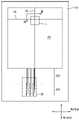
도 4는 도 1의 Ⅳ 부분을 확대한 도면이고, 도 5는 본 발명의 또 다른 실시예에 따른 데드영역을 나타낸 도면이다. 도 6은 도 4 및 도 5의 Ⅵ-Ⅵ선을 따라 취한 단면도이고, 도 7은 도 4 및 도 5의 Ⅶ-Ⅶ선을 따라 취한 단면도이며, 도 8은 도 4 및 도 5의 Ⅷ-Ⅷ선을 따라 취한 단면도이다.4 is an enlarged view of part IV of FIG. 1, and FIG. 5 is a view showing a dead area according to another embodiment of the present invention. 6 is a cross-sectional view taken along line VI-VI of FIGS. 4 and 5, FIG. 7 is a cross-sectional view taken along line VII-VII of FIGS. 4 and 5, and FIG. 8 is a cross-sectional view taken along line VIII-VIII of FIGS. 4 and 5. This is a cross section taken along the line.
도 4 및 도 6을 참조하면, 팬아웃부(200)는 제1배선들(210) 및 제2배선들(220)을 포함하고, 패드부(300)는 제1패드들(311) 및 제2패드들(312)을 포함한다. 제1배선들(210) 및 제2배선들(220)은 제1방향을 따라 연장되며, 서로 인접하게 배치된다. 제1배선들(210) 및 제2배선들(220)은 서로 교번적으로 배열될 수 있다. 예컨대, 제1배선들(210) 및 제2배선들(220)은 제2방향을 따라 서로 교번적으로 배치되며, 서로 다른 층에 위치할 수 있다.4 and 6, the fan-out
일 실시예에 따르면, 제1배선들(210) 각각은 게이트절연층(103)과 제1절연층(105) 사이, 예컨대 제1 및 제2박막트랜지스터(120, 130)의 게이트전극(122, 132) 및/또는 스토리지 커패시터(140)의 제1전극(141)과 동일한 층에 위치할 수 있다. 제2배선들(220) 각각은 제1절연층(105) 및 제2절연층(106) 사이, 예컨대 스토리지 커패시터(140)의 제2전극과 동일한 층에 위치할 수 있다.According to an embodiment, each of the
제1패드들(311) 각각은 제1배선(210)과 연결되고, 제2패드들(312) 각각은 제2배선(220)과 연결된다. 제1패드들(311)과 제2패드들(312)은 액티브영역(AA)으로부터 멀어지는 제1방향을 따라 배열될 수 있다. 예컨대, 제1패드들(311) 및 제2패드들(312)은 제1방향을 따라 서로 교번적으로 배열될 수 있다.Each of the
제1패드들(311) 및 제2패드들(312)은 하나의 열을 이룰 수 있다. 일 실시예에 따르면, 제1패드들(311) 제2패드들(312)은 서로 교번적으로 배열되어 복수의 열들을 이루고, 복수의 열들은 제2방향을 따라 배열될 수 있다. 예를 들어, 도 4에 도시된 바와 같이 2개의 제1패드들(311)과 2개의 제2패드들(312)이 서로 교번적으로 배치되어 하나의 열을 이루고, 이와 같이 형성된 복수의 열들이 제2방향을 따라 배열될 수 있다. 도 4에서는, 하나의 열을 이루는 패드들이 4개인 경우를 설명하였으나 본 발명은 이에 한정되지 않는다. 또 다른 실시예로서, 1개 이상의 제1패드(들) (311) 및 1개 이상의 제2패드(들) (312)이 하나의 열을 이룰 수 있다.The
제1패드들(311) 및 제2패드들(312)은 제2방향을 따라서는 같은 종류끼리 인접하게 배열될 수 있다. 예컨대, 제1패드들(311)은 제2방향을 따라 배열되어 적어도 하나의 행을 이룰 수 있고, 제2패드들(312)은 제2방향을 따라 배열되어 적어도 하나의 행을 이룰 수 있으며, 제1패드들(311)의 행과 제2패드들(312)의 행은 서로 교번적으로 배치되어 복수의 행을 이룰 수 있다.The
서로 인접한 제1배선들(210)과 제2배선들(220)이 다른 층에 형성되어 있고, 제1배선들(210) 및 제2배선들(220)과 연결된 제1패드들(311)과 제2패드들(312)이 오버랩되는 구간(OL1)이 생기도록 제1방향을 따라 서로 교번적으로 배치되므로, 제1폭(W1)을 갖는 좁은 공간에 배선들(210, 220)간의 전기적 단락없이 많은 패드들(311, 312)을 배치할 수 있다. 즉, 고해상도의 표시 장치를 형성할 수 있다.The
도 4에서는 제1방향으로 배열된 제1패드들(311)과 제2패드들(312)이 동일 축 선상에 배치된 경우를 설명하였으나, 본 발명은 이에 제한되지 않는다. 또 다른 실시예에 따르면, 도 5에 도시된 바와 같이 제1패드들(311)과 제2패드들(312)이 제1방향을 따라 서로 교번적으로 배열되되, 오버랩되는 구간(OL2)이 생기도록 제2 방향으로 쉬프트되어 배열될 수 있다.In FIG. 4, the case where the
도 5 및 도 6을 참조하면, 서로 인접한 제1배선들(210)과 제2배선들(220)이 다른 층에 형성되어 있고, 제1배선들(210) 및 제2배선들(220)과 연결된 제1패드들(311)과 제2패드들(312)이 오버랩되는 구간(OL2)이 생기도록 제1방향을 따라 서로 교번적으로 배치되므로, 제1폭(W1)을 갖는 좁은 공간에 배선들(210, 220)간의 전기적 단락없이 많은 패드들(311, 312)을 배치할 수 있다. 즉, 고해상도의 표시 장치를 형성할 수 있다.5 and 6, the
도 7을 참조하면, 제1배선(210)은 게이트절연층(103) 위에 배치되고, 제1패드(311)는 제1절연층(105)을 가운데 개재한 채로 제1배선(210)과 다른 층에 배치된다. 예컨대, 제1패드(311)는 제1절연층(105)을 가운데 개재한 채로 제1배선(210)의 위에 배치될 수 있다. 일 실시예에 따르면, 제1배선(210)은 앞서 도 3을 참조하여 설명한 제1 및 제2박막트랜지스터(120, 130)의 게이트전극(122, 132) 및/또는 스토리지 커패시터(140)의 제1전극(141)과 동일 층에 위치하고, 제1패드(311)는 앞서 도 3을 참조하여 설명한 스토리지 커패시터(140)의 제2전극(142)과 동일 층에 위치할 수 있다.Referring to FIG. 7 , the
제1패드(311)는 아일랜드 타입으로 패터닝되며, 제1배선(210), 예컨대 제1배선(210)의 일 단부와 중첩되게 배치된다. 제1배선(210)과 제1패드(311) 사이에는 제1절연층(105)이 개재되어 있으므로, 제1배선(210)과 제1패드(311)는 전기적으로 절연되어 있다. 제1배선(210) 및 제1패드(311)와 다른 층에 있는 제1연결부(321)에 의해 전기적으로 연결된다.The
제1연결부(321)는 제1배선(210) 및 제1패드(311) 위에 배치되며, 제1연결부(321)와 제1패드(311) 사이에는 제2절연층(106)이 개재된다. 일 실시예에 따르면, 제1연결부(321)는 앞서 도 2 및 도 3을 참조하여 설명한 제1 및 제2박막트랜지스터(120, 130)의 소스전극(123, 133) 및 드레인전극(124, 143), 및/또는 데이터선(DL)과 동일 층에 형성될 수 있다.The
제1연결부(321)의 일부(321a)가 제1배선(210) 및 제1패드(311)에 접촉하여, 제1배선(210)과 제1패드(311)는 전기적으로 연결될 수 있다. 제1연결부(321)의 일부(321a)는 제2절연층(106)에 형성된 제2홀(H2)을 통해 제1패드(311)와 접촉할 수 있고, 제1절연층(105)에 형성된 제1홀(H1)을 통해 제1배선(210)과 접촉할 수 있다.A
제1홀(H1) 및 제2홀(H2)은 서로 중첩하도록 형성되어 제1연결부(321)는 제1배선(210) 및 제1패드(311)와 동시에 접촉할 수 있다. 즉, 제1연결부(321)와 제1배선(210)의 접속지점 및 제1연결부(321)와 제1패드(311)의 접속지점은 서로 중첩될 수 있다. 이 때, 제1연결부(321)의 일부(321a)가 제1배선(210)과 접촉할 수 있도록 제1패드(311)에는 제1홀(H1) 및 제2홀(H2)과 중첩하는 제1관통홀(TH1)이 포함된다.The first hole H1 and the second hole H2 are formed to overlap each other so that the
제2홀(H2)은 제1관통홀(TH1) 보다 크게 형성되어 제1연결부(321)는 제1패드(311)의 측면뿐만 아니라 상부면의 일부와도 접촉할 수 있다.The second hole H2 is formed to be larger than the first through hole TH1 so that the
제1연결부(321) 상에는 평탄화층(107)이 형성될 수 있으며, 평탄화층(107)은 제1연결부(321)와 대응되는 위치에 형성된 개구(OP)를 포함할 수 있다. 개구(OP)를 통해 제1연결부(321)는 외부로 노출될 수 있고, 제1연결부(321) 상에 드라이버 IC(D-IC)가 도전성 볼을 포함하는 접착물질에 의해 제1연결부(321) 상에 본딩될 수 있다.A
도 8을 참조하면, 제2배선(220)은 제1절연층(105) 위에 배치되고, 제2패드(312)는 제1절연층(105)을 가운데 개재한 채로 제2배선(220)과 다른 층에 배치된다. 예컨대, 제2패드(312)는 제1절연층(105)을 가운데 개재한 채로 제2배선(220)의 아래에 배치될 수 있다. 제2배선(220)은 제1패드(311)와 동일 층에 배치될 수 있고, 제2패드(312)는 제1배선(210)과 동일 층에 배치될 수 있다. 일 실시예에 따르면, 제2패드(312)는 앞서 도 3을 참조하여 설명한 제1 및 제2박막트랜지스터(120, 130)의 게이트전극(122, 132) 및/또는 스토리지 커패시터(140)의 제1전극(141)과 동일 층에 위치하고, 제2배선(220)은 앞서 도 3을 참조하여 설명한 스토리지 커패시터(140)의 제2전극(142)과 동일 층에 위치할 수 있다.Referring to FIG. 8 , the
제2패드(312)는 아일랜드 타입으로 패터닝되며, 제2배선(220), 예컨대 제2배선(220)의 일 단부와 중첩되도록 배치된다. 제2배선(220)과 제2패드(312) 사이에는 제1절연층(105)이 개재되어 있으므로, 제2배선(220)과 제2패드(312)는 전기적으로 절연되어 있다. 제2배선(220) 및 제2패드(312)는 다른 층에 있는 제2연결부(322)에 의해 전기적으로 연결된다.The
제2연결부(322)는 제2배선(220) 및 제2패드(312) 위에 배치되며, 제2연결부(322)와 제2배선(220) 사이에는 제2절연층(106)이 개재된다. 제2연결부(322)는 제1연결부(321)와 동일 층에 배치될 수 있다. 일 실시예에 따르면, 제2연결부(322)는 앞서 도 2 및 도 3을 참조하여 설명한 제1 및 제2박막트랜지스터(120, 130)의 소스전극(123, 133) 및 드레인전극(124, 134), 및/또는 데이터선(DL)과 동일 층에 형성될 수 있다.The
제2연결부(322)의 일부(322a)가 제2배선(220) 및 제2패드(312)에 접촉하여, 제2배선(220)과 제2패드(312)는 전기적으로 연결될 수 있다. 제2연결부(322)의 일부(322a)는 제2절연층(106)에 형성된 제4홀(H4)을 통해 제2배선(220)과 접촉할 수 있고, 제1절연층(105)에 형성된 제3홀(H3)을 통해 제2패드(312)와 접촉할 수 있다.A
제3홀(H3) 및 제4홀(H4)은 서로 중첩하도록 형성되어 제2연결부(322)는 제2배선(220) 및 제2패드(312)과 동시에 접촉할 수 있다. 즉, 제2연결부(322)와 제2배선(220)의 접속지점 및 제2연결부(322)와 제2패드(312)의 접속지점은 서로 중첩될 수 있다. 이 때, 제2연결부(322)의 일부(321a)가 제2패드(312)와 접촉할 수 있도록 제12배선에는 제3홀(H3) 및 제4홀(H4)과 중첩하는 제2관통홀(TH2)이 포함될 수 있다.The third hole H3 and the fourth hole H4 are formed to overlap each other so that the
제4홀(H4)은 제2관통홀(TH2) 보다 크게 형성되어 제2연결부(322)는 제2배선(220)의 측면뿐만 아니라 상부면의 일부와도 접촉할 수 있다.The fourth hole H4 is formed to be larger than the second through hole TH2 so that the
제2연결부(322) 상에는 평탄화층(107)이 형성될 수 있으며, 평탄화층(107)은 제2연결부(322)와 대응되는 위치에 형성된 개구(OP)를 포함할 수 있다. 개구(OP)를 통해 제2연결부(322)는 외부로 노출될 수 있고, 제2연결부(322) 상에 드라이버 IC(D-IC)가 도전성 볼을 포함하는 접착물질에 의해 제2연결부(322) 상에 본딩될 수 있다.A
도 7 및 도 8에 도시된 바와 같이, 기판(100)으로부터 제1연결부(321)까지의 높이 및 기판(100)으로부터 제2연결부(322)까지의 높이가 동일하게 형성되므로, 패드부(300)의 높이 차이로 인한 드라이버 IC(D-IC)의 본딩 불량을 방지할 수 있다.As shown in FIGS. 7 and 8 , since the height from the
도시되지는 않았으나, 본 발명의 또 다른 실시예에 따르면, 패드부(300)에 위치하는 제1연결부(321) 및 제2연결부(322) 상에는 도전성 보호층이 더 포함될 수 있다. 비제한적인 실시예로서, 도전성 보호층은, 인듐틴옥사이드(indium tin oxide: ITO), 인듐징크옥사이드(indium zink oxide: IZO), 징크옥사이드(zink oxide: ZnO), 인듐옥사이드(indium oxide: In2O3), 인듐갈륨옥사이드(indium galium oxide: IGO), 및 알루미늄징크옥사이드(aluminium zink oxide: AZO)을 포함하는 그룹에서 선택된 투명 도전성 산화물을 포함할 수 있다. 도전성 보호층은 제1연결부(321) 및 제2연결부(322)의 부식을 방지할 수 있다.Although not shown, according to another embodiment of the present invention, a conductive protective layer may be further included on the
이와 같이 본 발명은 도면에 도시된 일 실시예를 참고로 하여 설명하였으나 이는 예시적인 것에 불과하며 당해 분야에서 통상의 지식을 가진 자라면 이로부터 다양한 변형 및 실시예의 변형이 가능하다는 점을 이해할 것이다. 따라서, 본 발명의 진정한 기술적 보호 범위는 첨부된 특허청구범위의 기술적 사상에 의하여 정해져야 할 것이다.As such, the present invention has been described with reference to one embodiment shown in the drawings, but this is merely exemplary, and those skilled in the art will understand that various modifications and variations of the embodiment are possible therefrom. Therefore, the true technical scope of protection of the present invention should be determined by the technical spirit of the appended claims.
210: 제1팬아웃 배선(제1배선)
220: 제1팬아웃 배선(제2배선)
311: 제1패드
312: 제2패드
321: 제1연결부
322: 제2연결부210: first fan-out wiring (first wiring)
220: first fan-out wiring (second wiring)
311: first pad
312: second pad
321: first connection
322: second connection part
Claims (20)
Translated fromKorean상기 기판의 데드영역 상에 배치된 제1배선;
상기 제1배선과 중첩하는 제1패드;
상기 제1배선과 상기 제1패드를 전기적으로 연결하는 제1연결부;
상기 제1배선과 다른 층에 위치하며, 상기 제1배선과 인접한 제2배선;
상기 제2배선과 중첩하는 제2패드;
상기 제2배선과 상기 제2패드를 전기적으로 연결하는 제2연결부;
상기 제1배선과 상기 제1패드 사이에 위치하고 제1홀을 포함하는 제1절연층; 및
상기 제1패드와 상기 제1연결부 사이에 위치하고 제2홀을 갖는 제2절연층;을 포함하고,
상기 제1패드는 상기 제1패드의 양측 단부 사이에 위치하는 제1관통홀을 포함하고, 상기 제1연결부는 상기 제2홀을 통해 상기 제1패드와 접촉하고 상기 제1관통홀 및 상기 제1홀을 통해 상기 제1배선과 접촉하고,
상기 제1홀, 상기 제2홀, 및 상기 제1관통홀은 서로 중첩하며,
상기 제1홀, 상기 제2홀, 및 상기 제1관통홀의 중첩구조를 중심으로 일측에 위치하는 상기 제1배선과 상기 제1연결부 사이의 수직거리는, 상기 제1홀, 상기 제2홀, 및 상기 제1관통홀의 중첩구조를 중심으로 타측에 위치하는 상기 제1배선과 상기 제1연결부 사이의 수직거리와 동일한, 표시 장치a substrate including an active area on which a plurality of pixels are formed and a dead area adjacent to the active area;
a first wiring disposed on a dead region of the substrate;
a first pad overlapping the first wiring;
a first connection portion electrically connecting the first wire and the first pad;
a second wiring positioned on a different layer from the first wiring and adjacent to the first wiring;
a second pad overlapping the second wiring;
a second connector electrically connecting the second wire and the second pad;
a first insulating layer positioned between the first wiring and the first pad and including a first hole; and
A second insulating layer positioned between the first pad and the first connection portion and having a second hole;
The first pad includes a first through hole positioned between end portions of both sides of the first pad, and the first connection part contacts the first pad through the second hole and connects the first through hole and the first through hole. In contact with the first wiring through one hole,
The first hole, the second hole, and the first through hole overlap each other,
The vertical distance between the first wiring and the first connection part located on one side of the overlapping structure of the first hole, the second hole, and the first through hole is the first hole, the second hole, and A display device that is equal to the vertical distance between the first connection part and the first wiring located on the other side of the overlapping structure of the first through hole.
상기 제1패드와 상기 제2패드는 서로 다른 층에 위치하는, 표시 장치.According to claim 1,
The first pad and the second pad are positioned on different layers.
상기 제1연결부와 상기 제2연결부는 동일한 층에 위치하는, 표시 장치.According to claim 1 or 2,
The first connection part and the second connection part are located on the same layer.
상기 제1배선과 상기 제2패드는 동일한 층에 위치하고, 상기 제2배선과 상기 제1패드는 동일한 층에 위치하는, 표시 장치.According to claim 1,
wherein the first wiring and the second pad are positioned on the same layer, and the second wiring and the first pad are positioned on the same layer.
상기 제1연결부는 상기 제1배선 및 상기 제1패드의 위에 배치되며, 상기 제2연결부는 상기 제2배선 및 상기 제2패드의 위에 배치되는, 표시 장치.According to claim 1,
The first connection part is disposed on the first wire and the first pad, and the second connection part is disposed on the second wire and the second pad.
상기 제1연결부의 일부는 상기 제1배선 및 상기 제1패드와 동시에 접촉하고,
상기 제2연결부의 일부는 상기 제2배선 및 상기 제2패드와 동시에 접촉하는, 표시 장치.According to claim 1,
A portion of the first connection portion contacts the first wire and the first pad at the same time;
A portion of the second connection portion contacts the second wire and the second pad at the same time.
상기 제2홀은 상기 제1관통홀 보다 큰, 표시 장치.According to claim 1,
The second hole is larger than the first through hole.
상기 기판의 데드영역 상에 배치된 제1배선;
상기 제1배선과 중첩하는 제1패드;
상기 제1배선과 상기 제1패드를 전기적으로 연결하는 제1연결부;
상기 제1배선과 다른 층에 위치하며, 상기 제1배선과 인접한 제2배선;
상기 제2배선과 중첩하는 제2패드;
상기 제2배선과 상기 제2패드를 전기적으로 연결하는 제2연결부;
상기 제2패드와 상기 제2배선 사이에 개재되고 제3홀을 포함하는 제1절연층; 및
상기 제2배선과 상기 제2연결부 사이에 개재되고 제4홀을 포함하는 제2절연층;을 포함하고,
상기 제2배선은 제2관통홀을 포함하되, 상기 제2관통홀은 상기 제2패드의 양측 단부 사이에 위치하고, 상기 제2연결부는 상기 제4홀을 통해 상기 제2배선과 접촉하고 상기 제2관통홀 및 상기 제3홀을 통해 상기 제2패드와 접촉하며,
상기 제3홀, 상기 제4홀, 및 상기 제2관통홀은 서로 중첩하고,
상기 제3홀, 상기 제4홀, 및 상기 제2관통홀의 중첩구조를 중심으로 일측에 위치하는 상기 제2패드와 상기 제2연결부 사이의 수직거리는, 상기 제3홀, 상기 제4홀, 및 상기 제2관통홀의 중첩구조를 중심으로 타측에 위치하는 상기 제2패드와 상기 제2연결부 사이의 수직거리와 동일한, 표시 장치.a substrate including an active area on which a plurality of pixels are formed and a dead area adjacent to the active area;
a first wiring disposed on a dead region of the substrate;
a first pad overlapping the first wiring;
a first connection portion electrically connecting the first wire and the first pad;
a second wiring positioned on a different layer from the first wiring and adjacent to the first wiring;
a second pad overlapping the second wiring;
a second connector electrically connecting the second wire and the second pad;
a first insulating layer interposed between the second pad and the second wire and including a third hole; and
A second insulating layer interposed between the second wiring and the second connection portion and including a fourth hole;
The second wire includes a second through hole, the second through hole is located between both ends of the second pad, and the second connection part contacts the second wire through the fourth hole and Contacting the second pad through the second through hole and the third hole;
The third hole, the fourth hole, and the second through hole overlap each other,
The vertical distance between the second pad and the second connection part located on one side of the overlapping structure of the third hole, the fourth hole, and the second through hole is the third hole, the fourth hole, and A display device that is equal to a vertical distance between the second pad and the second connecting portion located on the other side of the overlapping structure of the second through holes.
상기 제4홀은 상기 제2관통홀 보다 큰, 표시 장치.According to claim 11,
The fourth hole is larger than the second through hole.
상기 액티브영역에 위치하며, 활성층, 게이트전극, 소스전극 및 드레인전극을 포함하는 박막트랜지스터; 및
상기 액티브영역에 위치하며, 제1전극 및 상기 제1전극 위에 위치하는 제2전극을 포함하는 스토리지 커패시터;를 더 포함하는, 표시 장치.According to claim 1 or 11,
a thin film transistor positioned in the active region and including an active layer, a gate electrode, a source electrode, and a drain electrode; and
The display device further includes a storage capacitor positioned in the active area and including a first electrode and a second electrode positioned on the first electrode.
상기 제1배선 및 상기 제2패드는, 상기 게이트전극 및 상기 제1전극과 동일층에 위치하는, 표시 장치.According to claim 14,
The first wiring and the second pad are positioned on the same layer as the gate electrode and the first electrode.
상기 제2배선 및 상기 제1패드는 상기 제2전극과 동일층에 위치하는, 표시 장치.According to claim 14,
The second wiring and the first pad are positioned on the same layer as the second electrode.
상기 제1배선 및 상기 제2배선은 상기 액티브영역을 지나는 신호선들과 연결되는, 표시 장치.According to claim 1 or 11,
The first wire and the second wire are connected to signal lines passing through the active area.
상기 제1패드 및 상기 제2패드는 상기 액티브영역으로부터 멀어지는 제1방향을 따라 배열된, 표시 장치.According to claim 1 or 11,
The first pad and the second pad are arranged along a first direction away from the active area.
복수의 상기 제1패드들과 복수의 상기 제2패드들은 상기 제1방향을 따라 서로 교번적으로 배열된, 표시 장치.According to claim 18,
A plurality of first pads and a plurality of second pads are alternately arranged along the first direction.
복수의 상기 제1배선들과 복수의 상기 제2배선들은 서로 교번적으로 배열된, 표시 장치.According to claim 1 or 11,
The plurality of first wires and the plurality of second wires are alternately arranged with each other.
Priority Applications (2)
| Application Number | Priority Date | Filing Date | Title |
|---|---|---|---|
| KR1020150098408AKR102490884B1 (en) | 2015-07-10 | 2015-07-10 | Display device |
| US15/019,825US9954009B2 (en) | 2015-07-10 | 2016-02-09 | Display device |
Applications Claiming Priority (1)
| Application Number | Priority Date | Filing Date | Title |
|---|---|---|---|
| KR1020150098408AKR102490884B1 (en) | 2015-07-10 | 2015-07-10 | Display device |
Publications (2)
| Publication Number | Publication Date |
|---|---|
| KR20170007649A KR20170007649A (en) | 2017-01-19 |
| KR102490884B1true KR102490884B1 (en) | 2023-01-25 |
Family
ID=57731590
Family Applications (1)
| Application Number | Title | Priority Date | Filing Date |
|---|---|---|---|
| KR1020150098408AActiveKR102490884B1 (en) | 2015-07-10 | 2015-07-10 | Display device |
Country Status (2)
| Country | Link |
|---|---|
| US (1) | US9954009B2 (en) |
| KR (1) | KR102490884B1 (en) |
Families Citing this family (7)
| Publication number | Priority date | Publication date | Assignee | Title |
|---|---|---|---|---|
| CN104898887B (en)* | 2015-06-23 | 2017-10-17 | 京东方科技集团股份有限公司 | A kind of built-in type touch display screen, its driving method and display device |
| KR102373441B1 (en) | 2017-03-31 | 2022-03-14 | 삼성디스플레이 주식회사 | Display apparatus |
| KR102652448B1 (en)* | 2018-03-13 | 2024-03-29 | 삼성디스플레이 주식회사 | Display apparatus |
| CN109521611B (en)* | 2018-12-20 | 2021-06-18 | 上海中航光电子有限公司 | Display panels and display devices |
| KR20210131508A (en) | 2020-04-23 | 2021-11-03 | 삼성디스플레이 주식회사 | Display Apparatus |
| KR20220016407A (en) | 2020-07-31 | 2022-02-09 | 삼성디스플레이 주식회사 | Display apparatus |
| US11848333B2 (en)* | 2021-08-24 | 2023-12-19 | Innolux Corporation | Electronic device |
Family Cites Families (11)
| Publication number | Priority date | Publication date | Assignee | Title |
|---|---|---|---|---|
| KR100858297B1 (en) | 2001-11-02 | 2008-09-11 | 삼성전자주식회사 | Reflective-transmissive type liquid crystal display device and method of manufacturing the same |
| KR100450701B1 (en)* | 2001-12-28 | 2004-10-01 | 엘지.필립스 엘시디 주식회사 | The substrate for LCD and method for fabricating the same |
| KR100417916B1 (en)* | 2001-12-29 | 2004-02-14 | 엘지.필립스 엘시디 주식회사 | Array Panel for Liquid Crystal Display Device |
| KR100943283B1 (en) | 2003-06-30 | 2010-02-23 | 엘지디스플레이 주식회사 | LCD Display |
| KR100776480B1 (en) | 2005-08-30 | 2007-11-16 | 삼성에스디아이 주식회사 | OLED display and manufacturing method thereof |
| KR101318217B1 (en)* | 2006-09-29 | 2013-10-16 | 엘지디스플레이 주식회사 | Liquid crystal Display device and method for fabricating of the same |
| TWI441198B (en)* | 2011-12-30 | 2014-06-11 | Au Optronics Corp | Panel and its method |
| KR102025835B1 (en) | 2012-11-26 | 2019-11-27 | 삼성디스플레이 주식회사 | Display apparatus and organic luminescense display apparatus |
| KR101978789B1 (en) | 2012-12-24 | 2019-05-15 | 엘지디스플레이 주식회사 | Array substrate for display device and method of fabricating the same |
| KR101942850B1 (en) | 2013-02-27 | 2019-04-17 | 엘지디스플레이 주식회사 | Liquid crystal display and method of fabricating the same |
| KR102117109B1 (en)* | 2013-10-22 | 2020-06-01 | 삼성디스플레이 주식회사 | Organic light-emitting display apparatus |
- 2015
- 2015-07-10KRKR1020150098408Apatent/KR102490884B1/enactiveActive
- 2016
- 2016-02-09USUS15/019,825patent/US9954009B2/enactiveActive
Also Published As
| Publication number | Publication date |
|---|---|
| US9954009B2 (en) | 2018-04-24 |
| KR20170007649A (en) | 2017-01-19 |
| US20170012056A1 (en) | 2017-01-12 |
Similar Documents
| Publication | Publication Date | Title |
|---|---|---|
| KR102490884B1 (en) | Display device | |
| TWI738058B (en) | Display device and array substrate | |
| US12200993B2 (en) | Display device | |
| US8907327B2 (en) | Display device and organic light-emitting display device having connection part for electronically connecting different levels of conductors | |
| US8975761B2 (en) | Organic light-emitting display comprising a substrate having a fan-out unit configured to connect a display region with a pad unit | |
| JP3990374B2 (en) | Organic electroluminescence display | |
| TWI719570B (en) | Display device | |
| KR102839567B1 (en) | Display device | |
| TW201424471A (en) | Display device and method of manufacturing the same | |
| US9893087B2 (en) | Thin film transistor substrate, display apparatus including thin film transistor substrate, method of manufacturing thin film transistor substrate, and method of manufacturing display apparatus | |
| CN112419908A (en) | Display device and semiconductor device | |
| KR20210107960A (en) | Display panel | |
| CN115701248A (en) | display device | |
| KR102182538B1 (en) | Display apparatus and organic luminescense display apparatus | |
| CN221960993U (en) | Display device | |
| KR20220149841A (en) | Display device | |
| KR102349277B1 (en) | Display apparatus and organic luminescense display apparatus | |
| US12376433B2 (en) | Display device | |
| KR102838085B1 (en) | Display device | |
| US12255194B2 (en) | Display device | |
| US20240072229A1 (en) | Display device | |
| US20220384490A1 (en) | Display device | |
| US20250143125A1 (en) | Display device and display panel | |
| US20250280663A1 (en) | Display Device | |
| KR20240162620A (en) | Display device |
Legal Events
| Date | Code | Title | Description |
|---|---|---|---|
| PA0109 | Patent application | Patent event code:PA01091R01D Comment text:Patent Application Patent event date:20150710 | |
| PG1501 | Laying open of application | ||
| A201 | Request for examination | ||
| PA0201 | Request for examination | Patent event code:PA02012R01D Patent event date:20200708 Comment text:Request for Examination of Application Patent event code:PA02011R01I Patent event date:20150710 Comment text:Patent Application | |
| E902 | Notification of reason for refusal | ||
| PE0902 | Notice of grounds for rejection | Comment text:Notification of reason for refusal Patent event date:20220416 Patent event code:PE09021S01D | |
| E701 | Decision to grant or registration of patent right | ||
| PE0701 | Decision of registration | Patent event code:PE07011S01D Comment text:Decision to Grant Registration Patent event date:20221024 | |
| GRNT | Written decision to grant | ||
| PR0701 | Registration of establishment | Comment text:Registration of Establishment Patent event date:20230117 Patent event code:PR07011E01D | |
| PR1002 | Payment of registration fee | Payment date:20230118 End annual number:3 Start annual number:1 | |
| PG1601 | Publication of registration |