KR102489507B1 - A micro led display and method for manufacturing the same - Google Patents
A micro led display and method for manufacturing the sameDownload PDFInfo
- Publication number
- KR102489507B1 KR102489507B1KR1020200068589AKR20200068589AKR102489507B1KR 102489507 B1KR102489507 B1KR 102489507B1KR 1020200068589 AKR1020200068589 AKR 1020200068589AKR 20200068589 AKR20200068589 AKR 20200068589AKR 102489507 B1KR102489507 B1KR 102489507B1
- Authority
- KR
- South Korea
- Prior art keywords
- electrode
- electrode layer
- layer
- micro led
- micro
- Prior art date
- Legal status (The legal status is an assumption and is not a legal conclusion. Google has not performed a legal analysis and makes no representation as to the accuracy of the status listed.)
- Active
Links
- 238000004519manufacturing processMethods0.000titleclaimsabstractdescription12
- 238000000034methodMethods0.000titledescription18
- 239000000758substrateSubstances0.000claimsabstractdescription31
- 239000012530fluidSubstances0.000claimsdescription30
- 229910052751metalInorganic materials0.000claimsdescription25
- 239000002184metalSubstances0.000claimsdescription25
- 229920002120photoresistant polymerPolymers0.000claimsdescription16
- 238000005530etchingMethods0.000claimsdescription13
- 239000002070nanowireSubstances0.000claimsdescription7
- 230000008878couplingEffects0.000claimsdescription3
- 238000010168coupling processMethods0.000claimsdescription3
- 238000005859coupling reactionMethods0.000claimsdescription3
- 238000000151depositionMethods0.000claimsdescription3
- 238000001035dryingMethods0.000claimsdescription3
- 238000009713electroplatingMethods0.000claimsdescription2
- 239000011248coating agentSubstances0.000claims1
- 238000000576coating methodMethods0.000claims1
- 230000005684electric fieldEffects0.000description23
- 239000010408filmSubstances0.000description10
- 230000008569processEffects0.000description9
- 230000015572biosynthetic processEffects0.000description7
- 230000000694effectsEffects0.000description7
- 239000003990capacitorSubstances0.000description6
- XLOMVQKBTHCTTD-UHFFFAOYSA-NZinc monoxideChemical compound[Zn]=OXLOMVQKBTHCTTD-UHFFFAOYSA-N0.000description4
- 238000003860storageMethods0.000description4
- CSCPPACGZOOCGX-UHFFFAOYSA-NAcetoneChemical compoundCC(C)=OCSCPPACGZOOCGX-UHFFFAOYSA-N0.000description3
- KFZMGEQAYNKOFK-UHFFFAOYSA-NIsopropanolChemical compoundCC(C)OKFZMGEQAYNKOFK-UHFFFAOYSA-N0.000description3
- YXFVVABEGXRONW-UHFFFAOYSA-NTolueneChemical compoundCC1=CC=CC=C1YXFVVABEGXRONW-UHFFFAOYSA-N0.000description3
- 238000006243chemical reactionMethods0.000description3
- 239000003086colorantSubstances0.000description3
- 238000010586diagramMethods0.000description3
- 230000014509gene expressionEffects0.000description3
- 230000010354integrationEffects0.000description3
- 238000000059patterningMethods0.000description3
- 239000010949copperSubstances0.000description2
- 230000017525heat dissipationEffects0.000description2
- 239000011810insulating materialSubstances0.000description2
- 238000009413insulationMethods0.000description2
- 239000007788liquidSubstances0.000description2
- 238000012986modificationMethods0.000description2
- 230000004048modificationEffects0.000description2
- 239000011368organic materialSubstances0.000description2
- 230000003071parasitic effectEffects0.000description2
- 239000002096quantum dotSubstances0.000description2
- 230000004044responseEffects0.000description2
- 238000004088simulationMethods0.000description2
- 239000011787zinc oxideSubstances0.000description2
- RYGMFSIKBFXOCR-UHFFFAOYSA-NCopperChemical compound[Cu]RYGMFSIKBFXOCR-UHFFFAOYSA-N0.000description1
- GYHNNYVSQQEPJS-UHFFFAOYSA-NGalliumChemical compound[Ga]GYHNNYVSQQEPJS-UHFFFAOYSA-N0.000description1
- 229910052782aluminiumInorganic materials0.000description1
- XAGFODPZIPBFFR-UHFFFAOYSA-NaluminiumChemical compound[Al]XAGFODPZIPBFFR-UHFFFAOYSA-N0.000description1
- -1aluminum (Al)Chemical class0.000description1
- 229910021417amorphous siliconInorganic materials0.000description1
- 229910052802copperInorganic materials0.000description1
- 229910021419crystalline siliconInorganic materials0.000description1
- 230000008021depositionEffects0.000description1
- 238000004070electrodepositionMethods0.000description1
- 238000001962electrophoresisMethods0.000description1
- 238000001652electrophoretic depositionMethods0.000description1
- 238000005516engineering processMethods0.000description1
- 229910052733galliumInorganic materials0.000description1
- 239000007943implantSubstances0.000description1
- 229910052738indiumInorganic materials0.000description1
- APFVFJFRJDLVQX-UHFFFAOYSA-Nindium atomChemical compound[In]APFVFJFRJDLVQX-UHFFFAOYSA-N0.000description1
- 229910010272inorganic materialInorganic materials0.000description1
- 239000011147inorganic materialSubstances0.000description1
- 239000000463materialSubstances0.000description1
- 239000011159matrix materialSubstances0.000description1
- 150000002739metalsChemical class0.000description1
- 150000004767nitridesChemical class0.000description1
- 230000000737periodic effectEffects0.000description1
- 229910021420polycrystalline siliconInorganic materials0.000description1
- 230000000191radiation effectEffects0.000description1
- 229910052715tantalumInorganic materials0.000description1
- GUVRBAGPIYLISA-UHFFFAOYSA-Ntantalum atomChemical compound[Ta]GUVRBAGPIYLISA-UHFFFAOYSA-N0.000description1
- 239000010409thin filmSubstances0.000description1
- XLYOFNOQVPJJNP-UHFFFAOYSA-NwaterSubstancesOXLYOFNOQVPJJNP-UHFFFAOYSA-N0.000description1
- YVTHLONGBIQYBO-UHFFFAOYSA-Nzinc indium(3+) oxygen(2-)Chemical compound[O--].[Zn++].[In+3]YVTHLONGBIQYBO-UHFFFAOYSA-N0.000description1
Images


Classifications
- H—ELECTRICITY
- H10—SEMICONDUCTOR DEVICES; ELECTRIC SOLID-STATE DEVICES NOT OTHERWISE PROVIDED FOR
- H10H—INORGANIC LIGHT-EMITTING SEMICONDUCTOR DEVICES HAVING POTENTIAL BARRIERS
- H10H29/00—Integrated devices, or assemblies of multiple devices, comprising at least one light-emitting semiconductor element covered by group H10H20/00
- H10H29/10—Integrated devices comprising at least one light-emitting semiconductor component covered by group H10H20/00
- H10H29/14—Integrated devices comprising at least one light-emitting semiconductor component covered by group H10H20/00 comprising multiple light-emitting semiconductor components
- H10H29/142—Two-dimensional arrangements, e.g. asymmetric LED layout
- H01L27/156—
- G—PHYSICS
- G09—EDUCATION; CRYPTOGRAPHY; DISPLAY; ADVERTISING; SEALS
- G09F—DISPLAYING; ADVERTISING; SIGNS; LABELS OR NAME-PLATES; SEALS
- G09F9/00—Indicating arrangements for variable information in which the information is built-up on a support by selection or combination of individual elements
- G09F9/30—Indicating arrangements for variable information in which the information is built-up on a support by selection or combination of individual elements in which the desired character or characters are formed by combining individual elements
- G09F9/33—Indicating arrangements for variable information in which the information is built-up on a support by selection or combination of individual elements in which the desired character or characters are formed by combining individual elements being semiconductor devices, e.g. diodes
- G—PHYSICS
- G09—EDUCATION; CRYPTOGRAPHY; DISPLAY; ADVERTISING; SEALS
- G09G—ARRANGEMENTS OR CIRCUITS FOR CONTROL OF INDICATING DEVICES USING STATIC MEANS TO PRESENT VARIABLE INFORMATION
- G09G3/00—Control arrangements or circuits, of interest only in connection with visual indicators other than cathode-ray tubes
- G09G3/20—Control arrangements or circuits, of interest only in connection with visual indicators other than cathode-ray tubes for presentation of an assembly of a number of characters, e.g. a page, by composing the assembly by combination of individual elements arranged in a matrix no fixed position being assigned to or needed to be assigned to the individual characters or partial characters
- G09G3/22—Control arrangements or circuits, of interest only in connection with visual indicators other than cathode-ray tubes for presentation of an assembly of a number of characters, e.g. a page, by composing the assembly by combination of individual elements arranged in a matrix no fixed position being assigned to or needed to be assigned to the individual characters or partial characters using controlled light sources
- G09G3/30—Control arrangements or circuits, of interest only in connection with visual indicators other than cathode-ray tubes for presentation of an assembly of a number of characters, e.g. a page, by composing the assembly by combination of individual elements arranged in a matrix no fixed position being assigned to or needed to be assigned to the individual characters or partial characters using controlled light sources using electroluminescent panels
- G09G3/32—Control arrangements or circuits, of interest only in connection with visual indicators other than cathode-ray tubes for presentation of an assembly of a number of characters, e.g. a page, by composing the assembly by combination of individual elements arranged in a matrix no fixed position being assigned to or needed to be assigned to the individual characters or partial characters using controlled light sources using electroluminescent panels semiconductive, e.g. using light-emitting diodes [LED]
- H—ELECTRICITY
- H10—SEMICONDUCTOR DEVICES; ELECTRIC SOLID-STATE DEVICES NOT OTHERWISE PROVIDED FOR
- H10D—INORGANIC ELECTRIC SEMICONDUCTOR DEVICES
- H10D86/00—Integrated devices formed in or on insulating or conducting substrates, e.g. formed in silicon-on-insulator [SOI] substrates or on stainless steel or glass substrates
- H10D86/40—Integrated devices formed in or on insulating or conducting substrates, e.g. formed in silicon-on-insulator [SOI] substrates or on stainless steel or glass substrates characterised by multiple TFTs
- H10D86/471—Integrated devices formed in or on insulating or conducting substrates, e.g. formed in silicon-on-insulator [SOI] substrates or on stainless steel or glass substrates characterised by multiple TFTs having different architectures, e.g. having both top-gate and bottom-gate TFTs
- H—ELECTRICITY
- H10—SEMICONDUCTOR DEVICES; ELECTRIC SOLID-STATE DEVICES NOT OTHERWISE PROVIDED FOR
- H10H—INORGANIC LIGHT-EMITTING SEMICONDUCTOR DEVICES HAVING POTENTIAL BARRIERS
- H10H20/00—Individual inorganic light-emitting semiconductor devices having potential barriers, e.g. light-emitting diodes [LED]
- H10H20/01—Manufacture or treatment
Landscapes
- Engineering & Computer Science (AREA)
- Physics & Mathematics (AREA)
- General Physics & Mathematics (AREA)
- Theoretical Computer Science (AREA)
- Computer Hardware Design (AREA)
- Devices For Indicating Variable Information By Combining Individual Elements (AREA)
Abstract
Translated fromKorean
Description
Translated fromKorean본 발명은 마이크로 LED 디스플레이에 관한 것으로, 특히, 마이크로 LED 또는 나노 LED와 트랜지스터가 배치된 마이크로 LED 디스플레이 및 그 제조 방법에 관한 것이다.The present invention relates to a micro LED display, and more particularly, to a micro LED display in which a micro LED or nano LED and a transistor are disposed, and a manufacturing method thereof.
최근 이상적인 디스플레이 소자로 마이크로 LED가 부각되고 있다.Recently, micro LED has emerged as an ideal display device.
마이크로 LED 디스플레이는 자발광 특성을 가지는데, 동일하게 자발광 특성을 갖는 OLED와 비교할 때 반응 속도, 밝기, 색재현성 및 저전력 구동특성 측면에서 더 우수하다. 마이크로 LED 디스플레이는 무기물 소자 특성상 높은 내구성과 수명을 가지고 있어 모바일 디스플레이에의 적용에 보다 유리하다.Micro LED displays have self-luminous properties, and are superior in terms of response speed, brightness, color reproducibility, and low-power driving characteristics compared to OLEDs having the same self-luminous properties. Micro LED display has high durability and lifespan due to the characteristics of inorganic elements, so it is more advantageous for application to mobile displays.
마이크로 LED 특성상 모듈 형식으로 조립이 가능하여 초고화질 대형 디스플레이에도 응용이 가능하다.Due to the nature of micro LED, it can be assembled in a module format, so it can be applied to ultra-high-definition large displays.
또한, 마이크로 LED 디스플레이는 플렉서블 디스플레이로 구현이 가능하다.In addition, the micro LED display can be implemented as a flexible display.
마이크로 LED는 RGB 화소 위치에 LED를 직접 이식(전사)하는 방식으로 제조되고 있다.Micro LEDs are manufactured by directly implanting (transferring) LEDs to RGB pixel positions.
마이크로 LED의 상용화 관점에서는 대량전사 가능성과 더불어 생산성, 공정비용, 전사성공률, 대면적공정, 고집적, 그리고 백플레인(backplane)과의 결합호환성이 검증이 되야 한다. 하지만, 종래의 전사공정방식의 경우 상용화 관점에서는 근본적인 한계를 지닌다.From the viewpoint of commercialization of micro LED, productivity, process cost, transfer success rate, large-area process, high integration, and backplane compatibility should be verified along with the possibility of mass transfer. However, in the case of the conventional transfer process method, it has fundamental limitations in terms of commercialization.
마이크로 LED의 경우에는 3~100㎛의 크기를 가지는 소자에 대해서는 물리적인 접촉방식을 통하여 원하는 위치로 대량으로 이식하여야 한다. 하지만, 마이크로 LED의 소자 크기가 더 작아질수록 물리적 접촉방식을 사용하여 이식하는 것은 매우 어렵다.In the case of micro LEDs, a large amount of devices having a size of 3 to 100 μm must be implanted in a desired location through a physical contact method. However, as the device size of the micro LED gets smaller, it is very difficult to implant it using a physical contact method.
특히, 전사공정의 경우에는 >2000ppi (pixel per inch)의 마이크로 LED 집적도 달성은 거의 불가능한 것으로 여겨지고 있다.In particular, in the case of the transfer process, achieving micro LED integration of >2000 ppi (pixel per inch) is considered almost impossible.
대안으로 개별전사 공정없이 Si-CMOS 백플레인칩과 직접 결합하는 μLEDoS (micro LED on Si)방식이 고려되고 있다. 이와 같은 무전사방식의 경우, 청색 마이크로 LED와 Si CMOS를 결합하고 풀컬러 디스플레이를 위해 양자점 기반의 색변환층을 사용하려고 한다. 하지만, 색변환층의 도입으로 인하여 마이크로 LED의 장점을 살리지 못할 뿐 아니라 추가적인 양자점 색변환층의 개발이 필요한 문제점이 있다.As an alternative, µLEDoS (micro LED on Si) method, which is directly coupled to the Si-CMOS backplane chip without an individual transfer process, is being considered. In the case of such a non-transfer method, a blue micro LED and Si CMOS are combined and a quantum dot-based color conversion layer is intended to be used for a full-color display. However, due to the introduction of the color conversion layer, the advantages of the micro LED cannot be utilized, and there is a problem in that an additional quantum dot color conversion layer needs to be developed.
따라서 종래의 전사 방식의 단점을 극복하면서 고집적도 달성이 가능한 새로운 방식의 어셈블리 기술 개발이 매우 시급하다.Therefore, it is very urgent to develop a new assembly technology capable of achieving high integration while overcoming the disadvantages of the conventional transfer method.
본 발명이 이루고자 하는 기술적인 과제는 고정 전극을 이용하여, 마이크로 LED 또는 나노 LED와 트랜지스터가 전기적으로 접속되는 마이크로 LED 디스플레이를 제공하는 것이다.A technical problem to be achieved by the present invention is to provide a micro LED display in which a micro LED or nano LED and a transistor are electrically connected by using a fixed electrode.
또한 본 발명이 이루고자 하는 기술적인 과제는 LED가 기판 표면으로부터 이격 배치되어 방열 효과를 확보하고, 고정 전극을 이용함에 따라 넓은 접촉 면적을 확보할 수 있는 마이크로 LED 디스플레이를 제공하는 것이다.In addition, a technical problem to be achieved by the present invention is to provide a micro LED display capable of ensuring a heat dissipation effect by disposing LEDs spaced apart from a substrate surface and securing a wide contact area by using a fixed electrode.
본 발명의 목적들은 이상에서 언급한 목적으로 제한되지 않으며, 언급되지 않은 본 발명의 다른 목적 및 장점들은 하기의 설명에 의해서 이해될 수 있고, 본 발명의 실시예에 의해 보다 분명하게 이해될 것이다. 또한, 본 발명의 목적 및 장점들은 특허 청구 범위에 나타낸 수단 및 그 조합에 의해 실현될 수 있음을 쉽게 알 수 있을 것이다.The objects of the present invention are not limited to the above-mentioned objects, and other objects and advantages of the present invention not mentioned above can be understood by the following description and will be more clearly understood by the examples of the present invention. It will also be readily apparent that the objects and advantages of the present invention may be realized by means of the instrumentalities and combinations indicated in the claims.
본 발명의 실시예에 따른 마이크로 LED 디스플레이는 기판 상에 배치되며, 게이트 전극, 게이트 절연막, 활성층, 소스 전극 및 드레인 전극을 포함하는 트랜지스터; 상기 트랜지스터의 소스 전극 및 드레인 전극 중 어느 하나로부터 연장되는 제1 전극층과, 상기 제1 전극층과 수평적으로 이격되도록 상기 기판 상에 배치된 제2 전극층; 상기 제1 전극층으로부터 상부 방향으로 연장되는 제1 고정 전극과 상기 제2 전극층으로부터 상부 방향으로 연장되는 제2 고정 전극; 및 상기 제1 고정 전극 및 제2 고정 전극에 양단이 결합되는 LED;를 포함한다.A micro LED display according to an embodiment of the present invention is disposed on a substrate and includes a transistor including a gate electrode, a gate insulating film, an active layer, a source electrode, and a drain electrode; a first electrode layer extending from any one of the source electrode and the drain electrode of the transistor, and a second electrode layer disposed on the substrate to be horizontally spaced apart from the first electrode layer; a first fixed electrode extending upwardly from the first electrode layer and a second fixed electrode extending upwardly from the second electrode layer; and an LED having both ends coupled to the first fixed electrode and the second fixed electrode.
상기 트랜지스터는 바텀 게이트-탑 콘택트(bottom gate-top contact), 바텀 게이트-바텀 콘택트(bottom gate-bottom contact), 톱 게이트-탑 콘택트(top gate-top contact), 톱 게이트-바텀 콘택트(top gate-bottom contact) 중 어느 하나일 수 있다.The transistor includes a bottom gate-top contact, a bottom gate-bottom contact, a top gate-top contact, and a top gate-bottom contact. -bottom contact).
상기 제1 전극층과 제2 전극층 사이에 갭 영역을 포함하고, 상기 갭 영역의 일부 영역에 중첩되는 마이크로 LED 배열 영역을 포함할 수 있다.A gap region may be included between the first electrode layer and the second electrode layer, and a micro LED array region overlapping a partial region of the gap region.
상기 제1 전극층과 상기 제2 전극층은 서로를 향해 돌출되도록 배치될 수 있다.The first electrode layer and the second electrode layer may be disposed to protrude toward each other.
상기 제1 전극층 및 제2 전극층에 양단이 결합되는 LED는 제1 전극층 상부면 및 제2 전극층 상부면으로부터 이격 배치될 수 있다.The LED having both ends coupled to the first electrode layer and the second electrode layer may be spaced apart from the upper surface of the first electrode layer and the upper surface of the second electrode layer.
상기 LED는 1 ~ 100㎛의 길이를 갖는 나노와이어 형태일 수 있다.The LED may be in the form of a nanowire having a length of 1 to 100 μm.
상기 제2 전극층은 전원 전압 라인(VDD) 또는 기저 전압 라인(Vss)에 연결될 수 있다.The second electrode layer may be connected to a power supply voltage line (VDD ) or a ground voltage line (Vss).
본 발명의 실시예에 따른 마이크로 LED 디스플레이의 제조 방법은 (a) 기판 상에 게이트 전극, 게이트 절연막, 활성층, 소스 및 드레인 전극용 금속층을 포함하는 트랜지스터를 형성하고, 상기 트랜지스터의 소스 및 드레인 전극용 금속층으로부터 연장되는 제1 전극층과, 상기 제1 전극층과 수평적으로 갭 영역을 두고 이격되도록 상기 기판 상에 제2 전극층을 형성하는 단계; (b) 상기 제1 전극층과 제2 전극층 사이의 갭 영역을 전체적으로 덮되, 상기 갭 영역 상의 일부 영역에 트렌치 구조의 마이크로 LED 배열 영역이 형성되도록 절연층을 형성하는 단계; (c) 상기 기판 상에 LED가 포함된 유체를 공급하면서 상기 제1 전극층과 제2 전극층에 전기 신호를 인가하여 상기 LED를 상기 트렌치 구조의 마이크로 LED 배열 영역에 배열하는 단계; (d) 상기 절연층 중에서 상기 LED의 양단의 아래 부분을 제거하는 단계; (e) 상기 절연층이 제거된 영역에 상기 제1 전극층으로부터 상부 방향으로 연장되는 제1 고정 전극과 상기 제2 전극층으로부터 상부 방향으로 연장되는 제2 고정 전극을 형성하는 단계; 및 (f) 상기 LED의 양단을 상기 제1 고정 전극 및 제2 고정 전극에 결합하는 단계;를 포함할 수 있다.A method of manufacturing a micro LED display according to an embodiment of the present invention includes (a) forming a transistor including a gate electrode, a gate insulating film, an active layer, and a metal layer for source and drain electrodes on a substrate, and using the source and drain electrodes of the transistor. forming a first electrode layer extending from the metal layer and a second electrode layer on the substrate horizontally spaced apart from the first electrode layer with a gap area; (b) forming an insulating layer so as to entirely cover the gap region between the first electrode layer and the second electrode layer, and to form a micro LED array region having a trench structure in a partial region on the gap region; (c) arranging the LEDs in the micro LED array area of the trench structure by applying an electrical signal to the first electrode layer and the second electrode layer while supplying a fluid containing the LED on the substrate; (d) removing lower portions of both ends of the LED from among the insulating layer; (e) forming a first fixed electrode extending upwardly from the first electrode layer and a second fixed electrode extending upwardly from the second electrode layer in the region where the insulating layer is removed; and (f) coupling both ends of the LED to the first fixed electrode and the second fixed electrode.
상기 (f) 단계 이후에, 상기 소스 및 드레인 전극용 금속층을 식각하여 소스 전극 및 드레인 전극을 형성할 수 있다.After step (f), the source and drain electrodes may be formed by etching the metal layer for the source and drain electrodes.
상기 절연층을 형성하는 단계는 (b1) 상기 제1 전극층, 상기 제2 전극층 및 상기 갭 영역 상에 상기 절연층을 형성하는 단계; 및 (b2) 상기 절연층 중에서 상기 갭 영역 상의 상기 일부 영역에 대응하는 부분을 부분 식각하여 상기 트렌치 구조의 마이크로 LED 배열 영역을 형성하는 단계;를 포함할 수 있다.The forming of the insulating layer may include (b1) forming the insulating layer on the first electrode layer, the second electrode layer, and the gap region; and (b2) forming a micro LED array region of the trench structure by partially etching a portion of the insulating layer corresponding to the partial region on the gap region.
상기 LED를 상기 트렌치 구조의 마이크로 LED 배열 영역에 배열하는 단계는 복수의 열 중에서, 각 열마다 전기 신호를 순차적으로 인가하되, 적색 LED가 포함된 유체를 공급하면서, 적색 화소에 포함되는 트랜지스터와 연결되는 제1 전극층과, 제2 전극층에 전기 신호를 인가하여, 적색 화소에 포함되는 마이크로 LED 배열 영역에 적색 LED를 배열하고 건조시키며, 녹색 LED가 포함된 유체를 공급하면서, 녹색 화소에 포함되는 트랜지스터와 연결되는 제1 전극층과, 제2 전극층에 전기 신호를 인가하여, 녹색 화소에 포함되는 마이크로 LED 배열 영역에 적색 LED를 배열하고 건조시키며, 청색 LED가 포함된 유체를 공급하면서, 청색 화소에 포함되는 트랜지스터와 연결되는 제1 전극층과, 제2 전극층에 전기 신호를 인가하여, 청색 화소에 포함되는 마이크로 LED 배열 영역에 적색 LED를 배열하고 건조시킬 수 있다.In the step of arranging the LEDs in the micro LED array area of the trench structure, electrical signals are sequentially applied to each column among a plurality of columns, while supplying a fluid containing red LEDs and connecting them to transistors included in red pixels. An electrical signal is applied to the first electrode layer and the second electrode layer to arrange and dry the red LEDs in the micro LED array area included in the red pixel, and while supplying a fluid containing the green LED, the transistor included in the green pixel. Applying an electrical signal to the first electrode layer connected to and the second electrode layer, arranging and drying red LEDs in the micro LED array area included in the green pixel, supplying a fluid containing the blue LED, included in the blue pixel Red LEDs may be arranged and dried in the micro LED array area included in the blue pixel by applying an electric signal to the first electrode layer connected to the transistor and the second electrode layer.
상기 절연층 중에서 LED의 양단의 아래 부분을 제거하는 단계는 (d1) 상기 절연층과 상기 LED 상에 포토레지스트를 도포하는 단계; (d2) 상기 포토레지스트 중에서 상기 LED의 상기 양단에 대응하는 부분을 제거하여 포토레지스트 패턴을 형성하는 단계; 및 (d3) 상기 포토레지스트 패턴을 식각 마스크로 사용하여 상기 절연층 중에서 상기 LED의 상기 양단의 아래 부분을 제거하는 단계;를 포함할 수 있다.The step of removing the lower portion of both ends of the LED from the insulating layer may include (d1) applying photoresist on the insulating layer and the LED; (d2) forming a photoresist pattern by removing portions of the photoresist corresponding to both ends of the LED; and (d3) using the photoresist pattern as an etching mask to remove lower portions of the both ends of the LED from among the insulating layer.
상기 제1 고정 전극과 제2 고정 전극은 상기 절연층이 제거된 영역에 금속을 증착 또는 전기 도금하여 형성될 수 있다.The first fixed electrode and the second fixed electrode may be formed by depositing or electroplating a metal on a region from which the insulating layer is removed.
상기 (f) 단계 이후에, 상기 절연층을 전부 제거하는 단계;를 더 포함할 수 있다.After the step (f), removing the entire insulating layer; may be further included.
본 발명에 따른 마이크로 LED 디스플레이는 트렌치 구조(미세우물 구조)의 마이크로 LED 배열 영역에 수평적으로 이격되어 배치된 제1 전극층, 제2 전극층에 LED의 양단을 결합시킴에 따라, 트랜지스터와 LED를 전기적으로 접속시킬 수 있다.The micro LED display according to the present invention connects both ends of the LED to the first electrode layer and the second electrode layer disposed horizontally spaced apart in the micro LED array area of the trench structure (microwell structure), thereby electrically connecting the transistor and the LED. can be connected to.
또한 본 발명에 따른 마이크로 LED 디스플레이는 LED가 기판 표면으로부터 이격되어 있어 방열 효과를 나타낼 수 있으며, 고정 전극의 적용을 통해 넓은 접촉 면적을 확보하는 효과가 있다.In addition, the micro LED display according to the present invention has an effect of securing a large contact area through the application of a fixed electrode, and can exhibit a heat radiation effect because the LED is spaced apart from the substrate surface.
상술한 효과와 더불어 본 발명의 구체적인 효과는 이하 발명을 실시하기 위한 구체적인 사항을 설명하면서 함께 기술한다.In addition to the effects described above, specific effects of the present invention will be described together while explaining specific details for carrying out the present invention.
도 1은 일반적인 2T-1C 구조의 화소(pixel)의 회로도를 나타낸다.
도 2는 본 발명의 실시예에 따라 제조된 LED 디스플레이의 평면도를 나타낸다.
도 3은 도 2에 도시된 LED 디스플레이를 A-B 방향으로 절단했을 때의 단면도를 나타낸다.
도 4는 본 발명의 실시예에 따라 기판 상에 트랜지스터 형성 단계를 설명하기 위한 단면도이다.
도 5는 본 발명의 실시예에 따라 제1 전극층과 제2 전극층을 형성하는 전극층 형성 단계를 설명하기 위한 단면도이다.
도 6은 본 발명의 실시예에 따라 마이크로 LED 배열 영역을 포함하는 절연층을 형성하는 절연층 형성 단계를 설명하기 위한 단면도이다.
도 7은 본 발명의 실시예에 따라 마이크로 LED 배열 영역을 포함하는 절연층을 형성하는 절연층 형성 단계를 설명하기 위한 평면도이다.
도 8은 본 발명의 다른 실시예에 따라 마이크로 LED 배열 영역을 포함하는 절연층을 형성하는 절연층 형성 단계를 설명하기 위한 평면도이다.
도 9는 본 발명의 실시예에 따라 LED를 배열하는 LED 배열 단계를 설명하기 위한 단면도이다.
도 10은 본 발명의 실시예에 따라 LED가 배열된 화소들을 나타내는 단면도이다.
도 11은 본 발명의 실시예에 따라 LED가 배열된 화소들을 나타내는 평면도이다.
도 12는 전극층들 사이에 발생하는 전기장을 시뮬레이션한 결과이다.
도 13은 RGB 색상에 해당하는 나노 LED을 배열하는 방법을 보여주는 순서도이다.
도 14는 본 발명의 실시예에 따라 LED를 결합하는 LED 결합 단계와 소스 전극과 드레인 전극을 형성하는 전극 형성 단계를 설명하기 위한 단면도이다.
도 15는 본 발명의 실시예에 따라 LED 조립단계, 전극 형성 단계, 전극의 패터닝 및 소자 분리 단계를 나타내는 단면도이다.
1 shows a circuit diagram of a pixel of a general 2T-1C structure.
2 shows a plan view of an LED display manufactured according to an embodiment of the present invention.
Figure 3 shows a cross-sectional view when the LED display shown in Figure 2 is cut in the AB direction.
4 is a cross-sectional view illustrating a step of forming a transistor on a substrate according to an embodiment of the present invention.
5 is a cross-sectional view for explaining an electrode layer forming step of forming a first electrode layer and a second electrode layer according to an embodiment of the present invention.
6 is a cross-sectional view illustrating an insulating layer forming step of forming an insulating layer including a micro LED array region according to an embodiment of the present invention.
7 is a plan view illustrating an insulating layer forming step of forming an insulating layer including a micro LED array region according to an embodiment of the present invention.
8 is a plan view illustrating an insulating layer forming step of forming an insulating layer including a micro LED array region according to another embodiment of the present invention.
9 is a cross-sectional view for explaining an LED arrangement step of arranging LEDs according to an embodiment of the present invention.
10 is a cross-sectional view illustrating pixels in which LEDs are arranged according to an embodiment of the present invention.
11 is a plan view illustrating pixels in which LEDs are arranged according to an exemplary embodiment of the present invention.
12 is a simulation result of an electric field generated between electrode layers.
13 is a flowchart illustrating a method of arranging nano LEDs corresponding to RGB colors.
14 is a cross-sectional view for explaining an LED combining step of combining LEDs and an electrode forming step of forming a source electrode and a drain electrode according to an embodiment of the present invention.
15 is a cross-sectional view showing steps of assembling LEDs, forming electrodes, patterning electrodes, and separating devices according to an embodiment of the present invention.
본 명세서에 개시되어 있는 본 발명의 개념에 따른 실시예들에 대해서 특정한 구조적 또는 기능적 설명들은 단지 본 발명의 개념에 따른 실시예들을 설명하기 위한 목적으로 예시된 것으로서, 본 발명의 개념에 따른 실시예들은 다양한 형태들로 실시될 수 있으며 본 명세서에 설명된 실시예들에 한정되지 않는다.Specific structural or functional descriptions of the embodiments according to the concept of the present invention disclosed in this specification are only illustrated for the purpose of explaining the embodiments according to the concept of the present invention, and the embodiments according to the concept of the present invention may be embodied in many forms and are not limited to the embodiments described herein.
본 발명의 개념에 따른 실시예들은 다양한 변경들을 가할 수 있고 여러 가지 형태들을 가질 수 있으므로 실시예들을 도면에 예시하고 본 명세서에 상세하게 설명하고자 한다. 그러나, 이는 본 발명의 개념에 따른 실시예들을 특정한 개시 형태들에 대해 한정하려는 것이 아니며, 본 발명의 사상 및 기술 범위에 포함되는 모든 변경, 균등물, 또는 대체물을 포함한다.Embodiments according to the concept of the present invention can apply various changes and can have various forms, so the embodiments are illustrated in the drawings and described in detail herein. However, this is not intended to limit the embodiments according to the concept of the present invention to specific disclosed forms, and includes all modifications, equivalents, or substitutes included in the spirit and scope of the present invention.
제1 또는 제2 등의 용어는 다양한 구성 요소들을 설명하는데 사용될 수 있지만, 상기 구성 요소들은 상기 용어들에 의해 한정되어서는 안 된다. 상기 용어들은 하나의 구성 요소를 다른 구성 요소로부터 구별하는 목적으로만, 예컨대 본 발명의 개념에 따른 권리 범위로부터 이탈되지 않은 채, 제1구성요소는 제2구성요소로 명명될 수 있고, 유사하게 제2구성요소는 제1구성요소로도 명명될 수 있다.Terms such as first or second may be used to describe various components, but the components should not be limited by the terms. The above terms are only for the purpose of distinguishing one component from another component, e.g., without departing from the scope of rights according to the concept of the present invention, a first component may be termed a second component, and similarly The second component may also be referred to as the first component.
어떤 구성요소가 다른 구성요소에 "연결되어" 있다거나 "접속되어" 있다고 언급된 때에는, 그 다른 구성요소에 직접적으로 연결되어 있거나 또는 접속되어 있을 수도 있지만, 중간에 다른 구성요소가 존재할 수도 있다고 이해되어야 할 것이다. 반면에, 어떤 구성요소가 다른 구성요소에 "직접 연결되어" 있다거나 "직접 접속되어" 있다고 언급된 때에는, 중간에 다른 구성요소가 존재하지 않는 것으로 이해되어야 할 것이다. 구성요소들 간의 관계를 설명하는 다른 표현들, 즉 "~사이에"와 "바로 ~사이에" 또는 "~에 이웃하는"과 "~에 직접 이웃하는" 등도 마찬가지로 해석되어야 한다.It is understood that when an element is referred to as being "connected" or "connected" to another element, it may be directly connected or connected to the other element, but other elements may exist in the middle. It should be. On the other hand, when an element is referred to as “directly connected” or “directly connected” to another element, it should be understood that no other element exists in the middle. Other expressions describing the relationship between elements, such as "between" and "directly between" or "adjacent to" and "directly adjacent to", etc., should be interpreted similarly.
본 명세서에서 사용한 용어는 단지 특정한 실시예를 설명하기 위해 사용된 것으로, 본 발명을 한정하려는 의도가 아니다. 단수의 표현은 문맥상 명백하게 다르게 뜻하지 않는 한, 복수의 표현을 포함한다. 본 명세서에서, "포함하다" 또는 "가지다" 등의 용어는 설시된 특징, 숫자, 단계, 동작, 구성요소, 부분품 또는 이들을 조합한 것이 존재함을 지정하려는 것이지, 하나 또는 그 이상의 다른 특징들이나 숫자, 단계, 동작, 구성요소, 부분품 또는 이들을 조합한 것들의 존재 또는 부가 가능성을 미리 배제하지 않는 것으로 이해되어야 한다.Terms used in this specification are only used to describe specific embodiments, and are not intended to limit the present invention. Singular expressions include plural expressions unless the context clearly dictates otherwise. In this specification, terms such as "comprise" or "having" are intended to designate that the described feature, number, step, operation, component, part, or combination thereof exists, but one or more other features or numbers However, it should be understood that it does not preclude the presence or addition of steps, operations, components, parts, or combinations thereof.
다르게 정의되지 않는 한, 기술적이거나 과학적인 용어를 포함해서 여기서 사용되는 모든 용어들은 본 발명이 속하는 기술 분야에서 통상의 지식을 가진 자에 의해 일반적으로 이해되는 것과 동일한 의미를 가진다. 일반적으로 사용되는 사전에 정의되어 있는 것과 같은 용어들은 관련 기술의 문맥상 가지는 의미와 일치하는 의미를 갖는 것으로 해석되어야 하며, 본 명세서에서 명백하게 정의하지 않는 한, 이상적이거나 과도하게 형식적인 의미로 해석되지 않는다.Unless defined otherwise, all terms used herein, including technical or scientific terms, have the same meaning as commonly understood by one of ordinary skill in the art to which the present invention belongs. Terms such as those defined in commonly used dictionaries should be interpreted as having a meaning consistent with the meaning in the context of the related art, and unless explicitly defined in this specification, it should not be interpreted in an ideal or excessively formal meaning. don't
이하에서는, 본 발명의 몇몇 실시예에 따른 마이크로 LED 디스플레이 및 그 제조 방법을 설명하도록 한다.Hereinafter, a micro LED display and a manufacturing method thereof according to some embodiments of the present invention will be described.
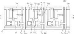
도 1은 일반적인 2T-1C 구조의 화소(pixel)의 회로도를 나타낸다. 도 2는 본 발명의 실시예에 따라 제조된 LED 디스플레이의 평면도를 나타낸다. 도 3은 도 2에 도시된 LED 디스플레이를 A-B 방향으로 절단했을 때의 단면도를 나타낸다.1 shows a circuit diagram of a pixel of a general 2T-1C structure. 2 shows a plan view of an LED display manufactured according to an embodiment of the present invention. Figure 3 shows a cross-sectional view when the LED display shown in Figure 2 is cut in the A-B direction.
도 1은 본 발명에 따라 제조될 수 있는 가장 간단한 구조의 화소의 회로도를 나타낼 뿐 본 발명의 실시예는 이에 한정되지 않는다. 도 3에서는 설명의 편의를 위해 기판(100), 구동 트랜지스터(DT), 전원 전압 라인(VDD) 및 마이크로 LED(ML)을 제외한 부분은 일부 생략하였다.1 shows a circuit diagram of a pixel having the simplest structure that can be manufactured according to the present invention, but the embodiment of the present invention is not limited thereto. In FIG. 3 , parts except for the
도 1 내지 도 3을 참조하면, LED 디스플레이(100)의 하나의 화소는 기판(110)에 형성된 2개의 트랜지스터들(ST, DT), 1개의 커패시터(Cst) 및 마이크로 LED(ML)를 포함할 수 있다.1 to 3, one pixel of the
본 발명에서 트랜지스터는 구동 트랜지스터(DT)를 가리킨다. 트랜지스터에서 제1 전극(161)과 제2 전극(163) 각각은 소스 전극 및 드레인 전극 중 어느 하나일 수 있으며, 본 발명에서는 제1 전극(161)을 소스 전극, 제2 전극(163)을 드레인 전극으로 가정 하에 설명하기로 한다.In the present invention, the transistor refers to the driving transistor DT. In the transistor, each of the
스위칭 트랜지스터(ST)의 게이트 전극은 게이트 라인(GL)에 접속되고, 스위칭 트랜지스터(ST)의 소스 전극은 데이터 라인(DL)에 접속된다. 스위칭 트랜지스터(ST)의 드레인 전극은 구동 트랜지스터(DT)의 게이트 전극과 스토리지 커패시터(Cst)의 제1 단에 접속된다.A gate electrode of the switching transistor ST is connected to the gate line GL, and a source electrode of the switching transistor ST is connected to the data line DL. The drain electrode of the switching transistor ST is connected to the gate electrode of the driving transistor DT and the first terminal of the storage capacitor Cst .
스위칭 트랜지스터(ST)는 게이트 라인(GL)을 통해 공급되는 신호에 응답하여 데이터 라인(DL)과 구동 트랜지스터(DT)의 게이트 전극을 접속시킨다.The switching transistor ST connects the data line DL and the gate electrode of the driving transistor DT in response to a signal supplied through the gate line GL.
구동 트랜지스터(DT)의 게이트 전극(121)은 비아(Via3)를 통해 스위칭 트랜지스터(ST)의 상기 드레인 전극(163)에 접속된다. 구동 트랜지스터(DT)의 소스 전극(161)은 비아(Via1)를 통해 접지(GND)에 접속된다. 구동 트랜지스터(DT)의 드레인 전극(163)은 마이크로 LED(ML)에 접속된다.The
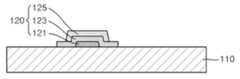
구동 트랜지스터(DT)의 게이트 전극(121) 상에서는 게이트 절연막(123)이 형성된다. 게이트 절연막(123)은 게이트 전극(121)을 감싸는 형태로 형성된다.A
게이트 절연막(123) 상에는 활성층(125)이 형성된다. 활성층(125)은 게이트 절연막(123) 상의 일부 영역에 형성된다.An
구동 트랜지스터(DT)는 스토리지 커패시터(Cst)에 충전된 전압에 대응하는 전류를 전원 전압 라인(VDD)로부터 마이크로 LED(ML)을 통해 접지(GND)로 흐르게 한다.The driving transistor DT causes a current corresponding to the voltage charged in the storage capacitor Cst to flow from the power supply voltage line VDD to the ground GND through the micro LED ML.
스토리지 커패시터(Cst)는 구동 트랜지스터(DT)의 게이트 전극과 접지(GND) 사이에 접속된다.The storage capacitor Cst is connected between the gate electrode of the driving transistor DT and the ground GND.
마이크로 LED(ML)는 구동 트랜지스터(DT)의 드레인 전극(163)과 전원 전압 라인(VDD) 사이에 접속된다. 구체적으로, 마이크로 LED(ML)의 제1 단은 제1 고정 전극(151)을 통해 구동 트랜지스터(DT)의 드레인 전극(163)에 접속된다. 마이크로 LED(ML)의 제2 단은 제2 고정 전극(153)을 통해 전원 전압 라인(VDD)에 접속된다. 이때, 전원 전압 라인(VDD)을 공급하는 라인은 구동 트랜지스터(DT)와 다른 레이어에 형성될 수 있는데, 이 경우 전원 전극(165)과 전원(VDD)이 비아(Via2)를 통해 접속될 수 있다. 또한 제2 전극층(133)은 전원 전압 라인(VDD) 또는 기저 전압 라인(Vss)에 연결된다.The micro LED ML is connected between the
실시예에 따라, 마이크로 LED(ML)는 1 ~ 100㎛의 길이를 갖는 나노와이어 형태일 수 있다. 본 발명에서 나노와이어는 단면의 지름이 대략 10nm ~ 10㎛ 일 수 있다. 또한 나노와이어는 비교적 높은 종횡비(aspect ratio)를 가지며, 종횡비는 대략 1.1 ~ 10 일 수 있다. 종횡비가 높은 나노와이어는 표면적이 넓으므로 에너지 전달 및 성능이 우수하며 투명도가 높은 장점이 있다.Depending on the embodiment, the micro LED (ML) may be in the form of a nanowire having a length of 1 μm to 100 μm. In the present invention, the nanowire may have a cross-sectional diameter of approximately 10 nm to 10 μm. In addition, the nanowire has a relatively high aspect ratio, and the aspect ratio may be approximately 1.1 to 10. Nanowires with a high aspect ratio have a large surface area, so they have excellent energy transfer and performance, and have high transparency.
LED 디스플레이(100)는 도 4 내지 도 13를 통해 설명되는 바와 같이, 트랜지스터 형성 단계, 전극층 형성 단계, 절연층 형성 단계, LED 배열 단계, 고정 전극 형성 단계 및 LED 결합 단계를 통해 제조될 수 있다.As described with reference to FIGS. 4 to 13 , the
도 4는 본 발명의 실시예에 따라 기판 상에 트랜지스터 형성 단계를 설명하기 위한 단면도이다.4 is a cross-sectional view illustrating a step of forming a transistor on a substrate according to an embodiment of the present invention.
도 4를 참조하면, 베이스 회로 형성 단계 동안 기판(110) 상에 베이스 회로(120)를 포함하는 트랜지스터가 형성된다. 여기서 기판은 능동구동 백플레인 혹은 활성화된 매트릭스 백플레인(active matrix backplane)일 수 있다. 상기 트랜지스터는 마이크로 LED의 전류를 조절할 수 있는 트랜지스터이다.Referring to FIG. 4 , a transistor including a
트랜지스터는 활성층(125), 상기 활성층(125)의 온/오프를 담당하는 게이트 전극(121), 직접적으로 전류를 흐르게 하는 소스 전극(161)과 드레인 전극(163), 및 상기 게이트 전극(121)과 활성층(125) 사이에 절연을 위한 게이트 절연막(123)으로 구성된다.The transistor includes an
본 발명의 도면에서는 트랜지스터의 구조를 기판(110) 상에 게이트 전극(121)이 형성되고, 게이트 전극(121)을 감싸는 형태로 게이트 절연막(123)이 형성되며, 게이트 절연막(123) 상에 활성층(125)이 형성되는 구조로 도시하였다.In the drawings of the present invention, the
트랜지스터는 게이트 전극(121)의 위치에 기초하여 역스태거 구조(바텀 게이트형) 및 스태거 구조(톱 게이트형)로 구분된다. 그리고 게이트 전극(121)과 활성층(125)의 배치에 따라 1) 바텀 게이트-탑 콘택트(bottom gate-top contact), 2) 바텀 게이트-바텀 콘택트(bottom gate-bottom contact), 3) 톱 게이트-탑 콘택트(top gate-top contact) 4) 톱 게이트-바텀 콘택트(top gate-bottom contact) 의 4가지 구조로 분류될 수 있다.The transistor is classified into an inverted stagger structure (bottom gate type) and a stagger structure (top gate type) based on the position of the
톱 게이트 구조란, 게이트 절연막(123)의 상측에 게이트 전극(121)이 배치되고, 게이트 절연막(123)의 하측에 활성층(125)이 형성된 형태이다.The top gate structure is a type in which the
바텀 게이트 구조란, 게이트 절연막(123)의 하측에 게이트 전극(121)이 배치되고, 게이트 절연막(123)의 상측에 활성층(125)이 형성된 형태이다.The bottom gate structure is a form in which the
또한, 바텀 콘택트형이란, 소스·드레인 전극(161, 165)이 활성층(125)보다 먼저 형성되어 활성층(125)의 하면이 소스·드레인 전극(161, 165)에 접촉하는 형태이다.In addition, the bottom contact type is a type in which the source and drain
또한, 탑 콘택트형이란, 활성층(125)이 소스·드레인 전극(161, 165)보다 먼저 형성되어 활성층(125)의 상면이 소스·드레인 전극(161, 165)에 접촉하는 형태이다.In addition, the top contact type is a type in which the
본 발명의 트랜지스터는 4가지 구조 중 어느 하나로 적용 가능하다.The transistor of the present invention can be applied in any one of four structures.
게이트 전극(121)은 알루미늄(Al), 구리(Cu), 탄탈륨(Ta) 등의 금속 또는 이들의 금속 질화물 중 적어도 하나의 물질을 포함할 수 있다. 게이트 절연막(123)은 유기 물질, 무기 물질 및/또는 유무기 물질 중 적어도 하나의 물질을 포함할 수 있다. 활성층(125)은 ZnO, IZO(Indium Zinc Oxide), IGZO(Indium Gallium Zinc Oxide), 비정질 실리콘, 다결정 실리콘 및 결정질 실리콘 중 적어도 하나의 물질을 포함할 수 있다.The
도 5는 본 발명의 실시예에 따라 제1 전극층과 제2 전극층을 형성하는 전극층 형성 단계를 설명하기 위한 단면도이다.5 is a cross-sectional view for explaining an electrode layer forming step of forming a first electrode layer and a second electrode layer according to an embodiment of the present invention.
도 5를 참조하면, 베이스 형성 단계 이후 전극층 형성 단계 동안 제1 전극층(131)과 제2 전극층(133)이 형성된다.Referring to FIG. 5 , the
도 5(a)에 도시된 바와 같이, 베이스 회로(120) 상에 베이스 회로(120)를 감싸는 소스 및 드레인 전극용 금속층(130)을 적층하여 형성한다.As shown in FIG. 5(a), the
이후, 도 5(b)에 도시된 바와 같이, 소스 및 드레인 전극용 금속층(130) 중에서 갭 영역(GA)에 대응하는 부분을 제거하여 제1 전극층(131)과 제2 전극층(133)을 형성한다.Then, as shown in FIG. 5 (b), the
일반적으로 디스플레이 회로에서는 트랜지스터와 마이크로 LED가 전극으로 연결되어야 하므로 많은 금속배선을 필요로 한다. 이에 따라 전기장을 통한 마이크로 LED 조립 과정에서 원하지 않는 곳에 기생 전기장(parasitic electric field)이 생길 수 있으므로 이러한 현상을 최소화 하는 것이 중요하다.In general, in a display circuit, a lot of metal wiring is required because transistors and micro LEDs must be connected with electrodes. Accordingly, it is important to minimize this phenomenon because a parasitic electric field may be generated in an undesirable place in the process of assembling the micro LED through the electric field.
이를 위해서 도 5(c)에 도시된 바와 같이, 회로의 모든 소자를 덮고 있도록 전 영역에 전기장 차폐층 역할을 하면서 정렬 역할을 하는 전극을 형성하는 것이 바람직하다. 소스 및 드레인 전극용 금속층(130)을 전 영역에 형성하게 되면, 기생 전기장의 형성을 최소화하면서 동시에 아래에 있는 소자를 전기장으로부터 보호할 수 있다. 도 5(c)는 소스 및 드레인 전극용 금속층(130)이 형성된 후 패턴화된 모습의 평면도로, 제1 전극층(131)과 제2 전극층(133)으로 도시하였다.To this end, as shown in FIG. 5(c), it is preferable to form an electrode that serves as an alignment role while serving as an electric field shielding layer over the entire area so as to cover all elements of the circuit. When the
본 발명에서는 식각을 이용하여, 소스 및 드레인 전극용 금속층(130)으로부터 트랜지스터의 소스 전극(161), 드레인 전극(163), 제1 전극층(131) 및 제2 전극층(133)을 모두 형성할 수 있다.In the present invention, all of the
예를 들어, LED 결합 단계 이후에, 상기 소스 및 드레인 전극용 금속층(130)을 식각하여 소스 전극(161) 및 드레인 전극(163)을 형성할 수 있다.For example, after the LED bonding step, the
실시예에 따라, 제1 금속층(130) 상에 갭 영역(GA)을 제외한 영역에 포토레지스트 패턴을 형성하고 형성된 포토레지스트 패턴을 식각 마스크로 이용해 식각을 수행하여 제1 금속층(130) 중에서 갭 영역(GA) 부분을 제거할 수 있다.According to an embodiment, a photoresist pattern is formed on an area of the
도 5(b), 도 7에 도시된 바와 같이, 갭 영역(GA)은 짧은 너비(D1)와 긴 길이를 갖는 도랑 형태일 수 있다.As shown in FIGS. 5(b) and 7 , the gap area GA may have a trench shape having a short width D1 and a long length.
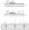
도 6은 본 발명의 실시예에 따라 마이크로 LED 배열 영역을 포함하는 절연층을 형성하는 절연층 형성 단계를 설명하기 위한 단면도이다. 도 7은 본 발명의 실시예에 따라 마이크로 LED 배열 영역을 포함하는 절연층을 형성하는 절연층 형성 단계를 설명하기 위한 평면도이다.6 is a cross-sectional view illustrating an insulating layer forming step of forming an insulating layer including a micro LED array region according to an embodiment of the present invention. 7 is a plan view illustrating an insulating layer forming step of forming an insulating layer including a micro LED array region according to an embodiment of the present invention.
도 6 및 도 7을 참조하면, 전극층 형성 단계 이후 절연층 형성 단계 동안 트렌치 구조의 마이크로 LED 배열 영역(LAA)을 포함하는 절연층(140)이 형성된다.Referring to FIGS. 6 and 7 , during the insulating layer forming step after the electrode layer forming step, the insulating
도 6(a)에 도시된 바와 같이, 제1 전극층(131), 제2 전극층(133) 및 갭 영역(GA) 상에 절연층(140)을 적층하여 형성한다.As shown in FIG. 6(a) , an insulating
이후, 도 6(b)에 도시된 바와 같이, 절연층(140) 중에서 마이크로 LED 배열 영역(LAA)에 대응하는 부분을 부분적으로 제거하여 트렌치(trench) 구조의 마이크로 LED 배열 영역(LAA)을 형성한다. 여기서, 부분적으로 제거하는 것의 의미는 마이크로 LED 배열 영역(LAA)에 대응하는 부분의 절연 물질을 전부 제거하는 것이 아니라 소정의 두께만큼 잔존시킨다는 의미이다.Then, as shown in FIG. 6( b ), a portion of the
예를 들어, 절연층(140) 상에 두께가 서로 다른 포토레지스트를 도포하고 식각을 수행하여 마이크로 LED 배열 영역(LAA)에 대응하는 부분의 절연 물질이 보다 많이 식각되게 하는 방법으로 부분 식각을 수행할 수 있다.For example, partial etching is performed by applying photoresists having different thicknesses on the insulating
다른 예를 들어, 도면에 도시되지는 않았으나, 절연층(140)을 2 이상의 층(레이어)으로 구분하여 적층하고 마이크로 LED 배열 영역(LAA)에 대응하는 부분의 상부층을 제거함으로써 마이크로 LED 배열 영역(LAA)을 형성할 수 있다.For another example, although not shown in the drawing, the insulating
도 7에 도시된 바와 같이, 마이크로 LED 배열 영역(LAA)은 갭 영역(GA)의 일부 영역에 중첩된다. LED 디스플레이(100)는 전체적으로는 다수의 마이크로 LED 배열 영역들(LAA)이 갭 영역(GA)의 길쭉한 방향을 따라 소정의 간격으로 형성될 수 있다.As shown in FIG. 7 , the micro LED array area LAA overlaps a portion of the gap area GA. In the
마이크로 LED 배열 영역(LAA)의 장축 너비(D2)는 갭 영역(GA)의 너비(D1) 보다 길다.The major axis width D2 of the micro LED array area LAA is longer than the width D1 of the gap area GA.
도 8은 본 발명의 다른 실시예에 따라 마이크로 LED 배열 영역을 포함하는 절연층을 형성하는 절연층 형성 단계를 설명하기 위한 평면도이다.8 is a plan view illustrating an insulating layer forming step of forming an insulating layer including a micro LED array region according to another embodiment of the present invention.
도 8을 참조하면, 마이크로 LED 배열 영역(LAA)에서 제1 전극층(131)과 제2 전극층(133)은 서로를 향해 돌출되도록 형성될 수 있다.Referring to FIG. 8 , in the micro LED array area LAA, the
다시 말해, 제1 전극층(131)과 제2 전극층(133) 각각은 마이크로 LED 배열 영역(LAA)에서 돌출부(PT)를 포함할 수 있다.In other words, each of the
돌출부(PT)가 있는 경우 이후의 LED 배열 단계에서 전기장이 마이크로 LED 배열 영역(LAA)에서 집중적으로 형성될 수 있어 LED(ML)의 성공적인 배열 가능성이 향상될 수 있다.When there is a protrusion PT, an electric field may be intensively formed in the micro LED array area LAA in a subsequent LED arranging step, so that the possibility of successfully arranging the LEDs ML may be improved.
이때 전극 갭에 해당하는 너비(D1)는 마이크로 LED의 배열이 원활한 범위에서 조절되는 것이 바람직하며, 마이크로 LED의 길이보다는 짧은 것이 바람직하다.At this time, the width D1 corresponding to the electrode gap is preferably controlled within a range where the arrangement of the micro LEDs is smooth, and is preferably shorter than the length of the micro LEDs.
이처럼 본 발명의 마이크로 LED 디스플레이는 절연층(140)과 마이크로 LED 배열 영역(LAA)을 포함하는 것이 바람직하다. 절연층(140)이 없는 경우, 나노와이어 형태의 마이크로 LED가 전극층(131, 133) 사이에 배열되면 쇼트(short)가 발생할 수 있다. 이에 따라 절연층(140)을 전극층(131, 133) 상에 바로 형성하거나 또는 전체적인 기판 상에 절연층(140)을 형성한 후에 마이크로 LED 배열 영역(LAA)에 국부적으로 얇은 트렌치 구조를 형성하는 것이 필요하다.As such, the micro LED display of the present invention preferably includes the insulating
즉, 절연층(140)과 마이크로 LED 배열 영역(LAA)이 없어도 마이크로 LED가 배열은 되지만, 배열되는 순간 높은 전류가 흘러 마이크로 LED가 파괴된다.That is, although the micro LEDs are arranged even without the insulating
마이크로 LED 배열 영역(LAA)을 형성하면 마이크로 LED 배열 영역(LAA)에서 상대적으로 높은 전기장이 형성되어 그 부분에 좀 더 선택적으로 전기영동이 작용하게 된다.When the micro LED array area LAA is formed, a relatively high electric field is formed in the micro LED array area LAA, so that electrophoresis acts more selectively on that portion.
마이크로 LED 배열 영역(LAA)을 갖는 절연층(140)에 의해, 제1 전극층(131)과 제2 전극층(133) 상에 절연층(140)이 잔류하게 된다. 트렌치 구조의 마이크로 LED 배열 영역(LAA)과 전극층(131, 133) 사이의 절연층(140) 두께는 너무 두꺼우면 전극 갭에서 나오는 전기장의 세기가 감소하는 경향이 있어서 적정한 두께를 갖는 것이 바람직하다. 예를 들어, 마이크로 LED 배열 영역(LAA)과 전극층(131, 133) 사이의 절연층(140) 두께는 대략 10nm ~ 1㎛ 일 수 있다.Due to the insulating
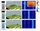
도 9는 본 발명의 실시예에 따라 LED를 배열하는 LED 배열 단계를 설명하기 위한 단면도이다. 도 10은 본 발명의 실시예에 따라 LED가 배열된 화소들을 나타내는 단면도이다. 도 11은 본 발명의 실시예에 따라 LED가 배열된 화소들을 나타내는 평면도이다. 도 12는 전극층들 사이에 발생하는 전기장을 시뮬레이션한 결과이다.9 is a cross-sectional view for explaining an LED arrangement step of arranging LEDs according to an embodiment of the present invention. 10 is a cross-sectional view illustrating pixels in which LEDs are arranged according to an embodiment of the present invention. 11 is a plan view illustrating pixels in which LEDs are arranged according to an exemplary embodiment of the present invention. 12 is a simulation result of an electric field generated between electrode layers.
도 9 내지 도 12를 참조하면, 절연층 형성 단계 이후 LED 배열 단계 동안 LED(ML)가 마이크로 LED 배열 영역(LAA)에 배열된다.Referring to FIGS. 9 to 12 , during the LED arranging step after the insulating layer forming step, the LEDs ML are arranged in the micro LED arranging area LAA.
LED 배열 단계 동안에는 기판(110) 상에 유체(FL)가 공급된다. 유체(FL)는 복수의 마이크로 LED들(ML)을 포함하고 있다.During the LED arranging step, the fluid FL is supplied on the
유체(FL)는 전기 신호 공급부(200)에 의해 전기 신호가 인가될 때 마이크로 LED(ML) 보다 낮은 유전상수(dielectric constant)를 갖는 액체일 수 있다.The fluid FL may be a liquid having a lower dielectric constant than that of the micro LED ML when an electrical signal is applied by the
실시예에 따라, 유체(FL)는 이소프로필알코올(isopropyl alcohol), 아세톤, 톨루엔 및 물 중에서 적어도 하나의 물질을 포함하는 액체일 수 있다.Depending on the embodiment, the fluid FL may be a liquid containing at least one of isopropyl alcohol, acetone, toluene, and water.
기판(110) 상에 복수의 마이크로 LED들(ML)이 포함된 유체(FL)가 공급되는 동안 전기 신호 공급부(200)가 제1 전극층(131)과 제2 전극층(133)에 전기 신호를 인가하여 제1 전극층(131)과 제2 전극층(133) 사이에 전기장(EF)을 생성시킨다.While the fluid FL including the plurality of micro LEDs ML is supplied on the
전기장(EF)이 생성되면 유체(FL)에 포함된 복수의 마이크로 LED들(ML) 중에서 어느 하나가 전기장(EF)의 인력에 의해 마이크로 LED 배열 영역(LAA)에 배열될 수 있다.When the electric field EF is generated, one of the plurality of micro LEDs ML included in the fluid FL may be arranged in the micro LED array area LAA by the attraction of the electric field EF.
이때, 제1 전극층(131)과 제2 전극층(133)은 전기장(EF)을 생성함과 동시에 다른 구성요소들, 예를 들어, 제1 전극층(131)과 제2 전극층(133) 아래의 기타 회로 등에 대한 전기장 차폐층 역할을 할 수 있다.At this time, the
전기 신호 공급부(200)는 제1 전극층(131)과 제2 전극층(133)으로 직류 신호, 교류 신호 또는 펄스 직류(pulsed DC) 신호를 공급할 수 있다.The electrical
전기 신호 공급부(200)는 마이크로 LED 배열 영역(LAA)에 배열되는 마이크로 LED(ML)의 방향이 일정하게 되도록 펄스 직류 신호를 제1 전극층(131)과 제2 전극층(133)으로 공급할 수 있다.The electric
여기서, 펄스 직류 신호는 값은 변하되 극성은 일정하게 유지되는 주기적인 전기 신호를 의미한다. 예를 들어, 전기 신호 공급부(200)는 교류 신호에 바이어스 직류 신호를 더하여 펄스 직류 신호를 생성할 수 있다.Here, the pulsed DC signal means a periodic electrical signal whose value is changed but whose polarity is maintained constant. For example, the electrical
도 10 내지 도 12은 마이크로 LED(ML)의 종류가 다양할 때의 LED 디스플레이(100)의 제조 방법을 설명하기 위한 도면이다.10 to 12 are views for explaining a manufacturing method of the
3가지 종류의 마이크로 LED들(ML1, ML2 및 ML3)가 있을 때에는 3번의 공정을 통해 3가지 종류의 마이크로 LED들(ML1, ML2 및 ML3)을 정확한 위치에 실장시킬 수 있다.When there are three types of micro LEDs (ML1, ML2, and ML3), the three types of micro LEDs (ML1, ML2, and ML3) can be mounted in precise positions through three processes.
먼저, 제1 마이크로 LED(ML1)을 실장시킬 때에는, 제1 마이크로 LED(ML1)가 포함된 유체(FL)를 공급하면서 전기 신호 공급부(200)가 제1 전극층(131)과 제2 전극층(133)에 전기 신호를 공급한다. 제1 전극층(131)과 제2 전극층(133) 사이에 인력이 발생하여 해당 부분에 제1 마이크로 LED(ML1)가 실장될 수 있다.First, when the first micro LED ML1 is mounted, the electrical
이때, 전기 신호 공급부(200)는 제3 전극층(135)와 제4 전극층(137)에는 전기 신호를 공급하지 않거나 제1 전극층(131) 또는 제2 전극층(133)과 인력이 발생하지 않도록 하는 전기 신호를 공급할 수 있다.At this time, the electrical
이후, 제2 마이크로 LED(ML2)을 실장시킬 때에는, 제2 마이크로 LED(ML2)가 포함된 유체(FL)를 공급하면서 전기 신호 공급부(200)가 제2 전극층(133)과 제3 전극층(135)에 전기 신호를 공급한다. 제2 전극층(133)과 제3 전극층(135) 사이에 인력이 발생하여 해당 부분에 제2 마이크로 LED(ML2)가 실장될 수 있다.Thereafter, when the second micro LED ML2 is mounted, the electrical
마지막으로, 제3 마이크로 LED(ML3)을 실장시킬 때에는, 제3 마이크로 LED(ML3)가 포함된 유체(FL)를 공급하면서 전기 신호 공급부(200)가 제3 전극층(135)과 제4 전극층(137)에 전기 신호를 공급한다. 제3 전극층(135)과 제4 전극층(137) 사이에 인력이 발생하여 해당 부분에 제3 마이크로 LED(ML3)가 실장될 수 있다.Finally, when the third micro LED (ML3) is mounted, the electrical
도 12에 도시된 각 조립(assembly) 과정마다 해당 마이크로 LED를 실장하기 위한 영역의 전극층들 사이에 전기장을 발생하여 LED 배열을 수행할 수 있음을 확인할 수 있다.It can be confirmed that the LED array can be performed by generating an electric field between the electrode layers in the region for mounting the corresponding micro LED in each assembly process shown in FIG. 12 .
도 13은 RGB 색상에 해당하는 나노 LED을 배열하는 방법을 보여주는 순서도이다.13 is a flowchart illustrating a method of arranging nano LEDs corresponding to RGB colors.
복수의 열 중에서, 각 열마다 전기 신호를 순차적으로 인가하여 서로 다른 발광특성을 가진 마이크로 LED, 예를 들어 R-G-B의 색상에 해당하는 나노 혹은 마이크로 LED를 디스플레이 백플레인 위에 디스플레이 화소로 배열할 수 있다. 이때, 순차적으로 전기장을 형성하기 위하여 개별적으로 전기신호를 가할 수 있는 회로장치를 사용하도록 한다.Among the plurality of columns, by sequentially applying an electric signal to each column, micro LEDs having different light emitting characteristics, for example, nano or micro LEDs corresponding to R-G-B colors, may be arranged as display pixels on the display backplane. At this time, in order to sequentially form an electric field, a circuit device capable of individually applying electric signals is used.
화소별로 전기장을 따로 적용하여 RGB 풀컬러를 구현하기 위해서는 순서에 상관없이 다음과 같은 방법으로 LED를 배열할 수 있다.In order to implement RGB full color by separately applying an electric field to each pixel, the LEDs can be arranged in the following way regardless of the order.
복수의 LED 중에서 적색 마이크로 LED가 포함된 유체를 공급하면서, 적색 화소에 포함되는 트랜지스터와 연결되는 제1 전극층과, 제2 전극층에 전기 신호를 인가하여, 적색 화소에 포함되는 마이크로 LED 배열 영역에 적색 마이크로 LED를 배열하고, 기판(백플레인)을 건조시킨다.While supplying a fluid containing red micro LEDs among a plurality of LEDs, by applying an electrical signal to the first electrode layer connected to the transistor included in the red pixel and the second electrode layer, a red light is applied to the micro LED array area included in the red pixel. Arrange the micro LEDs and dry the substrate (backplane).
또한 복수의 LED 중에서 녹색 마이크로 LED가 포함된 유체를 공급하면서, 녹색 화소에 포함되는 트랜지스터와 연결되는 제1 전극층과, 제2 전극층에 전기 신호를 인가하여, 녹색 화소에 포함되는 마이크로 LED 배열 영역에 녹색 마이크로 LED를 배열하고, 기판(백플레인)을 건조시킨다.In addition, while supplying a fluid containing a green micro LED among a plurality of LEDs, an electric signal is applied to the first electrode layer connected to the transistor included in the green pixel and the second electrode layer, thereby extending the micro LED array area included in the green pixel. Arrange the green micro LEDs, and dry the substrate (backplane).
또한 복수의 LED 중에서 청색 마이크로 LED가 포함된 유체를 공급하면서, 청색 화소에 포함되는 트랜지스터와 연결되는 제1 전극층과, 제2 전극층에 전기 신호를 인가하여, 청색 화소에 포함되는 마이크로 LED 배열 영역에 청색 마이크로 LED를 배열하고 기판(백플레인)을 건조시킨다.In addition, while supplying a fluid containing blue micro LEDs among a plurality of LEDs, an electrical signal is applied to the first electrode layer connected to the transistor included in the blue pixel and the second electrode layer, so that the micro LED array area included in the blue pixel Arrange the blue micro LEDs and dry the substrate (backplane).
이처럼, 유체 공급, 마이크로 LED 배열, 건조과정을 반복하여 R-G-B 나노 LED 어레이 형태를 디스플레이 위에 형성하고 전극 형성과 금속 전극 패터닝 공정 등을 사용하여 풀컬러 디스플레이 소자를 완성할 수 있다.In this way, the fluid supply, micro LED array, and drying processes are repeated to form an R-G-B nano LED array shape on the display, and a full-color display device can be completed by using electrode formation and metal electrode patterning processes.
도 14는 본 발명의 실시예에 따라 LED를 결합하는 LED 결합 단계와 소스 전극, 드레인 전극 및 전원 전극을 형성하는 전극 형성 단계를 설명하기 위한 단면도이다. 도 15는 본 발명의 실시예에 따라 LED 조립단계, 전극 형성 단계, 전극의 패터닝 및 소자 분리 단계를 나타내는 단면도이다.14 is a cross-sectional view for explaining an LED combining step of combining LEDs and an electrode forming step of forming a source electrode, a drain electrode, and a power supply electrode according to an embodiment of the present invention. 15 is a cross-sectional view showing steps of assembling LEDs, forming electrodes, patterning electrodes, and separating devices according to an embodiment of the present invention.
도 14 및 도 15를 참조하면, LED 배열 단계 이후 LED 결합 단계 동안 절연층(140)이 제거되고 마이크로 LED(ML)의 양단이 각각 제1 전극층(131)과 제2 전극층(133)에 결합된다.14 and 15, during the LED arranging step and the LED combining step, the insulating
도 14(a)에 도시된 바와 같이, 마이크로 LED(ML)가 배열된 절연층(140) 상에 포토레지스트(PR)를 도포한다. 도포된 포토레지스트(PR) 중에서 마이크로 LED(ML)의 양단에 대응하는 부분을 제거하여 포토레지스트 패턴을 형성한다. 형성된 포토레지스트 패턴을 식각 마스크를 사용하여 식각을 수행함으로써 절연층(140) 중에서 마이크로 LED(ML) 양단의 아래 부분을 제거한다.As shown in FIG. 14(a), a photoresist PR is applied on the insulating
이후, 도 14(b)에 도시된 바와 같이, 절연층(140)이 제거된 영역에 금속을 증착 또는 전기 도금하여 제1 고정 전극(151)과 제2 고정 전극(153)을 형성한다. 증착의 예로, 전착(electrodeposition, 전기 영동 증착)을 수행할 수 있다.Then, as shown in FIG. 14( b ), metal is deposited or electroplated on the region where the insulating
마이크로 LED(ML)의 일단은 제1 고정 전극(151)을 통해 제1 전극층(131)에 전기적으로 접속되며 물리적으로 고정될 수 있다. 동일하게, 마이크로 LED(ML)의 타단은 제2 고정 전극(153)을 통해 제2 전극층(133)에 전기적으로 접속되며 물리적으로 고정될 수 있다. 제1 고정 전극(151)과 제2 고정 전극(153)의 높이는 마이크로 LED 배열 영역(LAA)의 전극(131, 133)과의 거리에 맞춰 조절될 수 있으며, 도 13에 도시한 바와 같이 소정의 높이를 가지거나, 또는 도 14에 도시한 바와 같이 박막과 같은 층 형태일 수 있다.One end of the micro LED ML is electrically connected to the
도 14(b) 및 도 15에 도시된 바와 같이, 제1 전극층(131)과 제2 전극층(133) 상에 절연층이 잔류한 상태일 수 있다.As shown in FIGS. 14( b ) and 15 , an insulating layer may remain on the
이후, 도 14(c)에 도시된 바와 같이, 포토레지스트(PR)와 절연층(140)을 전체적으로 제거한다.Then, as shown in FIG. 14(c), the photoresist PR and the insulating
전술한 바와 같이, LED 결합 단계 이후, 상기 소스 및 드레인 전극용 금속층(130)을 패턴에 따라 식각하여 소스 전극(161) 및 드레인 전극(163), 전원 전극(165)을 형성할 수 있다.As described above, after the LED bonding step, the
도 14(d)에 도시된 바와 같이, 제1 전극층(131) 중에서 소정의 영역들, 즉, 활성층(125)의 상부 영역을 제거하고 제2 전극층(133)에서 베이스 회로(120)와 마이크로 LED(ML) 사이의 중간 영역을 제거하여 소스 전극(161), 드레인 전극(163) 및 전원 전극(165)을 생성한다.As shown in FIG. 14(d), predetermined regions of the
식각에 의해 전극이 분리됨에 따라, 소스 전극(161)의 좌측과 전원 전극(165)의 우측에 금속층(171, 173)이 남게 된다. 이러한 금속층(171, 173)은 마이크로 LED 디스플레이에서 2개의 트랜지스터와 1개의 캐패시터와 같은 복잡한 회로를 필요하는 경우, 인접한 전극으로 사용될 수 있다.As the electrodes are separated by etching, the metal layers 171 and 173 remain on the left side of the
이후, 도면에 도시되지는 않았으나, 필요에 따라, 완성된 회로, 즉, 소스 전극(161), 드레인 전극(163), 전원 전극(165), 고정 전극들(151, 153) 및 마이크로 LED(ML)를 보호할 수 있는 물질을 전체적으로 도포하여 LED 디스플레이(100)를 완성할 수 있다.Then, although not shown in the drawings, as necessary, the completed circuit, that is, the
이와 같이, 전기장을 이용해 마이크로 LED(ML)를 기판 상의 원하는 위치에 용이하게 실장시킬 수 있다. 더하여, 본 명세서에 기재되어 있는 실시예를 통해 보다 저렴하고 빠르면서 수율이 높은 LED 디스플레이를 제조할 수 있다.In this way, the micro LED (ML) can be easily mounted at a desired position on the substrate using an electric field. In addition, it is possible to manufacture LED displays that are cheaper, faster, and with higher yields through the embodiments described herein.
전술한 바와 같이, 본 발명에 따른 마이크로 LED 디스플레이는 기판 상에 배치되는 트랜지스터, 제1 전극층(131)과 제2 전극층(133), 제1 고정 전극(151)과 제2 고정 전극(153), 및 제1 고정 전극(151)과 제2 고정 전극(153)에 양단이 결합되는 LED를 포함한다.As described above, the micro LED display according to the present invention includes a transistor disposed on a substrate, a
구체적으로, 트랜지스터는 구동 트랜지스터(DT)를 가리키며, 전술한 바와 같이, 4가지 배치 구조를 갖는 트랜지스터 중 하나가 선택될 수 있다.Specifically, the transistor refers to the driving transistor DT, and as described above, one of the four arrangement structures may be selected.
제1 전극층(131)은 트랜지스터의 소스 전극 및 드레인 전극 중 어느 하나로부터 연장되는 것이다. 제2 전극층(133)은 상기 제1 전극층(131)과 수평적으로 이격되도록 상기 기판 상에 배치된다. 여기서 제2 전극층(133)은 전원 전압 라인(VDD) 또는 기저 전압 라인(Vss)에 연결될 수 있다.The
제1 고정 전극(151)은 제1 전극층(131)으로부터 상부 방향으로 연장되며, 제2 고정 전극(153)은 제2 전극층(133)으로부터 상부 방향으로 연장되어, 제1 고정 전극(151)과 제2 고정 전극(153)에 LED의 양단이 결합되는 구조이다.The first
제1 고정 전극(151)과 제2 고정 전극(153)은 서로 이격 배치되는 구조이다. 제1 전극층(131) 상부면 및 제2 전극층(133) 상부면으로부터 LED가 이격 배치되어 기판 표면으로부터 이격되므로 방열 효과를 부여할 수 있다.The first
갭 영역, 마이크로 LED 배열 영역 등에 대한 사항은 제조 방법에서 전술한 바와 동일하므로, 생략하기로 한다.Details on the gap area, the micro LED array area, and the like are the same as those described in the manufacturing method, and thus will be omitted.
이상과 같이 본 발명에 대해서 예시한 도면을 참조로 하여 설명하였으나, 본 명세서에 개시된 실시예와 도면에 의해 본 발명이 한정되는 것은 아니며, 본 발명의 기술사상의 범위 내에서 통상의 기술자에 의해 다양한 변형이 이루어질 수 있음은 자명하다. 아울러 앞서 본 발명의 실시예를 설명하면서 본 발명의 구성에 따른 작용 효과를 명시적으로 기재하여 설명하지 않았을 지라도, 해당 구성에 의해 예측 가능한 효과 또한 인정되어야 함은 당연하다.As described above, the present invention has been described with reference to the drawings illustrated, but the present invention is not limited by the embodiments and drawings disclosed herein, and various modifications are made by those skilled in the art within the scope of the technical idea of the present invention. It is obvious that variations can be made. In addition, although the operation and effect according to the configuration of the present invention have not been explicitly described and described while describing the embodiments of the present invention above, it is natural that the effects predictable by the corresponding configuration should also be recognized.
100; LED 디스플레이DT; 구동 트랜지스터
ST; 스위칭 트랜지스터Cst; 스토리지 커패시터
ML; 마이크로 LED121; 게이트 전극
123; 게이트 절연막125; 활성층
131; 제1 전극층133; 제2 전극층
140; 절연층151; 제1 고정 전극
153; 제2 고정 전극161; 소스 전극
163; 드레인 전극165; 전원 전극
171, 173; 금속층100; LED display DT; drive transistor
ST; switching transistor Cst ; storage capacitor
ML;
123;
131;
140; insulating
153; a second
163;
171, 173; metal layer
Claims (14)
Translated fromKorean상기 트랜지스터의 소스 전극 및 드레인 전극 중 어느 하나로부터 연장되는 제1 전극층과, 상기 제1 전극층과 수평적으로 이격되도록 상기 기판 상에 배치된 제2 전극층;
상기 제1 전극층으로부터 상부 방향으로 연장되는 제1 고정 전극과 상기 제2 전극층으로부터 상부 방향으로 연장되는 제2 고정 전극; 및
상기 제1 고정 전극 및 제2 고정 전극에 양단이 결합되는 LED;를 포함하고,
상기 제1 전극층 및 제2 전극층에 양단이 결합되는 LED는 제1 전극층 상부면 및 제2 전극층 상부면으로부터 이격 배치되는 마이크로 LED 디스플레이.
a transistor disposed on a substrate and including a gate electrode, a gate insulating film, an active layer, a source electrode, and a drain electrode;
a first electrode layer extending from any one of the source electrode and the drain electrode of the transistor, and a second electrode layer disposed on the substrate to be horizontally spaced apart from the first electrode layer;
a first fixed electrode extending upwardly from the first electrode layer and a second fixed electrode extending upwardly from the second electrode layer; and
An LED having both ends coupled to the first fixed electrode and the second fixed electrode,
The LED having both ends coupled to the first electrode layer and the second electrode layer is disposed spaced apart from the upper surface of the first electrode layer and the upper surface of the second electrode layer.
상기 트랜지스터는 바텀 게이트-탑 콘택트(bottom gate-top contact), 바텀 게이트-바텀 콘택트(bottom gate-bottom contact), 톱 게이트-탑 콘택트(top gate-top contact), 톱 게이트-바텀 콘택트(top gate-bottom contact) 중 어느 하나인 마이크로 LED 디스플레이.
According to claim 1,
The transistor includes a bottom gate-top contact, a bottom gate-bottom contact, a top gate-top contact, and a top gate-bottom contact. -bottom contact), which is a micro LED display.
상기 제1 전극층과 제2 전극층 사이에 갭 영역을 포함하고, 상기 갭 영역의 일부 영역에 중첩되는 마이크로 LED 배열 영역을 포함하는 마이크로 LED 디스플레이.
According to claim 1,
A micro LED display comprising a gap region between the first electrode layer and the second electrode layer, and a micro LED array region overlapping a partial region of the gap region.
상기 제1 전극층과 상기 제2 전극층은 서로를 향해 돌출되도록 배치되는 마이크로 LED 디스플레이.
According to claim 1,
The first electrode layer and the second electrode layer are disposed to protrude toward each other.
상기 LED는 1 ~ 100㎛의 길이를 갖는 나노와이어 형태인 마이크로 LED 디스플레이.
According to claim 1,
The LED is a micro LED display in the form of a nanowire having a length of 1 to 100 μm.
상기 제2 전극층은 전원 전압 라인(VDD) 또는 기저 전압 라인(Vss)에 연결되는 마이크로 LED 디스플레이.
According to claim 1,
The second electrode layer is connected to a power supply voltage line (VDD ) or a base voltage line (Vss).
(b) 상기 제1 전극층과 제2 전극층 사이의 갭 영역을 덮되, 상기 갭 영역 상의 일부 영역에 트렌치 구조의 마이크로 LED 배열 영역이 형성되도록 절연층을 형성하는 단계;
(c) 상기 기판 상에 LED가 포함된 유체를 공급하면서 상기 제1 전극층과 제2 전극층에 전기 신호를 인가하여 상기 LED를 상기 트렌치 구조의 마이크로 LED 배열 영역에 배열하는 단계;
(d) 상기 절연층 중에서 상기 LED의 양단의 아래 부분을 제거하는 단계;
(e) 상기 절연층이 제거된 영역에 상기 제1 전극층으로부터 상부 방향으로 연장되는 제1 고정 전극과 상기 제2 전극층으로부터 상부 방향으로 연장되는 제2 고정 전극을 형성하는 단계; 및
(f) 상기 LED의 양단을 상기 제1 고정 전극 및 제2 고정 전극에 결합하는 단계;를 포함하는 마이크로 LED 디스플레이 제조 방법.
(a) forming a transistor including a gate electrode, a gate insulating film, an active layer, and a metal layer for source and drain electrodes on a substrate, a first electrode layer extending from the metal layer for source and drain electrodes of the transistor, and the first electrode layer; forming second electrode layers on the substrate to be horizontally spaced apart from each other with a gap area;
(b) forming an insulating layer so as to cover a gap region between the first electrode layer and the second electrode layer, and to form a micro LED array region having a trench structure in a partial region on the gap region;
(c) arranging the LEDs in the micro LED array area of the trench structure by applying an electrical signal to the first electrode layer and the second electrode layer while supplying a fluid containing the LED on the substrate;
(d) removing lower portions of both ends of the LED from among the insulating layer;
(e) forming a first fixed electrode extending upwardly from the first electrode layer and a second fixed electrode extending upwardly from the second electrode layer in the region where the insulating layer is removed; and
(f) coupling both ends of the LED to the first fixed electrode and the second fixed electrode; Micro LED display manufacturing method comprising a.
상기 (f) 단계 이후에, 상기 소스 및 드레인 전극용 금속층을 식각하여 소스 전극 및 드레인 전극을 형성하는, 마이크로 LED 디스플레이 제조 방법.
According to claim 7,
After the step (f), the source and drain electrodes are formed by etching the metal layer for the source and drain electrodes, the micro LED display manufacturing method.
상기 절연층을 형성하는 단계는
(b1) 상기 제1 전극층, 상기 제2 전극층 및 상기 갭 영역 상에 상기 절연층을 형성하는 단계; 및
(b2) 상기 절연층 중에서 상기 갭 영역 상의 상기 일부 영역에 대응하는 부분을 부분 식각하여 상기 트렌치 구조의 마이크로 LED 배열 영역을 형성하는 단계;를 포함하는 마이크로 LED 디스플레이 제조 방법.
According to claim 7,
Forming the insulating layer
(b1) forming the insulating layer on the first electrode layer, the second electrode layer, and the gap region; and
(b2) forming a micro LED array region of the trench structure by partially etching a portion of the insulating layer corresponding to the partial region on the gap region;
상기 LED를 상기 트렌치 구조의 마이크로 LED 배열 영역에 배열하는 단계는
복수의 열 중에서, 각 열마다 전기 신호를 순차적으로 인가하되,
적색 마이크로 LED가 포함된 유체를 공급하면서, 적색 화소에 포함되는 트랜지스터와 연결되는 제1 전극층과, 제2 전극층에 전기 신호를 인가하여, 적색 화소에 포함되는 마이크로 LED 배열 영역에 적색 마이크로 LED를 배열하고 건조시키며,
녹색 마이크로 LED가 포함된 유체를 공급하면서, 녹색 화소에 포함되는 트랜지스터와 연결되는 제1 전극층과, 제2 전극층에 전기 신호를 인가하여, 녹색 화소에 포함되는 마이크로 LED 배열 영역에 녹색 마이크로 LED를 배열하고 건조시키며,
청색 마이크로 LED가 포함된 유체를 공급하면서, 청색 화소에 포함되는 트랜지스터와 연결되는 제1 전극층과, 제2 전극층에 전기 신호를 인가하여, 청색 화소에 포함되는 마이크로 LED 배열 영역에 청색 마이크로 LED를 배열하고 건조시키는, 마이크로 LED 디스플레이 제조 방법.
According to claim 7,
Arranging the LEDs in the micro LED array area of the trench structure
Among the plurality of columns, an electrical signal is sequentially applied to each column,
Red micro LEDs are arranged in the micro LED array area included in the red pixels by applying an electric signal to the first electrode layer connected to the transistor included in the red pixel and the second electrode layer while supplying the fluid containing the red micro LED. and dry,
While supplying a fluid containing green micro LEDs, an electric signal is applied to the first electrode layer connected to the transistor included in the green pixel and the second electrode layer, thereby arranging green micro LEDs in the micro LED array area included in the green pixel. and dry,
Blue micro LEDs are arranged in the micro LED array area included in the blue pixels by applying an electric signal to the first electrode layer connected to the transistor included in the blue pixel and the second electrode layer while supplying the fluid containing the blue micro LED. And drying, micro LED display manufacturing method.
상기 절연층 중에서 LED의 양단의 아래 부분을 제거하는 단계는
(d1) 상기 절연층과 상기 LED 상에 포토레지스트를 도포하는 단계;
(d2) 상기 포토레지스트 중에서 상기 LED의 상기 양단에 대응하는 부분을 제거하여 포토레지스트 패턴을 형성하는 단계; 및
(d3) 상기 포토레지스트 패턴을 식각 마스크로 사용하여 상기 절연층 중에서 상기 LED의 상기 양단의 아래 부분을 제거하는 단계;를 포함하는 마이크로 LED 디스플레이 제조 방법.
According to claim 7,
The step of removing the lower part of both ends of the LED from the insulating layer is
(d1) coating photoresist on the insulating layer and the LED;
(d2) forming a photoresist pattern by removing portions of the photoresist corresponding to both ends of the LED; and
(d3) using the photoresist pattern as an etch mask to remove portions below the both ends of the LED from among the insulating layer;
상기 제1 고정 전극과 제2 고정 전극은 상기 절연층이 제거된 영역에 금속을 증착 또는 전기 도금하여 형성되는 마이크로 LED 디스플레이 제조 방법.
According to claim 7,
The first fixed electrode and the second fixed electrode are formed by depositing or electroplating a metal in a region from which the insulating layer is removed.
상기 (f) 단계 이후에, 상기 절연층을 전부 제거하는 단계;를 더 포함하는 마이크로 LED 디스플레이 제조 방법.
According to claim 7,
After step (f), removing all of the insulating layer; Micro LED display manufacturing method further comprising.
Applications Claiming Priority (2)
| Application Number | Priority Date | Filing Date | Title |
|---|---|---|---|
| KR20190066331 | 2019-06-05 | ||
| KR1020190066331 | 2019-06-05 |
Publications (3)
| Publication Number | Publication Date |
|---|---|
| KR20200140209A KR20200140209A (en) | 2020-12-15 |
| KR102489507B1true KR102489507B1 (en) | 2023-01-17 |
| KR102489507B9 KR102489507B9 (en) | 2024-02-16 |
Family
ID=73780372
Family Applications (2)
| Application Number | Title | Priority Date | Filing Date |
|---|---|---|---|
| KR1020200018804AActiveKR102219187B1 (en) | 2019-06-05 | 2020-02-17 | Method for manufacturing a led display |
| KR1020200068589AActiveKR102489507B1 (en) | 2019-06-05 | 2020-06-05 | A micro led display and method for manufacturing the same |
Family Applications Before (1)
| Application Number | Title | Priority Date | Filing Date |
|---|---|---|---|
| KR1020200018804AActiveKR102219187B1 (en) | 2019-06-05 | 2020-02-17 | Method for manufacturing a led display |
Country Status (1)
| Country | Link |
|---|---|
| KR (2) | KR102219187B1 (en) |
Families Citing this family (6)
| Publication number | Priority date | Publication date | Assignee | Title |
|---|---|---|---|---|
| KR102442664B1 (en)* | 2021-01-27 | 2022-09-13 | 주식회사 어드밴스트뷰테크널러지 | Micro led device and method for manufacturing the same, and display device using the same |
| KR102739539B1 (en)* | 2022-05-13 | 2024-12-10 | 한양대학교 에리카산학협력단 | Method for aligning micro led using electrostatic repulsive force and method for manufacturing micro led display using the same |
| WO2022245147A1 (en)* | 2021-05-21 | 2022-11-24 | 한양대학교 에리카산학협력단 | Microled alignment method using electrostatic repulsion, and microled display manufacturing method using same |
| KR102801915B1 (en)* | 2021-07-27 | 2025-04-29 | 삼성디스플레이 주식회사 | Display device |
| WO2024058290A1 (en)* | 2022-09-16 | 2024-03-21 | 엘지전자 주식회사 | Display device |
| CN119008656B (en)* | 2024-10-24 | 2025-01-10 | 惠科股份有限公司 | Light-emitting structure, method for manufacturing light-emitting structure, and display device |
Family Cites Families (6)
| Publication number | Priority date | Publication date | Assignee | Title |
|---|---|---|---|---|
| JP4814394B2 (en) | 2010-03-05 | 2011-11-16 | シャープ株式会社 | Method for manufacturing light emitting device |
| KR101058880B1 (en) | 2010-05-07 | 2011-08-25 | 서울대학교산학협력단 | LED display device having active elements and method for manufacturing same |
| KR102574603B1 (en)* | 2016-07-15 | 2023-09-07 | 삼성디스플레이 주식회사 | Light emitting device and fabricating method thereof |
| KR102592276B1 (en)* | 2016-07-15 | 2023-10-24 | 삼성디스플레이 주식회사 | Light emitting device and fabricating method thereof |
| KR102707509B1 (en)* | 2016-12-19 | 2024-09-23 | 삼성디스플레이 주식회사 | Light emitting device and fabricating method thereof |
| KR20180077114A (en)* | 2018-06-22 | 2018-07-06 | 피에스아이 주식회사 | Electrical contacts improved nano-scale LED electrode assembly |
- 2020
- 2020-02-17KRKR1020200018804Apatent/KR102219187B1/enactiveActive
- 2020-06-05KRKR1020200068589Apatent/KR102489507B1/enactiveActive
Also Published As
| Publication number | Publication date |
|---|---|
| KR102219187B1 (en) | 2021-02-25 |
| KR20200140179A (en) | 2020-12-15 |
| KR102219187B9 (en) | 2024-02-16 |
| KR20200140209A (en) | 2020-12-15 |
| KR102489507B9 (en) | 2024-02-16 |
Similar Documents
| Publication | Publication Date | Title |
|---|---|---|
| KR102489507B1 (en) | A micro led display and method for manufacturing the same | |
| US11637222B2 (en) | Display device and method of manufacturing the same | |
| US20230066918A1 (en) | Display device and method of manufacturing the same | |
| US20210366978A1 (en) | Light emitting device and manufacturing method of the light emitting device | |
| CN113013193B (en) | Display device and method for manufacturing the same | |
| JP7154227B2 (en) | LED-OLED hybrid self-luminous display | |
| TWI489624B (en) | Oled device with embedded chip driving | |
| US9793252B2 (en) | Method of integrating inorganic light emitting diode with oxide thin film transistor for display applications | |
| CN104871231B (en) | Active matrix display panel with ground connection joint lines | |
| CN100355084C (en) | Double-plate type organic electroluminescent display device and manufacturing method | |
| US20210272938A1 (en) | Display device and method for manufacturing display device | |
| US11239215B2 (en) | Display device using semiconductor light emitting device and method for manufacturing the same | |
| US20160284267A1 (en) | Organic light-emitting diode display and manufacturing method thereof | |
| CN102576811A (en) | Amoled with cascaded OLED structures | |
| KR20210048290A (en) | Display device and method of fabricating the same | |
| KR20150040869A (en) | Display unit, method of manufacturing the same, and method of manufacturing electronic apparatus | |
| TW201618288A (en) | Display device and method of manufacturing same | |
| CN113994471B (en) | Micro light emitting diode display and method for manufacturing the same | |
| KR102859914B1 (en) | Pixel and display device including the same | |
| US11088198B2 (en) | Display device and manufacturing method of display device | |
| CN115732531A (en) | Display device and method of manufacturing the same | |
| US20250311508A1 (en) | Led display device comprising stacked micro-led elements and method for manufacturing same | |
| KR20220169061A (en) | Display device and method of fabricating the same | |
| CN110085625B (en) | Top-emission type display device and manufacturing method thereof | |
| US20250040325A1 (en) | Display device and method for manufacturing the same |
Legal Events
| Date | Code | Title | Description |
|---|---|---|---|
| PA0109 | Patent application | Patent event code:PA01091R01D Comment text:Patent Application Patent event date:20200605 | |
| PG1501 | Laying open of application | ||
| A201 | Request for examination | ||
| PA0201 | Request for examination | Patent event code:PA02012R01D Patent event date:20210115 Comment text:Request for Examination of Application Patent event code:PA02011R01I Patent event date:20200605 Comment text:Patent Application | |
| E902 | Notification of reason for refusal | ||
| PE0902 | Notice of grounds for rejection | Comment text:Notification of reason for refusal Patent event date:20220729 Patent event code:PE09021S01D | |
| E701 | Decision to grant or registration of patent right | ||
| PE0701 | Decision of registration | Patent event code:PE07011S01D Comment text:Decision to Grant Registration Patent event date:20230111 | |
| GRNT | Written decision to grant | ||
| PR0701 | Registration of establishment | Comment text:Registration of Establishment Patent event date:20230112 Patent event code:PR07011E01D | |
| PR1002 | Payment of registration fee | Payment date:20230112 End annual number:3 Start annual number:1 | |
| PG1601 | Publication of registration | ||
| G170 | Re-publication after modification of scope of protection [patent] | ||
| PG1701 | Publication of correction | Patent event code:PG17011E01I Patent event date:20240206 Comment text:Request for Publication of Correction Publication date:20240216 |