KR102486476B1 - Low power multilevel driver - Google Patents
Low power multilevel driverDownload PDFInfo
- Publication number
- KR102486476B1 KR102486476B1KR1020227012021AKR20227012021AKR102486476B1KR 102486476 B1KR102486476 B1KR 102486476B1KR 1020227012021 AKR1020227012021 AKR 1020227012021AKR 20227012021 AKR20227012021 AKR 20227012021AKR 102486476 B1KR102486476 B1KR 102486476B1
- Authority
- KR
- South Korea
- Prior art keywords
- input bits
- wire
- sub
- driver elements
- driver
- Prior art date
- Legal status (The legal status is an assumption and is not a legal conclusion. Google has not performed a legal analysis and makes no representation as to the accuracy of the status listed.)
- Active
Links
Images


Classifications
- G—PHYSICS
- G06—COMPUTING OR CALCULATING; COUNTING
- G06F—ELECTRIC DIGITAL DATA PROCESSING
- G06F13/00—Interconnection of, or transfer of information or other signals between, memories, input/output devices or central processing units
- G06F13/38—Information transfer, e.g. on bus
- G06F13/40—Bus structure
- G06F13/4063—Device-to-bus coupling
- G06F13/4068—Electrical coupling
- G06F13/4072—Drivers or receivers
- G—PHYSICS
- G06—COMPUTING OR CALCULATING; COUNTING
- G06F—ELECTRIC DIGITAL DATA PROCESSING
- G06F13/00—Interconnection of, or transfer of information or other signals between, memories, input/output devices or central processing units
- G06F13/38—Information transfer, e.g. on bus
- G06F13/42—Bus transfer protocol, e.g. handshake; Synchronisation
- G06F13/4204—Bus transfer protocol, e.g. handshake; Synchronisation on a parallel bus
- G06F13/4208—Bus transfer protocol, e.g. handshake; Synchronisation on a parallel bus being a system bus, e.g. VME bus, Futurebus, Multibus
- G—PHYSICS
- G06—COMPUTING OR CALCULATING; COUNTING
- G06F—ELECTRIC DIGITAL DATA PROCESSING
- G06F13/00—Interconnection of, or transfer of information or other signals between, memories, input/output devices or central processing units
- G06F13/38—Information transfer, e.g. on bus
- G06F13/42—Bus transfer protocol, e.g. handshake; Synchronisation
- G06F13/4265—Bus transfer protocol, e.g. handshake; Synchronisation on a point to point bus
- H—ELECTRICITY
- H04—ELECTRIC COMMUNICATION TECHNIQUE
- H04L—TRANSMISSION OF DIGITAL INFORMATION, e.g. TELEGRAPHIC COMMUNICATION
- H04L25/00—Baseband systems
- H04L25/02—Details ; arrangements for supplying electrical power along data transmission lines
- H04L25/0264—Arrangements for coupling to transmission lines
- H04L25/0272—Arrangements for coupling to multiple lines, e.g. for differential transmission
- H—ELECTRICITY
- H04—ELECTRIC COMMUNICATION TECHNIQUE
- H04L—TRANSMISSION OF DIGITAL INFORMATION, e.g. TELEGRAPHIC COMMUNICATION
- H04L25/00—Baseband systems
- H04L25/02—Details ; arrangements for supplying electrical power along data transmission lines
- H04L25/0264—Arrangements for coupling to transmission lines
- H04L25/028—Arrangements specific to the transmitter end
- Y—GENERAL TAGGING OF NEW TECHNOLOGICAL DEVELOPMENTS; GENERAL TAGGING OF CROSS-SECTIONAL TECHNOLOGIES SPANNING OVER SEVERAL SECTIONS OF THE IPC; TECHNICAL SUBJECTS COVERED BY FORMER USPC CROSS-REFERENCE ART COLLECTIONS [XRACs] AND DIGESTS
- Y02—TECHNOLOGIES OR APPLICATIONS FOR MITIGATION OR ADAPTATION AGAINST CLIMATE CHANGE
- Y02D—CLIMATE CHANGE MITIGATION TECHNOLOGIES IN INFORMATION AND COMMUNICATION TECHNOLOGIES [ICT], I.E. INFORMATION AND COMMUNICATION TECHNOLOGIES AIMING AT THE REDUCTION OF THEIR OWN ENERGY USE
- Y02D10/00—Energy efficient computing, e.g. low power processors, power management or thermal management
Landscapes
- Engineering & Computer Science (AREA)
- Theoretical Computer Science (AREA)
- General Engineering & Computer Science (AREA)
- Physics & Mathematics (AREA)
- General Physics & Mathematics (AREA)
- Computer Hardware Design (AREA)
- Power Engineering (AREA)
- Computer Networks & Wireless Communication (AREA)
- Signal Processing (AREA)
- Dc Digital Transmission (AREA)
Abstract
Translated fromKoreanDescription
Translated fromKorean본 출원은 2017년 9월 7일자로 미국에 출원되고, "저전력 멀티레벨 드라이버"로 명칭되며, Omid Talebi Amiri 및 Armin Tajalii를 지명하는 미국 출원 번호 제15/698,567호를 우선권으로 주장하며, 이 출원은 모든 목적들을 위해 그 전체가 참조로서 본원에 포함된다.This application claims priority to US Application Serial No. 15/698,567, filed in the United States on September 7, 2017, entitled "Low Power Multilevel Driver", to Omid Talebi Amiri and Armin Tajalii, which is incorporated herein by reference in its entirety for all purposes.
발명의 분야field of invention
본 실시예들은 일반적으로 통신 시스템 회로들, 더 상세하게 칩간 통신(chip-to-chip communication)을 위해 사용되는 고속 멀티 와이어 인터페이스(high-speed multi-wire interface)로의 멀티레벨 출력 신호들의 생성에 관한 것이다.The present embodiments relate generally to communication system circuits, and more particularly to the generation of multilevel output signals into high-speed multi-wire interfaces used for chip-to-chip communication. will be.
통신 시스템들에서, 하나의 물리적 위치로부터 다른 물리적 위치로 정보가 송신될 수 있다. 또한, 이 정보의 송신은 신뢰할 수 있고, 빠르며 최소량의 리소스들을 소비하는 것이 일반적으로 바람직하다. 가장 일반적인 정보 송신 매체들 중 하나는 직렬 통신 링크(serial communication link)인데, 이는 접지 또는 다른 공통 기준에 대한 단일 와이어 회로, 접지 또는 다른 공통 기준에 대한 복수의 그러한 회로들, 또는 서로 관련되어 사용되는 복수의 회로들을 기반으로 할 수 있다.In communication systems, information may be transmitted from one physical location to another. Also, it is generally desirable that the transmission of this information is reliable, fast and consumes the least amount of resources. One of the most common information transmission media is a serial communication link, which can be a single wire circuit to ground or other common reference, a plurality of such circuits to ground or other common reference, or It can be based on multiple circuits.
일반적인 경우에, 직렬 통신 링크는 다수의 시간 주기(time period)들에 걸쳐 사용된다. 각각의 그러한 시간 주기에서, 링크를 통하는 신호 또는 신호들은 전형적으로 비트들로 측정되는 일정량의 정보를 나타내며, 따라서 이를 전달한다. 따라서, 고 레벨에서, 직렬 통신 링크는 송신기를 수신기에 연결하고, 송신기는 각 시간 주기에 신호 또는 신호들을 송신하며, 수신기는 (링크를 통한 신호 열화(signal degradation), 노이즈, 및 다른 왜곡(distortion)들의 결과로서) 송신된 것에 가까운 신호 또는 신호들을 수신한다. 송신기에 의해 전달되는 정보는 송신기에 의해 "소비"되며, 대표적인 신호들이 생성된다. 수신기는 자신이 수신한 신호들로부터의 전달된 정보를 결정하려고 시도한다. 전체적인 에러들이 없는 경우에, 수신기는 송신기에 의해 소비된 비트들을 정확하게 출력할 수 있다.In the general case, a serial communication link is used over multiple time periods. In each such period of time, the signal or signals across the link represent, and thus convey, some amount of information, typically measured in bits. Thus, at a high level, a serial communication link connects the transmitter to the receiver, the transmitter transmits a signal or signals each time period, and the receiver transmits (signal degradation, noise, and other distortion over the link) ) as a result of) receiving a signal or signals close to the one transmitted. The information conveyed by the transmitter is "consumed" by the transmitter, and representative signals are generated. A receiver attempts to determine the conveyed information from the signals it receives. In the absence of gross errors, the receiver can accurately output the bits consumed by the transmitter.
직렬 통신 링크의 일례는 차분 시그널링(differential signaling: DS) 링크이다. 차분 시그널링은 하나의 와이어 상에 신호를 전송하고 쌍을 이룬(paired) 와이어 상에 이 신호의 역(opposite)을 전송함으로써 동작하며; 신호 정보는 접지 또는 다른 고정된 기준에 대한 절대값들보다는 와이어들 간의 차로 표시된다. 차분 시그널링은 크로스토크(crosstalk) 및 다른 공통 모드 노이즈를 캔슬링(cancelling)함으로써, 싱글 엔디드 시그널링(single ended signaling: SES)에 비해 수신기에서의 원래 신호의 복구성(recoverability)을 향상시킨다. DS에 비해 핀 효율을 증가시키면서 DS의 바람직한 특성들을 유지하는 다수의 시그널링 방법들이 있다. 이러한 시도들의 대부분은, 2개보다 많은 와이어들 상에서 동시에, 각 와이어 상에서 이진(binary) 신호들을 사용하지만 그룹들의 비트들로 정보를 맵핑하여 동작한다.An example of a serial communication link is a differential signaling (DS) link. Differential signaling works by sending a signal on one wire and the opposite of this signal on a paired wire; Signal information is represented by differences between wires rather than absolute values relative to ground or other fixed reference. Differential signaling improves the recoverability of the original signal at the receiver compared to single ended signaling (SES) by canceling crosstalk and other common mode noise. There are a number of signaling methods that increase pin efficiency compared to DS while maintaining the desirable characteristics of DS. Most of these attempts work by using binary signals on each wire, simultaneously on more than two wires, but mapping the information into groups of bits.
벡터 시그널링은 시그널링의 방법이다. 벡터 시그널링의 경우에, 복수의 와이어들 상의 복수의 신호들이 집합적으로 고려되지만 복수의 신호들 각각은 독립적일 수 있다. 집합 신호들 각각은 컴포넌트로 지칭되고, 복수의 와이어들의 개수는 벡터의 "차원(dimension)"으로 지칭된다. 일부 실시예들에서, DS 쌍들의 경우와 같이, 하나의 와이어 상의 신호는 다른 와이어 상의 신호에 전적으로 종속적이며, 그래서 일부 경우들에서 벡터의 차원은 복수의 와이어들의 와이어들의 개수 대신 복수의 와이어들 상의 신호들의 자유도(degrees of freedom)의 개수를 지칭할 수 있다.Vector signaling is a method of signaling. In the case of vector signaling, multiple signals on multiple wires are collectively considered, but each of the multiple signals may be independent. Each of the aggregated signals is referred to as a component, and the number of multiple wires is referred to as the "dimension" of the vector. In some embodiments, as in the case of DS pairs, the signal on one wire is entirely dependent on the signal on the other wire, so in some cases the dimension of a vector is the number of wires in the plurality of wires instead of the number of wires in the plurality of wires. It may refer to the number of degrees of freedom of signals.
이진 벡터 시그널링(binary vector signaling)의 경우에, 각 컴포넌트는 2개의 가능한 값들 중 하나인 좌표값(또는 줄여서 "좌표")을 취한다. 예로서, 8개의 SES 와이어들이 집합적으로 고려될 수 있는데, 각 컴포넌트/와이어는 각 신호 주기에서 2개의 값들 중 하나를 취한다. 이 이진 벡터 시그널링의 "코드워드(code word)"는 이 집합적 세트의 컴포넌트들/와이어들의 가능한 상태들 중 하나이다. "벡터 시그널링 코드" 또는 "벡터 시그널링 벡터 세트"는 주어진 벡터 시그널링 인코딩 스키마에 대한 유효하고 가능한 코드워드들의 컬렉션이다. "이진 벡터 시그널링 코드"는 맵핑 및/또는 정보 비트들을 이진 벡터들에 맵핑하기 위한 한 세트의 규칙들을 지칭한다. 각 컴포넌트가 2개의 가능한 좌표들 중 하나가 될 수 있는 자유도를 갖는 8개의 SES 와이어들의 예에서, 코드워드들의 컬렉션 내의 코드워드들의 수는 2^8개, 또는 256개이다. SES 또는 DS 링크들과 같이, 이진 벡터 시그널링 코드와 함께 사용되는 출력 드라이버들은 각 벡터 요소에 대해 2개의 가능한 좌표값들에 대응하는 2개의 별개의 전압 또는 전류 레벨들만 방출하면 된다.In the case of binary vector signaling, each component takes on a coordinate value (or "coordinate" for short) that is one of two possible values. As an example, eight SES wires can be considered collectively, with each component/wire taking one of two values in each signal period. The "code word" of this binary vector signaling is one of the possible states of the components/wires of this collective set. A “vector signaling code” or “vector signaling vector set” is a collection of valid and possible codewords for a given vector signaling encoding scheme. "Binary vector signaling code" refers to mapping and/or a set of rules for mapping information bits to binary vectors. In the example of 8 SES wires with each component having degrees of freedom to be in one of 2 possible coordinates, the number of codewords in the collection of codewords is 2^8, or 256. Output drivers used with binary vector signaling code, such as SES or DS links, need only emit two distinct voltage or current levels corresponding to the two possible coordinate values for each vector element.
비이진(non-binary) 벡터 시그널링의 경우에, 각 컴포넌트는 한 세트의 2개보다 많은 가능한 값들로부터 선택되는 좌표값을 갖는다. "비이진 벡터 시그널링 코드"는 맵핑 및/또는 정보 비트들을 비이진 벡터들에 맵핑하기 위한 한 세트의 규칙들을 지칭한다. 비이진 벡터 시그널링 코드에 대한 대응하는 출력 드라이버는 각 벡터 출력에 대해 선택된 좌표 값들에 대응하는 다수의 전압 또는 전류 레벨들을 방출하도록 구성 가능하다.In the case of non-binary vector signaling, each component has a coordinate value selected from a set of more than two possible values. "Non-binary vector signaling code" refers to a mapping and/or set of rules for mapping information bits to non-binary vectors. A corresponding output driver for the non-binary vector signaling code is configurable to emit multiple voltage or current levels corresponding to selected coordinate values for each vector output.
벡터 시그널링 방법들의 예들은 [Cronie I] 및 [Shokrollahi I]에서 설명된다. 직교 차분 벡터 시그널링(Orthogonal Differential Vector Signaling: ODVS) 코드들로 알려진, 이들이 설명하는 한 클래스의 벡터 시그널링 코드들은 "직교" 행렬에 의해 정의되는데, 직교 행렬에서 모든 행들은 서로 직교하며, 행렬과 행렬의 전치(transpose)의 곱(product)은 대각선 상에만 0이 아닌 값들을 갖는 행렬이다. ODVS 코드에 의해 통신되는 인코딩된 신호는, 각각 통신되는 데이터의 독립적인 요소로 변조되는 다수의 서브채널 신호들의 합산이다.Examples of vector signaling methods are described in [Cronie I] and [Shokrollahi I]. One class of vector signaling codes they describe, known as Orthogonal Differential Vector Signaling (ODVS) codes, is defined by an “orthogonal” matrix, in which all rows are orthogonal to each other, matrix-to-matrix The product of the transpose is a matrix with non-zero values only on the diagonal. An encoded signal communicated by an ODVS code is the sum of multiple subchannel signals, each modulated into an independent element of the communicated data.
송신기와 수신기는 직렬 통신 링크를 사용하여 통신할 수 있는데, 직렬 통신 링크는 평형 벡터(balanced vector) 시그널링 코드에 기초한 시그널링을 사용한다. 벡터 시그널링 코드는 각 송신 단위 간격으로 통신 링크의 다수의 와이어들을 사용하여 심벌들의 벡터를 송신한다. 벡터의 컴포넌트들의 개수는 2개, 3개, 4개, 또는 4개 이상일 수 있다. 컴포넌트에 대한 좌표 값들의 개수는 2개, 3개, 4개, 또는 4개 이상일 수 있다. 예를 들어, 링크는 4개의 가능한 좌표 값들 - 높은 값, 낮은 값, 및 높은 값과 낮은 값의 반수(inverse) - 을 갖는 4개의 컴포넌트들을 사용할 수 있으며, 높은 값을 갖는 신호는 낮은 값의 반수를 갖는 3개의 신호들을 상쇄시키고(cancel out), 높은 값의 반수를 갖는 신호는 낮은 값을 갖는 3개의 신호들을 상쇄시키며, 이러한 방식으로, 8개의 가능한 3 비트 조합들을, 3개의 낮은 값들의 반수들과 하나의 높은 값의 4개의 순열(permutation)들 및 3개의 낮은 값들과 하나의 높은 값의 반수의 4개의 순열들로 표현되는 8개의 벡터 코드워드들에 맵핑함으로서, 링크는 이들 4개의 컴포넌트들을 사용하여 신호 주기에 3 비트를 전달할 수 있다. 보다 구체적인 실시예에서, 높은 값과 낮은 값은 전압 값들이며 기준값에 대한 것이고, 높은 값과 그 반수는 크기는 같지만 반대의 부호(sign)들을 가지며, 낮은 값과 그 반수도 크기는 같지만 반대의 부호들을 가지며, 높은 값은 낮은 값의 3배의 크기를 갖는다. 다른 예로서, 상이한 링크는 3개의 가능한 좌표 값들 - 양(positive)의 값, 보다 작은 양의 값, 및 가장 작은 양의 값 또는 0 - 으로부터 선택된 3개의 컴포넌트들을 사용할 수 있으며, 모든 벡터 컴포넌트 값들의 합은 상수이다. 그러한 코드는 또한 평형을 이루지만, 싱글 엔드(single-ended) 전원 공급 장치들에 의존하는 실시예들에서 일반적인 관행처럼, 추가 오프셋 또는 DC 컴포넌트가 모든 가능한 좌표 값들에 중첩된다.The transmitter and receiver may communicate using a serial communication link, which uses signaling based on balanced vector signaling codes. A vector signaling code transmits a vector of symbols using multiple wires of a communication link at each transmission unit interval. The number of components in the vector may be two, three, four, or more than four. The number of coordinate values for a component may be 2, 3, 4, or more than 4. For example, a link can use four components with four possible coordinate values - a high value, a low value, and the inverse of the high value and the low value, and the signal with the high value is the half of the low value. cancels out the three signals with the high value half, and the signal with the high value cancels out the three signals with the low value, in this way, the eight possible 3-bit combinations, the three low half values By mapping to 8 vector codewords represented by 4 permutations of s and 4 permutations of one high value and 3 low values and 1 half of a high value, the link is made up of these 4 components can be used to convey 3 bits in a signal period. In a more specific embodiment, the high and low values are voltage values and are relative to the reference value, the high value and its half have equal magnitudes but opposite signs, and the low value and its half also magnitudes but opposite signs. , with higher values having three times the magnitude of lower values. As another example, a different link can use three components selected from three possible coordinate values—a positive value, a lesser positive value, and the smallest positive value or 0—of all vector component values. The sum is a constant. Such a code is also balanced, but as is common practice in embodiments relying on single-ended power supplies, an additional offset or DC component is superimposed on all possible coordinate values.
복수의 드라이버들에서 한 세트의 입력 비트들을 수신하고 신호들의 앙상블을 응답적으로 생성하기 위한 방법들 및 시스템들이 설명되며, 신호들의 앙상블의 각각의 신호는, 멀티 와이어 버스의 개개의 와이어에 연결된 개개의 드라이버에서 한 서브세트의 입력 비트들을 수신하고 - 수신된 한 서브세트의 비트들은 개개의 와이어와 연관된 서브채널들에 대응함 - , 복수의 가중 아날로그 신호 컴포넌트들을 생성하고 - 각각의 가중 아날로그 신호 컴포넌트는 (i) 개개의 와이어와 연관된 한 세트의 와이어 특유의(wire-specific) 서브채널 가중치들로부터 선택된 대응하는 가중치 및 부호를 갖고 (ii) 수신된 한 서브세트의 비트들 중 대응하는 비트에 의해 변조됨 - , 및 멀티 와이어 버스의 개개의 와이어를 통한 송신을 위해 개개의 와이어에 연결된 공통 노드(common node)에서 복수의 가중 아날로그 신호 컴포넌트들의 합산을 형성함으로써 개개의 신호를 생성함으로써 생성된다.Methods and systems are described for receiving a set of input bits in a plurality of drivers and responsively generating an ensemble of signals, each signal of the ensemble of signals being a separate wire connected to a respective wire of a multi-wire bus. Receive a subset of input bits at the driver of, wherein the received subset of bits corresponds to subchannels associated with an individual wire, generate a plurality of weighted analog signal components, each weighted analog signal component (i) with a corresponding weight and sign selected from a set of wire-specific subchannel weights associated with an individual wire, and (ii) modulated by a corresponding bit from a received subset of bits. , and generating an individual signal by forming a sum of a plurality of weighted analog signal components at a common node connected to the individual wires for transmission over the individual wires of the multi-wire bus.
적어도 하나의 실시예에 따르면, 프로세스들 및 장치들은, 멀티 칩 시스템에서 집적 회로 칩들을 상호 연결하는 것과 같이, 저전력 이용에서 높은 총 대역폭을 제공하는 고속의 저레이턴시(low latency) 인터페이스를 제공하기 위해 물리 채널들을 통해 데이터를 송신하는 것을 제공한다. 일부 실시예들에서, 상이한 전압, 전류 등의 레벨들이 시그널링을 위해 사용되며, 각각의 와이어 신호가 4개의 값들 중 하나를 갖는 4중(quaternary) 시그널링 시스템과 같이, 2개보다 많은 레벨들이 사용될 수 있다.According to at least one embodiment, processes and devices are used to provide a high speed, low latency interface that provides high aggregate bandwidth at low power usage, such as interconnecting integrated circuit chips in a multi-chip system. It provides for transmitting data over physical channels. In some embodiments, different voltage, current, etc. levels are used for signaling, and more than two levels can be used, such as in a quaternary signaling system where each wire signal has one of four values. there is.
본 발명의 개요는 아래의 상세한 설명에서 추가로 설명되는 개념의 집합을 단순화된 형태로 소개하기 위해 제공된다. 본 발명의 개요는 청구된 주제의 주요 또는 본질적인 특징을 식별하기 위한 것도 아니고, 청구된 주제의 범위를 결정하는 데 도움을 주기 위해 사용되기 위한 것도 아니다. 본 실시예들의 다른 양태들은 상세한 설명 및 포함된 도면들을 검토함에 따라 본 기술분야의 통상의 기술자에게 명백할 것이다.This summary of the invention is provided to introduce a set of concepts in a simplified form that are further described below in the Detailed Description. This summary is not intended to identify key or essential features of the claimed subject matter, nor is it intended to be used as an aid in determining the scope of the claimed subject matter. Other aspects of the present embodiments will become apparent to those skilled in the art upon review of the detailed description and included drawings.
도 1은 일부 실시예들에 따른 통신 시스템의 블록도이다.
도 2는 멀티 와이어 통신 채널의 단일 와이어에 대한 멀티레벨 라인 드라이버의 실시예의 개략도이다.
도 3 내지 도 7은 멀티 와이어 통신 채널의 개개의 와이어를 구동하도록 각각 구성된, 멀티레벨 라인 드라이버 실시예들의 추가 버전들을 도시한다.
도 8은 도 2에 사용된 것과 같은, 멀티레벨 라인 드라이버 요소의 다른 실시예의 개략도이다.
도 9는 출력 데이터의 4상(four phases)을 단일의 고속 출력 스트림으로 조합하기 위해 고속 멀티플렉서들을 통합한, 멀티레벨 라인 드라이버의 추가 실시예의 개략도이다.
도 10은 일부 실시예들에 따른 방법의 흐름도이다.1 is a block diagram of a communication system in accordance with some embodiments.
2 is a schematic diagram of an embodiment of a multi-level line driver for a single wire of a multi-wire communication channel.
3-7 show additional versions of multilevel line driver embodiments, each configured to drive an individual wire of a multi-wire communication channel.
8 is a schematic diagram of another embodiment of a multilevel line driver element, such as that used in FIG. 2;
9 is a schematic diagram of a further embodiment of a multilevel line driver incorporating high-speed multiplexers to combine the four phases of output data into a single high-speed output stream.
10 is a flow diagram of a method according to some embodiments.
[Cronie I] 및 [Shokrollahi I]에서 설명되는 바와 같이, 벡터 시그널링 코드들은 전형적으로 다수의 본질적으로 평행한 와이어들을 포함하는 통신 매체를 통한 데이터의 효율적인 통신을 가능하게 한다. 직교 차분 벡터 시그널링(ODVS) 코드들의 경우, 최대 N-1 비트의 이진 데이터가 N 와이어 채널을 통해 캐리될 수 있다. 그러한 시스템을 N-1 비트를 N 요소 코드워드로 인코딩하는 것으로 설명하는 것이 관행이며, 코드워드는 각 단위 간격(unit interval)에서 송신의 집단적 상태(aggregate state)를 나타내고, 각 코드워드 요소는 각 와이어의 특정 출력 상태에 대응하는 M개의 가능한 값들의 알파벳으로부터 취출된다(drawn).As described in [Cronie I] and [Shokrollahi I], vector signaling codes enable efficient communication of data over a communication medium that typically includes multiple essentially parallel wires. For Orthogonal Difference Vector Signaling (ODVS) codes, up to N-1 bits of binary data can be carried over an N wire channel. It is customary to describe such systems as encoding N-1 bits into N-element codewords, where each codeword represents the aggregate state of transmission in each unit interval, and each codeword element is It is drawn from an alphabet of M possible values corresponding to a particular output state of the wire.
[Shokrollahi I]의 Glasswing 코드를 예로 사용하면, 4개의 별개의 값들의 알파벳을 이용하여 5개의 이진 비트가 6개의 심벌 코드워드로 인코딩될 수 있다. 따라서, 6개의 와이어들을 통한 Glasswing 코드의 병렬 송신은, 각각이 4개의 전압 또는 전류 레벨들 중 하나를 6개의 와이어 통신 채널 중 하나의 와이어로 구동하도록 구성되는 6개의 단일 와이어 출력 드라이버들을 사용한다. Glasswing 코드의 고성능 변형은 10개의 값들의 알파벳을 이용하는데, 그러한 실시예들은 10개의 별개의 값들을 생성하는 출력 드라이버들을 이용한다.Using the Glasswing code of [Shokrollahi I] as an example, 5 binary bits can be encoded into 6 symbol codewords using an alphabet of 4 distinct values. Thus, parallel transmission of Glasswing code over six wires uses six single wire output drivers, each configured to drive one of the four voltage or current levels into one wire of the six wire communication channel. A high-performance variant of the Glasswing code uses an alphabet of 10 values; such embodiments use output drivers that produce 10 distinct values.
전형적으로 벡터 시그널링 코드들과 연계하여 사용되는 고 데이터 레이트(high data rate)들(일례로, [Shokrollahi I]는 초당 25 기가 코드워드(Giga-codewords), 즉 40 피코초의 단위 간격으로 동작하는 Glasswing 코드의 일 실시예를 설명함)에서, 출력 드라이버들은 구동 전류를 제공할 뿐만 아니라 송신 라인 임피던스를 매칭하는 것을 용이하게 하기 위해 낮고, 안정적인 출력 임피던스를 제공하기 위해 상당히 큰 출력 트랜지스터들을 포함한다. 병행되는 문제로서, 많은 고속 집적 회로 프로세스들은 비교적 높은 옴/스퀘어(ohms-per-square) 저항 재료만을 제공하며, 드라이버 라인 종단에 필요한 수십 옴의 저항기들의 제조가 문제된다.High data rates typically used in conjunction with vector signaling codes (e.g. [Shokrollahi I] is Glasswing operating at 25 Giga-codewords per second, i.e. unit intervals of 40 picoseconds). In one embodiment of the code), the output drivers include fairly large output transistors to provide drive current as well as low, stable output impedance to facilitate matching the transmission line impedance. As a parallel problem, many high-speed integrated circuit processes only provide relatively high ohms-per-square resistance materials, and fabrication of the tens of ohm resistors needed to terminate a driver line is problematic.
도 1은 일부 실시예들에 따른 예시적인 시스템을 도시한다. 도시된 바와 같이, 도 1은 소스 데이터 S0 내지 S4(100) 및 Clk(105)를 수신하는 송신기(110), 및 라인 드라이버(118)를 통한 다수의 와이어들(125)을 갖는 멀티 와이어 버스를 포함하는 채널(120)을 통하는 송신을 위한 정보를 인코딩하는 인코더(112)를 포함한다. 도 1은 검출기(132)를 포함하는 수신기(130)를 더 포함하고, 일부 실시예들에서, 필요된다면, 수신 데이터 R0 내지 R4(140) 및 수신 클록 Rclk(145)을 생성하기 위한 디코더(138)를 포함한다.1 shows an example system in accordance with some embodiments. As shown, FIG. 1 shows a
병렬 출력 드라이버 요소들Parallel Output Driver Elements
[Ulrich I]에서 설명되는 바와 같이, 보다 효율적인 실시예는 보다 작은 구동 트랜지스터들 및 보다 높은 값의 출력 저항기들을 각각 사용하는 다수의 병렬 라인 드라이버 요소들을 사용하는데, 다수의 요소들의 병렬 집단이 구동 전류 및 매칭된 라인 임피던스를 제공한다. 그러한 아키텍처에서, 각 송신 라인 와이어로의 최종 출력은 그 와이어에 대한 드라이버 요소들 모두에 대한 아날로그 합산 노드(analog summation node)이며, 중간 출력 전압들은 고출력 또는 저출력을 생성하는 상이한 개수들의 드라이버 요소들의 합산에 의해 생성된다. [Ulrich I]는 또한, 신호간 간섭(inter-signal interfereence: ISI), 파형 성형(waveform shaping), 및 다른 신호 보상을 위한 프리-커서(pre-cursor) 및/또는 포스트-커서(post-cursor) 보상을 제공하는, 유한 임펄스 응답(Finite Impulse Response: FIR) 수정(correction)들로 코드워드 출력을 증강시키기 위한 추가 세트들의 드라이버 요소들의 통합을 설명한다.As described in [Ulrich I], a more efficient embodiment uses multiple parallel line driver elements, each using smaller drive transistors and higher value output resistors, where a parallel group of multiple elements can generate a drive current and matched line impedance. In such an architecture, the final output to each transmission line wire is an analog summation node for all of the driver elements for that wire, and the intermediate output voltages are the summation of different numbers of driver elements that produce either high or low output. is created by [Ulrich I] also provides pre-cursor and/or post-cursor for inter-signal interference (ISI), waveform shaping, and other signal compensation. ) describes the integration of additional sets of driver elements to augment the codeword output with Finite Impulse Response (FIR) corrections that provide compensation.
[Amiri I]는 저 전력 소비로 멀티레벨 벡터 시그널링 코드 출력들을 생성하기 위해 다수의 병렬 드라이버 요소들을 이용하는 단순화된 실시예를 설명한다.[Amiri I] describes a simplified embodiment that uses multiple parallel driver elements to generate multilevel vector signaling code outputs with low power consumption.
이들 전술한 벡터 시그널링 코드의 실시예들에서, 송신되는 데이터는 인코더에 의해 처리되며, 출력 와이어 당 하나의 심벌을 포함하는 코드워드를 초래하며, 이 코드워드는 이어서 통신 매체의 다수의 와이어들에 본질적으로 병렬로 동기적으로 출력된다. 단일 이진 신호를 하나의 와이어에빌딩 블록(building block)으로서 방출할 수 있는 개별 출력 드라이버 요소를 사용하면, 이들 실시예들의 아키텍처는, 코드워드 폭(즉, 와이어들의 개수)을 지원하기 위해 수직으로 복제되고, 심벌 알파벳(즉, 코드워드 내의 각 심벌에 의해 표시되는 신호 레벨들의 개수)을 지원하기 위해 깊이로 복제되는 것으로서 설명될 수 있다.In these aforementioned embodiments of the vector signaling code, data to be transmitted is processed by an encoder, resulting in a codeword containing one symbol per output wire, which codeword is then spread over multiple wires of the communication medium. In essence, they are output synchronously in parallel. Using a separate output driver element capable of emitting a single binary signal on a single wire as a building block, the architecture of these embodiments can be used vertically to support codeword widths (i.e., number of wires). It is replicated and can be described as being replicated in depth to support a symbol alphabet (i.e., the number of signal levels represented by each symbol in a codeword).
출력 드라이버 내에서의 와이어링 복잡도(wiring complexity)Wiring complexity within the output driver
각 심벌이 취출되는 알파벳이 많은 요소들(Glasswing 코드의 2개의 전술한 변형들에 대해 4개 또는 10개)을 가질 수 있으므로, 인코더 출력으로부터 각 와이어의 출력 드라이버로 각 심벌 값의 인코딩된 표현을 전달하기 위해 다수의 신호 와이어들이 필요된다. 또한, 실용적인 고속 실시예들에서, 보다 높은 처리량(processing throughput)을 달성하기 위해 다수의 처리 위상(processing phase)들이 사용될 수 있으며, 최종 고속 멀티플렉서는 출력 전에, 조합된 데이터 스트림을 생성한다. [Ulrich I]는 각 심벌이 4 비트 값으로 인코딩되는 6 심벌 코드워드의 4상 처리의 예를 제공하며, 따라서 이 실시예에서 적어도 4 × 6 × 4의 신호가 인코더 출력으로부터 출력 드라이버로 라우팅되는데, 이는 상당한 신호 라우팅 복잡도를 시사한다.Since the alphabet from which each symbol is retrieved can have many elements (either 4 or 10 for the two aforementioned variants of the Glasswing code), the encoded representation of each symbol's value is sent from the encoder output to the output driver on each wire. Multiple signal wires are required to transmit. Also, in practical high-speed embodiments, multiple processing phases may be used to achieve higher processing throughput, with a final high-speed multiplexer generating the combined data stream prior to output. [Ulrich I] gives an example of 4-phase processing of a 6-symbol codeword where each symbol is encoded as a 4-bit value, so in this embodiment at least 4 x 6 x 4 signals are routed from the encoder output to the output driver. , which implies significant signal routing complexity.
서브채널 출력 드라이버Subchannel output driver
도 2에 도시된 실시예는 멀티레벨 출력 신호들을 집합적으로 생성하는 - 하지만 상이한 조직(organization)에서 이루어짐 - 복수의 드라이버 요소들([Ulrich I]에 의해 사용되는 용어에서는 "슬라이스(slice)")을 또한 이용한다. 도시된 바와 같이, 신호들의 앙상블(ensemble)의 각 신호는 대응하는 데이터에 의한 개별 서브채널들의 변조들에 기초하며, 각각의 변조된 서브채널은 아날로그 신호 컴포넌트를 생성한다. 신호들의 앙상블의 신호는 따라서, 생성할 아날로그 신호 컴포넌트들의 합산에 의해 형성된다. 일부 실시예들에서, 신호는 심벌에 대응하고, 신호들(심벌들)의 앙상블은 인코딩된 출력 코드워드에 대응한다. 제한을 의미함이 없이 설명을 목적으로, 이 예에서는, 하나의 데이터 비트에 의해 각각 변조된 5개의 직교 서브채널들에 더해, 공통 모드 신호 컴포넌트를 포함하는 [Shokrollahi I]의 "등안(equal eyes)" 5b6w_10_5 Glasswing 코드를 사용할 것이다.The embodiment shown in FIG. 2 consists of a plurality of driver elements ("slice" in a term used by [Ulrich I]) that collectively - but in different organizations - generate multilevel output signals. ) is also used. As shown, each signal of the ensemble of signals is based on modulations of individual subchannels with corresponding data, each modulated subchannel producing an analog signal component. A signal of the ensemble of signals is thus formed by the summation of the analog signal components to be generated. In some embodiments, a signal corresponds to a symbol, and an ensemble of signals (symbols) corresponds to an encoded output codeword. For purposes of explanation and not meant to be limiting, in this example the "equal eyes" of [Shokrollahi I] contain a common mode signal component, in addition to five orthogonal subchannels each modulated by one data bit. )" 5b6w_10_5 Glasswing code will be used.
검출된 신호 진폭들을 모든 서브채널들에 걸쳐 정규화하는 서브채널 스케일링 계수들을 포함하여, 등안 Glasswing 코드에 대한 정의 행렬은 다음과 같다:The definition matrix for the isometric Glasswing code, including the subchannel scaling factors that normalize the detected signal amplitudes across all subchannels, is

[Shokrollahi I]에서 설명되는 바와 같이, 행렬의 각 열은 6 와이어 통신 채널의 와이어에 대응하는데, 가장 좌측 열은 와이어 0에 대응하고, 가장 우측 열은 와이어 5에 대응한다. 행렬의 첫 번째 행은, 바이어싱 목적을 위해 이용될 수 있으나 전형적으로는 통신을 위해서는 사용되지 않는 통신 채널의 공통 모드에 대응한다. 제2 행 내지 제6 행은, 이 예에서 각각이 단일 데이터 비트를 전송하는데 사용되며, 이 예에서 각각 비트 0 내지 비트 4로 식별되는, ODVS 코드의 서브채널들에 대응한다. 행렬 내의 값들은 서브채널들 중의 검출된 신호 강도(즉, 안(eye) 진폭을 수신함)를 균등화(equalize)하도록 계산되었으며, 전체 스케일링 계수(여기서는,
서브채널을 조합하여 와이어 출력들을 생성Combining subchannels to create wire outputs
행렬의 개별 열을 읽어 내려가면, 주어진 와이어에 대한 집단 출력 신호가 개별 데이터 비트에 의해 각각이 변조되는 와이어 특유의 서브채널 컴포넌트들의 선형 조합이라는 것을 관찰할 수 있다. 도 1에 도시된 바와 같이, 각 와이어는 복수의 서브채널들의 개개의 그룹의 서브채널들에 의해 영향을 받는다. 예를 들어, 와이어 w0는 서브세트의 비트들 b2, b3, 및 b4에 의해 변조되는 개개의 그룹의 3개의 서브채널들에 의해 영향을 받을 수 있는 한편, 와이어 w4는 서브세트의 비트들 b0, b1, 및 b4에 의해 변조되는 개개의 그룹의 3개의 서브채널들에 의해 영향을 받을 수 있다. 일부 실시예들에서, 주어진 서브채널은 멀티 와이어 버스의 와이어들 모두와 연관될 수 있는 한편, 다른 서브채널들은 와이어들의 일부와 연관될 수 있다. 예를 들어, 서브채널 [-3 -3 -3 3 3 3]은 6개의 와이어들 모두에 영향을 주는 한편, 서브채널 [0 0 0 -4 2 2]은 와이어들 중 3개에만 영향을 준다. 와이어 0에 대한 한 세트의 와이어 특유의 서브채널 컴포넌들에 대응하는 수학식 1의 가장 좌측 열을 분석하면, 3개의 와이어 특유의 서브채널 컴포넌트들(전체 스케일링 계수를 포함하여, 3/3, 2/3, 및 -3/3)은 각각 데이터 비트들 비트 2, 비트 3, 및 비트 4에 의해 변조된다. 이 설명의 목적상, 주어진 와이어 특유의 서브채널 컴포넌트가 대응하는 비트에 의해 "변조된다"는 것은, 대응하는 비트의 값에 따라 주어진 와이어 특유의 서브채널 컴포넌트에 '1' 또는 '-1'의 값이 곱해짐을 의미한다. 예를 들면, 와이어 0(3/3) 상의 비트 2에 대한 와이어 특유의 서브채널 컴포넌트는 비트 2가 '1'의 값에 대응하면 +3/3 일 수 있거나, 비트 2가 '-1'의 값에 대응하면 -3/3 일 수 있다.Reading down the individual columns of the matrix, we can observe that the collective output signal for a given wire is a linear combination of wire-specific subchannel components, each modulated by an individual data bit. As shown in Figure 1, each wire is influenced by a respective group of subchannels of a plurality of subchannels. For example, wire w0 can be affected by a respective group of three subchannels modulated by a subset of bits b2, b3, and b4, while wire w4 can be affected by a subset of bits b0, It can be affected by an individual group of three subchannels modulated by b1, and b4. In some embodiments, a given subchannel may be associated with all of the wires of a multi-wire bus, while other subchannels may be associated with some of the wires. For example, subchannel [-3 -3 -3 3 3 3] affects all 6 wires, while subchannel [0 0 0 -4 2 2] affects only 3 of the wires . Analyzing the leftmost column of
도 2는 데이터 값들 비트 0 내지 비트 4 중 선택된 멤버들이 데이터 버퍼(210)에 제공되고 서브채널 드라이버 요소 그룹들(220, 230, 240)에 제시되는 일 실시예를 도시한다. 각각의 서브채널 드라이버 요소 그룹은 다수의 병렬 드라이버 요소들을 포함하고, 각 드라이버 요소는 푸시-풀(push-pull) 출력 드라이버(222) 및 직렬 종단 저항(227)을 포함한다. 드라이버 요소들의 출력들은 와이어 0에 대한 집단적인 와이어 출력 신호를 생성하기 위해 조합된다(225).FIG. 2 illustrates one embodiment in which selected members of data values bit 0 to bit 4 are provided to data buffer 210 and presented to subchannel
일반적인 관행과 같이, 외부 신호 연결에 대한 우발적인 정전 방전(static discharge)으로부터의 회로 손상을 방지하기 위해 기존의 정전기 방전(Eletro-Static Discharge: ESD) 보호 회로가 와이어 출력부와 직렬로 도시된다. 전형적으로, 그러한 ESD 보호는 고장 전압 진폭(fault voltage amplitude)을 제한하는 하나 이상의 세트의 과전압 클램핑 다이오드들 또는 다이리스터(thyristor)들과 함께, 정상 동작 주파수들에서는 작은 임피던스를 제공하지만 정전 방전에 대해서는 높은 임피던스를 제공하는 직렬 인덕턴스 또는 저항을 포함한다.As is common practice, a conventional electro-static discharge (ESD) protection circuit is shown in series with the wire output to prevent circuit damage from accidental static discharge to external signal connections. Typically, such ESD protection comes with one or more sets of overvoltage clamping diodes or thyristors that limit the fault voltage amplitude, providing a small impedance at normal operating frequencies but with little resistance to electrostatic discharge. It contains a series inductance or resistor that provides high impedance.
각 와이어에 대한 올바른 서브채널 극성들은 210에서 비반전(non-inverting) 또는 반전 버퍼들을 사용함으로써 결정되는데; 와이어 0에 대해, 비트 2와 비트 3은 비반전이고, 비트 4는 반전이다. 반전 및 비반전 버퍼들의 구성은 수학식 1의 행렬의 가장 좌측 열에 의해 도시되는데, 비트 2와 비트 3은 양의 부호의 와이어 특유의 서브채널 컴포넌트들(각각, 3과 2)을 변조하는 한편, 비트 4는 음의 부호의 와이어 특유의 서브채널 컴포넌트(-3)를 변조한다. 노드(225)에서 서브채널들이 합산되는 가중치들의 크기들은, 서브채널 드라이버 요소 그룹들(220, 230, 및 240) 내에서 병렬로 동작하는 다수의 개별 드라이버들에 의해 구현된다. 도 2에서, 비트 2와 비트 4는 3의 크기로 가중화되는 한편, 비트 3은 2의 크기로 가중화된다. 그러한 가중 계수들은 수학식 1의 행렬의 열들에도 또한 예시된다. 일부 실시예들에서, 210에서 상보 버퍼(complementary buffer)들을 사용하고 220, 230, 및 240에서 출력 드라이버들을 반전시켜 동등한 결과들이 얻어질 수 있다.The correct subchannel polarities for each wire are determined at 210 by using non-inverting or inverting buffers; For
이 예에서의 모든 와이어 드라이버 인스턴스들의 아키텍처가 동일하도록(이는 회로 레이아웃 및 동작 특성들의 밀접한 매칭을 용이하게 함) 하기 위해, 모든 와이어들의 가중치들에 대해 공통 분모가 결정되며, 공통 분모는 와이어 드라이버 요소들의 최대 깊이 또는 개수와 동등하며, 정수들의 와이어 드라이버 요소 인스턴스들이 가능한 행렬 가중치 값들 모두를 나타낼 수 있게 한다. 본 예에서, 등안 5b6w_10_5 코드의 10개의 출력 레벨들을 생성하기 위해 9개의 드라이버 요소들의 깊이(depth)가 충분하다. 본 예에서, 와이어들 와이어 0, 와이어 1, 와이어 4, 와이어 5는 8개의 능동 구동 와이어 드라이버 요소들을 이용하고, 와이어들 와이어 2 및 와이어 3은 7개의 능동 구동 와이어 드라이버 요소들을 이용한다. 각 와이어에 대한 값들은 수학식 1에서의 각 열에 대한 비트 변조된 (및 비공통 모드) 와이어 특유의 서브채널 컴포넌트들에 대응하는 가중 아날로그 신호 컴포넌트들을 합산함으로써 얻어질 수 있다.To ensure that the architecture of all wire driver instances in this example is the same (which facilitates close matching of circuit layout and operating characteristics), a common denominator is determined for the weights of all wires, and the common denominator is the wire driver element. equal to the maximum depth or number of s, allowing integers of wiredriver element instances to represent all of the possible matrix weight values. In this example, the depth of 9 driver elements is sufficient to produce 10 output levels of the dorsal 5b6w_10_5 code. In this example,
레이아웃 대칭 및 컴포넌트 매칭을 유지하기 위해, 도 2에 도시된 실시예는 서브채널 드라이버 요소 그룹들(220, 230, 및 240)에 대한 3 요소 드라이버 모듈 설계를 보여준다. 더 적은 수의 병렬 드라이버 인스턴스들이 사용되는 경우, 221에 도시된 바와 같이 선택된 개수의 드라이버들이 디스에이블된다. 따라서, 서브채널 드라이버 요소 그룹들(220, 230, 및 240) 내의 상이한 개수의 기능적 드라이버 요소들이 출력 가중치들의 3: 2: 3 비(ratio)를 생성하는 한편, 공통 모듈 설계 및 레이아웃은 출력 노드(225) 및 노드(215)와 같은 내부 신호 노드 상에 동일한 용량성 부하(capacitive loading)를 일관되게 유지한다. 3 요소 모듈화(modularity)의 예는 제한을 시사하지 않는데, 다른 기능적으로 동등한 실시예들은 더 작거나 더 큰 모듈형 증분(increment)들에 의존한다.In order to maintain layout symmetry and component matching, the embodiment shown in FIG. 2 shows a three-element driver module design for sub-channel
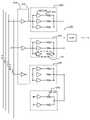
일부 실시예들에서, 개별 드라이버 컴포넌트들을 디스에이블하기 위한 옵션들은, 출력 드라이버 전력/접지 연결들의 제거, 드라이버 출력 연결, 하나 이상의 회로 컴포넌트의 제거 등을 포함한다. 따라서, 레이아웃 대칭 및 일관된 내부 회로 노드 부하를 유지하면서 코드 행렬을 충족시키기 위해 서브채널 또는 와이어 기반으로 기능적 또는 연결된 병렬 드라이버들의 개수가 상이해질 수 있다. 도 4는 와이어 2에 대한 예시적인 와이어 드라이버를 도시한다. 수학식 1에 따르면, 와이어 2는 비트 3 및 비트 4에 따라 변조되는 서브채널들에 의해서만 영향을 받는다. 각 와이어 드라이버 그룹(420, 430, 및 440)은 3개의 드라이버 요소들만을 포함하므로, 비트 3은 드라이버 그룹들(420 및 430)에 연결된 것으로 도시되고, 각 그룹은 2개의 연결된 드라이버 요소들 및 1개의 연결해재된 드라이버 요소를 가지며, 4의 가중치를 제공한다. 비트 4는 드라이버 그룹 440에 연결되어, 3의 가중치를 제공한다.In some embodiments, options for disabling individual driver components include removal of output driver power/ground connections, removal of driver output connection, one or more circuit components, and the like. Thus, the number of functional or connected parallel drivers can be varied on a subchannel or wire basis to satisfy the code matrix while maintaining layout symmetry and consistent internal circuit node loading. 4 shows an exemplary wire driver for wire 2. According to
와이어 0, 와이어 1, 와이어 4, 와이어 5에 대한 제9 드라이버 요소(도 2에서 221로 도시된 연결해재된 드라이버 요소) 및 와이어 2 및 와이어 3에 대한 제8 및 제9 드라이버 요소들은, 원하는 바이어스 또는 공통 모드 신호 레벨을 유지하기 위해, 선택적으로 250으로서 비데이터 구동(즉, 고정 출력) 드라이버 인스턴스로서 인스턴스화될 수 있다. 일부 실시예들에서, 출력 "1"과 출력 "0" 레벨 사이의 중간의 종단 전압이 바람직하며, 따라서 비데이터 구동 인스턴스들은 한 쌍의 드라이버 입력들 중 하나가 하이(high)에 연결되고 다른 하나가 로우(low)에 연결되는 쌍들로 인스턴스화될 수 있다. 홀수의 인스턴스들이 필요하면, 2개의 비데이터 구동 인스턴스들이 상술한 바와 같이 연결될 수 있지만 정상 출력 임피던스의 2배로 되어, 함께 단일 드라이버 부하를 나타낸다. 따라서, 도 2에서 직렬 저항기들(257)은 저항기들(227)의 값의 2배이다. 일부 실시예들에서, 생성되는 공통 모드 전압을 추가로 조정하기 위해 추가의 비데이터 구동 드라이버 인스턴스들이 사용될 수 있다.The ninth driver elements for
도 2에서, 와이어 드라이버 요소들의 컬렉션은 이들 요소들의 병렬 연결(여기서의 예에서와 같이, 와이어 당 9개의 병렬 드라이버들의 깊이)이 송신 라인 임피던스와 동일하면 매칭된 송신 라인 임피던스를 제공할 수 있다. 9개의 병렬 드라이버 요소들 및 50 옴 송신 라인의 이러한 비제한적인 예에서, 각 드라이버 요소가 450 옴의 출력 임피던스를 가질 때 매칭 송신 임피던스가 획득될 것이다. 다른 실시예들에서, 송신 라인 임피던스와 의도적으로 비매칭된 더 높은 드라이버 출력 임피던스가 사용되는데, 여기서 [Amiri I]에서 설명되는 바와 같이, 드라이버 전력 소비가 잠재적인 송신단 신호 반사들보다 큰 염려 사항이다.In FIG. 2, a collection of wire driver elements can provide a matched transmission line impedance if the parallel connection of these elements (as in the example herein, a depth of 9 parallel drivers per wire) equals the transmission line impedance. In this non-limiting example of 9 parallel driver elements and a 50 ohm transmission line, a matching transmit impedance would be obtained when each driver element has an output impedance of 450 ohms. In other embodiments, a higher driver output impedance intentionally mismatched with the transmit line impedance is used, where driver power consumption is a greater concern than potential transmit end signal reflections, as described in [Amiri I]. .
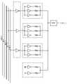
도 3 내지 도 7은 와이어 0 내지 와이어 5를 구동하기 위한 유사한 멀티레벨 드라이버의 실시예들을 도시하는데, 각 드라이버는 (i) 수신된 한 세트의 데이터 비트들 중 서브세트의 데이터 비트들, (ii) 각 데이터 비트에 대한 인버팅/비인버팅 버퍼링, 및 각 서브채널 컴포넌트 또는 비데이터 구동 바이어스 컴포넌트에 대해 얼마나 많은 드라이버 인스턴스들이 사용되는지에 대한 개개의 구성들을 갖는다.3-7 show embodiments of similar multilevel drivers for driving
도 1 내의 라인 드라이버(118)는 도 2 내지 도 7에 도시된 와이어 드라이버들의 집합적인 배열 형태를 취할 수 있으며, [Shokrollahi I]의 5b6w-10 벡터 시그널링 코드에 대한 완전한 6 와이어 출력 드라이버의 실시예를 나타낸다. 도 10은 일부 실시예들에 따른 방법(1000)의 흐름도이다. 도시된 바와 같이, 방법(1000)은 복수의 드라이버들에서 한 세트의 입력 비트들을 수신하는 단계(1002)를 포함하며, 하나의 그러한 드라이버가 도 2의 개략도에 의해 도시된다. 각 드라이버는 한 세트의 입력 비트들 중 서브세트의 입력 비트들을 수신(1004)하는데, 수신된 서브세트의 비트들은 개개의 와이어와 연관된 서브채널들에 대응한다. 각 드라이버는 복수의 가중 아날로그 신호 컴포넌트들을 생성(1006)하는데, 각 가중 아날로그 신호 컴포넌트는 (i) 개개의 와이어와 연관된 한 세트의 와이어 특유의 서브채널 가중치들로부터 선택된 대응하는 가중치 및 부호를 가지며 (ii) 수신된 서브세트의 비트들의 대응하는 비트에 의해 변조된다. 도 2에 도시된 바와 같이, 각각의 서브채널 드라이버 요소 그룹(220, 230, 및 240)은 개개의 가중 아날로그 신호 컴포넌트를 생성하는데, 가중치의 크기는 인에이블된 드라이버 요소들의 개수(서브채널 드라이버 요소 그룹(220)의 경우에 3개)에 의해 결정되며, 210에서 버퍼링 요소에 의해 부여되는 부호는 반전 또는 비반전이다. 세트들의 와이어 특유의 서브채널 컴포넌트들의 크기들 및 부호들은 수학식 1의 행렬의 열들에 따라 결정될 수 있다. 예를 들어, 와이어 wO에 대해, 한 세트의 와이어 특유의 서브채널 컴포넌트들은 행렬의 제1 열 3, 2, 및 -3(스케일링 계수 1/3 없이 및 공통 모드 행 제외)에 대응한다. 각 서브채널 컴포넌트의 크기는, 서브채널 컴포넌트에 대해 얼마나 많은 드라이버 요소들이 인에이블되는지를 결정하는 한편, 각 서브채널 컴포넌트의 부호는, 서브채널 컴포넌트를 변조하는 대응하는 비트에 비반전(양의 부호) 또는 반전(음의 부호) 버퍼가 적용되는지를 결정한다. 신호들의 앙상블의 개개의 신호가 개개의 와이어에 연결된 공통 노드(225)에서 복수의 가중 아날로그 신호 컴포넌트들의 합산을 형성함으로써 생성되며(1008), 개개의 신호는 멀티 와이어 버스의 개개의 와이어를 통해 응답적으로 송신된다(1010).
일부 실시예들에서, 신호들의 앙상블은 벡터 시그널링 코드의 코드워드를 나타낸다.In some embodiments, the ensemble of signals represents a codeword of a vector signaling code.
일부 실시예들에서, 각각의 가중 아날로그 신호 컴포넌트를 생성하는 단계는, 서브채널 드라이버 요소 그룹의 하나 이상의 드라이버 요소를 개개의 와이어에 병렬로 연결하는 단계를 포함한다. 도 2에서, 서브채널 드라이버 요소 그룹 2는, 3개의 드라이버 요소들이 공통 노드(225)에 연결되므로, 비트 2에 '3'의 가중치를 적용함으로써 가중 아날로그 신호 컴포넌트를 생성하는 한편, 서브채널 드라이버 요소 그룹 2는, 2개의 드라이버 요소들이 공통 노드(225)에 연결되므로, 비트 3에 '2'의 가중치를 적용함으로써 가중 아날로그 신호 컴포넌트를 생성한다. 도시된 바와 같이, 210에서의 버퍼링 요소들 둘 다는 비트 2 및 비트 3에 대해 비반전이다. 서브채널 드라이버 요소 그룹(240)은, 공통 노드(225)에 연결된 3개의 드라이버 요소들이 있고 210에서의 비트 4에 대한 버퍼링 스테이지가 반전되므로, 비트 4에 '-3'의 가중치를 적용함으로써 가중 아날로그 신호 컴포넌트를 생성한다. 따라서, 가중 아날로그 신호 컴포넌트의 대응하는 가중치는 서브채널 드라이버 요소 그룹 내의 연결된 드라이버 요소들의 개수에 대응한다.In some embodiments, generating each weighted analog signal component includes connecting one or more driver elements of a group of sub-channel driver elements in parallel to a respective wire. In FIG. 2, since the three driver elements are connected to the
일부 실시예들에서, 복수의 멀티레벨 드라이버들의 각 멀티레벨 드라이버는 동일한 총 개수의 드라이버 요소들을 갖는다. 도 2 내지 도 7에서, 각 멀티레벨 드라이버는, 구현 대칭을 유지하기 위한 추가 그룹(예를 들면, 250)의 2개의 드라이버 요소들 뿐만 아니라 서브채널 드라이버 요소 그룹들 전반에 걸친 9개의 총 드라이버 요소을 포함한다.In some embodiments, each multilevel driver of the plurality of multilevel drivers has the same total number of driver elements. 2-7, each multilevel driver includes two driver elements in an additional group (e.g., 250) to maintain implementation symmetry, as well as nine total driver elements across subchannel driver element groups. include
일부 실시예들에서, 복수의 멀티레벨 드라이버들의 제1 멀티레벨 드라이버 내의 연결된 드라이버 요소들의 총 개수는 복수의 멀티레벨 드라이버들의 제2 멀티레벨 드라이버 내의 연결된 드라이버의 총 개수와 상이하다. 예를 들어, 도 2에 도시된 와이어 0에 연결된 멀티레벨 드라이버는 연결된 8개의 드라이버 요소들을 갖는 한편, 도 4에 도시된 와이어 2에 연결된 멀티레벨 드라이버는 공통 노드에 연결된 7개의 드라이버 요소들을 갖는다.In some embodiments, a total number of connected driver elements in a first multilevel driver of the plurality of multilevel drivers is different from a total number of connected drivers in a second multilevel driver of the plurality of multilevel drivers. For example, the multilevel driver connected to
일부 실시예들에서, 서브채널 드라이버 요소 그룹 내의 각 드라이버 요소는 멀티 와이어 버스의 개개의 와이어로부터의 전류를 소싱(sourcing) 또는 싱킹(sinking)함으로써 개개의 와이어의 전압을 조정하기 위한 푸시-풀 드라이버를 포함한다.In some embodiments, each driver element in a group of sub-channel driver elements is a push-pull driver for regulating the voltage of an individual wire by sourcing or sinking current from the individual wire of the multi-wire bus. includes
일부 실시예들에서, 방법은 서브세트의 비트들의 각 입력 비트에 대해, 대응하는 부호에 따라 대응하는 입력 비트를 반전시키거나 반전시키지 않는 단계를 포함한다. 그러한 반전은 수학식 1의 행렬에서 서브채널 특정 가중치들의 부호들에 의해 결정되는 반전 및/또는 비반전 버퍼링 요소들의 조합을 갖는 비트 사이너(bit signer)(210)에 의해 수행된다.In some embodiments, the method includes for each input bit of the subset of bits, inverting or not inverting the corresponding input bit according to a corresponding sign. Such inversion is performed by a
일부 실시예들에서, 방법은 세트들의 비트의 복수의 위상들을 수신하는 단계 및 클록 선택 신호에 따라 한 세트의 입력 비트들을 응답적으로 선택하는 단계를 더 포함한다. 그러한 실시예는 도 9에 도시된 멀티플렉싱 구조를 이용할 수 있다.In some embodiments, the method further includes receiving the plurality of phases of the sets of bits and responsively selecting the set of input bits in accordance with the clock selection signal. Such an embodiment may use the multiplexing structure shown in FIG. 9 .
일부 실시예들에서, 각 세트의 와이어 특유의 서브채널 가중치들은 직교 행렬의 행에 대응하고, 직교 행렬의 각 행은 상호 직교(mutually-orthogonal)한다. 그러한 행렬은 수학식 1에 주어진다. 일부 실시예들에서, 직교 행렬은 등안(equal-eye) 행렬이다.In some embodiments, the wire-specific subchannel weights of each set correspond to a row of an orthogonal matrix, and each row of the orthogonal matrix is mutually-orthogonal. Such a matrix is given in
일부 실시예들에서, 복수의 서브채널들은 동기적으로 변조될 수 있으며, 생성된 신호들의 앙상블은 벡터 시그널링 코드의 코드워드에 대응한다. 대안적으로, 각 서브채널은 비동기적으로 변조될 수 있으며, 각 비트는 따라서 멀티 와이어 버스를 통해 비동기적으로 송신된다.In some embodiments, multiple subchannels may be synchronously modulated, and the ensemble of generated signals corresponds to a codeword of a vector signaling code. Alternatively, each subchannel can be modulated asynchronously, and each bit is thus transmitted asynchronously over the multi-wire bus.
한 세트의 입력 비트들은 제한적이지 않고 따라서 임의의 값을 취할 수 있으며, 각각의 그러한 세트의 입력 비트들은 본질적으로 각 단위 간격에서 송신의 집단적 상태를 나타내는 고유하고 반복 가능한 출력 결과를 생성하며, 따라서 설명된 실시예는 벡터 시그널링 코드의 모든 코드워드를 기능적으로 재현할 수 있다.A set of input bits is not limiting and can thus take on any value, with each such set of input bits essentially producing a unique and repeatable output result representing the collective state of transmission at each unit interval, thus describing This embodiment can functionally reproduce all codewords of the vector signaling code.
[Ulrich I]에 의해 설명되는 바와 같은 코드워드 인코더와 멀티레벨 출력 드라이버의 조합과 비교하면 명백한 바와 같이, 본 실시예는 덜 복잡하고 잠재적으로는 집적 회로 설계로서 레이아웃하기에 용이하다. 간단한 인버터/비인버터 데이터 버퍼 로직은 코드워드 인코더를 구현하는 데 사용되는 불 로직(Boolean logic)보다 훨씬 덜 복잡하며, 이진 데이터 비트들은 인코딩된 코드워드 심벌들보다 훨씬 작은 신호 라우팅 복잡도를 도입한다.As is evident in comparison to the combination of a codeword encoder and multilevel output driver as described by [Ulrich I], this embodiment is less complex and potentially easier to lay out as an integrated circuit design. The simple inverter/non-inverter data buffer logic is much less complex than the Boolean logic used to implement the codeword encoder, and binary data bits introduce much less signal routing complexity than encoded codeword symbols.
설명된 예들에서 각 와이어 드라이버 내의 드라이버 요소들/슬라이스들의 개수, 와이어들의 개수, 및 비트들의 개수는 제한적인 것으로 간주되어서는 안됨에 유의해야 한다. 비트들의 상이한 조합들/가중치들 뿐만 아니라, 다른 개수의 드라이버 요소들이 각 와이어 드라이버에 사용될 수 있다.It should be noted that the number of driver elements/slices, number of wires, and number of bits in each wire driver in the described examples should not be considered limiting. Different combinations/weights of bits, as well as different numbers of driver elements can be used for each wire driver.
추가 드라이버 인스턴스들Additional Driver Instances
[Ulrich I]에서 설명되는 바와 같이, 보다 적은 수의 보다 낮은 임피던스 출력 드라이버들에 비해, 병렬로 고 임피던스 출력 드라이버들 또는 "슬라이스들"의 보다 많은 인스턴스들을 사용하는 것으로부터 상당한 구현의 이점이 있을 수 있으며, 본 실시예는 그러한 조합에 도움이 된다.As described in [Ulrich I], there will be significant implementation benefit from using more instances of high-impedance output drivers or “slices” in parallel, compared to a smaller number of lower-impedance output drivers. can, and this embodiment is conducive to such a combination.
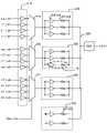
도 8은 도 2의 서브채널 드라이버 요소 그룹(220)과 기능적으로는 동등하지만 내부적으로 3개의 세트들의 드라이버 요소 인스턴스들(810, 820, 및 830)을 포함하는 드라이버 요소의 일 실시예를 도시한다. 810 내에서, 각 직렬 저항기(827)는 도 2의 직렬 저항기(227)의 저항의 3배의 저항을 가지며, 각 드라이버 요소(822)는 도 2의 드라이버 요소(222)의 1/3의 전류를 처리한다. 전술한 공통 레이아웃 모듈 모델에 따라, 이 기법을 도 2의 설계에 적용하는 실시예는, 도 2의 220, 230, 240, 및 선택적으로 250 각각을 도 8의 설계로 대체하게 되는데, 이들 대체는 활성 대(vs) 디스에이블된 드라이버 인스턴스들의 개수만 상이하다. 다른 실시예들은 이 예의 3개의 인스턴스들(820)에 비해, 더 적거나 더 많은 개수의 병렬 드라이버들을 이용할 수 있다. 일부 실시예들에서, "슬라이스"는 예를 들면, 도 2에 도시된 바와 같은 전체 구조물에 대응할 수 있으며, 복수의 그러한 "슬라이스들"은 와이어 0에 대해 병렬로 배열될 수 있다.FIG. 8 shows one embodiment of a driver element that is functionally equivalent to subchannel
다상 데이터 처리와의 통합Integration with multiphase data processing
이러한 고속으로의 데이터의 처리를 용이하게 하기 위해 다수의 본질적으로 병렬인 데이터 처리 인스턴스들을 통합하는 것이 일반적인 관행이다. [Shokrollahi I] 및 [Ulrich I]은 예들로서, 4개보다 많은 병렬 처리 인스턴스들을 갖는 실시예들을 설명한다.It is common practice to incorporate multiple essentially parallel instances of data processing to facilitate processing of data at such high speeds. [Shokrollahi I] and [Ulrich I] describe embodiments with more than four instances of parallel processing as examples.
도 9의 드라이버는, 송신될 데이터가 4개의 본질적으로 병렬인 처리 위상들로부터 얻어진다는 것을 제외하고, 도 2의 드라이버와 동일하다. 따라서, 데이터 버퍼(910)는, 각각이 상이한 데이터 처리 위상으로부터 동일한 데이터 비트들을 취출하는, 각 입력 비트에 대한 4개의 동일한 버퍼링 인스턴스들을 포함한다. 4상 클록들(four-phase clock)(Clk4 <3:0>)에 의해 제어되는 디지털 멀티플렉서들(915, 916, 및 917)이 각 위상으로부터 데이터를 순차적으로 선택하여, 4 배의 속도로 단일 출력 스트림을 생성한다. 이전 예에서와 같이, 데이터 위상들의 개수와 데이터 멀티플렉서들의 위치는 설명의 명료성을 위해 선택되었으며, 제한을 시사하지 않는다.The driver of Fig. 9 is identical to the driver of Fig. 2, except that the data to be transmitted is obtained from four essentially parallel phases of processing. Thus,
유사하게, 동일한 클록이 디지털 멀티플렉서들(915, 916, 및 917)을 본질적으로 병렬로 제어하는 것으로 도시되어 있으나, 다른 실시예들은 예를 들면, 위상 지연 요소들 또는 위상 보간기(phase interpolator)를 사용하여 상이한 타이밍 지연들을 도입할 수 있어서, 상이한 서브채널 결과들 또는 조합된 와이어 결과가 상이한 시간들에 변경되도록 할 수 있다. 추가의 실시예들은 이 등시성 클록 거동(isochronous clock behavior)을 넘어서, 서브채널들 중 하나 이상이 비동기적으로 전이하도록 할 수 있다.Similarly, while the same clock is shown controlling
다수의 데이터 소스 위상들로부터 또는 실제로 보다 넓고 보다 저속의 인터페이스 또는 버퍼링 매체로부터의 데이터를 조합하는 이러한 접근법은, 제한없이 본원에서 설명된 다른 요소들 또는 다른 공지된 기술 접근법들과 조합하여 사용될 수 있다.This approach of combining data from multiple data source topologies, or indeed wider and slower interfaces or buffering media, may be used in combination with other known technology approaches or other elements described herein without limitation. .
Claims (20)
Translated fromKorean일 세트의 입력 비트들을 수신하고 벡터 시그널링 코드의 코드워드(codeword)의 심벌(symbol)들에 대응하는 일 세트의 신호들을 응답적으로(responsively) 생성하도록 구성된 복수의 멀티 레벨 드라이버(multi-level driver)들을 포함하고, 상기 복수의 멀티 레벨 드라이버들 중 각각의 멀티 레벨 드라이버는, 멀티 와이어 버스(multi-wire bus)의 개개의 와이어에 연결되고 상기 일 세트의 신호들의 개개의 신호를 생성하도록 구성되며, 각각의 멀티 레벨 드라이버는:
상기 일 세트의 입력 비트들 중 일 서브세트의 입력 비트들을 수신하도록 구성된 데이터 버퍼 - 상기 일 세트의 입력 비트들 중 수신된 상기 서브세트의 입력 비트들은 상기 개개의 와이어와 연관된 서브채널들에 대응하고, 상기 데이터 버퍼는 상기 일 세트의 입력 비트들 중 상기 서브세트의 입력 비트들의 각각의 입력 비트에 개개의 부호(sign)를 적용함으로써 개개의 세트의 부호화된 입력 비트들을 생성하도록 구성되며, 상기 개개의 부호는 개개의 와이어 특유의 서브채널 가중치에 의해 결정됨 - ;
복수의 가중 아날로그 신호 컴포넌트(weighted analog signal component)들을 생성하도록 구성된 복수의 서브채널 드라이버 요소 그룹들 - 각각의 서브채널 드라이버 요소 그룹은 상기 개개의 세트의 부호화된 입력 비트들 중 개개의 부호화된 입력 비트를 받아들이도록, 그리고 상기 서브채널 드라이버 요소 그룹에 병렬로 연결된 인에이블된 드라이버 요소들의 개수에 의해 결정되는 크기를 갖는 개개의 가중 아날로그 신호 컴포넌트를 생성하도록 구성됨 - ; 및
상기 개개의 와이어에 연결된 합산(summation) 노드 - 상기 합산 노드는 상기 복수의 가중 아날로그 신호 컴포넌트들의 합산을 형성함으로써 상기 개개의 와이어를 통해 전송하기 위해 상기 일 세트의 신호들의 개개의 신호를 생성하도록 구성됨 -
를 포함하는 것인, 장치.In the device,
A plurality of multi-level drivers configured to receive a set of input bits and responsively generate a set of signals corresponding to symbols of a codeword of a vector signaling code. ), wherein each multi-level driver of the plurality of multi-level drivers is connected to a respective wire of a multi-wire bus and is configured to generate a respective signal of the set of signals; , each multi-level driver:
a data buffer configured to receive a subset of the input bits of the set of input bits, wherein the received input bits of the set of input bits correspond to subchannels associated with the respective wire; , wherein the data buffer is configured to generate a respective set of coded input bits by applying a respective sign to each input bit of the subset of input bits of the set of input bits; The sign of - is determined by the subchannel weight specific to each wire;
A plurality of groups of sub-channel driver elements configured to generate a plurality of weighted analog signal components, each group of sub-channel driver elements comprising a respective coded input bit of the respective set of coded input bits. ; and
a summation node coupled to the respective wire, the summation node configured to generate a respective signal of the set of signals for transmission over the respective wire by forming a summation of the plurality of weighted analog signal components. -
A device comprising a.
상기 데이터 버퍼는 상기 개개의 세트의 부호화된 입력 비트들을 생성하기 위해 상기 일 세트의 입력 비트들 중 상기 수신된 서브세트의 하나 이상의 입력 비트를 반전시키도록 구성된 로직 인버터들을 포함하는 것인, 장치.According to claim 1,
wherein the data buffer comprises logic inverters configured to invert one or more input bits of the received subset of the set of input bits to produce the respective set of coded input bits.
상기 복수의 서브채널 드라이버 요소 그룹들 중 각각의 서브채널 드라이버 요소 그룹은 동일한 개수의 인에이블된 드라이버 요소들을 포함하는 것인, 장치.According to claim 1,
wherein each sub-channel driver element group of the plurality of groups of sub-channel driver elements includes the same number of enabled driver elements.
상기 복수의 서브채널 드라이버 요소 그룹들 중 적어도 하나의 서브채널 드라이버 요소 그룹은 적어도 하나의 디스에이블된 드라이버 요소를 포함하는 것인, 장치.According to claim 1,
wherein at least one sub-channel driver element group of the plurality of groups of sub-channel driver elements includes at least one disabled driver element.
상기 복수의 서브채널 드라이버 요소 그룹들 중 적어도 두개의 서브채널 드라이버 요소 그룹들은 상이한 개수의 인에이블된 드라이버 요소들을 포함하는 것인, 장치.According to claim 1,
wherein at least two sub-channel driver element groups of the plurality of sub-channel driver element groups include different numbers of enabled driver elements.
상기 인에이블된 드라이버 요소들은 상기 합산 노드로부터의 전류를 소싱(source) 또는 싱킹(sink)하도록 구성된 푸시-풀 드라이버(push-pull driver)들을 포함하는 것인, 장치.According to claim 1,
wherein the enabled driver elements comprise push-pull drivers configured to source or sink current from the summation node.
상기 벡터 시그널링 코드는 직교 차분 벡터 시그널링(Orthogonal Differential Vector Signaling; ODVS) 코드인 것인, 장치.According to claim 1,
The vector signaling code is an orthogonal differential vector signaling (ODVS) code.
상기 ODVS 코드는 등안(equal-eye) ODVS 코드인 것인, 장치.According to claim 7,
Wherein the ODVS code is an equal-eye ODVS code.
적어도 하나의 멀티 레벨 드라이버는 상기 일 세트의 입력 비트들의 모든 입력 비트들에 대응하는 상기 일 세트의 입력 비트들 중 일 서브세트의 입력비트들을 수신하는 것인, 장치.According to claim 1,
wherein at least one multi-level driver receives a subset of the input bits of the set of input bits corresponding to all input bits of the set of input bits.
상기 복수의 멀티 레벨 드라이버들 중 적어도 두개의 멀티 레벨 드라이버들은 상기 일 세트의 입력 비트들 중 상이한 개수의 입력 비트들을 갖는 상기 일 세트의 입력 비트들 중 대응 서브세트들의 입력 비트들을 수신하는 것인, 장치.According to claim 1,
wherein at least two multi-level drivers of the plurality of multi-level drivers receive input bits of corresponding subsets of the set of input bits having different numbers of input bits of the set of input bits; Device.
일 세트의 입력 비트들을 수신하고 벡터 시그널링 코드의 코드워드(codeword)의 심벌(symbol)들에 대응하는 일 세트의 신호들을 응답적으로(responsively) 생성하도록 구성된 복수의 멀티 레벨 드라이버(multi-level driver)들 중의 멀티 레벨 드라이버에서, 상기 일 세트의 입력 비트들 중 일 서브세트의 입력 비트들을 수신하는 단계 - 상기 수신된 서브세트의 입력 비트들은 멀티 와이어 버스(multi-wire bus)의 개개의 와이어와 연관된 서브 채널들에 대응함 - ;
상기 일 세트의 입력 비트들 중 일 서브세트의 각각의 입력 비트에 개개의 부호(sign)를 적용함으로써 데이터 버퍼를 사용하여 일 세트의 부호화된 입력 비트들을 생성하는 단계 - 상기 개개의 부호는 개개의 와이어 특유의 서브채널 가중치에 의해 결정됨 - ;
상기 일 세트의 부호화된 입력 비트들을 받아들이는 복수의 서브채널 드라이버 요소 그룹들을 사용하여 복수의 가중 아날로그 신호 컴포넌트(weighted analog signal component)들을 생성하는 단계 - 각각의 서브채널 드라이버 요소 그룹은 상기 일 세트의 부호화된 입력 비트들 중 개개의 부호화된 입력 비트를 받아들이도록, 그리고 상기 서브채널 드라이버 요소 그룹내의 인에이블된 드라이버 요소들의 개수에 의해 결정되는 크기를 갖는 개개의 가중 아날로그 신호 컴포넌트를 생성하도록 구성됨 - ; 및
상기 복수의 가중 아날로그 신호 컴포넌트들의 아날로그 합산(summation)을 형성함으로써, 상기 개개의 와이어에 연결된 합산 노드를 사용하여 상기 개개의 와이어를 통해 전송하기 위한 신호를 생성하는 단계
를 포함하는 것인, 방법.in the method,
A plurality of multi-level drivers configured to receive a set of input bits and responsively generate a set of signals corresponding to symbols of a codeword of a vector signaling code. ) of the multi-level driver, receiving a subset of the input bits of the set of input bits, wherein the input bits of the received subset correspond to individual wires of a multi-wire bus. corresponding to associated sub-channels;
generating a set of coded input bits using a data buffer by applying a respective sign to each input bit of a subset of the set of input bits, wherein the respective signs are -Determined by wire-specific subchannel weights;
generating a plurality of weighted analog signal components using a plurality of groups of sub-channel driver elements that accept the set of coded input bits, each group of sub-channel driver elements of the set of configured to accept an individual coded input bit of the coded input bits and to generate a respective weighted analog signal component having a magnitude determined by the number of enabled driver elements in the group of sub-channel driver elements; and
generating an analog summation of the plurality of weighted analog signal components, thereby generating a signal for transmission over the respective wire using a summation node coupled to the respective wire.
To include, the method.
상기 일 세트의 부호화된 입력 비트들을 생성하는 단계는 상기 일 세트의 입력 비트들 중 수신된 서브세트의 하나 이상의 입력 비트를 논리적으로 반전시키는 단계를 포함하는 것인, 방법.According to claim 11,
wherein generating the set of coded input bits comprises logically inverting one or more input bits of a received subset of the set of input bits.
상기 복수의 서브채널 드라이버 요소 그룹들은 상기 멀티 와이어 버스의 제2 와이어와 연관된 제2 복수의 서브채널 드라이버 요소 그룹들과 동일한 개수의 인에이블된 드라이버 요소들을 포함하는 것인, 방법.According to claim 11,
wherein the plurality of groups of sub-channel driver elements includes the same number of enabled driver elements as the second plurality of groups of sub-channel driver elements associated with a second wire of the multi-wire bus.
상기 복수의 서브채널 드라이버 요소 그룹들 중 적어도 하나의 서브채널 드라이버 요소 그룹은 적어도 하나의 디스에이블된 드라이버 요소를 포함하는 것인, 방법.According to claim 11,
wherein at least one sub-channel driver element group of the plurality of groups of sub-channel driver elements includes at least one disabled driver element.
상기 복수의 서브채널 드라이버 요소 그룹들 중 적어도 두개의 서브채널 드라이버 요소 그룹들은 상이한 개수의 인에이블된 드라이버 요소들을 포함하는 것인, 방법.According to claim 11,
wherein at least two sub-channel driver element groups of the plurality of sub-channel driver element groups include different numbers of enabled driver elements.
상기 가중 아날로그 신호 컴포넌트들을 생성하는 단계는 푸시-풀 드라이버(push-pull driver)들을 사용하여 상기 인에이블된 드라이버 요소들이 상기 합산 노드로부터의 전류를 소싱(sourcing) 또는 싱킹(sinking)하는 단계를 포함하는 것인, 방법.According to claim 11,
generating the weighted analog signal components comprises sourcing or sinking current from the summing node with the enabled driver elements using push-pull drivers; How to do it.
상기 벡터 시그널링 코드는 직교 차분 벡터 시그널링(Orthogonal Differential Vector Signaling; ODVS) 코드인 것인, 방법.According to claim 11,
The vector signaling code is an orthogonal differential vector signaling (ODVS) code.
상기 ODVS 코드는 등안(equal-eye) ODVS 코드인 것인, 방법.According to claim 17,
Wherein the ODVS code is an equal-eye ODVS code.
상기 일 세트의 입력 비트들 중 일 서브세트의 입력 비트들은 상기 일 세트의 입력 비트들의 모든 입력 비트들에 대응하는 것인, 방법.According to claim 11,
wherein input bits of a subset of the set of input bits correspond to all input bits of the set of input bits.
상기 복수의 멀티 레벨 드라이버들 중 적어도 두개의 멀티 레벨 드라이버들은 상기 일 세트의 입력 비트들 중 상이한 개수의 입력 비트들을 갖는 상기 일 세트의 입력 비트들 중 대응 서브세트들의 입력 비트들을 수신하는 것인, 방법.
According to claim 11,
wherein at least two multi-level drivers of the plurality of multi-level drivers receive input bits of corresponding subsets of the set of input bits having different numbers of input bits of the set of input bits; Way.
Applications Claiming Priority (4)
| Application Number | Priority Date | Filing Date | Title |
|---|---|---|---|
| US15/698,567US10496583B2 (en) | 2017-09-07 | 2017-09-07 | Low power multilevel driver for generating wire signals according to summations of a plurality of weighted analog signal components having wire-specific sub-channel weights |
| US15/698,567 | 2017-09-07 | ||
| KR1020207009352AKR102386885B1 (en) | 2017-09-07 | 2018-09-06 | Low Power Multilevel Driver |
| PCT/US2018/049805WO2019051129A1 (en) | 2017-09-07 | 2018-09-06 | Low power multilevel driver |
Related Parent Applications (1)
| Application Number | Title | Priority Date | Filing Date |
|---|---|---|---|
| KR1020207009352ADivisionKR102386885B1 (en) | 2017-09-07 | 2018-09-06 | Low Power Multilevel Driver |
Publications (2)
| Publication Number | Publication Date |
|---|---|
| KR20220048061A KR20220048061A (en) | 2022-04-19 |
| KR102486476B1true KR102486476B1 (en) | 2023-01-09 |
Family
ID=65517599
Family Applications (2)
| Application Number | Title | Priority Date | Filing Date |
|---|---|---|---|
| KR1020207009352AActiveKR102386885B1 (en) | 2017-09-07 | 2018-09-06 | Low Power Multilevel Driver |
| KR1020227012021AActiveKR102486476B1 (en) | 2017-09-07 | 2018-09-06 | Low power multilevel driver |
Family Applications Before (1)
| Application Number | Title | Priority Date | Filing Date |
|---|---|---|---|
| KR1020207009352AActiveKR102386885B1 (en) | 2017-09-07 | 2018-09-06 | Low Power Multilevel Driver |
Country Status (5)
| Country | Link |
|---|---|
| US (2) | US10496583B2 (en) |
| EP (1) | EP3679654B1 (en) |
| KR (2) | KR102386885B1 (en) |
| CN (2) | CN114328338B (en) |
| WO (1) | WO2019051129A1 (en) |
Families Citing this family (8)
| Publication number | Priority date | Publication date | Assignee | Title |
|---|---|---|---|---|
| US10365833B2 (en)* | 2016-01-22 | 2019-07-30 | Micron Technology, Inc. | Apparatuses and methods for encoding and decoding of signal lines for multi-level communication architectures |
| CN112217755B (en)* | 2019-07-11 | 2023-11-03 | 默升科技集团有限公司 | Parallel channel skew for enhanced error correction |
| CN113839654A (en)* | 2020-06-23 | 2021-12-24 | 深圳市中兴微电子技术有限公司 | Multi-level output driving circuit and method |
| US11695596B2 (en)* | 2021-04-19 | 2023-07-04 | Realtek Semiconductor Corp. | Multi-level signal transmitter and method thereof |
| US11831472B1 (en)* | 2022-08-30 | 2023-11-28 | Kandou Labs SA | Pre-scaler for orthogonal differential vector signalling |
| US12063034B2 (en) | 2022-08-30 | 2024-08-13 | Kandou Labs SA | Line driver impedance calibration for multi-wire data bus |
| WO2024124046A1 (en) | 2022-12-09 | 2024-06-13 | Kandou Labs SA | Bidirectional orthogonal differential vector signaling |
| US12424265B2 (en)* | 2023-04-17 | 2025-09-23 | Qualcomm Incorporated | Chip select transmitters for multiple signal levels |
Citations (2)
| Publication number | Priority date | Publication date | Assignee | Title |
|---|---|---|---|---|
| US20160013954A1 (en) | 2014-07-10 | 2016-01-14 | Kandou Labs S.A. | Vector Signaling Codes with Increased Signal to Noise Characteristics |
| US20170147520A1 (en) | 2015-11-25 | 2017-05-25 | Kandou Labs S.A. | Orthogonal differential vector signaling codes with embedded clock |
Family Cites Families (45)
| Publication number | Priority date | Publication date | Assignee | Title |
|---|---|---|---|---|
| CA2109634C (en)* | 1991-05-24 | 2001-07-24 | Ugo O. Gagliardi | Isdn interfacing of personal computers |
| US5539360A (en) | 1994-03-11 | 1996-07-23 | Motorola, Inc. | Differential transmission line including a conductor having breaks therein |
| US6172634B1 (en) | 1998-02-25 | 2001-01-09 | Lucent Technologies Inc. | Methods and apparatus for providing analog-fir-based line-driver with pre-equalization |
| TW440767B (en) | 1998-06-02 | 2001-06-16 | Fujitsu Ltd | Method of and apparatus for correctly transmitting signals at high speed without waveform distortion |
| US6288089B1 (en) | 1998-12-21 | 2001-09-11 | Michael Zawada | Use of kinase inhibitors for treating neurodegenerative diseases |
| US6697420B1 (en) | 1999-05-25 | 2004-02-24 | Intel Corporation | Symbol-based signaling for an electromagnetically-coupled bus system |
| US6496889B1 (en) | 1999-09-17 | 2002-12-17 | Rambus Inc. | Chip-to-chip communication system using an ac-coupled bus and devices employed in same |
| US7269212B1 (en) | 2000-09-05 | 2007-09-11 | Rambus Inc. | Low-latency equalization in multi-level, multi-line communication systems |
| US7124221B1 (en) | 1999-10-19 | 2006-10-17 | Rambus Inc. | Low latency multi-level communication interface |
| DE10016445C2 (en) | 2000-03-29 | 2002-03-28 | Infineon Technologies Ag | Electronic output stage |
| DE10249016B4 (en) | 2002-10-21 | 2006-10-19 | Infineon Technologies Ag | Multi-level driver stage |
| US7176823B2 (en) | 2002-11-19 | 2007-02-13 | Stmicroelectronics, Inc. | Gigabit ethernet line driver and hybrid architecture |
| US7126378B2 (en) | 2003-12-17 | 2006-10-24 | Rambus, Inc. | High speed signaling system with adaptive transmit pre-emphasis |
| KR100976489B1 (en)* | 2003-10-01 | 2010-08-18 | 엘지전자 주식회사 | Control method of data modulation and coding method applied to multi-input multi-output system of mobile communication |
| US7639746B2 (en) | 2005-07-01 | 2009-12-29 | Apple Inc. | Hybrid voltage/current-mode transmission line driver |
| KR100790968B1 (en) | 2005-08-10 | 2008-01-02 | 삼성전자주식회사 | Input and output driver circuits for differential signal transmission, differential signal transmission device and method therewith |
| US7570704B2 (en) | 2005-11-30 | 2009-08-04 | Intel Corporation | Transmitter architecture for high-speed communications |
| US7439761B2 (en) | 2006-07-12 | 2008-10-21 | Infineon Technologies Ag | Apparatus and method for controlling a driver strength |
| US7372295B1 (en) | 2006-12-22 | 2008-05-13 | Altera Corporation | Techniques for calibrating on-chip termination impedances |
| US7462956B2 (en) | 2007-01-11 | 2008-12-09 | Northrop Grumman Space & Mission Systems Corp. | High efficiency NLTL comb generator using time domain waveform synthesis technique |
| US8102934B2 (en)* | 2007-08-16 | 2012-01-24 | Samsung Electronics Co., Ltd. | Transmitting apparatus and method |
| JP5465376B2 (en)* | 2007-10-18 | 2014-04-09 | ピーエスフォー ルクスコ エスエイアールエル | Semiconductor device and driver control method |
| CN101478286A (en) | 2008-03-03 | 2009-07-08 | 锐迪科微电子(上海)有限公司 | Square wave-sine wave signal converting method and converting circuit |
| US7859356B2 (en) | 2008-03-21 | 2010-12-28 | Qualcomm Incorporated | Transmission line system having high common mode impedance |
| US7646215B2 (en) | 2008-03-24 | 2010-01-12 | Sony Corporation | Efficient method for implementing programmable impedance output drivers and programmable input on die termination on a bi-directional data bus |
| JP4958849B2 (en) | 2008-06-19 | 2012-06-20 | パナソニック株式会社 | Differential transmission line |
| KR101173942B1 (en) | 2008-11-28 | 2012-08-14 | 한국전자통신연구원 | Data transmission device, data receiving device, data transmitting system and method for transmitting data |
| KR101079603B1 (en) | 2009-08-11 | 2011-11-03 | 주식회사 티엘아이 | Differential Data Transmitting and Receiving Device and Method with using 3 level volatge |
| US8295336B2 (en) | 2010-03-16 | 2012-10-23 | Micrel Inc. | High bandwidth programmable transmission line pre-emphasis method and circuit |
| US9288089B2 (en)* | 2010-04-30 | 2016-03-15 | Ecole Polytechnique Federale De Lausanne (Epfl) | Orthogonal differential vector signaling |
| US9362962B2 (en) | 2010-05-20 | 2016-06-07 | Kandou Labs, S.A. | Methods and systems for energy-efficient communications interface |
| JP5330359B2 (en) | 2010-11-19 | 2013-10-30 | 株式会社東芝 | High frequency circuit |
| JP5623883B2 (en) | 2010-11-29 | 2014-11-12 | ルネサスエレクトロニクス株式会社 | Differential amplifier and data driver |
| US8520348B2 (en) | 2011-12-22 | 2013-08-27 | Lsi Corporation | High-swing differential driver using low-voltage transistors |
| US8717215B2 (en) | 2012-05-18 | 2014-05-06 | Tensorcom, Inc. | Method and apparatus for improving the performance of a DAC switch array |
| US8975948B2 (en) | 2012-11-15 | 2015-03-10 | Texas Instruments Incorporated | Wide common mode range transmission gate |
| US9048824B2 (en) | 2012-12-12 | 2015-06-02 | Intel Corporation | Programmable equalization with compensated impedance |
| WO2014124450A1 (en) | 2013-02-11 | 2014-08-14 | Kandou Labs, S.A. | Methods and systems for high bandwidth chip-to-chip communications interface |
| US9172426B2 (en) | 2013-03-07 | 2015-10-27 | Qualcomm Incorporated | Voltage mode driver circuit for N-phase systems |
| US9100232B1 (en)* | 2014-02-02 | 2015-08-04 | Kandou Labs, S.A. | Method for code evaluation using ISI ratio |
| US9710412B2 (en) | 2014-05-15 | 2017-07-18 | Qualcomm Incorporated | N-factorial voltage mode driver |
| US9112550B1 (en)* | 2014-06-25 | 2015-08-18 | Kandou Labs, SA | Multilevel driver for high speed chip-to-chip communications |
| WO2016019384A1 (en)* | 2014-08-01 | 2016-02-04 | Kandou Labs, S.A. | Orthogonal differential vector signaling codes with embedded clock |
| US9998154B2 (en) | 2015-06-22 | 2018-06-12 | Qualcomm Incorporated | Low power physical layer driver topologies |
| US10056903B2 (en) | 2016-04-28 | 2018-08-21 | Kandou Labs, S.A. | Low power multilevel driver |
- 2017
- 2017-09-07USUS15/698,567patent/US10496583B2/enactiveActive
- 2018
- 2018-09-06EPEP18853481.2Apatent/EP3679654B1/enactiveActive
- 2018-09-06CNCN202111617011.0Apatent/CN114328338B/enactiveActive
- 2018-09-06KRKR1020207009352Apatent/KR102386885B1/enactiveActive
- 2018-09-06CNCN201880057429.0Apatent/CN111247744B/enactiveActive
- 2018-09-06WOPCT/US2018/049805patent/WO2019051129A1/ennot_activeCeased
- 2018-09-06KRKR1020227012021Apatent/KR102486476B1/enactiveActive
- 2019
- 2019-12-03USUS16/702,284patent/US10929329B2/enactiveActive
Patent Citations (2)
| Publication number | Priority date | Publication date | Assignee | Title |
|---|---|---|---|---|
| US20160013954A1 (en) | 2014-07-10 | 2016-01-14 | Kandou Labs S.A. | Vector Signaling Codes with Increased Signal to Noise Characteristics |
| US20170147520A1 (en) | 2015-11-25 | 2017-05-25 | Kandou Labs S.A. | Orthogonal differential vector signaling codes with embedded clock |
Also Published As
| Publication number | Publication date |
|---|---|
| EP3679654B1 (en) | 2023-05-10 |
| CN114328338B (en) | 2024-05-10 |
| US10496583B2 (en) | 2019-12-03 |
| EP3679654A1 (en) | 2020-07-15 |
| CN111247744B (en) | 2022-01-14 |
| EP3679654A4 (en) | 2021-05-12 |
| US20200104272A1 (en) | 2020-04-02 |
| KR20200060720A (en) | 2020-06-01 |
| US20190073332A1 (en) | 2019-03-07 |
| CN114328338A (en) | 2022-04-12 |
| KR20220048061A (en) | 2022-04-19 |
| US10929329B2 (en) | 2021-02-23 |
| KR102386885B1 (en) | 2022-04-15 |
| CN111247744A (en) | 2020-06-05 |
| WO2019051129A1 (en) | 2019-03-14 |
Similar Documents
| Publication | Publication Date | Title |
|---|---|---|
| KR102486476B1 (en) | Low power multilevel driver | |
| US11716226B2 (en) | Multilevel driver for high speed chip-to-chip communications | |
| US6879181B2 (en) | Methods and apparatuses for signal line termination | |
| US10396788B2 (en) | Low power multilevel driver | |
| WO2024049482A1 (en) | Pre-scaler for orthogonal differential vector signalling | |
| Zogopoulos et al. | High-speed single-ended parallel link based on three-level differential encoding | |
| CN118631290A (en) | Transmitter, receiver, and communication system including the transmitter and receiver | |
| US9806761B1 (en) | Methods and systems for reduction of nearest-neighbor crosstalk |
Legal Events
| Date | Code | Title | Description |
|---|---|---|---|
| A107 | Divisional application of patent | ||
| PA0104 | Divisional application for international application | Comment text:Divisional Application for International Patent Patent event code:PA01041R01D Patent event date:20220411 Application number text:1020207009352 Filing date:20200331 | |
| A201 | Request for examination | ||
| PA0201 | Request for examination | Patent event code:PA02012R01D Patent event date:20220413 Comment text:Request for Examination of Application | |
| PG1501 | Laying open of application | ||
| E902 | Notification of reason for refusal | ||
| PE0902 | Notice of grounds for rejection | Comment text:Notification of reason for refusal Patent event date:20220503 Patent event code:PE09021S01D | |
| E701 | Decision to grant or registration of patent right | ||
| PE0701 | Decision of registration | Patent event code:PE07011S01D Comment text:Decision to Grant Registration Patent event date:20221004 | |
| GRNT | Written decision to grant | ||
| PR0701 | Registration of establishment | Comment text:Registration of Establishment Patent event date:20230104 Patent event code:PR07011E01D | |
| PR1002 | Payment of registration fee | Payment date:20230104 End annual number:3 Start annual number:1 | |
| PG1601 | Publication of registration |