KR102484903B1 - Organic light emitting device and method of fabricating the same - Google Patents
Organic light emitting device and method of fabricating the sameDownload PDFInfo
- Publication number
- KR102484903B1 KR102484903B1KR1020150071948AKR20150071948AKR102484903B1KR 102484903 B1KR102484903 B1KR 102484903B1KR 1020150071948 AKR1020150071948 AKR 1020150071948AKR 20150071948 AKR20150071948 AKR 20150071948AKR 102484903 B1KR102484903 B1KR 102484903B1
- Authority
- KR
- South Korea
- Prior art keywords
- layer
- light emitting
- organic light
- electrode
- hydrogen
- Prior art date
- Legal status (The legal status is an assumption and is not a legal conclusion. Google has not performed a legal analysis and makes no representation as to the accuracy of the status listed.)
- Active
Links
Images


Classifications
- H01L27/3262—
- H01L27/322—
- H01L27/3258—
- H01L27/3272—
- H01L2227/32—
Landscapes
- Electroluminescent Light Sources (AREA)
Abstract
Translated fromKoreanDescription
Translated fromKorean본 발명은 빛을 발광하는 유기발광소자 및 그 제조방법에 관한 것이다.The present invention relates to an organic light emitting device that emits light and a manufacturing method thereof.
유기발광소자는 양 전극 사이로 전류가 흐를 때, 전극 사이에 위치한 유기화합물이 발광하는 전계발광 현상을 이용하여 빛을 발산하는 소자이다. 그리고, 이러한 유기화합물로 흐르는 전류의 양을 제어하여 발산되는 빛의 양을 조절함으로써 영상을 표시하는 장치가 유기발광 표시장치이다.An organic light emitting device is a device that emits light by using an electroluminescence phenomenon in which an organic compound positioned between electrodes emits light when a current flows between both electrodes. An organic light emitting display is a device that displays an image by controlling the amount of light emitted by controlling the amount of current flowing through the organic compound.
유기발광 표시장치는 전극 사이의 얇은 유기화합물로 발광하기 때문에 경량화 및 박막화가 가능하다는 장점이 있다.Since the organic light emitting display device emits light with a thin organic compound between electrodes, it has the advantage of being lightweight and thin.
유기발광소자가 산화물 박막 트랜지스터(Oxide Thin Film Transistor)에 의해 구동되는 경우에 있어, 여러 가지 원인들에 의해 산화물의 특성이 변하면, 트랜지스터의 전기적 거동의 변화가 일어나 문턱전압 시프트(Threshold Voltage Shift)가 일어날 수 있다. 문턱전압 시프트의 정도가 유기발광 패널의 회로 보상 범위를 벗어나게 된다면, 화면에 영향을 주어 얼룩을 발생시키거나 휘도 편차가 발생된다. In the case where an organic light emitting device is driven by an oxide thin film transistor, when the characteristics of the oxide change due to various causes, the electrical behavior of the transistor changes, resulting in a threshold voltage shift. It can happen. If the degree of the threshold voltage shift is out of the circuit compensation range of the organic light emitting panel, it affects the screen to generate stains or luminance deviation.
따라서, 이러한 문턱전압 시프트의 문제는 유기발광 표시장치의 신뢰성을 떨어뜨리는 주요한 원인이 될 수 있고, 산화물 박막 트랜지스터를 활용하는데 큰 제약이 되고 있다.Accordingly, the problem of the threshold voltage shift may be a major cause of deteriorating the reliability of the organic light emitting display device, and is a major limitation in utilizing the oxide thin film transistor.
본 발명의 목적은 문턱전압 시프트가 발생하지 않도록, 산화물 박막 트랜지스터의 전기적 거동의 변화를 방지함으로써, 신뢰성 있는 유기발광소자 및 그 제조방법을 제공함에 있다.An object of the present invention is to provide a reliable organic light emitting device and a manufacturing method thereof by preventing a change in electrical behavior of an oxide thin film transistor so that a threshold voltage shift does not occur.
전술한 목적을 달성하기 위하여, 일 측면에서, 본 발명은 화소 영역이 정의된 제 1 기판 상에 위치하는 산화물 박막 트랜지스터(Oxide Thin Film Transistor), 산화물 박막 트랜지스터 상에 제1전극, 제2전극, 제1전극과 제2전극 사이에 위치하는 유기발광층을 포함하는 유기발광다이오드 및 유기발광다이오드 상에 수소를 함유하는 수소함유 무기막으로 이루어진 패시베이션층(passivation layer)을 포함하는 유기발광소자를 제공한다.In order to achieve the above object, in one aspect, the present invention provides an oxide thin film transistor positioned on a first substrate in which a pixel region is defined, a first electrode, a second electrode on the oxide thin film transistor, An organic light emitting diode including an organic light emitting layer disposed between a first electrode and a second electrode, and an organic light emitting device including a passivation layer made of an inorganic film containing hydrogen containing hydrogen on the organic light emitting diode. .
제2전극은 유기발광층 상에 순차적으로 위치하는 수소확산방지층 및 전극층을 포함할 수 있다.The second electrode may include a hydrogen diffusion prevention layer and an electrode layer sequentially positioned on the organic light emitting layer.
수소확산방지층은 수소와 결합하거나 수소를 격자 내부에 구속하는 금속 또는 금속합금으로 이루어질 수 있다.The hydrogen diffusion barrier layer may be formed of a metal or metal alloy that binds to hydrogen or confines hydrogen to the inside of the lattice.
다른 측면에서, 본 발명은 화소 영역이 정의된 제 1 기판 상에 산화물 박막 트랜지스터(Oxide Thin Film Transistor)를 형성하고, 제 1 기판의 화소 영역에 대응되도록 산화물 박막 트랜지스터 상에 유기발광다이오드를 형성하고, 유기발광다이오드 상에 수소함유 무기막으로 패시베이션층(Passivation Layer)을 형성하고, 패시베이션층 상에 접착층을 형성하는 유기발광소자의 제조방법을 제공한다.In another aspect, the present invention forms an oxide thin film transistor on a first substrate in which a pixel region is defined, and forms an organic light emitting diode on the oxide thin film transistor to correspond to the pixel region of the first substrate, , A method for manufacturing an organic light emitting device comprising forming a passivation layer with an inorganic film containing hydrogen on an organic light emitting diode and forming an adhesive layer on the passivation layer.
이 유기발광다이오드를 형성할 때, 산화물 박막 트랜지스터 상에 제1전극을 형성하고, 제1전극에 유기발광층을 형성하고, 유기발광층 상에 수소와 결합하거나 수소를 격자 내부에 구속하는 금속 또는 금속합금으로 수소확산방지층 및 수소확산방지층 상에 전극층을 순차적으로 형성할 수 있다. 이때 수소확산방지층을 형성한 후 공정 가스의 공정조건에서 수소확산방지층을 산화할 수 있다.When forming this organic light emitting diode, a first electrode is formed on an oxide thin film transistor, an organic light emitting layer is formed on the first electrode, and a metal or metal alloy is bonded to hydrogen on the organic light emitting layer or confined to the inside of the lattice. As a result, a hydrogen diffusion prevention layer and an electrode layer may be sequentially formed on the hydrogen diffusion prevention layer. At this time, after forming the hydrogen diffusion prevention layer, the hydrogen diffusion prevention layer may be oxidized under process conditions of process gas.
본 발명은 패시베이션층과 산화물 박막 트랜지스터 사이 수소확산방지층을 배치하여, 산화물 박막 트랜지스터의 전기적 거동의 변화가 방지되고, 문턱전압 시프트가 발생하지 않아, 유기발광소자의 신뢰성이 증대되는 효과가 있다.In the present invention, by disposing a hydrogen diffusion barrier layer between the passivation layer and the oxide thin film transistor, the change in electrical behavior of the oxide thin film transistor is prevented and the threshold voltage shift does not occur, thereby increasing the reliability of the organic light emitting device.
도 1은 실시예들이 적용되는 유기발광 표시장치의 시스템 구성도이다.
도 2는 일 실시예에 따른 유기발광소자의 개략적인 단면도이다.
도 3은 다른 실시예에 따른 유기발광소자의 단면도이다.
도 4는 소자 공정 중 발생한 잔류 수소가 수소확산방지층 내부로 흡수되는 메커니즘을 상세하게 설명한다.
도 5a는 수소확산방지층을 포함하지 않는 유기발광소자 내부의 잔류 수소가 산화물 박막 트랜지스터로 확산되어 산화물 박막 트랜지스터의 문턱 전압을 시프트시키는 단면도이다.
도 5b는 도 3의 다른 실시예에 따른 유기발광소자 내부의 잔류 수소가 수소확산방지층의 내부에 흡수되어 산화물 박막 트랜지트터로 확산되지 않는 것을 나타내는 단면도이다.
도 6은 도 5a의 유기발광소자와, 도 3 및 도 5b의 다른 실시예에 따른 유기발광소자의 이물 보상 기능을 비교한 도면이다.
도 7a는 도 5a의 유기발광소자에서 전극층의 투과도를 나타내고 있다.
도 7b는 도 3 및 도 5b의 다른 실시예에 따른 유기발광소자에서 제2전극의 투과도를 나타내고 있다.
도 8a 내지 도 8d는 또다른 실시예에 따른 유기발광소자의 일 제조공정 단면도들이다.1 is a system configuration diagram of an organic light emitting display device to which embodiments are applied.
2 is a schematic cross-sectional view of an organic light emitting device according to an exemplary embodiment.
3 is a cross-sectional view of an organic light emitting device according to another embodiment.
4 explains in detail the mechanism by which residual hydrogen generated during the device process is absorbed into the hydrogen diffusion barrier layer.
5A is a cross-sectional view of shifting the threshold voltage of the oxide thin film transistor by diffusing residual hydrogen inside the organic light emitting device not including the hydrogen diffusion barrier layer into the oxide thin film transistor.
FIG. 5B is a cross-sectional view illustrating that residual hydrogen inside the organic light emitting device according to another embodiment of FIG. 3 is absorbed into the hydrogen diffusion prevention layer and is not diffused into the oxide thin film transistor.
FIG. 6 is a view comparing foreign material compensation functions of the organic light emitting diode of FIG. 5A and the organic light emitting diode according to other exemplary embodiments of FIGS. 3 and 5B .
FIG. 7a shows the transmittance of the electrode layer in the organic light emitting device of FIG. 5a.
FIG. 7B shows the transmittance of the second electrode in the organic light emitting device according to another embodiment of FIGS. 3 and 5B.
8A to 8D are cross-sectional views of a manufacturing process of an organic light emitting device according to another embodiment.
이하, 본 발명의 일부 실시예들을 예시적인 도면을 통해 상세하게 설명한다. 각 도면의 구성요소들에 참조부호를 부가함에 있어서, 동일한 구성요소들에 대해서는 비록 다른 도면상에 표시되더라도 가능한 한 동일한 부호를 가지도록 하고 있음에 유의해야 한다. 또한, 본 발명의 실시예들을 설명함에 있어, 관련된 공지 구성 또는 기능에 대한 구체적인 설명이 본 발명의 요지를 흐릴 수 있다고 판단되는 경우에는 그 상세한 설명은 생략한다.Hereinafter, some embodiments of the present invention will be described in detail through exemplary drawings. In adding reference numerals to components of each drawing, it should be noted that the same components have the same numerals as much as possible even if they are displayed on different drawings. In addition, in describing the embodiments of the present invention, if it is determined that a detailed description of a related known configuration or function may obscure the gist of the present invention, the detailed description will be omitted.
또한, 발명의 구성 요소를 설명하는 데 있어서, 제 1, 제 2, A, B, (a), (b) 등의 용어를 사용할 수 있다. 이러한 용어는 그 구성 요소를 다른 구성 요소와 구별하기 위한 것일 뿐, 그 용어에 의해 해당 구성 요소의 본질이나 차례 또는 순서 등이 한정되지 않는다. 어떤 구성 요소가 다른 구성요소에 "연결", "결합" 또는 "접속"된다고 기재된 경우, 그 구성 요소는 그 다른 구성요소에 직접적으로 연결되거나 또는 접속될 수 있지만, 각 구성 요소 사이에 또 다른 구성 요소가 "연결", "결합" 또는 "접속"될 수도 있다고 이해되어야 할 것이다. 같은 맥락에서, 어떤 구성 요소가 다른 구성 요소의 "상"에 또는 "아래"에 형성된다고 기재된 경우, 그 구성 요소는 그 다른 구성요소에 직접 또는 또 다른 구성 요소를 개재하여 간접적으로 형성되는 것을 모두 포함하는 것으로 이해되어야 할 것이다.Also, terms such as first, second, A, B, (a), and (b) may be used in describing the components of the invention. These terms are only used to distinguish the component from other components, and the nature, order, or order of the corresponding component is not limited by the term. When an element is described as being “connected,” “coupled to,” or “connected” to another element, that element is directly connected or connectable to the other element, but there is another element between the elements. It will be understood that elements may be “connected”, “coupled” or “connected”. In the same vein, when a component is described as being formed “on” or “below” another component, that component is formed either directly by the other component or indirectly through another component. It should be understood as including
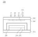
도 1은 실시예들이 적용되는 유기발광 표시장치의 시스템 구성도이다.1 is a system configuration diagram of an organic light emitting display device to which embodiments are applied.
도 1을 참조하면, 유기발광 표시장치(100)는 타이밍 제어부(110), 데이터 구동부(120), 게이트 구동부(130) 및 표시패널(140)을 포함할 수 있다.Referring to FIG. 1 , an organic light
도 1을 참조하면, 제 1 기판(110)에는 일방향으로 형성되는 다수의 데이터 라인(DL: Data Line, DL1~DLn)과 다수의 데이터 라인과 교차하는 타방향으로 형성되는 다수의 게이트 라인(GL: Gate Line, GL1~GLm)의 교차 영역마다 화소(P: Pixel)가 정의된다.Referring to FIG. 1 , the
표시패널(140) 상의 각 화소는 제 1 전극인 양극(anode), 제 2 전극인 음극(cathode) 및 유기발광층을 포함하는 적어도 하나의 유기발광소자일 수 있다. 각 유기발광소자에 포함된 유기발광층은 적색, 녹색, 청색 및 백색용 유기발광층 중 적어도 하나 이상의 유기발광층 또는 백색 유기발광층을 포함할 수 있다.Each pixel on the
각 화소에는 게이트 라인(GLy), 데이터 라인(DLx) 및 고전위전압을 공급하기 위한 고전위전압라인(VDDx)이 배치되어 있다. 또한, 각 화소에는 게이트 라인(GLy) 및 데이터 라인(DLx) 사이에서 스위칭 트랜지스터(Switching transistor)가 배치되어 있고, 양극, 음극 및 유기발광층으로 구성된 유기발광다이오드(OLED)와 스위칭 트랜지스터의 소스 전극(혹은 드레인 전극) 및 고전위전압라인(VDDx) 사이에서 구동 트랜지스터(driving transistor)가 배치되어 있다.A gate line GLy, a data line DLx, and a high potential voltage line VDDx for supplying a high potential voltage are disposed in each pixel. In addition, in each pixel, a switching transistor is disposed between the gate line GLy and the data line DLx, and an organic light emitting diode (OLED) composed of an anode, a cathode, and an organic light emitting layer and a source electrode of the switching transistor ( Alternatively, a driving transistor is disposed between the drain electrode) and the high potential voltage line (VDDx).
스위칭 트랜지스터와 구동 트랜지스터는 산화물 박막 트랜지스터(Oxide Thin Film Transistor)로서, 반도체층으로 IGZO(Indium Gallium Zinc Oxide), ZTO(Zinc Tin Oxide), ZIO(Zinc Indium Oxide) 등으로 이루어진 산화물층과 게이트 전극, 소스/드레인 전극 등을 포함할 수 있다.The switching transistor and the driving transistor are oxide thin film transistors. An oxide layer made of IGZO (Indium Gallium Zinc Oxide), ZTO (Zinc Tin Oxide), ZIO (Zinc Indium Oxide), etc. as a semiconductor layer and a gate electrode, It may include source/drain electrodes and the like.
유기발광다이오드 상에는 유기발광다이오드를 1차적으로 수분과 산소로부터 보호하는 패시베이션층이 형성될 수 있다. 한편, 패시베이션층 상에는 접착층이 형성될 수 있다. 접착층 상에 형성되는 제 2 기판이 형성될 수 있다. 접착층과 제 2 기판 사이에는 컬러필터층이 포함되어 있다.A passivation layer may be formed on the organic light emitting diode to primarily protect the organic light emitting diode from moisture and oxygen. Meanwhile, an adhesive layer may be formed on the passivation layer. A second substrate formed on the adhesive layer may be formed. A color filter layer is included between the adhesive layer and the second substrate.
이하에서는, 전술한 유기발광 표시장치에 화소를 구성하는 유기발광소자에 대하여 도면들을 참조하여 더욱 상세하게 설명한다.Hereinafter, an organic light emitting element constituting a pixel in the above-described organic light emitting display device will be described in more detail with reference to drawings.
도 2는 일 실시예에 따른 유기발광소자의 개략적인 단면도이다.2 is a schematic cross-sectional view of an organic light emitting device according to an exemplary embodiment.
도 2를 참조하면, 일 실시예에 따른 유기발광소자(200)는 화소 영역이 정의된 제 1 기판(210) 상에 위치하는 산화물 박막 트랜지스터(Oxide Thin Film Transistor, 220), 산화물 박막 트랜지스터(220) 상에 배치된 유기발광다이오드(230), 유기발광다이오드(230) 상에 배치된 패시베이션층(passivation layer, 240)을 포함할 수 있다. 또한 일 실시예에 따른 유기발광소자(200)는 패시베이션층(240) 상에 배치된 접착층(250) 및 접착층(250) 상에 배치된 컬러필터층(270), 컬러필터층(270) 상에 위치하는 제 2 기판(260)을 포함한다.Referring to FIG. 2 , the organic
일 실시예에 따른 유기발광소자(200)는 산화물 박막 트랜지스터(210)을 기준으로 발광방향이 제 2 기판(260)으로, 유기발광다이오드(230)에서 발광하는 빛이 컬러필터층(270)을 통해 외부로 방출되는 상부발광(top emission) 유기발광소자이다. 상부발광 유기발광소자는 트랜지스터들이 구성된 제1기판과 반대방향으로 발광하므로 개구율이 높고 회로 설계의 자유도가 높은 장점을 가지고 있다.In the organic
상부발광 방식으로 패시베이션층(240), 접착층(250) 및 제 2 기판(260)은 유기발광다이오드(230)에서 발광한 빛이 제 2 기판(260)으로 투과하는 재료, 예를 들어 투명한 재료(반투명한 재료 포함)로 이루어질 수 있다. 본 명세서에서 투명하다는 것은 유기발광다이오드(230)에서 발광한 빛이 외부로 투과하는 것을 의미한다.In the top emission method, the
산화물 박막 트랜지스터(220)는 폴리실리콘 트랜지스터에 비해 높은 구동 전압이 요구되지만, 공정의 수가 작아서 생산 단가가 낮은 장점을 갖는다. 또한 오프 커런트(off current) 특성이 우수하여 60Hz 이하의 저 주파수로도 구동이 가능하다.The oxide
이하 실시예들의 산화물 박막 트랜지스터(220)는 게이트전극이 소스/드레인 전극의 하부에 형성되는 바텀게이트(bottom gate) 방식을 예로써 도시하였다. 다만, 본 발명은 이에 한정되지 않고, 게이트전극이 상부에 형성되는 탑게이트(top gate) 방식일 수 있다.The oxide
이러한 산화물 박막 트랜지스터(220) 상에는 유기발광다이오드(230)가 형성된다. 유기발광다이오드(230)는 두 개의 전극들과 이들 사이에 위치하는 유기층을 포함한다. 이때 유기층은 유기발광층을 포함한다. 또한, 유기층은 원활한 엑시톤(exciton) 형성을 위해, 정공주입층, 정공수송층, 전자수송층, 전자주입층 등을 더 포함할 수 있다.An organic
다음으로, 유기발광다이오드(230) 상에는 패시베이션층(240)이 형성되는데, 필름 타입인 패시베이션층(240)은, 형성 과정에서 발생한 수소를 함유하는 수소함유 무기막으로 이루어질 수 있다.Next, a
패시베이션층(240) 상에는 접착층(250)이 형성되고, 접착층(250) 상에는 제 2 기판(260)이 형성된 하이브리드 봉지구조일 수 있다. 접착층(250)과 제 2 기판(260) 사이에는 컬러필터층(270)이 포함되어 있다.The
전술한 산화물 박막 트랜지스터(220)는 산화물(oxide)을 포함하므로, 산화물의 변화에 따른 문턱전압 시프트가 발생할 수 있다. 따라서 유기발광소자(200) 내부의 잔류 수소에 의한, 문턱전압 시프트를 방지하기 위해,Since the aforementioned oxide
유기발광다이오드(230)에 포함된 두개의 전극들 중 중 하나가 수소와 결합하거나 수소를 격자 내부에 구속하는 금속 또는 금속합금으로 이루어진 수소확산방지층을 포함할 수 있다. 또한 수소확산방지층은 유기발광소자(200)의 형성 과정에서 발생된 잔류 수소의 확산을 방지하기 위해 잔류 수소를 흡수하는 격자 틈새를 가진 면심입방 격자구조 또는 체심입방 격자구조일 수 있다.One of the two electrodes included in the organic
이하에서 유기발광소자(200)의 형성 과정에서 발생된 잔류 수소의 확산을 방지하는 수소확산방지층을 포함하는 유기발광소자 및 그 제조방법의 실시예들을 도 3 내지 도 8d를 참조하여 설명한다.Hereinafter, embodiments of an organic light emitting device including a hydrogen diffusion prevention layer for preventing diffusion of residual hydrogen generated in the process of forming the organic
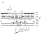
도 3은 다른 실시예에 따른 유기발광소자의 단면도이다.3 is a cross-sectional view of an organic light emitting device according to another embodiment.
도 3을 참조하면, 다른 실시예에 따른 유기발광소자(300)는 화소 영역이 정의된 제 1 기판(310) 상에 위치하는 산화물 박막 트랜지스터(Oxide Thin Film Transistor, 320), 산화물 박막 트랜지스터(320) 상에 배치된 유기발광다이오드(330), 유기발광다이오드(330) 상에 배치된 패시베이션층(passivation layer, 340)을 포함할 수 있다. 다른 실시예에 따른 유기발광소자(300)는 패시베이션층(340) 상에 형성된 접착층(350) 및 접착층(350) 상에 배치된 컬러필터층(370), 컬러필터층(370) 상에 위치하는 제 2 기판(360)을 포함한다.Referring to FIG. 3 , an organic
제 1 기판(310) 상에 산화물 박막 트랜지스터(320)가 형성된다. 산화물 박막 트랜지스터(320)는 게이트 전극(321), 게이트 전극(321) 상에 위치하고 제 1 기판(310)을 덮도록 형성되는 게이트 절연막(323), 게이트 절연막(323) 상에 위치하고 산화물로 형성된 액티브층(active layer, 325), 액티브층(325) 상에 형성되고, 제 1 전극(331)에 연결되는 소스/드레인 전극(327), 액티브층(325) 상에 위치하고 소스 전극과 드레인 전극(327) 사이에 형성되는 에치 스토퍼(etch stopper, 326)를 포함한다.An oxide
제 1 기판(310)은 글래스(Glass) 기판뿐만 아니라, PET(Polyethylen terephthalate), PEN(Polyethylen naphthalate), 폴리이미드(Polyimide) 등을 포함하는 플라스틱 기판 등일 수 있다. 또한, 제 1 기판(310) 상에는 불순원소의 침투를 차단하기 위한 버퍼층(buffering layer)이 더 구비될 수 있다. 버퍼층은 예를 들어 질화실리콘 또는 산화실리콘의 단일층 또는 다수층으로 형성될 수 있다.The
제 1 기판(310) 상에 형성되는 게이트전극(321)은 Al, Pt, Pd, Ag, Mg, Au, Ni, Nd, Ir, Cr, Li, Ca, Mo, Ti, W, Cu 중 적어도 하나 이상의 금속 또는 합금으로, 단일층 또는 다수층으로 형성될 수 있다.The
한편, 게이트 전극(321)이 형성된 제 1 기판(310) 상에 게이트 절연막(323)이 형성되어 있다. 게이트 절연막(323)은 SiOx, SiNx, SiON, Al2O3, TiO2, Ta2O5, HfO2, ZrO2, BST, PZT와 같은 무기절연물질 또는 예를 들어 벤조사이클로부텐(BCB)과 아크릴(acryl)계 수지(resin)를 포함하는 유기절연물질, 또는 이들의 조합으로 이루어질 수 있다.Meanwhile, a
게이트 절연막(323) 상에는, 산화물로 이루어진 반도체층 또는 액티브층(active layer, 325)이 배치된다. 액티브층(325)은 산화물, 예를 들어 IGZO(Indium Galium Zinc Oxide), ZTO(Zinc Tin Oxide), ZIO(Zinc Indium Oxide) 중 어느 하나의 징크옥사이드계 산화물일 수 있으나 이에 제한되지 않는다.On the
액티브층(325) 상에 위치하고, 제 1 전극(331)에 전기적으로 연결되는 소스/드레인 전극(327)은 예를 들어 Al, Pt, Pd, Ag, Mg, Au, Ni, Nd, Ir, Cr, Li, Ca, Mo, Ti, W, Cu 중 어느 하나의 금속 또는 이들의 합금으로, 단일층 또는 다수층으로 형성될 수 있다. 특히 소스/드레인전극(327)은 크롬(Cr) 또는 탄탈륨(Ta) 등과 같은 고융점 금속으로 형성될 수 있으나 이에 제한되지 않는다.The source/
액티브층(325) 상에는, 소스/드레인 전극(327) 사이에 위치하는 에치 스토퍼(326)이 형성되는데, 이는 산화물 박막 트랜지스터(320)의 포토리쏘그래피에 의한 패터닝 공정을 수행할 때, 액티브층(325)이 에칭 용액에 의해 식각되는 것을 방지한다. 다만 에치 스토퍼(326)은 에칭 용액에 따라 생략될 수 있다.On the
한편, 소스/드레인 전극(327) 상에는 소스/드레인 전극(327)과 게이트 절연막(323)을 덮도록 평탄화층(329)이 형성된다. 평탄화층(329)은 기계적 강도, 내투습성, 성막 용이성, 생산성 등을 고려하여, 소수성의 성질을 갖고, 수소함유 무기막으로서, 예를 들어 SiON, 질화실리콘(SiNx), 산화실리콘(SiOx), 산화알루미늄(AlOx) 중 어느 하나로 형성될 수 있다.Meanwhile, a
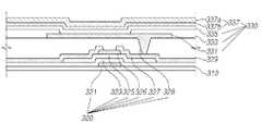
이러한 평탄화층(329) 상에는 유기발광다이오드(330)가 형성되는데, 유기발광다이오드(330)는 제 1 전극(331), 뱅크(333), 유기층(335), 제 2 전극(337)을 포함할 수 있다.An organic
제 1 전극(331)은, 평탄화층(329)에 형성된 비아 홀(328)을 통해 소스/드레인 전극(327)과 전기적으로 접촉된다.The
제 1 전극(331)은 반사효율이 우수한 금속물질, 예를 들면 알루미늄(Al) 또는 은(Ag)으로 이루어질 수 있다.The
제 1 전극(331)은, 애노드 전극(양극)으로 투명한 도전성 물질로 이루어지고 상/하부에 반사효율이 우수한 금속을 보조전극으로 포함할 수도 있다. 투명한 도전성 물질은 예를 들면 ITO 또는 IZO와 같은 금속 산화물, ZnO:Al 또는 SnO2:Sb와 같은 금속과 산화물의 혼합물, 폴리(3-메틸티오펜), 폴리[3,4-(에틸렌-1,2-디옥시)티오펜](PEDT), 폴리피롤 및 폴리아닐린과 같은 전도성 고분자 등일 수 있으나 이에 제한되지 않는다. 또한, 제 1 전극(331)은 탄소나노튜브, 그래핀, 은나노와이어 등일 수도 있다.The
한편, 제 1 전극(331)의 엣지부 상에는 뱅크(333)가 형성되고, 뱅크(333)에는 제 1 전극(331)이 노출되도록 개구부가 구비된다. 이러한 뱅크(333)는 질화실리콘(SiNx), 산화실리콘(SiOx)과 같은 무기절연물질 또는 벤조사이클로부텐(benzocyclobutene)이나 아크릴 수지(acrylic resin)와 같은 유기절연물질, 이들의 조합으로 이루어질 수 있으나 이에 제한되지 않는다.Meanwhile, a
노출된 제 1 전극(331) 상에는 유기층(335)이 형성되는데, 이러한 유기층(335)에는, 정공과 전자가 원활히 수송되어 엑시톤(exciton)을 형성할 수 있도록, 정공주입층(Hole Injection Layer, HIL), 정공수송층(Hole Transfer Layer, HTL), 유기발광층(Emitting Layer, EL), 전자수송층(Electron Transfer Layer, ETL), 전자주입층(Electron Injection Layer, EIL) 등이 차례로 적층되어 포함될 수 있다.An
유기층(335) 상에는 캐소드 전극(음극)인 제 2 전극(337)이 배치된다. 제 2 전극(337)은 유기발광층(335) 상에 순차적으로 위치하는 수소확산방지층(337b) 및 전극층(337a)을 포함할 수 있다. 이때 전술한 바와 같이 수소확산방지층(337b)은 수소와 결합하거나 수소를 격자 내부에 구속하는 금속 또는 금속합금으로 이루어질 수 있다.A
수소확산방지층(337b)은, Li, Na, Cr, α-Fe, Mo, W, K 등의 체심입방 격자구조(body-centered cubic lattice) 또는 Pt, Pb, Ni, γ-Fe, Cu, Al, Au, Ag 등의 면심입방 격자구조(face-centered cubic lattice)의 금속 또는 금속합금으로 이루어져, 금속들의 격자 사이로 잔류 수소가 확산하거나 흡수되기 때문에, 잔류 수소가 산화물 박막 트랜지스터(320) 방향으로 확산되는 것을 방지할 수 있다.The hydrogen
체심입방 격자구조를 가지는 금속 또는 금속 합금은 32%의 공극을 가지고 면심입방 격자구조를 가지는 금속 또는 금속 합금은 26%의 공극을 가지므로 패시베이션층(340)이나 평탄화층(329)가 증착되는 과정에서 생겨난 잔류 수소가 수소확산방지층(337b) 내로 확산되어 수소확산방지층(337b)의 내부에 고착되므로, 산화물 박막 트랜지스터(320)의 액티브층(325)으로 더 이상 확산되는 것을 방지할 수 있다.Since the metal or metal alloy having a body-centered cubic lattice structure has voids of 32% and the metal or metal alloy having a face-centered cubic lattice structure has 26% voids, the
전극층(337a)는 캐소드 전극(음극)으로 유기층(335)에서 발광한 빛이 제 2 기판(360)으로 방출하도록 투명한 도전성 물질로 이루어질 수 있다. 투명한 도전성 물질은 예를 들면 ITO(Indium Tin Oxide) 또는 IZO(Indium Zinc Oxide), IGZO(Indium Galium Zinc Oxide)와 같은 금속 산화물, ZnO:Al 또는 SnO2:Sb와 같은 금속과 산화물의 혼합물, 폴리(3-메틸티오펜), 폴리[3,4-(에틸렌-1,2-디옥시)티오펜](PEDT), 폴리피롤 및 폴리아닐린과 같은 전도성 고분자 등일 수 있으나 이에 제한되지 않는다. 또한, 제 2 전극(336)은 탄소나노튜브, 그래핀, 은나노와이어 등일 수도 있다. 특히 전극층(337a)은 전술한 금속 산화물로 이루어질 수 있다.The
예를 들어 수소확산방지층(337b)는 금속합금인 ZnNi로 이루어지고, 전극층(337a)는 금속산화물인 ITO(Indium Tin Oxide)로 이루어질 수 있다.For example, the hydrogen
제2전극(337)에 포함되는 수소확산방지층(337b)과 전극층(337a)는 각각 단일층 또는 다층일 수 있다. 한편, 수소확산방지층(337b)과 전극층(337a)은 화소 영역 전체에 배치되어 잔류 수소가 산화물 박막 트랜지스터(325)로 확산되는 것을 전면적으로 방지할 수 있다.The hydrogen
유기발광다이오드(330) 상에는 제 2 전극(337)의 상면 전체를 덮도록 패시베이션층(passivation layer, 340)이 형성된다.A
패시베이션층(340)은 기계적 강도, 내투습성, 성막 용이성, 생산성 등을 고려하여, 소수성의 성질을 갖고, 수소함유 무기막으로서, SiON, 질화실리콘(SiNx), 산화실리콘(SiOx), 산화알루미늄(AlOx) 중 어느 하나로 형성될 수 있다.The
필름 타입의 패시베이션층(340)은 수분이나 산소의 침투를 더디게 함으로써, 수분과 산소에 민감한 유기층(335)이 수분과 접촉되는 것이 방지될 수 있다.The film-
이러한 패시베이션층(340)은 보호층으로서 기능하는 것 이외에도, Ba, Ca, Cu, Fe, Hf, La, Mg, Nb, Ni, Pd, Pt, Se, Sr, Ta, Ti, V, Zr 중 적어도 하나의 금속을 포함하는 비드(bid)를 더 포함함으로써, 후술할 소자 내부의 잔류 수소가 산화물 박막 트랜지스터(320)로 확산되는 것을 막는 역할을 할 수도 있다.In addition to functioning as a protective layer, the
패시베이션층(240)은 0.5μm 에서 1.0μm 의 상대적으로 두꺼운 두께를 갖도록 단일층으로 형성되나, 이에 한정되지 않고 다수층으로 형성될 수 있다.The
평탄화층(329) 또는 패시베이션층(340)은 화학기상증착, 물리기상증착, 플라즈마 화학기상증착 등의 공정으로 형성될 수 있다. 특히 플라즈마 화학기상증착으로 평탄화층(329) 또는 패시베이션층(340)을 형성할 경우 유기발광소자(300) 내부를 빠져나가지 못하는 잔류 수소가 발생된다. 패널 내부의 잔류 수소가 발생시키는 문제점에 대한 상세한 설명은 후술한다.The
한편, 패시베이션층(340) 상에는 접착층(350)이 형성되는데, 접착층(350)은 광 투과율이 우수한 투명성 접착 재료, 예를 들어 접착 필름(adhesive film) 또는 OCA(Optical Cleared Adhesive)로 형성될 수 있다. 접착층의 형성 방식은 금속리드(metal lid), 프릿실링(frit sealing), 박막(thin film) 증착 방식에 의할 수 있다.Meanwhile, an
접착층(350)은 제 2 기판(360)의 전면에 접착되는 전면봉지(face sealing)구조로 이루어질 수 있으나, 이에 한정되지 않는다. 이러한 접착층(350)은 습기와 같은 외부 요인으로부터 유기발광다이오드(330)를 보호함과 아울러, 유기발광다이오드(330)를 봉지하는 제 2 기판(360)을 평탄화시킨다.The
또한, 접착층(350)은, 예를 들어 Ba, Ca, Cu, Fe, Hf, La, Mg, Nb, Ni, Pd, Pt, Se, Sr, Ta, Ti, V, Zr 중 적어도 하나를 비드(bid)로 포함함으로써, 소자 내부의 잔류 수소를 흡수하는 역할을 할 수도 있다.In addition, the
한편, 접착층(350) 상에는 컬러필터층(370)과 제 2 기판(360)이 배치된다.Meanwhile, the
컬러필터층(370)은 컬러필터(372)와 컬러필터(372) 주위에 배치된 블랙매트릭스(374)를 포함할 수 있다.The
제 2 기판(360)은 글래스(Glass) 기판뿐만 아니라, PET(Polyethylen terephthalate), PEN(Polyethylen naphthalate), 폴리이미드(Polyimide) 등을 포함하는 플라스틱 기판 등일 수 있다.The
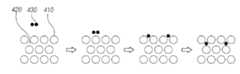
도 4는 소자 공정 중 발생한 잔류 수소가 수소확산방지층 내부로 흡수되는 메커니즘을 상세하게 설명한다.4 explains in detail the mechanism by which residual hydrogen generated during the device process is absorbed into the hydrogen diffusion barrier layer.
도 4를 참조하면, 산화물 박막 트랜지스터(320)의 액티브층(325) 산화물을 환원시켜 소자 특성에 변화를 주는 것은 잔류 수소(430)이다.Referring to FIG. 4 , it is the
즉, 가스는 플라즈마 상태가 되면 다양한 형태로 분해되어 소자 내에 잔류하게 될 수 있다. 예를 들어, 플라즈마 화학기상증착(Plasma Enhanced Chemical Vapor Deposition, PECVD)과 같이 수소화실리콘(SiH4)과 아민(NH3) 가스의 플라즈마를 이용하는 증착 공정 중에, 상온처럼 저온에서도 단원자 또는 이온상태로 고체 내부를 쉽게 이동할 수 있는 확산성 수소(Diffusible Hydrogen)와 다른 원자와 결합하여 분자상으로 변한 비확산성 수소가 발생된다.That is, when the gas is in a plasma state, it may be decomposed into various forms and remain in the device. For example, during a deposition process using plasma of silicon hydride (SiH4) and amine (NH3) gas, such as plasma enhanced chemical vapor deposition (PECVD), the inside of a solid in a monoatomic or ionic state even at a low temperature like room temperature Diffusible Hydrogen, which can move easily, and non-diffusible Hydrogen, which is changed into a molecular phase by combining with other atoms, are generated.
일반적인 유기발광소자(300)의 경우 잔류 수소가 발생하면, 고체 내부를 자유롭게 이동하게 된다. 특히 제1기판(310)과 제2기판(360)이 통상의 글래스 기판을 사용하는 경우에는, 잔류 수소(430)가 양 글래스 기판들(310, 360) 사이에 갇히게 됨으로써, 이 중 일부가 산화물 박막 트랜지스터(320)의 액티브층(325)에 도달할 수 있다.In the case of a general organic
특히 평탄화층(329)이나 패시베이션층(340)으로 성막되는 질화실리콘(SiNx), SiON 등이 플라즈마 화학기상증착(Plasma Enhanced Chemical Vapor Deposition, PECVD)되는 경우, 많은 양의 수소 및 불순물들이 발생한다. 특히 유기발광소자(300)의 경우 유기층(335)의 열적 손상 문제로 인하여 공정 온도가 100℃ 이내로 제한되기 때문에, 잔류 수소(430)의 양이 늘어날 수밖에 없다.In particular, when silicon nitride (SiNx), SiON, or the like formed as the
화학식 1을 참조하여 설명하면, SiH4 와 NH3의 혼합 가스를 이용하여 플라즈마화학기상증착 공정으로 질화실리콘을 증착하여 패시베이션층(340)을 형성하면, 패시베이션층(340) 또는 다른 층 중에 약 15 ~ 40% 가량의 잔류 수소(H2, 430)가 발생된다.Referring to Formula 1, when the
[화학식 1] [Formula 1]
SiH4 + 2NH3 → SiN2 + 5H2SiH4 + 2NH3 → SiN2 + 5H2
잔류 수소(430)는 도 3에 도시한 다른 실시예에 따른 유기발광소자(300)의 수소확산방지층(337a)를 이루는 재료(410), 예를 들어 금속 또는 금속 합금와 결합하거나, 금속 또는 금속합금의 격자 구조의 공극(420)에 구속될 수 있다.The
도 5a는 수소확산방지층을 포함하지 않는 유기발광소자 내부의 잔류 수소가 산화물 박막 트랜지스터로 확산되어 산화물 박막 트랜지스터의 문턱 전압을 시프트시키는 단면도이고, 도 5b는 도 3의 다른 실시예에 따른 유기발광소자 내부의 잔류 수소가 수소확산방지층의 내부에 흡수되어 산화물 박막 트랜지스터로 확산되지 않는 것을 나타내는 단면도이다.5A is a cross-sectional view of shifting the threshold voltage of the oxide thin film transistor by diffusing residual hydrogen inside the organic light emitting device not including the hydrogen diffusion prevention layer into the oxide thin film transistor, and FIG. 5b is an organic light emitting device according to another embodiment of FIG. 3 It is a cross-sectional view showing that residual hydrogen inside is absorbed into the hydrogen diffusion prevention layer and is not diffused into the oxide thin film transistor.
도 5a를 참조하면, 제 2 기판(360)이 글래스 기판인 경우이고, 증착 공정에서 발생된 잔류 수소(630)는, 수소 분자 상태인 비확산성 수소(510)와 원자 상태로 해리된 확산성 수소(520)로 이루어진다. 패시베이션층(340)과 접착층(350)의 증착 공정에서 발생되어 소자 내부에 잔류된 확산성 수소(520)는 제 1 기판(310) 또는 제 2 기판(360)(특히 제 2 기판)에서 흡수하지 못하므로, 제 1 기판(310)과 제 2 기판(360) 사이에서 자유롭게 확산될 수 있다. 따라서 확산성 수소(520)의 일부가 산화물 박막 트랜지스터(320)로 확산되어, 산화물 박막 트랜지스터(320)의 액티브층(325)를 구성하는 산화물을 환원시킬 수 있다.Referring to FIG. 5A , when the
이러한 액티브층(325)의 환원은 결국 산화물 박막 트랜지스터(320)의 전기적 거동의 변화를 일으켜 문턱전압 시프트(threshold voltage shift)를 야기한다. 다시 말해 확산성 수소(520)는 산화물 반도체로 구성된 액티브층(325)에 도펀트로 작용하여 산화물 박막 트랜지스터(320)의 문턱전압을 음의 방향으로 이동시킨다. 문턱전압 시프트의 정도가 표시패널의 회로 보상 범위를 벗어나게 된다면, 화면에 영향을 주어 얼룩을 발생시키거나, 휘도 편차가 발생될 수 있다.The reduction of the
도 5b를 참조하면, 패시베이션층(340)과 산화물 박막 트랜지스터(320), 구체적으로 유기층(335)와 전극층(337a)사이에 수소확산방지층(337b)를 포함하는 다른 실시예에 따른 유기발광소자(300)는 평탄화층(329)이나 패시베이션층(340) 등의 적층 구조에 존재하는 확산성 수소(520)가 수소확산방지층(337b)의 내부에 흡수되어 산화물 박막 트랜지스터(320)로 확산되지 않도록 하므로, 산화물 박막 트랜지스터(320)의 환원이 방지될 수 있다.Referring to FIG. 5B, an organic light emitting device according to another embodiment including a hydrogen
도 3 및 도 5b의 다른 실시예에 따른 유기발광소자(300)는 이물로 인한 전극들 사이의 쇼트를 방지하는 이물 보상층의 기능을 하는 수소확산방지층(337b)을 표시패널 내에 포함시키는 구조를 제안한다.The organic
도 6은 도 5a의 유기발광소자와, 도 3 및 도 5b의 다른 실시예에 따른 유기발광소자의 이물 보상 기능을 비교한 도면이다.FIG. 6 is a view comparing foreign material compensation functions of the organic light emitting diode of FIG. 5A and the organic light emitting diode according to other exemplary embodiments of FIGS. 3 and 5B .
도 6에서 610은 패널공정 과정에서 침투한 이물을 지시한다. 도 5a의 유기발광소자(500)에서 수소확산방지층(337b)을 포함하지 않는 전극층(337a)은 이물(610)이 침투할 경우 제1전극(331)과 쇼트가 발생한다. 다시 말해 제2전극인 전극층(337a)은 산화물 계열의 투명전도막을 사용하기 때문에 산화물 계열의 투명전도막을 산화시켜 제1전극(331)과 쇼트를 방지하는 기술을 적용할 수 없다.In FIG. 6, 610 indicates a foreign material that has penetrated during the panel process. In the organic
반면 도 3 및 도 5b의 다른 실시예에 따른 유기발광소자(300)에서, 수소확산방지층(337b)과 전극층(337a)을 포함하는 제2전극(337)은 수소확산방지층(337b)으로 인하여 이물(610)이 침투하여도 제1전극(210)과 전극층(337a) 사이에 쇼트가 발생하지 않아 암점 등과 같은 불량이 발생하지 않는다. 다시 말해 금속 또는 금속합금으로 이루어진 수소확산방지층(337b)을 산화시켜 제1전극(331)과 쇼트를 방지하는 기술을 적용할 수 있다. 즉 IZO, ITO, IGZO와 같은 TCO(transparent conductive oxide)를 전극층(337a)으로 증착하기 전에 산화에 의한 쇼트 방지기술이 적용된 수소확산방지층(337b)을 형성하므로 제1전극(331)과 쇼트를 방지할 수 있다. 이때 수소확산방지층(337b)의 표면이 산화되어 있다. 아울러, 도 6에 도시한 바와 같이 수소확산방지층(337b)과 제1전극(331)의 계면이 산화되어 있다. 이때 수소확산방지층(337b)과 제1전극(331)의 계면의 산화가 이물에 의한 쇼트를 오픈시키는 주된 역할을 한다.On the other hand, in the organic
도 3 및 도 5b의 다른 실시예에 따른 유기발광소자(300)를 적용할 경우, 제2전극(337)에 별도의 공정 없이 이물 보상층 기능을 하는 수소확산방지층(337)을 형성하므로, 제1전극(예를 들어 애노드)와 제2전극(예를 들어 캐소드)의 쇼트를 방지하여 암점 불량 발생 가능성을 낮추며, 패널 수율을 증가시킨다.When the organic
도 7a는 도 5a의 유기발광소자에서 전극층의 투과도를 나타내고 있다. 도 7b는 도 3 및 도 5b의 다른 실시예에 따른 유기발광소자에서 제2전극의 투과도를 나타내고 있다.FIG. 7a shows the transmittance of the electrode layer in the organic light emitting device of FIG. 5a. FIG. 7B shows the transmittance of the second electrode in the organic light emitting device according to another embodiment of FIGS. 3 and 5B.
도 7a를 참조하면, 도 5a의 유기발광소자(500)의 투명전극인 전극층(337a)은 가시광선 영역에서 평균 90% 이상의 투과도를 나타내지만 특정 파장(Blue영역)에서는 투과도가 90% 미만으로 저하되는 특성을 나타낸다.Referring to FIG. 7A, the
도 7b를 참조하면, 도 3 및 도 5b의 다른 실시예에 따른 유기발광소자(300)는 투명전극으로 수소확산방지층(337b)와 전극층(337a)을 포함하므로 가시광선 전체 영역에서 평균 90%이상의 투과도를 나타내며, 특정파장(블루 영역, 예를 들어 400nm~450nm의 가시광선 영역)에서도 투과도가 평균 90% 이상인 투과도를 나타낸다.Referring to FIG. 7B , since the organic
특히 도 3 및 도 5b의 다른 실시예에 따른 유기발광소자(300)에서 수소확산방지층(337b)의 두께(도 3에 도시한 t1)는 전극층(337a)의 두께(도 3에 도시한 t2)보다 작다. 즉 수소확산방지층(337b)은 전극층(337a)보다 두께가 얇을 수 있다(t2>T1). 예를 들어 수소확산방지층의 두께는 10 ~ 1000Å일 수 있다. 두께가 얇은 금속계열의 수소확산층(337b)과 두께가 두꺼운 금속산화물계열의 전극층(337a)을 2중으로 포함하는 구조로 제2전극(337)을 구성하므로 전체 가시광선 영역의 평균 투과도(90%이상) 및 블루 영역(예를 들어 400nm~450nm의 가시광선 영역)의 투과도(90%이상)를 증가시킬 수 있다.In particular, in the organic
따라서, 도 3 및 도 5b의 다른 실시예에 따른 유기발광소자(300)를 적용 시 전체 가시광선 영역의 평균 투과도(90%이상) 및 블루 영역(예를 들어 400nm~450nm의 가시광선 영역)의 투과도(90%이상)를 증가시킴으로써, 패널 효율을 증가시킬 수 있다.Therefore, when the organic
이상에서 다른 실시예에 따른 유기발광소자(300)를 설명하였고, 이하에서 또다른 실시예들에 따른 유기발광소자의 제조 공정에 대해 설명한다.The organic
도 8a 내지 도 8d는 또다른 실시예에 따른 유기발광소자의 일 제조공정 단면도들이다.8A to 8D are cross-sectional views of a manufacturing process of an organic light emitting device according to another embodiment.
우선 도 8a를 참조하면, 제 1 기판(310)이 준비되고, 제 1 기판(310)의 세정 단계를 거친 후, 산화물 박막 트랜지스터(320)가 형성된다. 제 1 기판(310) 세정 단계에서는 표면 개선을 위해 플라즈마 처리(plasma treatment)가 수반될 수 있다.First, referring to FIG. 8A , a
제 1 기판(310)은 소자를 형성하기 위한 재료로 기계적 강도나 치수 안정성이 우수한 것을 선택할 수 있다. 일실시예에 따른 유기발광소자(300)는 제 1 기판(310)은 글래스(Glass) 기판뿐만 아니라, PET(Polyethylen terephthalate), PEN(Polyethylen naphthalate), 폴리이미드(Polyimide) 등을 포함하는 플라스틱 기판 등일 수 있다.For the
한편, 제 1 기판(310) 상에는 불순원소의 침투를 차단하기 위한 버퍼층(buffering layer)이 더 형성될 수 있다. 버퍼층은 예를 들어 질화실리콘 또는 산화실리콘의 단일층 또는 다수층으로 형성될 수 있다.Meanwhile, a buffering layer may be further formed on the
이러한 제 1 기판(310) 상에는 산화물 박막 트랜지스터(320)가 형성된다.An oxide
산화물 박막 트랜지스터(320)는 절연물질로 이루어진 제 1 기판(310) 상에 알루미늄, 구리 등과 같이 전기적 저항이 작고 인장 응력(tensil stress)을 가지는 도전성 금속으로 이루어진 게이트 전극(321)이 형성된다.In the oxide
게이트 전극(321)은 Al, Pt, Pd, Ag, Mg, Au, Ni, Nd, Ir, Cr, Li, Ca, Mo, Ti, W, Cu 중 적어도 하나 이상의 금속 또는 합금으로, 단일층 또는 다수층으로 형성될 수 있다.The
또한, 제 1 기판(310) 상에 SiOx, SiNx, SiON, Al2O3, TiO2, Ta2O5, HfO2, ZrO2, BST, PZT와 같은 무기절연물질 또는 벤조사이클로부텐(BCB)과 아크릴(acryl)계 수지(resin)를 포함하는 유기절연물질, 또는 이들의 조합으로 이루어진 게이트 절연막(323)이 형성된다. 게이트 절연막(323) 상에 게이트 전극(321)이 중앙에 위치하도록 IGZO, ZTO(Zinc Tin Oxide), ZIO(Zinc Indium Oxide) 등 징크옥사이드계 산화물로 이루어진 액티브층(325)이 형성된다.In addition, inorganic insulating materials such as SiOx, SiNx, SiON, Al2O3, TiO2, Ta2O5, HfO2, ZrO2, BST, PZT or benzocyclobutene (BCB) and acrylic resin are formed on the
액티브층(325) 상에 소스/드레인 전극(327)이 형성되고, 소스/드레인전극(327)은 예를 들어 Al, Pt, Pd, Ag, Mg, Au, Ni, Nd, Ir, Cr, Li, Ca, Mo, Ti, W, Cu 중 어느 하나의 금속 또는 이들의 합금으로, 단일층 또는 다수층으로 형성될 수 있다. 특히 소스/드레인전극(327)은 크롬(Cr) 또는 탄탈륨(Ta) 등과 같은 고융점 금속으로 형성될 수 있으나 이에 제한되지 않는다.A source/
이러한 산화물 박막 트랜지스터(320)의 형성 방법은, 우선 제 1 기판(310) 상에 알루미늄, 구리 등과 같은 도전성 금속을 화학기상증착(Chemical Vapor Deposition) 방법이나, 스퍼터링(sputtering) 등의 물리기상증착(Physical Vapor Deposition) 방법으로 증착한 후 포토리쏘그래피(photolithography) 방법으로 패터닝하여 게이트 전극(321)를 형성한다.The method of forming the oxide
그리고, 기판(310) 상에 게이트 전극(321)을 덮도록 산화실리콘 또는 질화실리콘을 화학기상증착 방법으로 증착하여 게이트 절연막(323)을 형성한다.Then, silicon oxide or silicon nitride is deposited on the
이후 게이트 절연막(323) 상에 불순물이 도핑되지 않은 IGZO(Indium Gallium Zinc Oxide), ZTO(Zinc Tin Oxide) 또는 ZIO(Zinc Indium Oxide) 등을 화학기상증착 등의 방법으로 순차적으로 증착하여 액티브층(325)을 형성한다.Thereafter, IGZO (Indium Gallium Zinc Oxide), ZTO (Zinc Tin Oxide), ZIO (Zinc Indium Oxide), etc., which are not doped with impurities, are sequentially deposited on the
이어서 크롬 또는 탄탈륨 등의 금속을 화학기상증착 등의 증착 방법과 포토리쏘그래피 방식으로 이중 단차를 갖도록 소스/드레인전극(327)을 형성한다.Subsequently, source/
다음 단계로서, 게이트 절연막(323) 상에 소스/드레인전극(327)과 액티브층(325)의 노출된 부분을 덮도록 수소함유 무기막, 예를 들어 산화실리콘 또는 질화실리콘을 증착하여 평탄화층(329)을 형성한다. 이 때, 소스/드레인전극(327)이 2중의 단차를 가지므로 평탄화층(329)의 스텝 커버리지(step coverage)가 저하되는 것이 방지된다.As a next step, a planarization layer ( 329) form. At this time, since the source/
이후 평탄화층(329)을 패터닝하여 드레인전극(327)을 노출시키는 비아홀(328)을 형성한다.Thereafter, the
도 8b를 참조하면, 제 1 전극, 유기층 및 제 2 전극을 포함하는 유기발광다이오드(330)을 형성한다.Referring to FIG. 8B , an organic
우선 제 1 전극(331)이 평탄화층(329) 상에 형성된다. 제 1 전극(331)은 각 화소 영역별로 형성되는데, 비아홀(328)을 통해 드레인 전극(327)과 전기적으로 접촉되고, ITO(Indium Tin Oxide)와 같은 투명 재료로 패터닝될 수 있다. 포토레지스트(photoresist)를 스핀 코팅한 후, 프리 베이킹(pre-baking), 노광, 현상, 포스트 베이킹(post-baking), 에칭(etching) 과정을 거쳐 포토레지스트를 벗겨내는, 포토리쏘그래피 과정을 통해 패터닝된다. 제 1 전극(331)은 정공(hole)을 발생시키는 양극(anode)이 될 수 있다.First, a
이후 제 1 전극(331)의 엣지부에 형성되어 제 1 전극(331)의 일부분을 노출시키는 개구부가 형성된 뱅크(333)가 형성된다. 뱅크(333)는 각종 트랜지스터 및 각종 배선들이 형성되어 표면이 매끄럽지 못하고, 울퉁불퉁하게 단차가 형성된 표면 위에 유기막을 형성할 경우, 단차진 부분에서 유기물이 열화되는 것을 방지하기 위한 것이다. 즉, 산화물 박막 트랜지스터(320) 및 각종 배선들이 형성된 영역과, 평탄한 기판 위에 단순히 박막들만 적층되어 평탄한 발광 영역을 구분하기 위해 비발광 영역 위에 뱅크(333)가 형성된다.Thereafter, a
노출된 제 1 전극(331)과 뱅크(333) 상에는 유기층(335)이 형성된다. 보다 구체적으로는 정공주입층(HIL), 정공수송층(HTL), 발광층(EL), 전자수송층(ETL), 전자주입층(HIL)이 순차적으로 적층된다. 정공과 전자가 발광층에서 만나 여기자(Exciton)을 형성하고, 여기자가 여기상태(excited state)에서 기저상태(ground state)로 떨어지면서 발광을 일으켜 화상을 표시하게 된다.An
이러한 유기층(335)을 화학기상증착, 물리기상증착, 용액 공정 등의 방법으로 형성할 수 있다. 예를 들어, 유기발광층은, 미세형상 금속마스크(Fine Metal Mask, FMM)를 이용하여 RGB 발광 물질을 증착하거나, LITI(Laser Induced Thermal Imaging) 방법 또는 스핀 코팅(spin coating)등의 용액 공정이 수행될 수 있다. LITI 방식은 레이저 빔을 도너 필름(donor film) 위에서 선택적으로 조사하여, 방출되는 열에 의해 박막이 선택적으로 전사(transfer)되는 방식이다.The
이어서, 유기층(335) 상에는 열증착 또는 이온 빔 증착을 통해, 수소확산방지층(337b)이 형성된다. 수소확산방지층(337b)은 금속 또는 금속합금일 수 있다. 이때, 수소확산방지층(337b)은 열이나 플라즈마에 의한 유기층(335)의 손상을 최소화하기 위하여 저온 증착에 의해 형성할 수 있으나 이에 제한되지 않는다.Subsequently, a hydrogen
유기층(335) 상에 수소확산방지층(337b)를 형성한 후 수소확산방지층(337b)을 산화시키므로 제1전극(331)과 제2전극(337)이 이물에 의해 쇼트되는 것을 방지할 수 있다. 이때 수소확산방지층(337b)의 표면 및 수소확산방지층(337b)과 제1전극(331)의 계면을 산화시킨다. 구체적으로 수소확산방지층(337b)을 형성한 상태에서 예를 들어 O2또는 O2를 포함하는 공정 가스의 공정조건에서 저전위 전원전압 배선(VSS)과 고전위 전원전압(VDD) 배선 등 특정 전압을 인가할 수 있다. 이때 회로적으로 위 배선들을 통해 수소확산방지층(337b)에 전류가 흐르게 되고 이 수소확산방지층(337b)에 포함되는 금속 또는 금속합금과 전술한 공정 가스와 반응하여 수소확산방지층(337b)의 표면 및 수소확산방지층(337b)과 제1전극(331)의 계면이 산화된다. 특히 전류에 의한 줄열(Joule Heating)에 의해 수소확산방지층(337b)의 표면 및 수소확산방지층(337b)과 제1전극(331)의 계면의 산화가 가속화된다. 특히 수소확산방지층(337b)과 제1전극(331)의 계면과 같이 쇼트 발생 부위는 상태적으로 계면 불안정성이 높아 컨택 저항이 높기 때문에 가열 속도(Heating rate)가 높아 산화가 더욱 가속화된다.After the hydrogen
도 8c를 참조하면, 수소확산방지층(337b) 상에 전극층(337a)을 형성한다. 전극층(337a)은 금속산화물, 전도성 고분자, 탄소나노튜브, 그래핀, 은나노와이어 중 하나로 전체 화소 영역에 형성한다.Referring to FIG. 8C , an
이어서 도 8d를 참조하면, 유기발광다이오드(330) 상에 패시베이션층(340)을 형성한다.Referring to FIG. 8D , a
패시베이션층(340)은 유기발광다이오드(330)를 수분과 불순물로부터 1차적으로 보호하는 역할을 한다. SiON, 질화실리콘(SiNx), 산화실리콘(SiOx), 산화알루미늄(AlOx)으로 화학기상증착, 물리기상증착, 플라즈마 화학기상증착 등의 공정을 통해 패시베이션층(340)을 형성한다. 이 과정에서 잔류 수소(630)가 발생하게 된다.The
패시베이션층(240)은, 증착 공정시에 발생하는 수소를 함유하는, 수소함유 무기막(예를 들어 SiON, 질화실리콘(SiNx), 산화실리콘(SiOx), 산화알루미늄(AlOx))으로서, 0.5μm 에서 1.0μm 의 상대적으로 두꺼운 두께를 갖도록 단일층으로 형성되나, 이에 한정되지 않고 다수층으로 형성될 수 있다.The
화학식 1을 참조하여 설명한 바와 같이 SiH4 와 NH3의 혼합 가스를 이용하여 플라즈마화학기상증착 공정으로 질화실리콘을 증착하여 패시베이션층(240)을 형성할 수 있다.As described with reference to Chemical Formula 1, the
패시베이션층(340)의 형성 공정과 별도로 제 2 기판(360)에 컬러필터(372)과 블랙매트릭스(374)을 포함하는 컬러필터층(370)을 형성하고, 제1기판(310)의 패시베이션층(340) 상에 접착층(350)을 이용하여 컬러필터층(370)이 형성된 제2기판(360)을 합착한다. 이를 통해 다른 실시예에 따른 유기발광소자(300)가 완성된다.Separately from the process of forming the
패시베이션층(340)과 산화물 박막 트랜지스터(320) 사이에 수소확산방지층를 포함하는 실시예들에 따른 유기발광소자(300)는 패시베이션층(340) 내부의 수소가 산화물반도체로 확산하는 것을 방지하는 기능을 포함할 뿐만 아니라, 기존의 이물에 의한 암점 발생 방지 및 패널 효율 향상의 효과도 동시에 구현할 수 있다.The organic
이상 도면을 참조하여 실시예들을 설명하였으나 본 발명은 이에 제한되지 않는다.Although embodiments have been described with reference to the drawings, the present invention is not limited thereto.
이상에서 기재된 "포함하다", "구성하다" 또는 "가지다" 등의 용어는, 특별히 반대되는 기재가 없는 한, 해당 구성 요소가 내재될 수 있음을 의미하는 것이므로, 다른 구성 요소를 제외하는 것이 아니라 다른 구성 요소를 더 포함할 수 있는 것으로 해석되어야 한다. 기술적이거나 과학적인 용어를 포함한 모든 용어들은, 다르게 정의되지 않는 한, 본 발명이 속하는 기술 분야에서 통상의 지식을 가진 자에 의해 일반적으로 이해되는 것과 동일한 의미를 가진다. 사전에 정의된 용어와 같이 일반적으로 사용되는 용어들은 관련 기술의 문맥 상의 의미와 일치하는 것으로 해석되어야 하며, 본 발명에서 명백하게 정의하지 않는 한, 이상적이거나 과도하게 형식적인 의미로 해석되지 않는다.Terms such as "comprise", "comprise" or "having" described above mean that the corresponding component may be inherent unless otherwise stated, and therefore do not exclude other components. It should be construed that it may further include other components. All terms, including technical or scientific terms, have the same meaning as commonly understood by one of ordinary skill in the art to which the present invention belongs, unless defined otherwise. Commonly used terms, such as terms defined in a dictionary, should be interpreted as consistent with the meaning in the context of the related art, and unless explicitly defined in the present invention, they are not interpreted in an ideal or excessively formal meaning.
이상의 설명은 본 발명의 기술 사상을 예시적으로 설명한 것에 불과한 것으로서, 본 발명이 속하는 기술 분야에서 통상의 지식을 가진 자라면 본 발명의 본질적인 특성에서 벗어나지 않는 범위에서 다양한 수정 및 변형이 가능할 것이다. 따라서, 본 발명에 개시된 실시예들은 본 발명의 기술 사상을 한정하기 위한 것이 아니라 설명하기 위한 것이고, 이러한 실시예에 의하여 본 발명의 기술 사상의 범위가 한정되는 것은 아니다. 본 발명의 보호 범위는 아래의 청구범위에 의하여 해석되어야 하며, 그와 동등한 범위 내에 있는 모든 기술 사상은 본 발명의 권리범위에 포함되는 것으로 해석되어야 할 것이다.The above description is merely an example of the technical idea of the present invention, and various modifications and variations can be made to those skilled in the art without departing from the essential characteristics of the present invention. Therefore, the embodiments disclosed in the present invention are not intended to limit the technical spirit of the present invention, but to explain, and the scope of the technical spirit of the present invention is not limited by these embodiments. The protection scope of the present invention should be construed according to the claims below, and all technical ideas within the equivalent range should be construed as being included in the scope of the present invention.
Claims (10)
Translated fromKorean상기 산화물 박막 트랜지스터 상에 제1전극, 제2전극, 상기 제1전극과 상기 제2전극 사이에 위치하는 유기발광층을 포함하는 유기발광다이오드; 및
상기 유기발광다이오드 상에 수소를 함유하는 수소함유 무기막으로 이루어진 패시베이션층(passivation layer)을 포함하고,
상기 제2전극은 상기 유기발광층 상에 순차적으로 위치하는 수소확산방지층 및 전극층을 포함하며, 상기 수소확산방지층은 수소와 결합하거나 수소를 격자 내부에 구속하는 금속 또는 금속합금으로 이루어지며,
상기 수소확산방지층은 상기 유기발광층과 상기 전극층 사이에 위치하며,
상기 수소확산방지층의 표면은 산화되어 있는 유기발광소자.an oxide thin film transistor positioned on a first substrate in which a pixel region is defined;
an organic light emitting diode including a first electrode, a second electrode, and an organic light emitting layer positioned between the first electrode and the second electrode on the oxide thin film transistor; and
A passivation layer made of a hydrogen-containing inorganic film containing hydrogen is included on the organic light-emitting diode,
The second electrode includes a hydrogen diffusion prevention layer and an electrode layer sequentially positioned on the organic light emitting layer, and the hydrogen diffusion prevention layer is made of a metal or metal alloy that bonds with hydrogen or confines hydrogen to the inside of the lattice,
The hydrogen diffusion prevention layer is located between the organic light emitting layer and the electrode layer,
An organic light emitting device in which the surface of the hydrogen diffusion prevention layer is oxidized.
상기 패시베이션층 상에 위치하는 접착층;
상기 접착층 상에 위치하는 제2기판; 및
상기 접착층과 상기 제2기판 사이에 위치하는 컬러필터층을 포함하는 유기발광소자.According to claim 1,
an adhesive layer positioned on the passivation layer;
a second substrate positioned on the adhesive layer; and
An organic light emitting device comprising a color filter layer positioned between the adhesive layer and the second substrate.
상기 전극층은 금속산화물, 전도성 고분자, 탄소나노튜브, 그래핀, 은나노와이어 중 하나로 이루어지고, 상기 수소확산방지층은 금속합금으로 이루어진 유기발광소자.According to claim 1,
The electrode layer is made of one of metal oxides, conductive polymers, carbon nanotubes, graphene, and silver nanowires, and the hydrogen diffusion prevention layer is made of a metal alloy.
상기 금속산화물은 ITO(Indium Tin Oxide)이며, 상기 금속합금은 ZnNi인 유기발광소자.According to claim 3,
The metal oxide is indium tin oxide (ITO), and the metal alloy is ZnNi.
상기 제2전극의 투과율이 400nm~450nm의 가시광선 영역에서 평균 90% 이상인 유기발광소자.According to claim 1,
An organic light emitting device having an average transmittance of 90% or more in the visible ray region of 400 nm to 450 nm.
상기 제2전극의 투과율이 가시광선 전체 영역에서 평균 90% 이상인 유기발광소자.According to claim 5,
An organic light emitting device having an average transmittance of 90% or more in the entire visible light region.
상기 수소확산방지층은 상기 전극층보다 두께가 얇은 유기발광소자.According to claim 5,
The hydrogen diffusion prevention layer is an organic light emitting device having a thinner thickness than the electrode layer.
상기 수소확산방지층과 상기 전극층은 상기 화소 영역 전체에 배치된 유기발광소자.According to claim 1,
The hydrogen diffusion prevention layer and the electrode layer are disposed over the entire pixel area.
상기 제 1 기판의 화소 영역에 대응되도록 상기 산화물 박막 트랜지스터 상에 유기발광다이오드를 형성하는 단계;
상기 유기발광다이오드 상에 수소함유 무기막으로 패시베이션층(Passivation Layer)을 형성하는 단계; 및
상기 패시베이션층 상에 접착층을 형성하는 단계를 포함하며,
상기 유기발광다이오드를 형성하는 단계는, 상기 산화물 박막 트랜지스터 상에 제1전극을 형성하는 단계;
상기 제1전극에 유기발광층을 형성하는 단계; 및
상기 유기발광층 상에 수소와 결합하거나 수소를 격자 내부에 구속하는 금속 또는 금속합금으로 수소확산방지층 및 상기 수소확산방지층 상에 전극층을 순차적으로 형성하는 단계를 포함하며,
상기 수소확산방지층을 형성한 후, O2를 포함하는 공정 가스의 공정조건에서 상기 수소확산방지층에 전류를 흐르게 하여, 상기 수소확산방지층에 포함된 금속 또는 금속합금과 상기 공정 가스가 반응하여 상기 수소확산방지층이 산화되는, 유기발광소자의 제조방법.forming an oxide thin film transistor on a first substrate in which a pixel region is defined;
forming an organic light emitting diode on the oxide thin film transistor to correspond to a pixel region of the first substrate;
forming a passivation layer of an inorganic film containing hydrogen on the organic light emitting diode; and
Forming an adhesive layer on the passivation layer,
Forming the organic light emitting diode may include forming a first electrode on the oxide thin film transistor;
forming an organic light emitting layer on the first electrode; and
Sequentially forming a hydrogen diffusion prevention layer and an electrode layer on the hydrogen diffusion prevention layer using a metal or metal alloy that bonds with hydrogen on the organic light emitting layer or confines hydrogen inside a lattice,
After forming the hydrogen diffusion prevention layer, a current is passed through the hydrogen diffusion prevention layer under process conditions of a process gas containing O2 , so that the metal or metal alloy included in the hydrogen diffusion prevention layer reacts with the process gas to obtain the hydrogen A method for manufacturing an organic light emitting device in which the diffusion barrier layer is oxidized.
Priority Applications (1)
| Application Number | Priority Date | Filing Date | Title |
|---|---|---|---|
| KR1020150071948AKR102484903B1 (en) | 2015-05-22 | 2015-05-22 | Organic light emitting device and method of fabricating the same |
Applications Claiming Priority (1)
| Application Number | Priority Date | Filing Date | Title |
|---|---|---|---|
| KR1020150071948AKR102484903B1 (en) | 2015-05-22 | 2015-05-22 | Organic light emitting device and method of fabricating the same |
Publications (2)
| Publication Number | Publication Date |
|---|---|
| KR20160137842A KR20160137842A (en) | 2016-12-01 |
| KR102484903B1true KR102484903B1 (en) | 2023-01-06 |
Family
ID=57577220
Family Applications (1)
| Application Number | Title | Priority Date | Filing Date |
|---|---|---|---|
| KR1020150071948AActiveKR102484903B1 (en) | 2015-05-22 | 2015-05-22 | Organic light emitting device and method of fabricating the same |
Country Status (1)
| Country | Link |
|---|---|
| KR (1) | KR102484903B1 (en) |
Families Citing this family (4)
| Publication number | Priority date | Publication date | Assignee | Title |
|---|---|---|---|---|
| KR102811558B1 (en) | 2018-08-17 | 2025-05-22 | 삼성디스플레이 주식회사 | Display device |
| KR102093735B1 (en)* | 2018-08-28 | 2020-03-26 | 엘지디스플레이 주식회사 | Light emitting display apparatus and method of manufacturing the same |
| CN115954426A (en) | 2018-08-28 | 2023-04-11 | 乐金显示有限公司 | Light emitting display device and method of manufacturing the same |
| CN111430386B (en) | 2020-04-01 | 2023-11-10 | 京东方科技集团股份有限公司 | Photoelectric detector, display substrate and manufacturing method of photoelectric detector |
Citations (2)
| Publication number | Priority date | Publication date | Assignee | Title |
|---|---|---|---|---|
| JP2000256705A (en)* | 1999-03-04 | 2000-09-19 | Ishikawajima Harima Heavy Ind Co Ltd | Hydrogen storage plate and method for producing the same |
| JP2012212714A (en)* | 2011-03-30 | 2012-11-01 | Toshiba Corp | Thin film transistor array substrate, method of manufacturing the same, and display device |
Family Cites Families (4)
| Publication number | Priority date | Publication date | Assignee | Title |
|---|---|---|---|---|
| US7948171B2 (en)* | 2005-02-18 | 2011-05-24 | Semiconductor Energy Laboratory Co., Ltd. | Light emitting device |
| JPWO2009004690A1 (en)* | 2007-06-29 | 2010-08-26 | パイオニア株式会社 | Organic semiconductor device and method for manufacturing organic semiconductor device |
| KR102047745B1 (en)* | 2012-12-21 | 2019-11-22 | 엘지디스플레이 주식회사 | Organic Light Emitting Diode Display Device And Method Of Fabricating The Same |
| KR102062353B1 (en)* | 2013-10-16 | 2020-01-06 | 엘지디스플레이 주식회사 | Organic light emitting device and method of fabricating the same |
- 2015
- 2015-05-22KRKR1020150071948Apatent/KR102484903B1/enactiveActive
Patent Citations (2)
| Publication number | Priority date | Publication date | Assignee | Title |
|---|---|---|---|---|
| JP2000256705A (en)* | 1999-03-04 | 2000-09-19 | Ishikawajima Harima Heavy Ind Co Ltd | Hydrogen storage plate and method for producing the same |
| JP2012212714A (en)* | 2011-03-30 | 2012-11-01 | Toshiba Corp | Thin film transistor array substrate, method of manufacturing the same, and display device |
Also Published As
| Publication number | Publication date |
|---|---|
| KR20160137842A (en) | 2016-12-01 |
Similar Documents
| Publication | Publication Date | Title |
|---|---|---|
| US10069109B2 (en) | Organic light emitting device and method of fabricating the same | |
| US9548343B2 (en) | Flexible display | |
| CN104009186B (en) | Organic light-emitting display device and manufacture method thereof | |
| US8541784B2 (en) | Organic light-emitting display | |
| KR20180035954A (en) | Thin film transistor array panel and manufacturing method thereof | |
| KR102484903B1 (en) | Organic light emitting device and method of fabricating the same | |
| WO2014020850A1 (en) | Light emitting device, display unit including the same, and electronic apparatus | |
| JP2001100655A (en) | El display device | |
| US9461270B2 (en) | Method for manufacturing organic light emitting diode display device | |
| KR102086393B1 (en) | Organic light emitting display device and method for manufacturing thereof | |
| KR102410031B1 (en) | Organic light emitting diode, manufacturing method for the same, and organic light emitting display device having the organic light emitting diode | |
| KR20150131428A (en) | Organic electroluminescent device and method for fabricating the same | |
| JP6779839B2 (en) | Manufacturing method of organic EL display panel and organic EL display panel | |
| KR102317821B1 (en) | Organic light emitting device | |
| KR102207941B1 (en) | Array substrate | |
| CN105280680B (en) | Organic LED display device and its manufacturing method | |
| KR101464752B1 (en) | Organic electroluminescent display device | |
| KR101606871B1 (en) | Organic light emitting diode display device and fabrication method of the same | |
| KR20160083641A (en) | Organic electro luminescent device | |
| KR20090041069A (en) | Organic electroluminescent device and manufacturing method thereof | |
| KR20140145701A (en) | Method of forming an organic light emitting structure and method of manufacturing an organic light emitting display device |
Legal Events
| Date | Code | Title | Description |
|---|---|---|---|
| PA0109 | Patent application | Patent event code:PA01091R01D Comment text:Patent Application Patent event date:20150522 | |
| PG1501 | Laying open of application | ||
| A201 | Request for examination | ||
| PA0201 | Request for examination | Patent event code:PA02012R01D Patent event date:20200408 Comment text:Request for Examination of Application Patent event code:PA02011R01I Patent event date:20150522 Comment text:Patent Application | |
| E902 | Notification of reason for refusal | ||
| PE0902 | Notice of grounds for rejection | Comment text:Notification of reason for refusal Patent event date:20211128 Patent event code:PE09021S01D | |
| E902 | Notification of reason for refusal | ||
| PE0902 | Notice of grounds for rejection | Comment text:Notification of reason for refusal Patent event date:20220716 Patent event code:PE09021S01D | |
| E701 | Decision to grant or registration of patent right | ||
| PE0701 | Decision of registration | Patent event code:PE07011S01D Comment text:Decision to Grant Registration Patent event date:20221031 | |
| GRNT | Written decision to grant | ||
| PR0701 | Registration of establishment | Comment text:Registration of Establishment Patent event date:20230102 Patent event code:PR07011E01D | |
| PR1002 | Payment of registration fee | Payment date:20230103 End annual number:3 Start annual number:1 | |
| PG1601 | Publication of registration |