KR102483704B1 - Variable resistance memory devices and methods of manufacturing the same - Google Patents
Variable resistance memory devices and methods of manufacturing the sameDownload PDFInfo
- Publication number
- KR102483704B1 KR102483704B1KR1020160038071AKR20160038071AKR102483704B1KR 102483704 B1KR102483704 B1KR 102483704B1KR 1020160038071 AKR1020160038071 AKR 1020160038071AKR 20160038071 AKR20160038071 AKR 20160038071AKR 102483704 B1KR102483704 B1KR 102483704B1
- Authority
- KR
- South Korea
- Prior art keywords
- electrode
- variable resistance
- pattern
- preliminary
- film
- Prior art date
- Legal status (The legal status is an assumption and is not a legal conclusion. Google has not performed a legal analysis and makes no representation as to the accuracy of the status listed.)
- Active
Links
- 238000000034methodMethods0.000titleclaimsdescription49
- 238000004519manufacturing processMethods0.000titleclaimsdescription21
- 239000000758substrateSubstances0.000claimsabstractdescription70
- 239000010410layerSubstances0.000claimsdescription80
- 239000011229interlayerSubstances0.000claimsdescription57
- 238000005530etchingMethods0.000claimsdescription45
- 239000000463materialSubstances0.000claimsdescription23
- 239000011669seleniumSubstances0.000claimsdescription20
- 229910052732germaniumInorganic materials0.000claimsdescription14
- 239000010936titaniumSubstances0.000claimsdescription14
- 229910052785arsenicInorganic materials0.000claimsdescription13
- OKTJSMMVPCPJKN-UHFFFAOYSA-NCarbonChemical compound[C]OKTJSMMVPCPJKN-UHFFFAOYSA-N0.000claimsdescription10
- RTAQQCXQSZGOHL-UHFFFAOYSA-NTitaniumChemical compound[Ti]RTAQQCXQSZGOHL-UHFFFAOYSA-N0.000claimsdescription10
- 229910052799carbonInorganic materials0.000claimsdescription10
- 229910052715tantalumInorganic materials0.000claimsdescription10
- GUVRBAGPIYLISA-UHFFFAOYSA-Ntantalum atomChemical compound[Ta]GUVRBAGPIYLISA-UHFFFAOYSA-N0.000claimsdescription10
- 229910052719titaniumInorganic materials0.000claimsdescription10
- XUIMIQQOPSSXEZ-UHFFFAOYSA-NSiliconChemical compound[Si]XUIMIQQOPSSXEZ-UHFFFAOYSA-N0.000claimsdescription9
- 229910052710siliconInorganic materials0.000claimsdescription9
- 239000010703siliconSubstances0.000claimsdescription9
- GNPVGFCGXDBREM-UHFFFAOYSA-Ngermanium atomChemical compound[Ge]GNPVGFCGXDBREM-UHFFFAOYSA-N0.000claimsdescription8
- 229910052714telluriumInorganic materials0.000claimsdescription6
- PORWMNRCUJJQNO-UHFFFAOYSA-Ntellurium atomChemical compound[Te]PORWMNRCUJJQNO-UHFFFAOYSA-N0.000claimsdescription6
- 238000000059patterningMethods0.000claimsdescription5
- BUGBHKTXTAQXES-UHFFFAOYSA-NSeleniumChemical compound[Se]BUGBHKTXTAQXES-UHFFFAOYSA-N0.000claimsdescription4
- NINIDFKCEFEMDL-UHFFFAOYSA-NSulfurChemical compound[S]NINIDFKCEFEMDL-UHFFFAOYSA-N0.000claimsdescription4
- RQNWIZPPADIBDY-UHFFFAOYSA-Narsenic atomChemical compound[As]RQNWIZPPADIBDY-UHFFFAOYSA-N0.000claimsdescription4
- 229910052711seleniumInorganic materials0.000claimsdescription4
- 229910052717sulfurInorganic materials0.000claimsdescription4
- 239000011593sulfurSubstances0.000claimsdescription4
- 238000009413insulationMethods0.000abstractdescription6
- 229910052581Si3N4Inorganic materials0.000description36
- 229910052751metalInorganic materials0.000description20
- 239000002184metalSubstances0.000description20
- -1tungsten nitrideChemical class0.000description18
- VYPSYNLAJGMNEJ-UHFFFAOYSA-NSilicium dioxideChemical compoundO=[Si]=OVYPSYNLAJGMNEJ-UHFFFAOYSA-N0.000description13
- HQVNEWCFYHHQES-UHFFFAOYSA-Nsilicon nitrideChemical compoundN12[Si]34N5[Si]62N3[Si]51N64HQVNEWCFYHHQES-UHFFFAOYSA-N0.000description13
- 229910052814silicon oxideInorganic materials0.000description13
- KDLHZDBZIXYQEI-UHFFFAOYSA-NPalladiumChemical compound[Pd]KDLHZDBZIXYQEI-UHFFFAOYSA-N0.000description12
- BASFCYQUMIYNBI-UHFFFAOYSA-NplatinumChemical compound[Pt]BASFCYQUMIYNBI-UHFFFAOYSA-N0.000description12
- 229910052721tungstenInorganic materials0.000description12
- 239000010937tungstenSubstances0.000description12
- 150000004767nitridesChemical class0.000description10
- XLOMVQKBTHCTTD-UHFFFAOYSA-NZinc monoxideChemical compound[Zn]=OXLOMVQKBTHCTTD-UHFFFAOYSA-N0.000description8
- 239000010949copperSubstances0.000description8
- VDDXNVZUVZULMR-UHFFFAOYSA-Ngermanium telluriumChemical compound[Ge].[Te]VDDXNVZUVZULMR-UHFFFAOYSA-N0.000description8
- MRELNEQAGSRDBK-UHFFFAOYSA-Nlanthanum(3+);oxygen(2-)Chemical compound[O-2].[O-2].[O-2].[La+3].[La+3]MRELNEQAGSRDBK-UHFFFAOYSA-N0.000description8
- 239000010948rhodiumSubstances0.000description8
- NRTOMJZYCJJWKI-UHFFFAOYSA-NTitanium nitrideChemical compound[Ti]#NNRTOMJZYCJJWKI-UHFFFAOYSA-N0.000description7
- MZLGASXMSKOWSE-UHFFFAOYSA-Ntantalum nitrideChemical compound[Ta]#NMZLGASXMSKOWSE-UHFFFAOYSA-N0.000description7
- PXHVJJICTQNCMI-UHFFFAOYSA-NNickelChemical compound[Ni]PXHVJJICTQNCMI-UHFFFAOYSA-N0.000description6
- 229910004156TaNxInorganic materials0.000description6
- 229910004201TaSiNxInorganic materials0.000description6
- 229910010421TiNxInorganic materials0.000description6
- 229910008485TiSiNxInorganic materials0.000description6
- 229910008835WSiNxInorganic materials0.000description6
- 229910008328ZrNxInorganic materials0.000description6
- 229910006245ZrSiNxInorganic materials0.000description6
- UGACIEPFGXRWCH-UHFFFAOYSA-N[Si].[Ti]Chemical compound[Si].[Ti]UGACIEPFGXRWCH-UHFFFAOYSA-N0.000description6
- 239000007789gasSubstances0.000description6
- 239000011810insulating materialSubstances0.000description6
- HWEYZGSCHQNNEH-UHFFFAOYSA-Nsilicon tantalumChemical compound[Si].[Ta]HWEYZGSCHQNNEH-UHFFFAOYSA-N0.000description6
- UVGLBOPDEUYYCS-UHFFFAOYSA-Nsilicon zirconiumChemical compound[Si].[Zr]UVGLBOPDEUYYCS-UHFFFAOYSA-N0.000description6
- ZVWKZXLXHLZXLS-UHFFFAOYSA-Nzirconium nitrideChemical compound[Zr]#NZVWKZXLXHLZXLS-UHFFFAOYSA-N0.000description6
- 238000001312dry etchingMethods0.000description5
- WNUPENMBHHEARK-UHFFFAOYSA-Nsilicon tungstenChemical compound[Si].[W]WNUPENMBHHEARK-UHFFFAOYSA-N0.000description5
- WFKWXMTUELFFGS-UHFFFAOYSA-NtungstenChemical compound[W]WFKWXMTUELFFGS-UHFFFAOYSA-N0.000description5
- RYGMFSIKBFXOCR-UHFFFAOYSA-NCopperChemical compound[Cu]RYGMFSIKBFXOCR-UHFFFAOYSA-N0.000description4
- KJTLSVCANCCWHF-UHFFFAOYSA-NRutheniumChemical compound[Ru]KJTLSVCANCCWHF-UHFFFAOYSA-N0.000description4
- GWEVSGVZZGPLCZ-UHFFFAOYSA-NTitan oxideChemical compoundO=[Ti]=OGWEVSGVZZGPLCZ-UHFFFAOYSA-N0.000description4
- 229910052782aluminiumInorganic materials0.000description4
- XAGFODPZIPBFFR-UHFFFAOYSA-NaluminiumChemical compound[Al]XAGFODPZIPBFFR-UHFFFAOYSA-N0.000description4
- 230000004888barrier functionEffects0.000description4
- 229910000428cobalt oxideInorganic materials0.000description4
- 229910052802copperInorganic materials0.000description4
- 238000010586diagramMethods0.000description4
- 229910000449hafnium oxideInorganic materials0.000description4
- 239000012212insulatorSubstances0.000description4
- 229910052741iridiumInorganic materials0.000description4
- GKOZUEZYRPOHIO-UHFFFAOYSA-Niridium atomChemical compound[Ir]GKOZUEZYRPOHIO-UHFFFAOYSA-N0.000description4
- 229910000484niobium oxideInorganic materials0.000description4
- TWNQGVIAIRXVLR-UHFFFAOYSA-Noxo(oxoalumanyloxy)alumaneChemical compoundO=[Al]O[Al]=OTWNQGVIAIRXVLR-UHFFFAOYSA-N0.000description4
- BPUBBGLMJRNUCC-UHFFFAOYSA-Noxygen(2-);tantalum(5+)Chemical compound[O-2].[O-2].[O-2].[O-2].[O-2].[Ta+5].[Ta+5]BPUBBGLMJRNUCC-UHFFFAOYSA-N0.000description4
- RVTZCBVAJQQJTK-UHFFFAOYSA-Noxygen(2-);zirconium(4+)Chemical compound[O-2].[O-2].[Zr+4]RVTZCBVAJQQJTK-UHFFFAOYSA-N0.000description4
- 229910052763palladiumInorganic materials0.000description4
- 229910052697platinumInorganic materials0.000description4
- 229910052703rhodiumInorganic materials0.000description4
- MHOVAHRLVXNVSD-UHFFFAOYSA-Nrhodium atomChemical compound[Rh]MHOVAHRLVXNVSD-UHFFFAOYSA-N0.000description4
- 229910052707rutheniumInorganic materials0.000description4
- 229910001936tantalum oxideInorganic materials0.000description4
- OGIDPMRJRNCKJF-UHFFFAOYSA-Ntitanium oxideInorganic materials[Ti]=OOGIDPMRJRNCKJF-UHFFFAOYSA-N0.000description4
- 229910000314transition metal oxideInorganic materials0.000description4
- 239000011787zinc oxideSubstances0.000description4
- 229910001928zirconium oxideInorganic materials0.000description4
- 229910016461AlAsTeInorganic materials0.000description3
- 229910017212AsGeSeInorganic materials0.000description3
- 229910017255AsSeInorganic materials0.000description3
- 229910017293AsTeGeSeInorganic materials0.000description3
- 229910017290AsTeGeSiInorganic materials0.000description3
- 229910017297AsTeGeSiInInorganic materials0.000description3
- 229910017296AsTeGeSiPInorganic materials0.000description3
- 229910017294AsTeGeSiSbSInorganic materials0.000description3
- 229910017298AsTeGeSiSeNSInorganic materials0.000description3
- 229910006033GeAsBiSeInorganic materials0.000description3
- 229910006036GeAsBiTeInorganic materials0.000description3
- 229910006039GeAsSbSeInorganic materials0.000description3
- 229910006096GeBiTeSeInorganic materials0.000description3
- 229910005865GeSbTeSeInorganic materials0.000description3
- 229910005866GeSeInorganic materials0.000description3
- 229910005868GeSeTeInorganic materials0.000description3
- 229910005917GeTePbInorganic materials0.000description3
- 229910018321SbTeInorganic materials0.000description3
- 229910018156SeAsGeCInorganic materials0.000description3
- 229910018216SeTeGeSiInorganic materials0.000description3
- 229910005642SnTeInorganic materials0.000description3
- 229910007709ZnTeInorganic materials0.000description3
- 230000005291magnetic effectEffects0.000description3
- 229910052698phosphorusInorganic materials0.000description3
- 229910052692DysprosiumInorganic materials0.000description2
- 229910005540GaPInorganic materials0.000description2
- 229910005542GaSbInorganic materials0.000description2
- 229910052688GadoliniumInorganic materials0.000description2
- 229910001218Gallium arsenideInorganic materials0.000description2
- XEEYBQQBJWHFJM-UHFFFAOYSA-NIronChemical compound[Fe]XEEYBQQBJWHFJM-UHFFFAOYSA-N0.000description2
- 229910000577Silicon-germaniumInorganic materials0.000description2
- 229910002367SrTiOInorganic materials0.000description2
- LEVVHYCKPQWKOP-UHFFFAOYSA-N[Si].[Ge]Chemical compound[Si].[Ge]LEVVHYCKPQWKOP-UHFFFAOYSA-N0.000description2
- 229910052787antimonyInorganic materials0.000description2
- WATWJIUSRGPENY-UHFFFAOYSA-Nantimony atomChemical compound[Sb]WATWJIUSRGPENY-UHFFFAOYSA-N0.000description2
- 238000000231atomic layer depositionMethods0.000description2
- 150000004770chalcogenidesChemical class0.000description2
- 238000005229chemical vapour depositionMethods0.000description2
- 229910017052cobaltInorganic materials0.000description2
- 239000010941cobaltSubstances0.000description2
- GUTLYIVDDKVIGB-UHFFFAOYSA-Ncobalt atomChemical compound[Co]GUTLYIVDDKVIGB-UHFFFAOYSA-N0.000description2
- IVMYJDGYRUAWML-UHFFFAOYSA-Ncobalt(ii) oxideChemical compound[Co]=OIVMYJDGYRUAWML-UHFFFAOYSA-N0.000description2
- 150000001875compoundsChemical class0.000description2
- KBQHZAAAGSGFKK-UHFFFAOYSA-Ndysprosium atomChemical compound[Dy]KBQHZAAAGSGFKK-UHFFFAOYSA-N0.000description2
- 239000003302ferromagnetic materialSubstances0.000description2
- UIWYJDYFSGRHKR-UHFFFAOYSA-Ngadolinium atomChemical compound[Gd]UIWYJDYFSGRHKR-UHFFFAOYSA-N0.000description2
- WIHZLLGSGQNAGK-UHFFFAOYSA-Nhafnium(4+);oxygen(2-)Chemical compound[O-2].[O-2].[Hf+4]WIHZLLGSGQNAGK-UHFFFAOYSA-N0.000description2
- 239000012535impuritySubstances0.000description2
- 229910052759nickelInorganic materials0.000description2
- URLJKFSTXLNXLG-UHFFFAOYSA-Nniobium(5+);oxygen(2-)Chemical compound[O-2].[O-2].[O-2].[O-2].[O-2].[Nb+5].[Nb+5]URLJKFSTXLNXLG-UHFFFAOYSA-N0.000description2
- QGLKJKCYBOYXKC-UHFFFAOYSA-NnonaoxidotritungstenChemical compoundO=[W]1(=O)O[W](=O)(=O)O[W](=O)(=O)O1QGLKJKCYBOYXKC-UHFFFAOYSA-N0.000description2
- 229910021420polycrystalline siliconInorganic materials0.000description2
- 229920005591polysiliconPolymers0.000description2
- 239000004065semiconductorSubstances0.000description2
- 239000002356single layerSubstances0.000description2
- DDJAGKOCVFYQOV-UHFFFAOYSA-NtellanylideneantimonyChemical compound[Te]=[Sb]DDJAGKOCVFYQOV-UHFFFAOYSA-N0.000description2
- 229910001930tungsten oxideInorganic materials0.000description2
- 230000015572biosynthetic processEffects0.000description1
- 238000004891communicationMethods0.000description1
- 230000009977dual effectEffects0.000description1
- 238000010438heat treatmentMethods0.000description1
- 239000012528membraneSubstances0.000description1
- 239000012782phase change materialSubstances0.000description1
- 238000005498polishingMethods0.000description1
- 239000000126substanceSubstances0.000description1
Images


Classifications
- H—ELECTRICITY
- H10—SEMICONDUCTOR DEVICES; ELECTRIC SOLID-STATE DEVICES NOT OTHERWISE PROVIDED FOR
- H10N—ELECTRIC SOLID-STATE DEVICES NOT OTHERWISE PROVIDED FOR
- H10N70/00—Solid-state devices having no potential barriers, and specially adapted for rectifying, amplifying, oscillating or switching
- H10N70/801—Constructional details of multistable switching devices
- H10N70/841—Electrodes
- H—ELECTRICITY
- H10—SEMICONDUCTOR DEVICES; ELECTRIC SOLID-STATE DEVICES NOT OTHERWISE PROVIDED FOR
- H10N—ELECTRIC SOLID-STATE DEVICES NOT OTHERWISE PROVIDED FOR
- H10N70/00—Solid-state devices having no potential barriers, and specially adapted for rectifying, amplifying, oscillating or switching
- H10N70/801—Constructional details of multistable switching devices
- H10N70/821—Device geometry
- H10N70/826—Device geometry adapted for essentially vertical current flow, e.g. sandwich or pillar type devices
- H01L45/1253—
- H01L45/122—
- H01L45/126—
- H01L45/143—
- H01L45/144—
- H01L45/145—
- H01L45/16—
- H—ELECTRICITY
- H10—SEMICONDUCTOR DEVICES; ELECTRIC SOLID-STATE DEVICES NOT OTHERWISE PROVIDED FOR
- H10B—ELECTRONIC MEMORY DEVICES
- H10B63/00—Resistance change memory devices, e.g. resistive RAM [ReRAM] devices
- H10B63/20—Resistance change memory devices, e.g. resistive RAM [ReRAM] devices comprising selection components having two electrodes, e.g. diodes
- H10B63/24—Resistance change memory devices, e.g. resistive RAM [ReRAM] devices comprising selection components having two electrodes, e.g. diodes of the Ovonic threshold switching type
- H—ELECTRICITY
- H10—SEMICONDUCTOR DEVICES; ELECTRIC SOLID-STATE DEVICES NOT OTHERWISE PROVIDED FOR
- H10B—ELECTRONIC MEMORY DEVICES
- H10B63/00—Resistance change memory devices, e.g. resistive RAM [ReRAM] devices
- H10B63/80—Arrangements comprising multiple bistable or multi-stable switching components of the same type on a plane parallel to the substrate, e.g. cross-point arrays
- H10B63/84—Arrangements comprising multiple bistable or multi-stable switching components of the same type on a plane parallel to the substrate, e.g. cross-point arrays arranged in a direction perpendicular to the substrate, e.g. 3D cell arrays
- H—ELECTRICITY
- H10—SEMICONDUCTOR DEVICES; ELECTRIC SOLID-STATE DEVICES NOT OTHERWISE PROVIDED FOR
- H10N—ELECTRIC SOLID-STATE DEVICES NOT OTHERWISE PROVIDED FOR
- H10N70/00—Solid-state devices having no potential barriers, and specially adapted for rectifying, amplifying, oscillating or switching
- H10N70/011—Manufacture or treatment of multistable switching devices
- H10N70/021—Formation of switching materials, e.g. deposition of layers
- H10N70/023—Formation of switching materials, e.g. deposition of layers by chemical vapor deposition, e.g. MOCVD, ALD
- H—ELECTRICITY
- H10—SEMICONDUCTOR DEVICES; ELECTRIC SOLID-STATE DEVICES NOT OTHERWISE PROVIDED FOR
- H10N—ELECTRIC SOLID-STATE DEVICES NOT OTHERWISE PROVIDED FOR
- H10N70/00—Solid-state devices having no potential barriers, and specially adapted for rectifying, amplifying, oscillating or switching
- H10N70/011—Manufacture or treatment of multistable switching devices
- H10N70/061—Shaping switching materials
- H10N70/063—Shaping switching materials by etching of pre-deposited switching material layers, e.g. lithography
- H—ELECTRICITY
- H10—SEMICONDUCTOR DEVICES; ELECTRIC SOLID-STATE DEVICES NOT OTHERWISE PROVIDED FOR
- H10N—ELECTRIC SOLID-STATE DEVICES NOT OTHERWISE PROVIDED FOR
- H10N70/00—Solid-state devices having no potential barriers, and specially adapted for rectifying, amplifying, oscillating or switching
- H10N70/20—Multistable switching devices, e.g. memristors
- H10N70/231—Multistable switching devices, e.g. memristors based on solid-state phase change, e.g. between amorphous and crystalline phases, Ovshinsky effect
- H—ELECTRICITY
- H10—SEMICONDUCTOR DEVICES; ELECTRIC SOLID-STATE DEVICES NOT OTHERWISE PROVIDED FOR
- H10N—ELECTRIC SOLID-STATE DEVICES NOT OTHERWISE PROVIDED FOR
- H10N70/00—Solid-state devices having no potential barriers, and specially adapted for rectifying, amplifying, oscillating or switching
- H10N70/801—Constructional details of multistable switching devices
- H10N70/821—Device geometry
- H10N70/826—Device geometry adapted for essentially vertical current flow, e.g. sandwich or pillar type devices
- H10N70/8265—Device geometry adapted for essentially vertical current flow, e.g. sandwich or pillar type devices on sidewalls of dielectric structures, e.g. mesa-shaped or cup-shaped devices
- H—ELECTRICITY
- H10—SEMICONDUCTOR DEVICES; ELECTRIC SOLID-STATE DEVICES NOT OTHERWISE PROVIDED FOR
- H10N—ELECTRIC SOLID-STATE DEVICES NOT OTHERWISE PROVIDED FOR
- H10N70/00—Solid-state devices having no potential barriers, and specially adapted for rectifying, amplifying, oscillating or switching
- H10N70/801—Constructional details of multistable switching devices
- H10N70/841—Electrodes
- H10N70/8413—Electrodes adapted for resistive heating
- H—ELECTRICITY
- H10—SEMICONDUCTOR DEVICES; ELECTRIC SOLID-STATE DEVICES NOT OTHERWISE PROVIDED FOR
- H10N—ELECTRIC SOLID-STATE DEVICES NOT OTHERWISE PROVIDED FOR
- H10N70/00—Solid-state devices having no potential barriers, and specially adapted for rectifying, amplifying, oscillating or switching
- H10N70/801—Constructional details of multistable switching devices
- H10N70/861—Thermal details
- H10N70/8613—Heating or cooling means other than resistive heating electrodes, e.g. heater in parallel
- H—ELECTRICITY
- H10—SEMICONDUCTOR DEVICES; ELECTRIC SOLID-STATE DEVICES NOT OTHERWISE PROVIDED FOR
- H10N—ELECTRIC SOLID-STATE DEVICES NOT OTHERWISE PROVIDED FOR
- H10N70/00—Solid-state devices having no potential barriers, and specially adapted for rectifying, amplifying, oscillating or switching
- H10N70/801—Constructional details of multistable switching devices
- H10N70/881—Switching materials
- H10N70/882—Compounds of sulfur, selenium or tellurium, e.g. chalcogenides
- H10N70/8825—Selenides, e.g. GeSe
- H—ELECTRICITY
- H10—SEMICONDUCTOR DEVICES; ELECTRIC SOLID-STATE DEVICES NOT OTHERWISE PROVIDED FOR
- H10N—ELECTRIC SOLID-STATE DEVICES NOT OTHERWISE PROVIDED FOR
- H10N70/00—Solid-state devices having no potential barriers, and specially adapted for rectifying, amplifying, oscillating or switching
- H10N70/801—Constructional details of multistable switching devices
- H10N70/881—Switching materials
- H10N70/882—Compounds of sulfur, selenium or tellurium, e.g. chalcogenides
- H10N70/8828—Tellurides, e.g. GeSbTe
- H—ELECTRICITY
- H10—SEMICONDUCTOR DEVICES; ELECTRIC SOLID-STATE DEVICES NOT OTHERWISE PROVIDED FOR
- H10N—ELECTRIC SOLID-STATE DEVICES NOT OTHERWISE PROVIDED FOR
- H10N70/00—Solid-state devices having no potential barriers, and specially adapted for rectifying, amplifying, oscillating or switching
- H10N70/801—Constructional details of multistable switching devices
- H10N70/881—Switching materials
- H10N70/883—Oxides or nitrides
Landscapes
- Engineering & Computer Science (AREA)
- Manufacturing & Machinery (AREA)
- Semiconductor Memories (AREA)
- Semiconductor Integrated Circuits (AREA)
Abstract
Translated fromKoreanDescription
Translated fromKorean본 발명은 가변 저항 메모리 장치 및 그 제조 방법에 관한 것이다.The present invention relates to a variable resistance memory device and a manufacturing method thereof.
크로스 포인트 어레이 가변 저항 메모리 장치를 제조할 때, 기판 상에 복수의 막들을 순차적으로 적층하고, 제1 방향으로 연장되는 제1 식각 마스크를 사용하여 이들을 1차 식각한 후, 다시 제2 방향으로 연장되는 제2 식각 마스크를 사용하여 상기 막들을 2차 식각함으로써, 서로 고립된 복수의 메모리 셀 구조물들을 형성한다. 이에 따라, 서로 다른 물질을 포함하는 상기 복수의 막들이 동일한 식각 공정에 의해 식각되므로 다양한 식각 가스에 의해 노출되어 손상될 수 있다.When manufacturing a cross-point array variable resistance memory device, a plurality of films are sequentially stacked on a substrate, first etched using a first etching mask extending in a first direction, and then extended in a second direction. A plurality of memory cell structures isolated from each other are formed by secondary etching the films using a second etching mask. Accordingly, since the plurality of layers including different materials are etched by the same etching process, they may be exposed and damaged by various etching gases.
본 발명의 일 과제는 우수한 특성을 갖는 가변 저항 메모리 장치를 제공하는 것이다.An object of the present invention is to provide a variable resistance memory device having excellent characteristics.
본 발명의 다른 과제는 우수한 특성을 갖는 가변 저항 메모리 장치를 제조하는 방법을 제공하는 것이다.Another object of the present invention is to provide a method for manufacturing a variable resistance memory device having excellent characteristics.
상술한 본 발명의 일 과제를 달성하기 위하여, 예시적인 실시예들에 따른 가변 저항 메모리 장치는 제1 도전 라인들, 제2 도전 라인들, 및 메모리 유닛을 포함할 수 있다. 상기 제1 도전 라인들은 각각이 기판 상면에 평행한 제2 방향으로 연장될 수 있으며, 상기 기판 상면에 평행하고 상기 제2 방향과 교차하는 제1 방향을 따라 복수 개로 형성될 수 있다. 상기 제2 도전 라인들은 상기 제1 도전 라인들 상에서 각각이 상기 제1 방향으로 연장될 수 있으며, 상기 제2 방향을 따라 복수 개로 형성될 수 있다. 상기 메모리 유닛은 상기 제1 및 제2 도전 라인들 사이에서 상기 기판 상면에 수직한 제3 방향으로 이들이 서로 오버랩되는 각 영역들에 형성될 수 있으며, 전극 구조물, 상기 전극 구조물의 중앙부 상면에 형성된 절연 패턴, 및 상기 전극 구조물의 가장자리 상면에 형성되어 상기 절연 패턴의 측벽에 접촉하는 가변 저항 패턴을 포함할 수 있다.In order to achieve the above object, a variable resistance memory device according to example embodiments may include first conductive lines, second conductive lines, and a memory unit. Each of the first conductive lines may extend in a second direction parallel to the top surface of the substrate, and may be formed in plurality along a first direction that is parallel to the top surface of the substrate and intersects the second direction. Each of the second conductive lines may extend in the first direction on the first conductive lines, and may be formed in plurality along the second direction. The memory unit may be formed between the first and second conductive lines in regions where they overlap each other in a third direction perpendicular to the upper surface of the substrate, an electrode structure, and an insulation formed on an upper surface of a central portion of the electrode structure. The electrode structure may include a pattern, and a variable resistance pattern formed on an upper surface of an edge of the electrode structure and contacting a sidewall of the insulating pattern.
예시적인 실시예들에 있어서, 상기 가변 저항 패턴은 상기 절연 패턴의 측벽을 둘러싸는 링(ring) 형상을 가질 수 있다.In example embodiments, the variable resistance pattern may have a ring shape surrounding a sidewall of the insulating pattern.
예시적인 실시예들에 있어서, 상기 가변 저항 패턴은 상기 절연 패턴의 상기 제1 방향으로의 양 측벽들을 각각 커버하는 라인 형상을 가질 수 있다.In example embodiments, the variable resistance pattern may have a line shape covering both sidewalls of the insulating pattern in the first direction, respectively.
예시적인 실시예들에 있어서, 상기 가변 저항 패턴은 상기 절연 패턴의 상기 제2 방향으로의 양 측벽들을 각각 커버하는 라인 형상을 가질 수 있다.In example embodiments, the variable resistance pattern may have a line shape covering both sidewalls of the insulating pattern in the second direction, respectively.
예시적인 실시예들에 있어서, 상기 전극 구조물은, 제2 전극, 및 상기 제2 전극 상에 형성된 히터(heater)를 포함할 수 있다.In example embodiments, the electrode structure may include a second electrode and a heater formed on the second electrode.
예시적인 실시예들에 있어서, 상기 히터는 탄소(C), 탄질화물(CN), 티타늄 탄질화물(TiCN) 및/또는 탄탈륨 탄질화물(TaCN)을 포함할 수 있다.In example embodiments, the heater may include carbon (C), carbonitride (CN), titanium carbonitride (TiCN), and/or tantalum carbonitride (TaCN).
예시적인 실시예들에 있어서, 상기 제2 전극은 티타늄 질화물(TiNx), 티타늄 실리콘 질화물(TiSiNx), 텅스텐 질화물(WNx), 텅스텐 실리콘 질화물(WSiNx), 탄탈륨 질화물(TaNx), 탄탈륨 실리콘 질화물(TaSiNx), 지르코늄 질화물(ZrNx), 및/또는 지르코늄 실리콘 질화물(ZrSiNx)을 포함할 수 있다.In example embodiments, the second electrode may include titanium nitride (TiNx), titanium silicon nitride (TiSiNx), tungsten nitride (WNx), tungsten silicon nitride (WSiNx), tantalum nitride (TaNx), and tantalum silicon nitride (TaSiNx). ), zirconium nitride (ZrNx), and/or zirconium silicon nitride (ZrSiNx).
예시적인 실시예들에 있어서, 상기 가변 저항 메모리 장치는 상기 전극 구조물 하부에 형성된 선택 패턴을 더 포함할 수 있다.In example embodiments, the variable resistance memory device may further include a selection pattern formed under the electrode structure.
예시적인 실시예들에 있어서, 상기 선택 패턴은 게르마늄(Ge), 실리콘(Si), 비소(As) 및 텔루륨(Te)을 함유하는 오티에스(OTS) 물질을 포함할 수 있다.In example embodiments, the selection pattern may include an OTS material containing germanium (Ge), silicon (Si), arsenic (As), and tellurium (Te).
예시적인 실시예들에 있어서, 상기 선택 패턴은 셀레늄(Se) 및/또는 황(S)을 더 함유할 수 있다.In example embodiments, the selection pattern may further contain selenium (Se) and/or sulfur (S).
예시적인 실시예들에 있어서, 상기 선택 패턴은 AsTeGeSiIn, GeTe, SnTe, GeSe, SnSe, AsTeGeSiSbS, AsTeGeSiIP, AsTeGeSi, As2Te3Ge, As2Se3Ge, As25(Te90Ge10)75, Te40As35Si18Ge6.75In0.25, Te28As34.5Ge15.5S22, Te39As36Si17Ge7P, As10Te21S2Ge15Se50Sb2, Si5Te34As28Ge11S21Se1, AsTeGeSiSeNS, AsTeGeSiP, AsSe, AsGeSe, AsTeGeSe, ZnTe, GeTePb, GeSeTe, AlAsTe, SeAsGeC, SeTeGeSi, GeSbTeSe, GeBiTeSe, GeAsSbSe, GeAsBiTe, GeAsBiSe 및 GexSe1-x로 구성된 그룹 중에서 적어도 하나를 포함할 수 있다.In example embodiments, the selection pattern is AsTeGeSiIn, GeTe, SnTe, GeSe, SnSe, AsTeGeSiSbS, AsTeGeSiIP, AsTeGeSi, As2 Te3 Ge, As2 Se3 Ge, As25 (Te90 Ge10 )75 , Te40 As35 Si18 Ge6.75 In0.25 , Te28 As34.5 Ge15.5 S22 , Te39 As36 Si17 Ge7 P, As10 Te21 S2 Ge15 Se50 Sb2 , Si5 Te34 As28 Ge11 S21 Se1 , AsTeGeSiSeNS, AsTeGeSiP, AsSe, AsGeSe, AsTeGeSe, ZnTe, GeTePb, GeSeTe, AlAsTe, SeAsGeC, SeTeGeSi, GeSbTeSe, GeBiTeSe, GeAsSbSe, GeAsBiTe, GeAsBiSe and Gex Se1-x can include
예시적인 실시예들에 있어서, 상기 가변 저항 메모리 장치는 상기 선택 패턴 하부에 형성된 제1 전극, 및 상기 절연 패턴 및 상기 가변 저항 패턴 상부에 형성된 제3 전극을 더 포함할 수 있다.In example embodiments, the variable resistance memory device may further include a first electrode formed under the selection pattern, and a third electrode formed over the insulating pattern and the variable resistance pattern.
예시적인 실시예들에 있어서, 상기 전극 구조물은, 제1 전극, 및 상기 제1 전극 상에 형성된 히터를 포함할 수 있다.In example embodiments, the electrode structure may include a first electrode and a heater formed on the first electrode.
예시적인 실시예들에 있어서, 상기 가변 저항 메모리 장치는, 상기 절연 패턴 및 상기 가변 저항 패턴 상에 형성된 제2 전극, 상기 제2 전극 상의 선택 패턴, 및 상기 선택 패턴 상의 제3 전극을 더 포함할 수 있다.In example embodiments, the variable resistance memory device may further include a second electrode formed on the insulating pattern and the variable resistance pattern, a selection pattern on the second electrode, and a third electrode on the selection pattern. can
예시적인 실시예들에 있어서, 상기 가변 저항 패턴은 상변화 물질을 포함할 수 있다.In example embodiments, the variable resistance pattern may include a phase change material.
예시적인 실시예들에 있어서, 상기 가변 저항 패턴은 지에스티(GST), GeTe 및 SbTe로 구성된 초격자(supper lattice), 아이에스티(IST) 혹은 비에스티(BST)를 포함할 수 있다.In example embodiments, the variable resistance pattern may include GST, a super lattice composed of GeTe and SbTe, IST, or BST.
예시적인 실시예들에 있어서, 상기 제1 및 제2 방향들은 서로 직교할 수 있다.In example embodiments, the first and second directions may be orthogonal to each other.
예시적인 실시예들에 있어서, 상기 전극 구조물은 단일막일 수 있다.In example embodiments, the electrode structure may be a single layer.
예시적인 실시예들에 있어서, 상기 전극 구조물은 티타늄 질화물(TiNx), 티타늄 실리콘 질화물(TiSiNx), 텅스텐 질화물(WNx), 텅스텐 실리콘 질화물(WSiNx), 탄탈륨 질화물(TaNx), 탄탈륨 실리콘 질화물(TaSiNx), 지르코늄 질화물(ZrNx), 및/또는 지르코늄 실리콘 질화물(ZrSiNx)을 포함할 수 있다.In example embodiments, the electrode structure may include titanium nitride (TiNx), titanium silicon nitride (TiSiNx), tungsten nitride (WNx), tungsten silicon nitride (WSiNx), tantalum nitride (TaNx), and tantalum silicon nitride (TaSiNx). , zirconium nitride (ZrNx), and/or zirconium silicon nitride (ZrSiNx).
상술한 본 발명의 일 과제를 달성하기 위하여, 다른 예시적인 실시예들에 따른 가변 저항 메모리 장치는 제1 도전 라인들, 제2 도전 라인들, 및 메모리 유닛을 포함할 수 있다. 상기 제1 도전 라인들은 각각이 기판 상면에 평행한 제2 방향으로 연장될 수 있으며, 상기 기판 상면에 평행하고 상기 제2 방향과 교차하는 제1 방향을 따라 복수 개로 형성될 수 있다. 상기 제2 도전 라인들은 상기 제1 도전 라인들 상에서 각각이 상기 제1 방향으로 연장될 수 있으며, 상기 제2 방향을 따라 복수 개로 형성될 수 있다. 상기 메모리 유닛은 상기 제1 및 제2 도전 라인들 사이에서 상기 기판 상면에 수직한 제3 방향으로 이들이 서로 오버랩되는 각 영역들에 형성될 수 있으며, 전극 구조물, 상기 전극 구조물의 중앙부 하면에 접촉하는 절연 패턴, 및 상기 전극 구조물의 가장자리 하면에 접촉하며 상기 절연 패턴의 측벽에 접촉하는 가변 저항 패턴을 포함할 수 있다.In order to achieve the above object, a variable resistance memory device according to other exemplary embodiments may include first conductive lines, second conductive lines, and a memory unit. Each of the first conductive lines may extend in a second direction parallel to the top surface of the substrate, and may be formed in plurality along a first direction that is parallel to the top surface of the substrate and intersects the second direction. Each of the second conductive lines may extend in the first direction on the first conductive lines, and may be formed in plurality along the second direction. The memory unit may be formed in regions overlapping each other in a third direction perpendicular to the upper surface of the substrate between the first and second conductive lines, and contacting an electrode structure and a lower surface of a central portion of the electrode structure. An insulating pattern and a variable resistance pattern contacting a lower surface of an edge of the electrode structure and contacting a sidewall of the insulating pattern may be included.
예시적인 실시예들에 있어서, 상기 가변 저항 패턴은 상기 절연 패턴의 측벽을 둘러싸는 링 형상을 가질 수 있다.In example embodiments, the variable resistance pattern may have a ring shape surrounding a sidewall of the insulating pattern.
예시적인 실시예들에 있어서, 상기 전극 구조물은, 히터, 및 상기 히터 상에 형성된 제2 전극을 포함할 수 있으며, 상기 히터는 상기 절연 패턴 및 상기 가변 저항 패턴의 상면들에 접촉할 수 있다.In example embodiments, the electrode structure may include a heater and a second electrode formed on the heater, and the heater may contact upper surfaces of the insulating pattern and the variable resistance pattern.
예시적인 실시예들에 있어서, 상기 가변 저항 메모리 장치는 상기 전극 구조물 상부에 형성된 선택 패턴을 더 포함할 수 있다.In example embodiments, the variable resistance memory device may further include a selection pattern formed on the electrode structure.
예시적인 실시예들에 있어서, 상기 가변 저항 메모리 장치는, 상기 절연 패턴 및 상기 가변 저항 패턴 하부에 형성된 제1 전극, 및 선택 패턴 상부에 형성된 제3 전극을 더 포함할 수 있다.In example embodiments, the variable resistance memory device may further include a first electrode formed under the insulating pattern and the variable resistance pattern, and a third electrode formed over the selection pattern.
예시적인 실시예들에 있어서, 상기 전극 구조물은, 히터, 및 상기 히터 상에 형성된 제3 전극을 포함할 수 있으며, 상기 히터는 상기 절연 패턴 및 상기 가변 저항 패턴의 상면들에 접촉할 수 있다.In example embodiments, the electrode structure may include a heater and a third electrode formed on the heater, and the heater may contact upper surfaces of the insulating pattern and the variable resistance pattern.
예시적인 실시예들에 있어서, 상기 가변 저항 메모리 장치는, 제1 전극, 상기 제1 전극 상의 선택 패턴, 및 상기 선택 패턴 상의 제2 전극을 더 포함할 수 있으며, 상기 제2 전극은 상기 절연 패턴 및 상기 가변 저항 패턴의 하면들에 접촉할 수 있다.In example embodiments, the variable resistance memory device may further include a first electrode, a selection pattern on the first electrode, and a second electrode on the selection pattern, the second electrode comprising the insulating pattern. and lower surfaces of the variable resistance pattern.
상술한 본 발명의 일 과제를 달성하기 위하여, 또 다른 예시적인 실시예들에 따른 가변 저항 메모리 장치는 기판 상의 제1 전극, 상기 제1 전극 상의 선택 패턴, 상기 선택 패턴 상의 제2 전극, 상기 제2 전극의 가운데 상면에 형성된 절연 패턴, 상기 제2 전극의 가장자리 상면에 형성되어 상기 절연 패턴의 적어도 일부 측벽을 커버하는 가변 저항 패턴, 및 상기 절연 패턴 및 상기 가변 저항 패턴 상의 제3 전극을 포함하는 메모리 유닛을 구비할 수 있다.In order to achieve the above object of the present invention, a variable resistance memory device according to another exemplary embodiment includes a first electrode on a substrate, a selection pattern on the first electrode, a second electrode on the selection pattern, and the first electrode on the first electrode. Including an insulating pattern formed on the upper middle surface of the second electrode, a variable resistance pattern formed on the upper surface of the edge of the second electrode to cover at least a portion of the sidewall of the insulating pattern, and a third electrode on the insulating pattern and the variable resistance pattern. A memory unit may be provided.
예시적인 실시예들에 있어서, 상기 가변 저항 패턴은 상기 절연 패턴의 측벽을 둘러싸는 링 형상을 가질 수 있다.In example embodiments, the variable resistance pattern may have a ring shape surrounding a sidewall of the insulating pattern.
예시적인 실시예들에 있어서, 상기 절연 패턴은 제1 방향으로 연장될 수 있으며, 상기 가변 저항 패턴은 상기 제1 방향에 수직한 제2 방향으로의 양 측벽들 각각을 커버하는 라인 형상을 가질 수 있다.In example embodiments, the insulating pattern may extend in a first direction, and the variable resistance pattern may have a line shape covering each of both sidewalls in a second direction perpendicular to the first direction. there is.
예시적인 실시예들에 있어서, 상기 제2 전극은 순차적으로 적층된 제1 및 제2 패턴들을 포함할 수 있으며, 상기 제1 패턴은 금속 질화물 혹은 금속 실리콘 질화물을 포함하고, 상기 제2 패턴은 탄소(C), 탄질화물(CN), 티타늄 탄질화물(TiCN) 및/또는 탄탈륨 탄질화물(TaCN)을 포함할 수 있다.In example embodiments, the second electrode may include sequentially stacked first and second patterns, the first pattern includes metal nitride or metal silicon nitride, and the second pattern includes carbon (C), carbonitride (CN), titanium carbonitride (TiCN) and/or tantalum carbonitride (TaCN).
예시적인 실시예들에 있어서, 상기 가변 저항 메모리 장치는, 제1 방향으로 연장되는 제1 도전 라인, 및 상기 제1 방향에 실질적으로 수직한 제2 방향으로 연장되는 제2 도전 라인을 더 포함할 수 있으며, 상기 메모리 유닛은 상기 기판 상면에 수직한 제3 방향으로 상기 제1 및 제2 도전 라인들이 서로 오버랩되는 영역에 형성될 수 있다.In example embodiments, the variable resistance memory device may further include a first conductive line extending in a first direction and a second conductive line extending in a second direction substantially perpendicular to the first direction. The memory unit may be formed in an area where the first and second conductive lines overlap each other in a third direction perpendicular to the upper surface of the substrate.
상술한 본 발명의 다른 과제를 달성하기 위하여, 예시적인 실시예들에 따른 가변 저항 메모리 장치의 제조 방법에서, 기판 상에 제1 전극막 구조물, 절연막 및 제2 전극막을 순차적으로 적층할 수 있다. 상기 제2 전극막, 상기 절연막 및 상기 제1 전극막 구조물을 패터닝하여 각각 제2 전극, 절연 패턴 및 제1 전극 구조물을 형성할 수 있다. 상기 절연 패턴의 가장자리 부분을 제거하여 상기 제1 전극 구조물 및 상기 제2 전극 사이에 갭을 형성할 수 있다. 상기 갭을 채우는 가변 저항 패턴을 형성할 수 있다.In order to achieve another object described above, in the method of manufacturing a variable resistance memory device according to example embodiments, a first electrode film structure, an insulating film, and a second electrode film may be sequentially stacked on a substrate. A second electrode, an insulating pattern, and a first electrode structure may be formed by patterning the second electrode film, the insulating film, and the first electrode film structure, respectively. A gap may be formed between the first electrode structure and the second electrode by removing an edge portion of the insulating pattern. A variable resistance pattern filling the gap may be formed.
예시적인 실시예들에 있어서, 상기 가변 저항 패턴을 형성할 때, 상기 갭을 채우는 가변 저항막을 상기 절연 패턴, 상기 제1 전극 구조물 및 상기 제2 전극의 측벽 상에 형성할 수 있다. 상기 제1 전극 구조물 및 상기 제2 전극의 측벽이 노출되도록 상기 가변 저항막을 식각할 수 있다.In example embodiments, when forming the variable resistance pattern, a variable resistance film filling the gap may be formed on sidewalls of the insulating pattern, the first electrode structure, and the second electrode. The variable resistance film may be etched to expose sidewalls of the first electrode structure and the second electrode.
예시적인 실시예들에 있어서, 상기 제2 전극막, 상기 절연막 및 상기 제1 전극막 구조물을 패터닝하여 각각 상기 제2 전극, 상기 절연 패턴 및 상기 제1 전극 구조물을 형성할 때, 상기 기판 상면에 평행한 제2 방향으로 연장되는 제1 식각 마스크를 사용하여 상기 제2 전극막, 상기 절연막 및 상기 제1 전극막 구조물을 식각함으로써, 각각 예비 제2 전극, 예비 절연 패턴 및 예비 제1 전극 구조물을 형성할 수 있다. 상기 기판 상면에 평행하고 상기 제2 방향과 교차하는 제1 방향으로 연장되는 제2 식각 마스크를 사용하여 상기 예비 제2 전극, 상기 예비 절연 패턴 및 상기 예비 제1 전극 구조물을 식각함으로써, 각각 상기 제2 전극, 상기 절연 패턴 및 상기 제1 전극 구조물을 형성할 수 있다.In example embodiments, when the second electrode, the insulating pattern, and the first electrode structure are formed by patterning the second electrode film, the insulating film, and the first electrode film structure, respectively, the upper surface of the substrate A preliminary second electrode, a preliminary insulating pattern, and a preliminary first electrode structure are formed by etching the second electrode film, the insulating film, and the first electrode film structure using a first etching mask extending in a parallel second direction, respectively. can form The preliminary second electrode, the preliminary insulating pattern, and the preliminary first electrode structure are etched using a second etching mask extending in a first direction parallel to the upper surface of the substrate and intersecting the second direction, respectively. Two electrodes, the insulating pattern, and the first electrode structure may be formed.
예시적인 실시예들에 있어서, 상기 갭은 제1 및 제2 갭들을 포함할 수 있고, 상기 가변 저항 패턴은 제1 및 제2 가변 저항 패턴들을 포함할 수 있으며, 상기 예비 제2 전극, 상기 예비 절연 패턴 및 상기 예비 제1 전극 구조물을 식각하기 이전에, 상기 예비 절연 패턴의 상기 제1 방향으로의 양 가장자리 부분들을 제거하여 상기 제1 갭들을 각각 형성할 수 있다. 상기 제1 갭들을 각각 채우는 상기 제1 가변 저항 패턴을 형성할 수 있다.In example embodiments, the gap may include first and second gaps, the variable resistance pattern may include first and second variable resistance patterns, and the preliminary second electrode, the preliminary Before etching the insulating pattern and the preliminary first electrode structure, the first gaps may be formed by removing both edge portions of the preliminary insulating pattern in the first direction. The first variable resistance pattern may be formed to fill each of the first gaps.
예시적인 실시예들에 있어서, 상기 제1 갭들을 각각 채우는 상기 제1 가변 저항 패턴을 형성한 이후에, 상기 예비 제2 전극, 상기 제1 가변 저항 패턴 및 상기 예비 제1 전극 구조물의 측벽을 커버하는 제1 캐핑막을 형성할 수 있다.In example embodiments, after forming the first variable resistance pattern filling the first gaps, sidewalls of the preliminary second electrode, the first variable resistance pattern, and the preliminary first electrode structure may be covered. A first capping layer may be formed.
예시적인 실시예들에 있어서, 상기 예비 제2 전극, 상기 예비 절연 패턴 및 상기 예비 제1 전극 구조물을 식각한 이후에, 상기 절연 패턴의 상기 제2 방향으로의 양 가장자리 부분들을 제거하여 상기 제2 갭들을 각각 형성할 수 있다. 상기 제2 갭들을 각각 채우는 상기 제2 가변 저항 패턴을 형성할 수 있다.In example embodiments, after etching the preliminary second electrode, the preliminary insulating pattern, and the preliminary first electrode structure, portions of both edges of the insulating pattern in the second direction are removed to form the second electrode structure. Gaps can be formed respectively. The second variable resistance pattern may be formed to fill the second gaps, respectively.
예시적인 실시예들에 있어서, 상기 제2 갭들을 각각 채우는 상기 제2 가변 저항 패턴을 형성한 이후에, 상기 제2 전극, 상기 제2 가변 저항 패턴 및 상기 제1 전극 구조물의 측벽을 커버하는 제2 캐핑막을 형성할 수 있다.In example embodiments, after forming the second variable resistance pattern filling the second gaps, a first electrode covering sidewalls of the second electrode, the second variable resistance pattern, and the first electrode structure. 2 A capping layer may be formed.
예시적인 실시예들에 있어서, 상기 절연 패턴의 가장자리 부분을 제거하여 상기 제1 전극 구조물 및 상기 제2 전극 사이에 상기 갭을 형성할 때, 상기 절연 패턴의 상기 제1 방향으로의 양 가장자리 부분들을 제거할 수 있다.In example embodiments, when forming the gap between the first electrode structure and the second electrode by removing an edge portion of the insulating pattern, both edge portions of the insulating pattern in the first direction can be removed
예시적인 실시예들에 있어서, 상기 절연 패턴의 가장자리 부분을 제거하여 상기 제1 전극 구조물 및 상기 제2 전극 사이에 상기 갭을 형성할 때, 상기 절연 패턴의 상기 제2 방향으로의 양 가장자리 부분들을 제거할 수 있다.In example embodiments, when forming the gap between the first electrode structure and the second electrode by removing an edge portion of the insulating pattern, both edge portions of the insulating pattern in the second direction can be removed
예시적인 실시예들에 있어서, 상기 가변 저항 패턴은 상기 절연 패턴의 측벽을 둘러싸는 링 형상을 갖도록 형성될 수 있다.In example embodiments, the variable resistance pattern may be formed to have a ring shape surrounding a sidewall of the insulating pattern.
예시적인 실시예들에 있어서, 상기 가변 저항 패턴은 상기 절연 패턴의 일 방향으로의 양 측벽들을 커버하도록 형성될 수 있다.In example embodiments, the variable resistance pattern may be formed to cover both sidewalls of the insulating pattern in one direction.
예시적인 실시예들에 있어서, 상기 기판 상에 상기 제1 전극막 구조물, 상기 절연막 및 상기 제2 전극막을 순차적으로 적층할 때, 상기 기판과 상기 제1 전극막 구조물 사이에 제3 전극막 및 선택막을 순차적으로 적층할 수 있다. 상기 제2 전극막, 상기 절연막 및 상기 제1 전극막 구조물을 패터닝하여 각각 상기 제2 전극, 상기 절연 패턴 및 상기 제1 전극 구조물을 형성할 때, 상기 제3 전극막 및 상기 선택막을 패터닝하여 각각 제3 전극 및 선택 패턴을 형성할 수 있다.In example embodiments, when sequentially stacking the first electrode film structure, the insulating film, and the second electrode film on the substrate, a third electrode film and a selection between the substrate and the first electrode film structure The membranes may be sequentially laminated. When the second electrode film, the insulating film, and the first electrode film structure are patterned to form the second electrode, the insulating pattern, and the first electrode structure, respectively, the third electrode film and the selection film are patterned, respectively. A third electrode and a selection pattern may be formed.
예시적인 실시예들에 있어서, 상기 기판 상에 상기 제1 전극막 구조물, 상기 절연막 및 상기 제2 전극막을 순차적으로 적층할 때, 상기 제2 전극막 상에 선택막 및 제3 전극막을 순차적으로 적층할 수 있다. 상기 제2 전극막, 상기 절연막 및 상기 제1 전극막 구조물을 패터닝하여 각각 상기 제2 전극, 상기 절연 패턴 및 상기 제1 전극 구조물을 형성할 때, 상기 선택막 및 상기 제3 전극막을 패터닝하여 각각 선택 패턴 및 제3 전극을 형성할 수 있다.In example embodiments, when the first electrode film structure, the insulating film, and the second electrode film are sequentially stacked on the substrate, a selection film and a third electrode film are sequentially stacked on the second electrode film. can do. When the second electrode film, the insulating film, and the first electrode film structure are patterned to form the second electrode, the insulating pattern, and the first electrode structure, respectively, the selection film and the third electrode film are patterned, respectively. A selection pattern and a third electrode may be formed.
예시적인 실시예들에 있어서, 상기 제1 전극막 구조물은 순차적으로 적층된 제1 및 제2 층들을 포함할 수 있으며, 상기 제1 층은 금속 질화물 혹은 금속 실리콘 질화물을 포함하도록 형성될 수 있고, 상기 제2 층은 탄소(C), 탄질화물(CN), 티타늄 탄질화물(TiCN) 및/또는 탄탈륨 탄질화물(TaCN)을 포함하도록 형성될 수 있다.In example embodiments, the first electrode film structure may include sequentially stacked first and second layers, and the first layer may include metal nitride or metal silicon nitride, The second layer may be formed to include carbon (C), carbonitride (CN), titanium carbonitride (TiCN), and/or tantalum carbonitride (TaCN).
예시적인 실시예들에 있어서, 상기 기판 상에 상기 제1 전극막 구조물, 상기 절연막 및 상기 제2 전극막을 순차적으로 적층하기 이전에, 상기 기판 상에 제1 도전막을 형성할 수 있으며, 상기 갭을 채우는 상기 가변 저항 패턴을 형성한 이후에, 상기 가변 저항 패턴에 접촉하는 제2 도전막을 형성할 수 있다.In example embodiments, before sequentially stacking the first electrode film structure, the insulating film, and the second electrode film on the substrate, a first conductive film may be formed on the substrate, and the gap After forming the filling variable resistance pattern, a second conductive layer contacting the variable resistance pattern may be formed.
예시적인 실시예들에 있어서, 상기 제1 도전막은 패터닝되어, 상기 기판 상면에 평행한 제2 방향으로 각각 연장되고 상기 기판 상면에 평행하고 상기 제2 방향에 실질적으로 수직한 제1 방향을 따라 복수 개의 제1 도전 라인들을 형성할 수 있으며, 상기 제2 도전막은 패터닝되어, 상기 제1 방향으로 각각 연장되고 상기 제2 방향을 따라 복수 개의 제2 도전 라인들을 형성할 수 있다.In example embodiments, the first conductive layer is patterned, each extending in a second direction parallel to the top surface of the substrate, and plural in a first direction parallel to the top surface of the substrate and substantially perpendicular to the second direction. A number of first conductive lines may be formed, and the second conductive layer may be patterned to form a plurality of second conductive lines each extending in the first direction and along the second direction.
예시적인 실시예들에 있어서, 상기 제1 전극 구조물, 상기 절연 패턴, 상기 가변 저항 패턴 및 상기 제2 전극은 상기 제1 및 제2 도전 라인들이 상기 기판 상면에 실질적으로 수직한 제3 방향으로 서로 오버랩되는 각 영역들에 형성될 수 있다.In example embodiments, the first electrode structure, the insulating pattern, the variable resistance pattern, and the second electrode have the first and second conductive lines interact with each other in a third direction substantially perpendicular to the upper surface of the substrate. It may be formed in each overlapping area.
상술한 본 발명의 다른 과제를 달성하기 위하여, 다른 예시적인 실시예들에 따른 가변 저항 메모리 장치의 제조 방법에서, 기판 상에 제1 전극막, 절연막 및 제2 전극막을 순차적으로 적층할 수 있다. 상기 기판 상면에 평행한 제2 방향으로 연장되는 제1 식각 마스크를 사용하여 상기 제2 전극막, 상기 절연막 및 상기 제1 전극막을 패터닝하여 각각 예비 제2 전극, 예비 절연 패턴 및 예비 제1 전극을 형성할 수 있다. 상기 기판 상면에 평행하고 상기 제2 방향에 실질적으로 수직한 제1 방향으로의 상기 예비 절연 패턴의 양 가장자리들을 제거하여 각각 제1 갭들을 형성할 수 있다. 상기 각 제1 갭들을 채우는 예비 제1 가변 저항 패턴을 형성할 수 있다. 상기 제1 방향으로 연장되는 제2 식각 마스크를 사용하여 상기 예비 제2 전극, 상기 예비 절연 패턴, 상기 예비 제1 가변 저항 패턴, 및 상기 예비 제1 전극을 패터닝하여 각각 제2 전극, 절연 패턴, 제1 가변 저항 패턴 및 제1 전극을 형성할 수 있다. 상기 제2 방향으로의 상기 절연 패턴의 양 가장자리들을 제거하여 각각 제2 갭들을 형성할 수 있다. 상기 각 제2 갭들을 채우는 제2 가변 저항 패턴을 형성할 수 있다.In order to achieve the above-described object of the present disclosure, in a method of manufacturing a variable resistance memory device according to other exemplary embodiments, a first electrode layer, an insulating layer, and a second electrode layer may be sequentially stacked on a substrate. The second electrode film, the insulating film, and the first electrode film are patterned using a first etching mask extending in a second direction parallel to the upper surface of the substrate to obtain a preliminary second electrode, a preliminary insulating pattern, and a preliminary first electrode, respectively. can form First gaps may be formed by removing both edges of the preliminary insulating pattern in a first direction parallel to the upper surface of the substrate and substantially perpendicular to the second direction. A preliminary first variable resistance pattern filling each of the first gaps may be formed. The preliminary second electrode, the preliminary insulating pattern, the preliminary first variable resistance pattern, and the preliminary first electrode are patterned by using a second etching mask extending in the first direction, so that the second electrode, the insulating pattern, A first variable resistance pattern and a first electrode may be formed. Second gaps may be formed by removing both edges of the insulating pattern in the second direction. A second variable resistance pattern may be formed to fill each of the second gaps.
예시적인 실시예들에 있어서, 상기 제1 및 제2 가변 저항 패턴들을 서로 병합되어 하나의 구조물을 형성할 수 있다.In example embodiments, the first and second variable resistance patterns may be merged with each other to form one structure.
예시적인 실시예들에 있어서, 상기 기판 상에 상기 제1 전극막, 상기 절연막 및 상기 제2 전극막을 순차적으로 적층할 때, 상기 기판과 상기 제1 전극막 사이에 제3 전극막 및 선택막을 순차적으로 적층할 수 있다. 상기 제2 전극막, 상기 절연막 및 상기 제1 전극막을 패터닝하여 각각 상기 예비 제2 전극, 상기 예비 절연 패턴 및 상기 예비 제1 전극을 형성할 때, 상기 제3 전극막 및 상기 선택막을 패터닝하여 각각 예비 제3 전극 및 예비 선택 패턴을 형성할 수 있다. 상기 예비 제2 전극, 상기 예비 절연 패턴, 상기 예비 제1 가변 저항 패턴, 및 상기 예비 제1 전극을 패터닝하여 각각 상기 제2 전극, 상기 절연 패턴, 상기 제1 가변 저항 패턴 및 상기 제1 전극을 형성할 때, 상기 예비 제3 전극 및 상기 예비 선택 패턴을 패터닝하여 각각 제3 전극 및 선택 패턴을 형성할 수 있다.In example embodiments, when sequentially stacking the first electrode film, the insulating film, and the second electrode film on the substrate, a third electrode film and a selection film are sequentially formed between the substrate and the first electrode film. can be stacked with When the second electrode film, the insulating film, and the first electrode film are patterned to form the preliminary second electrode, the preliminary insulation pattern, and the preliminary first electrode, respectively, the third electrode film and the selection film are patterned, respectively. A preliminary third electrode and a preliminary selection pattern may be formed. The preliminary second electrode, the preliminary insulation pattern, the preliminary first variable resistance pattern, and the preliminary first electrode are patterned to form the second electrode, the insulation pattern, the first variable resistance pattern, and the first electrode, respectively. During formation, the preliminary third electrode and the preliminary selection pattern may be patterned to form a third electrode and a selection pattern, respectively.
예시적인 실시예들에 있어서, 상기 기판 상에 상기 제1 전극막, 상기 절연막 및 상기 제2 전극막을 순차적으로 적층하기 이전에, 상기 기판 상에 제1 도전막을 형성할 수 있다. 상기 제2 전극막, 상기 절연막 및 상기 제1 전극막을 패터닝하여 각각 상기 예비 제2 전극, 상기 예비 절연 패턴 및 상기 예비 제1 전극을 형성할 때, 상기 제1 도전막을 패터닝하여 상기 제2 방향으로 연장되는 제1 도전 라인을 형성할 수 있다.In example embodiments, before sequentially stacking the first electrode film, the insulating film, and the second electrode film on the substrate, a first conductive film may be formed on the substrate. When the second electrode film, the insulating film, and the first electrode film are patterned to form the preliminary second electrode, the preliminary insulating pattern, and the preliminary first electrode, respectively, the first conductive film is patterned in the second direction. An extended first conductive line may be formed.
예시적인 실시예들에 있어서, 상기 각 제1 전극, 상기 절연 패턴, 상기 제1 가변 저항 패턴, 상기 제2 가변 저항 패턴, 및 상기 제2 전극은 상기 제1 도전 라인 상에 상기 제2 방향을 따라 복수 개로 형성될 수 있다.In example embodiments, each of the first electrode, the insulating pattern, the first variable resistance pattern, the second variable resistance pattern, and the second electrode may be formed on the first conductive line in the second direction. It may be formed in multiple pieces according to.
본 발명의 실시예들에 따른 가변 저항 메모리 장치의 제조 방법에서, 제2 전극막 구조물 및 제3 전극막 사이에 절연막을 형성하고 이를 부분적으로 제거하여 갭을 형성한 후, 상기 갭을 채우도록 가변 저항 패턴을 형성할 수 있다. 이에 따라, 상기 가변 저항 패턴은 다른 막들과 함께 식각되지 않으므로, 다양한 식각 가스들에 노출되지 않을 수 있으며, 이에 의한 식각 손상을 받지 않을 수 있다.In the method of manufacturing a variable resistance memory device according to embodiments of the present invention, an insulating film is formed between the second electrode film structure and the third electrode film, and a gap is formed by partially removing the insulating film, and then a variable voltage is applied to fill the gap. A resistance pattern can be formed. Accordingly, since the variable resistance pattern is not etched together with other layers, it may not be exposed to various etching gases and may not be damaged by etching.
또한, 상기 가변 저항 패턴은 상기 절연막을 부분적으로 제거하여 형성된 상기 갭을 채우도록 형성되므로, 상기 제거 공정을 조절함으로써 원하는 크기 혹은 면적을 갖도록 형성될 수 있다. 이에 따라, 하부에 형성되는 제2 전극 구조물과의 접촉 면적을 용이하게 조절할 수 있으며, 소비 전류량을 감소시킬 수 있다.Also, since the variable resistance pattern is formed to fill the gap formed by partially removing the insulating layer, it may be formed to have a desired size or area by adjusting the removing process. Accordingly, it is possible to easily adjust the contact area with the second electrode structure formed below, and reduce the amount of current consumption.
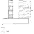
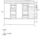
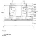
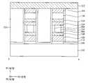
도 1은 예시적인 실시예들에 따른 가변 저항 메모리 장치를 설명하기 위한 평면도이고, 도 2 및 도 3은 상기 가변 저항 메모리 장치를 설명하기 위한 단면도들이다.
도 4 내지 도 22는 예시적인 실시예들에 따른 가변 저항 메모리 장치의 제조 방법의 단계들을 설명하기 위한 평면도들 및 단면도들이다.
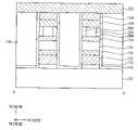
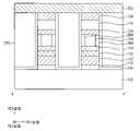
도 23은 예시적인 실시예들에 따른 가변 저항 메모리 장치를 설명하기 위한 평면도이고, 도 24 및 도 25는 상기 가변 저항 메모리 장치를 설명하기 위한 단면도들이다.
도 26 및 도 27은 예시적인 실시예들에 따른 가변 저항 메모리 장치의 제조 방법의 단계들을 설명하기 위한 평면도 및 단면도이다.
도 28은 예시적인 실시예들에 따른 가변 저항 메모리 장치를 설명하기 위한 평면도이고, 도 29 및 도 30은 상기 가변 저항 메모리 장치를 설명하기 위한 단면도들이다.
도 31 내지 도 34는 예시적인 실시예들에 따른 가변 저항 메모리 장치를 설명하기 위한 단면도들이다.
도 35 및 도 36은 예시적인 실시예들에 따른 가변 저항 메모리 장치를 설명하기 위한 단면도들이다.
도 37 및 도 38은 예시적인 실시예들에 따른 가변 저항 메모리 장치의 제조 방법의 단계들을 설명하기 위한 단면도들이다.
도 39는 예시적인 실시예들에 따른 가변 저항 메모리 장치를 포함하는 시스템을 설명하기 위한 블록도이다.
도 40은 예시적인 실시예들에 따른 가변 저항 메모리 장치를 포함하는 시스템을 설명하기 위한 블록도이다.FIG. 1 is a plan view illustrating a variable resistance memory device according to example embodiments, and FIGS. 2 and 3 are cross-sectional views illustrating the variable resistance memory device.
4 to 22 are plan views and cross-sectional views illustrating steps of a method of manufacturing a variable resistance memory device according to example embodiments.
FIG. 23 is a plan view illustrating a variable resistance memory device according to example embodiments, and FIGS. 24 and 25 are cross-sectional views illustrating the variable resistance memory device.
26 and 27 are plan views and cross-sectional views illustrating steps of a method of manufacturing a variable resistance memory device according to example embodiments.
FIG. 28 is a plan view illustrating a variable resistance memory device according to example embodiments, and FIGS. 29 and 30 are cross-sectional views illustrating the variable resistance memory device.
31 to 34 are cross-sectional views illustrating a variable resistance memory device according to example embodiments.
35 and 36 are cross-sectional views illustrating a variable resistance memory device according to example embodiments.
37 and 38 are cross-sectional views illustrating steps of a method of manufacturing a variable resistance memory device according to example embodiments.
39 is a block diagram illustrating a system including a variable resistance memory device according to example embodiments.
40 is a block diagram for describing a system including a variable resistance memory device according to example embodiments.
이하, 첨부된 도면들을 참조하여 본 발명의 바람직한 실시예들에 따른 가변 저항 메모리 장치 및 그 제조 방법에 대하여 상세하게 설명하지만, 본 발명이 하기의 실시예들에 제한되는 것은 아니며, 해당 분야에서 통상의 지식을 가진 자라면 본 발명의 기술적 사상을 벗어나지 않는 범위 내에서 본 발명을 다양한 다른 형태로 구현할 수 있을 것이다. 첨부된 도면에 있어서, 기판, 층(막), 영역, 패턴들 또는 구조물들의 치수는 본 발명의 명확성을 기하기 위하여 실제보다 확대하여 도시한 것이다. 본 발명에 있어서, 각 층(막), 영역, 전극, 패턴들 또는 구조물들이 기판, 각 층(막), 영역, 전극, 구조물들 또는 패턴들 "상에", "상부에" 또는 "하부"에 형성되는 것으로 언급되는 경우에는 각 층(막), 영역, 전극, 패턴들 또는 구조물들이 직접 기판, 각 층(막), 영역, 구조물 또는 패턴들 위에 형성되거나 아래에 위치하는 것을 의미하거나, 다른 층(막), 다른 영역, 다른 전극, 다른 패턴들 또는 다른 구조물이 기판 상에 추가적으로 형성될 수 있다. 또한, 물질, 층(막), 영역, 전극, 패턴들 또는 구조물들이 "제1", "제2" 및/또는 "예비"로 언급되는 경우, 이러한 부재들을 한정하기 위한 것이 아니라 단지 각 물질, 층(막), 영역, 전극, 패턴들 또는 구조물들을 구분하기 위한 것이다. 따라서 "제1", "제2" 및/또는 "예비"는 각 층(막), 영역, 전극, 패턴들 또는 구조물들에 대하여 각기 선택적으로 또는 교환적으로 사용될 수 있다.Hereinafter, a variable resistance memory device and a manufacturing method thereof according to preferred embodiments of the present invention will be described in detail with reference to the accompanying drawings, but the present invention is not limited to the following embodiments, and conventional Those with the knowledge of will be able to implement the present invention in various other forms without departing from the technical spirit of the present invention. In the accompanying drawings, dimensions of substrates, layers (films), regions, patterns, or structures are shown enlarged than actual dimensions for clarity of the present invention. In the present invention, each layer (film), region, electrode, pattern or structure is "on", "above" or "below" the substrate, each layer (film), region, electrode, structure or pattern. When referred to as being formed on, it means that each layer (film), region, electrode, pattern or structure is directly formed on or below the substrate, each layer (film), region, structure or pattern, or other Layers (films), other regions, other electrodes, other patterns or other structures may additionally be formed on the substrate. Also, when materials, layers (films), regions, electrodes, patterns, or structures are referred to as “first,” “second,” and/or “preliminary,” these members are not meant to be limited, but each material, It is for distinguishing layers (films), regions, electrodes, patterns or structures. Thus, "first", "second" and/or "preliminary" may be used selectively or interchangeably with respect to each layer (film), region, electrode, pattern or structure, respectively.
도 1은 예시적인 실시예들에 따른 가변 저항 메모리 장치를 설명하기 위한 평면도이고, 도 2 및 도 3은 상기 가변 저항 메모리 장치를 설명하기 위한 단면도들이다. 이때, 도 2는 도 1의 A-A'선을 따라 절단한 단면도이고, 도 3은 도 1의 B-B'선을 따라 절단한 단면도이다.FIG. 1 is a plan view illustrating a variable resistance memory device according to example embodiments, and FIGS. 2 and 3 are cross-sectional views illustrating the variable resistance memory device. At this time, FIG. 2 is a cross-sectional view taken along the line AA' of FIG. 1, and FIG. 3 is a cross-sectional view taken along the line BB' of FIG.
이하에서는 기판 상면에 실질적으로 평행하고 서로 교차하는 두 방향들을 각각 제1 및 제2 방향들로 정의하고, 상기 기판 상면에 실질적으로 수직한 방향을 제3 방향으로 정의한다. 예시적인 실시예들에 있어서, 상기 제1 및 제2 방향들은 서로 직교할 수 있다.Hereinafter, two directions that are substantially parallel to the top surface of the substrate and cross each other are defined as first and second directions, respectively, and a direction substantially perpendicular to the top surface of the substrate is defined as a third direction. In example embodiments, the first and second directions may be orthogonal to each other.
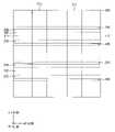
도 1 내지 도 3을 참조하면, 상기 가변 저항 메모리 장치는 기판(100) 상에 형성된 제1 도전 라인(122), 제2 도전 라인(322), 및 제1 메모리 유닛을 포함할 수 있다.1 to 3 , the variable resistance memory device may include a first
또한, 상기 가변 저항 메모리 장치는 제1 및 제2 캐핑 패턴들(245, 305), 및 제1 내지 제4 층간 절연 패턴들(112, 255, 315, 540)을 더 포함할 수 있다.Also, the variable resistance memory device may further include first and
기판(100)은 실리콘, 게르마늄, 실리콘-게르마늄과 같은 반도체 물질, 또는 GaP, GaAs, GaSb 등과 같은 Ⅲ-Ⅴ족 화합물을 포함할 수 있다. 일부 실시예들에 따르면, 기판(100)은 실리콘-온-인슐레이터(Silicon-On-Insulator: SOI) 기판 또는 게르마늄-온-인슐레이터(Germanium-On-Insulator: GOI) 기판일 수 있다.The
기판(100) 상에는 각종 소자들(도시되지 않음), 예를 들어, 게이트 구조물, 소스/드레인 층, 콘택 플러그, 배선 등이 형성될 수 있으며, 이들은 제1 층간 절연 패턴(112)에 의해 커버될 수 있다. 제1 층간 절연 패턴(112)은 예를 들어, 실리콘 산화물, 실리콘 질화물, 실리콘 산질화물 등과 같은 절연 물질을 포함할 수 있다.Various elements (not shown), for example, gate structures, source/drain layers, contact plugs, wires, and the like may be formed on the
제1 도전 라인(122)은 제1 층간 절연 패턴(112) 상에서 상기 제2 방향으로 연장될 수 있으며, 상기 제1 방향을 따라 서로 이격되도록 복수 개로 형성될 수 있다. 또한, 제2 도전 라인(322)은 제1 도전 라인(122) 상에서 이와 이격되어 상기 제1 방향으로 연장될 수 있으며, 상기 제2 방향을 따라 서로 이격되도록 복수 개로 형성될 수 있다.The first
예시적인 실시예들에 있어서, 제1 및 제2 도전 라인들(122, 322)은 각각 상기 가변 저항 메모리 장치의 워드 라인 및 비트 라인 역할을 수행할 수 있다. 이와는 달리, 제1 및 제2 도전 라인들(122, 322)은 각각 상기 가변 저항 메모리 장치의 비트 라인 및 워드 라인 역할을 수행할 수도 있다.In example embodiments, the first and second
각 제1 및 제2 도전 라인들(122, 322)은 예를 들어, 텅스텐(W), 백금(Pt), 팔라듐(Pd), 로듐(Rh), 루테늄(Ru), 이리듐(Ir), 구리(Cu), 알루미늄(Al), 티타늄(Ti), 탄탈륨(Ta) 등과 같은 금속, 혹은 이들의 금속 질화물을 포함할 수 있다.Each of the first and second
일 실시예에 있어서, 각 제1 및 제2 도전 라인들(122, 322)은 금속 패턴(도시되지 않음) 및 이의 측벽 및 저면을 커버하는 배리어 패턴(도시되지 않음)을 포함할 수 있다. 이때, 상기 금속 패턴은 예를 들어, 텅스텐(W), 백금(Pt), 팔라듐(Pd), 로듐(Rh), 루테늄(Ru), 이리듐(Ir), 구리(Cu), 알루미늄(Al), 티타늄(Ti), 탄탈륨(Ta) 등과 같은 금속을 포함할 수 있으며, 상기 배리어 패턴은 예를 들어, 티타늄 질화물, 탄탈륨 질화물, 텅스텐 질화물 등과 같은 금속 질화물을 포함할 수 있다.In one embodiment, each of the first and second
상기 제1 메모리 유닛은 제1 및 제2 도전 라인들(122, 322) 사이에서 상기 제3 방향으로 이들이 서로 오버랩되는 각 영역들에 형성될 수 있다.The first memory unit may be formed in regions where the first and second
상기 제1 메모리 유닛은 제1 전극(134), 선택 패턴(selection pattern)(144), 제2 전극 구조물(174), 절연 패턴(184), 가변 저항 패턴(294), 및 제3 전극(194)을 포함할 수 있다. 이때, 제1 전극(134), 선택 패턴(144), 제2 전극 구조물(174), 절연 패턴(184), 및 제3 전극(194)은 각 제1 도전 라인들(122) 상에 순차적으로 적층될 수 있으며, 가변 저항 패턴(270)은 제2 전극 구조물(174) 및 제3 전극(194) 사이에 형성되어 절연 패턴(184)의 측벽을 커버할 수 있다.The first memory unit includes a
각 제1 및 제3 전극들(134, 194)은 예를 들어, 티타늄 질화물(TiNx), 티타늄 실리콘 질화물(TiSiNx), 텅스텐 질화물(WNx), 텅스텐 실리콘 질화물(WSiNx), 탄탈륨 질화물(TaNx), 탄탈륨 실리콘 질화물(TaSiNx), 지르코늄 질화물(ZrNx), 지르코늄 실리콘 질화물(ZrSiNx) 등과 같은 금속 질화물 또는 금속 실리콘 질화물을 포함할 수 있다.Each of the first and
다만 경우에 따라, 제1 전극(134) 및/또는 제3 전극(194)은 형성되지 않고 생략될 수도 있다.However, in some cases, the
선택 패턴(144)은 비정질 상태에서 온도 변화에 따른 저항 차이로 인해 스위칭 역할을 수행할 수 있는 오티에스(Ovonic Threshold Switch: OTS) 물질을 포함할 수 있다. 즉, 선택 패턴(144)은 가변 저항 패턴(294)에 비해 넓은 온도 범위에서 비정질 상태를 유지할 수 있으나, 상기 비정질 상태에서도 온도 변화에 따라 큰 저항 차이를 가질 수 있다.The
상기 오티에스(OTS) 물질은 예를 들어, 게르마늄(Ge), 실리콘(Si), 비소(As) 및/또는 텔루륨(Te)을 함유할 수 있으며, 이에 더하여 셀레늄(Se) 및/또는 황(S)을 더 함유할 수도 있다.The OTS material may contain, for example, germanium (Ge), silicon (Si), arsenic (As) and/or tellurium (Te), in addition to selenium (Se) and/or sulfur (S) may be further contained.
상기 오티에스(OTS) 물질은 예를 들어, AsTeGeSiIn, GeTe, SnTe, GeSe, SnSe, AsTeGeSiSbS, AsTeGeSiIP, AsTeGeSi, As2Te3Ge, As2Se3Ge, As25(Te90Ge10)75, Te40As35Si18Ge6.75In0.25, Te28As34.5Ge15.5S22, Te39As36Si17Ge7P, As10Te21S2Ge15Se50Sb2, Si5Te34As28Ge11S21Se1, AsTeGeSiSeNS, AsTeGeSiP, AsSe, AsGeSe, AsTeGeSe, ZnTe, GeTePb, GeSeTe, AlAsTe, SeAsGeC, SeTeGeSi, GeSbTeSe, GeBiTeSe, GeAsSbSe, GeAsBiTe, GeAsBiSe, GexSe1-x 등을 포함할 수 있다.The OTS material is, for example, AsTeGeSiIn, GeTe, SnTe, GeSe, SnSe, AsTeGeSiSbS, AsTeGeSiIP, AsTeGeSi, As2 Te3 Ge, As2 Se3 Ge, As25 (Te90 Ge10 )75 , Te40 As35 Si18 Ge6.75 In0.25 , Te28 As34.5 Ge15.5 S22 , Te39 As36 Si17 Ge7 P, As10 Te21 S2 Ge15 Se50 Sb2 , Si5 Te34 As28 Ge11 S21 Se1 , AsTeGeSiSeNS, AsTeGeSiP, AsSe, AsGeSe, AsTeGeSe, ZnTe, GeTePb, GeSeTe, AlAsTe, SeAsGeC, SeTeGeSi, GeSbTeSe, GeBiTeSe, GeAsSbSe, GeAsBiTe, GeAsBiSe, Gex Se1-x , and the like. .
이와는 달리, 선택 패턴(144)은 각각 n형 및 p형 불순물들이 도핑된 폴리실리콘 막들, 즉 다이오드를 포함할 수도 있다.Alternatively, the
제2 전극 구조물(174)은 순차적으로 적층된 제1 및 제2 패턴들(154, 164)을 포함할 수 있다. 제1 패턴(154)은 제1 및 제3 전극들(134, 194)와 유사하게, 예를 들어, 티타늄 질화물(TiNx), 티타늄 실리콘 질화물(TiSiNx), 텅스텐 질화물(WNx), 텅스텐 실리콘 질화물(WSiNx), 탄탈륨 질화물(TaNx), 탄탈륨 실리콘 질화물(TaSiNx), 지르코늄 질화물(ZrNx), 지르코늄 실리콘 질화물(ZrSiNx) 등과 같은 금속 질화물 또는 금속 실리콘 질화물을 포함할 수 있다. 이에 따라, 제1 패턴(154)은 제2 전극으로 지칭될 수도 있다.The
제2 패턴(164)은 상부의 가변 저항 패턴(294)을 가열할 수 있으며, 이에 따라 가변 저항 패턴(294)의 저항이 변동될 수 있다. 제2 패턴(164)은 히터(heater)로 지칭될 수도 있다. 예시적인 실시예들에 있어서, 제2 패턴(164)은 탄소 혹은 탄소를 함유하는 금속을 포함할 수 있다. 예를 들어, 제2 패턴(164)은 탄소(C), 탄질화물(CN), 티타늄 탄질화물(TiCN) 및/또는 탄탈륨 탄질화물(TaCN)을 포함할 수 있다.The
절연 패턴(184)은 제2 전극 구조물(174)의 가운데 상면에 접촉할 수 있으며, 이에 따라 제3 전극(194)의 가운데 하면에도 접촉할 수 있다. 절연 패턴(184)은 예를 들어, 실리콘 산화물과 같은 산화물을 포함할 수 있다.The insulating
가변 저항 패턴(294)은 제2 전극 구조물(174)의 가장자리 상면에 접촉할 수 있으며, 이에 따라 제3 전극(194)의 가장자리 상면에도 접촉할 수 있다. 예시적인 실시예들에 있어서, 가변 저항 패턴(294)은 절연 패턴(184)의 측벽을 둘러싸는 링(ring) 형상을 가질 수 있다. 이때, 가변 저항 패턴(294)은 사각 링 형상, 원형 링 형상 혹은 타원 링 형상을 가질 수 있다.The
예시적인 실시예들에 있어서, 가변 저항 패턴(294)은 온도 변화에 따라 상이 변화하며, 이에 따라 그 저항이 변하는 물질을 포함하도록 형성될 수 있다. 이때, 상기 가변 저항 메모리 장치는 상변화 메모리(Phase-change Random Access Memory: PRAM) 장치일 수 있다.In example embodiments, the
일 실시예에 있어서, 가변 저항 패턴(294)은 게르마늄(Ge), 안티몬(Sb) 및/또는 텔루륨(Te)이 소정의 비율로 조합된 칼코게나이드(chalcogenide) 계열의 물질을 포함할 수 있다. 일 실시예에 있어서, 가변 저항 패턴(294)은 게르마늄-텔루륨(GeTe) 및 안티몬-텔루륨(SbTe)이 반복적으로 적층된 초격자(supper lattice)를 포함할 수 있다. 일 실시예에 있어서, 가변 저항 패턴(294)은 인듐-안티몬-텔루륨을 함유하는 아이에스티(IST), 혹은 비스무스-안티몬-텔루륨을 함유하는 비에스티(BST)를 포함할 수 있다.In one embodiment, the
예시적인 실시예들에 있어서, 가변 저항 패턴(294)은 페로브스카이트(perovskite) 계열의 물질 또는 전이 금속 산화물을 포함할 수 있다. 이때 상기 가변 저항 메모리 장치는 저항 가변 메모리(Resistive Random Access Memory: ReRAM) 장치일 수 있다.다.In example embodiments, the
상기 페로브스카이트 계열 물질의 예로서, STO(SrTiO3), BTO(BaTiO3), PCMO(Pr1-XCaXMnO3) 등을 들 수 있다. 상기 전이 금속 산화물의 예로서, 티타늄 산화물(TiOx), 지르코늄 산화물(ZrOx), 알루미늄 산화물(AlOx), 하프늄 산화물(HfOx), 탄탈륨 산화물(TaOx), 니오븀 산화물(NbOx), 코발트 산화물(CoOx), 텅스텐 산화물(WOx), 란탄 산화물(LaOx), 아연 산화물(ZnOx) 등을 들 수 있다. 이들은 단독으로 혹은 2 이상이 조합되어 사용될 수 있다.Examples of the perovskite-based material include STO (SrTiO3 ), BTO (BaTiO3 ), and PCMO (Pr1-X CaX MnO3 ). Examples of the transition metal oxide include titanium oxide (TiOx), zirconium oxide (ZrOx), aluminum oxide (AlOx), hafnium oxide (HfOx), tantalum oxide (TaOx), niobium oxide (NbOx), cobalt oxide (CoOx), tungsten oxide (WOx), lanthanum oxide (LaOx), zinc oxide (ZnOx), and the like. These may be used alone or in combination of two or more.
예시적인 실시예들에 있어서, 가변 저항 패턴(294)은 자기장 또는 스핀 전달 토크(Spin Transfer Torque: STT)에 의해 저항이 변하는 물질을 포함할 수 있다. 이때, 상기 가변 저항 메모리 장치는 자기 저항 메모리(Magnetic Random Access Memory: MRAM) 장치일 수 있다.다.In example embodiments, the
예를 들어, 가변 저항 패턴(294)은 철(Fe), 니켈(Ni), 코발트(Co), 디스프로슘(Dy), 가돌리늄(Gd) 등을 포함하는 강자성체를 포함할 수 있다.For example, the
예시적인 실시예들에 있어서, 상기 제1 메모리 유닛은 상기 제1 및 제2 방향들을 따라 각각 복수 개로 형성될 수 있으며, 이들은 상부에서 보았을 때 격자 모양으로 배치될 수 있다.In example embodiments, a plurality of first memory units may be formed along the first and second directions, and they may be arranged in a lattice shape when viewed from above.
상부에서 보았을 때, 제2 전극 구조물(174) 및 제3 전극(194)은 실질적으로 동일한 면적을 가질 수 있는 반면, 가변 저항 패턴(294)은 이들보다 작은 면적을 가질 수 있다. 이에 따라, 제2 전극 구조물(174) 내에 포함된 제2 패턴(164) 즉, 히터가 가변 저항 패턴(294)과 접촉하는 면적이 감소되어 소비 전류가 감소할 수 있다.When viewed from the top, the
제1 캐핑 패턴(245)은 상기 제1 메모리 유닛의 상기 제1 방향으로의 양 측벽들 및 기판(100) 상면을 커버할 수 있다. 제2 캐핑 패턴(305)은 상기 제1 메모리 유닛의 상기 제2 방향으로의 양 측벽들의 상부와, 제1 도전 라인(122), 제1 캐핑 패턴(245) 및 제2 층간 절연 패턴(255)의 상면들을 커버할 수 있다. 제1 및 제2 캐핑 패턴들(245, 305)은 예를 들어, 실리콘 질화물, 실리콘 산화물 등과 같은 절연 물질을 포함할 수 있다.The
제2 층간 절연 패턴(255)은 상기 제1 방향을 따라 서로 이격된 상기 제1 메모리 유닛들 사이에서 제1 캐핑 패턴(245) 상에 형성될 수 있으며, 제3 층간 절연 패턴(315)은 상기 제2 방향을 따라 서로 이격된 상기 제1 메모리 유닛들 사이에서 제2 캐핑 패턴(305) 상에 형성될 수 있다. 제4 층간 절연 패턴(540)은 제3 층간 절연 패턴(315) 및 제2 캐핑 패턴(305) 상에 형성되어 상기 제1 방향으로 연장될 수 있으며, 제2 도전 라인(322)의 양 측벽들에 접촉할 수 있다.The second
제2 내지 제4 층간 절연 패턴들(255, 315, 540)은 예를 들어, 실리콘 산화물, 실리콘 질화물, 실리콘 산질화물 등과 같은 절연 물질을 포함할 수 있다.The second to fourth
상기 가변 저항 메모리 장치는 제2 전극 구조물(174) 및 제3 전극(194) 사이에 형성된 절연 패턴(184)을 포함할 수 있으며, 가변 저항 패턴(294)은 제2 전극 구조물(174) 및 제3 전극(194) 사이에서 절연 패턴(184)의 측벽을 둘러싸도록 형성될 수 있다. 이에 따라, 가변 저항 패턴(294)은 제2 전극 구조물(174) 및 제3 전극(194)보다 작은 면적을 가질 수 있으며, 상기 가변 저항 메모리 장치의 소비 전류가 감소될 수 있다.The variable resistance memory device may include an insulating
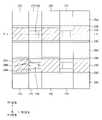
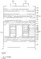
도 4 내지 도 22는 예시적인 실시예들에 따른 가변 저항 메모리 장치의 제조 방법의 단계들을 설명하기 위한 평면도들 및 단면도들이다. 구체적으로, 도 4, 7, 10, 13, 15, 17, 19, 및 21은 평면도들이고, 도 5, 6, 8, 9, 11, 12, 및 14는 대응하는 각 평면도들의 A-A'선을 따라 절단한 단면도들이며, 도 16, 18, 20, 및 22은 대응하는 각 평면도들의 B-B'선을 따라 절단한 단면도들이다.4 to 22 are plan views and cross-sectional views illustrating steps of a method of manufacturing a variable resistance memory device according to example embodiments. Specifically, FIGS. 4, 7, 10, 13, 15, 17, 19, and 21 are plan views, and FIGS. 5, 6, 8, 9, 11, 12, and 14 are corresponding plan views along line A-A'. 16, 18, 20, and 22 are cross-sectional views taken along line BB' of corresponding plan views.
도 4 및 도 5를 참조하면, 기판(100) 상에 제1 층간 절연막(110), 제1 도전막(120), 제1 전극막(130), 제1 선택막(selection layer)(140), 제2 전극막 구조물(170), 절연막(180), 제3 전극막(190) 및 제1 마스크 막(200)을 순차적으로 형성하고, 제1 마스크 막(200) 상에 제2 마스크(210)를 형성할 수 있다.4 and 5, a first
기판(100)은 실리콘, 게르마늄, 실리콘-게르마늄과 같은 반도체 물질, 또는 GaP, GaAs, GaSb 등과 같은 Ⅲ-Ⅴ족 화합물을 포함할 수 있다. 일부 실시예들에 따르면, 기판(100)은 실리콘-온-인슐레이터(SOI) 기판 또는 게르마늄-온-인슐레이터(GOI) 기판일 수 있다.The
기판(100) 상에는 각종 소자들(도시되지 않음), 예를 들어, 게이트 구조물, 콘택 플러그, 배선 등이 형성될 수 있으며, 이들은 제1 층간 절연막(110)에 의해 커버될 수 있다.Various elements (not shown), for example, gate structures, contact plugs, wires, and the like may be formed on the
제1 층간 절연막(110)은 예를 들어, 실리콘 산화물, 실리콘 질화물, 실리콘 산질화물 등과 같은 절연 물질을 포함하도록 형성될 수 있다.The first
제1 도전막(120)은 예를 들어, 텅스텐(W), 백금(Pt), 팔라듐(Pd), 로듐(Rh), 루테늄(Ru), 이리듐(Ir), 구리(Cu), 알루미늄(Al), 티타늄(Ti), 탄탈륨(Ta) 등과 같은 금속, 혹은 이들의 금속 질화물을 포함하도록 형성될 수 있다.The first
각 제1 및 제3 전극막들(130, 190)은 예를 들어, 티타늄 질화물(TiNx), 티타늄 실리콘 질화물(TiSiNx), 텅스텐 질화물(WNx), 텅스텐 실리콘 질화물(WSiNx), 탄탈륨 질화물(TaNx), 탄탈륨 실리콘 질화물(TaSiNx), 지르코늄 질화물(ZrNx), 지르코늄 실리콘 질화물(ZrSiNx) 등과 같은 금속 질화물 또는 금속 실리콘 질화물을 포함하도록 형성될 수 있다.Each of the first and
예시적인 실시예들에 있어서, 제1 선택막(140)은 비정질 상태에서 온도 변화에 따른 저항 차이로 인해 스위칭 역할을 수행할 수 있는 오티에스(OTS) 물질을 포함할 수 있다.In example embodiments, the
상기 오티에스(OTS) 물질은 예를 들어, 게르마늄(Ge), 실리콘(Si), 비소(As) 및/또는 텔루륨(Te)을 함유할 수 있으며, 이에 더하여 셀레늄(Se) 및/또는 황(S)을 더 함유할 수도 있다.The OTS material may contain, for example, germanium (Ge), silicon (Si), arsenic (As) and/or tellurium (Te), in addition to selenium (Se) and/or sulfur (S) may be further contained.
상기 오티에스(OTS) 물질은 예를 들어, AsTeGeSiIn, GeTe, SnTe, GeSe, SnSe, AsTeGeSiSbS, AsTeGeSiIP, AsTeGeSi, As2Te3Ge, As2Se3Ge, As25(Te90Ge10)75, Te40As35Si18Ge6.75In0.25, Te28As34.5Ge15.5S22, Te39As36Si17Ge7P, As10Te21S2Ge15Se50Sb2, Si5Te34As28Ge11S21Se1, AsTeGeSiSeNS, AsTeGeSiP, AsSe, AsGeSe, AsTeGeSe, ZnTe, GeTePb, GeSeTe, AlAsTe, SeAsGeC, SeTeGeSi, GeSbTeSe, GeBiTeSe, GeAsSbSe, GeAsBiTe, GeAsBiSe, GexSe1-x 등을 포함할 수 있다.The OTS material is, for example, AsTeGeSiIn, GeTe, SnTe, GeSe, SnSe, AsTeGeSiSbS, AsTeGeSiIP, AsTeGeSi, As2 Te3 Ge, As2 Se3 Ge, As25 (Te90 Ge10 )75 , Te40 As35 Si18 Ge6.75 In0.25 , Te28 As34.5 Ge15.5 S22 , Te39 As36 Si17 Ge7 P, As10 Te21 S2 Ge15 Se50 Sb2 , Si5 Te34 As28 Ge11 S21 Se1 , AsTeGeSiSeNS, AsTeGeSiP, AsSe, AsGeSe, AsTeGeSe, ZnTe, GeTePb, GeSeTe, AlAsTe, SeAsGeC, SeTeGeSi, GeSbTeSe, GeBiTeSe, GeAsSbSe, GeAsBiTe, GeAsBiSe, Gex Se1-x , and the like. .
이와는 달리, 제1 선택막(140)은 각각 n형 및 p형 불순물들이 도핑된 폴리실리콘 막들을 포함할 수도 있다.Alternatively, the
예시적인 실시예들에 있어서, 제2 전극막 구조물(170)은 제1 및 제2 층들(150, 160)을 포함할 수 있다. 이때, 제1 층(150)은 제1 및 제3 전극막들(130, 190)과 유사하게, 예를 들어, 티타늄 질화물(TiNx), 티타늄 실리콘 질화물(TiSiNx), 텅스텐 질화물(WNx), 텅스텐 실리콘 질화물(WSiNx), 탄탈륨 질화물(TaNx), 탄탈륨 실리콘 질화물(TaSiNx), 지르코늄 질화물(ZrNx), 지르코늄 실리콘 질화물(ZrSiNx) 등과 같은 금속 질화물 또는 금속 실리콘 질화물을 포함하도록 형성될 수 있으며, 이에 따라 제2 전극막으로 지칭될 수도 있다. 제2 층(160)은 탄소 혹은 탄소를 함유하는 금속을 포함할 수 있다. 예를 들어, 제2 층(160)은 탄소(C), 탄질화물(CN), 티타늄 탄질화물(TiCN) 및/또는 탄탈륨 탄질화물(TaCN)을 포함할 수 있다. 제2 층(160)은 히터막(heating layer)으로 지칭될 수도 있다.In example embodiments, the second
절연막(180)은 예를 들어, 실리콘 산화물과 같은 산화물을 포함하도록 형성될 수 있다.The insulating
제1 마스크 막(200)은 예를 들어, 실리콘 질화물과 같은 질화물을 포함하도록 형성될 수 있으며, 제2 마스크(210)는 예를 들어, 실리콘 산화물과 같은 산화물을 포함하도록 형성될 수 있다. 경우에 따라서, 제1 마스크 막(200)은 형성되지 않고 생략될 수도 있다.The
예시적인 실시예들에 있어서, 제2 마스크(210)는 상기 제2 방향으로 연장될 수 있으며, 상기 제1 방향을 따라 복수 개로 형성될 수 있다.In example embodiments, the
도 6을 참조하면, 제2 마스크(210)를 식각 마스크로 사용하여 하부의 제1 마스크 막(200)을 식각함으로써 제1 마스크(202)를 형성한 후, 제1 및 제2 마스크들(202, 210)을 식각 마스크로 사용하여 하부의 제3 전극막(190), 절연막(180), 제2 전극막 구조물(170), 선택막(140), 제1 전극막(130), 제1 도전막(120) 및 제1 층간 절연막(110)을 순차적으로 식각함으로써, 각각 예비 제3 전극(192), 예비 절연 패턴(182), 예비 제2 전극 구조물(172), 예비 선택 패턴(142), 예비 제1 전극(132), 제1 도전 라인(122) 및 제1 층간 절연 패턴(112)을 형성할 수 있다. 상기 식각 공정 중에서 제2 마스크(210)는 완전히 제거될 수도 있고, 일부가 잔류할 수도 있다.Referring to FIG. 6 , after forming the
이에 따라, 기판(100) 상에는 순차적으로 적층된 제1 층간 절연 패턴(112), 제1 도전 라인(122), 예비 제1 전극(132), 예비 선택 패턴(142), 예비 제2 전극 구조물(172), 예비 절연 패턴(182), 예비 제3 전극(192), 제1 마스크(202) 및 제2 마스크(210)를 포함하는 제1 구조물이 형성될 수 있다. 상기 제1 구조물은 상기 제2 방향으로 연장될 수 있으며, 상기 제1 방향을 따라 서로 이격되도록 복수 개로 형성될 수 있다. 이때, 상기 복수의 제1 구조물들 사이의 공간을 제1 개구(215)로 정의하기로 한다.Accordingly, on the
한편, 예비 제2 전극 구조물(172)은 순차적으로 적층된 예비 제1 패턴(152) 및 예비 제2 패턴(162)을 포함할 수 있으며, 이들은 각각 예비 제2 전극(152) 및 예비 히터(162)로 지칭될 수도 있다.Meanwhile, the preliminary
도 7 및 도 8을 참조하면, 제1 개구(215)에 의해 노출된 예비 절연 패턴(182) 부분을 제거하여 제1 갭(220)을 형성할 수 있다.Referring to FIGS. 7 and 8 , the
예시적인 실시예들에 있어서, 예비 절연 패턴(182)을 포함하는 상기 제1 구조물은 상기 제2 방향으로 연장되므로, 제1 갭(220)은 예비 절연 패턴(182)의 상기 제1 방향으로의 각 양 가장자리 부분들을 제거하여 형성될 수 있다. 이에 따라, 각 제1 갭들(220)은 상기 제2 방향으로 연장될 수 있으며, 제1 개구(215)에 연통될 수 있다.In example embodiments, since the first structure including the preliminary
예시적인 실시예들에 있어서, 제1 갭(220)은 에치 백(etch-back) 공정에 의해 형성될 수 있다.In example embodiments, the
제1 갭(220)은 이후 설명되는 예비 제1 가변 저항 패턴(232)이 형성될 공간이므로, 제1 갭(220)의 깊이를 조절함으로써 예비 제1 가변 저항 패턴(232)의 크기를 조절할 수 있다. 즉, 예비 절연 패턴(182)을 부분적으로 제거하여 형성되는 제1 갭(220)의 깊이는 제한이 없으며, 다만 예비 절연 패턴(182)이 적어도 일부라도 잔류하기만 하면 본 발명의 범위에 포함될 수 있다.Since the
도 9를 참조하면, 제1 갭(220)을 채우는 제1 가변 저항막(230)을 상기 제1 구조물의 측벽 및 상면과, 기판(100) 상면에 형성할 수 있다.Referring to FIG. 9 , a first
예시적인 실시예들에 있어서, 제1 가변 저항막(230)은 화학 기상 증착(Chemical Vapor Deposition: CVD) 공정, 원자층 증착(Atomic Layer Deposition: ALD) 등을 통해 형성될 수 있다.In example embodiments, the first
예시적인 실시예들에 있어서, 제1 가변 저항막(230)은 상변화에 따라 저항이 변하는 물질을 포함하도록 형성될 수 있다. 일 실시예에 있어서, 제1 가변 저항막(230)은 게르마늄(Ge), 안티몬(Sb) 및/또는 텔루륨(Te)이 소정의 비율로 조합된 칼코게나이드(chalcogenide) 계열의 물질을 포함할 수 있다. 일 실시예에 있어서, 제1 가변 저항막(230)은 게르마늄-텔루륨(GeTe) 및 안티몬-텔루륨(SbTe)이 반복적으로 적층된 초격자(supper lattice)를 포함할 수 있다. 일 실시예에 있어서, 제1 가변 저항막(230)은 인듐-안티몬-텔루륨을 함유하는 아이에스티(IST), 혹은 비스무스-안티몬-텔루륨을 함유하는 비에스티(BST)를 포함할 수 있다.In example embodiments, the first
예시적인 실시예들에 있어서, 제1 가변 저항막(230)은 페로브스카이트(perovskite) 계열의 물질 또는 전이 금속 산화물을 포함할 수 있다. 상기 페로브스카이트 계열 물질의 예로서, STO(SrTiO3), BTO(BaTiO3), PCMO(Pr1-XCaXMnO3) 등을 들 수 있다. 상기 전이 금속 산화물의 예로서, 티타늄 산화물(TiOx), 지르코늄 산화물(ZrOx), 알루미늄 산화물(AlOx), 하프늄 산화물(HfOx), 탄탈륨 산화물(TaOx), 니오븀 산화물(NbOx), 코발트 산화물(CoOx), 텅스텐 산화물(WOx), 란탄 산화물(LaOx), 아연 산화물(ZnOx) 등을 들 수 있다. 이들은 단독으로 혹은 2 이상이 조합되어 사용될 수 있다.In example embodiments, the first
예시적인 실시예들에 있어서, 제1 가변 저항막(230)은 자기장 또는 스핀 전달 토크(Spin Transfer Torque: STT)에 의해 저항이 변하는 물질을 포함할 수 있다. 예를 들어, 제1 가변 저항막(230)은 철(Fe), 니켈(Ni), 코발트(Co), 디스프로슘(Dy), 가돌리늄(Gd) 등을 포함하는 강자성체를 포함할 수 있다.In example embodiments, the first
도 10 및 도 11을 참조하면, 제1 가변 저항막(230)을 부분적으로 제거하여 제1 갭(220)을 채우는 예비 제1 가변 저항 패턴(232)을 형성할 수 있다.Referring to FIGS. 10 and 11 , a preliminary first
예시적인 실시예들에 있어서, 건식 식각 공정을 수행하여, 제1 가변 저항막(230) 중에서 제1 갭(220) 내에 형성된 부분을 제외한 나머지 부분을 제거함으로써 예비 제1 가변 저항 패턴(232)을 형성할 수 있다. 이때, 상기 건식 식각 공정은 제1 가변 저항막(230)만을 식각 대상으로 하는 공정이므로, 이를 적절하게 제거할 수 있는 식각 가스만을 사용하여 수행될 수 있다. 즉, 하나의 식각 공정에서 여러 가지 막들을 함께 제거하는 것이 아니라, 상기 건식 식각 공정을 통해 오직 제1 가변 저항막(230)만을 부분적으로 제거하는 것이므로, 여러 가지 종류의 식각 가스를 사용할 필요가 없다.In example embodiments, a dry etching process is performed to remove a portion of the first
예시적인 실시예들에 있어서, 예비 제1 가변 저항 패턴(232)은 상기 제2 방향으로 연장될 수 있으며, 예비 절연 패턴(182)의 상기 제1 방향으로의 각 양 측벽들에 접촉할 수 있다.In example embodiments, the preliminary first
이하에서는, 상기 제1 구조물 및 예비 제1 가변 저항 패턴(232)을 함께 제2 구조물로 지칭하기로 한다.Hereinafter, the first structure and the preliminary first
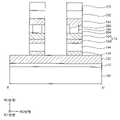
도 12를 참조하면, 상기 제2 구조물의 측벽 및 상면과, 기판(100) 상면에 제1 캐핑막(240)을 형성한 후, 제1 개구(215)의 나머지 부분을 채우는 제2 층간 절연막(250)을 제1 캐핑막(240) 상에 형성할 수 있다.Referring to FIG. 12 , after the
제1 캐핑막(240)은 예를 들어, 실리콘 질화물, 실리콘 산화물 등과 같은 절연 물질을 포함하도록 형성될 수 있다. 제2 층간 절연막(250)은 예를 들어, 실리콘 산화물과 같은 산화물을 포함하도록 형성될 수 있다.The
도 13 및 도 14를 참조하면, 예비 제3 전극(192)의 상면이 노출될 때까지 상기 제2 구조물, 제1 캐핑막(240) 및 제2 층간 절연막(250) 상부를 평탄화할 수 있다.Referring to FIGS. 13 and 14 , upper portions of the second structure, the
이에 따라, 상기 제2 구조물의 제1 및 제2 마스크들(202, 210)이 제거되어 제3 구조물이 형성될 수 있으며, 제1 캐핑막(240) 및 제2 층간 절연막(250)은 각각 제1 캐핑 패턴(245) 및 제2 층간 절연 패턴(255)로 변환될 수 있다. 이때, 제1 캐핑 패턴(245)은 상기 제2 방향으로 연장될 수 있으며, 상기 제3 구조물의 측벽 및 기판(100) 상면을 커버할 수 있다.Accordingly, the first and
예시적인 실시예들에 있어서, 상기 평탄화 공정은 화학 기계적 연마(Chemical Mechanical Polishing: CMP) 공정 및/또는 에치 백 공정을 통해 수행될 수 있다.In example embodiments, the planarization process may be performed through a chemical mechanical polishing (CMP) process and/or an etch-back process.
도 15 및 도 16을 참조하면, 상기 제3 구조물, 제1 캐핑 패턴(245) 및 제2 층간 절연 패턴(255) 상에 제3 마스크 막(260)을 형성한 후, 제3 마스크 막(260) 상에 제4 마스크(270)를 형성할 수 있다.15 and 16 , after forming a
제3 마스크 막(260)은 예를 들어, 실리콘 질화물과 같은 질화물을 포함하도록 형성될 수 있으며, 제4 마스크(270)는 예를 들어, 실리콘 산화물과 같은 산화물을 포함하도록 형성될 수 있다. 경우에 따라서, 제3 마스크 막(260)은 형성되지 않고 생략될 수도 있다.The
예시적인 실시예들에 있어서, 제4 마스크(270)는 상기 제1 방향으로 연장될 수 있으며, 상기 제2 방향을 따라 복수 개로 형성될 수 있다.In example embodiments, the
도 17 및 도 18을 참조하면, 도 6 내지 도 8을 참조로 설명한 공정들과 실질적으로 동일하거나 유사한 공정들을 수행한다.Referring to FIGS. 17 and 18 , processes substantially the same as or similar to those described with reference to FIGS. 6 to 8 are performed.
즉, 제4 마스크(270)를 식각 마스크로 사용하여 하부의 제3 마스크 막(260)을 식각함으로써 상기 제1 방향으로 연장되는 제3 마스크(262)를 형성한 후, 제3 및 제4 마스크들(262, 270)을 식각 마스크로 사용하여 하부의 예비 제3 전극(192), 예비 절연 패턴(182), 예비 제1 가변 저항 패턴(232), 예비 제2 전극 구조물(172), 예비 선택 패턴(142), 및 예비 제1 전극(132)을 순차적으로 식각함으로써, 각각 제3 전극(194), 절연 패턴(184), 제1 가변 저항 패턴(234), 제2 전극 구조물(174), 선택 패턴(144), 및 제1 전극(134)을 형성할 수 있다. 상기 식각 공정 중에서 제4 마스크(270)는 완전히 제거될 수도 있고, 일부가 잔류할 수도 있다. 이때, 제1 캐핑 패턴(245) 및 제2 층간 절연 패턴(255)의 상부도 함께 제거되어, 그 상면들의 높이가 제1 도전 라인(122)의 상면의 높이와 실질적으로 동일해질 수 있다.That is, after forming the
이에 따라, 각 제1 도전 라인(122) 상에는 순차적으로 적층된 제1 전극(134), 선택 패턴(144), 제2 전극 구조물(174), 절연 패턴(184), 제1 가변 저항 패턴(234), 제3 전극(194), 제3 마스크(262) 및 제4 마스크(270)를 포함하는 제4 구조물이 형성될 수 있다. 상기 제4 구조물은 각 제1 도전 라인(122) 상에서 상기 제2 방향을 따라 서로 이격되도록 복수 개로 형성될 수 있다. 이때, 상기 제4 구조물들 사이의 공간을 제2 개구(275)로 정의하기로 한다.Accordingly, the
한편, 제2 전극 구조물(174)은 순차적으로 적층된 제1 및 제2 패턴들(154, 164)을 포함할 수 있으며, 이들은 각각 제2 전극(154) 및 히터(164)로 지칭될 수도 있다.Meanwhile, the
이후, 제2 개구(275)에 의해 노출된 절연 패턴(184) 부분을 제거하여 제2 갭(280)을 형성할 수 있다.Thereafter, a portion of the insulating
예시적인 실시예들에 있어서, 제2 갭(280)은 절연 패턴(184)의 상기 제2 방향으로의 각 양 가장자리 부분들을 제거하여 형성될 수 있다. 이에 따라, 각 제2 갭들(280)은 제2 개구(275)에 연통될 수 있다.In example embodiments, the
예시적인 실시예들에 있어서, 제2 갭(280)은 에치 백 공정에 의해 형성될 수 있다.In example embodiments, the
도 19 및 도 20을 참조하면, 도 9 내지 도 11을 참조로 설명한 공정들과 실질적으로 동일하거나 유사한 공정들을 수행한다.Referring to FIGS. 19 and 20 , processes substantially the same as or similar to those described with reference to FIGS. 9 to 11 are performed.
즉, 제2 갭(280)을 채우는 제2 가변 저항막을 상기 제4 구조물의 측벽 및 상면과, 제1 도전 라인(122), 제1 캐핑 패턴(245) 및 제2 층간 절연 패턴(255) 상면에 형성한 후, 건식 식각 공정을 수행하여, 상기 제2 가변 저항막 중에서 제2 갭(280) 내에 형성된 부분을 제외한 나머지 부분을 제거함으로써 제2 가변 저항 패턴을 형성할 수 있다. 이때, 상기 건식 식각 공정은 상기 제2 가변 저항막만을 식각하는 공정이므로, 이를 적절하게 제거할 수 있는 식각 가스만을 사용하여 수행될 수 있다.That is, the second variable resistance film filling the
상기 제2 가변 저항 패턴은 절연 패턴(184)의 상기 제2 방향으로의 각 양 측벽들에 접촉하도록 형성될 수 있으며, 제1 가변 저항 패턴(234)에 병합될 수 있다. 서로 병합된 제1 가변 저항 패턴(234) 및 상기 제2 가변 저항 패턴은 함께 가변 저항 패턴(294)을 정의할 수 있다.The second variable resistance pattern may be formed to contact both sidewalls of the insulating
예시적인 실시예들에 있어서, 가변 저항 패턴(294)은 링 형상을 갖도록 형성될 수 있다. 일 실시예에 있어서, 가변 저항 패턴(294)은 사각 링 형상을 가질 수 있다. 이와는 달리, 가변 저항 패턴(294)은 식각 공정의 특성에 따라, 원형 링 형상 혹은 타원 링 형상을 가질 수도 있다.In example embodiments, the
한편, 상기 제4 구조물 및 가변 저항 패턴(294)은 함께 제5 구조물로 지칭하기로 한다.Meanwhile, the fourth structure and the
도 20 및 도 21을 참조하면, 도 12 내지 도 14를 참조로 설명한 공정들과 실질적으로 동일하거나 유사한 공정들을 수행한다.Referring to FIGS. 20 and 21 , processes substantially the same as or similar to those described with reference to FIGS. 12 to 14 are performed.
즉, 상기 제5 구조물의 측벽 및 상면과, 제1 도전 라인(122), 제1 캐핑 패턴(245) 및 제2 층간 절연 패턴(255) 상면에 제2 캐핑막을 형성한 후, 제2 개구(275)의 나머지 부분을 채우는 제3 층간 절연막을 상기 제2 캐핑막 상에 형성할 수 있다.That is, after forming a second capping layer on the sidewall and upper surface of the fifth structure and the upper surface of the first
상기 제2 캐핑막은 예를 들어, 실리콘 질화물, 실리콘 산화물 등과 같은 절연 물질을 포함하도록 형성될 수 있으며, 상기 제3 층간 절연막은 예를 들어, 실리콘 산화물과 같은 산화물을 포함하도록 형성될 수 있다.The second capping layer may include an insulating material such as silicon nitride or silicon oxide, and the third interlayer insulating layer may include an oxide such as silicon oxide.
이후, 제3 전극(194)의 상면이 노출될 때까지 상기 제5 구조물, 상기 제2 캐핑막 및 상기 제3 층간 절연막 상부를 평탄화함으로써, 상기 제5 구조물의 제3 및 제4 마스크들(262, 270)이 제거되어 제6 구조물이 형성될 수 있으며, 상기 제2 캐핑막 및 상기 제2 층간 절연막은 각각 제2 캐핑 패턴(305) 및 제3 층간 절연 패턴(315)로 변환될 수 있다. 이때, 제3 및 제4 마스크들(262, 270) 하부의 제1 캐핑 패턴(245) 및 제2 층간 절연 패턴(255)이 노출될 수 있다.Then, the third and
제2 캐핑 패턴(305)은 상기 제1 방향으로 연장될 수 있으며, 상기 제6 구조물의 측벽과, 제1 도전 라인(122), 제1 캐핑 패턴(245) 및 제2 층간 절연 패턴(255)의 상면을 커버할 수 있다.The
도 1 내지 도 3을 다시 참조하면, 상기 제6 구조물, 제1 캐핑 패턴(245) 및 제2 층간 절연 패턴(255) 상에 상기 제1 방향으로 연장되는 제2 도전 라인(322)을 형성한 후, 제2 캐핑 패턴(305) 및 제3 층간 절연 패턴(315) 상에 제2 도전 라인(322)의 측벽을 커버하는 제4 층간 절연 패턴(540)을 형성하여, 상기 가변 저항 메모리 장치를 완성할 수 있다.Referring back to FIGS. 1 to 3 , a second
예시적인 실시예들에 있어서, 제2 도전 라인(322)은 상기 제6 구조물, 제1 캐핑 패턴(245), 제2 층간 절연 패턴(255), 제2 캐핑 패턴(305) 및 제3 층간 절연 패턴(315) 상에 제2 도전막을 형성한 후, 상기 제1 방향으로 연장되는 식각 마스크를 사용하는 식각 공정을 통해 상기 제2 도전막을 패터닝함으로써 형성될 수 있다. 또한, 제4 층간 절연 패턴(540)은 제2 도전 라인(322)을 커버하는 제4 층간 절연막을 제2 캐핑 패턴(305) 및 제3 층간 절연 패턴(315) 상에 형성한 후, 제2 도전 라인(322)의 상면이 노출될 때까지 상기 제4 층간 절연막을 평탄화함으로써 형성될 수 있다.In example embodiments, the second
이때, 상기 제2 도전막은 예를 들어, 텅스텐(W), 백금(Pt), 팔라듐(Pd), 로듐(Rh), 루테늄(Ru), 이리듐(Ir), 구리(Cu), 알루미늄(Al), 티타늄(Ti), 탄탈륨(Ta) 등과 같은 금속, 혹은 이들의 금속 질화물을 포함하도록 형성될 수 있으며, 상기 제4 층간 절연막은 예를 들어, 실리콘 산화물과 같은 산화물을 포함하도록 형성될 수 있다.At this time, the second conductive film is, for example, tungsten (W), platinum (Pt), palladium (Pd), rhodium (Rh), ruthenium (Ru), iridium (Ir), copper (Cu), aluminum (Al) , titanium (Ti), tantalum (Ta), or metal nitrides thereof, and the fourth interlayer insulating layer may be formed to include an oxide such as silicon oxide.
이와는 달리, 제2 도전 라인(322)은 다마신 공정에 의해 형성될 수도 있다. 즉, 상기 제6 구조물, 제1 캐핑 패턴(245), 제2 층간 절연 패턴(255), 제2 캐핑 패턴(305) 및 제3 층간 절연 패턴(315) 상에 상기 제4 층간 절연막을 형성하고, 상기 제6 구조물, 제1 캐핑 패턴(245) 및 제2 층간 절연 패턴(255)의 상면을 노출시키며 상기 제1 방향으로 연장되는 제3 개구를 형성한 후, 상기 제3 개구를 채우도록 상기 제2 도전막을 상기 제6 구조물, 제1 캐핑 패턴(245), 제2 층간 절연 패턴(255) 및 상기 제4 층간 절연막 상에 형성한 다음, 상기 제4 층간 절연막 상면이 노출될 때까지 상기 제2 도전막을 평탄화함으로써 형성할 수도 있다. 예시적인 실시예들에 있어서, 다마신 공정으로 형성된 경우, 제2 도전 라인(322)은 금속 패턴(도시되지 않음) 및 이의 측벽 및 저면을 커버하는 배리어 패턴(도시되지 않음)을 포함하도록 형성될 수 있다.Alternatively, the second
한편 도시하지는 않았으나, 제2 도전 라인(322)과 마찬가지로, 제1 도전 라인(122) 역시 다마신 공정에 의해 형성될 수도 있으며, 이 경우 제1 도전 라인(122) 역시, 금속 패턴(도시되지 않음) 및 이의 측벽 및 저면을 커버하는 배리어 패턴(도시되지 않음)을 포함하도록 형성될 수 있다.Meanwhile, although not shown, like the second
전술한 바와 같이, 예시적인 실시예들에 따른 가변 저항 메모리 장치는, 제2 전극막 구조물(170) 및 제3 전극막(190) 사이에 가변 저항막을 형성하고, 이들을 포함하는 막 구조물을 동시에 식각하는 공정을 수행하여 제조되는 것이 아니라, 상기 가변 저항막 대신에 절연막(180)을 먼저 형성한 후, 이를 부분적으로 제거하여 갭들(220, 280)을 형성하고, 갭들(220, 280)을 채우도록 가변 저항 패턴(294)을 형성함으로써 제조될 수 있다. 이에 따라, 가변 저항 패턴(294)은 다른 막들과 함께 식각되지 않으므로, 다양한 식각 가스들에 노출되지 않을 수 있으며, 이에 의한 식각 손상을 받지 않을 수 있다.As described above, in the variable resistance memory device according to example embodiments, a variable resistance film is formed between the second
또한, 가변 저항 패턴(294)은 절연막(180)을 부분적으로 제거하여 형성된 갭들(220, 280)을 채우도록 형성되므로, 상기 제거 공정을 조절함으로써 원하는 크기 혹은 면적을 갖는 가변 저항 패턴(294)을 형성할 수 있다. 이에 따라, 하부에 형성되는 제2 전극 구조물(174)과의 접촉 면적을 용이하게 조절할 수 있으며, 소비 전류량을 감소시킬 수 있다.In addition, since the
도 23은 예시적인 실시예들에 따른 가변 저항 메모리 장치를 설명하기 위한 평면도이고, 도 24 및 도 25는 상기 가변 저항 메모리 장치를 설명하기 위한 단면도들이다. 이때, 도 24는 도 23의 A-A'선을 따라 절단한 단면도이고, 도 25는 도 23의 B-B'선을 따라 절단한 단면도이다.FIG. 23 is a plan view illustrating a variable resistance memory device according to example embodiments, and FIGS. 24 and 25 are cross-sectional views illustrating the variable resistance memory device. In this case, FIG. 24 is a cross-sectional view taken along the line AA' of FIG. 23, and FIG. 25 is a cross-sectional view taken along the line BB' of FIG.
상기 가변 저항 메모리 장치는 도 1 내지 도 3을 참조로 설명한 가변 저항 메모리 장치와, 절연 패턴 및 가변 저항 패턴의 형상을 제외하고는 실질적으로 동일하거나 유사하다. 이에 따라, 동일한 구성 요소에는 동일한 참조 부호를 부여하고 이에 대한 자세한 설명은 생략한다.The variable resistance memory device is substantially the same as or similar to the variable resistance memory device described with reference to FIGS. 1 to 3 except for shapes of insulating patterns and variable resistance patterns. Accordingly, the same reference numerals are assigned to the same components, and detailed descriptions thereof are omitted.
상기 가변 저항 패턴은 도 1 내지 도 3에 도시된 가변 저항 패턴(294)과는 달리, 도 17 내지 도 18을 참조로 설명한 제1 가변 저항 패턴(234)만을 포함할 수 있으며, 도 19 내지 도 20을 참조로 설명한 제2 가변 저항 패턴은 포함하지 않을 수 있다.Unlike the
이에 따라, 절연 패턴(184)은 상기 제1 메모리 유닛 내에서 상기 제2 방향으로 연장될 수 있으며, 상기 가변 저항 패턴 즉, 제1 가변 저항 패턴(234)은 절연 패턴(184)의 상기 제1 방향으로의 각 양 측벽들에 접촉할 수 있다. 즉, 상기 가변 저항 패턴은 도 1 내지 도 3에 도시된 가변 저항 패턴(294)과는 달리, 절연 패턴(184)의 모든 측벽을 둘러싸지는 않을 수 있다. 하지만, 상기 가변 저항 패턴 역시 도 1 내지 도 3에 도시된 가변 저항 패턴(294)과 유사하게 상면에서 보았을 때, 제2 전극 구조물(174) 및 제3 전극(194)의 면적보다 작은 면적을 가질 수 있다.Accordingly, the insulating
도 26 및 도 27은 예시적인 실시예들에 따른 가변 저항 메모리 장치의 제조 방법의 단계들을 설명하기 위한 평면도 및 단면도이다. 이때, 도 26은 평면도이고, 도 27은 도 26의 B-B'선을 따라 절단한 단면도이다. 상기 가변 저항 메모리 장치 제조 방법은 도 4 내지 도 22 및 도 1 내지 도 3을 참조로 설명한 공정들과 실질적으로 동일하거나 유사한 공정들을 포함하므로, 이에 대한 자세한 설명은 생략한다.26 and 27 are plan views and cross-sectional views illustrating steps of a method of manufacturing a variable resistance memory device according to example embodiments. In this case, FIG. 26 is a plan view, and FIG. 27 is a cross-sectional view taken along line BB′ of FIG. 26 . Since the method of manufacturing the variable resistance memory device includes processes substantially the same as or similar to the processes described with reference to FIGS. 4 to 22 and 1 to 3 , a detailed description thereof will be omitted.
도 26 및 도 27을 참조하면, 도 4 내지 도 18을 참조로 설명한 공정들과 실질적으로 동일하거나 유사한 공정들을 수행한다.Referring to FIGS. 26 and 27 , processes substantially the same as or similar to those described with reference to FIGS. 4 to 18 are performed.
다만, 도 17 내지 도 18을 참조하여 설명한 공정들 중에서, 제2 개구(275)에 의해 노출된 절연 패턴(184) 부분을 제거하여 제2 갭(280)을 형성하는 공정을 수행하지 않을 수 있다. 이에 따라, 절연 패턴(184)은 상기 제2 방향으로의 양 가장자리 부분이 제거되지 않고 잔류할 수 있다.However, among the processes described with reference to FIGS. 17 and 18 , the process of forming the
다시 도 23 내지 도 25를 참조하면, 도 19 내지 도 22 및 도 1 내지 도 3을 참조로 설명한 공정들과 실질적으로 동일하거나 유사한 공정들을 수행함으로써 상기 가변 저항 메모리 장치를 완성할 수 있다.Referring back to FIGS. 23 to 25 , the variable resistance memory device may be completed by performing processes substantially the same as or similar to those described with reference to FIGS. 19 to 22 and 1 to 3 .
전술한 공정들에 따르면, 예비 절연 패턴(182)의 상기 제1 방향으로의 양 가장자리 부분들은 제거하여 제1 갭들(220)은 형성하되, 상기 제2 방향으로의 양 가장자리 부분들은 제거하지 않을 수 있으며, 이에 따라 제2 갭들(280)은 형성되지 않을 수 있다. 이에 따라, 제2 전극 구조물(174) 및 제3 전극(194) 사이에는 절연 패턴(184)의 상기 제1 방향으로의 각 양 측벽들에 접촉하는 제1 가변 저항 패턴(234)만이 형성될 수 있다. 이때, 제1 가변 저항 패턴(234) 역시 도 1 내지 도 3에 도시된 가변 저항 패턴(294)과 유사하게 상면에서 보았을 때, 제2 전극 구조물(174) 및 제3 전극(194)의 면적보다 작은 면적을 가질 수 있다.According to the foregoing processes, the
도 28은 예시적인 실시예들에 따른 가변 저항 메모리 장치를 설명하기 위한 평면도이고, 도 29 및 도 30은 상기 가변 저항 메모리 장치를 설명하기 위한 단면도들이다. 이때, 도 29는 도 28의 A-A'선을 따라 절단한 단면도이고, 도 30은 도 28의 B-B'선을 따라 절단한 단면도이다.FIG. 28 is a plan view illustrating a variable resistance memory device according to example embodiments, and FIGS. 29 and 30 are cross-sectional views illustrating the variable resistance memory device. In this case, FIG. 29 is a cross-sectional view taken along the line AA' of FIG. 28, and FIG. 30 is a cross-sectional view taken along the line BB' of FIG.
상기 가변 저항 메모리 장치는 도 1 내지 도 3을 참조로 설명한 가변 저항 메모리 장치와, 절연 패턴 및 가변 저항 패턴의 형상을 제외하고는 실질적으로 동일하거나 유사하다. 이에 따라, 동일한 구성 요소에는 동일한 참조 부호를 부여하고 이에 대한 자세한 설명은 생략한다.The variable resistance memory device is substantially the same as or similar to the variable resistance memory device described with reference to FIGS. 1 to 3 except for shapes of insulating patterns and variable resistance patterns. Accordingly, the same reference numerals are assigned to the same components, and detailed descriptions thereof are omitted.
절연 패턴(186)은 상기 제1 메모리 유닛 내에서 상기 제1 방향으로 연장될 수 있으며, 가변 저항 패턴(236)은 절연 패턴(186)의 상기 제2 방향으로의 각 양 측벽들에 접촉할 수 있다. 즉, 가변 저항 패턴(236)은 도 1 내지 도 3에 도시된 가변 저항 패턴(294)과는 달리, 절연 패턴(186)의 모든 측벽을 둘러싸지는 않을 수 있다. 하지만, 가변 저항 패턴(186) 역시 도 1 내지 도 3에 도시된 가변 저항 패턴(294)과 유사하게 상면에서 보았을 때, 제2 전극 구조물(174) 및 제3 전극(194)의 면적보다 작은 면적을 가질 수 있다.The insulating
도 31 내지 도 34는 예시적인 실시예들에 따른 가변 저항 메모리 장치를 설명하기 위한 단면도들이다. 상기 각 가변 저항 메모리 장치들은 선택 패턴 및 히터의 위치를 제외하고는, 도 1 내지 도 3을 참조로 설명한 가변 저항 메모리 장치와 실질적으로 동일하거나 유사하다. 이에 따라, 동일한 구성 요소에는 동일한 참조 부호를 부여하고, 이에 대한 자세한 설명은 생략한다.31 to 34 are cross-sectional views illustrating a variable resistance memory device according to example embodiments. Each of the variable resistance memory devices is substantially the same as or similar to the variable resistance memory device described with reference to FIGS. 1 to 3 except for a selection pattern and a location of a heater. Accordingly, the same reference numerals are given to the same components, and detailed description thereof will be omitted.
먼저 도 31을 참조하면, 절연 패턴(184) 및 가변 저항 패턴(294) 하부에는 제1 패턴(154) 즉, 제2 전극(154)이 형성되며, 절연 패턴(184) 및 가변 저항 패턴(294) 상부에는 제2 패턴(164) 즉, 히터(164)가 형성되고, 히터(164) 상에 제3 전극(194)이 형성될 수 있다.Referring first to FIG. 31 , a
이에 따라, 순차적으로 적층된 히터(164) 및 제3 전극(194)이 제3 전극 구조물을 형성할 수 있으며, 상기 제3 전극 구조물에 포함된 히터(164)가 하부의 가변 저항 패턴(294)을 가열하여 그 저항을 변동시킬 수 있다.Accordingly, the sequentially
도 32를 참조하면, 제1 전극(134) 상에 제2 패턴(164) 즉 히터(164)가 형성될 수 있으며, 히터(164) 상에 절연 패턴(184) 및 가변 저항 패턴(294)이 형성될 수 있다. 이에 따라, 순차적으로 적층된 제1 전극(134) 및 히터(164)가 제1 전극 구조물을 형성할 수 있으며, 상기 제1 전극 구조물에 포함된 히터(164)가 상부의 가변 저항 패턴(294)을 가열하여 그 저항을 변동시킬 수 있다.Referring to FIG. 32 , a
한편, 절연 패턴(184) 및 가변 저항 패턴(294) 상부에는 제1 패턴(154) 즉 제2 전극(154)이 형성될 수 있으며, 제2 전극(154)과 제3 전극(194) 사이에는 선택 패턴(144)이 형성될 수 있다.Meanwhile, the
도 33을 참조하면, 제1 전극(134) 상에 절연 패턴(184) 및 가변 저항 패턴(294)이 형성될 수 있다. 또한, 절연 패턴(184) 및 가변 저항 패턴(294) 상부에 제2 패턴(164) 즉 히터(164)가 형성될 수 있으며, 히터(164) 상에 제1 패턴(154) 즉 제2 전극(154)이 형성될 수 있다. 이에 따라, 순차적으로 적층된 히터(164) 및 제2 전극(154)이 제2 전극 구조물을 형성할 수 있으며, 상기 제2 전극 구조물에 포함된 히터(164)가 하부의 가변 저항 패턴(294)을 가열하여 그 저항을 변동시킬 수 있다.Referring to FIG. 33 , an insulating
한편, 상기 제2 전극 구조물과 제3 전극(194) 사이에는 선택 패턴(144)이 형성될 수 있다.Meanwhile, a
도 34를 참조하면, 제2 전극 구조물이 단일층으로 형성될 수 있다. 예시적으로 도 34에는 상기 제2 전극 구조물이 제1 패턴(154) 즉 제2 전극(154)만을 포함하는 것이 도시되어 있다. 이 경우, 가변 저항 패턴(294)은 별도의 히터 없이 자체 발열될 수 있다.Referring to FIG. 34 , the second electrode structure may be formed as a single layer. As an example, FIG. 34 shows that the second electrode structure includes only the
이와는 달리, 상기 제2 전극 구조물은 제2 패턴(도시되지 않음) 즉 히터만으로 형성될 수도 있다.Alternatively, the second electrode structure may be formed of only a second pattern (not shown), that is, a heater.
도 35 및 도 36은 예시적인 실시예들에 따른 가변 저항 메모리 장치를 설명하기 위한 단면도들이다. 상기 가변 저항 메모리 장치는 도 1 내지 도 3을 참조로 설명한 가변 저항 메모리 장치를 수직적으로 적층하여 제조된 것이다. 이에 따라, 동일한 구성 요소에는 동일한 참조 부호를 부여하고 이에 대한 자세한 설명은 생략한다.35 and 36 are cross-sectional views illustrating a variable resistance memory device according to example embodiments. The variable resistance memory device is manufactured by vertically stacking the variable resistance memory devices described with reference to FIGS. 1 to 3 . Accordingly, the same reference numerals are assigned to the same components, and detailed descriptions thereof are omitted.
도 35 및 도 36을 참조하면, 상기 가변 저항 메모리 장치는 상기 제3 방향으로 적층된 제1 및 제2 메모리 구조물들을 포함할 수 있다. 이때, 상기 각 제1 및 제2 메모리 구조물들은 도 1 내지 도 3에 도시된 가변 저항 메모리 장치와 실질적으로 동일할 수 있다. 다만, 상기 제1 및 제2 메모리 구조물들은 제2 도전 라인(322)을 서로 공유할 수 있다. 즉, 상기 제1 및 제2 메모리 구조물들을 포함하는 상기 가변 저항 메모리 장치는 하나의 제2 도전 라인(322)만을 포함할 수 있다.Referring to FIGS. 35 and 36 , the variable resistance memory device may include first and second memory structures stacked in the third direction. In this case, each of the first and second memory structures may be substantially the same as the variable resistance memory device shown in FIGS. 1 to 3 . However, the first and second memory structures may share the second
이에 따라, 상기 제1 메모리 구조물은 제1 및 제2 도전 라인들(122, 322), 및 상기 제3 방향을 따라 이들이 서로 오버랩되는 영역들에 각각 형성된 복수의 제1 메모리 유닛들을 포함할 수 있으며, 상기 각 제1 메모리 유닛들은 순차적으로 적층된 제1 전극(134), 선택 패턴(144), 제2 전극 구조물(174), 절연 패턴(184), 및 제3 전극(194)을 포함할 수 있다. 또한 상기 각 제1 메모리 유닛들은, 제2 전극 구조물(174)과 제3 전극(194) 사이에 형성되어 절연 패턴(184)의 측벽을 둘러싸는 가변 저항 패턴(294)을 더 포함할 수 있다. 이때, 제2 전극 구조물(174)은 순차적으로 적층된 제1 및 제2 패턴들(154, 164)을 포함할 수 있다.Accordingly, the first memory structure may include first and second
상기 제2 메모리 구조물은 제2 및 제1 도전 라인들(322, 522), 및 상기 제3 방향을 따라 이들이 서로 오버랩되는 영역들에 각각 형성된 복수의 제2 메모리 유닛들을 포함할 수 있으며, 상기 각 제2 메모리 유닛들은 순차적으로 적층된 제1 전극(334), 선택 패턴(344), 제2 전극 구조물(374), 절연 패턴(384), 및 제3 전극(394)을 포함할 수 있다. 또한 상기 각 제2 메모리 유닛들은, 제2 전극 구조물(374)과 제3 전극(394) 사이에 형성되어 절연 패턴(384)의 측벽을 둘러싸는 가변 저항 패턴(494)을 더 포함할 수 있다. 이때, 제2 전극 구조물(374)은 순차적으로 적층된 제1 및 제2 패턴들(354, 364)을 포함할 수 있다.The second memory structure may include second and first
예시적인 실시예들에 있어서, 각 제1 도전 라인들(122, 522)은 상기 제2 방향으로 연장되면서 상기 제1 방향을 따라 복수 개로 형성될 수 있으며, 제2 도전 라인(322)은 상기 제1 방향으로 연장되면서 상기 제2 방향을 따라 복수 개로 형성될 수 있다.In example embodiments, each of the first
다만, 절연 패턴(184) 및 가변 저항 패턴(294)의 형상은 도 1 내지 도 3에 도시된 것뿐만 아니라, 도 23 내지 도 25 혹은 도 28 내지 도 30에 도시된 형상을 가질 수도 있다. 또한, 가변 저항 패턴(294) 및 선택 패턴(144)의 위치는 도 1 내지 도 3에 도시된 것뿐만 아니라, 도 31 내지 도 34에 도시된 위치를 가질 수도 있다.However, the shapes of the insulating
예시적인 실시예들에 있어서, 각 제1 도전 라인들(122, 522)은 워드 라인 역할을 수행할 수 있으며, 제2 도전 라인(322)은 비트 라인 역할을 수행할 수 있다. 이와는 반대로, 각 제1 도전 라인들(122, 522)은 비트 라인 역할을 수행할 수 있으며, 제2 도전 라인(322)은 워드 라인 역할을 수행할 수도 있다.In example embodiments, each of the first
도 35 및 도 36에서는 예시적으로 상하부에 2개의 층으로 적층된 제1 및 제2 메모리 구조물들을 포함하는 가변 저항 메모리 장치를 도시하였으나, 본 발명의 개념은 이에 한정되지는 않으며, 상기 가변 저항 메모리 장치는 상기 제3 방향으로 임의의 복수의 층들에 형성된 메모리 구조물들을 포함할 수 있다.35 and 36 exemplarily illustrate a variable resistance memory device including first and second memory structures stacked in two layers on top and bottom sides, but the concept of the present invention is not limited thereto, and the variable resistance memory device is not limited thereto. The device may include memory structures formed in any of a plurality of layers in the third direction.
도 37 및 도 38은 예시적인 실시예들에 따른 가변 저항 메모리 장치의 제조 방법의 단계들을 설명하기 위한 단면도들이다. 상기 가변 저항 메모리 장치 제조 방법은 도 4 내지 도 22 및 도 1 내지 도 3을 참조로 설명한 공정들과 실질적으로 동일하거나 유사한 공정들을 포함하므로, 이에 대한 자세한 설명은 생략한다.37 and 38 are cross-sectional views illustrating steps of a method of manufacturing a variable resistance memory device according to example embodiments. Since the method of manufacturing the variable resistance memory device includes processes substantially the same as or similar to the processes described with reference to FIGS. 4 to 22 and 1 to 3 , a detailed description thereof will be omitted.
도 37 및 도 38을 참조하면, 먼저 도 4 내지 도 22를 참조로 설명한 공정들과 실질적으로 동일하거나 유사한 공정들을 수행하여 상기 제1 메모리 유닛을 포함하는 제1 메모리 구조물을 형성한다. 다만, 제2 도전 라인(322) 및 제4 층간 절연 패턴(540)은 형성하지 않는다.Referring to FIGS. 37 and 38 , processes substantially the same as or similar to those described with reference to FIGS. 4 to 22 are performed to form a first memory structure including the first memory unit. However, the second
이후, 도 4 및 도 5를 참조로 설명한 공정들과 실질적으로 동일하거나 유사한 공정들을 수행함으로써, 상기 제1 메모리 구조물 상에 제1 도전막(320), 제1 전극막(330), 제1 선택막(340), 제2 전극막 구조물(370), 절연막(380), 제3 전극막(390) 및 제1 마스크 막(400)을 순차적으로 형성하고, 제1 마스크 막(400) 상에 제2 마스크(410)를 형성할 수 있다.Thereafter, by performing processes substantially the same as or similar to those described with reference to FIGS. 4 and 5 , the first
이때, 제2 마스크(410)은 상기 제1 방향을 따라 연장될 수 있으며, 상기 제1 메모리 구조물에 포함된 상기 제1 메모리 유닛과 상기 제3 방향으로 수직적으로 오버랩되도록 형성될 수 있다.In this case, the
도 38을 참조하면, 도 6 내지 도 14를 참조로 설명한 공정들과 실질적으로 동일하거나 유사한 공정들을 수행함으로써, 상기 제1 방향으로 배치된 복수의 제1 메모리 유닛들 상에 상기 제1 방향으로 연장되며, 순차적으로 적층된 제1 도전 라인(322), 예비 제1 전극(332), 예비 선택 패턴(342), 예비 제2 전극 구조물(372), 예비 절연 패턴(382), 예비 제1 가변 저항 패턴(382) 및 예비 제3 전극(392)을 포함하는 제3 구조물을 형성할 수 있으며, 상기 제3 구조물의 상기 제2 방향으로의 측벽들과, 하부의 상기 제1 메모리 구조물에 포함된 제3 층간 절연 패턴(315) 및 제2 캐핑 패턴(305)의 상면들을 커버하는 제1 캐핑 패턴(445) 및 제2 층간 절연 패턴(455)을 형성할 수 있다.Referring to FIG. 38 , by performing processes substantially the same as or similar to those described with reference to FIGS. 6 to 14 , the plurality of first memory units disposed in the first direction extend in the first direction. and sequentially stacked first
다시 도 35 및 도 36을 참조하면, 도 15 내지 도 22 및 도 1 내지 도 3을 참조로 설명한 공정들과 실질적으로 동일하거나 유사한 공정들을 수행함으로써, 상기 가변 저항 메모리 장치를 완성할 수 있다.Referring back to FIGS. 35 and 36 , the variable resistance memory device may be completed by performing processes substantially the same as or similar to those described with reference to FIGS. 15 to 22 and 1 to 3 .
도 39는 예시적인 실시예들에 따른 가변 저항 메모리 장치를 포함하는 시스템을 설명하기 위한 블록도이다.39 is a block diagram illustrating a system including a variable resistance memory device according to example embodiments.
도 39를 참조하면, 시스템(600)은 컨트롤러(CONTROLLER, 610), 메모리 장치(MEMORY DEVICE, 620), 입출력 장치(I/O DEVICE, 630), 및 무선 인터페이스(WIRELESS INTERFACE, 640)를 포함할 수 있으며, 이들은 예를 들어, 버스(bus, 650)를 통해 서로 연결될 수 있다.Referring to FIG. 39, a
컨트롤러(610)는 예를 들어, 마이크로프로세서(microprocessor), 디지털 신호 프로세서(digital signal processor), 마이크로컨트롤러(microcontroller) 등을 포함할 수 있다.The
메모리 장치(620)는 시스템(600)으로 전송되거나 혹은 시스템(600)에 의해 전송되는 메시지, 데이터 등을 저장할 수 있다. 예시적인 실시예들에 있어서, 메모리 장치(620)는 도 1 내지 도 38을 참조로 설명한 가변 저항 메모리 장치를 포함할 수 있다.The
입출력 장치(630)는 사용자에 의해 메시지, 데이터 등을 생성하는 데 사용될 수 있다.Input/
무선 인터페이스(640)는 무선 주파수(radio frequency: RF)를 통해 무선 통신 네트워크와 메시지, 데이터 등을 주고 받는 데 사용될 수 있다. 무선 인터페이스(640)는 예를 들어, 안테나(antenna), 무선 트랜시버(transceiver) 등을 포함할 수 있다.The
도 40은 예시적인 실시예들에 따른 가변 저항 메모리 장치를 포함하는 시스템을 설명하기 위한 블록도이다.40 is a block diagram for describing a system including a variable resistance memory device according to example embodiments.
도 40을 참조하면, 시스템(700)은 중앙처리장치(CPU) 패키지(710) 및 듀얼 인라인 메모리 모듈(Dual Inline Memory Module: DIMM, 770)을 포함할 수 있다.Referring to FIG. 40 , a
예시적인 실시예들에 있어서, CPU 패키지(710)는 프로세서(PROCESSOR)(720), 및 적어도 하나 이상의 디램(Dynamic Random Access Memory: DRAM) 장치(750)를 포함할 수 있다. DRAM 장치(750)는 예를 들어, 고대역 링크(760)를 통해 프로세서(720)에 연결될 수 있다.In example embodiments, the
프로세서(720)는 내부에 집적 메모리 컨트롤러(Integrated Memory Controller: IMC)(730) 및 메모리 사이드 캐시 컨트롤러(Memory Side Cache Controller: MSC CTRL)(740)를 포함할 수 있다.The
DIMM(770)은 예를 들어, 디디알 프로토콜(DDR protocol) 및 트랜잭션 프로토콜(transactional protocol)을 전달할 수 있는 디디알(DDR) 채널(780)을 통해 CPU 패키지(710)와 통신할 수 있는 가변 저항 메모리 장치를 포함할 수 있다. 예시적인 실시예들에 있어서, 상기 가변 저항 메모리는 도 1 내지 도 38을 참조로 설명한 가변 저항 메모리 장치일 수 있다.The
예시적인 실시예들에 따른 가변 저항 메모리 장치는 상변화 메모리(PRAM) 장치, 저항 가변 메모리(ReRAM) 장치, 자기 저항 메모리(MRAM) 장치 등에 사용될 수 있다.A variable resistance memory device according to example embodiments may be used for a phase change memory (PRAM) device, a resistance variable memory (ReRAM) device, a magnetoresistive memory (MRAM) device, and the like.
상술한 바와 같이 본 발명의 바람직한 실시예들을 참조하여 설명하였지만 해당 기술 분야에서 통상의 지식을 가진 자라면 특허 청구 범위에 기재된 본 발명의 사상 및 영역으로부터 벗어나지 않는 범위 내에서 본 발명을 다양하게 수정 및 변경시킬 수 있음을 이해할 수 있을 것이다.As described above, it has been described with reference to the preferred embodiments of the present invention, but those skilled in the art can variously modify and modify the present invention within the scope not departing from the spirit and scope of the present invention described in the claims. You will understand that it can be changed.
100: 기판110, 250: 제1, 제2 층간 절연막
112, 255, 315, 540: 제1 내지 제4 층간 절연 패턴
122, 522: 제1 도전 라인322: 제2 도전 라인
130, 190: 제1, 제3 전극막170: 제2 전극막 구조물
132, 192: 예비 제1, 제3 전극172: 예비 제2 전극 구조물
134, 194: 제1, 제3 전극174: 제2 전극 구조물
140: 선택막142: 예비 선택 패턴
144: 선택 패턴150, 160: 제1, 제2 층
152, 162: 예비 제1, 제2 패턴154, 164: 제1, 제2 패턴
180: 절연막182: 예비 절연 패턴
184: 절연 패턴200: 제1 마스크 막
202, 210: 제1, 제2 마스크215, 275: 제1, 제2 개구
245, 305: 제1, 제2 캐핑 패턴260: 제3 마스크 막
262, 270: 제3, 제4 마스크220, 280: 제1, 제2 갭100:
112, 255, 315, 540: first to fourth interlayer insulating patterns
122, 522: first conductive line 322: second conductive line
130, 190: first and third electrode films 170: second electrode film structure
132, 192: preliminary first and third electrodes 172: preliminary second electrode structure
134, 194: first and third electrodes 174: second electrode structure
140: selection film 142: preliminary selection pattern
144: selected
152, 162: preliminary first and
180: insulating film 182: preliminary insulating pattern
184: insulating pattern 200: first mask film
202, 210: first and
245, 305: first and second capping patterns; 260: third mask layer;
262, 270: third and
Claims (20)
Translated fromKorean상기 제1 도전 라인들 상에서 각각이 상기 제1 방향으로 연장되며, 상기 제2 방향을 따라 복수 개로 형성된 제2 도전 라인들;
상기 제1 및 제2 도전 라인들 사이에서 상기 기판 상면에 수직한 제3 방향으로 이들이 서로 오버랩되는 각 영역들에 형성되며,
전극 구조물;
상기 전극 구조물의 중앙부 상면에 형성된 절연 패턴; 및
상기 전극 구조물의 가장자리 상면에 형성되어 상기 절연 패턴의 측벽에 접촉하는 가변 저항 패턴을 포함하는 메모리 유닛;
상기 메모리 유닛의 상기 제1 및 제2 방향으로의 양 측벽들, 상기 기판의 상면 및 상기 제1 도전 라인의 상면 상에 형성된 캐핑 패턴; 및
상기 제1 및 제2 방향을 따라 서로 이격된 상기 메모리 유닛들 사이에서 상기 캐핑 패턴 상에 형성된 층간 절연 패턴을 구비하는 가변 저항 메모리 장치.first conductive lines each extending in a second direction parallel to the top surface of the substrate and formed in plurality along a first direction that is parallel to the top surface of the substrate and intersects the second direction;
second conductive lines each extending in the first direction on the first conductive lines and formed in plurality along the second direction;
formed in respective regions overlapping each other in a third direction perpendicular to the upper surface of the substrate between the first and second conductive lines;
electrode structure;
an insulating pattern formed on an upper surface of the central portion of the electrode structure; and
a memory unit including a variable resistance pattern formed on an upper surface of an edge of the electrode structure and contacting a sidewall of the insulating pattern;
a capping pattern formed on both sidewalls of the memory unit in the first and second directions, an upper surface of the substrate, and an upper surface of the first conductive line; and
A variable resistance memory device comprising an interlayer insulating pattern formed on the capping pattern between the memory units spaced apart from each other along the first and second directions.
제2 전극; 및
상기 제2 전극 상에 형성된 히터(heater)를 포함하는 가변 저항 메모리 장치.The method of claim 1, wherein the electrode structure,
a second electrode; and
A variable resistance memory device comprising a heater formed on the second electrode.
상기 선택 패턴 하부에 형성된 제1 전극; 및
상기 절연 패턴 및 상기 가변 저항 패턴 상부에 형성된 제3 전극을 더 포함하는 가변 저항 메모리 장치.According to claim 7,
a first electrode formed under the selection pattern; and
The variable resistance memory device further comprising a third electrode formed on the insulating pattern and the variable resistance pattern.
제1 전극; 및
상기 제1 전극 상에 형성된 히터를 포함하는 가변 저항 메모리 장치.The method of claim 1, wherein the electrode structure,
a first electrode; and
A variable resistance memory device comprising a heater formed on the first electrode.
상기 제1 도전 라인들 상에서 각각이 상기 제1 방향으로 연장되며, 상기 제2 방향을 따라 복수 개로 형성된 제2 도전 라인들;
상기 제1 및 제2 도전 라인들 사이에서 상기 기판 상면에 수직한 제3 방향으로 이들이 서로 오버랩되는 각 영역들에 형성되며,
전극 구조물;
상기 전극 구조물의 중앙부 하면에 접촉하는 절연 패턴; 및
상기 전극 구조물의 가장자리 하면에 접촉하며 상기 절연 패턴의 측벽에 접촉하는 가변 저항 패턴을 포함하는 메모리 유닛;
상기 메모리 유닛의 상기 제1 및 제2 방향으로의 양 측벽들, 상기 기판의 상면 및 상기 제1 도전 라인의 상면 상에 형성된 캐핑 패턴; 및
상기 제1 및 제2 방향을 따라 서로 이격된 상기 메모리 유닛들 사이에서 상기 캐핑 패턴 상에 형성된 층간 절연 패턴을 구비하는 가변 저항 메모리 장치.first conductive lines each extending in a second direction parallel to the top surface of the substrate and formed in plurality along a first direction that is parallel to the top surface of the substrate and intersects the second direction;
second conductive lines each extending in the first direction on the first conductive lines and formed in plurality along the second direction;
formed in respective regions overlapping each other in a third direction perpendicular to the upper surface of the substrate between the first and second conductive lines;
electrode structure;
an insulating pattern contacting the lower surface of the central portion of the electrode structure; and
a memory unit including a variable resistance pattern contacting a lower edge of the electrode structure and contacting a sidewall of the insulating pattern;
a capping pattern formed on both sidewalls of the memory unit in the first and second directions, an upper surface of the substrate, and an upper surface of the first conductive line; and
A variable resistance memory device comprising an interlayer insulating pattern formed on the capping pattern between the memory units spaced apart from each other along the first and second directions.
상기 제1 전극 상의 선택 패턴;
상기 선택 패턴 상의 제2 전극;
상기 제2 전극의 가운데 상면에 형성된 절연 패턴;
상기 제2 전극의 가장자리 상면에 형성되어 상기 절연 패턴의 적어도 일부 측벽을 커버하는 가변 저항 패턴;
상기 절연 패턴 및 상기 가변 저항 패턴 상의 제3 전극을 포함하는 메모리 유닛;
상기 메모리 유닛의 측벽, 상기 기판의 상면 상에 형성된 캐핑 패턴; 및
서로 이격된 상기 메모리 유닛들 사이에서 상기 캐핑 패턴 상에 형성된 층간 절연 패턴을 구비하는 가변 저항 메모리 장치.a first electrode on the substrate;
a selection pattern on the first electrode;
a second electrode on the selected pattern;
an insulating pattern formed on a central upper surface of the second electrode;
a variable resistance pattern formed on an upper surface of an edge of the second electrode to cover at least a portion of a sidewall of the insulating pattern;
a memory unit including a third electrode on the insulating pattern and the variable resistance pattern;
a capping pattern formed on a sidewall of the memory unit and an upper surface of the substrate; and
A variable resistance memory device comprising an interlayer insulating pattern formed on the capping pattern between the memory units spaced apart from each other.
상기 제2 전극막, 상기 절연막 및 상기 제1 전극막 구조물을 패터닝하여 각각 제2 전극, 절연 패턴 및 제1 전극 구조물을 형성하고;
상기 절연 패턴의 가장자리 부분을 제거하여 상기 제1 전극 구조물 및 상기 제2 전극 사이에 갭을 형성하고;
상기 갭을 채우는 가변 저항막을 상기 절연 패턴, 상기 제1 전극 구조물 및 상기 제2 전극의 측벽 상에 형성하고; 그리고
상기 가변 저항막을 선택적으로 제거할 수 있는 식각 가스를 이용하여 상기 제1 전극 구조물 및 상기 제2 전극의 측벽이 노출되도록 상기 가변 저항막을 식각하여 가변 저항 패턴을 형성하는 것을 포함하는 가변 저항 메모리 장치의 제조 방법.sequentially stacking a first electrode film structure, an insulating film and a second electrode film on the substrate;
patterning the second electrode film, the insulating film, and the first electrode film structure to form a second electrode, an insulating pattern, and a first electrode structure, respectively;
forming a gap between the first electrode structure and the second electrode by removing an edge portion of the insulating pattern;
forming a variable resistance film filling the gap on sidewalls of the insulating pattern, the first electrode structure, and the second electrode; And
and forming a variable resistance pattern by etching the variable resistance film to expose sidewalls of the first electrode structure and the second electrode using an etching gas capable of selectively removing the variable resistance film. manufacturing method.
상기 기판 상면에 평행한 제2 방향으로 연장되는 제1 식각 마스크를 사용하여 상기 제2 전극막, 상기 절연막 및 상기 제1 전극막 구조물을 식각함으로써, 각각 예비 제2 전극, 예비 절연 패턴 및 예비 제1 전극 구조물을 형성하고; 그리고
상기 기판 상면에 평행하고 상기 제2 방향과 교차하는 제1 방향으로 연장되는 제2 식각 마스크를 사용하여 상기 예비 제2 전극, 상기 예비 절연 패턴 및 상기 예비 제1 전극 구조물을 식각함으로써, 각각 상기 제2 전극, 상기 절연 패턴 및 상기 제1 전극 구조물을 형성하는 것을 포함하는 가변 저항 메모리 장치의 제조 방법.The method of claim 15, wherein forming the second electrode, the insulating pattern, and the first electrode structure by patterning the second electrode film, the insulating film, and the first electrode film structure, respectively,
The second electrode film, the insulating film, and the first electrode film structure are etched using a first etching mask extending in a second direction parallel to the upper surface of the substrate, so that the preliminary second electrode, the preliminary insulating pattern, and the preliminary second electrode film structure are etched. forming one electrode structure; And
The preliminary second electrode, the preliminary insulating pattern, and the preliminary first electrode structure are etched using a second etching mask extending in a first direction parallel to the upper surface of the substrate and intersecting the second direction, respectively. A method of manufacturing a variable resistance memory device comprising forming two electrodes, the insulating pattern, and the first electrode structure.
상기 예비 제2 전극, 상기 예비 절연 패턴 및 상기 예비 제1 전극 구조물을 식각하기 이전에,
상기 예비 절연 패턴의 상기 제1 방향으로의 양 가장자리 부분들을 제거하여 상기 제1 갭들을 각각 형성하고; 그리고
상기 제1 갭들을 각각 채우는 상기 제1 가변 저항 패턴을 형성하는 것을 포함하는 가변 저항 메모리 장치의 제조 방법18. The method of claim 17, wherein the gap includes first and second gaps, and the variable resistance pattern includes first and second variable resistance patterns,
Before etching the preliminary second electrode, the preliminary insulating pattern, and the preliminary first electrode structure,
forming the first gaps by removing both edge portions of the preliminary insulating pattern in the first direction; And
A method of manufacturing a variable resistance memory device comprising forming the first variable resistance pattern to fill the first gaps, respectively.
상기 예비 제2 전극, 상기 제1 가변 저항 패턴 및 상기 예비 제1 전극 구조물의 측벽을 커버하는 제1 캐핑막을 형성하는 것을 더 포함하는 가변 저항 메모리 장치의 제조 방법.19. The method of claim 18, after forming the first variable resistance pattern filling the first gaps, respectively,
The method of manufacturing the variable resistance memory device further comprising forming a first capping layer covering sidewalls of the preliminary second electrode, the first variable resistance pattern, and the preliminary first electrode structure.
상기 기판 상면에 평행한 제2 방향으로 연장되는 제1 식각 마스크를 사용하여 상기 제2 전극막, 상기 절연막 및 상기 제1 전극막을 패터닝하여 각각 예비 제2 전극, 예비 절연 패턴 및 예비 제1 전극을 형성하고;
상기 기판 상면에 평행하고 상기 제2 방향에 실질적으로 수직한 제1 방향으로의 상기 예비 절연 패턴의 양 가장자리들을 제거하여 각각 제1 갭들을 형성하고;
상기 각 제1 갭들을 채우는 제1 가변 저항막을 상기 예비 제2 전극, 상기 예비 절연 패턴 및 상기 예비 제1 전극의 측벽 상에 형성하고;
상기 제1 가변 저항막을 선택적으로 제거할 수 있는 식각 가스를 이용하여 상기 예비 제2 전극 및 상기 예비 제1 전극의 측벽이 노출되도록 상기 제1 가변 저항막을 식각하여 예비 제1 가변 저항 패턴을 형성하고;
상기 제1 방향으로 연장되는 제2 식각 마스크를 사용하여 상기 예비 제2 전극, 상기 예비 절연 패턴, 상기 예비 제1 가변 저항 패턴, 및 상기 예비 제1 전극을 패터닝하여 각각 제2 전극, 절연 패턴, 제1 가변 저항 패턴 및 제1 전극을 형성하고;
상기 제2 방향으로의 상기 절연 패턴의 양 가장자리들을 제거하여 각각 제2 갭들을 형성하고; 그리고
상기 각 제2 갭들을 채우는 제2 가변 저항막을 상기 제2 전극, 상기 절연 패턴 및 상기 제1 전극의 측벽 상에 형성하고; 그리고
상기 제2 가변 저항막을 선택적으로 제거할 수 있는 식각 가스를 이용하여 상기 제2 전극 및 상기 제1 전극의 측벽이 노출되도록 상기 제2 가변 저항막을 식각하여 제2 가변 저항 패턴을 형성하는 것을 포함하는 가변 저항 메모리 장치의 제조 방법.sequentially stacking a first electrode film, an insulating film and a second electrode film on the substrate;
The second electrode film, the insulating film, and the first electrode film are patterned using a first etching mask extending in a second direction parallel to the upper surface of the substrate to obtain a preliminary second electrode, a preliminary insulating pattern, and a preliminary first electrode, respectively. form;
forming first gaps by removing both edges of the preliminary insulating pattern in a first direction parallel to the upper surface of the substrate and substantially perpendicular to the second direction;
forming a first variable resistance film filling each of the first gaps on sidewalls of the preliminary second electrode, the preliminary insulating pattern, and the preliminary first electrode;
The first variable resistance film is etched to expose sidewalls of the preliminary second electrode and the preliminary first electrode using an etching gas capable of selectively removing the first variable resistance film to form a preliminary first variable resistance pattern; ;
The preliminary second electrode, the preliminary insulating pattern, the preliminary first variable resistance pattern, and the preliminary first electrode are patterned by using a second etching mask extending in the first direction, so that the second electrode, the insulating pattern, forming a first variable resistance pattern and a first electrode;
forming second gaps by removing both edges of the insulating pattern in the second direction; And
forming a second variable resistance film filling each of the second gaps on sidewalls of the second electrode, the insulating pattern, and the first electrode; And
etching the second variable resistance film to expose sidewalls of the second electrode and the first electrode using an etching gas capable of selectively removing the second variable resistance film to form a second variable resistance pattern; A method of manufacturing a variable resistance memory device.
Priority Applications (4)
| Application Number | Priority Date | Filing Date | Title |
|---|---|---|---|
| KR1020160038071AKR102483704B1 (en) | 2016-03-30 | 2016-03-30 | Variable resistance memory devices and methods of manufacturing the same |
| US15/358,544US10468594B2 (en) | 2016-03-30 | 2016-11-22 | Variable resistance memory devices |
| TW105140056ATWI796285B (en) | 2016-03-30 | 2016-12-05 | Variable resistance memory devices and memory structure |
| CN201710196690.6ACN107275357A (en) | 2016-03-30 | 2017-03-29 | Variable resistance memory device and storage organization |
Applications Claiming Priority (1)
| Application Number | Priority Date | Filing Date | Title |
|---|---|---|---|
| KR1020160038071AKR102483704B1 (en) | 2016-03-30 | 2016-03-30 | Variable resistance memory devices and methods of manufacturing the same |
Publications (2)
| Publication Number | Publication Date |
|---|---|
| KR20170111862A KR20170111862A (en) | 2017-10-12 |
| KR102483704B1true KR102483704B1 (en) | 2023-01-02 |
Family
ID=59961935
Family Applications (1)
| Application Number | Title | Priority Date | Filing Date |
|---|---|---|---|
| KR1020160038071AActiveKR102483704B1 (en) | 2016-03-30 | 2016-03-30 | Variable resistance memory devices and methods of manufacturing the same |
Country Status (4)
| Country | Link |
|---|---|
| US (1) | US10468594B2 (en) |
| KR (1) | KR102483704B1 (en) |
| CN (1) | CN107275357A (en) |
| TW (1) | TWI796285B (en) |
Families Citing this family (14)
| Publication number | Priority date | Publication date | Assignee | Title |
|---|---|---|---|---|
| US10276555B2 (en)* | 2016-10-01 | 2019-04-30 | Samsung Electronics Co., Ltd. | Method and system for providing a magnetic cell usable in spin transfer torque applications and including a switchable shunting layer |
| KR102551799B1 (en)* | 2016-12-06 | 2023-07-05 | 삼성전자주식회사 | Semiconductor devices |
| US10672833B2 (en) | 2017-07-26 | 2020-06-02 | Micron Technology, Inc. | Semiconductor devices including a passive material between memory cells and conductive access lines, and related electronic devices |
| CN110277389B (en)* | 2018-03-14 | 2021-10-08 | 联华电子股份有限公司 | Semiconductor structure with conductive line and method of making stop layer |
| US10593875B2 (en)* | 2018-06-15 | 2020-03-17 | Macronix International Co., Ltd. | Self-aligned 3D memory with confined cell |
| US10937832B2 (en) | 2018-06-21 | 2021-03-02 | Macronix International Co., Ltd. | 3D memory with confined cell |
| KR102609243B1 (en)* | 2018-09-21 | 2023-12-05 | 에스케이하이닉스 주식회사 | Electronic device and method for fabricating the same |
| KR102607181B1 (en)* | 2018-10-05 | 2023-11-29 | 삼성전자주식회사 | Variable resistance memory Device and method of forming the same |
| KR102617960B1 (en)* | 2019-08-12 | 2023-12-26 | 삼성전자주식회사 | Method of Fabricating A Semiconductor Device Using 2-step Gap-fill Process |
| KR102771905B1 (en)* | 2019-11-18 | 2025-02-26 | 삼성전자주식회사 | Semiconductor device and method of forming using the same |
| US11121140B2 (en)* | 2020-01-08 | 2021-09-14 | Sandisk Technologies Llc | Ferroelectric tunnel junction memory device with integrated ovonic threshold switches |
| KR102821728B1 (en)* | 2020-03-18 | 2025-06-18 | 에스케이하이닉스 주식회사 | Electronic device and method for fabricating the same |
| KR102828453B1 (en)* | 2020-06-22 | 2025-07-03 | 삼성전자주식회사 | Variable resistance memory device |
| US20230397511A1 (en)* | 2022-06-01 | 2023-12-07 | Taiwan Semiconductor Manufacturing Company Limited | Planarization-less phase change material switch |
Citations (1)
| Publication number | Priority date | Publication date | Assignee | Title |
|---|---|---|---|---|
| JP2013197461A (en)* | 2012-03-22 | 2013-09-30 | Toshiba Corp | Semiconductor memory device |
Family Cites Families (29)
| Publication number | Priority date | Publication date | Assignee | Title |
|---|---|---|---|---|
| US5714768A (en)* | 1995-10-24 | 1998-02-03 | Energy Conversion Devices, Inc. | Second-layer phase change memory array on top of a logic device |
| US7323349B2 (en) | 2005-05-02 | 2008-01-29 | Sharp Laboratories Of America, Inc. | Self-aligned cross point resistor memory array |
| JP4560818B2 (en)* | 2005-07-22 | 2010-10-13 | エルピーダメモリ株式会社 | Semiconductor device and manufacturing method thereof |
| US8188454B2 (en)* | 2005-10-28 | 2012-05-29 | Ovonyx, Inc. | Forming a phase change memory with an ovonic threshold switch |
| US20070279974A1 (en)* | 2006-06-06 | 2007-12-06 | Dennison Charles H | Forming heaters for phase change memories with select devices |
| KR20100086853A (en)* | 2009-01-23 | 2010-08-02 | 삼성전자주식회사 | Method of fabricating phase change memory device having tic layer |
| KR101604041B1 (en)* | 2009-08-27 | 2016-03-16 | 삼성전자주식회사 | Non-volatile memory device having phase-change material |
| KR20110035783A (en)* | 2009-09-30 | 2011-04-06 | 주식회사 하이닉스반도체 | Phase change memory device manufacturing method |
| KR20110058031A (en)* | 2009-11-25 | 2011-06-01 | 삼성전자주식회사 | Method of manufacturing variable resistance memory device |
| KR20110130862A (en) | 2010-05-28 | 2011-12-06 | 주식회사 하이닉스반도체 | Manufacturing method of phase change memory device |
| KR20110135285A (en)* | 2010-06-10 | 2011-12-16 | 삼성전자주식회사 | Manufacturing method of phase change memory device |
| US8394667B2 (en) | 2010-07-14 | 2013-03-12 | Micron Technology, Inc. | Methods of forming memory cells, and methods of patterning chalcogenide-containing stacks |
| US8574954B2 (en) | 2010-08-31 | 2013-11-05 | Micron Technology, Inc. | Phase change memory structures and methods |
| US8431458B2 (en) | 2010-12-27 | 2013-04-30 | Micron Technology, Inc. | Methods of forming a nonvolatile memory cell and methods of forming an array of nonvolatile memory cells |
| JP2012195357A (en)* | 2011-03-15 | 2012-10-11 | Toshiba Corp | Nonvolatile storage device |
| KR101887225B1 (en)* | 2011-11-23 | 2018-09-11 | 삼성전자주식회사 | Non-volatile memory device having dual heater and method of forming the same |
| US9136307B2 (en) | 2012-02-09 | 2015-09-15 | Micron Technology, Inc. | Memory cells and memory cell formation methods using sealing material |
| JP2013201247A (en) | 2012-03-23 | 2013-10-03 | Toshiba Corp | Semiconductor storage device and manufacturing method of the same |
| KR20130108790A (en)* | 2012-03-26 | 2013-10-07 | 에스케이하이닉스 주식회사 | Resistance variable memory device and method for fabricating the same |
| KR20140054975A (en)* | 2012-10-30 | 2014-05-09 | 에스케이하이닉스 주식회사 | Variable resistance memory device |
| KR102077641B1 (en)* | 2013-08-06 | 2020-02-14 | 삼성전자주식회사 | Phase-change material layer and method of manufacturing the same |
| KR102126967B1 (en) | 2013-10-11 | 2020-07-08 | 삼성전자주식회사 | Memory device and Method of fabricating the same |
| JP6151650B2 (en)* | 2014-01-17 | 2017-06-21 | ソニーセミコンダクタソリューションズ株式会社 | Storage device |
| US9306165B2 (en) | 2014-03-27 | 2016-04-05 | Micron Technology, Inc. | Replacement materials processes for forming cross point memory |
| KR20150135804A (en)* | 2014-05-26 | 2015-12-04 | 삼성전자주식회사 | Variable resistance memory devices and methods of manufacturing the same |
| US9362494B2 (en)* | 2014-06-02 | 2016-06-07 | Micron Technology, Inc. | Array of cross point memory cells and methods of forming an array of cross point memory cells |
| KR102195003B1 (en)* | 2014-06-18 | 2020-12-24 | 삼성전자주식회사 | Semiconductor diodes, variable resistance memory devices and methods of manufacturing variable resistance memory devices |
| US9299747B1 (en)* | 2014-11-24 | 2016-03-29 | Intel Corporation | Electrode configurations to increase electro-thermal isolation of phase-change memory elements and associated techniques |
| KR102293859B1 (en)* | 2014-12-22 | 2021-08-25 | 삼성전자주식회사 | Variable resistance devices and methods of manufacturing the same |
- 2016
- 2016-03-30KRKR1020160038071Apatent/KR102483704B1/enactiveActive
- 2016-11-22USUS15/358,544patent/US10468594B2/enactiveActive
- 2016-12-05TWTW105140056Apatent/TWI796285B/enactive
- 2017
- 2017-03-29CNCN201710196690.6Apatent/CN107275357A/enactivePending
Patent Citations (1)
| Publication number | Priority date | Publication date | Assignee | Title |
|---|---|---|---|---|
| JP2013197461A (en)* | 2012-03-22 | 2013-09-30 | Toshiba Corp | Semiconductor memory device |
Also Published As
| Publication number | Publication date |
|---|---|
| TWI796285B (en) | 2023-03-21 |
| CN107275357A (en) | 2017-10-20 |
| US10468594B2 (en) | 2019-11-05 |
| TW201803169A (en) | 2018-01-16 |
| KR20170111862A (en) | 2017-10-12 |
| US20170288138A1 (en) | 2017-10-05 |
Similar Documents
| Publication | Publication Date | Title |
|---|---|---|
| KR102483704B1 (en) | Variable resistance memory devices and methods of manufacturing the same | |
| KR102539122B1 (en) | Variable resistance memory devices and methods of manufacturing the same | |
| KR102475041B1 (en) | Variable resistance memory devices and methods of manufacturing the same | |
| CN107195776B (en) | Semiconductor device | |
| US10424732B2 (en) | Fin selector with gated RRAM | |
| KR102527669B1 (en) | Variable resistance memory devices and methods of manufacturing the same | |
| KR102453349B1 (en) | Variable resistance memory devices and methods of manufacturing the same | |
| KR102195003B1 (en) | Semiconductor diodes, variable resistance memory devices and methods of manufacturing variable resistance memory devices | |
| US10825986B2 (en) | Semiconductor devices including a stacked cell structure | |
| US10276793B2 (en) | Variable resistance memory devices and methods of manufacturing the same | |
| US8933427B2 (en) | Variable resistance memory device and method for fabricating the same | |
| KR20140057014A (en) | Semiconductor device and method of fabricating the same | |
| KR20130063807A (en) | Semiconductor device and method for manufacturing the same |
Legal Events
| Date | Code | Title | Description |
|---|---|---|---|
| PA0109 | Patent application | Patent event code:PA01091R01D Comment text:Patent Application Patent event date:20160330 | |
| PG1501 | Laying open of application | ||
| A201 | Request for examination | ||
| PA0201 | Request for examination | Patent event code:PA02012R01D Patent event date:20210205 Comment text:Request for Examination of Application Patent event code:PA02011R01I Patent event date:20160330 Comment text:Patent Application | |
| E902 | Notification of reason for refusal | ||
| PE0902 | Notice of grounds for rejection | Comment text:Notification of reason for refusal Patent event date:20220628 Patent event code:PE09021S01D | |
| E701 | Decision to grant or registration of patent right | ||
| PE0701 | Decision of registration | Patent event code:PE07011S01D Comment text:Decision to Grant Registration Patent event date:20221226 | |
| GRNT | Written decision to grant | ||
| PR0701 | Registration of establishment | Comment text:Registration of Establishment Patent event date:20221228 Patent event code:PR07011E01D | |
| PR1002 | Payment of registration fee | Payment date:20221229 End annual number:3 Start annual number:1 | |
| PG1601 | Publication of registration |