KR102483476B1 - Semiconductor memory apparatus supporting repair with data I/O terminal as a unit and method of repairing the semiconductor memory apparatus - Google Patents
Semiconductor memory apparatus supporting repair with data I/O terminal as a unit and method of repairing the semiconductor memory apparatusDownload PDFInfo
- Publication number
- KR102483476B1 KR102483476B1KR1020180038902AKR20180038902AKR102483476B1KR 102483476 B1KR102483476 B1KR 102483476B1KR 1020180038902 AKR1020180038902 AKR 1020180038902AKR 20180038902 AKR20180038902 AKR 20180038902AKR 102483476 B1KR102483476 B1KR 102483476B1
- Authority
- KR
- South Korea
- Prior art keywords
- data input
- output
- memory
- repair
- output pin
- Prior art date
- Legal status (The legal status is an assumption and is not a legal conclusion. Google has not performed a legal analysis and makes no representation as to the accuracy of the status listed.)
- Active
Links
Images


Classifications
- G—PHYSICS
- G11—INFORMATION STORAGE
- G11C—STATIC STORES
- G11C29/00—Checking stores for correct operation ; Subsequent repair; Testing stores during standby or offline operation
- G11C29/70—Masking faults in memories by using spares or by reconfiguring
- G11C29/702—Masking faults in memories by using spares or by reconfiguring by replacing auxiliary circuits, e.g. spare voltage generators, decoders or sense amplifiers, to be used instead of defective ones
- G—PHYSICS
- G06—COMPUTING OR CALCULATING; COUNTING
- G06F—ELECTRIC DIGITAL DATA PROCESSING
- G06F11/00—Error detection; Error correction; Monitoring
- G06F11/07—Responding to the occurrence of a fault, e.g. fault tolerance
- G06F11/16—Error detection or correction of the data by redundancy in hardware
- G06F11/20—Error detection or correction of the data by redundancy in hardware using active fault-masking, e.g. by switching out faulty elements or by switching in spare elements
- G06F11/2002—Error detection or correction of the data by redundancy in hardware using active fault-masking, e.g. by switching out faulty elements or by switching in spare elements where interconnections or communication control functionality are redundant
- G06F11/2007—Error detection or correction of the data by redundancy in hardware using active fault-masking, e.g. by switching out faulty elements or by switching in spare elements where interconnections or communication control functionality are redundant using redundant communication media
- G—PHYSICS
- G06—COMPUTING OR CALCULATING; COUNTING
- G06F—ELECTRIC DIGITAL DATA PROCESSING
- G06F11/00—Error detection; Error correction; Monitoring
- G06F11/07—Responding to the occurrence of a fault, e.g. fault tolerance
- G06F11/08—Error detection or correction by redundancy in data representation, e.g. by using checking codes
- G06F11/10—Adding special bits or symbols to the coded information, e.g. parity check, casting out 9's or 11's
- G06F11/1008—Adding special bits or symbols to the coded information, e.g. parity check, casting out 9's or 11's in individual solid state devices
- G06F11/1048—Adding special bits or symbols to the coded information, e.g. parity check, casting out 9's or 11's in individual solid state devices using arrangements adapted for a specific error detection or correction feature
- G—PHYSICS
- G06—COMPUTING OR CALCULATING; COUNTING
- G06F—ELECTRIC DIGITAL DATA PROCESSING
- G06F11/00—Error detection; Error correction; Monitoring
- G06F11/07—Responding to the occurrence of a fault, e.g. fault tolerance
- G06F11/08—Error detection or correction by redundancy in data representation, e.g. by using checking codes
- G06F11/10—Adding special bits or symbols to the coded information, e.g. parity check, casting out 9's or 11's
- G06F11/1008—Adding special bits or symbols to the coded information, e.g. parity check, casting out 9's or 11's in individual solid state devices
- G06F11/1068—Adding special bits or symbols to the coded information, e.g. parity check, casting out 9's or 11's in individual solid state devices in sector programmable memories, e.g. flash disk
- G—PHYSICS
- G06—COMPUTING OR CALCULATING; COUNTING
- G06F—ELECTRIC DIGITAL DATA PROCESSING
- G06F11/00—Error detection; Error correction; Monitoring
- G06F11/07—Responding to the occurrence of a fault, e.g. fault tolerance
- G06F11/16—Error detection or correction of the data by redundancy in hardware
- G06F11/20—Error detection or correction of the data by redundancy in hardware using active fault-masking, e.g. by switching out faulty elements or by switching in spare elements
- G06F11/2053—Error detection or correction of the data by redundancy in hardware using active fault-masking, e.g. by switching out faulty elements or by switching in spare elements where persistent mass storage functionality or persistent mass storage control functionality is redundant
- G06F11/2094—Redundant storage or storage space
- G—PHYSICS
- G11—INFORMATION STORAGE
- G11C—STATIC STORES
- G11C29/00—Checking stores for correct operation ; Subsequent repair; Testing stores during standby or offline operation
- G11C29/02—Detection or location of defective auxiliary circuits, e.g. defective refresh counters
- G11C29/022—Detection or location of defective auxiliary circuits, e.g. defective refresh counters in I/O circuitry
- G—PHYSICS
- G11—INFORMATION STORAGE
- G11C—STATIC STORES
- G11C29/00—Checking stores for correct operation ; Subsequent repair; Testing stores during standby or offline operation
- G11C29/04—Detection or location of defective memory elements, e.g. cell constructio details, timing of test signals
- G11C29/08—Functional testing, e.g. testing during refresh, power-on self testing [POST] or distributed testing
- G11C29/12—Built-in arrangements for testing, e.g. built-in self testing [BIST] or interconnection details
- G11C29/38—Response verification devices
- G11C29/42—Response verification devices using error correcting codes [ECC] or parity check
- G—PHYSICS
- G11—INFORMATION STORAGE
- G11C—STATIC STORES
- G11C29/00—Checking stores for correct operation ; Subsequent repair; Testing stores during standby or offline operation
- G11C29/52—Protection of memory contents; Detection of errors in memory contents
- G—PHYSICS
- G11—INFORMATION STORAGE
- G11C—STATIC STORES
- G11C29/00—Checking stores for correct operation ; Subsequent repair; Testing stores during standby or offline operation
- G11C29/70—Masking faults in memories by using spares or by reconfiguring
- G—PHYSICS
- G11—INFORMATION STORAGE
- G11C—STATIC STORES
- G11C29/00—Checking stores for correct operation ; Subsequent repair; Testing stores during standby or offline operation
- G11C29/70—Masking faults in memories by using spares or by reconfiguring
- G11C29/78—Masking faults in memories by using spares or by reconfiguring using programmable devices
- G11C29/80—Masking faults in memories by using spares or by reconfiguring using programmable devices with improved layout
- G11C29/804—Masking faults in memories by using spares or by reconfiguring using programmable devices with improved layout to prevent clustered faults
- G—PHYSICS
- G11—INFORMATION STORAGE
- G11C—STATIC STORES
- G11C29/00—Checking stores for correct operation ; Subsequent repair; Testing stores during standby or offline operation
- G11C29/70—Masking faults in memories by using spares or by reconfiguring
- G11C29/78—Masking faults in memories by using spares or by reconfiguring using programmable devices
- G11C29/80—Masking faults in memories by using spares or by reconfiguring using programmable devices with improved layout
- G11C29/808—Masking faults in memories by using spares or by reconfiguring using programmable devices with improved layout using a flexible replacement scheme
- G—PHYSICS
- G11—INFORMATION STORAGE
- G11C—STATIC STORES
- G11C29/00—Checking stores for correct operation ; Subsequent repair; Testing stores during standby or offline operation
- G11C29/70—Masking faults in memories by using spares or by reconfiguring
- G11C29/78—Masking faults in memories by using spares or by reconfiguring using programmable devices
- G11C29/84—Masking faults in memories by using spares or by reconfiguring using programmable devices with improved access time or stability
- G11C29/846—Masking faults in memories by using spares or by reconfiguring using programmable devices with improved access time or stability by choosing redundant lines at an output stage
- G—PHYSICS
- G06—COMPUTING OR CALCULATING; COUNTING
- G06F—ELECTRIC DIGITAL DATA PROCESSING
- G06F2201/00—Indexing scheme relating to error detection, to error correction, and to monitoring
- G06F2201/805—Real-time
Landscapes
- Engineering & Computer Science (AREA)
- Theoretical Computer Science (AREA)
- Quality & Reliability (AREA)
- Physics & Mathematics (AREA)
- General Engineering & Computer Science (AREA)
- General Physics & Mathematics (AREA)
- For Increasing The Reliability Of Semiconductor Memories (AREA)
Abstract
Translated fromKorean
Description
Translated fromKorean본 개시의 여러 실시예들은, 반도체 메모리 장치에 관한 것으로서, 보다 상세하게는 데이터 입/출력 핀 단위로의 리페어(repair)를 지원하는 반도체 메모리 장치 및 그 반도체 메모리 장치의 리페어 방법에 관한 것이다.Various embodiments of the present disclosure relate to a semiconductor memory device, and more particularly, to a semiconductor memory device supporting repair in units of data input/output pins and a repair method of the semiconductor memory device.
데이터를 저장하기 위한 반도체 메모리 장치는 크게 휘발성(volatile) 반도체 메모리 장치와 비휘발성(non-volatile) 반도체 메모리 장치로 구분될 수 있다. 휘발성 반도체 메모리 장치는 커패시터의 충전 또는 방전에 의해 데이터가 저장된다. DRAM(Dynamic Random Access Memory)와 같은 휘발성 반도체 메모리 장치는, 전원이 인가되는 동안 저장된 데이터가 유지되며, 전원이 차단되면 데이터는 손실된다. 휘발성 반도체 메모리 장치는 컴퓨터 등의 메인 메모리 장치로 주로 사용된다. 비휘발성 반도체 메모리 장치는 전원이 차단되어도 데이터가 손실되지 않는다. 플래시 메모리(flash memory), 상변화 메모리(PCRAM; Phase Change RAM) 등과 같은 비휘발성 반도체 메모리 장치는, 컴퓨터, 휴대용 통신기기 등 넓은 범위의 응용 기기에서 프로그램 및 데이터를 저장하기 위한 저장 매체로 주로 사용된다.Semiconductor memory devices for storing data may be largely classified into volatile semiconductor memory devices and non-volatile semiconductor memory devices. In a volatile semiconductor memory device, data is stored by charging or discharging a capacitor. In a volatile semiconductor memory device such as a dynamic random access memory (DRAM), stored data is maintained while power is applied, and data is lost when power is cut off. A volatile semiconductor memory device is mainly used as a main memory device of a computer or the like. Non-volatile semiconductor memory devices do not lose data even when power is cut off. Non-volatile semiconductor memory devices such as flash memory and phase change RAM (PCRAM) are mainly used as storage media for storing programs and data in a wide range of applications such as computers and portable communication devices. do.
반도체 메모리 장치는, 단일의 메모리 다이(memory die)(또는 메모리 칩(memory chip)) 단위로 사용될 수 있지만, 복수의 메모리 칩들이 예컨대 인쇄회로기판(PCB; Printed Circuit Board)과 같은 기판에 집적되어 구성되는 메모리 모듈의 형태로 사용될 수 있다. 메모리 모듈은, 메모리 칩들 외에 스페어 칩을 포함할 수 있다. 메모리 칩들 중 일부 메모리 칩에 고장이 발생하더라도, 고장이 발생한 메모리 칩을 스페어 칩으로 대체시킴으로써, 메모리 모듈을 계속 사용할 수 있다.Semiconductor memory devices may be used in units of a single memory die (or memory chip), but a plurality of memory chips are integrated on a substrate such as a printed circuit board (PCB). It can be used in the form of a configured memory module. A memory module may include a spare chip in addition to memory chips. Even if some of the memory chips fail, the memory module can be continuously used by replacing the failed memory chip with a spare chip.
본 출원이 해결하고자 하는 과제는, 고장난 데이터 입/출력 핀을 갖는 메모리 다이를 스페어 다이로 대체하는 리페어를 수행하는데 있어서 데이터 입/출력 핀 단위로 리페어를 수행할 수 있도록 하는 반도체 메모리 장치를 제공하는 것이다.An object to be solved by the present application is to provide a semiconductor memory device capable of performing repair in units of data input/output pins in performing repair in which a memory die having a failed data input/output pin is replaced with a spare die. will be.
본 출원이 해결하고자 하는 다른 과제는, 위와 같은 반도체 메모리 장치의 데이터 입/출력 핀 단위로의 리페어 방법을 제공하는 것이다.Another problem to be solved by the present application is to provide a repair method for each data input/output pin of the semiconductor memory device as described above.
본 개시의 일 예에 따른 반도체 메모리 장치는, 각각이 복수개의 메모리 영역들 및 데이터 입/출력 핀들을 갖는 메모리 다이들 및 복수개의 스페어 영역들 및 데이터 입/출력 핀들을 갖는 스페어 다이를 포함하는 메모리 미디어와, 메모리 다이들 각각의 데이터 입/출력 핀들 중 고장난 데이터 입/출력 핀을 스페어 다이의 데이터 입/출력 핀들 중 어느 하나의 데이터 입/출력 핀으로 대체하는 리페어를 수행하는 데이터 입/출력 핀 리페어 제어 회로를 포함한다.A semiconductor memory device according to an example of the present disclosure includes memory dies each having a plurality of memory areas and data input/output pins and a spare die each having a plurality of spare areas and data input/output pins. A data I/O pin that performs repair by replacing a failed data I/O pin among data I/O pins of each of the media and memory dies with one of the data I/O pins of the spare die. Includes a repair control circuit.
본 개시의 일 예에 따른 반도체 메모리 장치의 리페어 방법은, 각각이 복수개의 메모리 영역들 및 데이터 입/출력 핀들을 갖는 메모리 다이들 및 복수개의 스페어 영역들 및 데이터 입/출력 핀들을 갖는 스페어 다이를 포함하는 반도체 메모리 장치의 리페어 방법에 있어서, 메모리 다이들 각각의 데이터 입/출력 핀들 중 고장난 데이터 입/출력 핀을 스페어 다이의 데이터 입/출력 핀들 중 어느 하나의 데이터 입/출력 핀으로 대체하는 리페어 단계를 포함한다.A repair method of a semiconductor memory device according to an example of the present disclosure includes memory dies each having a plurality of memory areas and data input/output pins and a spare die each having a plurality of spare areas and data input/output pins. A repair method of a semiconductor memory device comprising: repairing a failed data input/output pin among data input/output pins of each memory die with one of data input/output pins of a spare die; Include steps.
여러 실시예들에 따르면, 메모리 다이의 데이터 입/출력 핀 단위로 리페어가 수행되도록 함으로써, 하나의 스페어 다이만으로 여러 개의 메모리 다이의 데이터 입/출력 핀의 고장으로 인한 리페어가 이루어질 수 있도록 할 수 있다는 이점이 제공된다.According to various embodiments, repair is performed in units of data input/output pins of memory dies, so that repair due to failure of data input/output pins of multiple memory dies can be performed with only one spare die. advantage is provided.
도 1은 본 개시에 따른 반도체 메모리 장치의 일 예를 나타내 보인 블록도이다.
도 2는 도 1의 반도체 메모리 장치의 메모리 미디어에 포함되는 메모리 다이 구성의 일 예를 나타내 보인 블록도이다.
도 3은 도 1의 반도체 메모리 장치의 메모리 미디어에 포함되는 스페어 다이 구성의 일 예를 나타내 보인 블록도이다.
도 4 및 도 5는 본 개시에 따른 반도체 메모리 장치의 리페어 방법의 일 예를 설명하기 위해 나타내 보인 도면들이다.
도 6은 본 개시에 따른 반도체 메모리 장치의 리페어 방법을 설명하기 위해 나타내 보인 플로챠트이다.
도 7은 본 개시에 따른 반도체 메모리 장치의 리페어 과정에서의 모드 레지스터 세팅(MRS) 변경 과정을 설명하기 위해 나타내 보인 도면이다.
도 8 및 도 9는 본 개시에 따른 반도체 메모리 장치의 데이터 입/출력 핀 단위로의 리페어 방법에서 데이터 이주 과정을 설명하기 위해 나타내 보인 도면들이다.1 is a block diagram illustrating an example of a semiconductor memory device according to the present disclosure.
FIG. 2 is a block diagram illustrating an example of a configuration of a memory die included in a memory medium of the semiconductor memory device of FIG. 1 .
FIG. 3 is a block diagram showing an example of a configuration of a spare die included in a memory medium of the semiconductor memory device of FIG. 1 .
4 and 5 are diagrams shown to explain an example of a repair method of a semiconductor memory device according to the present disclosure.
6 is a flowchart shown to explain a repair method of a semiconductor memory device according to the present disclosure.
7 is a diagram shown to explain a process of changing a mode register setting (MRS) in a repair process of a semiconductor memory device according to the present disclosure.
8 and 9 are diagrams shown to explain a data migration process in a repair method in units of data input/output pins of a semiconductor memory device according to the present disclosure.
본 출원의 예의 기재에서 "제1" 및 "제2"와 같은 기재는 부재를 구분하기 위한 것이며, 부재 자체를 한정하거나 특정한 순서를 의미하는 것으로 사용된 것은 아니다. 또한, 어느 부재의 "상"에 위치하거나 "상부", "하부", 또는 "측면"에 위치한다는 기재는 상대적인 위치 관계를 의미하는 것이지 그 부재에 직접 접촉하거나 또는 사이 계면에 다른 부재가 더 도입되는 특정한 경우를 한정하는 것은 아니다. 또한, 어느 한 구성 요소가 다른 구성 요소에 "연결되어 있다"거나 "접속되어 있다"의 기재는, 다른 구성 요소에 전기적 또는 기계적으로 직접 연결되어 있거나 또는 접속되어 있을 수 있으며, 또는, 중간에 다른 별도의 구성 요소들이 개재되어 연결 관계 또는 접속 관계를 구성할 수도 있다.In the description of the examples of this application, descriptions such as “first” and “second” are for distinguishing members, and are not used to limit the members themselves or to mean a specific order. In addition, the description of being located "on" or "upper", "lower", or "side" of a member does not mean a relative positional relationship, but directly contacts the member or introduces another member into the interface between them. It does not limit the specific case of being. In addition, the statement that one component is “connected” or “connected” to another component may be electrically or mechanically directly connected or connected to another component, or may be connected to another component in the middle. Separate components may be interposed to form a connection or connection relationship.
일반적으로 메모리 미디어를 구성하는 메모리 다이들 각각의 데이터 입/출력 핀이 고장인 경우, 고장난 데이터 입/출력 핀을 갖는 메모리 다이는 스페어 다이로 대체되는 리페어가 수행된다. 이에 따라 고장난 데이터 입/출력 핀을 갖는 메모리 다이에 대한 데이터 액세스 대신에 스페어 다이에 대해 데이터 액세스가 이루어진다. 그런데 통상적으로 메모리 다이는 복수개의 데이터 입/출력 핀들을 갖는다. 따라서 복수개의 데이터 입/출력 핀들 중 하나의 데이터 입/출력 핀이 고장난 경우에도, 스페어 다이 전체가 리페어에 의해 사용된다. 본 실시예에서는 메모리 다이의 데이터 입/출력 핀 단위로 리페어가 수행되도록 함으로써, 하나의 스페어 다이만으로 여러 개의 메모리 다이의 데이터 입/출력 핀의 고장으로 인한 리페어가 이루어질 수 있도록 할 수 있다.In general, when a data input/output pin of each of memory dies constituting a memory medium fails, the memory die having the failed data input/output pin is replaced with a spare die and repair is performed. Accordingly, data access is made to the spare die instead of data access to the memory die having the failed data input/output pin. However, a memory die typically has a plurality of data input/output pins. Therefore, even when one data input/output pin among the plurality of data input/output pins fails, the entire spare die is used by repair. In this embodiment, since repair is performed in units of data input/output pins of memory dies, repair due to failure of data input/output pins of multiple memory dies can be performed using only one spare die.
도 1은 본 개시에 따른 반도체 메모리 장치의 일 예를 나타내 보인 블록도이다. 도 1을 참조하면, 본 개시의 일 예에 따른 반도체 메모리 장치(10)는 메모리 미디어(memory media)(100) 및 메모리 컨트롤러(memory controller)(200)를 포함하여 구성될 수 있다. 일 예에서 메모리 미디어(100)는 메모리 모듈의 구조를 가질 수 있다. 메모리 미디어(100)는, 복수개, 예컨대 n개의 메모리 다이들(110-1, …, 110-n)과, 복수개, 예컨대 m개의 스페어 다이들(120-1, …, 120-m)을 포함할 수 있다. 일 예에서 메모리 다이들(110-1, …, 110-n) 및 스페어 다이들(120-1, …, 120-m)은, 예컨대 디램(DRAM; Dynamic RAM)과 같은 휘발성 반도체 메모리 소자일 수 있다. 다른 예에서 메모리 다이들(110-1, …, 110-n) 및 스페어 다이들(120-1, …, 120-m)은, 예컨대 피씨램(PCRAM; Phase Change RAM)과 같은 비휘발성 반도체 메모리 소자일 수 있다. 메모리 다이들(110-1, …, 110-n) 각각과, 스페어 다이들(120-1, …, 120-m) 각각은, 내부에 각각의 동작에 필요한 세팅들(settings)을 설정할 수 있는 모드 레지스터 세팅(MRS; Mode Register Setting)을 포함한다. 비록 도 1에 나타내지는 않았지만, 메모리 다이들(110-1, …, 110-n) 각각 및 스페어 다이들(120-1, …, 120-m) 각각은, 데이터 전송을 위한 복수개의 데이터 입/출력 핀들을 갖는다. 메모리 미디어(100)는, 데이터 입/출력 라인(DQ)을 통해 메모리 컨트롤러(200)와 데이터를 주고 받을 수 있다. 또한 메모리 미디어(100)는 커맨드/어드레스 라인(CMD/ADDR)을 통해 메모리 컨트롤러(200)로부터 커맨드 및 어드레스를 전송받을 수 있다.1 is a block diagram illustrating an example of a semiconductor memory device according to the present disclosure. Referring to FIG. 1 , a
메모리 컨트롤러(200)는, 호스트 커맨드 프로세싱 회로(Host Command Processing Circuit)(210)와, 에러정정코드(Error Correction Code; 이하 ECC) 회로(ECC Circuit)(220)와, 그리고 데이터 입/출력 핀 리페어 제어 회로(DQ Pin Repair Control Circuit)(230)를 포함하여 구성될 수 있다. 호스트 커맨드 프로세싱 회로(210)는, 호스트(HOST)로부터 전송되는 커맨드(command) 및 어드레스(address)를 처리하도록 구성된다. 일 예에서 호스트 커맨드 프로세싱 회로(210)에 의해 처리되는 커맨드에는 메모리 미디어(100)에 대한 리드(read) 커맨드 및 라이트(write) 커맨드가 포함될 수 있다. 일 예에서 호스트로부터 리드 커맨드 및 어드레스가 호스트 커맨드 프로세싱 회로(210)로 전송되면, 호스트 커맨드 프로세싱 회로(210)는, 전송된 어드레스에 의해 지정된 메모리 미디어(100) 내의 리드 데이터가 ECC 회로(220)에 전송되도록 한다. 일 예에서 호스트로부터 라이트 커맨드 및 어드레스가 호스트 커맨드 프로세싱 회로(210)로 전송되고, 라이트 데이터가 ECC 회로(220)로 전송되면, 호스트 커맨드 프로세싱 회로(210)는, ECC 회로(220)에 의해 ECC 인코딩된 라이트 데이터를 전송된 어드레스에 의해 지정된 메모리 미디어(100) 내의 저장영역에 라이트 데이터가 저장되도록 한다.The
ECC 회로(220)는, ECC 인코더와 ECC 디코더를 포함할 수 있다. ECC 인코더는, 메모리 미디어(100)에 대한 라이트 과정에서, 호스트로부터 전송되는 라이트 데이터에 대한 ECC 인코딩을 수행한다. ECC 인코딩에 의해, 라이트 데이터에 패리티 데이터가 부가된 코드워드(codeword)가 생성되며, 메모리 미디어(100) 내에 저장되는 데이터는 코드워드 형태를 갖는다. ECC 디코더는, 메모리 미디어(100)에 대한 리드 과정에서 메모리 미디어(100)로부터 전송되는 리드 데이터에 대한 ECC 디코딩을 수행한다. ECC 디코딩 과정에 의해 리드 데이터에 대한 에러 검출 및 에러 정정이 이루어진다. 에러 정정은, ECC 회로(220)가 갖는 에러정정능력(error correction capability) 범위 내에서 이루어질 수 있다. 에러정정능력은, ECC 인코딩 및 ECC 디코딩을 통해 에러가 정정될 수 있는 비트수 또는 심볼수로 정의될 수 있다. ECC 회로(220)에 의해 수행되는 ECC 인코딩 및 ECC 디코딩은, 채용되는 에러정정 알고리즘에 따라 비트(bit) 또는 심볼(symbol) 단위로 이루어질 수 있다.The
데이터 입/출력 핀 리페어 제어 회로(230)는, 메모리 미디어(100)에 대한 데이터 액세스 과정에서, 메모리 다이들(110-1, …, 110-n) 중 어느 하나의 메모리 다이의 데이터 입/출력 핀들 중 고장난 데이터 입/출력 핀이 있는지의 여부를 모니터링(monitoring)한다. 이를 위해 데이터 입/출력 핀 리페어 제어 회로(230)는 ECC 회로(220)에 의해 만들어지는 데이터 에러에 관한 정보를 액세스할 수 있다. 데이터 입/출력 핀의 고장 여부는, 메모리 다이들(110-1, …, 110-n) 각각의 데이터 입/출력 핀들 각각을 통해 전송되는 데이터에 대한 에러 발생 빈도를 감시함으로써 판정될 수 있다. 예컨대 메모리 미디어(100)의 첫번째 메모리 다이(110-1)의 첫번째 데이터 입/출력 핀을 통해 전송되는 데이터에 대한 에러 발생 빈도가 기설정된 기준값 이상인 경우, 데이터 입/출력 리페어 제어 회로(230)는 첫번째 메모리 다이(110-1)의 첫번째 데이터 입/출력 핀을 고장으로 판단한다. 데이터 입/출력 핀의 고장 여부 판정을 위해 설정된 기준값은, 반도체 메모리 장치(10)의 신뢰성을 고려하여 다양하게 설정될 수 있다. 일 예에서 반도체 메모리 장치(10)의 신뢰성을 높이기 위해서 기준값은 가능한 한 낮은 값으로 설정될 수 있다. 그러나 기준값이 너무 낮은 값으로 설정될 경우, 불필요한 리페어 동작이 빈번하게 수행됨으로써 동작 성능 저하의 원인이 될 수 있다. 따라서 기준값은 반도체 메모리 장치(10)의 동작 성능도 함께 고려하여 설정할 필요가 있다.The data input/output pin
데이터 입/출력 핀 리페어 제어 회로(230)에 의해 특정 데이터 입/출력 핀이 고장인 것으로 판정된 경우, 데이터 입/출력 핀 리페어 제어 회로(230)는, 데이터 입/출력 핀 단위로의 리페어 동작이 수행되도록 한다. 데이터 입/출력 핀 단위로의 리페어 동작이 수행되는 동안, 메모리 미디어(100)에 대한 액세스가 제한 받을 수 있으므로, 데이터 입/출력 핀 리페어 제어 회로(230)는 리페어 동작이 수행되기 전에, 호스트(host)로 호스트의 동작 중지를 요청하는 할트(halt) 명령을 전송할 수 있다. 데이터 입/출력 핀 리페어 제어 회로(230)에 의해 수행되는 데이터 입/출력 핀 단위로의 리페어는, 고장난 데이터 입/출력 핀을 갖는 메모리 다이 전체를 스페어 다이 전체로 대체하는 것이 아니라, 메모리 다이의 고장난 데이터 입/출력 핀 만을 스페어 다이의 데이터 입/출력 핀으로 대체되도록 수행된다. 이와 같은 데이터 입/출력 핀 단위로의 리페어 과정은 아래에서 상세하게 설명하기로 한다.When it is determined that a specific data input/output pin is faulty by the data input/output pin
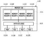
도 2는 도 1의 반도체 메모리 장치(10)의 메모리 미디어(100)에 포함되는 메모리 다이(110) 구성의 일 예를 나타내 보인 블록도이다. 즉, 본 예에 따른 메모리 다이(110)의 구성은, 도 1의 메모리 미디어(100)를 구성하는 n개의 메모리 다이들(110-1, …, 110-n) 각각에 대해 동일하게 적용될 수 있다. 도 2에서 메모리 다이(110) 내에 배치되는 모드 레지스터 세팅(MRS)의 도시는 생략되었다. 도 2를 참조하면, 메모리 다이(110)는, 메모리 저장영역(111)과 복수개의 데이터 입/출력 핀들(DQ0, DQ1, DQ2, DQ3)(112A, 112B, 112C, 112D)을 포함한다. 메모리 저장영역(111)은, 복수개, 예컨대 4개의 메모리 영역들(111A, 111B, 111C, 111D)로 구분될 수 있다. 메모리 다이(110)는, 메모리 영역들(111A, 111B, 111C, 111D) 각각과 데이터 입/출력 핀들(112A, 112B, 112C, 112D) 각각 사이의 데이터 입/출력을 인터페이싱하는 데이터 입/출력 로직(113)을 포함할 수 있다. 메모리 영역들(111A, 111B, 111C, 111D)의 개수는 데이터 입/출력 핀들(112A, 112B, 112C, 112D)의 개수와 동일하다.FIG. 2 is a block diagram showing an example of a configuration of a memory die 110 included in the
본 예에서 메모리 영역들(111A, 111B, 111C, 111D)의 구분은, 메모리 미디어(110) 외부와의 데이터 전송이 어떤 데이터 입/출력 핀을 통해 이루어지는지에 따라 이루어진다. 일 예에서, 첫번째 메모리 영역(memory region 0)(111A)은 첫번째 데이터 입/출력 핀(DQ0)(112A)을 통해 데이터 입/출력이 이루어지는 영역으로 한정될 수 있다. 두번째 메모리 영역(memory region 1)(111B)은 두번째 데이터 입/출력 핀(DQ1)(112B)을 통해 데이터 입/출력이 이루어지는 영역으로 한정될 수 있다. 세번째 메모리 영역(memory region 2)(111C)은 세번째 데이터 입/출력 핀(DQ2)(112C)을 통해 데이터 입/출력이 이루어지는 영역으로 한정될 수 있다. 네번째 메모리 영역(memory region 3)(111D)은 네번째 데이터 입/출력 핀(DQ3)(112D)을 통해 데이터 입/출력이 이루어지는 영역으로 한정될 수 있다.In this example, the
도 3은 도 1의 반도체 메모리 장치(10)의 메모리 미디어(100)에 포함되는 스페어 다이(120) 구성의 일 예를 나타내 보인 블록도이다. 즉, 본 예에 따른 스페어 다이(120)의 구성은, 도 1의 메모리 미디어(100)를 구성하는 m개의 스페어 다이들(120-1, …, 120-m) 각각에 대해 동일하게 적용될 수 있다. 도 3에서 스페어 다이(120) 내에 배치되는 모드 레지스터 세팅(MRS)의 도시는 생략되었다. 도 3을 참조하면, 스페어 다이(120)는, 스페어 저장영역(121)과 복수개의 데이터 입/출력 핀들(DQ0, DQ1, DQ2, DQ3)(122A, 122B, 122C, 122D)을 포함한다. 스페어 저장영역(121)은, 메모리 다이(도 2의 110)의 메모리 저장영역(111)과 동일하게 구성된다. 스페어 저장영역(121)은, 복수개, 예컨대 4개의 스페어 영역들(121A, 121B, 121C, 121D)로 구분될 수 있다. 스페어 다이(120)는, 스페어 영역들(121A, 121B, 121C, 121D) 각각과 데이터 입/출력 핀들(122A, 122B, 122C, 122D) 각각 사이의 데이터 입/출력을 인터페이싱하는 데이터 입/출력 로직(123)을 포함할 수 있다. 스페어 영역들(121A, 121B, 121C, 121D)의 개수는 데이터 입/출력 핀들(122A, 122B, 122C, 122D)의 개수와 동일하다.FIG. 3 is a block diagram showing an example of a configuration of a
본 예에서 스페어 영역들(121A, 121B, 121C, 121D)의 구분은, 메모리 미디어(110) 외부와의 데이터 전송이 어떤 데이터 입/출력 핀을 통해 이루어지는지에 따라 이루어진다. 일 예에서, 첫번째 스페어 영역(spare region 0)(121A)은 첫번째 데이터 입/출력 핀(DQ0)(122A)을 통해 데이터 입/출력이 이루어지는 영역으로 한정될 수 있다. 두번째 스페어 영역(spare region 1)(121B)은 두번째 데이터 입/출력 핀(DQ1)(122B)을 통해 데이터 입/출력이 이루어지는 영역으로 한정될 수 있다. 세번째 스페어 영역(spare region 2)(111C)은 세번째 데이터 입/출력 핀(DQ2)(122C)을 통해 데이터 입/출력이 이루어지는 영역으로 한정될 수 있다. 네번째 스페어 영역(spare region 3)(121D)은 네번째 데이터 입/출력 핀(DQ3)(122D)을 통해 데이터 입/출력이 이루어지는 영역으로 한정될 수 있다. 스페어 다이(120)의 첫번째 스페어 영역(spare region 0)(121A), 두번째 스페어 영역(spare region 1)(121B), 세번째 스페어 영역(spare region 2)(121C), 및 네번째 스페어 영역(spare region 3)(121D)은, 각각 메모리 다이(도 2의 110)의 첫번째 메모리 영역(memory region 0)(111A), 두번째 메모리 영역(memory region 1)(111B), 세번째 메모리 영역(memory region 2)(111C), 및 네번째 메모리 영역(memory region 3)(111D)과 동일하게 구성된다.In this example, the
도 4 및 도 5는 본 개시에 따른 반도체 메모리 장치(10)의 데이터 입/출력 핀 단위로의 리페어 방법의 일 예를 설명하기 위해 나타내 보인 도면이다. 본 예에서 3개의 메모리 다이들(110-1, 110-2, 110-3)과 1개의 스페어 다이(120)를 갖는 메모리 미디어의 경우를 예로 들기로 한다. 본 예에서 메모리 다이들(110-1, 110-2, 110-3) 각각은 4개의 데이터 입/출력 핀들(DQ0, DQ1, DQ2, DQ3)을 갖는다. 메모리 다이들(110-1, 110-2, 110-3) 각각은, 도 2를 참조하여 설명한 메모리 다이(110)와 동일한 구성을 갖는다. 또한 스페어 다이(120)는, 도 3을 참조하여 설명한 스페어 다이(120)와 동일한 구성을 갖는다.4 and 5 are diagrams shown to explain an example of a repair method in units of data input/output pins of the
도 4를 참조하면, 메모리 다이들(110-1, 110-2, 110-3) 각각에 대한 데이터 액세스 과정에서, 데이터 입/출력 핀 리페어 제어 회로(230)에 의해 첫번째 메모리 다이(memory die 0)(110-1)의 데이터 입/출력 핀들 중 네번째 데이터 입/출력 핀(DQ3)이 고장인 것으로 판정되는 경우, 고장난 네번째 데이터 입/출력 핀(DQ3)은 스페어 다이(spare die)(120)의 첫번째 데이터 입/출력 핀(DQ0)으로 대체되는 데이터 입/출력 핀 단위로의 리페어가 수행된다. 즉 고장난 네번째 데이터 입/출력 핀(DQ3)을 갖는 첫번째 메모리 다이(110-1)의 나머지 데이터 입/출력 핀들(DQ0, DQ1, DQ2)은 리페어 과정에 의해 영향을 받지 않는다. 이 리페어 과정이 수행되면, 첫번째 메모리 다이(110-1)의 네번째 데이터 입/출력 핀(DQ3)을 통해 데이터 액세스가 이루어지는 대신에 스페어 다이(120)의 첫번째 데이터 입/출력 핀(DQ0)을 통해 데이터 액세스가 이루어진다.Referring to FIG. 4 , in a data access process for each of the memory dies 110-1, 110-2, and 110-3, the first memory die (memory die 0) is controlled by the data input/output pin repair control circuit 230. ) (110-1), when it is determined that the fourth data input/output pin (DQ3) is defective, the failed fourth data input/output pin (DQ3) is a spare die (120). Repair is performed in units of data input/output pins replaced with the first data input/output pin (DQ0) of . That is, the remaining data I/O pins DQ0 , DQ1 , and DQ2 of the first memory die 110 - 1 having the fourth data I/O pin DQ3 that is broken are not affected by the repair process. When this repair process is performed, data access is performed through the first data input/output pin DQ0 of the
도 5를 참조하면, 첫번째 메모리 다이(110-1)의 네번째 데이터 입/출력 핀(DQ3)이 스페어 다이(120)의 첫번째 데이터 입/출력 핀(DQ0)으로 대체되는 리페어가 수행된 상태에서, 데이터 입/출력 핀 리페어 제어 회로(230)에 의해 세번째 메모리 다이(memory die 2)(110-3)의 데이터 입/출력 핀들 중 두번째 데이터 입/출력 핀(DQ1)이 고장인 것으로 판정되는 경우를 예로 들기로 한다. 이 경우 고장난 두번째 데이터 입/출력 핀(DQ1)은 스페어 다이(spare die)(120)의 남아있는 데이터 입/출력 핀들 중 하나, 예컨대 두번째 데이터 입/출력 핀(DQ1)으로 대체되는 데이터 입/출력 핀 단위로의 리페어가 수행된다. 즉 고장난 두번째 데이터 입/출력 핀(DQ1)을 갖는 세번째 메모리 다이(110-3)의 나머지 데이터 입/출력 핀들(DQ0, DQ2, DQ3)은 리페어 과정에 의해 영향을 받지 않는다. 이 리페어 과정이 수행되면, 세번째 메모리 다이(110-3)의 두번째 데이터 입/출력 핀(DQ1)을 통해 데이터 액세스가 이루어지는 대신에 스페어 다이(120)의 두번째 데이터 입/출력 핀(DQ1)을 통해 데이터 액세스가 이루어진다.Referring to FIG. 5 , in a state in which repair is performed in which the fourth data input/output pin DQ3 of the first memory die 110-1 is replaced with the first data input/output pin DQ0 of the
데이터 입/출력 핀 단위로의 리페어가 수행되면, 고장난 데이터 입/출력 핀을 통한 데이터 액세스는 중지되며, 고장난 데이터 입/출력 핀을 대체하는 스페어 다이의 데이터 입/출력 핀을 통한 데이터 액세스가 이루어진다. 이를 위해서는, 메모리 다이의 고장난 데이터 입/출력 핀을 통해 입/출력되던 데이터가 스페어 다이의 대체된 데이터 입/출력 핀을 통해 입/출력되도록 메모리 다이로부터 스페어 다이로의 데이터 이주(data migration)를 수행하여야 한다. 메모리 다이에 저장된 데이터는 ECC 인코딩에 의해 형성된 코드워드 형태를 가지므로, 데이터 이주 과정을 수행하기 위해서는 ECC 회로(220)를 통한 ECC 디코딩 및 ECC 인코딩을 다시 수행할 필요가 있다.When repair is performed in units of data I/O pins, data access through the failed data I/O pin is stopped, and data access is made through the data I/O pin of the spare die replacing the failed data I/O pin. . To this end, data migration from the memory die to the spare die is performed so that the data input/output through the failed data I/O pin of the memory die is input/output through the replaced data I/O pin of the spare die. should be performed Since the data stored in the memory die has a codeword form formed by ECC encoding, it is necessary to perform ECC decoding and ECC encoding again through the
도 6은 본 개시에 따른 반도체 메모리 장치(10)의 데이터 입/출력 핀 단위로의 리페어 방법을 설명하기 위해 나타내 보인 플로챠트이다. 그리고 도 7은 본 개시에 따른 반도체 메모리 장치(10)의 데이터 입/출력 핀 단위로의 리페어 방법에서 모드 레지스터 세팅의 설정 과정을 설명하기 위해 나타내 보인 도면이다. 또한 도 8 및 도 9는 본 개시에 따른 반도체 메모리 장치(10)의 데이터 입/출력 핀 단위로의 리페어 방법에서 데이터 이주 과정을 설명하기 위해 나타내 보인 도면들이다. 도 6 을 참조하면, 먼저 스페어 다이(120)의 모드 레지스터 세팅(MRS)의 설정값을 변경하여 스페어 다이(120)의 첫번째 데이터 입/출력 핀(DQ0)을 활성화시킨다(단계 310). 이와 같은 과정을 통해 스페어 다이(120)의 첫번째 데이터 입/출력 핀(DQ0)을 통해 스페어 다이(120) 내의 저장영역으로 데이터를 저장할 수 있게 된다.6 is a flow chart shown to explain a repair method in units of data input/output pins of the
도 7에 나타낸 바와 같이, 모드 레지스터 세팅(MRS)은, 데이터 입/출력 핀들의 활성화 또는 비활성화를 설정할 수 있는 4 비트의 코드를 갖는다. 스페어 다이(120)가 갖는 모드 레지스터 세팅(MRS)과, 메모리 다이들(110-1, 110-2, 110-3) 각각이 갖는 모드 레지스터 세팅(MRS)은 동일하게 구성된다. 4 비트의 코드를 구성하는 바이너리(binary) 값들 중 첫번째 비트값(A0)은 첫번째 데이터 입/출력 핀(DQ0)의 활성화 또는 비활성화를 설정한다. 첫번째 비트값(A0)이 "0"인 경우 첫번째 데이터 입/출력 핀(DQ0)은 비활성화되고, "1"인 경우에는 활성화된다. 4 비트의 코드를 구성하는 바이너리 값들 중 두번째 비트값(A1)은 두번째 데이터 입/출력 핀(DQ1)의 활성화 또는 비활성화를 설정한다. 두번째 비트값(A1)이 "0"인 경우 두번째 데이터 입/출력 핀(DQ1)은 비활성화되고, "1"인 경우에는 활성화된다. 4 비트의 코드를 구성하는 바이너리 값들 중 세번째 비트값(A2)은 세번째 데이터 입/출력 핀(DQ2)의 활성화 또는 비활성화를 설정한다. 세번째 비트값(A2)이 "0"인 경우 세번째 데이터 입/출력 핀(DQ2)은 비활성화되고, "1"인 경우에는 활성화된다. 4 비트의 코드를 구성하는 바이너리 값들 중 네번째 비트값(A3)은 네번째 데이터 입/출력 핀(DQ3)의 활성화 또는 비활성화를 설정한다. 네번째 비트값(A3)이 "0"인 경우 네번째 데이터 입/출력 핀(DQ3)은 비활성화되고, "1"인 경우에는 활성화된다.As shown in Figure 7, the mode register setting (MRS) has a 4-bit code that can set the activation or deactivation of data input/output pins. The mode register setting (MRS) of the
스페어 다이(120)의 모드 레지스터 세팅(MRS)은, 스페어 다이(120)로의 리페어가 수행되기 전까지 모든 데이터 입/출력 핀들(DQ0-DQ3)이 비활성화되도록 설정된다. 즉 스페어 다이(120)의 모드 레지스터 세팅(MRS)의 4 비트의 코드를 구성하는 바이너리 값들은 모두 "0"의 값으로 설정되어 있다. 따라서 데이터 입/출력 단위로의 리페어를 위한 데이터 이주 과정을 수행하기 위해서는, 먼저 스페어 다이(120)의 모드 레지스터 세팅(MRS)의 4 비트의 코드를 구성하는 바이너리 값들 중 첫번째 비트값(A0)을 "0"에서 "1"로 변경하여, 첫번째 데이터 입/출력 핀(DQ0)이 활성화되도록 한다. 스페어 다이(120)의 모드 레지스터 세팅(MRS)의 설정값 변경을 통해, 첫번째 데이터 입/출력 핀(DQ0)을 통한 데이터 전송이 가능해지면, 메모리 다이로부터 스페어 다이로의 데이터 이주 동작이 수행된다.The mode register setting (MRS) of the
도 8에 나타낸 바와 같이, 데이터 입/출력 핀 단위로의 리페어를 수행하는 과정에서 데이터 이주는, 첫번째 메모리 다이(memory die 0)(110-1)의 고장난 네번째 데이터 입/출력 핀(DQ4)을 통해 데이터가 전송되는 네번째 메모리 영역(memory region 3)(111-1D)의 데이터를 스페어 다이(spare die)(120)의 첫번째 데이터 입/출력 핀(DQ0)을 통해 데이터가 전송되는 첫번째 스페어 영역(spare region 0)(121A)으로 이주(migration)시킴으로써 수행될 수 있다. 네번째 메모리 영역(memory region 3)(111-1D)에 저장된 데이터는 ECC 동작의 단위인 심볼들로 구성될 수 있다. 이 경우 네번째 메모리 영역(111-1D)에 저장된 심볼들 중 일부는 첫번째 메모리 다이(memory die 0)(110-1)의 다른 메모리 영역들(111-1A, 111-1B, 111-1C) 내에 저장된 심볼들과 함께 ECC 인코딩이 수행되는 경우가 발생될 수 있다. 따라서 데이터 이주시, 첫번째 메모리 다이(memory die 0)(110-1) 내의 모든 메모리 영역들(111-1A, …, 111-1D)에 저장된 전체 데이터에 대해 ECC 디코딩을 수행한다. 그리고 ECC 디코딩된 데이터에 대해 ECC 인코딩을 수행한 후에 데이터를 이주시킨다. 이를 위해 먼저 어드레스를 "0"으로 설정한다(단계 320). 여기서 "어드레스=0"은 고장난 네번째 데이터 입/출력 핀(DQ3)을 갖는 첫번째 메모리 다이(110-1) 내의 메모리 저장영역의 첫번째 어드레스를 의미한다.As shown in FIG. 8, data migration in the process of performing repair in units of data input/output pins removes the failed fourth data input/output pin DQ4 of the first memory die 0 (110-1). The data of the fourth memory region (memory region 3) (111-1D) to which data is transmitted through the first spare region (to which data is transmitted) through the first data input / output pin (DQ0) of the spare die (120) It can be performed by migrating to spare region 0) (121A). Data stored in the fourth memory region (memory region 3) 111-1D may be composed of symbols that are units of ECC operation. In this case, some of the symbols stored in the fourth memory area 111-1D are stored in other memory areas 111-1A, 111-1B, and 111-1C of the first memory die 0 (110-1). A case in which ECC encoding is performed with symbols may occur. Accordingly, during data migration, ECC decoding is performed on all data stored in all memory areas 111-1A, ..., 111-1D in the first memory die 0 110-1. After performing ECC encoding on the ECC decoded data, the data is migrated. To this end, the address is first set to "0" (step 320). Here, "address=0" means the first address of the memory storage area in the first memory die 110-1 having the failed fourth data input/output pin DQ3.
첫번째 메모리 다이(memory die 0)(110-1)의 어드레스 "0"을 갖는 데이터를 읽은 후에 ECC 디코딩을 수행한다(단계 330). 이 과정을 통해 코드워드 형태의 리드 데이터는 패리티 비트가 제거된 원래의 리드 데이터가 되고, 에러가 발생되는 경우 에러정정능력 범위 내에서 에러는 정정된다. ECC 디코딩이 수행되면, 첫번째 메모리 다이(110-1)의 고장난 네번째 데이터 입/출력 핀(DQ3)을 스페어 다이(120)의 활성화된 첫번째 데이터 입/출력 핀(DQ0)으로 할당하는 아비트레이션(arbitration)을 수행한다(단계 340). 다음에 ECC 디코딩된 데이터에 대해 ECC 인코딩을 수행하고, ECC 인코딩된 데이터를 스페어 다이(120)에 라이트한다(단계 350). 이때 ECC 인코딩은, 첫번째 메모리 다이(111-1)의 메모리 영역들(111-1A, …, 111-1D) 각각에 저장된 데이터 별로 구분하여 수행한다. 즉 첫번째 메모리 영역(111-1A)에 저장된 데이터에 대한 ECC 인코딩과, 두번째 메모리 영역(111-1B)에 저장된 데이터에 대한 ECC 인코딩과, 세번째 메모리 영역(111-1C)에 저장된 데이터에 대한 ECC 인코딩과, 그리고 네번째 메모리 영역(111-1D)에 저장된 데이터에 대한 ECC 인코딩을 각각 수행한다.ECC decoding is performed after reading data having address “0” of the first memory die 0 110-1 (step 330). Through this process, read data in the form of a codeword becomes original read data from which parity bits are removed, and if an error occurs, the error is corrected within the error correction capability range. When ECC decoding is performed, an arbitration for allocating the failed fourth data input/output pin DQ3 of the first memory die 110-1 to the activated first data input/output pin DQ0 of the spare die 120 ) is performed (step 340). Next, ECC encoding is performed on the ECC decoded data, and the ECC encoded data is written to the spare die 120 (step 350). At this time, ECC encoding is performed separately for each data stored in each of the memory areas 111-1A, ..., 111-1D of the first memory die 111-1. That is, ECC encoding for data stored in the first memory area 111-1A, ECC encoding for data stored in the second memory area 111-1B, and ECC encoding for data stored in the third memory area 111-1C. ECC encoding is performed on data stored in and the fourth memory area 111-1D, respectively.
ECC 인코딩이 수행된 후에는, 네번째 메모리 영역(111-1D)에 저장된 데이터를 제외한 나머지 데이터를 첫번째 메모리 영역(111-1A), 두번째 메모리 영역(111-1B), 및 세번째 메모리 영역(111-1C)에 각각 라이트한다. 이에 따라 첫번째 메모리 영역(111-1A)에 라이트된 데이터는 첫번째 메모리 다이(110-1)의 첫번째 데이터 입/출력 핀(DQ0)을 통해 액세스된다. 두번째 메모리 영역(111-1B)에 라이트된 데이터는 첫번째 메모리 다이(110-1)의 두번째 데이터 입/출력 핀(DQ1)을 통해 액세스된다. 세번째 메모리 영역(111-1C)에 라이트된 데이터는 첫번째 메모리 다이(110-1)의 세번째 데이터 입/출력 핀(DQ2)을 통해 액세스된다. 그리고 네번째 메모리 영역(111-1D)에 저장된 데이터는 스페어 다이(120)의 첫번째 스페어 영역(spare region 0)(121A)에 라이트한다. 스페어 다이(120)의 첫번째 스페어 영역(121A)에 라이트된 데이터는 스페어 다이(120)의 첫번째 데이터 입/출력 핀(DQ0)을 통해 액세스된다.After ECC encoding is performed, data other than the data stored in the fourth memory area 111-1D is transferred to the first memory area 111-1A, the second memory area 111-1B, and the third memory area 111-1C. ), respectively. Accordingly, data written in the first memory area 111-1A is accessed through the first data input/output pin DQ0 of the first memory die 110-1. Data written to the second memory area 111-1B is accessed through the second data input/output pin DQ1 of the first memory die 110-1. Data written to the third memory area 111-1C is accessed through the third data input/output pin DQ2 of the first memory die 110-1. Data stored in the fourth memory region 111-1D is written to the first spare region 0 (121A) of the
어드레스 "0"을 갖는 데이터에 대해 단계 350에서의 ECC 인코딩 및 데이터 쓰기 단계가 수행된 후에는 현재의 어드레스가 마지막 어드레스인지의 여부를 판단한다(단계 360). 단계 360에서의 판단 결과, 현재의 어드레스 "0"이 마지막 어드레스가 아닌 경우, 어드레스를 증가시킨다(단계 370). 즉 "어드레스+1"로 어드레스를 변경시킨다. 그리고 어드레스 "1"을 갖는 데이터에 대해 단계 330 내지 단계 350을 다시 수행한다. 단계 360에서의 판단 결과, 현재의 어드레스가 마지막 어드레스인 경우, 고장난 네번째 데이터 입/출력 핀(DQ3)을 갖는 첫번째 메모리 다이(110-1)의 모드 레지스터 세팅(MRS)을 설정해서 첫번째 메모리 다이(110-1)의 고장난 네번째 데이터 입/출력 핀(DQ3)을 비활성화시킨다(단계 380). 도 7을 참조하여 설명한 바와 유사하게, 첫번째 메모리 다이(110-1)의 모드 레지스터 세팅(MRS)(114-1)의 4 비트의 코드를 구성하는 바이너리 값들 중 네번째 비트값(A3)을 "1"에서 "0"로 변경하여, 네번째 데이터 입/출력 핀(DQ3)이 비활성화되도록 한다. 이와 같은 첫번째 메모리 다이(110-1)의 모드 레지스터 세팅(MRS)(114-1)의 설정값 변경을 통해, 네번째 데이터 입/출력 핀(DQ3)을 통한 데이터 액세스가 차단된다.After the ECC encoding and data writing steps in
도 5를 참조하여 설명한 바와 같이, 스페어 다이(120)의 첫번째 데이터 입/출력 핀(DQ0)이 이전의 데이터 입/출력 핀 단위로의 리페어에 의해 사용된 상태에서, 데이터 입/출력 핀 리페어 제어 회로(230)에 의해 세번째 메모리 다이(110-3)의 데이터 입/출력 핀들 중 두번째 데이터 입/출력 핀(DQ1)이 고장인 것으로 판정되면, 다시 데이터 입/출력 핀 단위로의 리페어 동작이 수행된다. 이 경우 세번째 메모리 다이(110-3)의 고장난 두번째 데이터 입/출력 핀(DQ1)은 스페어 다이(120)의 남아있는 데이터 입/출력 핀들 중 하나, 예컨대 두번째 데이터 입/출력 핀(DQ1)으로 대체될 수 있다. 구체적으로 먼저 스페어 다이(120)의 모드 레지스터 세팅(MRS)의 설정값을 변경하여 스페어 다이(120)의 두번째 데이터 입/출력 핀(DQ1)을 활성화시킨다. 즉, 스페어 다이(120)의 모드 레지스터 세팅(MRS)(124)의 4 비트의 코드를 구성하는 바이너리 값들 중 두번째 비트값(A1)을 "0"에서 "1"로 변경하여, 두번째 데이터 입/출력 핀(DQ1)이 활성화되도록 한다.As described with reference to FIG. 5 , in a state in which the first data input/output pin DQ0 of the
도 9에 나타낸 바와 같이, 데이터 입/출력 핀 단위로의 리페어를 수행하는 과정에서 데이터 이주는, 세번째 메모리 다이(memory die 2)(110-3)의 고장난 두번째 데이터 입/출력 핀(DQ1)을 통해 데이터가 전송되는 두번째 메모리 영역(111-3B)의 데이터를 스페어 다이(spare die)(120)의 두번째 데이터 입/출력 핀(DQ1)을 통해 데이터가 전송되는 두번째 스페어 영역(121B)으로 이주시킴으로써 수행될 수 있다. 이 경우 데이터 이주는 도 8을 참조하여 설명한 바와 동일한 과정으로 수행된다. 즉 세번째 메모리 다이(110-3) 내의 모든 메모리 영역들(111-3A, …, 111-3D)에 저장된 전체 데이터에 대해 어드레스를 증가시키면서 ECC 디코딩을 수행한다. 그리고 ECC 디코딩된 데이터에 대해 ECC 인코딩을 수행한다. ECC 인코딩은 세번째 메모리 다이(110-3)의 메모리 영역들(111-3A, …, 111-3D) 각각에 대해 수행되도록 한다. ECC 디코딩이 수행되면, 세번째 메모리 다이(110-3)의 고장난 두번째 데이터 입/출력 핀(DQ1)을 스페어 다이(120)의 활성화된 두번째 데이터 입/출력 핀(DQ1)으로 할당하는 아비트레이션을 수행한다. 다음에 ECC 디코딩된 데이터에 대해 ECC 인코딩을 수행하고, ECC 인코딩된 데이터를 스페어 다이(120)에 라이트한다. 이에 따라 세번째 메모리 다이(110-3)의 두번째 메모리 영역(111-1B)에 저장된 데이터는 스페어 다이(120)의 두번째 스페어 영역(121B)에 라이트 된다. 모든 어드레스에 대해 데이터 이주 과정이 완료되면, 세번째 메모리 다이(110-3)의 모드 레지스터 세팅(MRS)(114-3)의 4 비트의 코드를 구성하는 바이너리 값들 중 두번째 비트값(A1)을 "1"에서 "0"로 변경하여, 고장난 두번째 데이터 입/출력 핀(DQ1)이 비활성화되도록 한다.As shown in FIG. 9, data migration in the process of performing repair in units of data input/output pins removes the failed second data input/output pin DQ1 of the third memory die 2 (110-3). By migrating the data of the second memory area 111-3B through which data is transmitted to the second
상술한 바와 같이 본 출원의 실시 형태들을 도면들을 예시하며 설명하지만, 이는 본 출원에서 제시하고자 하는 바를 설명하기 위한 것이며, 세밀하게 제시된 형상으로 본 출원에서 제시하고자 하는 바를 한정하고자 한 것은 아니다.As described above, the embodiments of the present application are exemplified and described, but this is for explaining what is intended to be presented in the present application, and is not intended to limit what is intended to be presented in the present application in a detailed form.
10...반도체 메모리 장치100...메모리 미디어
110-1, …, 110-n...메모리 다이120...스페어 다이
200...메모리 컨트롤러210...호스트 커맨드 프로세싱 회로
220...ECC 회로230...데이터 입/출력 리페어 제어 회로10 ...
110-1, … , 110-n...memory die 120...spare die
200 ...
220...
Claims (20)
Translated fromKorean상기 메모리 다이들 중 제1 메모리 다이의 데이터 입/출력 핀들 중 고장난 데이터 입/출력 핀을 상기 스페어 다이의 데이터 입/출력 핀들 중 어느 하나인 제1 데이터 입/출력 핀으로 대체하는 제1 리페어를 수행하는 데이터 입/출력 핀 리페어 제어 회로를 포함하되,
상기 데이터 입/출력 핀 리페어 제어 회로는, 상기 제1 리페어를 수행한 후, 상기 메모리 다이들 중 제2 메모리 다이의 데이터 입/출력 핀들 중 고장난 데이터 입/출력 핀을 상기 스페어 다이의 데이터 입/출력 핀들 중 상기 제1 데이터 입/출력 핀과 다른 제2 데이터 입/출력 핀으로 대체하는 제2 리페어를 수행하는 반도체 메모리 장치.a memory medium including memory dies each having a plurality of memory areas and data input/output pins and a spare die having a plurality of spare areas and data input/output pins; and
A first repair of replacing a failed data input/output pin among data input/output pins of a first memory die among the memory dies with a first data input/output pin that is one of data input/output pins of the spare die; Including a data input / output pin repair control circuit that performs,
The data input/output pin repair control circuit, after performing the first repair, connects a failed data input/output pin among data input/output pins of a second memory die among the memory dies to a data input/output pin of the spare die. A semiconductor memory device performing a second repair of replacing output pins with second data input/output pins different from the first data input/output pins.
상기 메모리 다이들 각각의 메모리 영역들 각각은 상기 메모리 다이의 상기 데이터 입/출력 핀들 각각을 통해 데이터 입/출력이 이루어지는 영역이고, 그리고
상기 스페어 다이의 스페어 영역들 각각은 상기 스페어 다이의 상기 데이터 입/출력 핀들 각각을 통해 데이터 입/출력이 이루어지는 영역인 반도체 메모리 장치.According to claim 1,
Each of the memory areas of each of the memory dies is an area in which data input/output is performed through each of the data input/output pins of the memory die, and
Each of the spare areas of the spare die is an area in which data input/output is performed through each of the data input/output pins of the spare die.
상기 메모리 다이들에 대한 리드 및 라이트 과정에서 에러정정코드(ECC) 동작을 수행하는 ECC 회로를 더 포함하는 반도체 메모리 장치.According to claim 1,
The semiconductor memory device further comprising an ECC circuit performing an error correction code (ECC) operation during read and write processes of the memory dies.
상기 데이터 입/출력 핀 리페어 제어 회로는, 메모리 다이의 메모리 영역들 중 상기 고장난 데이터 입/출력 핀을 통해 데이터 입/출력이 수행되는 메모리 영역의 데이터를 상기 스페어 다이의 데이터 입/출력 핀들 중 리페어에 사용된 데이터 입/출력 핀을 통해 데이터 입/출력이 수행되는 스페어 영역으로 이주시키는 데이터 이주 동작을 제어하는 반도체 메모리 장치.According to claim 3,
The data input/output pin repair control circuit repairs data in a memory area where data input/output is performed through the failed data input/output pin among memory areas of the memory die among data input/output pins of the spare die. A semiconductor memory device that controls a data migration operation of migrating to a spare area where data input/output is performed through data input/output pins used in the semiconductor memory device.
상기 메모리 다이의 메모리 영역들의 데이터에 대해 어드레스를 증가하면서 ECC 디코딩이 수행되도록 하고,
상기 ECC 디코딩된 데이터에 대해 ECC 인코딩이 수행되도록 하며, 그리고
상기 ECC 인코딩된 데이터 일부를 상기 스페어 다이의 데이터 입/출력 핀들 중 리페어에 사용된 데이터 입/출력 핀을 통해 데이터 입/출력이 수행되는 스페어 영역에 라이트 하여 상기 데이터 이주 동작을 제어하는 반도체 메모리 장치.The method of claim 4, wherein the data input / output pin repair control circuit,
ECC decoding is performed while increasing an address for data in memory areas of the memory die;
ECC encoding is performed on the ECC decoded data, and
A semiconductor memory device that controls the data migration operation by writing some of the ECC-encoded data to a spare area where data input/output is performed through a data input/output pin used for repair among data input/output pins of the spare die. .
상기 고장난 데이터 입/출력 핀을 갖는 메모리 다이의 메모리 영역들 각각에 저장된 데이터 별로 구분하여 상기 ECC 인코딩이 수행되도록 제어하는 반도체 메모리 장치.The method of claim 5, wherein the data input / output pin repair control circuit,
The semiconductor memory device controlling the ECC encoding to be performed according to data stored in each of the memory regions of the memory die having the failed data input/output pin.
상기 리페어에 사용된 데이터 입/출력 핀을 통해 데이터 입/출력이 수행되는 스페어 영역에 라이트 되는 데이터는, 상기 고장난 데이터 입/출력 핀을 갖는 메모리 다이의 메모리 영역들 중 상기 고장난 데이터 입/출력 핀을 통해 데이터 입/출력이 이루어지는 메모리 영역의 데이터에 대해 ECC 인코딩된 데이터로 한정하는 반도 체 메모리 장치.The method of claim 6, wherein the data input / output pin repair control circuit,
Data written to the spare area where data input/output is performed through the data input/output pin used for the repair is stored on the failed data input/output pin among memory areas of the memory die having the failed data input/output pin. A semiconductor memory device that limits data in a memory area where data input/output is performed through ECC-encoded data.
상기 복수개의 메모리 다이들 각각 및 스페어 다이는, 각각의 데이터 입/출력 핀들 각각의 활성화 여부가 세팅되는 모드 레지스터 세팅을 포함하는 반도체 메모리 장치.According to claim 5,
The semiconductor memory device of claim 1 , wherein each of the plurality of memory dies and the spare die includes a mode register setting configured to set whether each data input/output pin is activated.
상기 고장난 데이터 입/출력 핀이 비활성화되도록 상기 고장난 데이터 입/출력 핀을 갖는 메모리 다이의 모드 레지스터 세팅을 설정하고, 그리고
리페어에 사용된 상기 스페어 다이의 데이터 입/출력 핀이 활성화되도록 상기 스페어 다이의 모드 레지스터 세팅을 설정하는 반도체 메모리 장치.The method of claim 8, wherein the data input / output pin repair control circuit,
set a mode register setting of a memory die having the failed data input/output pin such that the failed data input/output pin is disabled; and
A semiconductor memory device configured to set a mode register setting of the spare die so that a data input/output pin of the spare die used for repair is activated.
상기 고장난 데이터 입/출력 핀을 갖는 메모리 다이의 모드 레지스터 세팅을 설정하는 동작은 상기 데이터 이주 동작이 완료된 후에 수행되도록 하고, 그리고
상기 리페어에 사용된 상기 스페어 다이의 데이터 입/출력 핀이 활성화되도록 상기 스페어 다이의 모드 레지스터 세팅을 설정하는 동작은 상기 데이터 이주 동작이 시작되기 전에 수행되도록 하는 반도체 메모리 장치.The method of claim 9, wherein the data input / output pin repair control circuit,
setting the mode register setting of the memory die having the failed data input/output pin to be performed after the data migration operation is completed; and
The semiconductor memory device of claim 1 , wherein an operation of setting a mode register setting of the spare die so that a data input/output pin of the spare die used for the repair is activated is performed before the data migration operation starts.
상기 데이터 입/출력 핀 리페어 제어 회로는, 상기 리페어를 수행하기 전에 호스트로 상기 호스트의 메모리 액세스 동작을 중단하는 할트 신호를 전송하는 반도체 메모리 장치.According to claim 1,
The semiconductor memory device of claim 1 , wherein the data input/output pin repair control circuit transmits a HALT signal for stopping a memory access operation of the host to a host before performing the repair.
상기 메모리 다이들 중 제1 메모리 다이의 데이터 입/출력 핀들 중 고장난 데이터 입/출력 핀을 상기 스페어 다이의 데이터 입/출력 핀들 중 어느 하나인 제1 데이터 입/출력 핀으로 대체하는 제1 리페어를 수행하는 단계; 및
상기 제1 리페어를 수행한 후, 상기 메모리 다이들 중 제2 메모리 다이의 데이터 입/출력 핀들 중 고장난 데이터 입/출력 핀을 상기 스페어 다이의 데이터 입/출력 핀들 중 상기 제1 데이터 입/출력 핀과 다른 제2 데이터 입/출력 핀으로 대체하는 제2 리페어를 수행하는 단계를 포함하는 반도체 메모리 장치의 리페어 방법.A repair method for a semiconductor memory device including memory dies each having a plurality of memory areas and data input/output pins and a spare die having a plurality of spare areas and data input/output pins, the method comprising:
A first repair of replacing a failed data input/output pin among data input/output pins of a first memory die among the memory dies with a first data input/output pin that is one of data input/output pins of the spare die; performing steps; and
After performing the first repair, the failed data input/output pin among the data input/output pins of the second memory die among the memory dies is replaced with the first data input/output pin among the data input/output pins of the spare die. A repair method of a semiconductor memory device, comprising performing a second repair in which a second data input/output pin is replaced with a different second data input/output pin.
상기 메모리 다이들 각각의 메모리 영역들 각각은 상기 메모리 다이의 상기 데이터 입/출력 핀들 각각을 통해 데이터 입/출력이 이루어지는 영역이고, 그리고
상기 스페어 다이의 스페어 영역들 각각은 상기 스페어 다이의 상기 데이터 입/출력 핀들 각각을 통해 데이터 입/출력이 이루어지는 영역인 반도체 메모리 장치의 리페어 방법.According to claim 12,
Each of the memory areas of each of the memory dies is an area in which data input/output is performed through each of the data input/output pins of the memory die, and
Each of the spare areas of the spare die is an area in which data input/output is performed through each of the data input/output pins of the spare die.
상기 고장난 데이터 입/출력 핀을 상기 스페어 다이의 데이터 입/출력 핀들 중 리페어에 사용되지 않은 데이터 입/출력 핀들 중 어느 하나에 아비트레이션시키는 단계; 및
상기 고장난 데이터 입/출력 핀을 통해 데이터 입/출력이 이루어지는 메모리 영역의 데이터를 상기 리페어에 사용된 데이터 입/출력 핀을 통해 데이터 입/출력이 이루어지는 스페어 영역으로 라이트 하는 데이터 이주 단계를 포함하는 반도체 메모리 장치의 리페어 방법.14. The method of claim 13, wherein the performing of the first repair and the performing of the second repair include:
arbitrating the failed data input/output pin to one of data input/output pins not used for repair among data input/output pins of the spare die; and
and a data migration step of writing data in a memory area where data is input/output through the failed data input/output pin to a spare area where data is input/output through the data input/output pin used for the repair. How to repair a memory device.
상기 스페어 다이의 데이터 입/출력 핀들 중 리페어에 아비트레이션된 데이터 입/출력 핀을 활성화시키는 단계를 더 포함하는 반도체 메모리 장치의 리페어 방법.According to claim 14,
The repair method of the semiconductor memory device further comprising activating a data input/output pin arbitrated for repair among data input/output pins of the spare die.
상기 리페어에 아비트레이션된 데이터 입/출력 핀을 활성화시키는 단계는 상기 데이터 이주 단계를 수행하기 전에 수행되도록 하는 반도체 메모리 장치의 리페어 방법.According to claim 15,
The repair method of the semiconductor memory device, wherein the activating the data input/output pins arbitrated for repair is performed before performing the data migration step.
어드레스를 증가시키면서 상기 고장난 데이터 입/출력 핀을 갖는 메모리 다이의 데이터를 읽어 에러정정코드(ECC) 디코딩을 수행하는 단계;
상기 ECC 디코딩된 데이터에 대해 상기 고장난 데이터 입/출력 핀을 갖는 메모리 다이의 메모리 영역들 별로 구분하여 ECC 인코딩을 수행하는 단계; 및
상기 고장난 데이터 입/출력 핀을 통해 데이터 입/출력이 이루어지는 메모리 영역의 상기 ECC 인코딩된 데이터를 상기 리페어에 사용된 데이터 입/출력 핀을 통해 데이터 입/출력이 이루어지는 스페어 영역으로 라이트 하는 단계를 포함하는 반도체 메모리 장치의 리페어 방법.15. The method of claim 14, wherein the data migration step,
performing error correction code (ECC) decoding by reading data of the memory die having the failed data input/output pin while increasing an address;
performing ECC encoding on the ECC decoded data according to memory areas of a memory die having the failed data input/output pin; and
and writing the ECC-encoded data of a memory area where data input/output is performed through the failed data input/output pin to a spare area where data input/output is performed through the data input/output pin used for the repair. A method for repairing a semiconductor memory device.
상기 고장난 데이터 입/출력 핀을 비활성화시키는 단계를 더 포함하는 반도체 메모리 장치의 리페어 방법.According to claim 14,
The repair method of the semiconductor memory device further comprising the step of inactivating the failed data input/output pin.
상기 고장난 데이터 입/출력 핀을 비활성화시키는 단계는 상기 데이터 이주 단계가 종료된 후에 수행되도록 하는 반도체 메모리 장치의 리페어 방법.According to claim 18,
The repair method of the semiconductor memory device, wherein the step of inactivating the failed data input/output pin is performed after the data migration step is finished.
상기 리페어를 수행하기 전에 호스트로 상기 호스트의 메모리 액세스 동작을 중단하는 할트 신호를 전송하는 단계를 더 포함하는 반도체 메모리 장치의 리페어 방법.According to claim 12,
The repair method of the semiconductor memory device further comprising transmitting a HALT signal for stopping a memory access operation of the host to a host before performing the repair.
Priority Applications (3)
| Application Number | Priority Date | Filing Date | Title |
|---|---|---|---|
| KR1020180038902AKR102483476B1 (en) | 2018-04-03 | 2018-04-03 | Semiconductor memory apparatus supporting repair with data I/O terminal as a unit and method of repairing the semiconductor memory apparatus |
| CN201811472205.4ACN110349613B (en) | 2018-04-03 | 2018-12-04 | Semiconductor memory system and method of repairing the same |
| US16/212,302US11036597B2 (en) | 2018-04-03 | 2018-12-06 | Semiconductor memory system and method of repairing the semiconductor memory system |
Applications Claiming Priority (1)
| Application Number | Priority Date | Filing Date | Title |
|---|---|---|---|
| KR1020180038902AKR102483476B1 (en) | 2018-04-03 | 2018-04-03 | Semiconductor memory apparatus supporting repair with data I/O terminal as a unit and method of repairing the semiconductor memory apparatus |
Publications (2)
| Publication Number | Publication Date |
|---|---|
| KR20190115788A KR20190115788A (en) | 2019-10-14 |
| KR102483476B1true KR102483476B1 (en) | 2023-01-03 |
Family
ID=68056272
Family Applications (1)
| Application Number | Title | Priority Date | Filing Date |
|---|---|---|---|
| KR1020180038902AActiveKR102483476B1 (en) | 2018-04-03 | 2018-04-03 | Semiconductor memory apparatus supporting repair with data I/O terminal as a unit and method of repairing the semiconductor memory apparatus |
Country Status (3)
| Country | Link |
|---|---|
| US (1) | US11036597B2 (en) |
| KR (1) | KR102483476B1 (en) |
| CN (1) | CN110349613B (en) |
Families Citing this family (6)
| Publication number | Priority date | Publication date | Assignee | Title |
|---|---|---|---|---|
| KR102813414B1 (en)* | 2019-01-24 | 2025-05-27 | 에스케이하이닉스 주식회사 | Memory system and operation method of memory system |
| US11281578B2 (en) | 2019-08-20 | 2022-03-22 | Micron Technology, Inc. | Garbage collection in a memory sub-system during a low battery state |
| US11282567B2 (en) | 2019-08-20 | 2022-03-22 | Micron Technology, Inc. | Sequential SLC read optimization |
| US11726869B2 (en)* | 2019-08-20 | 2023-08-15 | Micron Technology, Inc. | Performing error control operation on memory component for garbage collection |
| US11281392B2 (en) | 2019-08-28 | 2022-03-22 | Micron Technology, Inc. | Garbage collection in a memory component using an adjusted parameter |
| TWI731671B (en)* | 2020-05-07 | 2021-06-21 | 美商矽成積體電路股份有限公司 | Method and system for detecing abnormal dies |
Citations (5)
| Publication number | Priority date | Publication date | Assignee | Title |
|---|---|---|---|---|
| US20050030815A1 (en) | 2002-05-21 | 2005-02-10 | Mitsubishi Denki Kabushiki Kaisha | Semiconductor memory module |
| US20130326293A1 (en)* | 2012-05-31 | 2013-12-05 | Naveen Muralimanohar | Memory error test routine |
| US20130339820A1 (en) | 2012-06-14 | 2013-12-19 | International Business Machines Corporation | Three dimensional (3d) memory device sparing |
| US20150378801A1 (en)* | 2014-06-27 | 2015-12-31 | Sandisk Technologies Inc. | Systems and Methods for Fast Bit Error Rate Estimation |
| US20160299814A1 (en) | 2010-01-11 | 2016-10-13 | Apple Inc. | Redundant data storage schemes for multi-die memory systems |
Family Cites Families (10)
| Publication number | Priority date | Publication date | Assignee | Title |
|---|---|---|---|---|
| US5177744A (en)* | 1990-09-04 | 1993-01-05 | International Business Machines Corporation | Method and apparatus for error recovery in arrays |
| US5920513A (en)* | 1997-08-22 | 1999-07-06 | Micron Technology, Inc. | Partial replacement of partially defective memory devices |
| KR101377305B1 (en)* | 2005-06-24 | 2014-03-25 | 구글 인코포레이티드 | An integrated memory core and memory interface circuit |
| KR20110073932A (en)* | 2009-12-24 | 2011-06-30 | 주식회사 하이닉스반도체 | Semiconductor storage system including ECC circuit and control method thereof |
| KR101218606B1 (en) | 2011-02-28 | 2013-01-04 | 에스케이하이닉스 주식회사 | Semiconductor memory device |
| KR20140078283A (en)* | 2012-12-17 | 2014-06-25 | 에스케이하이닉스 주식회사 | Repair device |
| KR101862379B1 (en)* | 2013-04-19 | 2018-07-05 | 삼성전자주식회사 | Memory device with error correction code and redundancy repair operations |
| US10078567B2 (en)* | 2016-03-18 | 2018-09-18 | Alibaba Group Holding Limited | Implementing fault tolerance in computer system memory |
| KR20190012566A (en)* | 2017-07-27 | 2019-02-11 | 삼성전자주식회사 | Memory system having an error correction function and operating method of memory module and memory controller |
| US10802910B2 (en)* | 2018-09-17 | 2020-10-13 | Intel Corporation | System for identifying and correcting data errors |
- 2018
- 2018-04-03KRKR1020180038902Apatent/KR102483476B1/enactiveActive
- 2018-12-04CNCN201811472205.4Apatent/CN110349613B/enactiveActive
- 2018-12-06USUS16/212,302patent/US11036597B2/enactiveActive
Patent Citations (5)
| Publication number | Priority date | Publication date | Assignee | Title |
|---|---|---|---|---|
| US20050030815A1 (en) | 2002-05-21 | 2005-02-10 | Mitsubishi Denki Kabushiki Kaisha | Semiconductor memory module |
| US20160299814A1 (en) | 2010-01-11 | 2016-10-13 | Apple Inc. | Redundant data storage schemes for multi-die memory systems |
| US20130326293A1 (en)* | 2012-05-31 | 2013-12-05 | Naveen Muralimanohar | Memory error test routine |
| US20130339820A1 (en) | 2012-06-14 | 2013-12-19 | International Business Machines Corporation | Three dimensional (3d) memory device sparing |
| US20150378801A1 (en)* | 2014-06-27 | 2015-12-31 | Sandisk Technologies Inc. | Systems and Methods for Fast Bit Error Rate Estimation |
Also Published As
| Publication number | Publication date |
|---|---|
| US20190303253A1 (en) | 2019-10-03 |
| KR20190115788A (en) | 2019-10-14 |
| CN110349613A (en) | 2019-10-18 |
| US11036597B2 (en) | 2021-06-15 |
| CN110349613B (en) | 2023-04-11 |
Similar Documents
| Publication | Publication Date | Title |
|---|---|---|
| KR102483476B1 (en) | Semiconductor memory apparatus supporting repair with data I/O terminal as a unit and method of repairing the semiconductor memory apparatus | |
| CN110148434B (en) | Semiconductor memory device, memory system, and method of operating semiconductor memory device | |
| US9922724B2 (en) | Methods of operating buffered multi-rank memory modules configured to selectively link rank control signals | |
| KR102770731B1 (en) | Memory modules and methods of operating memory systems | |
| US8874979B2 (en) | Three dimensional(3D) memory device sparing | |
| KR102784280B1 (en) | Memory controller, memory system including the same and memory module | |
| US10847243B2 (en) | Methods of testing cell arrays and semiconductor devices executing the same | |
| KR20190012566A (en) | Memory system having an error correction function and operating method of memory module and memory controller | |
| US10917111B2 (en) | Error correction code unit and error correction method | |
| CN112540867A (en) | Memory module and error correction method of memory controller | |
| KR20180019791A (en) | Semiconductor device and semiconductor system | |
| US10811116B2 (en) | Semiconductor systems | |
| US9484114B1 (en) | Decoding data using bit line defect information | |
| US12271263B2 (en) | Semiconductor devices | |
| US20190138229A1 (en) | Memory device and memory system including the same | |
| US11803501B2 (en) | Routing assignments based on error correction capabilities | |
| US12339722B2 (en) | Storage device and a power management device | |
| US12288588B2 (en) | Memory, memory system and operation method of memory | |
| EP4390939A2 (en) | Memory controller and memory system including adjustment of scrub cycle rate | |
| KR20230085048A (en) | Storage device and power management device |
Legal Events
| Date | Code | Title | Description |
|---|---|---|---|
| PA0109 | Patent application | Patent event code:PA01091R01D Comment text:Patent Application Patent event date:20180403 | |
| PG1501 | Laying open of application | ||
| PA0201 | Request for examination | Patent event code:PA02012R01D Patent event date:20210402 Comment text:Request for Examination of Application Patent event code:PA02011R01I Patent event date:20180403 Comment text:Patent Application | |
| E902 | Notification of reason for refusal | ||
| PE0902 | Notice of grounds for rejection | Comment text:Notification of reason for refusal Patent event date:20220525 Patent event code:PE09021S01D | |
| E701 | Decision to grant or registration of patent right | ||
| PE0701 | Decision of registration | Patent event code:PE07011S01D Comment text:Decision to Grant Registration Patent event date:20221101 | |
| GRNT | Written decision to grant | ||
| PR0701 | Registration of establishment | Comment text:Registration of Establishment Patent event date:20221227 Patent event code:PR07011E01D | |
| PR1002 | Payment of registration fee | Payment date:20221228 End annual number:3 Start annual number:1 | |
| PG1601 | Publication of registration |