KR102482456B1 - Organic light-emitting apparatus and the method for manufacturing of the organic light-emitting display apparatus - Google Patents
Organic light-emitting apparatus and the method for manufacturing of the organic light-emitting display apparatusDownload PDFInfo
- Publication number
- KR102482456B1 KR102482456B1KR1020170030982AKR20170030982AKR102482456B1KR 102482456 B1KR102482456 B1KR 102482456B1KR 1020170030982 AKR1020170030982 AKR 1020170030982AKR 20170030982 AKR20170030982 AKR 20170030982AKR 102482456 B1KR102482456 B1KR 102482456B1
- Authority
- KR
- South Korea
- Prior art keywords
- electrode
- layer
- self
- organic functional
- assembled monolayer
- Prior art date
- Legal status (The legal status is an assumption and is not a legal conclusion. Google has not performed a legal analysis and makes no representation as to the accuracy of the status listed.)
- Active
Links
Images


Classifications
- H—ELECTRICITY
- H10—SEMICONDUCTOR DEVICES; ELECTRIC SOLID-STATE DEVICES NOT OTHERWISE PROVIDED FOR
- H10K—ORGANIC ELECTRIC SOLID-STATE DEVICES
- H10K59/00—Integrated devices, or assemblies of multiple devices, comprising at least one organic light-emitting element covered by group H10K50/00
- H10K59/30—Devices specially adapted for multicolour light emission
- H10K59/35—Devices specially adapted for multicolour light emission comprising red-green-blue [RGB] subpixels
- H01L27/3211—
- H01L27/3244—
- H01L27/3246—
- H01L51/0016—
- H01L51/56—
- H—ELECTRICITY
- H10—SEMICONDUCTOR DEVICES; ELECTRIC SOLID-STATE DEVICES NOT OTHERWISE PROVIDED FOR
- H10K—ORGANIC ELECTRIC SOLID-STATE DEVICES
- H10K59/00—Integrated devices, or assemblies of multiple devices, comprising at least one organic light-emitting element covered by group H10K50/00
- H10K59/10—OLED displays
- H10K59/12—Active-matrix OLED [AMOLED] displays
- H10K59/1201—Manufacture or treatment
- H—ELECTRICITY
- H10—SEMICONDUCTOR DEVICES; ELECTRIC SOLID-STATE DEVICES NOT OTHERWISE PROVIDED FOR
- H10K—ORGANIC ELECTRIC SOLID-STATE DEVICES
- H10K59/00—Integrated devices, or assemblies of multiple devices, comprising at least one organic light-emitting element covered by group H10K50/00
- H10K59/10—OLED displays
- H10K59/12—Active-matrix OLED [AMOLED] displays
- H10K59/122—Pixel-defining structures or layers, e.g. banks
- H—ELECTRICITY
- H10—SEMICONDUCTOR DEVICES; ELECTRIC SOLID-STATE DEVICES NOT OTHERWISE PROVIDED FOR
- H10K—ORGANIC ELECTRIC SOLID-STATE DEVICES
- H10K59/00—Integrated devices, or assemblies of multiple devices, comprising at least one organic light-emitting element covered by group H10K50/00
- H10K59/80—Constructional details
- H10K59/87—Passivation; Containers; Encapsulations
- H10K59/873—Encapsulations
- H—ELECTRICITY
- H10—SEMICONDUCTOR DEVICES; ELECTRIC SOLID-STATE DEVICES NOT OTHERWISE PROVIDED FOR
- H10K—ORGANIC ELECTRIC SOLID-STATE DEVICES
- H10K71/00—Manufacture or treatment specially adapted for the organic devices covered by this subclass
- H—ELECTRICITY
- H10—SEMICONDUCTOR DEVICES; ELECTRIC SOLID-STATE DEVICES NOT OTHERWISE PROVIDED FOR
- H10K—ORGANIC ELECTRIC SOLID-STATE DEVICES
- H10K71/00—Manufacture or treatment specially adapted for the organic devices covered by this subclass
- H10K71/20—Changing the shape of the active layer in the devices, e.g. patterning
- H10K71/221—Changing the shape of the active layer in the devices, e.g. patterning by lift-off techniques
- H—ELECTRICITY
- H10—SEMICONDUCTOR DEVICES; ELECTRIC SOLID-STATE DEVICES NOT OTHERWISE PROVIDED FOR
- H10K—ORGANIC ELECTRIC SOLID-STATE DEVICES
- H10K71/00—Manufacture or treatment specially adapted for the organic devices covered by this subclass
- H10K71/621—Providing a shape to conductive layers, e.g. patterning or selective deposition
- H—ELECTRICITY
- H10—SEMICONDUCTOR DEVICES; ELECTRIC SOLID-STATE DEVICES NOT OTHERWISE PROVIDED FOR
- H10K—ORGANIC ELECTRIC SOLID-STATE DEVICES
- H10K2102/00—Constructional details relating to the organic devices covered by this subclass
- H10K2102/10—Transparent electrodes, e.g. using graphene
- H10K2102/101—Transparent electrodes, e.g. using graphene comprising transparent conductive oxides [TCO]
- H10K2102/103—Transparent electrodes, e.g. using graphene comprising transparent conductive oxides [TCO] comprising indium oxides, e.g. ITO
- H—ELECTRICITY
- H10—SEMICONDUCTOR DEVICES; ELECTRIC SOLID-STATE DEVICES NOT OTHERWISE PROVIDED FOR
- H10K—ORGANIC ELECTRIC SOLID-STATE DEVICES
- H10K50/00—Organic light-emitting devices
- H10K50/80—Constructional details
- H10K50/805—Electrodes
- H10K50/81—Anodes
- H—ELECTRICITY
- H10—SEMICONDUCTOR DEVICES; ELECTRIC SOLID-STATE DEVICES NOT OTHERWISE PROVIDED FOR
- H10K—ORGANIC ELECTRIC SOLID-STATE DEVICES
- H10K50/00—Organic light-emitting devices
- H10K50/80—Constructional details
- H10K50/805—Electrodes
- H10K50/82—Cathodes
Landscapes
- Engineering & Computer Science (AREA)
- Manufacturing & Machinery (AREA)
- Microelectronics & Electronic Packaging (AREA)
- Electroluminescent Light Sources (AREA)
- Devices For Indicating Variable Information By Combining Individual Elements (AREA)
- Physics & Mathematics (AREA)
- Optics & Photonics (AREA)
- Illuminated Signs And Luminous Advertising (AREA)
Abstract
Translated fromKoreanDescription
Translated fromKorean본 발명의 실시예들은 유기 발광 표시 장치 및 유기 발광 표시 장치의 제조 방법에 관한 것이다.Embodiments of the present invention relate to an organic light emitting display device and a manufacturing method of the organic light emitting display device.
유기 발광 표시 장치(organic light-emitting display apparatus)는 정공 주입 전극과 전자 주입 전극, 그리고 정공 주입 전극과 전자 주입 전극 사이에 형성되어 있는 유기 발광층을 포함하고, 정공 주입 전극에서 주입되는 정공과 전자 주입 전극에서 주입되는 전자가 유기 발광층에서 재결합하고 소멸하면서 빛을 내는 자발광형 표시 장치이다. 유기 발광 표시 장치는 낮은 소비 전력, 높은 휘도 및 높은 반응 속도 등의 고품위 특성을 나타내므로 차세대 표시 장치로 주목 받고 있다.An organic light-emitting display apparatus includes a hole injection electrode, an electron injection electrode, and an organic light emitting layer formed between the hole injection electrode and the electron injection electrode, and injects holes and electrons injected from the hole injection electrode. It is a self-emissive display device in which electrons injected from electrodes recombine and disappear in an organic light emitting layer to emit light. The organic light emitting display device has attracted attention as a next-generation display device because it exhibits high quality characteristics such as low power consumption, high luminance, and high response speed.
본 발명의 실시예들은 해상도를 높이고, 불량을 줄이고, 원가를 절감할 수 있는 유기 발광 표시 장치Embodiments of the present invention are organic light emitting display devices capable of increasing resolution, reducing defects, and reducing costs.
본 발명의 일 측면에 따르면, 기판; 상기 기판 위에 위치하는 제1 제1 전극; 상기 제1 제1 전극 위에 위치하고, 제1 발광층을 포함하는 제1 유기 기능층; 상기 제1 유기 기능층 위에 위치하는 제1 제2 전극; 상기 기판 위에 위치하고, 상기 제1 제1 전극과 이격되어 위치하는 제2 제1 전극; 상기 제2 제1 전극 위에 위치하고, 제2 발광층을 포함하는 제2 유기 기능층; 상기 제2 유기 기능층 위에 위치하는 제2 제2 전극; 및 상기 제1 유기 기능층과 상기 제2 유기 기능층 사이에 위치하고 불소를 함유한 자기조립 단분자막;을 포함하는 유기 발광 표시 장치를 제공한다.According to one aspect of the invention, a substrate; a first first electrode positioned on the substrate; a first organic functional layer disposed on the first first electrode and including a first light emitting layer; a first second electrode positioned on the first organic functional layer; a second first electrode positioned on the substrate and spaced apart from the first first electrode; a second organic functional layer disposed on the second first electrode and including a second light emitting layer; a second second electrode positioned on the second organic functional layer; and a self-assembled monolayer containing fluorine located between the first organic functional layer and the second organic functional layer.
본 실시예에 따르면, 상기 제1 발광층에서 방출되는 색과 상기 제2 발광층에서 방출되는 색은 서로 다를 수 있다.According to this embodiment, a color emitted from the first light emitting layer and a color emitted from the second light emitting layer may be different from each other.
본 실시예에 따르면, 상기 제1 유기 기능층 및 상기 제2 유기 기능층은 정공 주입층, 정공 수송층, 전자 수송층, 및 전자 수입층 중 적어도 하나의 기능층을 더 포함할 수 있다.According to the present embodiment, the first organic functional layer and the second organic functional layer may further include at least one functional layer of a hole injection layer, a hole transport layer, an electron transport layer, and an electron import layer.
본 실시예에 따르면, 상기 제1 제1 전극의 가장자리 및 상기 제2 제1 전극의 가장자리를 덮는, 절연층을 포함하는 화소 정의막이 더 포함될 수 있다.According to the present embodiment, a pixel defining layer including an insulating layer covering an edge of the first first electrode and an edge of the second first electrode may be further included.
본 실시예에 따르면, 상기 제1 유기 기능층의 가장자리 및 상기 제2 유기 기능층의 가장자리는 상기 화소 정의막의 경사면에 위치할 수 있다.According to the present embodiment, an edge of the first organic functional layer and an edge of the second organic functional layer may be located on an inclined surface of the pixel defining layer.
본 실시예에 따르면, 상기 자기조립 단분자막은 상기 화소 정의막 상부에 위치하고, 상기 제1 유기 기능층 및 상기 제2 유기 기능층의 주위를 둘러싸도록 위치할 수 있다.According to the present embodiment, the self-assembled monolayer may be positioned on the pixel defining layer and may be positioned to surround the first organic functional layer and the second organic functional layer.
본 실시예에 따르면, 상기 자기조립 단분자막은 상기 제1 유기 기능층 및 상기 제2 유기 기능층의 단부와 소정 간격 이격되어 위치할 수 있다.According to this embodiment, the self-assembled monolayer may be spaced apart from ends of the first organic functional layer and the second organic functional layer by a predetermined distance.
본 실시예에 따르면, 상기 자기조립 단분자막은 상기 화소 정의막 하부에 위치하고, 상기 제1 제1 전극 및 상기 제2 제2 전극의 주위들 둘러싸도록 위치할 수 있다.According to the present embodiment, the self-assembled monolayer may be positioned under the pixel defining layer and may be positioned to surround circumferences of the first first electrode and the second second electrode.
본 실시예에 따르면, 상기 자기조립 단분자막은 제1 제1 전극 및 상기 제2 제2 전극의 단부에서 중첩할 수 있다.According to this embodiment, the self-assembled monolayer may overlap at ends of the first first electrode and the second second electrode.
본 실시예에 따르면, 상기 자기조립 단분자막은, 불화카본기(-CF3)를 포함할 수 있다.According to this embodiment, the self-assembled monolayer may include a fluorocarbon group (-CF3).
본 실시예에 따르면, 상기 제1 제1 전극 및 제2 제2 전극은 도전성 산화물을 포함할 수 있다.According to this embodiment, the first first electrode and the second second electrode may include a conductive oxide.
본 실시예에 따르면, 상기 제1 제1 전극 및 제2 제2 전극은 인듐틴옥사이드 (indium tin oxide), 인듐징크옥사이드 (indium zinc oxide), 징크옥사이드 (zinc oxide), 인듐옥사이드 (indium oxide), 인듐갈륨옥사이드 (indium gallium oxide), 및 알루미늄징크옥사이드 (aluminum zinc oxide:)에서 선택될 수 있다.According to the present embodiment, the first first electrode and the second second electrode are indium tin oxide, indium zinc oxide, zinc oxide, or indium oxide. , indium gallium oxide, and aluminum zinc oxide.
본 실시예에 따르면, 상기 제1 제2 전극 및 상기 제2 제2 전극 상에 일체로 공통으로 위치하는 공통 전극;을 포함할 수 있다.According to this embodiment, a common electrode integrally and commonly positioned on the first second electrode and the second second electrode may be included.
본 발명의 다른 측면에 의하면, 기판 상에, 제1 제1 전극 및 제2 제1전극이 서로 이격되도록 형성함; 상기 제1 제1 전극 및 제2 제1전극 상에, 불소를 함유하는 자기조립 단분자막을 형성함; 상기 자기조립 단분자막 상에 제1 리프트오프층 및 제1 포토레지스트를 순차로 형성함; 상기 제1 제1 전극에 대응되는 영역에 상기 제1 리프트오프층 및 상기 제1 포토레지스트를 제거하고, 상기 자기조립 단분자막을 잔존시킴: 제1 플라즈마 열처리로 상기 제1 제1 전극 상의 자기조립 단분자막을 제거함; 상기 제1 제1 전극 상에 상기 제1 발광층을 포함하는 제1 유기 기능층 및 제1 제2 전극을 순차로 형성하고, 상기 제1 리프트오프층의 나머지 부분을 리프트오프 시킴;을 포함하는 유기 전계 발광 표시 장치의 제조 방법을 제공한다.According to another aspect of the present invention, on a substrate, the first first electrode and the second first electrode are formed to be spaced apart from each other; forming a self-assembled monolayer containing fluorine on the first electrode and the second electrode; sequentially forming a first lift-off layer and a first photoresist on the self-assembled monolayer; The first lift-off layer and the first photoresist are removed from the region corresponding to the first electrode, and the self-assembled monolayer remains: a self-assembled monolayer on the first electrode by a first plasma heat treatment remove; sequentially forming a first organic functional layer including the first light-emitting layer and a first second electrode on the first electrode, and lifting off the remaining portion of the first lift-off layer; A manufacturing method of an electroluminescent display device is provided.
본 실시예에 따르면, 상기 제1 리프트오프층은 불소 함량이 20~60 wt%일 수 있다.According to this embodiment, the first lift-off layer may have a fluorine content of 20 to 60 wt%.
본 실시예에 따르면, 상기 제1 유기 기능층 및 상기 제1 제2 전극은 증착 공정으로 형성할 수 있다.According to this embodiment, the first organic functional layer and the first second electrode may be formed through a deposition process.
본 실시예에 따르면, 상기 제1 포토레지스트의 일부를 제거하는 패터닝하는 공정은 포토리쏘그라피 공정으로 형성할 수 있다.According to this embodiment, the patterning process of removing a portion of the first photoresist may be formed as a photolithography process.
본 실시예에 따르면, 상기 제1 리프트오프층은 불소를 포함하는 제1 용매로 에칭하여 제거할 수 있다.According to this embodiment, the first lift-off layer may be removed by etching with a first solvent containing fluorine.
본 실시예에 따르면, 상기 자기조립 단분자막은, 가수분해 가능한 반응기; 및 함불소 작용기를 포함하는 포함하도록 형성할 수 있다.According to this embodiment, the self-assembled monolayer includes a hydrolyzable reactive group; And it may be formed to include a fluorine-containing functional group.
본 실시예에 따르면, 상기 제1 리프트오프층의 나머지 부분을 리프트오프 시킨 후, 제2 리프트오프층 및 제2 포토레지스트를 순차로 형성함; 상기 제2 제2 전극에 대응되는 영역에 상기 제2 리프트오프층 및 상기 제2 포토레지스트를 제거하고, 상기 자기조립 단분자막을 잔존시킴: 제2 플라즈마 열처리로 상기 제2 제2 전극 상의 자기조립 단분자막을 제거함; 상기 제2 제2 전극 상에 상기 제2 발광층을 포함하는 제2 유기 기능층 및 제2 제2 전극을 순차로 형성하고, 상기 제2 리프트오프층의 나머지 부분을 리프트오프 시킴;을 더 포함할 수 있다.According to the present embodiment, after lifting off the remaining portion of the first lift-off layer, sequentially forming a second lift-off layer and a second photoresist; The second lift-off layer and the second photoresist are removed from a region corresponding to the second second electrode, and the self-assembled monolayer remains: a self-assembled monolayer on the second electrode by a second plasma heat treatment remove; sequentially forming a second organic functional layer including the second light emitting layer and a second electrode on the second electrode, and lifting off the remaining portion of the second lift-off layer; can
본 실시예에 따르면, 상기 제1 제1 전극과 상기 제2 제1전극 사이에 절연층을 포함하는 화소 정의막을 더 형성할 수 있다.According to the present embodiment, a pixel defining layer including an insulating layer may be further formed between the first first electrode and the second first electrode.
본 실시예에 따르면, 상기 자기조립 단분자막은 상기 화소 정의막 상부에 형성할 수 있다.According to this embodiment, the self-assembled monolayer may be formed on the pixel defining layer.
본 실시예에 따르면, 상기 자기조립 단분자막은 상기 화소 정의막 하부에 형성할 수 있다.According to this embodiment, the self-assembled monolayer may be formed under the pixel defining layer.
본 실시예에 따르면, 상기 제1 제2 전극 및 상기 제2 제2전극 상에 공통으로 일체의 형상으로 위치하는 공통 전극을 더 형성할 수 있다.According to this embodiment, a common electrode may be further formed on the first second electrode and the second second electrode to be integrally positioned in common.
본 발명의 다른 측면에 의하면, 기판 상에, 제1 제1 전극 및 제2 제1전극이 서로 이격되도록 형성함; 상기 제1 제1 전극 및 제2 제1전극 상에, 제1 자기조립 단분자막을 형성함; 상기 제1 자기조립 단분자막 상에 제1 포토레지스트를 형성함; 상기 제1 제1 전극에 대응되는 영역에 상기 제1 포토레지스트를 제거하고, 상기 제1 자기조립 단분자막을 잔존시킴: 제1 플라즈마 열처리로 상기 제1 제1 전극 상의 제1 자기조립 단분자막을 제거함; 상기 제1 제1 전극 상에 상기 제1 발광층을 포함하는 제1 유기 기능층 및 제1 제2 전극을 순차로 형성하고, 상기 제1 포토레지스트 및 제1 자기조립 단분자막의 나머지 부분을 리프트오프 시킴;을 포함하는 유기 전계 발광 표시 장치의 제조 방법을 제공할 수 있다.According to another aspect of the present invention, on a substrate, the first first electrode and the second first electrode are formed to be spaced apart from each other; forming a first self-assembled monolayer on the first electrode and the second electrode; forming a first photoresist on the first self-assembled monolayer; removing the first photoresist in a region corresponding to the first electrode and leaving the first self-assembled monolayer: removing the first self-assembled monolayer on the first electrode by a first plasma heat treatment; sequentially forming a first organic functional layer including the first light emitting layer and a first second electrode on the first electrode, and lifting off the remaining portions of the first photoresist and the first self-assembled monolayer; It is possible to provide a method of manufacturing an organic light emitting display device including;
전술한 것 외의 다른 측면, 특징, 이점이 이하의 도면, 특허청구범위 및 발명의 상세한 설명으로부터 명확해질 것이다.Other aspects, features and advantages other than those described above will become apparent from the following drawings, claims and detailed description of the invention.
상술한 본 발명의 일 실시예에 따르면, 미세 금속 마스크(fine metal mask: FMM)를 사용하지 않고 발광층을 형성하기 때문에 고해상도 표시 패널을 형성할 있다.According to one embodiment of the present invention described above, since the light emitting layer is formed without using a fine metal mask (FMM), a high resolution display panel can be formed.
또한, 애노드와 리프트오프층 사이에 자기조립 단분자를 형성하여, 리프트오프층이 애노드 잔사를 방지하여 표시 장치의 품질을 향상시킬 수 있다.In addition, by forming self-assembled single molecules between the anode and the lift-off layer, the lift-off layer prevents anode residues, thereby improving the quality of the display device.
도 1은 본 발명의 제1 실시예에 따른 유기 발광 표시 장치(1)를 개략으로 도시한 단면도이다.
도 2는 본 발명의 제1 실시예에 따른 유기 발광 표시 장치의 일부를 도시한 평면도이다.
도 3은 본 발명의 제1 실시예에에 따른 유기 발광 표시 장치(1)의 기판 위에 복수의 애노드가 형성된 단계를 개략적으로 도시한 단면도이다.
도 4는 본 발명의 제1 실시예에에 따른 유기 발광 표시 장치(1)에 화소 정의막이 형성된 단계를 개략적으로 도시한 단면도이다.
도 5a 내지 도 5f는 본 발명의 제1 실시예에 따른 유기 발광 표시 장치(1)의 제1 단위 공정을 개략적으로 도시한 단면도들이다.
도 6a 내지 도 6f는 본 발명의 제1 실시예에 따른 유기 발광 표시 장치(1)의 제2 단위 공정을 개략적으로 도시한 단면도들이다.
도 7a 내지 도 7f는 본 발명의 제1 실시예에 따른 유기 발광 표시 장치(1)의 제3 단위 공정을 개략적으로 도시한 단면도들이다.
도 8은 본 발명의 제2 실시예에 따른 유기 발광 표시 장치(2)를 개략으로 도시한 단면도이다.
도 9는 본 발명의 제2 실시예에 따른 유기 발광 표시 장치의 일부를 도시한 평면도이다.
도 10은 본 발명의 제2 실시예에에 따른 유기 발광 표시 장치(2)의 기판 위에 복수의 애노드 및 함불소 자기조립 단분자막이 형성된 단계를 개략적으로 도시한 단면도이다.
도 11은 본 발명의 제2 실시예에에 따른 유기 발광 표시 장치(2)에 화소 정의막이 형성된 단계를 개략적으로 도시한 단면도이다.
도 12a 내지 도 12f는 본 발명의 제2 실시예에 따른 유기 발광 표시 장치(2)의 제1 단위 공정을 개략적으로 도시한 단면도들이다.
도 13a 내지 도 13f는 본 발명의 제2 실시예에 따른 유기 발광 표시 장치(2)의 제2 단위 공정을 개략적으로 도시한 단면도들이다.
도 14a 내지 도 14f는 본 발명의 제2 실시예에 따른 유기 발광 표시 장치(2)의 제3 단위 공정을 개략적으로 도시한 단면도들이다.
도 15a 내지 도 15e는 본 발명의 제3 실시예에 따른 유기 발광 표시 장치(3)의 제1 단위 공정을 개략적으로 도시한 단면도들이다.
도 16a 내지 도 16e는 본 발명의 제3 실시예에 따른 유기 발광 표시 장치(3)의 제2 단위 공정을 개략적으로 도시한 단면도들이다.
도 17a 내지 도 17e는 본 발명의 제3 실시예에 따른 유기 발광 표시 장치(3)의 제3 단위 공정을 개략적으로 도시한 단면도들이다.
도 18a 내지 도 18e는 비교예에 따른 유기 발광 표시 장치(4)의 제1 단위 공정을 개략적으로 도시한 단면도들이다.
도 19a 내지 도 19e는 비교예에 따른 유기 발광 표시 장치(4)의 제2 단위 공정을 개략적으로 도시한 단면도들이다.
도 20a 내지 도 20e는 비교예에 따른 유기 발광 표시 장치(4)의 제3 단위 공정을 개략적으로 도시한 단면도들이다.
도 21은 자기조립 단분자막의 작동 메커니즘을 간략히 도시한 도면이다.1 is a schematic cross-sectional view of an organic light
2 is a plan view illustrating a part of an organic light emitting display device according to a first embodiment of the present invention.
3 is a cross-sectional view schematically illustrating a step of forming a plurality of anodes on a substrate of the organic light
4 is a cross-sectional view schematically illustrating a step of forming a pixel defining layer in the organic light
5A to 5F are cross-sectional views schematically illustrating a first unit process of the organic light
6A to 6F are cross-sectional views schematically illustrating a second unit process of the organic light
7A to 7F are cross-sectional views schematically illustrating a third unit process of the organic light
8 is a schematic cross-sectional view of an organic light
9 is a plan view illustrating a part of an organic light emitting display device according to a second exemplary embodiment of the present invention.
10 is a cross-sectional view schematically illustrating a step of forming a plurality of anodes and a fluorine-containing self-assembled monolayer on a substrate of an organic light
11 is a cross-sectional view schematically illustrating a step of forming a pixel defining layer in an organic light
12A to 12F are cross-sectional views schematically illustrating a first unit process of an organic light
13A to 13F are cross-sectional views schematically illustrating a second unit process of the organic light
14A to 14F are cross-sectional views schematically illustrating a third unit process of the organic light
15A to 15E are cross-sectional views schematically illustrating a first unit process of an organic light emitting diode display 3 according to a third exemplary embodiment of the present invention.
16A to 16E are cross-sectional views schematically illustrating a second unit process of an organic light emitting diode display 3 according to a third exemplary embodiment of the present invention.
17A to 17E are cross-sectional views schematically illustrating a third unit process of an organic light emitting diode display 3 according to a third exemplary embodiment of the present invention.
18A to 18E are cross-sectional views schematically illustrating a first unit process of an organic light
19A to 19E are cross-sectional views schematically illustrating a second unit process of the organic light
20A to 20E are cross-sectional views schematically illustrating a third unit process of the organic light
21 is a diagram briefly illustrating an operating mechanism of a self-assembled monolayer.
본 발명은 다양한 변환을 가할 수 있고 여러 가지 실시예를 가질 수 있는 바, 특정 실시예들을 도면에 예시하고 상세한 설명에 상세하게 설명하고자 한다. 본 발명의 효과 및 특징, 그리고 그것들을 달성하는 방법은 도면과 함께 상세하게 후술되어 있는 실시예들을 참조하면 명확해질 것이다. 그러나 본 발명은 이하에서 개시되는 실시예들에 한정되는 것이 아니라 다양한 형태로 구현될 수 있다.Since the present invention can apply various transformations and have various embodiments, specific embodiments will be illustrated in the drawings and described in detail in the detailed description. Effects and features of the present invention, and methods for achieving them will become clear with reference to the embodiments described later in detail together with the drawings. However, the present invention is not limited to the embodiments disclosed below and may be implemented in various forms.
이하, 첨부된 도면을 참조하여 본 발명의 실시예들을 상세히 설명하기로 하며, 도면을 참조하여 설명할 때 동일하거나 대응하는 구성 요소는 동일한 도면부호를 부여하고 이에 대한 중복되는 설명은 생략하기로 한다.Hereinafter, embodiments of the present invention will be described in detail with reference to the accompanying drawings, and when describing with reference to the drawings, the same or corresponding components are assigned the same reference numerals, and overlapping descriptions thereof will be omitted. .
이하의 실시예에서, 제1, 제2 등의 용어는 한정적인 의미가 아니라 하나의 구성 요소를 다른 구성 요소와 구별하는 목적으로 사용되었다.In the following embodiments, terms such as first and second are used for the purpose of distinguishing one component from another component without limiting meaning.
이하의 실시예에서, 단수의 표현은 문맥상 명백하게 다르게 뜻하지 않는 한, 복수의 표현을 포함한다.In the following examples, expressions in the singular number include plural expressions unless the context clearly dictates otherwise.
이하의 실시예에서, 포함하다 또는 가지다 등의 용어는 명세서상에 기재된 특징, 또는 구성요소가 존재함을 의미하는 것이고, 하나 이상의 다른 특징들 또는 구성요소가 부가될 가능성을 미리 배제하는 것은 아니다.In the following embodiments, terms such as include or have mean that features or components described in the specification exist, and do not preclude the possibility that one or more other features or components may be added.
이하의 실시예에서, 막, 영역, 구성 요소 등의 부분이 다른 부분 위에 또는 상에 있다고 할 때, 다른 부분의 바로 위에 있는 경우뿐만 아니라, 그 중간에 다른 막, 영역, 구성 요소 등이 개재되어 있는 경우도 포함한다.In the following embodiments, when a part such as a film, region, component, etc. is said to be on or on another part, not only when it is directly above the other part, but also when another film, region, component, etc. is interposed therebetween. Including if there is
도면에서는 설명의 편의를 위하여 구성 요소들이 그 크기가 과장 또는 축소될 수 있다. 예컨대, 도면에서 나타난 각 구성의 크기 및 두께는 설명의 편의를 위해 임의로 나타내었으므로, 본 발명이 반드시 도시된 바에 한정되지 않는다.In the drawings, the size of components may be exaggerated or reduced for convenience of description. For example, since the size and thickness of each component shown in the drawings are arbitrarily shown for convenience of description, the present invention is not necessarily limited to the illustrated bar.
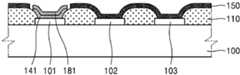
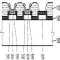
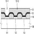
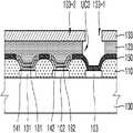
도 1은 본 발명의 제1 실시예에 따른 유기 발광 표시 장치(1)를 개략으로 도시한 단면도이고, 도 2는 본 발명의 제1 실시예에 따른 유기 발광 표시 장치의 일부를 도시한 평면도이다.1 is a schematic cross-sectional view of an organic light emitting
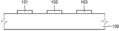
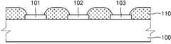
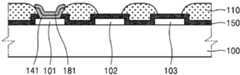
도 1 및 2를 참조하면, 본 실시예에 따른 유기 발광 표시 장치(1)는 기판(100) 상에 제1 애노드(101), 제2 애노드(102), 제3 애노드(103)를 포함하는 복수의 애노드가 서로 이격되어 배치된다.Referring to FIGS. 1 and 2 , an organic light emitting
제1 내지 제3 애노드(101, 102, 103) 상에는 제1 내지 제3 발광층을 포함하는 제1 내지 제3 유기 기능층(141, 142, 143)이 각각 위치하고, 제1 내지 제3 유기 기능층(141, 142, 143) 상에는 도전성 물질을 포함하는 제1 내지 제3 보조 캐소드(181, 182, 183)가 각각 위치한다. 제1 내지 제3 보조 캐소드(181, 182, 183) 상에는 일체로 형성된 공통 전극(180)이 위치한다.On the first to
절연물질로 형성된 화소 정의막(110)은 제1 내지 제3 애노드 (101, 102, 103)의 단부를 커버하여, 각 애노드 단부에서의 전계 집중을 방지한다.The pixel-defining
화소 정의막(110) 상에 자기조립 단분자막(self assembled monolayer)(150)이 제1 내지 제3 유기 기능층(141, 142, 143)의 주위를 둘러싸도록 위치한다. 자기조립 단분자막(150)은 상기 제1 내지 제3 유기 기능층(141,142, 413)의 단부와 소정 간격(D1) 이격되어 위치한다.A self assembled
자기조립 단분자막(150)은 불소를 포함하는 작용기 및 가수분해가 가능한 반응기를 포함할 수 있다.The self-assembled
불소를 포함하는 작용기는 불화카본(-CF3)을 포함할 수 있다. 가수분해가 가능한 반응기는 실리콘 화합물을 포함할 수 있다. 예를 들어, 자기조립 단분자막(150)은 FOTS(1H,1H,2H,2H-perfluorodecyltrichlorosilane-perfluoro), FDTS(heptadecafluoro-1,1,2,2,-tetrahydrodecyl)trichlorosilane), FOMMS(CF3(CF2)5(CH2)2Si(CH3)2Cl), FOMDS(CF3(CF2)5(CH2)2Si(CH3)Cl2), FOTES(CF3(CF2)5(CH2)2Si(OC2H5)3) 등을 포함할 수 있다.The functional group containing fluorine may include fluorocarbon (-CF3). A reactive group capable of hydrolysis may include a silicon compound. For example, the self-assembled
한편, 자기조립 단분자막은 메틸기(-CH)를 포함하는 소수성 작용기를 포함할 수 있다. 예를 들어, 자기조립 단분자막은 OTS(octadecyltrichlorosilane), DDMS(dichlorodimethylsilane) 등을 포함할 수 있다.Meanwhile, the self-assembled monolayer may include a hydrophobic functional group including a methyl group (-CH). For example, the self-assembled monolayer may include octadecyltrichlorosilane (OTS), dichlorodimethylsilane (DDMS), and the like.
불소를 포함하는 작용기는 가수분해가 가능한 반응기보다 제1 내지 제3 애노드(101, 102, 103) 및 화소 정의막(110)의 표면에서 더 먼 거리에 위치할 수 있다. 자기조립 단분자막(150)의 불소를 포함하는 작용기는 후술할, 불소를 포함하는 리프트오프층(121, 도 5a참조)에 대하여 표면 에너지의 차이가 작아, 자기조립 단분자막(150) 위에 리프트오프층(121)을 균일하게 형성함으로써 패터닝 정밀도를 향상시킬 수 있다.Functional groups containing fluorine may be located at a greater distance from the surface of the first to
도 3 내지 도 7f를 참조하여 본 실시예에 따른 유기 발광 표시 장치(1)의 제조 방법 및 상기 제조 방법에 의해 제조된 유기 발광 표시 장치(1)를 보다 상세히 설명한다.A manufacturing method of the organic light emitting
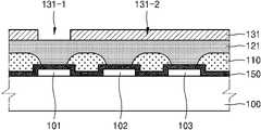
도 3은 본 발명의 제1 실시예에에 따른 유기 발광 표시 장치(1)의 기판 위에 복수의 애노드(101, 102, 103)가 형성된 단계를 개략적으로 도시한 단면도이고, 도 4는 본 발명의 제1 실시예에에 따른 유기 발광 표시 장치(1)에 화소 정의막이 형성된 단계를 개략적으로 도시한 단면도이고, 도 5a 내지 도 5f는 본 발명의 제1 실시예에 따른 유기 발광 표시 장치(1)의 제1 단위 공정을 개략적으로 도시한 단면도들이고, 도 6a 내지 도 6f는 본 발명의 제1 실시예에 따른 유기 발광 표시 장치(1)의 제2 단위 공정을 개략적으로 도시한 단면도들이고, 도 7a 내지 도 7f는 본 발명의 제1 실시예에 따른 유기 발광 표시 장치(1)의 제3 단위 공정을 개략적으로 도시한 단면도들이다.3 is a cross-sectional view schematically illustrating a step of forming a plurality of
도 3을 참조하면, 기판(100) 상에 제1 애노드(101), 제2 애노드(102) 및 제3 애노드(103)을 포함하는 복수의 애노드를 형성한다.Referring to FIG. 3 , a plurality of anodes including a
기판(100)은 다양한 재질을 이용하여 형성할 수 있다. 예를 들면, 기판(100)은 유리 또는 플라스틱을 이용하여 형성할 수 있다. 플라스틱은 폴리이미드 (polyimide), 폴리에틸렌나프탈레이트 (polyethylenenaphthalate), 폴리에틸렌테레프탈레이트 (polyethyleneterephthalate), 폴리아릴레이트 (Polyarylate), 폴리카보네이트 (polycarbonate), 폴리에테르이미드 (Polyetherlmide), 또는 폴리에테르술폰 (Polyethersulfone) 등과 같이 내열성 및 내구성이 우수한 소재로 만들어 질 수 있다.The
도 3에는 도시되어 있지 않으나, 기판(100)의 상부에 평활한 면을 형성하고 불순 원소가 침투하는 것을 차단하기 위한 버퍼층(미도시)을 더 형성할 수 있다. 예들 들어, 버퍼층(미도시)은 실리콘질화물 및/또는 실리콘산화물 등으로 단층 또는 복수층으로 형성할 수 있다.Although not shown in FIG. 3 , a buffer layer (not shown) may be further formed on the
제1 내지 제3 애노드(101, 102, 103)는 정공 주입 전극으로서, 일함수가 큰 재료로 형성될 수 있다. 제1 내지 제3 애노드(101, 102, 103)는 투명도전성산화물 성분을 포함할 수 있다. 예들 들어, 제1 내지 제3 애노드(101, 102, 103)는 인듐틴옥사이드 (indium tin oxide), 인듐징크옥사이드 (indium zinc oxide), 징크옥사이드 (zinc oxide), 인듐옥사이드 (indium oxide), 인듐갈륨옥사이드 (indium gallium oxide), 및 알루미늄징크옥사이드 (aluminum zinc oxide:)을 포함하는 부화소에서 선택된 적어도 하나 이상을 포함할 수 있다. 또한, 제1 내지 제3 애노드(101, 102, 103)은 은(Ag), 알루미늄, 마그네슘, 리튬, 칼슘 등의 금속 및/또는 합금으로 단층 또는 복수층으로 형성할 수 있다.The first to
도 3에는 도시되어 있지 않으나 제1 내지 제3 애노드(101, 102, 103)는 기판(100)과 제1 내지 제3 애노드(101, 102, 103) 사이에 위치하는 제1 내지 제3 박막트랜지스터(미도시)에 각각 전기적으로 접속되도록 형성될 수 있다.Although not shown in FIG. 3 , the first to
도 4를 참조하면, 기판(100) 상에 제1 애노드(101), 제2 애노드(102) 및 제3 애노드(103)의 가장자리를 둘러싸는 화소 정의막(110)을 형성한다.Referring to FIG. 4 , a
제1 내지 제3 애노드(101, 102, 103)는 단부가 뽀죡한 형태이기 때문에 제1 내지 제3 보조 캐소드(181, 182, 183) 형성 후 전류를 인가할 시, 제1 내지 제3 애노드(101, 102, 103)의 단부에 전계가 집중되어 구동 중 전기적 단락이 발생할 수 있다. 그러나 본 실시예에서는 제1 내지 제3 애노드(101, 102, 103)의 단부를 화소 정의막(110)이 덮어 단부에 전계가 집중되는 현상을 완화한다.Since the first to
화소 정의막(110)은 예를 들어, 일반 범용고분자(PMMA, PS), phenol부화소를 갖는 고분자 유도체, 아크릴계 고분자, 이미드계 고분자, 아릴에테르계 고분자, 아마이드계 고분자, 불소계고분자, p-자일렌계 고분자, 비닐알콜계 고분자 및 이들의 블렌드 등을 포함하는 유기 절연막으로 형성될 수 있다.The pixel-defining
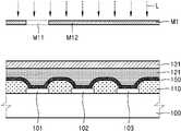
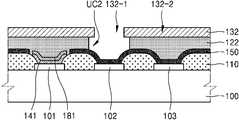
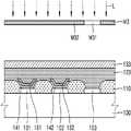
도 5a를 참조하면, 제1 내지 제3 애노드(101, 102, 103)가 형성된 기판(100) 상에 자기조립 단분자막(150), 제1 리프트오프층(121), 및 제1 포토레지스트(131)가 순차로 형성된다.Referring to FIG. 5A , a self-assembled
자기조립 단분자막(150)은 도포법, 인쇄법, 증착법 등의 방법으로 형성할 수 있다. 자기조립 단분자막(150)은 전술한 바와 같이, 불소를 포함하는 작용기 및 가수분해가 가능한 반응기를 포함할 수 있다. 예를 들어, 자기조립 단분자막(150)은 FOTS(1H,1H,2H,2H-perfluorodecyltrichlorosilane-perfluoro), FDTS(heptadecafluoro-1,1,2,2,-tetrahydrodecyl)trichlorosilane), FOMMS(CF3(CF2)5(CH2)2Si(CH3)2Cl), FOMDS(CF3(CF2)5(CH2)2Si(CH3)Cl2), FOTES(CF3(CF2)5(CH2)2Si(OC2H5)3) 등을 포함할 수 있다.The self-assembled
제1 리프트오프층(121)은 불소 중합체를 포함한다. 제1 리프트오프층(121)에 포함되는 불소중합체(fluoroplymer)는 20~60 wt%의 불소 함량을 포함하는 고분자(polymer)로 형성할 수 있다. 예를 들어, 제1 리프트오프층(121)에 포함되는 불소중합체는 폴리테트라플루오로에틸렌 (polytetrafluoroethylene,), 폴리클로로트리플루오로에틸렌 (polychlorotrifluoroethylene,), 폴리디클로로디플루오로에틸렌 (polydichlorodifluoroethylene), 클로로트리플루오로에틸렌 (chlorotrifluoroethylene)과 디클로로디플루오로에틸렌과의 공중합체, 테트라플루오로에틸렌 (tetrafluoroethylene)과 퍼플루오로알킬비닐에테르 (perfluoroalkylvinylether)와의 공중합체, 클로로트리플루오로에틸렌 (chlorotrifluoroethylene)과 퍼플루오로알킬비닐에테르 (perfluoroalkylvinylether)와의 공중합체, 테트라플루오로에틸렌 (tetrafluoroethylene)과 퍼플루오로알킬비닐에테르(perfluoroalkylvinylether)와의 공중합체, 또는 클로로트리플루오로에틸렌 (chlorotrifluoroethylene)과 퍼플루오로알킬비닐에테르 (perfluoroalkylvinylether)와의 공중합체 중 적어도 하나를 포함할 수 있다.The first lift-
제1 리프트오프층(121)은 도포법, 인쇄법, 증착법 등의 방법으로 형성할 수 있다. 도포법과 인쇄법으로 제1 리프트오프층(121)을 형성할 경우, 필요에 따라 경화, 중합 처리를 한 후 제1 포토레지스트(131)를 형성하는 공정을 진행할 수 있다.The first lift-
도 21은 제1 애노드 위에 자기조립 단분자막(150)을 형성할 경우, 자기조립 단분자막(150)이 작동하는 메커니즘을 간략하게 도시한 것이다.21 schematically illustrates a mechanism in which the self-assembled
예를 들어, 인듐틴옥사이드로 형성된 제1 애노드(101) 위에, FOTS를 포함하는 자기조립 단분자막(150)을 증착할 경우, 자기조립 단분자막(150)의 실리콘을 포함하는 가수분해 반응기는 제1 애노드(101) 표면의 수산화기(-OH)와 가수 분해 및 축합 반응이 일어나고, 자기조립 단분자막(150)은 제1 애노드(101)의 표면과 공유결합하게 된다. 이러한 공유결합은 자기조립 단분자막(150)과 제1 애노드(101)의 표면간 접착력을 증가시킨다.For example, when the self-assembled
자기조립 단분자막(150) 위에 불소중합체를 포함하는 제1 리프트오프층(121)이 형성될 경우, 제1 리프트오프층(121)과 가까이 접하는 자기조립 단분자막(150)의 불소를 포함하는 작용기는, 제1 리프트오프층(121)에 대하여 표면 에너지의 차이가 작아, 자기조립 단분자막(150) 위에 리프트오프층(121)을 균일하게 형성할 수 있다.When the first lift-
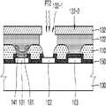
제1 리프트오프층(121) 상에 제1 포토레지스트(131)를 형성한다. 광(L)을 투과시키는 영역(M11)을 포함하는 제1 포토마스크(M1)를 통하여 제1 애노드(101)에 대응되는 위치의 제1 포토레지스트(131)를 노광 시킨다.A
도 5b를 참조하면, 제1 포토레지스트(131)를 현상(develop)한다. 제1 포토레지스트(131)는 포지티브 형 또는 네가티브 형 어느 것도 가능하다. 본 실시예에서는 포지티브 형을 예로 설명한다. 현상된 제1 포토레지스트(131)는 제1 애노드(101)에 대응하는 위치인 제1 부분 (131-1)이 제거되고, 나머지 제2 부분(131-2)은 잔존한다.Referring to FIG. 5B , the
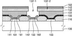
도 5c를 참조하면, 도 5b의 제1 포토레지스트(131)의 제1 영역(131-1) 패턴을 식각 마스크로 하여 제1 리프트오프층(121)을 에칭한다.Referring to FIG. 5C , the first lift-
제1 리프트오프층(121)이 불소중합체를 포함하고 있기 때문에 식각액은 불소중합체를 식각 할 수 있는 용매를 사용한다.Since the first lift-
식각액은 불소를 포함하는 제1 용매(미도시)를 사용할 수 있다. 제1 용매는 히드로플루오로에테르(hydrofluoroether)를 포함할 수 있다. 히드로플루오로에테르는 다른 소재와의 상호작용이 낮아 전자화학적으로 안정적인 재료이고, 지구 온난화 계수와 독성이 낮아서 환경적으로 안정적인 재료이다.The etchant may use a first solvent (not shown) containing fluorine. The first solvent may include hydrofluoroether. Hydrofluoroether is an electrochemically stable material due to its low interaction with other materials, and an environmentally stable material due to its low global warming coefficient and low toxicity.
식각 공정에 의해, 제1 부분(131-1)에 대응하는 위치, 즉 제1 애노드(101) 상부에 형성된 제1 리프트오프층(121)이 식각된다. 제1 리프트오프층(121) 에칭 시, 불소를 포함하는 제1 용매는 제1 포토레지스트(131)의 제1 부분(131-1)의 경계면 아래에서 제1 언더컷 프로파일(UC1-1)을 형성한다.Through the etching process, the first lift-
제1 리프트오프층(121)이 식각되는 동안 자기조립 단분자막(150)은 제1 애노드(101)의 상면에 잘 결합되어 있다. 전술한 바와 같이, 자기조립 단분자막(150)에 포함된 실리콘을 포함하는 반응기와 제1 애노드(101) 표면 사이에서 가수 분해 및 축합 반응이 일어나, 자기조립 단분자막(150)과 제1 애도드(101) 표면과의 사이에 공유결합에 의한 접착력이 증가하기 때문이다.While the first lift-
한편, 자기조립 단분자막(150)에 포함된 실리콘을 포함하는 반응기는 화소 정의막(110)의 표면물질과 가수부해 및 축합 반응으로 양 구성요소의 표면간 접착력이 증가하기 때문에, 제1 리프트오프층(121)이 식각되는 동안 자기조립 단분자막(150)은 화소 정의막(110)의 상면에 잘 결합되어 있다.On the other hand, since the silicon-containing reactor included in the self-assembled
도 5d를 참조하면, 도 5c의 구조물에 제1 플라즈마 열처리로 제1 애도느 상의 자기조립 단분자막(150)을 제거한다.Referring to FIG. 5D , the self-assembled
도 21에 도시된 바와 같이, 플라즈마 열처리에 의해 제1 애노드(101)와 자기조립 단분자막(150) 사이의 Si-O 결합이 깔끔하게 끊어진다. 만약, 자기조립 단분자막(150)을 형성하지 않고, 제1 애노드(101) 형성 후, 제1 애노드(101) 위에 제1 리프트오프층(121)을 직접 형성하고 후 공정에서 제거할 경우, 제1 애노드(101) 위에 제1 리프트오프층(121)의 잔사가 남아 오염을 일으킨다. 그러나, 본 실시예에서는 제1 애노드(101)와 제1 리프트오프층(121) 사이에 자기조립 단분자막(150)을 형성함으로써, 제1 애노드(101) 상에 제1 리프트오프층(121)을 잔사를 방지함으로써 유기 발광 표시 장치의 열화를 방지할 수 있다.As shown in FIG. 21 , the Si—O bond between the
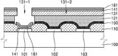
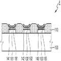
도 5e를 참조하면, 도 5d의 구조물 상에 제1 발광층(미도시)을 포함하는 제1 유기 기능층(141) 및 제1 보조 캐소드(181)를 순차로 형성한다.Referring to FIG. 5E , a first organic
제1 유기 기능층(141)은 정공 주입층(hole injection layer), 정공 수송층(hole transport layer), 전자 수송층(electron transport layer), 및 전자 주입층(electron injection layer) 중 적어도 하나의 기능층을 더 포함할 수 있다.The first organic
제1 유기 기능층(141)은 진공 증착 방법으로 형성될 수 있다. 증착 공정에서, 제1 리프트오프층(121) 및 제1 포토레지스트(131)가 마스크 기능을 한다. 제1 유기 기능층(141)의 일부는 제1 부분(131-1)에 대응하는 위치 즉 제1 애노드(101) 상부에 형성되고, 제1 유기 기능층(141)의 다른 부분은 제1 포토레지스트(131)의 제2 부분(131-2) 상에 형성된다.The first organic
제1 보조 캐소드(181)는 제1 유기 기능층(141)과 마찬가지로 진공 증착 방법으로 형성될 수 있다. 증착 공정에서, 제1 리프트오프층(121)과 제1 포토레지스트(131)가 마스크 기능을 한다. 제1 보조 캐소드(181)의 일부는 제1 유기 기능층(141)의 상면을 덮도록 형성된다. 그리고, 제1 보조 캐소드(181)의 다른 일부는 제1 부분(131-1)을 제외한 제1 포토레지스트(131)의 나머지 영역인 제2 부분(131-2)에서 제1 유기 기능층(141) 위에 형성된다.Like the first organic
제1 보조 캐소드(181)는 후술할 공통전극으로서의 캐소드(180)와 동일한 재료를 포함할 수 있다. 또한, 제1 보조 캐소드(181)는 캐소드(180)와 다른 재료로 형성될 수 있다. 제1 보조 캐소드(181)는 후술할 리프트오프 공정에서 사용되는 용매로부터 제1 유기 기능층(141)을 보호하는 배리어 역할을 할 수 있다.The first
도 5f를 참조하면, 도 5e의 구조물에 대하여 리프트 오프 공정을 수행한다.Referring to FIG. 5F, a lift-off process is performed on the structure of FIG. 5E.
제1 리프트오프층(121)은 불소중합체를 포함하고 있기 때문에, 리프트 오프 공정에 불소를 포함하는 제2 용매를 사용한다. 한편, 제1 유기 기능층(141)을 형성한 다음에 리프트 오프 공정을 실시하기 때문에, 제2 용매는 제1 유기 기능층(141)과의 반응성이 낮은 재료를 사용하는 것이 바람직하다. 제2 용매는 제1 용매와 같이 히드로플루오로에테르(hydrofluoroether)를 포함할 수 있다.Since the first lift-
제1 포토레지스트(131)의 제2 부분(131-2, 도 5e) 하부에 형성된 제1 리프트오프층(121)을 리프트 오프 시킴으로써, 제1 포토레지스트(131)의 제2 부분(131-2, 도 5e) 위에 형성된 제1 유기 기능층(141) 및 제1 보조 캐소드(181)는 제거되고, 제1 애노드(101) 위에 형성된 제1 유기 기능층(141)과 제1 보조 캐소드(181)가 패턴으로 남는다.The second portion 131-2 of the
한편, 화소 정의막(110) 위에 형성된 자기조립 단분자막(150)은 제거되지 않는다. 전술한 대로, 자기조립 단분자막(150)에 포함된 실리콘을 포함하는 반응기는 화소 정의막(110)의 표면물질과 가수부해 및 축합 반응으로 양 구성요소의 표면간 접착력이 증가하기 때문에, 제1 리프트오프층(121)이 리프트 오프 되는 동안 자기조립 단분자막(150)은 화소 정의막(110)의 상면에 잘 결합되어 있다Meanwhile, the self-assembled
상술한 제1 단위 공정을 실시한 후, 제2 애노드(102)가 위치하는 영역에, 제1 유기 기능층(141)과 다른 색의 광을 방출하는 제2 유기 기능층(142)을 형성하는 제2 단위 공정을 실시한다. 이하, 도 6a 내지 도 6f를 참조하여 제2 단위 공정을 설명한다.After performing the above-described first unit process, the second organic
도 6a를 참조하면, 도 5f의 구조물 상에 제2 리프트오프층(122), 및 제2 포토레지스트(132)를 순차로 형성된다.Referring to FIG. 6A , a second lift-
제2 리프트오프층(122)은 불소 중합체를 포함한다. 제2 리프트오프층(122)은 전술한 제1 리프트오프층(121)과 동일한 물질을 포함할 수 있으며, 도포법, 인쇄법, 증착법 등의 방법으로 형성할 수 있다.The second lift-
제2 리프트오프층(122) 상에 제2 포토레지스트(132)를 형성한다. 광(L)을 투과시키는 영역(M21)을 포함하는 제2 포토마스크(M2)를 통하여 제2 애노드(102)에 대응되는 위치의 제2 포토레지스트(132)를 노광 시킨다.A
도 6b를 참조하면, 제2 포토레지스트(132)를 현상하여 제2 포토레지스트(132)는 제2 애노드(102)에 대응하는 위치인 제1 부분 (132-1)이 제거되고, 나머지 제2 부분(132-2)은 잔존한다.Referring to FIG. 6B, by developing the
도 6c를 참조하면, 도 6b의 제2 포토레지스트(132)의 제1 영역(132-1) 패턴을 식각 마스크로 하여 제2 리프트오프층(122)을 에칭한다.Referring to FIG. 6C , the second lift-
제2 리프트오프층(122)이 불소중합체를 포함하고 있기 때문에 식각액은 불소중합체를 식각 할 수 있는 용매를 사용한다. 식각액은 불소를 포함하는 제1 용매(미도시)를 사용할 수 있다. 제1 용매는 히드로플루오로에테르(hydrofluoroether)를 포함할 수 있다.Since the second lift-
식각 공정에 의해, 제1 부분(132-1)에 대응하는 위치, 즉 제2 애노드(102) 상부에 형성된 제2 리프트오프층(122)이 식각된다. 제2 리프트오프층(122) 에칭 시, 불소를 포함하는 제1 용매는 제2 포토레지스트(132)의 제1 부분(132-1)의 경계면 아래에서 제1 언더컷 프로파일(UC2-1)을 형성한다.Through the etching process, the second lift-
제2 리프트오프층(122)이 식각되는 동안 자기조립 단분자막(150)은 제2 애노드(102)의 상면에 잘 결합되어 있다. 또한 제2 리프트오프층(122)이 식각되는 동안 자기조립 단분자막(150)은 화소 정의막(110)의 상면에 잘 결합되어 있다While the second lift-
도 6d를 참조하면, 도 6c의 구조물에 제2 플라즈마 열처리로 제2 애도느 상의 자기조립 단분자막(150)을 제거한다.Referring to FIG. 6D , the self-assembled
제2 플라즈마 열처리(PT2)에 의해 제2 애노드(102)와 자기조립 단분자막(150) 사이의 Si-O 결합이 깔끔하게 끊어진다. 따라서, 제2 애노드(102) 상에 제2 리프트오프층(122)의 잔사가 남지 않는다.The Si—O bond between the
도 6e를 참조하면, 도 6d의 구조물 상에 제2 발광층(미도시)을 포함하는 제2 유기 기능층(142) 및 제2 보조 캐소드(182)를 순차로 형성한다.Referring to FIG. 6E , a second organic
제2 유기 기능층(142)은 정공 주입층(hole injection layer), 정공 수송층(hole transport layer), 전자 수송층(electron transport layer), 및 전자 주입층(electron injection layer) 중 적어도 하나의 기능층을 더 포함할 수 있다.The second organic
제2 유기 기능층(142)은 진공 증착 방법으로 형성될 수 있다. 증착 공정에서, 제2 리프트오프층(122) 및 제2 포토레지스트(132)가 마스크 기능을 한다. 제2 유기 기능층(142)의 일부는 제1 부분(132-1)에 대응하는 위치 즉 제2 애노드(102) 상부에 형성되고, 제2 유기 기능층(142)의 다른 부분은 제2 포토레지스트(132)의 제2 부분(132-2) 상에 형성된다.The second organic
제2 보조 캐소드(182)는 제2 유기 기능층(142)과 마찬가지로 진공 증착 방법으로 형성될 수 있다. 증착 공정에서, 제2 리프트오프층(122)과 제2 포토레지스트(132)가 마스크 기능을 한다. 제2 보조 캐소드(182)의 일부는 제2 유기 기능층(142)의 상면을 덮도록 형성된다. 그리고, 제2 보조 캐소드(182)의 다른 일부는 제1 부분(132-1)을 제외한 제2 포토레지스트(132)의 나머지 영역인 제2 부분(132-2)에서 제2 유기 기능층(142) 위에 형성된다.Like the second organic
제2 보조 캐소드(182)는 후술할 공통전극으로서의 캐소드(180)와 동일한 재료를 포함할 수 있다. 또한, 제2 보조 캐소드(182)는 캐소드(180)와 다른 재료로 형성될 수 있다. 제2 보조 캐소드(182)는 후술할 리프트오프 공정에서 사용되는 용매로부터 제2 유기 기능층(142)을 보호하는 배리어 역할을 할 수 있다.The second
도 6f를 참조하면, 도 6e의 구조물에 대하여 리프트 오프 공정을 수행한다.Referring to FIG. 6F, a lift-off process is performed on the structure of FIG. 6E.
제2 리프트오프층(122)은 불소중합체를 포함하고 있기 때문에, 리프트 오프 공정에 불소를 포함하는 제2 용매를 사용한다. 한편, 제2 유기 기능층(142)을 형성한 다음에 리프트 오프 공정을 실시하기 때문에, 제2 용매는 제2 유기 기능층(142)과의 반응성이 낮은 재료를 사용하는 것이 바람직하다. 제2 용매는 제1 용매와 같이 히드로플루오로에테르(hydrofluoroether)를 포함할 수 있다.Since the second lift-
제2 포토레지스트(132)의 제2 부분(132-2, 도 6e) 하부에 형성된 제2 리프트오프층(122)을 리프트 오프 시킴으로써, 제2 포토레지스트(132)의 제2 부분(132-2, 도 6e) 위에 형성된 제2 유기 기능층(142) 및 제2 보조 캐소드(182)는 제거되고, 제2 애노드(102) 위에 형성된 제2 유기 기능층(142)과 제2 보조 캐소드(182)가 패턴으로 남는다.The second portion 132-2 of the
한편, 전술한 바와 마찬가지로 자기조립 단분자막(150)과 화소 정의막(150) 사이의 결"W력이 좋기 때문에, 제2 리프트오프층(121)이 리프트오프 되는 동안, 화소 정의막(110) 위에 형성된 자기조립 단분자막(150)은 제거되지 않는다.Meanwhile, as described above, since the bonding force between the self-assembled
상술한 제2 단위 공정을 실시한 후, 제3 애노드(103)가 위치하는 영역에, 제1 유기 기능층(141) 및 제2 유기 기능층(142)과 다른 색의 광을 방출하는 제3 유기 기능층(143)을 형성하는 제3 단위 공정을 실시한다. 이하, 도 7a 내지 도 7f를 참조하여 제3 단위 공정을 설명한다.After performing the above-described second unit process, the third organic
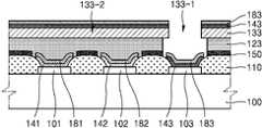
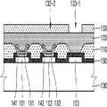
도 7a를 참조하면, 도 6f의 구조물 상에 제3 리프트오프층(123), 및 제3 포토레지스트(133)를 순차로 형성된다.Referring to FIG. 7A, a third lift-
제3 리프트오프층(123)은 불소 중합체를 포함한다. 제3 리프트오프층(123)은 전술한 제1 및 제2 리프트오프층(121, 122)과 동일한 물질을 포함할 수 있으며, 도포법, 인쇄법, 증착법 등의 방법으로 형성할 수 있다.The third lift-
제3 리프트오프층(123) 상에 제3 포토레지스트(133)를 형성한다. 광(L)을 투과시키는 영역(M31)을 포함하는 제3 포토마스크(M3)를 통하여 제3 애노드(103)에 대응되는 위치의 제3 포토레지스트(133)를 노광 시킨다.A
도 7b를 참조하면, 제3 포토레지스트(133)를 현상한다. 제3 포토레지스트(133)는 제3 애노드(103)에 대응하는 위치인 제1 부분 (133-1)이 제거되고, 나머지 제2 부분(133-2)은 잔존한다.Referring to FIG. 7B , the
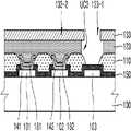
도 7c를 참조하면, 도 7b의 제3 포토레지스트(133)의 제1 영역(133-1) 패턴을 식각 마스크로 하여 제3 리프트오프층(123)을 에칭한다.Referring to FIG. 7C , the third lift-
제3 리프트오프층(123)이 불소중합체를 포함하고 있기 때문에 식각액은 불소중합체를 식각 할 수 있는 용매를 사용한다. 식각액은 불소를 포함하는 제1 용매(미도시)를 사용할 수 있다. 제1 용매는 히드로플루오로에테르(hydrofluoroether)를 포함할 수 있다.Since the third lift-
식각 공정에 의해, 제1 부분(133-1)에 대응하는 위치, 즉 제3 애노드(103) 상부에 형성된 제3 리프트오프층(123)이 식각된다. 제3 리프트오프층(123) 에칭 시, 불소를 포함하는 제1 용매는 제3 포토레지스트(133)의 제1 부분(133-1)의 경계면 아래에서 제1 언더컷 프로파일(UC3-1)을 형성한다.Through the etching process, the third lift-
제3 리프트오프층(123)이 식각되는 동안 자기조립 단분자막(150)은 제3 애노드(103)의 상면에 잘 결합되어 있다. 또한 제3 리프트오프층(123)이 식각되는 동안 자기조립 단분자막(150)은 화소 정의막(110)의 상면에 잘 결합되어 있다While the third lift-
도 7d를 참조하면, 도 7c의 구조물에 제3 플라즈마 열처리로 제3 애도느 상의 자기조립 단분자막(150)을 제거한다.Referring to FIG. 7D , the self-assembled
제3 플라즈마 열처리(PT3)에 의해 제3 애노드(103)와 자기조립 단분자막(150) 사이의 Si-O 결합이 깔끔하게 끊어진다. 따라서, 제3 애노드(103) 상에 제3 리프트오프층(123)의 잔사가 남지 않는다.The Si—O bond between the
도 7e를 참조하면, 도 7d의 구조물 상에 제3 발광층(미도시)을 포함하는 제3 유기 기능층(143) 및 제3 보조 캐소드(183)를 순차로 형성한다.Referring to FIG. 7E , a third organic
제3 유기 기능층(143)은 정공 주입층(hole injection layer), 정공 수송층(hole transport layer), 전자 수송층(electron transport layer), 및 전자 주입층(electron injection layer) 중 적어도 하나의 기능층을 더 포함할 수 있다.The third organic
제3 유기 기능층(143)은 진공 증착 방법으로 형성될 수 있다. 증착 공정에서, 제3 리프트오프층(123) 및 제3 포토레지스트(133)가 마스크 기능을 한다. 제3 유기 기능층(143)의 일부는 제1 부분(133-1)에 대응하는 위치 즉 제3 애노드(103) 상부에 형성되고, 제3 유기 기능층(143)의 다른 부분은 제3 포토레지스트(133)의 제2 부분(133-2) 상에 형성된다.The third organic
제3 보조 캐소드(183)는 제3 유기 기능층(143)과 마찬가지로 진공 증착 방법으로 형성될 수 있다. 증착 공정에서, 제3 리프트오프층(123)과 제3 포토레지스트(133)가 마스크 기능을 한다. 제3 보조 캐소드(183)의 일부는 제3 유기 기능층(143)의 상면을 덮도록 형성된다. 그리고, 제3 보조 캐소드(183)의 다른 일부는 제1 부분(133-1)을 제외한 제3 포토레지스트(133)의 나머지 영역인 제2 부분(133-2)에서 제3 유기 기능층(143) 위에 형성된다.Like the third organic
제3 보조 캐소드(183)는 후술할 공통전극으로서의 캐소드(180)와 동일한 재료를 포함할 수 있다. 또한, 제3 보조 캐소드(182)는 캐소드(180)와 다른 재료로 형성될 수 있다. 제3 보조 캐소드(183)는 후술할 리프트오프 공정에서 사용되는 용매로부터 제3 유기 기능층(143)을 보호하는 배리어 역할을 할 수 있다.The third
도 7f를 참조하면, 도 6e의 구조물에 대하여 리프트 오프 공정을 수행한다.Referring to FIG. 7F, a lift-off process is performed on the structure of FIG. 6E.
제3 리프트오프층(123)은 불소중합체를 포함하고 있기 때문에, 리프트 오프 공정에 불소를 포함하는 제2 용매를 사용한다. 한편, 제3 유기 기능층(143)을 형성한 다음에 리프트 오프 공정을 실시하기 때문에, 제2 용매는 제3 유기 기능층(143)과의 반응성이 낮은 재료를 사용하는 것이 바람직하다. 제2 용매는 제1 용매와 같이 히드로플루오로에테르(hydrofluoroether)를 포함할 수 있다.Since the third lift-
제3 포토레지스트(133)의 제2 부분(133-2, 도 7e) 하부에 형성된 제3 리프트오프층(123)을 리프트 오프 시킴으로써, 제3 포토레지스트(133)의 제2 부분(133-2, 도 7e) 위에 형성된 제3 유기 기능층(143) 및 제3 보조 캐소드(183)는 제거되고, 제3 애노드(103) 위에 형성된 제3 유기 기능층(143)과 제3 보조 캐소드(183)가 패턴으로 남는다.The second portion 133-2 of the
한편, 전술한 바와 마찬가지로 자기조립 단분자막(150)과 화소 정의막(150) 사이의 결합력이 좋기 때문에, 제3 리프트오프층(131)이 리프트오프 되는 동안, 화소 정의막(110) 위에 형성된 자기조립 단분자막(150)은 제거되지 않는다.Meanwhile, as described above, since the bonding force between the self-assembled
상기 제1 내지 제3 유기 기능층(141, 142, 143)은 서로 다른 색의 빛을 방출할 수 있다. 제1 내지 제3 유기 기능층(141, 142, 143)에서 방출되는 빛은 혼합하면 백색광을 형성할 수 있다. 예를 들어, 제1 내지 제3 유기 기능층(141, 142, 143)은 적색, 녹색 및 청색의 빛을 방출할 수 있다. 예를 들어, 제1 내지 제3 유기 기능층(141, 142, 143)은 유기 발광 표시 장치(1)의 단위 화소를 구성하는 부화소의 구성일 수 있다.The first to third organic
또한 도 1에 도시된 유기 발광 표시 장치(1)는 하나의 단위 화소를 나타내는 것일 수 있다. 또한, 본 실시예는 도 1에 도시된 단위 화소를 복수개 구비하는 유기 발광 표시 장치에도 적용될 수 있다. 즉, 제1 단위 공정으로 제1 색을 방출하는 제1 유기 기능층(141)은 제1 부화소로서 복수개가 동시에 형성될 수 있다. 제2 단위 공정으로 제2 색을 방출하는 제2 유기 기능층(142)은 제2 부화소로서 복수개가 동시에 형성될 수 있다. 제3 단위 공정으로 제3 색을 방출하는 제3 유기 기능층(143)은 제3 부화소로서 복수개가 동시에 형성될 수 있다. 제1 내지 제3 단위 공정을 통하여, 풀 컬러를 구현할 수 있다.Also, the organic light emitting
본 실시예에서, 리프트오프층을 애노드 위에 직접 형성하지 않고, 애노드와 리프트오프층 사이에 자기조립 단분자막을 형성함으로써, 리프트오프층이 애노드 위에 잔막을 형성하는 것을 원천적으로 방지하여 유기 발광 표시 장치의 열화를 방지할 수 있다.In this embodiment, the lift-off layer is not directly formed on the anode, but a self-assembled monolayer is formed between the anode and the lift-off layer to fundamentally prevent the lift-off layer from forming a residual film on the anode, thereby improving the quality of the organic light emitting display device. Deterioration can be prevented.
이하 도 18a 내지 20e의 비교예에 따른 유기 발광 표시 장치(4)의 제조 방법과 비교하여 설명한다.Hereinafter, a method of manufacturing the organic light emitting
도 18a 내지 도 18e는 비교예에 따른 유기 발광 표시 장치(4)의 제1 단위 공정을 개략적으로 도시한 단면도들이고, 도 19a 내지 도 19e는 비교예에 따른 유기 발광 표시 장치의 제2 단위 공정을 개략적으로 도시한 단면도들이고, 도 20a 내지 도 20e는 비교예에 따른 유기 발광 표시 장치의 제3 단위 공정을 개략적으로 도시한 단면도들이다.18A to 18E are cross-sectional views schematically illustrating a first unit process of an organic light emitting
도 18a를 참조하면, 제1 내지 제3 애노드(101, 102, 103)와 제1 내지 제3 애노드 (101, 102, 103)의 단부를 커버하는 화소 정의막(110)이 형성된 기판(100) 상에 불소중합체(fluoropolymer)를 포함하는 제1 리프트오프층(121)을 형성하고, 제1 리프트오프층(121) 상에 제1 포토레지스트(131)를 형성한다. 광(L)을 투과시키는 영역(M11)을 포함하는 제1 포토마스크(M1)를 통하여 제1 애노드(101)에 대응되는 위치의 제1 포토레지스트(131)를 노광 시킨다.Referring to FIG. 18A, a
도 18b를 참조하면, 제1 포토레지스트(131)가 패터닝된 형상을 도시하고 있다. 노광 및 현상된 제1 포토레지스트(131)는 제1 애노드(101)에 대응하는 위치인 제1 부분 (131-1)에서 제거되고, 제1 부분(131-1)의 나머지 영역인 제2 부분(131-2)에서 잔존한다.Referring to FIG. 18B , a patterned shape of the
도 18c를 참조하면, 도 18b의 제1 포토레지스트(131) 패턴을 식각 마스크로 하여 제1 리프트오프층(121)을 불소를 포함하는 제1 용매(미도시)를 사용하여 식각한다. 식각 공정에 의해, 제1 부분(131-1)에 대응하는 위치, 즉 제1 애노드(101) 상부에 형성된 제1 리프트오프층(121)이 식각된다. 제1 리프트오프층(121)은 제1 포토레지스트(131)의 제1 부분(131-1)의 경계면 아래에서 제1 언더컷 프로파일(UC1)을 형성한다. 식각 공정 후 제1 리프트오프층(121)의 스트립 시, 제1 애노드(101) 위에 리프트오프층의 잔사가 남는다.Referring to FIG. 18C , the first lift-
도 18d를 참조하면, 도 18c의 구조물 상에 제1 유기 기능층(141) 및 제1 보조 캐소드(181)를 순차로 형성한다.Referring to FIG. 18D, a first organic
도 18e를 참조하면, 제1 리프트오프 공정을 진행하여 잔존하는 제1 리프트오프층(121)을 모두 제거하고, 그 결과 제1 애노드(101) 위의 제1 유기 기능층(141) 및 제1 보조 캐소드(181)가 패턴으로 남는다.Referring to FIG. 18E, a first lift-off process is performed to remove all of the remaining first lift-
제1 단위공정 완료 후, 제2 애노드(102)가 위치하는 영역에 제2 단위 공정을 실시한다.After the first unit process is completed, a second unit process is performed in the region where the
도 19a를 참조하면, 도 18e의 구조물에 제2 리프트오프층(122) 및 제2 포토레지스트(132)를 차례로 형성한다.Referring to FIG. 19A, a second lift-
도 19b를 참조하면, 제2 포토레지스트(132)가 패터닝된 형상을 도시하고 있다. 노광 및 현상된 제2 포토레지스트(132)는 제2 애노드(102)에 대응하는 위치인 제1 부분 (132-1)에서 제거되고, 제1 부분(132-1)의 나머지 영역인 제2 부분(132-2)에서 잔존한다.Referring to FIG. 19B , a patterned shape of the
도 19c를 참조하면, 도 19b의 제2 포토레지스트(132) 패턴을 식각 마스크로 하여 제2 리프트오프층(122)을 불소를 포함하는 제1 용매(미도시)를 사용하여 식각한다. 식각 공정에 의해, 제1 부분(132-1)에 대응하는 위치, 즉 제2 애노드(102) 상부에 형성된 제2 리프트오프층(122)이 식각된다. 제2 리프트오프층(122)은 제2 포토레지스트(132)의 제1 부분(132-1)의 경계면 아래에서 제2 언더컷 프로파일(UC2)을 형성한다. 식각 공정 후 제2 리프트오프층(122)의 스트립 시, 제2 애노드(102) 위에 리프트오프층의 잔사가 남는다.Referring to FIG. 19C , the second lift-
도 19d를 참조하면, 도 19c의 구조물 상에 제2 유기 기능층(142) 및 제2 보조 캐소드(182)를 순차로 형성한다.Referring to FIG. 19D, a second organic
도 19e를 참조하면, 제2 리프트오프 공정을 진행하여 잔존하는 제2 리프트오프층(122)을 모두 제거하고, 그 결과 제2 애노드(102) 위의 제2 유기 기능층(142) 및 제2 보조 캐소드(182)가 패턴으로 남는다.Referring to FIG. 19E, a second lift-off process is performed to remove all of the remaining second lift-
제2 단위공정 완료 후, 제3 애노드(103)가 위치하는 영역에 제3 단위 공정을 실시한다.After the second unit process is completed, the third unit process is performed in the region where the
도 20a를 참조하면, 도 19e의 구조물에 제3 리프트오프층(123) 및 제3 포토레지스트(133)를 차례로 형성한다.Referring to FIG. 20A, a third lift-
도 20b를 참조하면, 제3 포토레지스트(133)가 패터닝된 형상을 도시하고 있다. 노광 및 현상된 제3 포토레지스트(133)는 제3 애노드(103)에 대응하는 위치인 제1 부분 (133-1)에서 제거되고, 제1 부분(133-1)의 나머지 영역인 제2 부분(133-2)에서 잔존한다.Referring to FIG. 20B , a patterned shape of the
도 20c를 참조하면, 도 20b의 제3 포토레지스트(133) 패턴을 식각 마스크로 하여 제3 리프트오프층(123)을 불소를 포함하는 제1 용매(미도시)를 사용하여 식각한다. 식각 공정에 의해, 제1 부분(133-1)에 대응하는 위치, 즉 제3 애노드(103) 상부에 형성된 제3 리프트오프층(123)이 식각된다. 제3 리프트오프층(123)은 제3 포토레지스트(133)의 제1 부분(133-1)의 경계면 아래에서 제3 언더컷 프로파일(UC3)을 형성한다. 식각 공정 후 제3 리프트오프층(123)의 스트립 시, 제3 애노드(103) 위에 리프트오프층의 잔사가 남는다.Referring to FIG. 20C , the third lift-
도 20d를 참조하면, 도 20c의 구조물 상에 제3 유기 기능층(143) 및 제3 보조 캐소드(183)를 순차로 형성한다.Referring to FIG. 20D, a third organic
도 20e를 참조하면, 제3 리프트오프 공정을 진행하여 잔존하는 제3 리프트오프층(123)을 모두 제거하고, 그 결과 제3 애노드(103) 위의 제3 유기 기능층(143) 및 제3 보조 캐소드(183)가 패턴으로 남는다.Referring to FIG. 20E, a third lift-off process is performed to remove all of the remaining third lift-
즉 비교예에 따르면, 애노드 위에 직접 리프트오프층을 형성하여 패터닝함으로써, 리프트오프층이 애노드 위에 잔막을 형성하는 것을 원천적으로 방지할 수 없다.That is, according to the comparative example, by forming and patterning the lift-off layer directly on the anode, it is impossible to fundamentally prevent the lift-off layer from forming a residual film on the anode.
이하, 도 8 내지 도 14f를 참조하여 본 발명의 제2 실시예에 따른 유기 발광 표시 장치(2) 및 그 제조 방법을 설명한다.Hereinafter, an organic light emitting
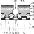
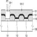
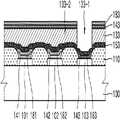
도 8은 본 발명의 제2 실시예에 따른 유기 발광 표시 장치(2)를 개략으로 도시한 단면도이고, 도 9는 본 발명의 제2 실시예에 따른 유기 발광 표시 장치의 일부를 도시한 평면도이다.8 is a schematic cross-sectional view of an organic light emitting
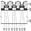
도 8 및 도 9를 참조하면, 기판(100) 상에 제1 애노드(101), 제2 애노드(102), 제3 애노드(103)를 포함하는 복수의 애노드가 서로 이격되어 배치된다. 제1 내지 제3 애노드(101, 102, 103) 상에는 제1 내지 제3 발광층을 포함하는 제1 내지 제3 유기 기능층(141, 142, 143)이 각각 위치하고, 제1 내지 제3 유기 기능층(141, 142, 143) 상에는 도전성 물질을 포함하는 제1 내지 제3 보조 캐소드(181, 182, 183)가 각각 위치한다. 제1 내지 제3 보조 캐소드(181, 182, 183) 상에는 일체로 형성된 공통 전극(180)이 위치한다.Referring to FIGS. 8 and 9 , a plurality of anodes including a
본 실시예에 따른 유기 발광 표시 장치(2)는 자기조립 단분자막(150)이 제1 내지 제3 애노드(101, 102, 103)의 주위를 둘러싸도록 위치하고, 자기조립 단분자막(150) 위로 화소 정의막(110)이 형성된다. 자기조립 단분자막(150)은 제1 내지 제3 애노드의 단부에서 소정 두께(D2) 만큼 중첩하도록 형성된다는 점에서 전술한 제1 실시예와 차이가 있다. 이하 전술한 제1 실시예와 동일한 내용에 대하여 설명을 생략할 수 있다.In the organic light emitting
도 10을 참조하면, 기판(100) 상에 제1 애노드(101), 제2 애노드(102) 및 제3 애노드(103)을 포함하는 복수의 애노드를 형성하고, 그 위에서 자기조립 단분자막(150)을 형성한다.Referring to FIG. 10, a plurality of anodes including a
도 11을 참조하면, 제1 애노드(101), 제2 애노드(102) 및 제3 애노드(103)의 가장자리를 둘러싸도록 화소 정의막(110)을 형성한다. 이때, 화소 정의막(110)의 단부는 자기조립 단분자막(150)의 단부와 중첩된다. 자기조립 단분자막(150)은 불소를 포함하는 작용기 및 가수분해가 가능한 반응기를 포함할 수 있다.Referring to FIG. 11 , a
도 12a를 참조하면, 도 11의 구조물 상에 제1 리프트오프층(121), 및 제1 포토레지스트(131)가 순차로 형성된다.Referring to FIG. 12A , a first lift-
제1 리프트오프층(121)은 불소 중합체를 포함하고, 제1 리프트오프층(121)은 도포법, 인쇄법, 증착법 등의 방법으로 형성할 수 있다. 제1 리프트오프층(121) 상에 제1 포토레지스트(131)를 형성한다. 광(L)을 투과시키는 영역(M11)을 포함하는 제1 포토마스크(M1)를 통하여 제1 애노드(101)에 대응되는 위치의 제1 포토레지스트(131)를 노광 시킨다.The first lift-
제1 리프트오프층(121)과 가까이 접하는 자기조립 단분자막(150)의 불소를 포함하는 작용기는, 제1 리프트오프층(121)에 대하여 표면 에너지의 차이가 작아, 자기조립 단분자막(150) 위에 리프트오프층(121)을 균일하게 형성할 수 있다.The fluorine-containing functional group of the self-assembled
도 12b를 참조하면, 제1 포토레지스트(131)를 현상(develop)한다. 현상된 제1 포토레지스트(131)는 제1 애노드(101)에 대응하는 위치인 제1 부분 (131-1)이 제거되고, 나머지 제2 부분(131-2)은 잔존한다.Referring to FIG. 12B , the
도 12c를 참조하면, 도 12b의 제1 포토레지스트(131)의 제1 영역(131-1) 패턴을 식각 마스크로 하여 제1 리프트오프층(121)을 에칭한다. 식각 공정에 의해, 제1 부분(131-1)에 대응하는 위치, 즉 제1 애노드(101) 상부에 형성된 제1 리프트오프층(121)이 식각된다. 제1 리프트오프층(121) 에칭 시, 불소를 포함하는 제1 용매는 제1 포토레지스트(131)의 제1 부분(131-1)의 경계면 아래에서 제1 언더컷 프로파일(UC1-1)을 형성한다.Referring to FIG. 12C , the first lift-
제1 리프트오프층(121)이 식각되는 동안 자기조립 단분자막(150)은 제1 애노드(101)의 상면에 잘 결합되어 있다.While the first lift-
도 12d를 참조하면, 도 12c의 구조물에 제1 플라즈마 열처리로 제1 애도느 상의 자기조립 단분자막(150)을 제거한다.Referring to FIG. 12D, the self-assembled
도 21에 도시된 바와 같이, 플라즈마 열처리에 의해 제1 애노드(101)와 자기조립 단분자막(150) 사이의 Si-O 결합이 깔끔하게 끊어진다.As shown in FIG. 21 , the Si—O bond between the
도 12e를 참조하면, 도 12d의 구조물 상에 제1 발광층(미도시)을 포함하는 제1 유기 기능층(141) 및 제1 보조 캐소드(181)를 순차로 형성한다. 제1 유기 기능층(141)의 일부는 제1 부분(131-1)에 대응하는 위치 즉 제1 애노드(101) 상부에 형성되고, 제1 유기 기능층(141)의 다른 부분은 제1 포토레지스트(131)의 제2 부분(131-2) 상에 형성된다. 제1 보조 캐소드(181)의 일부는 제1 유기 기능층(141)의 상면을 덮도록 형성되고, 제1 보조 캐소드(181)의 다른 일부는 제1 부분(131-1)을 제외한 제1 포토레지스트(131)의 나머지 영역인 제2 부분(131-2)에서 제1 유기 기능층(141) 위에 형성된다.Referring to FIG. 12E, a first organic
도 12f를 참조하면, 도 12e의 구조물에 대하여 리프트 오프 공정을 수행한다. 제1 포토레지스트(131)의 제2 부분(131-2, 도 12e) 하부에 형성된 제1 리프트오프층(121)을 리프트 오프 시킴으로써, 제1 포토레지스트(131)의 제2 부분(131-2, 도 12e) 위에 형성된 제1 유기 기능층(141) 및 제1 보조 캐소드(181)는 제거되고, 제1 애노드(101) 위에 형성된 제1 유기 기능층(141)과 제1 보조 캐소드(181)가 패턴으로 남는다.Referring to FIG. 12F, a lift-off process is performed on the structure of FIG. 12E. The second portion 131-2 of the
상술한 제1 단위 공정을 실시한 후, 제2 애노드(102)가 위치하는 영역에, 제1 유기 기능층(141)과 다른 색의 광을 방출하는 제2 유기 기능층(142)을 형성하는 제2 단위 공정을 실시한다. 이하, 도 13a 내지 도 13f를 참조하여 제2 단위 공정을 설명한다.After performing the above-described first unit process, the second organic
도 13a를 참조하면, 도 12의 구조물 상에 제2 리프트오프층(122), 및 제2 포토레지스트(132)가 순차로 형성된다. 광(L)을 투과시키는 영역(M21)을 포함하는 제2 포토마스크(M2)를 통하여 제2 애노드(102)에 대응되는 위치의 제2 포토레지스트(132)를 노광 시킨다.Referring to FIG. 13A , a second lift-
제2 리프트오프층(122)과 가까이 접하는 자기조립 단분자막(150)의 불소를 포함하는 작용기는, 제2 리프트오프층(122)에 대하여 표면 에너지의 차이가 작아, 자기조립 단분자막(150) 위에 제2 리프트오프층(122)을 균일하게 형성할 수 있다.The fluorine-containing functional group of the self-assembled
도 13b를 참조하면, 제2 포토레지스트(132)를 현상(develop)한다. 현상된 제2 포토레지스트(132)는 제2 애노드(102)에 대응하는 위치인 제1 부분 (132-1)이 제거되고, 나머지 제2 부분(132-2)은 잔존한다.Referring to FIG. 13B , the
도 13c를 참조하면, 도 13b의 제2 포토레지스트(132)의 제1 영역(132-1) 패턴을 식각 마스크로 하여 제2 리프트오프층(122)을 에칭한다. 식각 공정에 의해, 제1 부분(132-1)에 대응하는 위치, 즉 제2 애노드(102) 상부에 형성된 제2 리프트오프층(122)이 식각된다. 제2 리프트오프층(122) 에칭 시, 불소를 포함하는 제1 용매는 제2 포토레지스트(132)의 제1 부분(132-1)의 경계면 아래에서 제2 언더컷 프로파일(UC2-1)을 형성한다. 제2 리프트오프층(122)이 식각되는 동안 자기조립 단분자막(150)은 제2 애노드(102)의 상면에 잘 결합되어 있다.Referring to FIG. 13C , the second lift-
도 13d를 참조하면, 도 13c의 구조물에 제2 플라즈마 열처리(PT2)로 제2 애노드(102) 상의 자기조립 단분자막(150)을 제거한다. 플라즈마 열처리에 의해 제2 애노드(102)와 자기조립 단분자막(150) 사이의 Si-O 결합이 깔끔하게 끊어진다.Referring to FIG. 13D, the self-assembled
도 13e를 참조하면, 도 13d의 구조물 상에 제2 발광층(미도시)을 포함하는 제2 유기 기능층(142) 및 제2 보조 캐소드(182)를 순차로 형성한다. 제2 유기 기능층(142)의 일부는 제1 부분(132-1)에 대응하는 위치 즉 제2 애노드(102) 상부에 형성되고, 제2 유기 기능층(142)의 다른 부분은 제2 포토레지스트(132)의 제2 부분(132-2) 상에 형성된다. 제2 보조 캐소드(182)의 일부는 제2 유기 기능층(142)의 상면을 덮도록 형성되고, 제2 보조 캐소드(182)의 다른 일부는 제1 부분(132-1)을 제외한 제2 포토레지스트(132)의 나머지 영역인 제2 부분(132-2)에서 제2 유기 기능층(142) 위에 형성된다.Referring to FIG. 13E, a second organic
도 13f를 참조하면, 도 13e의 구조물에 대하여 리프트 오프 공정을 수행한다. 제2 포토레지스트(132)의 제2 부분(132-2) 하부에 형성된 제2 리프트오프층(122)을 리프트 오프 시킴으로써, 제2 포토레지스트(132)의 제2 부분(132-2) 위에 형성된 제2 유기 기능층(142) 및 제2 보조 캐소드(182)는 제거되고, 제2 애노드(102) 위에 형성된 제2 유기 기능층(142)과 제2 보조 캐소드(182)가 패턴으로 남는다.Referring to FIG. 13F, a lift-off process is performed on the structure of FIG. 13E. The second lift-
상술한 제2 단위 공정을 실시한 후, 제3 애노드(103)가 위치하는 영역에, 제1 및 제1 유기 기능층(141, 142)과 다른 색의 광을 방출하는 제3 유기 기능층(143)을 형성하는 제3 단위 공정을 실시한다. 이하, 도 14a 내지 도 14f를 참조하여 제3 단위 공정을 설명한다.After performing the above-described second unit process, the third organic
도 14a를 참조하면, 도 13f의 구조물 상에 제3 리프트오프층(123), 및 제3 포토레지스트(133)가 순차로 형성된다. 광(L)을 투과시키는 영역(M31)을 포함하는 제3 포토마스크(M3)를 통하여 제3 애노드(103)에 대응되는 위치의 제3 포토레지스트(133)를 노광 시킨다.Referring to FIG. 14A, a third lift-
제3 리프트오프층(123)과 가까이 접하는 자기조립 단분자막(150)의 불소를 포함하는 작용기는, 제3 리프트오프층(123)에 대하여 표면 에너지의 차이가 작아, 자기조립 단분자막(150) 위에 제3 리프트오프층(123)을 균일하게 형성할 수 있다.The fluorine-containing functional group of the self-assembled
도 14b를 참조하면, 제3 포토레지스트(133)를 현상(develop)한다. 현상된 제3 포토레지스트(133)는 제3 애노드(103)에 대응하는 위치인 제1 부분 (133-1)이 제거되고, 나머지 제3 부분(133-2)은 잔존한다.Referring to FIG. 14B , the
도 14c를 참조하면, 도 14b의 제3 포토레지스트(133)의 제1 영역(133-1) 패턴을 식각 마스크로 하여 제3 리프트오프층(123)을 에칭한다. 식각 공정에 의해, 제1 부분(133-1)에 대응하는 위치, 즉 제3 애노드(103) 상부에 형성된 제3 리프트오프층(123)이 식각된다. 제3 리프트오프층(123) 에칭 시, 불소를 포함하는 제1 용매는 제3 포토레지스트(133)의 제1 부분(133-1)의 경계면 아래에서 제3 언더컷 프로파일(UC3-1)을 형성한다. 제3 리프트오프층(123)이 식각되는 동안 자기조립 단분자막(150)은 제3 애노드(103)의 상면에 잘 결합되어 있다.Referring to FIG. 14C , the third lift-
도 14d를 참조하면, 도 14c의 구조물에 제3 플라즈마 열처리(PT3)로 제3 애노드(103) 상의 자기조립 단분자막(150)을 제거한다. 플라즈마 열처리에 의해 제3 애노드(103)와 자기조립 단분자막(150) 사이의 Si-O 결합이 깔끔하게 끊어진다.Referring to FIG. 14D, the self-assembled
도 14e를 참조하면, 도 14d의 구조물 상에 제3 발광층(미도시)을 포함하는 제3 유기 기능층(143) 및 제3 보조 캐소드(183)를 순차로 형성한다. 제3 유기 기능층(143)의 일부는 제1 부분(133-1)에 대응하는 위치 즉 제3 애노드(103) 상부에 형성되고, 제3 유기 기능층(143)의 다른 부분은 제3 포토레지스트(133)의 제2 부분(132-2) 상에 형성된다. 제3 보조 캐소드(183)의 일부는 제3 유기 기능층(143)의 상면을 덮도록 형성되고, 제3 보조 캐소드(183)의 다른 일부는 제1 부분(133-1)을 제외한 제3 포토레지스트(133)의 나머지 영역인 제3 부분(133-2)에서 제3 유기 기능층(143) 위에 형성된다.Referring to FIG. 14E , a third organic
도 14f를 참조하면, 도 14e의 구조물에 대하여 리프트 오프 공정을 수행한다. 제3 포토레지스트(133)의 제3 부분(133-2) 하부에 형성된 제3 리프트오프층(123)을 리프트 오프 시킴으로써, 제3 포토레지스트(133)의 제2 부분(133-2) 위에 형성된 제3 유기 기능층(143) 및 제3 보조 캐소드(183)는 제거되고, 제3 애노드(103) 위에 형성된 제3 유기 기능층(143)과 제3 보조 캐소드(183)가 패턴으로 남는다.Referring to FIG. 14F, a lift-off process is performed on the structure of FIG. 14E. The third lift-
이하, 도 15a 내지 도 17e를 참조하여 본 발명의 제3 실시예에 따른 유기 발광 표시 장치(3)의 제조 방법을 간략하게 설명한다.Hereinafter, a manufacturing method of the organic light emitting display device 3 according to the third exemplary embodiment of the present invention will be briefly described with reference to FIGS. 15A to 17E.
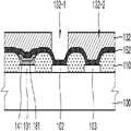
본 실시예는 제1 및 제2 실시예와 달리, 리프트오프층과 자기조립 단분자막(150)을 독립적으로 각각 사용하지 않고, 자기조립 단분자막(150)을 리프트오프층으로 사용하였다는 점에서 차이가 있다.Unlike the first and second embodiments, this embodiment is different in that the lift-off layer and the self-assembled
도 15a 내지 도 15e는 본 발명의 제3 실시예에 따른 유기 발광 표시 장치(3)의 제1 단위 공정을 개략적으로 도시한 단면도들이다.15A to 15E are cross-sectional views schematically illustrating a first unit process of an organic light emitting diode display 3 according to a third exemplary embodiment of the present invention.
도 15a를 참조하면, 기판(101) 상에 제1 내지 제3 애노드(101, 102, 103)를 형성하고, 제1 내지 제3 애노드(101, 102, 103)의 단부를 덮는 화소 정의막(110)을 형성한다. 화소 정의막(110)을 형성한 후, 제1 자기조립 단분자막(151)을 형성한다. 제1 자기 조립 단분자막(151) 상에 제1 포토레지스트(131)를 형성한다.Referring to FIG. 15A , first to
본 실시예의 제1 자기조립 단분자막(151)은 가수분해가 가능한 반응기와 불소를 포함하는 작용기를 포함할 수 있다. 한편, 본 실시예의 경우, 제1 자기조립 단분자막(151) 상부에는 제1 포토레지스트(131)가 형성된다. 제1 포토레지스트(131) 는 불소중합체를 포함할 수도 있지만, 반드시 그럴 필요는 없다. 따라서, 본 실시예의 제1 자기조립 단분자막(151)은 전술한 실시예와 같이 불소를 포함하는 작용기를 반드시 포함할 필요는 없다. 예를 들어, 제1 자기조립 단분자막(151)은 OTS(octadecyltrichlorosilane), DDMS(dichlorodimethylsilane), TEOS TetraEthOxySilane) 등을 더 포함할 수 있다.The first self-assembled
광(L)을 투과시키는 영역(M11)을 포함하는 제1 포토마스크(M1)를 통하여 제1 애노드(101)에 대응되는 위치의 제1 포토레지스트(131)를 노광 시킨다. 제1 포토레지스트층(131)과 가까이 접하는 제1 자기조립 단분자막(151)의 작용기는, 제1 포토레지스트(131)에 포함된 감광물질에 대하여 표면 에너지의 차이가 작은 물질을 사용할 수 있다.The
도 15b를 참조하면, 제1 포토레지스트(131)를 현상(develop)한다. 현상된 제1 포토레지스트(131)는 제1 애노드(101)에 대응하는 위치인 제1 부분 (131-1)이 제거되고, 나머지 제2 부분(131-2)은 잔존한다.Referring to FIG. 15B , the
도 15c를 참조하면, 도 15b의 구조물에 제1 플라즈마 열처리(PT1)로 제1 애노드(101) 상의 제1 자기조립 단분자막(151)을 제거한다. 제1 플라즈마 열처리(PT1)에 의해 제1 애노드(101)와 제1 자기조립 단분자막(151) 사이의 Si-O 결합이 깔끔하게 끊어진다.Referring to FIG. 15C , the first self-assembled
도 15d를 참조하면, 도 15c의 구조물 상에 제1 발광층(미도시)을 포함하는 제1 유기 기능층(141) 및 제1 보조 캐소드(181)를 순차로 형성한다. 제1 유기 기능층(141)의 일부는 제1 부분(131-1)에 대응하는 위치 즉 제1 애노드(101) 상부에 형성되고, 제1 유기 기능층(141)의 다른 부분은 제1 포토레지스트(131)의 제2 부분(132-2) 상에 형성된다. 제1 보조 캐소드(181)의 일부는 제1 유기 기능층(141)의 상면을 덮도록 형성되고, 제1 보조 캐소드(181)의 다른 일부는 제1 부분(131-1)을 제외한 제1 포토레지스트(131)의 나머지 영역인 제2 부분(131-2)에서 제1 유기 기능층(141) 위에 형성된다.Referring to FIG. 15D, a first organic
도 15e를 참조하면, 도 15d의 구조물에 대하여 리프트 오프 공정을 수행한다. 제1 포토레지스트(131)를 리프트 오프 시킴으로써, 제1 포토레지스트(131)의 제2 부분(131-2) 위에 형성된 제1 유기 기능층(141) 및 제1 보조 캐소드(181)는 제거되고, 제1 애노드(101) 위에 형성된 제1 유기 기능층(141)과 제1 보조 캐소드(181)가 패턴으로 남는다. 그리고, 화소 정의막(110)과 제1 포토레지스트(131) 사이에 위치하는 제1 자기조립 단분자막(151)도 함께 제거된다.Referring to FIG. 15E, a lift-off process is performed on the structure of FIG. 15D. By lifting off the
도 16a 내지 도 16e는 본 발명의 제3 실시예에 따른 유기 발광 표시 장치(3)의 제2 단위 공정을 개략적으로 도시한 단면도들이다.16A to 16E are cross-sectional views schematically illustrating a second unit process of an organic light emitting diode display 3 according to a third exemplary embodiment of the present invention.
도 16a를 참조하면, 도 15e의 구조물 상에 제2 자기조립 단분자막(152) 및 제2 포토레지스트(132)를 형성한다. 광(L)을 투과시키는 영역(M21)을 포함하는 제2 포토마스크(M2)를 통하여 제2 애노드(102)에 대응되는 위치의 제2 포토레지스트(132)를 노광 시킨다. 제2 포토레지스트층(132)과 가까이 접하는 제2 자기조립 단분자막(152)의 작용기는, 제2 포토레지스트(132)에 포함된 감광물질에 대하여 표면 에너지의 차이가 작은 물질을 사용할 수 있다.Referring to FIG. 16A, a second self-assembled
도 16b를 참조하면, 제2 포토레지스트(132)를 현상(develop)한다. 현상된 제2 포토레지스트(132)는 제2 애노드(102)에 대응하는 위치인 제2 부분 (132-1)이 제거되고, 나머지 제2 부분(132-2)은 잔존한다.Referring to FIG. 16B, the
도 16c를 참조하면, 도 16b의 구조물에 제2 플라즈마 열처리(PT2)로 제2 애노드(102) 상의 제2 자기조립 단분자막(152)을 제거한다. 제2 플라즈마 열처리(PT2)에 의해 제2 애노드(102)와 제2 자기조립 단분자막(152) 사이의 Si-O 결합이 깔끔하게 끊어진다.Referring to FIG. 16C , the second self-assembled
도 16d를 참조하면, 도 16c의 구조물 상에 제1 발광층(미도시)을 포함하는 제2 유기 기능층(142) 및 제2 보조 캐소드(182)를 순차로 형성한다. 제2 유기 기능층(142)의 일부는 제1 부분(132-1)에 대응하는 위치 즉 제2 애노드(102) 상부에 형성되고, 제2 유기 기능층(142)의 다른 부분은 제2 포토레지스트(132)의 제2 부분(132-2) 상에 형성된다. 제2 보조 캐소드(182)의 일부는 제2 유기 기능층(142)의 상면을 덮도록 형성되고, 제2 보조 캐소드(182)의 다른 일부는 제2 부분(132-1)을 제외한 제2 포토레지스트(132)의 나머지 영역인 제2 부분(132-2)에서 제2 유기 기능층(142) 위에 형성된다.Referring to FIG. 16D, a second organic
도 16e를 참조하면, 도 16d의 구조물에 대하여 리프트 오프 공정을 수행한다. 제2 포토레지스트(132)를 리프트 오프 시킴으로써, 제2 포토레지스트(132)의 제2 부분(132-2) 위에 형성된 제2 유기 기능층(142) 및 제2 보조 캐소드(182)는 제거되고, 제2 애노드(102) 위에 형성된 제2 유기 기능층(142)과 제2 보조 캐소드(182)가 패턴으로 남는다. 그리고, 화소 정의막(110)과 제2 포토레지스트(132) 사이에 위치하는 제2 자기조립 단분자막(152)도 함께 제거된다.Referring to FIG. 16E, a lift-off process is performed on the structure of FIG. 16D. By lifting off the
도 17a 내지 도 17e는 본 발명의 제3 실시예에 따른 유기 발광 표시 장치(3)의 제3 단위 공정을 개략적으로 도시한 단면도들로서, 제3 자기조립 단분자막(513)이 다시 형성되고 최종적으로는 모두 제거되는 것을 제외하고는 전술한 도 16a 내지 도 16e에서 설명한 내용과 유사하하므로 자세한 설명은 생략한다. .17A to 17E are cross-sectional views schematically illustrating a third unit process of an organic light emitting display device 3 according to a third embodiment of the present invention, in which a third self-assembled monolayer 513 is formed again and finally It is similar to the description of FIGS. 16A to 16E except that all of them are removed, so detailed descriptions are omitted. .
한편, 전술한 도면들에는 도시되지 않았으나, 전술한 유기 발광 표시 장치들는 유기 발광층을 봉지하는 봉지부재를 더 포함할 수 있다. 봉지 부재는 유리 기판, 금속 호일, 무기층과 유기층이 혼합된 박막 봉지층 등으로 형성될 수 있다.Meanwhile, although not shown in the drawings, the organic light emitting display devices described above may further include an encapsulation member for encapsulating the organic light emitting layer. The encapsulation member may be formed of a glass substrate, a metal foil, a thin film encapsulation layer in which an inorganic layer and an organic layer are mixed, or the like.
본 발명은 도면에 도시된 실시 예를 참고로 설명되었으나 이는 예시적인 것에 불과하며, 당해 기술 분야에서 통상의 지식을 가진 자라면 이로부터 다양한 변형 및 균등한 다른 실시 예가 가능하다는 점을 이해할 것이다. 따라서, 본 발명의 진정한 기술적 보호 범위는 첨부된 특허청구범위의 기술적 사상에 의하여 정해져야 할 것이다.Although the present invention has been described with reference to the embodiments shown in the drawings, this is merely exemplary, and those skilled in the art will understand that various modifications and equivalent other embodiments are possible therefrom. Therefore, the true technical scope of protection of the present invention should be determined by the technical spirit of the appended claims.
1: 유기 발광 표시 장치
100: 기판
101: 제1 애노드
102: 제2 애노드
103: 제3 애노드
110: 화소 정의막
121: 제1 리프트오프층
122: 제2 리프트오프층
123: 제3 리프트오프층
131: 제1 포토레지스트
132: 제2 포토레지스트
133: 제3 포토레지스트
141: 제1 유기 기능층
142: 제2 유기 기능층
143: 제3 유기 기능층
150: 자기조립 단분자막
181: 제1 보조 캐소드
182: 제2 보조 캐소드
183: 제3 보조 캐소드
180: 공통전극1: organic light emitting display device
100: substrate
101: first anode
102: second anode
103 third anode
110: pixel defining layer
121: first lift-off layer
122: second lift-off layer
123: third lift-off layer
131: first photoresist
132: second photoresist
133: third photoresist
141: first organic functional layer
142: second organic functional layer
143 third organic functional layer
150: self-assembled monolayer
181: first auxiliary cathode
182: second auxiliary cathode
183 third auxiliary cathode
180: common electrode
Claims (26)
Translated fromKorean상기 기판 위에 위치하는 제1 제1 전극;
상기 제1 제1 전극 위에 위치하고, 제1 발광층을 포함하는 제1 유기 기능층;
상기 제1 유기 기능층 위에 위치하는 제1 제2 전극;
상기 기판 위에 위치하고, 상기 제1 제1 전극과 이격되어 위치하는 제2 제1 전극;
상기 제2 제1 전극 위에 위치하고, 제2 발광층을 포함하는 제2 유기 기능층;
상기 제2 유기 기능층 위에 위치하는 제2 제2 전극;
상기 제1 유기 기능층과 상기 제2 유기 기능층 사이에 위치하고 불소를 함유한 자기조립 단분자막;
상기 제1 제2 전극 및 상기 제2 제2 전극 상에 일체로 공통으로 형성된 공통 전극; 및
상기 제1 제1 전극의 가장자리 및 상기 제2 제1 전극의 가장자리를 덮는, 절연층을 포함하는 화소 정의막;을 포함하며,
상기 자기조립 단분자막은 상기 공통 전극과 직접 접촉하고, 상기 제1 제2 전극 및 상기 제2 제2 전극 각각으로부터 이격되며,
상기 자기조립 단분자막과 상기 제1 제2 전극 사이, 및 상기 자기조립 단분자막과 상기 제2 제2 전극 사이에 있어서, 상기 공통 전극과 상기 화소 정의막이 접촉하는, 유기 발광 표시 장치.Board;
a first first electrode positioned on the substrate;
a first organic functional layer disposed on the first first electrode and including a first light emitting layer;
a first second electrode positioned on the first organic functional layer;
a second first electrode positioned on the substrate and spaced apart from the first first electrode;
a second organic functional layer disposed on the second first electrode and including a second light emitting layer;
a second second electrode positioned on the second organic functional layer;
a self-assembled monolayer disposed between the first organic functional layer and the second organic functional layer and containing fluorine;
a common electrode integrally and commonly formed on the first second electrode and the second second electrode; and
A pixel defining layer including an insulating layer covering edges of the first first electrode and edges of the second first electrode;
The self-assembled monolayer directly contacts the common electrode and is spaced apart from each of the first and second electrodes and the second second electrode,
The organic light emitting display device, wherein the common electrode and the pixel defining layer contact between the self-assembled monolayer and the first second electrode and between the self-assembled monolayer and the second electrode.
상기 제1 발광층에서 방출되는 색과 상기 제2 발광층에서 방출되는 색은 서로 다른 유기 발광 표시 장치.According to claim 1,
The organic light emitting display device of claim 1 , wherein a color emitted from the first light emitting layer and a color emitted from the second light emitting layer are different from each other.
상기 제1 유기 기능층 및 상기 제2 유기 기능층은 정공 주입층, 정공 수송층, 전자 수송층, 및 전자 주입층 중 적어도 하나의 기능층을 더 포함하는 유기 발광 표시 장치.According to claim 1,
The first organic functional layer and the second organic functional layer further include at least one functional layer of a hole injection layer, a hole transport layer, an electron transport layer, and an electron injection layer.
상기 제1 유기 기능층의 가장자리 및 상기 제2 유기 기능층의 가장자리는 상기 화소 정의막의 경사면에 위치하는 유기 발광 표시 장치.According to claim 1,
An edge of the first organic functional layer and an edge of the second organic functional layer are positioned on an inclined surface of the pixel defining layer.
상기 자기조립 단분자막은 상기 화소 정의막 상부에 위치하고, 상기 제1 유기 기능층 및 상기 제2 유기 기능층의 주위를 둘러싸도록 위치하는 유기 발광 표시 장치.According to claim 1,
The self-assembled monolayer is positioned on the pixel defining layer and positioned to surround the first organic functional layer and the second organic functional layer.
상기 기판 위에 위치하는 제1 제1 전극;
상기 제1 제1 전극 위에 위치하고, 제1 발광층을 포함하는 제1 유기 기능층;
상기 제1 유기 기능층 위에 위치하는 제1 제2 전극;
상기 기판 위에 위치하고, 상기 제1 제1 전극과 이격되어 위치하는 제2 제1 전극;
상기 제2 제1 전극 위에 위치하고, 제2 발광층을 포함하는 제2 유기 기능층;
상기 제2 유기 기능층 위에 위치하는 제2 제2 전극;
상기 제1 유기 기능층과 상기 제2 유기 기능층 사이에 위치하고 불소를 함유한 자기조립 단분자막;
상기 제1 제2 전극 및 상기 제2 제2 전극 상에 일체로 공통으로 형성된 공통 전극; 및
상기 제1 제1 전극의 가장자리 및 상기 제2 제1 전극의 가장자리를 덮는, 절연층을 포함하는 화소 정의막;을 포함하며,
상기 자기조립 단분자막은 상기 화소 정의막 상부에 위치하고 상기 공통 전극과 직접 접촉하며, 상기 제1 유기 기능층 및 상기 제2 유기 기능층의 주위를 둘러싸도록 배치되며,
상기 자기조립 단분자막은 상기 제1 유기 기능층 및 상기 제2 유기 기능층의 단부와 소정 간격 이격되어 위치하는 유기 발광 표시 장치.Board;
a first first electrode positioned on the substrate;
a first organic functional layer disposed on the first first electrode and including a first light emitting layer;
a first second electrode positioned on the first organic functional layer;
a second first electrode positioned on the substrate and spaced apart from the first first electrode;
a second organic functional layer disposed on the second first electrode and including a second light emitting layer;
a second second electrode positioned on the second organic functional layer;
a self-assembled monolayer disposed between the first organic functional layer and the second organic functional layer and containing fluorine;
a common electrode integrally and commonly formed on the first second electrode and the second second electrode; and
A pixel defining layer including an insulating layer covering edges of the first first electrode and edges of the second first electrode;
The self-assembled monolayer is disposed on the pixel-defining layer, directly contacts the common electrode, and surrounds the first organic functional layer and the second organic functional layer,
The organic light emitting display device of claim 1 , wherein the self-assembled monolayer is spaced apart from ends of the first organic functional layer and the second organic functional layer by a predetermined distance.
상기 기판 위에 위치하는 제1 제1 전극;
상기 제1 제1 전극 위에 위치하고, 제1 발광층을 포함하는 제1 유기 기능층;
상기 제1 유기 기능층 위에 위치하는 제1 제2 전극;
상기 기판 위에 위치하고, 상기 제1 제1 전극과 이격되어 위치하는 제2 제1 전극;
상기 제2 제1 전극 위에 위치하고, 제2 발광층을 포함하는 제2 유기 기능층;
상기 제2 유기 기능층 위에 위치하는 제2 제2 전극;
상기 제1 유기 기능층과 상기 제2 유기 기능층 사이에 위치하고 불소를 함유한 자기조립 단분자막; 및
상기 제1 제1 전극의 가장자리 및 상기 제2 제1 전극의 가장자리를 덮으며 절연층을 포함하는 화소 정의막;을 포함하며,
상기 자기조립 단분자막은 상기 화소 정의막 하부에 위치하고, 상기 제1 제1 전극 및 상기 제2 제1 전극의 주위를 둘러싸도록 위치하는 유기 발광 표시 장치.Board;
a first first electrode positioned on the substrate;
a first organic functional layer disposed on the first first electrode and including a first light emitting layer;
a first second electrode positioned on the first organic functional layer;
a second first electrode positioned on the substrate and spaced apart from the first first electrode;
a second organic functional layer disposed on the second first electrode and including a second light emitting layer;
a second second electrode positioned on the second organic functional layer;
a self-assembled monolayer disposed between the first organic functional layer and the second organic functional layer and containing fluorine; and
a pixel defining layer covering an edge of the first electrode and an edge of the second electrode and including an insulating layer;
The organic light emitting display device of claim 1 , wherein the self-assembled monolayer is positioned under the pixel defining layer and surrounds the first electrode and the second electrode.
상기 자기조립 단분자막은 제1 제1 전극 및 상기 제2 제1 전극의 단부에서 상기 제1 제1 전극 및 상기 제2 제1 전극과 중첩하는 유기 발광 표시 장치.According to claim 8,
The self-assembled monolayer overlaps the first first electrode and the second first electrode at ends of the first first electrode and the second first electrode.
상기 자기조립 단분자막은, 불화카본기(-CF3)를 포함하는 유기 발광 표시 장치.According to claim 1,
The organic light emitting display device of claim 1 , wherein the self-assembled monolayer includes a fluorocarbon group (-CF3).
상기 제1 제1 전극 및 제2 제1 전극은 도전성 산화물을 포함하는 유기 발광 표시 장치.According to claim 1,
The first electrode and the second first electrode include a conductive oxide.
상기 제1 제1 전극 및 제2 제1 전극은 인듐틴옥사이드 (indium tin oxide), 인듐징크옥사이드 (indium zinc oxide), 징크옥사이드 (zinc oxide), 인듐옥사이드 (indium oxide), 인듐갈륨옥사이드 (indium gallium oxide), 및 알루미늄징크옥사이드 (aluminum zinc oxide:)에서 선택된 유기 발광 표시 장치.According to claim 11,
The first first electrode and the second first electrode may be made of indium tin oxide, indium zinc oxide, zinc oxide, indium oxide, or indium gallium oxide. An organic light emitting display device selected from gallium oxide, and aluminum zinc oxide.
상기 제1 제1 전극 및 제2 제1전극 상에, 불소를 함유하는 자기조립 단분자막을 형성함;
상기 자기조립 단분자막 상에 제1 리프트오프층 및 제1 포토레지스트를 순차로 형성함;
상기 제1 제1 전극에 대응되는 영역에 상기 제1 리프트오프층 및 상기 제1 포토레지스트를 제거하고, 상기 자기조립 단분자막을 잔존시킴:
제1 플라즈마 열처리로 상기 제1 제1 전극 상의 자기조립 단분자막을 제거함; 및
상기 제1 제1 전극 상에 제1 발광층을 포함하는 제1 유기 기능층 및 제1 제2 전극을 순차로 형성하고, 상기 제1 리프트오프층의 나머지 부분을 리프트오프 시킴;을 포함하는 유기 전계 발광 표시 장치의 제조 방법.forming a first first electrode and a second first electrode spaced apart from each other on the substrate;
forming a self-assembled monolayer containing fluorine on the first electrode and the second electrode;
sequentially forming a first lift-off layer and a first photoresist on the self-assembled monolayer;
removing the first lift-off layer and the first photoresist in a region corresponding to the first electrode, and leaving the self-assembled monolayer:
removing the self-assembled monolayer on the first electrode by a first plasma heat treatment; and
sequentially forming a first organic functional layer including a first light emitting layer and a first second electrode on the first electrode, and lifting off the remaining portion of the first lift-off layer; A method of manufacturing a light emitting display device.
상기 제1 리프트오프층은 불소 함량이 20~60 wt%인 유기 발광 표시 장치의 제조 방법.According to claim 14,
The method of claim 1 , wherein the first lift-off layer has a fluorine content of 20 to 60 wt%.
상기 제1 유기 기능층 및 상기 제1 제2 전극은 증착 공정으로 형성하는 유기 발광 표시 장치의 제조 방법.According to claim 14,
The method of manufacturing an organic light emitting display device in which the first organic functional layer and the first and second electrodes are formed through a deposition process.
상기 제1 포토레지스트의 일부를 제거하는 패터닝하는 공정은 포토리쏘그라피 공정으로 형성하는 유기 발광 표시 장치의 제조 방법.According to claim 14,
The patterning process of removing a portion of the first photoresist is a method of manufacturing an organic light emitting display device formed by a photolithography process.
상기 제1 리프트오프층은 불소를 포함하는 제1 용매로 에칭하여 제거하는 유기 발광 표시 장치의 제조 방법.According to claim 14,
The method of claim 1 , wherein the first lift-off layer is removed by etching with a first solvent containing fluorine.
상기 자기조립 단분자막은 증기증착법(vapor deposition method)으로 형성하는 유기 발광 표시 장치의 제조 방법.According to claim 14,
The method of manufacturing an organic light emitting display device in which the self-assembled monolayer is formed by a vapor deposition method.
상기 자기조립 단분자막은, 가수분해 가능한 반응기; 및 함불소 작용기를 포함하도록 형성하는 유기 발광 표시 장치의 제조 방법.According to claim 14,
The self-assembled monolayer may include a hydrolyzable reactive group; and a method of manufacturing an organic light emitting display device comprising a fluorine-containing functional group.
상기 제1 리프트오프층의 나머지 부분을 리프트오프 시킨 후, 제2 리프트오프층 및 제2 포토레지스트를 순차로 형성함;
상기 제2 제1 전극에 대응되는 영역에 상기 제2 리프트오프층 및 상기 제2 포토레지스트를 제거하고, 상기 자기조립 단분자막을 잔존시킴:
제2 플라즈마 열처리로 상기 제2 제1 전극 상의 자기조립 단분자막을 제거함;
상기 제2 제1 전극 상에 제2 발광층을 포함하는 제2 유기 기능층 및 제2 제2 전극을 순차로 형성하고, 상기 제2 리프트오프층의 나머지 부분을 리프트오프 시킴;을 더 포함하는 유기 발광 표시 장치의 제조 방법.According to claim 14,
After lifting off the remaining portion of the first lift-off layer, sequentially forming a second lift-off layer and a second photoresist;
removing the second lift-off layer and the second photoresist in a region corresponding to the second first electrode, and leaving the self-assembled monolayer:
removing the self-assembled monolayer on the second first electrode by a second plasma heat treatment;
sequentially forming a second organic functional layer including a second light emitting layer and a second second electrode on the second first electrode, and lifting off the remaining portion of the second lift-off layer; A method of manufacturing a light emitting display device.
상기 제1 제1 전극과 상기 제2 제1전극 사이에 절연층을 포함하는 화소 정의막을 더 형성하는 유기 발광 표시 장치의 제조 방법.According to claim 14,
The method of manufacturing the organic light emitting display device further forming a pixel defining layer including an insulating layer between the first first electrode and the second first electrode.
상기 자기조립 단분자막은 상기 화소 정의막 상부에 형성하는 유기 발광 표시 장치의 제조 방법.23. The method of claim 22,
The method of manufacturing an organic light emitting display device in which the self-assembled monolayer is formed on the pixel defining layer.
상기 자기조립 단분자막은 상기 화소 정의막 하부에 형성하는 유기 발광 표시 장치의 제조 방법.23. The method of claim 22,
The method of manufacturing an organic light emitting display device in which the self-assembled monolayer is formed under the pixel defining layer.
상기 제1 제2 전극 및 상기 제2 제2전극 상에 공통으로 일체의 형상으로 위치하는 공통 전극을 더 형성하는 유기 발광 표시 장치의 제조 방법.According to claim 21,
The method of manufacturing the organic light emitting display device further forming a common electrode integrally positioned on the first and second electrodes and the second electrode.
상기 제1 제1 전극 및 제2 제1전극 상에, 제1 자기조립 단분자막을 형성함;
상기 제1 자기조립 단분자막 상에 제1 포토레지스트를 형성함;
상기 제1 제1 전극에 대응되는 영역에 상기 제1 포토레지스트를 제거하고, 상기 제1 자기조립 단분자막을 잔존시킴:
제1 플라즈마 열처리로 상기 제1 제1 전극 상의 제1 자기조립 단분자막을 제거함; 및
상기 제1 제1 전극 상에 제1 발광층을 포함하는 제1 유기 기능층 및 제1 제2 전극을 순차로 형성하고, 상기 제1 포토레지스트 및 제1 자기조립 단분자막의 나머지 부분을 리프트오프 시킴;을 포함하는 유기 전계 발광 표시 장치의 제조 방법.forming a first first electrode and a second first electrode spaced apart from each other on the substrate;
forming a first self-assembled monolayer on the first electrode and the second electrode;
forming a first photoresist on the first self-assembled monolayer;
removing the first photoresist from a region corresponding to the first electrode, and leaving the first self-assembled monolayer;
removing the first self-assembled monolayer on the first electrode by a first plasma heat treatment; and
sequentially forming a first organic functional layer including a first light emitting layer and a first second electrode on the first electrode, and lifting off remaining portions of the first photoresist and the first self-assembled monolayer; A method of manufacturing an organic electroluminescent display device comprising a.
Priority Applications (12)
| Application Number | Priority Date | Filing Date | Title |
|---|---|---|---|
| KR1020170030982AKR102482456B1 (en) | 2017-03-13 | 2017-03-13 | Organic light-emitting apparatus and the method for manufacturing of the organic light-emitting display apparatus |
| US15/907,430US10658438B2 (en) | 2017-03-13 | 2018-02-28 | Organic light-emitting display apparatus comprising self-assembled layer containing fluorine and method of manufacturing the same |
| CN201810192912.1ACN108573996B (en) | 2017-03-13 | 2018-03-09 | Organic light emitting display device and method of manufacturing the same |
| EP18161103.9AEP3376550B1 (en) | 2017-03-13 | 2018-03-09 | Organic light-emitting display apparatus and method of manufacturing the same |
| CN202310911504.8ACN116887629A (en) | 2017-03-13 | 2018-03-09 | Organic light-emitting display device and method of manufacturing organic light-emitting display device |
| TW111133052ATWI816536B (en) | 2017-03-13 | 2018-03-12 | Organic light-emitting display apparatus and method of manufacturing the same |
| TW107108337ATWI779017B (en) | 2017-03-13 | 2018-03-12 | Organic light-emitting display apparatus and method of manufacturing the same |
| JP2018044295AJP7123465B2 (en) | 2017-03-13 | 2018-03-12 | Organic light-emitting display device and method for manufacturing organic light-emitting display device |
| US16/852,291US11164924B2 (en) | 2017-03-13 | 2020-04-17 | Organic light-emitting display apparatus comprising self-assembled layer containing fluorine |
| US17/481,002US11758768B2 (en) | 2017-03-13 | 2021-09-21 | Organic light-emitting display apparatus comprising self-assembled layer containing fluorine |
| JP2022096069AJP7331206B2 (en) | 2017-03-13 | 2022-06-14 | organic light emitting display |
| KR1020220183490AKR102700938B1 (en) | 2017-03-13 | 2022-12-23 | Organic light-emitting apparatus and the method for manufacturing of the organic light-emitting display apparatus |
Applications Claiming Priority (1)
| Application Number | Priority Date | Filing Date | Title |
|---|---|---|---|
| KR1020170030982AKR102482456B1 (en) | 2017-03-13 | 2017-03-13 | Organic light-emitting apparatus and the method for manufacturing of the organic light-emitting display apparatus |
Related Child Applications (1)
| Application Number | Title | Priority Date | Filing Date |
|---|---|---|---|
| KR1020220183490ADivisionKR102700938B1 (en) | 2017-03-13 | 2022-12-23 | Organic light-emitting apparatus and the method for manufacturing of the organic light-emitting display apparatus |
Publications (2)
| Publication Number | Publication Date |
|---|---|
| KR20180104784A KR20180104784A (en) | 2018-09-27 |
| KR102482456B1true KR102482456B1 (en) | 2022-12-29 |
Family
ID=61622425
Family Applications (2)
| Application Number | Title | Priority Date | Filing Date |
|---|---|---|---|
| KR1020170030982AActiveKR102482456B1 (en) | 2017-03-13 | 2017-03-13 | Organic light-emitting apparatus and the method for manufacturing of the organic light-emitting display apparatus |
| KR1020220183490AActiveKR102700938B1 (en) | 2017-03-13 | 2022-12-23 | Organic light-emitting apparatus and the method for manufacturing of the organic light-emitting display apparatus |
Family Applications After (1)
| Application Number | Title | Priority Date | Filing Date |
|---|---|---|---|
| KR1020220183490AActiveKR102700938B1 (en) | 2017-03-13 | 2022-12-23 | Organic light-emitting apparatus and the method for manufacturing of the organic light-emitting display apparatus |
Country Status (6)
| Country | Link |
|---|---|
| US (3) | US10658438B2 (en) |
| EP (1) | EP3376550B1 (en) |
| JP (2) | JP7123465B2 (en) |
| KR (2) | KR102482456B1 (en) |
| CN (2) | CN108573996B (en) |
| TW (2) | TWI816536B (en) |
Families Citing this family (14)
| Publication number | Priority date | Publication date | Assignee | Title |
|---|---|---|---|---|
| KR102482456B1 (en)* | 2017-03-13 | 2022-12-29 | 삼성디스플레이 주식회사 | Organic light-emitting apparatus and the method for manufacturing of the organic light-emitting display apparatus |
| US10700299B2 (en)* | 2017-08-01 | 2020-06-30 | Zixu Optronics Technology (Shanghai) Limited | Method for manufacturing organic light emitting diode using conductive protective layer |
| KR102614588B1 (en)* | 2018-08-20 | 2023-12-18 | 삼성디스플레이 주식회사 | Method of manufacturing display apparatus |
| US20220020830A1 (en)* | 2018-11-19 | 2022-01-20 | Dinguo Chen | Patterning of Organic Light Emitting Diode Device and the OLED Displays Manufactured Therefrom |
| US11145844B2 (en)* | 2019-02-27 | 2021-10-12 | Int Tech Co., Ltd. | Method for manufacturing electroluminescent device |
| US11374183B2 (en) | 2019-04-01 | 2022-06-28 | Samsung Display Co., Ltd. | Method of manufacturing display device |
| KR102830385B1 (en) | 2019-06-28 | 2025-07-07 | 삼성디스플레이 주식회사 | Display apparatus and manufacturing method thereof |
| CN111180498B (en)* | 2020-01-06 | 2022-06-03 | 京东方科技集团股份有限公司 | Display substrate, electroluminescent display panel and preparation method thereof |
| CN112349865B (en)* | 2020-10-26 | 2024-04-26 | 京东方科技集团股份有限公司 | OLED panel manufacturing method, OLED panel and electronic equipment |
| CN115918298A (en)* | 2020-12-16 | 2023-04-04 | 京东方科技集团股份有限公司 | Methods for patterning quantum dot layers |
| CN116601692A (en)* | 2020-12-22 | 2023-08-15 | 夏普株式会社 | Manufacturing method of display device and display device |
| US20250048833A1 (en)* | 2021-11-05 | 2025-02-06 | Sharp Kabushiki Kaisha | Method for manufacturing display device, and display device |
| US20240334722A1 (en)* | 2021-11-24 | 2024-10-03 | Sharp Display Technology Corporation | Display device and method for manufacturing display device |
| TWI790168B (en)* | 2022-05-11 | 2023-01-11 | 天光材料科技股份有限公司 | Method of patterning semiconductor layer |
Citations (1)
| Publication number | Priority date | Publication date | Assignee | Title |
|---|---|---|---|---|
| WO2016019273A1 (en) | 2014-08-01 | 2016-02-04 | Orthogonal, Inc. | Photolithographic patterning of organic electronic devices |
Family Cites Families (25)
| Publication number | Priority date | Publication date | Assignee | Title |
|---|---|---|---|---|
| TW490997B (en) | 2000-03-31 | 2002-06-11 | Seiko Epson Corp | Method of manufacturing organic EL element, and organic EL element |
| JP2002237383A (en) | 2000-03-31 | 2002-08-23 | Seiko Epson Corp | Method of manufacturing organic EL element, organic EL element |
| JP2002170669A (en) | 2000-12-01 | 2002-06-14 | Tdk Corp | Organic EL display device and manufacturing method thereof |
| US6975067B2 (en) | 2002-12-19 | 2005-12-13 | 3M Innovative Properties Company | Organic electroluminescent device and encapsulation method |
| WO2007063814A1 (en)* | 2005-12-02 | 2007-06-07 | Semiconductor Energy Laboratory Co., Ltd. | Semiconductor device, display device, and electronic device |
| JP2007157662A (en)* | 2005-12-08 | 2007-06-21 | Seiko Epson Corp | Organic light emitting device manufacturing method, organic light emitting device, and electronic apparatus |
| KR100753224B1 (en)* | 2005-12-30 | 2007-08-30 | (재)대구경북과학기술연구원 | Backplane for electroluminescent device and electroluminescent device comprising same |
| KR100841170B1 (en) | 2007-04-26 | 2008-06-24 | 삼성전자주식회사 | Low resistance metal wiring method, metal wiring structure and display device using same |
| WO2009126916A2 (en) | 2008-04-10 | 2009-10-15 | The Johns Hopkins University | Patterning devices using fluorinated compounds |
| WO2010038356A1 (en) | 2008-09-30 | 2010-04-08 | パナソニック株式会社 | Organic el device and method for manufacturing same |
| JP4844767B2 (en) | 2008-10-03 | 2011-12-28 | ソニー株式会社 | THIN FILM TRANSISTOR, METHOD FOR PRODUCING THIN FILM TRANSISTOR, AND ELECTRONIC DEVICE |
| KR101144915B1 (en) | 2008-12-08 | 2012-05-16 | 광주과학기술원 | Method for forming of pattern using self-assembled monolayer |
| JP4755314B2 (en) | 2009-03-06 | 2011-08-24 | パナソニック株式会社 | Organic EL display panel and manufacturing method thereof |
| JP5447996B2 (en)* | 2011-10-14 | 2014-03-19 | ソニー株式会社 | THIN FILM TRANSISTOR, METHOD FOR PRODUCING THIN FILM TRANSISTOR, AND ELECTRONIC DEVICE |
| KR101950838B1 (en)* | 2012-07-30 | 2019-02-21 | 엘지디스플레이 주식회사 | Method of fabricating the organic light emitting diode display device |
| JP2014123441A (en)* | 2012-12-20 | 2014-07-03 | Canon Inc | Method for manufacturing organic el display device |
| KR101976829B1 (en) | 2012-12-21 | 2019-05-13 | 엘지디스플레이 주식회사 | Large Area Organic Light Emitting Diode Display And Method For Manufacturing The Same |
| KR102205700B1 (en)* | 2014-07-16 | 2021-01-21 | 삼성전자주식회사 | Organic electro-luminescent display and method of fabricating the same |
| KR102552276B1 (en) | 2015-02-24 | 2023-07-07 | 삼성디스플레이 주식회사 | Organic light emitting display device and manufacturing method of the same |
| KR102360093B1 (en)* | 2015-07-22 | 2022-02-09 | 삼성디스플레이 주식회사 | Organic light-emitting display apparatus and the method for manufacturing of the organic light-emitting display apparatus |
| KR102313365B1 (en)* | 2015-08-25 | 2021-10-18 | 삼성디스플레이 주식회사 | Method for manufacturing of organic light-emitting display apparatus |
| JP2017091802A (en)* | 2015-11-10 | 2017-05-25 | 株式会社Joled | Organic el display panel and method of manufacturing organic el display panel |
| KR102629936B1 (en)* | 2016-07-29 | 2024-01-29 | 삼성디스플레이 주식회사 | Organic light-emitting apparatus and the method for manufacturing of the organic light-emitting display apparatus |
| KR102603867B1 (en)* | 2016-08-01 | 2023-11-21 | 삼성디스플레이 주식회사 | Organic light-emitting apparatus and the method for manufacturing of the organic light-emitting display apparatus |
| KR102482456B1 (en) | 2017-03-13 | 2022-12-29 | 삼성디스플레이 주식회사 | Organic light-emitting apparatus and the method for manufacturing of the organic light-emitting display apparatus |
- 2017
- 2017-03-13KRKR1020170030982Apatent/KR102482456B1/enactiveActive
- 2018
- 2018-02-28USUS15/907,430patent/US10658438B2/enactiveActive
- 2018-03-09CNCN201810192912.1Apatent/CN108573996B/enactiveActive
- 2018-03-09EPEP18161103.9Apatent/EP3376550B1/enactiveActive
- 2018-03-09CNCN202310911504.8Apatent/CN116887629A/enactivePending
- 2018-03-12JPJP2018044295Apatent/JP7123465B2/enactiveActive
- 2018-03-12TWTW111133052Apatent/TWI816536B/enactive
- 2018-03-12TWTW107108337Apatent/TWI779017B/enactive
- 2020
- 2020-04-17USUS16/852,291patent/US11164924B2/enactiveActive
- 2021
- 2021-09-21USUS17/481,002patent/US11758768B2/enactiveActive
- 2022
- 2022-06-14JPJP2022096069Apatent/JP7331206B2/enactiveActive
- 2022-12-23KRKR1020220183490Apatent/KR102700938B1/enactiveActive
Patent Citations (1)
| Publication number | Priority date | Publication date | Assignee | Title |
|---|---|---|---|---|
| WO2016019273A1 (en) | 2014-08-01 | 2016-02-04 | Orthogonal, Inc. | Photolithographic patterning of organic electronic devices |
Also Published As
| Publication number | Publication date |
|---|---|
| CN108573996A (en) | 2018-09-25 |
| EP3376550B1 (en) | 2019-12-25 |
| US20200243624A1 (en) | 2020-07-30 |
| KR102700938B1 (en) | 2024-09-02 |
| US20220005895A1 (en) | 2022-01-06 |
| JP2018152339A (en) | 2018-09-27 |
| TW202304038A (en) | 2023-01-16 |
| JP7123465B2 (en) | 2022-08-23 |
| US11758768B2 (en) | 2023-09-12 |
| CN108573996B (en) | 2023-08-11 |
| KR20230008660A (en) | 2023-01-16 |
| US20180261656A1 (en) | 2018-09-13 |
| US11164924B2 (en) | 2021-11-02 |
| JP2022126730A (en) | 2022-08-30 |
| US10658438B2 (en) | 2020-05-19 |
| TW201842691A (en) | 2018-12-01 |
| CN116887629A (en) | 2023-10-13 |
| KR20180104784A (en) | 2018-09-27 |
| EP3376550A1 (en) | 2018-09-19 |
| JP7331206B2 (en) | 2023-08-22 |
| TWI816536B (en) | 2023-09-21 |
| TWI779017B (en) | 2022-10-01 |
Similar Documents
| Publication | Publication Date | Title |
|---|---|---|
| KR102482456B1 (en) | Organic light-emitting apparatus and the method for manufacturing of the organic light-emitting display apparatus | |
| KR102775869B1 (en) | Organic light-emitting apparatus and the method for manufacturing of the organic light-emitting display apparatus | |
| KR102660896B1 (en) | Organic light-emitting apparatus and the method for manufacturing of the organic light-emitting display apparatus | |
| KR102603867B1 (en) | Organic light-emitting apparatus and the method for manufacturing of the organic light-emitting display apparatus | |
| US11469374B2 (en) | Organic light-emitting display apparatus and method of manufacturing the same | |
| CN104659287B (en) | Pixel defining layer and preparation method, display base plate and preparation method, display device | |
| CN107689390B (en) | Pixel defining layer and method for manufacturing the same, display substrate, and display panel | |
| KR102602193B1 (en) | Organic light-emitting apparatus and the method for manufacturing of the organic light-emitting display apparatus | |
| KR102278608B1 (en) | Organic light-emitting apparatus and the method for manufacturing of the organic light-emitting display apparatus | |
| KR20230052951A (en) | Metal overhang for advanced patterning | |
| KR102671037B1 (en) | Organic light emitting display apparatus and method of manufacturing the same | |
| KR102679420B1 (en) | Organic light emitting display apparatus and method of manufacturing the same | |
| CN1689377B (en) | Method for manufacturing light emitting display | |
| KR20070050786A (en) | OLED device and manufacturing method |
Legal Events
| Date | Code | Title | Description |
|---|---|---|---|
| PA0109 | Patent application | St.27 status event code:A-0-1-A10-A12-nap-PA0109 | |
| PG1501 | Laying open of application | St.27 status event code:A-1-1-Q10-Q12-nap-PG1501 | |
| R18-X000 | Changes to party contact information recorded | St.27 status event code:A-3-3-R10-R18-oth-X000 | |
| A201 | Request for examination | ||
| PA0201 | Request for examination | St.27 status event code:A-1-2-D10-D11-exm-PA0201 | |
| E902 | Notification of reason for refusal | ||
| PE0902 | Notice of grounds for rejection | St.27 status event code:A-1-2-D10-D21-exm-PE0902 | |
| AMND | Amendment | ||
| P11-X000 | Amendment of application requested | St.27 status event code:A-2-2-P10-P11-nap-X000 | |
| P13-X000 | Application amended | St.27 status event code:A-2-2-P10-P13-nap-X000 | |
| E601 | Decision to refuse application | ||
| PE0601 | Decision on rejection of patent | St.27 status event code:N-2-6-B10-B15-exm-PE0601 | |
| X091 | Application refused [patent] | ||
| E13-X000 | Pre-grant limitation requested | St.27 status event code:A-2-3-E10-E13-lim-X000 | |
| P11-X000 | Amendment of application requested | St.27 status event code:A-2-2-P10-P11-nap-X000 | |
| P13-X000 | Application amended | St.27 status event code:A-2-2-P10-P13-nap-X000 | |
| PX0901 | Re-examination | St.27 status event code:A-2-3-E10-E12-rex-PX0901 | |
| PX0701 | Decision of registration after re-examination | St.27 status event code:A-3-4-F10-F13-rex-PX0701 | |
| PA0107 | Divisional application | St.27 status event code:A-0-1-A10-A18-div-PA0107 St.27 status event code:A-0-1-A10-A16-div-PA0107 | |
| PR0701 | Registration of establishment | St.27 status event code:A-2-4-F10-F11-exm-PR0701 | |
| PR1002 | Payment of registration fee | St.27 status event code:A-2-2-U10-U11-oth-PR1002 Fee payment year number:1 | |
| PG1601 | Publication of registration | St.27 status event code:A-4-4-Q10-Q13-nap-PG1601 | |
| P22-X000 | Classification modified | St.27 status event code:A-4-4-P10-P22-nap-X000 | |
| P22-X000 | Classification modified | St.27 status event code:A-4-4-P10-P22-nap-X000 |