KR102481166B1 - Method of post-etching - Google Patents
Method of post-etchingDownload PDFInfo
- Publication number
- KR102481166B1 KR102481166B1KR1020150152006AKR20150152006AKR102481166B1KR 102481166 B1KR102481166 B1KR 102481166B1KR 1020150152006 AKR1020150152006 AKR 1020150152006AKR 20150152006 AKR20150152006 AKR 20150152006AKR 102481166 B1KR102481166 B1KR 102481166B1
- Authority
- KR
- South Korea
- Prior art keywords
- post
- plasma
- damaged
- region
- etching
- Prior art date
- Legal status (The legal status is an assumption and is not a legal conclusion. Google has not performed a legal analysis and makes no representation as to the accuracy of the status listed.)
- Active
Links
- 238000000034methodMethods0.000titleclaimsabstractdescription183
- 238000005530etchingMethods0.000titleclaimsabstractdescription89
- 238000012805post-processingMethods0.000claimsabstractdescription80
- 238000001020plasma etchingMethods0.000claimsabstractdescription18
- 239000007789gasSubstances0.000claimsdescription82
- 238000004140cleaningMethods0.000claimsdescription25
- 150000002500ionsChemical class0.000claimsdescription25
- 239000011261inert gasSubstances0.000claimsdescription10
- 238000005108dry cleaningMethods0.000claimsdescription5
- 238000011065in-situ storageMethods0.000claimsdescription4
- 238000003672processing methodMethods0.000claimsdescription4
- 239000004065semiconductorSubstances0.000abstractdescription20
- 238000004519manufacturing processMethods0.000abstractdescription6
- 239000010408filmSubstances0.000description49
- 239000000460chlorineSubstances0.000description22
- OKTJSMMVPCPJKN-UHFFFAOYSA-NCarbonChemical compound[C]OKTJSMMVPCPJKN-UHFFFAOYSA-N0.000description9
- 229910052799carbonInorganic materials0.000description9
- 230000000052comparative effectEffects0.000description8
- 239000000356contaminantSubstances0.000description8
- 239000000758substrateSubstances0.000description8
- XUIMIQQOPSSXEZ-UHFFFAOYSA-NSiliconChemical compound[Si]XUIMIQQOPSSXEZ-UHFFFAOYSA-N0.000description4
- 238000004380ashingMethods0.000description4
- 210000004087corneaAnatomy0.000description4
- 229910052710siliconInorganic materials0.000description4
- 239000010703siliconSubstances0.000description4
- 229910052581Si3N4Inorganic materials0.000description3
- 239000006227byproductSubstances0.000description3
- 239000000463materialSubstances0.000description3
- HQVNEWCFYHHQES-UHFFFAOYSA-Nsilicon nitrideChemical compoundN12[Si]34N5[Si]62N3[Si]51N64HQVNEWCFYHHQES-UHFFFAOYSA-N0.000description3
- XKRFYHLGVUSROY-UHFFFAOYSA-NArgonChemical compound[Ar]XKRFYHLGVUSROY-UHFFFAOYSA-N0.000description2
- ZAMOUSCENKQFHK-UHFFFAOYSA-NChlorine atomChemical compound[Cl]ZAMOUSCENKQFHK-UHFFFAOYSA-N0.000description2
- PXGOKWXKJXAPGV-UHFFFAOYSA-NFluorineChemical compoundFFPXGOKWXKJXAPGV-UHFFFAOYSA-N0.000description2
- VYPSYNLAJGMNEJ-UHFFFAOYSA-NSilicium dioxideChemical compoundO=[Si]=OVYPSYNLAJGMNEJ-UHFFFAOYSA-N0.000description2
- RTAQQCXQSZGOHL-UHFFFAOYSA-NTitaniumChemical compound[Ti]RTAQQCXQSZGOHL-UHFFFAOYSA-N0.000description2
- NRTOMJZYCJJWKI-UHFFFAOYSA-NTitanium nitrideChemical compound[Ti]#NNRTOMJZYCJJWKI-UHFFFAOYSA-N0.000description2
- XAGFODPZIPBFFR-UHFFFAOYSA-NaluminiumChemical compound[Al]XAGFODPZIPBFFR-UHFFFAOYSA-N0.000description2
- 229910052782aluminiumInorganic materials0.000description2
- 229910052801chlorineInorganic materials0.000description2
- 230000008878couplingEffects0.000description2
- 238000010168coupling processMethods0.000description2
- 238000005859coupling reactionMethods0.000description2
- 230000007547defectEffects0.000description2
- 230000006866deteriorationEffects0.000description2
- 230000005684electric fieldEffects0.000description2
- 229910052731fluorineInorganic materials0.000description2
- 239000011737fluorineSubstances0.000description2
- 229910052732germaniumInorganic materials0.000description2
- GNPVGFCGXDBREM-UHFFFAOYSA-Ngermanium atomChemical compound[Ge]GNPVGFCGXDBREM-UHFFFAOYSA-N0.000description2
- 238000009413insulationMethods0.000description2
- 229910021420polycrystalline siliconInorganic materials0.000description2
- 229920005591polysiliconPolymers0.000description2
- 229910052814silicon oxideInorganic materials0.000description2
- 239000010936titaniumSubstances0.000description2
- 229910052719titaniumInorganic materials0.000description2
- 229910021341titanium silicideInorganic materials0.000description2
- WFKWXMTUELFFGS-UHFFFAOYSA-NtungstenChemical compound[W]WFKWXMTUELFFGS-UHFFFAOYSA-N0.000description2
- 239000010937tungstenSubstances0.000description2
- 229910052721tungstenInorganic materials0.000description2
- IJGRMHOSHXDMSA-UHFFFAOYSA-NAtomic nitrogenChemical compoundN#NIJGRMHOSHXDMSA-UHFFFAOYSA-N0.000description1
- WKBOTKDWSSQWDR-UHFFFAOYSA-NBromine atomChemical compound[Br]WKBOTKDWSSQWDR-UHFFFAOYSA-N0.000description1
- 229910052786argonInorganic materials0.000description1
- 125000004429atomChemical group0.000description1
- GDTBXPJZTBHREO-UHFFFAOYSA-NbromineSubstancesBrBrGDTBXPJZTBHREO-UHFFFAOYSA-N0.000description1
- 229910052794bromiumInorganic materials0.000description1
- 230000000295complement effectEffects0.000description1
- 239000004020conductorSubstances0.000description1
- 238000011109contaminationMethods0.000description1
- 238000005137deposition processMethods0.000description1
- 125000005843halogen groupChemical group0.000description1
- 239000001307heliumSubstances0.000description1
- 229910052734heliumInorganic materials0.000description1
- SWQJXJOGLNCZEY-UHFFFAOYSA-Nhelium atomChemical compound[He]SWQJXJOGLNCZEY-UHFFFAOYSA-N0.000description1
- 239000011810insulating materialSubstances0.000description1
- 230000010354integrationEffects0.000description1
- 229920002120photoresistant polymerPolymers0.000description1
- 239000010409thin filmSubstances0.000description1
Images


Classifications
- H—ELECTRICITY
- H01—ELECTRIC ELEMENTS
- H01L—SEMICONDUCTOR DEVICES NOT COVERED BY CLASS H10
- H01L21/00—Processes or apparatus adapted for the manufacture or treatment of semiconductor or solid state devices or of parts thereof
- H01L21/02—Manufacture or treatment of semiconductor devices or of parts thereof
- H01L21/02104—Forming layers
- H01L21/02107—Forming insulating materials on a substrate
- H01L21/02296—Forming insulating materials on a substrate characterised by the treatment performed before or after the formation of the layer
- H01L21/02318—Forming insulating materials on a substrate characterised by the treatment performed before or after the formation of the layer post-treatment
- H01L21/02337—Forming insulating materials on a substrate characterised by the treatment performed before or after the formation of the layer post-treatment treatment by exposure to a gas or vapour
- H01L21/0234—Forming insulating materials on a substrate characterised by the treatment performed before or after the formation of the layer post-treatment treatment by exposure to a gas or vapour treatment by exposure to a plasma
- H—ELECTRICITY
- H01—ELECTRIC ELEMENTS
- H01L—SEMICONDUCTOR DEVICES NOT COVERED BY CLASS H10
- H01L21/00—Processes or apparatus adapted for the manufacture or treatment of semiconductor or solid state devices or of parts thereof
- H01L21/02—Manufacture or treatment of semiconductor devices or of parts thereof
- H01L21/04—Manufacture or treatment of semiconductor devices or of parts thereof the devices having potential barriers, e.g. a PN junction, depletion layer or carrier concentration layer
- H01L21/18—Manufacture or treatment of semiconductor devices or of parts thereof the devices having potential barriers, e.g. a PN junction, depletion layer or carrier concentration layer the devices having semiconductor bodies comprising elements of Group IV of the Periodic Table or AIIIBV compounds with or without impurities, e.g. doping materials
- H01L21/30—Treatment of semiconductor bodies using processes or apparatus not provided for in groups H01L21/20 - H01L21/26
- H01L21/302—Treatment of semiconductor bodies using processes or apparatus not provided for in groups H01L21/20 - H01L21/26 to change their surface-physical characteristics or shape, e.g. etching, polishing, cutting
- H01L21/306—Chemical or electrical treatment, e.g. electrolytic etching
- H01L21/3065—Plasma etching; Reactive-ion etching
- H—ELECTRICITY
- H01—ELECTRIC ELEMENTS
- H01L—SEMICONDUCTOR DEVICES NOT COVERED BY CLASS H10
- H01L21/00—Processes or apparatus adapted for the manufacture or treatment of semiconductor or solid state devices or of parts thereof
- H01L21/02—Manufacture or treatment of semiconductor devices or of parts thereof
- H01L21/02041—Cleaning
- H01L21/02043—Cleaning before device manufacture, i.e. Begin-Of-Line process
- H01L21/02046—Dry cleaning only
- H—ELECTRICITY
- H01—ELECTRIC ELEMENTS
- H01L—SEMICONDUCTOR DEVICES NOT COVERED BY CLASS H10
- H01L21/00—Processes or apparatus adapted for the manufacture or treatment of semiconductor or solid state devices or of parts thereof
- H01L21/02—Manufacture or treatment of semiconductor devices or of parts thereof
- H01L21/02041—Cleaning
- H01L21/02057—Cleaning during device manufacture
- H—ELECTRICITY
- H01—ELECTRIC ELEMENTS
- H01L—SEMICONDUCTOR DEVICES NOT COVERED BY CLASS H10
- H01L21/00—Processes or apparatus adapted for the manufacture or treatment of semiconductor or solid state devices or of parts thereof
- H01L21/02—Manufacture or treatment of semiconductor devices or of parts thereof
- H01L21/04—Manufacture or treatment of semiconductor devices or of parts thereof the devices having potential barriers, e.g. a PN junction, depletion layer or carrier concentration layer
- H01L21/18—Manufacture or treatment of semiconductor devices or of parts thereof the devices having potential barriers, e.g. a PN junction, depletion layer or carrier concentration layer the devices having semiconductor bodies comprising elements of Group IV of the Periodic Table or AIIIBV compounds with or without impurities, e.g. doping materials
- H01L21/30—Treatment of semiconductor bodies using processes or apparatus not provided for in groups H01L21/20 - H01L21/26
- H01L21/31—Treatment of semiconductor bodies using processes or apparatus not provided for in groups H01L21/20 - H01L21/26 to form insulating layers thereon, e.g. for masking or by using photolithographic techniques; After treatment of these layers; Selection of materials for these layers
- H01L21/3105—After-treatment
- H01L21/311—Etching the insulating layers by chemical or physical means
- H01L21/31105—Etching inorganic layers
- H01L21/31111—Etching inorganic layers by chemical means
- H01L21/31116—Etching inorganic layers by chemical means by dry-etching
- H—ELECTRICITY
- H01—ELECTRIC ELEMENTS
- H01L—SEMICONDUCTOR DEVICES NOT COVERED BY CLASS H10
- H01L21/00—Processes or apparatus adapted for the manufacture or treatment of semiconductor or solid state devices or of parts thereof
- H01L21/02—Manufacture or treatment of semiconductor devices or of parts thereof
- H01L21/04—Manufacture or treatment of semiconductor devices or of parts thereof the devices having potential barriers, e.g. a PN junction, depletion layer or carrier concentration layer
- H01L21/18—Manufacture or treatment of semiconductor devices or of parts thereof the devices having potential barriers, e.g. a PN junction, depletion layer or carrier concentration layer the devices having semiconductor bodies comprising elements of Group IV of the Periodic Table or AIIIBV compounds with or without impurities, e.g. doping materials
- H01L21/30—Treatment of semiconductor bodies using processes or apparatus not provided for in groups H01L21/20 - H01L21/26
- H01L21/31—Treatment of semiconductor bodies using processes or apparatus not provided for in groups H01L21/20 - H01L21/26 to form insulating layers thereon, e.g. for masking or by using photolithographic techniques; After treatment of these layers; Selection of materials for these layers
- H01L21/3205—Deposition of non-insulating-, e.g. conductive- or resistive-, layers on insulating layers; After-treatment of these layers
- H01L21/321—After treatment
- H01L21/3213—Physical or chemical etching of the layers, e.g. to produce a patterned layer from a pre-deposited extensive layer
- H01L21/32133—Physical or chemical etching of the layers, e.g. to produce a patterned layer from a pre-deposited extensive layer by chemical means only
- H01L21/32135—Physical or chemical etching of the layers, e.g. to produce a patterned layer from a pre-deposited extensive layer by chemical means only by vapour etching only
- H01L21/32136—Physical or chemical etching of the layers, e.g. to produce a patterned layer from a pre-deposited extensive layer by chemical means only by vapour etching only using plasmas
- H01L21/32137—Physical or chemical etching of the layers, e.g. to produce a patterned layer from a pre-deposited extensive layer by chemical means only by vapour etching only using plasmas of silicon-containing layers
- H—ELECTRICITY
- H01—ELECTRIC ELEMENTS
- H01L—SEMICONDUCTOR DEVICES NOT COVERED BY CLASS H10
- H01L21/00—Processes or apparatus adapted for the manufacture or treatment of semiconductor or solid state devices or of parts thereof
- H01L21/67—Apparatus specially adapted for handling semiconductor or electric solid state devices during manufacture or treatment thereof; Apparatus specially adapted for handling wafers during manufacture or treatment of semiconductor or electric solid state devices or components ; Apparatus not specifically provided for elsewhere
- H01L21/67005—Apparatus not specifically provided for elsewhere
- H01L21/67011—Apparatus for manufacture or treatment
- H01L21/67017—Apparatus for fluid treatment
- H01L21/67028—Apparatus for fluid treatment for cleaning followed by drying, rinsing, stripping, blasting or the like
- H01L21/6704—Apparatus for fluid treatment for cleaning followed by drying, rinsing, stripping, blasting or the like for wet cleaning or washing
- H—ELECTRICITY
- H01—ELECTRIC ELEMENTS
- H01L—SEMICONDUCTOR DEVICES NOT COVERED BY CLASS H10
- H01L21/00—Processes or apparatus adapted for the manufacture or treatment of semiconductor or solid state devices or of parts thereof
- H01L21/67—Apparatus specially adapted for handling semiconductor or electric solid state devices during manufacture or treatment thereof; Apparatus specially adapted for handling wafers during manufacture or treatment of semiconductor or electric solid state devices or components ; Apparatus not specifically provided for elsewhere
- H01L21/67005—Apparatus not specifically provided for elsewhere
- H01L21/67011—Apparatus for manufacture or treatment
- H01L21/67017—Apparatus for fluid treatment
- H01L21/67063—Apparatus for fluid treatment for etching
- H01L21/67069—Apparatus for fluid treatment for etching for drying etching
Landscapes
- Engineering & Computer Science (AREA)
- Physics & Mathematics (AREA)
- Computer Hardware Design (AREA)
- Condensed Matter Physics & Semiconductors (AREA)
- General Physics & Mathematics (AREA)
- Manufacturing & Machinery (AREA)
- Microelectronics & Electronic Packaging (AREA)
- Power Engineering (AREA)
- Chemical & Material Sciences (AREA)
- Chemical Kinetics & Catalysis (AREA)
- General Chemical & Material Sciences (AREA)
- Plasma & Fusion (AREA)
- Inorganic Chemistry (AREA)
- Drying Of Semiconductors (AREA)
Abstract
Translated fromKoreanDescription
Translated fromKorean본 발명은 식각 후처리 방법에 관련된 것으로, 더욱 상세하게는 플라즈마 식각 공정의 후처리 방법에 관련된 것이다.The present invention relates to a post-etching treatment method, and more particularly, to a post-treatment method of a plasma etching process.
소형화, 다기능화 및/또는 낮은 제조 단가 등의 특성들로 인하여 반도체 소자는 전자 산업에서 널리 사용되고 있다. 하지만, 전자 산업의 발전과 함께 반도체 소자는 점점 더 고집적화 되고 있어, 여러 문제점들을 야기시키고 있다. 예컨대, 반도체 소자의 고집적화에 의해 반도체 소자 내 패턴들의 선폭 및/또는 간격이 감소되는 반면에 상기 패턴들의 높이 및/또는 종횡비가 증가되고 있다. 이에 따라, 박막들의 증착 공정 및/또는 식각 공정 시 발생되는 오염물에 대하여 전기적 및/또는 물리적으로 영향을 많이 받아, 반도체 소자의 신뢰성이 저하되고 있다.Due to characteristics such as miniaturization, multifunctionality, and/or low manufacturing cost, semiconductor devices are widely used in the electronic industry. However, with the development of the electronic industry, semiconductor devices are becoming more and more highly integrated, causing various problems. For example, line widths and/or intervals of patterns in semiconductor devices are reduced due to high integration of semiconductor devices, while heights and/or aspect ratios of the patterns are increased. Accordingly, the reliability of the semiconductor device is deteriorated because it is electrically and/or physically affected by contaminants generated during a deposition process and/or an etching process of thin films.
본 발명이 이루고자 하는 일 기술적 과제는 향상된 신뢰성을 가지며 보다 고집적화된 소자를 구현하기 위한 식각 후처리 방법을 제공하는데 있다.One technical problem to be achieved by the present invention is to provide a post-etching processing method for realizing a more highly integrated device having improved reliability.
본 발명이 해결하고자 하는 과제는 이상에서 언급한 과제에 제한되지 않으며, 언급되지 않은 또 다른 과제들은 아래의 기재로부터 당업자에게 명확하게 이해될 수 있을 것이다.The problem to be solved by the present invention is not limited to the problems mentioned above, and other problems not mentioned will be clearly understood by those skilled in the art from the description below.
본 발명의 개념에 따른 일 실시예는 식각 후처리 방법을 제공한다. 상기 식각 후처리 방법은: 피식각막을 플라즈마 장치 내 스테이지로 로딩하는 단계; 상기 플라즈마 장치로 식각 가스를 주입하고 상기 피식각막을 플라즈마 식각하는 단계; 상기 피식각막을 플라즈마 식각하는 동안, 상기 식각된 피식각막 표면에 제1 두께로 제1 손상 영역이 생성되는 단계; 상기 플라즈마 식각된 피식각막의 표면으로 제1 후처리 가스를 주입하는 일차 플라즈마 후처리 공정을 수행하여, 상기 제1 손상 영역을 제거하는 단계; 상기 일차 플라즈마 후처리 공정 동안, 상기 제1 손상 영역이 제거된 피식각막 표면에 제2 두께로 제2 손상 영역이 생성되는 단계; 상기 제2 손상 영역이 생성된 피식각막 표면으로 제2 후처리 가스를 주입하는 이차 플라즈마 후처리 공정을 수행하여, 상기 제2 손상 영역을 손상시키는 단계; 및 상기 손상된 제2 손상 영역을 세정 공정으로 제거하는 단계를 포함한다.An embodiment according to the concept of the present invention provides a post-etching treatment method. The post-etching treatment method may include: loading a film to be etched onto a stage in a plasma device; injecting an etching gas into the plasma device and plasma etching the film to be etched; generating a first damaged region with a first thickness on a surface of the etched film to be etched while plasma etching the film to be etched; removing the first damaged region by performing a primary plasma post-treatment process of injecting a first post-treatment gas into the surface of the plasma-etched layer to be etched; generating a second damaged region with a second thickness on a surface of the etchant film from which the first damaged region is removed during the primary plasma post-treatment process; damaging the second damaged region by performing a secondary plasma post-processing process of injecting a second post-processing gas into the surface of the etchant film where the second damaged region is created; and removing the damaged second damaged area through a cleaning process.
본 발명의 일 실시예에 따르면, 상기 제1 후처리 가스로 일차 플라즈마 후처리하는 동안, 플라즈마 상태의 제1 후처리 가스의 이온들의 전하(charge)가 상기 스테이지에 인가되는 바이어스 전원의 전하와 동일할 수 있다.According to an embodiment of the present invention, during primary plasma post-processing with the first post-processing gas, the charge of ions of the first post-processing gas in a plasma state is equal to the charge of the bias power applied to the stage. can do.
본 발명의 일 실시예에 따르면, 상기 플라즈마 식각 단계, 상기 일차 및 이차 플라즈마 후처리 단계들은 동일한 상기 플라즈마 장치 내에서(in-situ) 수행될 수 있다.According to an embodiment of the present invention, the plasma etching step and the first and second plasma post-processing steps may be performed in-situ in the same plasma device.
본 발명의 일 실시예에 따르면, 상기 플라즈마 식각 단계, 상기 일차 및 이차 플라즈마 후처리 단계들 중 적어도 두 단계가 동일한 상기 플라즈마 장치에서 수행될 수 있다.According to an embodiment of the present invention, at least two of the plasma etching step and the first and second plasma post-processing steps may be performed in the same plasma device.
본 발명의 일 실시예에 따르면, 상기 제1 후처리 가스는 탄소를 포함하지 않는(carbon free) 가스를 포함할 수 있다.According to an embodiment of the present invention, the first post-processing gas may include a carbon free gas.
본 발명의 일 실시예에 따르면, 상기 제1 후처리 가스는 Cl2를 포함할 수 있다.According to an embodiment of the present invention, the first post-processing gas may include Cl2 .
본 발명의 일 실시예에 따르면, 상기 제2 후처리 가스는 불활성 가스를 포함할 수 있다.According to one embodiment of the present invention, the second post-processing gas may include an inert gas.
본 발명의 일 실시예에 따르면, 상기 이차 플라즈마 후처리 공정 동안, 상기 손상된 제2 손상 영역 아래에 제3 손상 영역이 생성되며, 상기 세정 공정에서 상기 제2 및 제3 손상 영역들이 제거될 수 있다.According to an embodiment of the present invention, during the secondary plasma post-treatment process, a third damaged area may be generated under the damaged second damaged area, and the second and third damaged areas may be removed in the cleaning process. .
본 발명의 일 실시예에 따르면, 상기 세정 공정은 스트립(strip) 공정을 포함할 수 있다.According to one embodiment of the present invention, the cleaning process may include a strip process.
본 발명의 일 실시예에 따르면, 상기 세정 공정은 습식 세정 또는 건식 세정 공정을 포함할 수 있다.According to one embodiment of the present invention, the cleaning process may include a wet cleaning process or a dry cleaning process.
본 발명의 일 실시예에 따르면, 상기 식각 후처리 방법은: 상기 세정 공정을 수행한 후 상기 피식각막 상에 도전막을 형성하는 단계를 더 포함할 수 있다.According to an embodiment of the present invention, the post-etching treatment method may further include forming a conductive layer on the layer to be etched after performing the cleaning process.
본 발명의 일 실시예에 따르면, 상기 식각 후처리 방법은: 상기 세정 공정을 수행한 후 상기 피식각막 상에 에피택시얼 공정을 수행하여, 에피막을 형성하는 단계를 더 포함할 수 있다.According to an embodiment of the present invention, the post-etching treatment method may further include forming an epitaxial layer by performing an epitaxial process on the etchant film after performing the cleaning process.
본 발명의 개념에 따른 다른 실시예는 식각 후처리 방법을 제공한다. 상기 식각 후처리 방법은: 피식각막을 플라즈마 장치 내 스테이지로 로딩하는 단계; 상기 플라즈마 장치로 불소를 포함하는 식각 가스를 주입하고 상기 피식각막을 플라즈마 식각하되, 상기 식각된 피식각막 표면에 제1 두께로 제1 손상 영역이 형성되는 일차 플라즈마 후처리 단계; 상기 식각된 피식각막으로 염소를 포함하는 가스를 주입하여 상기 제1 손상 영역을 제거하되, 상기 제1 손상 영역이 제거된 피식각막 표면에 제2 두께로 제2 손상 영역이 형성되는 이차 플라즈마 후처리 단계; 상기 제2 손상 영역이 형성된 피식각막 표면으로 불활성 가스를 주입하여, 상기 제2 손상 영역을 손상시키는 단계; 및 상기 손상된 제2 손상 영역을 세정 공정을 통해 제거하는 단계를 포함하되, 상기 식각 공정, 상기 일차 후처리 공정 및 상기 이차 후처리 공정 중 적어도 두 공정들은 동일한 상기 플라즈마 장치 내에서 수행한다.Another embodiment according to the concept of the present invention provides a post-etching treatment method. The post-etching treatment method may include: loading a film to be etched onto a stage in a plasma device; A primary plasma post-processing step of injecting an etching gas containing fluorine into the plasma device and plasma etching the film to be etched, and forming a first damaged region with a first thickness on a surface of the etched film; Secondary plasma post-processing in which a gas containing chlorine is injected into the etched film to remove the first damaged area, and a second damaged area is formed with a second thickness on the surface of the film to be etched from which the first damaged area is removed. step; damaging the second damaged area by injecting an inert gas into the surface of the etchant film on which the second damaged area is formed; and removing the damaged second damaged region through a cleaning process, wherein at least two processes of the etching process, the primary post-processing process, and the secondary post-processing process are performed in the same plasma device.
본 발명의 일 실시예에 따르면, 상기 이차 플라즈마 후처리 공정 시, 상기 손상된 제2 손상 영역 아래에 제3 손상 영역이 생성되며, 상기 세정 공정에서 상기 제2 및 제3 손상 영역들이 제거될 수 있다.According to an embodiment of the present invention, during the secondary plasma post-treatment process, a third damaged area may be generated under the damaged second damaged area, and the second and third damaged areas may be removed in the cleaning process. .
본 발명의 일 실시예에 따르면, 상기 세정 공정은 스트립 공정, 습식 세정 및 건식 세정 중 적어도 하나를 포함할 수 있다.According to an embodiment of the present invention, the cleaning process may include at least one of a strip process, wet cleaning, and dry cleaning.
본 발명의 개념에 따른 실시예들에 의하면, 플라즈마 식각된 피식각막으로, 플라즈마 장치 내 스테이지의 전하와 동일한 전하를 갖는 제1 후처리 가스를 이용하여 플라즈마 일차 식각 후처리 공정하고, 불활성 가스로 이차 식각 후처리 공정을 수행하여 피식각막 표면의 손상 영역을 완전하게 제거할 수 있다. 손상 영역을 완전하게 제거함으로써, 완성되는 반도체 소자의 전기적 불량을 방지할 수 있다.According to embodiments according to the concept of the present invention, a plasma primary etching post-processing process is performed using a first post-processing gas having the same charge as that of a stage in a plasma apparatus, with a plasma-etched film to be etched, and a secondary etching process is performed with an inert gas. A post-etching treatment process may be performed to completely remove the damaged region on the surface of the film to be etched. By completely removing the damaged region, it is possible to prevent electrical defects in the finished semiconductor device.
도 1은 플라즈마 식각 공정을 수행하는 플라즈마 식각 장치를 설명하기 위한 단면도이다.
도 2는 본 발명의 실시예들에 따른 식각 후처리 방법을 설명하기 위한 순서도이다.
도 3 내지 도 9는 본 발명의 실시예들에 따른 반도체 소자의 제조 방법을 설명하기 위한 단면도들이다.
도 10 내지 도 13은 비교예에 따른 식각 후처리 방법 및 본 발명의 실시예에 따른 식각 후처리 방법을 설명하기 위한 단면도들이다.
도 14는 본 발명의 실시예들에 따른 반도체 소자의 형성 방법으로 형성된 패턴 구조물 표면의 탄소 양과, 비교예에 따른 반도체 소자의 형성 방법으로 형성된 패턴 구조물 표면의 탄소 양을 비교한 그래프이다.1 is a cross-sectional view illustrating a plasma etching apparatus for performing a plasma etching process.
2 is a flowchart illustrating a post-etching processing method according to embodiments of the present invention.
3 to 9 are cross-sectional views illustrating a method of manufacturing a semiconductor device according to example embodiments.
10 to 13 are cross-sectional views illustrating a post-etching treatment method according to a comparative example and a post-etching treatment method according to an embodiment of the present invention.
14 is a graph comparing the amount of carbon on the surface of a pattern structure formed by the method of forming a semiconductor device according to embodiments of the present invention and the amount of carbon on the surface of a pattern structure formed by the method of forming a semiconductor device according to a comparative example.
이상의 본 발명의 목적들, 다른 목적들, 특징들 및 이점들은 첨부된 도면과 관련된 이하의 바람직한 실시예들을 통해서 쉽게 이해될 것이다. 그러나 본 발명은 여기서 설명되는 실시예들에 한정되지 않고 다른 형태로 구체화될 수도 있다. 오히려, 여기서 소개되는 실시예들은 개시된 내용이 철저하고 완전해질 수 있도록 그리고 당업자에게 본 발명의 사상이 충분히 전달될 수 있도록 하기 위해 제공되는 것이다.The above objects, other objects, features and advantages of the present invention will be easily understood through the following preferred embodiments in conjunction with the accompanying drawings. However, the present invention is not limited to the embodiments described herein and may be embodied in other forms. Rather, the embodiments introduced herein are provided so that the disclosed content will be thorough and complete and the spirit of the present invention will be sufficiently conveyed to those skilled in the art.
본 명세서에서, 어떤 구성 요소가 다른 구성 요소 상에 있다고 언급되는 경우에 그것은 다른 구성요소 상에 직접 형성될 수 있거나 또는 그들 사이에 제 3의 구성요소가 개재될 수도 있다는 것을 의미한다. 또한, 도면들에 있어서, 구성요소들의 두께는 기술적 내용의 효과적인 설명을 위해 과장된 것이다.In this specification, when a component is referred to as being on another component, it means that it may be directly formed on the other component or a third component may be interposed therebetween. Also, in the drawings, the thickness of components is exaggerated for effective description of technical content.
본 명세서에서 기술하는 실시예들은 본 발명의 이상적인 예시도인 단면도 및/또는 평면도들을 참고하여 설명될 것이다. 도면들에 있어서, 막 및 영역들의 두께는 기술적 내용의 효과적인 설명을 위해 과장된 것이다. 따라서, 제조 기술 및/또는 허용 오차 등에 의해 예시도의 형태가 변형될 수 있다. 따라서, 본 발명의 실시예들은 도시된 특정 형태로 제한되는 것이 아니라 제조 공정에 따라 생성되는 형태의 변화도 포함하는 것이다. 예를 들면, 직각으로 도시된 식각 영역은 라운드지거나 소정 곡률을 가지는 형태일 수 있다. 따라서, 도면에서 예시된 영역들은 속성을 가지며, 도면에서 예시된 영역들의 모양은 소자의 영역의 특정 형태를 예시하기 위한 것이며 발명의 범주를 제한하기 위한 것이 아니다. 본 명세서의 다양한 실시예들에서 제1, 제2 등의 용어가 다양한 구성요소들을 기술하기 위해서 사용되었지만, 이들 구성요소들이 이 같은 용어들에 의해서 한정되어서는 안 된다. 이들 용어들은 단지 어느 구성요소를 다른 구성요소와 구별시키기 위해서 사용되었을 뿐이다. 여기에 설명되고 예시되는 실시예들은 그것의 상보적인 실시예들도 포함한다.Embodiments described in this specification will be described with reference to cross-sectional views and/or plan views, which are ideal exemplary views of the present invention. In the drawings, the thicknesses of films and regions are exaggerated for effective explanation of technical content. Accordingly, the shape of the illustrative drawings may be modified due to manufacturing techniques and/or tolerances. Therefore, embodiments of the present invention are not limited to the specific shapes shown, but also include changes in shapes generated according to manufacturing processes. For example, an etched region shown at right angles may be round or have a predetermined curvature. Accordingly, the regions illustrated in the drawings have attributes, and the shapes of the regions illustrated in the drawings are intended to illustrate a specific shape of a region of a device and are not intended to limit the scope of the invention. Although terms such as first and second are used to describe various elements in various embodiments of the present specification, these elements should not be limited by these terms. These terms are only used to distinguish one component from another. Embodiments described and illustrated herein also include complementary embodiments thereof.
본 명세서에서 사용된 용어는 실시예들을 설명하기 위한 것이며 본 발명을 제한하고자 하는 것은 아니다. 본 명세서에서, 단수형은 문구에서 특별히 언급하지 않는 한 복수형도 포함한다. 명세서에서 사용되는 '포함한다(comprises)' 및/또는 '포함하는(comprising)'은 언급된 구성요소는 하나 이상의 다른 구성요소의 존재 또는 추가를 배제하지 않는다.Terminology used herein is for describing the embodiments and is not intended to limit the present invention. In this specification, singular forms also include plural forms unless specifically stated otherwise in a phrase. The terms 'comprises' and/or 'comprising' used in the specification do not exclude the presence or addition of one or more other elements.
이하, 도면들을 참조하여, 본 발명의 실시예들에 대해 상세히 설명하기로 한다.Hereinafter, embodiments of the present invention will be described in detail with reference to the drawings.
도 1은 플라즈마 식각 장치를 설명하기 위한 단면도이다.1 is a cross-sectional view for explaining a plasma etching apparatus.
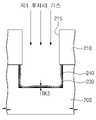
도 1을 참조하면, 상기 플라즈마 식각 장치는, 공정 챔버(100), 피식각막(EL)이 로딩되는 스테이지(110), 플라즈마 발생부(120, 125), 가스 공급부(130) 및 가스 배기부(140)를 포함할 수 있다.Referring to FIG. 1, the plasma etching apparatus includes a
상기 공정 챔버(100)는 플라즈마를 형성하기 위한 식각 가스 또는 플라즈마 상태로 여기된 식각 가스가 유입되는 공간을 포함할 수 있다.The
상기 스테이지(110)는 상기 공정 챔버(100) 내부에 구비되며, 상기 공정 챔버(100) 내부로 제공되는 피식각막(EL)을 지지할 수 있다. 상세하게 도시되지는 않으나, 상기 스테이지(110)는 구동부(도시되지 않음)와 연결되어 상하 구동할 수 있다. 또한, 상기 스테이지(110) 내부에 히터(도시되지 않음)가 구비되어, 상기 식각 공정을 수행하는 동안 상기 피식각막(EL)의 온도를 조절할 수 있다.The
상기 플라즈마 발생부(120, 125)는 상기 공정 챔버(100) 내부로 제공되는 식각 가스를 플라즈마 상태로 여기시키기 위하여 공정 챔버(100)의 상부에 구비되는 상부 전극(120)을 포함할 수 있다.The
상기 상부 전극(120)은 RF 생성부(125)와 연결될 수 있으며, 상기 RF 생성부(125)의 일 단은 접지될 수 있다. 상기 상부 전극(120)에 전압이 인가되면, 상기 상부 전극(120)과 상기 스테이지(110) 사이의 전압 차로 인하여 상기 피식각막(EL) 상에 전계가 형성될 수 있다. 상기 RF 생성부(125)로부터 발생되는 RF 에너지에 의하여 형성된 전계는 상기 식각 가스를 여기시켜 상기 피식각막(EL)을 식각하는 이온과 전자 등으로 분해된 플라즈마 상태를 형성할 수 있다.The
상기 여기된 플라즈마를 상기 피식각막(EL) 상으로 용이하게 유도하기 위하여 상기 피식각막(EL)을 지지하고 있는 하부 전극을 갖는 스테이지(110)에 바이어스 전원부(115)를 연결할 수 있다. 일 예로, 상기 바이어스 전원부(115)에서 RF 에너지를 형성할 수 있다.In order to easily induce the excited plasma onto the film to be etched (EL), a bias
상기 가스 공급부(130)는 상기 공정 챔버(100)의 일 측에 연통되도록 구비될 수 있다. 상기 가스 공급부(130)는 상기 공정 챔버(100) 내부로 식각 가스를 제공할 수 있다. 이때, 상기 공정 챔버(100) 내부로 제공되는 식각 가스는 상기 피식각막(EL)의 종류에 따라 상이할 수 있다. 일 예로, 상기 피식각막(EL)이 실리콘 또는 폴리실리콘을 포함하는 경우, 상기 식각 가스는 SF6, CF4, CF4/H2, CHF3, CF4/O2, HBr, Cl2, 및 Cl2/HBr/O2 중 적어도 하나를 포함할 수 있다. 일 예로, 상기 피식각막(EL)이 실리콘 산화물을 포함하는 경우, 상기 식각 가스는 SF6, NF3, CF4, CF4/H2, CHF3/O2, CF4/O2, C2H6, C3H8, 및 CHF3/C4F8/CO 중 적어도 하나를 포함할 수 있다. 일 예로, 상기 피식각막(EL)이 실리콘 질화물을 포함하는 경우, 상기 식각 가스는 CF4/O2, CF4/H2, CHF3/O2, 및 CH2F2 중 적어도 하나를 포함할 수 있다. 일 예로, 상기 피식각막(EL)이 알루미늄을 포함하는 경우, 상기 식각 가스는 Cl2, Cl2/CHCl3, 및 Cl2/N2 중 적어도 하나를 포함할 수 있다. 일 예로, 상기 피식각막(EL)이 텅스텐을 포함하는 경우, 상기 식각 가스는 SF6, CF4, 및 Cl2 중 적어도 하나를 포함할 수 있다. 상기 피식각막(EL)이 티타늄 또는 티타늄 질화물을 포함하는 경우, 상기 식각 가스는 Cl2, Cl2/CHCl3, 및 CF4 중 적어도 하나를 포함할 수 있다. 상기 피식각막(EL)이 티타늄 실리사이드를 포함하는 경우, 상기 식각 가스는 Cl2, Cl2/CHCl3, 및 CF4/O2중 적어도 하나를 포함할 수 있다.The
상기 가스 배기부(140)는 상기 공정 챔버(100)의 일 측에 연통되도록 구비되며, 진공 밸브(도시되지 않음) 및 진공 펌프(도시되지 않음)를 포함할 수 있다. 구체적으로, 상기 가스 배기부(140)는 상기 공정 챔버(100) 내부의 압력을 조절하는 역할 및 식각 공정 시 발생되는 식각 부산물들을 배출하는 역할을 할 수 있다. 상기 공정 챔버(100) 내부의 압력 조절 및 상기 식각 부산물을 배출하기 위해 상기 진공 밸브가 개방되면서 상기 진공 펌프가 작동될 수 있다.The
도 1에 도시된 플라즈마 식각 장치는 예시적인 것으로 본 발명에서 상기 플라즈마 식각 장치를 이것으로 한정하는 것은 아니다.The plasma etching device shown in FIG. 1 is illustrative, and the plasma etching device is not limited thereto in the present invention.
도 2는 본 발명의 실시예들에 따른 식각 후처리 방법을 설명하기 위한 순서도이다. 도 3 내지 도 9는 본 발명의 실시예들에 따른 반도체 소자를 형성하기 위한 방법을 설명하기 위한 단면도들이다.2 is a flowchart illustrating a post-etching processing method according to embodiments of the present invention. 3 to 9 are cross-sectional views illustrating a method of forming a semiconductor device according to example embodiments.
도 3을 참조하면, 피식각막(200) 상에 마스크 패턴(210)을 형성할 수 있다.Referring to FIG. 3 , a
상기 마스크 패턴(210)은 상기 피식각막(200)의 일부를 노출시키는 개구(215)를 포함할 수 있다. 예컨대, 상기 개구(215)는 홀 형상이거나 일 방향으로 연장하는 라인 형상을 가질 수 있다. 그러나, 본 발명에서 상기 개구(215)의 형상을 이로 한정하는 것은 아니다.The
상기 피식각막(200)은 기판, 절연막 및/또는 도전막을 포함할 수 있다. 일 예로, 상기 피식각막(200)이 기판일 경우, 상기 기판은 실리콘 및/또는 게르마늄을 포함하는 반도체 기판이거나, SOI(silicon on insulation) 기판 또는 GOI(germanium on insulation) 기판을 포함할 수 있다. 일 예로, 상기 피식각막(200)이 절연막일 경우, 상기 절연막은 실리콘 산화물, 실리콘 질화물 또는 실리콘 산질화물 중 하나를 포함할 수 있다. 일 예로, 상기 피식각막(200)이 도전막일 경우, 상기 도전막은 폴리실리콘, 알루미늄, 텅스텐, 티타늄, 티타늄 질화물 및 티타늄 실리사이드 중 하나를 포함할 수 있다.The film to be etched 200 may include a substrate, an insulating film, and/or a conductive film. For example, when the film to be etched 200 is a substrate, the substrate may include a semiconductor substrate including silicon and/or germanium, a silicon on insulation (SOI) substrate, or a germanium on insulation (GOI) substrate. For example, when the film to be etched 200 is an insulating film, the insulating film may include one of silicon oxide, silicon nitride, and silicon oxynitride. For example, when the layer to be etched 200 is a conductive layer, the conductive layer may include one of polysilicon, aluminum, tungsten, titanium, titanium nitride, and titanium silicide.
상기 마스크 패턴(210)은 상기 피식각막(200)에 대하여 식각 선택비를 갖는 물질을 포함할 수 있다. 예컨대, 상기 마스크 패턴(210)은 포토레지스트 물질 또는 실리콘 질화물과 같은 절연물을 포함할 수 있다.The
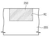
도 2 및 도 4를 참조하면, 상기 마스크 패턴(210)을 식각 마스크로 사용하여 상기 피식각막(200)을 식각하여 패턴 구조물(205)을 형성할 수 있다.(단계 S100) 상기 패턴 구조물(205)은 리세스(RC)를 포함할 수 있다.Referring to FIGS. 2 and 4 , the
실시예들에 따르면, 상기 피식각막(200)을 식각하는 것은 플라즈마를 이용한 이방성 식각일 수 있다. 상기 이방성 식각은 도 1에 도시된 플라즈마 식각 장치를 이용하여 수행될 수 있다.According to embodiments, etching the film to be etched 200 may be anisotropic etching using plasma. The anisotropic etching may be performed using the plasma etching apparatus shown in FIG. 1 .
상기 플라즈마 상태의 반응 가스가 상기 마스크 패턴(210)에 의해 노출된 피식각막(200)을 이방성으로 식각하면, 완성된 패턴 구조물(205)의 리세스(RC) 표면에는 플라즈마 손상을 입게 된다. 상기 플라즈마에 의해 손상되는 정도가 영역마다 상이할 수 있다. 도 2에 도시된 바와 같이, 상기 리세스(RC) 바닥면이 측면보다 더 많이 받으며, 상기 바닥면 및 측면이 만나는 모서리 부분에서 가장 많이 받을 수 있다. 설명의 용이함을 위하여 이하에서 손상된 영역의 두께를 가장 많이 손상 받은 부분의 두께로 일괄적으로 설명하기로 한다. 또한, 상기 식각 공정으로 손상된 부분의 손상 두께를 제1 두께(TK1)라 하며, 상기 손상된 영역을 제1 손상 영역(220)이라 한다. 상기 제1 손상 영역(220)은 내부의 원자들 사이의 결합이 약화되거나 끊어져 결합이 불안정하며, 외부의 충격에 의해 상기 패턴 구조물(205)로부터 쉽게 제거될 수 있다.When the reactive gas in the plasma state anisotropically etches the film to be etched 200 exposed by the
한편, 상기 식각 공정 후, 식각 잔류물(RSD)이 상기 패턴 구조물(205)의 리세스 표면에 잔류할 수 있다.Meanwhile, after the etching process, etching residue RSD may remain on the recessed surface of the
도 2 및 도 5를 참조하면, 상기 식각 공정을 수행한 챔버(100, 도 1 참조)와 동일한 챔버에서 인-시튜(in-situ)로 일차 식각 후처리(first post etch treatment) 공정을 수행할 수 있다. (단계 S120) 다른 실시예에 따르면, 상기 일차 식각 후처리 공정은 상기 식각 공정을 수행한 챔버에서 진행되지 않을 수도 있다.2 and 5, a first post etch treatment process is performed in-situ in the same chamber as the chamber (100, see FIG. 1) in which the etching process was performed. can (Step S120) According to another embodiment, the first post-etching process may not be performed in the chamber in which the etching process is performed.
상기 일차 식각 후처리 공정은 상기 제1 손상 영역(220)을 제거하기 위한 공정이다. 본 발명의 일 실시예에 따르면, 상기 일차 식각 후처리 공정은 도 1에 도시된 공정 챔버(100, 도 1 참조)로 제1 후처리 가스를 주입한 후, 플라즈마를 발생시켜 수행될 수 있다. 플라즈마 상태의 제1 후처리 가스의 이온들은 식각 공정으로 손상된 제1 손상 영역(220)이 형성된 패턴 구조물(205)의 표면에 스퍼터될 수 있다. 스퍼터된 이온들은 제1 손상 영역(220)에 충돌함으로써 상기 제1 손상 영역(220) 및 식각 잔류물(RSD)을 상기 패턴 구조물(205)로부터 제거할 수 있다.The post-primary etching process is a process for removing the first
상기 식각 잔류물(RSD)은 상기 제1 후처리 가스에 의해 먼저 제거될 수 있다. 이어서, 상기 제1 손상 영역(220)을 제거할 수 있다. 상기 제1 손상 영역(220)을 제거하는 공정을 아래에서 상세하게 설명한다.The etching residue RSD may be first removed by the first post-processing gas. Subsequently, the first
본 발명의 일 실시예에 따르면, 상기 제1 후처리 가스의 종류 또는 유량 등을 조절하여, 상기 제1 후처리 가스의 플라즈마 이온들의 충돌 깊이(즉, 제2 깊이)를 조절할 수 있다. 상기 제1 후처리 가스의 이온들의 충돌 깊이는 상기 제1 두께(TK1)와 실질적으로 동일한 것이 바람직하다.According to an embodiment of the present invention, a collision depth (ie, a second depth) of plasma ions of the first post-processing gas may be adjusted by adjusting the type or flow rate of the first post-processing gas. A collision depth of the ions of the first post-processing gas may be substantially the same as the first thickness TK1 .
일 실시예에 따르면, 상기 제1 손상 영역(220)만을 제거하는 것이 바람직하나, 전술한 바와 같이 상기 식각 공정에 의해 손상되는 부위가 상기 패턴 구조물(205)의 위치에 따라 그 깊이가 상이하여, 상기 식각 공정에서 손상되지 않은 부위까지 상기 제1 후처리 가스의 이온들에 의해 손상될 수 있다. 또한, 상기 일차 식각 후처리 공정을 진행하는 중 공정 변수들이 발생할 수 있으며, 공정 변수들을 고려하여 상기 제1 손상 영역(220)뿐만 아니라 손상되지 않은 패턴 구조물의 일부까지 상기 일차 후처리 공정이 수행될 수 있다. 따라서, 상기 일차 식각 후처리 공정에 의해 패턴 구조물(205)의 리세스의 표면의 일부가 손상될 수 있으며, 이하 설명의 용이함을 위하여, 상기 제1 후처리 가스의 이온들에 의해 손상된 부위를 제2 손상 영역(230)이라 한다. 또한, 상기 제2 손상 영역(230)의 두께는 상기 패턴 구조물(205)의 리세스 측면 및 바닥면 등의 위치에 따라 상이하나, 전술한 바와 같이 가장 두껍게 손상된 부분의 두께를 상기 제2 손상 영역(230)의 두께라 하며 설명의 용이함을 위해 제2 두께(TK2)라 한다. 상기 제2 두께(TK2)는 상기 제1 손상 영역(220)이 제거된 리세스의 표면으로부터 상기 제2 손상 영역(230)의 바닥면까지의 거리일 수 있다.According to one embodiment, it is preferable to remove only the first damaged
다른 실시예에 따르면, 상기 일차 후처리 공정은 상기 제1 손상 영역(220)만을 제거할 수 있다. 이 경우, 상기 제2 손상 영역(230)은 생성되지 않을 수 있다. 다만, 상기 일차 후처리 공정에 의해 식각 잔류물(RSD)이 잔류하여 후속되는 이차 식각 후처리 공정을 수행할 수 있다.According to another embodiment, the primary post-processing process may remove only the first
일 실시예에서, 상기 제1 후처리 가스의 이온들의 전하와 바이어스 전원이 인가된 스테이지(110, 도 1 참조)의 전하를 이용하여 상기 이온들의 충돌 깊이를 조절할 수 있다. 구체적으로 설명하면, 상기 제1 후처리 가스에서 플라즈마에 의해 상태 변화한 이온들의 전하는, 상기 바이어스 전원(115, 도 1 참조)에 의해 인가된 스테이지(110)의 전하와 동일할 수 있다. 상기 이온의 전하와 상기 스테이지(110)에 인가된 전하가 동일함으로써, 둘 사이 반발력이 발생하고 이를 이용하여 상기 패턴 구조물(205)의 리세스 표면으로 투과하는 이온들의 양 또는 이온들이 투과되는 깊이가 감소할 수 있다. 따라서, 상기 패턴 구조물(205)이 상기 제1 후처리 가스의 이온들에 의해 손상되는 제2 손상 영역(230)의 두께(TK2)를 감소시킬 수 있다. 일 실시예에 따르면, 상기 제1 후처리 가스는 탄소를 포함하지 않은(carbon free) 가스를 포함할 수 있다. 상기 제1 후처리 가스는 플루오르(F), 염소(Cl) 및 브롬(Br)과 같은 할로겐족 중 적어도 하나를 포함할 수 있다. 예컨대, 상기 제1 후처리 가스는 SF6, HBr, NF3, 및 Cl2 중 적어도 하나를 포함할 수 있다.In one embodiment, the collision depth of the ions may be adjusted using the charge of the ions of the first post-processing gas and the charge of the stage 110 (see FIG. 1) to which bias power is applied. Specifically, the charge of the ions whose state has been changed by plasma in the first post-processing gas may be the same as the charge of the
다른 실시예에서, 상기 제1 후처리 가스의 특성을 이용하여, 상기 제1 후처리 가스의 이온들의 충돌 깊이를 조절할 수 있다. 구체적으로 설명하면, 상기 제1 후처리 가스에서 플라즈마에 의해 상태 변화한 이온들 자체가 충돌력이 크지 않은 제1 후처리 가스를 선택할 수 있다. 이로써, 상기 이온들이 상기 패턴 구조물(205)의 리세스(RC) 표면으로 충돌하더라도, 깊게 충돌하지 못할 수 있다. 이러한 특성으로 상기 제1 후처리 가스의 이온들이 상기 제1 두께를 지나치게 넘어가지 않아, 상기 패턴 구조물(205) 표면이 손상되는 것을 방지할 수 있다.In another embodiment, a collision depth of ions of the first post-processing gas may be adjusted using characteristics of the first post-processing gas. Specifically, the first post-processing gas may be selected so that the collision force of the ions changed by the plasma in the first post-processing gas is not large. Thus, even if the ions collide with the surface of the recess RC of the
도 5에서는 상기 제1 손상 영역(220)이 완전하게 제거된 것으로 도시되었으나, 상기 제1 손상 영역(220)의 일부가 잔류할 수도 있다. 또한, 상기 제1 손상 영역(220) 아래에 상기 식각 공정으로 손상되지 않은 패턴 구조물(205)의 표면의 일부가 제거될 수 있다.Although the first
또한, 상기 일차 식각 후처리 공정에서, 상기 패턴 구조물(205)의 리세스 표면에 상기 패턴 구조물(205) 표면에 상기 일차 후처리 공정에 사용되는 이온들(예를 들면, C+, Cl-, F-)이 오염 물질(RSD)로 잔류하게 될 수도 있다. 상기 오염 물질들(RSD)은 상기 제2 손상 영역(230)이 형성된 패턴 구조물(205) 표면에 잔류할 수 있다. 상기 오염 물질들(RSD)은 후속 완성되는 반도체 소자에서 결함으로 작용하여, 상기 반도체 소자의 전기적 신뢰성을 저하시킬 수 있다.In addition, in the first post-etching process, ions (eg, C+ , Cl - , C + , Cl- , F- ) may remain as a contaminant (RSD). The contaminants RSD may remain on the surface of the
도 2 및 도 6을 참조하면, 상기 일차 식각 후처리 공정을 수행한 챔버와 동일한 챔버에서 인-시튜로 이차 식각 후처리 공정을 수행할 수 있다. (단계 S130) 다른 실시예에 따르면, 상기 이차 후처리 공정은 상기 일차 후처리 공정이 수행된 챔버와 다른 챔버에서 수행될 수도 있다.Referring to FIGS. 2 and 6 , a second post-etch process may be performed in-situ in the same chamber as the chamber in which the first post-etch process is performed. (Step S130) According to another embodiment, the secondary post-processing process may be performed in a chamber different from the chamber in which the primary post-processing process is performed.
도 2 및 도 5에서 설명된 바와 같이 상기 일차 식각 후처리 공정 후 상기 패턴 구조물(205)의 표면에 제2 손상 영역(230)이 형성되고 오염 물질(RSD)이 잔류할 수 있다. 상기 이차 식각 후처리 공정은 반응성이 없는 제2 후처리 가스를 이용하여 상기 제2 손상 영역(230)에 손상을 입히고, 상기 오염 물질(RSD)을 제거할 수 있다.As described with reference to FIGS. 2 and 5 , second
본 발명의 일 실시예에 따르면, 상기 이차 식각 후처리 공정은 도 1에 도시된 공정 챔버(100, 도 1 참조)로 제2 후처리 가스를 주입한 후, 플라즈마를 발생시켜 수행될 수 있다. 본 발명의 실시예들에 따르면, 상기 제2 후처리 가스는 불활성 가스를 포함할 수 있다. 예컨대, 상기 제2 후처리 가스는 헬륨(He), 아르곤(Ar) 및 질소(N2)으로 이루어진 군으로부터 선택된 적어도 하나를 포함할 수 있다.According to an embodiment of the present invention, the secondary etching post-processing process may be performed by injecting a second post-processing gas into the process chamber 100 (see FIG. 1) shown in FIG. 1 and then generating plasma. According to embodiments of the present invention, the second post-processing gas may include an inert gas. For example, the second post-processing gas may include at least one selected from the group consisting of helium (He), argon (Ar), and nitrogen (N2 ).
상기 이차 식각 후처리 공정에서, 상기 패턴 구조물(205)의 표면에 잔류하는 오염 물질들(RSD)을 물리적으로 탈착시켜 제거할 수 있다. 또한, 상기 불활성 가스를 이용하는 플라즈마 공정을 통해, 상기 제2 손상 영역(230)에 물리적인 손상만을 입히며, 더 이상의 오염물질을 생성시키지 않을 수 있다. 상기 제2 손상 영역(230)은 상기 이차 식각 후처리 공정에 의해 물리적으로 손상을 입어 그 내부의 결합이 약화되거나 끊어질 수 있다.In the post-secondary etching process, contaminants RSD remaining on the surface of the
일 실시예에 따르면, 상기 이차 식각 후처리 공정에서, 상기 제2 손상 영역(230)만 손상시키는 것이 바람직하다. 그러나, 상기 제2 손상 영역(230)의 두께(TK2)가 상기 패턴 구조물(205)의 위치에 따라 동일하지 않을 수 있고, 상기 이차 후처리 공정을 진행하는 중 공정 변수들이 발생할 수 있다. 따라서, 상기의 제2 손상 영역(230)의 불균일한 두께(TK2)와 공정 변수들을 고려하여 상기 제2 손상 영역(230)뿐만 아니라 손상되지 않은 패턴 구조물(205)의 일부까지 상기 이차 후처리 공정이 수행될 수 있다.According to an embodiment, it is preferable to damage only the second
상기 이차 식각 후처리 공정에 의해 손상된 부분을 제3 손상 영역(240)이라 하며, 상기 제3 손상 영역(240)은 상기 제2 손상 영역(230) 감싸며 형성될 수 있다. 또한, 상기 제3 손상 영역(240)의 두께는 상기 패턴 구조물의 리세스 측면 및 바닥면 등의 위치에 따라 상이하나, 전술한 바와 같이 가장 두껍게 손상된 부분의 두께를 상기 제3 손상 영역(240)의 두께라 하며 설명의 용이함을 위해 제3 두께(TK3)라 한다. 상기 제3 두께(TK3)는 상기 제1 손상 영역(220)이 제거된 리세스의 표면으로부터 상기 제3 손상 영역(240)의 바닥면까지의 거리일 수 있다. 상기 제3 두께(TK3)는 상기 제2 두께(TK2)보다 클 수 있다.A portion damaged by the secondary etching post-processing process is referred to as a third
다른 실시예에 따르면, 상기 이차 식각 후처리 공정은 상기 제2 손상 영역(230)만을 손상시킬 수 있다. 이 경우, 상기 제3 손상 영역(240)은 생성되지 않을 수 있다.According to another embodiment, the second post-etching process may damage only the second
도 2 및 도 7을 참조하면, 상기 제2 및 제3 손상 영역들(230, 240)을 제거하기 위한 세정 공정을 수행할 수 있다. (단계 S140)Referring to FIGS. 2 and 7 , a cleaning process may be performed to remove the second and third
본 발명의 실시예들에 따르면, 상기 제2 및 제3 손상 영역들(230, 240)은 제거 공정은 애싱 공정 없이, 스트립 공정만으로 수행될 수 있다.According to embodiments of the present invention, the removal process of the second and third
일반적으로, 플라즈마 공정의 부산물을 애싱 공정과 스트립 공정으로 제거되는데, 본 발명의 실시예들에 따르면, 상기 제2 및 제3 손상 영역들(230, 240) 각각이 상기 제1 후처리 가스의 이온들 및 상기 제2 후처리 가스 이온들에 의해 손상된 부분들로서, 그 내부의 결합이 약하거나 끊어져서 상기 스트립 공정 만으로도 상기 패턴 구조물(205)로부터 용이하게 제거될 수 있다.In general, by-products of the plasma process are removed by an ashing process and a strip process. According to embodiments of the present invention, the second and third
본 발명의 실시예들에 따르면, 상기 제거 공정은 습식 세정 공정 및 건식 세정 공정 중 적어도 하나를 포함할 수 있다. 상기에서 설명한 것과 유사하게, 제2 및 제3 손상 영역들(230, 240) 각각은 상기 제1 후처리 가스의 이온들 및 상기 제2 후처리 가스 이온들에 의해 손상된 부분들로서, 그 내부의 결합이 약하거나 끊어져서 습식 또는 건식 세정 공정으로 용이하게 제거될 수 있다.According to embodiments of the present invention, the removal process may include at least one of a wet cleaning process and a dry cleaning process. Similar to what has been described above, each of the second and third
상기 패턴 구조물(205)의 리세스(RC) 내부에 다양한 물질을 채워 다양한 반도체 소자로 사용할 수 있다.Various materials may be filled in the recesses RC of the
도 8에 도시된 일 실시예에 따르면, 상기 패턴 구조물(205)의 리세스(RC) 내부를 도전물로 채워 콘택 플러그(250, 또는 배선)를 포함하는 반도체 소자를 완성할 수 있다. 상기 콘택 플러그(250, 또는 배선)와 상기 패턴 구조물(205) 사이에 손상된 영역이 있는 경우, 그 영역에서 누설 전류가 발생할 수 있으나, 본 실시예들에 따라 상기 손상 영역들을 제거함으로써 전기적 특성 열화를 방지할 수 있다.According to the embodiment shown in FIG. 8 , a semiconductor device including a contact plug 250 (or wiring) may be completed by filling the inside of the recess RC of the
도 9에 도시된 일 실시예에 따르면, 상기 패턴 구조물(205) 상에 에피택시얼(epitaxial) 공정을 이용하여, 에피 패턴(260)을 포함하는 반도체 소자를 완성할 수 있다. 상세하게 도시되지 않았으나, 상기 패턴 구조물(205)의 리세스(RC) 내측면을 따라 시드막(seed layer)을 형성할 수 있다. 상기 에피 패턴(260)과 상기 패턴 구조물(205) 사이에 손상된 영역이 있는 경우, 그 영역에서 누설 전류가 발생할 수 있으나, 본 실시예들에 따라 상기 손상 영역들을 제거함으로써 전기적 특성 열화를 방지할 수 있다.According to the exemplary embodiment shown in FIG. 9 , a semiconductor device including an
본 발명에서는 상기 리세스(RC) 내부를 채우는 공정은 도 6 및 도 7을 참조하여 예시적으로 설명하였으나, 본 발명이 이로 한정되는 것은 아니다.In the present invention, the process of filling the inside of the recess RC has been exemplarily described with reference to FIGS. 6 and 7 , but the present invention is not limited thereto.
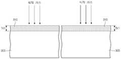
도 10 내지 도 13은 비교예에 따른 식각 후처리 방법 및 본 발명의 실시예에 따른 식각 후처리 방법을 설명하기 위한 단면도들이다. 도 10 내지 도 13의 왼쪽이 비교예를 도시하며, 오른쪽이 본 발명의 실시예를 도시한다.도 10을 참조하면, 본 발명의 실시예에 따른 피식각막(300) 및 일반적인 피식각막(305) 모두를 CF4가스를 이용하여 플라즈마 식각하면, 제1 손상 두께(TK1)로 제1 손상 영역들(310, 315)이 각각 형성된다. 상기 제1 손상 영역들(310, 315) 각각은 그 내부의 결합이 약하거나 끊어진 상태일 수 있다.10 to 13 are cross-sectional views illustrating a post-etching treatment method according to a comparative example and a post-etching treatment method according to an embodiment of the present invention. 10 to 13, the left side shows a comparative example, and the right side shows an embodiment of the present invention. Referring to FIG. 10, a cornea to be etched 300 according to an embodiment of the present invention and a
도 11의 왼쪽을 참조하면, 비교예에 따라 상기 피식각막(300) 표면에 일반적인 일차 식각 후처리 공정을 수행한다. 상기 일차 식각 후처리 공정은 식각 공정 시 사용되는 식각 가스와 동일한 가스를 사용한다. 구체적으로 설명하면, CF4가스를 이용하며, 상기 피식각막이 로딩된 스테이지로 음의 바이어스(bias)가 인가된다. CF4가스는 C+, F-, CF3, F 등으로 분해된다. 상기 분해된 원소들이 상기 제1 손상 영역(310)이 형성된 피식각막(300) 표면에 충돌하여, 상기 제1 손상 영역(310)을 제거한다. 그런데, 상기 분해된 원소들이 제1 손상 영역(310)뿐만 아니라 그 아래의 피식각막(305)까지 침투하게 되어 제2 손상 영역(320)을 형성하게 된다. 특히, C+는 원자량이 작고, 음의 바이어스를 갖는 스테이지와의 인력으로 상기 피식각막(300) 내측으로 깊게 침투하게 되며, 이는 오염층으로써 후속 완성되는 소자의 전기적 신뢰성을 저하시킨다. 상기 제2 손상 영역(320)은 제2 손상 두께(TK2)를 갖는데, 상기 제2 손상 두께(TK2)는 상기 제1 손상 영역(310)이 제거된 피식각막(300) 표면으로부터 상기 제2 손상 영역(320)의 바닥면까지의 거리이다.Referring to the left side of FIG. 11 , a general post-etching process is performed on the surface of the film to be etched 300 according to a comparative example. The first post-etching process uses the same gas as the etching gas used in the etching process. Specifically, CF4 gas is used, and a negative bias is applied to the stage loaded with the film to be etched. CF4 gas is decomposed into C+ , F- , CF3 , F and the like. The decomposed elements collide with the surface of the etched
도 11의 오른쪽을 참조하면, 본 실시예에 따라 상기 피식각막(305) 표면에 일차 식각 후처리 공정을 수행한다. 상기 일차 후처리 공정은 본 실시예에서는 상기 일차 식각 후처리 공정을 Cl2가스를 이용한 플라즈마 공정을 사용한다. 또한, 상기 피식각막(305)이 로딩된 스테이지로 음의 바이어스가 인가된다. 상기 Cl2 가스가 플라즈마 상태의 라디칼(Cl*) 또는 음의 이온들(Cl-)로 분해된다. 상기 분해된 원소들이 상기 제1 손상 영역(315)이 형성된 피식각막(305) 표면에 충돌하여, 상기 제1 손상 영역(315)을 제거한다. 그런데, 상기 분해된 원소들이 제1 손상 영역(315)뿐만 아니라 그 아래의 기판까지 침투하게 되어 제3 손상 영역(325)을 형성하게 된다. 본 실시예에 따르면, 음의 바이어스를 갖는 스테이지와 상기 Cl-는 반발력에 의해 상기 제3 손상 영역(325)은 상기 제2 두께(TK2)보다 작은 제3 두께(TK3)를 갖는다.Referring to the right side of FIG. 11 , a first post-etching process is performed on the surface of the film to be etched 305 according to the present embodiment. In the first post-processing process, in this embodiment, a plasma process using Cl2 gas is used for the first post-etching process. In addition, a negative bias is applied to the stage on which the etched
도 12의 왼쪽을 참조하면, 상기 제2 손상 영역(320)으로 이차 후처리 공정을 수행한다. 본 공정은 통상의 식각 후처리 공정에서 없는 공정이다. 그러나, 본 발명의 일차 후처리 공정에 관련된 특징을 변수로 하기 위하여, 본 이차 후처리 공정을 비교예에서 동일하게 수행한다.Referring to the left side of FIG. 12 , a secondary post-processing process is performed on the second damaged
구체적으로 Ar가스와 같은 불활성 가스를 이용하는 플라즈마 공정을 수행하여, 상기 제2 손상 영역(320)으로 물리적 충격을 가하여 물리적 손상을 입힌다. 이때, 상기 이차 후처리 공정에 의해 손상되는 두께는 상기 제2 두께(TK2)보다 작은 제4 두께(TK4)를 갖는다. 이는, 상기 일차 식각 후처리 공정 시, 사용된 CF4 가스 내 C+는 원자량이 작고, 음의 바이어스를 갖는 스테이지와의 인력으로 상기 기판 내측으로 깊게 침투함으로써, 일차 식긱 후처리 공정 후 손상 받은 부위가 깊게 형성되었고, 상기 이차 식각 후처리 공정 시, 불활성 가스는 상기 일차 식각 후처리 공정 시 손상 받은 깊이보다 작게 침투되기 때문이다.Specifically, by performing a plasma process using an inert gas such as Ar gas, a physical impact is applied to the second damaged
상기 이차 후처리 공정에 의해 손상 받은 부분을 제4 손상 영역(330)이라하며, 상기 제4 손상 영역(330)은 상기 제2 손상 영역(320)의 상부에 포함된다. 또한, 상기 제4 손상 영역(330)은 상기 피식각막(305) 상부면에서 상기 제4 손상 영역(330)의 바닥면까지의 제4 두께(TK4)를 갖는다. 상기 제4 두께(TK4)는 상기 제2 두께(TK2)보다 작다.A portion damaged by the secondary post-processing process is referred to as a fourth
상기 이차 후처리 공정으로 상기 제2 손상 영역(320)의 상부 일부 즉, 제4 손상 영역(330)에만 손상을 입히게 된다. 손상을 입은 제2 손상 영역(320)의 상부(제4 손상 영역, 330)는 그 결합이 약해지거나 끊어진 상태로 후속 세정 공정에서 용이하게 제거될 수 있으나, 손상 입지 않은 제2 손상 영역의 하부(320L)는 상부보다 제거되기 어렵다.In the secondary post-processing process, only the upper portion of the second
도 12의 오른쪽을 참조하면, 상기 제3 손상 영역(325)으로 이차 후처리 공정을 수행한다. 구체적으로 도 12a에서 수행된 이차 후처리 공정과 실질적으로 동일하며, 즉, 플라즈마 Ar가스와 같은 불활성 가스를 이용하는 플라즈마 공정을 수행하여, 상기 제3 손상 영역(325D)으로 물리적 충격을 가하여 물리적 손상을 입힌다. 더불어, 상기 제3 손상 영역(325D) 아래에 상기 이차 후처리 공정에 의해 손상되는 제5 손상 영역(335)이 형성될 수 있다. 상기 이차 후처리 공정으로 손상된 부위는 피식각막(305)의 상부면으로부터 상기 제5 손상 영역(335)의 바닥면까지 제5 두께(TK5)를 가질 수 있다. 상기 제5 두께(TK5)는 상기 제3 두께(TK3)보다 크며, 상기 제4 두께(TK4)와 실질적으로 동일하다.Referring to the right side of FIG. 12 , a secondary post-processing process is performed on the third
상기 이차 후처리 공정으로, 상기 제3 손상 영역(325D)은 물리적으로 더 손상을 받게 되고, 상기 제5 손상 영역(335)은 불활성 가스를 사용함으로써 손상된 부위의 오염이 발생하지 않는다.In the secondary post-processing process, the third
도 13의 왼쪽을 참조하면, 세정 공정을 수행한다. 상기 세정 공정은 애싱 공정 및 스트립 공정을 포함하는 두 단계로 진행하되, 상기 제4 손상 영역(제2 손상 영역의 상부, 330)은 제거되지만 상기 이차 식각 후처리 공정에서 손상 받지 못한 제2 손상 영역 하부(320R)는, 그 내부에 잔류하는 C+, F-, CF3, F 등에 의해 완전하게 제거되지 못한다. 제거되지 않은 제2 손상 영역(320R)은 완성되는 소자의 전기적 신뢰성을 저하시킬 수 있다.Referring to the left side of FIG. 13 , a cleaning process is performed. The cleaning process proceeds in two stages including an ashing process and a stripping process, wherein the fourth damaged area (upper part of the second damaged area 330) is removed, but the second damaged area not damaged in the secondary etching post-processing process. The
도 13의 오른쪽 참조하면, 세정 공정을 수행하되, 상기 세정 공정은 애싱 공정 없이 스트립 공정으로 진행된다. 상기 세정 공정에 의해 물리적 손상을 받은 상기 제3 손상 영역(325D) 및 상기 제5 손상 영역(335)이 제거된다.Referring to the right side of FIG. 13 , a cleaning process is performed, but the cleaning process proceeds as a strip process without an ashing process. The third
도 14는 본 발명의 실시예들에 따른 반도체 소자의 형성 방법으로 형성된 패턴 구조물 표면의 탄소 양과, 비교예에 따른 반도체 소자의 형성 방법으로 형성된 패턴 구조물 표면의 탄소 양을 비교한 그래프이다.14 is a graph comparing the amount of carbon on the surface of a pattern structure formed by the method of forming a semiconductor device according to embodiments of the present invention and the amount of carbon on the surface of a pattern structure formed by the method of forming a semiconductor device according to a comparative example.
도 14를 참조하면, 본 발명의 실시예들에 따라 형성된 패턴 구조물의 표면의 탄소 양이 비교예에 따라 형성된 패턴 구조물의 표면의 탄소 양보다 실질적으로 절반 이상 적은 것을 알 수 있다. 이는, 본 발명의 실시예들에 따라 일차 식각 후처리 공정 시, 탄소를 포함하지 않으며 스테이지의 전하와 동일한 전하의 후처리 식각 가스를 사용하거나, 패턴 구조물 표면으로 투과되기 어려운 가스를 사용함으로써 탄소의 양을 감소시킨다.Referring to FIG. 14 , it can be seen that the amount of carbon on the surface of the pattern structure formed according to the embodiments of the present invention is substantially less than half of the amount of carbon on the surface of the pattern structure formed according to the comparative example. This is achieved by using a post-processing etching gas that does not contain carbon and has the same charge as the charge of the stage in the first post-etching process according to embodiments of the present invention, or by using a gas that is difficult to penetrate into the surface of the pattern structure. reduce the amount
이상, 첨부된 도면을 참조하여 본 발명의 실시예를 설명하였지만, 본 발명이 속하는 기술분야에서 통상의 지식을 가진 자는 본 발명이 그 기술적 사상이나 필수적인 특징으로 변경하지 않고서 다른 구체적인 형태로 실시될 수 있다는 것을 이해할 수 있을 것이다. 그러므로 이상에서 기술한 실시예에는 모든 면에서 예시적인 것이며 한정적이 아닌 것으로 이해해야만 한다.Although the embodiments of the present invention have been described with reference to the accompanying drawings, those skilled in the art can implement the present invention in other specific forms without changing its technical spirit or essential features. You will understand that there is Therefore, it should be understood that the embodiments described above are illustrative in all respects and not restrictive.
200: 피식각막
205: 패턴 구조물
210: 마스크 패턴
220: 제1 손상 영역
230: 제2 손상 영역
240: 제3 손상 영역200: cornea to be etched
205: pattern structure
210: mask pattern
220 First damaged area
230: second damaged area
240 Third damaged area
Claims (10)
Translated fromKorean상기 플라즈마 장치로 식각 가스를 주입하고 상기 피식각막을 플라즈마 식각하는 단계;
상기 피식각막을 플라즈마 식각하는 동안, 상기 식각된 피식각막 표면에 제1 두께로 손상된 제1 영역이 생성되는 단계;
상기 플라즈마 식각된 피식각막의 표면으로 제1 후처리 가스를 주입하는 일차 플라즈마 후처리 공정을 수행하여, 상기 제1 영역을 제거하는 단계;
상기 일차 플라즈마 후처리 공정 동안, 상기 제1 영역이 제거된 피식각막 표면에 제2 두께로 손상된 제2 영역이 생성되는 단계;
상기 제2 영역이 생성된 피식각막 표면으로 제2 후처리 가스를 주입하는 이차 플라즈마 후처리 공정을 수행하여, 상기 제2 영역을 재손상시키는 단계; 및
상기 재손상된 제2 영역을 세정 공정으로 제거하는 단계를 포함하는 식각 후처리 방법.loading a film to be etched onto a stage in a plasma apparatus;
injecting an etching gas into the plasma device and plasma etching the film to be etched;
generating a damaged first region having a first thickness on a surface of the etched film to be etched while plasma etching the film to be etched;
removing the first region by performing a first plasma post-treatment process of injecting a first post-treatment gas into the surface of the plasma-etched film to be etched;
generating a damaged second region having a second thickness on the surface of the etchant film from which the first region was removed during the primary plasma post-treatment process;
re-damaging the second region by performing a secondary plasma post-treatment process of injecting a second post-treatment gas into the surface of the film to be etched where the second region is formed; and
and removing the re-damaged second region through a cleaning process.
상기 제1 후처리 가스로 일차 플라즈마 후처리하는 동안, 플라즈마 상태의 제1 후처리 가스의 이온들의 전하(charge)가 상기 스테이지에 인가되는 바이어스 전원의 전하와 동일한 식각 후처리 방법.According to claim 1,
During primary plasma post-processing with the first post-processing gas, the charge of ions of the first post-processing gas in a plasma state is the same as the charge of the bias power applied to the stage.
상기 플라즈마 식각하는 단계, 상기 일차 플라즈마 후처리 공정을 수행하여, 상기 제1 영역을 제거하는 단계 및 이차 플라즈마 후처리 공정을 수행하여, 상기 제2 영역을 재손상시키는 단계는 동일한 상기 플라즈마 장치 내에서(in-situ) 수행되는 식각 후처리 방법.According to claim 1,
The plasma etching, removing the first region by performing the first plasma post-treatment process, and re-damaging the second region by performing a secondary plasma post-treatment process are performed in the same plasma device. Post-etch processing method performed in-situ.
상기 플라즈마 식각하는 단계, 상기 일차 플라즈마 후처리 공정을 수행하여, 상기 제1 영역을 제거하는 단계 및 이차 플라즈마 후처리 공정을 수행하여, 상기 제2 영역을 재손상시키는 단계 중 적어도 두 단계가 동일한 상기 플라즈마 장치에서 수행되는 식각 후처리 방법.According to claim 1,
At least two of the plasma etching, removing the first region by performing the first plasma post-treatment process, and re-damaging the second region by performing a secondary plasma post-treatment process are the same. Etch post-processing method performed in a plasma device.
상기 제1 후처리 가스는 탄소를 포함하지 않는(carbon free) 가스를 포함하는 식각 후처리 방법.According to claim 1,
The first post-processing gas includes a carbon-free gas.
상기 제1 후처리 가스는 Cl2를 포함하고, 상기 제2 후처리 가스는 불활성 가스를 포함하는 식각 후처리 방법.
According to claim 1,
The first post-processing gas includes Cl2 , and the second post-processing gas includes an inert gas.
상기 패턴 구조물의 표면 상에 제1 두께를 갖는 손상된 제1 영역이 생성되는 단계;
제1 후처리 가스로 일차 플라즈마 후처리 공정을 수행하여 상기 제1 영역을 제거하는 단계;
상기 제1 영역이 제거된 상기 패턴 구조물의 표면 상에 손상된 제2 영역이 생성되는 단계;
상기 제2 영역을 재손상시키기 위해 제2 후처리 가스로 이차 플라즈마 후처리 공정을 수행하는 단계; 및
상기 이차 플라즈마 후처리 공정에서 재손상된 상기 제2 영역을 제거하기 위해 세정 공정을 수행하는 단계를 포함하는 식각 후처리 방법.Etching the film to be etched to form a pattern structure on the film to be etched;
generating a damaged first region having a first thickness on a surface of the pattern structure;
removing the first region by performing a primary plasma post-processing process with a first post-processing gas;
generating a damaged second region on the surface of the pattern structure from which the first region is removed;
performing a secondary plasma post-treatment process with a second post-treatment gas to re-damage the second region; and
and performing a cleaning process to remove the second region re-damaged in the secondary plasma post-treatment process.
상기 이차 플라즈마 후처리 공정 동안, 상기 재손상된 제2 영역 아래에 손상된 제3 영역이 생성되며,
상기 세정 공정에서 상기 제2 및 제3 영역들이 제거되는 식각 후처리 방법.According to claim 7,
During the secondary plasma post-treatment process, a damaged third region is created under the re-damaged second region;
The post-etching treatment method in which the second and third regions are removed in the cleaning process.
상기 세정 공정은 스트립(strip) 공정, 습식 세정 공정 및 건식 세정 공정 중 적어도 어느 하나를 포함하는 식각 후처리 방법.
According to claim 7,
The cleaning process includes at least one of a strip process, a wet cleaning process, and a dry cleaning process.
상기 세정 공정을 수행한 후 상기 패턴 구조물의 표면에 도전층을 형성하는 단계를 더 포함하는 식각 후처리 방법.According to claim 7,
The post-etching treatment method further comprising forming a conductive layer on a surface of the pattern structure after performing the cleaning process.
Priority Applications (2)
| Application Number | Priority Date | Filing Date | Title |
|---|---|---|---|
| KR1020150152006AKR102481166B1 (en) | 2015-10-30 | 2015-10-30 | Method of post-etching |
| US15/242,190US10128120B2 (en) | 2015-10-30 | 2016-08-19 | Method of treating a layer |
Applications Claiming Priority (1)
| Application Number | Priority Date | Filing Date | Title |
|---|---|---|---|
| KR1020150152006AKR102481166B1 (en) | 2015-10-30 | 2015-10-30 | Method of post-etching |
Publications (2)
| Publication Number | Publication Date |
|---|---|
| KR20170051692A KR20170051692A (en) | 2017-05-12 |
| KR102481166B1true KR102481166B1 (en) | 2022-12-27 |
Family
ID=58635174
Family Applications (1)
| Application Number | Title | Priority Date | Filing Date |
|---|---|---|---|
| KR1020150152006AActiveKR102481166B1 (en) | 2015-10-30 | 2015-10-30 | Method of post-etching |
Country Status (2)
| Country | Link |
|---|---|
| US (1) | US10128120B2 (en) |
| KR (1) | KR102481166B1 (en) |
Families Citing this family (1)
| Publication number | Priority date | Publication date | Assignee | Title |
|---|---|---|---|---|
| US20230268223A1 (en)* | 2022-02-24 | 2023-08-24 | Taiwan Semiconductor Manufacturing Co., Ltd. | Semiconductor devices and methods of manufacture |
Citations (2)
| Publication number | Priority date | Publication date | Assignee | Title |
|---|---|---|---|---|
| JP2006135210A (en) | 2004-11-09 | 2006-05-25 | Sony Corp | Method for processing insulating film |
| JP2013038388A (en) | 2011-07-10 | 2013-02-21 | Denso Corp | Manufacturing method of semiconductor substrate |
Family Cites Families (14)
| Publication number | Priority date | Publication date | Assignee | Title |
|---|---|---|---|---|
| KR100629355B1 (en) | 2000-01-07 | 2006-09-29 | 삼성전자주식회사 | Final protective film formation method |
| JP2002025991A (en) | 2000-07-13 | 2002-01-25 | Fuji Electric Co Ltd | Plasma cleaning method and semiconductor device manufacturing method |
| US20060102197A1 (en) | 2004-11-16 | 2006-05-18 | Kang-Lie Chiang | Post-etch treatment to remove residues |
| KR20060116482A (en) | 2005-05-10 | 2006-11-15 | 삼성전자주식회사 | Cleaning Method of Semiconductor Manufacturing Equipment |
| US20070202700A1 (en)* | 2006-02-27 | 2007-08-30 | Applied Materials, Inc. | Etch methods to form anisotropic features for high aspect ratio applications |
| JP2007305730A (en) | 2006-05-10 | 2007-11-22 | Hitachi Kokusai Electric Inc | Manufacturing method of semiconductor device |
| KR101423554B1 (en) | 2007-07-31 | 2014-07-25 | (주)소슬 | Plasma etching apparatus and wafer etching method using the same |
| KR20090038066A (en) | 2007-10-15 | 2009-04-20 | 주식회사 하이닉스반도체 | Etch byproduct removal method of semiconductor device |
| KR100955266B1 (en) | 2007-12-24 | 2010-04-30 | 주식회사 하이닉스반도체 | Method of manufacturing semiconductor device |
| US8318588B2 (en)* | 2009-08-25 | 2012-11-27 | Semiconductor Energy Laboratory Co., Ltd. | Method for reprocessing semiconductor substrate, method for manufacturing reprocessed semiconductor substrate, and method for manufacturing SOI substrate |
| US20110117728A1 (en) | 2009-08-27 | 2011-05-19 | Applied Materials, Inc. | Method of decontamination of process chamber after in-situ chamber clean |
| US9666414B2 (en)* | 2011-10-27 | 2017-05-30 | Applied Materials, Inc. | Process chamber for etching low k and other dielectric films |
| US20140179106A1 (en) | 2012-12-21 | 2014-06-26 | Lam Research Corporation | In-situ metal residue clean |
| US8895449B1 (en) | 2013-05-16 | 2014-11-25 | Applied Materials, Inc. | Delicate dry clean |
- 2015
- 2015-10-30KRKR1020150152006Apatent/KR102481166B1/enactiveActive
- 2016
- 2016-08-19USUS15/242,190patent/US10128120B2/enactiveActive
Patent Citations (2)
| Publication number | Priority date | Publication date | Assignee | Title |
|---|---|---|---|---|
| JP2006135210A (en) | 2004-11-09 | 2006-05-25 | Sony Corp | Method for processing insulating film |
| JP2013038388A (en) | 2011-07-10 | 2013-02-21 | Denso Corp | Manufacturing method of semiconductor substrate |
Also Published As
| Publication number | Publication date |
|---|---|
| US10128120B2 (en) | 2018-11-13 |
| US20170125254A1 (en) | 2017-05-04 |
| KR20170051692A (en) | 2017-05-12 |
Similar Documents
| Publication | Publication Date | Title |
|---|---|---|
| US9570317B2 (en) | Microelectronic method for etching a layer | |
| CN100407407C (en) | Method for manufacturing transistors of semiconductor devices | |
| CN101023201B (en) | Apparatus for optimizing atmospheric plasma in a plasma processing system | |
| US7091104B2 (en) | Shallow trench isolation | |
| US20100091424A1 (en) | Method for reducing sidewall etch residue | |
| US6325861B1 (en) | Method for etching and cleaning a substrate | |
| JP4849881B2 (en) | Plasma etching method | |
| CN101764081B (en) | Method for manufacturing connecting hole | |
| US6872652B2 (en) | Method of cleaning an inter-level dielectric interconnect | |
| US9966312B2 (en) | Method for etching a silicon-containing substrate | |
| KR102481166B1 (en) | Method of post-etching | |
| JP4387801B2 (en) | Semiconductor wafer dry etching method | |
| US6727185B1 (en) | Dry process for post oxide etch residue removal | |
| TWI570804B (en) | A method of forming a notch at the bottom of the hole during the etching process, and a method of forming the hole | |
| US20080274607A1 (en) | Semiconductor device and fabrication process thereof | |
| CN113078178A (en) | Etching method and method for manufacturing CMOS image sensor | |
| JPH09162172A (en) | Etching damage removal method | |
| US7037778B2 (en) | Method for fabricating capacitor in semiconductor memory device | |
| CN101308767B (en) | Method for on-site repairing plasma damaged substrate and method for manufacturing transistor element | |
| KR20050000970A (en) | Method of manufacturing semiconductor device | |
| KR20080001530A (en) | Method for manufacturing a semiconductor device having a recess channel | |
| KR100607760B1 (en) | Etching chamber cleaning method of semiconductor device | |
| KR100289656B1 (en) | Method of manufacturing semiconductor device | |
| KR100265343B1 (en) | Method for fabricating semiconductor device | |
| JP2000340543A (en) | Dry etching method and device |
Legal Events
| Date | Code | Title | Description |
|---|---|---|---|
| PA0109 | Patent application | Patent event code:PA01091R01D Comment text:Patent Application Patent event date:20151030 | |
| PG1501 | Laying open of application | ||
| A201 | Request for examination | ||
| PA0201 | Request for examination | Patent event code:PA02012R01D Patent event date:20201019 Comment text:Request for Examination of Application Patent event code:PA02011R01I Patent event date:20151030 Comment text:Patent Application | |
| E902 | Notification of reason for refusal | ||
| PE0902 | Notice of grounds for rejection | Comment text:Notification of reason for refusal Patent event date:20220426 Patent event code:PE09021S01D | |
| E701 | Decision to grant or registration of patent right | ||
| PE0701 | Decision of registration | Patent event code:PE07011S01D Comment text:Decision to Grant Registration Patent event date:20220929 | |
| GRNT | Written decision to grant | ||
| PR0701 | Registration of establishment | Comment text:Registration of Establishment Patent event date:20221221 Patent event code:PR07011E01D | |
| PR1002 | Payment of registration fee | Payment date:20221222 End annual number:3 Start annual number:1 | |
| PG1601 | Publication of registration |