KR102480458B1 - Display device - Google Patents
Display deviceDownload PDFInfo
- Publication number
- KR102480458B1 KR102480458B1KR1020170069782AKR20170069782AKR102480458B1KR 102480458 B1KR102480458 B1KR 102480458B1KR 1020170069782 AKR1020170069782 AKR 1020170069782AKR 20170069782 AKR20170069782 AKR 20170069782AKR 102480458 B1KR102480458 B1KR 102480458B1
- Authority
- KR
- South Korea
- Prior art keywords
- transistor
- channel
- electrode
- line
- initialization
- Prior art date
- Legal status (The legal status is an assumption and is not a legal conclusion. Google has not performed a legal analysis and makes no representation as to the accuracy of the status listed.)
- Active
Links
- 239000004065semiconductorSubstances0.000claimsabstractdescription99
- 230000000903blocking effectEffects0.000claimsabstractdescription56
- 239000000758substrateSubstances0.000claimsabstractdescription25
- 239000011368organic materialSubstances0.000claimsdescription12
- 239000010410layerSubstances0.000description99
- 229910052751metalInorganic materials0.000description30
- 239000002184metalSubstances0.000description30
- 238000003860storageMethods0.000description27
- 239000010408filmSubstances0.000description18
- 239000003990capacitorSubstances0.000description17
- 238000002161passivationMethods0.000description16
- 239000011229interlayerSubstances0.000description10
- VYPSYNLAJGMNEJ-UHFFFAOYSA-Nsilicon dioxideInorganic materialsO=[Si]=OVYPSYNLAJGMNEJ-UHFFFAOYSA-N0.000description8
- 239000010936titaniumSubstances0.000description8
- ZOKXTWBITQBERF-UHFFFAOYSA-NMolybdenumChemical compound[Mo]ZOKXTWBITQBERF-UHFFFAOYSA-N0.000description6
- 239000010949copperSubstances0.000description6
- 238000002347injectionMethods0.000description6
- 239000007924injectionSubstances0.000description6
- 229910052750molybdenumInorganic materials0.000description6
- 239000011733molybdenumSubstances0.000description6
- 229910021420polycrystalline siliconInorganic materials0.000description5
- XUIMIQQOPSSXEZ-UHFFFAOYSA-NSiliconChemical compound[Si]XUIMIQQOPSSXEZ-UHFFFAOYSA-N0.000description4
- RTAQQCXQSZGOHL-UHFFFAOYSA-NTitaniumChemical compound[Ti]RTAQQCXQSZGOHL-UHFFFAOYSA-N0.000description4
- 229910052782aluminiumInorganic materials0.000description4
- XAGFODPZIPBFFR-UHFFFAOYSA-NaluminiumChemical compound[Al]XAGFODPZIPBFFR-UHFFFAOYSA-N0.000description4
- 239000011347resinSubstances0.000description4
- 229920005989resinPolymers0.000description4
- 229910052710siliconInorganic materials0.000description4
- 239000010703siliconSubstances0.000description4
- 229910052814silicon oxideInorganic materials0.000description4
- 229910052719titaniumInorganic materials0.000description4
- RYGMFSIKBFXOCR-UHFFFAOYSA-NCopperChemical compound[Cu]RYGMFSIKBFXOCR-UHFFFAOYSA-N0.000description3
- 229910021417amorphous siliconInorganic materials0.000description3
- 230000008859changeEffects0.000description3
- 229910052802copperInorganic materials0.000description3
- 101150037603cst-1 geneProteins0.000description3
- 238000005538encapsulationMethods0.000description3
- 239000012535impuritySubstances0.000description3
- 229910010272inorganic materialInorganic materials0.000description3
- 239000011147inorganic materialSubstances0.000description3
- 238000004519manufacturing processMethods0.000description3
- 239000000463materialSubstances0.000description3
- 238000000034methodMethods0.000description3
- 229920000058polyacrylatePolymers0.000description3
- 229920001721polyimidePolymers0.000description3
- 229910000838Al alloyInorganic materials0.000description2
- 229910000881Cu alloyInorganic materials0.000description2
- GYHNNYVSQQEPJS-UHFFFAOYSA-NGalliumChemical compound[Ga]GYHNNYVSQQEPJS-UHFFFAOYSA-N0.000description2
- 229910001182Mo alloyInorganic materials0.000description2
- 229910052581Si3N4Inorganic materials0.000description2
- 229910004205SiNXInorganic materials0.000description2
- ATJFFYVFTNAWJD-UHFFFAOYSA-NTinChemical compound[Sn]ATJFFYVFTNAWJD-UHFFFAOYSA-N0.000description2
- XLOMVQKBTHCTTD-UHFFFAOYSA-NZinc monoxideChemical compound[Zn]=OXLOMVQKBTHCTTD-UHFFFAOYSA-N0.000description2
- 239000000919ceramicSubstances0.000description2
- 238000010586diagramMethods0.000description2
- 229910052733galliumInorganic materials0.000description2
- 239000011521glassSubstances0.000description2
- 229910052738indiumInorganic materials0.000description2
- APFVFJFRJDLVQX-UHFFFAOYSA-Nindium atomChemical compound[In]APFVFJFRJDLVQX-UHFFFAOYSA-N0.000description2
- 229910044991metal oxideInorganic materials0.000description2
- 150000004706metal oxidesChemical class0.000description2
- 239000004033plasticSubstances0.000description2
- 239000009719polyimide resinSubstances0.000description2
- 230000008569processEffects0.000description2
- 230000001681protective effectEffects0.000description2
- 239000010453quartzSubstances0.000description2
- 239000000565sealantSubstances0.000description2
- HQVNEWCFYHHQES-UHFFFAOYSA-Nsilicon nitrideChemical compoundN12[Si]34N5[Si]62N3[Si]51N64HQVNEWCFYHHQES-UHFFFAOYSA-N0.000description2
- JBQYATWDVHIOAR-UHFFFAOYSA-NtellanylidenegermaniumChemical compound[Te]=[Ge]JBQYATWDVHIOAR-UHFFFAOYSA-N0.000description2
- GKWLILHTTGWKLQ-UHFFFAOYSA-N2,3-dihydrothieno[3,4-b][1,4]dioxineChemical compoundO1CCOC2=CSC=C21GKWLILHTTGWKLQ-UHFFFAOYSA-N0.000description1
- 239000004642PolyimideSubstances0.000description1
- 239000013078crystalSubstances0.000description1
- 238000002425crystallisationMethods0.000description1
- 230000008025crystallizationEffects0.000description1
- 238000000151depositionMethods0.000description1
- 239000003989dielectric materialSubstances0.000description1
- 230000005281excited stateEffects0.000description1
- 230000005484gravityEffects0.000description1
- 230000005283ground stateEffects0.000description1
- 230000005525hole transportEffects0.000description1
- HRHKULZDDYWVBE-UHFFFAOYSA-Nindium;oxozinc;tinChemical compound[In].[Sn].[Zn]=OHRHKULZDDYWVBE-UHFFFAOYSA-N0.000description1
- 239000004973liquid crystal related substanceSubstances0.000description1
- 150000002739metalsChemical class0.000description1
- 238000012986modificationMethods0.000description1
- 230000004048modificationEffects0.000description1
- NQBRDZOHGALQCB-UHFFFAOYSA-NoxoindiumChemical compound[O].[In]NQBRDZOHGALQCB-UHFFFAOYSA-N0.000description1
- KYKLWYKWCAYAJY-UHFFFAOYSA-Noxotin;zincChemical compound[Zn].[Sn]=OKYKLWYKWCAYAJY-UHFFFAOYSA-N0.000description1
- 230000004044responseEffects0.000description1
- 239000000377silicon dioxideSubstances0.000description1
- 239000010409thin filmSubstances0.000description1
- OGIDPMRJRNCKJF-UHFFFAOYSA-Ntitanium(II) oxideChemical compound[Ti]=OOGIDPMRJRNCKJF-UHFFFAOYSA-N0.000description1
- 229910052720vanadiumInorganic materials0.000description1
- YVTHLONGBIQYBO-UHFFFAOYSA-Nzinc indium(3+) oxygen(2-)Chemical compound[O--].[Zn++].[In+3]YVTHLONGBIQYBO-UHFFFAOYSA-N0.000description1
- 239000011787zinc oxideSubstances0.000description1
Images


Classifications
- H01L27/3262—
- G—PHYSICS
- G09—EDUCATION; CRYPTOGRAPHY; DISPLAY; ADVERTISING; SEALS
- G09G—ARRANGEMENTS OR CIRCUITS FOR CONTROL OF INDICATING DEVICES USING STATIC MEANS TO PRESENT VARIABLE INFORMATION
- G09G3/00—Control arrangements or circuits, of interest only in connection with visual indicators other than cathode-ray tubes
- G09G3/20—Control arrangements or circuits, of interest only in connection with visual indicators other than cathode-ray tubes for presentation of an assembly of a number of characters, e.g. a page, by composing the assembly by combination of individual elements arranged in a matrix no fixed position being assigned to or needed to be assigned to the individual characters or partial characters
- G09G3/22—Control arrangements or circuits, of interest only in connection with visual indicators other than cathode-ray tubes for presentation of an assembly of a number of characters, e.g. a page, by composing the assembly by combination of individual elements arranged in a matrix no fixed position being assigned to or needed to be assigned to the individual characters or partial characters using controlled light sources
- G09G3/30—Control arrangements or circuits, of interest only in connection with visual indicators other than cathode-ray tubes for presentation of an assembly of a number of characters, e.g. a page, by composing the assembly by combination of individual elements arranged in a matrix no fixed position being assigned to or needed to be assigned to the individual characters or partial characters using controlled light sources using electroluminescent panels
- G09G3/32—Control arrangements or circuits, of interest only in connection with visual indicators other than cathode-ray tubes for presentation of an assembly of a number of characters, e.g. a page, by composing the assembly by combination of individual elements arranged in a matrix no fixed position being assigned to or needed to be assigned to the individual characters or partial characters using controlled light sources using electroluminescent panels semiconductive, e.g. using light-emitting diodes [LED]
- G09G3/3208—Control arrangements or circuits, of interest only in connection with visual indicators other than cathode-ray tubes for presentation of an assembly of a number of characters, e.g. a page, by composing the assembly by combination of individual elements arranged in a matrix no fixed position being assigned to or needed to be assigned to the individual characters or partial characters using controlled light sources using electroluminescent panels semiconductive, e.g. using light-emitting diodes [LED] organic, e.g. using organic light-emitting diodes [OLED]
- G09G3/3225—Control arrangements or circuits, of interest only in connection with visual indicators other than cathode-ray tubes for presentation of an assembly of a number of characters, e.g. a page, by composing the assembly by combination of individual elements arranged in a matrix no fixed position being assigned to or needed to be assigned to the individual characters or partial characters using controlled light sources using electroluminescent panels semiconductive, e.g. using light-emitting diodes [LED] organic, e.g. using organic light-emitting diodes [OLED] using an active matrix
- G09G3/3233—Control arrangements or circuits, of interest only in connection with visual indicators other than cathode-ray tubes for presentation of an assembly of a number of characters, e.g. a page, by composing the assembly by combination of individual elements arranged in a matrix no fixed position being assigned to or needed to be assigned to the individual characters or partial characters using controlled light sources using electroluminescent panels semiconductive, e.g. using light-emitting diodes [LED] organic, e.g. using organic light-emitting diodes [OLED] using an active matrix with pixel circuitry controlling the current through the light-emitting element
- G—PHYSICS
- G09—EDUCATION; CRYPTOGRAPHY; DISPLAY; ADVERTISING; SEALS
- G09G—ARRANGEMENTS OR CIRCUITS FOR CONTROL OF INDICATING DEVICES USING STATIC MEANS TO PRESENT VARIABLE INFORMATION
- G09G3/00—Control arrangements or circuits, of interest only in connection with visual indicators other than cathode-ray tubes
- G09G3/20—Control arrangements or circuits, of interest only in connection with visual indicators other than cathode-ray tubes for presentation of an assembly of a number of characters, e.g. a page, by composing the assembly by combination of individual elements arranged in a matrix no fixed position being assigned to or needed to be assigned to the individual characters or partial characters
- G09G3/22—Control arrangements or circuits, of interest only in connection with visual indicators other than cathode-ray tubes for presentation of an assembly of a number of characters, e.g. a page, by composing the assembly by combination of individual elements arranged in a matrix no fixed position being assigned to or needed to be assigned to the individual characters or partial characters using controlled light sources
- G09G3/30—Control arrangements or circuits, of interest only in connection with visual indicators other than cathode-ray tubes for presentation of an assembly of a number of characters, e.g. a page, by composing the assembly by combination of individual elements arranged in a matrix no fixed position being assigned to or needed to be assigned to the individual characters or partial characters using controlled light sources using electroluminescent panels
- G09G3/32—Control arrangements or circuits, of interest only in connection with visual indicators other than cathode-ray tubes for presentation of an assembly of a number of characters, e.g. a page, by composing the assembly by combination of individual elements arranged in a matrix no fixed position being assigned to or needed to be assigned to the individual characters or partial characters using controlled light sources using electroluminescent panels semiconductive, e.g. using light-emitting diodes [LED]
- G09G3/3208—Control arrangements or circuits, of interest only in connection with visual indicators other than cathode-ray tubes for presentation of an assembly of a number of characters, e.g. a page, by composing the assembly by combination of individual elements arranged in a matrix no fixed position being assigned to or needed to be assigned to the individual characters or partial characters using controlled light sources using electroluminescent panels semiconductive, e.g. using light-emitting diodes [LED] organic, e.g. using organic light-emitting diodes [OLED]
- G09G3/3225—Control arrangements or circuits, of interest only in connection with visual indicators other than cathode-ray tubes for presentation of an assembly of a number of characters, e.g. a page, by composing the assembly by combination of individual elements arranged in a matrix no fixed position being assigned to or needed to be assigned to the individual characters or partial characters using controlled light sources using electroluminescent panels semiconductive, e.g. using light-emitting diodes [LED] organic, e.g. using organic light-emitting diodes [OLED] using an active matrix
- G09G3/3258—Control arrangements or circuits, of interest only in connection with visual indicators other than cathode-ray tubes for presentation of an assembly of a number of characters, e.g. a page, by composing the assembly by combination of individual elements arranged in a matrix no fixed position being assigned to or needed to be assigned to the individual characters or partial characters using controlled light sources using electroluminescent panels semiconductive, e.g. using light-emitting diodes [LED] organic, e.g. using organic light-emitting diodes [OLED] using an active matrix with pixel circuitry controlling the voltage across the light-emitting element
- H01L27/3258—
- H01L27/3276—
- H01L29/7869—
- H—ELECTRICITY
- H10—SEMICONDUCTOR DEVICES; ELECTRIC SOLID-STATE DEVICES NOT OTHERWISE PROVIDED FOR
- H10D—INORGANIC ELECTRIC SEMICONDUCTOR DEVICES
- H10D30/00—Field-effect transistors [FET]
- H10D30/60—Insulated-gate field-effect transistors [IGFET]
- H10D30/67—Thin-film transistors [TFT]
- H10D30/6704—Thin-film transistors [TFT] having supplementary regions or layers in the thin films or in the insulated bulk substrates for controlling properties of the device
- H10D30/6723—Thin-film transistors [TFT] having supplementary regions or layers in the thin films or in the insulated bulk substrates for controlling properties of the device having light shields
- H—ELECTRICITY
- H10—SEMICONDUCTOR DEVICES; ELECTRIC SOLID-STATE DEVICES NOT OTHERWISE PROVIDED FOR
- H10D—INORGANIC ELECTRIC SEMICONDUCTOR DEVICES
- H10D30/00—Field-effect transistors [FET]
- H10D30/60—Insulated-gate field-effect transistors [IGFET]
- H10D30/67—Thin-film transistors [TFT]
- H10D30/6729—Thin-film transistors [TFT] characterised by the electrodes
- H10D30/673—Thin-film transistors [TFT] characterised by the electrodes characterised by the shapes, relative sizes or dispositions of the gate electrodes
- H10D30/6731—Top-gate only TFTs
- H—ELECTRICITY
- H10—SEMICONDUCTOR DEVICES; ELECTRIC SOLID-STATE DEVICES NOT OTHERWISE PROVIDED FOR
- H10D—INORGANIC ELECTRIC SEMICONDUCTOR DEVICES
- H10D30/00—Field-effect transistors [FET]
- H10D30/60—Insulated-gate field-effect transistors [IGFET]
- H10D30/67—Thin-film transistors [TFT]
- H10D30/674—Thin-film transistors [TFT] characterised by the active materials
- H10D30/6741—Group IV materials, e.g. germanium or silicon carbide
- H10D30/6743—Silicon
- H10D30/6745—Polycrystalline or microcrystalline silicon
- H—ELECTRICITY
- H10—SEMICONDUCTOR DEVICES; ELECTRIC SOLID-STATE DEVICES NOT OTHERWISE PROVIDED FOR
- H10D—INORGANIC ELECTRIC SEMICONDUCTOR DEVICES
- H10D30/00—Field-effect transistors [FET]
- H10D30/60—Insulated-gate field-effect transistors [IGFET]
- H10D30/67—Thin-film transistors [TFT]
- H10D30/674—Thin-film transistors [TFT] characterised by the active materials
- H10D30/6755—Oxide semiconductors, e.g. zinc oxide, copper aluminium oxide or cadmium stannate
- H—ELECTRICITY
- H10—SEMICONDUCTOR DEVICES; ELECTRIC SOLID-STATE DEVICES NOT OTHERWISE PROVIDED FOR
- H10D—INORGANIC ELECTRIC SEMICONDUCTOR DEVICES
- H10D86/00—Integrated devices formed in or on insulating or conducting substrates, e.g. formed in silicon-on-insulator [SOI] substrates or on stainless steel or glass substrates
- H10D86/40—Integrated devices formed in or on insulating or conducting substrates, e.g. formed in silicon-on-insulator [SOI] substrates or on stainless steel or glass substrates characterised by multiple TFTs
- H10D86/421—Integrated devices formed in or on insulating or conducting substrates, e.g. formed in silicon-on-insulator [SOI] substrates or on stainless steel or glass substrates characterised by multiple TFTs having a particular composition, shape or crystalline structure of the active layer
- H10D86/423—Integrated devices formed in or on insulating or conducting substrates, e.g. formed in silicon-on-insulator [SOI] substrates or on stainless steel or glass substrates characterised by multiple TFTs having a particular composition, shape or crystalline structure of the active layer comprising semiconductor materials not belonging to the Group IV, e.g. InGaZnO
- H—ELECTRICITY
- H10—SEMICONDUCTOR DEVICES; ELECTRIC SOLID-STATE DEVICES NOT OTHERWISE PROVIDED FOR
- H10D—INORGANIC ELECTRIC SEMICONDUCTOR DEVICES
- H10D86/00—Integrated devices formed in or on insulating or conducting substrates, e.g. formed in silicon-on-insulator [SOI] substrates or on stainless steel or glass substrates
- H10D86/40—Integrated devices formed in or on insulating or conducting substrates, e.g. formed in silicon-on-insulator [SOI] substrates or on stainless steel or glass substrates characterised by multiple TFTs
- H10D86/441—Interconnections, e.g. scanning lines
- H—ELECTRICITY
- H10—SEMICONDUCTOR DEVICES; ELECTRIC SOLID-STATE DEVICES NOT OTHERWISE PROVIDED FOR
- H10D—INORGANIC ELECTRIC SEMICONDUCTOR DEVICES
- H10D86/00—Integrated devices formed in or on insulating or conducting substrates, e.g. formed in silicon-on-insulator [SOI] substrates or on stainless steel or glass substrates
- H10D86/40—Integrated devices formed in or on insulating or conducting substrates, e.g. formed in silicon-on-insulator [SOI] substrates or on stainless steel or glass substrates characterised by multiple TFTs
- H10D86/471—Integrated devices formed in or on insulating or conducting substrates, e.g. formed in silicon-on-insulator [SOI] substrates or on stainless steel or glass substrates characterised by multiple TFTs having different architectures, e.g. having both top-gate and bottom-gate TFTs
- H—ELECTRICITY
- H10—SEMICONDUCTOR DEVICES; ELECTRIC SOLID-STATE DEVICES NOT OTHERWISE PROVIDED FOR
- H10D—INORGANIC ELECTRIC SEMICONDUCTOR DEVICES
- H10D86/00—Integrated devices formed in or on insulating or conducting substrates, e.g. formed in silicon-on-insulator [SOI] substrates or on stainless steel or glass substrates
- H10D86/40—Integrated devices formed in or on insulating or conducting substrates, e.g. formed in silicon-on-insulator [SOI] substrates or on stainless steel or glass substrates characterised by multiple TFTs
- H10D86/481—Integrated devices formed in or on insulating or conducting substrates, e.g. formed in silicon-on-insulator [SOI] substrates or on stainless steel or glass substrates characterised by multiple TFTs integrated with passive devices, e.g. auxiliary capacitors
- H—ELECTRICITY
- H10—SEMICONDUCTOR DEVICES; ELECTRIC SOLID-STATE DEVICES NOT OTHERWISE PROVIDED FOR
- H10D—INORGANIC ELECTRIC SEMICONDUCTOR DEVICES
- H10D86/00—Integrated devices formed in or on insulating or conducting substrates, e.g. formed in silicon-on-insulator [SOI] substrates or on stainless steel or glass substrates
- H10D86/40—Integrated devices formed in or on insulating or conducting substrates, e.g. formed in silicon-on-insulator [SOI] substrates or on stainless steel or glass substrates characterised by multiple TFTs
- H10D86/60—Integrated devices formed in or on insulating or conducting substrates, e.g. formed in silicon-on-insulator [SOI] substrates or on stainless steel or glass substrates characterised by multiple TFTs wherein the TFTs are in active matrices
- H—ELECTRICITY
- H10—SEMICONDUCTOR DEVICES; ELECTRIC SOLID-STATE DEVICES NOT OTHERWISE PROVIDED FOR
- H10K—ORGANIC ELECTRIC SOLID-STATE DEVICES
- H10K50/00—Organic light-emitting devices
- H10K50/80—Constructional details
- H10K50/805—Electrodes
- H10K50/81—Anodes
- H—ELECTRICITY
- H10—SEMICONDUCTOR DEVICES; ELECTRIC SOLID-STATE DEVICES NOT OTHERWISE PROVIDED FOR
- H10K—ORGANIC ELECTRIC SOLID-STATE DEVICES
- H10K50/00—Organic light-emitting devices
- H10K50/80—Constructional details
- H10K50/805—Electrodes
- H10K50/82—Cathodes
- H—ELECTRICITY
- H10—SEMICONDUCTOR DEVICES; ELECTRIC SOLID-STATE DEVICES NOT OTHERWISE PROVIDED FOR
- H10K—ORGANIC ELECTRIC SOLID-STATE DEVICES
- H10K59/00—Integrated devices, or assemblies of multiple devices, comprising at least one organic light-emitting element covered by group H10K50/00
- H10K59/10—OLED displays
- H10K59/12—Active-matrix OLED [AMOLED] displays
- H10K59/121—Active-matrix OLED [AMOLED] displays characterised by the geometry or disposition of pixel elements
- H10K59/1213—Active-matrix OLED [AMOLED] displays characterised by the geometry or disposition of pixel elements the pixel elements being TFTs
- H—ELECTRICITY
- H10—SEMICONDUCTOR DEVICES; ELECTRIC SOLID-STATE DEVICES NOT OTHERWISE PROVIDED FOR
- H10K—ORGANIC ELECTRIC SOLID-STATE DEVICES
- H10K59/00—Integrated devices, or assemblies of multiple devices, comprising at least one organic light-emitting element covered by group H10K50/00
- H10K59/10—OLED displays
- H10K59/12—Active-matrix OLED [AMOLED] displays
- H10K59/123—Connection of the pixel electrodes to the thin film transistors [TFT]
- H—ELECTRICITY
- H10—SEMICONDUCTOR DEVICES; ELECTRIC SOLID-STATE DEVICES NOT OTHERWISE PROVIDED FOR
- H10K—ORGANIC ELECTRIC SOLID-STATE DEVICES
- H10K59/00—Integrated devices, or assemblies of multiple devices, comprising at least one organic light-emitting element covered by group H10K50/00
- H10K59/10—OLED displays
- H10K59/12—Active-matrix OLED [AMOLED] displays
- H10K59/126—Shielding, e.g. light-blocking means over the TFTs
- H—ELECTRICITY
- H10—SEMICONDUCTOR DEVICES; ELECTRIC SOLID-STATE DEVICES NOT OTHERWISE PROVIDED FOR
- H10K—ORGANIC ELECTRIC SOLID-STATE DEVICES
- H10K59/00—Integrated devices, or assemblies of multiple devices, comprising at least one organic light-emitting element covered by group H10K50/00
- H10K59/10—OLED displays
- H10K59/12—Active-matrix OLED [AMOLED] displays
- H10K59/131—Interconnections, e.g. wiring lines or terminals
- G—PHYSICS
- G09—EDUCATION; CRYPTOGRAPHY; DISPLAY; ADVERTISING; SEALS
- G09G—ARRANGEMENTS OR CIRCUITS FOR CONTROL OF INDICATING DEVICES USING STATIC MEANS TO PRESENT VARIABLE INFORMATION
- G09G2300/00—Aspects of the constitution of display devices
- G09G2300/04—Structural and physical details of display devices
- G09G2300/0439—Pixel structures
- G09G2300/0465—Improved aperture ratio, e.g. by size reduction of the pixel circuit, e.g. for improving the pixel density or the maximum displayable luminance or brightness
- G—PHYSICS
- G09—EDUCATION; CRYPTOGRAPHY; DISPLAY; ADVERTISING; SEALS
- G09G—ARRANGEMENTS OR CIRCUITS FOR CONTROL OF INDICATING DEVICES USING STATIC MEANS TO PRESENT VARIABLE INFORMATION
- G09G2300/00—Aspects of the constitution of display devices
- G09G2300/08—Active matrix structure, i.e. with use of active elements, inclusive of non-linear two terminal elements, in the pixels together with light emitting or modulating elements
- G09G2300/0809—Several active elements per pixel in active matrix panels
- G09G2300/0814—Several active elements per pixel in active matrix panels used for selection purposes, e.g. logical AND for partial update
- G—PHYSICS
- G09—EDUCATION; CRYPTOGRAPHY; DISPLAY; ADVERTISING; SEALS
- G09G—ARRANGEMENTS OR CIRCUITS FOR CONTROL OF INDICATING DEVICES USING STATIC MEANS TO PRESENT VARIABLE INFORMATION
- G09G2300/00—Aspects of the constitution of display devices
- G09G2300/08—Active matrix structure, i.e. with use of active elements, inclusive of non-linear two terminal elements, in the pixels together with light emitting or modulating elements
- G09G2300/0809—Several active elements per pixel in active matrix panels
- G09G2300/0819—Several active elements per pixel in active matrix panels used for counteracting undesired variations, e.g. feedback or autozeroing
- G—PHYSICS
- G09—EDUCATION; CRYPTOGRAPHY; DISPLAY; ADVERTISING; SEALS
- G09G—ARRANGEMENTS OR CIRCUITS FOR CONTROL OF INDICATING DEVICES USING STATIC MEANS TO PRESENT VARIABLE INFORMATION
- G09G2310/00—Command of the display device
- G09G2310/02—Addressing, scanning or driving the display screen or processing steps related thereto
- G09G2310/0243—Details of the generation of driving signals
- G09G2310/0251—Precharge or discharge of pixel before applying new pixel voltage
- G—PHYSICS
- G09—EDUCATION; CRYPTOGRAPHY; DISPLAY; ADVERTISING; SEALS
- G09G—ARRANGEMENTS OR CIRCUITS FOR CONTROL OF INDICATING DEVICES USING STATIC MEANS TO PRESENT VARIABLE INFORMATION
- G09G2320/00—Control of display operating conditions
- G09G2320/02—Improving the quality of display appearance
- G09G2320/0247—Flicker reduction other than flicker reduction circuits used for single beam cathode-ray tubes
- G—PHYSICS
- G09—EDUCATION; CRYPTOGRAPHY; DISPLAY; ADVERTISING; SEALS
- G09G—ARRANGEMENTS OR CIRCUITS FOR CONTROL OF INDICATING DEVICES USING STATIC MEANS TO PRESENT VARIABLE INFORMATION
- G09G2330/00—Aspects of power supply; Aspects of display protection and defect management
- G09G2330/02—Details of power systems and of start or stop of display operation
- G09G2330/021—Power management, e.g. power saving
Landscapes
- Engineering & Computer Science (AREA)
- Microelectronics & Electronic Packaging (AREA)
- Physics & Mathematics (AREA)
- Computer Hardware Design (AREA)
- Theoretical Computer Science (AREA)
- General Physics & Mathematics (AREA)
- Geometry (AREA)
- Optics & Photonics (AREA)
- Electroluminescent Light Sources (AREA)
- Devices For Indicating Variable Information By Combining Individual Elements (AREA)
- Crystallography & Structural Chemistry (AREA)
- Chemical & Material Sciences (AREA)
- Thin Film Transistor (AREA)
Abstract
Translated fromKorean
Description
Translated fromKorean본 개시는 표시 장치에 관한 것이다.The present disclosure relates to a display device.
일반적으로 표시 장치로는 액정 표시 장치(Liquid Crystal Display, LCD), 유기 발광 표시 장치(Organic Light Emitting Diode Display, OLED Display) 등이 사용되고 있다.In general, as a display device, a liquid crystal display (LCD), an organic light emitting diode display (OLED display), and the like are used.
특히, 유기 발광 표시 장치는 두 개의 전극과 그 사이에 위치하는 유기 발광층을 포함하며, 하나의 전극인 캐소드(cathode)로부터 주입된 전자(electron)와 다른 전극인 애노드(anode)로부터 주입된 정공(hole)이 유기 발광층에서 결합하여 여기자(exciton)를 형성하고, 여기자가 에너지를 방출하면서 발광한다.In particular, the organic light emitting display device includes two electrodes and an organic light emitting layer disposed therebetween, and electrons are injected from a cathode, which is one electrode, and holes are injected from an anode, which is the other electrode. Holes combine in the organic light emitting layer to form excitons, and the excitons emit light while emitting energy.
유기 발광 표시 장치는 캐소드, 애노드 및 유기 발광층으로 이루어진 유기 발광 다이오드를 포함하는 복수개의 화소를 포함하며, 각 화소에는 유기 발광 다이오드를 구동하기 위한 복수개의 트랜지스터 및 커패시터(Capacitor)가 형성되어 있다.An organic light emitting diode display includes a plurality of pixels including an organic light emitting diode including a cathode, an anode, and an organic light emitting layer, and a plurality of transistors and capacitors for driving the organic light emitting diode are formed in each pixel.
트랜지스터는 게이트 전극, 소스 전극, 드레인 전극 및 반도체를 포함한다. 반도체는 트랜지스터의 특성을 결정하는 중요한 요소이다. 이러한 반도체로는 규소(Si)가 많이 사용되고 있다. 규소는 결정 형태에 따라 비정질 규소 및 다결정 규소로 나누어지는데, 비정질 규소는 제조 공정이 단순한 반면 전하 이동도가 낮아 고성능 트랜지스터를 제조하는데 한계가 있고 다결정 규소는 전하 이동도가 높은 반면 규소를 결정화하는 단계가 요구되어 제조 비용 및 공정이 복잡하다. 최근에는, 비정질 규소보다 전자 이동도가 높고 ON/OFF 비율이 높으며 다결정 규소보다 원가가 저렴하고 균일도가 높은 산화물 반도체(oxide semiconductor)를 이용하는 트랜지스터에 대한 연구가 진행되고 있다.A transistor includes a gate electrode, a source electrode, a drain electrode and a semiconductor. A semiconductor is an important element that determines the characteristics of a transistor. Silicon (Si) is widely used as such a semiconductor. Silicon is divided into amorphous silicon and polycrystalline silicon according to its crystal form. Amorphous silicon has a simple manufacturing process but low charge mobility, which limits the ability to manufacture high-performance transistors. Polycrystalline silicon has high charge mobility, but crystallizing silicon is required, and the manufacturing cost and process are complicated. Recently, research on transistors using oxide semiconductors, which have higher electron mobility than amorphous silicon, higher ON/OFF ratio, lower cost and higher uniformity than polycrystalline silicon, has been conducted.
일반적으로 산화물 반도체를 포함하는 트랜지스터는 바텀 게이트 구조를 가진다. 그러나, 바텀 게이트 구조에서는 산화물 반도체가 외부로 노출되므로 외광에 의한 누설 전류가 발생하기 쉽다.In general, a transistor including an oxide semiconductor has a bottom gate structure. However, since the oxide semiconductor is exposed to the outside in the bottom gate structure, leakage current due to external light is likely to occur.
일 실시예는 외광에 의한 누설 전류 발생을 최소화할 수 있는 표시 장치에 관한 것이다.An embodiment relates to a display device capable of minimizing leakage current caused by external light.
일 실시예에 따른 표시 장치는 기판, 상기 기판 위에 위치하며 서로 이격되는 제1 트랜지스터 및 제2 트랜지스터, 상기 제1 트랜지스터 및 상기 제2 트랜지스터 중 어느 하나에 연결되는 제1 전극, 상기 제1 전극과 대향하는 제2 전극, 그리고 상기 제1 전극과 상기 제2 전극 사이에 위치하는 발광 부재를 포함하고, 상기 제1 트랜지스터는 상기 기판 위에 위치하며 다결정 반도체 부재를 포함하는 제1 채널, 상기 제1 채널의 양 옆에 위치하는 제1 소스 전극 및 제1 드레인 전극, 상기 제1 채널과 중첩하는 제1 게이트 전극, 그리고 상기 제1 게이트 전극을 덮는 제1 절연층을 포함하고, 상기 제2 트랜지스터는 상기 제1 절연막 위에 위치하는 제2 게이트 전극, 상기 제2 게이트 전극과 중첩하며 산화물 반도체 부재를 포함하는 제2 채널, 상기 제2 채널 위에 위치하는 제2 소스 전극 및 제2 드레인 전극, 그리고 상기 제2 소스 전극 및 제2 드레인 전극 위에 위치하며 상기 제2 채널과 중첩하는 외광 차단 부재를 포함한다.A display device according to an exemplary embodiment includes a substrate, a first transistor and a second transistor positioned on the substrate and spaced apart from each other, a first electrode connected to one of the first transistor and the second transistor, the first electrode, and the like. A first channel including an opposing second electrode and a light emitting member positioned between the first electrode and the second electrode, wherein the first transistor is positioned on the substrate and includes a polycrystalline semiconductor member, the first channel A first source electrode and a first drain electrode located on both sides of a first source electrode and a first drain electrode, a first gate electrode overlapping the first channel, and a first insulating layer covering the first gate electrode, wherein the second transistor comprises the A second gate electrode positioned on the first insulating film, a second channel overlapping the second gate electrode and including an oxide semiconductor member, a second source electrode and a second drain electrode positioned on the second channel, and the second channel and an external light blocking member positioned on the source electrode and the second drain electrode and overlapping the second channel.
상기 발광 부재에 구동 전압을 전달하는 구동 전압선을 더 포함하고, 상기 구동 전압선은 제1 방향으로 연장되는 제1 구동 전압선, 상기 제1 방향과 교차하는 제2 방향으로 연장되는 제2 구동 전압선을 포함하고, 상기 외광 차단 부재는 제1 구동 전압선과 동일한 층에 위치할 수 있다.It further includes a driving voltage line for transmitting a driving voltage to the light emitting member, wherein the driving voltage line includes a first driving voltage line extending in a first direction and a second driving voltage line extending in a second direction crossing the first direction. The external light blocking member may be positioned on the same layer as the first driving voltage line.
상기 외광 차단 부재는 상기 제1 구동 전압선과 연결될 수 있다.The external light blocking member may be connected to the first driving voltage line.
상기 제2 소스 전극 및 상기 제2 드레인 전극과 상기 외광 차단 부재 사이에 위치하는 제2 절연층을 더 포함하고, 상기 제2 절연층은 유기물을 포함할 수 있다.A second insulating layer positioned between the second source electrode and the second drain electrode and the external light blocking member may be further included, and the second insulating layer may include an organic material.
상기 기판 위에 위치하며 제1 스캔 신호를 전달하는 제1 스캔선, 상기 기판 위에 위치하며 상기 제1 스캔 신호와 반전되는 제2 스캔 신호를 전달하는 제2 스캔선, 상기 제1 스캔선 및 상기 제2 스캔선과 교차하며 데이터 전압을 전달하는 데이터선을 더 포함하고, 상기 제1 트랜지스터는 상기 제1 스캔선 및 상기 데이터선과 연결되는 스위칭 트랜지스터, 상기 스위칭 트랜지스터에 연결되는 구동 트랜지스터를 포함하고, 상기 제2 트랜지스터는 상기 제2 스캔 신호에 의해 턴 온되어 상기 구동 트랜지스터의 문턱 전압을 보상하는 보상 트랜지스터를 포함하고, 상기 보상 트랜지스터는 상기 제2 스캔선과 중첩하는 제1 산화물 반도체 부재를 포함하고, 상기 제2 채널은 상기 제1 산화물 반도체 부재에 위치하는 보상 채널을 포함하며, 상기 보상 채널은 상기 외광 차단 부재와 평면상 중첩할 수 있다.A first scan line located on the substrate and transmitting a first scan signal, a second scan line located on the substrate and transmitting a second scan signal inverted from the first scan signal, the first scan line and the first scan line. 2 further comprising a data line crossing the scan line and transmitting a data voltage, wherein the first transistor includes a switching transistor connected to the first scan line and the data line, and a driving transistor connected to the switching transistor; The second transistor includes a compensation transistor turned on by the second scan signal to compensate for a threshold voltage of the driving transistor, the compensation transistor includes a first oxide semiconductor member overlapping the second scan line, and The second channel includes a compensation channel positioned on the first oxide semiconductor member, and the compensation channel may overlap the external light blocking member on a plane.
상기 제1 스캔선과 평행하게 연장되며 제3 스캔 신호를 전달하는 제3 스캔선, 그리고 상기 구동 트랜지스터를 초기화시키는 초기화 전압을 전달하는 초기화 전압선을 더 포함하고, 상기 제2 트랜지스터는 상기 제3 스캔 신호에 따라 턴 온되어 상기 초기화 전압을 상기 구동 게이트 전극에 전달하는 초기화 트랜지스터를 더 포함하고, 상기 초기화 트랜지스터는 상기 제3 스캔선과 중첩하는 제2 산화물 반도체 부재를 포함하고, 상기 제2 채널은 상기 제2 산화물 반도체 부재에 위치하는 초기화 채널을 더 포함하며, 상기 초기화 채널은 상기 외광 차단 부재와 중첩할 수 있다.a third scan line extending in parallel with the first scan line and transmitting a third scan signal; and an initialization voltage line transmitting an initialization voltage for initializing the driving transistor, wherein the second transistor comprises the third scan signal and an initialization transistor that is turned on and transfers the initialization voltage to the driving gate electrode, wherein the initialization transistor includes a second oxide semiconductor member overlapping the third scan line, and the second channel comprises the first oxide semiconductor member. An initialization channel positioned on the 2 oxide semiconductor member may be further included, and the initialization channel may overlap the external light blocking member.
바이패스 제어 신호를 전달하는 바이패스 제어선을 더 포함하고, 상기 제2 트랜지스터는 상기 바이패스 제어 신호에 턴 온되어 상기 구동 트랜지스터가 전달하는 구동 전류의 일부를 바이패스시키는 바이패스 트랜지스터를 더 포함하고, 상기 바이패스 트랜지스터는 상기 바이패스 제어선과 중첩하는 제3 산화물 반도체 부재를 포함하고, 상기 제3 채널은 상기 제2 산화물 반도체 부재에 위치하는 바이패스 채널을 더 포함하며, 상기 바이패스 채널은 상기 외광 차단 부재와 중첩할 수 있다.A bypass control line for transmitting a bypass control signal is further included, and the second transistor is turned on in response to the bypass control signal to bypass a portion of the driving current transmitted by the driving transistor. and wherein the bypass transistor includes a third oxide semiconductor member overlapping the bypass control line, and the third channel further includes a bypass channel positioned on the second oxide semiconductor member, the bypass channel comprising: It may overlap with the external light blocking member.
상기 데이터선과 상기 제1 구동 전압선은 서로 다른 층에 위치할 수 있다.The data line and the first driving voltage line may be positioned on different layers.
상기 제1 스캔선, 상기 초기화 전압선, 및 상기 발광 제어선은 동일한 층에 위치하고, 상기 제2 스캔선, 상기 제3 스캔선, 및 바이패스 제어선은 동일한 층에 위치할 수 있다.The first scan line, the initialization voltage line, and the emission control line may be positioned on the same layer, and the second scan line, the third scan line, and the bypass control line may be positioned on the same layer.
상기 보상 채널, 상기 초기화 채널, 및 상기 바이패스 채널은 서로 분리되어 위치할 수 있다.The compensation channel, the initialization channel, and the bypass channel may be located separately from each other.
상기 제2 게이트 전극은 상기 제2 스캔선의 일부이고 상기 보상 채널과 중첩하는 보상 게이트 전극, 상기 초기화 전압선의 일부이고 상기 초기화 채널과 중첩하는 초기화 게이트 전극, 그리고 상기 바이패스 제어선의 일부이고, 상기 바이패스 채널과 중첩하는 바이패스 게이트 전극을 포함할 수 있다.The second gate electrode is a compensation gate electrode that is part of the second scan line and overlaps the compensation channel, an initialization gate electrode that is part of the initialization voltage line and overlaps the initialization channel, and part of the bypass control line, and A bypass gate electrode overlapping the pass channel may be included.
상기 제2 소스 전극은 상기 데이터선과 동일한 층에 위치하며 상기 제1 산화물 반도체 부재와 일부 중첩하는 보상 소스 전극, 상기 데이터선과 동일한 층에 위치하며, 상기 제2 산화물 반도체 부재와 일부 중첩하는 초기화 소스 전극, 그리고 상기 데이터선과 동일한 층에 위치하며, 상기 제3 산화물 반도체 부재와 일부 중첩하는 바이패스 소스 전극을 포함할 수 있다.The second source electrode is located on the same layer as the data line and partially overlaps the first oxide semiconductor member, and the compensation source electrode is located on the same layer as the data line and partially overlaps the second oxide semiconductor member. and a bypass source electrode positioned on the same layer as the data line and partially overlapping the third oxide semiconductor member.
상기 제2 드레인 전극은 상기 데이터선과 동일한 층에 위치하며 상기 제1 산화물 반도체 부재와 일부 중첩하는 보상 드레인 전극, 상기 데이터선과 동일한 층에 위치하며, 상기 제2 산화물 반도체 부재와 일부 중첩하는 초기화 드레인 전극, 그리고 상기 데이터선과 동일한 층에 위치하며, 상기 제3 산화물 반도체 부재와 일부 중첩하는 바이패스 드레인 전극을 포함할 수 있다.The second drain electrode is a compensation drain electrode positioned on the same layer as the data line and partially overlapping the first oxide semiconductor member, and an initialization drain electrode positioned on the same layer as the data line and partially overlapping the second oxide semiconductor member. and a bypass drain electrode located on the same layer as the data line and partially overlapping the third oxide semiconductor member.
상기 제2 구동 전압선과 중첩하는 구동 게이트 전극, 상기 데이터선과 동일한 층에 위치하며 상기 구동 게이트 전극과 연결되는 제1 연결 부재를 더 포함하고, 상기 제1 연결 부재는 상기 보상 드레인 전극 및 상기 초기화 소스 전극을 포함할 수 있다.A driving gate electrode overlapping the second driving voltage line and a first connecting member positioned on the same layer as the data line and connected to the driving gate electrode, wherein the first connecting member includes the compensation drain electrode and the initialization source. electrodes may be included.
상기 데이터선과 동일한 층에 위치하며, 상기 제1 채널의 일부와 연결되는 제2 연결 부재를 더 포함하고, 상기 제2 연결 부재는 상기 보상 소스 전극을 포함할 수 있다.It may further include a second connection member positioned on the same layer as the data line and connected to a part of the first channel, wherein the second connection member includes the compensation source electrode.
상기 데이터선과 동일한 층에 위치하며, 상기 초기화 전압선과 연결되는 제3 연결 부재를 더 포함하고, 상기 제3 연결 부재는 상기 초기화 소스 전극 및 상기 바이패스 드레인 전극을 포함할 수 있다.The device may further include a third connection member positioned on the same layer as the data line and connected to the initialization voltage line, wherein the third connection member includes the initialization source electrode and the bypass drain electrode.
상기 데이터선과 동일한 층에 위치하며, 상기 제1 채널의 일부와 연결되는 제4 연결 부재를 더 포함하고, 상기 제4 연결 부재는 상기 바이패스 소스 전극을 포함할 수 있다.A fourth connection member positioned on the same layer as the data line and connected to a part of the first channel may be further included, and the fourth connection member may include the bypass source electrode.
상기 데이터선과 동일한 층에 위치하며, 상기 제2 구동 전압선과 연결되는 제5 연결 부재를 더 포함할 수 있다.A fifth connection member positioned on the same layer as the data line and connected to the second driving voltage line may be further included.
상기 제1 구동 전압선과 동일한 층에 위치하며, 상기 제4 연결 부재와 연결되는 제6 연결 부재를 더 포함할 수 있다.A sixth connection member positioned on the same layer as the first driving voltage line and connected to the fourth connection member may be further included.
상기 외광 차단 부재는 제1 경계선과 제2 경계선을 포함하며, 상기 제1 경계선과 상기 제2 채널의 폭 방향의 평면상 제1 간격은 상기 제2 경계선과 상기 제2 채널의 길이 방향의 평면상 제2 간격보다 클 수 있다.The external light blocking member includes a first boundary line and a second boundary line, and a first distance between the first boundary line and a plane in a width direction of the second channel is between the second boundary line and a plane in a longitudinal direction of the second channel. It may be greater than the second interval.
또한, 일 실시예에 따른 표시 장치는 기판, 상기 기판 위에 위치하며 제1 스캔 신호를 전달하는 제1 스캔선, 상기 제1 스캔선과 교차하며 데이터 전압을 전달하는 데이터선, 상기 발광 부재에 구동 전압을 전달하는 구동 전압선, 상기 기판 위에 위치하며 서로 이격되며 다결정 반도체 부재를 포함하는 제1 트랜지스터 및 산화물 반도체 부재를 포함하는 제2 트랜지스터, 상기 제1 트랜지스터 및 상기 제2 트랜지스터 중 어느 하나에 연결되는 제1 전극, 상기 제1 전극과 대향하는 제2 전극, 그리고 상기 제1 전극과 상기 제2 전극 사이에 위치하는 발광 부재를 포함하고, 상기 구동 전압선은 상기 데이터선과 서로 다른 층에 위치하며, 상기 구동 전압선으로부터 연장되는 외광 차단 부재는 상기 산화물 반도체와 중첩하며 상기 산화물 반도체 위에 위치한다.In addition, the display device according to an exemplary embodiment includes a substrate, a first scan line disposed on the substrate and transmitting a first scan signal, a data line crossing the first scan line and transmitting a data voltage, and a driving voltage to the light emitting member. A driving voltage line that transmits a first transistor disposed on the substrate and spaced apart from each other and including a polycrystalline semiconductor member and a second transistor including an oxide semiconductor member, a first transistor connected to any one of the first transistor and the second transistor. A first electrode, a second electrode facing the first electrode, and a light emitting member positioned between the first electrode and the second electrode, wherein the driving voltage line is positioned on a layer different from that of the data line, An external light blocking member extending from the voltage line overlaps the oxide semiconductor and is positioned on the oxide semiconductor.
실시예들에 따르면, 마스크를 추가하지 않고도 외광에 의한 누설 전류 발생을 최소화할 수 있다.According to embodiments, generation of leakage current due to external light may be minimized without adding a mask.
또한, 반사율을 최소화시킬 수 있으며, 고해상도의 표시 장치를 제조할 수 있다.In addition, reflectance can be minimized and a high-resolution display device can be manufactured.
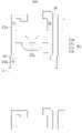
도 1은 일 실시예에 따른 표시 장치의 하나의 화소의 등가 회로도이다.
도 2는 일 실시예에 따른 표시 장치의 복수개의 트랜지스터 및 커패시터의 개략적인 배치도이다.
도 3은 도 2의 구체적인 배치도이다.
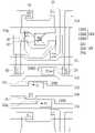
도 4는 도 3의 표시 장치를 IV-IV선을 따라 자른 단면도이다.
도 5는 도 3의 표시 장치를 V-V선, V'-V'선 및 V''-V''선을 따라 자른 단면도이다.
도 6은 도 4의 발광 제어 트랜지스터와 도 5의 보상 트랜지스터를 함께 비교 도시한 단면도이다.
도 7은 도 2에서 다결정 반도체 부재만을 도시한 배치도이다.
도 8은 도 7의 다결정 반도체 부재 위에 제1 게이트 금속선을 적층한 상태를 도시한 배치도이다.
도 9는 도 8의 제1 게이트 금속선 위에 제2 게이트 금속선을 적층한 상태를 도시한 배치도이다.
도 10은 도 9의 제2 게이트 금속선 위에 산화물 반도체 부재를 적층한 상태를 도시한 배치도이다.
도 11은 도 10의 산화물 반도체 부재 위에 제1 데이터 금속선을 적층한 상태를 도시한 배치도이다.
도 12는 도 2 및 도 3의 보상 트랜지스터의 일부 확대도이다.1 is an equivalent circuit diagram of one pixel of a display device according to an exemplary embodiment.
2 is a schematic layout view of a plurality of transistors and capacitors of a display device according to an exemplary embodiment.
FIG. 3 is a detailed layout view of FIG. 2 .
FIG. 4 is a cross-sectional view of the display device of FIG. 3 taken along line IV-IV.
5 is a cross-sectional view of the display device of FIG. 3 taken along lines VV, V'-V', and V''-V''.
6 is a cross-sectional view showing a comparison of the emission control transistor of FIG. 4 and the compensating transistor of FIG. 5 together.
FIG. 7 is a layout view showing only the polycrystalline semiconductor member in FIG. 2 .
FIG. 8 is a layout view illustrating a state in which a first gate metal line is stacked on the polycrystalline semiconductor member of FIG. 7 .
FIG. 9 is a layout view illustrating a state in which a second gate metal line is stacked on the first gate metal line of FIG. 8 .
FIG. 10 is a layout view illustrating a state in which an oxide semiconductor member is stacked on the second gate metal line of FIG. 9 .
FIG. 11 is a layout view illustrating a state in which first data metal lines are stacked on the oxide semiconductor member of FIG. 10 .
12 is an enlarged view of a part of the compensation transistor of FIGS. 2 and 3 .
이하, 첨부한 도면을 참고로 하여 본 발명의 여러 실시예들에 대하여 본 발명이 속하는 기술 분야에서 통상의 지식을 가진 자가 용이하게 실시할 수 있도록 상세히 설명한다. 본 발명은 여러 가지 상이한 형태로 구현될 수 있으며 여기에서 설명하는 실시예들에 한정되지 않는다.Hereinafter, various embodiments of the present invention will be described in detail with reference to the accompanying drawings so that those skilled in the art can easily carry out the present invention. This invention may be embodied in many different forms and is not limited to the embodiments set forth herein.
본 발명을 명확하게 설명하기 위해서 설명과 관계없는 부분은 생략하였으며, 명세서 전체를 통하여 동일 또는 유사한 구성요소에 대해서는 동일한 참조 부호를 붙이도록 한다.In order to clearly describe the present invention, parts irrelevant to the description are omitted, and the same reference numerals are assigned to the same or similar components throughout the specification.
또한, 도면에서 나타난 각 구성의 크기 및 두께는 설명의 편의를 위해 임의로 나타내었으므로, 본 발명이 반드시 도시된 바에 한정되지 않는다. 도면에서 여러 층 및 영역을 명확하게 표현하기 위하여 두께를 확대하여 나타내었다. 그리고 도면에서, 설명의 편의를 위해, 일부 층 및 영역의 두께를 과장되게 나타내었다.In addition, since the size and thickness of each component shown in the drawings are arbitrarily shown for convenience of explanation, the present invention is not necessarily limited to the shown bar. In the drawings, the thickness is shown enlarged to clearly express the various layers and regions. And in the drawings, for convenience of explanation, the thicknesses of some layers and regions are exaggerated.
또한, 명세서 전체에서, 어떤 부분이 어떤 구성요소를 "포함" 한다고 할 때, 이는 특별히 반대되는 기재가 없는 한 다른 구성요소를 제외하는 것이 아니라 다른 구성요소를 더 포함할 수 있는 것을 의미한다. 또한, 명세서 전체에서 층, 막, 영역, 판 등의 부분이 다른 부분 "위에" 또는 "상에" 있다고 할 때, 이는 다른 부분 "바로 위에" 있는 경우뿐 아니라 그 중간에 또 다른 부분이 있는 경우도 포함한다. 또한, "~ 상에" 또는 "~ 위에"라 함은 대상 부분의 위 또는 아래에 위치하는 것을 의미하며, 반드시 중력 방향을 기준으로 상측에 위치하는 것을 의미하지 않는다.In addition, throughout the specification, when a certain component is said to "include", it means that it may further include other components without excluding other components unless otherwise stated. In addition, when a part such as a layer, film, region, plate, etc. is said to be “on” or “on” another part throughout the specification, this is not only when it is “directly on” the other part, but also when there is another part in the middle. Also includes In addition, "on" or "on" means located above or below the target part, and does not necessarily mean located on the upper side relative to the direction of gravity.
또한, 첨부 도면에서 도시된 갯수의 트랜지스터(transistor)와 커패시터(capacitor)에 한정되지 않으며, 표시 장치는 하나의 화소에 복수개의 트랜지스터와 하나 이상의 커패시터를 구비할 수 있으며, 별도의 배선이 더 형성되거나 기존의 배선이 생략되어 다양한 구조를 갖도록 형성할 수도 있다. 여기서, 화소는 화상을 표시하는 최소 단위를 말하며, 표시 장치는 복수의 화소들을 통해 화상을 표시한다.In addition, it is not limited to the number of transistors and capacitors shown in the accompanying drawings, and the display device may include a plurality of transistors and one or more capacitors in one pixel, and a separate wiring is further formed or It may be formed to have various structures by omitting the existing wiring. Here, a pixel refers to a minimum unit for displaying an image, and a display device displays an image through a plurality of pixels.
또한, 명세서 전체에서, "평면상"이라 할 때, 이는 대상 부분을 위에서 보았을 때를 의미하며, "단면상"이라 할 때, 이는 대상 부분을 수직으로 자른 단면을 옆에서 보았을 때를 의미한다.In addition, throughout the specification, when it is referred to as "planar image", it means when the target part is viewed from above, and when it is referred to as "cross-sectional image", it means when a cross section of the target part cut vertically is viewed from the side.
그러면 일 실시예에 따른 표시 장치에 대하여 도면을 참고로 상세하게 설명한다.Then, a display device according to an exemplary embodiment will be described in detail with reference to drawings.
도 1은 일 실시예에 따른 표시 장치의 하나의 화소의 등가 회로도이다.1 is an equivalent circuit diagram of one pixel of a display device according to an exemplary embodiment.
도 1에 도시한 바와 같이, 일 실시예에 따른 표시 장치의 하나의 화소(PX)는 복수개의 신호선(signal line)(151, 152, 153, 154, 155, 156, 171, 172)에 연결되는 복수개의 트랜지스터(transistor)(T1, T2, T3, T4, T5, T6, T7), 스토리지 커패시터(storage capacitor, Cst), 그리고 유기 발광 다이오드(organic light emitting diode, OLED)를 포함할 수 있다. 본 실시예에서는 7개의 트랜지스터와 1개의 커패시터로 이루어진 구조를 도시하고 있지만, 본 실시예가 반드시 이에 한정되는 것은 아니며 트랜지스터의 수와 커패시터의 수는 다양하게 변형 가능하다.As shown in FIG. 1 , one pixel PX of the display device according to an exemplary embodiment is connected to a plurality of
트랜지스터(T1, T2, T3, T4, T5, T6, T7)는 다결정 반도체를 포함하는 제1 트랜지스터(TA)와 산화물 반도체를 포함하는 제2 트랜지스터(TB)를 포함할 수 있다. 제1 트랜지스터(TA)는 구동 트랜지스터(driving transistor)(T1), 스위칭 트랜지스터(switching transistor)(T2), 동작 제어 트랜지스터(operation control transistor)(T5), 그리고 발광 제어 트랜지스터(light emission control transistor)(T6)를 포함할 수 있다. 제2 트랜지스터(TB)는 보상 트랜지스터(compensation transistor)(T3), 초기화 트랜지스터(initialization transistor)(T4), 그리고 바이패스 트랜지스터(bypass transistor)(T7)를 포함할 수 있다.The transistors T1 , T2 , T3 , T4 , T5 , T6 , and T7 may include a first transistor TA including a polycrystalline semiconductor and a second transistor TB including an oxide semiconductor. The first transistor TA includes a driving transistor T1, a switching transistor T2, an operation control transistor T5, and a light emission control transistor ( T6) may be included. The second transistor TB may include a compensation transistor T3, an initialization transistor T4, and a bypass transistor T7.
신호선(151, 152, 153, 154, 155, 156, 171, 172)은 복수개의 제1 스캔선(151), 복수개의 제2 스캔선(152), 복수개의 제3 스캔선(153), 복수개의 발광 제어선(154), 복수개의 바이패스 제어선(155), 복수개의 초기화 전압선(156), 복수개의 데이터선(171), 그리고 복수개의 구동 전압선(172)을 포함할 수 있다. 하나의 화소(PX)에는 하나의 제1 스캔선(151), 하나의 제2 스캔선(152), 하나의 제3 스캔선(153), 하나의 발광 제어선(154), 하나의 바이패스 제어선(155), 하나의 초기화 전압선(156), 하나의 데이터선(171), 그리고 하나의 구동 전압선(172)이 연결될 수 있다.The signal lines 151, 152, 153, 154, 155, 156, 171, and 172 include a plurality of
제1 스캔선(151)은 스위칭 트랜지스터(T2)에 제1 스캔 신호(GW1)를 전달하고, 제2 스캔선(152)은 보상 트랜지스터(T3)에 제2 스캔 신호(GW2)를 전달하며, 제3 스캔선(153)은 초기화 트랜지스터(T4)에 제3 스캔 신호(GI)를 전달할 수 있다. 그리고, 발광 제어선(154)은 동작 제어 트랜지스터(T5) 및 발광 제어 트랜지스터(T6)에 발광 제어 신호(EM)를 전달하고, 바이패스 제어선(155)은 바이패스 트랜지스터(T7)에 바이패스 신호(GB)를 전달할 수 있다. 그리고, 초기화 전압선(156)은 구동 트랜지스터(T1)를 초기화하는 초기화 전압(Vint)을 전달할 수 있다.The
데이터선(171)은 데이터 신호(Dm)를 전달하고, 구동 전압선(172)은 구동 전압(ELVDD)을 전달할 수 있다.The
구동 트랜지스터(T1)의 게이트 전극(G1)은 스토리지 커패시터(Cst)의 일단(Cst1)과 연결되어 있고, 구동 트랜지스터(T1)의 소스 전극(S1)은 동작 제어 트랜지스터(T5)를 경유하여 구동 전압선(172)과 연결되어 있으며, 구동 트랜지스터(T1)의 드레인 전극(D1)은 발광 제어 트랜지스터(T6)를 경유하여 유기 발광 다이오드(OLED)의 애노드(anode)와 전기적으로 연결될 수 있다. 구동 트랜지스터(T1)는 스위칭 트랜지스터(T2)의 스위칭 동작에 따라 데이터 신호(Dm)를 전달받아 유기 발광 다이오드(OLED)에 구동 전류(Id)를 공급할 수 있다.The gate electrode G1 of the driving transistor T1 is connected to one end Cst1 of the storage capacitor Cst, and the source electrode S1 of the driving transistor T1 is a driving voltage line via the operation control transistor T5. 172, and the drain electrode D1 of the driving transistor T1 may be electrically connected to the anode of the organic light emitting diode OLED via the emission control transistor T6. The driving transistor T1 may receive the data signal Dm according to the switching operation of the switching transistor T2 and supply the driving current Id to the organic light emitting diode OLED.
스위칭 트랜지스터(T2)의 게이트 전극(G2)은 제1 스캔선(151)과 연결되어 있고, 스위칭 트랜지스터(T2)의 소스 전극(S2)은 데이터선(171)과 연결되어 있으며, 스위칭 트랜지스터(T2)의 드레인 전극(D2)은 구동 트랜지스터(T1)의 소스 전극(S1)과 연결되어 있으면서 동작 제어 트랜지스터(T5)을 경유하여 구동 전압선(172)과 연결될 수 있다. 이러한 스위칭 트랜지스터(T2)는 제1 스캔선(151)을 통해 전달받은 제1 스캔 신호(GW1)에 따라 턴 온되어 데이터선(171)으로 전달된 데이터 신호(Dm)을 구동 트랜지스터(T1)의 소스 전극(S1)으로 전달하는 스위칭 동작을 수행할 수 있다.The gate electrode G2 of the switching transistor T2 is connected to the
보상 트랜지스터(T3)의 게이트 전극(G3)은 제2 스캔선(152)에 연결되어 있고, 보상 트랜지스터(T3)의 소스 전극(S3)은 구동 트랜지스터(T1)의 드레인 전극(D1)과 연결되어 있으면서 발광 제어 트랜지스터(T6)를 경유하여 유기 발광 다이오드(OLED)의 애노드(anode)와 연결되어 있으며, 보상 트랜지스터(T3)의 드레인 전극(D3)은 초기화 트랜지스터(T4)의 드레인 전극(D4), 스토리지 커패시터(Cst)의 일단(Cst1) 및 구동 트랜지스터(T1)의 게이트 전극(G1)에 함께 연결될 수 있다. 이러한 보상 트랜지스터(T3)는 제2 스캔선(152)을 통해 전달받은 제2 스캔 신호(GW2)에 따라 턴 온되어 구동 트랜지스터(T1)의 게이트 전극(G1)과 드레인 전극(D1)을 서로 연결하여 구동 트랜지스터(T1)를 다이오드 연결시킬 수 있다. 제2 스캔 신호(GW2)는 제1 스캔 신호(GW1)와 레벨이 반전되는 신호로서, 제1 스캔 신호(GW1)가 하이 레벨(high level)이면, 제2 스캔 신호(GW2)는 로우 레벨(low level)이고, 제1 스캔 신호(GW1)가 로우 레벨(low level)이면, 제2 스캔 신호(GW2)는 하이 레벨(high level)일 수 있다.The gate electrode G3 of the compensation transistor T3 is connected to the
초기화 트랜지스터(T4)의 게이트 전극(G4)은 제3 스캔선(153)과 연결되어 있고, 초기화 트랜지스터(T4)의 소스 전극(S4)은 초기화 전압선(156)과 연결되어 있으며, 초기화 트랜지스터(T4)의 드레인 전극(D4)은 보상 트랜지스터(T3)의 드레인 전극(D3)을 거쳐 스토리지 커패시터(Cst)의 일단(Cst1) 및 구동 트랜지스터(T1)의 게이트 전극(G1)에 함께 연결될 수 있다. 이러한 초기화 트랜지스터(T4)는 제3 스캔선(153)을 통해 전달받은 제3 스캔 신호(GI)에 따라 턴 온되어 초기화 전압(Vint)을 구동 트랜지스터(T1)의 게이트 전극(G1)에 전달하여 구동 트랜지스터(T1)의 게이트 전극(G1)의 게이트 전압(Vg)을 초기화시키는 초기화 동작을 수행할 수 있다.The gate electrode G4 of the initialization transistor T4 is connected to the
동작 제어 트랜지스터(T5)의 게이트 전극(G5)은 발광 제어선(154)과 연결되어 있으며, 동작 제어 트랜지스터(T5)의 소스 전극(S5)은 구동 전압선(172)와 연결되어 있고, 동작 제어 트랜지스터(T5)의 드레인 전극(D5)은 구동 트랜지스터(T1)의 소스 전극(S1) 및 스위칭 트랜지스터(T2)의 드레인 전극(D2)에 연결될 수 있다.The gate electrode G5 of the operation control transistor T5 is connected to the
발광 제어 트랜지스터(T6)의 게이트 전극(G6)은 발광 제어선(154)과 연결되어 있으며, 발광 제어 트랜지스터(T6)의 소스 전극(S6)은 구동 트랜지스터(T1)의 드레인 전극(D1) 및 보상 트랜지스터(T3)의 소스 전극(S3)과 연결되어 있고, 발광 제어 트랜지스터(T6)의 드레인 전극(D6)은 유기 발광 다이오드(OLED)의 애노드(anode)와 전기적으로 연결될 수 있다. 이러한 동작 제어 트랜지스터(T5) 및 발광 제어 트랜지스터(T6)는 발광 제어선(154)을 통해 전달받은 발광 제어 신호(EM)에 따라 동시에 턴 온되고 이를 통해 구동 전압(ELVDD)이 다이오드 연결된 구동 트랜지스터(T1)를 통해 보상되어 유기 발광 다이오드(OLED)에 전달될 수 있다.The gate electrode G6 of the light emitting control transistor T6 is connected to the light emitting
바이패스 트랜지스터(T7)의 게이트 전극(G7)은 바이패스 제어선(155)과 연결되어 있고, 바이패스 트랜지스터(T7)의 소스 전극(S7)은 발광 제어 트랜지스터(T6)의 드레인 전극(D6) 및 유기 발광 다이오드(OLED)의 애노드에 함께 연결되어 있고, 바이패스 트랜지스터(T7)의 드레인 전극(D7)은 초기화 전압선(156) 및 초기화 트랜지스터(T4)의 소스 전극(S4)에 함께 연결될 수 있다.The gate electrode G7 of the bypass transistor T7 is connected to the
스토리지 커패시터(Cst)의 타단(Cst2)은 구동 전압선(172)과 연결되어 있으며, 유기 발광 다이오드(OLED)의 캐소드(cathode)는 공통 전압(ELVSS)을 전달하는 공통 전압선(741)과 연결될 수 있다.The other end Cst2 of the storage capacitor Cst is connected to the driving
이 때, 구동 트랜지스터(T1), 스위칭 트랜지스터(T2), 동작 제어 트랜지스터(T5), 그리고 발광 제어 트랜지스터(T6)를 포함하는 제1 트랜지스터(TA)는 PMOS (P-channel metal oxide semiconductor) 구조의 트랜지스터로 구성될 수 있다. 그리고, 보상 트랜지스터(T3), 초기화 트랜지스터(T4) 및 바이패스 트랜지스터(T7)를 포함하는 제2 트랜지스터(TB)는 NMOS (N-channel metal oxide semiconductor) 구조의 트랜지스터로 구성될 수 있다.At this time, the first transistor TA including the driving transistor T1, the switching transistor T2, the operation control transistor T5, and the emission control transistor T6 has a P-channel metal oxide semiconductor (PMOS) structure. It can be made of transistors. Also, the second transistor TB including the compensation transistor T3, the initialization transistor T4, and the bypass transistor T7 may be configured as an N-channel metal oxide semiconductor (NMOS) structure transistor.
이하에서, 도 1에 도시한 표시 장치의 상세 구조에 대하여 도 2 내지 도 12를 참고하여 상세하게 설명한다.Hereinafter, a detailed structure of the display device shown in FIG. 1 will be described in detail with reference to FIGS. 2 to 12 .
도 2는 일 실시예에 따른 표시 장치의 복수개의 트랜지스터 및 커패시터의 개략적인 배치도이고, 도 3은 도 2의 구체적인 배치도이다. 그리고, 도 4는 도 3의 표시 장치를 IV-IV선을 따라 자른 단면도이고, 도 5는 도 3의 표시 장치를 V-V선, V'-V'선 및 V''-V''선을 따라 자른 단면도이며, 도 6은 도 4의 발광 제어 트랜지스터와 도 5의 보상 트랜지스터를 함께 비교 도시한 단면도이다.FIG. 2 is a schematic layout view of a plurality of transistors and capacitors of a display device according to an exemplary embodiment, and FIG. 3 is a detailed layout view of FIG. 2 . 4 is a cross-sectional view of the display device of FIG. 3 taken along line IV-IV, and FIG. 5 is a cross-sectional view of the display device of FIG. 3 taken along lines V-V, V'-V', and V''-V''. 6 is a cross-sectional view showing a comparison between the emission control transistor of FIG. 4 and the compensating transistor of FIG. 5 .
그리고, 도 7은 도 2에서 다결정 반도체 부재만을 도시한 배치도이고, 도 8은 도 7의 다결정 반도체 부재 위에 제1 게이트 금속선을 적층한 상태를 도시한 배치도이다. 그리고, 도 9는 도 8의 제1 게이트 금속선 위에 제2 게이트 금속선을 적층한 상태를 도시한 배치도이며, 도 10은 도 9의 제2 게이트 금속선 위에 산화물 반도체 부재를 적층한 상태를 도시한 배치도이고, 도 11은 도 10의 산화물 반도체 부재 위에 제1 데이터 금속선을 적층한 상태를 도시한 배치도이다.Further, FIG. 7 is a layout view showing only the polycrystalline semiconductor member in FIG. 2 , and FIG. 8 is a layout view showing a state in which a first gate metal line is stacked on the polycrystalline semiconductor member of FIG. 7 . Further, FIG. 9 is a layout view showing a state in which a second gate metal line is stacked on the first gate metal line in FIG. 8 , and FIG. 10 is a layout view showing a state in which an oxide semiconductor member is stacked on the second gate metal line in FIG. 9 . , FIG. 11 is a layout view illustrating a state in which first data metal lines are stacked on the oxide semiconductor member of FIG. 10 .
이하에서 도면을 참고하여 일 실시예에 따른 표시 장치의 구체적인 평면상 구조 및 단면상 구조에 대해 상세히 설명한다.Hereinafter, a specific planar structure and a cross-sectional structure of a display device according to an exemplary embodiment will be described in detail with reference to drawings.
우선, 도 2 및 도 3에 도시한 바와 같이, 일 실시예에 따른 표시 장치는 제1 스캔 신호(GW1), 제2 스캔 신호(GW2), 제3 스캔 신호(GI), 발광 제어 신호(EM), 그리고 바이패스 신호(GB)를 각각 인가하며 행 방향을 따라 연장되는 제1 스캔선(151), 제2 스캔선(152), 제3 스캔선(153), 발광 제어선(154), 그리고 바이패스 제어선(155)을 포함한다. 그리고, 초기화 전압(Vint)은 초기화 전압선(156)에서 초기화 트랜지스터(T4)를 경유하여 보상 트랜지스터(T3)로 전달된다.First, as shown in FIGS. 2 and 3 , the display device according to an exemplary embodiment includes a first scan signal GW1 , a second scan signal GW2 , a third scan signal GI, and an emission control signal EM. ), and the
그리고, 화소(PX)에 데이터 신호(Dm) 및 구동 전압(ELVDD)을 각각 인가하는 데이터선(171) 및 구동 전압선(172)을 포함한다. 구동 전압선(172)은 제1 방향인 행 방향을 따라 연장되며 데이터선(171)에 평행한 제1 구동 전압선(172a)과, 제2 방향인 열 방향을 따라 연장되며 제1 스캔선(151)에 평행한 제2 구동 전압선(172b)을 포함할 수 있다. 제1 구동 전압선(172a)과 제2 구동 전압선(172b)은 접촉 구멍(68)을 통해 서로 연결될 수 있다. 따라서, 열 방향으로 길게 연장된 제1 구동 전압선(172a)만 형성되어 구동 전압을 전달하는 경우에 비해, 본 실시예는 열 방향으로 길게 연장된 제1 구동 전압선(172a)과 행 방향으로 길게 연장된 제2 구동 전압선(172b)을 접촉 구멍(68)을 통해 서로 연결함으로써 메쉬(mesh) 구조를 형성할 수 있으므로, 구동 전압선(172)의 전압 강하를 최소화할 수 있다.In addition, a
또한, 화소(PX)에는 구동 트랜지스터(T1), 스위칭 트랜지스터(T2), 보상 트랜지스터(T3), 초기화 트랜지스터(T4), 동작 제어 트랜지스터(T5), 발광 제어 트랜지스터(T6), 바이패스 트랜지스터(T7), 스토리지 커패시터(Cst), 그리고 유기 발광 다이오드(OLED)가 위치할 수 있다.In addition, the pixel PX includes a driving transistor T1, a switching transistor T2, a compensation transistor T3, an initialization transistor T4, an operation control transistor T5, an emission control transistor T6, and a bypass transistor T7. ), a storage capacitor Cst, and an organic light emitting diode OLED may be positioned.
유기 발광 다이오드(OLED)는 화소 전극(191), 유기 발광층(370) 및 공통 전극(270)을 포함할 수 있다.The organic light emitting diode (OLED) may include a
구동 트랜지스터(T1), 스위칭 트랜지스터(T2), 동작 제어 트랜지스터(T5), 그리고 발광 제어 트랜지스터(T6)는 트랜지스터 온 구동 시, 전류가 흐르게 되는 제1 채널(first channel)(30a)을 가진다.The driving transistor T1, the switching transistor T2, the operation control transistor T5, and the emission control transistor T6 have a first channel 30a through which current flows when the transistor is turned on.
도 7에 도시한 바와 같이, 하나의 다결정 반도체 부재(130A)의 내부에 제1 채널(30a)이 형성되어 있으며, 다결정 반도체 부재(130A)는 다양한 형상으로 굴곡될 수 있다. 이러한 다결정 반도체 부재(130A)는 다결정 실리콘(polycystalline silicon)을 포함할 수 있다.As shown in FIG. 7 , the first channel 30a is formed inside one
제1 채널(30a)은 구동 트랜지스터(T1)에 위치하는 구동 채널(131a), 스위칭 트랜지스터(T2)에 위치하는 스위칭 채널(131b), 동작 제어 트랜지스터(T5)에 위치하는 동작 제어 채널(131e), 발광 제어 트랜지스터(T6)에 위치하는 발광 제어 채널(131f)을 포함할 수 있다.The first channel 30a includes a driving
다결정 반도체 부재(130A)는 불순물로 채널 도핑이 되어 있는 제1 채널 (30a)과, 채널의 양 옆에 형성되어 있으며 채널에 도핑된 도핑 불순물보다 도핑 농도가 높은 소스 도핑 영역 및 드레인 도핑 영역을 포함할 수 있다. 본 실시예에서 다결정 반도체 부재 내에 형성된 소스 도핑 영역 및 드레인 도핑 영역은 각각 소스 전극 및 드레인 전극에 해당할 수 있다. 예컨대, 스위칭 채널(131b)의 양 옆에 소스 전극(S2) 및 드레인 전극(D2)이 위치할 수 있으며, 다른 채널들의 양 옆에도 동일한 구조로 소스 전극 및 드레인 전극이 위치할 수 있다. 다결정 반도체 부재(130A)에 형성되어 있는 소스 전극 및 드레인 전극은 해당 영역만 도핑하여 형성할 수 있다. 또한, 다결정 반도체 부재(130A)에서 서로 다른 트랜지스터의 소스 전극과 드레인 전극의 사이 영역도 도핑되어 소스 전극과 드레인 전극이 전기적으로 연결될 수 있다.The
구동 트랜지스터(T1)는 구동 채널(131a), 구동 게이트 전극(155a), 구동 소스 전극(136a) 및 구동 드레인 전극(137a)을 포함한다. 구동 채널(131a)은 굴곡되어 있으며, 'U'자 형상을 가질 수 있다. 그러나, 반드시 이에 한정되는 것은 아니며, 구동 채널(131a)의 형상은 사행 형상(meandering shape), 지그재그 형상(zigzag shape), '역S', 'S', 'M', 'W' 등의 다양한 형상이 가능하다. 이와 같이, 굴곡된 형상의 구동 채널(131a)을 형성함으로써, 좁은 공간 내에 길게 구동 채널(131a)을 형성할 수 있다. 따라서, 길게 형성된 구동 채널(131a)에 의해 구동 게이트 전극(155a)과 구동 소스 전극(136a) 간의 구동 게이트-소스 전압(Vgs)의 구동 범위(driving range)는 넓어지게 된다. 구동 게이트-소스 전압(Vgs)의 구동 범위가 넓으므로 구동 게이트-소스 전압(Vgs)의 크기를 변화시켜 유기 발광 다이오드(OLED)에서 방출되는 빛의 계조를 보다 세밀하게 제어할 수 있으며, 그 결과 유기 발광 표시 장치의 해상도를 높이고 표시 품질을 향상시킬 수 있다.The driving transistor T1 includes a driving
구동 게이트 전극(155a)은 구동 채널(131a)과 중첩하고 있으며, 구동 소스 전극(136a) 및 구동 드레인 전극(137a)은 구동 채널(131a)의 양 옆에 인접하여 각각 형성되어 있다. 구동 게이트 전극(155a)은 접촉 구멍(61)을 통해 제1 연결 부재(173)의 일단부(173a)와 연결되어 있다. 이러한 구동 트랜지스터(T1)는 구동 게이트 전극(155a)이 구동 채널(131a) 위에 위치하는 탑 게이트 구조를 가진다.The driving
스위칭 트랜지스터(T2)는 스위칭 채널(131b), 스위칭 게이트 전극(155b), 스위칭 소스 전극(136b) 및 스위칭 드레인 전극(137b)을 포함한다. 제1 스캔선(151)의 일부인 스위칭 게이트 전극(155b)은 스위칭 채널(131b)과 중첩하고 있으며, 스위칭 소스 전극(136b) 및 스위칭 드레인 전극(137b)은 스위칭 채널(131b)의 양 옆에 인접하여 각각 형성될 수 있다. 스위칭 소스 전극(136b)은 접촉 구멍(62)을 통해 데이터선(171)과 연결될 수 있다. 이러한 스위칭 트랜지스터(T2)는 스위칭 게이트 전극(155b)이 스위칭 채널(131b) 위에 위치하는 탑 게이트 구조를 가진다.The switching transistor T2 includes a switching
동작 제어 트랜지스터(T5)는 동작 제어 채널(131e), 동작 제어 게이트 전극(155e), 동작 제어 소스 전극(136e) 및 동작 제어 드레인 전극(137e)을 포함한다. 발광 제어선(154)의 일부인 동작 제어 게이트 전극(155e)은 동작 제어 채널(131e)과 중첩하고 있으며, 동작 제어 소스 전극(136e) 및 동작 제어 드레인 전극(137e)은 동작 제어 채널(131e)의 양 옆에 인접하여 각각 형성될 수 있다. 동작 제어 소스 전극(136e)은 접촉 구멍(65)을 통해 제1 구동 전압선(172a)과 연결될 수 있다.The operation control transistor T5 includes an
이러한 동작 제어 트랜지스터(T5)는 동작 제어 게이트 전극(155e)이 동작 제어 채널(131e) 위에 위치하는 탑 게이트 구조를 가진다.The operation control transistor T5 has a top gate structure in which the operation control gate electrode 155e is positioned over the
발광 제어 트랜지스터(T6)는 발광 제어 채널(131f), 발광 제어 게이트 전극(155f), 발광 제어 소스 전극(136f) 및 발광 제어 드레인 전극(137f)을 포함한다. 발광 제어선(154)의 일부인 발광 제어 게이트 전극(155f)은 발광 제어 채널(131f)과 중첩하고 있으며, 발광 제어 소스 전극(136f) 및 발광 제어 드레인 전극(137f)은 발광 제어 채널(131f)의 양 옆에 인접하여 각각 형성될 수 있다. 발광 제어 드레인 전극(137f)은 접촉 구멍(66)을 통해 제4 연결 부재(176)와 연결될 수 있다.The emission control transistor T6 includes an
구동 트랜지스터(T1)의 구동 채널(131a)의 일단은 스위칭 드레인 전극(137b) 및 동작 제어 드레인 전극(137e)과 연결되며, 구동 채널(131a)의 타단은 발광 제어 소스 전극(136f)과 연결될 수 있다.One end of the driving
이러한 발광 제어 트랜지스터(T6)는 발광 제어 게이트 전극(155f)이 발광 제어 채널(131f) 위에 위치하는 탑 게이트 구조를 가진다.The emission control transistor T6 has a top gate structure in which the emission
구동 게이트 전극(155a), 스위칭 게이트 전극(155b), 동작 제어 게이트 전극(155e), 및 발광 제어 게이트 전극(155f)은 제1 게이트 전극을 이룬다. 구동 소스 전극(136a), 스위칭 소스 전극(136b), 동작 제어 소스 전극(136e), 및 발광 제어 소스 전극(136f)은 제1 소스 전극을 이루며, 구동 드레인 전극(137a), 스위칭 드레인 전극(137b), 동작 제어 드레인 전극(137e), 및 발광 제어 드레인 전극(137f)은 제1 드레인 전극을 이룬다.The driving
한편, 다결정 반도체로 이루어진 트랜지스터를 포함하는 표시 장치는 플리커(flicker) 문제로 30Hz 이하의 저주파로 구동하기 어려웠다. 따라서, 다결정 반도체를 포함하는 트랜지스터를 포함하는 표시 장치는 플리커 발생을 최소화하기 위해 고주파로 구동하여야 하므로, 소비 전력이 증가하였다.Meanwhile, a display device including a transistor made of a polycrystalline semiconductor is difficult to drive at a low frequency of 30 Hz or less due to a flicker problem. Accordingly, since a display device including a transistor including a polycrystalline semiconductor needs to be driven at a high frequency to minimize flicker, power consumption is increased.
따라서, 본 실시예에서 제1 트랜지스터(TA)는 다결정 반도체로 형성하고, 제2 트랜지스터(TB)는 저주파 구동이 가능한 산화물 반도체로 형성함으로써, 플리커 발생을 최소화하는 동시에 소비 전력을 저감시킬 수 있다.Therefore, in the present embodiment, the first transistor TA is formed of a polycrystalline semiconductor and the second transistor TB is formed of an oxide semiconductor capable of low-frequency driving, thereby minimizing flicker and reducing power consumption.
본 실시예의 산화물 반도체를 포함하는 제2 트랜지스터(TB)는 바텀 게이트 구조를 가질 수 있다. 바텀 게이트 구조는 탑 게이트 구조에 비해 채널을 짧게 형성할 수 있고, 접촉 구멍의 수를 감소시킬 수 있는 장점이 있다.The second transistor TB including the oxide semiconductor according to the present embodiment may have a bottom gate structure. Compared to the top gate structure, the bottom gate structure has advantages in that a channel can be formed shorter and the number of contact holes can be reduced.
이러한 바텀 게이트 구조의 제2 트랜지스터(TB)인 보상 트랜지스터(T3), 초기화 트랜지스터(T4), 및 바이패스 트랜지스터(T7)는 트랜지스터 온 구동 시, 전류가 흐르게 되는 제2 채널(second channel)(30b)을 가진다.The compensation transistor T3, the initialization transistor T4, and the bypass transistor T7, which are the second transistors TB of the bottom gate structure, form a
산화물 반도체로 이루어지는 제2 채널(30b)은 상부가 외부로 노출되므로 외광에 의해 누설 전류가 발생하기 쉽다. 따라서, 본 실시예에서는 제2 채널(30b)과 중첩하는 위치에 외광 차단 부재(70)를 위치시킴으로써, 외광에 의한 누설 전류의 발생을 최소화할 수 있다.Since the top of the
제2 채널(30b)은 제1 산화물 반도체 부재(130B1)의 내부에 위치하는 보상 채널(131c), 제2 산화물 반도체 부재(130B2)의 내부에 위치하는 초기화 채널(131d), 그리고 제3 산화물 반도체 부재(130B3)의 내부에 위치하는 바이패스 채널(131g)을 포함할 수 있다.The
외광 차단 부재(70)는 제1 구동 전압선(172a)으로부터 연장되어 형성되며, 보상 채널(131c)과 중첩하는 제1 차단 부재(71), 초기화 채널(131d)과 중첩하는 제2 차단 부재(72), 바이패스 채널(131g)과 중첩하는 제3 차단 부재(73)를 포함할 수 있다. 외광 차단 부재(70)의 구체적인 내용은 이하에서 후술한다.The external light blocking member 70 extends from the first
도 10에 도시한 바와 같이, 서로 분리된 산화물 반도체 부재(130B)의 내부에 제2 채널(30b)이 형성되어 있으며, 각각의 산화물 반도체 부재(130B)는 사각 형상을 가진다. 그러나, 산화물 반도체 부재(130B)의 형상은 이에 반드시 한정되는 것을 아니며 다양한 형상으로 변형이 가능하다. 산화물 반도체 부재(130B)는 보상 트랜지스터(T3)에 위치하는 제1 산화물 반도체 부재(130B1), 초기화 트랜지스터(T4)에 위치하는 제2 산화물 반도체 부재(130B2), 그리고 바이패스 트랜지스터(T7)에 위치하는 제3 산화물 반도체 부재(130B3)을 포함할 수 있다.As shown in FIG. 10 ,
이러한 산화물 반도체 부재(130B)는 산화물 반도체를 포함할 수 있다. 산화물 반도체는 아연(Zn), 인듐(In), 갈륨(Ga), 주석(Sn), 티타늄(Ti) 등의 금속의 산화물, 또는 아연(Zn), 인듐(In), 갈륨(Ga), 주석(Sn), 티타늄(Ti) 등의 금속과 이들의 산화물의 조합을 포함할 수 있다. 좀더 구체적으로, 산화물은 산화 아연(ZnO), 아연-주석 산화물(ZTO), 아연-인듐 산화물(ZIO), 인듐 산화물(InO), 티타늄 산화물(TiO), 인듐-갈륨-아연 산화물(IGZO), 인듐-아연-주석 산화물(IZTO) 중 적어도 하나를 포함할 수 있다.The
보상 트랜지스터(T3)는 보상 채널(131c), 보상 게이트 전극(155c), 보상 소스 전극(136c) 및 보상 드레인 전극(137c)을 포함한다. 이러한 보상 트랜지스터(T3)는 보상 게이트 전극(155c)이 보상 채널(131c) 아래에 위치하는 바텀 게이트 구조를 가진다.The compensation transistor T3 includes a
제2 스캔선(152)의 일부인 보상 게이트 전극(155c)은 제1 산화물 반도체 부재(130B1)와 중첩할 수 있다. 보상 소스 전극(136c)은 제2 연결 부재(174)의 일단부이고, 보상 드레인 전극(137c)은 제1 연결 부재(173)의 중간부에 해당한다.The
보상 소스 전극(136c) 및 보상 드레인 전극(137c)은 제1 산화물 반도체 부재(130B)와 평면상 일부 중첩한다. 제1 산화물 반도체 부재(130B) 중 보상 소스 전극(136c) 및 보상 드레인 전극(137c)과 중첩하지 않는 부분은 보상 채널(131c)을 형성할 수 있다. 따라서, 보상 채널(131c)은 외부로 노출되므로, 외광에 의해 누설 전류가 발생하기 쉽다. 보상 채널(131c)과 중첩하는 제1 차단 부재(71)가 제1 구동 전압선(172a)으로부터 연장되어 위치한다. 이러한 제1 차단 부재(71)는 외광이 보상 채널(131c)에 전달되는 것을 차단시킬 수 있으므로, 외광에 의한 누설 전류의 발생을 최소화할 수 있다.The
제2 연결 부재(174)의 타단부(174a)는 접촉 구멍(63)을 통해 구동 드레인 전극(137a)과 연결될 수 있다.The
초기화 트랜지스터(T4)는 초기화 채널(131d), 초기화 게이트 전극(155d), 초기화 소스 전극(136d) 및 초기화 드레인 전극(137d)을 포함한다. 이러한 초기화 트랜지스터(T4)는 초기화 게이트 전극(155d)이 초기화 채널(131d) 아래에 위치하는 바텀 게이트 구조를 가진다. 제3 스캔선(153)의 일부인 초기화 게이트 전극(155d)은 초기화 채널(131d)과 중첩할 수 있다. 초기화 소스 전극(136d)은 제3 연결 부재(175)의 일단부에 해당하고, 초기화 드레인 전극(137d)은 제1 연결 부재(173)의 타단부에 해당한다.The initialization transistor T4 includes an
초기화 소스 전극(136d) 및 초기화 드레인 전극(137d)은 제2 산화물 반도체 부재(130B2)와 평면상 일부 중첩한다. 제2 산화물 반도체 부재(130B2) 중 초기화 소스 전극(136d) 및 초기화 드레인 전극(137d)과 중첩하지 않는 부분은 초기화 채널(131d)을 형성할 수 있다. 따라서, 초기화 채널(131d)은 외부로 노출되므로, 외광에 의해 누설 전류가 발생하기 쉽다. 초기화 채널(131d)과 중첩하는 제2 차단 부재(72)가 제1 구동 전압선(172a)으로부터 연장되어 위치한다. 이러한 제2 차단 부재(72)는 외광이 초기화 채널(131d)에 전달되는 것을 차단시킬 수 있으므로, 외광에 의한 누설 전류의 발생을 최소화할 수 있다.The
제3 연결 부재(175)의 중간부(175a)는 접촉 구멍(64)을 통해 초기화 전압선(156)과 연결될 수 있다.The
바이패스 트랜지스터(T7)는 바이패스 채널(131g), 바이패스 게이트 전극(155g), 바이패스 소스 전극(136g) 및 바이패스 드레인 전극(137g)을 포함한다. 이러한 바이패스 트랜지스터(T7)는 바이패스 게이트 전극(155g)이 바이패스 채널(131g) 아래에 위치하는 바텀 게이트 구조를 가진다.The bypass transistor T7 includes a
바이패스 제어선(155)의 일부인 바이패스 게이트 전극(155g)은 제3 산화물 반도체 부재(130B3)와 중첩할 수 있다.The
제4 연결 부재(176)의 일단부는 바이패스 소스 전극(136g)에 해당하고, 제4 연결 부재(176)의 타단부(176a)는 제6 연결 부재(74)와 접촉 구멍(81)을 통해 연결될 수 있다. 제6 연결 부재(74)는 접촉 구멍(83)을 통해 화소 전극(191)과 연결될 수 있다.One end of the fourth connecting
바이패스 소스 전극(136g) 및 바이패스 드레인 전극(137g)은 제3 산화물 반도체 부재(130B3)와 평면상 일부 중첩한다. 제3 산화물 반도체 부재(130B3) 중 바이패스 소스 전극(136g) 및 바이패스 드레인 전극(137g)과 중첩하지 않는 부분은 바이패스 채널(131g)을 형성할 수 있다. 따라서, 바이패스 채널(131g)은 외부로 노출되므로, 외광에 의해 누설 전류가 발생하기 쉽다. 바이패스 채널(131g)과 중첩하는 제3 차단 부재(73)가 제1 구동 전압선(172a)으로부터 연장되어 위치한다. 이러한 제3 차단 부재(73)는 외광이 바이패스 채널(131g)에 전달되는 것을 차단시킬 수 있으므로, 외광에 의한 누설 전류의 발생을 최소화할 수 있다.The
바이패스 소스 전극(136g)은 접촉 구멍(66)을 통해 발광 제어 드레인 전극(137f)과 연결될 수 있고, 바이패스 드레인 전극(137g)은 초기화 소스 전극(136d)과 직접 연결될 수 있다.The
여기서, 보상 게이트 전극(155c), 초기화 게이트 전극(155d), 바이패스 게이트 전극(155g)은 제2 게이트 전극을 이룬다. 보상 소스 전극(136c), 초기화 소스 전극(136d) 및 바이패스 소스 전극(136g)은 제2 소스 전극을 이루며, 보상 드레인 전극(137c), 초기화 드레인 전극(137d) 및 바이패스 드레인 전극(137g)은 제2 드레인 전극을 이룬다.Here, the
도 9에 도시한 바와 같이, 스토리지 커패시터(Cst)는 제2 게이트 절연막(142)를 사이에 두고 서로 중첩하는 제1 스토리지 전극(155a)과 제2 스토리지 전극(172b)을 포함한다. 제1 스토리지 전극(155a)은 구동 게이트 전극(155a)에 해당하고, 제2 스토리지 전극(172b)은 제2 구동 전압선(172b)에서 확장된 부분으로서, 구동 게이트 전극(155a)보다 넓은 면적을 차지하며 구동 게이트 전극(155a)을 전부 덮고 있다.As shown in FIG. 9 , the storage capacitor Cst includes a
여기서, 제2 게이트 절연막(142)은 유전체가 되며, 스토리지 커패시터(Cst)에서 축전된 전하와 양 스토리지 전극(155a, 172b) 사이의 전압에 의해 스토리지 커패시턴스(Storage Capacitance)가 결정된다. 이와 같이, 구동 게이트 전극(155a)을 제1 스토리지 전극(155a)으로 사용함으로써, 화소 내에서 큰 면적을 차지하는 구동 채널(131a)에 의해 좁아진 공간에서 스토리지 커패시터를 형성할 수 있는 공간을 확보할 수 있다.Here, the second
구동 게이트 전극(155a)인 제1 스토리지 전극(155a)은 접촉 구멍(61) 및 스토리지 개구부(51)를 통하여 제1 연결 부재(173)의 일단부와 연결될 수 있다. 스토리지 개구부(51)는 제2 스토리지 전극(172b)에 형성된 개구부이다. 따라서, 스토리지 개구부(51) 내부에 제1 연결 부재(173)의 일단부(173a)와 구동 게이트 전극(155a)을 연결하는 접촉 구멍(61)이 형성되어 있다. 제1 연결 부재(173)는 데이터선(171)과 거의 평행하게 동일한 층에 형성되어 있으며 제1 연결 부재(173)의 중간부는 보상 트랜지스터(T3)의 보상 드레인 전극(137c)에 해당하고, 제1 연결 부재의 타단부는 초기화 트랜지스터(T4)의 초기화 드레인 전극(137d)에 해당한다.The
따라서, 제1 연결 부재(173)는 구동 게이트 전극(155a)과 보상 트랜지스터(T3)의 보상 드레인 전극(137c) 및 초기화 트랜지스터(T4)의 초기화 드레인 전극(137d)을 서로 연결하고 있다.Accordingly, the first connecting
제2 스토리지 전극(172b)은 접촉 구멍(68)을 통해 제5 연결 부재(178)의 일단부(178a)와 연결될 수 있다. 제5 연결 부재(178)의 타단부(178b)는 접촉 구멍(82)을 통해 제1 구동 전압선(172a)과 연결될 수 있다. 따라서, 스토리지 커패시터(Cst)는 제1 구동 전압선(172a)을 통해 제2 스토리지 전극(172b)에 전달된 구동 전압(ELVDD)과 구동 게이트 전극(155a)의 구동 게이트 전압(Vg)간의 차에 대응하는 스토리지 커패시턴스를 저장한다.The
이하, 도 4 및 도 5를 참고하여 일 실시예에 따른 표시 장치의 단면상 구조에 대해 적층 순서에 따라 구체적으로 설명한다. Hereinafter, a cross-sectional structure of a display device according to an exemplary embodiment will be described in detail according to a stacking order with reference to FIGS. 4 and 5 .
기판(110) 위에는 버퍼층(120)이 위치할 수 있다. 기판(110)은 유리, 석영, 세라믹, 플라스틱 등으로 이루어진 절연성 기판으로 형성될 수 있고, 버퍼층(120)은 다결정 규소를 형성하기 위한 결정화 공정 시 기판(110)으로부터 불순물을 차단하여 다결정 규소의 특성을 향상시키고, 기판(110)이 받는 스트레스를 줄이는 역할을 할 수 있다.A
버퍼층(120) 위에는 구동 채널(131a), 스위칭 채널(131b), 동작 제어 채널(131e), 그리고 발광 제어 채널(131f)이 형성된 다결정 반도체 부재(130A)가 위치할 수 있다.A
다결정 반도체 부재(130A) 중 구동 채널(131a)의 양 옆에는 구동 소스 전극(136a) 및 구동 드레인 전극(137a)이 위치하고, 스위칭 채널(131b)의 양 옆에는 스위칭 소스 전극(136b) 및 스위칭 드레인 전극(137b)이 위치할 수 있다.Of the
그리고, 동작 제어 채널(131e)의 양 옆에는 동작 제어 소스 전극(136e) 및 동작 제어 드레인 전극(137e)이 위치하고, 발광 제어 채널(131f)의 양 옆에는 발광 제어 소스 전극(136f) 및 발광 제어 드레인 전극(137f)이 위치할 수 있다.Further, the motion
다결정 반도체 부재(130A) 위에는 이를 덮는 제1 게이트 절연막(141)이 위치할 수 있다. 제1 게이트 절연막(141)은 제1 절연층일 수 있다.A first
도 8에 도시한 바와 같이, 제1 게이트 절연막(141) 위에는 스위칭 게이트 전극(155b)을 포함하는 제1 스캔선(151), 동작 제어 게이트 전극(155e) 및 발광 제어 게이트 전극(155f)을 포함하는 발광 제어선(154), 그리고 초기화 전압선(156)을 포함하는 제1 게이트 금속선(151, 154, 156, 155a)이 위치할 수 있다.As shown in FIG. 8 , a
제1 게이트 금속선(151, 154, 156, 155a) 및 제1 게이트 절연막(141) 위에는 이를 덮는 제2 게이트 절연막(142)이 위치할 수 있다. 제1 게이트 절연막(141) 및 제2 게이트 절연막(142)은 질화 규소(SiNx) 또는 산화 규소(SiO2) 따위로 형성될 수 있다.A second
도 9에 도시한 바와 같이, 제2 게이트 절연막(142) 위에는 제2 구동 전압선(172b), 보상 게이트 전극(155c)을 포함하는 제2 스캔선(152), 초기화 게이트 전극(155d)을 제3 스캔선(153), 바이패스 게이트 전극(155g)을 포함하는 바이패스 제어선(155)을 포함하는 제2 게이트 금속선(172b, 152, 153, 155)이 위치할 수 있다.As shown in FIG. 9 , the second
제1 게이트 금속선(151, 154, 156, 155a)과 제2 게이트 금속선(172b, 152, 153, 155)을 포함하는 게이트 금속선(151, 154, 156, 155a, 172b, 152, 153, 155)은 구리(Cu), 구리 합금, 알루미늄(Al), 알루미늄 합금, 몰리브덴(Mo), 및 몰리브덴 합금 중 어느 하나를 포함하는 금속막이 적층된 다중막으로 형성될 수 있다. 그러나, 제1 게이트 금속선(151, 154, 156, 155a)과 제2 게이트 금속선(172b, 152, 153, 155)이 반드시 동일한 물질로 형성되는 것은 아니며, 서로 다른 물질로 형성될 수도 있다.The
제2 게이트 절연막(142) 및 제2 게이트 금속선(172b, 152, 153, 155) 위에는 층간 절연막(160)이 위치할 수 있다. 층간 절연막(160)은 질화 규소(SiNx) 또는 산화 규소(SiO2) 따위로 형성될 수 있다.An interlayer insulating
도 10에 도시한 바와 같이, 층간 절연막(160)에는 접촉 구멍(61, 62, 63, 64, 65, 66, 68)이 형성될 수있다. 층간 절연막(160) 위에는 보상 채널(131c), 초기화 채널(131d), 및 바이패스 채널(131g)이 각각 형성된 제1 산화물 반도체 부재(130B1), 제2 산화물 반도체 부재(130B2) 및 제3 산화물 반도체 부재(130B3)를 포함하는 산화물 반도체 부재(130B)가 위치할 수 있다.As shown in FIG. 10 , contact holes 61 , 62 , 63 , 64 , 65 , 66 , and 68 may be formed in the
도 11에 도시한 바와 같이, 산화물 반도체 부재(130B) 및 층간 절연막(160) 위에는 데이터선(171), 제1 연결 부재(173), 제2 연결 부재(174), 제3 연결 부재(175), 제4 연결 부재(176), 그리고 제5 연결 부재(178)을 포함하는 제1 데이터 금속선(171, 173, 174, 175, 176, 178)이 위치할 수 있다. 제1 데이터 금속선(171, 173, 174, 175, 176, 178)은 구리(Cu), 구리 합금, 알루미늄(Al), 알루미늄 합금, 몰리브덴(Mo), 및 몰리브덴 합금 중 어느 하나를 포함하는 금속막이 적층된 다중막으로 형성될 수 있으며, 예컨대, 티타늄/알루미늄/티타늄(Ti/Al/Ti)의 3중막, 몰리브덴/알루미늄/몰리브덴(Mo/Al/Mo) 또는 몰리브덴/구리/몰리브덴(Mo/Cu/Mo)의 3중막 등으로 형성될 수 있다.As shown in FIG. 11 , a
데이터선(171)은 제1 게이트 절연막(141), 제2 게이트 절연막(142) 및 층간 절연막(160)에 형성된 접촉 구멍(62)을 통해 스위칭 소스 전극(136b)와 연결되어 있으며, 제1 연결 부재(173)의 일단부(173a)는 제2 게이트 절연막(142) 및 층간 절연막(160)에 형성된 접촉 구멍(61)을 통하여 제1 스토리지 전극(155a)과 연결될 수 있다.The
제4 연결 부재(176)의 타단부(176a)는 제1 게이트 절연막(141), 제2 게이트 절연막(142) 및 층간 절연막(160)에 형성된 접촉 구멍(66)을 통해 발광 제어 드레인 전극(137f)과 연결될 수 있다.The
제1 데이터 금속선(171, 173, 174, 175, 176, 178), 제2 채널(30b) 및 층간 절연막(160) 위에는 이를 덮는 제1 보호막(181)이 위치할 수 있다. 이러한 제1 보호막(181)은 폴리아크릴계 수지(polyacrylates resin), 폴리이미드계 수지(polyimides resin) 등의 유기물 또는 유기물과 무기물의 적층막 등으로 만들어질 수 있다. 제1 보호막(181)은 제2 절연층일 수 있다.A
도 3에 도시한 바와 같이, 제1 보호막(181)에는 접촉 구멍(81, 82)이 형성될 수 있다.As shown in FIG. 3 , contact holes 81 and 82 may be formed in the
제1 보호막(181) 위에는 제1 구동 전압선(172a), 외광 차단 부재(70) 및 제6 연결 부재(74)를 포함하는 제2 데이트 금속선(172a, 70, 74)이 위치할 수 있다.The second
이와 같이, 데이터선(1710과 제1 구동 전압선(172a)을 서로 다른 층에 위치시킴으로써, 동일한 공간에 보다 많은 화소를 배치할 수 있어 고해상도의 표시 장치를 제조할 수 있다.As such, by locating the data line 1710 and the first
외광 차단 부재(70)는 제1 구동 전압선(172a)과 동일한 층에 위치하며 제1 구동 전압선(172a)에 연결될 수 있다. 따라서, 외광 차단 부재(70)에는 제1 구동 전압선(172a)에 전달되는 구동 전압(ELVDD)과 동일한 전압이 인가된다.The external light blocking member 70 may be positioned on the same layer as the first
도 12는 도 3의 보상 트랜지스터의 일부 확대도이다.12 is an enlarged view of a part of the compensation transistor of FIG. 3 .
도 12에 도시한 바와 같이, 제1 차단 부재(71)의 제1 경계선(711)과 보상 채널(131c)의 폭 방향의 평면상 제1 간격(d1)은 제1 차단 부재(71)의 제2 경계선(712)과 보상 채널(131c)의 길이 방향의 평면상 제2 간격(d2)보다 클 수 있다. 이는 보상 채널(131c)의 길이 방향의 양단부는 보상 소스 전극(136c) 및 보상 드레인 전극(137c)에 의해 외광을 일부 차단하므로, 보상 채널(131c)의 길이 방향은 폭 방향보다 덜 노출되기 때문이다. 따라서, 보상 채널(131c)의 폭 방향으로 연장되는 제1 간격(d1)을 보상 채널(131c)의 길이 방향으로 연장되는 제2 간격(d2)보다 크게 함으로써, 보다 많이 외광을 차단할 수 있다.As shown in FIG. 12, the first distance d1 on a plane in the width direction between the
외광 차단 부재(70)의 제1 경계선(711)은 제1 스캔선(151)의 연장 방향과 평행한 경계선이며, 외광 차단 부재(70)의 제2 경계선(712)은 데이터선(171)의 연장 방향과 평행한 경계선일 수 있다. 도 12에서는 보상 트랜지스터(T3)와 중첩하는 제1 차단 부재(71)에 대해서만 설명하였으나, 반드시 이에 한정되는 것은 아니며, 초기화 트랜지스터(T4)와 중첩하는 제2 차단 부재(72), 바이패스 트랜지스터(T7)와 중첩하는 제3 차단 부재(73)에 대해서도 동일한 내용이 적용될 수 있다.The
한편, 외광 차단 부재(70)를 화소 전극(191)과 동일한 층에 형성하는 경우에는 화소 전극(191)의 면적을 감소시켜야 하므로 고해상도의 표시 장치를 구현하기 어렵다. 또한, 외광 차단 부재(70)를 화소 전극(191)과 동일한 층에 형성하는 경우에는 외광 차단 부재(70)에 의해 반사율이 증가하게 된다.Meanwhile, when the external light blocking member 70 is formed on the same layer as the
본 실시예에서는 외광 차단 부재(70)를 제1 구동 전압선(172a)과 동일한 층에 형성하므로, 화소 전극(191)의 면적을 감소시키지 않아도 되므로 고해상도의 표시 장치를 제조할 수 있으며, 반사율이 증가하지 않게 된다.In this embodiment, since the external light blocking member 70 is formed on the same layer as the first
제2 채널(30b)과 외광 차단 부재(70) 사이에 유기물을 포함하는 제1 보호막(181)이 위치하므로, 외광 차단 부재(70)에 의해 제2 채널(30b)의 특성이 변동되는 것을 최소화할 수 있다. 즉, 제1 구동 전압선(172a)에 연결된 외광 차단 부재(70)에 일정한 크기의 구동 전압(ELVDD)이 전달되어야 하나, 의도치 않은 전압 변화가 발생하는 경우, 제2 채널(30b)을 포함하는 제2 트랜지스터(TB)의 특성이 변동될 수 있다. 이를 방지하기 위해 제2 채널(30b)과 외광 차단 부재(70) 사이에 개재된 제1 보호막(181)은 유기물을 포함할 수 있다. 유기물은 전압 변화에 의한 트랜지스터의 특성 변화를 최소화할 수 있다.Since the
한편, 본 실시예에서는 제1 구동 전압선(172a)과 연결된 외광 차광 부재(70)가 제2 채널(30b)과 중첩되어 있으나, 반드시 이에 한정되는 것은 아니며, 외광 차단 부재(70)는 DC 전압이 인가되는 배선이라면 다양한 배선이 가능하다. 예컨대, 외광 차단 부재(70)는 DC 전압인 초기화 전압(Vint)이 전달되는 초기화 전압선(156)과 연결된 배선으로 형성할 수 있다.Meanwhile, in this embodiment, the external light blocking member 70 connected to the first
제2 데이트 금속선(172a, 70, 74) 및 제1 보호막(181) 위에는 제2 보호막(182)이 위치할 수 있다. 이러한 제2 보호막(182)은 폴리아크릴계 수지(polyacrylates resin), 폴리이미드계 수지(polyimides resin) 등의 유기물 또는 유기물과 무기물의 적층막 등으로 만들어질 수 있다.A
제2 보호막(182)은 제2 데이트 금속선(172a, 70, 74)을 덮어 평탄화시키므로 제2 보호막(182) 위에 화소 전극(191)을 단차없이 형성할 수 있다. 제2 보호막(182)에는 접촉 구멍(83)이 형성될 수 있다.The
제2 보호막(182) 위에는 제1 전극인 화소 전극(191)이 위치할 수 있다. 제6 연결 부재(74)는 제2 보호막(182)에 형성된 접촉 구멍(83)을 통해 화소 전극(191)과 연결될 수 있다.A
제2 보호막(182) 및 화소 전극(191)의 가장자리 위에는 이를 덮는 화소 정의막(Pixel Defined Layer, PDL)(350)이 위치할 수 있고, 화소 정의막(350)은 화소 전극(191)을 드러내는 화소 개구부(351)를 가진다. 화소 정의막(350)은 폴리아크릴계 수지(polyacrylates resin), 폴리이미드계 수지(polyimides resin) 등의 유기물 또는 실리카 계열의 무기물로 만들어 질 수 있다.A pixel defined layer (PDL) 350 covering the edges of the
화소 개구부(351)에 의해 노출된 화소 전극(191) 위에는 발광 부재인 유기 발광층(370)이 위치하고, 유기 발광층(370) 상에는 제2 전극인 공통 전극(270)이 위치한다. 공통 전극(270)은 화소 정의막(350) 위에도 위치하여 복수의 화소(PX)에 걸쳐 형성된다. 이와 같이, 화소 전극(191), 유기 발광층(370) 및 공통 전극(270)을 포함하는 유기 발광 다이오드(OLED)가 형성된다.An organic
여기서, 화소 전극(191)은 정공 주입 전극인 애노드이며, 공통 전극(270)은 전자 주입 전극인 캐소드가 된다. 그러나 본 실시예는 반드시 이에 한정되는 것은 아니며, 표시 장치의 구동 방법에 따라 화소 전극(191)이 캐소드가 되고, 공통 전극(270)이 애노드가 될 수도 있다. 화소 전극(191) 및 공통 전극(270)으로부터 각각 정공과 전자가 유기 발광층(370) 내부로 주입되고, 주입된 정공과 전자가 결합한 엑시톤(exiton)이 여기상태로부터 기저상태로 떨어질 때 발광이 이루어진다.Here, the
유기 발광층(370)은 저분자 유기물 또는 PEDOT(Poly 3,4-ethylenedioxythiophene) 등의 고분자 유기물로 이루어진다. 또한, 유기 발광층(370)은 발광층과, 정공 주입층(hole injection layer, HIL), 정공 수송층(hole transporting layer, HTL), 전자 수송층(electron transporting layer, ETL), 및 전자 주입층(electron injection layer, EIL) 중 하나 이상을 포함하는 다중막으로 형성될 수 있다. 이들 모두를 포함할 경우, 정공 주입층이 양극인 화소 전극(191) 상에 배치되고, 그 위로 정공 수송층, 발광층, 전자 수송층, 전자 주입층이 차례로 적층된다.The
공통 전극(270) 상에는 유기 발광 다이오드(OLED)를 보호하는 봉지 부재(도시하지 않음)가 형성될 수 있으며, 봉지 부재는 실런트에 의해 기판(110)에 밀봉될 수 있고, 유리, 석영, 세라믹, 플라스틱, 및 금속 등 다양한 소재로 형성될 수 있다. 한편, 실런트를 사용하지 않고 공통 전극(270) 상에 무기막과 유기막을 증착하여 박막 봉지층을 형성할 수도 있다.An encapsulation member (not shown) may be formed on the
이상에서 본 발명의 실시예에 대하여 상세하게 설명하였지만 본 발명의 권리범위는 이에 한정되는 것은 아니고 다음의 청구범위에서 정의하고 있는 본 발명의 기본 개념을 이용한 당업자의 여러 변형 및 개량 형태 또한 본 발명의 권리범위에 속하는 것이다.Although the embodiments of the present invention have been described in detail above, the scope of the present invention is not limited thereto, and various modifications and improvements made by those skilled in the art using the basic concept of the present invention defined in the following claims are also included in the scope of the present invention. that fall within the scope of the right.
70: 외광 차단 부재71: 제1 차단 부재
72: 제2 차단 부재73: 제3 차단 부재
131a: 구동 채널131b: 스위칭 채널
131c: 보상 채널131d: 초기화 채널
131e: 발광 제어 채널131f: 구동 제어 채널
141: 제1 게이트 절연막142: 제2 게이트 절연막
151: 제1 스캔선152: 제2 스캔선
153: 제3 스캔선154: 발광 제어선
155: 바이패스 제어선156: 초기화 전압선
155a: 구동 게이트 전극155b: 스위칭 게이트 전극
160: 층간 절연막171: 데이터선
172: 구동 전압선173: 제1 연결 부재
174: 제2 연결 부재175: 제3 연결 부재
176: 제4 연결 부재178: 제5 연결 부재
74: 제6 연결 부재181: 제1 보호막
182: 제2 보호막191: 화소 전극
270: 공통 전극350: 화소 정의막
370: 유기 발광층51: 스토리지 개구부
TA: 제1 트랜지스터TB: 제2 트랜지스터70: external light blocking member 71: first blocking member
72: second blocking member 73: third blocking member
131a: driving
131c:
131e:
141: first gate insulating film 142: second gate insulating film
151: first scan line 152: second scan line
153: third scan line 154: emission control line
155: bypass control line 156: initialization voltage line
155a: driving
160: interlayer insulating film 171: data line
172: driving voltage line 173: first connecting member
174: second connecting member 175: third connecting member
176: fourth connecting member 178: fifth connecting member
74: sixth connecting member 181: first protective film
182: second passivation layer 191: pixel electrode
270: common electrode 350: pixel defining layer
370: organic light emitting layer 51: storage opening
TA: first transistor TB: second transistor
Claims (21)
Translated fromKorean상기 기판 위에 위치하며 서로 이격되는 제1 트랜지스터 및 제2 트랜지스터,
상기 제1 트랜지스터 및 상기 제2 트랜지스터 중 어느 하나에 연결되는 제1 전극,
상기 제1 전극과 대향하는 제2 전극,
상기 제1 전극과 상기 제2 전극 사이에 위치하는 발광 부재, 그리고
상기 기판 위에 위치하며 구동 전압을 전달하는 구동 전압선
을 포함하며,
상기 제1 트랜지스터는
상기 기판 위에 위치하며 다결정 반도체 부재를 포함하는 제1 채널,
상기 제1 채널의 양 옆에 위치하는 제1 소스 전극 및 제1 드레인 전극,
상기 제1 채널과 중첩하는 제1 게이트 전극, 그리고
상기 제1 게이트 전극을 덮는 제1 절연층을 포함하고,
상기 제2 트랜지스터는
상기 제1 절연층 위에 위치하는 제2 게이트 전극,
상기 제2 게이트 전극과 중첩하며 산화물 반도체 부재를 포함하는 제2 채널,
상기 제2 채널 위에 위치하는 제2 소스 전극 및 제2 드레인 전극, 그리고
상기 제2 소스 전극 및 제2 드레인 전극 위에 위치하며 상기 제2 채널과 중첩하는 외광 차단 부재를 포함하고,
상기 외광 차단 부재는 상기 구동 전압선과 동일한 층에 위치하는 표시 장치.Board,
A first transistor and a second transistor located on the substrate and spaced apart from each other;
A first electrode connected to any one of the first transistor and the second transistor;
a second electrode facing the first electrode;
A light emitting member positioned between the first electrode and the second electrode, and
A driving voltage line positioned on the substrate and transmitting a driving voltage
Including,
The first transistor is
A first channel located on the substrate and including a polycrystalline semiconductor member;
A first source electrode and a first drain electrode positioned on both sides of the first channel;
A first gate electrode overlapping the first channel, and
A first insulating layer covering the first gate electrode;
The second transistor is
A second gate electrode positioned on the first insulating layer;
A second channel overlapping the second gate electrode and including an oxide semiconductor member;
A second source electrode and a second drain electrode positioned on the second channel, and
An external light blocking member positioned on the second source electrode and the second drain electrode and overlapping the second channel;
The external light blocking member is positioned on the same layer as the driving voltage line.
상기 구동 전압선은 제1 방향으로 연장되는 제1 구동 전압선, 그리고 상기 제1 방향과 교차하는 제2 방향으로 연장되는 제2 구동 전압선을 포함하고,
상기 외광 차단 부재는 제1 구동 전압선과 동일한 층에 위치하는 표시 장치.In paragraph 1,
The driving voltage line includes a first driving voltage line extending in a first direction and a second driving voltage line extending in a second direction crossing the first direction;
The external light blocking member is positioned on the same layer as the first driving voltage line.
상기 외광 차단 부재는 상기 제1 구동 전압선과 연결되는 표시 장치.In paragraph 2,
The external light blocking member is connected to the first driving voltage line.
상기 제2 소스 전극 및 상기 제2 드레인 전극과 상기 외광 차단 부재 사이에 위치하는 제2 절연층을 더 포함하고,
상기 제2 절연층은 유기물을 포함하는 표시 장치.In paragraph 1,
Further comprising a second insulating layer positioned between the second source electrode and the second drain electrode and the external light blocking member,
The second insulating layer includes an organic material.
상기 기판 위에 위치하며 제1 스캔 신호를 전달하는 제1 스캔선,
상기 기판 위에 위치하며 상기 제1 스캔 신호와 반전되는 제2 스캔 신호를 전달하는 제2 스캔선,
상기 제1 스캔선 및 상기 제2 스캔선과 교차하며 데이터 전압을 전달하는 데이터선
을 더 포함하고,
상기 제1 트랜지스터는
상기 제1 스캔선 및 상기 데이터선과 연결되는 스위칭 트랜지스터 및
상기 스위칭 트랜지스터에 연결되는 구동 트랜지스터
를 포함하고,
상기 제2 트랜지스터는
상기 제2 스캔 신호에 의해 턴 온되어 상기 구동 트랜지스터의 문턱 전압을 보상하는 보상 트랜지스터를 포함하고,
상기 보상 트랜지스터는 상기 제2 스캔선과 중첩하는 제1 산화물 반도체 부재를 포함하고,
상기 제2 채널은 상기 제1 산화물 반도체 부재에 위치하는 보상 채널을 포함하며,
상기 보상 채널은 상기 외광 차단 부재와 평면상 중첩하는 표시 장치.In paragraph 2,
A first scan line positioned on the substrate and transmitting a first scan signal;
A second scan line positioned on the substrate and transmitting a second scan signal inverted from the first scan signal;
A data line crossing the first scan line and the second scan line and transmitting a data voltage.
Including more,
The first transistor is
a switching transistor connected to the first scan line and the data line; and
Driving transistor connected to the switching transistor
including,
The second transistor is
A compensation transistor turned on by the second scan signal to compensate for a threshold voltage of the driving transistor;
The compensation transistor includes a first oxide semiconductor member overlapping the second scan line;
The second channel includes a compensation channel located in the first oxide semiconductor member,
The compensation channel overlaps the external light blocking member on a plane.
상기 제1 스캔선과 평행하게 연장되며 제3 스캔 신호를 전달하는 제3 스캔선, 그리고
상기 구동 트랜지스터를 초기화시키는 초기화 전압을 전달하는 초기화 전압선을 더 포함하고,
상기 제2 트랜지스터는 상기 제3 스캔 신호에 따라 턴 온되어 상기 초기화 전압을 상기 구동 트랜지스터의 게이트 전극에 전달하는 초기화 트랜지스터를 더 포함하고,
상기 초기화 트랜지스터는 상기 제3 스캔선과 중첩하는 제2 산화물 반도체 부재를 포함하고,
상기 제2 채널은 상기 제2 산화물 반도체 부재에 위치하는 초기화 채널을 더 포함하며,
상기 초기화 채널은 상기 외광 차단 부재와 중첩하는 표시 장치.In paragraph 5,
A third scan line extending parallel to the first scan line and transmitting a third scan signal; and
An initialization voltage line for transmitting an initialization voltage for initializing the driving transistor;
The second transistor further includes an initialization transistor turned on according to the third scan signal to transfer the initialization voltage to a gate electrode of the driving transistor;
The initialization transistor includes a second oxide semiconductor member overlapping the third scan line;
The second channel further includes an initialization channel positioned in the second oxide semiconductor member,
The initialization channel overlaps the external light blocking member.
바이패스 제어 신호를 전달하는 바이패스 제어선을 더 포함하고,
상기 제2 트랜지스터는 상기 바이패스 제어 신호에 턴 온되어 상기 구동 트랜지스터가 전달하는 구동 전류의 일부를 바이패스시키는 바이패스 트랜지스터를 더 포함하고,
상기 바이패스 트랜지스터는 상기 바이패스 제어선과 중첩하는 제3 산화물 반도체 부재를 포함하고,
상기 제2 채널은 상기 제3 산화물 반도체 부재에 위치하는 바이패스 채널을 더 포함하며,
상기 바이패스 채널은 상기 외광 차단 부재와 중첩하는 표시 장치.In paragraph 6,
Further comprising a bypass control line for transmitting a bypass control signal,
The second transistor further includes a bypass transistor that is turned on by the bypass control signal to bypass a portion of the driving current transmitted by the driving transistor;
The bypass transistor includes a third oxide semiconductor member overlapping the bypass control line,
The second channel further includes a bypass channel positioned in the third oxide semiconductor member,
The bypass channel overlaps the external light blocking member.
상기 데이터선과 상기 제1 구동 전압선은 서로 다른 층에 위치하는 표시 장치.In paragraph 7,
The data line and the first driving voltage line are positioned on different layers.
상기 제1 스캔선 및 상기 초기화 전압선은 동일한 층에 위치하고,
상기 제2 스캔선, 상기 제3 스캔선 및 바이패스 제어선은 동일한 층에 위치하는 표시 장치.In paragraph 7,
The first scan line and the initialization voltage line are located on the same layer,
The second scan line, the third scan line, and the bypass control line are positioned on the same layer.
상기 보상 채널, 상기 초기화 채널, 및 상기 바이패스 채널은 서로 분리되어 위치하는 표시 장치.In paragraph 7,
The compensation channel, the initialization channel, and the bypass channel are located separately from each other.
상기 제2 게이트 전극은
상기 제2 스캔선의 일부이고 상기 보상 채널과 중첩하는 보상 게이트 전극,
상기 제3 스캔선의 일부이고 상기 초기화 채널과 중첩하는 초기화 게이트 전극, 그리고
상기 바이패스 제어선의 일부이고 상기 바이패스 채널과 중첩하는 바이패스 게이트 전극을 포함하는 표시 장치.In paragraph 7,
The second gate electrode is
a compensation gate electrode that is part of the second scan line and overlaps the compensation channel;
an initialization gate electrode that is part of the third scan line and overlaps the initialization channel; and
and a bypass gate electrode that is part of the bypass control line and overlaps the bypass channel.
상기 제2 소스 전극은
상기 데이터선과 동일한 층에 위치하며 상기 제1 산화물 반도체 부재와 일부 중첩하는 보상 소스 전극,
상기 데이터선과 동일한 층에 위치하며, 상기 제2 산화물 반도체 부재와 일부 중첩하는 초기화 소스 전극, 그리고
상기 데이터선과 동일한 층에 위치하며, 상기 제3 산화물 반도체 부재와 일부 중첩하는 바이패스 소스 전극을 포함하는 표시 장치.In paragraph 7,
The second source electrode is
a compensation source electrode located on the same layer as the data line and partially overlapping the first oxide semiconductor member;
an initialization source electrode positioned on the same layer as the data line and partially overlapping the second oxide semiconductor member; and
and a bypass source electrode positioned on the same layer as the data line and partially overlapping the third oxide semiconductor member.
상기 제2 드레인 전극은
상기 데이터선과 동일한 층에 위치하며 상기 제1 산화물 반도체 부재와 일부 중첩하는 보상 드레인 전극,
상기 데이터선과 동일한 층에 위치하며, 상기 제2 산화물 반도체 부재와 일부 중첩하는 초기화 드레인 전극, 그리고
상기 데이터선과 동일한 층에 위치하며, 상기 제3 산화물 반도체 부재와 일부 중첩하는 바이패스 드레인 전극을 포함하는 표시 장치.In paragraph 12,
The second drain electrode is
a compensation drain electrode positioned on the same layer as the data line and partially overlapping the first oxide semiconductor member;
an initialization drain electrode positioned on the same layer as the data line and partially overlapping the second oxide semiconductor member; and
and a bypass drain electrode positioned on the same layer as the data line and partially overlapping the third oxide semiconductor member.
상기 제2 구동 전압선과 중첩하는 구동 게이트 전극,
상기 데이터선과 동일한 층에 위치하며 상기 구동 게이트 전극과 연결되는 제1 연결 부재를 더 포함하고,
상기 제1 연결 부재는 상기 보상 드레인 전극 및 상기 초기화 소스 전극을 포함하는 표시 장치.In paragraph 13,
a driving gate electrode overlapping the second driving voltage line;
a first connection member positioned on the same layer as the data line and connected to the driving gate electrode;
The first connection member includes the compensation drain electrode and the initialization source electrode.
상기 데이터선과 동일한 층에 위치하며, 상기 제1 채널의 일부와 연결되는 제2 연결 부재를 더 포함하고,
상기 제2 연결 부재는 상기 보상 소스 전극을 포함하는 표시 장치.In paragraph 14,
a second connection member positioned on the same layer as the data line and connected to a portion of the first channel;
The second connection member includes the compensation source electrode.
상기 데이터선과 동일한 층에 위치하며, 상기 초기화 전압선과 연결되는 제3 연결 부재를 더 포함하고,
상기 제3 연결 부재는 상기 초기화 소스 전극 및 상기 바이패스 드레인 전극을 포함하는 표시 장치.In paragraph 15,
a third connection member positioned on the same layer as the data line and connected to the initialization voltage line;
The third connection member includes the initialization source electrode and the bypass drain electrode.
상기 데이터선과 동일한 층에 위치하며, 상기 제1 채널의 일부와 연결되는 제4 연결 부재를 더 포함하고,
상기 제4 연결 부재는 상기 바이패스 소스 전극을 포함하는 표시 장치.In clause 16,
a fourth connection member positioned on the same layer as the data line and connected to a portion of the first channel;
The fourth connection member includes the bypass source electrode.
상기 데이터선과 동일한 층에 위치하며, 상기 제2 구동 전압선과 연결되는 제5 연결 부재를 더 포함하는 표시 장치.In paragraph 17,
The display device further includes a fifth connection member positioned on the same layer as the data line and connected to the second driving voltage line.
상기 제1 구동 전압선과 동일한 층에 위치하며, 상기 제4 연결 부재와 연결되는 제6 연결 부재를 더 포함하는 표시 장치.In paragraph 18,
The display device further includes a sixth connection member positioned on the same layer as the first driving voltage line and connected to the fourth connection member.
상기 외광 차단 부재는 제1 경계선과 제2 경계선을 포함하며,
상기 제1 경계선과 상기 제2 채널의 폭 방향의 평면상 제1 간격은 상기 제2 경계선과 상기 제2 채널의 길이 방향의 평면상 제2 간격보다 큰 표시 장치.In paragraph 7,
The external light blocking member includes a first boundary line and a second boundary line,
A first distance between the first boundary line and the second channel on a plane in the width direction is greater than a second distance between the second boundary line and the second channel on a plane in the longitudinal direction.
상기 기판 위에 위치하며 제1 스캔 신호를 전달하는 제1 스캔선,
상기 제1 스캔선과 교차하며 데이터 전압을 전달하는 데이터선,
상기 기판 위에 위치하며 구동 전압을 전달하는 구동 전압선,
상기 기판 위에 위치하며 서로 이격되며 다결정 반도체 부재를 포함하는 제1 트랜지스터 및 산화물 반도체 부재를 포함하는 제2 트랜지스터,
상기 제1 트랜지스터 및 상기 제2 트랜지스터 중 어느 하나에 연결되는 제1 전극,
상기 제1 전극과 대향하는 제2 전극, 그리고
상기 제1 전극과 상기 제2 전극 사이에 위치하는 발광 부재
를 포함하고,
상기 구동 전압선은 상기 데이터선과 서로 다른 층에 위치하며,
상기 구동 전압선으로부터 연장되는 외광 차단 부재는 상기 산화물 반도체와 중첩하며 상기 산화물 반도체 위에 위치하는 표시 장치.Board,
A first scan line positioned on the substrate and transmitting a first scan signal;
a data line crossing the first scan line and transmitting a data voltage;
A driving voltage line located on the substrate and transmitting a driving voltage;
Located on the substrate and spaced apart from each other, a first transistor including a polycrystalline semiconductor member and a second transistor including an oxide semiconductor member;
A first electrode connected to any one of the first transistor and the second transistor;
A second electrode facing the first electrode, and
A light emitting member positioned between the first electrode and the second electrode
including,
The driving voltage line is located on a different layer from the data line,
An external light blocking member extending from the driving voltage line overlaps the oxide semiconductor and is positioned on the oxide semiconductor.
Priority Applications (7)
| Application Number | Priority Date | Filing Date | Title |
|---|---|---|---|
| KR1020170069782AKR102480458B1 (en) | 2017-06-05 | 2017-06-05 | Display device |
| US15/994,743US11127805B2 (en) | 2017-06-05 | 2018-05-31 | Display device |
| CN201810569163.XACN108987438B (en) | 2017-06-05 | 2018-06-05 | display device |
| CN202311652920.7ACN117641996A (en) | 2017-06-05 | 2018-06-05 | display device |
| US17/479,125US12041824B2 (en) | 2017-06-05 | 2021-09-20 | Display device |
| KR1020220178604AKR102604925B1 (en) | 2017-06-05 | 2022-12-19 | Display device |
| US18/745,955US20240341131A1 (en) | 2017-06-05 | 2024-06-17 | Display device |
Applications Claiming Priority (1)
| Application Number | Priority Date | Filing Date | Title |
|---|---|---|---|
| KR1020170069782AKR102480458B1 (en) | 2017-06-05 | 2017-06-05 | Display device |
Related Child Applications (1)
| Application Number | Title | Priority Date | Filing Date |
|---|---|---|---|
| KR1020220178604ADivisionKR102604925B1 (en) | 2017-06-05 | 2022-12-19 | Display device |
Publications (2)
| Publication Number | Publication Date |
|---|---|
| KR20180133280A KR20180133280A (en) | 2018-12-14 |
| KR102480458B1true KR102480458B1 (en) | 2022-12-22 |
Family
ID=64458382
Family Applications (2)
| Application Number | Title | Priority Date | Filing Date |
|---|---|---|---|
| KR1020170069782AActiveKR102480458B1 (en) | 2017-06-05 | 2017-06-05 | Display device |
| KR1020220178604AActiveKR102604925B1 (en) | 2017-06-05 | 2022-12-19 | Display device |
Family Applications After (1)
| Application Number | Title | Priority Date | Filing Date |
|---|---|---|---|
| KR1020220178604AActiveKR102604925B1 (en) | 2017-06-05 | 2022-12-19 | Display device |
Country Status (3)
| Country | Link |
|---|---|
| US (3) | US11127805B2 (en) |
| KR (2) | KR102480458B1 (en) |
| CN (2) | CN117641996A (en) |
Families Citing this family (24)
| Publication number | Priority date | Publication date | Assignee | Title |
|---|---|---|---|---|
| US10559696B2 (en)* | 2017-10-11 | 2020-02-11 | Shenzhen China Star Optoelectronics Semiconductor Display Technology Co., Ltd. | Hybrid CMOS device and manufacturing method thereof |
| KR102522117B1 (en)* | 2018-07-30 | 2023-04-13 | 엘지디스플레이 주식회사 | Electroluminescence Display Having Ultra High Resolution |
| US20200066766A1 (en)* | 2018-08-22 | 2020-02-27 | Wuhan China Star Optoelectronics Semiconductor Display Technology Co., Ltd. | Array substrate and manufacturing method thereof |
| KR102655693B1 (en)* | 2018-12-18 | 2024-04-08 | 삼성디스플레이 주식회사 | Display device |
| CN109742092B (en)* | 2019-01-14 | 2021-12-10 | 京东方科技集团股份有限公司 | Organic light-emitting diode display substrate, manufacturing method and display device |
| KR102782858B1 (en)* | 2019-02-08 | 2025-03-17 | 삼성디스플레이 주식회사 | Organic light emitting diode display device |
| KR102789555B1 (en)* | 2019-05-17 | 2025-04-04 | 삼성디스플레이 주식회사 | Display device |
| US11823623B2 (en) | 2019-09-17 | 2023-11-21 | Sharp Kabushiki Kaisha | Display device including pixel circuits with different transistor types and method for driving same |
| CN110808012B (en) | 2019-11-28 | 2021-02-26 | 京东方科技集团股份有限公司 | Pixel circuit, shift register unit, gate driving circuit and display device |
| EP4067987A4 (en)* | 2019-11-29 | 2022-11-30 | BOE Technology Group Co., Ltd. | MATRIX SUBSTRATE, METHOD OF MANUFACTURE THEREOF, DISPLAY DEVICE AND DISPLAY SUBSTRATE |
| KR102851627B1 (en)* | 2020-02-25 | 2025-08-28 | 삼성디스플레이 주식회사 | Display device |
| KR20210109083A (en)* | 2020-02-26 | 2021-09-06 | 삼성디스플레이 주식회사 | Display device |
| KR20210112431A (en)* | 2020-03-04 | 2021-09-15 | 삼성디스플레이 주식회사 | Display device |
| CN111508977B (en)* | 2020-05-09 | 2024-05-17 | 京东方科技集团股份有限公司 | A display panel and manufacturing method thereof, and a display device |
| JP7550542B2 (en) | 2020-06-09 | 2024-09-13 | 武漢天馬微電子有限公司 | Display device |
| CN111668238B (en)* | 2020-06-19 | 2022-09-09 | 武汉华星光电半导体显示技术有限公司 | OLED display panel and manufacturing method thereof |
| CN112071268B (en)* | 2020-08-12 | 2022-02-22 | 武汉华星光电半导体显示技术有限公司 | Display panel and display device |
| US12101981B2 (en)* | 2020-08-31 | 2024-09-24 | Chengdu Boe Optoelectronics Technology Co., Ltd. | Display substrate, method for manufacturing the same, and display device |
| CN112634833A (en)* | 2021-01-07 | 2021-04-09 | 武汉华星光电半导体显示技术有限公司 | Pixel circuit, driving method thereof and display panel |
| KR20220131436A (en)* | 2021-03-18 | 2022-09-28 | 삼성디스플레이 주식회사 | display device |
| KR20230024448A (en)* | 2021-08-11 | 2023-02-21 | 삼성디스플레이 주식회사 | Display device and electronic device including the same |
| KR20230043283A (en)* | 2021-09-23 | 2023-03-31 | 삼성디스플레이 주식회사 | Display device |
| WO2023137709A1 (en)* | 2022-01-21 | 2023-07-27 | 京东方科技集团股份有限公司 | Display substrate and manufacturing method therefor, and display apparatus |
| US20250228086A1 (en)* | 2023-07-17 | 2025-07-10 | Chengdu Boe Optoelectronics Technology Co., Ltd. | Display Substrate, Preparation Method Therefor, and Display Apparatus |
Citations (1)
| Publication number | Priority date | Publication date | Assignee | Title |
|---|---|---|---|---|
| JP2013012610A (en)* | 2011-06-29 | 2013-01-17 | Dainippon Printing Co Ltd | Thin film transistor and manufacturing method of the same |
Family Cites Families (20)
| Publication number | Priority date | Publication date | Assignee | Title |
|---|---|---|---|---|
| US8941617B2 (en) | 2008-11-07 | 2015-01-27 | Semiconductor Energy Laboratory Co., Ltd. | Image input-output device with color layer between photodetector and display elements to improve the accuracy of reading images in color |
| KR101949225B1 (en)* | 2012-04-16 | 2019-04-26 | 삼성디스플레이 주식회사 | Thin film transistor and display device having the same |
| KR102361966B1 (en) | 2013-12-02 | 2022-02-14 | 가부시키가이샤 한도오따이 에네루기 켄큐쇼 | Display device and method for manufacturing the same |
| US10186528B2 (en) | 2014-02-24 | 2019-01-22 | Lg Display Co., Ltd. | Thin film transistor substrate and display using the same |
| KR102251176B1 (en) | 2014-02-24 | 2021-05-11 | 엘지디스플레이 주식회사 | Thin Film Transistor Substrate And Display Using The Same |
| KR102397873B1 (en)* | 2014-02-24 | 2022-05-16 | 엘지디스플레이 주식회사 | Display device |
| KR102271115B1 (en)* | 2015-02-13 | 2021-06-30 | 삼성디스플레이 주식회사 | Organic light emitting diode display |
| KR102302275B1 (en) | 2015-02-28 | 2021-09-15 | 삼성디스플레이 주식회사 | Organic light emitting display device |
| KR102417807B1 (en)* | 2015-03-23 | 2022-07-06 | 삼성디스플레이 주식회사 | Organic light emitting diode display and manufacturing method thereof |
| US10020354B2 (en) | 2015-04-17 | 2018-07-10 | Apple Inc. | Organic light-emitting diode displays with silicon and semiconducting oxide thin-film transistors |
| KR102408898B1 (en) | 2015-06-19 | 2022-06-16 | 엘지디스플레이 주식회사 | Thin Film Transistor Substrate And Display Using The Same |
| KR102631445B1 (en) | 2015-10-27 | 2024-01-31 | 삼성디스플레이 주식회사 | Organic light emitting diode display |
| US10332446B2 (en)* | 2015-12-03 | 2019-06-25 | Innolux Corporation | Driving circuit of active-matrix organic light-emitting diode with hybrid transistors |
| US9911762B2 (en)* | 2015-12-03 | 2018-03-06 | Innolux Corporation | Display device |
| JP2017174946A (en)* | 2016-03-23 | 2017-09-28 | 株式会社ジャパンディスプレイ | Method of manufacturing semiconductor device |
| JP6725317B2 (en)* | 2016-05-19 | 2020-07-15 | 株式会社ジャパンディスプレイ | Display device |
| KR102768407B1 (en)* | 2016-08-29 | 2025-02-18 | 삼성디스플레이 주식회사 | Display apparatus and method of manufacturing the same |
| CN107818986B (en)* | 2016-09-14 | 2025-02-25 | 天马微电子股份有限公司 | Semiconductor device and method for manufacturing the same, and display device and method for manufacturing the same |
| KR102702938B1 (en)* | 2016-11-30 | 2024-09-03 | 엘지디스플레이 주식회사 | Organic light emitting display device comprising multi-type thin film transistor |
| JP2018133398A (en)* | 2017-02-14 | 2018-08-23 | 株式会社ジャパンディスプレイ | Semiconductor device |
- 2017
- 2017-06-05KRKR1020170069782Apatent/KR102480458B1/enactiveActive
- 2018
- 2018-05-31USUS15/994,743patent/US11127805B2/enactiveActive
- 2018-06-05CNCN202311652920.7Apatent/CN117641996A/enactivePending
- 2018-06-05CNCN201810569163.XApatent/CN108987438B/enactiveActive
- 2021
- 2021-09-20USUS17/479,125patent/US12041824B2/enactiveActive
- 2022
- 2022-12-19KRKR1020220178604Apatent/KR102604925B1/enactiveActive
- 2024
- 2024-06-17USUS18/745,955patent/US20240341131A1/enactivePending
Patent Citations (1)
| Publication number | Priority date | Publication date | Assignee | Title |
|---|---|---|---|---|
| JP2013012610A (en)* | 2011-06-29 | 2013-01-17 | Dainippon Printing Co Ltd | Thin film transistor and manufacturing method of the same |
Also Published As
| Publication number | Publication date |
|---|---|
| KR20180133280A (en) | 2018-12-14 |
| US11127805B2 (en) | 2021-09-21 |
| US20240341131A1 (en) | 2024-10-10 |
| KR102604925B1 (en) | 2023-11-22 |
| CN108987438B (en) | 2023-12-08 |
| KR20230004392A (en) | 2023-01-06 |
| US20180350891A1 (en) | 2018-12-06 |
| CN108987438A (en) | 2018-12-11 |
| US12041824B2 (en) | 2024-07-16 |
| CN117641996A (en) | 2024-03-01 |
| US20220005907A1 (en) | 2022-01-06 |
Similar Documents
| Publication | Publication Date | Title |
|---|---|---|
| KR102604925B1 (en) | Display device | |
| KR102494729B1 (en) | Organic light emitting diode display device | |
| KR102392673B1 (en) | Organic light emitting diode display | |
| KR102473068B1 (en) | Organic light emitting diode display | |
| KR102422108B1 (en) | Organic light emitting diode display | |
| KR102017764B1 (en) | Organic light emitting diode display | |
| KR102289838B1 (en) | Organic light emitting diode display | |
| KR102300884B1 (en) | Organic light emitting diode display | |
| US9390655B2 (en) | Organic light emitting diode display, driving method thereof, and manufacturing method thereof | |
| KR101985298B1 (en) | Organic light emitting diode display and manufacturing method thereof | |
| KR102372774B1 (en) | Organic light emitting diode display | |
| KR102426691B1 (en) | Organic light emitting diode display and manufacturing method thereof | |
| KR102372775B1 (en) | Organic light emitting diode display | |
| KR102516592B1 (en) | Organic light emitting diode display | |
| KR102415753B1 (en) | Organic light emitting diode display | |
| US10490619B2 (en) | Manufacturing method of organic light emitting diode display device with first and second driving voltage lines | |
| KR102351507B1 (en) | Organic light emitting diode display | |
| US9502488B2 (en) | Organic light emitting diode display device and manufacturing method thereof | |
| KR102326313B1 (en) | Organic light emitting diode display device | |
| KR20150081869A (en) | Organic light emitting device and manufacturing thereof |
Legal Events
| Date | Code | Title | Description |
|---|---|---|---|
| PA0109 | Patent application | Patent event code:PA01091R01D Comment text:Patent Application Patent event date:20170605 | |
| PG1501 | Laying open of application | ||
| A201 | Request for examination | ||
| PA0201 | Request for examination | Patent event code:PA02012R01D Patent event date:20200602 Comment text:Request for Examination of Application Patent event code:PA02011R01I Patent event date:20170605 Comment text:Patent Application | |
| E902 | Notification of reason for refusal | ||
| PE0902 | Notice of grounds for rejection | Comment text:Notification of reason for refusal Patent event date:20220316 Patent event code:PE09021S01D | |
| E701 | Decision to grant or registration of patent right | ||
| PE0701 | Decision of registration | Patent event code:PE07011S01D Comment text:Decision to Grant Registration Patent event date:20220916 | |
| A107 | Divisional application of patent | ||
| GRNT | Written decision to grant | ||
| PA0107 | Divisional application | Comment text:Divisional Application of Patent Patent event date:20221219 Patent event code:PA01071R01D | |
| PR0701 | Registration of establishment | Comment text:Registration of Establishment Patent event date:20221219 Patent event code:PR07011E01D | |
| PR1002 | Payment of registration fee | Payment date:20221219 End annual number:3 Start annual number:1 | |
| PG1601 | Publication of registration |