KR102478513B1 - Organic light emitting display device - Google Patents
Organic light emitting display deviceDownload PDFInfo
- Publication number
- KR102478513B1 KR102478513B1KR1020170129748AKR20170129748AKR102478513B1KR 102478513 B1KR102478513 B1KR 102478513B1KR 1020170129748 AKR1020170129748 AKR 1020170129748AKR 20170129748 AKR20170129748 AKR 20170129748AKR 102478513 B1KR102478513 B1KR 102478513B1
- Authority
- KR
- South Korea
- Prior art keywords
- display unit
- unit
- turn
- signal
- time
- Prior art date
- Legal status (The legal status is an assumption and is not a legal conclusion. Google has not performed a legal analysis and makes no representation as to the accuracy of the status listed.)
- Active
Links
- 238000005452bendingMethods0.000claimsabstractdescription36
- 239000000758substrateSubstances0.000claimsabstractdescription34
- 238000000034methodMethods0.000claimsdescription14
- 239000010410layerSubstances0.000description109
- 238000005538encapsulationMethods0.000description14
- 239000000463materialSubstances0.000description13
- 239000004065semiconductorSubstances0.000description11
- VYPSYNLAJGMNEJ-UHFFFAOYSA-Nsilicon dioxideInorganic materialsO=[Si]=OVYPSYNLAJGMNEJ-UHFFFAOYSA-N0.000description11
- 239000004020conductorSubstances0.000description10
- 238000010586diagramMethods0.000description10
- 229910052814silicon oxideInorganic materials0.000description9
- 239000003990capacitorSubstances0.000description8
- 239000012044organic layerSubstances0.000description8
- 102100027094Echinoderm microtubule-associated protein-like 1Human genes0.000description7
- 101001057941Homo sapiens Echinoderm microtubule-associated protein-like 1Proteins0.000description7
- PXHVJJICTQNCMI-UHFFFAOYSA-NNickelChemical compound[Ni]PXHVJJICTQNCMI-UHFFFAOYSA-N0.000description6
- 239000004642PolyimideSubstances0.000description6
- 239000010949copperSubstances0.000description6
- UQEAIHBTYFGYIE-UHFFFAOYSA-NhexamethyldisiloxaneChemical compoundC[Si](C)(C)O[Si](C)(C)CUQEAIHBTYFGYIE-UHFFFAOYSA-N0.000description6
- 229910052751metalInorganic materials0.000description6
- 239000002184metalSubstances0.000description6
- BASFCYQUMIYNBI-UHFFFAOYSA-NplatinumChemical compound[Pt]BASFCYQUMIYNBI-UHFFFAOYSA-N0.000description6
- 229920001721polyimidePolymers0.000description6
- 101150111792sda1 geneProteins0.000description6
- 239000010936titaniumSubstances0.000description6
- 229910052581Si3N4Inorganic materials0.000description5
- XLOMVQKBTHCTTD-UHFFFAOYSA-NZinc monoxideChemical compound[Zn]=OXLOMVQKBTHCTTD-UHFFFAOYSA-N0.000description5
- 229910052782aluminiumInorganic materials0.000description5
- 230000010287polarizationEffects0.000description5
- HQVNEWCFYHHQES-UHFFFAOYSA-Nsilicon nitrideChemical compoundN12[Si]34N5[Si]62N3[Si]51N64HQVNEWCFYHHQES-UHFFFAOYSA-N0.000description5
- 102100027095Echinoderm microtubule-associated protein-like 3Human genes0.000description4
- 101001057939Homo sapiens Echinoderm microtubule-associated protein-like 3Proteins0.000description4
- XUIMIQQOPSSXEZ-UHFFFAOYSA-NSiliconChemical compound[Si]XUIMIQQOPSSXEZ-UHFFFAOYSA-N0.000description4
- UMIVXZPTRXBADB-UHFFFAOYSA-NbenzocyclobuteneChemical compoundC1=CC=C2CCC2=C1UMIVXZPTRXBADB-UHFFFAOYSA-N0.000description4
- 239000011651chromiumSubstances0.000description4
- JAONJTDQXUSBGG-UHFFFAOYSA-Ndialuminum;dizinc;oxygen(2-)Chemical compound[O-2].[O-2].[O-2].[O-2].[O-2].[Al+3].[Al+3].[Zn+2].[Zn+2]JAONJTDQXUSBGG-UHFFFAOYSA-N0.000description4
- 230000000694effectsEffects0.000description4
- 239000010931goldSubstances0.000description4
- 238000002347injectionMethods0.000description4
- 239000007924injectionSubstances0.000description4
- 239000011810insulating materialSubstances0.000description4
- 239000010955niobiumSubstances0.000description4
- 229910052710siliconInorganic materials0.000description4
- 239000010703siliconSubstances0.000description4
- 229910052709silverInorganic materials0.000description4
- RYGMFSIKBFXOCR-UHFFFAOYSA-NCopperChemical compound[Cu]RYGMFSIKBFXOCR-UHFFFAOYSA-N0.000description3
- 102100027126Echinoderm microtubule-associated protein-like 2Human genes0.000description3
- 101001057942Homo sapiens Echinoderm microtubule-associated protein-like 2Proteins0.000description3
- BQCADISMDOOEFD-UHFFFAOYSA-NSilverChemical compound[Ag]BQCADISMDOOEFD-UHFFFAOYSA-N0.000description3
- RTAQQCXQSZGOHL-UHFFFAOYSA-NTitaniumChemical compound[Ti]RTAQQCXQSZGOHL-UHFFFAOYSA-N0.000description3
- XAGFODPZIPBFFR-UHFFFAOYSA-NaluminiumChemical compound[Al]XAGFODPZIPBFFR-UHFFFAOYSA-N0.000description3
- 229910052802copperInorganic materials0.000description3
- 229910010272inorganic materialInorganic materials0.000description3
- 239000011147inorganic materialSubstances0.000description3
- 239000011777magnesiumSubstances0.000description3
- 239000011368organic materialSubstances0.000description3
- -1polyallylatePolymers0.000description3
- 239000004332silverSubstances0.000description3
- 239000002356single layerSubstances0.000description3
- 229910052715tantalumInorganic materials0.000description3
- GUVRBAGPIYLISA-UHFFFAOYSA-Ntantalum atomChemical compound[Ta]GUVRBAGPIYLISA-UHFFFAOYSA-N0.000description3
- 229910052719titaniumInorganic materials0.000description3
- 239000004925Acrylic resinSubstances0.000description2
- IJGRMHOSHXDMSA-UHFFFAOYSA-NAtomic nitrogenChemical compoundN#NIJGRMHOSHXDMSA-UHFFFAOYSA-N0.000description2
- 101100380241Caenorhabditis elegans arx-2 geneProteins0.000description2
- 229920008347Cellulose acetate propionatePolymers0.000description2
- 229920002284Cellulose triacetatePolymers0.000description2
- VYZAMTAEIAYCRO-UHFFFAOYSA-NChromiumChemical compound[Cr]VYZAMTAEIAYCRO-UHFFFAOYSA-N0.000description2
- 101000685663Homo sapiens Sodium/nucleoside cotransporter 1Proteins0.000description2
- ZOKXTWBITQBERF-UHFFFAOYSA-NMolybdenumChemical compound[Mo]ZOKXTWBITQBERF-UHFFFAOYSA-N0.000description2
- 239000004697PolyetherimideSubstances0.000description2
- 239000004734Polyphenylene sulfideSubstances0.000description2
- 102100023116Sodium/nucleoside cotransporter 1Human genes0.000description2
- NNLVGZFZQQXQNW-ADJNRHBOSA-N[(2r,3r,4s,5r,6s)-4,5-diacetyloxy-3-[(2s,3r,4s,5r,6r)-3,4,5-triacetyloxy-6-(acetyloxymethyl)oxan-2-yl]oxy-6-[(2r,3r,4s,5r,6s)-4,5,6-triacetyloxy-2-(acetyloxymethyl)oxan-3-yl]oxyoxan-2-yl]methyl acetateChemical compoundO([C@@H]1O[C@@H]([C@H]([C@H](OC(C)=O)[C@H]1OC(C)=O)O[C@H]1[C@@H]([C@@H](OC(C)=O)[C@H](OC(C)=O)[C@@H](COC(C)=O)O1)OC(C)=O)COC(=O)C)[C@@H]1[C@@H](COC(C)=O)O[C@@H](OC(C)=O)[C@H](OC(C)=O)[C@H]1OC(C)=ONNLVGZFZQQXQNW-ADJNRHBOSA-N0.000description2
- NIXOWILDQLNWCW-UHFFFAOYSA-Nacrylic acid groupChemical groupC(C=C)(=O)ONIXOWILDQLNWCW-UHFFFAOYSA-N0.000description2
- 101150092805actc1 geneProteins0.000description2
- 239000004840adhesive resinSubstances0.000description2
- 229920006223adhesive resinPolymers0.000description2
- 229910045601alloyInorganic materials0.000description2
- 239000000956alloySubstances0.000description2
- QVGXLLKOCUKJST-UHFFFAOYSA-Natomic oxygenChemical compound[O]QVGXLLKOCUKJST-UHFFFAOYSA-N0.000description2
- 229910052804chromiumInorganic materials0.000description2
- AJNVQOSZGJRYEI-UHFFFAOYSA-Ndigallium;oxygen(2-)Chemical compound[O-2].[O-2].[O-2].[Ga+3].[Ga+3]AJNVQOSZGJRYEI-UHFFFAOYSA-N0.000description2
- 229910001195gallium oxideInorganic materials0.000description2
- 230000014509gene expressionEffects0.000description2
- 239000011521glassSubstances0.000description2
- PCHJSUWPFVWCPO-UHFFFAOYSA-NgoldChemical compound[Au]PCHJSUWPFVWCPO-UHFFFAOYSA-N0.000description2
- 229910052737goldInorganic materials0.000description2
- 239000012535impuritySubstances0.000description2
- 229910052738indiumInorganic materials0.000description2
- APFVFJFRJDLVQX-UHFFFAOYSA-Nindium atomChemical compound[In]APFVFJFRJDLVQX-UHFFFAOYSA-N0.000description2
- AMGQUBHHOARCQH-UHFFFAOYSA-Nindium;oxotinChemical compound[In].[Sn]=OAMGQUBHHOARCQH-UHFFFAOYSA-N0.000description2
- 229910052749magnesiumInorganic materials0.000description2
- 238000012986modificationMethods0.000description2
- 230000004048modificationEffects0.000description2
- 229910052750molybdenumInorganic materials0.000description2
- 239000011733molybdenumSubstances0.000description2
- 229910052759nickelInorganic materials0.000description2
- 229910052758niobiumInorganic materials0.000description2
- GUCVJGMIXFAOAE-UHFFFAOYSA-Nniobium atomChemical compound[Nb]GUCVJGMIXFAOAE-UHFFFAOYSA-N0.000description2
- 229910052760oxygenInorganic materials0.000description2
- 239000001301oxygenSubstances0.000description2
- 230000035515penetrationEffects0.000description2
- 229910052697platinumInorganic materials0.000description2
- 229920000058polyacrylatePolymers0.000description2
- 229920001230polyarylatePolymers0.000description2
- 229920001601polyetherimidePolymers0.000description2
- 229920000139polyethylene terephthalatePolymers0.000description2
- 229920000069polyphenylene sulfidePolymers0.000description2
- 239000010453quartzSubstances0.000description2
- 239000011347resinSubstances0.000description2
- 229920005989resinPolymers0.000description2
- 239000011669seleniumSubstances0.000description2
- 238000012546transferMethods0.000description2
- WFKWXMTUELFFGS-UHFFFAOYSA-NtungstenChemical compound[W]WFKWXMTUELFFGS-UHFFFAOYSA-N0.000description2
- 229910052721tungstenInorganic materials0.000description2
- 239000010937tungstenSubstances0.000description2
- YVTHLONGBIQYBO-UHFFFAOYSA-Nzinc indium(3+) oxygen(2-)Chemical compound[O--].[Zn++].[In+3]YVTHLONGBIQYBO-UHFFFAOYSA-N0.000description2
- 239000011787zinc oxideSubstances0.000description2
- NIXOWILDQLNWCW-UHFFFAOYSA-MAcrylateChemical compound[O-]C(=O)C=CNIXOWILDQLNWCW-UHFFFAOYSA-M0.000description1
- 229920000178Acrylic resinPolymers0.000description1
- 229910001316Ag alloyInorganic materials0.000description1
- 229910000838Al alloyInorganic materials0.000description1
- 229910001148Al-Li alloyInorganic materials0.000description1
- 229910000881Cu alloyInorganic materials0.000description1
- 239000004593EpoxySubstances0.000description1
- XEEYBQQBJWHFJM-UHFFFAOYSA-NIronChemical compound[Fe]XEEYBQQBJWHFJM-UHFFFAOYSA-N0.000description1
- FYYHWMGAXLPEAU-UHFFFAOYSA-NMagnesiumChemical compound[Mg]FYYHWMGAXLPEAU-UHFFFAOYSA-N0.000description1
- 229910001182Mo alloyInorganic materials0.000description1
- BUGBHKTXTAQXES-UHFFFAOYSA-NSeleniumChemical compound[Se]BUGBHKTXTAQXES-UHFFFAOYSA-N0.000description1
- 229910004298SiO 2Inorganic materials0.000description1
- JHYLKGDXMUDNEO-UHFFFAOYSA-N[Mg].[In]Chemical compound[Mg].[In]JHYLKGDXMUDNEO-UHFFFAOYSA-N0.000description1
- 239000000853adhesiveSubstances0.000description1
- 230000001070adhesive effectEffects0.000description1
- 229910021417amorphous siliconInorganic materials0.000description1
- 229910052790berylliumInorganic materials0.000description1
- ATBAMAFKBVZNFJ-UHFFFAOYSA-Nberyllium atomChemical compound[Be]ATBAMAFKBVZNFJ-UHFFFAOYSA-N0.000description1
- 230000015572biosynthetic processEffects0.000description1
- HKQOBOMRSSHSTC-UHFFFAOYSA-Ncellulose acetateChemical compoundOC1C(O)C(O)C(CO)OC1OC1C(CO)OC(O)C(O)C1O.CC(=O)OCC1OC(OC(C)=O)C(OC(C)=O)C(OC(C)=O)C1OC1C(OC(C)=O)C(OC(C)=O)C(OC(C)=O)C(COC(C)=O)O1.CCC(=O)OCC1OC(OC(=O)CC)C(OC(=O)CC)C(OC(=O)CC)C1OC1C(OC(=O)CC)C(OC(=O)CC)C(OC(=O)CC)C(COC(=O)CC)O1HKQOBOMRSSHSTC-UHFFFAOYSA-N0.000description1
- 229910017052cobaltInorganic materials0.000description1
- 239000010941cobaltSubstances0.000description1
- GUTLYIVDDKVIGB-UHFFFAOYSA-Ncobalt atomChemical compound[Co]GUTLYIVDDKVIGB-UHFFFAOYSA-N0.000description1
- 239000002131composite materialSubstances0.000description1
- 238000012937correctionMethods0.000description1
- 239000013078crystalSubstances0.000description1
- 238000011161developmentMethods0.000description1
- UHESRSKEBRADOO-UHFFFAOYSA-Nethyl carbamate;prop-2-enoic acidChemical compoundOC(=O)C=C.CCOC(N)=OUHESRSKEBRADOO-UHFFFAOYSA-N0.000description1
- 229910052735hafniumInorganic materials0.000description1
- VBJZVLUMGGDVMO-UHFFFAOYSA-Nhafnium atomChemical compound[Hf]VBJZVLUMGGDVMO-UHFFFAOYSA-N0.000description1
- 230000005525hole transportEffects0.000description1
- PJXISJQVUVHSOJ-UHFFFAOYSA-Nindium(III) oxideInorganic materials[O-2].[O-2].[O-2].[In+3].[In+3]PJXISJQVUVHSOJ-UHFFFAOYSA-N0.000description1
- 239000004973liquid crystal related substanceSubstances0.000description1
- SJCKRGFTWFGHGZ-UHFFFAOYSA-Nmagnesium silverChemical compound[Mg].[Ag]SJCKRGFTWFGHGZ-UHFFFAOYSA-N0.000description1
- 239000011159matrix materialSubstances0.000description1
- 229910044991metal oxideInorganic materials0.000description1
- 150000004706metal oxidesChemical class0.000description1
- 229910021421monocrystalline siliconInorganic materials0.000description1
- 150000004767nitridesChemical class0.000description1
- 229910052757nitrogenInorganic materials0.000description1
- 239000002245particleSubstances0.000description1
- 229920002120photoresistant polymerPolymers0.000description1
- 229920000515polycarbonatePolymers0.000description1
- 239000004417polycarbonateSubstances0.000description1
- 229910021420polycrystalline siliconInorganic materials0.000description1
- 239000011112polyethylene naphthalateSubstances0.000description1
- 239000002861polymer materialSubstances0.000description1
- 239000002952polymeric resinSubstances0.000description1
- 229920001296polysiloxanePolymers0.000description1
- 238000005215recombinationMethods0.000description1
- 230000006798recombinationEffects0.000description1
- 238000007789sealingMethods0.000description1
- VSZWPYCFIRKVQL-UHFFFAOYSA-Nselanylidenegallium;seleniumChemical compound[Se].[Se]=[Ga].[Se]=[Ga]VSZWPYCFIRKVQL-UHFFFAOYSA-N0.000description1
- 229910052711seleniumInorganic materials0.000description1
- 238000000926separation methodMethods0.000description1
- 150000003377silicon compoundsChemical class0.000description1
- 229920003002synthetic resinPolymers0.000description1
Images


Classifications
- G—PHYSICS
- G09—EDUCATION; CRYPTOGRAPHY; DISPLAY; ADVERTISING; SEALS
- G09G—ARRANGEMENTS OR CIRCUITS FOR CONTROL OF INDICATING DEVICES USING STATIC MEANS TO PRESENT VARIABLE INFORMATION
- G09G3/00—Control arrangements or circuits, of interest only in connection with visual indicators other than cathode-ray tubes
- G09G3/20—Control arrangements or circuits, of interest only in connection with visual indicators other than cathode-ray tubes for presentation of an assembly of a number of characters, e.g. a page, by composing the assembly by combination of individual elements arranged in a matrix no fixed position being assigned to or needed to be assigned to the individual characters or partial characters
- G09G3/22—Control arrangements or circuits, of interest only in connection with visual indicators other than cathode-ray tubes for presentation of an assembly of a number of characters, e.g. a page, by composing the assembly by combination of individual elements arranged in a matrix no fixed position being assigned to or needed to be assigned to the individual characters or partial characters using controlled light sources
- G09G3/30—Control arrangements or circuits, of interest only in connection with visual indicators other than cathode-ray tubes for presentation of an assembly of a number of characters, e.g. a page, by composing the assembly by combination of individual elements arranged in a matrix no fixed position being assigned to or needed to be assigned to the individual characters or partial characters using controlled light sources using electroluminescent panels
- G09G3/32—Control arrangements or circuits, of interest only in connection with visual indicators other than cathode-ray tubes for presentation of an assembly of a number of characters, e.g. a page, by composing the assembly by combination of individual elements arranged in a matrix no fixed position being assigned to or needed to be assigned to the individual characters or partial characters using controlled light sources using electroluminescent panels semiconductive, e.g. using light-emitting diodes [LED]
- G09G3/3208—Control arrangements or circuits, of interest only in connection with visual indicators other than cathode-ray tubes for presentation of an assembly of a number of characters, e.g. a page, by composing the assembly by combination of individual elements arranged in a matrix no fixed position being assigned to or needed to be assigned to the individual characters or partial characters using controlled light sources using electroluminescent panels semiconductive, e.g. using light-emitting diodes [LED] organic, e.g. using organic light-emitting diodes [OLED]
- G09G3/3225—Control arrangements or circuits, of interest only in connection with visual indicators other than cathode-ray tubes for presentation of an assembly of a number of characters, e.g. a page, by composing the assembly by combination of individual elements arranged in a matrix no fixed position being assigned to or needed to be assigned to the individual characters or partial characters using controlled light sources using electroluminescent panels semiconductive, e.g. using light-emitting diodes [LED] organic, e.g. using organic light-emitting diodes [OLED] using an active matrix
- G09G3/3233—Control arrangements or circuits, of interest only in connection with visual indicators other than cathode-ray tubes for presentation of an assembly of a number of characters, e.g. a page, by composing the assembly by combination of individual elements arranged in a matrix no fixed position being assigned to or needed to be assigned to the individual characters or partial characters using controlled light sources using electroluminescent panels semiconductive, e.g. using light-emitting diodes [LED] organic, e.g. using organic light-emitting diodes [OLED] using an active matrix with pixel circuitry controlling the current through the light-emitting element
- G—PHYSICS
- G09—EDUCATION; CRYPTOGRAPHY; DISPLAY; ADVERTISING; SEALS
- G09G—ARRANGEMENTS OR CIRCUITS FOR CONTROL OF INDICATING DEVICES USING STATIC MEANS TO PRESENT VARIABLE INFORMATION
- G09G3/00—Control arrangements or circuits, of interest only in connection with visual indicators other than cathode-ray tubes
- G09G3/20—Control arrangements or circuits, of interest only in connection with visual indicators other than cathode-ray tubes for presentation of an assembly of a number of characters, e.g. a page, by composing the assembly by combination of individual elements arranged in a matrix no fixed position being assigned to or needed to be assigned to the individual characters or partial characters
- G09G3/22—Control arrangements or circuits, of interest only in connection with visual indicators other than cathode-ray tubes for presentation of an assembly of a number of characters, e.g. a page, by composing the assembly by combination of individual elements arranged in a matrix no fixed position being assigned to or needed to be assigned to the individual characters or partial characters using controlled light sources
- G09G3/30—Control arrangements or circuits, of interest only in connection with visual indicators other than cathode-ray tubes for presentation of an assembly of a number of characters, e.g. a page, by composing the assembly by combination of individual elements arranged in a matrix no fixed position being assigned to or needed to be assigned to the individual characters or partial characters using controlled light sources using electroluminescent panels
- G09G3/32—Control arrangements or circuits, of interest only in connection with visual indicators other than cathode-ray tubes for presentation of an assembly of a number of characters, e.g. a page, by composing the assembly by combination of individual elements arranged in a matrix no fixed position being assigned to or needed to be assigned to the individual characters or partial characters using controlled light sources using electroluminescent panels semiconductive, e.g. using light-emitting diodes [LED]
- G09G3/3208—Control arrangements or circuits, of interest only in connection with visual indicators other than cathode-ray tubes for presentation of an assembly of a number of characters, e.g. a page, by composing the assembly by combination of individual elements arranged in a matrix no fixed position being assigned to or needed to be assigned to the individual characters or partial characters using controlled light sources using electroluminescent panels semiconductive, e.g. using light-emitting diodes [LED] organic, e.g. using organic light-emitting diodes [OLED]
- G09G3/3266—Details of drivers for scan electrodes
- H01L27/3276—
- H—ELECTRICITY
- H10—SEMICONDUCTOR DEVICES; ELECTRIC SOLID-STATE DEVICES NOT OTHERWISE PROVIDED FOR
- H10K—ORGANIC ELECTRIC SOLID-STATE DEVICES
- H10K50/00—Organic light-emitting devices
- H10K50/80—Constructional details
- H10K50/84—Passivation; Containers; Encapsulations
- H—ELECTRICITY
- H10—SEMICONDUCTOR DEVICES; ELECTRIC SOLID-STATE DEVICES NOT OTHERWISE PROVIDED FOR
- H10K—ORGANIC ELECTRIC SOLID-STATE DEVICES
- H10K59/00—Integrated devices, or assemblies of multiple devices, comprising at least one organic light-emitting element covered by group H10K50/00
- H10K59/10—OLED displays
- H10K59/12—Active-matrix OLED [AMOLED] displays
- H10K59/131—Interconnections, e.g. wiring lines or terminals
- H—ELECTRICITY
- H10—SEMICONDUCTOR DEVICES; ELECTRIC SOLID-STATE DEVICES NOT OTHERWISE PROVIDED FOR
- H10K—ORGANIC ELECTRIC SOLID-STATE DEVICES
- H10K59/00—Integrated devices, or assemblies of multiple devices, comprising at least one organic light-emitting element covered by group H10K50/00
- H10K59/80—Constructional details
- H10K59/87—Passivation; Containers; Encapsulations
- H10K59/873—Encapsulations
- H10K59/8731—Encapsulations multilayered coatings having a repetitive structure, e.g. having multiple organic-inorganic bilayers
- G—PHYSICS
- G09—EDUCATION; CRYPTOGRAPHY; DISPLAY; ADVERTISING; SEALS
- G09G—ARRANGEMENTS OR CIRCUITS FOR CONTROL OF INDICATING DEVICES USING STATIC MEANS TO PRESENT VARIABLE INFORMATION
- G09G2230/00—Details of flat display driving waveforms
- G—PHYSICS
- G09—EDUCATION; CRYPTOGRAPHY; DISPLAY; ADVERTISING; SEALS
- G09G—ARRANGEMENTS OR CIRCUITS FOR CONTROL OF INDICATING DEVICES USING STATIC MEANS TO PRESENT VARIABLE INFORMATION
- G09G2300/00—Aspects of the constitution of display devices
- G09G2300/04—Structural and physical details of display devices
- G09G2300/0421—Structural details of the set of electrodes
- G09G2300/0426—Layout of electrodes and connections
- G—PHYSICS
- G09—EDUCATION; CRYPTOGRAPHY; DISPLAY; ADVERTISING; SEALS
- G09G—ARRANGEMENTS OR CIRCUITS FOR CONTROL OF INDICATING DEVICES USING STATIC MEANS TO PRESENT VARIABLE INFORMATION
- G09G2300/00—Aspects of the constitution of display devices
- G09G2300/08—Active matrix structure, i.e. with use of active elements, inclusive of non-linear two terminal elements, in the pixels together with light emitting or modulating elements
- G09G2300/0809—Several active elements per pixel in active matrix panels
- G09G2300/0819—Several active elements per pixel in active matrix panels used for counteracting undesired variations, e.g. feedback or autozeroing
- G—PHYSICS
- G09—EDUCATION; CRYPTOGRAPHY; DISPLAY; ADVERTISING; SEALS
- G09G—ARRANGEMENTS OR CIRCUITS FOR CONTROL OF INDICATING DEVICES USING STATIC MEANS TO PRESENT VARIABLE INFORMATION
- G09G2300/00—Aspects of the constitution of display devices
- G09G2300/08—Active matrix structure, i.e. with use of active elements, inclusive of non-linear two terminal elements, in the pixels together with light emitting or modulating elements
- G09G2300/0809—Several active elements per pixel in active matrix panels
- G09G2300/0842—Several active elements per pixel in active matrix panels forming a memory circuit, e.g. a dynamic memory with one capacitor
- G—PHYSICS
- G09—EDUCATION; CRYPTOGRAPHY; DISPLAY; ADVERTISING; SEALS
- G09G—ARRANGEMENTS OR CIRCUITS FOR CONTROL OF INDICATING DEVICES USING STATIC MEANS TO PRESENT VARIABLE INFORMATION
- G09G2310/00—Command of the display device
- G09G2310/02—Addressing, scanning or driving the display screen or processing steps related thereto
- G09G2310/0232—Special driving of display border areas
- G—PHYSICS
- G09—EDUCATION; CRYPTOGRAPHY; DISPLAY; ADVERTISING; SEALS
- G09G—ARRANGEMENTS OR CIRCUITS FOR CONTROL OF INDICATING DEVICES USING STATIC MEANS TO PRESENT VARIABLE INFORMATION
- G09G2310/00—Command of the display device
- G09G2310/02—Addressing, scanning or driving the display screen or processing steps related thereto
- G09G2310/0262—The addressing of the pixel, in a display other than an active matrix LCD, involving the control of two or more scan electrodes or two or more data electrodes, e.g. pixel voltage dependent on signals of two data electrodes
- G—PHYSICS
- G09—EDUCATION; CRYPTOGRAPHY; DISPLAY; ADVERTISING; SEALS
- G09G—ARRANGEMENTS OR CIRCUITS FOR CONTROL OF INDICATING DEVICES USING STATIC MEANS TO PRESENT VARIABLE INFORMATION
- G09G2310/00—Command of the display device
- G09G2310/02—Addressing, scanning or driving the display screen or processing steps related thereto
- G09G2310/0264—Details of driving circuits
- G—PHYSICS
- G09—EDUCATION; CRYPTOGRAPHY; DISPLAY; ADVERTISING; SEALS
- G09G—ARRANGEMENTS OR CIRCUITS FOR CONTROL OF INDICATING DEVICES USING STATIC MEANS TO PRESENT VARIABLE INFORMATION
- G09G2320/00—Control of display operating conditions
- G09G2320/02—Improving the quality of display appearance
- G09G2320/0233—Improving the luminance or brightness uniformity across the screen
- G—PHYSICS
- G09—EDUCATION; CRYPTOGRAPHY; DISPLAY; ADVERTISING; SEALS
- G09G—ARRANGEMENTS OR CIRCUITS FOR CONTROL OF INDICATING DEVICES USING STATIC MEANS TO PRESENT VARIABLE INFORMATION
- G09G2320/00—Control of display operating conditions
- G09G2320/06—Adjustment of display parameters
- G09G2320/0686—Adjustment of display parameters with two or more screen areas displaying information with different brightness or colours
- G—PHYSICS
- G09—EDUCATION; CRYPTOGRAPHY; DISPLAY; ADVERTISING; SEALS
- G09G—ARRANGEMENTS OR CIRCUITS FOR CONTROL OF INDICATING DEVICES USING STATIC MEANS TO PRESENT VARIABLE INFORMATION
- G09G3/00—Control arrangements or circuits, of interest only in connection with visual indicators other than cathode-ray tubes
- G09G3/20—Control arrangements or circuits, of interest only in connection with visual indicators other than cathode-ray tubes for presentation of an assembly of a number of characters, e.g. a page, by composing the assembly by combination of individual elements arranged in a matrix no fixed position being assigned to or needed to be assigned to the individual characters or partial characters
- G09G3/22—Control arrangements or circuits, of interest only in connection with visual indicators other than cathode-ray tubes for presentation of an assembly of a number of characters, e.g. a page, by composing the assembly by combination of individual elements arranged in a matrix no fixed position being assigned to or needed to be assigned to the individual characters or partial characters using controlled light sources
- G09G3/30—Control arrangements or circuits, of interest only in connection with visual indicators other than cathode-ray tubes for presentation of an assembly of a number of characters, e.g. a page, by composing the assembly by combination of individual elements arranged in a matrix no fixed position being assigned to or needed to be assigned to the individual characters or partial characters using controlled light sources using electroluminescent panels
- G09G3/32—Control arrangements or circuits, of interest only in connection with visual indicators other than cathode-ray tubes for presentation of an assembly of a number of characters, e.g. a page, by composing the assembly by combination of individual elements arranged in a matrix no fixed position being assigned to or needed to be assigned to the individual characters or partial characters using controlled light sources using electroluminescent panels semiconductive, e.g. using light-emitting diodes [LED]
- G09G3/3208—Control arrangements or circuits, of interest only in connection with visual indicators other than cathode-ray tubes for presentation of an assembly of a number of characters, e.g. a page, by composing the assembly by combination of individual elements arranged in a matrix no fixed position being assigned to or needed to be assigned to the individual characters or partial characters using controlled light sources using electroluminescent panels semiconductive, e.g. using light-emitting diodes [LED] organic, e.g. using organic light-emitting diodes [OLED]
- G09G3/3225—Control arrangements or circuits, of interest only in connection with visual indicators other than cathode-ray tubes for presentation of an assembly of a number of characters, e.g. a page, by composing the assembly by combination of individual elements arranged in a matrix no fixed position being assigned to or needed to be assigned to the individual characters or partial characters using controlled light sources using electroluminescent panels semiconductive, e.g. using light-emitting diodes [LED] organic, e.g. using organic light-emitting diodes [OLED] using an active matrix
- G09G3/3258—Control arrangements or circuits, of interest only in connection with visual indicators other than cathode-ray tubes for presentation of an assembly of a number of characters, e.g. a page, by composing the assembly by combination of individual elements arranged in a matrix no fixed position being assigned to or needed to be assigned to the individual characters or partial characters using controlled light sources using electroluminescent panels semiconductive, e.g. using light-emitting diodes [LED] organic, e.g. using organic light-emitting diodes [OLED] using an active matrix with pixel circuitry controlling the voltage across the light-emitting element
- H—ELECTRICITY
- H10—SEMICONDUCTOR DEVICES; ELECTRIC SOLID-STATE DEVICES NOT OTHERWISE PROVIDED FOR
- H10K—ORGANIC ELECTRIC SOLID-STATE DEVICES
- H10K50/00—Organic light-emitting devices
- H10K50/80—Constructional details
- H10K50/84—Passivation; Containers; Encapsulations
- H10K50/844—Encapsulations
Landscapes
- Engineering & Computer Science (AREA)
- Physics & Mathematics (AREA)
- Computer Hardware Design (AREA)
- General Physics & Mathematics (AREA)
- Theoretical Computer Science (AREA)
- Chemical & Material Sciences (AREA)
- Inorganic Chemistry (AREA)
- Microelectronics & Electronic Packaging (AREA)
- Optics & Photonics (AREA)
- Electroluminescent Light Sources (AREA)
- Control Of El Displays (AREA)
- Devices For Indicating Variable Information By Combining Individual Elements (AREA)
Abstract
Translated fromKoreanDescription
Translated fromKorean본 발명은 유기 발광 표시 장치에 관한 것이다.The present invention relates to an organic light emitting display device.
표시 장치는 멀티미디어의 발달과 함께 그 중요성이 증대되고 있다. 이에 부응하여 액정 표시 장치(Liquid Crystal Display, LCD), 유기 발광 표시 장치(Organic Light Emitting Display, OLED) 등과 같은 여러 종류의 표시 장치가 사용되고 있다.The importance of display devices is increasing along with the development of multimedia. In response to this, various types of display devices such as a liquid crystal display (LCD) and an organic light emitting display (OLED) are being used.
표시 장치 중 유기 발광 표시 장치는 전자와 정공의 재결합에 의하여 빛을 발생하는 유기 발광 소자를 이용하여 영상을 표시한다. 유기 발광 표시 장치는 빠른 응답 속도를 가지며, 휘도 및 시야각이 크고, 동시에 낮은 소비 전력으로 구동되는 장점이 있다.Among display devices, an organic light emitting display device displays an image by using an organic light emitting diode that generates light by recombination of electrons and holes. The organic light emitting diode display has a fast response speed, a large luminance and a viewing angle, and is driven with low power consumption.
본 발명이 해결하고자 하는 과제는, 4면 에지 구조를 갖는 유기 발광 표시 장치에 있어서, 각 표시부 간의 휘도 균일성을 향상시킬 수 있는 유기 발광 표시 장치를 제공한다.An object to be solved by the present invention is to provide an organic light emitting display device capable of improving luminance uniformity between display units in an organic light emitting display device having a four-sided edge structure.
본 발명의 과제들은 이상에서 언급한 기술적 과제로 제한되지 않으며, 언급되지 않은 또 다른 기술적 과제들은 아래의 기재로부터 당업자에게 명확하게 이해될 수 있을 것이다.The tasks of the present invention are not limited to the technical tasks mentioned above, and other technical tasks not mentioned will be clearly understood by those skilled in the art from the following description.
상기 과제를 해결하기 위한 본 발명의 일 실시예에 따른 유기 발광 표시 장치는, 제1 화소부를 포함하는 중앙 표시부, 상기 중앙 표시부로부터 제1 방향을 따라 연장되는 제1 에지 표시부 및 상기 중앙 표시부로부터 상기 제1 방향과 교차하는 제2 방향을 따라 연장되되 제2 화소부를 포함하는 제2 에지 표시부가 배치되는 표시 영역을 포함하는 기판; 및 상기 제1 에지 표시부 및 상기 제2 에지 표시부와 중첩되고, 상기 제1 화소부에 제1 턴 온 타임을 갖는 제1 스캔 신호를 제공하고 상기 제2 화소부에 제2 턴 온 타임을 갖는 제2 스캔 신호를 제공하는 제1 신호 배선부를 포함하고, 상기 제1 에지 표시부는 상기 제1 방향을 따라 연장되는 제1 밴딩 라인을 따라 구부러지고, 상기 제2 에지 표시부는 상기 제2 방향을 따라 연장되는 제2 밴딩 라인을 따라 구부러지며, 상기 제1 턴 온 타임의 길이는 상기 제2 턴 온 타임의 길이보다 길다.To solve the above problems, an organic light emitting display device according to an exemplary embodiment of the present invention provides a central display unit including a first pixel unit, a first edge display unit extending from the central display unit in a first direction, and displaying the display unit from the central display unit. a substrate extending along a second direction crossing the first direction and including a display area in which a second edge display unit including a second pixel unit is disposed; and a first scan signal overlapping the first edge display unit and the second edge display unit, providing a first scan signal having a first turn-on time to the first pixel unit and having a second turn-on time to the second pixel unit. 2 includes a first signal wire for providing scan signals, wherein the first edge display unit is bent along a first bending line extending along the first direction, and the second edge display unit extends along the second direction is bent along a second bending line, and the length of the first turn-on time is longer than the length of the second turn-on time.
상기 과제를 해결하기 위한 본 발명의 다른 실시예에 따른 유기 발광 표시 장치는 제1 화소부를 포함하는 중앙 표시부, 상기 중앙 표시부로부터 제1 방향을 따라 연장되는 제1 에지 표시부 및 상기 중앙 표시부로부터 상기 제1 방향과 교차하는 제2 방향을 따라 연장되되 제2 화소부를 포함하는 제2 에지 표시부가 배치되는 표시 영역을 포함하는 기판; 및 상기 제1 에지 표시부 및 상기 제2 에지 표시부와 중첩되고, 상기 제1 화소부에 제1 펄스 폭을 갖는 제1 스캔 신호를 제공하고 상기 제2 화소부에 제2 펄스 폭을 갖는 제2 스캔 신호를 제공하는 신호 배선부를 포함하고, 상기 제1 에지 표시부는 상기 제1 방향을 따라 연장되는 제1 밴딩 라인을 따라 구부러지고, 상기 제2 에지 표시부는 상기 제2 방향을 따라 연장되는 제2 밴딩 라인을 따라 구부러지며, 상기 제1 펄스 폭의 길이는 상기 제2 펄스 폭의 길이보다 길다.An organic light emitting diode display according to another embodiment of the present invention for solving the above problems is a central display unit including a first pixel unit, a first edge display unit extending from the central display unit in a first direction, and the first edge display unit extending from the central display unit in a first direction. a substrate extending along a second direction crossing the first direction and including a display area in which a second edge display unit including a second pixel unit is disposed; and overlapping the first edge display unit and the second edge display unit, providing a first scan signal having a first pulse width to the first pixel unit and a second scan signal having a second pulse width to the second pixel unit. A signal wiring unit providing a signal, wherein the first edge display unit is bent along a first bending line extending along the first direction, and the second edge display unit is bent along a second bending line extending along the second direction. It bends along a line, and the length of the first pulse width is longer than the length of the second pulse width.
상기 과제를 해결하기 위한 본 발명의 또 다른 실시예에 따른 제1 화소부를 포함하는 중앙 표시부, 상기 중앙 표시부로부터 제1 방향을 따라 연장되는 제1 에지 표시부 및 상기 중앙 표시부로부터 상기 제1 방향과 교차하는 제2 방향을 따라 연장되되 제2 화소부를 포함하는 제2 에지 표시부가 배치되는 표시 영역을 포함하는 기판; 및 상기 제1 에지 표시부 및 상기 제2 에지 표시부와 중첩되고, 상기 제1 화소부와 제1 스캔 라인을 통해 연결되고 상기 제2 화소부와 제2 스캔 라인을 통해 연결되는 신호 배선부를 포함하고, 상기 신호 배선부는, 상기 제1 스캔 라인을 통해 상기 제1 화소부에 제1 턴 온 타임을 갖는 제1 스캔 신호를 제공하고 상기 제2 스캔 라인을 통해 상기 제2 화소부에 제2 턴 온 타임을 갖는 제2 스캔 신호를 제공하며, 상기 제1 스캔 라인의 길이는 상기 제2 스캔 라인의 길이보다 길고, 상기 제1 턴 온 타임의 길이는 상기 제2 턴 온 타임의 길이보다 길다.A central display unit including a first pixel unit according to another embodiment of the present invention for solving the above problems, a first edge display unit extending along a first direction from the central display unit, and crossing the first direction from the central display unit a substrate extending along a second direction and including a display area in which a second edge display unit including a second pixel unit is disposed; and a signal wiring portion overlapping the first edge display portion and the second edge display portion, connected to the first pixel portion through a first scan line, and connected to the second pixel portion through a second scan line; The signal wiring unit provides a first scan signal having a first turn-on time to the first pixel unit through the first scan line and a second turn-on time to the second pixel unit through the second scan line. A length of the first scan line is longer than that of the second scan line, and a length of the first turn-on time is greater than a length of the second turn-on time.
기타 실시예들의 구체적인 사항들은 상세한 설명 및 도면들에 포함되어 있다.Details of other embodiments are included in the detailed description and drawings.
본 발명의 실시예들에 의하면, 복수의 표시부 간의 휘도 균일성을 향상시킬 수 있다.According to embodiments of the present invention, luminance uniformity between a plurality of display units can be improved.
또한, 세로줄 시인 현상 및 가로줄 시인 현상을 개선할 수 있다.In addition, a vertical line visibility phenomenon and a horizontal line visibility phenomenon may be improved.
본 발명에 따른 효과는 이상에서 예시된 내용에 의해 제한되지 않으며, 더욱 다양한 효과들이 본 명세서 내에 포함되어 있다.Effects according to the present invention are not limited by the contents exemplified above, and more various effects are included in the present specification.
도 1은 본 발명의 일 실시예에 따른 유기 발광 표시 장치를 개략적으로 나타낸 평면도이다.
도 2a는 본 발명의 일 실시예에 따른 유기 발광 표시 장치에서 제4 내지 제7 표시부가 구부러진 형태의 표시 영역을 나타낸 정면도이다.
도 2b는 본 발명의 일 실시예에 따른 유기 발광 표시 장치에서 제4 내지 제7 표시부가 구부러진 형태의 표시 영역을 나타낸 측면도이다.
도 3은 본 발명의 일 실시예에 따른 유기 발광 표시 장치를 나타낸 사시도이다.
도 4는 도 1에 도시한 화소부의 일 실시예를 나타낸 등가 회로도이다.
도 5는 도 1에 도시한 화소부의 다른 실시예를 나타낸 등가 회로도이다.
도 6 내지 도 8은 도 5에 도시한 화소부의 동작을 설명하기 위한 도면이다.
도 9는 도 1에 도시한 I-I'선을 따라 자른 단면도이다.
도 10a는 본 발명의 일 실시예에 따른 유기 발광 표시 장치의 구동 신호 특성을 설명하기 위한 도면이다.
도 10b는 도 10a에 도시한 B 영역을 확대한 도면이다.
도 11 내지 도 14는 본 발명의 일 실시예에 따른 유기 발광 표시 장치의 슬루 레잇 차이를 보상하기 위한 방법을 설명하기 위한 도면이다.
도 15는 본 발명의 일 실시예에 따른 유기 발광 표시 장치의 데이터 신호 특성을 설명하기 위한 도면이다.
도 16 내지 도 19는 본 발명의 다른 실시예에 따른 유기 발광 표시 장치를 개략적으로 나타낸 평면도이다.1 is a plan view schematically illustrating an organic light emitting display device according to an exemplary embodiment of the present invention.
2A is a front view illustrating a curved display area of fourth to seventh displays in an organic light emitting diode display according to an exemplary embodiment of the present invention.
2B is a side view illustrating a display area in which fourth to seventh displays are bent in an organic light emitting diode display according to an exemplary embodiment of the present invention.
3 is a perspective view illustrating an organic light emitting display device according to an exemplary embodiment of the present invention.
FIG. 4 is an equivalent circuit diagram illustrating an embodiment of the pixel unit shown in FIG. 1 .
FIG. 5 is an equivalent circuit diagram illustrating another embodiment of the pixel unit shown in FIG. 1 .
6 to 8 are views for explaining the operation of the pixel unit shown in FIG. 5 .
9 is a cross-sectional view taken along the line II' shown in FIG. 1;
10A is a diagram for explaining driving signal characteristics of an organic light emitting diode display according to an exemplary embodiment of the present invention.
FIG. 10B is an enlarged view of region B shown in FIG. 10A.
11 to 14 are diagrams for explaining a method for compensating for a slew rate difference of an organic light emitting diode display according to an exemplary embodiment of the present invention.
15 is a diagram for explaining data signal characteristics of an organic light emitting diode display according to an exemplary embodiment of the present invention.
16 to 19 are plan views schematically illustrating an organic light emitting display device according to another exemplary embodiment of the present invention.
본 발명의 이점 및 특징, 그리고 그것들을 달성하는 방법은 첨부되는 도면과 함께 상세하게 후술되어 있는 실시예들을 참조하면 명확해질 것이다. 그러나 본 발명은 이하에서 개시되는 실시예들에 한정되는 것이 아니라 서로 다른 다양한 형태로 구현될 것이며, 단지 본 실시예들은 본 발명의 개시가 완전하도록 하며, 본 발명이 속하는 기술분야에서 통상의 지식을 가진 자에게 발명의 범주를 완전하게 알려주기 위해 제공되는 것이며, 본 발명은 청구항의 범주에 의해 정의될 뿐이다.Advantages and features of the present invention, and methods of achieving them, will become clear with reference to the detailed description of the following embodiments taken in conjunction with the accompanying drawings. However, the present invention is not limited to the embodiments disclosed below, but will be implemented in various different forms, only these embodiments make the disclosure of the present invention complete, and common knowledge in the art to which the present invention belongs. It is provided to fully inform the holder of the scope of the invention, and the present invention is only defined by the scope of the claims.
소자(elements) 또는 층이 다른 소자 또는 층의 "위(on)" 또는 "상(on)"으로 지칭되는 것은 다른 소자 또는 층의 바로 위뿐만 아니라 중간에 다른 층 또는 다른 소자를 개재한 경우를 모두 포함한다. 반면, 소자가 "직접 위(directly on)" 또는 "바로 위"로 지칭되는 것은 중간에 다른 소자 또는 층을 개재하지 않은 것을 나타낸다.When an element or layer is referred to as being "on" or "on" another element or layer, it is not only directly on the other element or layer, but also when another layer or other element is intervening therebetween. All inclusive. On the other hand, when an element is referred to as “directly on” or “directly on”, it indicates that another element or layer is not intervened.
공간적으로 상대적인 용어인 "아래(below)", "아래(beneath)", "하부(lower)", "위(above)", "위(on)", "상(on)", "상부(upper)" 등은 도면에 도시되어 있는 바와 같이 하나의 소자 또는 구성 요소들과 다른 소자 또는 구성 요소들과의 상관관계를 용이하게 기술하기 위해 사용될 수 있다. 공간적으로 상대적인 용어는 도면에 도시되어 있는 방향에 더하여 사용시 또는 동작시 소자의 서로 다른 방향을 포함하는 용어로 이해되어야 한다. 예를 들면, 도면에 도시되어 있는 소자를 뒤집을 경우, 다른 소자의 "아래"로 기술된 소자는 다른 소자의 "위"에 놓여질 수 있다. 또한 도면을 기준으로 다른 소자의 "좌측"에 위치하는 것으로 기술된 소자는 시점에 따라 다른 소자의 "우측"에 위치할 수도 있다. 따라서, 예시적인 용어인 "아래"는 아래와 위의 방향을 모두 포함할 수 있다. 소자는 다른 방향으로도 배향될 수 있으며, 이 경우 공간적으로 상대적인 용어들은 배향에 따라 해석될 수 있다.The spatially relative terms "below", "beneath", "lower", "above", "on", "on", "upper ( upper)" and the like may be used to easily describe a correlation between one element or component and another element or component, as shown in the drawing. Spatially relative terms should be understood as encompassing different orientations of elements in use or operation in addition to the orientations shown in the figures. For example, when an element shown in the figure is inverted, an element described as “below” another element may be placed “above” the other element. In addition, elements described as being located on the “left side” of other elements based on the drawings may be located on the “right side” of other elements depending on the viewpoint. Thus, the exemplary term “below” may include directions of both below and above. Elements may also be oriented in other orientations, in which case spatially relative terms may be interpreted according to orientation.
비록 제1, 제2 등이 다양한 구성요소들을 서술하기 위해서 사용되나, 이들 구성요소들은 이들 용어에 의해 제한되지 않음은 물론이다. 이들 용어들은 단지 하나의 구성요소를 다른 구성요소와 구별하기 위하여 사용하는 것이다. 따라서, 이하에서 언급되는 제1 구성요소는 본 발명의 기술적 사상 내에서 제2 구성요소일 수도 있음은 물론이다. 단수의 표현은 문맥상 명백하게 다르게 뜻하지 않는 한, 복수의 표현을 포함한다. 또한 "포함하다" 또는 "가지다" 등의 용어는 명세서 상에 기재된 특징, 숫자, 단계, 동작, 구성요소, 부분품 또는 이들을 조합한 것이 존재함을 지정하려는 것이지, 하나 또는 그 이상의 다른 특징들이나 숫자, 단계, 동작, 구성요소, 부분품 또는 이들을 조합한 것들의 존재 또는 부가 가능성을 미리 배제하지 않는다.Although first, second, etc. are used to describe various components, these components are not limited by these terms, of course. These terms are only used to distinguish one component from another. Accordingly, it goes without saying that the first element mentioned below may also be the second element within the technical spirit of the present invention. Singular expressions include plural expressions unless the context clearly dictates otherwise. In addition, terms such as "comprise" or "having" are intended to indicate that there is a feature, number, step, operation, component, part, or combination thereof described in the specification, but one or more other features or numbers, The presence or possibility of addition of steps, operations, components, parts, or combinations thereof is not excluded in advance.
명세서 전체를 통하여 동일하거나 유사한 부분에 대해서는 동일한 도면 부호를 사용한다.The same reference numerals are used for the same or similar parts throughout the specification.
이하, 도면을 참조하여 본 발명의 실시예들에 대하여 설명한다.Hereinafter, embodiments of the present invention will be described with reference to the drawings.
도 1은 본 발명의 일 실시예에 따른 유기 발광 표시 장치를 개략적으로 나타낸 평면도이다.1 is a plan view schematically illustrating an organic light emitting display device according to an exemplary embodiment of the present invention.
도 1을 참조하면, 본 발명의 일 실시예에 따른 유기 발광 표시 장치(10)는 표시 영역(110) 및 비표시 영역(120)을 포함하는 기판(100), 구동 집적회로(driver IC, 130), 출력 패드부(140) 및 신호 배선부(150)를 포함할 수 있다.Referring to FIG. 1 , an organic light
기판(100)은 절연 기판일 수 있다. 기판(100)은 일 실시예로 유리, 석영, 고분자 수지 등의 물질을 포함할 수 있다. 여기서, 고분자 물질은 폴리에테르술폰(polyethersulphone: PES), 폴리아크릴레이트(polyacrylate: PA), 폴리아릴레이트(polyarylate: PAR), 폴리에테르이미드(polyetherimide: PEI), 폴리에틸렌나프탈레이트(polyethylenenapthalate: PEN), 폴리에틸렌 테레프탈레이드(polyethyleneterepthalate: PET), 폴리페닐렌설파이드 (polyphenylenesulfide: PPS), 폴리알릴레이트(polyallylate), 폴리이미드(polyimide: PI), 폴리카보네이트(polycarbonate: PC), 셀룰로오스 트리아세테이트(cellulosetriacetate: CAT), 셀룰로오스 아세테이트 프로피오네이트(cellulose acetate propionate: CAP) 또는 이들의 조합일 수 있다.The
기판(100)은 표시 영역(110) 및 비표시 영역(120)을 포함할 수 있다.The
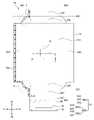
표시 영역(110)은 화상을 표시하는 영역으로 정의된다. 표시 영역(110)은 중앙 표시부(MDA) 및 에지 표시부(SDA)를 포함할 수 있다.The
중앙 표시부(MDA)와 에지 표시부(SDA)는 제1 내지 제4 벤딩 라인(BL1 내지 BL4)에 의해 구분된다. 보다 상세하게는, 중앙 표시부(MDA)는 제1 내지 제4 벤딩 라인(BL1 내지 BL4)에 의해 구획되는 영역의 내측에 위치하며, 구부러지지 않는 영역으로 정의된다. 이에 반해, 에지 표시부(SDA)는 중앙 표시부(MDA)는 제1 내지 제4 벤딩 라인(BL1 내지 BL4)에 의해 구획되는 영역의 외측에 위치하며, 제1 내지 제4 벤딩 라인(BL1 내지 BL4)을 따라, 구부러지는 영역으로 정의된다.The center display unit MDA and the edge display unit SDA are divided by first to fourth bending lines BL1 to BL4. More specifically, the center display unit MDA is located inside the region partitioned by the first to fourth bending lines BL1 to BL4 and is defined as an unbent region. On the other hand, in the edge display unit SDA, the center display unit MDA is located outside the region partitioned by the first to fourth bending lines BL1 to BL4, and the first to fourth bending lines BL1 to BL4 Along , it is defined as a bending region.
중앙 표시부(MDA)는 제1 내지 제3 표시부(DA1 내지 DA3)로 구획될 수 있다. 제1 표시부(DA1)를 기준으로, 제2 표시부(DA2)는 제1 표시부(DA1)로부터 제2 방향(d2)을 따라 인접하게 배치되며, 제3 표시부(DA3)는 제1 표시부(DA1)로부터 제4 방향(d4)을 따라 인접하게 배치된다. 제1 표시부(DA1)의 형상은 일 실시예로, 직사각형일 수 있다. 제2 표시부(DA2) 및 제3 표시부(DA3)의 형상은 일 실시예로, 모서리 영역(A)이 둥근 형태의 직사각형일 수 있다. 즉, 제2 표시부(DA2) 및 제3 표시부(DA3)는 모서리 영역(A)이 라운드 형상일 수 있다. 제2 표시부(DA2) 및 제3 표시부(DA3)의 모서리 영역(A)은 일 실시예로 레이저를 이용하여 기판(100)의 적어도 일부를 컷팅(cutting)함으로써 형성될 수 있다.The central display unit MDA may be divided into first to third display units DA1 to DA3. Based on the first display unit DA1, the second display unit DA2 is disposed adjacent to the first display unit DA1 along the second direction d2, and the third display unit DA3 is disposed adjacent to the first display unit DA1. are disposed adjacent to each other along the fourth direction d4. The shape of the first display unit DA1 may be, in one embodiment, a rectangle. The shape of the second display unit DA2 and the third display unit DA3 may be a rectangle in which the corner area A is rounded in one embodiment. That is, the corner area A of the second display unit DA2 and the third display unit DA3 may have a round shape. The corner area A of the second display unit DA2 and the third display unit DA3 may be formed by cutting at least a portion of the
다만, 상기 직사각형 형상 및 라운드 형상은 도 1에 도시된 것으로 제한되는 것은 아니며, 공정 조건 등을 고려하여 직사각형에 가까운 형상 또는 라운드에 가까운 형상을 모두 포함할 수 있다.However, the rectangular shape and the round shape are not limited to those shown in FIG. 1 , and may include both a shape close to a rectangle or a shape close to a round in consideration of process conditions and the like.
다음으로, 에지 표시부(SDA)에 대해 상세히 설명하기로 한다.Next, the edge display unit SDA will be described in detail.
에지 표시부(SDA)는 도 1을 기준으로 중앙 표시부(MDA)의 좌측 및 우측에 위치하는 제1 에지 표시부(SDA1) 및 중앙 표시부(MDA)의 상측 및 하측에 위치하는 제2 에지 표시부(SDA2)를 포함할 수 있다.The edge display unit SDA includes a first edge display unit SDA1 located on the left and right sides of the center display unit MDA and a second edge display unit SDA2 located above and below the center display unit MDA with reference to FIG. 1 . can include
제1 에지 표시부(SDA1)는 제4 표시부(DA4) 및 제5 표시부(DA5)를 포함할 수 있다. 제4 표시부(DA4)는 제1 표시부(DA1)로부터 제1 방향(d1)을 따라 인접하게 배치된다. 이는, 제4 표시부(DA4)가 제1 표시부(DA1)로부터 제1 방향(d1)을 따라 연장되도록 배치되는 것으로도 표현될 수 있다. 제5 표시부(DA5)는 제1 표시부(DA1)로부터 제3 방향(d3)을 따라 인접하게 배치된다.The first edge display unit SDA1 may include a fourth display unit DA4 and a fifth display unit DA5. The fourth display unit DA4 is disposed adjacent to the first display unit DA1 along the first direction d1. This may also be expressed as the fact that the fourth display unit DA4 is disposed to extend from the first display unit DA1 along the first direction d1. The fifth display unit DA5 is disposed adjacent to the first display unit DA1 along the third direction d3.
제2 에지 표시부(SDA2)는 제6 표시부(DA6) 및 제7 표시부(DA7)를 포함할 수 있다. 제6 표시부(DA6)는 제1 표시부(DA1)로부터 제2 방향(d2)을 따라 인접하게 배치되며, 제7 표시부(DA7)는 제1 표시부(DA1)로부터 제4 방향(d4)을 따라 인접하게 배치된다.The second edge display unit SDA2 may include a sixth display unit DA6 and a seventh display unit DA7. The sixth display unit DA6 is disposed adjacent to the first display unit DA1 along the second direction d2, and the seventh display unit DA7 is adjacent to the first display unit DA1 along the fourth direction d4. are placed so that
제4 내지 제7 표시부(DA4 내지 DA7)의 형상은 일 실시예로 직사각형 형상일 수 있다. 일 실시예로, 제4 표시부(DA4)는 제1 표시부(DA1)를 기준으로 제5 표시부(DA5)와 대칭될 수 있다. 또한, 일 실시예로, 제6 표시부(DA6)는 제1 표시부(DA1)를 기준으로 제7 표시부(DA7)와 대칭될 수 있다. 다만, 제4 내지 제7 표시부(DA4 내지 DA7)의 형상은 도 1에 도시된 것으로 제한되는 것은 아니며, 제4 내지 제7 표시부(DA4 내지 DA7)의 형상은 서로 상이할 수도 있다.The fourth to seventh display units DA4 to DA7 may have a rectangular shape in one embodiment. In an embodiment, the fourth display unit DA4 may be symmetrical to the fifth display unit DA5 based on the first display unit DA1. Also, according to an embodiment, the sixth display unit DA6 may be symmetrical to the seventh display unit DA7 based on the first display unit DA1. However, the shapes of the fourth to seventh display units DA4 to DA7 are not limited to those shown in FIG. 1 , and the shapes of the fourth to seventh display units DA4 to DA7 may be different from each other.
제4 표시부(DA4)는 제1 밴딩 라인(BL1)을 따라 제1 표시부(DA1)의 배면 방향으로 구부러질 수 있다. 제5 표시부(DA5)는 제3 밴딩 라인(BL3)을 따라 제1 표시부(DA1)의 배면 방향으로 구부러질 수 있다. 또한, 제6 표시부(DA6)는 제2 밴딩 라인(BL2)을 따라, 제7 표시부(DA7)는 제4 밴딩 라인(BL4)을 따라 각각 제1 표시부(DA1)의 배면 방향으로 구부러질 수 있다.The fourth display unit DA4 may be bent toward the rear surface of the first display unit DA1 along the first bending line BL1. The fifth display unit DA5 may be bent toward the rear surface of the first display unit DA1 along the third bending line BL3. In addition, the sixth display unit DA6 may be bent along the second bending line BL2, and the seventh display unit DA7 may be bent along the fourth bending line BL4 in the rear direction of the first display unit DA1. .
도 2 및 도 3을 참조하여, 제4 내지 제7 표시부(DA4 내지 DA7)가 구부러진 형태에 대해 보다 상세히 설명하기로 한다.Referring to FIGS. 2 and 3 , the bent shapes of the fourth to seventh display units DA4 to DA7 will be described in more detail.
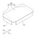
도 2a는 본 발명의 일 실시예에 따른 유기 발광 표시 장치에서 제4 내지 제7 표시부가 구부러진 형태의 표시 영역을 나타낸 정면도이다. 도 2b는 본 발명의 일 실시예에 따른 유기 발광 표시 장치에서 제4 내지 제7 표시부가 구부러진 형태의 표시 영역을 나타낸 측면도이다. 도 3은 본 발명의 일 실시예에 따른 유기 발광 표시 장치를 나타낸 사시도이다.2A is a front view illustrating a curved display area of fourth to seventh displays in an organic light emitting diode display according to an exemplary embodiment of the present invention. 2B is a side view illustrating a display area in which fourth to seventh displays are bent in an organic light emitting diode display according to an exemplary embodiment of the present invention. 3 is a perspective view illustrating an organic light emitting display device according to an exemplary embodiment of the present invention.
도 1, 도 2a 및 도 2b를 참조하면, 본 발명의 일 실시예에 따른 유기 발광 표시 장치(10)는 정면에서 중앙 표시부(MDA), 즉 제1 내지 제3 표시부(DA1 내지 DA3)만 사용자에 의해 관측된다. 이에 따라, 제1 내지 제3 표시부(DA1 내지 DA3)는 사용자에게 정면 방향으로의 영상을 제공한다. 제1 및 제2 에지 표시부(SDA1, SDA2), 즉 제4 내지 제7 표시부(DA4 내지 DA7)는 제1 내지 제4 밴딩 라인(BL1 내지 BL4)에 의해 각각 제1 표시부(DA1)의 배면으로 구부러짐에 따라, 정면에서 사용자에 의해 관측되지 않는다.Referring to FIGS. 1, 2A, and 2B, the organic light emitting
도 2a, 도 2b 및 도 3을 참조하면, 제1 내지 제4 밴딩 라인(BL1 내지 BL4)에 의해 각각 제1 표시부(DA1)의 배면으로 구부러진 제4 내지 제7 표시부(DA4 내지 DA7)는 사용자에게 측면 방향에서의 영상을 제공한다. 도 2b 및 도 3에서는 제4 표시부(DA4) 및 제7 표시부(DA7)에서 영상이 제공되는 것을 예로 든다.Referring to FIGS. 2A, 2B, and 3 , the fourth to seventh display units DA4 to DA7 bent toward the rear surface of the first display unit DA1 by the first to fourth bending lines BL1 to BL4, respectively, are provided to the user. to provide images from the lateral direction. In FIGS. 2B and 3 , images are provided on the fourth display unit DA4 and the seventh display unit DA7 as an example.
한편, 제4 내지 제7 표시부(DA4 내지 DA7)가 메인 표시부(MDA)에 대해 수직으로 구부러진 것으로 도시되어 있으나, 이에 제한되는 것은 아니다. 즉, 제4 내지 제7 표시부(DA4 내지 DA7)는 메인 표시부(MDA)에 대해 소정의 곡률을 갖는 라운드 형상을 갖도록 구부러질 수도 있다. 또한, 제4 내지 제7 표시부(DA4 내지 DA7)는 메인 표시부(MDA)의 배면과 중첩되도록 구부러질 수도 있다.Meanwhile, the fourth to seventh display units DA4 to DA7 are illustrated as being bent vertically with respect to the main display unit MDA, but are not limited thereto. That is, the fourth to seventh display units DA4 to DA7 may be bent to have a round shape having a predetermined curvature with respect to the main display unit MDA. Also, the fourth to seventh display units DA4 to DA7 may be bent to overlap the rear surface of the main display unit MDA.
따라서, 본 발명의 일 실시예에 따른 유기 발광 표시 장치(10)는 제1 내지 제7 표시부(DA1 내지 DA7)를 포함함으로써, 정면 및 4개의 측면 모두에서 영상을 표시할 수 있다. 한편, 중앙 표시부(MDA), 제1 에지 표시부(SDA1) 및 제2 에지 표시부(SDA2)는 일 실시예로 서로 독립적으로 구동될 수 있다. 예를 들어, 메인 표시부(MDA)만 영상을 표시하고, 제1 및 제2 에지 표시부(SDA1, SDA2)는 영상을 표시하지 않을 수 있다. 이와 반대로, 제1 및 제2 에지 표시부(SDA1, SDA2) 중 적어도 일부에서만 영상을 표시할 수도 있다.Accordingly, the organic light emitting
다시 도 1을 참조하면, 비표시 영역(120)은 표시 영역(110)의 외측에 배치되며, 화상을 표시하지 않는 영역으로 정의된다. 비표시 영역(120)은 일 실시예로, 표시 영역(110)을 둘러싸도록 배치될 수 있다. 도 1에서는 비표시 영역(120)이 표시 영역(110)을 둘러싸는 것으로 도시하였으나, 이에 제한되는 것은 아니다. 비표시 영역(120)은 다른 실시예로, 표시 영역(110)의 일 측 또는 타 측에만 인접하게 배치되거나, 또는 표시 영역(110)을 기준으로 표시 영역(110)의 일 측 및 양 측에 각각 인접하게 배치될 수도 있다.Referring back to FIG. 1 , the
구동 집적회로(130)는 비표시 영역(120) 상에 배치될 수 있다. 보다 상세하게는, 구동 집적회로(130)는 비표시 영역(120) 중 제7 표시부(DA7)와 후술하는 출력 패드부(140) 사이의 영역에 배치될 수 있다. 구동 집적회로(130)는 일 실시예로 기판(100) 상에 직접 실장될 수 있다. 한편, 도 1에서는 구동 집적회로(130)를 하나로 도시하였으나, 이에 제한되는 것은 아니며 복수의 구동 집적회로가 비표시 영역(120) 상에 배치될 수도 있다.The driving
구동 집적회로(130)는 출력 패드부(140)로부터 제공받은 구동 신호를 기초로, 복수의 데이터 신호를 생성하여 복수의 화소부(PX)로 제공할 수 있다. 이를 위해, 기판(100) 상에는 출력 패드부(140)와 구동 집적회로(130)를 전기적으로 연결시키는 복수의 입력 라인이 배치될 수 있다. 또한, 기판(100) 상에는 중앙 표시부(MDA) 및 에지 표시부(SDA)와 구동 집적회로(130)를 전기적으로 연결시키는 복수의 출력 라인이 배치될 수 있다.The driving
상기 복수의 입력 라인 및 상기 복수의 출력 라인 각각과 구동 집적회로(130) 간의 전기적인 연결방법은 특별히 제한되지 않는다. 구동 집적회로(130)는 일 실시예로, 이방성 도전 필름(anisotropic conductive film, ACF)을 이용하여, 상기 복수의 입력 라인 및 상기 복수의 출력 라인 각각과 전기적으로 연결될 수 있다. 여기서, 이방성 도전 필름은 일 실시예로 접착 수지 및 접착 수지 내에 분산된 복수의 도전 입자를 포함할 수 있다.An electrical connection method between each of the plurality of input lines and the plurality of output lines and the driving
출력 패드부(140)는 일 실시예로 기판(100)의 가장자리를 따라 제1 방향(d1)으로 연장되는 복수의 출력 패드를 포함할 수 있다. 출력 패드부(140)는 인쇄 회로 기판(PCB: Printed Circuit Board, 도면 미도시)과 전기적으로 연결된다. 인쇄 회로 기판은 일 실시예로 연성 인쇄 회로(FPC: Flexible Printed Circuit)일 수 있다. 인쇄 회로 기판이 연성 인쇄 회로인 경우, 연성 인쇄 회로를 제7 표시부(DA7)의 배면을 향해 접음으로써, 표시 영역(110) 외측에 위치하는 데드 스페이스(dead space)의 면적을 최소화할 수 있다.In one embodiment, the
출력 패드부(140)는 상기 인쇄 회로 기판(PCB)으로부터 제공받은 신호를 구동 집적회로(130)에 제공하거나, 또는 제1 내지 제7 표시부(DA1 내지 DA7)에 직접 제공할 수도 있다.The
기판(100) 상에 비표시 영역(120)과 중첩되는 밴딩 영역(Bending Area: BA)이 배치될 수 있다. 밴딩 영역(BA)은 밴딩 영역(BA) 상에 위치하는 가상의 밴딩 라인을 따라 구부러지는 영역으로 정의된다. 밴딩 영역(BA)은 일 실시예로 제7 표시부(DA7)와 구동 집적회로(130) 사이에 배치될 수 있다. 즉, 기판(100)은 밴딩 영역(BA) 상의 가상의 밴딩 라인을 중심으로 휘어질 수 있다. 이를 통해, 표시 영역(110) 외측에 배치되는 데드 스페이스의 면적을 최소화시킬 수 있다. 상기 밴딩 영역(BA)은 생략될 수도 있다A bending area (BA) overlapping the
신호 배선부(150)는 비표시 영역(120) 상에 배치될 수 있다. 일 실시예로, 신호 배선부(150)는 제7 표시부(DA7), 제3 표시부(DA3), 제4 표시부(DA4), 제2 표시부(DA2) 및 제6 표시부(DA6) 각각의 일 측을 따라 연장되도록 배치될 수 있다.The
신호 배선부(150)는 복수의 구동 신호를 생성하여, 생성된 복수의 구동 신호를 제1 내지 제7 표시부(DA1 내지 DA7) 각각에 배치되는 복수의 화소부(PX)에 제공할 수 있다. 여기서, 구동 신호의 종류는 화소부(PX)에 포함되는 트랜지스터 및 유기 발광 소자 간의 배치 형태에 따라 달라질 수 있다. 예를 들어, 구동 신호는 트랜지스터를 턴 온 시킬 수 있는 스캔 신호이거나, 화소부(PX)의 발광을 제어할 수 있는 발광 제어 신호일 수 있다. 또는 구동 신호는 상기 스캔 신호 및 발광 제어 신호를 모두 포함할 수도 있다. 신호 배선부(150)는 일 실시예로, 상기 구동 신호를 생성하기 위한 복수의 트랜지스터를 포함하거나, 또는 별도의 구동 집적회로를 통해 상기 구동 신호를 생성할 수도 있다.The
신호 배선부(150)가 구동 신호의 생성하고 생성된 구동 신호를 제1 내지 제7 표시부(DA1 내지 DA7)에 제공할 수 있는 경우라면, 신호 배선부(150)의 배치 형태는 도 1에 도시된 것으로 제한되는 것은 아니다.If the
전술한 바와 같이, 구동 신호는 화소부(PX)에 포함되는 트랜지스터 및 유기 발광 소자 간의 배치 형태에 따라 달라질 수 있다. 이하, 화소부(PX)에 포함되는 구성 및 이에 따른 구동 신호에 대해 도 4 내지 도 8을 참조하여 설명하기로 한다.As described above, the driving signal may vary according to the arrangement form between the organic light emitting element and the transistor included in the pixel unit PX. Hereinafter, configurations included in the pixel unit PX and corresponding driving signals will be described with reference to FIGS. 4 to 8 .
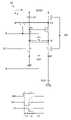
도 4는 도 1에 도시한 화소부의 일 실시예를 나타낸 등가 회로도이다. 도 4에 도시한 화소부는 제j 데이터 라인(DLj, j는 1 이상의 자연수)을 통해 구동 집적회로(130)와 전기적으로 연결되며, 제i 스캔 라인(SLi, i는 1 이상의 자연수)을 통해 신호 배선부(150)와 전기적으로 연결되는 것을 예시한다.FIG. 4 is an equivalent circuit diagram illustrating an embodiment of the pixel unit shown in FIG. 1 . The pixel unit shown in FIG. 4 is electrically connected to the driving
도 4를 참조하면, 화소부(PX)는 스캔 트랜지스터(ST), 구동 트랜지스터(DT), 스토리지 커패시터(Cst) 및 유기 발광 소자(OLED)를 포함할 수 있다.Referring to FIG. 4 , the pixel unit PX may include a scan transistor ST, a driving transistor DT, a storage capacitor Cst, and an organic light emitting diode OLED.
스캔 트랜지스터(ST)는 제3 방향(d3)으로 연장되는 제i 스캔 라인(SLi)과 전기적으로 연결되는 게이트 전극, 제4 방향(d4)으로 연장되는 제j 데이터 라인(DLj)과 전기적으로 연결되는 소스 전극 및 제1 노드(N1)와 전기적으로 연결되는 드레인 전극을 포함할 수 있다. 스캔 트랜지스터(ST)는 제i 스캔 라인(SLi)으로부터 제공받은 제i 스캔 신호(Si)를 기초로 스위칭 동작을 수행하여, 제j 데이터 라인(DLj)으로부터 제공받은 제j 데이터 신호(Dj)를 제1 노드(N1)에 제공할 수 있다.The scan transistor ST has a gate electrode electrically connected to the ith scan line SLi extending in the third direction d3 and electrically connected to the jth data line DLj extending in the fourth direction d4. It may include a source electrode and a drain electrode electrically connected to the first node N1. The scan transistor ST performs a switching operation based on the ith scan signal Si provided from the ith scan line SLi to generate the jth data signal Dj received from the jth data line DLj. It may be provided to the first node N1.
구동 트랜지스터(DT)는 제1 노드(N1)와 전기적으로 연결되는 게이트 전극, 제1 구동 전압(ELVDD)을 제공받는 소스 전극 및 유기 발광 소자(OLED)의 일 전극과 연결되는 드레인 전극을 포함할 수 있다. 유기 발광 소자(OLED)의 타 전극은 제2 구동 전압(ELVSS)이 제공된다. 여기서, 제1 구동 전압(ELVDD) 및 제2 구동 전압(ELVSS)은 직류 전압이며, 제2 구동 전압(ELVSS)은 제1 구동 전압(ELVDD)보다 전압 레벨이 낮다.The driving transistor DT may include a gate electrode electrically connected to the first node N1, a source electrode receiving the first driving voltage ELVDD, and a drain electrode connected to one electrode of the organic light emitting diode OLED. can The second driving voltage ELVSS is provided to the other electrode of the organic light emitting diode OLED. Here, the first driving voltage ELVDD and the second driving voltage ELVSS are DC voltages, and the second driving voltage ELVSS has a lower voltage level than the first driving voltage ELVDD.
이에 따라, 구동 트랜지스터(DT)는 제j 데이터 신호(Dj)를 기초로 스위칭 동작을 수행하여, 유기 발광 소자(OLED)로 흐르는 구동 전류의 전류량을 제어할 수 있다.Accordingly, the driving transistor DT may perform a switching operation based on the jth data signal Dj to control the amount of driving current flowing through the organic light emitting diode OLED.
스토리지 커패시터(Cst)는 제1 노드(N1)와 전기적으로 연결되는 일 전극 및 제1 구동 전압(ELVDD)을 제공받는 타 전극을 포함할 수 있다. 스토리지 커패시터(Cst)는 제1 노드(N1)에 제공되는 전압과 제1 구동 전압(ELVDD) 간의 전압 차를 충전할 수 있다.The storage capacitor Cst may include one electrode electrically connected to the first node N1 and the other electrode receiving the first driving voltage ELVDD. The storage capacitor Cst may charge a voltage difference between the voltage provided to the first node N1 and the first driving voltage ELVDD.
도 4에 도시된 화소부(PX)는 별도의 발광 제어 트랜지스터를 포함하지 않으므로, 전술한 신호 배선부(150)로부터 제1 내지 제7 표시부(DA1 내지 DA7) 각각에 위치하는 복수의 화소부(PX)에 제공되는 구동 신호는 제i 스캔 신호(Si)를 포함하는 복수의 스캔 신호일 수 있다.Since the pixel unit PX shown in FIG. 4 does not include a separate light emission control transistor, a plurality of pixel units ( The driving signal provided to the PX may be a plurality of scan signals including the i th scan signal Si.
다음으로, 도 5를 참조하여, 복수의 화소부(PX)의 다른 실시예에 대해 설명하기로 한다. 도 5에 도시한 화소부의 경우, 도 4에 도시한 화소부(PX)와의 구분을 위해, 도면 부호 PX'를 사용하기로 한다.Next, another embodiment of the plurality of pixel units PX will be described with reference to FIG. 5 . In the case of the pixel unit shown in FIG. 5, reference numeral PX′ will be used to distinguish it from the pixel unit PX shown in FIG. 4.
도 5는 도 1에 도시한 화소부의 다른 실시예를 나타낸 등가 회로도이다. 도 5에 도시한 화소부(PX')는 제j 데이터 라인(DLj)을 통해 구동 집적회로(130)와 전기적으로 연결되며, 서로 이웃하는 제i-1 스캔 라인(SLi-1) 및 제i 스캔 라인(SLi)을 통해 신호 배선부(150)와 전기적으로 연결되는 것을 예시한다. 또한, 화소부(PX')는 신호 배선부(150)와 제i 발광 제어 라인(EMLi)을 통해 전기적으로 연결되는 것을 예시한다.FIG. 5 is an equivalent circuit diagram illustrating another embodiment of the pixel unit shown in FIG. 1 . The pixel unit PX' shown in FIG. 5 is electrically connected to the driving
도 5를 참조하면, 화소부(PX')는 제1 내지 제7 트랜지스터(T1 내지 T7), 스토리지 커패시터(Cst) 및 유기 발광 소자(OLED)를 포함할 수 있다. 제1 내지 제7 트랜지스터(T1 내지 T7)는 일 실시예로 PMOS 트랜지스터일 수 있다. 다만, 이에 제한되는 것은 아니며, 제1 내지 제7 트랜지스터(T1 내지 T7)는 NMOS 트랜지스터일 수도 있다.Referring to FIG. 5 , the pixel unit PX′ may include first to seventh transistors T1 to T7 , a storage capacitor Cst, and an organic light emitting diode OLED. The first to seventh transistors T1 to T7 may be PMOS transistors in one embodiment. However, it is not limited thereto, and the first to seventh transistors T1 to T7 may be NMOS transistors.
제1 트랜지스터(T1)는 제1 노드(N1)와 연결되는 게이트 전극, 제3 노드(N3)와 연결되는 소스 전극 및 제2 노드(N2)와 연결되는 드레인 전극을 포함할 수 있다. 제2 트랜지스터(T2)는 제i 스캔 신호(Si)를 제공받는 게이트 전극, 제j 데이터 라인(DLj)과 연결되는 소스 전극 및 제3 노드(N3)와 연결되는 드레인 전극을 포함할 수 있다.The first transistor T1 may include a gate electrode connected to the first node N1, a source electrode connected to the third node N3, and a drain electrode connected to the second node N2. The second transistor T2 may include a gate electrode receiving the ith scan signal Si, a source electrode connected to the jth data line DLj, and a drain electrode connected to the third node N3.
제2 트랜지스터(T2)는 제i 스캔 신호(Si)를 기초로 스위칭 동작을 수행하여, 제j 데이터 신호(Dj)를 제3 노드(N3)와 연결되는 제1 트랜지스터(T1)의 소스 전극에 제공할 수 있다. 제1 트랜지스터(T1)는 제j 데이터 신호(Dj)를 기초로, 유기 발광 다이오드(OLED)에 제공되는 구동 전류(I1)의 전류량을 제어할 수 있다.The second transistor T2 performs a switching operation based on the i th scan signal Si, and transmits the j th data signal Dj to the source electrode of the first transistor T1 connected to the third node N3. can provide The first transistor T1 may control the amount of driving current I1 provided to the organic light emitting diode OLED based on the jth data signal Dj.
보다 상세하게 설명하기로 한다. 제1 트랜지스터(T1)는 게이트 전극 및 소스 전극 간 전위 차(Vgs, 이하 게이트-소스 전압(Vgs))에 따라, 유기 발광 소자(OLED)에 제공되는 구동 전류(I1)를 제어할 수 있다. 보다 상세하게는, 제1 트랜지스터(T1)는 게이트-소스 전압(Vgs)이 문턱 전압(Vth)보다 클 때 턴 온 되며, 제1 트랜지스터(T1)의 소스 전극의 전압 레벨이 유기 발광 소자(OLED)의 문턱 전압보다 커지면, 제1 트랜지스터(T1)의 소스 전극 및 드레인 전극 간의 전류, 즉 구동 전류(I1)가 유기 발광 소자(OLED)에 제공된다. 즉, 제1 트랜지스터(T1)는 구동 트랜지스터일 수 있으며, 도 4의 구동 트랜지스터(DA)에 대응될 수 있다. 또한, 제2 트랜지스터(T2)는 스캔 트랜지스터일 수 있으며, 도 4의 스캔 트랜지스터(ST)에 대응될 수 있다.It will be described in more detail. The first transistor T1 may control the driving current I1 provided to the organic light emitting diode OLED according to a potential difference between the gate electrode and the source electrode (Vgs, hereinafter referred to as gate-source voltage (Vgs)). More specifically, the first transistor T1 is turned on when the gate-source voltage Vgs is greater than the threshold voltage Vth, and the voltage level of the source electrode of the first transistor T1 is the organic light emitting diode (OLED). ), the current between the source and drain electrodes of the first transistor T1, that is, the driving current I1 is provided to the organic light emitting diode OLED. That is, the first transistor T1 may be a driving transistor and may correspond to the driving transistor DA of FIG. 4 . Also, the second transistor T2 may be a scan transistor and may correspond to the scan transistor ST of FIG. 4 .
제3 트랜지스터(T3)는 제i 스캔 신호(Si)를 제공받는 게이트 전극과, 제1 트랜지스터(T1)의 드레인 전극과 연결되는 소스 전극 및 제1 트랜지스터(T1)의 게이트 전극과 연결되는 드레인 전극을 포함할 수 있다. 제3 트랜지스터(T3)는 제i 스캔 신호(Si)를 기초로 스위칭 동작을 수행하여, 제1 트랜지스터(T1)의 소스 전극 및 게이트 전극을 서로 연결시킬 수 있다. 제3 트랜지스터(T3)는 스위칭 동작을 통해, 제1 트랜지스터(T1)를 다이오드 연결시킴으로써, 제1 트랜지스터(T1)의 문턱 전압(Vth)을 보상할 수 있다. 즉, 제3 트랜지스터(T3)는 보상 트랜지스터일 수 있다.The third transistor T3 includes a gate electrode receiving the i-th scan signal Si, a source electrode connected to the drain electrode of the first transistor T1, and a drain electrode connected to the gate electrode of the first transistor T1. can include The third transistor T3 may perform a switching operation based on the i th scan signal Si to connect the source electrode and gate electrode of the first transistor T1 to each other. The third transistor T3 may compensate for the threshold voltage Vth of the first transistor T1 by diode-connecting the first transistor T1 through a switching operation. That is, the third transistor T3 may be a compensation transistor.
제1 트랜지스터(T1)가 다이오드 연결되면, 제1 트랜지스터(T1)의 소스 전극에 제공되는 제j 데이터 신호(Dj)에 대응되는 전압에서, 제1 트랜지스터(T1)의 문턱 전압(Vth)만큼 하강된 전압이, 제1 트랜지스터(T1)의 게이트 전극에 제공될 수 있다. 상기 제j 데이터 신호(Dj)에 대응되는 전압(Vk)에서, 제1 트랜지스터(T1)의 문턱 전압(Vth)만큼 하강된 전압을 문턱 전압(Vth)이 반영된 전압(Vk-Vth)으로 지칭한다.When the first transistor T1 is diode-connected, the voltage corresponding to the jth data signal Dj provided to the source electrode of the first transistor T1 drops by the threshold voltage Vth of the first transistor T1. The voltage may be applied to the gate electrode of the first transistor T1. A voltage lowered by the threshold voltage Vth of the first transistor T1 from the voltage Vk corresponding to the jth data signal Dj is referred to as a voltage Vk-Vth in which the threshold voltage Vth is reflected. .
제1 트랜지스터(T1)의 게이트 전극은 스토리지 커패시터(Cst)의 일 전극과 연결되어 있으므로, 문턱 전압(Vth)이 반영된 전압(Vk-Vth)은 스토리지 커패시터(Cst)에 의해 유지된다. 제1 트랜지스터(T1)의 문턱 전압(Vth)이 반영된 전압(Vk-Vth)이 게이트 전극에 인가되어 유지되므로, 제1 트랜지스터(T1)에 흐르는 구동 전류(I1)는 제1 트랜지스터(T1)의 문턱 전압(Vth)에 따른 영향을 받지 않는다. 이에 따라, 제1 트랜지스터(T1)의 문턱 전압(Vth) 편차가 보상될 수 있으며, 휘도가 불균일하게 되는 것을 방지할 수 있다.Since the gate electrode of the first transistor T1 is connected to one electrode of the storage capacitor Cst, the voltage Vk-Vth reflecting the threshold voltage Vth is maintained by the storage capacitor Cst. Since the voltage (Vk-Vth) reflecting the threshold voltage (Vth) of the first transistor T1 is applied to the gate electrode and maintained, the driving current I1 flowing through the first transistor T1 is It is not affected by the threshold voltage (Vth). Accordingly, the deviation of the threshold voltage (Vth) of the first transistor T1 may be compensated, and uneven luminance may be prevented.
제4 트랜지스터(T4)는 제i-1 스캔 신호(Si-1)를 제공받는 게이트 전극과, 초기화 전압(VINT)을 제공받는 소스 전극 및 제1 노드(N1)와 연결되는 드레인 전극을 포함할 수 있다. 제4 트랜지스터(T4)는 제i-1 스캔 신호(Si-1)를 기초로 스위칭 동작을 수행하여, 초기화 전압(VINT)을 제1 노드(N1)에 제공할 수 있다. 전술한 바와 같이, 제1 노드(N1)는 제1 트랜지스터(T1)의 게이트 전극과 연결된다. 또한, 제i-1 스캔 신호(Si-1)는 제i 스캔 신호(Si)에 비해 상대적으로 먼저 제공되는 신호이다.The fourth transistor T4 may include a gate electrode receiving the i−1 th scan signal Si−1, a source electrode receiving the initialization voltage VINT, and a drain electrode connected to the first node N1. can The fourth transistor T4 may perform a switching operation based on the i−1 th scan signal Si−1 to provide the initialization voltage VINT to the first node N1. As described above, the first node N1 is connected to the gate electrode of the first transistor T1. Also, the i−1 th scan signal Si−1 is provided relatively earlier than the i th scan signal Si.
따라서, 제4 트랜지스터(T4)는 제2 트랜지스터(T2)가 턴 온 되기 전에 먼저 턴 온 됨으로써, 초기화 전압(VINT)을 제1 트랜지스터(T1)의 게이트 전극에 제공할 수 있다. 초기화 전압(VINT)의 전압 레벨은 제1 트랜지스터(T1)의 게이트 전극의 전압 레벨을 충분히 낮출 수 있는 경우라면, 특별히 제한되지 않는다. 즉, 제4 트랜지스터(T4)는 초기화 트랜지스터일 수 있다.Accordingly, the fourth transistor T4 is turned on before the second transistor T2 is turned on, so that the initialization voltage VINT can be applied to the gate electrode of the first transistor T1. The voltage level of the initialization voltage VINT is not particularly limited as long as the voltage level of the gate electrode of the first transistor T1 can be sufficiently lowered. That is, the fourth transistor T4 may be an initialization transistor.
제5 트랜지스터(T5)는 제i 발광 제어 신호(EMi)를 제공받는 게이트 전극, 제1 구동 전압(ELVDD)을 제공받는 소스 전극 및 제3 노드(N3)와 연결되는 드레인 전극을 포함할 수 있다. 제5 트랜지스터(T5)는 제i 발광 제어 신호(EMi)를 기초로 스위칭 동작을 수행하여, 제1 구동 전압(ELVDD)을 제3 노드(N3)와 연결되는 제1 트랜지스터(T1)의 소스 전극에 제공할 수 있다.The fifth transistor T5 may include a gate electrode receiving the i-th emission control signal EMi, a source electrode receiving the first driving voltage ELVDD, and a drain electrode connected to the third node N3. . The fifth transistor T5 performs a switching operation based on the i-th emission control signal EMi to transfer the first driving voltage ELVDD to the source electrode of the first transistor T1 connected to the third node N3. can be provided to
제6 트랜지스터(T6)는 제i 발광 제어 신호(EMi)를 제공받는 게이트 전극, 제2 노드(N2)와 연결되는 소스 전극 및 제4 노드(N4)와 연결되는 드레인 전극을 포함할 수 있다. 제6 트랜지스터(T6)는 제i 발광 제어 신호(EMi)를 기초로 스위칭 동작을 수행하여, 유기 발광 소자(OLED) 방향으로 구동 전류(I1)가 흐를 수 있도록 전류 경로를 형성할 수 있다. 유기 발광 소자(OLED)는 상기 구동 전류(I1)에 대응하는 발광 전류(I2)에 따라 발광할 수 있다. 즉, 제5 트랜지스터(T5) 및 제6 트랜지스터(T6)는 발광 제어 트랜지스터일 수 있다.The sixth transistor T6 may include a gate electrode receiving the ith emission control signal EMi, a source electrode connected to the second node N2, and a drain electrode connected to the fourth node N4. The sixth transistor T6 may perform a switching operation based on the ith emission control signal EMi to form a current path so that the driving current I1 may flow in the direction of the organic light emitting diode OLED. The organic light emitting diode OLED may emit light according to the emission current I2 corresponding to the driving current I1. That is, the fifth transistor T5 and the sixth transistor T6 may be emission control transistors.
제7 트랜지스터(T7)는 제i 스캔 신호(Si)를 제공받는 게이트 전극, 초기화 전압(VINT)을 제공받는 소스 전극 및 제4 노드(N4)와 연결되는 드레인 전극을 포함할 수 있다. 제7 트랜지스터(T7)가 턴 오프된 상태에서, 초기화 전압(VINT)의 설정 전압에 의해, 제4 노드(N4)에서 제7 트랜지스터(T7) 방향으로 바이패스 전류(I3)가 흐를 수 있다.The seventh transistor T7 may include a gate electrode receiving the i-th scan signal Si, a source electrode receiving the initialization voltage VINT, and a drain electrode connected to the fourth node N4. In a state in which the seventh transistor T7 is turned off, the bypass current I3 may flow from the fourth node N4 toward the seventh transistor T7 by the set voltage of the initialization voltage VINT.
만약, 블랙 영상을 표시하기 위한 제1 트랜지스터(T1)의 최소 전류가 구동 전류(I1)로써 흐를 경우에도, 유기 발광 소자(OLED)가 발광하게 된다면 블랙 영상이 제대로 표시되지 않는다. 즉, 제7 트랜지스터(T7)는 제1 트랜지스터(T1)의 최소 전류의 일부를 바이패스 전류(I3)로써, 유기 발광 소자(OLED) 방향 외의 전류 경로로 분산시킬 수 있다. 여기서, 제1 트랜지스터(T1)의 최소 전류는 제1 트랜지스터(T1)의 게이트-소스 전압(Vgs)이 제1 트랜지스터(T1)의 문턱 전압(Vth)보다 전압 레벨이 낮아, 제1 트랜지스터(T1)가 턴 오프되는 조건에서의 전류를 의미한다. 상기 블랙 영상은 제1 트랜지스터(T1)를 턴 오프시키는 조건에서의 최소 구동 전류가 유기 발광 소자(OLED)에 전달됨으로써 표시된다. 블랙 영상을 표시하는 최소 구동 전류가 흐르는 경우, 바이패스 전류(I3)의 우회 전달의 영향이 크다. 이에 반해, 일반 영상 또는 화이트 영상을 표시하는 구동 전류가 흐르는 경우, 바이패스 전류(I3)의 영향이 거의 없다고 할 수 있다. 이에 따라, 블랙 영상을 표시하는 구동 전류가 흐를 경우, 구동 전류(I1)로부터 제7 트랜지스터(T7)를 통해 빠져나온 바이패스 전류(I3)의 전류량만큼 감소된 유기 발광 소자(OLED)의 발광 전류(I2)는 상기 블랙 영상을 확실히 표현할 수 있을 수준으로의 최소 전류량을 가지게 된다. 따라서, 정확한 블랙 영상을 구현함으로써, 콘트라스트비를 향상시킬 수 있다. 즉, 제7 트랜지스터(T7)는 바이패스 트랜지스터일 수 있다. 한편, 제7 트랜지스터(T7)는 도 2에 도시된 것과 달리, 제i 스캔 신호(Si) 대신 제i-1 스캔 신호(Si-1)를 기초로 스위칭 동작을 수행할 수도 있다.Even when the minimum current of the first transistor T1 for displaying a black image flows as the driving current I1, if the organic light emitting diode OLED emits light, the black image is not properly displayed. That is, the seventh transistor T7 may distribute a portion of the minimum current of the first transistor T1 as the bypass current I3 to a current path other than the organic light emitting diode OLED. Here, the minimum current of the first transistor T1 is determined by the voltage level of the gate-source voltage Vgs of the first transistor T1 being lower than the threshold voltage Vth of the first transistor T1 . ) means the current under the condition that it is turned off. The black image is displayed when the minimum driving current under the condition of turning off the first transistor T1 is transferred to the organic light emitting diode OLED. When the minimum driving current for displaying a black image flows, bypass transfer of the bypass current I3 has a large effect. In contrast, when a driving current for displaying a normal image or a white image flows, it can be said that the bypass current I3 has little effect. Accordingly, when the driving current for displaying a black image flows, the emission current of the organic light emitting diode OLED is reduced by the current amount of the bypass current I3 drained from the driving current I1 through the seventh transistor T7. (I2) has the minimum amount of current at a level that can reliably represent the black image. Accordingly, the contrast ratio may be improved by implementing an accurate black image. That is, the seventh transistor T7 may be a bypass transistor. Meanwhile, the seventh transistor T7 may perform a switching operation based on the i−1 th scan signal Si−1 instead of the i th scan signal Si, unlike that shown in FIG. 2 .
상기 도 5에 도시한 화소부(PX')의 동작에 대해 도 6 내지 도 8을 참조하여 보다 상세히 설명하기로 한다.The operation of the pixel unit PX′ shown in FIG. 5 will be described in detail with reference to FIGS. 6 to 8 .
도 6 내지 도 8은 도 5에 도시한 화소부의 동작을 설명하기 위한 도면이다.6 to 8 are views for explaining the operation of the pixel unit shown in FIG. 5 .
도 6을 참조하면, 제1 구동 구간(P1)동안, 제i-1 스캔 신호(Si-1)는 하이 레벨에서 로우 레벨로 전환된다. 제i 스캔 신호(Si) 및 제i 발광 제어 신호(EMi)는 하이 레벨을 유지한다.Referring to FIG. 6 , during the first driving period P1 , the i−1 th scan signal Si−1 is converted from a high level to a low level. The ith scan signal Si and the ith emission control signal EMi are maintained at a high level.
제i-1 스캔 신호(Si-1)가 하이 레벨에서 로우 레벨로 전환되면, 화소부(PX')의 제4 트랜지스터(T4)가 턴 온 된다. 화소부(PX')의 제4 트랜지스터(T4)는 초기화 전압(VINT)을 제1 노드(N1)에 제공할 수 있다. 여기서, 초기화 전압(VINT)의 레벨은 제1 노드(N1)를 초기화시킬 수 있을 정도로 충분히 낮게 설정될 수 있다. 화소부(PX')의 제4 트랜지스터(T4)의 게이트 전극은 상기 제1 노드(N1)와 전기적으로 연결되므로, 초기화 전압(VINT)으로 설정된다.When the i−1 th scan signal Si−1 is converted from a high level to a low level, the fourth transistor T4 of the pixel unit PX′ is turned on. The fourth transistor T4 of the pixel unit PX′ may provide the initialization voltage VINT to the first node N1. Here, the level of the initialization voltage VINT may be set low enough to initialize the first node N1. Since the gate electrode of the fourth transistor T4 of the pixel unit PX' is electrically connected to the first node N1, the initialization voltage VINT is set.
도 7을 참조하면, 제2 구동 구간(P2) 동안, 제i 스캔 신호(Si)는 하이 레벨에서 로우 레벨로 전환된다. 또한, 제i-1 스캔 신호(Si-1)는 로우 레벨에서 하이 레벨로 전환된다. 제i 발광 제어 신호(EMi)는 하이 레벨을 유지한다.Referring to FIG. 7 , during the second driving period P2 , the i th scan signal Si is converted from a high level to a low level. Also, the i−1 th scan signal Si−1 is converted from a low level to a high level. The ith emission control signal EMi maintains a high level.
이에 따라, 화소부(PX')의 제2 트랜지스터(T2), 제3 트랜지스터(T3) 및 제7 트랜지스터(T7)가 턴 온 되며, 제4 트랜지스터(T4)가 턴 오프 된다. 화소부(PX')의 제3 트랜지스터(T3)가 턴 온 되면, 제1 트랜지스터(T1)는 다이오드(diode) 연결된다. 화소부(PX')의 제2 트랜지스터(T2)를 통해 제j 데이터 라인(DLj)으로부터 제공되는 제1 데이터 신호(D1)는 제3 노드(N3) 및 제3 트랜지스터(T3)를 경유하여, 제1 노드(N1)로 제공된다. 화소부(PX')의 제1 트랜지스터(T1)는 다이오드 연결 상태이므로, 제1 노드(N1)는 제1 데이터 신호(D1)에 대응되는 전압 및 제1 트랜지스터(T1)의 문턱 전압(Vth)의 차전압이 전달된다. 즉, 화소부(PX')의 제1 노드(N1)는 제1 데이터 신호(D1)에 대응되는 전압 레벨에서 화소부(PX')의 제1 트랜지스터(T1)의 문턱 전압(Vth)의 절대값만큼 감소한 차전압이 제공된다.Accordingly, the second transistor T2, the third transistor T3, and the seventh transistor T7 of the pixel unit PX' are turned on, and the fourth transistor T4 is turned off. When the third transistor T3 of the pixel unit PX′ is turned on, the first transistor T1 is diode-connected. The first data signal D1 provided from the j th data line DLj through the second transistor T2 of the pixel unit PX′ passes through the third node N3 and the third transistor T3, It is provided to the first node N1. Since the first transistor T1 of the pixel unit PX′ is in a diode-connected state, the first node N1 has a voltage corresponding to the first data signal D1 and a threshold voltage Vth of the first transistor T1. The differential voltage of is transmitted. That is, the first node N1 of the pixel unit PX' has an absolute threshold voltage Vth of the first transistor T1 of the pixel unit PX' at a voltage level corresponding to the first data signal D1. A differential voltage reduced by the value is provided.
화소부(PX')의 스토리지 커패시터(Cst)는 제1 노드(N1)에 제공된 상기 차전압과 제1 구동 전압(ELVDD) 사이의 전압 차에 대응하는 전하를 저장한다. 한편, 화소부(PX')의 제7 트랜지스터(T7)가 턴 온 되면, 제4 노드(N4)는 초기화 전압(VINT)으로 설정된다.The storage capacitor Cst of the pixel unit PX′ stores charge corresponding to a voltage difference between the difference voltage provided to the first node N1 and the first driving voltage ELVDD. Meanwhile, when the seventh transistor T7 of the pixel unit PX' is turned on, the fourth node N4 is set to the initialization voltage VINT.
도 8을 참조하여, 제3 구동 구간(P3)에 대해 설명하기로 한다. 제3 구동 구간(P3)은 발광 구간으로 정의된다. 제3 구동 구간(P3) 동안, 제i-1 스캔 신호(Si-1)는 하이 레벨을 유지한다. 제i 스캔 신호(Si)는 로우 레벨에서 하이 레벨로 전환된다. 제i 스캔 신호(Si)가 로우 레벨에서 하이 레벨로 전환된 이후, 제i 발광 제어 신호(EMi)는 하이 레벨에서 로우 레벨로 전환된다.Referring to FIG. 8 , the third driving period P3 will be described. The third driving period P3 is defined as an emission period. During the third driving period P3, the i−1 th scan signal Si−1 maintains a high level. The i-th scan signal Si is converted from a low level to a high level. After the ith scan signal Si is converted from the low level to the high level, the ith emission control signal EMi is converted from the high level to the low level.
이에 따라, 제5 트랜지스터(T5) 및 제6 트랜지스터(T6)가 턴 온 되며, 제2 트랜지스터(T2), 제3 트랜지스터(T3) 및 제7 트랜지스터(T7)가 턴 오프 된다. 제5 트랜지스터(T5) 및 제6 트랜지스터(T6)가 턴 온 되면, 제1 구동 전압(ELVDD)으로부터 제5 트랜지스터(T5), 제1 트랜지스터(T1), 제6 트랜지스터(T6)를 경유하여, 유기 발광 다이오드(OLED)에 구동 전류가 흐르게 된다.Accordingly, the fifth transistor T5 and the sixth transistor T6 are turned on, and the second transistor T2, the third transistor T3 and the seventh transistor T7 are turned off. When the fifth transistor T5 and the sixth transistor T6 are turned on, the first drive voltage ELVDD passes through the fifth transistor T5, the first transistor T1, and the sixth transistor T6, A driving current flows through the organic light emitting diode (OLED).
도 5에 도시된 화소부(PX')는 스캔 트랜지스터에 대응되는 제2 트랜지스터(T2), 발광 제어 트랜지스터에 대응되는 제5 및 제6 트랜지스터(T5, T6)을 포함한다. 이에 따라, 전술한 신호 배선부(150)로부터 제1 내지 제7 표시부(DA1 내지 DA7) 각각에 위치하는 복수의 화소부(PX')에 제공되는 구동 신호는 제i 스캔 신호(Si)를 포함하는 복수의 스캔 신호와, 제i 발광 제어 신호(EMi)를 포함하는 복수의 발광 제어 신호일 수 있다.The pixel unit PX′ shown in FIG. 5 includes a second transistor T2 corresponding to the scan transistor and fifth and sixth transistors T5 and T6 corresponding to the emission control transistor. Accordingly, the driving signal provided to the plurality of pixel units PX′ located in each of the first to seventh display units DA1 to DA7 from the aforementioned
한편, 도 4 및 도 5에 도시한 화소부(PX, PX')는 각각 제1 구동 전압(ELVDD) 및 제2 구동 전압(ELVSS)을 제공받을 수 있다. 상기 제1 구동 전압(ELVDD) 및 제2 구동 전압(ELVSS)은 별도의 구동 전압 라인을 통해 전원 제공부(도면 미도시)로부터 제공받을 수 있다. 여기서, 신호 배선부(150)는 상기 구동 전압 라인을 포함할 수도 있다. 또는, 상기 구동 전압 라인은 상기 신호 배선부(150)와 인접하게 배치될 수도 있다.Meanwhile, the pixel units PX and PX′ shown in FIGS. 4 and 5 may receive a first driving voltage ELVDD and a second driving voltage ELVSS, respectively. The first driving voltage ELVDD and the second driving voltage ELVSS may be provided from a power supply unit (not shown) through a separate driving voltage line. Here, the
다음으로, 본 발명의 일 실시예에 따른 유기 발광 표시 장치(10)에 포함되는 구성들의 적층 구조를, 도 5에 도시한 화소부(PX')의 경우를 기준으로 예를 들어 설명하기로 한다.Next, a stacked structure of components included in the organic light emitting
도 9는 도 1에 도시한 I-I'선을 따라 자른 단면도이다. 도 1 내지 도 8에서 설명한 내용과 중복되는 설명은 생략하기로 한다.9 is a cross-sectional view taken along the line II' shown in FIG. 1; Descriptions overlapping those described in FIGS. 1 to 8 will be omitted.
도 9를 참조하면, 버퍼층(210)은 기판(100) 상에 배치될 수 있다. 버퍼층(210)은 기판(100) 상에 배치될 수 있다. 버퍼층(210)은 기판(100)을 통한 외부로부터의 수분 및 산소의 침투를 방지할 수 있다. 또한, 버퍼층(210)은 기판(100)의 표면을 평탄화할 수 있다. 버퍼층(210)은 일 실시예로 질화 규소(SiNx)막, 산화 규소(SiO2)막 및 산질화규소(SiOxNy)막 중 어느 하나를 포함할 수 있다. 버퍼층(210)은 기판(100)의 종류 또는 공정 조건 등에 따라 생략될 수도 있다.Referring to FIG. 9 , a
반도체 패턴(ACT)을 포함하는 반도체층은 버퍼층(210) 상에 배치될 수 있다. 반도체층에 대해 반도체 패턴(ACT)을 기준으로 설명하기로 한다. 반도체 패턴(ACT)은 일 실시예로, 다결정 실리콘, 단결정 실리콘, 저온 다결정 실리콘, 비정질 실리콘 및 산화물 반도체 중에서 선택되는 하나 또는 두 개 이상을 혼합하여 형성될 수 있다. 반도체 패턴(ACT)은 일 실시예로 불순물이 도핑되지 않은 채널 영역(ACTa), 불순물이 도핑된 소스 영역(ACTb) 및 드레인 영역(ACTc)을 포함할 수 있다. 소스 영역(ACTb)은 채널 영역(ACTa)의 일 측에 위치하며, 후술하는 소스 전극(SE)과 전기적으로 연결된다. 드레인 영역(ACTc)은 채널 영역(ACTa)의 타 측에 위치하며, 후술하는 드레인 전극(DE)과 전기적으로 연결된다.A semiconductor layer including the semiconductor pattern ACT may be disposed on the
제1 절연층(220)은 반도체 패턴(ACT)을 포함하는 반도체층 상에 배치될 수 있다. 제1 절연층(220)은 일 실시예로 게이트 절연층일 수 있다. 제1 절연층(220)은 일 실시예로 실리콘 산화물(SiOx), 실리콘 질화물(SiNx) 등의 무기 절연물질, BCB(BenzoCycloButene), 아크릴계 물질, 및 폴리이미드와 같은 유기 절연 물질로 이루어진 군에서 선택된 어느 하나 또는 하나 이상의 물질을 혼합하여 형성할 수 있다.The first insulating
게이트 전극(GE)을 포함하는 게이트 도전체는 제1 절연층(220) 상에 배치될 수 있다. 여기서, 게이트 전극(GE)은 도 5에 도시한 제1 트랜지스터(T1)의 게이트 전극이다. 게이트 도전체는 도 5에 도시한 제i 스캔 라인(SLi)도 포함할 수 있다. 게이트 전극(GE)은 제i 스캔 라인(SLi)으로부터 연장될 수 있으며, 반도체 패턴(ACT)과 중첩될 수 있다. 게이트 도전체는 예컨대, 알루미늄 합금을 포함하는 알루미늄(Al) 계열의 금속, 은 합금을 포함하는 은(Ag) 계열의 금속, 구리 합금을 포함하는 구리(Cu)계열의 금속, 몰리브덴 합금을 포함하는 몰리브덴(Mo) 계열 금속, 크롬(Cr), 티탄(Ti), 및 탄탈륨(Ta) 중 어느 하나 이상을 포함할 수 있다.A gate conductor including the gate electrode GE may be disposed on the first insulating
제2 절연층(230)은 게이트 전극(GE)을 포함하는 게이트 도전체 상에 배치될 수 있다. 제2 절연층(230)은 실리콘 산화물(SiOx), 실리콘 질화물(SiNx) 등의 무기 절연물질, BCB(BenzoCycloButene), 아크릴계 물질, 및 폴리이미드와 같은 유기 절연 물질로 이루어진 군에서 선택된 어느 하나 또는 하나 이상의 물질을 혼합하여 형성할 수 있다.The second
소스 전극(SE) 및 드레인 전극(DE)을 포함하는 데이터 도전체는 제2 절연층(230) 상에 배치될 수 있다. 여기서, 소스 전극(SE)은 도 5에 도시한 제1 트랜지스터(T1)의 소스 전극이다. 또한, 드레인 전극(DE)은 도 5에 도시한 제1 트랜지스터(T1)의 드레인 전극이다.A data conductor including the source electrode SE and the drain electrode DE may be disposed on the second insulating
데이터 도전체는 도 2에 도시한 제j 데이터 라인(DLj)뿐만 아니라, 도 5에 도시한 제1 구동 전압(ELVDD) 및 제2 구동 전압(ELVSS)을 제공하는 구동 전압 라인을 포함할 수 있다. 소스 전극(SE) 및 드레인 전극(DE)은 제2 절연층(230) 상에 서로 이격되어 배치된다. 데이터 도전체는 금속, 합금, 금속 질화물, 도전성 금속 산화물, 투명 도전성 물질으로 이루어진 군 중 선택된 하나 이상을 포함할 수 있다. 데이터 도전체는 일 실시예로 니켈(Ni), 코발트(Co), 티탄(Ti), 은(Ag), 구리(Cu), 몰리브덴(Mo), 알루미늄(Al), 베릴륨(Be), 니오브(Nb), 금(Au), 철(Fe), 셀렌(Se) 또는 탄탈륨(Ta) 등으로 이루어진 단일막 또는 다중막 구조를 가질 수 있다. 또한, 상기 금속에 티탄(Ti), 지르코늄(Zr), 텅스텐(W), 탄탈륨(Ta), 니오브(Nb), 백금(Pt), 하프늄(Hf), 산소(O) 및 질소(N)로 이루어진 군에서 선택된 하나 이상의 원소를 포함시켜 형성한 합금이 소스 전극(SE) 및 드레인 전극(DE)의 재료로서 이용될 수 있다.The data conductor may include not only the jth data line DLj shown in FIG. 2 , but also the driving voltage lines shown in FIG. 5 providing the first driving voltage ELVDD and the second driving voltage ELVSS. . The source electrode SE and the drain electrode DE are spaced apart from each other on the second insulating
전술한, 반도체 패턴(ACT), 게이트 전극(GE), 소스 전극(SE) 및 드레인 전극(DE)은 도 5의 제1 트랜지스터(T1)를 구성한다.The aforementioned semiconductor pattern ACT, gate electrode GE, source electrode SE, and drain electrode DE constitute the first transistor T1 of FIG. 5 .
평탄화층(240)은 데이터 도전체 상에 배치될 수 있다. 평탄화층(240)은 단차를 제거함에 따라, 후술하는 화소 전극(250) 및 유기 발광층(270)의 발광 효율을 높일 수 있다. 평탄화층(240)은 일 실시예로 유기 물질을 포함할 수 있다. 예를 들어, 평탄화층(240)은 폴리이미드(polyimide), 폴리아크릴(polyacryl) 및 폴리실록산(polysiloxane) 중 선택된 어느 하나 이상을 포함하여 이루어질 수 있다. 다른 실시예로, 평탄화층(240)은 무기 물질을 포함하여 구성되거나, 또는 무기 물질 및 유기 물질의 복합 형태로 구성될 수도 있다. 평탄화층(240)에는 드레인 전극(DE)의 적어도 일부를 노출시키는 제1 컨택홀(CNT1)이 형성될 수 있다.The
화소 전극(250)은 평탄화층(240) 상에 배치될 수 있다. 화소 전극(250)은 제1 컨택홀(CNT1)에 의해 노출된 드레인 전극(DE)과 전기적으로 연결될 수 있다. 즉, 화소 전극(250)은 정공 주입 전극인 애노드(anode)일 수 있다. 화소 전극(250)이 애노드 전극인 경우, 화소 전극(250)은 정공 주입이 용이하도록 일함수가 높은 물질을 포함할 수 있다. 또한, 화소 전극(250)은 반사형 전극, 반투과형 전극 또는 투과형 전극일 수 있다. 화소 전극(250)은 일 실시예로 반사성 재료를 포함할 수 있다. 반사성 재료는 일 실시예로, 은(Ag), 마그네슘(Mg), 크롬(Cr), 금(Au), 백금(Pt), 니켈(Ni), 구리(Cu), 텅스텐(W), 알루미늄(Al), 알루미늄-리튬(Al-Li), 마그네슘-인듐(Mg-In) 및 마그네슘-은(Mg-Ag)으로 이루어진 군에서 선택된 하나 이상을 포함할 수 있다.The
화소 전극(250)은 일 실시예로, 단일막으로 형성될 수 있으나, 이에 한정되는 것은 아니다. 즉, 화소 전극(250)은 2 이상의 물질이 적층된 다중막으로 형성될 수도 있다.The
화소 전극(250)이 다중막으로 형성되는 경우, 화소 전극(250)은 일 실시예로, 반사막 및 상기 반사막 상에 배치되는 투명 또는 반투명 전극을 포함할 수 있다. 다른 실시예로, 화소 전극(250)은 반사막 및 상기 반사막 하부에 배치되는 투명 또는 반투명 전극을 포함할 수 있다. 예를 들면, 화소 전극(250)은 ITO/Ag/ITO의 3층 구조를 가질 수 있으나, 이에 한정되는 것은 아니다.When the
여기서, 투명 또는 반투명 전극은 ITO(Indium Tin Oxide), IZO(Indium Zinc Oxide), ZnO(Zinc Oxide), In2O3(Indiu, Oxide), (IGO, Indium Gallium Oxide) 및 AZO(Aluminum Zinc Oxide)로 이루어진 군에서 선택된 하나 이상을 포함하여 이루어질 수 있다.Here, the transparent or translucent electrode is made of ITO (Indium Tin Oxide), IZO (Indium Zinc Oxide), ZnO (Zinc Oxide), In2O3 (Indiu, Oxide), (IGO, Indium Gallium Oxide) and AZO (Aluminum Zinc Oxide). It may consist of one or more selected from the group.
화소 정의막(260)은 화소 전극(250) 상에 배치될 수 있다. 화소 정의막(260)은 화소 전극(250)의 적어도 일부를 노출하는 개구부를 포함한다. 화소 정의막(260)은 유기 물질 또는 무기 물질을 포함할 수 있다. 일 실시예로, 화소 정의막(260)은 포토 레지스트, 폴리이미드계 수지, 아크릴계 수지, 실리콘 화합물, 폴리아크릴계 수지 등의 재료를 포함할 수 있다.The
유기 발광층(270)은 화소 전극(250) 및 화소 정의막(260) 상에 배치될 수 있다. 보다 상세하게는, 유기 발광층(270)은 화소 전극(250) 중 화소 정의막(260)의 개구부를 통해 노출되는 영역 상에 배치될 수 있다. 유기 발광층(270)은 일 실시예로, 화소 정의막(260)의 측벽의 적어도 일부를 덮을 수 있다.The
유기 발광층(270)은 일 실시예로 적색, 청색 및 녹색 중 하나의 색을 발광할 수 있다. 다른 실시예로, 유기 발광층(270)은 백색을 발광하거나, 또는 시안(cyan), 마젠타(magenta) 및 옐로우(yellow) 중 하나의 색을 발광할 수도 있다. 유기 발광층(270)이 백색을 발광하는 경우, 유기 발광층(270)은 백색 발광 재료를 포함하거나, 또는 적색 발광층, 녹색 발광층 및 청색 발광층이 적층된 형태를 가짐으로써 백색을 발광할 수도 있다.The organic
공통 전극(280)은 유기 발광층(270) 및 화소 정의막(260) 상에 배치될 수 있다. 공통 전극(280)은 일 실시예로 유기 발광층(270) 및 화소 정의막(260) 상에 전면적으로 형성될 수 있다. 공통 전극(280)은 일 실시예로 캐소드(cathode) 전극일 수 있다. 공통 전극(280)은 일 실시예로 Li. Ca, Lif/Ca, LiF/Al, Al, Ag, Mg로 이루어진 군에서 선택된 어느 하나 이상을 포함할 수 있다. 또한, 공통 전극(280)은 일함수가 낮은 재료로 이루어질 수 있다. 공통 전극(280)은 일 실시예로 ITO(Indium Tin Oxide), IZO(Indium Zinc Oxide), ZnO(Zinc Oxide), In2O3(Indiu, Oxide), (IGO, Indium Gallium Oxide) 및 AZO(Aluminum Zinc Oxide)로 이루어진 군에서 선택된 어느 하나 이상을 포함하는 투명 또는 반투명 전극일 수 있다.The
전술한, 화소 전극(250), 유기 발광층(270) 및 공통 전극(280)은 유기 발광 소자(OLED)를 구성할 수 있다. 다만, 이에 제한되는 것은 아니며, 유기 발광 소자(OLED)는 정공 주입층(HIL), 정공 수송층(HTL), 전자 수송층(ETL) 및 전자 주입층(EIL) 등을 더 포함하는 다층 구조일 수 있다.The
봉지층(300)은 기판(100)과 대향되도록 배치되되, 유기 발광 소자(OLED)를 덮을 수 있다. 봉지층(300)은 외부로부터 유입될 수 있는 수분 및 공기 등이 유기 발광 소자(OLED)에 침투하는 것을 방지할 수 있다. 봉지층(300)은 일 실시예로 제1 무기층(301), 유기층(302) 및 제2 무기층(303)을 포함할 수 있다.The
제1 무기층(301)은 공통 전극(280) 상에 배치될 수 있다. 제1 무기층(301)은 실리콘 옥사이드(SiOx), 실리콘 나이트라이드(SiNx), 실리콘 옥시나이트라이드(SiONx)로 이루어진 군에서 선택된 어느 하나 이상을 포함하여 이루어질 수 있다.The first
유기층(302)은 제1 무기층(301) 상에 배치될 수 있다. 유기층(302)은 에폭시, 아크릴레이트 또는 우레탄아크릴레이트로 이루어진 군에서 선택된 어느 하나를 포함하여 이루어질 수 있다. 유기층(302)은 화소 정의막(260)에 의한 단차를 평탄화시킬 수 있다.The
제2 무기층(303)은 유기층(302) 상에 배치될 수 있다. 제2 무기층(303)은 실리콘 옥사이드(SiOx), 실리콘 나이트라이드(SiNx), 실리콘 옥시나이트라이드(SiONx)로 이루어진 군에서 선택된 어느 하나 이상을 포함하여 이루어질 수 있다.The second
한편, 도 9에서는 제1 무기층(301), 유기층(302) 및 제2 무기층(303)이 각각 단일 층인 것으로 도시하였으나, 이에 제한되는 것은 아니다. 즉, 제1 무기층(301), 유기층(302) 및 제2 무기층(303) 중 적어도 하나의 층은 다층 구조로 형성될 수도 있다.Meanwhile, in FIG. 9 , each of the first
봉지층(300)은 다른 실시예로 HMDSO층(Hexamethyldisiloxane layer)을 포함할 수 있다. 보다 상세하게는, 봉지층(300)은 제1 무기층(301), 제2 무기층(303) 및 상기 제1 무기층(301)과 제2 무기층(303) 사이에 배치되는 HMDSO층을 포함할 수 있다. 즉, 전술한 유기층(302)이 HMDSO층으로 대체될 수 있다.In another embodiment, the
상기 HMDSO층은 일 실시예로 제1 무기층(301) 형성 이후, 동일한 챔버(chamber)를 통해 형성될 수 있다. 이를 통해, 봉지층(300) 형성 공정을 간소화할 수 있다. 또한, 스트레스(stress)를 흡수할 수 있는 HMDSO층을 포함함으로써, 봉지층(300)은 충분한 유연성을 가질 수 있다.In one embodiment, the HMDSO layer may be formed through the same chamber after the formation of the first
이와는 달리, 봉지층(300)은 투명 절연 기판일 수도 있다. 여기서, 투명 절연 기판은 유리 기판, 석영 기판, 투명 수지 기판 등일 수 있다. 봉지층(300)이 투명 절연 기판인 경우, 봉지층(300)은 기판(100)과 별도의 실링(sealing) 부재를 통해 결합될 수 있다.Alternatively, the
도면에는 도시하지 않았으나, 봉지층(300) 상에는 편광층, 입력 감지층 및 윈도우 층이 배치될 수 있다.Although not shown in the drawings, a polarization layer, an input sensing layer, and a window layer may be disposed on the
편광층은 외부로부터 입사되는 외부 광의 반사율을 저감시킬 수 있다. 일 실시예로 편광층은 위상 지연자(retarder) 및 편광자(polarizer)를 포함할 수 있다. 편광층은 생략될 수도 있다. 편광층이 생략되는 경우, 봉지층(300) 상에는 외광 반사에 의한 색 분리를 개선하기 위해, 블랙 매트릭스(Black matrix) 및 컬러 필터(Color filter)가 배치될 수 있다.The polarization layer may reduce reflectance of external light incident from the outside. In one embodiment, the polarization layer may include a phase retarder and a polarizer. The polarization layer may be omitted. When the polarization layer is omitted, a black matrix and a color filter may be disposed on the
입력 감지층은 일 실시예로 봉지층(300) 상에 직접 형성될 수 있다. 다른 실시예로, 입력 감지층은 별도의 접착 부재를 통해 봉지층(300)과 결합될 수도 있다.The input sensing layer may be directly formed on the
다음으로, 본 발명의 일 실시예에 따른 유기 발광 표시 장치(10)의 구동 신호 특성 및 이를 보상하는 방법에 대해 설명하기로 한다.Next, driving signal characteristics of the organic light emitting
먼저, 도 10a 및 도 10b을 참조하여, 신호 배선부(150)로부터 출력되는 구동 신호의 특성에 대해 설명하기로 한다.First, with reference to FIGS. 10A and 10B , characteristics of a driving signal output from the
도 10a는 본 발명의 일 실시예에 따른 유기 발광 표시 장치의 구동 신호 특성을 설명하기 위한 도면이다. 도 10b는 도 10a에 도시한 B 영역을 확대한 도면이다. 이하, 도 10a에 도시한 B 영역을 기준으로 설명하되, 보다 상세하게는, 제1a, 제1b, 제2a, 제2b, 제3a 및 제3b 화소부, 상기 제1a, 제1b, 제2a, 제2b, 제3a 및 제3b 화소부 각각과 전기적으로 연결되는 제1 내지 제3 스캔 라인(SL1 내지 SL3) 및 제1 내지 제3 발광 제어 라인(EML1 내지 EML3)을 기준으로 설명하기로 한다. 여기서, 화소부를 지칭하는 “제1a 내지 제3b”와, 스캔 라인 및 발광 제어 라인을 지칭하는 “제1 내지 제3”은 서로 간의 구분을 위한 것이며, 배치 순서 등을 한정하는 것은 아니다. 한편, 제1a 내지 제3b 화소부(PX1a 내지 PX3b)는 도 5에 도시한 화소부(PX')의 구성을 포함하는 것으로 예시한다.10A is a diagram for explaining driving signal characteristics of an organic light emitting diode display according to an exemplary embodiment of the present invention. FIG. 10B is an enlarged view of region B shown in FIG. 10A. Hereinafter, a description will be made based on region B shown in FIG. 10A, but in more detail, first 1a, 1b, 2a, 2b, 3a and 3b pixel units, the 1a, 1b, 2a, The first to third scan lines SL1 to SL3 and the first to third emission control lines EML1 to EML3 electrically connected to the 2b, 3a, and 3b pixel units will be described as references. Here, "first to third" referring to the pixel unit and "first to third" referring to the scan line and the emission control line are for distinction between each other, and do not limit the arrangement order. Meanwhile, it is exemplified that the 1a to 3b pixel units PX1a to PX3b include the configuration of the pixel unit PX′ shown in FIG. 5 .
도 10a 및 도 10b를 참조하면, 제1 스캔 라인(SL1)은 신호 배선부(150)로부터 제3 방향(d3)을 따라 연장될 수 있다. 제1 스캔 라인(SL1)은 제4 표시부(DA4), 제1 표시부(DA1) 및 제5 표시부(DA5)와 중첩되도록 배치될 수 있다. 제1 스캔 라인(SL1)은 제4 표시부(DA4), 제1 표시부(DA1) 및 제5 표시부(DA5) 각각에 배치되는 복수의 화소부들과 전기적으로 연결될 수 있다. 즉, 제1 스캔 라인(SL1)은 제1 밴딩 라인(BL1) 및 제3 밴딩 라인(BL3)을 따라 각각 구부러지는 제4 표시부(DA4) 및 제5 표시부(DA5)와 중첩됨에 따라, 적어도 두 개의 구부러지는 영역(E1 및 E2)을 포함할 수 있다.Referring to FIGS. 10A and 10B , the first scan line SL1 may extend from the
제2 스캔 라인(SL2)은 신호 배선부(150)로부터 제3 방향(d3)을 따라 연장되되, 제2 표시부(DA2)와 중첩되도록 배치될 수 있다. 제3 스캔 라인(SL3)은 신호 배선부(150)로부터 제3 방향(d3)을 따라 연장되되, 제6 표시부(DA6)와 중첩되도록 배치될 수 있다.The second scan line SL2 extends from the
제1 스캔 라인(SL1)이 제4 표시부(DA4), 제1 표시부(DA1) 및 제5 표시부(DA5) 모두와 중첩되므로, 제1 스캔 라인(SL1)의 길이(l1)는 제2 스캔 라인(SL2)의 길이(l2) 및 제3 스캔 라인(SL3)의 길이(l3)보다 길다. 한편, 제2 표시부(DA2)의 폭은 제6 표시부(DA6)의 폭보다 넓을 수 있다. 이에 따라, 제2 표시부(DA2)와 중첩되는 제2 스캔 라인(SL2)의 길이(l2)는 제6 표시부(DA6)와 중첩되는 제3 스캔 라인(SL3)의 길이(l3)보다 길 수 있다.Since the first scan line SL1 overlaps all of the fourth display unit DA4, the first display unit DA1, and the fifth display unit DA5, the length l1 of the first scan line SL1 is equal to the length l1 of the second scan line SL1. It is longer than the length l2 of SL2 and the length l3 of the third scan line SL3. Meanwhile, the width of the second display unit DA2 may be wider than that of the sixth display unit DA6. Accordingly, the length l2 of the second scan line SL2 overlapping the second display unit DA2 may be longer than the length l3 of the third scan line SL3 overlapping the sixth display unit DA6. .
즉, 제1 내지 제3 스캔 라인(SL1 내지 SL3)의 길이가 서로 다르므로, 이에 따라 스캔 라인으로부터 출력되는 스캔 신호 간의 슬루 레잇(slew rate)가 상이해질 수 있다.That is, since the lengths of the first to third scan lines SL1 to SL3 are different from each other, slew rates between scan signals output from the scan lines may be different accordingly.
예를 들어 설명하기로 한다. 제1a 화소부(PX1a)는 제1 스캔 라인(SL1)과 연결되되, 제1 스캔 라인(SL1)과 연결된 화소부 중 가장 먼저 턴 온 전압을 갖는 제1 스캔 신호(S1)를 제공받는 화소부를 예시한다. 제1b 화소부(PX1b)는 제1 스캔 라인(SL1)과 연결되되, 제1 스캔 라인(SL1)과 연결된 화소부 중 가장 나중에 턴 온 전압을 갖는 제1 스캔 신호(S1)를 제공받는 화소부를 예시한다.Let me explain with an example. The 1a pixel unit PX1a is connected to the first scan line SL1, and the pixel unit receives the first scan signal S1 having the turn-on voltage first among the pixel units connected to the first scan line SL1. foreshadow The 1b pixel unit PX1b is connected to the first scan line SL1 and includes a pixel unit that receives the first scan signal S1 having the last turn-on voltage among the pixel units connected to the first scan line SL1. foreshadow
제1b 화소부(PX1b)는 제1a 화소부(PX1a)에 비해, 상대적으로 나중에 턴 온 전압을 갖는 제1 스캔 신호(S1)가 제공되므로, 제1 스캔 라인(SL1) 자체의 배선 저항 성분으로 인한 전압 강하(IR drop)로 인해, 제1a 화소부(PX1a)에 제공되는 제1 스캔 신호(S1)와 제1b 화소부(PX1b)에 제공되는 제1 스캔 신호(S1) 간의 슬루 레잇이 상이하게 될 수 있다. 이에 따라, 제1b 화소부(PX1b)는 연결된 데이터 라인으로부터 데이터 신호를 충분히 제공받을 수 있는 시간을 확보하지 못하게 된다. 여기서, 상기 시간은 결국 화소부에 포함되어 상기 스캔 신호를 제공받는 트랜지스터가 턴 온 되기 위한 전압 레벨을 제공하는 시간을 의미하며, 이하 상기 시간을 턴 온 타임(turn on time)으로 정의한다. 제1b 화소부(PX1b), 보다 상세하게는 제2 트랜지스터(T2, 도 5 참조)의 턴 온 타임을 충분히 확보하지 못하는 경우, 필요로 하는 데이터 신호를 충분히 제공받지 못하게 되어, 화질 불량을 야기시키게 된다.Since the first scan signal S1 having a turn-on voltage is provided to the 1b pixel unit PX1b relatively later than the 1a pixel unit PX1a, the wiring resistance component of the first scan line SL1 itself The slew rate between the first scan signal S1 provided to the 1a pixel unit PX1a and the first scan signal S1 provided to the 1b pixel unit PX1b is different due to the voltage drop (IR drop) caused by the can be done Accordingly, the 1b pixel unit PX1b cannot secure enough time to receive a data signal from the connected data line. Here, the time means a time for providing a voltage level for turning on a transistor included in a pixel unit and receiving the scan signal. Hereinafter, the time is defined as a turn on time. If the turn-on time of the 1b pixel unit PX1b, more specifically, the second transistor T2 (see FIG. 5) is not sufficiently secured, required data signals cannot be sufficiently provided, resulting in poor image quality. do.
전술한 슬루 레잇 차이는 제2 스캔 라인(SL2)과 연결되는 제2a 화소부(PX2a) 및 제2b 화소부(PX2b) 간에서도 발생될 수 있다. 또한, 제3 스캔 라인(SL3)과 연결되는 제3a 화소부(PX3a) 및 제3b 화소부(PX3b) 간에서도 발생될 수 있다.The aforementioned slew rate difference may also occur between the 2a pixel unit PX2a and the 2b pixel unit PX2b connected to the second scan line SL2 . In addition, it may also occur between the 3a pixel unit PX3a and the 3b pixel unit PX3b connected to the third scan line SL3.
한편, 상기 슬루 레잇 차이는 스캔 라인의 길이에 영향을 받으므로, 서로 길이가 상이한 제1 내지 제3 스캔 라인(SL1 내지 SL3)과 각각 연결되는 제1b 화소부(PX1b), 제2b 화소부(PX2b) 및 제3b 화소부(PX3b) 각각의 슬루 레잇도 서로 상이할 수 있다.Meanwhile, since the slew rate difference is affected by the length of the scan line, the first to third scan lines SL1 to SL3 having different lengths are respectively connected to the 1b pixel unit PX1b and the 2b pixel unit ( Slew rates of each of the PX2b) and the 3b pixel units PX3b may also be different from each other.
제1 발광 제어 라인(EML1)은 신호 배선부(150)로부터 제3 방향(d3)을 따라 연장될 수 있다. 제1 발광 제어 라인(EML1)은 제4 표시부(DA4), 제1 표시부(DA1) 및 제5 표시부(DA5)와 중첩되도록 배치될 수 있다. 제1 발광 제어 라인(EML1)은 제4 표시부(DA4), 제1 표시부(DA1) 및 제5 표시부(DA5) 각각에 배치되는 복수의 화소부들과 전기적으로 연결될 수 있다. 제1 발광 제어 라인(EML1)은 제1 밴딩 라인(BL1) 및 제3 밴딩 라인(BL3)을 따라 각각 구부러지는 제4 표시부(DA4) 및 제5 표시부(DA5)와 중첩됨에 따라, 적어도 두 개의 구부러지는 영역(E1 및 E2)을 포함할 수 있다.The first emission control line EML1 may extend along the third direction d3 from the
제2 발광 제어 라인(EML2)은 신호 배선부(150)로부터 제3 방향(d3)을 따라 연장되되, 제2 표시부(DA2)와 중첩되도록 배치될 수 있다. 제3 발광 제어 라인(EML3)은 신호 배선부(150)로부터 제3 방향(d3)을 따라 연장되되, 제6 표시부(DA6)와 중첩되도록 배치될 수 있다.The second emission control line EML2 extends from the
제1 발광 제어 라인(EML1)으로부터 제1a 및 제1b 화소부(PX1a, PX1b)에 제공되는 제1 발광 제어 신호(EM1), 제2 발광 제어 라인(EML2)으로부터 제2a 및 제2b 화소부(PX2a, PX2b)에 제공되는 제2 발광 제어 신호(EM2) 및 제3 발광 제어 라인(EML3)으로부터 제3a 및 제3b 화소부(PX3a, PX3b)에 제공되는 제3 발광 제어 신호(EM3) 간에도 각 발광 제어 라인의 길이(l4, l5, l6) 및 화소부의 배치 위치 차이로 인해, 슬루 레잇이 상이할 수 있다.The first emission control signal EM1 provided from the first emission control line EML1 to the 1a and 1b pixel units PX1a and PX1b, and the 2a and 2b pixel units from the second emission control line EML2 ( Also between the second emission control signal EM2 provided to PX2a and PX2b and the third emission control signal EM3 provided to the 3a and 3b pixel units PX3a and PX3b from the third emission control line EML3. Slew rates may be different due to differences in the lengths of the emission control lines (14, 15, and 16) and the arrangement positions of the pixel units.
이하, 상기 슬루 레잇 차이를 보상하기 위한 방법에 대해 도 11 내지 도 14를 참조하여 설명하기로 한다.Hereinafter, a method for compensating for the slew rate difference will be described with reference to FIGS. 11 to 14 .
도 11 내지 도 14는 본 발명의 일 실시예에 따른 유기 발광 표시 장치의 슬루 레잇 차이를 보상하기 위한 방법을 설명하기 위한 도면이다.11 to 14 are diagrams for explaining a method for compensating for a slew rate difference of an organic light emitting diode display according to an exemplary embodiment of the present invention.
도 11a를 먼저 참조하면, 신호 배선부(150)는 신호 배선부(150)와 연결되는 스캔 라인의 길이를 고려하여, 스캔 라인으로 제공되는 스캔 신호의 턴 온 타임의 길이를 조절할 수 있다. 보다 상세하게는, 신호 배선부(150)는 상대적으로 길이가 긴 스캔 라인에 제공되는 스캔 신호의 턴 온 타임의 길이를, 길이가 짧은 스캔 라인에 제공되는 스캔 신호의 턴 온 타임의 길이보다, 길도록 조절할 수 있다. Referring first to FIG. 11A , the
예를 들어 설명하기로 한다. 제1 스캔 라인(SL1)에 제공되는 제1 스캔 신호(S1)의 턴 온 타임의 길이(t1)는 제2 스캔 라인(SL2)에 제공되는 제2 스캔 신호(S2)의 턴 온 타임의 길이(t2) 및 제3 스캔 라인(SL3)에 제공되는 제3 스캔 신호(S3)의 턴 온 타임의 길이(t3)보다 길다. 한편, 제2 스캔 신호(S2)의 턴 온 타임의 길이(t2)는 제3 스캔 신호(S3)의 턴 온 타임의 길이(t3)보다 길 수 있다.Let me explain with an example. The turn-on time length t1 of the first scan signal S1 provided to the first scan line SL1 is the length of the turn-on time of the second scan signal S2 provided to the second scan line SL2. (t2) and the length of the turn-on time (t3) of the third scan signal S3 provided to the third scan line SL3. Meanwhile, the turn-on time length t2 of the second scan signal S2 may be longer than the turn-on time length t3 of the third scan signal S3.
상기 제1 스캔 신호(S1)의 턴 온 타임의 길이(t1)가 제2 스캔 신호(S2)의 턴 온 타임의 길이(t2) 및 제3 스캔 신호(S3)의 턴 온 타임의 길이(t3)보다 긴 경우라면, 각 턴 온 타임의 길이의 값은 특별히 제한되지 않는다. 일 실시예로, 각 턴 온 타임의 길이는, 제1 내지 제3 스캔 라인(SL1 내지 SL3)의 길이에 따른 슬루 레잇 차이를 보상함으로써, 각 스캔 라인이 배치되는 표시부 간의 휘도 차이를 최소화시킬 수 있을 정도로 설정될 수 있다.The turn-on time length t1 of the first scan signal S1 is equal to the turn-on time length t2 of the second scan signal S2 and the turn-on time length t3 of the third scan signal S3. ), the value of the length of each turn-on time is not particularly limited. In an embodiment, the length of each turn-on time compensates for the slew rate difference according to the lengths of the first to third scan lines SL1 to SL3, thereby minimizing a luminance difference between display units where each scan line is disposed. It can be set to such an extent that there is.
따라서, 제1 스캔 신호(S1)를 제공받는 제1b 화소부(PX1b)의 경우, 제1 스캔 신호(S1)가 충분한 턴 온 타임을 가짐으로써, 제1b 화소부(PX1b)와 연결된 데이터 라인으로부터 제공받는 데이터 신호에 대응되는 전압을 스토리지 커패시터(Cst, 도 5 참조)에 충전할 수 있는 시간을 충분히 확보할 수 있다. 이를 통해, 각 표시부 간의 휘도 차이를 최소화시킬 수 있어 표시 품질을 향상시킬 수 있으며, 상기 휘도 차이로 인해 표시 영역(110)에 발생될 수 있는 가로줄 시인 현상을 개선할 수 있다.Therefore, in the case of the 1b pixel unit PX1b receiving the first scan signal S1, the first scan signal S1 has a sufficient turn-on time, so that the data line connected to the 1b pixel unit PX1b A sufficient amount of time may be secured to charge the storage capacitor (Cst, see FIG. 5) with a voltage corresponding to the provided data signal. Through this, it is possible to minimize the luminance difference between the respective display units, thereby improving display quality, and improving the visibility of horizontal lines that may occur in the
한편, 도 5를 함께 참조하면, 충분한 시간 동안 제1 내지 제3 발광 제어 신호(EM1 내지 EM3)가 턴 오프되지 않으면, 도 7에서 설명한 제1 트랜지스터(T1)의 문턱 전압(Vth) 보상이 제대로 수행되지 않는다. 한편, 발광 제어 신호를 제공받는 트랜지스터가 턴 오프되기 위한 전압 레벨을 제공하는 시간을 이하 턴 오프 타임(turn off time)으로 정의한다.Meanwhile, referring to FIG. 5 , if the first to third emission control signals EM1 to EM3 are not turned off for a sufficient time, the threshold voltage Vth compensation of the first transistor T1 described in FIG. 7 is not properly performed. not carried out Meanwhile, a time period during which a transistor receiving a light emitting control signal provides a voltage level for turning off is defined as a turn off time.
도 11b를 참조하면, 신호 배선부(150)는 신호 배선부(150)와 연결되는 발광 제어 라인의 길이를 고려하여, 발광 제어 라인으로 제공되는 발광 제어 신호의 턴 오프 타임의 길이를 조절할 수 있다. 보다 상세하게는, 신호 배선부(150)는 상대적으로 길이가 긴 발광 제어 라인에 제공되는 발광 제어 신호의 턴 오프 타임의 길이를, 길이가 짧은 발광 제어 라인에 제공되는 발광 제어 신호의 턴 오프 타임의 길이보다, 길게 할 수 있다.Referring to FIG. 11B , the
예를 들어 설명하기로 한다. 제1 발광 제어 라인(EML1)에 제공되는 제1 발광 제어 신호(EM1)의 턴 오프 타임의 길이(t4)는 제2 발광 제어 라인(EML2)에 제공되는 제2 발광 제어 신호(EM2)의 턴 오프 타임의 길이(t5) 및 제3 발광 제어 라인(EML3)에 제공되는 제3 발광 제어 신호(EM3)의 턴 오프 타임의 길이(t6)보다 길다. 한편, 제2 발광 제어 신호(EM2)의 턴 오프 타임의 길이(t5)는 제3 발광 제어 신호(EM3)의 턴 오프 타임의 길이(t6)보다 길 수 있다.Let me explain with an example. The length t4 of the turn-off time of the first light emission control signal EM1 provided to the first light emission control line EML1 is equal to the turn-off time of the second light emission control signal EM2 provided to the second light emission control line EML2. It is longer than the off-time length t5 and the turn-off time length t6 of the third light emission control signal EM3 provided to the third light emission control line EML3. Meanwhile, the turn-off time length t5 of the second light emission control signal EM2 may be longer than the turn-off time length t6 of the third light emission control signal EM3.
따라서, 제1 발광 제어 신호(EM1)를 제공받는 제1b 화소부(PX1b)의 경우, 제1 발광 제어 신호(EM1)가 충분한 턴 오프 타임을 가짐으로써, 제1 트랜지스터(T1, 도 5 참조)의 문턱 전압(Vth)을 보상할 수 있는 시간을 충분히 확보할 수 있다.Therefore, in the case of the 1b pixel unit PX1b receiving the first emission control signal EM1, the first emission control signal EM1 has a sufficient turn-off time, so that the first transistor T1 (see FIG. 5) It is possible to secure enough time to compensate for the threshold voltage (Vth) of
도 12a를 참조하면, 도 11a에 도시된 것과 달리, 제2 스캔 신호(S2)의 턴 온 타임의 길이(t2)는 제3 스캔 신호(S3)의 턴 온 타임의 길이(t3)와 동일할 수도 있다.Referring to FIG. 12A, unlike the case shown in FIG. 11A, the turn-on time length t2 of the second scan signal S2 may be the same as the turn-on time length t3 of the third scan signal S3. may be
즉, 제2 스캔 라인(SL2)의 길이(l2) 및 제3 스캔 라인(SL3)의 길이(l3)의 차이는 제3 스캔 라인(SL3)의 길이(l3)와 제1 스캔 라인(SL1)의 길이(l1)의 차이에 비해 작다. 이에 따라, 도 11a에 도시된 것과 같이, 제2 스캔 신호(S2)의 턴 온 타임의 길이(t2)는 제3 스캔 신호(S3)의 턴 온 타임의 길이(t3)를 동일하게 형성할 수도 있다.That is, the difference between the length l2 of the second scan line SL2 and the length l3 of the third scan line SL3 is the difference between the length l3 of the third scan line SL3 and the length l3 of the first scan line SL1. is smaller than the difference in length (l1) of Accordingly, as shown in FIG. 11A, the turn-on time length t2 of the second scan signal S2 may be identical to the turn-on time length t3 of the third scan signal S3. there is.
또한, 도 12b를 참조하면, 도 12a에 도시된 것과 달리, 제2 발광 제어 신호(EM2)의 턴 오프 타임의 길이(t5)는 제3 발광 제어 신호(EM3)의 턴 오프 타임의 길이(t6)와 동일할 수도 있다.Also, referring to FIG. 12B, unlike that shown in FIG. 12A, the turn-off time length t5 of the second light emission control signal EM2 is the turn-off time length t6 of the third light emission control signal EM3. ) may be the same as
다만, 각 스캔 신호의 턴 온 타임 및 각 발광 제어 신호의 턴 오프 타임은 도 11 및 도 12에서 설명한 것으로 한정되는 것은 아니며, 각 스캔 신호가 제공되는 스캔 라인 및 각 발광 제어 신호가 제공되는 발광 제어 라인의 길이를 고려하여, 조절될 수 있다.However, the turn-on time of each scan signal and the turn-off time of each light emission control signal are not limited to those described in FIGS. 11 and 12, and the scan line provided with each scan signal and light emission control provided with each light emission control signal. Considering the length of the line, it can be adjusted.
도 13 및 도 14를 참조하여, 각 스캔 라인의 슬루 레잇 차이를 보상하기 위한 다른 실시예에 대해 설명하기로 한다.Referring to FIGS. 13 and 14 , another embodiment for compensating for a slew rate difference of each scan line will be described.
도 13에 도시한 스캔 신호의 경우, 도 12에 도시한 스캔 신호와 비교하여, 턴 온 타임의 길이(t)는 서로 동일하되, 펄스 폭의 길이가 서로 다른 점에서 차이가 있다.In the case of the scan signal shown in FIG. 13, compared to the scan signal shown in FIG. 12, the length (t) of the turn-on time is the same, but the length of the pulse width is different from each other.
신호 배선부(150)는 신호 배선부(150)와 연결되는 스캔 라인의 길이를 고려하여, 스캔 라인으로 제공되는 스캔 신호의 펄스 폭의 길이를 조절할 수 있다. 여기서, 펄스 폭은 스캔 신호의 최저 전압과 최고 전압 간의 전압 레벨 차이로 정의된다. 보다 상세하게는, 신호 배선부(150)는 상대적으로 길이가 긴 스캔 라인에 제공되는 스캔 신호의 펄스 폭의 길이를, 길이가 짧은 스캔 라인에 제공되는 스캔 신호의 펄스 폭의 길이보다, 길도록 조절할 수 있다.The
예를 들어 설명하기로 한다. 제1 스캔 라인(SL1)에 제공되는 제1 스캔 신호(S1)의 펄스 폭의 길이(h1)는 제2 스캔 라인(SL2)에 제공되는 제2 스캔 신호(S2)의 펄스 폭의 길이(h2) 및 제3 스캔 라인(SL3)에 제공되는 제3 스캔 신호(S3)의 펄스 폭의 길이(h3)보다 길다. 한편, 제2 스캔 신호(S2)의 펄스 폭의 길이(h2)는 제3 스캔 신호(S3)의 펄스 폭의 길이(h3)보다 길 수 있다.Let me explain with an example. The length h1 of the pulse width of the first scan signal S1 provided to the first scan line SL1 is equal to the length h2 of the pulse width of the second scan signal S2 provided to the second scan line SL2. ) and the pulse width h3 of the third scan signal S3 provided to the third scan line SL3. Meanwhile, the length h2 of the pulse width of the second scan signal S2 may be longer than the length h3 of the pulse width of the third scan signal S3.
상기 제1 스캔 신호(S1)의 펄스 폭의 길이(h1)가 제2 스캔 신호(S2)의 펄스 폭의 길이(h2) 및 제3 스캔 신호(S3)의 펄스 폭의 길이(h3)보다 긴 경우라면, 각 펄스 폭의 길이 값은 특별히 제한되지 않는다. 일 실시예로, 펄스 폭의 길이는, 제1 내지 제3 스캔 라인(SL1 내지 SL3)의 길이에 따른 슬루 레잇 차이를 보상함으로써, 각 스캔 라인이 배치되는 표시부 간의 휘도 차이를 최소화시킬 수 있을 정도로 설정될 수 있다.The pulse width length h1 of the first scan signal S1 is longer than the pulse width length h2 of the second scan signal S2 and the pulse width length h3 of the third scan signal S3. In this case, the length value of each pulse width is not particularly limited. In an embodiment, the length of the pulse width is set to a level capable of minimizing a luminance difference between display units where each scan line is disposed by compensating for a slew rate difference according to the lengths of the first to third scan lines SL1 to SL3. can be set.
이를 통해, 각 표시부 간의 휘도 차이를 최소화시킬 수 있어 표시 품질을 향상시킬 수 있으며, 상기 휘도 차이로 인해 표시 영역(110)에 발생될 수 있는 가로줄 시인 현상을 개선할 수 있다.Through this, it is possible to minimize the luminance difference between the respective display units, thereby improving display quality, and improving the visibility of horizontal lines that may occur in the
도 14는 참조하면, 도 13에 도시된 것과 달리, 제2 스캔 신호(S2)의 펄스 폭의 길이(h2)는 제3 스캔 신호(S3)의 펄스 폭의 길이(h3)와 동일할 수도 있다.Referring to FIG. 14 , unlike the case shown in FIG. 13 , the length h2 of the pulse width of the second scan signal S2 may be equal to the length h3 of the pulse width of the third scan signal S3. .
즉, 제2 스캔 라인(SL2)의 길이(l2) 및 제3 스캔 라인(SL3)의 길이(l3)의 차이는 제3 스캔 라인(SL3)의 길이(l3)와 제1 스캔 라인(SL1)의 길이(l1)의 차이에 비해 작다. 이에 따라, 도 14에 도시된 것과 같이, 제2 스캔 신호(S2)의 펄스 폭의 길이(h2)는 제3 스캔 신호(S3)의 펄스 폭의 길이(h3)를 동일하게 형성할 수도 있다.That is, the difference between the length l2 of the second scan line SL2 and the length l3 of the third scan line SL3 is the difference between the length l3 of the third scan line SL3 and the length l3 of the first scan line SL1. is smaller than the difference in length (l1) of Accordingly, as shown in FIG. 14 , the length h2 of the pulse width of the second scan signal S2 may be identical to the length h3 of the pulse width of the third scan signal S3.
한편, 본 발명의 일 실시예에 따른 유기 발광 표시 장치는 상기 턴 온 타임의 길이 및 펄스 폭의 길이 모두를 조절함으로써, 슬루 레잇 차이를 보상할 수도 있다.Meanwhile, the organic light emitting diode display according to an exemplary embodiment of the present invention may compensate for the slew rate difference by adjusting both the length of the turn-on time and the length of the pulse width.
다음으로, 본 발명의 일 실시예에 따른 유기 발광 표시 장치(10)의 데이터 신호 특성 및 이를 보상하는 방법에 대해 설명하기로 한다.Next, data signal characteristics of the organic light emitting
도 15는 본 발명의 일 실시예에 따른 유기 발광 표시 장치의 데이터 신호 특성을 설명하기 위한 도면이다. 도 15에서는, 제1 데이터 라인(DL1), 제2 데이터 라인(DL2) 및 제3 데이터 라인(DL3)을 기준으로 설명하기로 한다. 여기서 데이터 라인을 지칭하는 “제1 내지 제3”은 서로 간의 구분을 위한 것이며, 데이터 라인의 배치 순서 등을 한정하는 것은 아니다.15 is a diagram for explaining data signal characteristics of an organic light emitting diode display according to an exemplary embodiment of the present invention. In FIG. 15 , the first data line DL1 , the second data line DL2 , and the third data line DL3 will be described as references. Here, "first to third" referring to the data lines are for distinction between each other, and do not limit the arrangement order of the data lines.
이하, 제1 내지 제3 데이터 라인(DL1 내지 DL3)과 연결되는 제4a 화소부(PX4a), 제4b 화소부(PX4b), 제4c 화소부(PX4c), 제4d 화소부(PX4d) 및 제4e 화소부(PX4e)를 기준으로 설명하기로 한다.Hereinafter, the 4a th pixel unit PX4a, the 4b th pixel unit PX4b, the 4c th pixel unit PX4c, the 4d th pixel unit PX4d, and the th pixel unit PX4a connected to the first to third data lines DL1 to DL3 The description will be made based on the 4e pixel unit PX4e.
여기서, 제4a 화소부(PX4a)는 제1 데이터 라인(DL1)과 연결되되, 제4 표시부(DA4)에 배치된다. 제4b 화소부(PX4b)는 제2 데이터 라인(DL2)과 연결되되, 제1 표시부(DA1)에 배치된다. 제4c 화소부(PX4c)는 제3 데이터 라인(DL3)과 연결되되, 제5 표시부(DA5)에 배치된다. 또한, 제4d 화소부(PX4d) 및 제4e 화소부(PX4e)는 각각 제2 표시부(DA2) 및 제6 표시부(DA6)에 배치되되, 동일한 제2 데이터 라인(DL2)과 연결된다. 한편, 제4a 화소부(PX4a), 제4b 화소부(PX4b) 및 제4c 화소부(PX4c)는 서로 동일한 행에 배치됨에 따라, 동일한 스캔 라인과 연결된다.Here, the 4th pixel unit PX4a is connected to the first data line DL1 and disposed on the fourth display unit DA4. The 4b pixel unit PX4b is connected to the second data line DL2 and disposed on the first display unit DA1. The 4c pixel unit PX4c is connected to the third data line DL3 and disposed on the fifth display unit DA5. In addition, the 4d pixel unit PX4d and the 4e pixel unit PX4e are disposed on the second display unit DA2 and the sixth display unit DA6, respectively, and are connected to the same second data line DL2. Meanwhile, the 4a th pixel unit PX4a , the 4b th pixel unit PX4b , and the 4c th pixel unit PX4c are disposed on the same row and connected to the same scan line.
전술한 바와 같이, 제4 표시부(DA4) 및 제5 표시부(DA5)는 각각 제1 밴딩 라인(BA1) 및 제2 밴딩 라인(BA2)을 따라 제1 표시부(DA1)의 배면 방향으로 구부러진다. 이에 따라, 제4 표시부(DA4)에 배치되는 제4a 화소부(PX4a)에 제1 데이터 신호(D1)를 제공하기 위한 제1 데이터 라인(DL1)은 제1 영역(F1)에 위치하는 구부러진 영역(bent portion)을 가질 수 있다. 또한, 제5 표시부(DA5)에 배치되는 제4c 화소부(PX4a)에 제3 데이터 신호(D3)를 제공하기 위한 제3 데이터 라인(DL3)은 제2 영역(F2)에 위치하는 구부러진 영역을 가질 수 있다. 이에 반해, 제4b 화소부(PX4b)에 제2 데이터 신호(D2)를 제공하기 위한 제2 데이터 라인(DL2)은 구부러진 영역을 포함하지 않는다.As described above, the fourth display unit DA4 and the fifth display unit DA5 are bent toward the rear surface of the first display unit DA1 along the first and second bending lines BA1 and BA2, respectively. Accordingly, the first data line DL1 for providing the first data signal D1 to the 4a pixel unit PX4a disposed on the fourth display unit DA4 is a bent area located in the first area F1. (bent portion). In addition, the third data line DL3 for providing the third data signal D3 to the 4c pixel unit PX4a disposed on the fifth display unit DA5 has a bent area located in the second area F2. can have In contrast, the second data line DL2 for providing the second data signal D2 to the 4b pixel unit PX4b does not include a bent area.
이에 따라, 동일한 행에 배치되는 제4a 화소부(PX4a), 제4b 화소부(PX4b) 및 제4c 화소부(PX4c)와 각각 연결되는 제1 내지 제3 데이터 라인(DL1 내지 DL3)의 길이는 서로 상이할 수 있다. 보다 상세하게는, 구동 집적회로(130)에서부터 제4a 화소부(PX4a), 제4b 화소부(PX4b) 및 제4c 화소부(PX4c) 각각까지의 데이터 라인의 길이는 서로 상이할 수 있다.Accordingly, the lengths of the first to third data lines DL1 to DL3 respectively connected to the 4a th pixel unit PX4a, the 4b th pixel unit PX4b, and the 4c th pixel unit PX4c disposed in the same row are may differ from each other. More specifically, the lengths of the data lines from the driving
상기 데이터 라인의 길이가 상이함에 따라, 데이터 라인의 배선 저항으로 인한 전압 강하로 인해, 각 데이터 라인과 연결되는 화소부 간의 휘도 차이 및 세로줄 시인 현상이 발생될 수 있다.As the lengths of the data lines are different, a voltage drop due to wiring resistance of the data lines may cause a luminance difference and a vertical line visibility phenomenon between pixel units connected to each data line.
또한, 동일한 제2 데이터 라인(DL2)에 연결되는 제4b 화소부(PX4b), 제4d 화소부(PX4d) 및 제4e 화소부(PX4e) 간에도, 상대적으로 구동 집적회로(130)와의 거리 차이가 존재하므로, 이에 따른 제1 내지 제7 표시부(DA1 내지 DA7) 간의 휘도 차이가 발생될 수 있다. 즉, 각 표시부에 동일한 데이터 신호를 인가하더라도, 상대적으로 제1 표시부(DA1)의 휘도가 나머지 표시부에 비해 휘도가 높을 수 있다.Also, there is a relatively large distance difference from the driving
따라서, 본 발명의 일 실시예에 따른 유기 발광 표시 장치(10)는 화소부가 배치되는 표시부의 위치를 고려하여, 보정된 데이터 신호를 상기 화소부에 제공할 수 있다.Accordingly, the organic light emitting
제2 데이터 라인(DL2)을 기준으로 예를 들어 설명하기로 한다.An example will be described based on the second data line DL2.
제2 데이터 라인(DL2)과 연결되는 제4b 화소부(PX4b), 제4d 화소부(PX4d) 및 제4e 화소부(PX4e) 중 제6 표시부(DA6)에 배치되는 제4d 화소부(PX4d)가 제4b 화소부(PX4b) 및 제4e 화소부(PX4e)에 비해 휘도가 상대적으로 낮으므로, 제4d 화소부(PX4d)를 기준으로, 제4b 화소부(PX4b) 및 제4e 화소부(PX4e)에 제공되는 데이터 신호를 보정할 수 있다.A 4d pixel unit PX4d disposed on the sixth display unit DA6 among the 4b th pixel unit PX4b, 4d px4d and 4e px unit PX4e connected to the second data line DL2. Since the luminance is relatively lower than that of the 4b-th pixel unit PX4b and the 4e-th pixel unit PX4e, the 4d-th pixel unit PX4d is the standard, the 4b-th pixel unit PX4b and the 4e-th pixel unit PX4e ) can be corrected for the data signal provided.
보다 상세하게는, 제4d 화소부(PX4d)에 제공되는 제2 데이터 신호(D2)는 그대로 제4d 화소부(PX4d)에 제공하되, 제4e 화소부(PX4e)가 원래 표시해야할 계조 데이터에서 보정을 통해 계조 값을 낮춘 제2 데이터 신호(D2)가 제4e 화소부(PX4e)에 제공될 수 있다. 또한, 제4b 화소부(PX4b)가 원래 표시해야할 계조 데이터에서 보정을 통해 계조 값을 낮춘 제2 데이터 신호(D2)가 제4b 화소부(PX4b)에 제공될 수 있다. 여기서, 제4b 화소부(PX4b)에 제공되는 보정된 제2 데이터 신호(D2)의 계조 값은 제4e 화소부(PX4e)에 제공되는 보정된 제2 데이터 신호(D2)의 계조 값보다 낮을 수 있다.More specifically, the second data signal D2 supplied to the 4d pixel unit PX4d is provided to the 4d pixel unit PX4d as it is, but the grayscale data that the 4e pixel unit PX4e should originally display is corrected. The second data signal D2 having a lowered grayscale value may be provided to the 4e pixel unit PX4e. In addition, the second data signal D2 obtained by lowering the grayscale value through correction in the grayscale data to be originally displayed by the 4b pixel unit PX4b may be provided to the 4b pixel unit PX4b. Here, the gray level value of the corrected second data signal D2 provided to the 4b pixel unit PX4b may be lower than the gray level value of the corrected second data signal D2 provided to the 4e pixel unit PX4e. there is.
상기 계조 값을 낮추는 정도는 구동 집적회로(130)와 당해 화소부 간의 거리를 기초로 결정될 수 있다. 보다 상세하게는, 거리가 가장 가까운 화소부에 제공되는 데이터 신호에 대응되는 계조 데이터의 계조 값을 낮추는 정도가 가장 클 수 있다.The degree of lowering the grayscale value may be determined based on a distance between the driving
즉, 제1 내지 제7 표시부(DA1 내지 DA7)에 배치되는 복수의 화소부(PX)에 제공되는 데이터 신호의 계조 값을, 각 화소부와 구동 집적회로(130) 간의 거리를 고려하여 조절함으로써, 제1 내지 제7 표시부(DA1 내지 DA7)의 휘도 균일성을 향상시킬 수 있다.That is, the grayscale value of the data signal provided to the plurality of pixel units PX disposed on the first to seventh display units DA1 to DA7 is adjusted in consideration of the distance between each pixel unit and the driving
이하, 본 발명의 다른 실시예에 따른 유기 발광 표시 장치에 대해 설명하기로 한다. 다만, 도 1 내지 도 15에서 설명한 내용과 중복되는 설명은 생략하기로 한다.Hereinafter, an organic light emitting display device according to another exemplary embodiment of the present invention will be described. However, descriptions overlapping those described in FIGS. 1 to 15 will be omitted.
도 16 내지 도 19는 본 발명의 다른 실시예에 따른 유기 발광 표시 장치를 개략적으로 나타낸 평면도이다.16 to 19 are plan views schematically illustrating an organic light emitting display device according to another exemplary embodiment of the present invention.
도 16을 먼저 참조하여 설명하기로 한다. 도 16에 도시한 유기 발광 표시 장치(20)는 도 1에 도시한 유기 발광 표시 장치(10)와 비교하여, 제1 신호 배선부(150a) 및 제2 신호 배선부(150b)를 포함하는 점에서 차이가 있다. 즉, 도 16에 도시한 유기 발광 표시 장치(20)는 도 1에 도시한 유기 발광 표시 장치(10)의 신호 배선부(150)에 대응되는 제1 신호 배선부(150a) 뿐만 아니라, 중앙 표시부(MDA)를 기준으로 제1 신호 배선부(150a)에 대응되는 제2 신호 배선부(150b)를 더 포함할 수 있다.It will be described with reference to FIG. 16 first. Compared to the organic light emitting
제2 신호 배선부(150b)는 제7 표시부(DA7), 제3 표시부(DA3), 제4 표시부(DA4), 제2 표시부(DA2) 및 제6 표시부(DA6) 각각의 타 측을 따라 연장되도록 배치될 수 있다.The second
제1 및 제2 신호 배선부(150a, 150b)는 복수의 구동 신호를 생성하여, 생성된 복수의 구동 신호를 제1 내지 제7 표시부(DA1 내지 DA7) 각각에 배치되는 복수의 화소부(PX)에 제공할 수 있다.The first and second
일 실시예로, 제1 신호 배선부(150a) 및 제2 신호 배선부(150b)는 서로 동일한 신호를 생성하여 각각 복수의 화소부(PX)에 제공할 수 있다. 예를 들어, 제1 신호 배선부(150a) 및 제2 신호 배선부(150b) 모두가 제1 스캔 신호(S1)를 제1 스캔 라인(SL1)에 제공하는 경우, 상기 제1 스캔 신호(S1)가 제공되는 제1 스캔 라인(SL1)의 배선 저항에 의한 전압 강하를 방지할 수 있다. 다만, 이 경우에도, 제1 스캔 라인(SL1)의 길이가 제2 스캔 라인(SL2) 및 제3 스캔 라인(SL3) 각각의 길이 차이로 인해 발생되는 슬루 레잇 차이를 보상하기 위해, 제1 스캔 라인(SL1)에 제공되는 제1 스캔 신호(S1)의 턴 온 타임 및/또는 펄스 폭의 길이를 상대적으로 길게 형성할 수 있다.In an embodiment, the first
다른 실시예로, 제1 신호 배선부(150a) 및 제2 신호 배선부(150b)는 서로 다른 신호를 생성하여 각각 복수의 화소부(PX)에 제공할 수도 있다. 예를 들어, 제1 신호 배선부(150a)는 전술한 복수의 스캔 신호를 생성하여, 복수의 화소부(PX)에 제공하는 스캔 구동부일 수 있다. 제2 신호 배선부(150b)는 전술한 복수의 발광 제어 신호를 생성하여, 복수의 화소부(PX)에 제공하는 발광 구동부일 수 있다.In another embodiment, the first
도 17을 참조하면, 제2 표시부(DA2) 및 제3 표시부(DA3)는 모서리 영역(A1)이 직각으로 형성될 수 있다. 즉, 도 17에 도시된 유기 발광 표시 장치(30)는 제2 표시부(DA2) 및 제3 표시부(DA3)의 모서리 영역(A1)이 직각인 점에서, 라운드 형상을 갖는 모서리 영역(A)을 포함하는 도 1에 도시한 유기 발광 표시 장치(10)와 차이가 있다.Referring to FIG. 17 , the corner area A1 of the second display unit DA2 and the third display unit DA3 may be formed at right angles. That is, the organic light emitting
신호 배선부(150)는 제7 표시부(DA7), 제3 표시부(DA3), 제4 표시부(DA4), 제2 표시부(DA2) 및 제6 표시부(DA6)의 외곽을 따라 연장되되, 대체로 인접한 표시부의 외곽 형상과 동일한 형상을 가질 수 있다.The
도 18에 도시한 유기 발광 표시 장치(40)는 제6 표시부(DA6)를 포함하지 않는 점에서, 도 1에 도시한 유기 발광 표시 장치(10)와 차이가 있다.The organic light emitting
또한, 도 19에 도시한 유기 발광 표시 장치(50)는 제5 표시부(DA5)를 추가로 포함하지 않는 점에서, 도 18에 도시한 유기 발광 표시 장치(40)와 차이가 있다.In addition, the organic light emitting
즉, 반드시 제1 내지 제7 표시부(DA1 내지 DA7) 모두를 포함하지 않더라도, 동일 방향으로 연장되는 스캔 라인, 데이터 라인 또는 발광 제어 라인드 간의 길이 차로 인해 휘도 차이가 발생되는 경우, 각 라인에 제공되는 신호의 턴 온 타임의 길이, 펄스 폭의 길이 및/또는 데이터 보상 방법을 조절함으로써, 복수의 표시부의 휘도 차이를 최소화시킬 수 있다.That is, even if the first to seventh display units DA1 to DA7 are not necessarily included, when a difference in luminance occurs due to a difference in length between scan lines, data lines, or emission control lines extending in the same direction, provided to each line. A difference in luminance of a plurality of display units may be minimized by adjusting the length of the turn-on time of the signal, the length of the pulse width, and/or the data compensation method.
이상에서 본 발명의 실시예를 중심으로 설명하였으나 이는 단지 예시일 뿐 본 발명을 한정하는 것이 아니며, 본 발명이 속하는 분야의 통상의 지식을 가진 자라면 본 발명의 실시예의 본질적인 특성을 벗어나지 않는 범위에서 이상에 예시되지 않은 여러 가지의 변형과 응용이 가능함을 알 수 있을 것이다. 예를 들어, 본 발명의 실시예에 구체적으로 나타난 각 구성 요소는 변형하여 실시할 수 있다. 그리고 이러한 변형과 응용에 관계된 차이점들은 첨부된 청구 범위에서 규정하는 본 발명의 범위에 포함되는 것으로 해석되어야 할 것이다.Although the above has been described with reference to the embodiments of the present invention, this is only an example and does not limit the present invention, and those skilled in the art to which the present invention pertains will do without departing from the essential characteristics of the embodiments of the present invention. It will be appreciated that various modifications and applications not exemplified above are possible. For example, each component specifically shown in the embodiment of the present invention can be modified and implemented. And differences related to these modifications and applications should be construed as being included in the scope of the present invention as defined in the appended claims.
100: 기판;
110: 표시 영역;
120: 비표시 영역;
130: 구동 집적회로;
140: 출력 패드부;
150: 신호 배선부;100: substrate;
110: display area;
120: non-display area;
130: driving integrated circuit;
140: output pad unit;
150: signal wiring unit;
Claims (20)
Translated fromKorean상기 제1 에지 표시부 및 상기 제2 에지 표시부와 중첩되고, 상기 제1 화소부에 제1 턴 온 타임을 갖는 제1 스캔 신호를 제공하고 상기 제2 화소부에 제2 턴 온 타임을 갖는 제2 스캔 신호를 제공하는 제1 신호 배선부를 포함하고,
상기 제1 에지 표시부는 상기 제1 방향을 따라 연장되는 제1 밴딩 라인을 따라 구부러지고, 상기 제2 에지 표시부는 상기 제2 방향을 따라 연장되는 제2 밴딩 라인을 따라 구부러지며,
상기 제1 턴 온 타임의 길이는 상기 제2 턴 온 타임의 길이보다 긴 유기 발광 표시 장치.A central display unit including a first pixel unit, a first edge display unit extending from the central display unit in a first direction, and extending from the central display unit in a second direction crossing the first direction and including a second pixel unit 2 a substrate including a display area on which edge display units are disposed; and
A first scan signal overlapping the first edge display unit and the second edge display unit, providing a first scan signal having a first turn-on time to the first pixel unit and providing a second scan signal having a second turn-on time to the second pixel unit A first signal wiring unit providing a scan signal;
The first edge display unit is bent along a first bending line extending along the first direction, and the second edge display unit is bent along a second bending line extending along the second direction;
The first turn-on time is longer than the second turn-on time.
상기 제1 스캔 신호의 펄스 폭의 길이는 상기 제2 스캔 신호의 펄스 폭의 길이보다 긴 유기 발광 표시 장치.According to claim 1,
A pulse width of the first scan signal is longer than a pulse width of the second scan signal.
상기 제1 화소부가 배치되는 제1 중앙 표시부 및 상기 제1 중앙 표시부와 상기 제2 에지 표시부 사이에 배치되되 제3 화소부를 포함하는 제2 중앙 표시부를 포함하는 유기 발광 표시 장치.The method of claim 1, wherein the central display unit,
An organic light emitting display device comprising: a first central display unit on which the first pixel unit is disposed; and a second central display unit disposed between the first central display unit and the second edge display unit and including a third pixel unit.
상기 제1 신호 배선부는 상기 제3 화소부에 제3 턴 온 타임을 갖는 제3 스캔 신호를 제공하고,
상기 제3 턴 온 타임의 길이는 상기 제1 턴 온 타임의 길이보다 짧은 유기 발광 표시 장치.According to claim 3,
The first signal wiring unit provides a third scan signal having a third turn-on time to the third pixel unit;
A length of the third turn-on time is shorter than a length of the first turn-on time.
상기 제2 중앙 표시부의 모서리 영역은 라운드 형상인 유기 발광 표시 장치.According to claim 3,
The corner region of the second central display unit has a round shape.
상기 제1 신호 배선부는, 상기 제1 화소부에 제1 턴 오프 타임을 갖는 제1 발광 제어 신호를 제공하고, 상기 제2 화소부에 제2 턴 오프 타임을 갖는 제2 발광 제어 신호를 제공하며,
상기 제1 턴 오프 타임의 길이는 상기 제2 턴 오프 타임의 길이보다 긴 유기 발광 표시 장치.According to claim 1,
The first signal wiring unit provides a first emission control signal having a first turn-off time to the first pixel unit and a second emission control signal having a second turn-off time to the second pixel unit; ,
The first turn-off time is longer than the second turn-off time.
상기 표시 영역은, 상기 중앙 표시부로부터 상기 제1 방향에 대향되는 제3 방향을 따라 연장되는 제3 에지 표시부 및 상기 중앙 표시부로부터 상기 제2 방향에 대향되는 제4 방향을 따라 연장되되 제4 화소부를 포함하는 제4 에지 표시부를 더 포함하고,
상기 제3 에지 표시부는 상기 제2 방향으로 연장되는 제3 밴딩 라인을 따라 구부러지고, 상기 제4 에지 표시부는 상기 제1 방향을 따라 연장되는 제4 밴딩 라인을 따라 구부러지는 유기 발광 표시 장치.According to claim 1,
The display area includes a third edge display portion extending from the central display portion along a third direction opposite to the first direction and a fourth pixel portion extending from the central display portion along a fourth direction opposite to the second direction. Further comprising a fourth edge display unit comprising,
The third edge display unit is bent along a third bending line extending in the second direction, and the fourth edge display unit is bent along a fourth bending line extending in the first direction.
상기 제1 신호 배선부는 상기 제4 화소부에 제4 턴 온 타임을 갖는 제4 스캔 신호를 제공하고,
상기 제1 턴 온 타임의 길이는 상기 제4 턴 온 타임의 길이보다 긴 유기 발광 표시 장치.According to claim 7,
The first signal wiring unit provides a fourth scan signal having a fourth turn-on time to the fourth pixel unit;
The first turn-on time is longer than the fourth turn-on time.
상기 제2 에지 표시부, 상기 제3 에지 표시부 및 상기 제4 에지 표시부와 중첩되는 제2 신호 배선부를 더 포함하는 유기 발광 표시 장치.According to claim 7,
and a second signal wiring portion overlapping the second edge display portion, the third edge display portion, and the fourth edge display portion.
상기 제1 신호 배선부는, 상기 제1 화소부와 상기 제1 스캔 신호를 제공하는 제1 스캔 라인을 통해 연결되고, 상기 제2 화소부와 상기 제2 스캔 신호를 제공하는 제2 스캔 라인을 통해 연결되며,
상기 제1 스캔 라인의 길이는 상기 제2 스캔 라인의 길이보다 긴 유기 발광 표시 장치.According to claim 1,
The first signal wiring part is connected to the first pixel unit through a first scan line providing the first scan signal, and connected to the second pixel unit through a second scan line providing the second scan signal. connected,
The organic light emitting display device of claim 1 , wherein the length of the first scan line is greater than that of the second scan line.
상기 제1 에지 표시부 및 상기 제2 에지 표시부와 중첩되고, 상기 제1 화소부에 제1 펄스 폭을 갖는 제1 스캔 신호를 제공하고 상기 제2 화소부에 제2 펄스 폭을 갖는 제2 스캔 신호를 제공하는 신호 배선부를 포함하고,
상기 제1 에지 표시부는 상기 제1 방향을 따라 연장되는 제1 밴딩 라인을 따라 구부러지고, 상기 제2 에지 표시부는 상기 제2 방향을 따라 연장되는 제2 밴딩 라인을 따라 구부러지며,
상기 제1 펄스 폭의 길이는 상기 제2 펄스 폭의 길이보다 긴 유기 발광 표시 장치.A central display unit including a first pixel unit, a first edge display unit extending from the central display unit in a first direction, and extending from the central display unit in a second direction crossing the first direction and including a second pixel unit 2 a substrate including a display area on which edge display units are disposed; and
overlapping the first edge display unit and the second edge display unit, providing a first scan signal having a first pulse width to the first pixel unit and providing a second scan signal having a second pulse width to the second pixel unit; Including a signal wiring unit that provides,
The first edge display unit is bent along a first bending line extending along the first direction, and the second edge display unit is bent along a second bending line extending along the second direction;
The first pulse width is longer than the second pulse width.
상기 제1 스캔 신호는 제1 턴 온 타임을 가지며, 상기 제2 스캔 신호는 제2 턴 온 타임을 가지고,
제1 턴 온 타임의 길이는 상기 제2 턴 온 타임의 길이보다 긴 유기 발광 표시 장치.According to claim 11,
The first scan signal has a first turn-on time, the second scan signal has a second turn-on time,
The first turn-on time is longer than the second turn-on time.
상기 신호 배선부는, 상기 제1 화소부와 상기 제1 스캔 신호를 제공하는 제1 스캔 라인을 통해 연결되고, 상기 제2 화소부와 상기 제2 스캔 신호를 제공하는 제2 스캔 라인을 통해 연결되며,
상기 제1 스캔 라인의 길이는 상기 제2 스캔 라인의 길이보다 긴 유기 발광 표시 장치.According to claim 11,
The signal wiring unit is connected to the first pixel unit through a first scan line providing the first scan signal, and connected to the second pixel unit through a second scan line providing the second scan signal, ,
The organic light emitting display device of claim 1 , wherein the length of the first scan line is greater than that of the second scan line.
상기 제1 화소부가 배치되는 제1 중앙 표시부 및 상기 제1 중앙 표시부와 상기 제2 에지 표시부 사이에 배치되되 제3 화소부를 포함하는 제2 중앙 표시부를 포함하는 유기 발광 표시 장치.The method of claim 11, wherein the central display unit,
An organic light emitting display device comprising: a first central display unit on which the first pixel unit is disposed; and a second central display unit disposed between the first central display unit and the second edge display unit and including a third pixel unit.
상기 신호 배선부는 상기 제3 화소부에 제3 펄스 폭을 갖는 제3 스캔 신호를 제공하고,
상기 제3 펄스 폭의 길이는 상기 제1 펄스 폭의 길이보다 짧은 유기 발광 표시 장치.According to claim 14,
The signal wiring unit provides a third scan signal having a third pulse width to the third pixel unit;
A length of the third pulse width is shorter than a length of the first pulse width.
상기 제1 에지 표시부 및 상기 제2 에지 표시부와 중첩되고, 상기 제1 화소부와 제1 스캔 라인을 통해 연결되고 상기 제2 화소부와 제2 스캔 라인을 통해 연결되는 신호 배선부를 포함하고,
상기 신호 배선부는, 상기 제1 스캔 라인을 통해 상기 제1 화소부에 제1 턴 온 타임을 갖는 제1 스캔 신호를 제공하고 상기 제2 스캔 라인을 통해 상기 제2 화소부에 제2 턴 온 타임을 갖는 제2 스캔 신호를 제공하며,
상기 제1 스캔 라인의 길이는 상기 제2 스캔 라인의 길이보다 길고, 상기 제1 턴 온 타임의 길이는 상기 제2 턴 온 타임의 길이보다 긴 유기 발광 표시 장치.A central display unit including a first pixel unit, a first edge display unit extending from the central display unit in a first direction, and extending from the central display unit in a second direction crossing the first direction and including a second pixel unit 2 a substrate including a display area on which edge display units are disposed; and
a signal wiring portion overlapping the first edge display portion and the second edge display portion, connected to the first pixel portion through a first scan line, and connected to the second pixel portion through a second scan line;
The signal wiring unit provides a first scan signal having a first turn-on time to the first pixel unit through the first scan line and a second turn-on time to the second pixel unit through the second scan line. Provides a second scan signal having
The first scan line is longer than the second scan line, and the first turn-on time is longer than the second turn-on time.
상기 제1 스캔 신호의 펄스 폭의 길이는 상기 제2 스캔 신호의 펄스 폭의 길이보다 긴 유기 발광 표시 장치.According to claim 16,
A pulse width of the first scan signal is longer than a pulse width of the second scan signal.
상기 제1 화소부가 배치되는 제1 중앙 표시부 및 상기 제1 중앙 표시부와 상기 제2 에지 표시부 사이에 배치되되 제3 화소부를 포함하는 제2 중앙 표시부를 포함하는 유기 발광 표시 장치.The method of claim 16, wherein the central display unit,
An organic light emitting display device comprising: a first central display unit on which the first pixel unit is disposed; and a second central display unit disposed between the first central display unit and the second edge display unit and including a third pixel unit.
상기 신호 배선부는 상기 제3 화소부에 제3 스캔 라인을 통해 제3 턴 온 타임을 갖는 제3 스캔 신호를 제공하고,
상기 제1 스캔 라인의 길이는 상기 제3 스캔 라인의 길이보다 길며, 상기 제3 턴 온 타임의 길이는 상기 제1 턴 온 타임의 길이보다 짧은 유기 발광 표시 장치.According to claim 18,
The signal wiring unit provides a third scan signal having a third turn-on time to the third pixel unit through a third scan line;
A length of the first scan line is longer than a length of the third scan line, and a length of the third turn-on time is shorter than a length of the first turn-on time.
상기 신호 배선부는, 상기 제1 화소부에 제1 턴 오프 타임을 갖는 제1 발광 제어 신호를 제공하고, 상기 제2 화소부에 제2 턴 오프 타임을 갖는 제2 발광 제어 신호를 제공하며,
상기 제1 턴 오프 타임의 길이는 상기 제2 턴 오프 타임의 길이보다 긴 유기 발광 표시 장치.According to claim 16,
The signal wiring unit provides a first emission control signal having a first turn-off time to the first pixel unit and a second emission control signal having a second turn-off time to the second pixel unit;
The first turn-off time is longer than the second turn-off time.
Priority Applications (2)
| Application Number | Priority Date | Filing Date | Title |
|---|---|---|---|
| KR1020170129748AKR102478513B1 (en) | 2017-10-11 | 2017-10-11 | Organic light emitting display device |
| US16/133,447US10600368B2 (en) | 2017-10-11 | 2018-09-17 | Organic light-emitting display device |
Applications Claiming Priority (1)
| Application Number | Priority Date | Filing Date | Title |
|---|---|---|---|
| KR1020170129748AKR102478513B1 (en) | 2017-10-11 | 2017-10-11 | Organic light emitting display device |
Publications (2)
| Publication Number | Publication Date |
|---|---|
| KR20190041046A KR20190041046A (en) | 2019-04-22 |
| KR102478513B1true KR102478513B1 (en) | 2022-12-16 |
Family
ID=65993401
Family Applications (1)
| Application Number | Title | Priority Date | Filing Date |
|---|---|---|---|
| KR1020170129748AActiveKR102478513B1 (en) | 2017-10-11 | 2017-10-11 | Organic light emitting display device |
Country Status (2)
| Country | Link |
|---|---|
| US (1) | US10600368B2 (en) |
| KR (1) | KR102478513B1 (en) |
Families Citing this family (20)
| Publication number | Priority date | Publication date | Assignee | Title |
|---|---|---|---|---|
| KR102509087B1 (en) | 2018-06-12 | 2023-03-10 | 삼성디스플레이 주식회사 | Display device, driving device for display device, and method of driving display device |
| KR102579342B1 (en) | 2018-06-18 | 2023-09-18 | 삼성디스플레이 주식회사 | Horizontal line driver and display device including the same |
| KR102792198B1 (en)* | 2019-05-30 | 2025-04-07 | 삼성디스플레이 주식회사 | Display panel and display device including the same |
| WO2020258147A1 (en)* | 2019-06-27 | 2020-12-30 | 深圳市柔宇科技有限公司 | Display device and display driving method |
| CN110444569A (en) | 2019-08-02 | 2019-11-12 | 云谷(固安)科技有限公司 | Pixel arrangement structure and display panel |
| KR20210025748A (en) | 2019-08-27 | 2021-03-10 | 삼성디스플레이 주식회사 | Display apparatus |
| CN110534027A (en) | 2019-10-09 | 2019-12-03 | 昆山工研院新型平板显示技术中心有限公司 | The production method of display panel, display device and display panel |
| JP7329688B2 (en)* | 2019-10-31 | 2023-08-18 | オッポ広東移動通信有限公司 | Display devices and electronic devices |
| CN110599944B (en)* | 2019-10-31 | 2024-10-11 | Oppo广东移动通信有限公司 | Display device and electronic equipment |
| CN110867472A (en)* | 2019-11-26 | 2020-03-06 | 武汉华星光电半导体显示技术有限公司 | Display panel and display device |
| CN110943114B (en)* | 2019-12-13 | 2022-04-05 | 厦门天马微电子有限公司 | Bendable display panel and display device |
| US11087663B1 (en)* | 2020-05-15 | 2021-08-10 | Novatek Microelectronics Corp. | Display device and driving method thereof for reducing difference in brightness between areas with different widths |
| KR102769137B1 (en) | 2020-06-01 | 2025-02-19 | 삼성디스플레이 주식회사 | Display panel and display apparatus including the same |
| KR20220027351A (en)* | 2020-08-26 | 2022-03-08 | 삼성디스플레이 주식회사 | Organic light emitting display apparatus |
| KR102826935B1 (en)* | 2020-11-13 | 2025-07-01 | 삼성디스플레이 주식회사 | Display device |
| CN112968039B (en)* | 2021-01-29 | 2022-06-21 | 武汉天马微电子有限公司 | Display screen and display device |
| CN112863366B (en)* | 2021-03-12 | 2022-07-12 | 武汉华星光电半导体显示技术有限公司 | Display panel and display device |
| CN113066366B (en)* | 2021-03-15 | 2022-05-17 | 武汉华星光电半导体显示技术有限公司 | Display panel and display device |
| WO2023216125A1 (en)* | 2022-05-11 | 2023-11-16 | Boe Technology Group Co., Ltd. | Display panel and display apparatus |
| CN114975483A (en)* | 2022-05-27 | 2022-08-30 | 武汉华星光电半导体显示技术有限公司 | Display panel and display device |
Citations (3)
| Publication number | Priority date | Publication date | Assignee | Title |
|---|---|---|---|---|
| KR100599470B1 (en) | 2004-10-05 | 2006-07-12 | 주식회사 대우일렉트로닉스 | How to wire a dual scan method for driving a panel |
| JP2009069768A (en) | 2007-09-18 | 2009-04-02 | Toshiba Matsushita Display Technology Co Ltd | Liquid crystal display device |
| US20130076649A1 (en) | 2011-09-27 | 2013-03-28 | Scott A. Myers | Electronic Devices With Sidewall Displays |
Family Cites Families (10)
| Publication number | Priority date | Publication date | Assignee | Title |
|---|---|---|---|---|
| KR100721944B1 (en) | 2005-08-12 | 2007-05-25 | 삼성에스디아이 주식회사 | Organic electroluminescent display |
| KR101294848B1 (en)* | 2006-09-21 | 2013-08-08 | 엘지디스플레이 주식회사 | Liquid crystal display |
| KR101450871B1 (en) | 2007-09-07 | 2014-10-15 | 엘지디스플레이 주식회사 | Flat panel display and driving method thereof |
| US8716932B2 (en)* | 2011-02-28 | 2014-05-06 | Apple Inc. | Displays with minimized borders |
| KR102008133B1 (en) | 2012-12-12 | 2019-08-08 | 엘지디스플레이 주식회사 | Display device and driving method thereof |
| KR102034051B1 (en) | 2012-12-28 | 2019-11-08 | 엘지디스플레이 주식회사 | Curved flat display device and method for driving the same |
| KR102094391B1 (en)* | 2013-09-09 | 2020-03-30 | 삼성디스플레이 주식회사 | Organic light emitting diode display |
| JP2016085457A (en)* | 2014-10-24 | 2016-05-19 | 株式会社半導体エネルギー研究所 | Electronics |
| US9287329B1 (en)* | 2014-12-30 | 2016-03-15 | Lg Display Co., Ltd. | Flexible display device with chamfered polarization layer |
| KR102525205B1 (en) | 2016-06-08 | 2023-04-25 | 삼성디스플레이 주식회사 | Display apparatus |
- 2017
- 2017-10-11KRKR1020170129748Apatent/KR102478513B1/enactiveActive
- 2018
- 2018-09-17USUS16/133,447patent/US10600368B2/enactiveActive
Patent Citations (3)
| Publication number | Priority date | Publication date | Assignee | Title |
|---|---|---|---|---|
| KR100599470B1 (en) | 2004-10-05 | 2006-07-12 | 주식회사 대우일렉트로닉스 | How to wire a dual scan method for driving a panel |
| JP2009069768A (en) | 2007-09-18 | 2009-04-02 | Toshiba Matsushita Display Technology Co Ltd | Liquid crystal display device |
| US20130076649A1 (en) | 2011-09-27 | 2013-03-28 | Scott A. Myers | Electronic Devices With Sidewall Displays |
Also Published As
| Publication number | Publication date |
|---|---|
| US20190108793A1 (en) | 2019-04-11 |
| KR20190041046A (en) | 2019-04-22 |
| US10600368B2 (en) | 2020-03-24 |
Similar Documents
| Publication | Publication Date | Title |
|---|---|---|
| KR102478513B1 (en) | Organic light emitting display device | |
| CN107664862B (en) | Display device and method for manufacturing the same | |
| KR102449131B1 (en) | organic light emitting display device | |
| US11276743B2 (en) | Display apparatus | |
| US11665938B2 (en) | Display apparatus | |
| KR102789961B1 (en) | Display panel and display device using the same | |
| WO2022241747A1 (en) | Display substrate and preparation method therefor, and display apparatus | |
| US10854829B2 (en) | Flexible display device | |
| US12082461B2 (en) | Display apparatus including connecting electrode layer | |
| US20230122312A1 (en) | Display apparatus and light-emitting diode module | |
| US20230122296A1 (en) | Display apparatus | |
| KR20240027196A (en) | Display panel | |
| US11380266B2 (en) | Display device | |
| US20240373698A1 (en) | Display apparatus | |
| US20240215351A1 (en) | Display device | |
| US20240206229A1 (en) | Display apparatus | |
| US20240040863A1 (en) | Display apparatus | |
| KR102599232B1 (en) | Organic light emitting diode display | |
| CN118411953A (en) | Display device having multiplexing section and driving method thereof | |
| US12185604B2 (en) | Display apparatus | |
| KR102742495B1 (en) | Display device | |
| KR102646400B1 (en) | Display Device | |
| US20240206269A1 (en) | Display Panel and Display Apparatus | |
| US20230071490A1 (en) | Display panel and electronic apparatus including the same | |
| KR20250063816A (en) | Display device |
Legal Events
| Date | Code | Title | Description |
|---|---|---|---|
| PA0109 | Patent application | Patent event code:PA01091R01D Comment text:Patent Application Patent event date:20171011 | |
| PG1501 | Laying open of application | ||
| A201 | Request for examination | ||
| PA0201 | Request for examination | Patent event code:PA02012R01D Patent event date:20200923 Comment text:Request for Examination of Application Patent event code:PA02011R01I Patent event date:20171011 Comment text:Patent Application | |
| E902 | Notification of reason for refusal | ||
| PE0902 | Notice of grounds for rejection | Comment text:Notification of reason for refusal Patent event date:20220128 Patent event code:PE09021S01D | |
| E701 | Decision to grant or registration of patent right | ||
| PE0701 | Decision of registration | Patent event code:PE07011S01D Comment text:Decision to Grant Registration Patent event date:20220915 | |
| GRNT | Written decision to grant | ||
| PR0701 | Registration of establishment | Comment text:Registration of Establishment Patent event date:20221213 Patent event code:PR07011E01D | |
| PR1002 | Payment of registration fee | Payment date:20221213 End annual number:3 Start annual number:1 | |
| PG1601 | Publication of registration |