KR102476610B1 - Touch pad, touch screen and electronic apparatus using the same and method for producing touch pad - Google Patents
Touch pad, touch screen and electronic apparatus using the same and method for producing touch padDownload PDFInfo
- Publication number
- KR102476610B1 KR102476610B1KR1020160028475AKR20160028475AKR102476610B1KR 102476610 B1KR102476610 B1KR 102476610B1KR 1020160028475 AKR1020160028475 AKR 1020160028475AKR 20160028475 AKR20160028475 AKR 20160028475AKR 102476610 B1KR102476610 B1KR 102476610B1
- Authority
- KR
- South Korea
- Prior art keywords
- transparent
- piezoelectric film
- film layer
- transparent piezoelectric
- touch pad
- Prior art date
- Legal status (The legal status is an assumption and is not a legal conclusion. Google has not performed a legal analysis and makes no representation as to the accuracy of the status listed.)
- Active
Links
Images


Classifications
- G—PHYSICS
- G06—COMPUTING OR CALCULATING; COUNTING
- G06F—ELECTRIC DIGITAL DATA PROCESSING
- G06F3/00—Input arrangements for transferring data to be processed into a form capable of being handled by the computer; Output arrangements for transferring data from processing unit to output unit, e.g. interface arrangements
- G06F3/01—Input arrangements or combined input and output arrangements for interaction between user and computer
- G06F3/03—Arrangements for converting the position or the displacement of a member into a coded form
- G06F3/041—Digitisers, e.g. for touch screens or touch pads, characterised by the transducing means
- G06F3/044—Digitisers, e.g. for touch screens or touch pads, characterised by the transducing means by capacitive means
- G06F3/0446—Digitisers, e.g. for touch screens or touch pads, characterised by the transducing means by capacitive means using a grid-like structure of electrodes in at least two directions, e.g. using row and column electrodes
- G—PHYSICS
- G01—MEASURING; TESTING
- G01L—MEASURING FORCE, STRESS, TORQUE, WORK, MECHANICAL POWER, MECHANICAL EFFICIENCY, OR FLUID PRESSURE
- G01L5/00—Apparatus for, or methods of, measuring force, work, mechanical power, or torque, specially adapted for specific purposes
- G01L5/0009—Force sensors associated with a bearing
- G01L5/0019—Force sensors associated with a bearing by using strain gages, piezoelectric, piezo-resistive or other ohmic-resistance based sensors
- G—PHYSICS
- G06—COMPUTING OR CALCULATING; COUNTING
- G06F—ELECTRIC DIGITAL DATA PROCESSING
- G06F3/00—Input arrangements for transferring data to be processed into a form capable of being handled by the computer; Output arrangements for transferring data from processing unit to output unit, e.g. interface arrangements
- G06F3/01—Input arrangements or combined input and output arrangements for interaction between user and computer
- G06F3/016—Input arrangements with force or tactile feedback as computer generated output to the user
- G—PHYSICS
- G06—COMPUTING OR CALCULATING; COUNTING
- G06F—ELECTRIC DIGITAL DATA PROCESSING
- G06F3/00—Input arrangements for transferring data to be processed into a form capable of being handled by the computer; Output arrangements for transferring data from processing unit to output unit, e.g. interface arrangements
- G06F3/01—Input arrangements or combined input and output arrangements for interaction between user and computer
- G06F3/03—Arrangements for converting the position or the displacement of a member into a coded form
- G06F3/041—Digitisers, e.g. for touch screens or touch pads, characterised by the transducing means
- G06F3/0412—Digitisers structurally integrated in a display
- G—PHYSICS
- G06—COMPUTING OR CALCULATING; COUNTING
- G06F—ELECTRIC DIGITAL DATA PROCESSING
- G06F3/00—Input arrangements for transferring data to be processed into a form capable of being handled by the computer; Output arrangements for transferring data from processing unit to output unit, e.g. interface arrangements
- G06F3/01—Input arrangements or combined input and output arrangements for interaction between user and computer
- G06F3/03—Arrangements for converting the position or the displacement of a member into a coded form
- G06F3/041—Digitisers, e.g. for touch screens or touch pads, characterised by the transducing means
- G06F3/0414—Digitisers, e.g. for touch screens or touch pads, characterised by the transducing means using force sensing means to determine a position
- G—PHYSICS
- G06—COMPUTING OR CALCULATING; COUNTING
- G06F—ELECTRIC DIGITAL DATA PROCESSING
- G06F3/00—Input arrangements for transferring data to be processed into a form capable of being handled by the computer; Output arrangements for transferring data from processing unit to output unit, e.g. interface arrangements
- G06F3/01—Input arrangements or combined input and output arrangements for interaction between user and computer
- G06F3/03—Arrangements for converting the position or the displacement of a member into a coded form
- G06F3/041—Digitisers, e.g. for touch screens or touch pads, characterised by the transducing means
- G06F3/044—Digitisers, e.g. for touch screens or touch pads, characterised by the transducing means by capacitive means
- G06F3/0442—Digitisers, e.g. for touch screens or touch pads, characterised by the transducing means by capacitive means using active external devices, e.g. active pens, for transmitting changes in electrical potential to be received by the digitiser
- G—PHYSICS
- G06—COMPUTING OR CALCULATING; COUNTING
- G06F—ELECTRIC DIGITAL DATA PROCESSING
- G06F3/00—Input arrangements for transferring data to be processed into a form capable of being handled by the computer; Output arrangements for transferring data from processing unit to output unit, e.g. interface arrangements
- G06F3/01—Input arrangements or combined input and output arrangements for interaction between user and computer
- G06F3/03—Arrangements for converting the position or the displacement of a member into a coded form
- G06F3/041—Digitisers, e.g. for touch screens or touch pads, characterised by the transducing means
- G06F3/044—Digitisers, e.g. for touch screens or touch pads, characterised by the transducing means by capacitive means
- G06F3/0445—Digitisers, e.g. for touch screens or touch pads, characterised by the transducing means by capacitive means using two or more layers of sensing electrodes, e.g. using two layers of electrodes separated by a dielectric layer
- G—PHYSICS
- G06—COMPUTING OR CALCULATING; COUNTING
- G06F—ELECTRIC DIGITAL DATA PROCESSING
- G06F3/00—Input arrangements for transferring data to be processed into a form capable of being handled by the computer; Output arrangements for transferring data from processing unit to output unit, e.g. interface arrangements
- G06F3/01—Input arrangements or combined input and output arrangements for interaction between user and computer
- G06F3/03—Arrangements for converting the position or the displacement of a member into a coded form
- G06F3/041—Digitisers, e.g. for touch screens or touch pads, characterised by the transducing means
- G06F3/046—Digitisers, e.g. for touch screens or touch pads, characterised by the transducing means by electromagnetic means
- G—PHYSICS
- G06—COMPUTING OR CALCULATING; COUNTING
- G06F—ELECTRIC DIGITAL DATA PROCESSING
- G06F2203/00—Indexing scheme relating to G06F3/00 - G06F3/048
- G06F2203/041—Indexing scheme relating to G06F3/041 - G06F3/045
- G06F2203/04101—2.5D-digitiser, i.e. digitiser detecting the X/Y position of the input means, finger or stylus, also when it does not touch, but is proximate to the digitiser's interaction surface and also measures the distance of the input means within a short range in the Z direction, possibly with a separate measurement setup
- G—PHYSICS
- G06—COMPUTING OR CALCULATING; COUNTING
- G06F—ELECTRIC DIGITAL DATA PROCESSING
- G06F2203/00—Indexing scheme relating to G06F3/00 - G06F3/048
- G06F2203/041—Indexing scheme relating to G06F3/041 - G06F3/045
- G06F2203/04103—Manufacturing, i.e. details related to manufacturing processes specially suited for touch sensitive devices
- G—PHYSICS
- G06—COMPUTING OR CALCULATING; COUNTING
- G06F—ELECTRIC DIGITAL DATA PROCESSING
- G06F2203/00—Indexing scheme relating to G06F3/00 - G06F3/048
- G06F2203/041—Indexing scheme relating to G06F3/041 - G06F3/045
- G06F2203/04105—Pressure sensors for measuring the pressure or force exerted on the touch surface without providing the touch position
- G—PHYSICS
- G06—COMPUTING OR CALCULATING; COUNTING
- G06F—ELECTRIC DIGITAL DATA PROCESSING
- G06F2203/00—Indexing scheme relating to G06F3/00 - G06F3/048
- G06F2203/041—Indexing scheme relating to G06F3/041 - G06F3/045
- G06F2203/04106—Multi-sensing digitiser, i.e. digitiser using at least two different sensing technologies simultaneously or alternatively, e.g. for detecting pen and finger, for saving power or for improving position detection
- G—PHYSICS
- G06—COMPUTING OR CALCULATING; COUNTING
- G06F—ELECTRIC DIGITAL DATA PROCESSING
- G06F2203/00—Indexing scheme relating to G06F3/00 - G06F3/048
- G06F2203/041—Indexing scheme relating to G06F3/041 - G06F3/045
- G06F2203/04112—Electrode mesh in capacitive digitiser: electrode for touch sensing is formed of a mesh of very fine, normally metallic, interconnected lines that are almost invisible to see. This provides a quite large but transparent electrode surface, without need for ITO or similar transparent conductive material
Landscapes
- Engineering & Computer Science (AREA)
- General Engineering & Computer Science (AREA)
- Theoretical Computer Science (AREA)
- Physics & Mathematics (AREA)
- General Physics & Mathematics (AREA)
- Human Computer Interaction (AREA)
- Electromagnetism (AREA)
- Position Input By Displaying (AREA)
- Chemical & Material Sciences (AREA)
- Analytical Chemistry (AREA)
Abstract
Translated fromKoreanDescription
Translated fromKorean본 개시는 터치 패드, 이를 이용한 터치 스크린 및 전자 장치, 및 터치 패드의 제조 방법에 대한 것으로, 보다 상세하게는, 압전 소자를 이용한 터치 패드, 이를 이용한 터치 스크린 및 전자 장치, 및 터치 패드의 제조 방법에 대한 것이다.The present disclosure relates to a touch pad, a touch screen and electronic device using the same, and a method for manufacturing the touch pad, and more particularly, to a touch pad using a piezoelectric element, a touch screen and electronic device using the same, and a method for manufacturing the touch pad. It is about.
터치 패드와 같은 접촉 감지 장치는 전자 장치에 구비되어 마우스, 키보드 등의 별도의 장치 없이 사용자의 신체를 이용한 입력 방법을 제공할 수 있는 입력 장치로서, 노트북과 같이 별도의 입력 장치를 이용하기 곤란한 휴대용 전자 기기에 널리 적용되고 있다.A touch sensing device such as a touch pad is an input device provided in an electronic device and capable of providing an input method using a user's body without a separate device such as a mouse or keyboard. It is widely applied to electronic devices.
또한, 접촉 감지 장치 중 디스플레이 패널에 부착되어 사용자에게 직관적인 입력 방법을 제공할 수 있는 입력 장치인 터치 스크린, 스마트폰, PDA(Personal Digital Assistant), 네비게이션 등과 같은 다양한 전자 기기에 널리 적용되고 있다. 특히, 최근 스마트 폰에 대한 수요가 증가하면서, 제한된 폼 팩터에서 다양한 입력 방법을 제공할 수 있는 접촉 감지 장치로 터치 스크린의 채용 비율이 날로 증가하고 있다.In addition, it is widely applied to various electronic devices such as touch screens, smart phones, personal digital assistants (PDAs), navigation devices, etc., which are input devices that are attached to a display panel among touch sensing devices and can provide intuitive input methods to users. In particular, with the recent increase in demand for smart phones, the adoption rate of touch screens is increasing day by day as a touch sensing device capable of providing various input methods in a limited form factor.
또한, 휴대용 전자 기기에 적용되는 접촉 감지 장치는, 터치 입력을 감지하는 방법에 따라 크게 저항막(resistive) 방식, 정전용량(capacitive) 방식, 적외선(IR) 방식 및 표면 초음파(Surface Acoustic Wave; SAW) 방식 등으로 구현될 수 있다.In addition, touch sensing devices applied to portable electronic devices are largely resistive, capacitive, infrared (IR), and surface acoustic wave (SAW) depending on the method of sensing touch input. ) method and the like.
한편, 기존 휴대용 전자 기기에서 대표적으로 사용되었던 정전용량 방식과 차별화된 입력 방법 및 입력에 따른 피드백에 대한 소비자의 요구가 증대되고 있다. 이에 따라, 터치의 감도를 높이고, 다양한 터치의 강도 및 유형을 인식하기 위한 기술의 필요성이 대두되고 있다.On the other hand, consumer demand for input methods differentiated from the capacitive method typically used in existing portable electronic devices and feedback according to the input is increasing. Accordingly, the need for a technology for increasing touch sensitivity and recognizing various types and intensities of touches is emerging.
본 개시는 압전 소자를 이용하여, 터치의 강도를 구별하여 인식하고, 터치한 영역에 진동을 발생시킬 수 있는 터치 패드, 이를 이용한 터치 스크린 및 전자 장치 및 터치 패드의 제조 방법에 대해 기술한다.The present disclosure describes a touch pad capable of distinguishing and recognizing the strength of a touch and generating vibration in a touched area using a piezoelectric element, a touch screen using the same, an electronic device, and a method of manufacturing the touch pad.
상기 목적을 달성하기 위한 본 개시의 일 실시 예에 따른 터치 패드는, 접촉 압력에 따라 발생되는 전기 신호가 가변되는 투명 압전 필름층, 및 상기 투명 압전 필름층 상의 복수의 영역에 배치되어, 배치된 영역에서 발생하는 전기 신호의 전압을 감지하기 위한 복수의 투명 전극을 포함하는 전극층을 포함한다.In order to achieve the above object, a touch pad according to an embodiment of the present disclosure includes a transparent piezoelectric film layer in which electrical signals generated according to contact pressure are varied, and disposed in a plurality of regions on the transparent piezoelectric film layer. and an electrode layer including a plurality of transparent electrodes for sensing a voltage of an electrical signal generated in the region.
이 경우, 상기 전극층은, 상기 투명 압전 필름층 상부에, 셀 형태의 복수의 투명 전극이 매트릭스 형태로 배치된 것일 수 있다.In this case, the electrode layer may include a plurality of cell-shaped transparent electrodes disposed in a matrix form on the transparent piezoelectric film layer.
한편, 상기 투명 압전 필름층은, 제1 투명 압전 필름층, 및 상기 제1 투명 압전 필름층 상부에 배치된 제2 투명 압전 필름층을 포함하고, 상기 전극층은, 상기 제1 투명 압전 필름층 상부 면에, 라인 형태의 복수의 투명 전극이 일렬로 배치된 제1 전극층 및 상기 제2 투명 압전 필름층 상부 면에, 라인 형태의 복수의 투명 전극이 일렬로 배치된 제2 전극층을 포함하고, 상기 제1 전극층의 상기 복수의 투명 전극과 상기 제2 전극층의 상기 복수의 투명 전극은 직교하는 형태일 수 있다.Meanwhile, the transparent piezoelectric film layer includes a first transparent piezoelectric film layer and a second transparent piezoelectric film layer disposed on the first transparent piezoelectric film layer, and the electrode layer is disposed on the first transparent piezoelectric film layer. A first electrode layer in which a plurality of line-shaped transparent electrodes are arranged in a line on a surface and a second electrode layer in which a plurality of line-shaped transparent electrodes are arranged in a line on an upper surface of the second transparent piezoelectric film layer; The plurality of transparent electrodes of the first electrode layer and the plurality of transparent electrodes of the second electrode layer may be orthogonal to each other.
한편, 상기 투명 압전 필름층은, 상기 전극층에 포함된 상기 복수의 투명 전극 중 적어도 하나의 투명 전극을 통하여 전압이 인가되면, 상기 인가된 전압에 대응되는 진동을 발생시킬 수 있다.Meanwhile, when a voltage is applied through at least one transparent electrode among the plurality of transparent electrodes included in the electrode layer, the transparent piezoelectric film layer may generate vibration corresponding to the applied voltage.
한편, 상기 투명 압전 필름층은, PLLA(Poly-L-Lactide Acid) 필름, PDLA(Poly-D-Lactide Acid) 필름 및 PVDF(Polyvinylidene fluoride) 필름 중 적어도 하나로 구성될 수 있다.Meanwhile, the transparent piezoelectric film layer may include at least one of a Poly-L-Lactide Acid (PLLA) film, a Poly-D-Lactide Acid (PDLA) film, and a Polyvinylidene Fluoride (PVDF) film.
이 경우, 상기 투명 압전 필름층은, 상기 PLLA 필름 및 상기 PDLA 필름이 교차하여 적층된 것일 수 있다.In this case, the transparent piezoelectric film layer may be formed by crossing and stacking the PLLA film and the PDLA film.
한편, 상기 투명 압전 필름층은, 상기 PLLA 필름 및 상기 PDLA 필름 중 어느 하나가 적층된 것일 수 있다.Meanwhile, the transparent piezoelectric film layer may be a laminate of any one of the PLLA film and the PDLA film.
한편, 상기 복수의 투명 전극은, PEDOT(Poly(3,4-ethylenedioxythiophene)), CNT(Carbon Nano Tube), ITO(Indium Tin Oxide) 또는 그래핀(Graphene)으로 구성될 수 있다.Meanwhile, the plurality of transparent electrodes may be composed of PEDOT (Poly (3,4-ethylenedioxythiophene)), CNT (Carbon Nano Tube), ITO (Indium Tin Oxide), or graphene.
한편, 본 개시의 일 실시 예에 따른 터치 스크린은, 화면을 표시하는 디스플레이 패널, 상기 디스플레이 패널 상부에 배치되는 상기 실시 예들 중 어느 하나의 터치 패드 및 상기 터치 패드의 상부에 배치되는 윈도우 커버를 포함한다.Meanwhile, a touch screen according to an embodiment of the present disclosure includes a display panel displaying a screen, a touch pad of any one of the above embodiments disposed above the display panel, and a window cover disposed above the touch pad do.
한편, 본 개시의 일 실시 예에 따른 전자 장치는, 상기 터치 스크린 및 상기 복수의 투명 전극을 통해 감지된 전압에 기초하여 상기 접촉 압력이 가해진 위치를 판단하는 프로세서를 포함한다.Meanwhile, the electronic device according to an embodiment of the present disclosure includes a processor that determines the location where the contact pressure is applied based on the voltage sensed through the touch screen and the plurality of transparent electrodes.
이 경우, 상기 프로세서는, 상기 복수의 투명 전극을 통해 감지된 전압의 크기에 기초하여, 상기 전압 변화의 크기에 대응되는 동작을 수행할 수 있다.In this case, the processor may perform an operation corresponding to the magnitude of the voltage change based on the magnitude of the voltage sensed through the plurality of transparent electrodes.
한편, 본 개시의 일 실시 예에 따른 터치 패드의 제조 방법은, 접촉 압력에 따라 발생되는 전압이 가변되는 투명 압전 필름층을 준비하는 단계, 및 상기 투명 압전 필름층 상의 복수의 영역에, 상기 영역의 전압을 감지하기 위한 복수의 투명 전극을 포함하는 전극층을 형성하는 단계를 포함한다.Meanwhile, a method of manufacturing a touch pad according to an embodiment of the present disclosure includes preparing a transparent piezoelectric film layer in which a voltage generated according to a contact pressure is varied, and in a plurality of regions on the transparent piezoelectric film layer, the region and forming an electrode layer including a plurality of transparent electrodes for sensing a voltage of.
이 경우, 상기 복수의 투명 전극을 포함하는 전극층을 형성하는 단계는, 상기 복수의 투명 전극 영역을 정의하는 패턴을 상기 투명 압전 필름층 상부에 형성하는 단계, 상기 패턴이 형성된 상기 투명 압전 필름층 상부에 전극층을 형성하는 단계 및 상기 복수의 투명 전극 영역 이외의 영역을 에칭하는 단계를 포함할 수 있다.In this case, the forming of the electrode layer including the plurality of transparent electrodes may include forming a pattern defining the plurality of transparent electrode regions on the transparent piezoelectric film layer, and an upper portion of the transparent piezoelectric film layer on which the pattern is formed. forming an electrode layer and etching an area other than the plurality of transparent electrode areas.
한편, 상기 패턴은, 상기 투명 압전 필름층 상부에 셀 형태의 복수의 투명 전극이 매트릭스 형태로 배열되도록 상기 복수의 투명 전극 영역을 정의하는 것일 수 있다.Meanwhile, the pattern may define a plurality of transparent electrode regions such that a plurality of cell-shaped transparent electrodes are arranged in a matrix form on the transparent piezoelectric film layer.
한편, 상기 패턴은, 상기 투명 압전 필름층 상부에 라인 형태의 복수의 투명 전극이 일렬로 배열되도록 상기 복수의 투명 전극 영역을 정의하는 것일 수 있다.Meanwhile, the pattern may define a plurality of transparent electrode regions such that a plurality of line-shaped transparent electrodes are arranged in a line on the transparent piezoelectric film layer.
한편, 상기 투명 압전 필름층을 준비하는 단계는, 제1 투명 압전 필름층 및 제2 투명 압전 필름층을 준비하는 단계를 포함하고, 상기 제1 투명 압전 필름층 상부에 형성된 상기 복수의 투명 전극과 상기 제2 투명 압전 필름층 상부에 형성된 상기 복수의 투명 전극이 직교하도록 상기 제1 투명 압전 필름층 및 상기 제2 투명 압전 필름층을 배치하는 단계를 더 포함할 수 있다.Meanwhile, the preparing of the transparent piezoelectric film layer includes preparing a first transparent piezoelectric film layer and a second transparent piezoelectric film layer, and the plurality of transparent electrodes formed on the first transparent piezoelectric film layer and The method may further include arranging the first transparent piezoelectric film layer and the second transparent piezoelectric film layer so that the plurality of transparent electrodes formed on the second transparent piezoelectric film layer orthogonally cross each other.
한편, 상기 투명 압전 필름층은, PLLA(Poly-L-Lactide Acid) 필름, PDLA(Poly-D-Lactide Acid) 필름 및 PVDF(Polyvinylidene fluoride) 필름 중 적어도 하나로 구성될 수 있다.Meanwhile, the transparent piezoelectric film layer may include at least one of a Poly-L-Lactide Acid (PLLA) film, a Poly-D-Lactide Acid (PDLA) film, and a Polyvinylidene Fluoride (PVDF) film.
한편, 상기 투명 압전 필름층을 준비하는 단계는, 상기 PLLA 필름 및 상기 PDLA 필름이 교차하여 적층하는 단계를 포함할 수 있다.Meanwhile, preparing the transparent piezoelectric film layer may include crossing and stacking the PLLA film and the PDLA film.
한편, 상기 투명 압전 필름층을 준비하는 단계는, 상기 PLLA 필름 및 상기 PDLA 필름 중 어느 하나를 적층하는 단계를 포함할 수 있다.Meanwhile, preparing the transparent piezoelectric film layer may include stacking any one of the PLLA film and the PDLA film.
한편, 기 복수의 투명 전극은, PEDOT(Poly(3,4-ethylenedioxythiophene)), CNT(Carbon Nano Tube), ITO(Indium Tin Oxide) 또는 그래핀(Graphene)으로 구성될 수 있다.Meanwhile, the plurality of transparent electrodes may be composed of PEDOT (Poly (3,4-ethylenedioxythiophene)), CNT (Carbon Nano Tube), ITO (Indium Tin Oxide), or graphene.
도 1은 본 개시의 일 실시 예에 따른 터치 패드를 이용한 터치 스크린이 구비된 전자 장치의 일 예를 도시한 도면,
도 2는 도 1의 전자 장치의 개략적인 구성을 도시한 블록도,
도 3 및 도 4는 본 개시의 다양한 실시 예에 따른 터치 패드의 구체적인 구성을 도시한 도면,
도 5은 도 4에 도시된 터치 패드의 A-A' 방향의 단면을 도시한 단면도,
도 6은 본 개시의 일 실시 예에 따른 터치 패드를 제조하는 방법을 설명하기 위한 흐름도,
도 7 내지 도 9은 본 개시의 일 실시 예에 따른 터치 패드에 사용되는 투명 압전 필름의 변형 방향을 설명하기 위한 도면, 그리고,
도 10 내지 도 15은 터치 패드에 사용되는 복수의 투명 압전 필름을 적층하는 방법에 대한 다양한 실시 예를 설명하기 위한 도면이다.1 is a diagram illustrating an example of an electronic device having a touch screen using a touch pad according to an embodiment of the present disclosure;
2 is a block diagram showing a schematic configuration of the electronic device of FIG. 1;
3 and 4 are diagrams illustrating a specific configuration of a touch pad according to various embodiments of the present disclosure;
5 is a cross-sectional view showing a cross-section of the touch pad shown in FIG. 4 in an AA'direction;
6 is a flowchart for explaining a method of manufacturing a touch pad according to an embodiment of the present disclosure;
7 to 9 are views for explaining a deformation direction of a transparent piezoelectric film used in a touch pad according to an embodiment of the present disclosure, and
10 to 15 are views for explaining various embodiments of a method of laminating a plurality of transparent piezoelectric films used in a touch pad.
본 실시예들은 다양한 변환을 가할 수 있고 여러 가지 실시 예를 가질 수 있는바, 특정 실시 예들을 도면에 예시하고 상세한 설명에 상세하게 설명하고자 한다. 그러나 이는 특정한 실시 형태에 대해 범위를 한정하려는 것이 아니며, 개시된 사상 및 기술 범위에 포함되는 모든 변환, 균등물 내지 대체물을 포함하는 것으로 이해되어야 한다. 실시 예들을 설명함에 있어서 관련된 공지 기술에 대한 구체적인 설명이 요지를 흐릴 수 있다고 판단되는 경우 그 상세한 설명을 생략한다.Since the present embodiments can apply various transformations and have various embodiments, specific embodiments will be illustrated in the drawings and described in detail in the detailed description. However, this is not intended to limit the scope to specific embodiments, and should be understood to include all transformations, equivalents, and substitutes included in the spirit and scope of technology disclosed. In describing the embodiments, if it is determined that a detailed description of a related known technology may obscure the subject matter, the detailed description will be omitted.
제1, 제2 등의 용어는 다양한 구성요소들을 설명하는데 사용될 수 있지만, 구성요소들은 용어들에 의해 한정되어서는 안 된다. 용어들은 하나의 구성요소를 다른 구성요소로부터 구별하는 목적으로만 사용된다.Terms such as first and second may be used to describe various components, but the components should not be limited by the terms. Terms are only used to distinguish one component from another.
본 출원에서 사용한 용어는 단지 특정한 실시 예를 설명하기 위해 사용된 것으로, 권리범위를 한정하려는 의도가 아니다. 단수의 표현은 문맥상 명백하게 다르게 뜻하지 않는 한, 복수의 표현을 포함한다. 본 출원에서, "포함하다." 또는 "구성되다." 등의 용어는 명세서상에 기재된 특징, 숫자, 단계, 동작, 구성요소, 부품 또는 이들을 조합한 것이 존재함을 지정하려는 것이지, 하나 또는 그 이상의 다른 특징들이나 숫자, 단계, 동작, 구성요소, 부품 또는 이들을 조합한 것들의 존재 또는 부가 가능성을 미리 배제하지 않는 것으로 이해되어야 한다.Terms used in this application are only used to describe specific embodiments, and are not intended to limit the scope of rights. Singular expressions include plural expressions unless the context clearly dictates otherwise. In this application, "comprising." or "made up." The terms such as are intended to specify that there is a feature, number, step, operation, component, part, or combination thereof described in the specification, but one or more other features or numbers, steps, operations, components, parts, or It should be understood that it does not preclude the possibility of existence or addition of combinations thereof.
이하에서는 첨부된 도면을 참고하여 본 개시를 보다 상세하게 설명한다.Hereinafter, the present disclosure will be described in more detail with reference to the accompanying drawings.
도 1은 본 개시의 일 실시 예에 따른 터치 패드를 이용한 터치 스크린이 구비된 전자 장치의 일 예를 도시한 도면이다.1 is a diagram illustrating an example of an electronic device having a touch screen using a touch pad according to an embodiment of the present disclosure.
도 1을 참조하면, 전자 장치(100)는 본 발명의 일 실시 예에 따른 터치 패드를 이용한 터치 스크린(110)을 포함한다. 그리고, 전자 장치(100)는 사용자의 손가락(10)에 의한 터치를 감지하여 명령을 수행할 수 있다. 구체적으로, 전자 장치(100)는 사용자의 손가락(10)에 의한 터치의 강도를 구별하여, 구별된 터치의 강도에 따라 다른 명령을 수행할 수 있다.Referring to FIG. 1 , an
한편, 전자 장치(100)는 사용자의 손가락(10)에 의한 터치에 대한 피드백으로 터치 영역에 진동을 발생시킬 수 있다.Meanwhile, the
한편 도 1에서는 디스플레이 패널을 포함하는 터치 스크린에 대해서만 도시하고 설명하였으나, 실제 구현시에는 디스플레이 패널을 포함하지 않는 터치 패드 형태로 구현될 수 있다.Meanwhile, in FIG. 1, only a touch screen including a display panel has been illustrated and described, but in actual implementation, it may be implemented in the form of a touch pad that does not include a display panel.
한편, 본 개시의 일 실시 예에 따른 전자 장치(100)는 스마트폰일 수 있으나, 이는 일 실시 예에 불과할 뿐, 실제 구현시에는 폴더블 스마트폰, 노트북, 데스크탑 PC, 태블릿 PC, 스마트 TV 등 다양한 전자 장치로 구현될 수 있다.Meanwhile, the
도 2는 도 1의 전자 장치의 개략적인 구성을 도시한 블록도이다.FIG. 2 is a block diagram showing a schematic configuration of the electronic device of FIG. 1 .
도 2를 참조하면, 전자 장치(100)는 터치 스크린(110) 및 프로세서(120)를 포함한다. 이상에서는 설명의 편의를 위하여 생략하였지만, 실제 구현시에는 전자 장치(100)에 저장부, 통신부, 오디오 출력부 등 다양한 구성이 포함될 수 있을 것이다.Referring to FIG. 2 , the
터치 스크린(110)은 사용자로부터 터치 입력을 수신하고, 터치 입력에 따라 동작을 수행하여, 이를 표시할 수 있다. 이 때, 터치 스크린(110)은 디스플레이 패널(111), 터치 패드(112) 및 윈도우 커버(113)을 포함할 수 있다. 구체적으로, 터치 스크린(110)은 디스플레이 패널(111), 터치 패드(112) 및 윈도우 커버(113)를 포함한다. 구체적으로, 터치 스크린(110)은, 화면을 표시하는 디스플레이 패널(111), 디스플레이 패널(111)의 상부에 배치되는 터치 패드(112)를 포함한다. 이 때, 터치 패드(112)는 디스플레이 패널(111)의 광을 투과할 수 있는 투명 압전 필름층 및 투명 전극을 포함할 수 있다. 이로 인해, 터치 패드(112)는 디스플레이 패널(111)의 하부가 아닌 상부에 배치되어 디스플레이 패널(111)의 화면을 직접 보면서 누르는 것이 가능하게 된다.The
디스플레이 패널(111)은 멀티미디어 컨텐츠, 이미지, 동영상, 텍스트 등을 표시할 수 있다. 이 때, 디스플레이 패널(111)은 액정 디스플레이 패널(Liquid Crystal Display Panel: LCD Panel), 플라즈마 디스플레이 패널(Plasma Display Panel: PDP), 유기발광 소자(Organic Light Emitting Diode, OLED), VFD(Vacuum Fluorescent Display), FED(Field Emission Display), 및 ELD(Electro Luminescence Display) 중 어느 하나로 구성될 수 있다.The
이외에도, 터치 패드(112)는 도시되지는 않았으나, 접촉 압력에 의해 전압이 발생하는 압전 필름층을 포함할 수 있다. 구체적으로, 터치 패드(112)는 접촉 압력에 따라 다른 크기 전압이 발생하는 압전 필름층을 포함할 수 있다. 이 때, 압전 필름층은 복수 개일 수 있다. 한편, 압전 필름층은 전극을 통해 전기신호가 인가되면 변형이 발생하여 이에 의해 진동이 발생할 수 있다.In addition, although not shown, the
이 때, 압전 필름층은 디스플레이 패널의 광을 투과하는 투명 압전 필름층일 수 있다. 구체적으로, 터치 패드(112)를 구성하는 투명 압전 필름층은 PLA(Poly Lactide Acid) 필름 및 PVDF(Polyvinylidene fluoride) 필름 중 적어도 하나일 수 있다.In this case, the piezoelectric film layer may be a transparent piezoelectric film layer that transmits light of the display panel. Specifically, the transparent piezoelectric film layer constituting the
이 때, PLA는 카이랄 분자(chiral molecule)로 구성된 2가지의 거울상 이성질체인 PLLA(Poly-L-Lactide Acid) 및 PDLA(Poly-D-Lactide Acid)일 수 있다. 이 때, 거울상 이성질체는 물리적, 화학적 특성은 모두 동일하나, 탄소 주위의 4개의 작용기가 모두 다른 비대칭 탄소를 가지고 있어 서로 거울상은 되지만 겹쳐지지 않는 이성질체를 말한다.At this time, PLA may be PLLA (Poly-L-Lactide Acid) and PDLA (Poly-D-Lactide Acid), which are two enantiomers composed of chiral molecules. At this time, enantiomers have the same physical and chemical properties, but all four functional groups around carbon have different asymmetric carbons, so they are mirror images of each other but do not overlap.
이 때, 투명 압전 필름층은 복수의 투명 압전 필름을 적층한 것일 수 있다. 한편, 복수의 투명 압전 필름을 적층한 투명 압전 필름층의 상세한 구조는 이하 도 8 및 도 9을 참조하여 자세히 설명한다.In this case, the transparent piezoelectric film layer may be a laminate of a plurality of transparent piezoelectric films. Meanwhile, a detailed structure of a transparent piezoelectric film layer in which a plurality of transparent piezoelectric films are laminated will be described in detail with reference to FIGS. 8 and 9 below.
한편, 터치 패드(112)는 도시되지는 않았으나, 압전 필름층 상에 배치된 전극층을 포함할 수 있다. 구체적으로, 터치 패드(112)는 투명 압전 필름층 상의 복수의 영역에 배치되어, 배치된 영역에서 발생하는 전기 신호의 전압을 감지하는 복수의 전극을 포함하는 전극층을 포함할 수 있다. 이 때, 전극층을 구성하는 복수의 전극은 프로세서(120)와 직접 또는 터치 IC를 통해 연결되어 프로세서가 감지된 전압에 기초하여 터치가 발생한 영역 및 터치의 강도를 판단할 수 있도록 할 수 있다.Meanwhile, although not shown, the
한편, 전극층은 복수의 전극이 배치된 영역의 전압을 감지할 뿐만 아니라, 압전 필름층 상에 복수의 전극이 배치된 영역에 전압을 인가할 수도 있다. 구체적으로, 전극층의 특정 전극을 통해 전압이 인가되면, 압전 필름층 상에 특정 전극이 배치된 영역에서 인가된 전압에 대응되는 진동이 발생될 할 수 있다. 이 때, 특정 전극은 프로세서(120)와 연결되어, 프로세서(120)의 제어에 의해 압전 필름층 상에 전압을 인가하도록 구성될 수 있다.Meanwhile, the electrode layer may not only sense the voltage of the area where the plurality of electrodes are disposed, but also apply voltage to the area where the plurality of electrodes are disposed on the piezoelectric film layer. Specifically, when a voltage is applied through a specific electrode of the electrode layer, vibration corresponding to the applied voltage may be generated in a region where the specific electrode is disposed on the piezoelectric film layer. In this case, the specific electrode may be connected to the
이 때, 복수의 전극은 디스플레이 패널의 광을 투과하는 투명 전극일 수 있다. 구체적으로, 터치 패드(112)를 구성하는 투명 전극은 PEDOT(Poly(3,4-ethylenedioxythiophene)), CNT(Carbon Nano Tube), ITO(Indium Tin Oxide) 또는 그래핀(Graphene)으로 구성될 수 있다.In this case, the plurality of electrodes may be transparent electrodes that transmit light of the display panel. Specifically, the transparent electrode constituting the
한편, 전극층을 구성하는 복수의 투명 전극은 셀 형태 또는 라인 형태일 수 있다. 구체적으로, 전극층은 투명 압전 필름층 상부에 셀 형태의 복수의 투명 전극을 매트릭스 형태로 배치한 것일 수 있다.Meanwhile, the plurality of transparent electrodes constituting the electrode layer may have a cell shape or a line shape. Specifically, the electrode layer may be formed by disposing a plurality of cell-shaped transparent electrodes in a matrix form on top of the transparent piezoelectric film layer.
한편, 전극층은 투명 압전 필름층 상부에 라인 형태의 복수의 투명 전극을 일렬로 배치한 것일 수 있다. 이 때, 터치 패드(112)는 복수의 투명 압전 필름층을 포함할 수 있고, 복수의 투명 압전 필름층에 각각 배치된 라인 형태의 투명 전극이 직교하는 형태로 복수의 압전 필름층을 점착할 수 있다. 터치 패드(112)의 구체적인 구조는 이하 도 3 내지 도 5을 참조하여 자세히 설명한다.Meanwhile, the electrode layer may be formed by arranging a plurality of line-shaped transparent electrodes in a row on top of the transparent piezoelectric film layer. In this case, the
윈도우 커버(113)는 터치 스크린(110)의 최상층에 배치되어 디스플레이 패널(111) 및 터치 패드(112)를 보호할 수 있다. 구체적으로, 윈도우 커버(113)는 PET(Polyethylene Terephthalate), PEN(Polyethylene Naphthalate), PMMA(Polymethylmethacrylate) 및 CPI(Colorless Polyimide)와 같은 플라스틱 필름 또는 강화 유리 등으로 구성될 수 있다.The
프로세서(120)는, 터치 스크린(110)에 포함된 터치 패드(112)에 의해 감지된 터치에 대응되는 컨텐츠 또는 화면 동작을 디스플레이하도록 터치 스크린(110)에 포함된 디스플레이 패널(111)을 제어할 수 있다. 구체적으로, 프로세서(120)는, 터치 패드(112) 상에 터치가 감지된 영역에, 터치에 대응되는 컨텐츠 또는 화면 동작을 디스플레이하도록 디스플레이 패널(111)을 제어할 수 있다.The
이 때, 프로세서(120)는 터치 패드(112) 상에 터치가 감지된 영역에, 감지된 터치의 강도에 따라 대응되는 컨텐츠 또는 화면 동작을 디스플레이하도록 디스플레이 패널(111)을 제어할 수 있다. 구체적으로, 프로세서(120)는, 터치 패드(112)에서 접촉 압력의 크기에 따라 대응되는 크기의 전압이 발생되면, 발생된 전압의 크기에 대응되는 컨텐츠 또는 화면 동작을 디스플레이하도록 디스플레이 패널(111)을 제어할 수 있다.In this case, the
이 때, 터치 패드(112)에서 접촉 압력에 따라 발생된 전압의 크기 및 이에 대응되는 컨텐츠 또는 화면 동작은, 전자 장치(100)에 구비된 저장부(미도시)에 저장된 것일 수 있고, 사용자의 설정에 따른 것일 수 있다. 이에 따라, 전자 장치(100)는, 사용자가 터치 스크린(110) 상에 동일한 위치를 터치하더라도, 터치의 강도에 따라 다른 동작을 수행할 수 있다.In this case, the magnitude of the voltage generated by the contact pressure on the
한편, 프로세서(120)는 터치 패드(112) 상에 터치가 감지된 영역에 진동이 발생하도록 터치 패드(112)를 제어할 수 있다. 구체적으로, 프로세서(120)는 터치 패드(112) 상에 터치가 감지된 영역에 전압을 인가하여, 전압이 인가된 영역에 진동이 발생하도록 터치 패드(112)를 제어할 수 있다. 이에 따라, 전자 장치(100)는 사용자의 터치 입력에 대한 다양한 피드백을 제공하여 사용자의 편리성을 증대할 수 있다.Meanwhile, the
도 3 및 도 4는 본 개시의 다양한 실시 예에 따른 터치 패드의 구체적인 구성을 도시한 도면이다.3 and 4 are diagrams illustrating a specific configuration of a touch pad according to various embodiments of the present disclosure.
구체적으로, 도 3은 터치 패드(112)의 전극층을 구성하는 복수의 투명 전극이 셀 형태인 실시 예를 도시한 도면이다.Specifically, FIG. 3 is a diagram illustrating an embodiment in which a plurality of transparent electrodes constituting the electrode layer of the
도 3을 참조하면, 본 개시의 일 실시 예에 따른 터치 패드(112)는 투명 압전 필름층(400), 투명 압전 필름층(400)에서 발생한 전압을 감지하기 위한 제1 투명 전극(401) 및 투명 압전 필름층에 전압을 인가하기 위한 제2 투명 전극(402)을 포함한다. 이 때, 제1 투명 전극(401) 및 제2 투명 전극(402)은 셀 형태일 수 있다. 한편, 셀 형태의 제1 투명 전극(401) 및 제2 투명 전극(402)은 혼합되어 투명 압전 필름층(400) 상부에 매트릭스 형태로 배열될 수 있다.Referring to FIG. 3 , the
한편, 도 3에 도시된 제1 투명 전극(401) 및 제2 투명 전극(402)의 위치 및 비율은 일 실시 예에 불과하고, 이에 한정되지 않는다. 한편, 도 3에서는 설명의 편의를 위하여 전압을 감지하기 위한 제1 투명 전극과 전압을 인가하기 위한 제2 투명 전극이 다른 구성인 것으로 도시하고 설명하였으나, 실제 구현시에는 프로세서의 제어에 의해 제1 투명 전극을 통해서도 투명 압전 필름층에 전압을 인가할 수 있음은 물론이다.Meanwhile, the positions and ratios of the first
이 때, 투명 압전 필름층(400)은 접촉 압력의 크기에 따라 각각 다른 크기의 전압을 갖는 전기 신호를 발생시킬 수 있다. 구체적으로, 투명 압전 필름층(400)은 접촉 압력에 의한 변형에 의해 전기 신호가 발생할 수 있다. 이 때, 투명 압전 필름층(400)은 변형의 정도에 따라 발생하는 전기 신호의 전압이 가변될 수 있다.At this time, the transparent
복수의 투명 전극 중 제1 투명 전극(401)을 통해 투명 압전 필름층(400)에서 발생되는 전기 신호의 전압을 감지할 수 있다. 이 때, 제1 투명 전극(401) 각각은 프로세서와 연결될 수 있다. 구체적으로, 프로세서는 제1 투명 전극(401)을 통해 투명 압전 필름층(400)에서 발생한 전기 신호의 전압을 감지하여, 전압이 감지된 제1 투명 전극(401)의 위치 및 감지된 전압의 크기에 기초하여 접촉 압력이 가해진 위치 및 접촉 압력의 크기에 대응되는 동작을 수행하도록 할 수 있다.A voltage of an electrical signal generated in the transparent
한편, 프로세서는 제2 투명 전극(402)을 통해 투명 압전 필름층(400)에 전압을 인가할 수 있다. 이 때, 제2 투명 전극(402) 각각은 프로세서와 연결될 수 있다. 구체적으로, 복수의 투명 전극 중 제2 투명 전극(402)은 프로세서의 제어에 의해 투명 압전 필름층(400)에 전압을 인가하여, 투명 압전 필름층(400)의 전압이 인가된 영역만이 진동하도록 할 수 있다. 이로 인해, 사용자가 터치 스크린을 터치하면, 터치한 영역만이 진동하여 전체 터치 스크린이 진동하였던 기존에 비해, 적은 힘으로 진동을 구현하여 소비 전력을 감소할 수 있다. 한편, 이상에서는 전압이 인가된 영역에만 진동이 발생된다고 한정하여 설명하였으나, 실제 구현시에는 사용자의 터치에 의해 터치 스크린의 일부 또는 전체 영역에 진동을 발생시키는 형식으로 구현될 수 있다.Meanwhile, the processor may apply a voltage to the transparent
한편, 도 4는 터치 패드(112)의 전극층을 구성하는 복수의 투명 전극이 라인 형태인 실시 예를 도시한 도면이다.Meanwhile, FIG. 4 is a diagram illustrating an embodiment in which a plurality of transparent electrodes constituting the electrode layer of the
도 4를 참조하면, 본 개시의 일 실시 예에 따른 터치 패드(112)는 제1 투명 압전 필름층(500), 제1 투명 압전 필름층(500)에서 발생한 전압을 감지하기 위한 제1 투명 전극(501), 제1 투명 압전 필름층(500)에 전압을 인가하기 위한 제2 투명 전극(502), 제2 투명 압전 필름층(510), 제2 투명 압전 필름층(510)에서 발생한 전압을 감지하기 위한 제3 투명 전극(511), 제2 투명 압전 필름층(510)에 전압을 인가하기 위한 제4 투명 전극(512)을 포함한다. 이 때, 제1 투명 전극(501) 내지 제4 투명 전극(512)는 라인 형태일 수 있다.Referring to FIG. 4 , the
그리고, 제1 투명 압전 필름층(500) 상에 형성된 라인 형태의 복수의 투명 전극 및 제2 투명 압전 필름층(510) 상에 형성된 라인 형태의 복수의 투명 전극은 직교하는 형태일 수 있다.Also, the plurality of line-shaped transparent electrodes formed on the first transparent
한편, 라인 형태의 제1 투명 전극(501) 및 제2 투명 전극(502)은 혼합되어 제1 투명 압전 필름층(500)의 상부에 일렬로 배열될 수 있다. 구체적으로, 가로로 뻗은(x축 방향) 라인 형태인 제1 투명 전극(501) 및 제2 투명 전극(502)은 제1 투명 압전 필름층(500)의 상부에 위 아래 방향(y축 방향)으로 일렬로 배열될 수 있다.Meanwhile, the line-shaped first
한편, 라인 형태의 제3 투명 전극(511) 및 제4 투명 전극(512)은 혼합되어 제2 투명 압전 필름층(510)의 상부에 일렬로 배열될 수 있다. 구체적으로, 세로로 뻗은(y축 방향) 라인 형태인 제3 투명 전극(511) 및 제4 투명 전극(512)은 제2 투명 압전 필름층(510)의 상부에 양 옆 방향(x축 방향)으로 일렬로 배열될 수 있다.Meanwhile, the line-shaped third
한편, 이상에서는 가로로 뻗은 라인 형태의 투명 전극이 형성된 제1 투명 압전 필름층이 상부에, 세로로 뻗은 라인 형태의 투명 전극이 형성된 제2 투명 압전 필름층이 하부에 배치되는 것으로 도시하고 설명하였으나, 실제 구현시에는 제1 투명 압전 필름층이 하부에, 제2 투명 압전 필름층이 상부에 위치할 수 있다.Meanwhile, in the above description, the first transparent piezoelectric film layer having a transparent electrode in the form of a line extending horizontally is disposed on the upper side, and the second transparent piezoelectric film layer on which the transparent electrode in the shape of a vertically extending line is formed is disposed on the lower side. , In actual implementation, the first transparent piezoelectric film layer may be positioned at the bottom and the second transparent piezoelectric film layer may be positioned at the top.
한편, 도 4에 도시된 제1 투명 전극(501) 내지 제4 투명 전극(512)의 위치 및 비율은 일 실시 예에 불과하고, 이에 한정되지 않는다. 한편, 도 4에서는 설명의 편의를 위하여 전압을 감지하는 제1, 3 투명 전극과 전압을 인가하는 제2, 4 투명 전극이 다른 구성인 것으로 도시하고 설명하였으나, 실제 구현시에는 프로세서의 제어에 의해 제1, 3 투명 전극을 통해서도 투명 압전 필름층에 전압을 인가할 수 있음은 물론이다.Meanwhile, the positions and ratios of the first
이 때, 제1 투명 압전 필름층(500) 및 제2 투명 압전 필름층(510)은 도 3의 투명 압전 필름층(400)과, 제1 투명 전극(501) 및 제3 투명 전극(511)은 도 3의 제1 투명 전극(401)과, 제2 투명 전극(502) 및 제4 투명 전극(512)는 도 3의 제2 투명 전극(402)과 동일한 동작을 하는 구성인 바, 자세한 설명은 생략한다.At this time, the first transparent
도 5는 도 4에 도시된 터치 패드의 A-A' 방향의 단면을 도시한 단면도이다. 구체적으로, 도 5는 도 4에 도시된 터치 패드를 구성하는 제1 투명 압전 필름층(500)의 A-A' 방향의 단면을 도시한 단면도이다. 이 때, 제1 투명 압전 필름층(500)은 x축 방향으로 뻗은 라인 형태의 복수의 투명 전극(501, 502)이 y축 방향으로 일렬로 배열된 형태일 수 있다.FIG. 5 is a cross-sectional view illustrating a cross section of the touch pad shown in FIG. 4 in an A-A' direction. Specifically, FIG. 5 is a cross-sectional view showing a cross section of the first transparent
도 5를 참조하면, 제1 투명 압전 필름층(500)의 상부에 제1 투명 압전 필름층(500)에서 발생한 전압을 감지하기 위한 제1 투명 전극(501), 제1 투명 압전 필름층(500)에 전압을 인가하는 제2 투명 전극(502)이 혼합되어 배열되어 있다.Referring to FIG. 5 , a first
제1 투명 압전 필름층(500)의 일부 영역이 사용자의 터치와 같은 접촉 압력에 의해 변형이 일어나면, 변형이 일어난 영역에 전기 신호가 발생하고, 전기 신호가 발생한 영역에 위치한 복수의 제1 투명 전극(501)을 통해 발생한 전기 신호의 전압이 감지될 수 있다. 전자 장치는 전압이 감지된 제1 투명 전극(501)의 위치를 감지하여 터치 스크린의 y축 방향에서 어느 위치에 터치가 발생하였는지 판단할 수 있다.When a partial area of the first transparent
동일한 방법으로, 도시되지는 않았지만, y축 방향으로 뻗은 라인 형태의 복수의 투명 전극이 x축 방향으로 일렬로 배열된 제2 투명 압전 필름층 상의, 전압을 감지하기 위한 복수의 투명 전극의 위치에 의해 터치 스크린의 x축 방향의 어느 위치에 터치가 발생하였는지 판단할 수 있다. 이로 인해, 전자 장치는 라인 형태의 복수의 투명 전극을 갖는 터치 스크린 상에 터치 등의 접촉 압력이 발생하는 경우, 터치 스크린 상에 접촉 압력이 발생한 위치의 x, y 좌표를 판단할 수 있다.In the same way, although not shown, a plurality of transparent electrodes in the form of lines extending in the y-axis direction are arranged in a line in the x-axis direction, on the second transparent piezoelectric film layer, at the positions of the plurality of transparent electrodes for sensing the voltage It is possible to determine at which position of the touch screen in the x-axis direction a touch has occurred. Accordingly, when contact pressure, such as a touch, is generated on a touch screen having a plurality of line-shaped transparent electrodes, the electronic device may determine x and y coordinates of a location where the touch pressure is generated on the touch screen.
이 때, 접촉 압력의 크기에 따라 제1 투명 압전 필름층(500) 및 제2 투명 압전 필름층에서 발생되는 전기 신호의 전압의 크기가 달라지므로, 전자 장치는 발생되는 전압의 크기에 의해 접촉 압력의 크기, 즉 터치의 강도를 판단할 수 있다.At this time, since the magnitude of the voltage of the electrical signal generated in the first transparent
도 6은 본 개시의 일 실시 예에 따른 터치 패드를 제조하는 방법을 설명하기 위한 흐름도이다.6 is a flowchart illustrating a method of manufacturing a touch pad according to an exemplary embodiment of the present disclosure.
도 6을 참조하면, 우선 투명 압전 필름층을 준비한다(S710). 이 때, 투명 압전 필름층은 접촉 압력에 따라 발생되는 전기 신호가 가변되는 투명 압전 필름층일 수 있다. 이 때, 투명 압전 필름층은 하나 이상의 투명 압전 필름을 포함할 수 있다. 그리고, 투명 압전 필름층은 형성될 전극의 형태에 따라 하나 이상의 투명 압전 필름층이 준비될 수 있다.Referring to FIG. 6 , first, a transparent piezoelectric film layer is prepared (S710). In this case, the transparent piezoelectric film layer may be a transparent piezoelectric film layer in which electrical signals generated according to contact pressure are variable. In this case, the transparent piezoelectric film layer may include one or more transparent piezoelectric films. In addition, one or more transparent piezoelectric film layers may be prepared according to the shape of an electrode to be formed.
그 다음, 투명 압전 필름층 상의 복수의 영역에 복수의 투명 전극을 포함하는 전극층을 형성할 수 있다(S720). 이 때, 복수의 투명 전극은 투명 압전 필름층에서 발생되는 전기 신호의 전압을 감지할 수 있다. 구체적으로, 복수의 투명 전극을 포함하는 전극층은, 투명 압전 필름층 상부에 전극층을 증착하고, 복수의 투명 전극 영역을 정의하는 패턴을 증착된 전극층 상부에 형성한 후, 복수의 투명 전극 영역 이외의 영역을 에칭하여 형성될 수 있다. 한편, 이상에서는 투명 압전 필름층 상부에 전극층을 증착하는 것으로 한정하여 설명하였지만, 실제 구현시에는 필름을 부착하는 형태로 패턴이 형성될 전극층을 투명 압전 필름층 상부에 형성할 수 있다.Then, an electrode layer including a plurality of transparent electrodes may be formed in a plurality of regions on the transparent piezoelectric film layer (S720). In this case, the plurality of transparent electrodes may sense the voltage of the electrical signal generated in the transparent piezoelectric film layer. Specifically, an electrode layer including a plurality of transparent electrodes is obtained by depositing an electrode layer on top of a transparent piezoelectric film layer, forming a pattern defining a plurality of transparent electrode regions on the deposited electrode layer, and then forming a pattern defining a plurality of transparent electrode regions. It may be formed by etching the region. Meanwhile, although the description has been limited to depositing an electrode layer on top of the transparent piezoelectric film layer, in actual implementation, an electrode layer on which a pattern will be formed may be formed on the top of the transparent piezoelectric film layer in the form of attaching the film.
한편, 이상에서는 투명 압전 필름층 상부에 전극층이 증착된 이후 패턴을 형성하는 것으로 한정하여 설명하였으나, 실제 구현시에는 복수의 투명 전극 영역을 정의하는 패턴을 투명 압전 필름층 상부에 먼저 형성하고, 패턴이 형성된 투명 압전 필름층 상부에 전극층을 형성한 후, 복수의 투명 전극 영역 이외의 영역을 에칭하여 형성되는 형태로 구현될 수도 있다.Meanwhile, in the above description, the pattern is limited to forming after the electrode layer is deposited on the transparent piezoelectric film layer, but in actual implementation, a pattern defining a plurality of transparent electrode regions is first formed on the transparent piezoelectric film layer, and the pattern After forming an electrode layer on the formed transparent piezoelectric film layer, it may be implemented in a form formed by etching an area other than the plurality of transparent electrode areas.
이 때, 복수의 투명 전극 영역을 정의하는 패턴은, 투명 압전 필름층 상부에 셀 형태의 복수의 투명 전극이 매트릭스 형태로 배열되도록 복수의 투명 전극 영역을 정의한 것이거나, 라인 형태의 복수의 투명 전극이 일렬로 배열되도록 복수의 투명 전극 영역을 정의한 것일 수 있다.At this time, the pattern defining the plurality of transparent electrode regions is one in which a plurality of transparent electrode regions are defined such that a plurality of cell-shaped transparent electrodes are arranged in a matrix form on the transparent piezoelectric film layer, or a plurality of line-shaped transparent electrodes are arranged. A plurality of transparent electrode regions may be defined to be arranged in a line.
구체적으로, 복수의 투명 전극 영역을 정의하는 패턴은, 투명 압전 필름층 상부에 전극층을 증착한 이후 패터닝된 마스크를 이용한 노광 및 현상 과정을 거쳐 형성될 수 있다. 이러한 패터닝 기술은 일반적인 기술이므로 자세한 설명은 생략한다. 한편, 복수의 투명 전극 영역을 정의하는 패턴은, 패터닝된 필름이나, 패터닝된 몰드를 이용하여 투명 압전 필름층 상에 형성될 수도 있다. 한편, 투명 압전 필름층 상부에 형성되는 전극층은, 진공 증착, 스퍼터링, 이온 플레이팅과 같은 물리적 증착 방식, 화학적 증착 방식, 브러쉬 페인팅 및 스프레이 방식 등을 이용하여 형성할 수 있다. 한편, 복수의 투명 전극 영역 이외의 영역은 에칭하여 제거할 수 있다. 이 때, 에칭은 화학적 부식 작용을 이용한 가공법으로, 에칭 용액은 질산, 불산, 황산, 인산, 아세트산, 피크린산 소다 등이 사용될 수 있다.Specifically, the pattern defining the plurality of transparent electrode regions may be formed through exposure and development using a patterned mask after depositing an electrode layer on the transparent piezoelectric film layer. Since this patterning technique is a general technique, a detailed description thereof will be omitted. Meanwhile, the pattern defining the plurality of transparent electrode regions may be formed on the transparent piezoelectric film layer using a patterned film or a patterned mold. Meanwhile, the electrode layer formed on the transparent piezoelectric film layer may be formed using a physical vapor deposition method such as vacuum deposition, sputtering, or ion plating, a chemical vapor deposition method, a brush painting method, or a spray method. Meanwhile, regions other than the plurality of transparent electrode regions may be removed by etching. At this time, etching is a processing method using chemical corrosion, and the etching solution may be nitric acid, hydrofluoric acid, sulfuric acid, phosphoric acid, acetic acid, sodium picrate, or the like.
한편, 투명 압전 필름층 상에 라인 형태의 복수의 투명 전극이 일렬로 배열되어 전극층이 형성되는 경우, 터치 영역의 x, y 좌표를 판단하기 위해서는, 라인 형태의 복수의 투명 전극을 포함하는 전극층이 형성된 복수의 투명 압전 필름층이 필요할 수 있다. 구체적으로, 제1 투명 압전 필름층에 형성된 복수의 투명 전극과 제2 투명 압전 필름층에 형성된 복수의 투명 전극이 직교하도록 제1 투명 압전 필름층 및 제2 투명 압전 필름층을 배치할 수 있다.Meanwhile, when an electrode layer is formed by arranging a plurality of line-shaped transparent electrodes in a row on a transparent piezoelectric film layer, in order to determine x and y coordinates of a touch area, an electrode layer including a plurality of line-shaped transparent electrodes is required. A plurality of transparent piezoelectric film layers formed may be required. Specifically, the first transparent piezoelectric film layer and the second transparent piezoelectric film layer may be arranged so that the plurality of transparent electrodes formed on the first transparent piezoelectric film layer and the plurality of transparent electrodes formed on the second transparent piezoelectric film layer are orthogonal to each other.
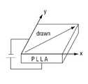
도 7 내지 도 9는 본 개시의 일 실시 예에 따른 터치 패드에 사용되는 압전 필름의 변형 방향을 설명하기 위한 도면이다. 구체적으로, 압전 필름은 PLA 재질로 구성될 수 있다.7 to 9 are views for explaining a deformation direction of a piezoelectric film used in a touch pad according to an exemplary embodiment of the present disclosure. Specifically, the piezoelectric film may be made of PLA material.
도 7을 참조하면, 드로잉 방향(drawing direction)이 x축 방향인 압전 필름(800)에 전압을 가하는 경우, 전압에 의해 드로잉 방향과 45˚를 이루는 방향으로 늘어나는 형태로 변형되는 압전 필름(801)을 얻을 수 있다. 이 때, 드로잉 방향은 압전 필름 롤(roll)을 제조한 경우, 압전 필름 롤을 풀어낼 때의 힘의 방향을 의미한다. 즉, 드로잉 방향은 압전 필름 롤의 축과 수직인 방향 중 어느 하나일 수 있다.Referring to FIG. 7 , when a voltage is applied to the
도 8은 드로잉 방향과 45˚를 이루는 방향으로 재단한 압전 필름의 변형 형태를 도시한 도면이다.8 is a view showing a deformed form of a piezoelectric film cut in a direction forming 45 degrees with a drawing direction.
도 8을 참조하면, 드로잉 방향과 45˚를 이루는 방향으로 재단된 압전 필름(800)의 한쪽 에지를 고정하고 전압을 가하는 경우, 전압에 의해 변형된 압전 필름(802)은 고정하지 않은 반대쪽 에지가 아래(또는 위)로 휘는 벤딩 형태의 변형이 일어날 수 있다.Referring to FIG. 8 , when one edge of the
도 9는 드로잉 방향으로 재단한 압전 필름의 변형 형태를 도시한 도면이다.9 is a view showing a deformed form of a piezoelectric film cut in a drawing direction.
도 9를 참조하면, 드로잉 방향으로 재단한 압전 필름(800)의 한쪽 에지를 고정하고 전압을 가하는 경우, 전압에 의해 변형된 압전 필름(803)은 고정하지 않은 반대쪽 에지의 양 끝이 아래(또는 위)로 휘는 트위스트 형태의 변형이 일어날 수 있다.Referring to FIG. 9 , when one edge of the
도 7 내지 도 9에서 살펴본 바와 같이, 압전 필름에 전압을 가할 때, 압전 필름은 재단 방향에 따라 다양한 형태로 변형할 수 있다. 이를 이용하여, 전자 장치는 터치의 강도 뿐만 아니라, 단순 누르는 터치 또는 눌러서 비트는 터치 등 다양한 터치의 형태를 구분할 수 있다.As shown in FIGS. 7 to 9 , when a voltage is applied to the piezoelectric film, the piezoelectric film may be deformed in various shapes depending on the cutting direction. Using this, the electronic device can distinguish not only the strength of the touch, but also various types of touch, such as a simple pressing touch or a pressing and twisting touch.
도 10 내지 도 15는 터치 패드에 사용되는 복수의 투명 압전 필름을 적층하는 방법에 대한 다양한 실시 예를 설명하기 위한 도면이다.10 to 15 are views for explaining various embodiments of a method of laminating a plurality of transparent piezoelectric films used in a touch pad.
구체적으로 도 10 및 도 11은 거울상 이성질체인 PLLA 필름과 PDLA 필름을 교차 적층하여 투명 압전 필름층을 생성하는 방법을 설명하기 위한 도면이다.Specifically, FIGS. 10 and 11 are diagrams for explaining a method of generating a transparent piezoelectric film layer by cross-laminating an enantiomeric PLLA film and a PDLA film.
도 11을 참조하면, 투명 압전 필름층은 복수의 PLLA 필름 및 PDLA 필름을 교차 적층하여 생성할 수 있다. 구체적으로, 투명 압전 필름층은 도 10에 도시된 바와 같이, 투명 압전 필름층은 PDLA 필름과 PLLA 필름의 드로잉 방향을 맞추어 적층할 수 있다.Referring to FIG. 11 , the transparent piezoelectric film layer may be formed by cross-laminating a plurality of PLLA films and PDLA films. Specifically, as shown in FIG. 10 , the transparent piezoelectric film layer may be stacked in alignment with the drawing direction of the PDLA film and the PLLA film.
이로 인해, 투명 압전 필름층의 접촉 압력 센싱 정밀도를 향상할 수 있다. 구체적으로, 적은 힘을 가하더라도 많은 전압이 발생하거나, 적은 전압을 인가하여도 많은 진동을 발생시킬 수 있다. 또한, 터치 스크린을 누르는 힘의 변화가 적더라도 발생되는 전압의 변화는 커져, 전자 장치는 터치의 강도를 보다 여러 단계로 나누어 판단할 수 있다. 다른 실시 예로, 터치 스크린에 터치 압력이 발생될 경우에, 전압이 발생되는 복수의 필름층 및 각 필름층에서 발생되는 전압을 크기로 터치 압력의 강도를 세분하여 구할 수 있다.Accordingly, the contact pressure sensing precision of the transparent piezoelectric film layer may be improved. Specifically, a large voltage may be generated even when a small force is applied, or a large amount of vibration may be generated even when a small voltage is applied. In addition, even if the change in the force pressing the touch screen is small, the change in the generated voltage is large, so the electronic device can determine the strength of the touch by dividing it into several stages. In another embodiment, when a touch pressure is generated on the touch screen, the strength of the touch pressure may be obtained by subdividing the voltage generated in a plurality of film layers and the voltage generated in each film layer.
한편, 도 12 내지 도 15는 복수의 PLLA 필름을 적층하여 투명 압전 필름층을 생성하는 방법을 설명하기 위한 도면이다. 구체적으로, 도 12 내지 도 14에는, 복수의 PLLA 필름을 적층하기 위하여 드로잉 방향을 맞추는 방법이 도시되어 있다. 도 12 내지 도 14의 PLLA 필름에 기재된 'PLLA'는 압전 필름의 종류 및 방향을 나타내기 위해 기재된 것일 뿐, 실제 구현시에는 기재되지 않을 수 있다.Meanwhile, FIGS. 12 to 15 are views for explaining a method of generating a transparent piezoelectric film layer by laminating a plurality of PLLA films. Specifically, in FIGS. 12 to 14, a method of aligning the drawing direction in order to laminate a plurality of PLLA films is shown. 'PLLA' described in the PLLA film of FIGS. 12 to 14 is only described to indicate the type and direction of the piezoelectric film, and may not be described in actual implementation.
도 12을 참조하면, PLLA 필름의 드로잉 방향은 PLLA 필름이 놓인 xy 평면 상에 있을 수 있다. 예를 들어, 'PLLA'라고 기재된 정면에 x축이 위치하고, 양 측면 중 어느 한 면에 y축이 위치한다고 가정하면, PLLA 필름의 드로잉 방향은 xy 평면 상에 놓일 수 있다.Referring to FIG. 12 , the drawing direction of the PLLA film may be on the xy plane on which the PLLA film is placed. For example, assuming that the x-axis is located on the front side written 'PLLA' and the y-axis is located on either side, the drawing direction of the PLLA film may lie on the xy plane.
이 때, y축을 축으로 하여 PLLA 필름을 뒤집으면, 도 13에 도시된 바와 같이 'PLLA'가 거꾸로 기재되고, 드로잉 방향은 도 12의 드로잉 방향과 y축을 중심으로 대칭이게 된다.At this time, when the PLLA film is turned over with respect to the y-axis, 'PLLA' is written upside down as shown in FIG. 13, and the drawing direction is symmetrical about the drawing direction of FIG. 12 and the y-axis.
이후, 도 13에 도시된 PLLA 필름을 시계 방향으로 90˚ 회전하면, 도 14에 도시된 바와 같이, 도 12에 도시된 PLLA 필름과 드로잉 방향이 일치하게 된다.Thereafter, when the PLLA film shown in FIG. 13 is rotated clockwise by 90°, as shown in FIG. 14, the drawing direction coincides with the PLLA film shown in FIG. 12.
한편 설명의 편의를 위하여 PLLA 필름을 y축을 중심으로 뒤집은 후 시계 방향으로 90˚ 회전하여 드로잉 방향을 일치시키는 것으로 한정하고 도시하여 설명하였으나, 실제 구현시에는 x축을 중심으로 뒤집은 후 반시계 방향으로 90˚ 회전하여 드로잉 방향을 일치시키는 등 다양한 방법으로 구현할 수도 있다.On the other hand, for convenience of explanation, the PLLA film was flipped around the y-axis and then rotated clockwise by 90 degrees to match the drawing direction. It can be implemented in various ways, such as rotating it ˚ to match the drawing direction.
그 다음, 도 12에 도시된 PLLA 필름 및 도 14에 도시된 PLLA 필름을 교차 적층하면, 도 15에 도시된 바와 같이 복수의 PLLA 필름을 이용한 투명 압전 필름층을 생성할 수 있다.Then, when the PLLA film shown in FIG. 12 and the PLLA film shown in FIG. 14 are cross-laminated, a transparent piezoelectric film layer using a plurality of PLLA films can be created as shown in FIG. 15 .
한편, 도 15에는 설명의 편의를 위하여 'PLLA'가 기재된 면과 'PLLA'가 거꾸로 기재된 면이 동일한 면에 위치하는 것으로 도시하고 설명하였으나, 실제 구현시에는, 'PLLA'가 기재된 면은 도 12에 도시된 바와 같이 정면에, 'PLLA'가 거꾸로 기재된 면은 도 14에 도시된 바와 같이, 오른쪽 측면에 위치하도록 적층될 것이다.Meanwhile, in FIG. 15, for convenience of description, the side on which 'PLLA' is written and the side on which 'PLLA' is written backwards are shown and described as being located on the same side, but in actual implementation, the side on which 'PLLA' is written is shown in FIG. As shown in FIG. 14, the side on which 'PLLA' is written backwards on the front side will be stacked so as to be located on the right side as shown in FIG.
한편, 도 12 내지 도 15에서는 설명의 편의를 위하여 복수의 PLLA 필름만을 적층하여 투명 압전 필름층을 생성하는 것으로 한정하여 도시하고 설명하였으나, 실제 구현시에는 동일한 방법으로 PDLA 필름을 적층하여 투명 압전 필름층을 생성하는 것으로 구현할 수도 있다.Meanwhile, in FIGS. 12 to 15, for convenience of description, only a plurality of PLLA films are laminated to form a transparent piezoelectric film layer, but in actual implementation, PDLA films are laminated in the same way to form a transparent piezoelectric film. It can also be implemented by creating layers.
이로 인해, 투명 압전 필름층의 접촉 압력 센싱 감도(sensitivity)를 향상할 수 있다. 구체적으로, 투명 압전 필름층을 복수의 필름을 적층하여 구성한 경우, 하나의 필름으로 구성된 것과 비교하여, 동일한 힘을 가하더라도 발생되는 전기 신호의 전압의 크기가 커지므로, 터치 스크린은 보다 미세한 접촉 압력을 감지할 수 있고, 동일한 전압을 인가하면, 더 큰 진동을 발생시킬 수 있다. 또한, 터치 스크린을 누르는 힘의 변화가 적더라도 발생되는 전기 신호의 전압의 변화는 커져, 전자 장치는 터치의 강도를 보다 미세하게 나누어 판단할 수 있다.Accordingly, the contact pressure sensing sensitivity of the transparent piezoelectric film layer may be improved. Specifically, when the transparent piezoelectric film layer is formed by laminating a plurality of films, the magnitude of the voltage of the electric signal generated even when the same force is applied is increased compared to a case composed of one film, so that the touch screen has a finer contact pressure can be sensed, and if the same voltage is applied, a larger vibration can be generated. In addition, even if the change in force pressing the touch screen is small, the change in the voltage of the generated electrical signal is large, so that the electronic device can determine the strength of the touch by dividing it more finely.
한편, 이상에서는 복수의 필름을 적층한 투명 압전 필름층 전체에서 발생하는 전기 신호의 전압을 감지하여 접촉 압력의 크기를 판단하는 것으로 한정하여 설명하였으나, 실제 구현시에는, 투명 압전 필름층을 구성하는 복수의 필름 각각에서 발생되는 각 전기 신호의 전압을 감지하여 접촉 압력의 크기를 판단하는 형식으로 구현될 수 있다.Meanwhile, in the above description, the voltage of an electrical signal generated in the entire transparent piezoelectric film layer in which a plurality of films are stacked is limited to determining the magnitude of the contact pressure, but in actual implementation, the transparent piezoelectric film layer constituting the It may be implemented in a form of determining the magnitude of the contact pressure by sensing the voltage of each electrical signal generated from each of the plurality of films.
이상과 같이 본 개시의 다양한 실시 예에 따르면, 터치의 강도를 구분하여 인식할 수 있고, 터치 영역의 국부적인 진동이 가능하여 소비 전력이 감소하며, 터치의 감도가 향상되어 누르는 힘이 적어도 터치를 인식할 수 있는 전자 장치를 제공하여, 사용자의 편의를 향상시킬 수 있다.As described above, according to various embodiments of the present disclosure, it is possible to distinguish and recognize the intensity of touch, local vibration of the touch area is possible, reducing power consumption, and improving touch sensitivity, so that the pressing force is minimal. A user's convenience may be improved by providing a recognizable electronic device.
이상과 같이 본 개시는 비록 한정된 예시적 실시 예와 도면에 의해 설명되었으나, 본 개시는 상기의 예시적 실시 예에 한정되는 것은 아니며, 본 개시가 속하는 분야에서 통상의 지식을 가진 자라면 이러한 기재로부터 다양한 수정 및 변형이 가능하다.As described above, although the present disclosure has been described with limited exemplary embodiments and drawings, the present disclosure is not limited to the above exemplary embodiments, and those skilled in the art in the field to which the present disclosure belongs will learn from these descriptions. Many modifications and variations are possible.
그러므로, 본 개시의 범위는 설명된 예시적 실시 예에 국한되어 정해져서는 아니 되며, 후술하는 특허청구범위뿐 아니라 이 특허청구범위와 균등한 것들에 의해 정해져야 한다.Therefore, the scope of the present disclosure should not be limited to the described exemplary embodiments and should not be defined, and should be defined by not only the claims to be described later, but also those equivalent to these claims.
100 : 전자 장치
110 : 터치 스크린
111 : 디스플레이 패널
112 : 터치 패드
113 : 윈도우 커버
120 : 프로세서100: electronic device
110: touch screen
111: display panel
112: touch pad
113: window cover
120: processor
Claims (20)
Translated fromKorean투명 압전 필름층; 및
상기 투명 압전 필름층 상의 복수의 영역에 배치된 복수의 투명 전극을 포함하는 전극층;을 포함하고,
상기 전극층은,
상기 투명 압전 필름층 상에서의 터치 압력에 의해 생성되는 제1 전압을 감지하는 복수의 제1 투명 전극, 및
상기 투명 압전 필름 층에 제2 전압을 인가하는 복수의 제2 투명 전극을 포함하고,
상기 복수의 제1 투명 전극 및 상기 복수의 제2 투명 전극은 상기 투명 압전 필름층 상부 면에 동일한 방향의 라인 형태로 일렬로 배치되는 터치 패드.In the touch pad,
a transparent piezoelectric film layer; and
An electrode layer including a plurality of transparent electrodes disposed in a plurality of regions on the transparent piezoelectric film layer;
The electrode layer,
A plurality of first transparent electrodes sensing a first voltage generated by a touch pressure on the transparent piezoelectric film layer, and
And a plurality of second transparent electrodes for applying a second voltage to the transparent piezoelectric film layer,
The plurality of first transparent electrodes and the plurality of second transparent electrodes are arranged in a line in the form of lines in the same direction on an upper surface of the transparent piezoelectric film layer.
상기 전극층은,
상기 투명 압전 필름층 상부에, 셀 형태의 복수의 투명 전극이 매트릭스 형태로 배치된 것인 터치 패드.According to claim 1,
The electrode layer,
A touch pad wherein a plurality of cell-shaped transparent electrodes are disposed in a matrix form on the transparent piezoelectric film layer.
상기 투명 압전 필름층은,
제1 투명 압전 필름층; 및 상기 제1 투명 압전 필름층 상부에 배치된 제2 투명 압전 필름층;을 포함하고,
상기 전극층은,
상기 제1 투명 압전 필름층 상부 면에, 라인 형태의 복수의 투명 전극이 일렬로 배치된 제1 전극층; 및
상기 제2 투명 압전 필름층 상부 면에, 라인 형태의 복수의 투명 전극이 일렬로 배치된 제2 전극층;을 포함하고,
상기 제1 전극층의 상기 복수의 투명 전극과 상기 제2 전극층의 상기 복수의 투명 전극은 직교하는 형태인 터치 패드.According to claim 1,
The transparent piezoelectric film layer,
a first transparent piezoelectric film layer; and a second transparent piezoelectric film layer disposed on the first transparent piezoelectric film layer,
The electrode layer,
a first electrode layer in which a plurality of line-shaped transparent electrodes are arranged in a row on an upper surface of the first transparent piezoelectric film layer; and
A second electrode layer in which a plurality of line-shaped transparent electrodes are arranged in a row on an upper surface of the second transparent piezoelectric film layer;
The plurality of transparent electrodes of the first electrode layer and the plurality of transparent electrodes of the second electrode layer are orthogonal to each other.
상기 투명 압전 필름층은,
상기 전극층에 포함된 상기 복수의 투명 전극 중 적어도 하나의 상기 투명 전극을 통하여 전압이 인가되면, 상기 인가된 전압에 대응되는 진동을 발생시키는 터치 패드.According to claim 1,
The transparent piezoelectric film layer,
When a voltage is applied through at least one of the plurality of transparent electrodes included in the electrode layer, the touch pad generates vibration corresponding to the applied voltage.
상기 투명 압전 필름층은,
PLLA(Poly-L-Lactide Acid) 필름, PDLA(Poly-D-Lactide Acid) 필름 및 PVDF(Polyvinylidene fluoride) 필름 중 적어도 하나로 구성된 터치 패드.According to claim 1,
The transparent piezoelectric film layer,
A touch pad made of at least one of a Poly-L-Lactide Acid (PLLA) film, a Poly-D-Lactide Acid (PDLA) film, and a Polyvinylidene fluoride (PVDF) film.
상기 투명 압전 필름층은,
상기 PLLA 필름 및 상기 PDLA 필름이 교차하여 적층된 것인 터치 패드.According to claim 5,
The transparent piezoelectric film layer,
A touch pad in which the PLLA film and the PDLA film are stacked by crossing each other.
상기 투명 압전 필름층은,
상기 PLLA 필름 및 상기 PDLA 필름 중 어느 하나가 적층된 것인 터치 패드.According to claim 5,
The transparent piezoelectric film layer,
A touch pad in which any one of the PLLA film and the PDLA film is laminated.
상기 복수의 투명 전극은,
PEDOT(Poly(3,4-ethylenedioxythiophene)), CNT(Carbon Nano Tube), ITO(Indium Tin Oxide) 또는 그래핀(Graphene)으로 구성된 터치 패드.According to claim 1,
The plurality of transparent electrodes,
A touchpad made of PEDOT (Poly(3,4-ethylenedioxythiophene)), CNT (Carbon Nano Tube), ITO (Indium Tin Oxide) or Graphene.
화면을 표시하는 디스플레이 패널;
상기 디스플레이 패널 상부에 배치되는 제1항 내지 제8항 중 어느 한 항의 터치 패드; 및
상기 터치 패드의 상부에 배치되는 윈도우 커버;를 포함하는 터치 스크린.In the touch screen,
a display panel displaying a screen;
a touch pad according to any one of claims 1 to 8 disposed above the display panel; and
A touch screen including a window cover disposed above the touch pad.
제9항의 터치 스크린; 및
상기 복수의 제1 투명 전극을 통해 감지된 제1 전압에 기초하여 접촉 압력이 가해진 위치를 판단하는 프로세서;를 포함하는 전자 장치.In electronic devices,
The touch screen of claim 9; and
An electronic device comprising a; processor to determine a position to which the contact pressure is applied based on the first voltage sensed through the plurality of first transparent electrodes.
상기 프로세서는,
상기 복수의 제1 투명 전극을 통해 감지된 제1 전압의 크기에 기초하여, 상기 감지된 제1 전압의 크기에 대응되는 동작을 수행하는 전자 장치.According to claim 10,
the processor,
An electronic device that performs an operation corresponding to the detected magnitude of the first voltage based on the magnitude of the first voltage sensed through the plurality of first transparent electrodes.
투명 압전 필름층을 준비하는 단계;
상기 투명 압전 필름층 상의 복수의 영역에 배치된 복수의 투명 전극을 포함하는 전극층;을 형성하는 단계;를 포함하고,
상기 전극층은,
상기 투명 압전 필름층 상에서의 터치 압력에 의해 생성되는 제1 전압을 감지하는 복수의 제1 투명 전극, 및
상기 투명 압전 필름 층에 제2 전압을 인가하는 복수의 제2 투명 전극을 포함하고,
상기 복수의 제1 투명 전극 및 상기 복수의 제2 투명 전극은 상기 투명 압전 필름층 상부 면에 동일한 방향의 라인 형태로 일렬로 배치되는 터치 패드의 제조 방법.In the manufacturing method of the touch pad,
preparing a transparent piezoelectric film layer;
Forming an electrode layer including a plurality of transparent electrodes disposed in a plurality of regions on the transparent piezoelectric film layer,
The electrode layer,
A plurality of first transparent electrodes sensing a first voltage generated by a touch pressure on the transparent piezoelectric film layer, and
And a plurality of second transparent electrodes for applying a second voltage to the transparent piezoelectric film layer,
The plurality of first transparent electrodes and the plurality of second transparent electrodes are disposed in a line in the form of lines in the same direction on the upper surface of the transparent piezoelectric film layer.
상기 복수의 투명 전극을 포함하는 전극층을 형성하는 단계는,
상기 투명 압전 필름층 상부에 전극층을 증착하는 단계;
상기 복수의 투명 전극 영역을 정의하는 패턴을 상기 증착된 전극층 상부에 형성하는 단계; 및
상기 복수의 투명 전극 영역 이외의 영역을 에칭하는 단계;를 포함하는 터치 패드의 제조 방법.According to claim 12,
Forming an electrode layer including the plurality of transparent electrodes,
depositing an electrode layer on top of the transparent piezoelectric film layer;
forming a pattern defining the plurality of transparent electrode regions on the deposited electrode layer; and
and etching an area other than the plurality of transparent electrode areas.
상기 패턴은,
상기 투명 압전 필름층 상부에 셀 형태의 복수의 투명 전극이 매트릭스 형태로 배열되도록 상기 복수의 투명 전극 영역을 정의하는 것인 터치 패드의 제조 방법.According to claim 13,
The pattern is
and defining the plurality of transparent electrode regions so that the plurality of cell-shaped transparent electrodes are arranged in a matrix form on the transparent piezoelectric film layer.
상기 패턴은,
상기 투명 압전 필름층 상부에 라인 형태의 복수의 투명 전극이 일렬로 배열되도록 상기 복수의 투명 전극 영역을 정의하는 것인 터치 패드의 제조 방법.According to claim 13,
The pattern is
and defining the plurality of transparent electrode regions such that a plurality of line-shaped transparent electrodes are arranged in a line on the transparent piezoelectric film layer.
상기 투명 압전 필름층을 준비하는 단계는,
제1 투명 압전 필름층 및 제2 투명 압전 필름층을 준비하는 단계;를 포함하고,
상기 제1 투명 압전 필름층 상부에 형성된 상기 복수의 투명 전극과 상기 제2 투명 압전 필름층 상부에 형성된 상기 복수의 투명 전극이 직교하도록 상기 제1 투명 압전 필름층 및 상기 제2 투명 압전 필름층을 배치하는 단계;를 더 포함하는 터치 패드의 제조 방법.According to claim 15,
Preparing the transparent piezoelectric film layer,
Preparing a first transparent piezoelectric film layer and a second transparent piezoelectric film layer; Including,
The first transparent piezoelectric film layer and the second transparent piezoelectric film layer are formed such that the plurality of transparent electrodes formed on the first transparent piezoelectric film layer and the plurality of transparent electrodes formed on the second transparent piezoelectric film layer are orthogonal to each other. A method of manufacturing a touch pad further comprising; disposing.
상기 투명 압전 필름층은,
PLLA(Poly-L-Lactide Acid) 필름, PDLA(Poly-D-Lactide Acid) 필름 및 PVDF(Polyvinylidene fluoride) 필름 중 적어도 하나로 구성된 터치 패드의 제조 방법.According to claim 12,
The transparent piezoelectric film layer,
A method for manufacturing a touch pad composed of at least one of a poly-L-lactide acid (PLLA) film, a poly-D-lactide acid (PDLA) film, and a polyvinylidene fluoride (PVDF) film.
상기 투명 압전 필름층을 준비하는 단계는,
상기 PLLA 필름 및 상기 PDLA 필름이 교차하여 적층하는 단계;를 포함하는 터치 패드의 제조 방법.According to claim 17,
Preparing the transparent piezoelectric film layer,
A method of manufacturing a touch pad comprising: crossing and stacking the PLLA film and the PDLA film.
상기 투명 압전 필름층을 준비하는 단계는,
상기 PLLA 필름 및 상기 PDLA 필름 중 어느 하나를 적층하는 단계;를 포함하는 터치 패드의 제조 방법.According to claim 17,
Preparing the transparent piezoelectric film layer,
A method of manufacturing a touch pad comprising: laminating one of the PLLA film and the PDLA film.
상기 복수의 투명 전극은,
PEDOT(Poly(3,4-ethylenedioxythiophene)), CNT(Carbon Nano Tube), ITO(Indium Tin Oxide) 또는 그래핀(Graphene)으로 구성된 터치 패드의 제조 방법.According to claim 12,
The plurality of transparent electrodes,
A method for manufacturing a touch pad composed of PEDOT (Poly (3,4-ethylenedioxythiophene)), CNT (Carbon Nano Tube), ITO (Indium Tin Oxide) or graphene.
Priority Applications (2)
| Application Number | Priority Date | Filing Date | Title |
|---|---|---|---|
| US15/277,282US10635222B2 (en) | 2015-10-02 | 2016-09-27 | Touch pad and electronic apparatus using the same, and method of producing touch pad |
| PCT/KR2016/010945WO2017057938A1 (en) | 2015-10-02 | 2016-09-30 | Touch pad, and touch screen and electronic device using same, and touch pad manufacturing method |
Applications Claiming Priority (2)
| Application Number | Priority Date | Filing Date | Title |
|---|---|---|---|
| US201562236535P | 2015-10-02 | 2015-10-02 | |
| US62/236,535 | 2015-10-02 |
Publications (2)
| Publication Number | Publication Date |
|---|---|
| KR20170040071A KR20170040071A (en) | 2017-04-12 |
| KR102476610B1true KR102476610B1 (en) | 2022-12-12 |
Family
ID=58580337
Family Applications (2)
| Application Number | Title | Priority Date | Filing Date |
|---|---|---|---|
| KR1020160028475AActiveKR102476610B1 (en) | 2015-10-02 | 2016-03-09 | Touch pad, touch screen and electronic apparatus using the same and method for producing touch pad |
| KR1020160040403AActiveKR102476614B1 (en) | 2015-10-02 | 2016-04-01 | Touch screen, touch panel and eletronic deivce having the same |
Family Applications After (1)
| Application Number | Title | Priority Date | Filing Date |
|---|---|---|---|
| KR1020160040403AActiveKR102476614B1 (en) | 2015-10-02 | 2016-04-01 | Touch screen, touch panel and eletronic deivce having the same |
Country Status (2)
| Country | Link |
|---|---|
| US (1) | US10698510B2 (en) |
| KR (2) | KR102476610B1 (en) |
Families Citing this family (8)
| Publication number | Priority date | Publication date | Assignee | Title |
|---|---|---|---|---|
| WO2017161586A1 (en)* | 2016-03-25 | 2017-09-28 | 华为技术有限公司 | Touch screen device, and method and apparatus for executing operation |
| WO2018038367A1 (en)* | 2016-08-26 | 2018-03-01 | 주식회사 하이딥 | Touch input device including display panel having strain gauge, and method for manufacturing display panel having strain gauge |
| KR101920440B1 (en)* | 2017-08-21 | 2018-11-20 | (주)실리콘인사이드 | Self inductive force sensor module for 3d touch implementation |
| KR101979647B1 (en) | 2017-09-19 | 2019-05-17 | 주식회사 우정하이텍 | Force touch sensor using strain gauge |
| CN107608564A (en)* | 2017-10-26 | 2018-01-19 | 武汉华星光电技术有限公司 | Contact panel and contactor control device |
| KR102728818B1 (en) | 2019-02-15 | 2024-11-12 | 삼성디스플레이 주식회사 | Input sensing circuit and display device having the same |
| KR102371459B1 (en) | 2020-05-25 | 2022-03-08 | 한국과학기술연구원 | Object recognition apparatus |
| CN117631881A (en)* | 2023-12-29 | 2024-03-01 | 武汉华星光电技术有限公司 | Touch display device and touch method thereof |
Citations (2)
| Publication number | Priority date | Publication date | Assignee | Title |
|---|---|---|---|---|
| WO2015077200A1 (en)* | 2013-11-21 | 2015-05-28 | 3M Innovative Properties Company | Multi-layer piezoelectric polymer film devices and methods |
| JP2015111391A (en)* | 2013-11-11 | 2015-06-18 | Nltテクノロジー株式会社 | Piezoelectric sheet, touch panel using the same, and input/output device using these |
Family Cites Families (41)
| Publication number | Priority date | Publication date | Assignee | Title |
|---|---|---|---|---|
| KR100595922B1 (en) | 1998-01-26 | 2006-07-05 | 웨인 웨스터만 | Method and apparatus for integrating manual input |
| US20090002199A1 (en) | 2007-06-28 | 2009-01-01 | Nokia Corporation | Piezoelectric sensing as user input means |
| US8174372B2 (en) | 2008-06-26 | 2012-05-08 | Immersion Corporation | Providing haptic feedback on a touch surface |
| KR101150158B1 (en)* | 2009-08-14 | 2012-05-25 | 주성엔지니어링(주) | Touch screen integrated display |
| US8390594B2 (en) | 2009-08-18 | 2013-03-05 | Immersion Corporation | Haptic feedback using composite piezoelectric actuator |
| KR101109226B1 (en) | 2009-12-21 | 2012-01-30 | 삼성전기주식회사 | Piezoelectric actuator module and touch screen device using same |
| US8669963B2 (en)* | 2010-02-03 | 2014-03-11 | Interlink Electronics, Inc. | Sensor system |
| KR101093615B1 (en) | 2010-03-19 | 2011-12-15 | 전자부품연구원 | 3D Sensing Panel |
| JP5216041B2 (en) | 2010-04-07 | 2013-06-19 | ダイキン工業株式会社 | Transparent piezoelectric sheet with frame, each having transparent piezoelectric sheet, touch panel, and electronic device |
| JP2011242386A (en) | 2010-04-23 | 2011-12-01 | Immersion Corp | Transparent compound piezoelectric material aggregate of contact sensor and tactile sense actuator |
| JP5813103B2 (en) | 2010-06-11 | 2015-11-17 | スリーエム イノベイティブ プロパティズ カンパニー | Touch position sensor with force measurement |
| US20120019449A1 (en) | 2010-07-26 | 2012-01-26 | Atmel Corporation | Touch sensing on three dimensional objects |
| US9569003B2 (en)* | 2010-09-30 | 2017-02-14 | Broadcom Corporation | Portable computing device including a three-dimensional touch screen |
| KR101809191B1 (en) | 2010-10-11 | 2018-01-18 | 삼성전자주식회사 | Touch panel |
| EP3686719B1 (en) | 2010-12-24 | 2024-08-14 | Graphene Square Inc. | Touch sensor using graphene for simultaneously detecting a pressure and a position |
| JP5708167B2 (en) | 2011-04-06 | 2015-04-30 | コニカミノルタ株式会社 | Ultrasonic probe and ultrasonic diagnostic apparatus |
| EP2743804B1 (en) | 2011-08-11 | 2018-11-14 | Murata Manufacturing Co., Ltd. | Touch panel |
| EP2587347A3 (en) | 2011-10-25 | 2016-01-20 | Broadcom Corporation | Portable computing device including a three-dimensional touch screen |
| TWI455004B (en) | 2011-12-20 | 2014-10-01 | Wistron Corp | Touch display panel and driving method thereof |
| KR20130085201A (en) | 2012-01-19 | 2013-07-29 | 엘지전자 주식회사 | Mobile/portable terminal |
| KR20130116167A (en) | 2012-04-12 | 2013-10-23 | 삼성전자주식회사 | Device and method for sensing 3d object |
| KR101542043B1 (en)* | 2012-06-27 | 2015-08-06 | 엘지디스플레이 주식회사 | Touch screen panel |
| WO2014008401A1 (en) | 2012-07-05 | 2014-01-09 | Northeastern University | Devices, methods, and systems for high-resolution tactile displays |
| KR101915064B1 (en) | 2012-08-23 | 2018-11-05 | 삼성전자주식회사 | Flexible device and operating methods thereof |
| EP2893423B1 (en) | 2012-09-04 | 2020-01-15 | JOANNEUM RESEARCH Forschungsgesellschaft mbH | Printed piezoelectric pressure sensing foil |
| KR101974579B1 (en) | 2012-09-05 | 2019-08-26 | 삼성전자주식회사 | Pressure sensor and method for sensing pressure by using the same |
| KR102092132B1 (en) | 2012-11-30 | 2020-04-14 | 삼성전자주식회사 | Electronic apparatus providing hovering input effect and control method thereof |
| WO2014098946A1 (en) | 2012-12-17 | 2014-06-26 | Changello Enterprise Llc | Force detection in touch devices using piezoelectric sensors |
| KR102051518B1 (en) | 2013-01-28 | 2019-12-03 | 삼성전자주식회사 | Energy harvesting device combined with self-powered touch sensor |
| US9489047B2 (en) | 2013-03-01 | 2016-11-08 | Immersion Corporation | Haptic device with linear resonant actuator |
| KR101526043B1 (en) | 2013-03-04 | 2015-06-04 | 울산대학교 산학협력단 | Haptic feedback screen using piezoelectric polymers |
| KR102082425B1 (en) | 2013-06-10 | 2020-02-28 | 삼성디스플레이 주식회사 | Flat panel display device |
| KR20150032028A (en) | 2013-09-16 | 2015-03-25 | 유재천 | Three dimensional space-touch screen apparatus and method using the same |
| WO2015060280A1 (en) | 2013-10-25 | 2015-04-30 | 株式会社村田製作所 | Electronic device and manipulation input program |
| KR102086402B1 (en) | 2013-11-06 | 2020-03-09 | 엘지디스플레이 주식회사 | Touch screen panel and display apparatus |
| WO2015068709A1 (en) | 2013-11-08 | 2015-05-14 | 株式会社村田製作所 | Display device and program |
| US20160299606A1 (en) | 2013-12-05 | 2016-10-13 | Widevantage Inc. | User input processing device using limited number of magnetic field sensors |
| EP4071589A1 (en) | 2013-12-12 | 2022-10-12 | QUALCOMM Incorporated | Micromechanical ultrasonic transducers and display |
| KR101457336B1 (en)* | 2014-02-21 | 2014-11-13 | 주식회사 트레이스 | Touch screen integrated digitizer using 3 dimensional magnetism sensor and magnetic pen |
| JP2015162153A (en) | 2014-02-28 | 2015-09-07 | 京セラドキュメントソリューションズ株式会社 | Touch panel device and image forming apparatus |
| US10353500B2 (en) | 2015-01-27 | 2019-07-16 | Lg Innotek Co., Ltd. | Touch device |
- 2016
- 2016-03-09KRKR1020160028475Apatent/KR102476610B1/enactiveActive
- 2016-04-01KRKR1020160040403Apatent/KR102476614B1/enactiveActive
- 2016-09-29USUS15/764,590patent/US10698510B2/ennot_activeExpired - Fee Related
Patent Citations (2)
| Publication number | Priority date | Publication date | Assignee | Title |
|---|---|---|---|---|
| JP2015111391A (en)* | 2013-11-11 | 2015-06-18 | Nltテクノロジー株式会社 | Piezoelectric sheet, touch panel using the same, and input/output device using these |
| WO2015077200A1 (en)* | 2013-11-21 | 2015-05-28 | 3M Innovative Properties Company | Multi-layer piezoelectric polymer film devices and methods |
Also Published As
| Publication number | Publication date |
|---|---|
| KR102476614B1 (en) | 2022-12-13 |
| KR20170040076A (en) | 2017-04-12 |
| US20180284915A1 (en) | 2018-10-04 |
| US10698510B2 (en) | 2020-06-30 |
| KR20170040071A (en) | 2017-04-12 |
Similar Documents
| Publication | Publication Date | Title |
|---|---|---|
| KR102476610B1 (en) | Touch pad, touch screen and electronic apparatus using the same and method for producing touch pad | |
| US9052787B2 (en) | Method of manufacturing touch sensing apparatus | |
| KR101521681B1 (en) | Touch Panel | |
| US20140293151A1 (en) | Touch Panel and Manufacturing Method Thereof | |
| KR101103751B1 (en) | Touch screen panel with mesh type electrode pattern | |
| US20120162099A1 (en) | Touch screen | |
| US20120018200A1 (en) | Transparent conductive film for touch panel and method for manufacturing the same | |
| US10394339B2 (en) | Sensor, input device, keyboard, and electronic device | |
| CN104281306B (en) | Touch control type display device and manufacturing method thereof | |
| US10379641B2 (en) | Touch screen apparatus having additional sensing electrode located in non-active area | |
| TW201633070A (en) | Input device, sensor, keyboard and electronic instrument | |
| US10234959B2 (en) | Input apparatus, keyboard, and electronic apparatus | |
| US20120081329A1 (en) | Digital resistive type touch panel | |
| US20150122625A1 (en) | Touch screen panel and display device | |
| JP2014081910A (en) | Touch panel and manufacturing method of the same | |
| US8686309B2 (en) | Touch panel having conductive zone for avoiding false operation | |
| US20140009435A1 (en) | Hybrid touch panel | |
| US20140253826A1 (en) | Touch screen and manufacturing method thereof | |
| US20140125624A1 (en) | Touch screen panel and portable electronic apparatus having the same | |
| US10635222B2 (en) | Touch pad and electronic apparatus using the same, and method of producing touch pad | |
| US20180164919A1 (en) | Touch sensor and display device including the same | |
| US20140253824A1 (en) | Touch panel and manufacturing method thereof | |
| US20140253825A1 (en) | Touch panel and manufacturing method thereof | |
| US20120118606A1 (en) | Conductive film and manufacturing method thereof | |
| KR20160080069A (en) | Touch panel and display device including the same |
Legal Events
| Date | Code | Title | Description |
|---|---|---|---|
| PA0109 | Patent application | Patent event code:PA01091R01D Comment text:Patent Application Patent event date:20160309 | |
| PG1501 | Laying open of application | ||
| A201 | Request for examination | ||
| PA0201 | Request for examination | Patent event code:PA02012R01D Patent event date:20210308 Comment text:Request for Examination of Application Patent event code:PA02011R01I Patent event date:20160309 Comment text:Patent Application | |
| E902 | Notification of reason for refusal | ||
| PE0902 | Notice of grounds for rejection | Comment text:Notification of reason for refusal Patent event date:20220603 Patent event code:PE09021S01D | |
| E701 | Decision to grant or registration of patent right | ||
| PE0701 | Decision of registration | Patent event code:PE07011S01D Comment text:Decision to Grant Registration Patent event date:20220926 | |
| GRNT | Written decision to grant | ||
| PR0701 | Registration of establishment | Comment text:Registration of Establishment Patent event date:20221207 Patent event code:PR07011E01D | |
| PR1002 | Payment of registration fee | Payment date:20221208 End annual number:3 Start annual number:1 | |
| PG1601 | Publication of registration |