KR102476138B1 - Connector, light source module and light source module array using the same - Google Patents
Connector, light source module and light source module array using the sameDownload PDFInfo
- Publication number
- KR102476138B1 KR102476138B1KR1020150116838AKR20150116838AKR102476138B1KR 102476138 B1KR102476138 B1KR 102476138B1KR 1020150116838 AKR1020150116838 AKR 1020150116838AKR 20150116838 AKR20150116838 AKR 20150116838AKR 102476138 B1KR102476138 B1KR 102476138B1
- Authority
- KR
- South Korea
- Prior art keywords
- light source
- source module
- connectors
- connector
- disposed
- Prior art date
- Legal status (The legal status is an assumption and is not a legal conclusion. Google has not performed a legal analysis and makes no representation as to the accuracy of the status listed.)
- Active
Links
- 230000008878couplingEffects0.000claimsabstractdescription16
- 238000010168coupling processMethods0.000claimsabstractdescription16
- 238000005859coupling reactionMethods0.000claimsabstractdescription16
- 238000005476solderingMethods0.000claimsdescription20
- 238000013459approachMethods0.000claimsdescription3
- 238000004519manufacturing processMethods0.000description15
- 239000004065semiconductorSubstances0.000description8
- 230000008901benefitEffects0.000description6
- 238000003825pressingMethods0.000description6
- 238000000034methodMethods0.000description5
- 239000000463materialSubstances0.000description4
- 239000011347resinSubstances0.000description4
- 229920005989resinPolymers0.000description4
- 230000004888barrier functionEffects0.000description3
- 238000006243chemical reactionMethods0.000description3
- 230000000694effectsEffects0.000description3
- 150000004767nitridesChemical class0.000description3
- 239000000758substrateSubstances0.000description3
- 230000008859changeEffects0.000description2
- 230000014509gene expressionEffects0.000description2
- 238000001746injection mouldingMethods0.000description2
- 238000003780insertionMethods0.000description2
- 230000037431insertionEffects0.000description2
- 239000012212insulatorSubstances0.000description2
- 229910052751metalInorganic materials0.000description2
- 239000002184metalSubstances0.000description2
- 238000000465mouldingMethods0.000description2
- 230000008569processEffects0.000description2
- 239000002096quantum dotSubstances0.000description2
- 230000004044responseEffects0.000description2
- 229910052710siliconInorganic materials0.000description2
- JYEUMXHLPRZUAT-UHFFFAOYSA-N1,2,3-triazineChemical compoundC1=CN=NN=C1JYEUMXHLPRZUAT-UHFFFAOYSA-N0.000description1
- 229910018072Al 2 O 3Inorganic materials0.000description1
- 229910002704AlGaNInorganic materials0.000description1
- 239000004593EpoxySubstances0.000description1
- 229910002601GaNInorganic materials0.000description1
- 229910001218Gallium arsenideInorganic materials0.000description1
- OAICVXFJPJFONN-UHFFFAOYSA-NPhosphorusChemical compound[P]OAICVXFJPJFONN-UHFFFAOYSA-N0.000description1
- 239000004642PolyimideSubstances0.000description1
- 230000004308accommodationEffects0.000description1
- 238000003491arrayMethods0.000description1
- 238000005452bendingMethods0.000description1
- 230000009286beneficial effectEffects0.000description1
- 229910010293ceramic materialInorganic materials0.000description1
- 239000003086colorantSubstances0.000description1
- 238000010586diagramMethods0.000description1
- 238000003912environmental pollutionMethods0.000description1
- QSHDDOUJBYECFT-UHFFFAOYSA-NmercuryChemical compound[Hg]QSHDDOUJBYECFT-UHFFFAOYSA-N0.000description1
- 229910052753mercuryInorganic materials0.000description1
- 150000002736metal compoundsChemical class0.000description1
- 230000004048modificationEffects0.000description1
- 238000012986modificationMethods0.000description1
- 229910003465moissaniteInorganic materials0.000description1
- 230000000149penetrating effectEffects0.000description1
- 229920001721polyimidePolymers0.000description1
- 230000006798recombinationEffects0.000description1
- 238000005215recombinationMethods0.000description1
- 238000011160researchMethods0.000description1
- 229910052594sapphireInorganic materials0.000description1
- 239000010980sapphireSubstances0.000description1
- 238000007789sealingMethods0.000description1
- SBIBMFFZSBJNJF-UHFFFAOYSA-Nselenium;zincChemical compound[Se]=[Zn]SBIBMFFZSBJNJF-UHFFFAOYSA-N0.000description1
- 238000004904shorteningMethods0.000description1
- 239000010703siliconSubstances0.000description1
- 229910010271silicon carbideInorganic materials0.000description1
- 229910052596spinelInorganic materials0.000description1
- 239000011029spinelSubstances0.000description1
- 238000006467substitution reactionMethods0.000description1
- 229910052725zincInorganic materials0.000description1
Images


Classifications
- F—MECHANICAL ENGINEERING; LIGHTING; HEATING; WEAPONS; BLASTING
- F21—LIGHTING
- F21V—FUNCTIONAL FEATURES OR DETAILS OF LIGHTING DEVICES OR SYSTEMS THEREOF; STRUCTURAL COMBINATIONS OF LIGHTING DEVICES WITH OTHER ARTICLES, NOT OTHERWISE PROVIDED FOR
- F21V17/00—Fastening of component parts of lighting devices, e.g. shades, globes, refractors, reflectors, filters, screens, grids or protective cages
- F21V17/10—Fastening of component parts of lighting devices, e.g. shades, globes, refractors, reflectors, filters, screens, grids or protective cages characterised by specific fastening means or way of fastening
- F21V17/16—Fastening of component parts of lighting devices, e.g. shades, globes, refractors, reflectors, filters, screens, grids or protective cages characterised by specific fastening means or way of fastening by deformation of parts; Snap action mounting
- G—PHYSICS
- G02—OPTICS
- G02F—OPTICAL DEVICES OR ARRANGEMENTS FOR THE CONTROL OF LIGHT BY MODIFICATION OF THE OPTICAL PROPERTIES OF THE MEDIA OF THE ELEMENTS INVOLVED THEREIN; NON-LINEAR OPTICS; FREQUENCY-CHANGING OF LIGHT; OPTICAL LOGIC ELEMENTS; OPTICAL ANALOGUE/DIGITAL CONVERTERS
- G02F1/00—Devices or arrangements for the control of the intensity, colour, phase, polarisation or direction of light arriving from an independent light source, e.g. switching, gating or modulating; Non-linear optics
- G02F1/01—Devices or arrangements for the control of the intensity, colour, phase, polarisation or direction of light arriving from an independent light source, e.g. switching, gating or modulating; Non-linear optics for the control of the intensity, phase, polarisation or colour
- G02F1/13—Devices or arrangements for the control of the intensity, colour, phase, polarisation or direction of light arriving from an independent light source, e.g. switching, gating or modulating; Non-linear optics for the control of the intensity, phase, polarisation or colour based on liquid crystals, e.g. single liquid crystal display cells
- G02F1/133—Constructional arrangements; Operation of liquid crystal cells; Circuit arrangements
- G02F1/1333—Constructional arrangements; Manufacturing methods
- G02F1/1335—Structural association of cells with optical devices, e.g. polarisers or reflectors
- G02F1/1336—Illuminating devices
- F—MECHANICAL ENGINEERING; LIGHTING; HEATING; WEAPONS; BLASTING
- F21—LIGHTING
- F21K—NON-ELECTRIC LIGHT SOURCES USING LUMINESCENCE; LIGHT SOURCES USING ELECTROCHEMILUMINESCENCE; LIGHT SOURCES USING CHARGES OF COMBUSTIBLE MATERIAL; LIGHT SOURCES USING SEMICONDUCTOR DEVICES AS LIGHT-GENERATING ELEMENTS; LIGHT SOURCES NOT OTHERWISE PROVIDED FOR
- F21K9/00—Light sources using semiconductor devices as light-generating elements, e.g. using light-emitting diodes [LED] or lasers
- F—MECHANICAL ENGINEERING; LIGHTING; HEATING; WEAPONS; BLASTING
- F21—LIGHTING
- F21S—NON-PORTABLE LIGHTING DEVICES; SYSTEMS THEREOF; VEHICLE LIGHTING DEVICES SPECIALLY ADAPTED FOR VEHICLE EXTERIORS
- F21S2/00—Systems of lighting devices, not provided for in main groups F21S4/00 - F21S10/00 or F21S19/00, e.g. of modular construction
- F21S2/005—Systems of lighting devices, not provided for in main groups F21S4/00 - F21S10/00 or F21S19/00, e.g. of modular construction of modular construction
- F—MECHANICAL ENGINEERING; LIGHTING; HEATING; WEAPONS; BLASTING
- F21—LIGHTING
- F21V—FUNCTIONAL FEATURES OR DETAILS OF LIGHTING DEVICES OR SYSTEMS THEREOF; STRUCTURAL COMBINATIONS OF LIGHTING DEVICES WITH OTHER ARTICLES, NOT OTHERWISE PROVIDED FOR
- F21V15/00—Protecting lighting devices from damage
- F21V15/01—Housings, e.g. material or assembling of housing parts
- F—MECHANICAL ENGINEERING; LIGHTING; HEATING; WEAPONS; BLASTING
- F21—LIGHTING
- F21V—FUNCTIONAL FEATURES OR DETAILS OF LIGHTING DEVICES OR SYSTEMS THEREOF; STRUCTURAL COMBINATIONS OF LIGHTING DEVICES WITH OTHER ARTICLES, NOT OTHERWISE PROVIDED FOR
- F21V17/00—Fastening of component parts of lighting devices, e.g. shades, globes, refractors, reflectors, filters, screens, grids or protective cages
- F21V17/10—Fastening of component parts of lighting devices, e.g. shades, globes, refractors, reflectors, filters, screens, grids or protective cages characterised by specific fastening means or way of fastening
- F21V17/16—Fastening of component parts of lighting devices, e.g. shades, globes, refractors, reflectors, filters, screens, grids or protective cages characterised by specific fastening means or way of fastening by deformation of parts; Snap action mounting
- F21V17/164—Fastening of component parts of lighting devices, e.g. shades, globes, refractors, reflectors, filters, screens, grids or protective cages characterised by specific fastening means or way of fastening by deformation of parts; Snap action mounting the parts being subjected to bending, e.g. snap joints
- F—MECHANICAL ENGINEERING; LIGHTING; HEATING; WEAPONS; BLASTING
- F21—LIGHTING
- F21V—FUNCTIONAL FEATURES OR DETAILS OF LIGHTING DEVICES OR SYSTEMS THEREOF; STRUCTURAL COMBINATIONS OF LIGHTING DEVICES WITH OTHER ARTICLES, NOT OTHERWISE PROVIDED FOR
- F21V23/00—Arrangement of electric circuit elements in or on lighting devices
- F21V23/003—Arrangement of electric circuit elements in or on lighting devices the elements being electronics drivers or controllers for operating the light source, e.g. for a LED array
- F21V23/004—Arrangement of electric circuit elements in or on lighting devices the elements being electronics drivers or controllers for operating the light source, e.g. for a LED array arranged on a substrate, e.g. a printed circuit board
- H—ELECTRICITY
- H01—ELECTRIC ELEMENTS
- H01R—ELECTRICALLY-CONDUCTIVE CONNECTIONS; STRUCTURAL ASSOCIATIONS OF A PLURALITY OF MUTUALLY-INSULATED ELECTRICAL CONNECTING ELEMENTS; COUPLING DEVICES; CURRENT COLLECTORS
- H01R4/00—Electrically-conductive connections between two or more conductive members in direct contact, i.e. touching one another; Means for effecting or maintaining such contact; Electrically-conductive connections having two or more spaced connecting locations for conductors and using contact members penetrating insulation
- H01R4/28—Clamped connections, spring connections
- H01R4/48—Clamped connections, spring connections utilising a spring, clip, or other resilient member
- H01R4/4809—Clamped connections, spring connections utilising a spring, clip, or other resilient member using a leaf spring to bias the conductor toward the busbar
- H01R4/48185—Clamped connections, spring connections utilising a spring, clip, or other resilient member using a leaf spring to bias the conductor toward the busbar adapted for axial insertion of a wire end
- H01R4/4819—Clamped connections, spring connections utilising a spring, clip, or other resilient member using a leaf spring to bias the conductor toward the busbar adapted for axial insertion of a wire end the spring shape allowing insertion of the conductor end when the spring is unbiased
- H01R4/4823—Multiblade spring
- H—ELECTRICITY
- H01—ELECTRIC ELEMENTS
- H01R—ELECTRICALLY-CONDUCTIVE CONNECTIONS; STRUCTURAL ASSOCIATIONS OF A PLURALITY OF MUTUALLY-INSULATED ELECTRICAL CONNECTING ELEMENTS; COUPLING DEVICES; CURRENT COLLECTORS
- H01R4/00—Electrically-conductive connections between two or more conductive members in direct contact, i.e. touching one another; Means for effecting or maintaining such contact; Electrically-conductive connections having two or more spaced connecting locations for conductors and using contact members penetrating insulation
- H01R4/28—Clamped connections, spring connections
- H01R4/48—Clamped connections, spring connections utilising a spring, clip, or other resilient member
- H01R4/4809—Clamped connections, spring connections utilising a spring, clip, or other resilient member using a leaf spring to bias the conductor toward the busbar
- H01R4/4828—Spring-activating arrangements mounted on or integrally formed with the spring housing
- H01R4/4833—Sliding arrangements, e.g. sliding button
- F—MECHANICAL ENGINEERING; LIGHTING; HEATING; WEAPONS; BLASTING
- F21—LIGHTING
- F21Y—INDEXING SCHEME ASSOCIATED WITH SUBCLASSES F21K, F21L, F21S and F21V, RELATING TO THE FORM OR THE KIND OF THE LIGHT SOURCES OR OF THE COLOUR OF THE LIGHT EMITTED
- F21Y2101/00—Point-like light sources
- G—PHYSICS
- G02—OPTICS
- G02F—OPTICAL DEVICES OR ARRANGEMENTS FOR THE CONTROL OF LIGHT BY MODIFICATION OF THE OPTICAL PROPERTIES OF THE MEDIA OF THE ELEMENTS INVOLVED THEREIN; NON-LINEAR OPTICS; FREQUENCY-CHANGING OF LIGHT; OPTICAL LOGIC ELEMENTS; OPTICAL ANALOGUE/DIGITAL CONVERTERS
- G02F1/00—Devices or arrangements for the control of the intensity, colour, phase, polarisation or direction of light arriving from an independent light source, e.g. switching, gating or modulating; Non-linear optics
- G02F1/01—Devices or arrangements for the control of the intensity, colour, phase, polarisation or direction of light arriving from an independent light source, e.g. switching, gating or modulating; Non-linear optics for the control of the intensity, phase, polarisation or colour
- G02F1/13—Devices or arrangements for the control of the intensity, colour, phase, polarisation or direction of light arriving from an independent light source, e.g. switching, gating or modulating; Non-linear optics for the control of the intensity, phase, polarisation or colour based on liquid crystals, e.g. single liquid crystal display cells
- G02F1/133—Constructional arrangements; Operation of liquid crystal cells; Circuit arrangements
- G02F1/1333—Constructional arrangements; Manufacturing methods
- G02F1/1335—Structural association of cells with optical devices, e.g. polarisers or reflectors
- G02F1/1336—Illuminating devices
- G02F1/133602—Direct backlight
- G02F1/133603—Direct backlight with LEDs
- G—PHYSICS
- G02—OPTICS
- G02F—OPTICAL DEVICES OR ARRANGEMENTS FOR THE CONTROL OF LIGHT BY MODIFICATION OF THE OPTICAL PROPERTIES OF THE MEDIA OF THE ELEMENTS INVOLVED THEREIN; NON-LINEAR OPTICS; FREQUENCY-CHANGING OF LIGHT; OPTICAL LOGIC ELEMENTS; OPTICAL ANALOGUE/DIGITAL CONVERTERS
- G02F1/00—Devices or arrangements for the control of the intensity, colour, phase, polarisation or direction of light arriving from an independent light source, e.g. switching, gating or modulating; Non-linear optics
- G02F1/01—Devices or arrangements for the control of the intensity, colour, phase, polarisation or direction of light arriving from an independent light source, e.g. switching, gating or modulating; Non-linear optics for the control of the intensity, phase, polarisation or colour
- G02F1/13—Devices or arrangements for the control of the intensity, colour, phase, polarisation or direction of light arriving from an independent light source, e.g. switching, gating or modulating; Non-linear optics for the control of the intensity, phase, polarisation or colour based on liquid crystals, e.g. single liquid crystal display cells
- G02F1/133—Constructional arrangements; Operation of liquid crystal cells; Circuit arrangements
- G02F1/1333—Constructional arrangements; Manufacturing methods
- G02F1/1335—Structural association of cells with optical devices, e.g. polarisers or reflectors
- G02F1/1336—Illuminating devices
- G02F1/133602—Direct backlight
- G02F1/133612—Electrical details
- H—ELECTRICITY
- H01—ELECTRIC ELEMENTS
- H01R—ELECTRICALLY-CONDUCTIVE CONNECTIONS; STRUCTURAL ASSOCIATIONS OF A PLURALITY OF MUTUALLY-INSULATED ELECTRICAL CONNECTING ELEMENTS; COUPLING DEVICES; CURRENT COLLECTORS
- H01R12/00—Structural associations of a plurality of mutually-insulated electrical connecting elements, specially adapted for printed circuits, e.g. printed circuit boards [PCB], flat or ribbon cables, or like generally planar structures, e.g. terminal strips, terminal blocks; Coupling devices specially adapted for printed circuits, flat or ribbon cables, or like generally planar structures; Terminals specially adapted for contact with, or insertion into, printed circuits, flat or ribbon cables, or like generally planar structures
- H01R12/50—Fixed connections
- H01R12/51—Fixed connections for rigid printed circuits or like structures
- H01R12/53—Fixed connections for rigid printed circuits or like structures connecting to cables except for flat or ribbon cables
- H—ELECTRICITY
- H01—ELECTRIC ELEMENTS
- H01R—ELECTRICALLY-CONDUCTIVE CONNECTIONS; STRUCTURAL ASSOCIATIONS OF A PLURALITY OF MUTUALLY-INSULATED ELECTRICAL CONNECTING ELEMENTS; COUPLING DEVICES; CURRENT COLLECTORS
- H01R12/00—Structural associations of a plurality of mutually-insulated electrical connecting elements, specially adapted for printed circuits, e.g. printed circuit boards [PCB], flat or ribbon cables, or like generally planar structures, e.g. terminal strips, terminal blocks; Coupling devices specially adapted for printed circuits, flat or ribbon cables, or like generally planar structures; Terminals specially adapted for contact with, or insertion into, printed circuits, flat or ribbon cables, or like generally planar structures
- H01R12/70—Coupling devices
- H01R12/71—Coupling devices for rigid printing circuits or like structures
- H01R12/72—Coupling devices for rigid printing circuits or like structures coupling with the edge of the rigid printed circuits or like structures
- H01R12/73—Coupling devices for rigid printing circuits or like structures coupling with the edge of the rigid printed circuits or like structures connecting to other rigid printed circuits or like structures
- H01R12/732—Printed circuits being in the same plane
Landscapes
- Physics & Mathematics (AREA)
- Nonlinear Science (AREA)
- Engineering & Computer Science (AREA)
- Optics & Photonics (AREA)
- General Engineering & Computer Science (AREA)
- Mathematical Physics (AREA)
- Crystallography & Structural Chemistry (AREA)
- General Physics & Mathematics (AREA)
- Chemical & Material Sciences (AREA)
- Non-Portable Lighting Devices Or Systems Thereof (AREA)
- Microelectronics & Electronic Packaging (AREA)
- Coupling Device And Connection With Printed Circuit (AREA)
- Planar Illumination Modules (AREA)
Abstract
Translated fromKoreanDescription
Translated fromKorean본 발명은 커넥터, 광원모듈 및 이를 이용한 광원모듈 어레이에 관한 것이다.
The present invention relates to a connector, a light source module, and a light source module array using the same.
반도체 발광소자의 일종인 발광 다이오드(LED)는 전류가 가해지면 p, n형 반도체의 접합 부분에서 전자와 정공의 재결합에 기하여, 다양한 색상의 빛을 발생시킬 수 있는 반도체 장치이다. 이러한 발광 다이오드는 필라멘트에 기초한 발광소자에 비해 긴 수명, 낮은 전원, 우수한 초기 구동 특성, 높은 진동 저항 등의 여러 장점을 갖기 때문에 그 수요가 지속적으로 증가하고 있다. 특히, 최근에는, 청색 계열의 단파장 영역의 빛을 발광할 수 있는 3족 질화물 반도체가 각광을 받고 있다.
A light emitting diode (LED), a type of semiconductor light emitting device, is a semiconductor device capable of generating light of various colors based on recombination of electrons and holes at a junction of p and n type semiconductors when current is applied. Since these light emitting diodes have several advantages, such as long lifespan, low power, excellent initial driving characteristics, and high vibration resistance, compared to filament-based light emitting devices, their demand is continuously increasing. In particular, in recent years, group III nitride semiconductors capable of emitting light in a blue-based short-wavelength region have been in the limelight.
LCD 백라이트에 사용되는 발광모듈의 경우, 종래에는 냉음극 형광 램프(Cold Cathode Fluorescent Lamp: CCFL)이 사용되었으나, CCFL은 수은 가스를 사용하므로 환경 오염을 유발할 수 있고, 응답속도가 느리며, 색 재현성이 낮을 뿐만 아니라 LCD 패널의 경박단소화에 적절하지 못한 단점을 가졌다. 이에 비해 발광다이오드는 친환경적이며, 응답속도가 수 나노 초로 고속 응답이 가능하여 비디오 신호 스트림에 효과적이고, 임펄시브(Impulsive) 구동이 가능하며, 색 재현성이 100% 이상이고 적색, 녹색, 청색 발광다이오드의 광량을 조정하여 휘도, 색 온도 등을 임의로 변경할 수 있을 뿐만 아니라, LCD 패널의 경박단소화에 적합한 장점들을 가지므로, 최근 백라이트용 발광모듈로서 적극적으로 채용되고 있는 실정이다.
In the case of light emitting modules used in LCD backlights, Cold Cathode Fluorescent Lamps (CCFLs) have been conventionally used, but CCFLs use mercury gas, which can cause environmental pollution, slow response speed, and poor color reproducibility. Not only is it low, but it also has disadvantages that are not suitable for light, thin, and short miniaturization of LCD panels. On the other hand, light emitting diodes are eco-friendly, have a response speed of several nanoseconds, so they are effective for video signal streams, impulsive driving is possible, color reproducibility is over 100%, and red, green, and blue light emitting diodes Since it can arbitrarily change the luminance, color temperature, etc. by adjusting the amount of light, and has advantages suitable for light, thin and small size of the LCD panel, it has recently been actively adopted as a light emitting module for backlight.
이와 같이, 발광 다이오드를 백라이트용 발광모듈로서 채용되는 범위가 넓어짐에 따라, 제조비용을 낮추고, 제조시간을 단축시키기 위한 연구가 계속되어 왔다. 특히, 광원모듈 및 광원모듈 어레이를 제조하는 비용 및 조립하는 데에 소요되는 시간을 단축시키기 위한 기술이 제안되었다.
In this way, as the range of adoption of light emitting diodes as light emitting modules for backlights has widened, research has been conducted to lower manufacturing costs and shorten manufacturing time. In particular, a technique for reducing the cost and time required to assemble a light source module and a light source module array has been proposed.
본 발명의 기술적 사상이 이루고자 하는 기술적 과제 중 하나는, 광원모듈 및 광원모듈 어레이의 제조비용을 감소시키고, 제조시간을 단축시키는 데에 사용되는 커넥터, 광원모듈 및 이를 이용한 광원모듈 어레이를 제공하는 것이다.
One of the technical problems to be achieved by the technical idea of the present invention is to provide a connector, a light source module, and a light source module array using the same for reducing the manufacturing cost and manufacturing time of the light source module and the light source module array. .
본 발명의 일 실시예에 따른 커넥터는, 삽입된 와이어와 결합되며, 서로 반대 방향을 향하여 배치되는 제1 및 제2 접속부, 상기 제1 및 제2 접속부를 덮는 하우징 및 상기 제1 및 제2 접속부 상에 배치되며, 외부에서 가해지는 힘에 의해 상기 제1 및 제2 접속부와 상기 와이어의 결합을 해제하는 누름 버튼을 포함한다.A connector according to an embodiment of the present invention includes first and second connectors coupled to an inserted wire and disposed in opposite directions, a housing covering the first and second connectors, and the first and second connectors. It is disposed on the top and includes a push button for releasing the coupling between the first and second connectors and the wire by an external force.
일 예로, 상기 하우징의 상면에 마련되어 상기 누름 버튼을 상기 하우징의 상부 방향으로 노출시키며, 상기 외부에서 가해지는 힘에 의해 상기 누름 버튼이 상기 하우징의 하부 방향으로 이동하는 경로를 제공하는 누름 버튼 노출홀 을 더 포함할 수 있다.For example, a push button exposure hole provided on an upper surface of the housing to expose the push button in an upper direction of the housing and providing a path for the push button to move in a lower direction of the housing by the force applied from the outside. may further include.
일 예로, 상기 제1 및 제2 접속부는 각각, 회로기판에 솔더링되는 판 형태의 솔더링부, 상기 솔더링부의 상면과 교차하는 방향을 따라 연장되며, 상부에서 적어도 일부 영역이 절곡되어 상기 삽입된 와이어를 감싸는 커버링부, 상기 커버링부로부터 연장되어 상기 커버링부의 일단에 가까워질수록 좁아지는 폭을 가지며, 상기 커버링부의 일단에 인접한 영역에서 상기 삽입된 와이어와 결합하는 체결부 및 상기 체결부의 상부에 배치되어 상기 누름 버튼의 일부 영역이 삽입되는 틈을 가지며, 상기 누름 버튼의 일부 영역이 상기 틈에 삽입될 때 상기 삽입된 와이어와 상기 체결부의 결합을 해제하는 체결 해제부를 포함할 수 있다.For example, the first and second connection parts each extend along a direction crossing a plate-shaped soldering part soldered to a circuit board and an upper surface of the soldering part, and at least a portion of the upper part is bent to form the inserted wire. An enclosing covering part, extending from the covering part and having a width that narrows as one gets closer to one end of the covering part, and a fastening part coupled to the inserted wire in an area adjacent to one end of the covering part and disposed on the top of the fastening part. It may have a gap into which a partial region of the push button is inserted, and may include a coupling releasing portion that releases the inserted wire and the fastening unit when the partial region of the push button is inserted into the gap.
일 예로, 상기 누름 버튼은 탄성부재에 의해 지지되며, 상기 탄성부재에 의해 상기 체결 해제부와 분리 배치될 수 있다.For example, the push button may be supported by an elastic member, and may be disposed separately from the coupling release unit by the elastic member.
일 예로, 상기 제1 및 제2 접속부 사이에 배치되어 상기 제1 및 제2 접속부를 서로 전기적으로 분리하는 절연 격벽을 더 포함할 수 있다.For example, an insulating barrier rib disposed between the first and second connectors to electrically separate the first and second connectors from each other may be further included.
일 예로, 상기 누름 버튼은 상기 외부에서 가해지는 힘에 의해 상기 제1 및 제2 접속부와 상기 삽입된 와이어 사이의 결합을 모두 해제할 수 있다.For example, the push button may release all couplings between the first and second connectors and the inserted wire by the force applied from the outside.
일 예로, 상기 제1 및 제2 접속부는 상기 누름 버튼을 기준으로 서로 대칭이 되도록 배치될 수 있다.For example, the first and second connection parts may be arranged symmetrically with respect to the push button.
일 예로, 상기 하우징은 상기 제1 및 제2 접속부를 몰딩한 것일 수 있다.For example, the housing may be formed by molding the first and second connectors.
일 예로, 상기 솔더링부의 적어도 일부 영역은 상기 하우징의 하부로 노출되어 상기 삽입된 와이어가 연장되는 방향을 따라 절곡될 수 있다.
For example, at least a partial area of the soldering part may be exposed to a lower portion of the housing and bent along a direction in which the inserted wire extends.
본 발명의 일 실시예에 따른 광원모듈은, 복수의 발광소자가 제1 방향을 따라 배치된 회로기판 및 상기 회로기판의 일면에 배치되어 상기 복수의 발광소자와 전기적으로 연결되는 커넥터를 포함하며, 상기 커넥터는, 삽입된 와이어와 결합되며, 서로 반대 방향을 향하여 배치되는 제1 및 제2 접속부, 상기 제1 및 제2 접속부를 덮는 하우징 및 상기 제1 및 제2 접속부 상에 배치되며, 외부에서 가해지는 힘에 의해 상기 제1 및 제2 접속부와 상기 와이어의 결합을 해제하는 누름 버튼을 포함한다.A light source module according to an embodiment of the present invention includes a circuit board on which a plurality of light emitting elements are disposed along a first direction and a connector disposed on one surface of the circuit board and electrically connected to the plurality of light emitting elements, The connector is coupled to the inserted wire and is disposed on first and second connection parts disposed in opposite directions, a housing covering the first and second connection parts, and the first and second connection parts, and a push button releasing the coupling between the first and second connectors and the wire by an applied force.
일 예로, 상기 회로기판은 바(bar)형일 수 있다.For example, the circuit board may have a bar shape.
일 예로, 상기 커넥터는, 상기 복수의 발광소자를 기준으로 일측에만 배치될 수 있다.For example, the connector may be disposed on only one side of the plurality of light emitting devices.
일 예로, 상기 커넥터는 제1 및 제2 커넥터를 포함하며, 상기 제1 및 제2 커넥터는 상기 복수의 발광소자와 소정 간격만큼 분리되어 배치될 수 있다.For example, the connector may include first and second connectors, and the first and second connectors may be disposed separated from the plurality of light emitting devices by a predetermined interval.
일 예로, 상기 제1 및 제2 접속부는 각각 상기 회로기판의 양단을 향하도록 배치될 수 있다.For example, the first and second connectors may be disposed to face both ends of the circuit board, respectively.
일 예로, 상기 회로기판은 상기 하우징이 삽입되는 결합홀을 포함할 수 있다.
For example, the circuit board may include a coupling hole into which the housing is inserted.
본 발명의 일 실시예에 따른 광원모듈 어레이는, 복수의 발광소자가 제1 방향을 따라 배치되는 회로기판 및 상기 복수의 회로기판의 일면에 각각 배치되어 상기 복수의 발광소자와 전기적으로 연결되는 제1 및 제2 커넥터를 갖는 복수의 광원모듈을 포함하며, 상기 제1 및 제2 커넥터 각각은, 삽입된 와이어와 기계적으로 결합되며 서로 반대 방향을 향하여 배치되는 제1 및 제2 접속부를 포함하고, 상기 삽입된 와이어는 상기 복수의 광원모듈 중 어느 하나의 상기 제2 커넥터를 인접한 다른 상기 광원모듈의 상기 제1 커넥터와 전기적으로 연결한다.A light source module array according to an embodiment of the present invention includes a circuit board on which a plurality of light emitting elements are disposed along a first direction and a first circuit board disposed on one surface of the plurality of circuit boards and electrically connected to the plurality of light emitting elements. It includes a plurality of light source modules having first and second connectors, wherein each of the first and second connectors includes first and second connectors that are mechanically coupled to an inserted wire and disposed in opposite directions, The inserted wire electrically connects the second connector of one of the plurality of light source modules to the first connector of another adjacent light source module.
일 예로, 상기 복수의 광원모듈은 서로 직렬 연결될 수 있다.For example, the plurality of light source modules may be serially connected to each other.
일 예로, 상기 삽입된 와이어는 상기 복수의 광원모듈 중 어느 하나의 상기 제2 커넥터의 제2 접속부를, 인접한 다른 상기 광원모듈의 상기 제1 커넥터의 제1 접속부와 전기적으로 연결할 수 있다.For example, the inserted wire may electrically connect the second connection part of the second connector of one of the plurality of light source modules to the first connection part of the first connector of the adjacent other light source module.
일 예로, 상기 복수의 광원모듈은 서로 병렬 연결될 수 있다.For example, the plurality of light source modules may be connected in parallel to each other.
일 예로, 상기 삽입된 와이어는 상기 복수의 광원모듈 중 어느 하나의 상기 제2 커넥터의 제1 접속부를 인접한 다른 상기 광원모듈의 상기 제1 커넥터의 제1 접속부와 전기적으로 연결하며, 상기 어느 하나의 광원모듈의 상기 제2 커넥터의 제2 접속부를 상기 인접한 다른 광원모듈의 상기 제1 커넥터의 제2 접속부를 전기적으로 연결할 수 있다.
For example, the inserted wire electrically connects the first connection part of the second connector of any one of the plurality of light source modules to the first connection part of the first connector of the adjacent other light source module, and A second connection part of the second connector of a light source module may be electrically connected to a second connection part of the first connector of another adjacent light source module.
광원모듈의 폭을 감소시킬 수 있으며, 광원모듈 어레이를 제조하기 위해 와이어를 접속시키는 시간을 단축시킴으로써, 제조시간 및 제조비용이 감소된 광원모듈 및 광원모듈 어레이가 제공될 수 있다.It is possible to reduce the width of the light source module and shorten the time for connecting wires to manufacture the light source module array, thereby providing a light source module and a light source module array with reduced manufacturing time and manufacturing cost.
또한, 이러한 광원모듈 및 광원모듈 어레이를 제조하는 데에 사용될 수 있는 커넥터가 제공될 수 있다.In addition, a connector that can be used to manufacture the light source module and the light source module array may be provided.
본 발명의 다양하면서도 유익한 장점과 효과는 상술한 내용에 한정되지 않으며, 본 발명의 구체적인 실시예를 설명하는 과정에서 보다 쉽게 이해될 수 있을 것이다.
The various beneficial advantages and effects of the present invention are not limited to the above, and will be more easily understood in the process of describing specific embodiments of the present invention.
도 1은 본 발명의 일 실시예에 따른 광원모듈의 개략적인 평면도이다.
도 2는 도 1의 커넥터의 사시도이다.
도 3은 도 2의 커넥터의 분해사시도이다.
도 4는 도 2의 커넥터에 와이어가 삽입된 모습을 나타낸 단면도이다.
도 5(a) 내지 도 6(b)는 누름 버튼을 눌러 와이어의 접속이 해제되는 모습을 나타낸 도면이다.
도 7은 도 2의 커넥터의 변형예이다.
도 8은 복수의 광원모듈을 직렬연결한 일 예이다.
도 9는 복수의 광원모듈을 병렬연결한 일 예이다.
도 10은 광원모듈 어레이의 일 예이다.
도 11(a)는 광원모듈 어레이의 다른 예이다.
도 11(b)는 도 11(a)의 커넥터가 실장된 모습을 보여주는 단면도이다.
도 12 및 도 13은 도 1의 광원모듈에 채용된 발광소자의 예를 나타낸다.
도 14는 도 1의 광원모듈을 채용한 조명장치의 예를 나타낸다.1 is a schematic plan view of a light source module according to an embodiment of the present invention.
2 is a perspective view of the connector of FIG. 1;
3 is an exploded perspective view of the connector of FIG. 2;
4 is a cross-sectional view showing a wire inserted into the connector of FIG. 2;
5(a) to 6(b) are diagrams illustrating a state in which the connection of a wire is released by pressing a push button.
7 is a modified example of the connector of FIG. 2;
8 is an example in which a plurality of light source modules are connected in series.
9 is an example in which a plurality of light source modules are connected in parallel.
10 is an example of a light source module array.
11(a) is another example of a light source module array.
11(b) is a cross-sectional view showing a state in which the connector of FIG. 11(a) is mounted.
12 and 13 show examples of light emitting elements employed in the light source module of FIG. 1 .
14 shows an example of a lighting device employing the light source module of FIG. 1 .
이하, 첨부된 도면을 참조하여 본 발명의 바람직한 실시예들을 다음과 같이 설명한다.Hereinafter, with reference to the accompanying drawings, preferred embodiments of the present invention will be described as follows.
본 발명의 실시예는 여러 가지 다른 형태로 변형되거나 여러 가지 실시예가 조합될 수 있으며, 본 발명의 범위가 이하 설명하는 실시예로 한정되는 것은 아니다. 또한, 본 발명의 실시예는 당해 기술분야에서 평균적인 지식을 가진 자에게 본 발명을 더욱 완전하게 설명하기 위해서 제공되는 것이다. 따라서, 도면에서의 요소들의 형상 및 크기 등은 보다 명확한 설명을 위해 과장될 수 있으며, 도면 상의 동일한 부호로 표시되는 요소는 동일한 요소이다.The embodiments of the present invention may be modified in various forms or combined with various embodiments, and the scope of the present invention is not limited to the embodiments described below. In addition, the embodiments of the present invention are provided to more completely explain the present invention to those skilled in the art. Therefore, the shape and size of elements in the drawings may be exaggerated for clearer description, and elements indicated by the same reference numerals in the drawings are the same elements.
본 명세서에서 사용된 용어는 특정 실시예를 설명하기 위해 사용된 것이며, 본 발명을 한정하기 위한 것이 아니다. 단수의 표현은 문맥상 명백하게 다르게 지적하는 것이 아니라면, 복수의 표현을 포함한다. 본 명세서에서 사용되는 경우 "포함하다", "구비하다", 또는 "가지다" 등과 같은 용어는 명세서에 기재된 특징, 숫자, 단계, 동작, 구성요소, 부품 또는 이들의 조합이 존재함을 특정하려는 것이며, 하나 이상의 다른 특징, 숫자, 단계, 동작, 구성요소, 부품 또는 이들의 조합의 존재 또는 부가 가능성을 미리 배제하지 않는 것으로 해석되어야 한다. 용어 "및/또는"은 해당 열거된 항목 중 어느 하나 및 하나 이상의 모든 조합을 포함한다.Terms used in this specification are used to describe specific embodiments, and are not intended to limit the present invention. Singular expressions include plural expressions unless the context clearly indicates otherwise. When used herein, terms such as "comprise", "include", or "having" are intended to specify that there are features, numbers, steps, operations, elements, parts, or combinations thereof described in the specification. However, it should be construed as not to preclude the existence or addition of one or more other features, numbers, steps, operations, components, parts, or combinations thereof. The term “and/or” includes any one and all combinations of one or more of the listed items.
본 명세서에서 제1, 제2 등의 용어가 다양한 부재, 부품, 영역, 층들 및/또는 부분들을 설명하기 위하여 사용되지만, 이들 부재, 부품, 영역, 층들 및/또는 부분들은 이들 용어에 의해 한정되어서는 안됨은 자명하다. 이들 용어는 하나의 영역, 층 또는 부분을 다른 영역, 층 또는 부분과 구별하기 위하여만 사용된다. 따라서, 이하 상술할 제1 접속부 또는 제1 커넥터는 본 발명의 가르침으로부터 벗어나지 않고서도 제2 접속부 또는 제1 커넥터를 지칭할 수 있다.
In this specification, terms such as first and second are used to describe various members, components, regions, layers and/or portions, but these members, components, regions, layers and/or portions are limited by these terms. It is self-evident that no These terms are only used to distinguish one region, layer or section from another region, layer or section. Accordingly, a first connector or first connector described in detail below may also refer to a second connector or first connector without departing from the teachings of the present invention.
도 1을 참조하여 본 발명의 실시예에 따른 광원모듈을 설명한다. 도 1은 본 발명의 일 실시예에 따른 광원모듈의 개략적인 평면도이다.
A light source module according to an embodiment of the present invention will be described with reference to FIG. 1 . 1 is a schematic plan view of a light source module according to an embodiment of the present invention.
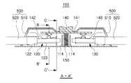
도 1을 참조하면, 광원모듈(10)은 복수의 발광소자(300)가 배치된 회로기판(400) 및 상기 회로기판(400)의 일면에 배치된 커넥터(100, 200)를 포함할 수 있다.
Referring to FIG. 1 , the
상기 회로기판(400)은 복수의 발광소자(300)와 전기적으로 연결되는 회로 배선을 구비하며, 일 방향으로 길게 연장된 판상의 바(bar) 형상을 가질 수 있다. 상기 회로기판(400)은 이러한 형상에 의하여 LCD 패널의 섀시 구조물에 종 또는 횡으로 정렬하여 백라이트 유닛으로 구성하기에 적합할 수 있다. 다만, 상기 회로기판(400)의 형상을 이에 한정되는 것은 아니며, 다양하게 변형할 수 있다.
The
또한, 회로기판(400)은 인쇄회로기판(PCB)의 일종으로 에폭시, 트리아진, 실리콘, 폴리이미드 등을 함유하는 유기 수지 소재 및 기타 유기 수지 소재로 형성될 수 있다. 또한, 회로기판(400)은 AlN, Al2O3 등의 세라믹 소재, 또는 금속 및 금속화합물을 소재로 하여 형성될 수 있으며, 예를 들어 메탈 PCB의 일종인 MCPCB가 포함될 수 있다.
In addition, the
상기 발광소자(300)는 전기 신호 인가 시 빛을 방출하는 소자라면 어느 것이나 사용될 수 있다. 일 실시예에서는 상기 발광소자(300)로 발광 다이오드(LED)가 이용될 수 있다. 이러한 발광 다이오드로는 성장기판 상에 반도체층을 에피택셜 성장시킨 반도체 발광소자를 이용할 수 있다.
As the
성장기판은 사파이어가 적용될 수 있으나, 이에 한정되는 것은 아니며, 예를 들어 스피넬, SiC, GaN, GaAs 등과 같은 성장용 기판을 이용할 수 있다. 구체적으로, 상기 발광소자(300)는 BN, SiC, ZnSe, GaN, InGaN, InAlGaN, AlGaN, BAlGaN, BInAlGaN 등으로 이루어질 수 있으며, Si 또는 Zn 등으로 도핑될 수 있다.
Sapphire may be applied to the growth substrate, but is not limited thereto, and for example, substrates for growth such as spinel, SiC, GaN, and GaAs may be used. Specifically, the
또한, 상기 발광소자(300)의 활성층은 AlxInyGa1-x-yN(0≤x≤1, 0≤y≤1, 0≤x+y≤1)로 이루어진 질화물 반도체로 구성될 수 있으며, 단일 또는 다중 양자 우물 구조로 이루어져 광출력을 향상시킬 수 있다.
In addition, the active layer of the
이때, 상기 발광소자(300)는 형광체 또는 양자점과 같은 파장변환물질에 의해 방출광이 백색광으로 변환될 수 있도록, 300 ~ 460nm의 단파장을 방출하는 질화물 반도체일 수 있다.
In this case, the
상기 발광소자(300)는 상기 회로기판(400)상에 복수 개 구비될 수 있으며, 복수 개의 발광소자(300)는 서로 전기적으로 연결될 수 있다. 예를 들어, 복수 개의 발광소자(300)는 서로 직렬로 연결되거나, 병렬로 연결되도록 구성될 수 있다. 또한, 직병렬로 연결되도록 구성될 수도 있다.
A plurality of light emitting
상기 회로기판(400)이 바(bar) 형상일 경우, 복수의 발광소자(300)는 회로기판(400)의 길이 방향(d1)을 따라 등간격으로 배열될 수 있다. 또한, 상기 발광소자(300)는 회로기판(400)의 폭(d2)을 반분하는 위치에 배치될 수 있다. 발광소자(300)는 칩 상태로 회로기판(400) 상에 실장될 수 있으며(소위, COB 구조), 패키지화되어 실장될 수도 있다.
When the
구체적으로, 일 실시예의 경우, 도 1에 도시된 바와 같이, 총 24개의 발광소자(300)가 바 형상의 회로기판(400)의 길이 방향(d1)으로 배열될 수 있다. 이때, 24개의 발광소자(300)는 8개의 단위로 발광소자 스트링(S1 ~ S3)을 이룰 수 있다. 각 발광소자 스트링(S1 ~ S3)은 서로 병렬을 이루도록 배치될 수 있으며, 각 발광소자 스트링(S1 ~ S3)을 이루는 8개의 발광소자(300)는 서로 직렬을 이루도록 배치될 수 있다. 다만, 발광소자(300)의 개수와 배치는 이에 한정되는 것은 아니며, 다양하게 변형될 수 있다.
Specifically, in the case of one embodiment, as shown in FIG. 1 , a total of 24 light emitting
상기 커넥터(100, 200)는 상기 복수의 발광소자(300)에 전원을 인가하기 위한 구성으로, 상기 회로기판(400)의 일면에 적어도 한 쌍이 구비될 수 있다. 일 실시예의 경우, 발광소자(300)가 실장된 면의 일 영역에 복수의 발광소자(300)를 기준으로, 회로기판(400)의 일측에만 배치될 수 있다.
The
상기 커넥터(100, 200)의 양단에는, 전원을 인가하기 위한 와이어가 각각 삽입되어 고정되는 제1 접속부(120, 220)와 제2 접속부(130, 230)가 각각 배치될 수 있다. 상기 제1 접속부(120, 220)와 제2 접속부(130, 230)는 상기 커넥터(100, 200)의 양단에 각각 서로 반대 방향을 향하여 배치되므로, 상기 제1 접속부(120, 220)와 제2 접속부(130, 230)에 삽입되는 각각의 와이어는 서로 마주보는 방향으로 삽입될 수 있다.
At both ends of the
일 실시예의 커넥터(100, 200)가 채용된 광원모듈(10)은 기존의 커넥터가 채용된 광원모듈에 비하여, 제조비용이 절감되고, 제조시간이 단축되는 효과가 있다. 이에 대하여 설명한다.
The
일 실시예의 광원모듈은 다양한 분야에 적용될 수 있으나, LCD 패널의 백라이트(back light)에 적용된 경우를 예를 들어 설명한다. 백라이트는 LCD 패널에 균일한 빛을 비출 수 있어야 한다. 따라서, 좀더 균일하게 빛을 비추기 위해, LCD 패널의 섀시 구조물에 더 많은 개수의 광원모듈을 배치할 필요성이 있었다.
Although the light source module of one embodiment can be applied to various fields, a case in which it is applied to a back light of an LCD panel will be described as an example. The backlight must be able to shine a uniform light on the LCD panel. Therefore, in order to illuminate the light more uniformly, there is a need to arrange a larger number of light source modules on the chassis structure of the LCD panel.
기존에는 와이어를 연결하는 제1 및 제2 접속부가 커넥터의 일단에 같은 방향을 향하도록 배치된, 소위, 2핀 커넥터를 사용하여 광원모듈을 구성하였다. 이러한 2핀 커넥터는, 제1 및 제2 접속부가 같은 방향을 향하여 서로 평행하게 배치되므로, 커넥터의 폭이 2개의 와이어를 삽입할 수 있을 정도가 되어야만 하였다.
In the past, a light source module was configured using a so-called 2-pin connector, in which first and second connectors for connecting wires are disposed to face the same direction at one end of the connector. In this 2-pin connector, since the first and second connectors face the same direction and are disposed parallel to each other, the width of the connector has to be such that two wires can be inserted.
따라서, 2핀 커넥터를 실장하기 위해서는 폭이 넓은 회로기판을 사용해야만 하는 문제점이 있었다. 이와 같은 폭이 넓은 회로기판은 제조비용을 증가시키는 문제점이 있었으며, LCD 패널의 섀시 구조물에 더 많은 개수의 광원모듈을 배치하는 데에 장애가 되었다.
Therefore, in order to mount the 2-pin connector, there was a problem in that a wide circuit board had to be used. Such a wide circuit board has a problem of increasing manufacturing cost, and has become an obstacle in arranging a larger number of light source modules in a chassis structure of an LCD panel.
이러한 문제점을 해소하고자, 상대적으로 폭이 좁은 1핀 커넥터를 사용하기도 하였다. 그러나, 1핀 커넥터는 접속부가 1개만 배치된 커넥터이므로, 2핀 커넥터를 사용하는 경우에 비해, 2배의 커넥터를 실장해야 하였다. 따라서, 제조시간이 증가하는 문제점이 발생하였다. 아울러, 커넥터의 개수가 증가하여 제조비용이 증가하는 문제점이 발생하였다.
In order to solve this problem, a relatively narrow 1-pin connector was used. However, since the 1-pin connector is a connector in which only one connecting part is disposed, twice as many connectors have to be mounted as compared to the case where a 2-pin connector is used. Therefore, a problem in that the manufacturing time increases has occurred. In addition, as the number of connectors increases, manufacturing costs increase.
이러한 문제점들을 해소하기 위해, 본 실시예는 와이어를 삽입하는 제1 접속부(120, 220)와 제2 접속부(130, 230)가 동일선상에서 서로 반대 방향을 향하여 배치된 구조를 가진 커넥터(100, 200)를 채용하였다.
In order to solve these problems, the present embodiment is a connector (100, 200) having a structure in which the first connection portion (120, 220) and the second connection portion (130, 230) for inserting the wire are disposed in opposite directions on the same line. ) was adopted.
따라서, 상기 커넥터(100)는 제1 및 제2 접속부가 커넥터의 일단에 같은 방향을 향하도록 구비된, 기존의 2핀 커넥터를 사용하는 경우에 비해, 커넥터의 폭을 절반 이하로 좁게 형성할 수 있다. 그러므로, 커넥터를 실장하기 위한 면적도 절반 이하로 감소되는 장점이 있다. 따라서, 기존에 비해 더 좁은 폭(d2)의 회로기판을 사용할 수 있으므로, 제조비용이 감소되는 효과가 있다.Therefore, in the
또한, 제1 접속부(120, 220)와 제2 접속부(130, 230)가 커넥터(100, 200)의 양단에 서로 반대방향으로 배치되므로, 와이어를 연결하는 제1 및 제2 접속부가 커넥터의 일단에 같은 방향을 향하도록 배치된 기존의 2핀 커넥터에 비하여, 제1 및 제2 접속부에 삽입되는 와이어 사이의 단락이 근본적으로 방지되는 장점이 있다.In addition, since the
아울러, 1핀 커넥터를 사용하는 경우에 비해, 필요한 커넥터의 수가 절반으로 감소하므로 제조비용이 감소되며, 커넥터를 실장하는 데에 소요되는 시간이 감소되는 효과가 있다.
In addition, compared to the case of using a 1-pin connector, since the number of necessary connectors is reduced by half, manufacturing costs are reduced and the time required to mount the connectors is reduced.
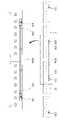
도 2 내지 도 6(b)를 참조하여, 상기 커넥터(100)에 대해 자세하게 설명한다. 도 2은 도 1의 커넥터의 사시도이고, 도 3은 도 2의 커넥터의 분해사시도이다. 도 4는 도 2의 커넥터에 와이어가 삽입된 모습을 나타낸 단면도이며, 도 5(a) 내지 도 6(b)는 누름 버튼을 눌러 와이어의 접속이 해제되는 모습을 나타낸 도면이다.
Referring to FIGS. 2 to 6(b), the
도 2를 참조하면, 상기 커넥터(100)는 와이어가 접속되는 제1 및 제2 접속부(120, 130), 상기 제1 및 제2 접속부(120, 130)를 덮는 하우징(110) 및 상기 제1 및 제2 접속부(120, 130)의 접속을 해제하는 누름 버튼(140)을 포함할 수 있다.
Referring to FIG. 2 , the
도 3을 참조하면, 상기 제1 및 제2 접속부(120, 130)는 솔더링부(121, 131), 커버링부(122, 132), 체결부(123, 133) 및 체결 해제부(124, 134)를 포함할 수 있다. 상기 제1 및 제2 접속부(120, 130)는 서로 반대 방향, 즉, 커넥터(100)를 회로기판(400)에 실장하면 제1 및 제2 접속부(120, 130)가 회로기판(400)의 양단을 향하도록 배치될 수 있다. 상기 제1 및 제2 접속부(120, 130)는 전기적 단락이 발생하지 않도록 서로 이격되어 배치될 수 있다. 또한, 상기 제1 및 제2 접속부(120, 130)는 후술할 누름 버튼(140)을 기준으로 서로 대칭되도록 배치될 수도 있다.
Referring to FIG. 3 , the first and
또한, 상기 제1 및 제2 접속부(120, 130)의 사이를 전기적으로 분리하기 위한 절연체가 더 배치될 수도 있다. 일 실시예는 절연체로서 하우징(110)의 일 영역에 절연격벽(114)을 형성할 수 있다(도 4 참조).
In addition, an insulator for electrically separating the first and
상기 제1 접속부(120)와 제2 접속부(130)는 동일한 구성이므로, 세부구조와 관련하여, 반복되는 설명을 방지하기 위해 제1 접속부(120)에 대해서만 설명한다.
Since the
솔더링부(121)는 상기 회로기판(400)에 상기 커넥터(100)를 실장할 때에 솔더링되어 부착되는 부분으로, 솔더링이 용이하도록 전체적으로 평평한 판 형태로 형성될 수 있다.
The
상기 커버링부(122)는 상기 솔더링부(121)의 상면과 교차하는 방향을 따라 연장될 수 있다. 상기 커버링부(122)는 상부의 일부 영역이 각각 절곡되어 상기 솔더링부(121)의 일단방향에서 삽입되는 와이어를 감싸도록 한 쌍으로 구성될 수 있다. 따라서, 각각의 커버링부(122)는 솔더링부(121)로부터 수직 상방으로 연장되되, 커버링부(122)의 수직 연장부분의 외측에는 하우징(110)의 측면과 결합이 견고히 이루어지도록 하우징(110)의 측면 내측이 걸리는 걸림턱(122a)이 각각 외측으로 돌출 형성된다.The covering
상기 체결부(123)는 각 커버링부(122)로부터 연장되어 한쌍으로 구비되되, 상기 커버링부(122)의 일단에 가까워질수록 서로 좁아지는 폭을 가지도록 구성될 수 있다. 상기 체결부(123)는 상기 커버링부(122)의 일단에 인접한 영역에서 삽입된 와이어와 결합하면서 체결될 수 있다.
The
체결부(123)는, 커버링부(122)로부터 솔더링부(121)의 타단 방향으로 각각 연장되되 서로 마주보는 방향의 반대방향으로 절곡된 제1 연장부분(123a)과, 제1 연장부분(123a)으로부터 솔더링부(121)의 타단 방향으로 각각 연장되되 서로 평행하게 연장되는 제2 연장부분(123b), 및 제2 연장부분(123b)으로부터 솔더링부(121)의 타단 방향으로 각각 연장되되 서로 마주보는 방향으로 경사지게 연장되며 단부 사이에 와이어가 끼워져 체결되는 제3 연장부분(123c)을 포함한다. 이러한 벤딩구조에 의해 상기 체결부(123)는 자체에 탄성력을 갖는다.
The
체결 해제부(124)는 각 체결부(123)의 상부에 각각 배치되며, 상기 누름 버튼(140)의 일부 영역이 삽입되는 틈을 가지도록 서로 대향되게 배치된다. 특히, 제2 연장부분(123b)의 상부로부터 연장될 수 있다.
The
상기 체결 해제부(124)는 와이어의 체결 해제 시에, 누름 버튼(140)의 제1 및 제2 끼움부(142, 143)가 틈에 삽입되어, 상기 체결부(123)를 벌어지도록 함으로써 와이어의 체결이 해제되도록 구성될 수 있다.
When the wire is disconnected, the
상기 하우징(110)은 절연성 수지를 몰딩하여 형성할 수 있다. 상기 하우징(110)은 측면과 상면으로 이루어지며, 상면에는 누름 버튼(140)을 상방으로 노출시키는 누름 버튼 노출홀(113)이 형성되고, 양단부에는 와이어가 삽입되는 와이어 삽입홀(111, 112)이 각각 형성될 수 있다.
The
상기 하우징(110)은 제1 및 제2 접속부(120, 130)을 인서트하고 인서트 사출 몰딩(Insert Injection Molding)함으로써 형성될 수 있다. 또한, 상기 하우징(110)은 이중 사출 몰딩(double Injection Molding)하여 형성할 수도 있으나, 이에 한정하는 것은 아니며, 별도로 제조하여 상기 제1 및 제2 접속부(120, 130)에 결합하는 것도 가능하다. 상기 하우징(110)의 내부에는 상기 제1 및 제2 접속부(120, 130)가 서로 전기적으로 분리되도록 절연 격벽(114)을 배치할 수도 있다.
The
상기 누름 버튼(140)은 상기 하우징(110)의 내부 공간에 수납되되, 상기 제1 및 제2 접속부(120, 130) 상에 배치되어, 누르는 동작과 같이 외부에게 가해지는 힘에 의해 상기 제1 및 제2 접속부(120, 130)의 접속을 해제할 수 있다. 상기 누름 버튼(140)은 걸림부(141) 및 제1 및 제2 끼움부(142, 143)를 포함할 수 있다.
The
상기 누름 버튼(140)의 상부는 누름 버튼 노출홀(113)을 통해 노출되도록 누름 버튼 노출홀(113)보다 작은 크기로 배치되어, 상기 누름 버튼(140)의 상부가 상기 누름 버튼 노출홀(133)을 통과하여 돌출되도록 형성될 수 있다.
The upper portion of the
상기 걸림부(141)는, 상기 누름 버튼(140)이 상기 누름 버튼 노출홀(113)을 통해 분리되지 않도록, 전체적으로 상기 누름 버튼 노출홀(113)보다 큰 크기로 형성될 수 있다.
The hanging
상기 걸림부(141)의 하부에는 제1 및 제2 끼움부(142, 143)가 배치될 수 있다. 상기 제1 및 제2 끼움부(142, 143)는 상기 체결 해제부(124, 134) 상에 각각 위치하도록 배치되어, 상기 누름 버튼(140)에 외부의 힘이 가해지면, 각 체결 해제부(124, 134)의 사이에 끼워지면서 상기 체결부(123, 133)가 벌어져 와이어가 제거될 수 있도록 구성될 수 있다. 따라서, 누름 버튼(140)을 누름으로써, 체결부(123, 133)에 끼워진 각각의 와이어를 한번에 제거할 수 있다.First and second
본 실시예는 1개의 누름 버튼(140)의 하부에 제1 및 제2 끼움부(142, 143)가 배치된 경우를 예를 들어 설명하였으나, 제1 및 제2 끼움부(142, 143) 각각에 누름 버튼이 배치되게 변형하는 것도 가능하다.
Although the present embodiment has been described as an example in which the first and second
또한, 상기 걸림부(141)의 하부에는 스프링(150)과 같은 탄성부재가 배치되어, 누름 버튼(140)을 누르던 외부의 힘을 제거하면 누름 버튼(140)이 원상태로 상승하도록 구성될 수 있다.
In addition, an elastic member such as a
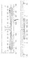
도 4 내지 도 6(b)를 참조하여, 커넥터(100)에 삽입되어 있던 와이어(500)의 체결을 해제시키는 과정을 설명한다.
Referring to FIGS. 4 to 6( b ), a process of releasing the fastening of the
도 4는, 제1 및 제2 접속부(120, 130)에 각각 와이어(500)가 삽입되어, 커버링부(122)에 와이어(500)의 피복부(520)가 끼워지고, 체결부(123)에는 전선부(510)가 체결된 상태를 보여준다. 도 5(a)는 도 4의 B-B'의 단면을 도시한 것이며, 도 5(b)는 도 4의 C-C'의 단면을 도시한 것이다.
4 shows that the
도 5(a)을 참조하면, 누름 버튼(140)을 누르기 전에는, 제1 끼움부(142)는 체결 해제부(124)의 상부와 이격되어 있다. 또한, 도 5(b)와 같이, 체결부(123)의 제3 연장 부분(123c)이 전선부(510)와 접속되어 있다.
Referring to FIG. 5 ( a ) , before pressing the
도 6(a)와 같이 누름 버튼(140)을 가압하면, 제1 끼움부(142)가 체결 해제부(124)의 사이에 끼워지게 된다. 따라서, 도 6(b)와 같이, 체결부(123)의 제3 연장 부분(123c)이 전선부(510)와 이격되어 체결이 해제된다.
When the
와이어(500)의 체결이 해제되어 와이어(500)를 빼고 누름 버튼(140)을 누르고 있던 힘을 해제하면, 누름 버튼(140)을 지지하는 스프링(150)이 가지는 탄성력에 의해 누름 버튼(140)은 원상태로 복귀된다.
When the fastening of the
상기 커넥터(100)는 도 7에 도시된 바와 같이, 변형될 수 있다.As shown in FIG. 7 , the
도 7은 변형예의 커넥터(100a)의 측면도이다. 변형예(100a)는, 솔더링부(121, 131)가 각각 하우징(110)의 하부로 노출된 연장부분(121a, 131a)과, 연장부분(121a, 131a)에서 와이어가 삽입되는 방향으로 절곡된 평탄부(121b, 131b)로 구성될 수 있다.
Fig. 7 is a side view of a modified
변형예의 커넥터(100a)는 솔더링부(121, 131)의 평탄부(121b, 131b)가 하우징(110)으로부터 이격되도록 배치된 특징이 있다. 이와 같이 구성하면, 후술하는 바와 같이, 광원모듈을 섀시 구조물에 실장할 때에, 와이어를 발광소자가 실장된 면의 타면에서 삽입할 수 있는 장점이 있다.
The
상기 광원모듈(10)은 복수개를 직렬 또는 병렬연결할 수 있다. 도 8 및 도 9을 참조하여, 이에 대해 설명한다.A plurality of the
도 8는 복수의 광원모듈을 직렬연결한 일 예이며, 도 9는 복수의 광원모듈을 병렬연결한 일 예이다.
8 is an example of connecting a plurality of light source modules in series, and FIG. 9 is an example of connecting a plurality of light source modules in parallel.
도 8에 도시된 바와 같이, 어느 하나의 광원모듈(11)과 인접한 광원모듈(12)을 하나의 와이어(500a)로 연결함으로써, 두 광원모듈(11, 12)을 서로 직렬연결할 수 있다. 구체적으로, 어느 하나의 광원모듈(11)의 제2 접속부(230)와 인접한 광원모듈(12)의 제1 접속부(120)를 와이어(500a)로 연결함으로써, 두 광원모듈(11, 12)을 서로 직렬연결할 수 있다.
As shown in FIG. 8 , two
도 9에 도시된 바와 같이, 어느 하나의 광원모듈(11)과 인접한 광원모듈(12)을 한 쌍의 와이어(500b, 500c)로 연결함으로써, 두 광원모듈(11, 12)을 서로 병렬연결할 수 있다. 구체적으로, 어느 하나의 광원모듈(11)의 제1 접속부(220)와 인접한 광원모듈(12)의 제1 접속부(120)를 와이어(500b)로 연결하고, 어느 하나의 광원모듈(11)의 제2 접속부(230)와 인접한 광원모듈(12)의 제2 접속부(130)를 와이어(500c)로 연결함으로써, 두 광원모듈(11, 12)을 서로 병렬연결할 수 있다.
As shown in FIG. 9, by connecting one
따라서, 필요에 따라, 실시예의 복수의 광원모듈(11, 12) 사이의 와이어 연결만 변경하면, 복수의 광원모듈(11, 12)의 회로 연결을 손쉽게 변경할 수 있다.
Therefore, if necessary, by changing only the wire connection between the plurality of
도 10은 복수의 광원모듈(11 ~ 14)로 광원모듈 어레이(1000)를 구성한 예이다.10 is an example of configuring the light
일 실시예의 광원모듈 어레이(1000)는 4개의 광원모듈(11 ~ 14)이 LCD 패널의 섀시 구조물(600)에 2행 2열로 배치된 것을 도시하고 있다. 각각의 광원모듈(11 ~14)은 서로 직렬 연결되는 경우를 예를 들어 설명하였으나, 앞서 설명한 바와 같이, 복수의 광원모듈(11 ~ 14)의 회로 연결은 와이어(500)의 배선을 변경함으로써, 손쉽게 바꿀 수 있다.
The light
상기 광원모듈 어레이(1000)는 섀시 구조물(600)에 광원모듈 어레이(11 ~ 14)를 배치한 후, 커넥터(100, 200)에 와이어(500)를 접속함으로 구성할 수 있다.
The light
도 11(a) 및 도 11(b)는 광원모듈 어레이의 다른 실시예이다. 본 실시예는 일 실시예와 비교하여, 커넥터(100a, 200a)의 구성이 상이하다. 본 실시예에 채용되는 커넥터(100a, 200a)는 도 7에 도시된 커넥터이다. 앞서 설명한 일 실시예와 다른 커넥터를 채용함으로써, 광원모듈 어레이(2000)의 와이어(500) 배선 방법이 달라지므로, 이를 중점으로 설명한다.
11(a) and 11(b) are other embodiments of a light source module array. Compared to the previous embodiment, the configuration of the
도 11(b)에 도시된 바와 같이, 본 실시예의 광원모듈 어레이(2000)에는 회로기판(400) 및 섀시 구조물(600a)을 각각 관통하는 결합홀(410a, 610a)이 구비된다. 이 결합홀(410a, 610a)은, 커넥터(100a)의 하우징(110)이 삽입될 수 있을 정도의 크기로 형성되되, 평탄부(121b, 131b)까지는 삽입되지 않을 정도의 크기로 형성될 수 있다. 따라서, 커넥터(100a)의 평탄부(121b, 131b)가 회로기판(400)의 소정 영역과 맞닿도록 배치될 수 있다.
As shown in FIG. 11(b), the light
따라서, 회로기판(400)과 평탄부(121b, 131b)를 솔더링(700)하여 접속시킬 수 있다. 상기 하우징(110)은 결합홀(410a, 610a)을 관통하여 돌출되므로, 와이어(500)를 섀시 구조물(600a)의 하부에서 결합시킬 수 있는 장점이 있다.
Therefore, the
도 12 및 도 13은 도 1의 광원모듈에 채용된 발광소자(300)의 예를 나타낸다.
12 and 13 show examples of the
도 12를 참조하면, 광원모듈(3100)은, 회로 기판(3110) 및 회로 기판(3110) 상에 실장된 복수의 백색광 발광장치들(3100a)의 배열을 포함할 수 있다. 회로 기판(3110) 상면에는 백색광 발광장치(3100a)와 접속되는 도전 패턴이 형성될 수 있다.
Referring to FIG. 12 , the
각각의 백색광 발광장치(3100a)는, 청색광을 방출하는 발광소자(3130)가 회로 기판(3110)에 COB(Chip On Board) 방식으로 직접 실장되는 구조를 가질 수 있다. 각각의 백색광 발광장치(3100a)는 별도의 반사벽을 갖지 않으며, 파장변환부(3150a)가 렌즈 기능을 갖는 반구형상으로 구비되어 넓은 지향각을 나타낼 수 있다. 이러한 넓은 지향각은, LCD 디스플레이의 두께 또는 폭을 감소시키는데 기여할 수 있다.
Each white
도 13을 참조하면, 광원모듈(3200)은, 회로 기판(3110) 및 회로 기판(3110) 상에 실장된 복수의 백색광 발광장치들(3100b)의 배열을 포함할 수 있다. 각각의 백색광 발광장치(3100b)는 패키지 본체(3125)의 반사컵 내에 실장된 청색광을 방출하는 발광소자(3130) 및 이를 봉지하는 파장변환부(3150b)를 구비할 수 있다.
Referring to FIG. 13 , the
상기 파장변환부(3150a, 3150b)는 수지(3152)에 형광체 및/또는 양자점과 같은 파장변환물질(3154, 3156)이 함유된 형태로 형성될 수 있다.
The
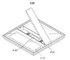
도 15를 참조하면, 평판 조명 장치(4100)는 광원모듈(4110), 전원공급장치(4120) 및 하우징(4030)을 포함할 수 있다. 본 발명의 예시적 실시예에 따라, 광원모듈(4110)은, 앞서 설명한 도 1의 광원모듈(10)을 광원으로 포함할 수 있고, 전원공급장치(4120)는 광원모듈(4110)의 구동부를 포함할 수 있다.
Referring to FIG. 15 , a
광원모듈(4110)은 복수의 발광소자를 포함할 수 있고, 전체적으로 평면 현상을 이루도록 형성될 수 있다. 본 발명의 예시적 실시예에 따라, 발광소자 어레이는 발광소자 및 발광소자의 구동정보를 저장하는 컨트롤러를 포함할 수 있다.
The
전원공급장치(4120)는 광원모듈(4110)에 전원을 공급하도록 구성될 수 있다. 하우징(4130)은 광원모듈(4110) 및 전원공급장치(4120)가 내부에 수용되도록 수용 공간이 형성될 수 있고, 일측면에 개방된 육면체 형상으로 형성되나 이에 한정되는 것은 아니다. 광원모듈(4110)은 하우징(4130)의 개방된 일측면으로 빛을 발광하도록 배치될 수 있다.
The
본 발명은 상술한 실시예 및 첨부된 도면에 의해 한정되는 것이 아니며 첨부된 청구범위에 의해 한정하고자 한다. 따라서, 청구범위에 기재된 본 발명의 기술적 사상을 벗어나지 않는 범위 내에서 당 기술분야의 통상의 지식을 가진 자에 의해 다양한 형태의 치환, 변형 및 변경이 가능할 것이며, 이 또한 본 발명의 범위에 속한다고 할 것이다.
The present invention is not limited by the above-described embodiments and accompanying drawings, but is intended to be limited by the appended claims. Therefore, various forms of substitution, modification, and change will be possible by those skilled in the art within the scope of the technical spirit of the present invention described in the claims, which also falls within the scope of the present invention. something to do.
10: 광원모듈
100, 200: 커넥터
110: 하우징
111, 112: 와이어 삽입홀
113: 누름 버튼 노출홀
114: 절연 격벽
120: 제1 접속부
121, 131: 솔더링부
122, 132: 커버링부
123, 133: 체결부
124, 134: 체결 해제부
130: 제2 접속부
140: 누름 버튼
141: 걸림부
142: 제1 끼움부
143: 제2 끼움부
150: 스프링
300: 발광소자
400: 회로기판
500: 와이어
510: 전선부
520: 피복부10: light source module
100, 200: connector
110: housing
111, 112: wire insertion hole
113: push button exposure hole
114: insulating bulkhead
120: first connection part
121, 131: soldering part
122, 132: covering part
123, 133: fastening part
124, 134: coupling release unit
130: second connection part
140: push button
141: hanging part
142: first fitting part
143: second fitting part
150: spring
300: light emitting element
400: circuit board
500: wire
510: wire part
520: covering part
Claims (20)
Translated fromKorean상기 회로기판의 일면에 실장되며, 상기 복수의 발광소자의 일측에 상기 제1 방향으로 각각 배치되고 상기 복수의 발광소자와 전기적으로 연결되는 제1 및 제2 커넥터;를 포함하며,
상기 제1 및 제2 커넥터 각각은,
삽입된 와이어와 결합되며, 서로 반대 방향을 향하여 배치되는 제1 및 제2 접속부;
상기 제1 및 제2 접속부를 덮는 하우징; 및
상기 제1 및 제2 접속부 상에 배치되며, 외부에서 가해지는 힘에 의해 상기 제1 및 제2 접속부와 상기 삽입된 와이어의 결합을 해제하는 누름 버튼;을 포함하며,
상기 제1 및 제2 접속부는 각각,
상기 회로기판에 솔더링되는 판 형태의 솔더링부;
상기 솔더링부의 상면과 교차하는 방향을 따라 연장되며, 상부에서 적어도 일부 영역이 절곡되어 상기 삽입된 와이어를 감싸는 커버링부;
상기 커버링부로부터 연장되어 상기 커버링부의 일단에 가까워질수록 좁아지는 폭을 가지며, 상기 커버링부의 일단에 인접한 영역에서 상기 삽입된 와이어와 결합하는 체결부; 및
상기 체결부의 상부에 배치되어 상기 누름 버튼의 일부 영역이 삽입되는 틈을 가지며, 상기 누름 버튼의 일부 영역이 상기 틈에 삽입될 때 상기 삽입된 와이어와 상기 체결부의 결합을 해제하는 체결 해제부;를 포함하는 것을 특징으로 하는 광원모듈.
a circuit board on which a plurality of light emitting devices are disposed along a first direction; and
First and second connectors mounted on one surface of the circuit board, disposed on one side of the plurality of light emitting elements in the first direction, and electrically connected to the plurality of light emitting elements,
Each of the first and second connectors,
first and second connectors coupled to the inserted wire and disposed in opposite directions;
a housing covering the first and second connectors; and
A push button disposed on the first and second connection parts and releasing the coupling between the first and second connection parts and the inserted wire by an externally applied force,
The first and second connecting parts, respectively,
a soldering unit in the form of a plate that is soldered to the circuit board;
a covering part extending along a direction crossing the upper surface of the soldering part and having at least a partial region bent at the top thereof to surround the inserted wire;
a fastening portion extending from the covering portion and having a narrower width as it approaches one end of the covering portion, and coupled to the inserted wire in an area adjacent to one end of the covering portion; and
a coupling release unit disposed above the fastening unit, having a gap into which a partial area of the push button is inserted, and disengaging the inserted wire from the fastening unit when a partial area of the push button is inserted into the gap; A light source module comprising:
상기 회로기판은 바(bar)형인 것을 특징으로 하는 광원모듈.
According to claim 3,
The light source module, characterized in that the circuit board is a bar (bar) type.
상기 제1 및 제2 접속부는 각각 상기 회로기판의 양단을 향하도록 배치된 것을 특징으로 하는 광원모듈.
According to claim 3,
The light source module, characterized in that the first and second connectors are disposed to face both ends of the circuit board, respectively.
상기 회로기판의 일면에 실장되며, 상기 복수의 발광소자의 일측에 상기 제1 방향으로 각각 배치되고 상기 복수의 발광소자와 전기적으로 연결되는 제1 및 제2 커넥터;를 갖는 복수의 광원모듈을 포함하며,
상기 제1 및 제2 커넥터 각각은,
삽입된 와이어와 기계적으로 결합되며, 상기 회로기판의 양단을 향하여 각각 배치되는 제1 및 제2 접속부와, 상기 제1 및 제2 접속부 상에 배치되며, 외부에서 가해지는 힘에 의해 상기 제1 및 제2 접속부와 상기 삽입된 와이어의 결합을 해제하는 누름 버튼을 포함하고,
상기 제1 및 제2 접속부는 각각,
상기 회로기판에 솔더링되는 판 형태의 솔더링부;
상기 솔더링부의 상면과 교차하는 방향을 따라 연장되며, 상부에서 적어도 일부 영역이 절곡되어 상기 삽입된 와이어를 감싸는 커버링부;
상기 커버링부로부터 연장되어 상기 커버링부의 일단에 가까워질수록 좁아지는 폭을 가지며, 상기 커버링부의 일단에 인접한 영역에서 상기 삽입된 와이어와 결합하는 체결부; 및
상기 체결부의 상부에 배치되어 상기 누름 버튼의 일부 영역이 삽입되는 틈을 가지며, 상기 누름 버튼의 일부 영역이 상기 틈에 삽입될 때 상기 삽입된 와이어와 상기 체결부의 결합을 해제하는 체결 해제부;를 포함하고
상기 삽입된 와이어는 상기 복수의 광원모듈 중 어느 하나의 상기 제2 커넥터를 인접한 다른 상기 광원모듈의 상기 제1 커넥터와 전기적으로 연결하는 것을 특징으로 하는 광원모듈 어레이.
a circuit board on which a plurality of light emitting devices are disposed along a first direction; and
A plurality of light source modules having first and second connectors mounted on one surface of the circuit board, disposed on one side of the plurality of light emitting elements in the first direction, and electrically connected to the plurality of light emitting elements. and
Each of the first and second connectors,
First and second connectors that are mechanically coupled to the inserted wire and disposed toward both ends of the circuit board, and disposed on the first and second connectors, the first and second connectors are disposed on the first and second connectors by force applied from the outside. And a push button for releasing the coupling between the second connection part and the inserted wire,
The first and second connecting parts, respectively,
a soldering unit in the form of a plate that is soldered to the circuit board;
a covering part extending along a direction crossing the upper surface of the soldering part and having at least a partial region bent at the top thereof to surround the inserted wire;
a fastening portion extending from the covering portion and having a narrower width as it approaches one end of the covering portion, and coupled to the inserted wire in an area adjacent to one end of the covering portion; and
a coupling release unit disposed above the fastening unit, having a gap into which a partial area of the push button is inserted, and disengaging the inserted wire from the fastening unit when a partial area of the push button is inserted into the gap; include
The inserted wire electrically connects the second connector of one of the plurality of light source modules to the first connector of another adjacent light source module.
상기 복수의 광원모듈은 서로 직렬 연결되는 것을 특징으로 하는 광원모듈 어레이.
According to claim 6,
The light source module array, characterized in that the plurality of light source modules are connected in series with each other.
상기 삽입된 와이어는 상기 복수의 광원모듈 중 어느 하나의 상기 제2 커넥터의 제2 접속부를, 인접한 다른 상기 광원모듈의 상기 제1 커넥터의 제1 접속부와 전기적으로 연결하는 것을 특징으로 하는 광원모듈 어레이.
According to claim 7,
The inserted wire electrically connects the second connection part of the second connector of one of the plurality of light source modules to the first connection part of the first connector of the adjacent other light source module. .
상기 복수의 광원모듈은 서로 병렬 연결되는 것을 특징으로 하는 광원모듈 어레이.
According to claim 6,
The light source module array, characterized in that the plurality of light source modules are connected in parallel with each other.
상기 삽입된 와이어는 상기 복수의 광원모듈 중 어느 하나의 상기 제2 커넥터의 제1 접속부를 인접한 다른 상기 광원모듈의 상기 제1 커넥터의 제1 접속부와 전기적으로 연결하며,
상기 어느 하나의 광원모듈의 상기 제2 커넥터의 제2 접속부를 상기 인접한 다른 광원모듈의 상기 제1 커넥터의 제2 접속부를 전기적으로 연결하는 것을 특징으로 하는 광원모듈 어레이.According to claim 9,
The inserted wire electrically connects the first connection part of the second connector of one of the plurality of light source modules to the first connection part of the first connector of the adjacent other light source module,
A light source module array, characterized in that electrically connecting the second connection part of the second connector of one light source module to the second connection part of the first connector of the other adjacent light source module.
Priority Applications (4)
| Application Number | Priority Date | Filing Date | Title |
|---|---|---|---|
| KR1020150116838AKR102476138B1 (en) | 2015-08-19 | 2015-08-19 | Connector, light source module and light source module array using the same |
| US15/150,960US9995960B2 (en) | 2015-08-19 | 2016-05-10 | Connector, light source module including the connector, and light source module array including the light source module |
| CN201610685600.5ACN106468838B (en) | 2015-08-19 | 2016-08-18 | Connector, light source module including the connector, and light source module array |
| US15/982,613US10216035B2 (en) | 2015-08-19 | 2018-05-17 | Connector, light source module including the connector, and light source module array including the light source module |
Applications Claiming Priority (1)
| Application Number | Priority Date | Filing Date | Title |
|---|---|---|---|
| KR1020150116838AKR102476138B1 (en) | 2015-08-19 | 2015-08-19 | Connector, light source module and light source module array using the same |
Publications (2)
| Publication Number | Publication Date |
|---|---|
| KR20170022171A KR20170022171A (en) | 2017-03-02 |
| KR102476138B1true KR102476138B1 (en) | 2022-12-14 |
Family
ID=58157181
Family Applications (1)
| Application Number | Title | Priority Date | Filing Date |
|---|---|---|---|
| KR1020150116838AActiveKR102476138B1 (en) | 2015-08-19 | 2015-08-19 | Connector, light source module and light source module array using the same |
Country Status (3)
| Country | Link |
|---|---|
| US (2) | US9995960B2 (en) |
| KR (1) | KR102476138B1 (en) |
| CN (1) | CN106468838B (en) |
Families Citing this family (2)
| Publication number | Priority date | Publication date | Assignee | Title |
|---|---|---|---|---|
| WO2018166292A1 (en)* | 2017-03-17 | 2018-09-20 | 欧普照明股份有限公司 | Illumination device |
| CN106989362A (en)* | 2017-03-17 | 2017-07-28 | 欧普照明股份有限公司 | Lighting device |
Citations (2)
| Publication number | Priority date | Publication date | Assignee | Title |
|---|---|---|---|---|
| KR101390960B1 (en)* | 2013-03-29 | 2014-05-02 | 몰렉스 인코포레이티드 | Poke in connector |
| KR102133889B1 (en) | 2013-06-28 | 2020-07-14 | 엘지이노텍 주식회사 | Circuit board and lighting device having the circuit board |
Family Cites Families (57)
| Publication number | Priority date | Publication date | Assignee | Title |
|---|---|---|---|---|
| DE1918193A1 (en)* | 1969-04-10 | 1970-10-15 | Merten Geb | Screwless connection terminal for electrical devices, especially installation devices |
| DE3514099C2 (en)* | 1985-04-16 | 1994-11-17 | Wago Verwaltungs Gmbh | Connection clamp for electrical conductors |
| DE4016770A1 (en)* | 1990-05-25 | 1991-11-28 | Guenter Trautmann | Cable connector for coarse and fine wires - relies on compression of wire between teeth of moulding and upper surface of depressed flat spring |
| CN1143394C (en) | 1996-08-27 | 2004-03-24 | 精工爱普生株式会社 | Peeling method, thin film device transfer method and thin film device |
| USRE38466E1 (en) | 1996-11-12 | 2004-03-16 | Seiko Epson Corporation | Manufacturing method of active matrix substrate, active matrix substrate and liquid crystal display device |
| JPH1197124A (en)* | 1997-09-22 | 1999-04-09 | Japan Aviation Electron Ind Ltd | High-speed transmission system and connector |
| US7208725B2 (en) | 1998-11-25 | 2007-04-24 | Rohm And Haas Electronic Materials Llc | Optoelectronic component with encapsulant |
| JP3906654B2 (en) | 2000-07-18 | 2007-04-18 | ソニー株式会社 | Semiconductor light emitting device and semiconductor light emitting device |
| ES1047528Y (en)* | 2000-11-03 | 2001-09-01 | Codina Maria Cristina Moret | BLOCK FOR QUICK EMBORNED TERMINALS |
| US6660935B2 (en) | 2001-05-25 | 2003-12-09 | Gelcore Llc | LED extrusion light engine and connector therefor |
| US6818465B2 (en) | 2001-08-22 | 2004-11-16 | Sony Corporation | Nitride semiconductor element and production method for nitride semiconductor element |
| JP2003218034A (en) | 2002-01-17 | 2003-07-31 | Sony Corp | Selective growth method, semiconductor light emitting device and method of manufacturing the same |
| JP3815335B2 (en) | 2002-01-18 | 2006-08-30 | ソニー株式会社 | Semiconductor light emitting device and manufacturing method thereof |
| KR100803181B1 (en)* | 2002-04-19 | 2008-02-14 | 삼성전자주식회사 | Backlight assembly |
| KR100499129B1 (en) | 2002-09-02 | 2005-07-04 | 삼성전기주식회사 | Light emitting laser diode and fabricatin method thereof |
| US7002182B2 (en) | 2002-09-06 | 2006-02-21 | Sony Corporation | Semiconductor light emitting device integral type semiconductor light emitting unit image display unit and illuminating unit |
| US20040092142A1 (en)* | 2002-11-07 | 2004-05-13 | Consolidated Manufacturing International, Llc | Clamping apparatus for connecting ground wire to grounding member |
| KR100714639B1 (en) | 2003-10-21 | 2007-05-07 | 삼성전기주식회사 | Light emitting element |
| JP4297825B2 (en) | 2003-11-04 | 2009-07-15 | モレックス インコーポレイテド | Cable connector |
| KR100506740B1 (en) | 2003-12-23 | 2005-08-08 | 삼성전기주식회사 | Nitride semiconductor light emitting device and method of manufacturing the same |
| KR100664985B1 (en) | 2004-10-26 | 2007-01-09 | 삼성전기주식회사 | Nitride-based semiconductor device |
| US7377669B2 (en) | 2005-03-28 | 2008-05-27 | U.S. Led, Ltd. | LED module and system of LED modules with integral branch connectors |
| KR100665222B1 (en) | 2005-07-26 | 2007-01-09 | 삼성전기주식회사 | LED package using diffusion material and manufacturing method thereof |
| KR100661614B1 (en) | 2005-10-07 | 2006-12-26 | 삼성전기주식회사 | Nitride-based semiconductor light emitting device and its manufacturing method |
| KR100723247B1 (en) | 2006-01-10 | 2007-05-29 | 삼성전기주식회사 | Chip coated LED package and manufacturing method thereof |
| KR100735325B1 (en) | 2006-04-17 | 2007-07-04 | 삼성전기주식회사 | Light emitting diode package and its manufacturing method |
| KR100788400B1 (en)* | 2006-09-06 | 2008-01-02 | 희성전자 주식회사 | Power connector and direct backlight unit |
| KR100930171B1 (en) | 2006-12-05 | 2009-12-07 | 삼성전기주식회사 | White light emitting device and white light source module using same |
| US7513793B2 (en)* | 2006-12-22 | 2009-04-07 | Tyco Electronics Corporation | Surface mount poke in connector |
| CN101578475B (en)* | 2007-01-22 | 2012-03-07 | 夏普株式会社 | Light source module and backlight light source |
| KR20080086105A (en) | 2007-03-21 | 2008-09-25 | 주식회사 옵토필 | LED module with connector structure |
| KR100855065B1 (en) | 2007-04-24 | 2008-08-29 | 삼성전기주식회사 | Light emitting diode package |
| KR100982980B1 (en) | 2007-05-15 | 2010-09-17 | 삼성엘이디 주식회사 | Surface light source device and LCD backlight unit having same |
| KR101164026B1 (en) | 2007-07-12 | 2012-07-18 | 삼성전자주식회사 | Nitride semiconductor light emitting device and fabrication method thereof |
| KR100891761B1 (en) | 2007-10-19 | 2009-04-07 | 삼성전기주식회사 | Semiconductor light emitting device, manufacturing method thereof and semiconductor light emitting device package using same |
| US7628640B2 (en)* | 2007-12-14 | 2009-12-08 | Actuant Corporation | Electrical connector for connection to multiple conductors |
| KR101332794B1 (en) | 2008-08-05 | 2013-11-25 | 삼성전자주식회사 | Light emitting device, light emitting system comprising the same, and fabricating method of the light emitting device and the light emitting system |
| KR20100024073A (en)* | 2008-08-25 | 2010-03-05 | 삼성전기주식회사 | Illumination apparatus |
| KR20100030470A (en) | 2008-09-10 | 2010-03-18 | 삼성전자주식회사 | Light emitting device and system providing white light with various color temperatures |
| KR101530876B1 (en) | 2008-09-16 | 2015-06-23 | 삼성전자 주식회사 | Light emitting device with increased light emitting amount, light emitting device including same, method of manufacturing light emitting device and light emitting device |
| US8008683B2 (en) | 2008-10-22 | 2011-08-30 | Samsung Led Co., Ltd. | Semiconductor light emitting device |
| KR101016112B1 (en) | 2008-11-04 | 2011-02-21 | 에프씨산업 주식회사 | LED lamps with connectors for multiple connections |
| KR100894258B1 (en) | 2008-11-24 | 2009-04-21 | 진영정보통신 주식회사 | LED lighting module |
| US8382322B2 (en) | 2008-12-08 | 2013-02-26 | Avx Corporation | Two part surface mount LED strip connector and LED assembly |
| JP5366688B2 (en)* | 2009-07-16 | 2013-12-11 | 日本航空電子工業株式会社 | Socket, substrate assembly, and apparatus including the same |
| KR20110073824A (en)* | 2009-12-24 | 2011-06-30 | 박광준 | Connector for LED module and LED module assembly including the same |
| DE102010014143B4 (en)* | 2010-04-07 | 2016-07-07 | Wago Verwaltungsgesellschaft Mbh | Actuation device for an electrical connection terminal |
| KR101744970B1 (en) | 2010-06-17 | 2017-06-08 | 엘지이노텍 주식회사 | Light emitting module and light unit using the same |
| JP5571539B2 (en)* | 2010-07-23 | 2014-08-13 | 京セラコネクタプロダクツ株式会社 | Connector and LED lighting apparatus using the connector |
| KR101295119B1 (en) | 2010-11-10 | 2013-08-12 | 삼성전자주식회사 | Light emitting module |
| JP5736262B2 (en) | 2011-07-14 | 2015-06-17 | モレックス インコーポレイテドMolex Incorporated | Multi-contact connector |
| DE102011056410B4 (en)* | 2011-12-14 | 2013-06-27 | Wago Verwaltungsgesellschaft Mbh | terminal |
| US9166327B2 (en)* | 2012-07-12 | 2015-10-20 | Vode Lighting Llc | Circuit board connector system |
| DE202013002763U1 (en)* | 2013-03-21 | 2013-05-27 | Liang-Chih Cheng | Screwless terminal block |
| JP5480990B1 (en)* | 2013-03-28 | 2014-04-23 | 日本航空電子工業株式会社 | Connector assembly |
| US20140299893A1 (en)* | 2013-04-05 | 2014-10-09 | Joint Tech Electronic Industrial Co., Ltd. | Conductive Connector For Use With Circuit Board, and LED Module Having the Same |
| CN203477986U (en)* | 2013-08-26 | 2014-03-12 | 南京中电熊猫液晶显示科技有限公司 | LED backlight module group |
- 2015
- 2015-08-19KRKR1020150116838Apatent/KR102476138B1/enactiveActive
- 2016
- 2016-05-10USUS15/150,960patent/US9995960B2/enactiveActive
- 2016-08-18CNCN201610685600.5Apatent/CN106468838B/enactiveActive
- 2018
- 2018-05-17USUS15/982,613patent/US10216035B2/enactiveActive
Patent Citations (2)
| Publication number | Priority date | Publication date | Assignee | Title |
|---|---|---|---|---|
| KR101390960B1 (en)* | 2013-03-29 | 2014-05-02 | 몰렉스 인코포레이티드 | Poke in connector |
| KR102133889B1 (en) | 2013-06-28 | 2020-07-14 | 엘지이노텍 주식회사 | Circuit board and lighting device having the circuit board |
Also Published As
| Publication number | Publication date |
|---|---|
| US10216035B2 (en) | 2019-02-26 |
| US9995960B2 (en) | 2018-06-12 |
| CN106468838B (en) | 2021-02-26 |
| KR20170022171A (en) | 2017-03-02 |
| US20170051906A1 (en) | 2017-02-23 |
| US20180267346A1 (en) | 2018-09-20 |
| CN106468838A (en) | 2017-03-01 |
Similar Documents
| Publication | Publication Date | Title |
|---|---|---|
| US9831406B2 (en) | Light emitting device package | |
| US8735910B2 (en) | Light-emitting device | |
| US8455889B2 (en) | Lead frame for chip package, chip package, package module, and illumination apparatus including chip package module | |
| US9711489B2 (en) | Multiple pixel surface mount device package | |
| US20180052275A1 (en) | Light source module and backlight assembly having the same | |
| US20130194790A1 (en) | Light emitting module | |
| US20100155748A1 (en) | Aligned multiple emitter package | |
| US20120104426A1 (en) | White ceramic led package | |
| US20120132937A1 (en) | Waterproof surface mount device package and method | |
| KR101584726B1 (en) | Emitting module | |
| US10627088B2 (en) | Light source module and lighting device | |
| US8513697B2 (en) | Light emitting device, method of manufacturing the same, light emitting device package, and illumination system | |
| KR101295119B1 (en) | Light emitting module | |
| KR102476138B1 (en) | Connector, light source module and light source module array using the same | |
| CN202585525U (en) | Light emitter package body and light emitter display | |
| KR20170134983A (en) | Light emitting device moudle and lighting apparatus including the same | |
| KR20170075412A (en) | Light emitting device moudle and lighting apparatus including the same | |
| KR20150107105A (en) | Light emitting device module |
Legal Events
| Date | Code | Title | Description |
|---|---|---|---|
| PA0109 | Patent application | Patent event code:PA01091R01D Comment text:Patent Application Patent event date:20150819 | |
| PG1501 | Laying open of application | ||
| PA0201 | Request for examination | Patent event code:PA02012R01D Patent event date:20200709 Comment text:Request for Examination of Application Patent event code:PA02011R01I Patent event date:20150819 Comment text:Patent Application | |
| E902 | Notification of reason for refusal | ||
| PE0902 | Notice of grounds for rejection | Comment text:Notification of reason for refusal Patent event date:20210924 Patent event code:PE09021S01D | |
| E90F | Notification of reason for final refusal | ||
| PE0902 | Notice of grounds for rejection | Comment text:Final Notice of Reason for Refusal Patent event date:20220407 Patent event code:PE09021S02D | |
| E701 | Decision to grant or registration of patent right | ||
| PE0701 | Decision of registration | Patent event code:PE07011S01D Comment text:Decision to Grant Registration Patent event date:20221021 | |
| GRNT | Written decision to grant | ||
| PR0701 | Registration of establishment | Comment text:Registration of Establishment Patent event date:20221206 Patent event code:PR07011E01D | |
| PR1002 | Payment of registration fee | Payment date:20221207 End annual number:3 Start annual number:1 | |
| PG1601 | Publication of registration |