KR102474620B1 - Semiconductor device, semiconductor system and method for operating semiconductor device - Google Patents
Semiconductor device, semiconductor system and method for operating semiconductor deviceDownload PDFInfo
- Publication number
- KR102474620B1 KR102474620B1KR1020170010943AKR20170010943AKR102474620B1KR 102474620 B1KR102474620 B1KR 102474620B1KR 1020170010943 AKR1020170010943 AKR 1020170010943AKR 20170010943 AKR20170010943 AKR 20170010943AKR 102474620 B1KR102474620 B1KR 102474620B1
- Authority
- KR
- South Korea
- Prior art keywords
- clock
- circuit
- control circuit
- clock signal
- signal output
- Prior art date
- Legal status (The legal status is an assumption and is not a legal conclusion. Google has not performed a legal analysis and makes no representation as to the accuracy of the status listed.)
- Active
Links
Images


Classifications
- G—PHYSICS
- G06—COMPUTING OR CALCULATING; COUNTING
- G06F—ELECTRIC DIGITAL DATA PROCESSING
- G06F1/00—Details not covered by groups G06F3/00 - G06F13/00 and G06F21/00
- G06F1/04—Generating or distributing clock signals or signals derived directly therefrom
- G06F1/06—Clock generators producing several clock signals
- G—PHYSICS
- G06—COMPUTING OR CALCULATING; COUNTING
- G06F—ELECTRIC DIGITAL DATA PROCESSING
- G06F1/00—Details not covered by groups G06F3/00 - G06F13/00 and G06F21/00
- G06F1/04—Generating or distributing clock signals or signals derived directly therefrom
- G06F1/10—Distribution of clock signals, e.g. skew
- Y—GENERAL TAGGING OF NEW TECHNOLOGICAL DEVELOPMENTS; GENERAL TAGGING OF CROSS-SECTIONAL TECHNOLOGIES SPANNING OVER SEVERAL SECTIONS OF THE IPC; TECHNICAL SUBJECTS COVERED BY FORMER USPC CROSS-REFERENCE ART COLLECTIONS [XRACs] AND DIGESTS
- Y02—TECHNOLOGIES OR APPLICATIONS FOR MITIGATION OR ADAPTATION AGAINST CLIMATE CHANGE
- Y02D—CLIMATE CHANGE MITIGATION TECHNOLOGIES IN INFORMATION AND COMMUNICATION TECHNOLOGIES [ICT], I.E. INFORMATION AND COMMUNICATION TECHNOLOGIES AIMING AT THE REDUCTION OF THEIR OWN ENERGY USE
- Y02D10/00—Energy efficient computing, e.g. low power processors, power management or thermal management
Landscapes
- Engineering & Computer Science (AREA)
- Theoretical Computer Science (AREA)
- Physics & Mathematics (AREA)
- General Engineering & Computer Science (AREA)
- General Physics & Mathematics (AREA)
- Semiconductor Integrated Circuits (AREA)
- Power Sources (AREA)
Abstract
Translated fromKorean
Description
Translated fromKorean본 발명은 반도체 장치, 반도체 시스템 및 반도체 장치의 동작 방법에 관한 것이다.The present invention relates to a semiconductor device, a semiconductor system, and a method of operating the semiconductor device.
SoC(Sytem-on-Chip)은 하나 이상의 IP 블록(Intellectual Property block), 클럭 관리 유닛(Clock Management Unit, CMU), 전력 관리 유닛(Power Management Unit, PMU) 등을 포함할 수 있다. 클럭 관리 유닛은 하나 이상의 IP 블록에 클럭 신호를 제공하는 한편, 실행 중이 아닌 IP 블록에 클럭 신호의 제공을 중지하여 SoC를 채용한 시스템에서의 불필요한 자원의 낭비를 줄일 수 있다.A system-on-chip (SoC) may include one or more intellectual property blocks (IP blocks), a clock management unit (CMU), a power management unit (PMU), and the like. The clock management unit provides clock signals to one or more IP blocks and stops providing clock signals to IP blocks that are not running, thereby reducing unnecessary waste of resources in a system employing an SoC.
이와 같이 클럭 신호의 제공을 조절하기 위해, 클럭 관리 유닛에 포함되는 다양한 클럭 소오스(clock source)들, 예컨대 다중화 회로(MUX circuit), 클럭 분주 회로(clock dividing circuit), 단기 정지 회로(short stop circuit) 및 클럭 게이팅 회로(clock gating circuit) 등은 SFR(Special Function Register)를 이용한 소프트웨어에 의해 제어될 수도 있지만, 소프트웨어에 의한 제어 속도는 하드웨어에 의한 제어 속도보다 느릴 수 있다. 따라서 클럭 관리 유닛의 다양한 클럭 소오스들을 하드웨어적으로 제어하는 방안이 요구된다.In this way, in order to control the provision of clock signals, various clock sources included in the clock management unit, such as a MUX circuit, a clock dividing circuit, and a short stop circuit ) and a clock gating circuit may be controlled by software using a special function register (SFR), but a control speed by software may be slower than a control speed by hardware. Therefore, a method of controlling various clock sources of the clock management unit in hardware is required.
본 발명이 해결하고자 하는 기술적 과제는 하드웨어에 의한 클럭 신호 제어가 구현된 시스템에서 클럭 신호의 외부 출력을 위한 반도체 장치를 제공하는 것이다.A technical problem to be solved by the present invention is to provide a semiconductor device for external output of a clock signal in a system in which clock signal control by hardware is implemented.
본 발명이 해결하고자 하는 다른 기술적 과제는 하드웨어에 의한 클럭 신호 제어가 구현된 시스템에서 클럭 신호의 외부 출력을 위한 반도체 시스템을 제공하는 것이다.Another technical problem to be solved by the present invention is to provide a semiconductor system for external output of a clock signal in a system in which clock signal control by hardware is implemented.
본 발명이 해결하고자 하는 또 다른 기술적 과제는 하드웨어에 의한 클럭 신호 제어가 구현된 시스템에서 클럭 신호의 외부 출력을 위한 반도체 장치의 동작 방법을 제공하는 것이다.Another technical problem to be solved by the present invention is to provide a method of operating a semiconductor device for external output of a clock signal in a system in which clock signal control by hardware is implemented.
본 발명이 해결하고자 하는 기술적 과제들은 이상에서 언급한 기술적 과제들로 제한되지 않으며, 언급되지 않은 또 다른 기술적 과제들은 아래의 기재로부터 해당 기술 분야의 통상의 기술자에게 명확하게 이해될 수 있을 것이다.The technical problems to be solved by the present invention are not limited to the technical problems mentioned above, and other technical problems not mentioned will be clearly understood by those skilled in the art from the description below.
상기 기술적 과제를 달성하기 위한 본 발명의 일 실시예에 따른 반도체 장치는, 제1 클럭 소오스(clock source)를 제어하는 제1 클럭 제어 회로(clock control circuit); IP 블록(Intellectual Property block)으로부터 수신된 IP 블록 클럭 요청에 대한 응답으로 제1 클럭 제어 회로에 제1 클럭 요청을 전송하고, 제1 클럭 소오스로부터 제1 클럭 신호를 제공받는 제2 클럭 소오스를 제어하는 제2 클럭 제어 회로; 및 제1 클럭 소오스로부터 출력된 제1 클럭 신호 및 제2 클럭 소오스로부터 출력된 제2 클럭 신호를 입력받고 제1 클럭 신호 또는 제2 클럭 신호를 출력 핀에 출력하는 클럭 신호 출력 회로를 포함한다.A semiconductor device according to an embodiment of the present invention for achieving the above technical problem includes a first clock control circuit for controlling a first clock source; Transmits the first clock request to the first clock control circuit in response to the IP block clock request received from the IP block (Intellectual Property block), and controls the second clock source receiving the first clock signal from the first clock source. a second clock control circuit that does; and a clock signal output circuit receiving the first clock signal output from the first clock source and the second clock signal output from the second clock source and outputting the first clock signal or the second clock signal to an output pin.
본 발명의 몇몇의 실시예에서, 상기 클럭 신호 출력 회로는 동작 모드 제어 신호를 입력받아 모니터링 모드 또는 기능 모드로 동작할 수 있다.In some embodiments of the present invention, the clock signal output circuit may operate in a monitoring mode or function mode by receiving an operation mode control signal.
본 발명의 몇몇의 실시예에서, 상기 클럭 신호 출력 회로가 상기 기능 모드로 동작하는 경우, 상기 클럭 신호 출력 회로는 상기 제1 클럭 제어 회로 또는 상기 제2 클럭 제어 회로에 제2 클럭 요청을 전송할 수 있다.In some embodiments of the present invention, when the clock signal output circuit operates in the functional mode, the clock signal output circuit may transmit a second clock request to the first clock control circuit or the second clock control circuit. have.
본 발명의 몇몇의 실시예에서, 상기 클럭 신호 출력 회로가 상기 모니터링 모드로 동작하는 경우, 상기 클럭 신호 출력 회로는 상기 제1 클럭 제어 회로 또는 상기 제2 클럭 제어 회로에 상기 제2 클럭 요청을 전송하지 않을 수 있다.In some embodiments of the present invention, when the clock signal output circuit operates in the monitoring mode, the clock signal output circuit transmits the second clock request to the first clock control circuit or the second clock control circuit. may not
본 발명의 몇몇의 실시예에서, 상기 클럭 신호 출력 회로는 상기 동작 모드 제어 신호에 따라 상기 클럭 신호 출력 회로의 동작 모드를 제어하는 유한 상태 기계(Finite State Machine, FSM)를 포함할 수 있다.In some embodiments of the present invention, the clock signal output circuit may include a finite state machine (FSM) that controls an operation mode of the clock signal output circuit according to the operation mode control signal.
본 발명의 몇몇의 실시예에서, 상기 클럭 신호 출력 회로는 상기 제1 클럭 신호 및 상기 제2 클럭 신호 중 하나를 선택하여 출력하기 위한 다중화 회로(MUX circuit) 및 상기 다중화 회로를 제어하는 제3 클럭 제어 회로를 포함할 수 있다.In some embodiments of the present invention, the clock signal output circuit includes a multiplexing circuit (MUX circuit) for selecting and outputting one of the first clock signal and the second clock signal and a third clock controlling the multiplexing circuit. A control circuit may be included.
본 발명의 몇몇의 실시예에서, 상기 다중화 회로가 상기 제1 클럭 신호 및 상기 제2 클럭 신호에 대한 선택을 변경하는 경우, 상기 제3 클럭 제어 회로는 상기 제1 클럭 제어 회로 및 상기 제2 클럭 제어 회로에 제3 클럭 요청 및 상기 제4 클럭 요청을 각각 전송할 수 있다.In some embodiments of the present invention, when the multiplexing circuit changes the selection of the first clock signal and the second clock signal, the third clock control circuit may operate the first clock control circuit and the second clock signal. The third clock request and the fourth clock request may be transmitted to the control circuit, respectively.
본 발명의 몇몇의 실시예에서, 상기 다중화 회로는 상기 제3 클럭 제어 회로가 상기 제1 클럭 제어 회로 및 상기 제2 클럭 제어 회로로부터 상기 제3 클럭 요청에 대한 ACK 및 상기 제4 클럭 요청에 대한 ACK를 각각 수신한 후, 상기 제1 클럭 신호 및 상기 제2 클럭 신호에 대한 상기 선택을 변경할 수 있다.In some embodiments of the present invention, the multiplexing circuit is configured such that the third clock control circuit receives an ACK for the third clock request from the first clock control circuit and the second clock control circuit and an ACK for the fourth clock request from the first clock control circuit and the second clock control circuit. After receiving each ACK, the selection of the first clock signal and the second clock signal may be changed.
본 발명의 몇몇의 실시예에서, 상기 클럭 신호 출력 회로는 상기 다중화 회로로부터 출력된 클럭 신호를 분주하기 위한 클럭 분주 회로(clock dividing circuit) 및 상기 클럭 분주 회로를 제어하는 제4 클럭 제어 회로를 더 포함할 수 있다.In some embodiments of the present invention, the clock signal output circuit further includes a clock dividing circuit for dividing the clock signal output from the multiplexing circuit and a fourth clock control circuit for controlling the clock dividing circuit. can include
본 발명의 몇몇의 실시예에서, 상기 분주 회로가 분주율(dividing ratio)을 변경하는 경우, 상기 제4 클럭 제어 회로는 상기 제3 클럭 제어 회로에 제5 클럭 요청을 전송할 수 있다.In some embodiments of the present invention, when the dividing circuit changes a dividing ratio, the fourth clock control circuit may transmit a fifth clock request to the third clock control circuit.
본 발명의 몇몇의 실시예에서, 상기 분주 회로는 상기 제4 클럭 제어 회로가 상기 제3 클럭 제어 회로로부터 상기 제5 클럭 요청에 대한 ACK를 수신한 후, 상기 분주율을 변경할 수 있다.In some embodiments of the present invention, the frequency dividing circuit may change the dividing ratio after the fourth clock control circuit receives an ACK for the fifth clock request from the third clock control circuit.
본 발명의 몇몇의 실시예에서, 상기 클럭 신호 출력 회로는 상기 출력 핀에 출력되는 클럭 신호를 게이팅하기 위한 클럭 게이팅 회로를 포함할 수 있다.In some embodiments of the present invention, the clock signal output circuit may include a clock gating circuit for gating the clock signal output to the output pin.
본 발명의 몇몇의 실시예에서, 상기 제1 클럭 소오스 또는 상기 제2 클럭 소오스는 다중화 회로(MUX circuit), 클럭 분주 회로(clock dividing circuit), 단기 정지 회로(short stop circuit) 및 클럭 게이팅 회로(clock gating circuit) 중 적어도 하나를 포함할 수 있다.In some embodiments of the present invention, the first clock source or the second clock source is a multiplexing circuit (MUX circuit), a clock dividing circuit (clock dividing circuit), a short stop circuit (short stop circuit) and a clock gating circuit ( clock gating circuit).
상기 기술적 과제를 달성하기 위한 본 발명의 다른 실시예에 따른 반도체 장치는, 제1 클럭 소오스(clock source)를 제어하는 제1 클럭 제어 회로(clock control circuit); IP 블록(Intellectual Property block)으로부터 수신된 IP 블록 클럭 요청에 대한 응답으로 제1 클럭 제어 회로에 제1 클럭 요청을 전송하고, 제1 클럭 소오스로부터 제1 클럭 신호를 제공받는 제2 클럭 소오스를 제어하는 제2 클럭 제어 회로; 및 제1 클럭 소오스로부터 출력된 제1 클럭 신호 및 제2 클럭 소오스로부터 출력된 제2 클럭 신호를 입력받는 다중화 회로(MUX circuit)를 제어하는 제3 클럭 제어 회로 및 다중화 회로로부터 출력된 클럭 신호를 분주하는 클럭 분주 회로(clock dividing circuit)를 제어하는 제4 클럭 제어 회로를 포함하는 클럭 신호 출력 회로를 포함한다.A semiconductor device according to another embodiment of the present invention for achieving the above technical problem includes a first clock control circuit for controlling a first clock source; Transmits the first clock request to the first clock control circuit in response to the IP block clock request received from the IP block (Intellectual Property block), and controls the second clock source receiving the first clock signal from the first clock source. a second clock control circuit that does; and a third clock control circuit for controlling a multiplexing circuit (MUX circuit) receiving the first clock signal output from the first clock source and the second clock signal output from the second clock source, and a clock signal output from the multiplexing circuit. and a clock signal output circuit including a fourth clock control circuit for controlling a dividing clock dividing circuit.
본 발명의 몇몇의 실시예에서, 상기 클럭 신호 출력 회로는 동작 모드 제어 신호를 입력받아 모니터링 모드 또는 기능 모드로 동작할 수 있다.In some embodiments of the present invention, the clock signal output circuit may operate in a monitoring mode or function mode by receiving an operation mode control signal.
본 발명의 몇몇의 실시예에서, 상기 클럭 신호 출력 회로가 상기 기능 모드로 동작하는 경우, 상기 클럭 신호 출력 회로는 상기 제1 클럭 제어 회로 또는 상기 제2 클럭 제어 회로에 제2 클럭 요청을 전송할 수 있다.In some embodiments of the present invention, when the clock signal output circuit operates in the functional mode, the clock signal output circuit may transmit a second clock request to the first clock control circuit or the second clock control circuit. have.
본 발명의 몇몇의 실시예에서, 상기 클럭 신호 출력 회로가 상기 모니터링 모드로 동작하는 경우, 상기 클럭 신호 출력 회로는 상기 제1 클럭 제어 회로 또는 상기 제2 클럭 제어 회로에 상기 제2 클럭 요청을 전송하지 않을 수 있다.In some embodiments of the present invention, when the clock signal output circuit operates in the monitoring mode, the clock signal output circuit transmits the second clock request to the first clock control circuit or the second clock control circuit. may not
본 발명의 몇몇의 실시예에서, 상기 클럭 신호 출력 회로는 상기 동작 모드 제어 신호에 따라 상기 클럭 신호 출력 회로의 동작 모드를 제어하는 유한 상태 기계(Finite State Machine, FSM)를 포함할 수 있다.In some embodiments of the present invention, the clock signal output circuit may include a finite state machine (FSM) that controls an operation mode of the clock signal output circuit according to the operation mode control signal.
본 발명의 몇몇의 실시예에서, 상기 다중화 회로가 상기 제1 클럭 신호 및 상기 제2 클럭 신호에 대한 선택을 변경하는 경우, 상기 제3 클럭 제어 회로는 상기 제1 클럭 제어 회로 및 상기 제2 클럭 제어 회로에 제3 클럭 요청 및 상기 제4 클럭 요청을 각각 전송할 수 있다.In some embodiments of the present invention, when the multiplexing circuit changes the selection of the first clock signal and the second clock signal, the third clock control circuit may operate the first clock control circuit and the second clock signal. The third clock request and the fourth clock request may be transmitted to the control circuit, respectively.
본 발명의 몇몇의 실시예에서, 상기 제3 클럭 제어 회로는 상기 제1 클럭 제어 회로 및 상기 제2 클럭 제어 회로로부터 상기 제3 클럭 요청에 대한 ACK 및 상기 제4 클럭 요청에 대한 ACK를 각각 수신한 후, 상기 다중화 회로에 상기 제1 클럭 신호 및 상기 제2 클럭 신호에 대한 상기 선택을 변경하도록 하는 제어 신호를 전송할 수 있다.In some embodiments of the present invention, the third clock control circuit receives an ACK for the third clock request and an ACK for the fourth clock request from the first clock control circuit and the second clock control circuit, respectively. After that, a control signal for changing the selection of the first clock signal and the second clock signal may be transmitted to the multiplexing circuit.
본 발명의 몇몇의 실시예에서, 상기 분주 회로가 분주율(dividing ratio)을 변경하는 경우, 상기 제4 클럭 제어 회로는 상기 제3 클럭 제어 회로에 제5 클럭 요청을 전송할 수 있다.In some embodiments of the present invention, when the dividing circuit changes a dividing ratio, the fourth clock control circuit may transmit a fifth clock request to the third clock control circuit.
본 발명의 몇몇의 실시예에서, 상기 제4 클럭 제어 회로는 상기 제3 클럭 제어 회로로부터 상기 제5 클럭 요청에 대한 ACK를 수신한 후, 상기 분주 회로에 상기 분주율을 변경하도록 하는 제어 신호를 전송할 수 있다.In some embodiments of the present invention, the fourth clock control circuit receives an ACK for the fifth clock request from the third clock control circuit, and then sends a control signal to the divider circuit to change the dividing ratio. can transmit
본 발명의 몇몇의 실시예에서, 상기 클럭 신호 출력 회로는 상기 클럭 분주 회로로부터 출력되는 클럭 신호를 게이팅하기 위한 클럭 게이팅 회로를 더 포함할 수 있다.In some embodiments of the present invention, the clock signal output circuit may further include a clock gating circuit for gating the clock signal output from the clock divider circuit.
본 발명의 몇몇의 실시예에서, 상기 제1 클럭 소오스 또는 상기 제2 클럭 소오스는 다중화 회로(MUX circuit), 클럭 분주 회로(clock dividing circuit), 단기 정지 회로(short stop circuit) 및 클럭 게이팅 회로(clock gating circuit) 중 적어도 하나를 포함할 수 있다.In some embodiments of the present invention, the first clock source or the second clock source is a multiplexing circuit (MUX circuit), a clock dividing circuit (clock dividing circuit), a short stop circuit (short stop circuit) and a clock gating circuit ( clock gating circuit).
상기 기술적 과제를 달성하기 위한 본 발명의 일 실시예에 따른 반도체 시스템은, 하나 이상의 IP 블록(Intellectual Property block) 및 IP 블록에 클럭 신호를 제공하는 클럭 관리 유닛(Clock Management Unit, CMU)을 포함하는 SoC(System-on-Chip); 및 SoC와 전기적으로 접속된 하나 이상의 외부 장치(external device)를 포함하고, 클럭 관리 유닛은, 제1 클럭 소오스(clock source)를 제어하는 제1 클럭 제어 회로(clock control circuit); IP 블록(Intellectual Property block)으로부터 수신된 IP 블록 클럭 요청에 대한 응답으로 제1 클럭 제어 회로에 제1 클럭 요청을 전송하고, 제1 클럭 소오스로부터 제1 클럭 신호를 제공받는 제2 클럭 소오스를 제어하는 제2 클럭 제어 회로; 및 제1 클럭 소오스로부터 출력된 제1 클럭 신호 및 제2 클럭 소오스로부터 출력된 제2 클럭 신호를 입력받고 제1 클럭 신호 또는 제2 클럭 신호를 SoC의 출력 핀에 출력하는 클럭 신호 출력 회로를 포함한다.A semiconductor system according to an embodiment of the present invention for achieving the above technical problem includes at least one intellectual property block (IP block) and a clock management unit (CMU) providing a clock signal to the IP block. System-on-Chip (SoC); and one or more external devices electrically connected to the SoC, wherein the clock management unit includes: a first clock control circuit for controlling a first clock source; Transmits the first clock request to the first clock control circuit in response to the IP block clock request received from the IP block (Intellectual Property block), and controls the second clock source receiving the first clock signal from the first clock source. a second clock control circuit that does; and a clock signal output circuit receiving the first clock signal output from the first clock source and the second clock signal output from the second clock source and outputting the first clock signal or the second clock signal to an output pin of the SoC. do.
본 발명의 몇몇의 실시예에서, 상기 클럭 신호 출력 회로는 동작 모드 제어 신호를 입력받아 모니터링 모드 또는 기능 모드로 동작할 수 있다.In some embodiments of the present invention, the clock signal output circuit may operate in a monitoring mode or function mode by receiving an operation mode control signal.
본 발명의 몇몇의 실시예에서, 상기 클럭 신호 출력 회로가 상기 기능 모드로 동작하는 경우, 상기 클럭 신호 출력 회로는 상기 제1 클럭 제어 회로 또는 상기 제2 클럭 제어 회로에 제2 클럭 요청을 전송할 수 있다.In some embodiments of the present invention, when the clock signal output circuit operates in the functional mode, the clock signal output circuit may transmit a second clock request to the first clock control circuit or the second clock control circuit. have.
본 발명의 몇몇의 실시예에서, 상기 클럭 신호 출력 회로는 상기 제1 클럭 신호 및 상기 제2 클럭 신호 중 하나를 선택하여 출력하기 위한 다중화 회로(MUX circuit) 및 상기 다중화 회로를 제어하는 제3 클럭 제어 회로를 포함할 수 있다.In some embodiments of the present invention, the clock signal output circuit includes a multiplexing circuit (MUX circuit) for selecting and outputting one of the first clock signal and the second clock signal and a third clock controlling the multiplexing circuit. A control circuit may be included.
본 발명의 몇몇의 실시예에서, 상기 다중화 회로가 상기 제1 클럭 신호 및 상기 제2 클럭 신호에 대한 선택을 변경하는 경우, 상기 제3 클럭 제어 회로는 상기 제1 클럭 제어 회로 및 상기 제2 클럭 제어 회로에 제3 클럭 요청 및 상기 제4 클럭 요청을 각각 전송할 수 있다.In some embodiments of the present invention, when the multiplexing circuit changes the selection of the first clock signal and the second clock signal, the third clock control circuit may operate the first clock control circuit and the second clock signal. The third clock request and the fourth clock request may be transmitted to the control circuit, respectively.
본 발명의 몇몇의 실시예에서, 상기 클럭 신호 출력 회로는 상기 다중화 회로로부터 출력된 클럭 신호를 분주하기 위한 클럭 분주 회로(clock dividing circuit) 및 상기 클럭 분주 회로를 제어하는 제4 클럭 제어 회로를 더 포함할 수 있다.In some embodiments of the present invention, the clock signal output circuit further includes a clock dividing circuit for dividing the clock signal output from the multiplexing circuit and a fourth clock control circuit for controlling the clock dividing circuit. can include
본 발명의 몇몇의 실시예에서, 상기 분주 회로가 분주율(dividing ratio)을 변경하는 경우, 상기 제4 클럭 제어 회로는 상기 제3 클럭 제어 회로에 제5 클럭 요청을 전송할 수 있다.In some embodiments of the present invention, when the dividing circuit changes a dividing ratio, the fourth clock control circuit may transmit a fifth clock request to the third clock control circuit.
본 발명의 몇몇의 실시예에서, 상기 클럭 신호 출력 회로는 상기 출력 핀에 출력되는 클럭 신호를 게이팅하기 위한 클럭 게이팅 회로를 포함할 수 있다.In some embodiments of the present invention, the clock signal output circuit may include a clock gating circuit for gating the clock signal output to the output pin.
본 발명의 몇몇의 실시예에서, 상기 외부 장치는 메모리 장치, 디스플레이 장치, 네트워크 장치, 스토리지 장치 및 입출력 장치 중 적어도 하나를 포함하고, 상기 SoC는 상기 외부 장치를 제어할 수 있다.In some embodiments of the present disclosure, the external device includes at least one of a memory device, a display device, a network device, a storage device, and an input/output device, and the SoC may control the external device.
본 발명의 몇몇의 실시예에서, 상기 IP 블록은 상기 메모리 장치를 제어하는 메모리 컨트롤러, 상기 디스플레이 장치를 제어하는 디스플레이 컨트롤러, 상기 네크워크 장치를 제어하는 네트워크 컨트롤러, 상기 스토리지 장치를 제어하는 스토리지 컨트롤러 및 상기 입출력 장치를 제어하는 입출력 컨트롤러 중 적어도 하나를 포함할 수 있다.In some embodiments of the present invention, the IP block may include a memory controller for controlling the memory device, a display controller for controlling the display device, a network controller for controlling the network device, a storage controller for controlling the storage device, and the display controller for controlling the display device. It may include at least one of an input/output controller controlling an input/output device.
상기 기술적 과제를 달성하기 위한 본 발명의 일 실시예에 따른 반도체 장치의 동작 방법은, 제1 클럭 제어 회로에 의해 제어되는 제1 클럭 소오스 및 제2 클럭 제어 회로에 의해 제어되는 제2 클럭 소오스로부터 각각 출력된 제1 클럭 신호 및 제2 클럭 신호를 입력받고, 제3 클럭 제어 회로에 의해 제어되는 다중화 회로(MUX circuit)를 이용하여 제1 클럭 신호 및 제2 클럭 신호 중 어느 하나를 선택하고, 제4 클럭 제어 회로에 의해 제어되는 클럭 분주 회로(clock dividing circuit)를 선택된 클럭 신호를 분주하고, 분주된 클럭 신호를 출력 핀에 출력하는 것을 포함하되, 제2 클럭 제어 회로는 제1 클럭 회로에 제1 클럭 요청을 전송하고, 제2 클럭 소오스는 제1 클럭 소오스로부터 출력된 클럭 신호를 입력받는다.A method of operating a semiconductor device according to an exemplary embodiment of the present invention to achieve the above technical problem is provided by a first clock source controlled by a first clock control circuit and a second clock source controlled by a second clock control circuit. Receiving the first clock signal and the second clock signal output respectively, selecting one of the first clock signal and the second clock signal using a multiplexing circuit (MUX circuit) controlled by the third clock control circuit; Dividing the selected clock signal by a clock dividing circuit controlled by the fourth clock control circuit and outputting the divided clock signal to an output pin, wherein the second clock control circuit is connected to the first clock circuit The first clock request is transmitted, and the second clock source receives the clock signal output from the first clock source.
본 발명의 몇몇의 실시예에서, 상기 방법은, 모니터링 모드 또는 기능 모드를 결정하는 동작 모드 제어 신호를 입력받는 것을 더 포함할 수 있다.In some embodiments of the present invention, the method may further include receiving an operation mode control signal for determining a monitoring mode or a function mode.
본 발명의 몇몇의 실시예에서, 상기 방법은, 상기 기능 모드에서, 상기 제1 클럭 제어 회로 또는 상기 제2 클럭 제어 회로에 제2 클럭 요청을 전송하는 것을 더 포함할 수 있다.In some embodiments of the invention, the method may further include, in the functional mode, sending a second clock request to either the first clock control circuit or the second clock control circuit.
본 발명의 몇몇의 실시예에서, 상기 방법은, 상기 모니터링 모드에서, 클럭 게이팅 회로를 이용하여 상기 출력 핀에 출력되는 클럭 신호를 게이팅하는 것을 더 포함할 수 있다.In some embodiments of the present invention, the method may further include, in the monitoring mode, gating a clock signal output to the output pin using a clock gating circuit.
본 발명의 몇몇의 실시예에서, 상기 제1 클럭 신호 및 상기 제2 클럭 신호 중 어느 하나를 선택하는 것은, 상기 제1 클럭 신호를 선택하고, 제3 클럭 요청 및 상기 제4 클럭 요청을 상기 제3 클럭 제어 회로로부터 상기 제1 클럭 제어 회로 및 상기 제2 클럭 제어 회로에 전송하고, 상기 제2 클럭 신호를 선택하는 것을 더 포함할 수 있다.In some embodiments of the present invention, selecting any one of the first clock signal and the second clock signal may include selecting the first clock signal, and processing the third clock request and the fourth clock request. 3 The method may further include transmitting the clock signal from the clock control circuit to the first clock control circuit and the second clock control circuit and selecting the second clock signal.
본 발명의 몇몇의 실시예에서, 상기 제2 클럭 신호를 선택하는 것은, 상기 제3 클럭 제어 회로가 상기 제1 클럭 제어 회로 및 상기 제2 클럭 제어 회로로부터 상기 제3 클럭 요청에 대한 ACK 및 상기 제4 클럭 요청에 대한 ACK를 각각 수신한 후, 상기 제2 클럭 신호를 선택하는 것을 포함할 수 있다.In some embodiments of the present invention, selecting the second clock signal may cause the third clock control circuit to receive an ACK for the third clock request from the first clock control circuit and the second clock control circuit and the and selecting the second clock signal after each receiving an ACK for the fourth clock request.
본 발명의 몇몇의 실시예에서, 상기 선택된 클럭 신호를 분주하는 것은, 제5 클럭 요청을 상기 제4 클럭 제어 회로로부터 상기 제3 클럭 제어 회로에 전송하고, 상기 분주 회로의 분주율(dividing ratio)을 변경하는 것을 더 포함할 수 있다.In some embodiments of the invention, dividing the selected clock signal transmits a fifth clock request from the fourth clock control circuit to the third clock control circuit, and the dividing ratio of the dividing circuit It may further include changing the .
본 발명의 몇몇의 실시예에서, 상기 분주율을 변경하는 것은, 상기 제3 클럭 제어 회로로부터 상기 제5 클럭 요청에 대한 ACK를 수신한 후, 상기 분주율을 변경하는 것을 포함할 수 있다.In some embodiments of the present invention, changing the frequency division rate may include changing the frequency division rate after receiving an ACK for the fifth clock request from the third clock control circuit.
본 발명의 몇몇의 실시예에서, 상기 제1 클럭 소오스 또는 상기 제2 클럭 소오스는 다중화 회로(MUX circuit), 클럭 분주 회로(clock dividing circuit), 단기 정지 회로(short stop circuit) 및 클럭 게이팅 회로(clock gating circuit) 중 적어도 하나를 포함할 수 있다.In some embodiments of the present invention, the first clock source or the second clock source is a multiplexing circuit (MUX circuit), a clock dividing circuit (clock dividing circuit), a short stop circuit (short stop circuit) and a clock gating circuit ( clock gating circuit).
기타 실시예들의 구체적인 사항들은 상세한 설명 및 도면들에 포함되어 있다.Details of other embodiments are included in the detailed description and drawings.
도 1은 본 발명의 일 실시예에 따른 반도체 장치를 설명하기 위한 개략도이다.
도 2는 본 발명의 일 실시예에 따른 클럭 신호 출력 회로를 설명하기 위한 개략도이다.
도 3는 본 발명의 일 실시예에 따른 클럭 신호 출력 회로의 동작 방법을 설명하기 위한 개략도이다.
도 4는 본 발명의 다른 실시예에 따른 클럭 신호 출력 회로의 동작 방법을 설명하기 위한 개략도이다.
도 5는 본 발명의 또 다른 실시예에 따른 클럭 신호 출력 회로의 동작 방법을 설명하기 위한 개략도이다.
도 6은 본 발명의 또 다른 실시예에 따른 클럭 신호 출력 회로의 동작 방법을 설명하기 위한 개략도이다.
도 7은 본 발명의 몇몇의 실시예에 따른 반도체 장치 및 반도체 장치의 동작 방법이 적용될 수 있는 반도체 시스템의 블록도이다.1 is a schematic diagram illustrating a semiconductor device according to an exemplary embodiment of the present invention.
2 is a schematic diagram for explaining a clock signal output circuit according to an embodiment of the present invention.
3 is a schematic diagram illustrating an operating method of a clock signal output circuit according to an embodiment of the present invention.
4 is a schematic diagram illustrating an operating method of a clock signal output circuit according to another embodiment of the present invention.
5 is a schematic diagram illustrating an operating method of a clock signal output circuit according to another embodiment of the present invention.
6 is a schematic diagram illustrating an operating method of a clock signal output circuit according to another embodiment of the present invention.
7 is a block diagram of a semiconductor system to which a semiconductor device and a method of operating the semiconductor device according to some embodiments of the present disclosure may be applied.
본 발명의 이점 및 특징, 그리고 그것들을 달성하는 방법은 첨부되는 도면과 함께 상세하게 후술되어 있는 실시예들을 참조하면 명확해질 것이다. 그러나 본 발명은 이하에서 개시되는 실시예들에 한정되는 것이 아니라 서로 다른 다양한 형태로 구현될 것이며, 단지 본 실시예들은 본 발명의 개시가 완전하도록 하며, 본 발명이 속하는 기술분야에서 통상의 지식을 가진 자에게 발명의 범주를 완전하게 알려주기 위해 제공되는 것이며, 본 발명은 청구항의 범주에 의해 정의될 뿐이다. 도면에서 층 및 영역들의 상대적인 크기는 설명의 명료성을 위해 과장된 것일 수 있다. 명세서 전체에 걸쳐 동일 참조 부호는 동일 구성 요소를 지칭한다.Advantages and features of the present invention, and methods of achieving them, will become clear with reference to the detailed description of the following embodiments taken in conjunction with the accompanying drawings. However, the present invention is not limited to the embodiments disclosed below, but will be implemented in various different forms, only these embodiments make the disclosure of the present invention complete, and common knowledge in the art to which the present invention belongs. It is provided to fully inform the holder of the scope of the invention, and the present invention is only defined by the scope of the claims. The relative sizes of layers and regions in the drawings may be exaggerated for clarity of explanation. Like reference numbers designate like elements throughout the specification.
하나의 소자(elements)가 다른 소자와 "접속된(connected to)" 또는 "커플링된(coupled to)" 이라고 지칭되는 것은, 다른 소자와 직접 연결 또는 커플링된 경우 또는 중간에 다른 소자를 개재한 경우를 모두 포함한다. 반면, 하나의 소자가 다른 소자와 "직접 접속된(directly connected to)" 또는 "직접 커플링된(directly coupled to)"으로 지칭되는 것은 중간에 다른 소자를 개재하지 않은 것을 나타낸다. 명세서 전체에 걸쳐 동일 참조 부호는 동일 구성 요소를 지칭한다. "및/또는"은 언급된 아이템들의 각각 및 하나 이상의 모든 조합을 포함한다.An element is said to be "connected to" or "coupled to" another element when it is directly connected or coupled to another element or intervening with another element. include all cases. On the other hand, when one element is referred to as “directly connected to” or “directly coupled to” another element, it indicates that another element is not intervened. Like reference numbers designate like elements throughout the specification. “And/or” includes each and every combination of one or more of the recited items.
비록 제1, 제2 등이 다양한 소자, 구성요소 및/또는 섹션들을 서술하기 위해서 사용되나, 이들 소자, 구성요소 및/또는 섹션들은 이들 용어에 의해 제한되지 않음은 물론이다. 이들 용어들은 단지 하나의 소자, 구성요소 또는 섹션들을 다른 소자, 구성요소 또는 섹션들과 구별하기 위하여 사용하는 것이다. 따라서, 이하에서 언급되는 제1 소자, 제1 구성요소 또는 제1 섹션은 본 발명의 기술적 사상 내에서 제2 소자, 제2 구성요소 또는 제2 섹션일 수도 있음은 물론이다.Although first, second, etc. are used to describe various elements, components and/or sections, it is needless to say that these elements, components and/or sections are not limited by these terms. These terms are only used to distinguish one element, component or section from another element, component or section. Accordingly, it goes without saying that the first element, first element, or first section referred to below may also be a second element, second element, or second section within the spirit of the present invention.
본 명세서에서 사용된 용어는 실시예들을 설명하기 위한 것이며 본 발명을 제한하고자 하는 것은 아니다. 본 명세서에서, 단수형은 문구에서 특별히 언급하지 않는 한 복수형도 포함한다. 명세서에서 사용되는 "포함한다(comprises)" 및/또는 "포함하는(comprising)"은 언급된 구성요소, 단계, 동작 및/또는 소자는 하나 이상의 다른 구성요소, 단계, 동작 및/또는 소자의 존재 또는 추가를 배제하지 않는다.Terminology used herein is for describing the embodiments and is not intended to limit the present invention. In this specification, singular forms also include plural forms unless specifically stated otherwise in a phrase. As used herein, "comprises" and/or "comprising" means that a stated component, step, operation, and/or element is present in the presence of one or more other components, steps, operations, and/or elements. or do not rule out additions.
다른 정의가 없다면, 본 명세서에서 사용되는 모든 용어(기술 및 과학적 용어를 포함)는 본 발명이 속하는 기술분야에서 통상의 지식을 가진 자에게 공통적으로 이해될 수 있는 의미로 사용될 수 있을 것이다. 또 일반적으로 사용되는 사전에 정의되어 있는 용어들은 명백하게 특별히 정의되어 있지 않는 한 이상적으로 또는 과도하게 해석되지 않는다.Unless otherwise defined, all terms (including technical and scientific terms) used in this specification may be used in a meaning commonly understood by those of ordinary skill in the art to which the present invention belongs. In addition, terms defined in commonly used dictionaries are not interpreted ideally or excessively unless explicitly specifically defined.
도 1은 본 발명의 일 실시예에 따른 반도체 장치를 설명하기 위한 개략도이다.1 is a schematic diagram illustrating a semiconductor device according to an exemplary embodiment of the present invention.
도 1을 참조하면, 본 발명의 일 실시예에 따른 반도체 장치(1)는 클럭 관리 유닛(Clock Management Unit, CMU)(100), IP 블록(Intellectual Property block, IP block)(200, 210) 및 전력 관리 유닛(Power Management Unit, PMU)(300)을 포함한다. 본 발명의 다양한 실시예에 따른 반도체 장치(1)는 SoC(System-on-Chip)으로 구현될 수 있으나, 본 발명의 범위가 이에 한정되는 것은 아니다.Referring to FIG. 1 , a
클럭 관리 유닛(100)은 IP 블록(200, 210)에 클럭 신호를 제공한다. 본 실시예에서, 클럭 관리 유닛(100)은 클럭 컴포넌트(Clock Component)(120a, 120b, 120c, 120d, 120e, 120f, 120g), 채널 관리 회로(Channel Management circuit, CM)(130, 132) 및 클럭 관리 유닛 컨트롤러(Clock Management Controller, CMU Controller)(110)를 포함한다. 클럭 컴포넌트(120a, 120b, 120c, 120d, 120e, 120f, 120g)는 IP 블록(200, 210)에 제공할 클럭 신호를 생성하고, 채널 관리 회로(130, 132)는 클럭 컴포넌트(120f, 120g)와 IP 블록(200, 210) 사이에 배치되어 클럭 관리 유닛(100)과 IP 블록(200, 210) 사이의 통신 채널(Channel, CH)을 제공한다. 그리고 클럭 관리 유닛 컨트롤러(110)는 클럭 컴포넌트(120a, 120b, 120c, 120d, 120e, 120f, 120g)를 이용하여 IP 블록(200, 210)에 클럭 신호를 제공한다.The
본 발명의 몇몇의 실시예에서, 채널 관리 회로(130, 132)가 제공하는 통신 채널(CH)은 ARM 사의 LPI(Low Power Interface), Q-채널 인터페이스(Q-Channel Interface) 또는 P-채널 인터페이스(P-Channel Interface)에 따르도록 구현될 수 있으나, 본 발명의 범위가 이에 제한되는 것은 아니고, 구현 목적에 따라 정해진 임의의 통신 프로토콜을 따르는 통신 채널(CH)로 구현될 수 있다.In some embodiments of the present invention, the communication channel (CH) provided by the
클럭 컴포넌트(120a, 120b, 120c, 120d, 120e, 120f, 120g)는 각각 클럭 소오스(Clock Source, CS)(124a, 124b, 124c, 124d, 124e, 124f, 124g)와, 클럭 소오스(124a, 124b, 124c, 124d, 124e, 124f, 124g)를 각각 제어하는 클럭 제어 회로(Clock Control circuit, CC)(122a, 122b, 122c, 122d, 122e, 122f, 122g)를 포함한다. 클럭 소오스(124a, 124b, 124c, 124d, 124e, 124f, 124g)는, 예컨대, 다중화 회로(MUX circuit), 클럭 분주 회로(clock dividing circuit), 단기 정지 회로(short stop circuit), 클럭 게이팅 회로(clock gating circuit) 등을 포함할 수 있다.The
클럭 컴포넌트(120a, 120b, 120c, 120d, 120e, 120f, 120g)는 서로 간에 부모-자식 관계를 형성한다. 본 실시예에서 클럭 컴포넌트(120a)는 클럭 컴포넌트(120b)의 부모이고, 클럭 컴포넌트(120b)는 클럭 컴포넌트(120a)의 자식이자 클럭 컴포넌트(120c)의 부모이다. 또한 클럭 컴포넌트(120e)는 2 개의 클럭 컴포넌트(120f, 120g)의 부모이고, 클럭 컴포넌트(120f, 120g)는 클럭 컴포넌트(120e)의 자식이다. 한편, 본 실시예에서 PLL(Phase Locked Loop)에 가장 가깝도록 배치된 클럭 컴포넌트(120a)는 루트(root) 클럭 컴포넌트이고, IP 블록(200, 210)에 가장 가깝도록 배치된 클럭 컴포넌트(120f, 120g)는 리프(leaf) 클럭 컴포넌트이다. 이와 같은 부모-자식 관계는 클럭 컴포넌트(120a, 120b, 120c, 120d, 120e, 120f, 120g) 간의 부모-자식 관계에 따라 필연적으로 클럭 제어 회로(122a, 122b, 122c, 122d, 122e, 122f, 122g) 간, 그리고 클럭 소오스(124a, 124b, 124c, 124d, 124e, 124f, 124g) 간에도 형성된다.
클럭 제어 회로(122a, 122b, 122c, 122d, 122e, 122f, 122g)는 부모와 자식 간에 클럭 요청(REQ) 및 이에 대한 애크(acknowledgement)(ACK)를 주고 받으며, IP 블록(200, 210)에 클럭 신호를 제공한다.The
예를 들어, IP 블록(200)이 클럭 신호를 필요로 하지 않는 경우, 예컨대 IP 블록(200)이 슬립(sleep) 상태가 되어야 할 필요가 있는 경우, 클럭 관리 유닛(100)은 IP 블록(200)에 대한 클럭 신호의 제공을 중지한다.For example, when the
구체적으로, 채널 관리 회로(130)는, 클럭 관리 유닛(100) 또는 클럭 관리 유닛 컨트롤러(110)의 제어 하에, IP 블록(200)에 클럭 신호의 제공을 중지하겠다는 제1 신호를 전송한다. 제1 신호를 수신한 IP 블록(200)은 처리 중인 작업을 완료한 후 클럭 신호가 중지되어도 좋다는 제2 신호를 채널 관리 회로(130)에 전송한다. 채널 관리 회로(130)는 IP 블록(200)으로부터 제2 신호를 수신한 후, 자신의 부모에 해당하는 클럭 컴포넌트(120f)에 클럭 신호의 제공을 중지할 것을 요청한다.Specifically, the
일례로, 만일 채널 관리 회로(130)가 제공하는 통신 채널(CH)이 Q-채널 인터페이스를 따르는 경우라면, 채널 관리 회로(130)는 IP 블록(200)에 제1 논리 값(예컨대, 논리 로우(logic low), 이하 L로 표시)을 갖는 QREQn 신호를 제1 신호로서 전송한다. 이후 채널 관리 회로(130)는 IP 블록(200)으로부터, 예컨대 제1 논리 값을 갖는 QACCEPTn 신호를 제2 신호로서 수신한 후, 클럭 컴포넌트(120f)에, 예컨대 제1 논리 값을 갖는 클럭 요청(REQ)를 전송한다. 이 경우, 상기 제1 논리 값을 갖는 클럭 요청(REQ)은 "클럭 제공 중지 요청"을 말한다.For example, if the communication channel (CH) provided by the
채널 관리 회로(130)로부터 제1 논리 값을 갖는 클럭 요청(REQ), 즉 클럭 제공 중지 요청을 수신한 클럭 제어 회로(122f)는 클럭 소오스(124f)(예컨대, 클럭 게이팅 회로)를 디스에이블(disable)하여 클럭 신호의 제공을 중지하고, 이에 따라 IP 블록(200)은 슬립 모드로 진입할 수 있게 된다. 이 과정에서 클럭 제어 회로(122f)는 제1 논리 값을 갖는 애크(ACK)를 채널 관리 회로(130)에 제공할 수 있다. 유의할 점은 채널 관리 회로(130)가 제1 논리 값을 갖는 클럭 제공 중지 요청을 전송한 후 제1 논리 값을 갖는 애크(ACK)를 수신했다고 해서 클럭 소오스(124f)로부터의 클럭 제공의 중지가 보장되는 것은 아니다. 다만, 상기 애크(ACK)는, 채널 관리 회로(130)의 부모인 클럭 컴포넌트(120f)가 채널 관리 회로(130)에 더 이상 클럭 제공을 할 필요가 없다는 것을 클럭 제어 회로(122f)가 인지했다는 의미를 가질 뿐이다.The
한편, 클럭 컴포넌트(120f)의 클럭 제어 회로(122f)는 자신의 부모에 해당하는 클럭 컴포넌트(120e)의 클럭 제어 회로(122e)에 제1 논리 값을 갖는 클럭 요청(REQ)을 전송한다. 만일 IP 블록(210) 역시 클럭 신호를 필요로 하지 않는 경우, 예컨대 클럭 제어 회로(122e)가 클럭 제어 회로(122g)로부터 클럭 제공 중지 요청을 수신한 경우라면, 클럭 제어 회로(122e)는 클럭 소오스(124e)(예컨대, 클럭 분주 회로)를 디스에이블하여 클럭 신호의 제공을 중지한다. 이에 따라 IP 블록(200, 210)은 슬립 모드로 진입할 수 있게 된다.Meanwhile, the
이와 같은 동작은 다른 클럭 제어 회로(122a, 122b, 122c, 122d)에 대해서도 마찬가지로 수행될 수 있다.Such an operation may be similarly performed for other
이와 다르게, 클럭 컴포넌트(120f)의 클럭 제어 회로(122f)가 자신의 부모에 해당하는 클럭 컴포넌트(120e)의 클럭 제어 회로(122e)에 제1 논리 값을 갖는 클럭 요청(REQ)을 전송하였지만, IP 블록(210)이 실행(running) 상태에 있는 경우라면, 클럭 제어 회로(122e)는 클럭 소오스(124e)를 디스에이블할 수 없다. 이후 IP 블록(210)이 더 이상 클럭 신호를 필요로 하지 않는 경우가 되어서야 비로소 클럭 제어 회로(122e)는 클럭 소오스(124e)를 디스에이블하고 자신의 부모에 해당하는 클럭 제어 회로(120d)에 제1 논리 값을 갖는 클럭 요청(REQ)을 전송할 수 있다. 즉, 클럭 제어 회로(122e)는 자식에 해당하는 클럭 제어 회로(122f, 122g) 모두로부터 클럭 제공 중지 요청을 수신한 경우에만 클럭 소오스(124e)를 디스에이블할 수 있다.Unlike this, although the
한편, IP 블록(200, 210)이 슬립 상태에 있어서 클럭 소오스(124a, 124b, 124c, 124d, 124e, 124f)가 모두 디스에이블되었다가 IP 블록(200)이 실행 상태로 진입한 경우, 클럭 관리 유닛(100)은 IP 블록(200, 210)에 대한 클럭 신호의 제공을 재개한다.Meanwhile, when the IP blocks 200 and 210 are in the sleep state and the
채널 관리 회로(130)는 자신의 부모에 해당하는 클럭 컴포넌트(120f)의 클럭 제어 회로(122f)에 제2 논리 값(예컨대, 논리 하이(logic high), 이하 H로 표시)을 갖는 클럭 요청(REQ)을 전송하고, 클럭 제어 회로(122f)로부터의 애크(ACK)를 대기한다. 여기서 제2 논리 값을 갖는 클럭 요청(REQ)은 "클럭 제공 요청"을 말하고, 클럭 제공 요청에 대한 애크(ACK)는 클럭 소오스(124f)로부터 클럭 제공이 재개되었음을 의미한다. 클럭 제어 회로(122f)는 클럭 소오스(124f)(예컨대, 클럭 게이팅 회로)를 바로 인에이블(enable)하지 못하고, 부모로부터 클럭 신호가 제공되기를 대기한다.The
다음으로 클럭 제어 회로(122f)는 자신의 부모에 해당하는 클럭 제어회로(122e)에 제2 논리 값을 갖는 클럭 요청(REQ), 즉 클럭 제공 요청을 전송하고, 클럭 제어 회로(122e)로부터의 애크(ACK)를 대기한다. 이와 같은 동작은 클럭 제어 회로(122a, 122b, 122c, 122d)에 대해서도 마찬가지로 수행될 수 있다.Next, the
클럭 제어 회로(122b)로부터 제2 논리 값을 갖는 클럭 요청(REQ)를 수신한 루트 클럭 컴포넌트인 클럭 제어 회로(122a)는 클럭 소오스(124a)(예컨대, 다중화 회로)를 인에이블하고 애크(ACK)를 클럭 제어 회로(122b)에 전송한다. 이와 같은 방식으로 클럭 소오스(124b, 124c, 124d, 124d, 124e)가 순차적으로 인에이블되면 비로소 클럭 제어 회로(122e)는 클럭 제어 회로(122f)에 클럭 소오스(124e)로부터 클럭 제공이 재개되었음을 알리는 애크(ACK)를 전송한다. 애크(ACK)를 수신한 클럭 제어 회로(122f)는 비로소 클럭 소오스(124f)를 인에이블하여 클럭 신호를 IP 블록(200)에 제공하고, 채널 관리 회로(130)에 애크(ACK)를 제공한다.Upon receiving the clock request REQ having the second logic value from the
이와 같이 클럭 제어 회로(122a, 122b, 122c, 122d, 122e, 122f, 122g)는 부모와 자식 간에 클럭 요청(REQ) 및 이에 대한 애크 (ACK)를 주고 받는 풀 핸드셰이크(full handshake) 방식으로 동작한다. 이에 따라, 클럭 제어 회로(122a, 122b, 122c, 122d, 122e, 122f, 122g)는 하드웨어적으로 클럭 소오스(124a, 124b, 124c, 124d, 124e, 124f, 124g)를 제어하여 IP 블록(200, 210)에 제공되는 클럭 신호를 제어할 수 있다.In this way, the
이들 클럭 제어 회로(122a, 122b, 122c, 122d, 122e, 122f, 122g)는 자체적으로 동작하여 부모에게 클럭 요청(REQ)을 전송하거나 클럭 소오스(124a, 124b, 124c, 124d, 124e, 124f, 124g)를 제어할 수 있고, 클럭 관리 유닛 컨트롤러(110)의 제어 하에 동작할 수도 있다. 한편, 본 발명의 몇몇의 실시예에서, 클럭 제어 회로(122a, 122b, 122c, 122d, 122e, 122f, 122g)는 부모와 자식 간에 주고 받는 클럭 요청(REQ)에 따라 클럭 소오스(124a, 124b, 124c, 124d, 124e, 124f, 124g)를 각각 제어하는 유한 상태 기계(Finite State Machine, FSM)를 포함할 수 있다.These
한편, 본 실시예에서 반도체 장치(1)는 클럭 신호 출력 회로(140) 및 출력 핀(150)을 또한 포함한다. 클럭 신호 출력 회로(Clock Output circuit, CO)(140)는 클럭 소오스(124a, 124b, 124c, 124d, 124e, 124f)로부터 출력된 복수의 클럭 신호(CLK)를 입력받고, 복수의 클럭 신호(CLK) 중 어느 하나의 클럭 신호(CLK_OUT)를 출력 핀(Input/Output pin, I/O)(150)에 출력할 수 있다. 출력 핀(150)에 의해 출력되는 클럭 신호(CLK_OUT)는 복수의 클럭 신호(CLK)를 모니터링하기 위해 사용되거나, 반도체 장치(1) 외부에 구비된 임의의 장치를 구동하기 위해 기능적으로 사용될 수도 있다.Meanwhile, in this embodiment, the
도 2는 본 발명의 일 실시예에 따른 클럭 신호 출력 회로를 설명하기 위한 개략도이다.2 is a schematic diagram for explaining a clock signal output circuit according to an embodiment of the present invention.
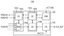
도 2를 참조하면, 본 발명의 일 실시예에 따른 클럭 신호 출력 회로(140)는 클럭 컴포넌트(141a, 141b), 유한 상태 기계(Finite State Machine, FSM)(143) 및 클럭 게이팅 회로(145)를 포함한다.Referring to FIG. 2 , a clock
클럭 컴포넌트(141a)는 클럭 제어 회로(Clock Control circuit, CC)(142a) 및 클럭 소오스(Clock Source, CS)(144a)를 포함한다. 여기서 클럭 소오스(144a)는 복수의 클럭 신호(CLK[n:0])를 입력받고 그 중 하나의 클럭 신호를 선택하는 다중화 회로(Multiplexer, MUX)를 포함한다. 클럭 제어 회로(142a)는 클럭 소오스(144a)를 하드웨어적으로 제어하고, 클럭 제어 회로(122a, 122b, 122c, 122d, 122e, 122f, 122g)에 하나 이상의 클럭 요청(REQ[n:0])을 전송하고, 이들로부터 하나 이상의 애크(ACK[n:0])를 수신한다.The
클럭 컴포넌트(141b)는 클럭 제어 회로(Clock Control circuit, CC)(142b) 및 클럭 소오스(Clock Source, CS)(144b)를 포함한다. 여기서 클럭 소오스(144b)는 클럭 소오스(144a)로부터 출력된 클럭 신호를 분주하는 분주 회로(Clock Dividing circuit, CD)를 포함한다. 클럭 소오스(144a)로부터 출력된 클럭 신호는 반도체 장치(1)의 출력 핀(150)이 동작하기 어려운 높은 주파수를 가질 수 있기 때문에, 클럭 소오스(144b)는 클럭 소오스(144a)로부터 출력된 클럭 신호의 주파수를 낮출 수 있다. 클럭 제어 회로(142b)는 클럭 소오스(144b)를 하드웨어적으로 제어하고, 클럭 제어 회로(142a)에 클럭 요청을 전송하고, 클럭 제어 회로(142a)로부터 애크를 수신한다.The
유한 상태 기계(143)는 동작 모드 제어 신호(Mode-control Signal, MS)에 따라 클럭 신호 출력 회로(140)의 동작 상태를 결정한다. 클럭 신호 출력 회로(140)는 클럭 소오스(124a, 124b, 124c, 124d, 124e, 124f, 124g)로부터 출력된 복수의 클럭 신호 중 어느 하나의 클럭 신호를 모니터링하는 "모니터링 모드"로 동작하거나, 상기 어느 하나의 클럭 신호를 반도체 장치(1) 외부에 구비된 임의의 장치에 전송하는 "기능 모드"로 동작할 수 있다.The
클럭 게이팅 회로(145)는 인에이블 신호(Enable signal, EN)에 따라 클럭 신호 출력 회로(140)에서 출력되는 클럭 신호(CLK_OUT)를 게이팅하여, 클럭 신호 출력 회로(140)를 사용하지 않는 경우 불필요한 클럭 신호의 출력을 방지한다.The
본 발명의 몇몇의 실시예에서, 동작 모드 제어 신호(MS) 및 인에이블 신호(EN)는 SFR(Special Fuction Register)을 이용하여 소프트웨어에 의해 제공될 수 있다. 그러나 본 발명의 범위는 이에 제한되는 것은 아니고, 동작 모드 제어 신호(MS) 및 인에이블 신호(EN)를 생성하는 제어 회로가 반도체 장치(1)에 구현될 수도 있다.In some embodiments of the present invention, the operation mode control signal MS and the enable signal EN may be provided by software using a special function register (SFR). However, the scope of the present invention is not limited thereto, and a control circuit generating an operation mode control signal MS and an enable signal EN may be implemented in the
도 3는 본 발명의 일 실시예에 따른 클럭 신호 출력 회로의 동작 방법을 설명하기 위한 개략도이다.3 is a schematic diagram illustrating an operating method of a clock signal output circuit according to an embodiment of the present invention.
도 3을 참조하면, 본 발명의 일 실시예에 따른 클럭 신호 출력 회로(140)는 기능 모드로 동작할 수 있다. 클럭 신호 출력 회로(140)가 반도체 장치(1) 외부에 구비된 임의의 장치를 구동하기 위한 클럭 신호를 제공하는 기능 모드로 동작하는 경우, 클럭 신호 출력 회로(140)는 도 1과 관련하여 설명한 클럭 컴포넌트로서 동작하게 된다.Referring to FIG. 3 , the clock
구체적으로, 기능 모드에서 클럭 신호 출력 회로(140)는 부모 클럭 컴포넌트(120b, 120c, 120d, 120e)에 클럭 요청(REQ[3:0])을 전송하고, 이에 대한 애크(ACK[3:0])를 수신할 수 있다. 즉, 반도체 장치(1) 외부에 구비된 임의의 장치를 구동하기 위해 클럭 신호 출력 회로(140)는 스스로 부모 클럭 컴포넌트(120b, 120c, 120d, 120e)에 클럭 요청(REQ[3:0])을 할 수 있다.Specifically, in the function mode, the clock
클럭 신호 출력 회로(140)로부터 전송된 클럭 요청(REQ[3:0])은 각각의 부모 클럭 컴포넌트(120b, 120c, 120d, 120e)에 전달된다. 예를 들어, 클럭 요청(REQ[3])은 부모 클럭 컴포넌트(120b)에 전달되고, 클럭 요청(REQ[2])은 부모 클럭 컴포넌트(120c)에 전달된다. 각각의 부모 클럭 컴포넌트(120b, 120c, 120d, 120e)로부터 전송된 각각의 애크(ACK[3:0])는 클럭 신호 출력 회로(140)에 전달된다. 예를 들어, 부모 클럭 컴포넌트(120b)로부터 출력된 애크(ACK[3])와 부모 클럭 컴포넌트(120c)로부터 출력된 애크(ACK[2])는 클럭 신호 출력 회로(140)에 전달된다.The clock request (REQ[3:0]) transmitted from the clock
한편, 클럭 신호 출력 회로(140)는 각각의 부모 클럭 컴포넌트(120b, 120c, 120d, 120e)로부터 수신한 클럭 신호(CLK[0], CLK[1], CLK[2], CLK[3]) 중 어느 하나를 선택하여 출력 핀(150)에 출력한다.Meanwhile, the clock
도 4는 본 발명의 다른 실시예에 따른 클럭 신호 출력 회로의 동작 방법을 설명하기 위한 개략도이다.4 is a schematic diagram illustrating an operating method of a clock signal output circuit according to another embodiment of the present invention.
도 4를 참조하면, 본 발명의 일 실시예에 따른 클럭 신호 출력 회로(140)는 모니터링 모드로 동작할 수 있다. 클럭 신호 출력 회로(140)가 단순히 반도체 장치(1) 내부의 클럭 신호들을 모니터링하기 위한 모니터링 모드로 동작하는 경우, 클럭 신호 출력 회로(140)는 부모 클럭 컴포넌트(120b, 120c, 120d, 120e)에 어떠한 클럭 요청도 전송하지 않는다. 클럭 신호 출력 회로(140)가 부모 클럭 컴포넌트(120b, 120c, 120d, 120e) 중 어느 하나에 클럭 요청을 하게 되면, 반도체 장치(1) 내부의 클럭 신호에 대한 환경(configuration)이 변경되어 모니터링을 정확하게 할 수 없기 때문이다.Referring to FIG. 4 , the clock
클럭 신호 출력 회로(140)는 각각의 부모 클럭 컴포넌트(120b, 120c, 120d, 120e)로부터 수신한 클럭 신호(CLK[0], CLK[1], CLK[2], CLK[3]) 중 어느 하나를 선택하여 출력 핀(150)에 출력한다.The clock
도 5는 본 발명의 또 다른 실시예에 따른 클럭 신호 출력 회로의 동작 방법을 설명하기 위한 개략도이다.5 is a schematic diagram illustrating an operating method of a clock signal output circuit according to another embodiment of the present invention.
도 5를 참조하면, 클럭 신호 출력 회로(140)의 클럭 소오스(144a)는 다중 회로를 포함하므로, 클럭 소오스(144a)는 클럭 제어 회로(142a)로부터 제공되는 선택 신호(SEL)에 의해 복수의 입력, 즉, 복수의 클럭 신호(CLK[n:0]) 중 어느 입력을 선택할 것인지를 결정한다.Referring to FIG. 5 , since the
반도체 장치(1)가 동작하는 중, 선택 신호(SEL)의 값을 변경해야 할 필요가 있는 경우, 클럭 신호 출력 회로(140)의 클럭 제어 회로(142a)는 부모 클럭 제어 회로에 클럭 요청(REQ)을 전송해야 한다. 이를 위해 클럭 신호 출력 회로(140)의 클럭 제어 회로(142a)는 부모 클럭 제어 회로에 전송할 클럭 요청(REQ)을 자체적으로 생성할 수 있다.While the
구체적으로, 클럭 신호 출력 회로(140)의 부모가 현재 클럭 소오스(144a)에 클럭 신호를 제공하고 있는 제1 부모(P1)(170)와 앞으로 클럭 소오스(144a)에 클럭 신호를 제공하기를 원하는 제2 부모(P2)(172)를 포함하는 경우, 선택 신호(SEL)의 값을 변경하여 제1 부모(170)로부터 제공받던 클럭 신호를 비선택하고 제2 부모(172)에 의해 제공받을 수 있는 클럭 신호를 선택하려면, 클럭 제어 회로(142a)는 부모(170, 172) 모두에게 클럭 요청(REQ)을 전송한다. 이에 따라 부모(170, 172) 모두로부터 클럭 소오스(144a)에 클럭이 제공되고 있음이 보장되면, 클럭 신호 출력 회로(140)의 클럭 제어 회로(142a)는 변경된 값을 갖는 선택 신호(SEL)를 클럭 소오스(144a)에 제공할 수 있다.Specifically, the parent of the clock
부모(170, 172) 모두로부터 클럭 소오스(144a)에 클럭이 제공되고 있음은 부모(170, 172)의 클럭 제어 회로로부터 수신되는 각각의 애크(ACK)를 통해 알 수 있다. 즉, 클럭 소오스(144a)는 클럭 제어 회로(142a)가 부모(170, 172)의 클럭 제어 회로로부터 클럭 요청(REQ)에 대한 각각의 애크(ACK)를 수신한 후, 변경된 선택 신호(SEL)에 따라 선택을 변경할 수 있다.It can be known that clocks are provided to the
도 6은 본 발명의 또 다른 실시예에 따른 클럭 신호 출력 회로의 동작 방법을 설명하기 위한 개략도이다.6 is a schematic diagram illustrating an operating method of a clock signal output circuit according to another embodiment of the present invention.
도 6을 참조하면, 클럭 신호 출력 회로(140)의 클럭 소오스(144b)는 클럭 분주 회로를 포함하므로, 클럭 소오스(144b)는 클럭 제어 회로(142b)로부터 제공되는 분주율(D_VAL)에 의해 클럭 소오스(144a)로부터 출력된 클럭 신호(CLK)를 분주하여 분주된 클럭 신호(D_CLK)를 생성할 수 있다.Referring to FIG. 6, since the
반도체 장치(1)가 동작하는 중, 분주율(D_VAL)의 값을 변경해야 할 필요가 있는 경우, 클럭 신호 출력 회로(140)의 클럭 제어 회로(142b)는 클럭 제어 회로(142a)에 클럭 요청(REQ)을 전송해야 한다. 이를 위해 클럭 신호 출력 회로(140)의 클럭 제어 회로(142b)는 클럭 제어 회로(142a)에 전송할 클럭 요청(REQ)을 자체적으로 생성할 수 있다.While the
이에 따라 클럭 소오스(144a)로부터 클럭 소오스(144b)에 클럭이 제공되고 있음이 보장되면, 클럭 신호 출력 회로(140)의 클럭 제어 회로(142b)는 변경된 값을 갖는 분주율(D_VAL)을 클럭 소오스(144b)에 제공할 수 있다.Accordingly, when it is ensured that the clock is supplied from the
클럭 소오스(144a)로부터 클럭 소오스(144b)에 클럭이 제공되고 있음은 클럭 제어 회로(142a)로부터 수신되는 애크(ACK)를 통해 알 수 있다. 즉, 클럭 소오스(144b)는 클럭 제어 회로(142b)가 클럭 제어 회로(142a)로부터 클럭 요청(REQ)에 대한 애크(ACK)를 수신한 후, 변경된 분주율(D_VAL)에 따라 클럭 신호(CLK)를 분주할 수 있다.The fact that the clock is supplied from the
도 7은 본 발명의 몇몇의 실시예에 따른 반도체 장치 및 반도체 장치의 동작 방법이 적용될 수 있는 반도체 시스템의 블록도이다.7 is a block diagram of a semiconductor system to which a semiconductor device and a method of operating the semiconductor device according to some embodiments of the present disclosure may be applied.
도 7을 참조하면, 본 발명의 몇몇의 실시예에 따른 반도체 장치 및 반도체 장치의 동작 방법이 적용될 수 있는 반도체 시스템은 앞서 설명한 바와 같은 특징들을 포함하는 반도체 장치(SoC)(1), 프로세서(10), 메모리 장치(20), 디스플레이 장치(30), 네트워크 장치(40), 스토리지 장치(50) 및 입출력 장치(60)를 포함할 수 있다. 반도체 장치(SoC)(1), 프로세서(10), 메모리 장치(20), 디스플레이 장치(30), 네트워크 장치(40), 스토리지 장치(50) 및 입출력 장치(60)는 버스(70)를 통해 서로 데이터를 주고 받을 수 있다.Referring to FIG. 7 , a semiconductor system to which a semiconductor device and a method of operating the semiconductor device according to some embodiments of the present invention may be applied include a semiconductor device (SoC) 1 including the features described above, and a processor 10 ), a
본 발명의 다양한 실시예에서 언급된 반도체 장치(SoC)(1) 내부의 IP 블록들은 메모리 장치(20)를 제어하는 메모리 컨트롤러, 디스플레이 장치(30)를 제어하는 디스플레이 컨트롤러, 네크워크 장치(40)를 제어하는 네트워크 컨트롤러, 스토리지 장치(50)를 제어하는 스토리지 컨트롤러 및 입출력 장치(60)를 제어하는 입출력 컨트롤러 중 적어도 하나를 포함할 수 있다. 또한 반도체 시스템은 이들 장치들을 제어하는 추가적인 프로세서(10)를 더 구비할 수도 있다.IP blocks inside the semiconductor device (SoC) 1 mentioned in various embodiments of the present invention include a memory controller for controlling the
이상 첨부된 도면을 참조하여 본 발명의 실시예들을 설명하였으나, 본 발명은 상기 실시예들에 한정되는 것이 아니라 서로 다른 다양한 형태로 제조될 수 있으며, 본 발명이 속하는 기술분야에서 통상의 지식을 가진 자는 본 발명의 기술적 사상이나 필수적인 특징을 변경하지 않고서 다른 구체적인 형태로 실시될 수 있다는 것을 이해할 수 있을 것이다. 그러므로 이상에서 기술한 실시예들은 모든 면에서 예시적인 것이며 한정적이 아닌 것으로 이해해야만 한다.Although the embodiments of the present invention have been described with reference to the accompanying drawings, the present invention is not limited to the above embodiments and can be manufactured in a variety of different forms, and those skilled in the art in the art to which the present invention belongs A person will understand that the present invention may be embodied in other specific forms without changing the technical spirit or essential features. Therefore, the embodiments described above should be understood as illustrative in all respects and not limiting.
1: 반도체 장치100: 클럭 관리 유닛(CMU)
110: 클럭 관리 유닛 컨트롤러(CMU controller)
120: 클럭 컴포넌트122: 클럭 제어 회로
124: 클럭 소오스130, 132: 채널 관리 회로
200, 210: IP 블록300: 전력 관리 유닛(PMU)1: semiconductor device 100: clock management unit (CMU)
110: clock management unit controller (CMU controller)
120: clock component 122: clock control circuit
124:
200, 210: IP Block 300: Power Management Unit (PMU)
Claims (20)
Translated fromKoreanIP 블록(Intellectual Property block)으로부터 수신된 IP 블록 클럭 요청에 대한 응답으로 상기 제1 클럭 제어 회로에 제1 클럭 요청을 전송하고, 상기 제1 클럭 소오스로부터 제1 클럭 신호를 제공받는 제2 클럭 소오스를 제어하는 제2 클럭 제어 회로; 및
상기 제1 클럭 소오스로부터 출력된 제1 클럭 신호 및 상기 제2 클럭 소오스로부터 출력된 제2 클럭 신호를 입력받고 상기 제1 클럭 신호 또는 상기 제2 클럭 신호를 출력 핀에 출력하는 클럭 신호 출력 회로를 포함하는 반도체 장치.a first clock control circuit for controlling a first clock source;
A second clock source that transmits a first clock request to the first clock control circuit in response to an IP block clock request received from an IP block (Intellectual Property block) and receives a first clock signal from the first clock source. a second clock control circuit for controlling; and
a clock signal output circuit receiving a first clock signal output from the first clock source and a second clock signal output from the second clock source and outputting the first clock signal or the second clock signal to an output pin; A semiconductor device comprising:
상기 클럭 신호 출력 회로는 동작 모드 제어 신호를 입력받아 모니터링 모드 또는 기능 모드로 동작하는 반도체 장치.According to claim 1,
The clock signal output circuit receives an operation mode control signal and operates in a monitoring mode or a function mode.
상기 클럭 신호 출력 회로가 상기 기능 모드로 동작하는 경우, 상기 클럭 신호 출력 회로는 상기 제1 클럭 제어 회로 또는 상기 제2 클럭 제어 회로에 제2 클럭 요청을 전송하는 반도체 장치.According to claim 2,
When the clock signal output circuit operates in the function mode, the clock signal output circuit transmits a second clock request to the first clock control circuit or the second clock control circuit.
상기 클럭 신호 출력 회로가 상기 모니터링 모드로 동작하는 경우, 상기 클럭 신호 출력 회로는 상기 제1 클럭 제어 회로 또는 상기 제2 클럭 제어 회로에 상기 제2 클럭 요청을 전송하지 않는 반도체 장치.According to claim 3,
When the clock signal output circuit operates in the monitoring mode, the clock signal output circuit does not transmit the second clock request to the first clock control circuit or the second clock control circuit.
상기 클럭 신호 출력 회로는 상기 제1 클럭 신호 및 상기 제2 클럭 신호 중 하나를 선택하여 출력하기 위한 다중화 회로(MUX circuit) 및 상기 다중화 회로를 제어하는 제3 클럭 제어 회로를 포함하는 반도체 장치.According to claim 2,
The semiconductor device of claim 1 , wherein the clock signal output circuit includes a multiplexing circuit (MUX circuit) for selecting and outputting one of the first clock signal and the second clock signal, and a third clock control circuit controlling the multiplexing circuit.
상기 다중화 회로가 상기 제1 클럭 신호 및 상기 제2 클럭 신호에 대한 선택을 변경하는 경우, 상기 제3 클럭 제어 회로는 상기 제1 클럭 제어 회로 및 상기 제2 클럭 제어 회로에 제3 클럭 요청 및 제4 클럭 요청을 각각 전송하는 반도체 장치.According to claim 5,
When the multiplexing circuit changes the selection of the first clock signal and the second clock signal, the third clock control circuit requests a third clock and a second clock control circuit to the first clock control circuit and the second clock control circuit. A semiconductor device that transmits each of the 4 clock requests.
상기 클럭 신호 출력 회로는 상기 다중화 회로로부터 출력된 클럭 신호를 분주하기 위한 클럭 분주 회로(clock dividing circuit) 및 상기 클럭 분주 회로를 제어하는 제4 클럭 제어 회로를 더 포함하는 반도체 장치.According to claim 5,
The semiconductor device of claim 1 , wherein the clock signal output circuit further includes a clock dividing circuit dividing the clock signal output from the multiplexing circuit and a fourth clock control circuit controlling the clock dividing circuit.
상기 분주 회로가 분주율(dividing ratio)을 변경하는 경우, 상기 제4 클럭 제어 회로는 상기 제3 클럭 제어 회로에 제5 클럭 요청을 전송하는 반도체 장치.According to claim 7,
When the dividing circuit changes a dividing ratio, the fourth clock control circuit transmits a fifth clock request to the third clock control circuit.
상기 클럭 신호 출력 회로는 상기 출력 핀에 출력되는 클럭 신호를 게이팅하기 위한 클럭 게이팅 회로를 포함하는 반도체 장치.According to claim 1,
The semiconductor device of claim 1 , wherein the clock signal output circuit includes a clock gating circuit for gating a clock signal output to the output pin.
상기 제1 클럭 소오스 또는 상기 제2 클럭 소오스는 다중화 회로(MUX circuit), 클럭 분주 회로(clock dividing circuit), 단기 정지 회로(short stop circuit) 및 클럭 게이팅 회로(clock gating circuit) 중 적어도 하나를 포함하는 반도체 장치.According to claim 1,
The first clock source or the second clock source includes at least one of a MUX circuit, a clock dividing circuit, a short stop circuit, and a clock gating circuit. semiconductor device.
IP 블록(Intellectual Property block)으로부터 수신된 IP 블록 클럭 요청에 대한 응답으로 상기 제1 클럭 제어 회로에 제1 클럭 요청을 전송하고, 상기 제1 클럭 소오스로부터 제1 클럭 신호를 제공받는 제2 클럭 소오스를 제어하는 제2 클럭 제어 회로; 및
상기 제1 클럭 소오스로부터 출력된 제1 클럭 신호 및 상기 제2 클럭 소오스로부터 출력된 제2 클럭 신호를 입력받는 다중화 회로(MUX circuit)를 제어하는 제3 클럭 제어 회로 및 상기 다중화 회로로부터 출력된 클럭 신호를 분주하는 클럭 분주 회로(clock dividing circuit)를 제어하는 제4 클럭 제어 회로를 포함하는 클럭 신호 출력 회로를 포함하는 반도체 장치.a first clock control circuit for controlling a first clock source;
A second clock source that transmits a first clock request to the first clock control circuit in response to an IP block clock request received from an IP block (Intellectual Property block) and receives a first clock signal from the first clock source. a second clock control circuit for controlling; and
A third clock control circuit for controlling a multiplexing circuit (MUX circuit) receiving the first clock signal output from the first clock source and the second clock signal output from the second clock source and a clock output from the multiplexing circuit A semiconductor device comprising a clock signal output circuit including a fourth clock control circuit for controlling a clock dividing circuit dividing a signal.
상기 클럭 신호 출력 회로는 동작 모드 제어 신호를 입력받아 모니터링 모드 또는 기능 모드로 동작하는 반도체 장치.According to claim 11,
The clock signal output circuit receives an operation mode control signal and operates in a monitoring mode or a function mode.
상기 SoC와 전기적으로 접속된 하나 이상의 외부 장치(external device)를 포함하고,
상기 클럭 관리 유닛은,
제1 클럭 소오스(clock source)를 제어하는 제1 클럭 제어 회로(clock control circuit);
IP 블록(Intellectual Property block)으로부터 수신된 IP 블록 클럭 요청에 대한 응답으로 상기 제1 클럭 제어 회로에 제1 클럭 요청을 전송하고, 상기 제1 클럭 소오스로부터 제1 클럭 신호를 제공받는 제2 클럭 소오스를 제어하는 제2 클럭 제어 회로; 및
상기 제1 클럭 소오스로부터 출력된 제1 클럭 신호 및 상기 제2 클럭 소오스로부터 출력된 제2 클럭 신호를 입력받고 상기 제1 클럭 신호 또는 상기 제2 클럭 신호를 상기 SoC의 출력 핀에 출력하는 클럭 신호 출력 회로를 포함하는 반도체 시스템.A System-on-Chip (SoC) including one or more Intellectual Property blocks (IP blocks) and a Clock Management Unit (CMU) providing clock signals to the IP blocks; and
Including one or more external devices electrically connected to the SoC,
The clock management unit,
a first clock control circuit that controls a first clock source;
A second clock source that transmits a first clock request to the first clock control circuit in response to an IP block clock request received from an IP block (Intellectual Property block) and receives a first clock signal from the first clock source. a second clock control circuit for controlling; and
A clock signal receiving the first clock signal output from the first clock source and the second clock signal output from the second clock source and outputting the first clock signal or the second clock signal to an output pin of the SoC A semiconductor system including an output circuit.
상기 클럭 신호 출력 회로는 동작 모드 제어 신호를 입력받아 모니터링 모드 또는 기능 모드로 동작하는 반도체 시스템.According to claim 13,
The semiconductor system according to claim 1 , wherein the clock signal output circuit receives an operation mode control signal and operates in a monitoring mode or a function mode.
제3 클럭 제어 회로에 의해 제어되는 다중화 회로(MUX circuit)를 이용하여 상기 제1 클럭 신호 및 상기 제2 클럭 신호 중 어느 하나를 선택하고,
제4 클럭 제어 회로에 의해 제어되는 클럭 분주 회로(clock dividing circuit)를 상기 선택된 클럭 신호를 분주하고,
상기 분주된 클럭 신호를 출력 핀에 출력하는 것을 포함하되,
상기 제2 클럭 제어 회로는 상기 제1 클럭 제어 회로에 제1 클럭 요청을 전송하고, 상기 제2 클럭 소오스는 상기 제1 클럭 소오스로부터 출력된 클럭 신호를 입력받는 반도체 장치의 동작 방법.receiving a first clock signal and a second clock signal respectively output from a first clock source controlled by the first clock control circuit and a second clock source controlled by the second clock control circuit;
Selecting one of the first clock signal and the second clock signal using a multiplexing circuit (MUX circuit) controlled by a third clock control circuit;
dividing the selected clock signal by a clock dividing circuit controlled by a fourth clock control circuit;
Outputting the divided clock signal to an output pin,
The second clock control circuit transmits a first clock request to the first clock control circuit, and the second clock source receives the clock signal output from the first clock source.
모니터링 모드 또는 기능 모드를 결정하는 동작 모드 제어 신호를 입력받는 것을 더 포함하는 반도체 장치의 동작 방법.According to claim 15,
A method of operating a semiconductor device, further comprising receiving an operation mode control signal for determining a monitoring mode or a function mode.
상기 기능 모드에서, 상기 제1 클럭 제어 회로 또는 상기 제2 클럭 제어 회로에 제2 클럭 요청을 전송하는 것을 더 포함하는 반도체 장치의 동작 방법.According to claim 16,
and transmitting a second clock request to the first clock control circuit or the second clock control circuit in the function mode.
상기 모니터링 모드에서, 클럭 게이팅 회로를 이용하여 상기 출력 핀에 출력되는 클럭 신호를 게이팅하는 것을 더 포함하는 반도체 장치의 동작 방법.According to claim 16,
and gating a clock signal output to the output pin using a clock gating circuit in the monitoring mode.
상기 제1 클럭 신호 및 상기 제2 클럭 신호 중 어느 하나를 선택하는 것은,
상기 제1 클럭 신호를 선택하고,
제3 클럭 요청 및 제4 클럭 요청을 상기 제3 클럭 제어 회로로부터 상기 제1 클럭 제어 회로 및 상기 제2 클럭 제어 회로에 전송하고,
상기 제2 클럭 신호를 선택하는 것을 더 포함하는 반도체 장치의 동작 방법.According to claim 15,
Selecting one of the first clock signal and the second clock signal,
select the first clock signal;
send a third clock request and a fourth clock request from the third clock control circuit to the first clock control circuit and the second clock control circuit;
The method of operating the semiconductor device further comprising selecting the second clock signal.
상기 선택된 클럭 신호를 분주하는 것은,
제5 클럭 요청을 상기 제4 클럭 제어 회로로부터 상기 제3 클럭 제어 회로에 전송하고,
상기 분주 회로의 분주율(dividing ratio)을 변경하는 것을 더 포함하는 반도체 장치의 동작 방법.According to claim 15,
Dividing the selected clock signal,
send a fifth clock request from the fourth clock control circuit to the third clock control circuit;
The method of operating the semiconductor device further comprising changing a dividing ratio of the dividing circuit.
Priority Applications (10)
| Application Number | Priority Date | Filing Date | Title |
|---|---|---|---|
| US15/415,106US10296066B2 (en) | 2016-01-25 | 2017-01-25 | Semiconductor device, semiconductor system, and method of operating the semiconductor device |
| US15/414,969US10296065B2 (en) | 2016-01-25 | 2017-01-25 | Clock management using full handshaking |
| DE102017110823.8ADE102017110823A1 (en) | 2016-01-25 | 2017-05-18 | Semiconductor device, semiconductor system and method of operating the semiconductor device |
| DE102017110821.1ADE102017110821A1 (en) | 2016-01-25 | 2017-05-18 | Semiconductor device |
| TW106116978ATWI747904B (en) | 2016-01-25 | 2017-05-23 | System on chip, clock gating component, multiplexer component and dividing component |
| TW106117999ATWI756225B (en) | 2016-01-25 | 2017-06-01 | System on chip, semiconductor system and clock signal output circuit |
| CN201710608439.6ACN108345350B (en) | 2016-01-25 | 2017-07-24 | System-on-chip, semiconductor system, and clock signal output circuit |
| US16/416,600US10969854B2 (en) | 2016-01-25 | 2019-05-20 | Semiconductor device including clock management unit for outputing clock and acknowledgement signals to an intellectual property block |
| US17/159,318US11340685B2 (en) | 2016-01-25 | 2021-01-27 | Semiconductor device including clock management unit for outputting clock and acknowledgment signals to an intelectual property block |
| US17/731,953US11789515B2 (en) | 2016-01-25 | 2022-04-28 | Semiconductor device |
Applications Claiming Priority (2)
| Application Number | Priority Date | Filing Date | Title |
|---|---|---|---|
| US201662286873P | 2016-01-25 | 2016-01-25 | |
| US62/286,873 | 2016-01-25 |
Publications (2)
| Publication Number | Publication Date |
|---|---|
| KR20170088767A KR20170088767A (en) | 2017-08-02 |
| KR102474620B1true KR102474620B1 (en) | 2022-12-05 |
Family
ID=59651738
Family Applications (1)
| Application Number | Title | Priority Date | Filing Date |
|---|---|---|---|
| KR1020170010943AActiveKR102474620B1 (en) | 2016-01-25 | 2017-01-24 | Semiconductor device, semiconductor system and method for operating semiconductor device |
Country Status (3)
| Country | Link |
|---|---|
| KR (1) | KR102474620B1 (en) |
| CN (1) | CN108345350B (en) |
| TW (1) | TWI756225B (en) |
Cited By (1)
| Publication number | Priority date | Publication date | Assignee | Title |
|---|---|---|---|---|
| KR102715967B1 (en) | 2023-10-13 | 2024-10-11 | 주식회사 잇다반도체 | Clock control circuit, and system-on chip device including the same |
Citations (2)
| Publication number | Priority date | Publication date | Assignee | Title |
|---|---|---|---|---|
| JP2002049437A (en) | 2000-08-01 | 2002-02-15 | Fujitsu Ltd | Electronic device and clock supply method |
| US20110202788A1 (en) | 2010-02-12 | 2011-08-18 | Blue Wonder Communications Gmbh | Method and device for clock gate controlling |
Family Cites Families (12)
| Publication number | Priority date | Publication date | Assignee | Title |
|---|---|---|---|---|
| WO2003021800A1 (en)* | 2001-08-29 | 2003-03-13 | Analog Devices, Inc. | Methods and apparatus for clock and power control in wireless systems |
| US7426670B2 (en)* | 2002-12-20 | 2008-09-16 | Nxp B.V. | Connecting multiple test access port controllers on a single test access port |
| US8448002B2 (en)* | 2008-04-10 | 2013-05-21 | Nvidia Corporation | Clock-gated series-coupled data processing modules |
| WO2010082609A1 (en)* | 2009-01-14 | 2010-07-22 | ミツミ電機株式会社 | Protection/monitor circuit and battery pack |
| US8190931B2 (en)* | 2009-04-30 | 2012-05-29 | Texas Instruments Incorporated | Power management events profiling |
| US8549339B2 (en)* | 2010-02-26 | 2013-10-01 | Empire Technology Development Llc | Processor core communication in multi-core processor |
| US9286257B2 (en)* | 2011-01-28 | 2016-03-15 | Qualcomm Incorporated | Bus clock frequency scaling for a bus interconnect and related devices, systems, and methods |
| JPWO2014006722A1 (en)* | 2012-07-05 | 2016-06-02 | 富士通株式会社 | Semiconductor integrated circuit and control method thereof |
| US9383805B2 (en)* | 2013-03-12 | 2016-07-05 | Atmel Corporation | Generating clock on demand |
| KR102148806B1 (en)* | 2013-10-07 | 2020-08-28 | 에스케이하이닉스 주식회사 | Semiconductor device and semiconductor system with the same |
| KR101406087B1 (en)* | 2014-02-10 | 2014-06-11 | 엠텍비젼 주식회사 | Frequency Divider And Method For Dividing Frequency Of Frequency Divider |
| KR102290984B1 (en)* | 2014-09-30 | 2021-08-18 | 삼성전자주식회사 | System-on-chip to support full handshake and mobile device having the same |
- 2017
- 2017-01-24KRKR1020170010943Apatent/KR102474620B1/enactiveActive
- 2017-06-01TWTW106117999Apatent/TWI756225B/enactive
- 2017-07-24CNCN201710608439.6Apatent/CN108345350B/enactiveActive
Patent Citations (2)
| Publication number | Priority date | Publication date | Assignee | Title |
|---|---|---|---|---|
| JP2002049437A (en) | 2000-08-01 | 2002-02-15 | Fujitsu Ltd | Electronic device and clock supply method |
| US20110202788A1 (en) | 2010-02-12 | 2011-08-18 | Blue Wonder Communications Gmbh | Method and device for clock gate controlling |
Cited By (1)
| Publication number | Priority date | Publication date | Assignee | Title |
|---|---|---|---|---|
| KR102715967B1 (en) | 2023-10-13 | 2024-10-11 | 주식회사 잇다반도체 | Clock control circuit, and system-on chip device including the same |
Also Published As
| Publication number | Publication date |
|---|---|
| CN108345350B (en) | 2021-12-10 |
| KR20170088767A (en) | 2017-08-02 |
| TWI756225B (en) | 2022-03-01 |
| CN108345350A (en) | 2018-07-31 |
| TW201827978A (en) | 2018-08-01 |
Similar Documents
| Publication | Publication Date | Title |
|---|---|---|
| US10296066B2 (en) | Semiconductor device, semiconductor system, and method of operating the semiconductor device | |
| US9825755B2 (en) | Configurable clock tree | |
| TWI727075B (en) | Semiconductor device | |
| US10587265B2 (en) | Semiconductor device and semiconductor system | |
| US20170220495A1 (en) | Semiconductor device, a semiconductor system and a method for operating the semiconductor device | |
| KR102474620B1 (en) | Semiconductor device, semiconductor system and method for operating semiconductor device | |
| US10209734B2 (en) | Semiconductor device, semiconductor system, and method of operating the semiconductor device | |
| TWI752067B (en) | Semiconductor device and a semiconductor system | |
| US10248155B2 (en) | Semiconductor device including clock generating circuit and channel management circuit | |
| KR102740417B1 (en) | Semiconductor device, semiconductor system and method for operating semiconductor device | |
| KR102712345B1 (en) | Semiconductor device, semiconductor system and method for operating semiconductor device | |
| KR102550422B1 (en) | Semiconductor device | |
| US10429881B2 (en) | Semiconductor device for stopping an oscillating clock signal from being provided to an IP block, a semiconductor system having the semiconductor device, and a method of operating the semiconductor device | |
| KR102568225B1 (en) | Semiconductor device, semiconductor system and method for operating semiconductor device | |
| TWI771301B (en) | Semiconductor device and semiconductor system | |
| CN108268086B (en) | Semiconductor device, semiconductor system, and method of operating semiconductor device | |
| CN108268085B (en) | Semiconductor device | |
| CN108268117B (en) | Semiconductor device and semiconductor system | |
| CN108268087A (en) | Semiconductor device, semiconductor system and the method for operating semiconductor device | |
| JP2015158826A (en) | Transmission device |
Legal Events
| Date | Code | Title | Description |
|---|---|---|---|
| PA0109 | Patent application | Patent event code:PA01091R01D Comment text:Patent Application Patent event date:20170124 | |
| PG1501 | Laying open of application | ||
| A201 | Request for examination | ||
| PA0201 | Request for examination | Patent event code:PA02012R01D Patent event date:20210708 Comment text:Request for Examination of Application Patent event code:PA02011R01I Patent event date:20170124 Comment text:Patent Application | |
| E902 | Notification of reason for refusal | ||
| PE0902 | Notice of grounds for rejection | Comment text:Notification of reason for refusal Patent event date:20220817 Patent event code:PE09021S01D | |
| E701 | Decision to grant or registration of patent right | ||
| PE0701 | Decision of registration | Patent event code:PE07011S01D Comment text:Decision to Grant Registration Patent event date:20221025 | |
| GRNT | Written decision to grant | ||
| PR0701 | Registration of establishment | Comment text:Registration of Establishment Patent event date:20221201 Patent event code:PR07011E01D | |
| PR1002 | Payment of registration fee | Payment date:20221201 End annual number:3 Start annual number:1 | |
| PG1601 | Publication of registration |