KR102473167B1 - Nonvolatile memory device and erasing method thereof - Google Patents
Nonvolatile memory device and erasing method thereofDownload PDFInfo
- Publication number
- KR102473167B1 KR102473167B1KR1020150181882AKR20150181882AKR102473167B1KR 102473167 B1KR102473167 B1KR 102473167B1KR 1020150181882 AKR1020150181882 AKR 1020150181882AKR 20150181882 AKR20150181882 AKR 20150181882AKR 102473167 B1KR102473167 B1KR 102473167B1
- Authority
- KR
- South Korea
- Prior art keywords
- program
- voltage
- verification
- program loop
- cells
- Prior art date
- Legal status (The legal status is an assumption and is not a legal conclusion. Google has not performed a legal analysis and makes no representation as to the accuracy of the status listed.)
- Active
Links
- 238000000034methodMethods0.000titledescription19
- 238000012795verificationMethods0.000claimsabstractdescription113
- 230000008859changeEffects0.000abstractdescription5
- 238000009826distributionMethods0.000description21
- 238000010586diagramMethods0.000description18
- 239000004065semiconductorSubstances0.000description9
- 230000007423decreaseEffects0.000description7
- 239000000758substrateSubstances0.000description7
- 230000004044responseEffects0.000description6
- 101000641216Aquareovirus G (isolate American grass carp/USA/PB01-155/-) Non-structural protein 4Proteins0.000description4
- 238000012937correctionMethods0.000description4
- 101100049574Human herpesvirus 6A (strain Uganda-1102) U5 geneProteins0.000description3
- 238000004891communicationMethods0.000description3
- 230000006870functionEffects0.000description3
- 101150064834ssl1 geneProteins0.000description3
- 101150062870ssl3 geneProteins0.000description3
- 238000013519translationMethods0.000description3
- 101100152598Arabidopsis thaliana CYP73A5 geneProteins0.000description2
- 101100219315Arabidopsis thaliana CYP83A1 geneProteins0.000description2
- 101100512568Arabidopsis thaliana MED33B geneProteins0.000description2
- 101000927946Homo sapiens LisH domain-containing protein ARMC9Proteins0.000description2
- 102100036882LisH domain-containing protein ARMC9Human genes0.000description2
- 101100269674Mus musculus Alyref2 geneProteins0.000description2
- 101100140580Saccharomyces cerevisiae (strain ATCC 204508 / S288c) REF2 geneProteins0.000description2
- 230000005540biological transmissionEffects0.000description2
- 238000009413insulationMethods0.000description2
- 238000012545processingMethods0.000description2
- 239000007787solidSubstances0.000description2
- 238000012546transferMethods0.000description2
- 102100031885General transcription and DNA repair factor IIH helicase subunit XPBHuman genes0.000description1
- 101000806846Homo sapiens DNA-(apurinic or apyrimidinic site) endonucleaseProteins0.000description1
- 101000920748Homo sapiens General transcription and DNA repair factor IIH helicase subunit XPBProteins0.000description1
- 101000835083Homo sapiens Tissue factor pathway inhibitor 2Proteins0.000description1
- VYPSYNLAJGMNEJ-UHFFFAOYSA-NSilicium dioxideChemical compoundO=[Si]=OVYPSYNLAJGMNEJ-UHFFFAOYSA-N0.000description1
- XUIMIQQOPSSXEZ-UHFFFAOYSA-NSiliconChemical compound[Si]XUIMIQQOPSSXEZ-UHFFFAOYSA-N0.000description1
- 102100026134Tissue factor pathway inhibitor 2Human genes0.000description1
- 238000003491arrayMethods0.000description1
- 238000006243chemical reactionMethods0.000description1
- 230000000694effectsEffects0.000description1
- 230000006872improvementEffects0.000description1
- 239000011810insulating materialSubstances0.000description1
- 230000010354integrationEffects0.000description1
- 238000013507mappingMethods0.000description1
- 238000012986modificationMethods0.000description1
- 230000004048modificationEffects0.000description1
- 230000000149penetrating effectEffects0.000description1
- 238000002360preparation methodMethods0.000description1
- 238000011084recoveryMethods0.000description1
- 238000011160researchMethods0.000description1
- 229910052710siliconInorganic materials0.000description1
- 239000010703siliconSubstances0.000description1
- 229910052814silicon oxideInorganic materials0.000description1
Images


Classifications
- G—PHYSICS
- G11—INFORMATION STORAGE
- G11C—STATIC STORES
- G11C16/00—Erasable programmable read-only memories
- G11C16/02—Erasable programmable read-only memories electrically programmable
- G11C16/06—Auxiliary circuits, e.g. for writing into memory
- G11C16/34—Determination of programming status, e.g. threshold voltage, overprogramming or underprogramming, retention
- G11C16/3404—Convergence or correction of memory cell threshold voltages; Repair or recovery of overerased or overprogrammed cells
- G—PHYSICS
- G11—INFORMATION STORAGE
- G11C—STATIC STORES
- G11C16/00—Erasable programmable read-only memories
- G11C16/02—Erasable programmable read-only memories electrically programmable
- G11C16/06—Auxiliary circuits, e.g. for writing into memory
- G11C16/34—Determination of programming status, e.g. threshold voltage, overprogramming or underprogramming, retention
- G11C16/3436—Arrangements for verifying correct programming or erasure
- G11C16/3454—Arrangements for verifying correct programming or for detecting overprogrammed cells
- G11C16/3459—Circuits or methods to verify correct programming of nonvolatile memory cells
- G—PHYSICS
- G11—INFORMATION STORAGE
- G11C—STATIC STORES
- G11C16/00—Erasable programmable read-only memories
- G11C16/02—Erasable programmable read-only memories electrically programmable
- G11C16/06—Auxiliary circuits, e.g. for writing into memory
- G11C16/34—Determination of programming status, e.g. threshold voltage, overprogramming or underprogramming, retention
- G11C16/3436—Arrangements for verifying correct programming or erasure
- G11C16/3454—Arrangements for verifying correct programming or for detecting overprogrammed cells
- G—PHYSICS
- G11—INFORMATION STORAGE
- G11C—STATIC STORES
- G11C11/00—Digital stores characterised by the use of particular electric or magnetic storage elements; Storage elements therefor
- G11C11/56—Digital stores characterised by the use of particular electric or magnetic storage elements; Storage elements therefor using storage elements with more than two stable states represented by steps, e.g. of voltage, current, phase, frequency
- G11C11/5671—Digital stores characterised by the use of particular electric or magnetic storage elements; Storage elements therefor using storage elements with more than two stable states represented by steps, e.g. of voltage, current, phase, frequency using charge trapping in an insulator
- G—PHYSICS
- G11—INFORMATION STORAGE
- G11C—STATIC STORES
- G11C16/00—Erasable programmable read-only memories
- G11C16/02—Erasable programmable read-only memories electrically programmable
- G11C16/04—Erasable programmable read-only memories electrically programmable using variable threshold transistors, e.g. FAMOS
- G11C16/0408—Erasable programmable read-only memories electrically programmable using variable threshold transistors, e.g. FAMOS comprising cells containing floating gate transistors
- G11C16/0441—Erasable programmable read-only memories electrically programmable using variable threshold transistors, e.g. FAMOS comprising cells containing floating gate transistors comprising cells containing multiple floating gate devices, e.g. separate read-and-write FAMOS transistors with connected floating gates
- G—PHYSICS
- G11—INFORMATION STORAGE
- G11C—STATIC STORES
- G11C16/00—Erasable programmable read-only memories
- G11C16/02—Erasable programmable read-only memories electrically programmable
- G11C16/06—Auxiliary circuits, e.g. for writing into memory
- G11C16/08—Address circuits; Decoders; Word-line control circuits
- G—PHYSICS
- G11—INFORMATION STORAGE
- G11C—STATIC STORES
- G11C16/00—Erasable programmable read-only memories
- G11C16/02—Erasable programmable read-only memories electrically programmable
- G11C16/06—Auxiliary circuits, e.g. for writing into memory
- G11C16/10—Programming or data input circuits
- G—PHYSICS
- G11—INFORMATION STORAGE
- G11C—STATIC STORES
- G11C16/00—Erasable programmable read-only memories
- G11C16/02—Erasable programmable read-only memories electrically programmable
- G11C16/06—Auxiliary circuits, e.g. for writing into memory
- G11C16/34—Determination of programming status, e.g. threshold voltage, overprogramming or underprogramming, retention
- G11C16/3436—Arrangements for verifying correct programming or erasure
- G11C16/3468—Prevention of overerasure or overprogramming, e.g. by verifying whilst erasing or writing
- G11C16/3481—Circuits or methods to verify correct programming of nonvolatile memory cells whilst programming is in progress, e.g. by detecting onset or cessation of current flow in cells and using the detector output to terminate programming
- G—PHYSICS
- G11—INFORMATION STORAGE
- G11C—STATIC STORES
- G11C2211/00—Indexing scheme relating to digital stores characterized by the use of particular electric or magnetic storage elements; Storage elements therefor
- G11C2211/56—Indexing scheme relating to G11C11/56 and sub-groups for features not covered by these groups
- G11C2211/562—Multilevel memory programming aspects
- G11C2211/5621—Multilevel programming verification
- G—PHYSICS
- G11—INFORMATION STORAGE
- G11C—STATIC STORES
- G11C2211/00—Indexing scheme relating to digital stores characterized by the use of particular electric or magnetic storage elements; Storage elements therefor
- G11C2211/56—Indexing scheme relating to G11C11/56 and sub-groups for features not covered by these groups
- G11C2211/564—Miscellaneous aspects
- G11C2211/5644—Multilevel memory comprising counting devices
- G—PHYSICS
- G11—INFORMATION STORAGE
- G11C—STATIC STORES
- G11C2213/00—Indexing scheme relating to G11C13/00 for features not covered by this group
- G11C2213/70—Resistive array aspects
- G11C2213/75—Array having a NAND structure comprising, for example, memory cells in series or memory elements in series, a memory element being a memory cell in parallel with an access transistor
Landscapes
- Engineering & Computer Science (AREA)
- Computer Hardware Design (AREA)
- Read Only Memory (AREA)
- Microelectronics & Electronic Packaging (AREA)
Abstract
Translated fromKoreanDescription
Translated fromKorean본 발명은 반도체 메모리에 관한 것으로, 좀 더 구체적으로는 불휘발성 메모리 장치 및 그것의 프로그램 방법에 관한 것이다.The present invention relates to a semiconductor memory, and more particularly, to a nonvolatile memory device and a programming method thereof.
반도체 메모리 장치는 크게 휘발성 반도체 메모리 장치(volatile semiconductor memory device)와 불휘발성 반도체 메모리 장치(non-volatile semiconductor memory device)로 구분된다.Semiconductor memory devices are largely classified into volatile semiconductor memory devices and non-volatile semiconductor memory devices.
휘발성 반도체 메모리 장치는 읽고 쓰는 속도가 빠르지만 외부 전원 공급이 끊기면 저장된 내용이 사라져 버리는 단점이 있다. 반면에 불휘발성 반도체 메모리 장치는 외부 전원 공급이 중단되더라도 그 내용을 보존한다. 그러므로, 불휘발성 반도체 메모리 장치는 전원이 공급되었는지의 여부에 관계없이 보존되어야 할 내용을 기억시키는 데 쓰인다. 불휘발성 반도체 메모리 장치로는 마스크 롬(mask read-only memory, MROM), 프로그램 가능한 롬(programmable read-only memory, PROM), 소거 및 프로그램 가능한 롬(erasable programmable read-only memory, EPROM), 전기적으로 소거 및 프로그램 가능한 롬(electrically erasable programmable read-only memory, EEPROM) 등이 있다.A volatile semiconductor memory device has a high read/write speed, but has a disadvantage in that stored contents disappear when an external power supply is cut off. On the other hand, the nonvolatile semiconductor memory device retains its contents even if external power supply is interrupted. Therefore, nonvolatile semiconductor memory devices are used to store contents to be preserved regardless of whether power is supplied or not. Nonvolatile semiconductor memory devices include mask read-only memory (MROM), programmable read-only memory (PROM), erasable programmable read-only memory (EPROM), electrically and electrically erasable programmable read-only memory (EEPROM).
플래시 메모리 장치는, 각각의 메모리 셀에 저장되는 비트 수에 따라서 각각의 메모리 셀에 저장 가능한 데이터 상태가 결정된다. 하나의 메모리 셀에 1-비트 데이터를 저장하는 메모리 셀을 단일 비트 셀(single-bit cell) 또는 단일 레벨 셀(single-level cell ; SLC)이라 한다. 그리고, 하나의 메모리 셀에 멀티-비트 데이터(예를 들면, 2 비트 이상)를 저장하는 멀티 비트 셀(multi-bit cell), 멀티 레벨 셀(multi-level cell ; MLC), 또는 멀티 스테이트 셀(multi-state cell)이라 한다. 최근 들어, 메모리 장치에 대한 고집적 요구가 높아짐에 따라, 하나의 메모리 셀에 멀티-비트 데이터를 저장하는 멀티 레벨 플래시 메모리에 대한 연구가 활발히 진행되고 있다.In a flash memory device, the state of data that can be stored in each memory cell is determined according to the number of bits stored in each memory cell. A memory cell storing 1-bit data in one memory cell is referred to as a single-bit cell or a single-level cell (SLC). And, a multi-bit cell, a multi-level cell (MLC), or a multi-state cell (eg, 2 or more bits) storing multi-bit data (eg, 2 bits or more) in one memory cell. multi-state cell). Recently, as the demand for high integration of a memory device increases, research on a multi-level flash memory storing multi-bit data in one memory cell has been actively conducted.
본 발명의 목적은 메모리 셀들의 산포를 개선하는 불휘발성 메모리 장치 및 그것의 프로그램 방법을 제공하는 데 있다.SUMMARY OF THE INVENTION An object of the present invention is to provide a nonvolatile memory device and a method for programming the same, which improve the distribution of memory cells.
상기 목적을 해결하기 위한 본 발명에 따른 불휘발성 메모리 장치는 복수의 메모리 셀들을 포함하는 메모리 셀 어레이, 검증 동작 시 상기 메모리 셀들 중 선택된 메모리 셀들에 검증 전압을 제공하는 어드레스 디코더, 그리고 특정 시점 이후의 검증 동작에서 상기 검증 전압를 변경하도록 제어하는 제어 로직을 포함하되, 상기 제어 로직은 제 1 프로그램 루프의 검증 동작의 결과에 기초하여 상기 검증 전압이 변경되는 제 2 프로그램 루프를 검증 전압 오프셋 시점으로 결정한다.A nonvolatile memory device according to the present invention to solve the above object is a memory cell array including a plurality of memory cells, an address decoder providing a verify voltage to selected memory cells during a verify operation, and a and a control logic for controlling the verification voltage to be changed in a verification operation, wherein the control logic determines a second program loop in which the verification voltage is changed as a verification voltage offset time point based on a result of the verification operation of the first program loop. .
상기 목적을 해결하기 위한 본 발명에 따른 불휘발성 메모리 장치는 복수의 메모리 셀들을 포함하는 메모리 셀 어레이, 검증 동작 시 상기 메모리 셀들 중 선택된 메모리 셀들에 검증 전압을 제공하는 어드레스 디코더, 그리고 특정 시점 이후의 검증 동작에서 상기 검증 전압를 변경하도록 제어하는 제어 로직을 포함하되, 상기 제어 로직은 제 1 프로그램 루프의 검증 동작 시 특정 프로그램 상태의 프로그램 완료 여부에 기초하여 상기 검증 전압이 변경되는 제 2 프로그램 루프를 검증 전압 오프셋 시점으로 결정한다.A nonvolatile memory device according to the present invention to solve the above object is a memory cell array including a plurality of memory cells, an address decoder providing a verify voltage to selected memory cells during a verify operation, and a and a control logic for controlling the verification voltage to be changed in a verification operation, wherein the control logic verifies a second program loop in which the verification voltage is changed based on whether a program of a specific program state is completed during a verification operation of a first program loop. It is determined at the time of the voltage offset.
본 발명의 실시 예에 따르면, 복수의 프로그램 루프들 중에서 검증 전압에 오프셋을 적용하는 시점을 적응적으로 제어하여 메모리 셀들의 산포를 개선하는 불휘발성 메모리 장치 및 그것의 프로그램 방법을 제공하는 데 있다.According to an embodiment of the present invention, an object of the present invention is to provide a nonvolatile memory device and a program method thereof that improve distribution of memory cells by adaptively controlling timing at which offsets are applied to verification voltages among a plurality of program loops.
도 1은 본 발명에 따른 불휘발성 메모리 장치를 보여주는 블록도이다.
도 2는 프로그램 동작에 따라 메모리 셀들의 문턱 전압들이 형성되는 예를 보여준다.
도 3은 본 발명의 실시 예에 따른 불휘발성 메모리 장치의 프로그램 방법을 보여주는 도면이다.
도 4는 도 3의 검증 전압의 오프셋 시점을 적응적으로 결정하는 방법을 보여주는 도면이다.
도 5는 도 3의 검증 전압의 오프셋 시점을 적응적으로 결정하는 방법을 예시적으로 보여주는 표이다.
도 6은 본 발명의 다른 실시 예에 따른 불휘발성 메모리 장치의 프로그램 방법을 보여주는 도면이다.
도 7은 본 발명의 실시 예에 따른 검증 전압의 오프셋 시점을 적응적으로 결정하는 방법을 보여주는 순서도이다.
도 8은 도 1의 메모리 셀 어레이의 메모리 블록들 중 하나(BLKi)를 보여주는 회로도이다.
도 9는 도 8의 메모리 블록(BLKi)에 대응하는 구조의 실시 예를 보여주는 사시도이다.
도 10은 본 발명의 실시 예에 따른 솔리드 스테이트 드라이브를 예시적으로 보여주는 블록도이다.
도 11은 본 발명의 실시 예에 따른 eMMC를 예시적으로 보여주는 블록도이다.
도 12는 본 발명의 실시 예에 따른 UFS 시스템을 예시적으로 보여주는 블록도이다.
도 13은 본 발명의 실시 예에 따른 모바일 장치를 예시적으로 보여주는 블록도이다.1 is a block diagram showing a nonvolatile memory device according to the present invention.
2 shows an example in which threshold voltages of memory cells are formed according to a program operation.
3 is a diagram illustrating a programming method of a nonvolatile memory device according to an embodiment of the present invention.
FIG. 4 is a diagram illustrating a method of adaptively determining an offset timing of the verification voltage of FIG. 3 .
FIG. 5 is a table exemplarily illustrating a method of adaptively determining an offset timing of the verification voltage of FIG. 3 .
6 is a diagram illustrating a programming method of a nonvolatile memory device according to another embodiment of the present invention.
7 is a flowchart illustrating a method of adaptively determining an offset timing of a verification voltage according to an embodiment of the present invention.
FIG. 8 is a circuit diagram showing one of the memory blocks BLKi of the memory cell array of FIG. 1 .
FIG. 9 is a perspective view illustrating an embodiment of a structure corresponding to the memory block BLKi of FIG. 8 .
10 is a block diagram exemplarily showing a solid state drive according to an embodiment of the present invention.
11 is a block diagram exemplarily showing an eMMC according to an embodiment of the present invention.
12 is a block diagram exemplarily showing a UFS system according to an embodiment of the present invention.
13 is a block diagram showing a mobile device according to an embodiment of the present invention by way of example.
앞의 일반적인 설명 및 다음의 상세한 설명 모두 예시적이라는 것이 이해되어야 하며, 청구된 발명의 부가적인 설명이 제공되는 것으로 여겨져야 한다. 참조부호들이 본 발명의 바람직한 실시 예들에 상세히 표시되어 있으며, 그것의 예들이 참조 도면들에 표시되어 있다. 가능한 어떤 경우에도, 동일한 참조 번호들이 동일한 또는 유사한 부분을 참조하기 위해서 설명 및 도면들에 사용된다.It is to be understood that both the foregoing general description and the following detailed description are illustrative, and are to be considered as providing additional explanation of the claimed invention. Reference numerals are indicated in detail in the preferred embodiments of the present invention, examples thereof are indicated in the reference drawings. Wherever possible, the same reference numbers are used in the description and drawings to refer to the same or like parts.
이하에서는, 불휘발성 메모리 장치가 본 발명의 특징 및 기능을 설명하기 위한 저장 장치 또는 전자 장치의 한 예로서 사용될 것이다. 하지만, 이 기술 분야에 정통한 사람은 여기에 기재된 내용에 따라 본 발명의 다른 이점들 및 성능을 쉽게 이해할 수 있을 것이다. 또한, 본 발명은 다른 실시 예들을 통해 구현되거나 적용될 수 있을 것이다. 게다가, 상세한 설명은 본 발명의 범위, 기술적 사상 그리고 다른 목적으로부터 상당히 벗어나지 않고, 관점 및 응용에 따라 수정되거나 변경될 수 있다.Hereinafter, a nonvolatile memory device will be used as an example of a storage device or electronic device for describing features and functions of the present invention. However, those skilled in the art will readily appreciate other advantages and capabilities of the present invention in light of the disclosure herein. In addition, the present invention may be implemented or applied through other embodiments. In addition, the detailed description can be modified or changed according to viewpoints and applications without significantly departing from the scope, spirit, and other purposes of the present invention.
본 발명의 개념에 따른 실시 예로서, 3차원 메모리 어레이가 제공된다. 3차원 메모리 어레이는, 실리콘 기판 및 메모리 셀들의 동작에 연관된 회로의 위에 배치되는 활성 영역을 갖는 메모리 셀들의 어레이들의 하나 또는 그 이상의 물리 레벨들에 모놀리식으로(monolithically) 형성될 수 있다. 메모리 셀들의 동작에 연관된 회로는 기판 내에 또는 기판 위에 위치할 수 있다. 모놀리식(monolithical)이란 용어는, 3차원 어레이의 각 레벨의 층들이 3차원 어레이의 하위 레벨의 층들 위에 직접 증착됨을 의미한다.As an embodiment according to the concept of the present invention, a three-dimensional memory array is provided. A three-dimensional memory array may be monolithically formed on one or more physical levels of arrays of memory cells having an active region disposed over a silicon substrate and circuitry associated with operation of the memory cells. Circuitry involved in the operation of the memory cells may be located in or on the substrate. The term monolithical means that the layers of each level of the three-dimensional array are deposited directly over the layers of lower levels of the three-dimensional array.
본 발명의 개념에 따른 실시 예로서, 3차원 메모리 어레이는 수직의 방향성을 가져, 적어도 하나의 메모리 셀이 다른 하나의 메모리 셀 위에 위치하는 수직 NAND 스트링들을 포함한다. 적어도 하나의 메모리 셀은 전하 트랩 층을 포함한다. 각각의 수직 NAND 스트링은 메모리 셀들 위에 위치하는 적어도 하나의 선택 트랜지스터를 포함할 수 있다. 적어도 하나의 선택 트랜지스터는 메모리 셀들과 동일한 구조를 갖고, 메모리 셀들과 함께 모놀리식으로 형성될 수 있다.As an embodiment according to the concept of the present invention, a 3D memory array includes vertical NAND strings having a vertical direction, such that at least one memory cell is located above another memory cell. At least one memory cell includes a charge trap layer. Each vertical NAND string may include at least one select transistor located over the memory cells. At least one select transistor has the same structure as the memory cells and may be monolithically formed with the memory cells.
3차원 메모리 어레이가 복수의 레벨들로 구성되고, 레벨들 사이에 공유된 워드 라인들 또는 비트 라인들을 갖고, 3차원 메모리 어레이에 적합한 구성은 미국등록특허공보 제7,679,133호, 미국등록특허공보 제8,553,466호, 미국등록특허공보 제8,654,587호, 미국등록특허공보 제8,559,235호, 그리고 미국공개특허공보 제2011/0233648호에 개시되어 있으며, 본 발명의 레퍼런스로 포함된다.Configurations in which the three-dimensional memory array is composed of a plurality of levels, with word lines or bit lines shared between the levels, suitable for the three-dimensional memory array are disclosed in U.S. Patent No. 7,679,133 and U.S. Patent No. 8,553,466. , US Patent Publication No. 8,654,587, US Patent Publication No. 8,559,235, and US Patent Publication No. 2011/0233648, which are incorporated herein by reference.
도 1은 본 발명에 따른 불휘발성 메모리 장치를 보여주는 블록도이다. 도 1를 참조하면, 불휘발성 메모리 장치(100)는 메모리 셀 어레이(110), 어드레스 디코더(120), 전압 발생기(130), 입출력 회로(140), 및 제어 로직(150)을 포함할 수 있다.1 is a block diagram showing a nonvolatile memory device according to the present invention. Referring to FIG. 1 , a
메모리 셀 어레이(110)는 스트링 선택 라인들(String Select Line, SSL), 워드 라인들(Word Line, WL) 및 접지 선택 라인들(Ground Select Line, GSL)을 통해 어드레스 디코더(120)에 연결되고, 비트 라인들(Bit Line, BL)을 통해 입출력 회로(140)에 연결된다. 메모리 셀 어레이(110)는 복수의 메모리 블록들을 포함할 수 있다. 각 메모리 블록의 메모리 셀들은 2차원 구조를 형성할 수 있다. 또한, 각 메모리 블록의 메모리 셀들은 기판과 수직한 방향으로 적층되어 3차원 구조를 형성할 수 있다. 각 메모리 블록은 복수의 메모리 셀들 및 복수의 선택 트랜지스터들을 포함할 수 있다. 메모리 셀들은 워드 라인들(WL)에 연결되고, 선택 트랜지스터들은 스트링 선택 라인들(SSL) 또는 접지 선택 라인들(GSL)에 연결될 수 있다. 각 메모리 블록의 메모리 셀들은 하나 또는 그 이상의 비트를 저장할 수 있다.The
어드레스 디코더(120)는 스트링 선택 라인들(SSL), 워드 라인들(WL) 및 접지 선택 라인들(GSL)을 통해 메모리 셀 어레이(110)에 연결된다. 어드레스 디코더(120)는 제어 로직(150)의 제어에 응답하여 동작하도록 구성된다. 어드레스 디코더(120)는 외부로부터 어드레스(ADDR)를 수신한다.The
어드레스 디코더(120)는 수신된 어드레스(ADDR) 중 행 어드레스를 디코딩하도록 구성된다. 디코딩된 행 어드레스를 이용하여, 어드레스 디코더(120)는 스트링 선택 라인들(SSL), 워드 라인들(WL) 및 접지 선택 라인들(GSL)을 선택한다. 어드레스 디코더(120)는 전압 발생기(130)로부터 다양한 전압들을 수신하고, 수신된 전압들을 선택 및 비선택된 스트링 선택 라인들(SSL), 워드 라인들(WL) 및 접지 선택 라인들(GSL)에 각각 전달할 수 있다.The
어드레스 디코더(120)는 전달된 어드레스(ADDR) 중 열 어드레스를 디코딩하도록 구성될 수 있다. 디코딩된 열 어드레스는 입출력 회로(140)에 전달될 수 있다. 예시적으로, 어드레스 디코더(120)는 행 디코더, 열 디코더, 어드레스 버퍼 등과 같은 구성 요소들을 포함할 수 있다.The
전압 발생기(130)는 불휘발성 메모리 장치(100)에서 요구되는 다양한 전압들을 생성하도록 구성된다. 예를 들어, 전압 발생기(130)는 복수의 프로그램 전압들, 복수의 패스 전압들, 복수의 검증 전압들, 복수의 선택 읽기 전압들, 및 복수의 비선택 읽기 전압들을 생성할 수 있다.The
입출력 회로(140)는 비트 라인들(BL)을 통해 메모리 셀 어레이(110)에 연결되고, 외부와 데이터(DATA)를 교환할 수 있다. 입출력 회로(140)는 제어 로직(150)의 제어에 응답하여 동작한다.The input/
예시적으로, 입출력 회로(140)는 외부로부터 데이터(DATA)를 수신하고, 수신된 데이터(DATA)를 메모리 셀 어레이(110)에 기입한다. 입출력 회로(140)는 메모리 셀 어레이(110)로부터 데이터(DATA)를 읽고, 읽어진 데이터(DATA)를 외부에 전달한다. 입출력 회로(140)는 메모리 셀 어레이(110)의 제 1 저장 영역으로부터 데이터를 읽고, 읽어진 데이터를 메모리 셀 어레이(110)의 제 2 저장 영역에 기입할 수 있다. 예를 들면, 입출력 회로(140)는 카피-백(copy-back) 동작을 수행하도록 구성될 수 있다.Illustratively, the input/
예시적으로, 입출력 회로(140)는 페이지 버퍼(또는 페이지 레지스터), 열 선택 회로, 데이터 버퍼 등과 같은 구성 요소들을 포함할 수 있다. 다른 예로서, 입출력 회로(140)는 감지 증폭기, 쓰기 드라이버, 열 선택 회로, 데이터 버퍼 등과 같은 구성 요소들을 포함할 수 있다.Illustratively, the input/
제어 로직(150)은 어드레스 디코더(120), 전압 발생기(130), 그리고 입출력 회로(140)에 연결될 수 있다. 제어 로직(150)은 불휘발성 메모리 장치(100)의 제반 동작을 제어하도록 구성된다. 제어 로직(150)은 컨트롤러로부터 전달되는 제어 신호(CTRL)에 응답하여 동작한다.The
제어 로직(150)은 패스/페일 카운터(151) 및 검증 레벨 오프셋 시점 제어기(152)를 포함할 수 있다. 검증 동작 시, 패스/페일 카운터(151)는 입출력 회로(140)로부터 메모리 셀들의 프로그램 패스 또는 페일 정보를 수신할 수 있다. 패스/페일 카운터(151)는 패스 또는 페일 정보에 기초하여 프로그램 패스 또는 페일된 메모리 셀들의 수를 계산할 수 있다. 예를 들면, 패스/페일 카운터(151)는 오프-셀(Off-cell)들의 수를 계산할 수 있다. 또는 패스/페일 카운터(151)는 온-셀(On-cell)들의 수를 계산할 수 있다. 검증 레벨 오프셋 시점 제어기(152)는 패스/페일 카운터(151)로부터 온-셀들 또는 오프-셀들의 수를 수신할 수 있다. 검증 레벨 오프셋 시점 제어기(152)는 온-셀들 또는 오프-셀들의 수를 기준 값과 비교하여 오프셋 전압이 적용된 검증 전압을 인가할 시점을 결정할 수 있다. 예를 들면, 검증 레벨 오프셋 시점 제어기(152)는 오프셋 전압이 적용된 검증 전압을 인가할 프로그램 루프를 결정하여 전압 발생기(130)를 제어할 수 있다. 이에 따라, 전압 발생기(130)는 검증 레벨 오프셋 시점에 검증 전압을 변경할 수 있다. 검증 레벨 오프셋 시점은 프로그램 전압을 인가 후 변경된 검증 전압을 인가하는 프로그램 루프를 의미한다.The
불휘발성 메모리 장치(100)는 ISPP(Incremental Step Pulse Programming) 방식에 따라 프로그램 동작을 수행할 수 있다. ISPP 방식에 의해 프로그램 동작을 수행하는 경우, 메모리 셀들의 셀-스피드(Cell-speed)는 각각 다를 수 있다. 메모리 셀의 셀-스피드(Cell-speed)는 프로그램 전압을 인가한 후 메모리 셀의 문턱 전압의 상승 정도를 의미한다. 예를 들면, 낮은 프로그램 전압을 인가 시 검증 패스되는 메모리 셀은 셀-스피드가 빠르다. 높은 프로그램 전압을 인가 시 검증 패스되는 메모리 셀은 셀-스피드가 느리다. 하지만, 셀-스피드가 빠른 메모리 셀은 낮은 프로그램 전압 인가 시 검증 패스되기 때문에 프로그램 상태의 문턱 전압 산포에서 낮은 문턱 전압을 가진다. 셀-스피드가 빠른 메모리 셀은 높은 프로그램 전압 인가 시 검증 패스되기 때문에 프로그램 상태의 문턱 전압 산포에서 높은 문턱 전압을 가진다.The
본 발명에 따른 불휘발성 메모리 장치(100)는 특정 시점에 검증 전압을 변경하여 변경된 검증 전압에 대응하는 프로그램 상태의 문턱 전압 산포를 개선할 수 있다. 예를 들면, 불휘발성 메모리 장치(100)는 특정 시점에 검증 전압을 하강시켜 메모리 셀들의 문턱 전압 산포를 좁게 만들 수 있다. 즉, 검증 전압이 하강하면, 이미 검증 패스 된 메모리 셀들 중 셀-스피드가 빠른 메모리 셀들의 문턱 전압이 하강하게 된다.The
또한, 본 발명에 따른 불휘발성 메모리 장치(100)는 메모리 셀들의 셀-스피드에 기초하여 검증 전압을 변경하는 시점을 적응적으로 제어할 수 있다. 예를 들면, 불휘발성 메모리 장치(100)는 검증 동작 시 온-셀들 또는 오프-셀들의 수를 계산할 수 있다. 불휘발성 메모리 장치(100)는 온-셀들 또는 오프-셀들의 수에 기초하여 검증 전압을 변경하는 프로그램 루프를 결정할 수 있다. 따라서, 불휘발성 메모리 장치(100)는 여러 요인에 따라 서로 다른 메모리 셀들을 특성을 고려하여 적응적으로 프로그램 상태의 문턱 전압 산포를 개선할 수 있다.Also, the
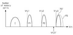
도 2는 프로그램 동작에 따라 메모리 셀들의 문턱 전압들이 형성되는 예를 보여준다. 도 2에서, 가로 축은 메모리 셀들의 문턱 전압(Vth)을 가리키고, 세로 축은 메모리 셀들의 수를 가리킨다. 즉, 도 2에 프로그램 동작이 수행된 메모리 셀들의 문턱 전압 산포들이 도시된다. 도 2는 예시적으로 2비트의 정보를 저장하는 MLC의 문턱 전압 산포를 보여준다.2 shows an example in which threshold voltages of memory cells are formed according to a program operation. In FIG. 2 , the horizontal axis indicates threshold voltages (Vth) of memory cells, and the vertical axis indicates the number of memory cells. That is, threshold voltage distributions of memory cells on which a program operation has been performed are shown in FIG. 2 . FIG. 2 exemplarily shows a threshold voltage distribution of an MLC storing 2 bits of information.
도 2를 참조하면, 메모리 셀들은 프로그램 동작이 수행됨에 따라 소거 상태(E), 제 1 프로그램 상태(P1), 제 2 프로그램 상태(P2), 및 제 3 프로그램 상태(P3)를 가질 수 있다. 메모리 셀들은 복수의 프로그램 루프들을 통해 대응하는 프로그램 상태의 문턱 전압을 가질 수 있다.Referring to FIG. 2 , as a program operation is performed, memory cells may have an erase state (E), a first program state (P1), a second program state (P2), and a third program state (P3). Memory cells may have threshold voltages in a corresponding program state through a plurality of program loops.
메모리 셀들은 ISPP(Incremental Step Pulse Programming) 방식에 따라 프로그램될 수 있다. ISPP 방식에 의해 프로그램되는 경우, 프로그램 루프가 진행됨에 따라 프로그램 전압은 상승한다. 메모리 셀들의 셀-스피드(Cell-speed)는 각각 다를 수 있다. 메모리 셀의 셀-스피드(Cell-speed)는 프로그램 전압을 인가한 후 메모리 셀의 문턱 전압의 상승 정도를 의미한다. 예를 들면, 낮은 프로그램 전압을 인가 시 검증 패스되는 메모리 셀은 셀-스피드가 빠르다. 높은 프로그램 전압을 인가 시 검증 패스되는 메모리 셀은 셀-스피드가 느리다. 하지만, 셀-스피드가 빠른 메모리 셀은 낮은 프로그램 전압 인가 시 검증 패스되기 때문에 프로그램 상태의 문턱 전압 산포에서 낮은 문턱 전압을 가진다. 셀-스피드가 빠른 메모리 셀은 높은 프로그램 전압 인가 시 검증 패스되기 때문에 프로그램 상태의 문턱 전압 산포에서 높은 문턱 전압을 가진다.Memory cells may be programmed according to an incremental step pulse programming (ISPP) method. In the case of programming using the ISPP method, the program voltage rises as the program loop progresses. Cell-speeds of memory cells may be different. The cell-speed of a memory cell refers to an increase in a threshold voltage of a memory cell after a program voltage is applied. For example, a memory cell that passes verification when a low program voltage is applied has a high cell-speed. A memory cell that passes verification when a high program voltage is applied has a low cell-speed. However, since a memory cell having a high cell-speed passes verification when a low program voltage is applied, it has a low threshold voltage in a threshold voltage distribution in a programmed state. A memory cell with a high cell-speed has a high threshold voltage in a threshold voltage distribution in a programmed state because the verification pass occurs when a high program voltage is applied.
도 2에서, 제 3 검증 전압(Vfy3)으로 검증 동작을 수행하는 경우, 제 3 프로그램 상태(P3)는 점선으로 도시된 문턱 전압 산포를 가질 수 있다. 이때 제 3 프로그램 상태에 대하여 검증 전압을 제 3' 검증 전압(Vfy3')으로 변경하여 검증 동작을 수행하면, 문턱 전압 산포는 제 3' 프로그램 상태(P3')의 산포를 가질 수 있다. 따라서, 제 3 프로그램 상태(P3)의 문턱 전압 산포는 개선될 수 있다. 도 2에서는 제 3 프로그램 상태(P3)에 대하여 예시적으로 설명되었지만, 다른 프로그램 상태들(P1, P2)에도 이러한 산포 개선은 동일하게 적용될 수 있다.In FIG. 2 , when the verification operation is performed with the third verification voltage Vfy3, the third program state P3 may have a threshold voltage distribution indicated by a dotted line. At this time, if the verification operation is performed by changing the verification voltage to the 3' verification voltage (Vfy3') for the third program state, the threshold voltage distribution may have a distribution of the 3' program state (P3'). Accordingly, the threshold voltage distribution of the third program state P3 may be improved. Although the third program state P3 is exemplarily described in FIG. 2 , the distribution improvement may be equally applied to the other program states P1 and P2.
도 3은 본 발명의 실시 예에 따른 불휘발성 메모리 장치의 프로그램 방법을 보여주는 도면이다. 도 3을 참조하면, 메모리 셀들은 복수의 프로그램 루프(Loop1~Loop4)를 통하여 프로그램 될 수 있다. 프로그램 루프 카운트가 증가할수록 프로그램 전압들(Vpgm1~Vpgm4)은 증가할 수 있다. 도 3에서는 예시적으로 제 4 프로그램 루프(Loop4)까지 도시되었으나, 프로그램 루프의 수는 더 많을 수 있다.3 is a diagram illustrating a programming method of a nonvolatile memory device according to an embodiment of the present invention. Referring to FIG. 3 , memory cells may be programmed through a plurality of program loops (Loop1 to Loop4). As the program loop count increases, the program voltages Vpgm1 to Vpgm4 may increase. In FIG. 3, up to the fourth program loop (Loop4) is illustratively shown, but the number of program loops may be greater.
불휘발성 메모리 장치(100)는 제 1 프로그램 루프(Loop1)에서 제 3 검증 전압(Vfy3)에 대응하는 메모리 셀들의 프로그램 패스/페일을 카운트할 수 있다. 불휘발성 메모리 장치(100)는 메모리 셀들의 프로그램 패스/페일 카운트 결과에 기초하여 제 3 검증 전압(Vfy3)을 변경할 오프셋 시점(Offset Point)을 결정할 수 있다. 예를 들면, 불휘발성 메모리 장치(100)는 제 3 검증 전압(Vfy3)에 대응하는 오프-셀들의 수를 계산할 수 있다. 불휘발성 메모리 장치(100)는 계산된 오프-셀들의 수를 소정의 기준 값들과 비교할 수 있다. 불휘발성 메모리 장치(100)는 계산된 오프-셀들의 수와 기준 값의 비교 결과에 따라 오프셋 시점을 제 3 프로그램 루프(Loop3)로 결정할 수 있다.The
불휘발성 메모리 장치(100)는 오프셋 시점(Loop3)에 검증 전압을 변경할 수 있다. 예를 들면, 제 3 프로그램 상태에 대응하는 제 3 검증 전압(Vfy3)은 제 3' 검증 전압(Vfy3')으로 변경될 수 있다. 이때 오프셋 전압은 ΔVfy이다. 검증 전압은 오프셋 전압만큼 감소할 수 있다. 오프셋 시점 이후에, 검증 전압은 단계적으로 감소할 수 있다. 하지만, 검증 전압의 감소 방법은 이것에 한정되지 않는다. 검증 전압은 복수의 오프셋 전압들의 사용하여 감소할 수 있다. 검증 전압은 한번만 변경된 후 유지될 수 있다.The
도 4는 도 3의 검증 전압의 오프셋 시점을 적응적으로 결정하는 방법을 보여주는 도면이다. 도 4에서 가로 축은 프로그램 루프 횟수를 가리키고, 세로 축은 검증 전압의 레벨을 가리킨다. 도 4는 도 3의 제 3 검증 전압(Vfy3)을 예시적으로 보여준다. 따라서, 제 1 및 제 2 검증 전압들(Vfy1, Vfy2)도 유사한 방식으로 오프셋 시점을 결정할 수 있다.FIG. 4 is a diagram illustrating a method of adaptively determining an offset timing of the verification voltage of FIG. 3 . In FIG. 4 , the horizontal axis indicates the number of program loops, and the vertical axis indicates the level of the verification voltage. FIG. 4 exemplarily shows the third verification voltage Vfy3 of FIG. 3 . Accordingly, offset timings of the first and second verification voltages Vfy1 and Vfy2 may be determined in a similar manner.
불휘발성 메모리 장치(100)는 프로그램 루프 횟수가 증가할수록 프로그램 전압을 단계적으로 증가하여 인가할 수 있다. 프로그램 루프 횟수가 증가하여도 제 3 프로그램 전압(Vfy3)은 일정하게 유지된다. 오프셋 전압을 적용하지 않는다면, 제 3 프로그램 전압(Vfy3)은 모든 프로그램 루프에서 동일하게 유지될 것이다.The
불휘발성 메모리 장치(100)는 검증 레벨 오프셋 결정 시점(DP)에 제 3 검증 전압(Vfy3)에 대응하는 메모리 셀들의 프로그램 패스/페일을 카운트할 수 있다. 불휘발성 메모리 장치(100)는 프로그램 패스/페일의 카운트 결과에 따라 검증 전압을 변경할 오프셋 시점(OP1, OP2, OP3)을 결정할 수 있다. 예를 들면, 불휘발성 메모리 장치(100)는 검증 레벨 오프셋 결정 시점(DP)에 제 3 검증 전압(Vfy3)을 인가한 후 온-셀들 또는 오프-셀들의 수를 계산할 수 있다. 불휘발성 메모리 장치(100)는 온-셀들 또는 오프-셀들의 수를 소정의 기준 값들과 비교하여 오프셋 시점들(OP1, OP2, OP3) 중 하나를 선택할 수 있다.The
따라서, 불휘발성 메모리 장치(100)는 적응적으로 검증 전압의 오프셋 시점을 결정할 수 있다. 예를 들면, 불휘발성 메모리 장치(100)는 마모도(wear level), 주변 환경, 칩 간 특성 차이 등을 고려하여 검증 전압의 오프셋 시점을 적응적으로 결정할 수 있다.Accordingly, the
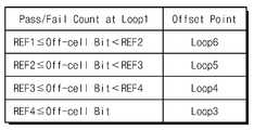
도 5는 도 3의 검증 전압의 오프셋 시점을 적응적으로 결정하는 방법을 예시적으로 보여주는 표이다. 도 5를 참조하면, 불휘발성 메모리 장치(100)는 제 1 프로그램 루프(Loop1)에서 제 3 프로그램 상태(P3)의 메모리 셀들의 패스/페일 카운트를 수행할 수 있다. 예를 들면, 불휘발성 메모리 장치(100)는 제 1 프로그램 루프(Loop1)에서 제 3 검증 전압(Vfy3)을 인가하여 오프-셀들의 비트 수(Off-cell Bit)를 계산할 수 있다.FIG. 5 is a table exemplarily illustrating a method of adaptively determining an offset timing of the verification voltage of FIG. 3 . Referring to FIG. 5 , the
불휘발성 메모리 장치(100)는 오프-셀들의 비트 수가 작을수록 오프셋 시점을 더 늦은 시점으로 결정할 수 있다. 예를 들면, 오프-셀들의 비트 수가 제 1 기준 값(REF1)보다 크거나 같고 제 2 기준 값(REF2)보다 작은 경우, 불휘발성 메모리 장치(100)는 제 6 프로그램 루프(Loop6)를 오프셋 시점으로 결정할 수 있다. 오프-셀들의 비트 수가 제 2 기준 값(REF2)보다 크거나 같고 제 3 기준 값(REF3)보다 작은 경우, 불휘발성 메모리 장치(100)는 제 5 프로그램 루프(Loop5)를 오프셋 시점으로 결정할 수 있다. 오프-셀들의 비트 수가 제 3 기준 값(REF3)보다 크거나 같고 제 4 기준 값(REF4)보다 작은 경우, 불휘발성 메모리 장치(100)는 제 4 프로그램 루프(Loop4)를 오프셋 시점으로 결정할 수 있다. 오프-셀들의 비트 수가 제 4 기준 값(REF4)보다 크거나 같은 경우, 불휘발성 메모리 장치(100)는 제 3 프로그램 루프(Loop3)를 오프셋 시점으로 결정할 수 있다.The
도 6은 본 발명의 다른 실시 예에 따른 불휘발성 메모리 장치의 프로그램 방법을 보여주는 도면이다. 도 6을 참조하면, 메모리 셀들은 복수의 프로그램 루프(Loop1~Loop4)를 통하여 프로그램 될 수 있다. 프로그램 루프 카운트가 증가할수록 프로그램 전압들(Vpgm1~Vpgm4)은 증가할 수 있다. 도 6에서는 예시적으로 제 4 프로그램 루프(Loop4)까지 도시되었으나, 프로그램 루프의 수는 더 많을 수 있다.6 is a diagram illustrating a programming method of a nonvolatile memory device according to another embodiment of the present invention. Referring to FIG. 6 , memory cells may be programmed through a plurality of program loops (Loop1 to Loop4). As the program loop count increases, the program voltages Vpgm1 to Vpgm4 may increase. In FIG. 6, up to the fourth program loop (Loop4) is shown as an example, but the number of program loops may be greater.
불휘발성 메모리 장치(100)는 제 2 프로그램 루프(Loop2)에서 제 2 프로그램 상태(P2)에 대응하는 메모리 셀들의 프로그램 완료 여부를 확인할 수 있다. 불휘발성 메모리 장치(100)는 제 2 프로그램 상태(P2)에 대응하는 메모리 셀들의 프로그램 완료 여부 결과에 기초하여 제 3 검증 전압(Vfy3)을 변경할 오프셋 시점(Offset Point)을 결정할 수 있다. 예를 들면, 제 2 프로그램 상태(P2)에 대응하는 메모리 셀들의 프로그램이 완료된 경우, 불휘발성 메모리 장치(100)는 제 3 프로그램 루프(Loop3)를 오프셋 시점으로 결정할 수 있다.The
불휘발성 메모리 장치(100)는 오프셋 시점(Loop3)에 검증 전압을 변경할 수 있다. 예를 들면, 제 3 프로그램 상태에 대응하는 제 3 검증 전압(Vfy3)은 제 3' 검증 전압(Vfy3')으로 변경될 수 있다. 이때 오프셋 전압은 ΔVfy이다. 검증 전압은 오프셋 전압만큼 감소할 수 있다. 오프셋 시점 이후에, 검증 전압은 단계적으로 감소할 수 있다. 하지만, 검증 전압의 감소 방법은 이것에 한정되지 않는다. 검증 전압은 복수의 오프셋 전압들의 사용하여 감소할 수 있다. 검증 전압은 한번만 변경된 후 유지될 수 있다.The
도 7은 본 발명의 실시 예에 따른 검증 전압의 오프셋 시점을 적응적으로 결정하는 방법을 보여주는 순서도이다. 도 7을 참조하면, 불휘발성 메모리 장치(100)는 메모리 셀들의 셀 스피드에 기초하여 검증 전압에 오프셋 전압을 적용하는 시점을 적응적으로 제어할 수 있다.7 is a flowchart illustrating a method of adaptively determining an offset timing of a verification voltage according to an embodiment of the present invention. Referring to FIG. 7 , the
S110 단계에서, 불휘발성 메모리 장치(100)는 프로그램 요청을 수신할 수 있다. 예를 들면, 제어 로직(150)은 프로그램 명령에 대응하는 제어 신호(CTRL)를 수신할 수 있다. 입출력 회로(140)는 프로그램 될 데이터(DATA)를 수신할 수 있다.In step S110, the
S120 단계에서, 불휘발성 메모리 장치(100)는 수신된 데이터(DATA)에 따라 프로그램 루프들을 수행할 수 있다. 예를 들면, 불휘발성 메모리 장치(100)는 ISPP 방식에 기초하여 프로그램 루프 횟수가 증가할수록 프로그램 전압을 증가시킬 수 있다. 불휘발성 메모리 장치(100)는 적어도 하나의 프로그램 루프 동안에는 동일한 검증 전압을 사용할 수 있다.In step S120, the
S130 단계에서, 불휘발성 메모리 장치(100)는 특정 프로그램 루프에서 검증 동작에 따라 오프-셀들의 수를 카운트할 수 있다. 예를 들면, 패스/페일 카운터(151)는 특정 프로그램 루프에서 검증 전압을 인가한 후 검증 전압에 대응하는 오프-셀들의 수를 카운트할 수 있다.In step S130, the
S140 단계에서, 불휘발성 메모리 장치(100)는 S130 단계에서 측정된 오프-셀들의 카운팅 결과에 기초하여 검증 전압의 오프셋 시점을 결정할 수 있다. 예를 들면, 검증 레벨 오프셋 시점 제어기(152)는 측정된 오프-셀들의 수를 기준 값과 비교할 수 있다. 또한, 검증 레벨 오프셋 시점 제어기(152)는 복수의 기준 값들을 사용하여 검증 전압의 오프셋 시점을 결정할 수 있다. 오프셋 시점은 오프셋 시점을 결정한 프로그램 루프의 바로 다음 프로그램 루프일 수 있다. 또는 오프셋 시점은 오프셋 시점을 결정한 프로그램 루프로부터 특정 횟수의 프로그램 루프들 이후의 프로그램 루프일 수 있다. 즉, 불휘발성 메모리 장치(100)는 S130 단계에서 측정된 오프-셀들의 수에 기초하여 적응적으로 검증 전압에 오프셋 전압을 적용하는 시점을 결정할 수 있다. 또한, 오프셋 시점을 결정하는 프로그램 루프는 프로그램 동작의 가장 첫 번째 프로그램 루프일 수 있다. 또는 오프셋 시점을 결정하는 프로그램 루프는 프로그램 동작을 시작한 후 특정 횟수의 프로그램 루프들 이후의 프로그램 루프일 수 있다.In step S140 , the
S150 단계에서, 불휘발성 메모리 장치(100)는 프로그램 루프들을 수행할 수 있다. 예를 들면, 불휘발성 메모리 장치(100)는 S120 단계와 동일한 검증 전압을 이용하여 적어도 하나의 프로그램 루프를 수행할 수 있다. 또는 오프셋 시점이 오프셋 시점을 결정한 프로그램 루프의 바로 다음 프로그램 루프인 경우, S150 단계는 생략될 수 있다.In step S150, the
S160 단계에서, 불휘발성 메모리 장치(100)는 검증 전압의 오프셋 시점에 검증 전압을 변경하여 프로그램 루프를 수행할 수 있다. 예를 들면, 불휘발성 메모리 장치(100)는 S140 단계에서 결정된 프로그램 루프에 도달하면 검증 전압에 오프셋 전압을 적용하여 검증 동작을 수행할 수 있다. 따라서, 불휘발성 메모리 장치(100)는 도 2에서 설명된 효과에 따라 메모리 셀들의 산포를 개선할 수 있다.In step S160 , the
도 8은 도 1의 메모리 셀 어레이(110)의 메모리 블록들 중 하나(BLKi)를 보여주는 회로도이다. 도 8을 참조하면, 메모리 블록(BLKi)은 3차원 구조를 가질 수 있다. 예를 들면, 제 1 비트 라인(BL1) 및 공통 소스 라인(CSL) 사이에 낸드 스트링들(NS11~NS31)이 제공될 수 있다. 제 2 비트 라인(BL2) 및 공통 소스 라인(CSL) 사이에 낸드 스트링들(NS12, NS22, NS32)이 제공될 수 있다. 제 3 비트 라인(BL3) 및 공통 소스 라인(CSL) 사이에, 낸드 스트링들(NS13, NS23. NS33)이 제공될 수 있다.FIG. 8 is a circuit diagram showing one of the memory blocks BLKi of the
각 낸드 스트링(NS)은 스트링 선택 트랜지스터(SST), 접지 선택 트랜지스터(GST), 그리고 스트링 선택 트랜지스터(SST) 및 접지 선택 트랜지스터(GST) 사이에 연결된 복수의 메모리 셀들(MC)을 포함할 수 있다. 각 낸드 스트링(NS)의 스트링 선택 트랜지스터(SST)는 대응하는 비트 라인(BL)과 연결될 수 있다. 각 낸드 스트링(NS)의 접지 선택 트랜지스터(GST)는 공통 소스 라인(CSL)과 연결될 수 있다.Each NAND string NS may include a string select transistor SST, a ground select transistor GST, and a plurality of memory cells MC connected between the string select transistor SST and the ground select transistor GST. . The string select transistor SST of each NAND string NS may be connected to a corresponding bit line BL. The ground select transistor GST of each NAND string NS may be connected to the common source line CSL.
이하에서, 행 및 열 단위로 낸드 스트링들(NS)을 정의한다. 하나의 비트 라인(BL)에 공통으로 연결된 낸드 스트링들(NS)은 하나의 열을 형성한다. 예를 들면, 제 1 비트 라인(BL1)에 연결된 낸드 스트링들(NS11~NS31)은 제 1 열에 대응할 것이다. 제 2 비트 라인(BL2)에 연결된 낸드 스트링들(NS12~NS32)은 제 2 열에 대응할 것이다. 제 3 비트 라인(BL3)에 연결된 낸드 스트링들(NS13~NS33)은 제 3 열에 대응할 것이다.Hereinafter, NAND strings NS are defined in units of rows and columns. NAND strings NS commonly connected to one bit line BL form one column. For example, the NAND strings NS11 to NS31 connected to the first bit line BL1 may correspond to the first column. The NAND strings NS12 to NS32 connected to the second bit line BL2 correspond to the second column. The NAND strings NS13 to NS33 connected to the third bit line BL3 correspond to the third column.
하나의 스트링 선택 라인(SSL)에 연결되는 낸드 스트링들(NS)은 하나의 행을 형성한다. 예를 들면, 제 1 스트링 선택 라인(SSL1)에 연결된 낸드 스트링들(NS11~NS13)은 제 1 행을 형성한다. 제 2 스트링 선택 라인(SSL2)에 연결된 낸드 스트링들(NS21~NS23)은 제 2 행을 형성한다. 제 3 스트링 선택 라인(SSL3)에 연결된 낸드 스트링들(NS31~NS33)은 제 3 행을 형성한다.NAND strings NS connected to one string select line SSL form one row. For example, the NAND strings NS11 to NS13 connected to the first string selection line SSL1 form a first row. The NAND strings NS21 to NS23 connected to the second string select line SSL2 form a second row. The NAND strings NS31 to NS33 connected to the third string select line SSL3 form a third row.
각 낸드 스트링(NS)에서, 높이가 정의된다. 예시적으로, 각 낸드 스트링(NS)에서, 접지 선택 트랜지스터(GST)에 인접한 메모리 셀(MC1)의 높이는 1이다. 각 낸드 스트링(NS)에서, 스트링 선택 트랜지스터(SST)에 인접할수록 메모리 셀의 높이는 증가한다. 각 낸드 스트링(NS)에서, 스트링 선택 트랜지스터(SST)에 인접한 메모리 셀(MC7)의 높이는 7이다.In each NAND string NS, a height is defined. Exemplarily, in each NAND string NS, the height of the memory cell MC1 adjacent to the ground select transistor GST is 1. In each NAND string NS, the height of a memory cell increases as it is closer to the string select transistor SST. In each NAND string NS, the height of the memory cell MC7 adjacent to the string select transistor SST is 7.
동일한 행의 낸드 스트링들(NS)은 스트링 선택 라인(SSL)을 공유한다. 상이한 행의 낸드 스트링들(NS)은 상이한 스트링 선택 라인(SSL)에 연결된다. 낸드 스트링들(NS11~NS13, NS21~NS22, NS31~NS33)은 접지 선택 라인(GSL)을 공유한다. 동일한 행의 낸드 스트링들(NS)의 동일한 높이의 메모리 셀들은 워드 라인을 공유한다. 동일한 높이에서, 상이한 행의 낸드 스트링들(NS)의 워드 라인들(WL)은 공통으로 연결된다. 공통 소스 라인(CSL)은 낸드 스트링들(NS)에 공통으로 연결된다.NAND strings NS in the same row share a string select line SSL. NAND strings NS of different rows are connected to different string select lines SSL. The NAND strings NS11 to NS13, NS21 to NS22, and NS31 to NS33 share the ground select line GSL. Memory cells of the same height of the NAND strings NS in the same row share a word line. At the same height, word lines WL of NAND strings NS of different rows are connected in common. The common source line CSL is commonly connected to the NAND strings NS.
도 8에 도시된 바와 같이, 동일 높이의 워드 라인들(WL)은 공통으로 연결되어 있다. 따라서, 특정 워드 라인(WL)이 선택될 때, 특정 워드 라인(WL)에 연결된 모든 낸드 스트링들(NS)이 선택될 것이다. 상이한 행의 낸드 스트링들(NS)은 상이한 스트링 선택 라인(SSL)에 연결되어 있다. 따라서, 스트링 선택 라인들(SSL1~SSL3)을 선택함으로써, 동일 워드 라인(WL)에 연결된 낸드 스트링들(NS) 중 비선택 행의 낸드 스트링들(NS)이 비트 라인들(BL1~BL3)로부터 분리될 수 있다. 즉, 스트링 선택 라인들(SSL1~SSL3)을 선택함으로써, 낸드 스트링들(NS)의 행이 선택될 수 있다. 그리고 비트 라인들(BL1~BL3)을 선택함으로써, 선택 행의 낸드 스트링들(NS)이 열 단위로 선택될 수 있다.As shown in FIG. 8 , word lines WL having the same height are connected in common. Accordingly, when a specific word line WL is selected, all NAND strings NS connected to the specific word line WL will be selected. NAND strings NS of different rows are connected to different string select lines SSL. Therefore, by selecting the string select lines SSL1 to SSL3, NAND strings NS of an unselected row among the NAND strings NS connected to the same word line WL are selected from the bit lines BL1 to BL3. can be separated That is, a row of the NAND strings NS can be selected by selecting the string selection lines SSL1 to SSL3 . Also, by selecting the bit lines BL1 to BL3, the NAND strings NS of the selected row may be selected in units of columns.
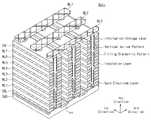
도 9는 도 8의 메모리 블록(BLKi)에 대응하는 구조의 실시 예를 보여주는 사시도이다. 도 9를 참조하면, 메모리 블록(BLKi)은 기판(SUB)과 수직 방향으로 형성될 수 있다. 기판(SUB)에는 n+ 도핑 영역이 형성될 수 있다.FIG. 9 is a perspective view illustrating an embodiment of a structure corresponding to the memory block BLKi of FIG. 8 . Referring to FIG. 9 , the memory block BLKi may be formed in a direction perpendicular to the substrate SUB. An n+ doped region may be formed on the substrate SUB.
기판(SUB) 위에는 게이트 전극막(gate electrode layer)과 절연막(insulation layer)이 교대로 증착될 수 있다. 게이트 전극막(gate electrode layer)과 절연막(insulation layer) 사이에는 정보 저장막(information storage layer)이 형성될 수 있다. 게이트 전극막과 절연막을 수직 방향으로 패터닝(vertical patterning)하면, V자 모양의 필라(pillar)가 형성될 수 있다. 필라는 게이트 전극막과 절연막을 관통하여 기판(SUB)과 연결될 수 있다. 필라(pillar)의 내부는 충전 유전 패턴(filling dielectric pattern)으로 실리콘 산화물(Silicon Oxide)과 같은 절연 물질로 구성될 수 있다. 필라의 외부는 수직 활성 패턴(vertical active pattern)으로 채널 반도체로 구성될 수 있다.A gate electrode layer and an insulation layer may be alternately deposited on the substrate SUB. An information storage layer may be formed between the gate electrode layer and the insulation layer. When the gate electrode layer and the insulating layer are vertically patterned, a V-shaped pillar may be formed. The pillar may be connected to the substrate SUB by penetrating the gate electrode layer and the insulating layer. The inside of the pillar may be made of an insulating material such as silicon oxide as a filling dielectric pattern. The outside of the pillar may be composed of a channel semiconductor with a vertical active pattern.
메모리 블록(BLKi)의 게이트 전극막(gate electrode layer)은 접지 선택 라인(GSL), 복수의 워드 라인들(WL1 ~ WL7), 그리고 스트링 선택 라인(SSL)에 연결될 수 있다. 그리고 메모리 블록(BLKi)의 필라(pillar)는 복수의 비트 라인들(BL1 ~ BL3)과 연결될 수 있다. 도 8에서는, 하나의 메모리 블록(BLKi)이 2개의 선택 라인(GSL, SSL), 7개의 워드 라인(WL1 ~ WL7), 그리고 3개의 비트 라인(BL1 ~ BL3)을 갖는 것으로 도시되어 있으나, 실제로는 이것들보다 더 많거나 적을 수 있다.A gate electrode layer of the memory block BLKi may be connected to a ground selection line GSL, a plurality of word lines WL1 to WL7, and a string selection line SSL. Also, a pillar of the memory block BLKi may be connected to a plurality of bit lines BL1 to BL3. In FIG. 8 , one memory block BLKi is illustrated as having two select lines GSL and SSL, seven word lines WL1 to WL7, and three bit lines BL1 to BL3, but actually may be more or less than these.
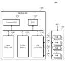
도 10은 본 발명의 실시 예에 따른 솔리드 스테이트 드라이브(Soild State Drive, 이하 SSD)를 예시적으로 보여주는 블록도이다. 도 10을 참조하면, SSD(1000)는 복수의 불휘발성 메모리 장치들(1100) 및 SSD 제어기(1200)를 포함할 수 있다.10 is a block diagram exemplarily showing a solid state drive (SSD) according to an embodiment of the present invention. Referring to FIG. 10 , an
불휘발성 메모리 장치들(1100)은 선택적으로 외부 고전압(VPPx)을 제공받도록 구현될 수 있다. 불휘발성 메모리 장치들(1100) 각각은 도 1 내지 도 9에서 설명된 바와 같이 메모리 셀들의 프로그램 속도에 기초하여 검증 전압의 오프셋 적용 시점을 적응적으로 결정하여 메모리 셀들의 산포를 개선할 수 있다.The
SSD 제어기(1200)는 복수의 채널들(CH1 ~ CHi, i는 2 이상의 정수)을 통하여 불휘발성 메모리 장치들(1100)에 연결될 수 있다. SSD 제어기(1200)는 적어도 하나의 프로세서(1210), 버퍼 메모리(1220), 에러 정정 회로(1230), 호스트 인터페이스(1240) 및 불휘발성 메모리 인터페이스(1250)를 포함할 수 있다.The
버퍼 메모리(1220)는 메모리 제어기(1200)의 구동에 필요한 데이터를 임시로 저장할 것이다. 버퍼 메모리(1220)는 데이터 혹은 명령을 저장하는 복수의 메모리 라인들을 포함할 수 있다.The
에러 정정 회로(1230)는 쓰기 동작에서 프로그램될 데이터의 에러 정정 코드 값을 계산하고, 읽기 동작에서 읽혀진 데이터를 에러 정정 코드 값에 근거로 하여 에러 정정하고, 데이터 복구 동작에서 불휘발성 메모리 장치(1100)로부터 복구된 데이터의 에러를 정정할 수 있다. 도시되지 않았지만, 메모리 제어기(1200)를 구동하는 데 필요한 코드 데이터를 저장하는 코드 메모리가 더 포함될 수 있다. 코드 메모리는 불휘발성 메모리 장치로 구현될 수 있다.The
호스트 인터페이스(1240)는 외부의 장치와 인터페이스 기능을 제공할 수 있다. 여기서 호스트 인터페이스(1240)는 낸드 인터페이스일 수 있다. 불휘발성 메모리 인터페이스(1250)는 불휘발성 메모리 장치(1100)와 인터페이스 기능을 제공할 수 있다.The
도 11은 본 발명의 실시 예에 따른 eMMC를 예시적으로 보여주는 블록도이다. 도 11을 참조하면, eMMC(2000)는 적어도 하나의 낸드 플래시 메모리 장치(2100) 및 제어기(2200)를 포함할 수 있다.11 is a block diagram exemplarily showing an eMMC according to an embodiment of the present invention. Referring to FIG. 11 , an
낸드 플래시 메모리 장치(2100)는 SDR(Single Data Rate) 낸드 혹은 DDR(Double Data Rate) 낸드일 수 있다. 혹은 낸드 플래시 메모리 장치(2100)는 수직형 낸드 플래시 메모리 장치(Vertical NAND; VNAND)일 수 있다. 낸드 플래시 메모리 장치(2100)는 도 1 내지 도 9에서 설명된 바와 같이 메모리 셀들의 프로그램 속도에 기초하여 검증 전압의 오프셋 적용 시점을 적응적으로 결정하여 메모리 셀들의 산포를 개선할 수 있다.The NAND
제어기(2200)는 복수의 채널들을 통하여 낸드 플래시 메모리 장치(2100)에 연결될 수 있다. 제어기(2200)는 적어도 하나의 제어기 코어(2210), 호스트 인터페이스(2240) 및 낸드 인터페이스(2250)를 포함할 수 있다. 적어도 하나의 제어기 코어(2210)는 eMMC(2000)의 전반적인 동작을 제어할 수 있다. 호스트 인터페이스(2240)는 제어기(2210)와 호스트의 인터페이싱을 수행할 수 있다. 낸드 인터페이스(2250)는 낸드 플래시 메모리 장치(2100)와 제어기(2200)의 인터페이싱을 수행한다. 실시 예에 있어서, 호스트 인터페이스(2240)는 병렬 인터페이스(예를 들어, MMC 인터페이스)일 수 있다. 다른 실시 예에 있어서, eMMC(2000)의 호스트 인터페이스(2240)는 직렬 인터페이스(예를 들어, UHS-II, UFS 인터페이스)일 수 있다.The
eMMC(2000)는 호스트로부터 전원 전압들(Vcc, Vccq)을 제공받을 수 있다. 여기서, 제 1 전원 전압(Vcc, 예를 들어 3.3V)은 낸드 플래시 메모리 장치(2100) 및 낸드 인터페이스(2250)에 제공되고, 제 2 전원 전압(Vccq, 예를 들어 1.8V/3.3V)은 제어기(2200)에 제공될 수 있다. 실시 예에 있어서, eMMC(2000)는 외부 고전압(VPPx)을 선택적으로 제공받을 수 있다.The
본 발명은 UFS(Universal Flash Storage) 시스템에도 적용 가능하다. 도 12는 본 발명의 실시 예에 따른 UFS 시스템을 예시적으로 보여주는 블록도이다. 도 12를 참조하면, UFS 시스템(3000)은 UFS 호스트(3100)와 UFS 장치(3200)를 포함할 수 있다.The present invention is also applicable to Universal Flash Storage (UFS) systems. 12 is a block diagram exemplarily showing a UFS system according to an embodiment of the present invention. Referring to FIG. 12 , a
UFS 호스트(3100)는 애플리케이션(3110), 장치 드라이버(3120), 호스트 컨트롤러(3130), 그리고 버퍼 램(3140)을 포함할 수 있다. 그리고 호스트 컨트롤러(3130)는 커맨드 큐(CMD queue, 3131), 호스트 DMA(3132), 그리고 전원 관리자(3133)를 포함할 수 있다. 커맨드 큐(3131), 호스트 DMA(3132), 그리고 전원 관리자(3133)는 호스트 컨트롤러(3130) 내에서 알고리즘, 소프트웨어, 또는 펌웨어로 동작할 수 있다.The
UFS 호스트(3100)의 애플리케이션(3110)과 장치 드라이버(3120)에서 생성된 커맨드(예를 들면, 쓰기 커맨드)는 호스트 컨트롤러(3130)의 커맨드 큐(3131)에 입력될 수 있다. 커맨드 큐(3131)는 UFS 장치(3200)로 제공될 커맨드를 순서대로 저장할 수 있다. 커맨드 큐(3131)에 저장된 커맨드는 호스트 DMA(3132)로 제공될 수 있다. 호스트 DMA(3132)는 커맨드를 호스트 인터페이스(3101)를 통해 UFS 장치(3200)로 보낸다.A command (eg, a write command) generated by the
계속해서 도 12를 참조하면, UFS 장치(3200)는 플래시 메모리(3210), 장치 컨트롤러(3230), 그리고 버퍼 램(3240)을 포함할 수 있다. 그리고 장치 컨트롤러(3230)는 중앙처리장치(CPU, 3231), 커맨드 관리자(CMD manager, 3232), 플래시 DMA(3233), 보안 관리자(security manager, 3234), 버퍼 관리자(3235), 플래시 변환 계층(FTL; Flash Translation Layer, 3236), 그리고 플래시 관리자(3237)를 포함할 수 있다. 여기에서, 커맨드 관리자(3232), 보안 관리자(3234), 버퍼 관리자(3235), 플래시 변환 계층(3236), 그리고 플래시 관리자(3237)는 장치 컨트롤러(3230) 내에서 알고리즘, 소프트웨어, 또는 펌웨어로 동작할 수 있다.Continuing to refer to FIG. 12 , the
플래시 메모리(3210)는 도 1 내지 도 9에서 설명된 바와 같이 메모리 셀들의 프로그램 속도에 기초하여 검증 전압의 오프셋 적용 시점을 적응적으로 결정하여 메모리 셀들의 산포를 개선할 수 있다.As described with reference to FIGS. 1 to 9 , the
UFS 호스트(3100)로부터 UFS 장치(3200)로 입력된 커맨드는 장치 인터페이스(3201)를 통해 커맨드 관리자(3232)로 제공될 수 있다. 커맨드 관리자(3232)는 UFS 호스트(3100)로부터 제공된 커맨드를 해석하고, 보안 관리자(3234)를 이용하여 입력된 커맨드를 인증할 수 있다. 커맨드 관리자(3232)는 버퍼 관리자(3235)를 통해 데이터를 입력받을 수 있도록 버퍼 램(3240)을 할당할 수 있다. 커맨드 관리자(3232)는 데이터 전송 준비가 완료되면, UFS 호스트(3100)로 RTT(READY_TO_TRANSFER) UPIU를 보낸다.A command input from the
UFS 호스트(3100)는 RTT UPIU에 응답하여 데이터를 UFS 장치(3200)로 전송할 수 있다. 데이터는 호스트 DMA(3132)와 호스트 인터페이스(3101)를 통해 UFS 장치(3200)로 전송될 수 있다. UFS 장치(3200)는 제공받은 데이터를 버퍼 관리자(3235)를 통해 버퍼 램(3240)에 저장할 수 있다. 버퍼 램(3240)에 저장된 데이터는 플래시 DMA(3233)를 통해 플래시 관리자(3237)로 제공될 수 있다. 플래시 관리자(3237)는 플래시 변환 계층(3236)의 어드레스 맵핑 정보를 참조하여, 플래시 메모리(3210)의 선택된 어드레스에 데이터를 저장할 수 있다.The
UFS 장치(3200)는 커맨드에 필요한 데이터 전송과 프로그램이 완료되면, 인터페이스를 통해 UFS 호스트(3100)로 응답 신호(response)를 보내고, 커맨드 완료를 알린다. UFS 호스트(3100)는 응답 신호를 전달받은 커맨드에 대한 완료 여부를 장치 드라이버(3120)와 애플리케이션(3110)에 알려주고, 해당 커맨드에 대한 동작을 종료할 수 있다.When data transmission and programming required for a command are completed, the
본 발명은 모바일 장치에도 적용 가능하다. 도 13은 본 발명의 실시 예에 따른 모바일 장치를 예시적으로 보여주는 블록도이다. 도 13을 참조하면, 모바일 장치(4000)는 애플리케이션 프로세서(4100), 통신 모듈(4200), 디스플레이/터치 모듈(4300), 저장 장치(4400), 및 모바일 램(4500)을 포함할 수 있다.The present invention is also applicable to mobile devices. 13 is a block diagram showing a mobile device according to an embodiment of the present invention by way of example. Referring to FIG. 13 , a
애플리케이션 프로세서(4100)는 모바일 장치(4000)의 전반적인 동작을 제어할 수 있다. 통신 모듈(4200)은 외부와의 유선/무선 통신을 제어하도록 구현될 것이다. 디스플레이/터치 모듈(4300)은 애플리케이션 프로세서(4100)에서 처리된 데이터를 디스플레이 하거나, 터치 패널로부터 데이터를 입력 받도록 구현될 것이다. 저장 장치(4400)는 사용자의 데이터를 저장하도록 구현될 것이다. 저장 장치(4400)는 eMMC, SSD, UFS 장치일 수 있다. 모바일 램(4500)은 모바일 장치(4000)의 처리 동작 시 필요한 데이터를 임시로 저장하도록 구현될 수 있다.The
저장 장치(4400)는 도 1 내지 도 9에서 설명된 바와 같이 메모리 셀들의 프로그램 속도에 기초하여 검증 전압의 오프셋 적용 시점을 적응적으로 결정하여 메모리 셀들의 산포를 개선할 수 있다.As described with reference to FIGS. 1 to 9 , the
이상에서와 같이 도면과 명세서에서 실시 예가 개시되었다. 여기서 특정한 용어들이 사용되었으나, 이는 단지 본 발명을 설명하기 위한 목적에서 사용된 것이지 의미 한정이나 특허 청구범위에 기재된 본 발명의 범위를 제한하기 위하여 사용된 것은 아니다. 그러므로 본 기술분야의 통상의 지식을 가진 자라면 이로부터 다양한 변형 및 균등한 타 실시 예가 가능하다는 점을 이해할 것이다. 따라서 본 발명의 진정한 기술적 보호 범위는 첨부된 특허 청구범위의 기술적 사상에 의해 정해져야 할 것이다.As described above, embodiments have been disclosed in the drawings and specifications. Although specific terms have been used herein, they are only used for the purpose of describing the present invention and are not used to limit the scope of the present invention described in the claims. Therefore, those skilled in the art will understand that various modifications and equivalent other embodiments are possible therefrom. Therefore, the true technical protection scope of the present invention should be determined by the technical spirit of the appended claims.
100 : 불휘발성 메모리 장치
110 : 메모리 셀 어레이
120 : 어드레스 디코더
130 : 전압 발생기
140 : 입출력 회로
150 : 제어 로직
151 : 패스/페일 카운터
152 : 검증 레벨 오프셋 시점 제어기
1000 : SSD
2000 : eMMC
3000 : UFS 시스템
4000 : 모바일 장치100: non-volatile memory device
110: memory cell array
120: address decoder
130: voltage generator
140: input/output circuit
150: control logic
151: pass/fail counter
152: verification level offset timing controller
1000: SSD
2000: eMMC
3000: UFS system
4000: mobile device
Claims (10)
Translated fromKorean검증 동작 시 상기 메모리 셀들 중 선택된 메모리 셀들에 검증 전압을 제공하는 어드레스 디코더; 그리고
특정 시점 이후의 검증 동작에서 상기 검증 전압을 변경하도록 제어하는 제어 로직을 포함하되,
상기 제어 로직은:
제 1 프로그램 루프의 검증 동작의 결과에 기초하여 상기 제 1 프로그램 루프의 오프-셀들의 수를 카운트하는 패스-페일 카운터; 그리고
상기 제 1 프로그램 루프의 오프-셀들의 수와 적어도 하나의 기준 값을 비교하여 상기 검증 전압이 변경되는 제 2 프로그램 루프를 결정하고, 상기 제 2 프로그램 루프를 검증 전압 오프셋 시점으로 결정하는 검증 레벨 오프셋 시점 제어기를 포함하는 불휘발성 메모리 장치.a memory cell array including a plurality of memory cells;
an address decoder providing a verify voltage to selected memory cells among the memory cells during a verify operation; and
Including control logic for controlling the verification voltage to be changed in a verification operation after a specific point in time,
The control logic is:
a pass-fail counter counting the number of off-cells of the first program loop based on a result of a verify operation of the first program loop; and
A verification level offset determining a second program loop in which the verification voltage is changed by comparing the number of off-cells of the first program loop with at least one reference value, and determining the second program loop as a verification voltage offset time point A non-volatile memory device including a point-in-time controller.
상기 제 1 프로그램 루프의 오프-셀들의 수가 제 1 기준 값보다 크거나 같고 제 2 기준 값보다 작은 경우, 상기 제어 로직은 상기 제 1 프로그램 루프로부터 제 1 루프들 이후에 수행되는 상기 제 2 프로그램 루프를 상기 검증 전압 오프셋 시점으로 결정하는 불휘발성 메모리 장치.According to claim 1,
When the number of off-cells of the first program loop is greater than or equal to a first reference value and less than a second reference value, the control logic is performed in the second program loop performed after first loops from the first program loop. A nonvolatile memory device that determines the verification voltage offset time point.
상기 제 1 프로그램 루프의 오프-셀들의 수가 상기 제 2 기준 값보다 크거나 같은 경우, 상기 제어 로직은 상기 제 1 프로그램 루프로부터 상기 제 1 루프들보다 작은 제 2 루프들 이후에 수행되는 상기 제 2 프로그램 루프를 상기 검증 전압 오프셋 시점으로 결정하는 불휘발성 메모리 장치.According to claim 4,
When the number of off-cells in the first program loop is greater than or equal to the second reference value, the control logic is performed after second loops smaller than the first loops from the first program loop. A nonvolatile memory device for determining a program loop as the verification voltage offset timing.
상기 제어 로직은 상기 제 2 프로그램 루프에서 상기 검증 전압을 제 1 오프셋 전압만큼 감소시키는 불휘발성 메모리 장치.According to claim 1,
The control logic reduces the verification voltage by a first offset voltage in the second program loop.
상기 제어 로직은 상기 제 2 프로그램 루프의 다음 루프에서 상기 검증 전압을 상기 제 1 오프셋 전압의 두 배인 제 2 오프셋 전압만큼 감소시키는 불휘발성 메모리 장치.According to claim 6,
The control logic reduces the verification voltage by a second offset voltage that is twice the first offset voltage in a loop following the second program loop.
검증 동작 시 상기 메모리 셀들 중 선택된 메모리 셀들에 검증 전압을 제공하는 어드레스 디코더; 그리고
특정 시점 이후의 검증 동작에서 상기 검증 전압를 변경하도록 제어하는 제어 로직을 포함하되,
상기 제어 로직은:
제 1 프로그램 루프의 검증 동작 시 특정 프로그램 상태의 프로그램 완료 여부에 기초하여 상기 제 1 프로그램 루프의 오프-셀들의 수를 카운트하는 패스-페일 카운터; 그리고
상기 제 1 프로그램 루프의 오프-셀들의 수와 적어도 하나의 기준 값을 비교하여 상기 검증 전압이 변경되는 제 2 프로그램 루프를 결정하고, 상기 제 2 프로그램 루프를 검증 전압 오프셋 시점으로 결정하는 검증 레벨 오프셋 시점 제어기를 포함하는 불휘발성 메모리 장치.a memory cell array including a plurality of memory cells;
an address decoder providing a verify voltage to selected memory cells among the memory cells during a verify operation; and
Including control logic for controlling the verification voltage to be changed in a verification operation after a specific point in time,
The control logic is:
a pass-fail counter counting the number of off-cells of the first program loop based on whether a program in a specific program state is completed during a verification operation of the first program loop; and
A verification level offset determining a second program loop in which the verification voltage is changed by comparing the number of off-cells of the first program loop with at least one reference value, and determining the second program loop as a verification voltage offset time point A non-volatile memory device including a point-in-time controller.
상기 제어 로직은 상기 제 1 프로그램 루프의 검증 동작 시 제 1 프로그램 상태의 프로그램이 완료된 경우 상기 제 1 프로그램 루프의 바로 다음 루프를 상기 검증 전압 오프셋 시점으로 결정하는 불휘발성 메모리 장치.According to claim 8,
wherein the control logic determines a loop immediately following the first program loop as the verification voltage offset timing when a program in a first program state is completed during a verification operation of the first program loop.
상기 제어 로직은 상기 제 1 프로그램 루프의 검증 동작 시 제 1 프로그램 상태의 프로그램이 완료된 경우 상기 제 2 프로그램 루프에서 상기 제 1 프로그램 상태와 인접한 프로그램 상태에 대응하는 검증 전압을 변경하는 불휘발성 메모리 장치.According to claim 8,
wherein the control logic changes a verification voltage corresponding to a program state adjacent to the first program state in the second program loop when programming of the first program state is completed during the verification operation of the first program loop.
Priority Applications (3)
| Application Number | Priority Date | Filing Date | Title |
|---|---|---|---|
| KR1020150181882AKR102473167B1 (en) | 2015-12-18 | 2015-12-18 | Nonvolatile memory device and erasing method thereof |
| US15/381,724US9899097B2 (en) | 2015-12-18 | 2016-12-16 | Nonvolatile memory device and method of programming the same |
| CN201611168375.4ACN107017028B (en) | 2015-12-18 | 2016-12-16 | Non-volatile memory device and method of programming the same |
Applications Claiming Priority (1)
| Application Number | Priority Date | Filing Date | Title |
|---|---|---|---|
| KR1020150181882AKR102473167B1 (en) | 2015-12-18 | 2015-12-18 | Nonvolatile memory device and erasing method thereof |
Publications (2)
| Publication Number | Publication Date |
|---|---|
| KR20170073800A KR20170073800A (en) | 2017-06-29 |
| KR102473167B1true KR102473167B1 (en) | 2022-12-02 |
Family
ID=59066565
Family Applications (1)
| Application Number | Title | Priority Date | Filing Date |
|---|---|---|---|
| KR1020150181882AActiveKR102473167B1 (en) | 2015-12-18 | 2015-12-18 | Nonvolatile memory device and erasing method thereof |
Country Status (3)
| Country | Link |
|---|---|
| US (1) | US9899097B2 (en) |
| KR (1) | KR102473167B1 (en) |
| CN (1) | CN107017028B (en) |
Families Citing this family (17)
| Publication number | Priority date | Publication date | Assignee | Title |
|---|---|---|---|---|
| JP6683262B2 (en)* | 2016-11-02 | 2020-04-15 | 株式会社村田製作所 | Ceramic electronic component and method for manufacturing ceramic electronic component |
| US11158381B2 (en) | 2017-10-12 | 2021-10-26 | Samsung Electronics Co., Ltd. | Non-volatile memory device and operating method thereof |
| KR102336662B1 (en) | 2017-10-12 | 2021-12-07 | 삼성전자 주식회사 | Non-volatile memory device and method of operating the non-volatile memory device |
| KR102477267B1 (en)* | 2017-11-14 | 2022-12-13 | 삼성전자주식회사 | Nonvolatile memory device and operating method of the same |
| KR102504295B1 (en)* | 2017-11-24 | 2023-02-27 | 삼성전자 주식회사 | Nonvolatile Memory Device, and Programming Method Thereof |
| US10741256B2 (en)* | 2018-09-18 | 2020-08-11 | Western Digital Technologies, Inc. | Data storage systems and methods for improved recovery after a write abort event |
| KR102717016B1 (en)* | 2019-03-05 | 2024-10-15 | 에스케이하이닉스 주식회사 | Memory device and operating method thereof |
| CN111863100A (en)* | 2019-04-29 | 2020-10-30 | 北京兆易创新科技股份有限公司 | Programming method and device of nonvolatile memory |
| US10714198B1 (en)* | 2019-06-04 | 2020-07-14 | Sandisk Technologies Llc | Dynamic 1-tier scan for high performance 3D NAND |
| JP7360478B2 (en) | 2019-10-18 | 2023-10-12 | 長江存儲科技有限責任公司 | Memory device and method |
| KR102743817B1 (en)* | 2019-11-21 | 2024-12-18 | 에스케이하이닉스 주식회사 | Memory device and operating method thereof |
| KR102761245B1 (en)* | 2020-04-08 | 2025-02-04 | 에스케이하이닉스 주식회사 | Memory device and operating method of the memory device |
| KR20220045769A (en)* | 2020-10-06 | 2022-04-13 | 에스케이하이닉스 주식회사 | Memory device and operating method thereof |
| CN112270947B (en)* | 2020-10-29 | 2023-08-04 | 长江存储科技有限责任公司 | Programming method and device for memory |
| JP7581096B2 (en)* | 2021-03-18 | 2024-11-12 | キオクシア株式会社 | Semiconductor memory device |
| US12176046B2 (en) | 2021-11-16 | 2024-12-24 | Samsung Electronics Co., Ltd. | Operation method of memory device and operation method of memory system including the same |
| US20240203503A1 (en)* | 2022-12-15 | 2024-06-20 | Micron Technology, Inc. | Program verify level adjustment for program operation in a memory device |
Citations (2)
| Publication number | Priority date | Publication date | Assignee | Title |
|---|---|---|---|---|
| CN101335047A (en) | 2007-06-28 | 2008-12-31 | 三星电子株式会社 | Flash memory device and method of adjusting read voltage of flash memory device |
| US20100027336A1 (en) | 2008-07-29 | 2010-02-04 | Park June-Hong | Non-volatile memory device and associated programming method using error checking and correction (ECC) |
Family Cites Families (23)
| Publication number | Priority date | Publication date | Assignee | Title |
|---|---|---|---|---|
| US7894269B2 (en) | 2006-07-20 | 2011-02-22 | Sandisk Corporation | Nonvolatile memory and method for compensating during programming for perturbing charges of neighboring cells |
| KR101226685B1 (en) | 2007-11-08 | 2013-01-25 | 삼성전자주식회사 | Vertical type semiconductor device and Method of manufacturing the same |
| KR101498669B1 (en)* | 2007-12-20 | 2015-03-19 | 삼성전자주식회사 | Semiconductor memory system and access method thereof |
| US7808836B2 (en) | 2008-04-29 | 2010-10-05 | Sandisk Il Ltd. | Non-volatile memory with adaptive setting of state voltage levels |
| US7903461B2 (en) | 2008-09-22 | 2011-03-08 | Micron Technology, Inc. | Sensing for memory read and program verify operations in a non-volatile memory device |
| KR101596830B1 (en) | 2009-04-02 | 2016-02-24 | 삼성전자주식회사 | Writing methid of nonvalatile memory device |
| US8223555B2 (en) | 2009-05-07 | 2012-07-17 | Micron Technology, Inc. | Multiple level program verify in a memory device |
| KR101596827B1 (en)* | 2009-10-14 | 2016-02-23 | 삼성전자주식회사 | NON-VOLATILE MEMORY DEVICE, METHOD OF OPERATING THE SAME, AND MEMORY SYSTEM CONTAINING THE SAME |
| US8243520B2 (en)* | 2009-11-02 | 2012-08-14 | Infineon Technologies Ag | Non-volatile memory with predictive programming |
| US8223556B2 (en) | 2009-11-25 | 2012-07-17 | Sandisk Technologies Inc. | Programming non-volatile memory with a reduced number of verify operations |
| KR101691092B1 (en) | 2010-08-26 | 2016-12-30 | 삼성전자주식회사 | Nonvolatile memory device, operating method thereof and memory system including the same |
| US8553466B2 (en) | 2010-03-04 | 2013-10-08 | Samsung Electronics Co., Ltd. | Non-volatile memory device, erasing method thereof, and memory system including the same |
| US9536970B2 (en) | 2010-03-26 | 2017-01-03 | Samsung Electronics Co., Ltd. | Three-dimensional semiconductor memory devices and methods of fabricating the same |
| KR20110131648A (en)* | 2010-05-31 | 2011-12-07 | 삼성전자주식회사 | Non-volatile memory device, memory system and memory card including it and program method thereof |
| KR101682666B1 (en) | 2010-08-11 | 2016-12-07 | 삼성전자주식회사 | Nonvolatile memory devicwe, channel boosting method thereof, programming method thereof, and memory system having the same |
| US8879329B2 (en) | 2010-11-19 | 2014-11-04 | Micron Technology, Inc. | Program verify operation in a memory device |
| KR101892038B1 (en)* | 2012-01-30 | 2018-08-27 | 삼성전자주식회사 | Method of reading data in a nonvolatile memory device |
| KR101942863B1 (en)* | 2012-06-19 | 2019-01-28 | 삼성전자주식회사 | Non-volatile memory device and program method thereof |
| CN105074826B (en) | 2013-02-27 | 2018-01-16 | 英派尔科技开发有限公司 | Linear programming based decoding of memory devices |
| KR20150010134A (en) | 2013-07-18 | 2015-01-28 | 에스케이하이닉스 주식회사 | Semiconductor device and operation method thereof |
| KR20150059498A (en)* | 2013-11-22 | 2015-06-01 | 에스케이하이닉스 주식회사 | Semicondcutor memory apparatus |
| KR20150093019A (en)* | 2014-02-06 | 2015-08-17 | 에스케이하이닉스 주식회사 | Semiconductor memory device and operating method thereof |
| KR102005845B1 (en)* | 2015-03-07 | 2019-08-01 | 에스케이하이닉스 주식회사 | Non-volatile memory device and method of driving the same |
- 2015
- 2015-12-18KRKR1020150181882Apatent/KR102473167B1/enactiveActive
- 2016
- 2016-12-16USUS15/381,724patent/US9899097B2/enactiveActive
- 2016-12-16CNCN201611168375.4Apatent/CN107017028B/enactiveActive
Patent Citations (2)
| Publication number | Priority date | Publication date | Assignee | Title |
|---|---|---|---|---|
| CN101335047A (en) | 2007-06-28 | 2008-12-31 | 三星电子株式会社 | Flash memory device and method of adjusting read voltage of flash memory device |
| US20100027336A1 (en) | 2008-07-29 | 2010-02-04 | Park June-Hong | Non-volatile memory device and associated programming method using error checking and correction (ECC) |
Also Published As
| Publication number | Publication date |
|---|---|
| CN107017028B (en) | 2022-03-01 |
| US20170178740A1 (en) | 2017-06-22 |
| KR20170073800A (en) | 2017-06-29 |
| US9899097B2 (en) | 2018-02-20 |
| CN107017028A (en) | 2017-08-04 |
Similar Documents
| Publication | Publication Date | Title |
|---|---|---|
| KR102473167B1 (en) | Nonvolatile memory device and erasing method thereof | |
| US11574683B2 (en) | Non-volatile memory device and programming method thereof | |
| KR102320955B1 (en) | Nonvolatile memory device and reading method thereof | |
| KR102355580B1 (en) | Nonvolatile memory device, storage device having the same, and operation method thereof | |
| KR102377453B1 (en) | Nonvolatile memory device and operating method thereof | |
| US9466381B2 (en) | Semiconductor device | |
| US10839924B2 (en) | Memory device and operating method thereof | |
| US9478296B2 (en) | Erase method of nonvolatile memory device and storage device employing the same | |
| US10529431B2 (en) | Nonvolatile memory device for performing a partial read operation and a method of reading the same | |
| US9082488B2 (en) | Flash memory device and method of programming the same | |
| KR102318415B1 (en) | Nonvolatile memory device and reading method thereof | |
| KR20210095956A (en) | Physically non-replicable function using NFA memory array (PFC) | |
| KR20180027276A (en) | Semiconductor memory device and method for operating the same | |
| KR20210057355A (en) | Memory device, memory controller, memory system, and operating method of the memory system | |
| KR102302433B1 (en) | Nonvolatile memory device and erasing method thereof | |
| KR20240175492A (en) | Memory device for performing channel precharge operation and operation method for the same | |
| KR20240133104A (en) | Memory device for performing read operation |
Legal Events
| Date | Code | Title | Description |
|---|---|---|---|
| PA0109 | Patent application | Patent event code:PA01091R01D Comment text:Patent Application Patent event date:20151218 | |
| PG1501 | Laying open of application | ||
| A201 | Request for examination | ||
| PA0201 | Request for examination | Patent event code:PA02012R01D Patent event date:20201019 Comment text:Request for Examination of Application Patent event code:PA02011R01I Patent event date:20151218 Comment text:Patent Application | |
| E902 | Notification of reason for refusal | ||
| PE0902 | Notice of grounds for rejection | Comment text:Notification of reason for refusal Patent event date:20210909 Patent event code:PE09021S01D | |
| E902 | Notification of reason for refusal | ||
| PE0902 | Notice of grounds for rejection | Comment text:Notification of reason for refusal Patent event date:20220326 Patent event code:PE09021S01D | |
| E701 | Decision to grant or registration of patent right | ||
| PE0701 | Decision of registration | Patent event code:PE07011S01D Comment text:Decision to Grant Registration Patent event date:20220831 | |
| GRNT | Written decision to grant | ||
| PR0701 | Registration of establishment | Comment text:Registration of Establishment Patent event date:20221128 Patent event code:PR07011E01D | |
| PR1002 | Payment of registration fee | Payment date:20221129 End annual number:3 Start annual number:1 | |
| PG1601 | Publication of registration |