KR102472846B1 - Micro-electro mechanical system and manufacturing method thereof - Google Patents
Micro-electro mechanical system and manufacturing method thereofDownload PDFInfo
- Publication number
- KR102472846B1 KR102472846B1KR1020200178873AKR20200178873AKR102472846B1KR 102472846 B1KR102472846 B1KR 102472846B1KR 1020200178873 AKR1020200178873 AKR 1020200178873AKR 20200178873 AKR20200178873 AKR 20200178873AKR 102472846 B1KR102472846 B1KR 102472846B1
- Authority
- KR
- South Korea
- Prior art keywords
- substrate
- circuit board
- layer
- electrodes
- mems
- Prior art date
- Legal status (The legal status is an assumption and is not a legal conclusion. Google has not performed a legal analysis and makes no representation as to the accuracy of the status listed.)
- Active
Links
Images


Classifications
- B—PERFORMING OPERATIONS; TRANSPORTING
- B81—MICROSTRUCTURAL TECHNOLOGY
- B81B—MICROSTRUCTURAL DEVICES OR SYSTEMS, e.g. MICROMECHANICAL DEVICES
- B81B7/00—Microstructural systems; Auxiliary parts of microstructural devices or systems
- B81B7/02—Microstructural systems; Auxiliary parts of microstructural devices or systems containing distinct electrical or optical devices of particular relevance for their function, e.g. microelectro-mechanical systems [MEMS]
- B—PERFORMING OPERATIONS; TRANSPORTING
- B81—MICROSTRUCTURAL TECHNOLOGY
- B81C—PROCESSES OR APPARATUS SPECIALLY ADAPTED FOR THE MANUFACTURE OR TREATMENT OF MICROSTRUCTURAL DEVICES OR SYSTEMS
- B81C1/00—Manufacture or treatment of devices or systems in or on a substrate
- B81C1/00015—Manufacture or treatment of devices or systems in or on a substrate for manufacturing microsystems
- B81C1/00222—Integrating an electronic processing unit with a micromechanical structure
- B81C1/00246—Monolithic integration, i.e. micromechanical structure and electronic processing unit are integrated on the same substrate
- B—PERFORMING OPERATIONS; TRANSPORTING
- B81—MICROSTRUCTURAL TECHNOLOGY
- B81C—PROCESSES OR APPARATUS SPECIALLY ADAPTED FOR THE MANUFACTURE OR TREATMENT OF MICROSTRUCTURAL DEVICES OR SYSTEMS
- B81C1/00—Manufacture or treatment of devices or systems in or on a substrate
- B81C1/00015—Manufacture or treatment of devices or systems in or on a substrate for manufacturing microsystems
- B81C1/00222—Integrating an electronic processing unit with a micromechanical structure
- B81C1/00238—Joining a substrate with an electronic processing unit and a substrate with a micromechanical structure
- B—PERFORMING OPERATIONS; TRANSPORTING
- B81—MICROSTRUCTURAL TECHNOLOGY
- B81C—PROCESSES OR APPARATUS SPECIALLY ADAPTED FOR THE MANUFACTURE OR TREATMENT OF MICROSTRUCTURAL DEVICES OR SYSTEMS
- B81C3/00—Assembling of devices or systems from individually processed components
- B81C3/001—Bonding of two components
- G—PHYSICS
- G01—MEASURING; TESTING
- G01P—MEASURING LINEAR OR ANGULAR SPEED, ACCELERATION, DECELERATION, OR SHOCK; INDICATING PRESENCE, ABSENCE, OR DIRECTION, OF MOVEMENT
- G01P15/00—Measuring acceleration; Measuring deceleration; Measuring shock, i.e. sudden change of acceleration
- G01P15/02—Measuring acceleration; Measuring deceleration; Measuring shock, i.e. sudden change of acceleration by making use of inertia forces using solid seismic masses
- G01P15/08—Measuring acceleration; Measuring deceleration; Measuring shock, i.e. sudden change of acceleration by making use of inertia forces using solid seismic masses with conversion into electric or magnetic values
- G01P15/0802—Details
- G—PHYSICS
- G02—OPTICS
- G02B—OPTICAL ELEMENTS, SYSTEMS OR APPARATUS
- G02B26/00—Optical devices or arrangements for the control of light using movable or deformable optical elements
- H—ELECTRICITY
- H04—ELECTRIC COMMUNICATION TECHNIQUE
- H04R—LOUDSPEAKERS, MICROPHONES, GRAMOPHONE PICK-UPS OR LIKE ACOUSTIC ELECTROMECHANICAL TRANSDUCERS; DEAF-AID SETS; PUBLIC ADDRESS SYSTEMS
- H04R19/00—Electrostatic transducers
- H04R19/005—Electrostatic transducers using semiconductor materials
- H—ELECTRICITY
- H04—ELECTRIC COMMUNICATION TECHNIQUE
- H04R—LOUDSPEAKERS, MICROPHONES, GRAMOPHONE PICK-UPS OR LIKE ACOUSTIC ELECTROMECHANICAL TRANSDUCERS; DEAF-AID SETS; PUBLIC ADDRESS SYSTEMS
- H04R19/00—Electrostatic transducers
- H04R19/04—Microphones
- B—PERFORMING OPERATIONS; TRANSPORTING
- B81—MICROSTRUCTURAL TECHNOLOGY
- B81B—MICROSTRUCTURAL DEVICES OR SYSTEMS, e.g. MICROMECHANICAL DEVICES
- B81B2201/00—Specific applications of microelectromechanical systems
- B81B2201/02—Sensors
- B81B2201/0228—Inertial sensors
- B81B2201/0235—Accelerometers
- B—PERFORMING OPERATIONS; TRANSPORTING
- B81—MICROSTRUCTURAL TECHNOLOGY
- B81B—MICROSTRUCTURAL DEVICES OR SYSTEMS, e.g. MICROMECHANICAL DEVICES
- B81B2201/00—Specific applications of microelectromechanical systems
- B81B2201/02—Sensors
- B81B2201/0228—Inertial sensors
- B81B2201/0242—Gyroscopes
- B—PERFORMING OPERATIONS; TRANSPORTING
- B81—MICROSTRUCTURAL TECHNOLOGY
- B81B—MICROSTRUCTURAL DEVICES OR SYSTEMS, e.g. MICROMECHANICAL DEVICES
- B81B2201/00—Specific applications of microelectromechanical systems
- B81B2201/02—Sensors
- B81B2201/0257—Microphones or microspeakers
- B—PERFORMING OPERATIONS; TRANSPORTING
- B81—MICROSTRUCTURAL TECHNOLOGY
- B81B—MICROSTRUCTURAL DEVICES OR SYSTEMS, e.g. MICROMECHANICAL DEVICES
- B81B2201/00—Specific applications of microelectromechanical systems
- B81B2201/02—Sensors
- B81B2201/0264—Pressure sensors
- B—PERFORMING OPERATIONS; TRANSPORTING
- B81—MICROSTRUCTURAL TECHNOLOGY
- B81B—MICROSTRUCTURAL DEVICES OR SYSTEMS, e.g. MICROMECHANICAL DEVICES
- B81B2201/00—Specific applications of microelectromechanical systems
- B81B2201/02—Sensors
- B81B2201/0271—Resonators; ultrasonic resonators
- B—PERFORMING OPERATIONS; TRANSPORTING
- B81—MICROSTRUCTURAL TECHNOLOGY
- B81B—MICROSTRUCTURAL DEVICES OR SYSTEMS, e.g. MICROMECHANICAL DEVICES
- B81B2201/00—Specific applications of microelectromechanical systems
- B81B2201/04—Optical MEMS
- B—PERFORMING OPERATIONS; TRANSPORTING
- B81—MICROSTRUCTURAL TECHNOLOGY
- B81C—PROCESSES OR APPARATUS SPECIALLY ADAPTED FOR THE MANUFACTURE OR TREATMENT OF MICROSTRUCTURAL DEVICES OR SYSTEMS
- B81C2203/00—Forming microstructural systems
- B81C2203/07—Integrating an electronic processing unit with a micromechanical structure
- B81C2203/0707—Monolithic integration, i.e. the electronic processing unit is formed on or in the same substrate as the micromechanical structure
- B81C2203/0742—Interleave, i.e. simultaneously forming the micromechanical structure and the CMOS circuit
- G—PHYSICS
- G01—MEASURING; TESTING
- G01P—MEASURING LINEAR OR ANGULAR SPEED, ACCELERATION, DECELERATION, OR SHOCK; INDICATING PRESENCE, ABSENCE, OR DIRECTION, OF MOVEMENT
- G01P15/00—Measuring acceleration; Measuring deceleration; Measuring shock, i.e. sudden change of acceleration
- G01P15/02—Measuring acceleration; Measuring deceleration; Measuring shock, i.e. sudden change of acceleration by making use of inertia forces using solid seismic masses
- G01P15/08—Measuring acceleration; Measuring deceleration; Measuring shock, i.e. sudden change of acceleration by making use of inertia forces using solid seismic masses with conversion into electric or magnetic values
- G01P2015/0862—Measuring acceleration; Measuring deceleration; Measuring shock, i.e. sudden change of acceleration by making use of inertia forces using solid seismic masses with conversion into electric or magnetic values being provided with particular means being integrated into a MEMS accelerometer structure for providing particular additional functionalities to those of a spring mass system
- G01P2015/0865—Measuring acceleration; Measuring deceleration; Measuring shock, i.e. sudden change of acceleration by making use of inertia forces using solid seismic masses with conversion into electric or magnetic values being provided with particular means being integrated into a MEMS accelerometer structure for providing particular additional functionalities to those of a spring mass system using integrated signal processing circuitry
- H—ELECTRICITY
- H01—ELECTRIC ELEMENTS
- H01L—SEMICONDUCTOR DEVICES NOT COVERED BY CLASS H10
- H01L21/00—Processes or apparatus adapted for the manufacture or treatment of semiconductor or solid state devices or of parts thereof
- H01L21/70—Manufacture or treatment of devices consisting of a plurality of solid state components formed in or on a common substrate or of parts thereof; Manufacture of integrated circuit devices or of parts thereof
- H01L21/71—Manufacture of specific parts of devices defined in group H01L21/70
- H01L21/768—Applying interconnections to be used for carrying current between separate components within a device comprising conductors and dielectrics
- H01L21/76898—Applying interconnections to be used for carrying current between separate components within a device comprising conductors and dielectrics formed through a semiconductor substrate
- H—ELECTRICITY
- H04—ELECTRIC COMMUNICATION TECHNIQUE
- H04R—LOUDSPEAKERS, MICROPHONES, GRAMOPHONE PICK-UPS OR LIKE ACOUSTIC ELECTROMECHANICAL TRANSDUCERS; DEAF-AID SETS; PUBLIC ADDRESS SYSTEMS
- H04R2201/00—Details of transducers, loudspeakers or microphones covered by H04R1/00 but not provided for in any of its subgroups
- H04R2201/003—Mems transducers or their use
Landscapes
- Engineering & Computer Science (AREA)
- Microelectronics & Electronic Packaging (AREA)
- Manufacturing & Machinery (AREA)
- Physics & Mathematics (AREA)
- General Physics & Mathematics (AREA)
- Computer Hardware Design (AREA)
- Acoustics & Sound (AREA)
- Signal Processing (AREA)
- Optics & Photonics (AREA)
- Micromachines (AREA)
- Piezo-Electric Transducers For Audible Bands (AREA)
- Internal Circuitry In Semiconductor Integrated Circuit Devices (AREA)
Abstract
Translated fromKoreanDescription
Translated fromKorean관련 출원related application
본 출원은 2020년 2월 27일에 출원된 미국 특허 가출원 제62/982,712호를 우선권으로 주장하며, 그 전체가 본원에 참조에 의해 포함된다.This application claims priority to U.S. Provisional Patent Application No. 62/982,712, filed on February 27, 2020, which is incorporated herein by reference in its entirety.
최근 마이크로 전자 기계 시스템(micro-electro mechanical system; MEMS) 디바이스가 개발되었다. MEMS 디바이스에는 반도체 기술을 사용하여 제조된 디바이스가 포함되어 기계적 및 전기적 피처(features)를 형성한다. MEMS 디바이스는 압력 센서, 마이크, 액추에이터, 미러, 히터 및/또는 프린터 노즐에서 구현된다. MEMS 디바이스를 형성하는 기존 디바이스 및 방법은 일반적으로 의도된 목적에 적합했지만 모든 측면에서 완전히 만족스럽지는 않았다.Recently, a micro-electro mechanical system (MEMS) device has been developed. MEMS devices include devices fabricated using semiconductor technology to form mechanical and electrical features. MEMS devices are implemented in pressure sensors, microphones, actuators, mirrors, heaters and/or printer nozzles. Existing devices and methods of forming MEMS devices have generally been suitable for their intended purpose, but have not been entirely satisfactory in all respects.
본 개시는 첨부 도면과 함께 이하의 상세한 설명을 읽음으로써 가장 잘 이해될 것이다. 산업에서의 표준 실무에 따라서, 다양한 피처들이 실제 축적으로(scale) 도시되지 않았고 단지 예시 목적을 위해서 사용된다는 것이 강조된다. 실제로, 다양한 피처의 치수는 논의의 명료화를 위해 임의로 증가되거나 감소될 수 있다.
도 1a, 1b, 1c 및 1d는 본 개시의 실시예들에 따른 MEMS 디바이스들의 개략적인 단면도들을 도시한다.
도 2a, 2b, 2c, 2d, 2e 및 2f는 본 개시의 실시예에 따른 MEMS 디바이스에 대한 제조 동작의 다양한 단계의 개략적인 단면도를 도시한다.
도 3a, 3b, 3c, 3d 및 3e는 본 개시의 실시예에 따른 MEMS 디바이스에 대한 제조 동작의 다양한 단계의 개략적인 단면도를 도시한다.
도 4a, 4b, 4c 및 4d는 본 개시의 실시예에 따른 MEMS 디바이스에 대한 제조 동작의 다양한 단계의 개략적인 단면도를 도시한다.
도 5a, 5b 및 5c는 본 개시의 실시예에 따른 MEMS 디바이스에 대한 제조 동작의 다양한 단계의 개략적인 단면도를 도시한다.
도 6a, 6b 및 6c는 본 개시의 실시예에 따른 MEMS 디바이스에 대한 제조 동작의 다양한 단계의 개략적인 단면도를 도시한다.
도 7a는 MEMS 디바이스의 평면도를 도시하고, 도 7b는 본 개시의 실시예에 따른 패드 구조 디바이스의 단면도를 도시한다.
도 8은 본 개시의 실시예에 따른 MEM 디바이스의 사용을 도시한다.
도 9a, 9b, 9c, 및 9d는 본 개시의 실시예에 따른 MEMS 디바이스에 대한 제조 동작의 다양한 단계의 개략적인 단면도를 도시한다.The present disclosure will be best understood by reading the following detailed description taken in conjunction with the accompanying drawings. It is emphasized that, in accordance with the standard practice in the industry, various features are not drawn to scale and are used for illustrative purposes only. Indeed, the dimensions of various features may be arbitrarily increased or decreased for clarity of discussion.
1A, 1B, 1C and 1D show schematic cross-sectional views of MEMS devices according to embodiments of the present disclosure.
2a, 2b, 2c, 2d, 2e and 2f show schematic cross-sectional views of various stages of a fabrication operation for a MEMS device in accordance with an embodiment of the present disclosure.
3A, 3B, 3C, 3D and 3E show schematic cross-sectional views of various stages of a fabrication operation for a MEMS device according to an embodiment of the present disclosure.
4A, 4B, 4C and 4D show schematic cross-sectional views of various stages of a fabrication operation for a MEMS device in accordance with an embodiment of the present disclosure.
5A, 5B and 5C show schematic cross-sectional views of various stages of a fabrication operation for a MEMS device in accordance with an embodiment of the present disclosure.
6A, 6B and 6C show schematic cross-sectional views of various stages of a fabrication operation for a MEMS device in accordance with an embodiment of the present disclosure.
7A shows a top view of a MEMS device, and FIG. 7B shows a cross-sectional view of a pad structure device according to an embodiment of the present disclosure.
8 illustrates the use of a MEM device according to an embodiment of the present disclosure.
9A, 9B, 9C, and 9D show schematic cross-sectional views of various stages of a fabrication operation for a MEMS device in accordance with an embodiment of the present disclosure.
하기의 개시는 본 발명의 상이한 피처들을 구현하기 위한 다수의 상이한 실시예들 또는 예시들을 제공한다는 것을 이해해야 한다. 컴포넌트 및 배열의 특정 실시예 또는 예시는 본 개시를 단순화하도록 이하에서 설명된다. 물론, 이것들은 단지 예이고, 제한하는 것으로 의도되지 않는다. 예를 들면, 요소의 치수는 개시된 범위 또는 값에 제한되지 않지만, 프로세스 조건 및/또는 디바이스의 요구되는 특성에 종속될 수 있다. 또한, 이어지는 설명에서 제2 피처 상에 또는 위에 제1 피처의 형성은 제1 및 제2 피처가 직접 접촉하여 형성되는 실시예를 포함할 수 있고, 부가의 피처가 제1 및 제2 피처 사이에 개재되게 형성될 수 있어, 제1 및 제2 피처가 직접 접촉하지 않을 수도 있는 실시예를 또한 포함할 수 있다. 다양한 피처는 간략함 및 명확성을 위해 상이한 크기들로 임의로 도시될 수 있다.It should be understood that the following disclosure provides many different embodiments or examples for implementing different features of the present invention. Specific embodiments or examples of components and arrangements are described below to simplify the present disclosure. Of course, these are only examples and are not intended to be limiting. For example, the dimensions of an element are not limited to the disclosed ranges or values, but may depend on process conditions and/or desired characteristics of the device. Further, in the following description, the formation of the first feature on or over the second feature may include an embodiment in which the first and second features are formed in direct contact, and an additional feature is interposed between the first and second features. Embodiments may also be included that may be interposed, such that the first and second features may not be in direct contact. Various features may be arbitrarily drawn in different sizes for simplicity and clarity.
또한, "밑에", "아래에", "하부에", "위에", "상부에" 등과 같은 공간적으로 상대적인 용어들은 도면들에서 도시되는 바와 같이 하나의 요소 또는 피처와 또 다른 요소(들) 또는 피처(들) 간의 관계를 설명하도록 설명의 용이함을 위해 본 명세서에서 사용될 수 있다. 공간적으로 상대적인 용어들은 도면들에서 묘사된 방위에 추가적으로 사용 또는 동작 중인 디바이스의 상이한 방위들을 포괄하도록 의도된다. 장치는 다르게(90도 회전되거나 또는 다른 방위로) 배향될 수 있고, 본 명세서에서 사용된 공간적으로 상대적인 기술어들(descriptors)은 마찬가지로 상응하게 해석될 수 있다. 또한, 용어 "제조되는"은 "포함하는" 또는 "이루어진"을 의미할 수 있다. 본 개시에서, A, B, 및 C 중 적어도 하나는 "A", "B", "C", "A 및 B", "A 및 C", "B 및 C" 또는 "A, B 및 C"를 의미하고, A로부터 하나, B로부터 하나, 및 C로부터 하나를 의미하지 않는다.Also, spatially relative terms such as "below", "below", "below", "above", "upper", etc. refer to the relationship between one element or feature and another element(s) as shown in the figures. or may be used herein for ease of description to describe a relationship between feature(s). Spatially relative terms are intended to encompass different orientations of a device in use or operation in addition to the orientation depicted in the figures. The apparatus may be otherwise oriented (rotated 90 degrees or at other orientations) and the spatially relative descriptors used herein may likewise be interpreted correspondingly. Also, the term “made of” can mean “comprising” or “consisting of”. In the present disclosure, at least one of A, B, and C is "A", "B", "C", "A and B", "A and C", "B and C" or "A, B and C" ", and does not mean one from A, one from B, and one from C.
본 개시에 따른 MEMS 디바이스는 전자빔 편향기, 전자기빔 편향기, 가속도계, 자이로스코프, 압력 센서, 마이크, RF 공진기, RF 스위치 또는 초음파 변환기 중 어느 하나 일 수 있다.The MEMS device according to the present disclosure may be any one of an electron beam deflector, an electron beam deflector, an accelerometer, a gyroscope, a pressure sensor, a microphone, an RF resonator, an RF switch, or an ultrasonic transducer.
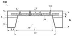
도 1a 및 1b는 본 개시의 실시예들에 따른 MEMS 디바이스들(10A 및 10B)의 개략적인 단면도를 도시한다.1A and 1B show schematic cross-sectional views of
일부 실시예에서, MEMS 디바이스들(10A 및 10B)은, 전자 회로(25)(예컨대, 상보적 금속-산화물-반도체(complementary metal-oxide-semiconductor; CMOS) 디바이스들과 같은 반도체 전계 효과 트랜지스터들을 포함하는 트랜지스터들)가 형성되는 회로 기판(20), 및 음향, 압력 및/또는 광을 수신하기 위한 개구(공동(cavity) 또는 리세스)(35)를 갖는 지지 기판(30)을 포함한다. 일부 실시예에서, 본딩 층(40)은 회로 기판(20)과 지지 기판(30) 사이에 형성된다. 일부 실시예에서, 본딩 층(40)은 실리콘 산화물 층이다. 일부 실시예에서, 회로 기판(20)은 전자 회로부에 의해 형성된 신호 프로세싱 회로 및/또는 증폭기 회로와 같은 전자 회로부(25)를 포함한다. 일부 실시예에서, 리세스(35)는 평면도에서 직사각형(예를 들어, 정사각형) 형상을 갖는다. 일부 실시예에서, 회로 기판(20) 및 지지 기판(30) 중 적어도 하나는 결정질 실리콘으로 제조된다. 일부 실시예에서, 도 1a에 도시된 바와 같이, 본딩 층은 리세스(35)의 하단에 남아 있고, 다른 실시예에서, 도 1b에 도시된 바와 같이, 본딩 층은 리세스(35)의 하단에 존재하지 않는다.In some embodiments,
또한, 일부 실시예에서, 도 1a 및 1b에 도시된 바와 같이, 회로 기판(20)의 전면 상에 제1 전도성 층(50)이 형성되고, 지지 기판(30)의 후면 상에 제2 전도성 층(55)이 형성된다. 일부 실시예에서, 도 1a에 도시된 바와 같이, 본딩 층(40)은 제2 전도성 층(55)과 접촉하고 회로 기판(20)과 접촉하지 않는다. 다른 실시예에서, 제2 전도성 층(55)은 도 1b에 도시된 바와 같이 회로 기판(20)과 접촉한다. 일부 실시예에서, 제1 및 제2 전도성 층은 Au, Ti, Cu, Ag 및 Ni의 하나 이상의 층을 포함한다.Further, in some embodiments, as shown in FIGS. 1A and 1B , a first
일부 실시예에서, 회로 기판(20)의 하단에 있는 리세스(35)의 크기의 거리(L1)는 약 10 mm 내지 약 50 mm 범위 내이고, 다른 실시예에서 약 15 mm 내지 약 20 mm 범위 내이다. 일부 실시예에서, 지지 기판(30)의 하단에 있는 공동(35)의 크기의 거리 L2는 L1보다 크고 약 11 mm 내지 약 52 mm 범위 내이며, 다른 실시예에서는 약 16 mm 내지 약 22 mm 범위 내이다. 일부 실시예에서, MEMS 디바이스의 에지 및 회로 기판(20)의 하단에 있는 리세스(35)의 에지로부터의 거리 L3(프레임 부분의 폭)는 약 2 ㎛ 내지 약 10 ㎛의 범위 내이고, 다른 실시예에서 약 3 ㎛ 내지 약 5 ㎛ 범위 내이다. 일부 실시예에서 본딩 층(40)의 두께 T1은 약 200 nm 내지 약 5 μm의 범위 내이며, 다른 실시예에서는 약 500 nm 내지 약 2 μm의 범위 내이다. 일부 실시예에서, MEM 디바이스의 총 두께 T2는 약 300 μm 내지 약 2 mm 범위 내이고, 다른 실시예에서는 약 600 μm 내지 약 800 μm 범위 내이다.In some embodiments, the distance L1 of the size of the
도 1c 및 1d는 본 개시의 실시예들에 따른 MEMS 디바이스들(10C 및 10D)의 개략적인 단면도를 도시한다. 일부 실시예에서, MEMS 디바이스(10C 및 10D)는, 하나 이상의 전자 또는 극 자외선(extreme ultraviolet; EUV) 광선이 MEMS 디바이스에 매립된 전자 회로의 동작에 의해 편향되는 빔 편향기이다.1C and 1D show schematic cross-sectional views of
MEMS 디바이스(10A 및 10B)와 유사하게, MEMS 디바이스(10C 및 10D)는, 전자 회로(25)가 형성되는 회로 기판(20)과, 음향, 압력 및/또는 광을 수신하기 위한 개구(공동 또는 리세스)(35)를 갖는 지지 기판(30)을 포함한다. 일부 실시예에서, 본딩 층(40)은 회로 기판(20)과 지지 기판(30) 사이에 형성된다. 일부 실시예에서, 본딩 층(40)은 실리콘 산화물 층이다. 일부 실시예에서, 하나 이상의 관통 홀(through holes)(60)이 회로 기판(20) 및 본딩 층(40)을 통과하게 배치되어 빔이 관통 홀(60)을 통과한다. 일부 실시예에서, 관통 홀(60)은 평면도에서 nxm 매트릭스로 배열되고, 여기서 n 및 m은 2 이상의 그리고 예를 들어, 128 이하의 정수이다.Similar to
일부 실시예에서, 도 1c 및 1d에 도시된 바와 같이, 회로 기판(20)의 전면 상에 제1 전도성 층(50)이 형성되고, 지지 기판(35)의 후면 상에 제2 전도성 층(55)이 형성된다. 일부 실시예에서, 도 1c에 도시된 바와 같이, 본딩 층(40)은 제2 전도성 층(55)과 접촉하고 회로 기판(20)과 접촉하지 않는다. 다른 실시예에서, 제2 전도성 층(55)은 도 1d에 도시된 바와 같이 회로 기판(20)과 접촉한다. 또한, 제1 전도성 층(50)과 제2 전도성 층(55)을 연결하는 관통 홀(60) 각각의 내벽 상에는 제3 전도성 층(57)이 배치된다.In some embodiments, as shown in FIGS. 1C and 1D , a first
일부 실시예에서, 회로 기판(20)은 전자 회로부에 의해 형성된 신호 프로세싱 회로 및/또는 증폭기 회로와 같은 전자 회로부(25)를 포함한다. 일부 실시예에서, 전자 회로부는 각각의 관통 홀(60)에서 제3 전도성 층의 전위를 제어하기 위해 제1, 제2 및/또는 제3 전도성 층에 결합되어, 관통 홀(60)을 통과하는 빔을 편향시킨다.In some embodiments,
일부 실시예에서, 리세스(35)는 평면도에서 직사각형(예를 들어, 정사각형) 형상을 갖는다. 일부 실시예에서, 회로 기판(20) 및 지지 기판(30) 중 적어도 하나는 결정질 실리콘으로 제조된다. 일부 실시예에서, 도 1c에 도시된 바와 같이, 본딩 층은 리세스(35)의 하단에 남아 있고, 다른 실시예에서, 도 1d에 도시된 바와 같이, 본딩 층은 리세스(35)의 하단에 존재하지 않는다. In some embodiments,
MEMS 디바이스(10C 및 10D)의 L1, L2 및 L3의 치수는 MEMS 디바이스(10A 및 10B)의 치수와 동일하거나 유사하다.The dimensions of L1, L2 and L3 of
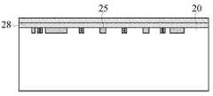
도 2a, 2b, 2c, 2d, 2e 및 2f는 본 개시의 실시예에 따른 MEMS 디바이스에 대한 제조 동작의 다양한 단계의 개략적인 단면도를 도시한다. 도 2a 내지 2f에 도시된 프로세스 이전, 도중 및 이후에 추가의 동작이 제공될 수 있으며, 아래 설명되는 동작 중 일부는 방법의 추가적인 실시예를 위해 대체 또는 제거될 수 있는 것으로 이해된다. 동작/프로세스의 순서가 상호 교환될 수 있다. 도 1 a 내지 1d와 관련하여 설명된 물질, 구성, 치수, 및 프로세스는 다음 실시예에 적용될 수 있고, 그 상세한 설명은 생략될 수 있다.2a, 2b, 2c, 2d, 2e and 2f show schematic cross-sectional views of various stages of a fabrication operation for a MEMS device in accordance with an embodiment of the present disclosure. It is understood that additional operations may be provided before, during, and after the process shown in FIGS. 2A-2F, and that some of the operations described below may be replaced or eliminated for additional embodiments of the method. The order of actions/processes may be interchanged. Materials, configurations, dimensions, and processes described in relation to FIGS. 1A to 1D may be applied to the following embodiments, and detailed descriptions thereof may be omitted.
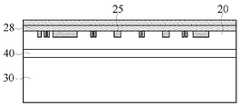
도 2a에 도시된 바와 같이, CMOS(complementary meta-oxide-semiconductor) 회로(25)는 회로 기판(20)의 전면 영역에 형성된다. 하나 이상의 패시베이션 막(28)이 회로 기판의 전면 위에 형성된다. 일부 실시예에서, 하나 이상의 패시베이션 막(28)은 실리콘 산화물, 실리콘 질화물, 또는 유기 막을 포함한다. 그 후, 도 2b에 도시된 바와 같이, 회로 기판(20)의 후면은 연삭 프로세스 또는 연마 프로세스에 의해 씨닝된다. 일부 실시예들에 있어, 씨닝된 회로 기판(20)의 잔여 두께는 약 100 μm 내지 약 500 μm 범위 내이다. As shown in FIG. 2A , a complementary meta-oxide-semiconductor (CMOS)
다음으로, 도 2c 및 2d에 도시된 바와 같이, 씨닝된 회로 기판(20)은 본딩 층(40)을 통해 지지 기판(30)에 본딩된다. 일부 실시예에서, 도 2c에 도시된 바와 같이, 본딩 층(40)은 예를 들어, 열 산화 프로세스 또는 화학적 증기 퇴적(chemical vapor deposition; CVD) 프로세스에 의해 지지 기판(30)의 표면 상에 형성된 실리콘 산화물이다. 다른 실시예에서, 본딩 층(40)은 예를 들어, CVD 프로세스에 의해 회로 기판(20)의 후면 상에 형성된다.Next, as shown in FIGS. 2C and 2D , the thinned
그 다음, 지지 기판(30)의 후면은 하나 이상의 리소그래피 및 에칭 동작을 사용하여 리세싱된다. 일부 실시예에서, 에칭 동작은 플라즈마 건식 에칭 또는 습식 에칭을 포함한다. 일부 실시예에서, 습식 에칭은 TMAH(tetramethylammonium hydroxide) 또는 KOH 용액을 사용한다.The back side of the supporting
일부 실시예에서, 본딩 층(40)은 도 2e에 도시된 바와 같이 리세스(35)를 형성하기 위한 에칭 정지 층으로서 기능한다. 일부 실시예에서, 하나 이상의 전도성 층이 지지 기판(30)의 후면 상에 그리고 본딩 층(40) 상에 형성된다.In some embodiments,
다른 실시예에서, 리세스 에칭이 본딩 층(40)에서 중지된 후, 본딩 층(40)은 하나 이상의 건식 에칭 동작 또는 습식 에칭 동작에 의해 추가로 에칭된다. 일부 실시예에서, 하나 이상의 전도성 층이 지지 기판(30)의 후면 상에 형성된다. 다른 실시예에서, 도 2f에 도시된 바와 같이, 본딩 층(40)이 제거된 후, 회로 기판(20)의 후면의 일부가 에칭된 다음 하나 이상의 전도성 층이 형성된다.In another embodiment, after the recess etch stops at
도 3a 내지 7b는 본 개시의 실시예에 따른 MEMS 디바이스에 대한 제조 동작의 다양한 단계의 개략적인 단면도를 도시한다. 도 3a 내지 7b에 도시된 프로세스 이전, 도중 및 이후에 추가의 동작이 제공될 수 있으며, 아래 설명되는 동작 중 일부는 방법의 추가적인 실시예를 위해 대체 또는 제거된다. 동작/프로세스의 순서는 상호 교환될 수 있다. 도 1 a 내지 1d 및 2a 내지 2f와 관련하여 설명된 물질, 구성, 치수, 및 프로세스는 다음 실시예에 적용될 수 있고, 그 상세한 설명은 생략될 수 있다. 3A-7B show schematic cross-sectional views of various stages of a fabrication operation for a MEMS device in accordance with an embodiment of the present disclosure. Additional operations may be provided before, during, and after the process shown in FIGS. 3A-7B , and some of the operations described below are replaced or eliminated for additional embodiments of the method. The order of actions/processes can be interchanged. Materials, configurations, dimensions, and processes described in relation to FIGS. 1A to 1D and 2A to 2F may be applied to the following embodiments, and detailed descriptions thereof may be omitted.
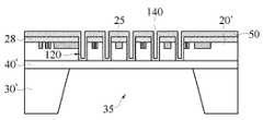
도 3a에 도시된 바와 같이, 회로 기판(20) 위에 전자 회로가 형성된 후, 하나 이상의 평면 전극(100)이 형성되고 하나 이상의 패시베이션 층(110)이 형성된다. 전극(100)은 회로 기판(20)에 형성된 전자 회로와 전기적으로 접속된다. 일부 실시예에서, 회로 기판(20)은 결정질 실리콘 기판을 포함한다. 일부 실시예에서, 하나 이상의 패시베이션 층에서 전극(100) 위에 하나 이상의 개구가 형성된다. 일부 실시예에서, 전극(100)은 Cu, Al, Au, Ni, Ag 또는 다른 적절한 전도성 물질의 하나 이상의 층으로 제조된다. 패시베이션 층(110)은 실리콘 질화물, SiON, 실리콘 산화물, 알루미늄 질화물 또는 유기 물질을 포함한다.As shown in FIG. 3A, after an electronic circuit is formed on the
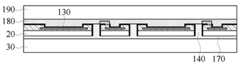
이어서, 관통 실리콘 비아(through-silicon-via; TSV)를 위한 하나 이상의 홀(120)이 전극(100) 이외의 영역에 형성된다. TSV 홀(120)은 하나 이상의 리소그래피 및 에칭 동작에 의해 형성된다. 일부 실시예에서, TSV 홀(120)은 평면도(도 7a 참조)에서 nxm 매트릭스로 배열되며, 여기서 n 및 m은 2 이상의 그리고 예를 들면, 128 이하의 정수이다. TSV의 깊이는 일부 실시예에서 패시베이션 층(110)의 상단으로부터 약 20 ㎛ 내지 약 100 ㎛의 범위 내에 있다. 일부 실시예에서, 깊이는 회로 기판의 후면의 씨닝 프로세스가 후속적으로 수행된 후에 TSV 홀(120)의 하단이 노출되도록 결정된다. 일부 실시예에서, 평면도에서 TSV 홀(120)의 형상은 원형 또는 직사각형(예를 들어, 정사각형)이다. 일부 실시예에서, TSV 홀(120)은 하단보다 더 큰 개구를 갖게 테이퍼링된다. 일부 실시예에서, 개구에서 TSV 홀(120)의 직경(또는 측부의 길이)은 약 100 nm 내지 약 12,000 nm 범위 내에 있다.Subsequently, one or
그 다음, 전극(100), 패시베이션 층(110) 위에 그리고 TSV 홀(120) 내부에 제1 전도성 층(130)이 형성된다. 그 다음, 도 3b에 도시된 바와 같이 TSV 홀(120)을 채우도록 충전 층(140)이 형성된다. 제1 전도성 층(130)은 도 1a 내지 1d에 도시된 제1 전도성 층(50)과 동일하거나 유사한 기능을 갖는다. 일부 실시예에서, 제1 전도성 층(130)은 Au, Ti, Cu, Ag 및 Ni의 하나 이상의 층을 포함한다. 특정 실시예에서, Ti 층 위에 형성된 금 층이 제1 전도성 층(130)으로서 사용된다. 일부 실시예에서 Ti 층의 두께는 약 50 nm 내지 약 500 μm의 범위 내이며, 다른 실시예에서 약 80 nm 내지 약 300 nm의 범위 내이다. 일부 실시예에서 금(Au)의 두께는 약 10 nm 내지 약 10,000 nm의 범위 내이며, 다른 실시예에서 약 150 nm 내지 약 250 nm의 범위 내이다. 일부 실시예에서, 충전 층(140)은 실리콘 산화물 또는 임의의 다른 적절한 절연 물질을 포함한다. 일부 실시예에서, 충전 물질의 블랭킷 층은 제1 전도성층(130) 위에 형성되고, 그 다음에 화학 기계적 연마 프로세스 또는 에칭백 프로세스와 같은 평탄화 동작이 수행되어, 도 3b에 도시된 바와 같이, 충전 물질을 TSV 홀(120) 내에만 남겨둔다. 다른 실시예에서, 충전 물질은 또한 전극(100) 위의 오목한 부분 상에 남아있다.A first
다음으로, 도 3c에 도시된 바와 같이, 전도성 층(130)은 TSV 홀(120) 근처의 패시베이션 층(110) 위에 하나 이상의 개구를 형성하도록 패터닝되어 패시베이션 층을 부분적으로 노출시킨다. 이어서, 절연 층이 형성되고 패터닝되어 개구를 덮는 섬형(island shaped) 절연 패턴(150)을 형성한다. 일부 실시예에서, 절연 패턴(150)은 실리콘 질화물을 포함한다. Next, as shown in FIG. 3C ,
또한, 도 3d에 도시된 바와 같이, 위에 전도성 층(130) 및 패턴(150)이 형성되는 회로 기판(20)의 전면 위에 제1 캐리어 본딩 층(160)이 형성된 후 제1 캐리어 기판(165)이 부착된다. 제1 캐리어 기판(165)은 일부 실시예에서 유리 기판, 세라믹 기판, 반도체 기판 또는 수지 기판이다. 일부 실시예에서, 제1 캐리어 본딩 층(160)은 유기 물질, 실리콘 산화물 또는 임의의 다른 적절한 물질을 포함한다.In addition, as shown in FIG. 3D, after the first
그 후, 회로 기판(20)의 후면은 연삭 또는 연마(예를 들어, CMP) 동작에 의해 씨닝된다. 일부 실시예에서, 씨닝 후, 회로 기판(20)은 약 20 ㎛ 내지 약 300 ㎛ 범위 내의 잔여 두께를 가지며, 잔여 두께는 다른 실시예들에서 약 40 ㎛ 내지 약 180 ㎛ 범위 내이다. 도 3d에 도시된 바와 같이, TSV 홀(120)에 채워진 충전 물질 층(140)의 하단이 노출된다. 다른 실시예에서, 씨닝 동작 후에, 제1 캐리어 기판(165)은 회로 기판(20)의 전면에 부착된다.Then, the back side of the
또한, 도 3e에 도시된 바와 같이, 회로 기판(20)의 씨닝된 후면 상에 본딩 층(170)이 형성된다. 본딩 층(170)은 도 1a 내지 2f에 도시된 본딩 층(40)과 동일하거나 유사한 기능을 갖는다. 일부 실시예에서, 본딩 층(170)은 예를 들어, CVD 프로세스에 의해 형성된 실리콘 산화물을 포함한다.Also, as shown in FIG. 3E , a
이어서, 도 4a에 도시된 바와 같이, 지지 기판(30)이 준비되고 본딩 층(170)을 통해 회로 기판(20)에 본딩된다(산화물 융합 본딩). 일부 실시예에서, 지지 기판(30)은 결정질 실리콘으로 제조된다. 산화물 융합 본딩 후, 도 4b에 도시된 바와 같이, 제1 캐리어 기판(165) 및 제1 캐리어 본딩 층(160)이 제거된다. 도 4a에 도시된 바와 같이, 본딩층(170)은 TSV 홀(120) 내의 충전 물질 층(140)에 접속된다. 일부 실시예에서, 본딩 층(170)과 충전 물질 층(140)은 동일 물질로 제조된다.Then, as shown in FIG. 4A, the
다른 실시예에서, 본딩 층(170)은 지지 기판(30) 상에, 또는 지지 기판(30)과 회로 기판(20) 모두 상에 형성된다. 일부 실시예에서, 본딩 층이 없는 지지 기판(30)의 두께는 약 200 μm 내지 약 1.8 mm 범위 내이고, 다른 실시예에서 약 500 μm 내지 약 750 μm 범위 내이다.In another embodiment,
다음으로, 도 4c에 도시된 바와 같이, 제1 하드 마스크 층(180)이 형성된 후 회로 기판(20)의 전면 위에 제2 하드 마스크 층(190)이 형성된다. 일부 실시예에서, 제1 하드 마스크 층(180)은 실리콘 산화물을 포함하고, 제2 하드 마스크 층(190)은 폴리실리콘 또는 비정질 실리콘을 포함한다. 일부 실시예들에서, 실리콘 산화물 하드 마스크 층(180)은 CVD 프로세스에 의해 형성된 다음, CMP 동작과 같은 평탄화 프로세스가 수행된다. 유사하게, 일부 실시예에서, 폴리실리콘 하드 마스크 층(190)이 화학적 증기 퇴적(CVD)에 의해 형성된 다음 CMP 동작이 선택적으로 수행된다. 일부 실시예에서, 폴리실리콘 하드 마스크 층(190)의 두께는 약 30 μm 내지 약 70 μm의 범위 내이다.Next, as shown in FIG. 4C , after the first
그 다음, 하나 이상의 리소그래피 및 에칭 동작을 사용함으로써, 제2 하드 마스크 층(190) 및 제1 하드 마스크 층(180)은 도 4d에 도시된 바와 같이 전극(100) 위에 하나 이상의 개구(200)를 형성하도록 패터닝된다. 일부 실시예에서, 개구(200)의 크기는 전극(100) 위의 패시베이션 층(110)에 형성된 개구의 크기보다 크다. 또한, 일부 실시예에서 절연 패턴(150)은 도 4d에 도시된 바와 같이 개구(200)에서 부분적으로 노출된다.Then, by using one or more lithography and etching operations, the second
다음으로, 도 5a에 도시된 바와 같이, 하나 이상의 전도성 층(210)(필라 전극(pillar electrode))이 개구(200)에 형성된다. 일부 실시예에서, 전도성 층은 도금 동작(전기 도금 또는 무전해 도금)에 의해 형성된 금 또는 금 합금(예를 들어, AuCu 및 AuNi)을 포함한다. 일부 실시예에서, 도금된 전도성 층(210)의 두께는 약 20 μm 내지 약 50 μm의 범위 내이다. 일부 실시예에서, 도금된 전도성 층(210)의 두께(높이)는 도 5a에 도시된 바와 같이 제2 하드 마스크 층(190)의 상단보다 작다.Next, as shown in FIG. 5A , one or more conductive layers 210 (pillar electrodes) are formed in the
또한, 도 5b에 도시된 바와 같이, 하나 이상의 전극(100) 위의 도금층(210)의 일부는 마스크 패턴(220)에 의해 덮인다. 일부 실시예에서, 마스크 패턴(220)은 포토 레지스트 패턴을 포함한다. 그 후, 추가 전도성 층(215)(필라 전극)이 전도성 도금층(210) 위에 형성된다. 일부 실시예에서, 추가 전도성 층(215)은 도금 동작(전기 도금 또는 무전해 도금)에 의해 형성된다. 일부 실시예에서, 추가 전도성 층(215)은 도금된 전도성 층(210)과 동일한 물질로 제조되고, 금 또는 금 합금(예를 들어, AuCu, AuNi)을 포함한다. 다른 실시예에서, 추가 전도성 층(215)은 도금된 전도성 층(210)과는 다른 물질로 제조된다. 그 후, 도 5c에 도시된 바와 같이 포토 레지스트 패턴(220)이 제거된다.Also, as shown in FIG. 5B , a portion of the
일부 실시예에서, 추가 전도성 층(215)의 두께는 약 10 μm 내지 약 35 μm의 범위 내이다. 일부 실시예에서, 도금된 전도성 층(210) 및 추가 전도성 층(220)의 총 두께(높이)는 도 5c에 도시된 바와 같이 제2 하드 마스크 층(190)의 상단보다 작다. 일부 실시예에서, 도금된 전도성 층(210/220)의 2개의 상이한 두께(높이)는 상이한 전기 회로부를 제어한다. 예를 들어, 더 높은 것은 전자를 보호하는(shelter) 데 사용되고 더 낮은 것은 전기장을 제어하는 데 사용된다.In some embodiments, the thickness of the additional
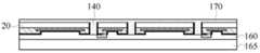
이어서, 도 6a에 도시된 바와 같이, 회로 기판(20)의 전면 위에 제2 캐리어 본딩 층(305)이 형성되고, 제2 캐리어 본딩 층(305)을 통해 회로 기판(20)의 전면에 제2 캐리어 기판(300)이 부착된다. 제2 캐리어 기판(300)은 일부 실시예에서 유리 기판, 세라믹 기판, 반도체 기판 또는 수지 기판이다. 일부 실시예에서, 제2 캐리어 본딩 층(305)은 유기 물질, 실리콘 산화물 또는 임의의 다른 적절한 물질을 포함한다.Subsequently, as shown in FIG. 6A, a second
그 다음, 전체 기판이 수직으로 뒤집힌(flipped) 다음 지지 기판(30)의 후면이 패터닝되어 리세스(35)를 형성한다. 일부 실시예에서, 리세스(35)는 마스크 패턴(310)을 사용하여 하나 이상의 리소그래피 및 에칭 동작에 의해 형성된다. 일부 실시예에서, 마스크 패턴(35)은 포토 레지스트로 제조된다.The entire substrate is then vertically flipped and then the back side of the supporting
일부 실시예에서, 에칭 동작은 플라즈마 건식 에칭 또는 습식 에칭을 포함한다. 일부 실시예에서, 본딩 층(170)은 리세스(35)를 형성하기 위한 에칭 정지 층으로서 기능한다. 리세스(35)를 형성하기 위해 플라즈마 건식 에칭 프로세스가 사용되는 경우, 플라즈마 에칭은 실질적으로 본딩 층(170)에서 중지되어 회로 기판(20)에 형성된 전자 회로 상의 플라즈마 손상이 방지될 수 있다.In some embodiments, the etching operation includes a plasma dry etch or wet etch. In some embodiments,
일부 실시예에서, 리세스 에칭이 본딩 층(170)에서 중지된 후, 본딩 층(170)은 하나 이상의 건식 에칭 또는 습식 에칭 동작에 의해 추가로 에칭된다. 일부 실시예에서, 본딩 층의 에칭은 회로 기판(20)(예를 들어, Si)에 대해 높은 선택성을 갖는다. 예를 들어, 본딩 층의 에칭 속도는 회로 기판(20)의 에칭 속도의 10배 이상이다. 일부 실시예에서, 본딩 층(170)이 실리콘 산화물로 제조되는 경우, 회로 기판(20)에 형성된 전자 회로의 손상을 억제하기 위해 HF 또는 버퍼링된 HF를 사용하는 습식 에칭 프로세스가 수행된다. 본딩 층(170)을 제거할 때, 충전 물질 층(140)이 본딩 층(170)과 동일한 물질(예를 들어, 실리콘 산화물)로 제조되면 TSV 홀(120) 내의 충전 물질 층(140)도 제거된다. 충전 물질 층(140)이 본딩 층(170)과 다른 물질(예를 들어, 실리콘 질화물)로 제조되는 경우, 충전 물질 층(140)을 제거하기 위해 습식 에칭 동작과 같은 추가 에칭 동작이 수행된다.In some embodiments, after the recess etch stops at
충전 물질 층(140)이 TSV 홀(120)에서 제거된 후, 도 6b에 도시된 바와 같이 리세스(35) 내부에 제2 전도성 층(320)이 형성된다.After the filling
일부 실시예에서, 도 6b에 도시된 바와 같이, 제2 전도성 층(320)은 각 TSV 홀(120)의 내벽 상에 형성된 제1 전도성 층(130)과 접촉하도록 형성된다. 일부 실시예에서, 제2 전도성 층(320)은 또한 제1 전도성 층(130)이 이미 형성된 TSV 홀(120)의 내벽 상에 형성된다. 일부 실시예에서, 제2 전도성 층(320)은 제1 전도성 층(130)과 동일하거나 상이한 물질로 제조되고 Au, Ti, Cu, Ag 및 Ni의 하나 이상의 층을 포함한다. 특정 실시예에서, Ti 층 위에 형성된 금 층이 제2 전도성 층(320)으로 사용된다. 일부 실시예에서 Ti 층의 두께는 약 50 nm 내지 약 200 mm의 범위 내이며, 다른 실시예에서는 약 80 nm 내지 약 120 nm의 범위 내이다. 일부 실시예에서 금(Au) 층의 두께는 약 10 nm 내지 약 400 nm의 범위 내이며, 다른 실시예에서는 약 150 nm 내지 약 250 nm의 범위 내이다.In some embodiments, as shown in FIG. 6B , the second
일부 실시예에서, 복수의 MEMS 디바이스가 Si 웨이퍼 상에 형성되고 웨이퍼는 스크라이브 라인(390)에서 쏘잉(다이싱 동작)에 의해 개별 MEMS 디바이스(칩)로 절단된다. 일부 실시예에서, 다이싱 동작은 도 6b에 도시된 바와 같이 지지 제2 캐리어 본딩 층(305)을 완전히 절단하지 않는다. 제2 캐리어 본딩 층(305)을 제거하고 이에 따라 제2 캐리어 기판(300)을 제거함으로써, 개별 MEMS 디바이스가 릴리스된다.In some embodiments, a plurality of MEMS devices are formed on a Si wafer and the wafer is cut into individual MEMS devices (chips) by sawing (dicing operation) at a
일부 실시예에서, 다이싱 동작은 제2 전도성 층(320)이 형성된 후에 수행된다. 이 경우 MEMS 디바이스의 측부면(다이싱된 면) 상에는 전도성 층이 형성되지 않는다. 다른 실시예에서, 다이싱 동작은 제2 전도성 층(320)이 형성되기 전에 수행된다. 이 경우, 제2 전도성 층(320)도 MEMS 디바이스의 측부면에 형성된다.In some embodiments, the dicing operation is performed after second
일부 실시예에서, 제2 캐리어 기판(300) 및 제2 캐리어 본딩 층(305)이 제거된 후, 개별 MEMS 디바이스는 도 6c에 도시된 바와 같이 프레임(400) 상에 부착된다. 도 6c에 도시된 바와 같이, 제2 캐리어 기판(300) 및 제2 캐리어 본딩 층(305)을 제거함으로써 TSV 홀(120)이 노출되어 전자빔 또는 광선이 통과할 수 있다.In some embodiments, after the
도 7a는 MEMS 디바이스의 평면도를 도시하고, 도 7b는 주변 영역(peripheral region; PR)에서 본딩 패드 구조물의 단면도를 도시한다. 도 7a의 평면도에 도시된 바와 같이, MEMS 디바이스는 중심 영역(center region; CR) 및 중심 영역을 둘러싸는 주변 영역을 갖는다. TSV 홀(120) 및 전도성 층(210/220)은 중앙 영역(CR)에 배치된다. 주변 영역(PR)에는, 하나 이상의 언더 범프 패드 전극(250)이 형성되어 회로 기판(20)에 형성된 전자 회로를 MEMS 디바이스 외부의 하나 이상의 회로에 접속한다. 일부 실시예에서, 주변 영역(PR)은 평면도에서 리세스(35)와 중첩하지 않는다. 다른 실시예에서, 주변 영역(PR)은 평면도에서 리세스(35)와 부분적으로 중첩한다.Figure 7a shows a top view of the MEMS device, and Figure 7b shows a cross-sectional view of the bonding pad structure in the peripheral region (PR). As shown in the plan view of FIG. 7A, the MEMS device has a center region (CR) and a peripheral region surrounding the center region. The
언더 범프 패드 전극(250)은 회로 기판(20)의 전면 상에 형성된다. 일부 실시예에서, 언더 범프 패드 전극(250)은 주변 영역(PR)에서 매트릭스로 배열된다. 일부 실시예에서, 볼 범프(260)는 언더 범프 패드 전극(250) 각각 상에 배치된다. 일부 실시예에서, 언더 범프 패드 전극(250)은 도 6a에 도시된 바와 같이 리세스 에칭 전에 형성된다. 일부 실시예에서, 언더 범프 패드 전극(250)은, 지지 기판(30)이 도 4a 및 4b에 도시된 바와 같이 산화물 융합 본딩을 통해 회로 기판(20)에 부착된 후에 형성된다. The under
일부 실시예에서 언더 범프 패드 전극(250)은, 층간 유전체 층(230)에 매립되고 전자 회로의 최상부 금속 층(예를 들어, 8번째 내지 12번째 금속 레벨)으로 형성되는 금속 패드(225) 상에 형성된다. 일부 실시예에서, 금속 패드(225)는 전도성 물질의 하나 이상의 층을 포함한다. 일부 실시예에서, 금속 패드(225)는 Cu 또는 Cu 합금을 포함한다. In some embodiments, the under
또한, 도 7b에 도시된 바와 같이, 언더 범프 패드 전극(250)은 전도성 물질의 다중 층을 포함한다. 일부 실시예에서, 언더 범프 패드 전극(250)은 제1 금속성 층(252), 제2 금속성 층(254), 제3 금속성 층(256), 및 제4 금속성 층(258)을 포함한다. 일부 실시예에서, 제1 금속성 층은 TiW 층이고, 제2 금속성 층은 Cu 층이고, 제3 금속성 층은 Ni 층이며, 제4 금속성 층은 Sn 층이다.Also, as shown in FIG. 7B , the under
일부 실시예에서 TiW 층(252)의 두께는 약 50 nm 내지 약 1000 μm의 범위 내이며, 다른 실시예에서는 약 100 nm 내지 약 500 nm의 범위 내이다. 일부 실시예에서 Cu 층(254)의 두께는 약 10 nm 내지 약 2000 μm의 범위 내이며, 다른 실시예에서는 약 500 nm 내지 약 1000 nm의 범위 내이다. 일부 실시예에서 Ni 층(256)의 두께는 약 1000 nm 내지 약 5000 μm의 범위 내이며, 다른 실시예에서는 약 2500 nm 내지 약 3500 nm의 범위 내이다. 일부 실시예에서 Sn 층(258)의 두께는 약 500 nm 내지 약 4000 nm의 범위 내이며, 다른 실시예에서는 약 1500 nm 내지 약 2500 nm의 범위 내이다. 금속성 층은 CVD, 스퍼터링을 포함하는 물리적 증기 퇴적(physical vapor deposition; PVD), 도금 또는 임의의 다른 적절한 막 형성 방법, 그리고 리소그래피 및 에칭 동작 중 하나 이상에 의해 형성된다.The thickness of
일부 실시예에서, 전자 회로의 표면은 하나 이상의 패시베이션 층으로 덮인다. 일부 실시예에서, 패시베이션 층은 제1 패시베이션 층(242), 제2 패시베이션 층(244) 및 제3 패시베이션 층(246)을 포함한다. 언더 범프 패드 전극(250)은 도 7b에 도시된 바와 같이 패시베이션 층에 형성된 개구에 형성된다. 일부 실시예에서, 제1 패시베이션 층(242)은 SiC 층이고, 제2 패시베이션 층(244)은 실리콘 산화물 층이며, 제3 패시베이션 층(246)은 실리콘 질화물 층이다.In some embodiments, the surface of the electronic circuitry is covered with one or more passivation layers. In some embodiments, the passivation layer includes a
도 8은 본 개시의 실시예에 따른 MEM 디바이스의 사용을 도시한다. 일부 실시예에서, MEMS 디바이스(10)는 전자 또는 전자기파 리소그래피에 사용된다. 일부 실시예에서, 전자 빔(또는 EUV 광선)(500)은 회로 기판(20)의 전면으로부터 MEMS 디바이스(10)로 입력된다. 회로 기판(20)에 형성된 전자 회로는 각 TSV 홀(120)의 내벽 상에 형성된 전도성 층(예를 들어, 제1 전도성 층(130))에 인가되는 전압을 독립적으로 제어한다. TSV 홀(120)의 전도성 층에 인가되는 전압을 조절함으로써, 전자빔(500)의 일부는 하나 이상의 TSV 홀을 통과하고 전자빔(500)의 일부는 TSV 홀을 통과하지 않는다. TSV 홀을 통과하는 전자빔의 일부는 그 위에 포토 레지스트 층이 형성되는 웨이퍼 또는 기판에 지향된다. 일부 실시예에서, 웨이퍼는 반도체 웨이퍼이다. 일부 실시예에서, 기판은 투명 기판 또는 반사 기판과 같이 포토 마스크를 위한 것이다. 전자 회로를 제어함으로써 전자빔을 통과하는 TSV 홀(120)의 위치가 제어되어 포토 레지스트 패턴 상에 원하는 형상이 그려질 수 있다.8 illustrates the use of a MEM device according to an embodiment of the present disclosure. In some embodiments, MEMS device 10 is used for electronic or electromagnetic wave lithography. In some embodiments, electron beam (or EUV light) 500 is input into MEMS device 10 from the front side of
다른 실시예에서, SOI(silicon-on-insulator) 웨이퍼가 사용된다. 이 경우, 융합 본딩 프로세스가 생략되고, SOI 웨이퍼의 산화물 층이 리세스 에칭에서 에칭 정지 층으로서 기능한다. 도 9a, 9b, 9c, 및 9d는 본 개시의 실시예에 따른 MEMS 디바이스에 대한 제조 동작의 다양한 단계의 개략적인 단면도를 도시한다. 도 9a 내지 9d에 도시된 프로세스 이전, 도중 및 이후에 추가적인 동작이 제공될 수 있으며, 아래 설명되는 동작 중 일부는 방법의 추가적인 실시예를 위해 대체 또는 제거될 수 있는 것으로 이해된다. 동작/프로세스의 순서가 상호 교환될 수 있다. 도 1a 내지 7b와 관련하여 설명된 물질, 구성, 치수, 및 프로세스는 다음 실시예에 적용될 수 있고, 그 상세한 설명은 생략될 수 있다.In another embodiment, a silicon-on-insulator (SOI) wafer is used. In this case, the fusion bonding process is omitted, and the oxide layer of the SOI wafer functions as an etch stop layer in the recess etch. 9A, 9B, 9C, and 9D show schematic cross-sectional views of various stages of a fabrication operation for a MEMS device in accordance with an embodiment of the present disclosure. It is understood that additional operations may be provided before, during, and after the processes depicted in FIGS. 9A-9D , and that some of the operations described below may be replaced or eliminated for additional embodiments of the method. The order of actions/processes may be interchanged. Materials, configurations, dimensions, and processes described in relation to FIGS. 1A to 7B may be applied to the following embodiments, and detailed descriptions thereof may be omitted.
SOI 기판은 도 9a에 도시된 바와 같이 디바이스 층(반도체 층)(20'), 산화물 층(40') 및 벌크 층(반도체 기판)(30')을 포함한다.The SOI substrate includes a device layer (semiconductor layer) 20', an oxide layer 40' and a bulk layer (semiconductor substrate) 30' as shown in Fig. 9A.
도 9a에 도시된 바와 같이, CMOS 회로(25)는 디바이스 층(20')의 전면 영역에 형성된다. 하나 이상의 패시베이션 막(28)이 디바이스 층(20')의 전면 위에 형성된다. 일부 실시예에서, 하나 이상의 패시베이션 막(28)은 실리콘 산화물, 실리콘 질화물, 또는 유기 막을 포함한다. 일부 실시예에서, 충전 물질(140)로 채워진 TSV 홀(120)은 디바이스 층(20')을 통과하여 형성된다. 또한, 하나 이상의 제1 전도성 층(50)이 도 9a에 도시된 바와 같이 디바이스 층의 전면 상에 그리고 TSV 홀 내에 형성된다.As shown in Fig. 9A, a
그러면, 도 9b에 도시된 바와 같이, 벌크 층(30')의 후면은 하나 이상의 리소그래피 및 에칭 동작을 사용하여 리세싱된다. 일부 실시예에서, 에칭 동작은 플라즈마 건식 에칭 또는 습식 에칭을 포함한다. 일부 실시예에서, 습식 에칭은 TMAH(tetramethylammonium hydroxide) 또는 KOH 용액을 사용한다.Then, as shown in FIG. 9B, the back side of bulk layer 30' is recessed using one or more lithography and etching operations. In some embodiments, the etching operation includes a plasma dry etch or wet etch. In some embodiments, wet etching uses a tetramethylammonium hydroxide (TMAH) or KOH solution.
일부 실시예에서, 산화물 층(40')은 도 9b에 도시된 바와 같이 리세스(35)를 형성하기 위한 에칭 정지 층으로서 기능한다.In some embodiments, oxide layer 40' functions as an etch stop layer for forming
리세스 에칭이 산화물 층(40')에서 중지된 후, 산화물 층(40')은 하나 이상의 건식 에칭 또는 습식 에칭 동작에 의해 추가로 에칭된다. 산화물 층(40')을 에칭하는 동안, 도 9c에 도시된 바와 같이, 충전 물질 층(140)도 TSV 홀(120)에서 제거된다.After the recess etch stops on the oxide layer 40', the oxide layer 40' is further etched by one or more dry etch or wet etch operations. While etching the oxide layer 40', the
일부 실시예에서, 하나 이상의 제2 전도성 층(55)이 도 9d에 도시된 바와 같이 벌크 층(30')의 후면 상에 형성된다.In some embodiments, one or more second
본 개시의 실시예들에서, MEMS 디바이스는 산화물 융합 본딩에 의해 실리콘 산화물 본딩 층을 통해 회로 기판과 지지 기판을 본딩하거나 SOI 기판을 사용하여 형성된다. 산화물 본딩 층(산화물 층)은, 지지 기판이 에칭되어 리세스를 형성할 때 플라즈마 건식 에칭을 위한 에칭 정지 층으로 또한 기능하여, 플라즈마 에칭으로 인한 손상으로부터, 회로 기판에 형성된 전자 회로부를 보호한다. 실리콘 산화물 본딩 층은 습식 에칭 동작에 의해 제거될 수 있기 때문에, 실리콘 산화물 본딩 층의 제거 프로세스는 회로 기판에 형성된 전자 회로부에 손상을 일으키지 않는다.In embodiments of the present disclosure, a MEMS device is formed using an SOI substrate or bonding a circuit board and a support substrate through a silicon oxide bonding layer by oxide fusion bonding. The oxide bonding layer (oxide layer) also functions as an etching stop layer for plasma dry etching when the support substrate is etched to form a recess, thereby protecting electronic circuitry formed on the circuit board from damage due to plasma etching. Since the silicon oxide bonding layer can be removed by a wet etching operation, the process of removing the silicon oxide bonding layer does not cause damage to the electronic circuitry formed on the circuit board.
본 개시에서 설명된 다양한 실시예들 및 예시들은 위에서 명시된 대로, 기존 기술에 비해 여러 가지 이점을 제공한다. 모든 장점들이 기본적으로 여기에 논의된 것은 아니며 모든 실시예 또는 예시에 대해 특정 장점이 요구되는 것이 아니며, 다른 실시예 또는 예시가 상이한 장점들을 제공할 수 있는 것으로 이해될 것이다.The various embodiments and examples described in this disclosure provide several advantages over existing technologies, as noted above. It will be understood that not all advantages are discussed herein by default and that no particular advantage is required for every embodiment or example, and that other embodiments or examples may provide different advantages.
본 개시의 한 양상에 따라, 마이크로 전자 기계 시스템(MEMS)은, 전자 회로부를 포함하는 회로 기판; 리세스를 갖는 지지 기판; 회로 기판과 지지 기판 사이에 배치된 본딩 층; 회로 기판을 관통해 개구로 통과하는 관통 홀; 회로 기판의 전면 상에 배치된 제1 전도성 층; 리세스의 내벽 상에 배치된 제2 전도성 층; 및 관통 홀 각각의 내벽 상에 배치된 제3 전도성 층을 포함한다. 전술된 그리고 후술된 실시예들 중 하나 이상에서, 본딩 층은 실리콘 산화물을 포함한다. 전술된 그리고 후술된 실시예들 중 하나 이상에서, 리세스에는 본딩 층이 배치되지 않고, 회로 기판의 하단이 제2 전도성 층과 접촉한다. 전술된 그리고 후술된 실시예들 중 하나 이상에서, 회로 기판은 상이한 구성을 갖는 전극을 포함한다. 전술된 그리고 후술된 실시예들 중 하나 이상에서, 전극은 제1 전극 및 제2 전극을 포함하고, 제1 전극 각각 상에 제1 필라 전극이 배치되고, 제2 전극 각각 상에 제2 필라가 배치되며, 제1 필라 전극의 높이는 제2 필라 전극의 높이와 다르다. 전술된 그리고 후술된 실시예들 중 하나 이상에서, 제1 필라 전극과 제2 필라 전극의 높이 차이는 10 μm 내지 30 μm. 범위 내이다. 전술된 그리고 후술된 실시예들 중 하나 이상에서, 평면도에서, 회로 기판은 관통 홀이 제공되는 중심 영역과 중심 영역을 둘러싸는 주변 영역을 포함하고, 전극과는 다른 구성을 갖는 복수의 범프 전극이 주변 영역에 배치된다. 및 다음 실시예 중 하나 이상에서, 주변 영역은 평면도에서 리세스와 중첩되지 않는다.According to one aspect of the present disclosure, a microelectromechanical system (MEMS) includes a circuit board including electronic circuitry; a supporting substrate having a recess; a bonding layer disposed between the circuit board and the supporting substrate; a through hole passing through the circuit board to the opening; a first conductive layer disposed on the front surface of the circuit board; a second conductive layer disposed on an inner wall of the recess; and a third conductive layer disposed on an inner wall of each through hole. In one or more of the above and below described embodiments, the bonding layer includes silicon oxide. In one or more of the above and below described embodiments, no bonding layer is disposed in the recess, and the bottom of the circuit board is in contact with the second conductive layer. In one or more of the above and below described embodiments, the circuit board includes electrodes having different configurations. In one or more of the above and below described embodiments, the electrode includes a first electrode and a second electrode, a first pillar electrode is disposed on each of the first electrodes, and a second pillar is disposed on each of the second electrodes. The height of the first pillar electrode is different from that of the second pillar electrode. In one or more of the above-mentioned and below-mentioned embodiments, the height difference between the first pillar electrode and the second pillar electrode is 10 μm to 30 μm. is within range In one or more of the foregoing and later-described embodiments, in plan view, the circuit board includes a central region in which a through hole is provided and a peripheral region surrounding the central region, and a plurality of bump electrodes having a configuration different from the electrodes are provided. placed in the surrounding area. and in one or more of the following embodiments, the peripheral region does not overlap the recess in plan view.
본 개시의 또 다른 양상에 따라, 마이크로 전자 기계 시스템(MEMS)을 제조하는 방법에서, 전자 회로가 제1 기판의 전면 위에 형성되고, 제1 기판 내로 관통하는 하나 이상의 홀이 형성되고, 홀은 충전 물질로 채워지고, 제1 기판의 후면이 씨닝되어 채워진 홀의 일부를 노출시키고, 본딩 층이 제2 기판과 제1 기판의 후면 사이에 개재되면서 제2 기판이 제1 기판의 후면에 본딩되고, 리세스가 제2 기판에 형성되어 제1 기판의 하단이 노출된다. 전술된 그리고 후술된 실시예들 중 하나 이상에서, 본딩 층은 실리콘 산화물이다. 전술된 그리고 후술된 실시예들 중 하나 이상에서, 본딩 층은 제1 기판의 후면 상에 형성된다. 전술된 그리고 후술된 실시예들 중 하나 이상에서, 본딩 층은 제2 기판 상에 형성된다. 전술된 그리고 후술된 실시예들 중 하나 이상에서, 리세스가 형성될 때, 제2 기판의 일부는 본딩 층을 노출시키기 위해 플라즈마 건식 에칭에 의해 에칭되지만 제1 기판은 에칭되지 않고, 제1 기판으로부터 본딩 층을 선택적으로 제거하는 에칭에 의해 본딩 층이 에칭된다. 전술된 그리고 후술된 실시예들 중 하나 이상에서, 본딩 층을 에칭할 때, 충전 물질이 또한 홀로부터 제거되어 관통 홀을 형성한다. 전술된 그리고 후술된 실시예들 중 하나 이상에서, 제1 전도성 층이 제1 기판의 전면 위에 그리고 각 홀의 내벽 상에 형성되고, 제2 전도성 층이 리세스의 내벽 위에 형성된다. 전술된 그리고 후술된 실시예들 중 하나 이상에서, 제1 전도성 층 및 제2 전도성 층 중 적어도 하나는 Ti 층 상의 Au 층의 적층된 층이다. 전술된 그리고 후술된 실시예들 중 하나 이상에서, 홀은 평면도에서 매트릭스로 배열된다.According to another aspect of the present disclosure, in a method of manufacturing a microelectromechanical system (MEMS), an electronic circuit is formed over the front surface of a first substrate, one or more holes penetrating into the first substrate are formed, and the holes are filled. filled with a material, the back surface of the first substrate is thinned to expose a portion of the filled hole, and the second substrate is bonded to the back surface of the first substrate while a bonding layer is interposed between the second substrate and the back surface of the first substrate; A set is formed on the second substrate to expose a lower end of the first substrate. In one or more of the above and below described embodiments, the bonding layer is silicon oxide. In one or more of the above and below described embodiments, a bonding layer is formed on the back side of the first substrate. In one or more of the above and below described embodiments, a bonding layer is formed on the second substrate. In one or more of the above and below described embodiments, when the recess is formed, a portion of the second substrate is etched by plasma dry etching to expose the bonding layer but the first substrate is not etched, and the first substrate The bonding layer is etched by an etch that selectively removes the bonding layer from the substrate. In one or more of the above and below described embodiments, when etching the bonding layer, the filling material is also removed from the hole to form a through hole. In one or more of the above and below described embodiments, a first conductive layer is formed over the front surface of the first substrate and on an inner wall of each hole, and a second conductive layer is formed over an inner wall of the recess. In one or more of the embodiments described above and below, at least one of the first conductive layer and the second conductive layer is a stacked layer of an Au layer on a Ti layer. In one or more of the embodiments described above and below, the holes are arranged in a matrix in plan view.
본 개시의 또 다른 양상에 따라, 마이크로 전자 기계 시스템(MEMS)을 제조하는 방법에서, 전자 회로는 제1 기판의 전면 위에 형성되고, 전극은 제1 기판 위에 형성되고, 제1 기판 내로 관통하는 하나 이상의 홀은, 형성되고 있는 전극 이외의 영역에 형성되고, 홀은 충전 물질로 채워지고, 제1 기판의 후면이 씨닝되어 채워진 홀의 일부를 노출하고, 실리콘 산화물로 제조된 본딩 층이 제2 기판과 제1 기판의 후면 사이에 개재되면서 제2 기판이 제1 기판의 후면에 본딩되고, 필라 전극이 각각 전극 위에 형성되며, 리세스가 제2 기판에 형성되어, 제1 기판의 하단이 노출된다. 전술된 그리고 후술된 실시예들 중 하나 이상에서, 리세스가 형성될 때, 제2 기판의 일부는 본딩 층을 노출시키기 위해 플라즈마 건식 에칭에 의해 에칭되지만, 제1 기판은 에칭되지 않으며, 본딩 층은 습식 에칭에 의해 에칭된다. 전술된 그리고 후술된 실시예들 중 하나 이상에서, 필라는 하나 이상의 도금 동작에 의해 형성된다.According to another aspect of the present disclosure, in a method of manufacturing a microelectromechanical system (MEMS), an electronic circuit is formed over the front surface of a first substrate, an electrode is formed over the first substrate, and one penetrating into the first substrate The above hole is formed in a region other than the electrode being formed, the hole is filled with a filling material, the rear surface of the first substrate is thinned to expose a part of the filled hole, and a bonding layer made of silicon oxide is bonded to the second substrate. A second substrate is bonded to the rear surface of the first substrate while being interposed between the rear surfaces of the first substrate, pillar electrodes are formed on the electrodes, and recesses are formed in the second substrate to expose a lower end of the first substrate. In one or more of the above and below described embodiments, when the recess is formed, a portion of the second substrate is etched by plasma dry etching to expose the bonding layer, but the first substrate is not etched, and the bonding layer is etched by wet etching. In one or more of the above and below described embodiments, the pillars are formed by one or more plating operations.
전술된 설명은 당업자가 본 개시의 양상들을 잘 이해할 수 있도록 여러 실시예 또는 예시의 피처들의 개요를 설명한 것이다. 당업자는, 자신이 본 명세서에서 소개된 실시예 또는 예시의 동일한 목적을 수행하고 그리고/또는 동일한 장점을 달성하기 위한 다른 프로세스와 구조물을 설계 또는 수정하기 위한 기초로서 본 개시를 쉽게 이용할 수 있다는 것을 인식해야 한다. 또한, 당업자는 이러한 등가의 구성이 본 개시의 취지 및 범위를 벗어나지 않으며, 본 개시의 취지 및 범위를 벗어나지 않으면서 다양한 변화, 대체 및 변경을 이룰 수 있음을 알아야 한다.The foregoing outlines features of several embodiments or examples so that those skilled in the art may better understand the aspects of the present disclosure. Those skilled in the art will appreciate that they can readily use the present disclosure as a basis for designing or modifying other processes and structures for carrying out the same purposes and/or achieving the same advantages of the embodiments or examples presented herein. Should be. In addition, those skilled in the art should appreciate that these equivalent constructions do not depart from the spirit and scope of the present disclosure, and that various changes, substitutions, and modifications can be made without departing from the spirit and scope of the present disclosure.
실시예들Examples
실시예 1. 마이크로 전자 기계 시스템(micro electro mechanical system; MEMS)에 있어서,Example 1. In a micro electro mechanical system (MEMS),
전자 회로부를 포함하는 회로 기판;a circuit board including an electronic circuit;
리세스를 갖는 지지 기판;a supporting substrate having a recess;
상기 회로 기판과 상기 지지 기판 사이에 배치된 본딩 층;a bonding layer disposed between the circuit board and the support substrate;
상기 회로 기판을 관통해 개구로 통과하는 관통 홀(through holes);through holes passing through the circuit board to an opening;
상기 회로 기판의 전면 상에 배치된 제1 전도성 층;a first conductive layer disposed on the front surface of the circuit board;
상기 리세스의 내벽 상에 배치된 제2 전도성 층; 및a second conductive layer disposed on an inner wall of the recess; and
상기 관통 홀 각각의 내벽 상에 배치된 제3 전도성 층A third conductive layer disposed on the inner wall of each of the through holes
을 포함하는, 마이크로 전자 기계 시스템(MEMS).Including, a microelectromechanical system (MEMS).
실시예 2. 실시예 1에 있어서,Example 2. In Example 1,
상기 본딩 층은 실리콘 산화물을 포함하는 것인, 마이크로 전자 기계 시스템(MEMS).wherein the bonding layer comprises silicon oxide.
실시예 3. 실시예 2에 있어서,Example 3. In Example 2,
상기 리세스에는 본딩 층이 배치되지 않고, 상기 회로 기판의 하단이 상기 제2 전도성 층과 접촉하는 것인, 마이크로 전자 기계 시스템(MEMS).wherein a bonding layer is not disposed in the recess, and a lower end of the circuit board contacts the second conductive layer.
실시예 4. 실시예 2에 있어서,Example 4. In Example 2,
상기 회로 기판은 상이한 구성을 갖는 전극들을 포함하는 것인, 마이크로 전자 기계 시스템(MEMS).The microelectromechanical system (MEMS), wherein the circuit board includes electrodes having different configurations.
실시예 5. 실시예 4에 있어서,Example 5. In Example 4,
상기 전극들은 제1 전극들 및 제2 전극들을 포함하고, 상기 제1 전극들 각각 상에 제1 필라 전극(pillar electrode)이 배치되고, 상기 제2 전극들 각각 상에 제2 필라 전극이 배치되며,The electrodes include first electrodes and second electrodes, a first pillar electrode is disposed on each of the first electrodes, and a second pillar electrode is disposed on each of the second electrodes, ,
상기 제1 필라 전극의 높이는 상기 제2 필라 전극의 높이와 다른 것인, 마이크로 전자 기계 시스템(MEMS).The height of the first pillar electrode is different from the height of the second pillar electrode, the microelectromechanical system (MEMS).
실시예 6. 실시예 5에 있어서,Example 6. In Example 5,
상기 제1 필라 전극과 상기 제2 필라 전극 간의 높이 차이는 10 μm 내지 30 μm 범위인 것인, 마이크로 전자 기계 시스템(MEMS).A height difference between the first pillar electrode and the second pillar electrode is in the range of 10 μm to 30 μm.
실시예 7. 실시예 4에 있어서,Example 7. In Example 4,
평면도에서, 상기 회로 기판은 상기 관통 홀이 제공되는 중심 영역 및 상기 중심 영역을 둘러싸는 주변 영역을 포함하고,In plan view, the circuit board includes a central region in which the through hole is provided and a peripheral region surrounding the central region,
상기 전극들과는 다른 구성을 갖는 복수의 범프 전극들이 상기 주변 영역에 배치되는 것인, 마이크로 전자 기계 시스템(MEMS).wherein a plurality of bump electrodes having a configuration different from those of the electrodes are disposed in the peripheral area.
실시예 8. 실시예 7에 있어서,Example 8. In Example 7,
상기 주변 영역은 평면도에서 상기 리세스와 중첩되지 않는 것인, 마이크로 전자 기계 시스템(MEMS).wherein the peripheral region does not overlap the recess in plan view.
실시예 9. 마이크로 전자 기계 시스템(MEMS)을 제조하는 방법에 있어서,Example 9. A method for manufacturing a microelectromechanical system (MEMS),
제1 기판의 전면 위에 전자 회로를 형성하는 단계;forming electronic circuitry over the front surface of the first substrate;
상기 제1 기판 내로 관통하는 하나 이상의 홀을 형성하는 단계;forming one or more holes penetrating into the first substrate;
충전 물질로 상기 홀을 채우는 단계;filling the hole with a filling material;
채워진 상기 홀의 일부를 노출시키기 위해 상기 제1 기판의 후면을 씨닝(thinning)하는 단계;thinning the back side of the first substrate to expose some of the filled holes;
본딩 층을 상기 제1 기판의 후면과 제2 기판 사이에 개재시켜 상기 제2 기판을 상기 제1 기판의 후면에 본딩하는 단계; 및bonding the second substrate to the rear surface of the first substrate by interposing a bonding layer between the rear surface of the first substrate and the second substrate; and
상기 제1 기판의 하단이 노출되도록 상기 제2 기판에 리세스를 형성하는 단계forming a recess in the second substrate to expose a lower end of the first substrate;
를 포함하는, 마이크로 전자 기계 시스템(MEMS)을 제조하는 방법.A method of manufacturing a microelectromechanical system (MEMS) comprising a.
실시예 10. 실시예 9에 있어서,Example 10. In Example 9,
상기 본딩 층은 실리콘 산화물인 것인, 마이크로 전자 기계 시스템(MEMS)을 제조하는 방법.wherein the bonding layer is silicon oxide.
실시예 11. 실시예 10에 있어서,Example 11. According to Example 10,
상기 본딩 층은 상기 제1 기판의 후면 상에 형성되는 것인, 마이크로 전자 기계 시스템(MEMS)을 제조하는 방법.wherein the bonding layer is formed on the back side of the first substrate.
실시예 12. 실시예 10에 있어서,Example 12. According to Example 10,
상기 본딩 층은 상기 제2 기판 상에 형성되는 것인, 마이크로 전자 기계 시스템(MEMS)을 제조하는 방법.wherein the bonding layer is formed on the second substrate.
실시예 13. 실시예 10에 있어서,Example 13. According to Example 10,
상기 리세스는:The recess is:
상기 제1 기판을 에칭하지 않고 상기 본딩 층을 노출시키기 위해 플라즈마 건식 에칭에 의해 상기 제2 기판의 일부를 에칭함으로써, 그리고etching a portion of the second substrate by plasma dry etching to expose the bonding layer without etching the first substrate; and
상기 제1 기판으로부터 상기 본딩 층을 선택적으로 제거하는 에칭에 의해 상기 본딩 층을 에칭함으로써etching the bonding layer by etching to selectively remove the bonding layer from the first substrate.
형성되는 것인, 마이크로 전자 기계 시스템(MEMS)을 제조하는 방법.A method of manufacturing a microelectromechanical system (MEMS), wherein the method is formed.
실시예 14. 실시예 13에 있어서,Example 14. According to Example 13,
상기 본딩 층의 에칭에서, 상기 충전 물질이 또한 상기 홀로부터 제거됨으로써 관통 홀을 형성하는 것인, 마이크로 전자 기계 시스템(MEMS)을 제조하는 방법.wherein in etching the bonding layer, the fill material is also removed from the hole to form a through hole.
실시예 15. 실시예 10에 있어서,Example 15. According to Example 10,
상기 제1 기판의 전면 위에 그리고 상기 홀 각각의 내벽 상에 제1 전도성 층을 형성하는 단계; 및forming a first conductive layer on the front surface of the first substrate and on inner walls of each of the holes; and
상기 리세스의 내벽 위에 제2 전도성 층을 형성하는 단계forming a second conductive layer on the inner wall of the recess;
를 더 포함하는, 마이크로 전자 기계 시스템(MEMS)을 제조하는 방법.Further comprising, a method of manufacturing a microelectromechanical system (MEMS).
실시예 16. 실시예 15에 있어서,Example 16. According to Example 15,
상기 제1 전도성 층 및 상기 제2 전도성 층 중 적어도 하나는 Ti 층 상의 Au 층의 적층된 층인 것인, 마이크로 전자 기계 시스템(MEMS)을 제조하는 방법.wherein at least one of the first conductive layer and the second conductive layer is a stacked layer of an Au layer on a Ti layer.
실시예 17. 실시예 10에 있어서,Example 17. According to Example 10,
상기 홀은 평면도에서 매트릭스(matrix)로 배열되는 것인, 마이크로 전자 기계 시스템(MEMS)을 제조하는 방법.wherein the holes are arranged in a matrix in plan view.
실시예 18. 마이크로 전자 기계 시스템(MEMS)을 제조하는 방법에 있어서,Example 18. A method of manufacturing a microelectromechanical system (MEMS) comprising:
제1 기판의 전면 위에 전자 회로부를 형성하는 단계;forming electronic circuitry on the front surface of the first substrate;
상기 제1 기판 위에 전극들을 형성하는 단계;forming electrodes on the first substrate;
형성되고 있는 상기 전극 이외의 영역에서 상기 제1 기판 내로 관통하는 하나 이상의 홀을 형성하는 단계;forming one or more holes penetrating into the first substrate in a region other than the electrode being formed;
충전 물질로 상기 홀을 채우는 단계;filling the hole with a filling material;
채워진 상기 홀의 일부를 노출시키기 위해 상기 제1 기판의 후면을 씨닝(thinning)하는 단계;thinning the back side of the first substrate to expose some of the filled holes;
실리콘 산화물로 제조된 본딩 층을 상기 제1 기판의 후면과 제2 기판 사이에 개재시켜 상기 제2 기판을 상기 제1 기판의 후면에 본딩하는 단계;bonding the second substrate to the rear surface of the first substrate by interposing a bonding layer made of silicon oxide between the rear surface of the first substrate and the second substrate;
상기 전극들 위에 필라 전극들을 각각 형성하는 단계; 및forming pillar electrodes on the electrodes, respectively; and
상기 제1 기판의 하단이 노출되도록 상기 제2 기판에 리세스를 형성하는 단계forming a recess in the second substrate to expose a lower end of the first substrate;
를 포함하는, 마이크로 전자 기계 시스템(MEMS)을 제조하는 방법.A method of manufacturing a microelectromechanical system (MEMS) comprising a.
실시예 19. 실시예 18에 있어서,Example 19. According to Example 18,
상기 리세스는:The recess is:
상기 제1 기판을 에칭하지 않고 상기 본딩 층을 노출시키기 위해 플라즈마 건식 에칭에 의해 상기 제2 기판의 일부를 에칭함으로써, 그리고etching a portion of the second substrate by plasma dry etching to expose the bonding layer without etching the first substrate; and
습식 에칭에 의해 상기 본딩 층을 에칭함으로써By etching the bonding layer by wet etching
형성되는 것인, 마이크로 전자 기계 시스템(MEMS)을 제조하는 방법.A method of manufacturing a microelectromechanical system (MEMS), wherein the method is formed.
실시예 20. 실시예 18에 있어서,Example 20. According to Example 18,
상기 필라는 하나 이상의 도금 동작에 의해 형성되는 것인, 마이크로 전자 기계 시스템(MEMS)을 제조하는 방법.wherein the pillars are formed by one or more plating operations.
Claims (10)
Translated fromKorean전자 회로부를 포함하는 회로 기판;
리세스를 갖는 지지 기판;
상기 회로 기판과 상기 지지 기판을 본딩하도록 상기 회로 기판과 상기 지지 기판 사이에 배치된 본딩 층 - 상기 본딩 층은 실리콘 산화물임 -;
상기 회로 기판을 관통해 개구로 통과하는 관통 홀(through holes);
상기 회로 기판의 전면 상에 배치된 제1 전도성 층;
상기 리세스의 내벽 상에 배치된 제2 전도성 층; 및
상기 관통 홀 각각의 내벽 상에 배치된 제3 전도성 층
을 포함하고, 상기 회로 기판은 제1 필라 전극(pillar electrode) 및 제2 필라 전극을 포함하고, 상기 제1 필라 전극의 높이는 상기 제2 필라 전극의 높이와 다른 것인, 마이크로 전자 기계 시스템(MEMS).In a micro electro mechanical system (MEMS),
a circuit board including an electronic circuit;
a supporting substrate having a recess;
a bonding layer disposed between the circuit board and the support substrate to bond the circuit board and the support substrate, the bonding layer being silicon oxide;
through holes passing through the circuit board to an opening;
a first conductive layer disposed on the front surface of the circuit board;
a second conductive layer disposed on an inner wall of the recess; and
A third conductive layer disposed on the inner wall of each of the through holes
wherein the circuit board includes a first pillar electrode and a second pillar electrode, wherein a height of the first pillar electrode is different from a height of the second pillar electrode. ).
상기 리세스에는 본딩 층이 배치되지 않고, 상기 회로 기판의 하단이 상기 제2 전도성 층과 접촉하는 것인, 마이크로 전자 기계 시스템(MEMS).According to claim 1,
wherein a bonding layer is not disposed in the recess, and a lower end of the circuit board contacts the second conductive layer.
상기 회로 기판은 상이한 구성을 갖는 평면 전극들을 더 포함하는 것인, 마이크로 전자 기계 시스템(MEMS).According to claim 1,
The microelectromechanical system (MEMS), wherein the circuit board further includes planar electrodes having different configurations.
상기 평면 전극들은 제1 전극들 및 제2 전극들을 포함하고, 상기 제1 전극들 각각 상에 상기 제1 필라 전극이 배치되고, 상기 제2 전극들 각각 상에 상기 제2 필라 전극이 배치되는 것인, 마이크로 전자 기계 시스템(MEMS).According to claim 4,
The planar electrodes include first electrodes and second electrodes, the first pillar electrode is disposed on each of the first electrodes, and the second pillar electrode is disposed on each of the second electrodes. phosphorus, microelectromechanical systems (MEMS).
상기 제1 필라 전극과 상기 제2 필라 전극 간의 높이 차이는 10 μm 내지 30 μm 범위인 것인, 마이크로 전자 기계 시스템(MEMS).According to claim 1,
A height difference between the first pillar electrode and the second pillar electrode is in the range of 10 μm to 30 μm.
평면도에서, 상기 회로 기판은 상기 관통 홀이 제공되는 중심 영역 및 상기 중심 영역을 둘러싸는 주변 영역을 포함하고,
상기 평면 전극들과는 다른 구성을 갖는 복수의 범프 전극들이 상기 주변 영역에 배치되는 것인, 마이크로 전자 기계 시스템(MEMS).According to claim 4,
In plan view, the circuit board includes a central region in which the through hole is provided and a peripheral region surrounding the central region,
A microelectromechanical system (MEMS), wherein a plurality of bump electrodes having a configuration different from that of the planar electrodes are disposed in the peripheral area.
상기 주변 영역은 평면도에서 상기 리세스와 중첩되지 않는 것인, 마이크로 전자 기계 시스템(MEMS).According to claim 7,
wherein the peripheral region does not overlap the recess in plan view.
제1 기판의 전면 위에 전자 회로를 형성하는 단계;
상기 제1 기판 내로 관통하는 하나 이상의 홀을 형성하는 단계;
충전 물질로 상기 홀을 채우는 단계;
채워진 상기 홀의 일부를 노출시키기 위해 상기 제1 기판의 후면을 씨닝(thinning)하는 단계;
본딩 층을 상기 제1 기판의 후면과 제2 기판 사이에 개재시켜 상기 제2 기판을 상기 제1 기판의 후면에 본딩하는 단계; 및
상기 제1 기판의 하단이 노출되도록 상기 제2 기판에 리세스를 형성하는 단계
를 포함하는, 마이크로 전자 기계 시스템(MEMS)을 제조하는 방법.A method of manufacturing a microelectromechanical system (MEMS), comprising:
forming electronic circuitry over the front surface of the first substrate;
forming one or more holes penetrating into the first substrate;
filling the hole with a filling material;
thinning the back side of the first substrate to expose some of the filled holes;
bonding the second substrate to the rear surface of the first substrate by interposing a bonding layer between the rear surface of the first substrate and the second substrate; and
forming a recess in the second substrate to expose a lower end of the first substrate;
A method of manufacturing a microelectromechanical system (MEMS) comprising a.
제1 기판의 전면 위에 전자 회로부를 형성하는 단계;
상기 제1 기판 위에 전극들을 형성하는 단계;
형성되고 있는 상기 전극 이외의 영역에서 상기 제1 기판 내로 관통하는 하나 이상의 홀을 형성하는 단계;
충전 물질로 상기 홀을 채우는 단계;
채워진 상기 홀의 일부를 노출시키기 위해 상기 제1 기판의 후면을 씨닝(thinning)하는 단계;
실리콘 산화물로 제조된 본딩 층을 상기 제1 기판의 후면과 제2 기판 사이에 개재시켜 상기 제2 기판을 상기 제1 기판의 후면에 본딩하는 단계;
상기 전극들 위에 필라 전극들을 각각 형성하는 단계; 및
상기 제1 기판의 하단이 노출되도록 상기 제2 기판에 리세스를 형성하는 단계
를 포함하는, 마이크로 전자 기계 시스템(MEMS)을 제조하는 방법.A method of manufacturing a microelectromechanical system (MEMS), comprising:
forming electronic circuitry on the front surface of the first substrate;
forming electrodes on the first substrate;
forming one or more holes penetrating into the first substrate in a region other than the electrode being formed;
filling the hole with a filling material;
thinning the back side of the first substrate to expose some of the filled holes;
bonding the second substrate to the rear surface of the first substrate by interposing a bonding layer made of silicon oxide between the rear surface of the first substrate and the second substrate;
forming pillar electrodes on the electrodes, respectively; and
forming a recess in the second substrate to expose a lower end of the first substrate;
A method of manufacturing a microelectromechanical system (MEMS) comprising a.
Applications Claiming Priority (4)
| Application Number | Priority Date | Filing Date | Title |
|---|---|---|---|
| US202062982712P | 2020-02-27 | 2020-02-27 | |
| US62/982,712 | 2020-02-27 | ||
| US202017023911A | 2020-09-17 | 2020-09-17 | |
| US17/023,911 | 2020-09-17 |
Publications (2)
| Publication Number | Publication Date |
|---|---|
| KR20210110173A KR20210110173A (en) | 2021-09-07 |
| KR102472846B1true KR102472846B1 (en) | 2022-12-01 |
Family
ID=77270938
Family Applications (1)
| Application Number | Title | Priority Date | Filing Date |
|---|---|---|---|
| KR1020200178873AActiveKR102472846B1 (en) | 2020-02-27 | 2020-12-18 | Micro-electro mechanical system and manufacturing method thereof |
Country Status (4)
| Country | Link |
|---|---|
| KR (1) | KR102472846B1 (en) |
| CN (1) | CN113307222B (en) |
| DE (1) | DE102020125201B4 (en) |
| TW (1) | TWI783346B (en) |
Families Citing this family (1)
| Publication number | Priority date | Publication date | Assignee | Title |
|---|---|---|---|---|
| US11851321B2 (en)* | 2021-03-01 | 2023-12-26 | Taiwan Semiconductor Manufacturing Company, Ltd. | Micro-electro mechanical system and manufacturing method thereof |
Citations (1)
| Publication number | Priority date | Publication date | Assignee | Title |
|---|---|---|---|---|
| JP2004055166A (en)* | 2002-07-16 | 2004-02-19 | Canon Inc | Multi-charged beam lens, charged particle beam exposure apparatus and device manufacturing method using the same |
Family Cites Families (17)
| Publication number | Priority date | Publication date | Assignee | Title |
|---|---|---|---|---|
| SE511377C2 (en)* | 1996-12-19 | 1999-09-20 | Ericsson Telefon Ab L M | via structure |
| JP2006332256A (en) | 2005-05-25 | 2006-12-07 | Canon Inc | Wiring board manufacturing method |
| DE102009028177A1 (en)* | 2009-07-31 | 2011-02-10 | Robert Bosch Gmbh | Component having a micromechanical microphone structure and method for producing such a component |
| US8587077B2 (en)* | 2012-01-02 | 2013-11-19 | Windtop Technology Corp. | Integrated compact MEMS device with deep trench contacts |
| JP2013232483A (en)* | 2012-04-27 | 2013-11-14 | Koito Mfg Co Ltd | Circuit board and manufacturing method of the same |
| US9516428B2 (en)* | 2013-03-14 | 2016-12-06 | Infineon Technologies Ag | MEMS acoustic transducer, MEMS microphone, MEMS microspeaker, array of speakers and method for manufacturing an acoustic transducer |
| US9469527B2 (en)* | 2013-03-14 | 2016-10-18 | Taiwan Semiconductor Manufacturing Company, Ltd. | MEMS pressure sensor and microphone devices having through-vias and methods of forming same |
| WO2014178163A1 (en)* | 2013-05-01 | 2014-11-06 | ソニー株式会社 | Sensor device and electronic apparatus |
| WO2015164266A1 (en)* | 2014-04-21 | 2015-10-29 | Research Triangle Institute | Electronic packages with three-dimensional conductive planes, and methods for fabrication |
| US9682854B2 (en)* | 2015-04-10 | 2017-06-20 | Memsic, Inc | Wafer level chip scale packaged micro-electro-mechanical-system (MEMS) device and methods of producing thereof |
| US10797038B2 (en)* | 2016-02-25 | 2020-10-06 | Taiwan Semiconductor Manufacturing Company, Ltd. | Semiconductor package and rework process for the same |
| TWI629759B (en)* | 2016-03-01 | 2018-07-11 | 精材科技股份有限公司 | Chip package and method for forming the same |
| US9796582B1 (en)* | 2016-11-29 | 2017-10-24 | Taiwan Semiconductor Manufacturing Co., Ltd. | Method for integrating complementary metal-oxide-semiconductor (CMOS) devices with microelectromechanical systems (MEMS) devices using a flat surface above a sacrificial layer |
| JP6951083B2 (en) | 2017-02-22 | 2021-10-20 | 株式会社ニューフレアテクノロジー | Multi-charged particle beam drawing method and multi-charged particle beam drawing device |
| US11623246B2 (en)* | 2018-02-26 | 2023-04-11 | Invensense, Inc. | Piezoelectric micromachined ultrasound transducer device with piezoelectric barrier layer |
| WO2020207802A1 (en)* | 2019-04-06 | 2020-10-15 | Asml Netherlands B.V. | Mems image forming element with built-in voltage generator |
| US11289404B2 (en)* | 2020-01-17 | 2022-03-29 | Taiwan Semiconductor Manufacturing Company, Ltd. | Semiconductor device and method |
- 2020
- 2020-09-28DEDE102020125201.3Apatent/DE102020125201B4/enactiveActive
- 2020-12-18KRKR1020200178873Apatent/KR102472846B1/enactiveActive
- 2021
- 2021-01-14TWTW110101483Apatent/TWI783346B/enactive
- 2021-02-26CNCN202110216701.9Apatent/CN113307222B/enactiveActive
Patent Citations (1)
| Publication number | Priority date | Publication date | Assignee | Title |
|---|---|---|---|---|
| JP2004055166A (en)* | 2002-07-16 | 2004-02-19 | Canon Inc | Multi-charged beam lens, charged particle beam exposure apparatus and device manufacturing method using the same |
Also Published As
| Publication number | Publication date |
|---|---|
| CN113307222A (en) | 2021-08-27 |
| TW202132205A (en) | 2021-09-01 |
| KR20210110173A (en) | 2021-09-07 |
| DE102020125201A1 (en) | 2021-09-02 |
| TWI783346B (en) | 2022-11-11 |
| DE102020125201B4 (en) | 2024-10-17 |
| CN113307222B (en) | 2024-05-28 |
Similar Documents
| Publication | Publication Date | Title |
|---|---|---|
| US7393758B2 (en) | Wafer level packaging process | |
| CN111151431B (en) | Piezoelectric micromechanical ultrasonic transducer and method for producing same | |
| US8754529B2 (en) | MEMS device with simplified electrical conducting paths | |
| US8735260B2 (en) | Method to prevent metal pad damage in wafer level package | |
| CN101587886A (en) | Electronic component package and method for manufacturing the same | |
| US20220227618A1 (en) | Semiconductor device structure with movable membrane and method for manufacturing the same | |
| TWI733711B (en) | Semiconductor structure and manufacturing method thereof | |
| US20240262681A1 (en) | Dual micro-electro mechanical system and manufacturing method thereof | |
| KR102472846B1 (en) | Micro-electro mechanical system and manufacturing method thereof | |
| US10087071B2 (en) | Semiconductor structure and manufacturing method thereof | |
| US11708262B2 (en) | Manufacturing method of semiconductor structure | |
| US20240083742A1 (en) | Micro-electro mechanical system and manufacturing method thereof | |
| TWI809366B (en) | Micro-electro mechanical system and manufacturing method thereof | |
| KR102503921B1 (en) | Micro-electro mechanical system and manufacturing method thereof | |
| US20250207687A1 (en) | Normally-open piezoelectric mems valve | |
| CN112744779B (en) | Microelectromechanical system and method of manufacturing the same | |
| TW202534025A (en) | Micro-electro-mechanical system package and fabrication method thereof | |
| WO2016025102A1 (en) | Solder bump sealing method and device | |
| CN120534922A (en) | Microelectromechanical package and method of manufacturing the same |
Legal Events
| Date | Code | Title | Description |
|---|---|---|---|
| PA0109 | Patent application | Patent event code:PA01091R01D Comment text:Patent Application Patent event date:20201218 | |
| PA0201 | Request for examination | ||
| PG1501 | Laying open of application | ||
| E902 | Notification of reason for refusal | ||
| PE0902 | Notice of grounds for rejection | Comment text:Notification of reason for refusal Patent event date:20220117 Patent event code:PE09021S01D | |
| AMND | Amendment | ||
| E601 | Decision to refuse application | ||
| PE0601 | Decision on rejection of patent | Patent event date:20220701 Comment text:Decision to Refuse Application Patent event code:PE06012S01D Patent event date:20220117 Comment text:Notification of reason for refusal Patent event code:PE06011S01I | |
| AMND | Amendment | ||
| PX0901 | Re-examination | Patent event code:PX09011S01I Patent event date:20220701 Comment text:Decision to Refuse Application Patent event code:PX09012R01I Patent event date:20220307 Comment text:Amendment to Specification, etc. | |
| PX0701 | Decision of registration after re-examination | Patent event date:20220902 Comment text:Decision to Grant Registration Patent event code:PX07013S01D Patent event date:20220816 Comment text:Amendment to Specification, etc. Patent event code:PX07012R01I Patent event date:20220701 Comment text:Decision to Refuse Application Patent event code:PX07011S01I Patent event date:20220307 Comment text:Amendment to Specification, etc. Patent event code:PX07012R01I | |
| X701 | Decision to grant (after re-examination) | ||
| GRNT | Written decision to grant | ||
| PR0701 | Registration of establishment | Comment text:Registration of Establishment Patent event date:20221128 Patent event code:PR07011E01D | |
| PR1002 | Payment of registration fee | Payment date:20221128 End annual number:3 Start annual number:1 | |
| PG1601 | Publication of registration |