KR102468554B1 - Fingerprint recognition module and manufacturing method of the fingerprint recognition module - Google Patents
Fingerprint recognition module and manufacturing method of the fingerprint recognition moduleDownload PDFInfo
- Publication number
- KR102468554B1 KR102468554B1KR1020197014898AKR20197014898AKR102468554B1KR 102468554 B1KR102468554 B1KR 102468554B1KR 1020197014898 AKR1020197014898 AKR 1020197014898AKR 20197014898 AKR20197014898 AKR 20197014898AKR 102468554 B1KR102468554 B1KR 102468554B1
- Authority
- KR
- South Korea
- Prior art keywords
- fingerprint
- fingerprint sensor
- sensor device
- recognition module
- cover structure
- Prior art date
- Legal status (The legal status is an assumption and is not a legal conclusion. Google has not performed a legal analysis and makes no representation as to the accuracy of the status listed.)
- Active
Links
Images


Classifications
- G—PHYSICS
- G06—COMPUTING OR CALCULATING; COUNTING
- G06K—GRAPHICAL DATA READING; PRESENTATION OF DATA; RECORD CARRIERS; HANDLING RECORD CARRIERS
- G06K19/00—Record carriers for use with machines and with at least a part designed to carry digital markings
- G06K19/06—Record carriers for use with machines and with at least a part designed to carry digital markings characterised by the kind of the digital marking, e.g. shape, nature, code
- G06K19/067—Record carriers with conductive marks, printed circuits or semiconductor circuit elements, e.g. credit or identity cards also with resonating or responding marks without active components
- G06K19/07—Record carriers with conductive marks, printed circuits or semiconductor circuit elements, e.g. credit or identity cards also with resonating or responding marks without active components with integrated circuit chips
- G06K19/073—Special arrangements for circuits, e.g. for protecting identification code in memory
- G06K19/07309—Means for preventing undesired reading or writing from or onto record carriers
- G06K19/07345—Means for preventing undesired reading or writing from or onto record carriers by activating or deactivating at least a part of the circuit on the record carrier, e.g. ON/OFF switches
- G06K19/07354—Means for preventing undesired reading or writing from or onto record carriers by activating or deactivating at least a part of the circuit on the record carrier, e.g. ON/OFF switches by biometrically sensitive means, e.g. fingerprint sensitive
- G—PHYSICS
- G06—COMPUTING OR CALCULATING; COUNTING
- G06V—IMAGE OR VIDEO RECOGNITION OR UNDERSTANDING
- G06V40/00—Recognition of biometric, human-related or animal-related patterns in image or video data
- G06V40/10—Human or animal bodies, e.g. vehicle occupants or pedestrians; Body parts, e.g. hands
- G06V40/12—Fingerprints or palmprints
- G06V40/13—Sensors therefor
- G—PHYSICS
- G06—COMPUTING OR CALCULATING; COUNTING
- G06K—GRAPHICAL DATA READING; PRESENTATION OF DATA; RECORD CARRIERS; HANDLING RECORD CARRIERS
- G06K19/00—Record carriers for use with machines and with at least a part designed to carry digital markings
- G06K19/06—Record carriers for use with machines and with at least a part designed to carry digital markings characterised by the kind of the digital marking, e.g. shape, nature, code
- G06K19/067—Record carriers with conductive marks, printed circuits or semiconductor circuit elements, e.g. credit or identity cards also with resonating or responding marks without active components
- G06K19/07—Record carriers with conductive marks, printed circuits or semiconductor circuit elements, e.g. credit or identity cards also with resonating or responding marks without active components with integrated circuit chips
- G06K19/077—Constructional details, e.g. mounting of circuits in the carrier
- G06K19/07701—Constructional details, e.g. mounting of circuits in the carrier the record carrier comprising an interface suitable for human interaction
- G—PHYSICS
- G06—COMPUTING OR CALCULATING; COUNTING
- G06K—GRAPHICAL DATA READING; PRESENTATION OF DATA; RECORD CARRIERS; HANDLING RECORD CARRIERS
- G06K19/00—Record carriers for use with machines and with at least a part designed to carry digital markings
- G06K19/06—Record carriers for use with machines and with at least a part designed to carry digital markings characterised by the kind of the digital marking, e.g. shape, nature, code
- G06K19/067—Record carriers with conductive marks, printed circuits or semiconductor circuit elements, e.g. credit or identity cards also with resonating or responding marks without active components
- G06K19/07—Record carriers with conductive marks, printed circuits or semiconductor circuit elements, e.g. credit or identity cards also with resonating or responding marks without active components with integrated circuit chips
- G06K19/077—Constructional details, e.g. mounting of circuits in the carrier
- G06K19/0772—Physical layout of the record carrier
- G—PHYSICS
- G06—COMPUTING OR CALCULATING; COUNTING
- G06K—GRAPHICAL DATA READING; PRESENTATION OF DATA; RECORD CARRIERS; HANDLING RECORD CARRIERS
- G06K19/00—Record carriers for use with machines and with at least a part designed to carry digital markings
- G06K19/06—Record carriers for use with machines and with at least a part designed to carry digital markings characterised by the kind of the digital marking, e.g. shape, nature, code
- G06K19/08—Record carriers for use with machines and with at least a part designed to carry digital markings characterised by the kind of the digital marking, e.g. shape, nature, code using markings of different kinds or more than one marking of the same kind in the same record carrier, e.g. one marking being sensed by optical and the other by magnetic means
- G06K19/10—Record carriers for use with machines and with at least a part designed to carry digital markings characterised by the kind of the digital marking, e.g. shape, nature, code using markings of different kinds or more than one marking of the same kind in the same record carrier, e.g. one marking being sensed by optical and the other by magnetic means at least one kind of marking being used for authentication, e.g. of credit or identity cards
- G06K19/14—Record carriers for use with machines and with at least a part designed to carry digital markings characterised by the kind of the digital marking, e.g. shape, nature, code using markings of different kinds or more than one marking of the same kind in the same record carrier, e.g. one marking being sensed by optical and the other by magnetic means at least one kind of marking being used for authentication, e.g. of credit or identity cards the marking being sensed by radiation
- G06K19/145—Record carriers for use with machines and with at least a part designed to carry digital markings characterised by the kind of the digital marking, e.g. shape, nature, code using markings of different kinds or more than one marking of the same kind in the same record carrier, e.g. one marking being sensed by optical and the other by magnetic means at least one kind of marking being used for authentication, e.g. of credit or identity cards the marking being sensed by radiation at least one of the further markings being adapted for galvanic or wireless sensing, e.g. an RFID tag with both a wireless and an optical interface or memory, or a contact type smart card with ISO 7816 contacts and an optical interface or memory
- G—PHYSICS
- G06—COMPUTING OR CALCULATING; COUNTING
- G06K—GRAPHICAL DATA READING; PRESENTATION OF DATA; RECORD CARRIERS; HANDLING RECORD CARRIERS
- G06K19/00—Record carriers for use with machines and with at least a part designed to carry digital markings
- G06K19/06—Record carriers for use with machines and with at least a part designed to carry digital markings characterised by the kind of the digital marking, e.g. shape, nature, code
- G06K19/08—Record carriers for use with machines and with at least a part designed to carry digital markings characterised by the kind of the digital marking, e.g. shape, nature, code using markings of different kinds or more than one marking of the same kind in the same record carrier, e.g. one marking being sensed by optical and the other by magnetic means
- G06K19/10—Record carriers for use with machines and with at least a part designed to carry digital markings characterised by the kind of the digital marking, e.g. shape, nature, code using markings of different kinds or more than one marking of the same kind in the same record carrier, e.g. one marking being sensed by optical and the other by magnetic means at least one kind of marking being used for authentication, e.g. of credit or identity cards
- G06K19/18—Constructional details
- G—PHYSICS
- G06—COMPUTING OR CALCULATING; COUNTING
- G06V—IMAGE OR VIDEO RECOGNITION OR UNDERSTANDING
- G06V10/00—Arrangements for image or video recognition or understanding
- G06V10/94—Hardware or software architectures specially adapted for image or video understanding
- G—PHYSICS
- G06—COMPUTING OR CALCULATING; COUNTING
- G06V—IMAGE OR VIDEO RECOGNITION OR UNDERSTANDING
- G06V40/00—Recognition of biometric, human-related or animal-related patterns in image or video data
- G06V40/10—Human or animal bodies, e.g. vehicle occupants or pedestrians; Body parts, e.g. hands
- G06V40/12—Fingerprints or palmprints
- G06V40/13—Sensors therefor
- G06V40/1306—Sensors therefor non-optical, e.g. ultrasonic or capacitive sensing
- G—PHYSICS
- G06—COMPUTING OR CALCULATING; COUNTING
- G06V—IMAGE OR VIDEO RECOGNITION OR UNDERSTANDING
- G06V40/00—Recognition of biometric, human-related or animal-related patterns in image or video data
- G06V40/10—Human or animal bodies, e.g. vehicle occupants or pedestrians; Body parts, e.g. hands
- G06V40/12—Fingerprints or palmprints
- G06V40/13—Sensors therefor
- G06V40/1329—Protecting the fingerprint sensor against damage caused by the finger
- H—ELECTRICITY
- H01—ELECTRIC ELEMENTS
- H01L—SEMICONDUCTOR DEVICES NOT COVERED BY CLASS H10
- H01L2224/00—Indexing scheme for arrangements for connecting or disconnecting semiconductor or solid-state bodies and methods related thereto as covered by H01L24/00
- H01L2224/73—Means for bonding being of different types provided for in two or more of groups H01L2224/10, H01L2224/18, H01L2224/26, H01L2224/34, H01L2224/42, H01L2224/50, H01L2224/63, H01L2224/71
- H01L2224/732—Location after the connecting process
- H01L2224/73251—Location after the connecting process on different surfaces
- H01L2224/73265—Layer and wire connectors
- H—ELECTRICITY
- H01—ELECTRIC ELEMENTS
- H01L—SEMICONDUCTOR DEVICES NOT COVERED BY CLASS H10
- H01L2924/00—Indexing scheme for arrangements or methods for connecting or disconnecting semiconductor or solid-state bodies as covered by H01L24/00
- H01L2924/15—Details of package parts other than the semiconductor or other solid state devices to be connected
- H01L2924/181—Encapsulation
- H—ELECTRICITY
- H01—ELECTRIC ELEMENTS
- H01L—SEMICONDUCTOR DEVICES NOT COVERED BY CLASS H10
- H01L2924/00—Indexing scheme for arrangements or methods for connecting or disconnecting semiconductor or solid-state bodies as covered by H01L24/00
- H01L2924/19—Details of hybrid assemblies other than the semiconductor or other solid state devices to be connected
- H01L2924/191—Disposition
- H01L2924/19101—Disposition of discrete passive components
- H01L2924/19107—Disposition of discrete passive components off-chip wires
Landscapes
- Engineering & Computer Science (AREA)
- Physics & Mathematics (AREA)
- General Physics & Mathematics (AREA)
- Theoretical Computer Science (AREA)
- Computer Hardware Design (AREA)
- Multimedia (AREA)
- Microelectronics & Electronic Packaging (AREA)
- Human Computer Interaction (AREA)
- Computer Networks & Wireless Communication (AREA)
- General Engineering & Computer Science (AREA)
- Computer Security & Cryptography (AREA)
- Software Systems (AREA)
- Image Input (AREA)
- Measurement Of The Respiration, Hearing Ability, Form, And Blood Characteristics Of Living Organisms (AREA)
- Measurement Of Length, Angles, Or The Like Using Electric Or Magnetic Means (AREA)
Abstract
Translated fromKoreanDescription
Translated fromKorean본 발명은 스마트 카드에 통합하기에 적절한 지문 인식 모듈 및 이와 같은 지문 인식 모듈을 제조하는 방법에 관한 것이다. 본 발명은 또한 이러한 지문 인식 모듈을 포함하는 스마트 카드에 관한 것이다.The present invention relates to a fingerprint identification module suitable for incorporation into a smart card and a method of manufacturing such a fingerprint identification module. The invention also relates to a smart card comprising such a fingerprint recognition module.
높아진 보안 및/또는 향상된 사용자 편의성을 제공하기 위해 다양한 타입의 생체인식 시스템이 점점 더 많이 사용되고 있다. 특히, 지문 인식 시스템은 작은 폼 팩터, 고성능 및 사용자 수용성 덕분에 예를 들어 소비자 전자장치에 채택되어왔다.Various types of biometric identification systems are increasingly being used to provide increased security and/or improved user convenience. In particular, fingerprint recognition systems have been adopted in, for example, consumer electronic devices because of their small form factor, high performance and user acceptance.
(정전용량성, 광학, 열 등과 같은) 다양한 이용가능한 지문 인식 원리 중에서, 특히 크기 및 전력 소비가 중요 문제인 애플리케이션에서는, 정전용량성 인식이 가장 일반적으로 사용된다. 모든 정전용량성 지문 센서는 각각의 여러 감지 구조물과 지문 센서 표면에 놓이거나 가로질러 움직이는 손가락 사이의 정전용량을 나타내는 수치를 제공한다.Among the various available fingerprint recognition principles (such as capacitive, optical, thermal, etc.), capacitive recognition is the most commonly used, particularly in applications where size and power consumption are critical issues. All capacitive fingerprint sensors provide a number representing the capacitance between each of the different sensing structures and a finger resting on or moving across the fingerprint sensor surface.
더욱이, 스마트 카드의 지문 센서 통합이 시장에 의해 점차 요구되고 있다. 그러나, 스마트 카드에서 지문 센서의 요건은 스마트폰에서 센서를 사용할 때에 비해 바뀔 수 있다. 예를 들어, 스마트 카드의 단가가 스마트 폰의 단가보다 훨씬 낮기 때문에, 스마트 카드의 지문 센서 단가를 줄이는 것이 더 바람직한다.Moreover, integration of fingerprint sensors in smart cards is increasingly demanded by the market. However, the requirements of a fingerprint sensor in a smart card may change compared to using the sensor in a smart phone. For example, since the unit price of a smart card is much lower than that of a smart phone, it is more desirable to reduce the unit price of a fingerprint sensor of the smart card.
현재 이용 가능한 스마트 카드에서, 지문 센서 모듈은 인레이 상에 납땜될 수 있고, 카드는 차례로 중심 층으로서 인레이와 그리고 카드 적층시 지문 센서 모듈이 노출된 채로 카드 상부층의 공동과 함께 적층된다.In currently available smart cards, the fingerprint sensor module can be soldered onto the inlay, and the card is in turn stacked with the inlay as a center layer and the cavity of the top layer of the card with the fingerprint sensor module exposed when stacking the cards.
그러나, 지문 센서 모듈과 카드 바디 사이의 갭이 종종 눈에 띄기 때문에, 안정성과 외관상 문제가 발생한다. 더욱이, 기술된 공정은 일반적으로 제한된 시리즈에만 사용되며 대량 생산에는 적합하지 않다.However, since the gap between the fingerprint sensor module and the card body is often conspicuous, stability and appearance problems occur. Moreover, the process described is generally only used in limited series and is not suitable for mass production.
따라서, 지문 센서 모듈을 포함하는 스마트 카드를 제공하기 위한 개선된 방법 및 스마트 카드에 통합하기 위해 지문 센서 모듈을 필요로 한다.Accordingly, what is needed is an improved method for providing a smart card that includes a fingerprint sensor module and a fingerprint sensor module for incorporation into a smart card.
상술한 바와 같은 종래 기술의 단점을 고려하여, 본 발명의 목적은 스마트 카드와의 통합에 적합한 개선된 지문 센서 모듈 및 이러한 모듈을 제조하는 방법을 제공하는 것이다.In view of the disadvantages of the prior art as described above, an object of the present invention is to provide an improved fingerprint sensor module suitable for integration with a smart card and a method for manufacturing such a module.
본 발명의 제 1 태양에 따르면, 장치의 제 1 면 상에 배치되고 지문 감지소자 어레이를 포함하는 감지 어레이를 갖는 지문 센서 장치를 포함한 지문 인식 모듈이 제공된다. 지문 센서 장치는 또한 상기 지문 센서 장치를 외부 회로에 연결하기 위한 연결 패드를 더 포함한다. 지문 감지 모듈은 상기 지문 센서 장치를 덮도록 배치되고, 손가락으로 접촉하도록 구성되며 이로써 인식 모듈의 감지면을 형성하는 제 1 면과, 상기 센서 어레이를 바라보는 제 2 면을 갖는 지문 센서 장치 커버 구조물을 더 포함하고, 상기 커버 구조물은 상기 지문 센서 모듈을 외부 회로에 전기 연결하기 위해 상기 커버 구조물의 제 2 면 상에 배치된 도전성 트레이스를 포함하고, 상기 커버 구조물의 표면적은 상기 센서 장치의 표면적보다 더 크다. 더욱이, 상기 지문 센서 장치는 상기 지문 감지 장치의 상기 연결 패드를 상기 커버 구조물의 상기 도전성 트레이스에 전기적으로 연결하는 와이어 본드를 포함한다.According to a first aspect of the present invention, there is provided a fingerprint recognition module comprising a fingerprint sensor device having a sensing array disposed on a first side of the device and including an array of fingerprint sensing elements. The fingerprint sensor device further includes a connection pad for connecting the fingerprint sensor device to an external circuit. a fingerprint sensor device cover structure, wherein a fingerprint sensing module is disposed to cover the fingerprint sensor device and has a first surface configured to be contacted by a finger and thereby forming a sensing surface of the recognition module, and a second surface facing the sensor array; and wherein the cover structure includes a conductive trace disposed on the second side of the cover structure for electrically connecting the fingerprint sensor module to an external circuit, wherein a surface area of the cover structure is greater than a surface area of the sensor device. Bigger. Moreover, the fingerprint sensor device includes a wire bond electrically connecting the connection pad of the fingerprint sensing device to the conductive trace of the cover structure.
이와 관련해, 지문 센서 장치를 또한 다이, 칩, 캡슐 등이라 하며, 지문 센서는 정전용량성, 광학성 또는 초음파 지문 센서일 수 있다.In this regard, a fingerprint sensor device is also referred to as a die, chip, capsule, etc., and the fingerprint sensor may be a capacitive, optical or ultrasonic fingerprint sensor.
기술된 지문 모듈에서, 감지 어레이는 커버 구조물의 표면이 커버 구조물의 감지면을 형성하도록 커버 구조물을 향한다. 기술된 커버 구조물은 적어도 하나의 절연층 및 도전성 트레이스를 포함하는 층을 포함한다. 그러나, 커버 구조물은 복수의 서브층을 동일하게 잘 포함할 수 있다.In the described fingerprint module, the sensing array faces the cover structure such that the surface of the cover structure forms the sensing surface of the cover structure. The described cover structure includes at least one insulating layer and a layer comprising a conductive trace. However, the cover structure may equally well include a plurality of sub-layers.
본 발명은 도전성 트레이스를 포함하는 커버층에 지문 감지 장치를 부착할 때 와이어 본딩을 사용하여 센서와 커버층 사이의 연결을 형성하는 것이 유리하다는 사실에 기초한다. 이로써, 하기에서 더 상세히 설명되는 바와 같이, 커버 구조물의 도전성 트레이스에 의해 스마트 카드에 쉽게 집적되는 지문 인식 모듈이 제공된다. 그러나, 설명된 모듈은 또한 광범위한 애플리케이션에 통합하기에 적합할 수 있는데, 이는 예를 들어 모듈의 크기 및 형태가 커버 구조물에 의해 용이하게 제어될 수 있기 때문이다.The present invention is based on the fact that when attaching a fingerprint sensing device to a cover layer comprising conductive traces, it is advantageous to use wire bonding to form the connection between the sensor and the cover layer. This provides a fingerprint recognition module that is easily integrated into a smart card by means of the conductive traces in the cover structure, as described in more detail below. However, the described module may also be suitable for integration into a wide range of applications, for example because the size and shape of the module can be easily controlled by means of the cover structure.
본 발명의 일 실시예에 따르면, 상기 연결 패드는 상기 제 1 면의 맞은 편인 상기 지문 센서 장치의 제 2 면 상에 배치될 수 있으며, 상기 지문 센서 장치는 상기 지문 센서의 제 1 면으로부터 상기 지문 센서 장치의 제 2 면의 연결 패드에 이르는 공도 연결부를 포함한 기판을 더 포함한다. 이로써, 지문 센서 장치와 커버 구조물 사이의 와이어 본딩이 감지 어레이의 맞은 편인 센서 장치의 배면에서 수행되는 지문 센서 장치가 제공된다. 특히, 감지 어레이를 포함하는 지문 센서의 측면 상에 본드 와이어가 전혀 필요하지 않다. 따라서, 상술한 배열은 감지 어레이와 커버 구조물의 외부면 사이의 거리가 감소될 수 있어, 감지 어레이 및 감지면 상에 놓인 손가락으로부터의 거리가 감소되어, 감지 장치의 성능을 향상시킨다.According to an embodiment of the present invention, the connection pad may be disposed on a second side of the fingerprint sensor device opposite the first side, wherein the fingerprint sensor device moves the fingerprint from the first side of the fingerprint sensor. and a substrate including airway connections leading to the connection pads on the second side of the sensor device. This provides a fingerprint sensor device where wire bonding between the fingerprint sensor device and the cover structure is performed on the back side of the sensor device opposite the sensing array. In particular, no bond wires are required on the side of the fingerprint sensor that includes the sensing array. Thus, the arrangement described above allows the distance between the sensing array and the outer surface of the cover structure to be reduced, thereby reducing the distance from the sensing array and a finger resting on the sensing surface, thereby improving the performance of the sensing device.
지문 센서 장치는 또한 본드 패드로서 사용되는 연결 패드를 제공하기 위한 웨이퍼 레벨 팬-아웃 기술(wafer level fan-out technology)을 포함할 수 있다.The fingerprint sensor device may also include wafer level fan-out technology to provide a connection pad used as a bond pad.
본 발명의 일 실시예에 따르면, 연결 패드는 지문 센서 장치의 제 1 면에 배치되고, 지문 센서 장치는 상기 지문 센서 장치의 제 2 면에 부착된 제 1 면을 갖는 캐리어, 상기 지문 센서 장치의 연결 패드와 상기 캐리어의 제 1 면 사이에 배치된 와이어 본드, 및 상기 제 1 면의 맞은 편에 있는 상기 캐리어의 제 2 면 및 상기 커버 구조물의 도전성 트레이스들 사이에 배치된 와이어 본드를 더 포함한다.According to one embodiment of the present invention, a connection pad is disposed on a first side of the fingerprint sensor device, the fingerprint sensor device includes a carrier having a first side attached to a second side of the fingerprint sensor device, and a wire bond disposed between a connection pad and the first side of the carrier, and a wire bond disposed between the conductive traces of the cover structure and a second side of the carrier opposite the first side. .
따라서, 지문 센서 장치의 연결 패드와 캐리어의 연결 패드 사이에는 중간 연결부가 있다. 캐리어의 연결 패드는 커버 구조물의 도전성 트레이스에 연결하기 위한 본드 패드로서 작용한다. 일부 애플리케이션의 경우, 본드 와이어가 감지 어레이와 감지면에 놓인 손가락 사이의 최소 거리를 증가시킬 수 있더라도 감지 어레이와 같은 면에 본드 와이어를 포함하는 센서 장치로 허용될 수 있다. 감지 어레이와 커버 구조물 사이의 거리는 본드 와이어 루프 높이 및 감지 어레이와 본드 와이어를 덮는 오버몰드 레이어의 두께에 의해 결정된다. 이러한 배치는 예를 들어 비교적 얇은 커버 구조물에 대해 사용될 수 있다. 따라서, 종래의 지문 모듈은 스마트 카드 애플리케이션에 사용하기 위해 쉽게 적응될 수 있다.Therefore, there is an intermediate connection between the connection pad of the fingerprint sensor device and the connection pad of the carrier. The connection pads of the carrier act as bond pads for connection to the conductive traces of the cover structure. For some applications, it may be acceptable for a sensor device to include bond wires on the same side as the sense array, even though the bond wires may increase the minimum distance between the sense array and a finger resting on the sense face. The distance between the sense array and the cover structure is determined by the bond wire loop height and the thickness of the overmold layer covering the sense array and bond wires. This arrangement can be used for relatively thin cover structures, for example. Thus, conventional fingerprint modules can be readily adapted for use in smart card applications.
더욱이, 지문 센서 장치는 리드 프레임 기반의 QFN 패키지인 LGA(Land Grid Array) 또는 당업자가 알고 있는 다른 패키징 유형에 의해 제공될 수 있다.Moreover, the fingerprint sensor device may be provided by Land Grid Array (LGA), a lead frame based QFN package, or other packaging types known to those skilled in the art.
본 발명의 일 실시예에 따르면, 지문 센서는 감지 장치와 커버 구조물 사이에 배치된 몰드층을 더 포함할 수 있다. 기술된 몰드층은 감지 어레이를 보호하고 감지 장치를 커버 구조물에 부착하기 위한 평탄한 표면을 제공하는 역할을 한다.According to one embodiment of the present invention, the fingerprint sensor may further include a mold layer disposed between the sensing device and the cover structure. The described mold layer serves to protect the sensing array and provide a flat surface for attaching the sensing device to the cover structure.
본 발명의 일 실시예에 따르면, 커버 구조물은 도전성 트레이스를 손상시키는 적어도 하나의 층과 적어도 하나의 절연층을 포함하는 라미네이트 구조일 수 있다. 커버 구조물은 바람직한 시각적 외관을 제공하기 위해 잉크층을 포함한 하나 이상의 코팅층을 포함할 수 있다. 잉크층은 본 명세서에서 원하는 시각적 외관을 얻기 위한 안료를 포함하는 임의의 층으로 이해되어야 한다. 커버 구조물은 또한 예를 들어 손가락이 수분을 함유하는 경우, 이미지 캡쳐를 향상시키기 위한 층을 포함할 수 있다.According to one embodiment of the present invention, the cover structure may be a laminate structure including at least one insulating layer and at least one layer that damages the conductive traces. The cover structure may include one or more coating layers, including ink layers, to provide a desirable visual appearance. An ink layer is to be understood herein as any layer comprising pigments to obtain a desired visual appearance. The cover structure may also include a layer to enhance image capture, for example when a finger contains moisture.
본 발명의 일 실시예에 따르면, 지문 인식 모듈은 커버 구조물의 제 2 면에 배치되고 커버 구조물의 도전성 트레이스에 전기적으로 연결된 하나 이상의 수동 구성부품을 더 포함할 수 있다.According to one embodiment of the present invention, the fingerprint recognition module may further include one or more passive components disposed on the second side of the cover structure and electrically connected to the conductive traces of the cover structure.
더욱이, 수동 구성부품은 캐리어의 제 1 측면 상에 배치될 수 있고 커버 구조물의 도전성 트레이스에 전기적으로 연결될 수 있다. 따라서, 지문 인식 모듈은 임의의 필요한 수동 구성부품을 포함하는 단일 모듈로서 제공될 수 있다.Furthermore, passive components can be disposed on the first side of the carrier and electrically connected to the conductive traces of the cover structure. Thus, the fingerprint recognition module can be provided as a single module including any necessary passive components.
본 발명의 일 실시예에 따르면, 지문 인식 모듈은 상기 지문 인식 모듈의 제 2 면에 부착된 지문 센서 제어 장치를 더 포함할 수 있으며, 상기 제 2 면은 상기 제 1 면의 맞은 편에 있다. 지문 센서 제어 장치는 예를 들어 감지 장치의 구동 신호를 제공하기 위해 요구될 수 있거나 제어 장치는 다른 기능을 포함할 수 있다. 제어 장치는 다이, 칩, 캡슐 등으로서 제공될 수 있으며 때때로 컴패니언 칩(companion chip)이라고 한다. 또한 포섬(possum) 구성이라고 하는 적층 구성으로 지문 센서 제어 장치를 제공함으로써, 필요한 모든 기능을 포함하는 완전한 지문 인식 모듈이 제공될 수 있다. 지문 인식 모듈은 스마트 카드와 같은 다양한 응용 분야에 통합될 준비가 되어 있다. 또한, 적층 구성은 센서 장치가, 가령, 가요성 필름을 사용하여 상기 센서 장치로부터 떨어져 위치된 제어 장치에 연결되는 공지된 구성에 비해 지문 센서 모듈의 풋프린트 면적을 감소시킨다.According to an embodiment of the present invention, the fingerprint recognition module may further include a fingerprint sensor control device attached to a second side of the fingerprint recognition module, the second side opposite to the first side. A fingerprint sensor control device may be required, for example, to provide a drive signal for a sensing device or the control device may include other functions. The control device may be provided as a die, chip, capsule, etc. and is sometimes referred to as a companion chip. Further, by providing the fingerprint sensor control device in a stacked configuration, called a possum configuration, a complete fingerprint recognition module including all necessary functions can be provided. The fingerprint recognition module is ready to be integrated into various applications such as smart cards. The stacked configuration also reduces the footprint area of the fingerprint sensor module compared to known configurations in which the sensor device is connected to a control device located remotely from the sensor device, for example using a flexible film.
본 발명의 일 실시예에 따르면, 지문 인식 모듈은 지문 센서 제어 장치를 커버 구조물의 도전성 트레이스에 전기적으로 연결하는 와이어 본드를 더 포함할 수 있다. 이로써, 동일한 연결 기술을 이용하여 지문 센서 장치와 제어 장치 모두를 동일한 커버 구조물에 연결시킬 수 있다. 더욱이, 지문 센서 모듈은 상기 모듈을 작동시키는 데 필요한 모든 연결부가 쉽게 접근할 수 있도록 커버 구조물의 제 2 면에 위치하는 곳에 제공된다.According to an embodiment of the present invention, the fingerprint recognition module may further include a wire bond electrically connecting the fingerprint sensor control device to the conductive trace of the cover structure. Thus, it is possible to connect both the fingerprint sensor device and the control device to the same cover structure using the same connection technology. Furthermore, the fingerprint sensor module is provided on the second side of the cover structure so that all connections required to operate the module are easily accessible.
본 발명의 일 실시예에 따르면, 상기 지문 인식 모듈은 상기 지문 센서 제어 장치와 상기 지문 인식 모듈의 제 2 면 사이에 배치된 실리콘 인터포저층을 더 포함할 수 있다. 인터포저층은 와이어 본딩에 의해 커버 구조물에 전기적으로 연결될 수 있으며, 예를 들어 제어 장치와 센서 장치 사이에 전기적 연결을 형성하는데 사용될 수 있다. 예를 들어, 인터포저층은 두 장치 사이에서 신호를 라우팅하는 데 사용될 수 있다. 인터포저층은 또한 인식 모듈의 작동에 필요한 수동 구성부품을 포함할 수 있다.According to one embodiment of the present invention, the fingerprint recognition module may further include a silicon interposer layer disposed between the fingerprint sensor control device and the second surface of the fingerprint recognition module. The interposer layer may be electrically connected to the cover structure by wire bonding and may be used, for example, to form an electrical connection between a control device and a sensor device. For example, an interposer layer can be used to route signals between two devices. The interposer layer may also contain passive components required for operation of the recognition module.
추가로, 상기 지문 인식 모듈은 상기 지문 센서 제어 장치와 상기 지문 인식 모듈의 제 2 면 사이에 배치된 기계적 지지층을 포함할 수 있다. 기계적 지지체 층은 예를 들어 유연한 폴리머 기반 재료일 수 있다. 기계적 지지층은 인식 모듈의 유연성을 증가시켜, 모듈이 파손되지 않고 더 많이 구부러질 수 있게 한다. 이는 스마트 카드의 유연성으로 인해 스마트 카드에 집적된 인식 모듈에 특히 유리할 수 있다.Additionally, the fingerprint recognition module may include a mechanical support layer disposed between the fingerprint sensor control device and the second surface of the fingerprint recognition module. The mechanical support layer can be, for example, a flexible polymer based material. The mechanical support layer increases the flexibility of the recognition module, allowing the module to bend more without breaking. This may be particularly advantageous for a recognition module integrated into a smart card due to the flexibility of the smart card.
본 발명의 일 실시예에 따르면, 지문 인식 모듈은 감지면 상에 놓인 손가락과 지문 인식 모듈의 구동 신호 회로 사이에 전기적 연결을 제공하기 위해 감지 어레이에 인접하게 배열된 전기 도전성 베젤을 더 포함할 수 있다. 베젤은 예를 들어 감지면 상에 놓인 손가락이 베젤과 접촉하도록 센서 장치를 둘러싸도록 배열된 프레임일 수 있다. 그에 따라, 구동 신호가 손가락에 제공될 수 있으며, 이는 설정된 감지 기술에 따라 정전용량성 지문 측정을 용이하게 한다. 커버 구조물이 복수의 도전층을 포함하는 라미네이트 구조인 경우, 라미네이트 구조의 상부 금속층은 유리하게 베젤에 전기 접촉을 형성하는데 사용될 수 있다. 그러나, 인식 모듈은 베젤 없이도 동일하게 잘 작동할 수 있으며, 이 경우 구동 신호는 감지 어레이의 감지소자 또는 지문 감지 장치의 기준 접지 레벨에 제공될 수 있다.According to one embodiment of the present invention, the fingerprint recognition module may further include an electrically conductive bezel arranged adjacent to the sensing array to provide an electrical connection between a finger placed on the sensing surface and a drive signal circuit of the fingerprint recognition module. have. The bezel may be a frame arranged to enclose the sensor device such that a finger placed on the sensing surface is in contact with the bezel, for example. Accordingly, a drive signal may be provided to the finger, which facilitates capacitive fingerprint measurement according to the established sensing technology. If the cover structure is a laminate structure comprising a plurality of conductive layers, the top metal layer of the laminate structure can advantageously be used to form electrical contacts to the bezel. However, the recognition module can work just as well without the bezel, in which case the driving signal can be provided to the sensing element of the sensing array or to the reference ground level of the fingerprint sensing device.
본 발명의 일 실시예에 따르면, 커버 구조물은 지문 감지 장치가 T자형 프로파일을 갖도록 지문 센서 장치 외부로 뻗어 있다. 다시 말해, 커버 구조물은 감지 장치의 적어도 2개의 대향 측면상에서 센서 장치의 표면 외부로 뻗어 있다. 정사각형 또는 직사각형 인식 모듈의 경우, 커버 구조물은 센서 장치의 네 측면 모두에서 센서 장치의 외부로 뻗어 있을 수 있다. 따라서, 적어도 2개의 측면 센서 장치상의 커버 구조물의 하부측에 연결부를 제공하는 것이 가능하여, 이로써 지문 센서 모듈을 전자장치, 스마트 카드 등과 연결하는 다양한 방법을 늘릴 수 있다. 더욱이, 이하에서 더 상세히 설명되는 바와 같이, T자형 프로파일을 갖는 지문 인식 모듈은 대응하는 오목부 또는 개구에 쉽게 배치될 수 있다.According to one embodiment of the present invention, the cover structure extends out of the fingerprint sensor device such that the fingerprint sensing device has a T-shaped profile. In other words, the cover structure extends out of the surface of the sensor device on at least two opposite sides of the sensing device. In the case of a square or rectangular recognition module, the cover structure may extend out of the sensor device on all four sides of the sensor device. Accordingly, it is possible to provide a connection portion on the lower side of the cover structure on the at least two side sensor devices, thereby increasing various ways of connecting the fingerprint sensor module to electronic devices, smart cards, and the like. Moreover, as described in more detail below, a fingerprint recognition module having a T-shaped profile can be easily placed in a corresponding recess or opening.
본 발명의 일 실시예에 따르면, 커버 구조물은 가요성 필름 등과 같이 휘어질 수 있어, 스마트 카드에 지문 인식 모듈의 집적을 용이하게 하며, 카드 그자체의 가요성으로 인해 휘어질 수 있는 모듈을 갖는 것이 특히 바람직하다. 가요성 커버층을 통해, 지문 모듈은 예를 들어 감지 장치 그자체가 가요성이 없어도 굽혀질수 있고 스마트 카드의 벤딩을 따른다.According to one embodiment of the present invention, the cover structure is bendable, such as a flexible film, to facilitate integration of a fingerprint recognition module into a smart card, and has a bendable module due to the flexibility of the card itself. is particularly preferred. With the flexible cover layer, the fingerprint module can be bent and follows the bending of the smart card, even if the sensing device itself is not flexible, for example.
그러나, 커버 구조물은 다른 유형의 장치에서 지문 인식 모듈을 통합하는데 더 적합할 수 있는 글래스 또는 세라믹 구조와 같이 동일하게 견고해야 한다. 커버 구조물은 예를 들어 보호 플레이트, 커버 글래스 또는 도전성 트레이스를 포함하는 디스플레이 글래스일 수 있다.However, the cover structure should be equally robust as a glass or ceramic structure which may be more suitable for integrating a fingerprint recognition module in other types of devices. The cover structure can be, for example, a protective plate, cover glass or display glass including conductive traces.
본 발명의 일 실시예에 따르면, 지문 인식 모듈은 유리하게는 보안 메모리 및 실행 환경을 제공하기 위해 스마트 카드에서 요구되는 보안 요소를 포함할 수 있다. 보안 요소는 예를 들어 지문 센서 장치 및 선택적으로 지문 센서 제어 장치를 포함하는 스택에 포함될 수 있다. 그러나, 보안 요소는 캐리어 또는 커버 구조물과 같은 다른 위치에도 배치될 수 있다.According to one embodiment of the present invention, the fingerprint recognition module may advantageously include a secure element required in a smart card to provide a secure memory and execution environment. The secure element may be included in a stack comprising, for example, a fingerprint sensor device and optionally a fingerprint sensor control device. However, the security element may also be arranged in other locations, such as on a carrier or cover structure.
본 발명의 일 실시예에 따르면, 상술한 실시예 중 어느 하나에 따른 지문 인식 모듈을 포함하는 스마트 카드가 제공된다. 상기 스마트 카드는 상기 지문 인식 모듈이 배치되는 오목부를 포함하며, 상기 지문 인식 모듈의 커버 구조물은 상기 도전성 트레이스를 상기 스마트 카드의 도전성 인레이의 대응 연결 패드에 연결하기 위한 연결 패드를 포함한다. 그에 따라, 지문 센서 장치 및 임의의 관련 회로가 커버층의 연결 패드에 의해 스마트 카드 회로에 쉽게 연결될 수 있는 스마트 카드가 형성된다. 특히, 인식 모듈은 스마트 카드의 사용과 연계해 높아진 보안을 제공하기 위해 사용자의 ID의 인증 및/또는 검증을 처리하는 스마트 카드의 회로에 연결될 수 있다. 스마트 카드는, 예를 들어, 금융 거래 승인, ID 확인 및/또는 액세스 허용을 위해 사용될 수 있다. 스마트 카드는 집적 회로를 내장한 임의의 포켓 크기의 카드인 것으로 간주될 수 있다.According to one embodiment of the present invention, a smart card including a fingerprint recognition module according to any one of the above embodiments is provided. The smart card includes a recess in which the fingerprint recognition module is disposed, and a cover structure of the fingerprint recognition module includes a connection pad for connecting the conductive trace to a corresponding connection pad of a conductive inlay of the smart card. Thus, a smart card is formed in which the fingerprint sensor device and any associated circuitry can be easily connected to the smart card circuitry by means of the connection pads in the cover layer. In particular, the recognition module may be coupled to circuitry on the smart card that handles authentication and/or verification of a user's identity to provide increased security associated with the use of the smart card. A smart card may be used, for example, to authorize financial transactions, verify identity, and/or grant access. A smart card can be considered to be any pocket-sized card that contains an integrated circuit.
본 발명의 일 실시예에 따르면, 스마트 카드의 오목부는 유리하게 지문 인식 모듈의 형상에 대응하는 형상을 가질 수 있다. 이로써, 지문 인식 모듈은 스마트 카드의 외부층과 인식 모듈 사이에 갭이 최소이거나 전혀 없는 채로 오목부에 끼워 질 수 있다. 상기 오목부는 예를 들어 T자형일 수 있고 대응하는 T자형 지문 인식 모듈을 수용하도록 구성될 수 있다.According to an embodiment of the present invention, the concave portion of the smart card may advantageously have a shape corresponding to that of the fingerprint identification module. This allows the fingerprint recognition module to fit into the recess with minimal or no gap between the outer layer of the smart card and the recognition module. The recess may be, for example, T-shaped and configured to receive a corresponding T-shaped fingerprint identification module.
본 발명의 제 2 태양에 따르면, 장치의 제 1 면상에 배치되고 지문 감지소자 어레이를 포함하는 감지 어레이를 갖는 지문 센서 장치를 제공하는 단계; 지문 인식 모듈을 외부 회로에 전기 연결하기 위해, 커버 구조물의 제 2 면 상에 배치된 도전성 트레이스를 포함하는 지문 센서 장치 커버 구조물을 제공하는 단계; 상기 지문 센서 장치를 상기 커버 구조물에 부착하는 단계; 및 상기 연결 패드와 상기 도전성 트레이스 사이의 와이어 본딩에 의해 상기 지문 센서 장치를 전기적으로 연결하는 단계를 포함하고, 상기 지문 센서 장치는 상기 지문 센서 장치를 외부 회로에 연결하기 위한 연결 패드를 포함하는 지문 인식 모듈을 제조하는 방법이 제공된다.According to a second aspect of the present invention, providing a fingerprint sensor device having a sensing array disposed on a first side of the device and including an array of fingerprint sensing elements; providing a fingerprint sensor device cover structure comprising a conductive trace disposed on a second side of the cover structure for electrically connecting the fingerprint recognition module to external circuitry; attaching the fingerprint sensor device to the cover structure; and electrically connecting the fingerprint sensor device by wire bonding between the connection pad and the conductive trace, wherein the fingerprint sensor device includes a connection pad for connecting the fingerprint sensor device to an external circuit. A method of manufacturing a recognition module is provided.
이로써, 마이크로 전자 제조 분야에서 잘 알려진 종래의 공정 단계를 이용하여 수행될 수 있는 지문 인식 모듈을 제조하는 방법이 제공된다. 따라서, 기술된 모듈은 기존의 공정을 이용하여 제조될 수 있다.This provides a method for manufacturing a fingerprint recognition module that can be performed using conventional process steps well known in the microelectronic manufacturing arts. Thus, the modules described can be manufactured using existing processes.
커버 구조물은 또한 와이어 본딩을 용이하게 하기 위한 연결 패드를 포함할 수 있음을 알아야 한다.It should be noted that the cover structure may also include connection pads to facilitate wire bonding.
본 발명의 일 실시예에 따르면, 상기 방법은 상기 지문 인식 모듈의 제 2 면에 지문 센서 제어 장치를 부착하는 단계를 더 포함할 수 있으며, 상기 제 2 면은 상기 제 1 면의 맞은 편에 있다. 이에 따라, 지문 제어 회로는 감지 장치와 함께 적층 배열로 형성될 수 있으며, 제어 회로 기능이 감지 장치와 동일한 모듈에 통합되는 편리한 모듈을 제공한다.According to an embodiment of the invention, the method may further include attaching a fingerprint sensor control device to a second side of the fingerprint recognition module, the second side being opposite to the first side. . Accordingly, the fingerprint control circuit can be formed in a stacked arrangement together with the sensing device, providing a convenient module in which the control circuit function is integrated into the same module as the sensing device.
본 발명의 일 실시예에 따르면, 상기 방법은 상기 지문 인식 모듈을 캡슐화하는 단계를 더 포함할 수 있다. 캡슐화란, 모듈의 장치를 보호하고 처리하기 용이한 모듈을 제공하기 위해, 모듈의 후면, 즉, 감지면으로서 작용하는 커버 구조물의 측면에 대향하는 면이 캡 또는 몰드 재료를 사용하여 캡슐화되는 것을 의미한다. 커버 구조물의 도전성 트레이스의 적어도 일부, 및 특히 도전성 트레이스를 통해 센서 장치에 연결하기 위해 사용되는 연결 패드는 지문 인식 모듈을 외부 회로에 연결할 수 있도록 캡슐화에 의해 덮이지 않는다. 35mm 폭의 릴-투-릴 포맷의 와이어 본드 및 캡슐화 공정이 현재 스마트 카드용 보안 요소 모듈 생산에서 일반적이다.According to an embodiment of the present invention, the method may further include encapsulating the fingerprint identification module. Encapsulation means that the back side of the module, i.e., the side opposite to the side of the cover structure acting as the sensing surface, is encapsulated using a cap or mold material, in order to protect the device of the module and to provide the module with ease of handling. do. At least a portion of the conductive traces of the cover structure, and in particular connection pads used to connect to the sensor device via the conductive traces, are not covered by the encapsulation so as to be able to connect the fingerprint recognition module to external circuitry. Wire bond and encapsulation processes in a 35 mm wide reel-to-reel format are now common in the production of secure element modules for smart cards.
본 발명의 제 2 태양의 추가의 효과 및 특징은 본 발명의 제 1 태양와 관련하여 상술한 바와 대체로 유사하다.Additional effects and features of the second aspect of the present invention are generally similar to those described above in connection with the first aspect of the present invention.
본 발명의 제 3 태양에 따르면, 상술한 실시예들 중 어느 하나에 따른 지문 인식 모듈을 포함하는 스마트 카드 제조 방법으로서, 복수의 층을 포함하는 스마트 카드 기판을 제공하는 단계; 하부 및 상부를 포함하며 상기 상부 면적이 상기 하부 면적보다 큰 오목부를 상기 스마트 카드에 형성하는 단계; 상기 오목부의 상부와 상기 스마트 카드의 도전성 트레이스 사이에 공도 연결부를 형성하는 단계; 및 커버층의 상기 도전 트레이스가 상기 공도 연결부와의 전기 접촉을 형성하도록 상기 오목부 내에 인식 모듈을 배치하는 단계를 포함하는 스마트 카드 제조 방법이 제공된다.According to a third aspect of the present invention, a method for manufacturing a smart card including a fingerprint recognition module according to any one of the above embodiments, comprising: providing a smart card substrate including a plurality of layers; forming a concave portion in the smart card, including a lower portion and an upper portion, wherein the upper area is larger than the lower area; forming a public road connection between an upper portion of the concave portion and a conductive trace of the smart card; and arranging a recognition module in the concave portion such that the conductive trace of the cover layer makes electrical contact with the airway connection portion.
스마트 카드 기판은 복수의 절연층들 사이에 샌드위치된 하나 이상의 전기 도전층들을 포함하는 종래의 라미네이트 스마트 카드 기판일 수 있다. 오목부의 상부 및 하부는 함께 T자형 지문 모듈을 수용하기 위한 T자 형상에 대응하는 프로파일을 갖는 오목부를 함께 형성한다. 더욱이, 모듈은 가요성 도전성 접착제를 사용하여 스마트 카드에 부착되어, 지문 인식 모듈을 스마트 카드에 전기적으로 연결하기 위해 커버 구조물의 도전성 트레이스와 스마트 카드의 도전성 인레이 사이에 전기적 연결을 동시에 형성할 수 있다.The smart card substrate may be a conventional laminated smart card substrate comprising one or more electrically conductive layers sandwiched between a plurality of insulating layers. The upper and lower portions of the recess together form a recess having a profile corresponding to the T-shape for receiving the T-shaped fingerprint module. Moreover, the module may be attached to the smart card using a flexible conductive adhesive to simultaneously form an electrical connection between the conductive traces of the cover structure and the conductive inlay of the smart card to electrically connect the fingerprint recognition module to the smart card. .
오늘날 대부분의 지불 카드는 카드 중앙에 도전성 인레이가 적층되어 있다. 일반적으로 밀링 및 드릴링이라고 하는 프로세스를 사용하여 스마트 카드에 보안 요소 통합을 위한 공동을 만든다. 기술된 발명의 다양한 실시예에 따르면, 이러한 "밀링 및 드릴링" 기술은 지문 인식 모듈을 수용하기 위한 오목부에 사용될 수 있다. 따라서, 스마트 카드의 기존 제조 방법을 사용하여 지문 센서를 통합할 수 있으므로, 스마트 카드의 지문 센서 통합 임계치가 낮아진다.Most payment cards today have a conductive inlay laminated to the center of the card. A process commonly referred to as milling and drilling is used to create a cavity for secure element integration into a smart card. According to various embodiments of the described invention, this "milling and drilling" technique may be used in a recess for receiving a fingerprint recognition module. Accordingly, since the fingerprint sensor can be integrated using existing manufacturing methods of smart cards, the fingerprint sensor integration threshold of smart cards is lowered.
본 발명의 제 3 태양의 추가의 효과 및 특징은 본 발명의 제 1 태양 및 제 2 태양과 관련하여 상기 기술된 바와 대체로 유사하다.Additional effects and features of the third aspect of the present invention are generally similar to those described above in connection with the first and second aspects of the present invention.
본 발명의 다른 특징 및 장점은 청구범위 및 하기의 명세서를 연구할 때 명백해질 것이다. 당업자는 본 발명의 다른 특징들이 본 발명의 범위를 벗어남이 없이 하기에 설명된 실시예와 다른 실시예를 만들도록 조합될 수 있음을 알 수 있다.Other features and advantages of the present invention will become apparent upon a study of the claims and the following specification. One skilled in the art will recognize that different features of the present invention can be combined to create embodiments other than those described below without departing from the scope of the present invention.
본 발명의 내용에 포함됨.included in the context of the present invention.
본 발명의 예시적인 실시예를 도시하는 첨부도면을 참조하여 본 발명의 이들 및 다른 측면을 보다 상세히 설명한다.
도 1은 본 발명의 일 실시예에 따른 스마트 카드를 개략적으로 도시한 것이다.
도 2는 본 발명의 일 실시예에 따른 지문 인식 모듈을 개략적으로 도시한 것이다.
도 3은 본 발명의 일 실시예에 따른 지문 인식 모듈을 개략적으로 도시한 것이다.
도 4는 본 발명의 일 실시예에 따른 지문 인식 모듈을 개략적으로 도시한 것이다.
도 5는 본 발명의 일 실시예에 따른 지문 인식 모듈을 개략적으로 도시한 것이다.
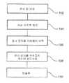
도 6은 본 발명의 일 실시예에 따른 지문 인식 모듈 제조 방법의 전반적인 단계를 개략적으로 나타낸 흐름도이다.
도 7a 내지 도 7g는 본 발명의 일 실시예에 따른 스마트 카드 제조 방법을 개략적으로 도시한 것이다.These and other aspects of the invention are described in more detail with reference to the accompanying drawings, which illustrate exemplary embodiments of the invention.
1 schematically illustrates a smart card according to an embodiment of the present invention.
2 schematically illustrates a fingerprint recognition module according to an embodiment of the present invention.
3 schematically illustrates a fingerprint recognition module according to an embodiment of the present invention.
4 schematically illustrates a fingerprint recognition module according to an embodiment of the present invention.
5 schematically illustrates a fingerprint recognition module according to an embodiment of the present invention.
6 is a flowchart schematically illustrating overall steps of a method for manufacturing a fingerprint recognition module according to an embodiment of the present invention.
7a to 7g schematically illustrate a smart card manufacturing method according to an embodiment of the present invention.
본 발명의 상세한 설명에서, 본 발명에 따른 모듈 및 방법의 다양한 실시예는 용량성 지문 센서를 포함하는 지문 인식 모듈을 참조로 주로 설명된다. 더욱이, 지문 인식 모듈은 스마트 카드에 통합을 참조하여 설명된다. 그러나, 설명된 모듈은 또한 소비자 전자장치, IoT(Internet-of-things) 및 자동차 애플리케이션과 같은 다른 애플리케이션에서의 사용에 매우 적합할 수 있다.In the detailed description of the present invention, various embodiments of modules and methods according to the present invention are described primarily with reference to a fingerprint recognition module comprising a capacitive fingerprint sensor. Furthermore, the fingerprint recognition module is described with reference to integration into a smart card. However, the described module may also be well suited for use in other applications such as consumer electronics, Internet-of-things (IoT) and automotive applications.
도 1은 본 발명의 일 실시예에 따른 지문 인식 모듈(2)을 포함하는 스마트 카드(1)를 개략적으로 도시한다.1 schematically shows a smart card 1 comprising a
도 2는 장치(20)의 제 1 면(22) 상에 배치된 감지 어레이(21)를 갖는 지문 센서 장치(20)를 포함하는 지문 인식 모듈(2)을 개략적으로 도시한 것이다. 감지 어레이(21)는 각 감지소자와 인식 모듈(2)의 감지면 상에 놓인 손가락 간에 정전용량성 결합을 감지하도록 구성된, 지문 감지소자들의 어레이, 본 명세서에서는 전기 도전 플레이트를 포함한다. 지문 센서 장치(20)는 상기 지문 센서 장치(20)를 외부 회로(미도시)에 연결하기 위한 연결 패드(24)를 더 포함한다. 외부 회로는 예를 들어 스마트 카드의 집적회로일 수 있다.FIG. 2 schematically shows a
지문 인식 모듈(2)은 지문 센서 장치(21)를 덮도록 배치된 지문 센서 장치 커버 구조물(30)을 더 포함한다. 커버 구조물은 손가락으로 접촉하도록 구성되고 이로써 인식 모듈(2)의 감지면(32)을 형성하는 제 1 면(32)과, 감지 어레이(21)를 대면한 제 2 면(35)을 갖는다. 또한, 커버 구조물은 지문 센서 모듈(2)을 외부 회로에 전기적으로 연결하기 위해 커버 구조물(30)의 제 2 면(34) 상에 배치된 도전성 트레이스(35)를 포함한다. 도 2에서 알 수 있는 바와 같이, 커버 구조물(30)의 표면적은 센서 장치(20)의 표면적보다 크므로, 인식 모듈(2)의 도전성 트레이스(35)는 감지면(32)과 동일한 방향을 바라보는 면의 대응 연결 패드에 연결될 수 있다. 마지막으로, 지문 인식 모듈(2)은 지문 감지 장치(20)의 연결 패드(24)를 커버 구조물(30)의 도전성 트레이스(35)에 전기적으로 연결하는 와이어 본드(40)를 더 포함한다. 여기서, 연결 패드(24)는 센서 기판(50)을 통해 공도 연결부(52)에 의해 감지 어레이(21) 및 관련된 감지 및 판독 회로에 전기적으로 연결된 센서 장치(20)의 제 2 면(23) 상에 배치된다.The
예시된 실시예에서, 종래의 지문 감지 장치가 사용될 수 있으며, 기존의 후면 연결부는 커버 구조물의 도전성 트레이스(35)에 와이어 본딩을 위해 사용될 수 있다. 또한, 도 2에 도시된 인식 모듈(2)에서, 감지 어레이(21)는 인식 모듈의 외부면(32), 즉 감지면에 매우 가깝고, 이는 차례로 감지면 상에 놓인 손가락과 감지 어레이(21)의 감지소자들 간에 양호한 정전용량성 결합을 야기한다. 스마트 카드에서, 커버 구조물(30)은 얇게 제조될 수 있는 반면, 글래스 아래 적용을 위해, 예를 들어 지문 센서가 디스플레이 유리 아래에 배치되는 경우, 글래스 두께는 바람직하게는 적어도 300㎛이다. 비교해 보면, 현재의 ISO 표준에 따르면, 스마트 카드의 전체 두께는 760㎛가 되어야 한다. In the illustrated embodiment, a conventional fingerprint sensing device may be used, and an existing rear connection may be used for wire bonding to the
도 3은 본 발명의 일 실시예에 따른 지문 인식 모듈(2)을 개략적으로 도시한 것이다. 도 2를 참조로 상술한 구성부품에 추가하여, 도 3의 지문 인식 모듈(2)은 커버 구조물(30)의 제 2 면(34)에 배치되고 상기 커버 구조물(30)의 도전성 트레이스(35)에 전기 연결된 수동 구성부품(70)을 더 포함한다. 하나 이상의 수동 구성부품(70)은 개별 구성부품으로서, 캡슐로서 또는 통합된 수동 장치(IPD:s)로서 커버 구조물(30) 상에 직접 배치될 수 있다.3 schematically illustrates a
더욱이, 도 3은 지문 감지 장치(20)의 제 2 면(23)에 부착된 지문 센서 제어 장치(80)를 도시하며, 제 2 면(23)은 제 1 면(22)과 반대이다. 지문 센서 제어 장치(80)는 본드 와이어(82)에 의해 커버 구조물(30)의 도전성 트레이스(35)에 연결된다. 여기에 미도시된 부가적인 옵션은 제어 장치의 배면에 수동 구성부품을 배치하고, 상기 수동 구성부품을 커버 구조물(30)의 도전성 트레이스(35) 아래의 와이어 본딩에 의해 외부 회로에 연결하는 것이다.Moreover, FIG. 3 shows the fingerprint
도 4는 지문 센서 장치(20)의 연결 패드(24)가 지문 센서 장치(20)의 제 1 면(22) 상에 배치된 본 발명의 실시예에 따른 지문 인식 모듈(2)을 개략적으로 도시한 것이다. 도시된 실시예에서, 지문 센서 장치(20)는 상기 지문 센서 장치(20)의 제 2 면(23)에 부착된 제 1 면(61)을 갖는 캐리어(60) 상에 배치된다. 캐리어(60)는 예를 들어 가요성 기판 또는 PCB일 수 있다. 지문 센서 장치(20)는 상기 지문 센서 장치(20)의 연결 패드(24)로부터 와이어 본드(64)를 통해 캐리어(60)의 제 1 면에 연결된다. 그런 후, 전기 연결부(65)가 캐리어(60)를 통해 그리고 제 1 면(61)의 반대편에 있는 캐리어(60)의 제 2 면과 도전성 트레이스(35) 사이에 연결된 와이어 본드(66)에 의해 커버 구조물(30)의 도전성 트레이스(35) 상에 더 형성된다.4 schematically shows a
도 5의 지문 인식 모듈은 도 4에 도시된 모듈과 대체로 유사하다. 차이점은 추가층(84)이 캐리어(60)와 지문 제어 장치(80) 사이에 위치한다는 것이다. 일 실시예에서, 추가층(84)은 2개의 장치들(20, 80) 사이에서 신호들을 보내는데 사용될 수 있는 실리콘 인터포저층(84)을 포함할 수 있으며, 또한 집적된 수동 구성부품들을 포함할 수 있다. 인터포저층(84)은 인터포저를 커버 구조물(30)에 연결하는 와이어 본드(85)를 포함하는 것으로 도시된다. 다른 실시예에서, 인터포저층(84)은 모듈의 디바이스를 보호하는 기계적 지지층일 수 있으며, 이 경우, 와이어 본딩이 필요없다. 지문 센서 장치(20) 및 지문 센서 제어 장치(80)의 회로는 전형적으로 실리콘으로 제조되며, 실리콘은 충분히 얇은 층에서 가요성일 수 있지만 일반적으로 강체 재료이다. 그러나, 기계적 지지층에 의해, 실리콘 장치는 파손되지 않고 부가적인 유연성을 달성할 수 있다.The fingerprint recognition module of FIG. 5 is generally similar to the module shown in FIG. 4 . The difference is that the
도 6은 본 발명의 일 실시예에 따른 지문 인식 모듈 제조 방법의 일반적인 단계를 개략적으로 나타낸 흐름도이다. 이 방법은 지문 인식 모듈(2)의 실시예를 도시한 도 2를 참조로 설명될 것이다. 상기 방법은 지문 센서 장치(20)를 제공하는 단계(102)와 외부 회로에 지문 인식 모듈(2)을 전기 연결하기 위한 도전성 트레이스를 포함한 지문 센서 장치 커버 구조물(30)를 제공하는 단계(104)를 포함한다. 다음으로, 지문 센서 장치(20)는 커버 구조물(30)에 부착되고 지문 센서 장치(20)의 연결 패드(24)와 커버 구조물(30)의 도전성 트레이스(35) 사이의 와이어 본딩(108)에 의해 상기 지문 센서 장치(20)에 전기적으로 연결된다. 최종 단계에서, 본드 와이어 및 장치를 보호하기 위해 와이어 본드(82, 85)를 포함하는 모듈(2)의 측면이 캡슐화된다(110).6 is a flowchart schematically illustrating general steps of a method for manufacturing a fingerprint recognition module according to an embodiment of the present invention. This method will be explained with reference to FIG. 2 showing an embodiment of the
도 7a 내지 도 7g는 본 명세서에 설명된 실시예 중 어느 하나에 따른 지문 인식 모듈을 포함하는 스마트 카드를 제조하는 방법을 개략적으로 도시한 것이다.7a to 7g schematically illustrate a method of manufacturing a smart card including a fingerprint recognition module according to any one of the embodiments described herein.
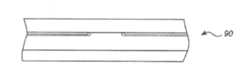
도 7a는 복수의 층들을 포함하는 라미네이트 스마트 카드 기판(90)을 도시한 것이다. 스마트 카드를 형성하는 것은 스마트 카드 기판(90)의 상부층을 밀링 및 드릴링하여 오목부(91)를 형성하는 것을 포함한다. 오목부(90)는 상부(92) 및 하부(93)를 포함하며, 상부(92) 면적이 하부(93) 면적보다 크고, 이로써 T자형 오목부가 형성된다.7A shows a laminate
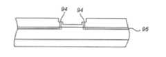
도 7c는 오목부(92)의 상부로부터 스마트 카드 기판의 도전층(95)까지 드릴링된 개구(94)를 도시한 것이다. 스마트 카드는 실제로 복수의 층을 포함할 수 있다. 그러나, 간략히 하기 위해, 단 하나의 도전층만이 도시되어 있다. 스마트 카드의 도전층(들)은 지문 인식 모듈(2)을 스마트 카드의 집적회로에 연결하기 위한 도전성 트레이스를 포함한다.7C shows an
도 7d에서, 도전성 재료는 개구(94) 내에 배치되어 도전층(95)에 도전성 공도 연결부(96)를 형성한다.In FIG. 7D , a conductive material is disposed in the
도 7e는 오목부(91)의 T자형에 대응하는 T자형을 갖는 인식 모듈(2)을 제공하는 단계를 도시한 것이고, 도 7f에서, 인식 모듈은 오목부 내에 배열된다. 특히, 커버 구조물(30)의 도전성 트레이스(35)는 스마트 카드의 공도 연결부(96)와 전기 연결을 형성하도록 위치된다. 지문 인식 모듈(2)은 공도 연결부(96)의 위치에서 도전성 접착제(97)를 사용하여 스마트 카드 기판(90)에 부착되는 것이 유리하다.Fig. 7E shows the step of providing the
최종 단계에서, 도 7d에 도시된 바와 같이, 접착제를 경화시키기 위해 가열 도구(98)를 사용하여 접착제(97)가 가열된다. 도전성 접착제를 사용하는 대신에, 저온 솔더 재료를 사용할 수도 있는데, 솔더링 온도는 스마트 카드 기판의 용융을 방지할 정도로 충분히 낮다.In a final step, as shown in Figure 7d, the adhesive 97 is heated using a
본 명세서에 설명된 지문 인식 모듈의 다양한 실시예는 하나의 제어 장치, 하나의 수동 구성부품 등을 포함한다. 그러나, 당업자는 기술된 모듈이 설명된 여러 가지 장치 및 구성부품 중 2 이상을 동등하게 잘 포함할 수 있음을 쉽게 알 수 있다.Various embodiments of the fingerprint identification module described herein include one control device, one passive component, and the like. However, one skilled in the art will readily appreciate that a described module may equally well include two or more of the various devices and components described.
더욱이, 비록 특정 예시적인 실시예를 참조로 본 발명을 설명하였으나, 많은 상이한 변경, 수정 등이 당업자에게 명백해질 것이다. 또한, 모듈, 스마트 카드 및 방법의 일부는 생략, 상호 교환 또는 다양한 방식으로 배열될 수 있고, 모듈, 스마트 카드 및 방법이 본 발명의 기능을 수행할 수 있음을 알아야 한다.Moreover, although the present invention has been described with reference to specific exemplary embodiments, many different alterations, modifications, etc. will become apparent to those skilled in the art. It should also be appreciated that some of the modules, smart cards and methods may be omitted, interchanged or arranged in a variety of ways, and the modules, smart cards and methods may perform the functions of the present invention.
또한, 개시된 실시예에 대한 변형은 도면, 명세서 및 청구범위의 연구로부터 청구된 발명을 실시하는 당업자에 의해 이해되고 달성될 수 있다. 청구범위에서, "포함하는"이라는 단어는 다른 요소 또는 단계를 배제하지 않으며, 부정관사 "a" 또는 "an"은 복수를 배제하지 않는다. 특정 측정값이 서로 다른 종속항에 인용되어 있다는 단순한 사실만으로 이 측정 값의 조합을 활용할 수 없다는 것을 의미하지는 않다.Further, modifications to the disclosed embodiments may be understood and effected by those skilled in the art practicing the claimed invention from a study of the drawings, specification, and claims. In the claims, the word "comprising" does not exclude other elements or steps, and the indefinite article "a" or "an" does not exclude a plurality. The mere fact that a particular measure is recited in mutually different dependent claims does not mean that a combination of these measures cannot be utilized.
Claims (21)
Translated fromKorean상기 지문 센서 장치를 덮도록 배치되고, 손가락으로 접촉하도록 구성되며 이로써 인식 모듈의 감지면을 형성하는 제 1 면(32)과 상기 감지 어레이를 바라보는 제 2 면(34)을 갖는 지문 센서 장치 커버 구조물(30)을 포함하고,
상기 지문 센서 장치는 상기 지문 센서 장치를 외부 회로에 연결하기 위한 연결 패드(24)를 포함하며,
상기 커버 구조물은 상기 지문 센서 모듈을 외부 회로에 전기 연결하기 위해 상기 커버 구조물의 제 2 면 상에 배치된 도전성 트레이스(35)를 포함하고, 상기 커버 구조물의 표면적은 상기 센서 장치의 표면적보다 더 크며,
상기 지문 센서 장치는 상기 지문 감지 장치의 상기 연결 패드를 상기 커버 구조물의 상기 도전성 트레이스에 전기적으로 연결하는 와이어 본드(40, 66)를 더 포함하고,
상기 연결 패드는 상기 제 1 면(22)의 맞은 편에 있는 상기 지문 센서 장치의 제 2 면(23) 상에 배치되고, 상기 지문 센서 장치는 상기 지문 센서 장치의 상기 제 1 면으로부터 상기 지문 센서 장치의 상기 제 2 면의 상기 연결 패드에 이르는 공도 연결부(52)를 포함하는 기판(50)을 더 포함하는, 지문 인식 모듈(2).a fingerprint sensor device (20) having a sensing array (21) disposed on a first side (22) of the device and comprising an array of fingerprint sensing elements; and
a fingerprint sensor device cover disposed to cover the fingerprint sensor device and configured to be contacted by a finger, thereby having a first face (32) forming a sensing face of a recognition module and a second face (34) facing the sensing array; Including the structure 30,
The fingerprint sensor device includes a connection pad 24 for connecting the fingerprint sensor device to an external circuit,
the cover structure includes a conductive trace (35) disposed on a second side of the cover structure for electrically connecting the fingerprint sensor module to an external circuit, the surface area of the cover structure being greater than the surface area of the sensor device; ,
the fingerprint sensor device further comprises a wire bond (40, 66) electrically connecting the connection pad of the fingerprint sensing device to the conductive trace of the cover structure;
The connection pad is disposed on a second side 23 of the fingerprint sensor device opposite the first side 22, and the fingerprint sensor device connects to the fingerprint sensor device from the first side of the fingerprint sensor device. The fingerprint recognition module (2) further comprising a substrate (50) comprising a public road connection (52) leading to the connection pad of the second side of the device.
상기 연결 패드는 상기 지문 센서 장치의 상기 제 1 면에 배치되고,
상기 지문 센서 장치는:
상기 지문 센서 장치의 상기 제 2 면에 부착된 제 1 면(61)을 갖는 캐리어(60);
상기 지문 센서 장치의 상기 연결 패드와 상기 캐리어의 상기 제 1 면 사이에 와이어 본드(64); 및
상기 제 1 면의 맞은 편에 있는 상기 캐리어의 제 2 면과 상기 커버 구조물의 도전성 트레이스 사이에 배열된 와이어 본드(66)를 더 포함하는 지문 인식 모듈.According to claim 1,
the connection pad is disposed on the first surface of the fingerprint sensor device;
The fingerprint sensor device:
a carrier (60) having a first side (61) attached to the second side of the fingerprint sensor device;
a wire bond (64) between the connection pad of the fingerprint sensor device and the first side of the carrier; and
and a wire bond (66) disposed between a conductive trace of the cover structure and a second side of the carrier opposite the first side.
상기 센서 장치와 상기 커버 구조물 사이에 배치된 몰드층(68)을 더 포함하는 지문 인식 모듈.According to claim 1,
The fingerprint recognition module further comprises a mold layer (68) disposed between the sensor device and the cover structure.
상기 커버 구조물은 도전성 트레이스를 손상시키는 적어도 하나의 층과 적어도 하나의 절연층을 포함한 라미네이트 구조물인 지문 인식 모듈.According to claim 1,
The fingerprint recognition module of claim 1 , wherein the cover structure is a laminate structure including at least one layer that damages a conductive trace and at least one insulating layer.
상기 커버 구조물의 상기 제 2 면(34) 상에 배치되고 상기 커버 구조물의 도전성 트레이스들에 전기적으로 연결된 수동 구성부품(70)을 더 포함하는 지문 인식 모듈.According to claim 1,
and a passive component (70) disposed on the second side (34) of the cover structure and electrically connected to the conductive traces of the cover structure.
상기 캐리어의 상기 제 1 면(61) 상에 배치되고 상기 커버 구조물의 도전 트레이스들에 전기적으로 연결된 수동 구성부품(70)을 더 포함하는 지문 인식 모듈.According to claim 3,
and a passive component (70) disposed on the first side (61) of the carrier and electrically connected to the conductive traces of the cover structure.
상기 지문 감지 장치의 제 2 면에 부착된 지문 센서 제어 장치(80)를 더 포함하고, 상기 제 2 면은 상기 제 1 면의 맞은 편에 있는 지문 인식 모듈.According to claim 1,
and a fingerprint sensor control device (80) attached to a second side of the fingerprint sensing device, wherein the second side is opposite the first side.
상기 지문 센서 제어 장치를 상기 커버 구조물의 도전성 트레이스에 전기적으로 연결하는 와이어 본드(82)를 더 포함하는 지문 인식 모듈.According to claim 8,
and a wire bond (82) electrically connecting the fingerprint sensor control device to a conductive trace of the cover structure.
상기 지문 센서 제어 장치와 상기 지문 인식 모듈의 제 2 면 사이에 배치된 실리콘 인터포저층(84)을 더 포함하는 지문 인식 모듈.According to claim 8,
The fingerprint recognition module further comprises a silicon interposer layer (84) disposed between the fingerprint sensor control device and the second surface of the fingerprint recognition module.
상기 감지면 상에 배치된 손가락과 상기 지문 인식 모듈의 구동 신호 회로 사이에 전기적 연결을 제공하기 위해 상기 감지 어레이에 인접하게 배치된 전기 도전성 베젤을 더 포함하는 지문 인식 모듈.According to claim 1,
and an electrically conductive bezel disposed adjacent to the sensing array to provide an electrical connection between a finger disposed on the sensing surface and a drive signal circuit of the fingerprint recognition module.
상기 커버 구조물은 상기 지문 센서 모듈이 T자형 프로파일을 갖도록 상기 지문 센서 장치의 외부로 뻗어 있는 지문 인식 모듈.According to claim 1,
The cover structure extends outside the fingerprint sensor device so that the fingerprint sensor module has a T-shaped profile.
상기 커버 구조물은 가요성인 지문 인식 모듈.According to claim 1,
The fingerprint recognition module of claim 1 , wherein the cover structure is flexible.
보안 요소를 더 포함하는 지문 인식 모듈.According to claim 1,
A fingerprint recognition module further comprising a secure element.
상기 스마트 카드는 상기 지문 인식 모듈이 배치되는 오목부를 포함하고;
상기 지문 인식 모듈의 상기 커버 구조물은 상기 도전성 트레이스를 상기 스마트 카드의 도전성 인레이의 대응 연결 패드에 연결하기 위한 연결 패드를 포함하는 스마트 카드.A smart card (1) comprising a fingerprint identification module (10) according to any one of claims 1 and 3 to 14,
the smart card includes a concave portion in which the fingerprint recognition module is disposed;
and the cover structure of the fingerprint recognition module includes connection pads for connecting the conductive traces to corresponding connection pads of the conductive inlay of the smart card.
상기 오목부는 상기 지문 인식 모듈의 형상과 일치하는 형상을 갖는 스마트 카드.According to claim 15,
The smart card of claim 1 , wherein the concave portion has a shape matching a shape of the fingerprint recognition module.
상기 오목부는 T자 형상이고 대응하는 T자형 지문 인식 모듈을 수용하도록 구성된 스마트 카드.According to claim 15,
The smart card according to claim 1 , wherein the concave portion is T-shaped and configured to receive a corresponding T-shaped fingerprint identification module.
지문 인식 모듈을 외부 회로에 전기 연결하기 위해, 커버 구조물의 제 2 면 상에 배치된 도전성 트레이스를 포함하는 지문 센서 장치 커버 구조물을 제공하는 단계;
상기 지문 센서 장치를 상기 커버 구조물에 부착하는 단계; 및
상기 연결 패드와 상기 도전성 트레이스 사이의 와이어 본딩에 의해 상기 지문 센서 장치를 전기적으로 연결하는 단계를 포함하며,
상기 연결 패드는 상기 제 1 면(22)의 맞은 편에 있는 상기 지문 센서 장치의 제 2 면(23) 상에 배치되고, 상기 지문 센서 장치는 상기 지문 센서 장치의 상기 제 1 면으로부터 상기 지문 센서 장치의 상기 제 2 면의 상기 연결 패드에 이르는 공도 연결부(52)를 포함하는 기판(50)을 더 포함하는, 지문 인식 모듈을 제조하는 방법.providing a fingerprint sensor device (20) having a sensing array disposed on a first side (22) of the device and comprising an array of fingerprint sensing elements, the fingerprint sensor device (20) comprising the fingerprint sensor device (20) providing a fingerprint sensor device (20) comprising a connection pad (24) for connecting to an external circuit;
providing a fingerprint sensor device cover structure comprising a conductive trace disposed on a second side of the cover structure for electrically connecting the fingerprint recognition module to external circuitry;
attaching the fingerprint sensor device to the cover structure; and
electrically connecting the fingerprint sensor device by wire bonding between the connection pad and the conductive trace;
The connection pad is disposed on a second side 23 of the fingerprint sensor device opposite the first side 22, and the fingerprint sensor device connects to the fingerprint sensor device from the first side of the fingerprint sensor device. and a substrate (50) comprising a public road connection (52) leading to the connection pad of the second side of the device.
상기 지문 인식 모듈의 제 2 면에 지문 센서 제어 장치를 부착하는 단계를 더 포함하고, 상기 제 2 면은 상기 제 1 면의 맞은 편에 있는 지문 인식 모듈을 제조하는 방법.According to claim 18,
and attaching a fingerprint sensor control device to a second side of the fingerprint recognition module, wherein the second side is opposite the first side.
상기 지문 인식 모듈을 캡슐화하는 단계를 더 포함하는 지문 인식 모듈을 제조하는 방법.According to claim 18 or 19,
The method of manufacturing a fingerprint recognition module further comprising the step of encapsulating the fingerprint recognition module.
복수의 층을 포함하는 스마트 카드 기판을 제공하는 단계;
하부 및 상부를 포함하며 상기 상부 면적이 상기 하부 면적보다 큰 오목부를 상기 스마트 카드에 형성하는 단계;
상기 오목부의 상부와 상기 스마트 카드의 도전성 트레이스 사이에 공도 연결부를 형성하는 단계; 및
커버층의 상기 도전성 트레이스가 상기 공도 연결부와의 전기 접촉을 형성하도록 상기 오목부 내에 인식 모듈을 배치하는 단계를 포함하는 스마트 카드 제조 방법.A smart card manufacturing method comprising the fingerprint recognition module according to any one of claims 1 and 3 to 14,
providing a smart card substrate comprising a plurality of layers;
forming a concave portion in the smart card, including a lower portion and an upper portion, wherein the upper area is larger than the lower area;
forming a public road connection between an upper portion of the concave portion and a conductive trace of the smart card; and
and positioning a recognition module within the recess such that the conductive trace of the cover layer makes electrical contact with the airway connection.
Applications Claiming Priority (3)
| Application Number | Priority Date | Filing Date | Title |
|---|---|---|---|
| SE1651654 | 2016-12-15 | ||
| SE1651654-4 | 2016-12-15 | ||
| PCT/SE2017/051210WO2018111174A1 (en) | 2016-12-15 | 2017-12-04 | Fingerprint sensing module and method for manufacturing the fingerprint sensing module |
Publications (2)
| Publication Number | Publication Date |
|---|---|
| KR20190096977A KR20190096977A (en) | 2019-08-20 |
| KR102468554B1true KR102468554B1 (en) | 2022-11-18 |
Family
ID=60781507
Family Applications (1)
| Application Number | Title | Priority Date | Filing Date |
|---|---|---|---|
| KR1020197014898AActiveKR102468554B1 (en) | 2016-12-15 | 2017-12-04 | Fingerprint recognition module and manufacturing method of the fingerprint recognition module |
Country Status (6)
| Country | Link |
|---|---|
| US (1) | US10395164B2 (en) |
| EP (2) | EP3336759B1 (en) |
| JP (2) | JP7065094B2 (en) |
| KR (1) | KR102468554B1 (en) |
| CN (2) | CN207601824U (en) |
| WO (1) | WO2018111174A1 (en) |
Families Citing this family (32)
| Publication number | Priority date | Publication date | Assignee | Title |
|---|---|---|---|---|
| US20180165495A1 (en)* | 2016-12-09 | 2018-06-14 | Fingerprint Cards Ab | Electronic device |
| US11610429B2 (en) | 2016-12-15 | 2023-03-21 | Fingerprint Cards Anacatum Ip Ab | Fingerprint sensing module and method for manufacturing the fingerprint sensing module |
| US11023702B2 (en) | 2016-12-15 | 2021-06-01 | Fingerprint Cards Ab | Fingerprint sensing module and method for manufacturing the fingerprint sensing module |
| US10395164B2 (en)* | 2016-12-15 | 2019-08-27 | Fingerprint Cards Ab | Fingerprint sensing module and method for manufacturing the fingerprint sensing module |
| US10984304B2 (en) | 2017-02-02 | 2021-04-20 | Jonny B. Vu | Methods for placing an EMV chip onto a metal card |
| FR3069081B1 (en)* | 2017-07-17 | 2021-08-20 | Safran Identity & Security | ELECTRONIC CARD INCLUDING A FOOTPRINT SENSOR AND METHOD FOR MANUFACTURING SUCH A CARD |
| CN109075137B (en)* | 2017-07-20 | 2022-03-01 | 深圳市汇顶科技股份有限公司 | Chip packaging structure, chip module and electronic terminal |
| US10509936B2 (en)* | 2017-08-28 | 2019-12-17 | Superc-Touch Corporation | Fingerprint identification apparatus having conductive structure |
| US20200051938A9 (en)* | 2017-12-18 | 2020-02-13 | China Wafer Level Csp Co., Ltd. | Fingerprint chip packaging method and fingerprint chip package |
| TWI705538B (en)* | 2018-06-29 | 2020-09-21 | 同欣電子工業股份有限公司 | Manufacturing method of fingerprint sensing package module |
| USD956760S1 (en)* | 2018-07-30 | 2022-07-05 | Lion Credit Card Inc. | Multi EMV chip card |
| CN109496315B (en)* | 2018-10-26 | 2022-05-03 | 深圳市汇顶科技股份有限公司 | Fingerprint detection coding device, fingerprint detection system and electronic equipment |
| SG10201902933WA (en)* | 2019-04-01 | 2020-11-27 | Advanide Holdings Pte Ltd | An improved card with fingerprint biometrics |
| FR3095287B1 (en) | 2019-04-19 | 2022-11-04 | Linxens Holding | Biometric sensor module for smart card and method of manufacturing such a module |
| FR3095285B1 (en) | 2019-04-19 | 2022-11-11 | Linxens Holding | Biometric sensor module for smart card and method of manufacturing such a module |
| FR3095536B1 (en) | 2019-04-25 | 2021-09-24 | Idemia Identity & Security France | Microcircuit card module with fingerprint sensor and protective shell |
| KR102138671B1 (en)* | 2019-05-14 | 2020-08-11 | (주)비티비엘 | Smart card with improved biosensor site |
| US20210081743A1 (en) | 2019-08-12 | 2021-03-18 | Federal Card Services, LLC | Dual interface metal cards and methods of manufacturing |
| US12277462B2 (en) | 2019-08-14 | 2025-04-15 | Federal Card Services, LLC | Metal-containing dual interface smartcards |
| US11113593B2 (en) | 2019-08-15 | 2021-09-07 | Federal Card Services; LLC | Contactless metal cards with fingerprint sensor and display |
| CN110458143B (en)* | 2019-08-21 | 2022-04-15 | 京东方科技集团股份有限公司 | Fingerprint identification device, fingerprint identification method and electronic equipment |
| US11341385B2 (en) | 2019-11-16 | 2022-05-24 | Federal Card Services, LLC | RFID enabled metal transaction card with shaped opening and shaped slit |
| EP3836010B1 (en)* | 2019-12-12 | 2024-07-24 | Fingerprint Cards Anacatum IP AB | A biometric sensor module for card integration |
| US11055683B1 (en)* | 2020-04-02 | 2021-07-06 | Capital One Services, Llc | Computer-based systems involving fingerprint or biometrically-activated transaction cards and methods of use thereof |
| FR3111215B1 (en)* | 2020-06-04 | 2022-08-12 | Linxens Holding | Biometric sensor module for smart card and method of manufacturing such a module |
| EP3933697B1 (en)* | 2020-07-01 | 2022-06-15 | Fingerprint Cards Anacatum IP AB | Biometric imaging module and method for manufacturing a biometric imaging module |
| US11948033B2 (en) | 2020-10-23 | 2024-04-02 | Visa International Service Association | Integrated biometric sensor and memory for biometric card |
| SE2051294A1 (en) | 2020-11-06 | 2022-05-07 | Fingerprint Cards Anacatum Ip Ab | Integrated biometric sensor module and method for manufacturing a smartcard comprising an integrated biometric sensor module |
| KR20240018865A (en) | 2022-08-03 | 2024-02-14 | 삼성전자주식회사 | Fingerprint sensor package and smart card having the same |
| WO2024049340A1 (en)* | 2022-08-29 | 2024-03-07 | Fingerprint Cards Anacatum Ip Ab | Biometric imaging device and method for manufacturing the biometric imaging device |
| FR3144885A1 (en) | 2023-01-09 | 2024-07-12 | Linxens Holding | Reinforced smart card module and method of manufacturing such a smart card |
| KR102758876B1 (en)* | 2023-09-27 | 2025-01-23 | 주식회사 이터널 | Power supply film and Method for user's fingerprint registering of fingerprint recognition card |
Citations (2)
| Publication number | Priority date | Publication date | Assignee | Title |
|---|---|---|---|---|
| US20150049925A1 (en)* | 2012-04-24 | 2015-02-19 | Zwipe, As | Method of Manufacturing an Electronic Card |
| US20160335470A1 (en)* | 2015-05-12 | 2016-11-17 | Amkor Technology, Inc. | Fingerprint sensor and manufacturing method thereof |
Family Cites Families (33)
| Publication number | Priority date | Publication date | Assignee | Title |
|---|---|---|---|---|
| JP3769332B2 (en)* | 1996-09-13 | 2006-04-26 | 大日本印刷株式会社 | IC card manufacturing method |
| DE19921231A1 (en) | 1999-05-07 | 2000-11-09 | Giesecke & Devrient Gmbh | Fingerprint sensor for chip card identification has sensor segments supported by elastically compressible support pad for allowing detection of full fingerprint |
| FR2797075B1 (en) | 1999-07-26 | 2001-10-12 | Gemplus Card Int | METHOD FOR MANUFACTURING A PORTABLE DEVICE WITH INTEGRATED CIRCUITS, OF THE SMART CARD TYPE OF REDUCED FORMAT IN RELATION TO THE STANDARD FORMAT |
| JP2004509479A (en) | 2000-09-19 | 2004-03-25 | ナノピアス・テクノロジーズ・インコーポレイテッド | Method for assembling a plurality of components and a plurality of antennas in a radio frequency identification device |
| NO316776B1 (en)* | 2001-12-07 | 2004-05-03 | Idex Asa | Package solution for fingerprint sensor |
| DE10221214A1 (en) | 2002-05-13 | 2003-11-27 | Orga Kartensysteme Gmbh | Integrated circuit module is embedded into a plastic smart card and has interconnected chips on a common carrier set into protective material |
| US6924496B2 (en)* | 2002-05-31 | 2005-08-02 | Fujitsu Limited | Fingerprint sensor and interconnect |
| CZ2005209A3 (en) | 2002-09-10 | 2005-12-14 | Ivi Smart Technologies, Inc. | Secure Biometric Identity Verification |
| JP4904769B2 (en)* | 2005-10-21 | 2012-03-28 | 富士通セミコンダクター株式会社 | Semiconductor device |
| CN100590643C (en)* | 2007-01-17 | 2010-02-17 | 南茂科技股份有限公司 | Film packaging structure of fingerprint identifier |
| JP2010122015A (en)* | 2008-11-18 | 2010-06-03 | Fujitsu Ltd | Sensor unit and method for manufacturing electronic apparatus |
| NO20093601A1 (en) | 2009-12-29 | 2011-06-30 | Idex Asa | surface Sensor |
| EP2558978B1 (en)* | 2010-04-15 | 2016-06-29 | Apple Inc. | Finger sensor including capacitive lens and associated methods |
| US8736001B2 (en)* | 2010-06-18 | 2014-05-27 | Authentec, Inc. | Finger sensor including encapsulating layer over sensing area and related methods |
| US8717775B1 (en)* | 2010-08-02 | 2014-05-06 | Amkor Technology, Inc. | Fingerprint sensor package and method |
| KR20120019729A (en)* | 2010-08-26 | 2012-03-07 | (주)바이오스마트 | Ic card constructed by using spot welding and method the same |
| JP5069342B2 (en)* | 2010-09-01 | 2012-11-07 | エイエスディ株式会社 | IC card with fingerprint reading sensor and manufacturing method thereof |
| US9158958B2 (en)* | 2010-10-28 | 2015-10-13 | Synaptics Incorporated | Signal strength enhancement in a biometric sensor array |
| AP2015008710A0 (en)* | 2013-01-29 | 2015-08-31 | Mary Grace | Smart card and smart card system with enhanced security features |
| WO2015013530A1 (en)* | 2013-07-24 | 2015-01-29 | Synaptics Incorporated | Signal strength enhancement in a biometric sensor array |
| KR101773029B1 (en)* | 2013-08-23 | 2017-08-30 | 핑거프린트 카드즈 에이비 | Connection pads for a fingerprint sensing device |
| TWI534962B (en)* | 2013-12-09 | 2016-05-21 | 茂丞科技股份有限公司 | Proximity sensor with hidden couple electrode and method of manufacturing such sensor |
| DE102013113901B3 (en)* | 2013-12-12 | 2015-01-08 | Innenministerium des Landes Schleswig-Holstein, vertreten durch den Innenminister | Method of visualizing fingerprints |
| US9520697B2 (en)* | 2014-02-10 | 2016-12-13 | Soraa Laser Diode, Inc. | Manufacturable multi-emitter laser diode |
| TWI530885B (en)* | 2014-03-18 | 2016-04-21 | 茂丞科技股份有限公司 | All-flat sensor with exposed colorful member and electronic device using such sensor |
| US9576177B2 (en)* | 2014-12-11 | 2017-02-21 | Fingerprint Cards Ab | Fingerprint sensing device |
| US9449212B2 (en)* | 2014-12-22 | 2016-09-20 | Fingerprint Cards Ab | Capacitive fingerprint sensor with sensing elements comprising timing circuitry |
| TWI594341B (en)* | 2015-01-19 | 2017-08-01 | 神盾股份有限公司 | Fingerprint sensor package and method for fabricating the same |
| TW201643772A (en) | 2015-06-08 | 2016-12-16 | 指紋卡公司 | Fingerprint sensing device with interposer structure |
| CN204808272U (en)* | 2015-07-03 | 2015-11-25 | 宸鸿科技(厦门)有限公司 | Touch panel with fingerprint identification function |
| TWM523147U (en)* | 2015-09-10 | 2016-06-01 | Metrics Technology Co Ltd J | Fingerprint sensor and fingerprint sensing module |
| US9792516B2 (en)* | 2016-01-26 | 2017-10-17 | Next Biometrics Group Asa | Flexible card with fingerprint sensor |
| US10395164B2 (en)* | 2016-12-15 | 2019-08-27 | Fingerprint Cards Ab | Fingerprint sensing module and method for manufacturing the fingerprint sensing module |
- 2017
- 2017-11-09USUS15/807,679patent/US10395164B2/enactiveActive
- 2017-12-04KRKR1020197014898Apatent/KR102468554B1/enactiveActive
- 2017-12-04JPJP2019531057Apatent/JP7065094B2/enactiveActive
- 2017-12-04WOPCT/SE2017/051210patent/WO2018111174A1/ennot_activeCeased
- 2017-12-13EPEP17207037.7Apatent/EP3336759B1/enactiveActive
- 2017-12-13EPEP19180709.8Apatent/EP3564852B1/enactiveActive
- 2017-12-15CNCN201721766773.6Upatent/CN207601824U/enactiveActive
- 2017-12-15CNCN201711350145.4Apatent/CN108229340B/enactiveActive
- 2022
- 2022-04-25JPJP2022071629Apatent/JP7289956B2/enactiveActive
Patent Citations (2)
| Publication number | Priority date | Publication date | Assignee | Title |
|---|---|---|---|---|
| US20150049925A1 (en)* | 2012-04-24 | 2015-02-19 | Zwipe, As | Method of Manufacturing an Electronic Card |
| US20160335470A1 (en)* | 2015-05-12 | 2016-11-17 | Amkor Technology, Inc. | Fingerprint sensor and manufacturing method thereof |
Also Published As
| Publication number | Publication date |
|---|---|
| JP2020503606A (en) | 2020-01-30 |
| EP3336759A1 (en) | 2018-06-20 |
| JP7065094B2 (en) | 2022-05-11 |
| US20180174018A1 (en) | 2018-06-21 |
| CN108229340B (en) | 2021-07-30 |
| JP7289956B2 (en) | 2023-06-12 |
| EP3564852A1 (en) | 2019-11-06 |
| KR20190096977A (en) | 2019-08-20 |
| WO2018111174A1 (en) | 2018-06-21 |
| US10395164B2 (en) | 2019-08-27 |
| CN207601824U (en) | 2018-07-10 |
| EP3564852B1 (en) | 2023-10-18 |
| CN108229340A (en) | 2018-06-29 |
| EP3336759B1 (en) | 2019-06-19 |
| JP2022106838A (en) | 2022-07-20 |
Similar Documents
| Publication | Publication Date | Title |
|---|---|---|
| KR102468554B1 (en) | Fingerprint recognition module and manufacturing method of the fingerprint recognition module | |
| US11610429B2 (en) | Fingerprint sensing module and method for manufacturing the fingerprint sensing module | |
| US11023702B2 (en) | Fingerprint sensing module and method for manufacturing the fingerprint sensing module | |
| US11119615B2 (en) | Fingerprint sensor and button combinations and methods of making same | |
| US10055664B2 (en) | Flexible card with fingerprint sensor | |
| JP2020503606A5 (en) | ||
| US9978673B2 (en) | Package structure and method for fabricating the same | |
| CN102918546A (en) | Finger sensor including capacitive lens and related method | |
| EP3836010B1 (en) | A biometric sensor module for card integration | |
| US11455816B2 (en) | Fingerprint sensor module comprising a fingerprint sensor device and a substrate connected to the sensor device | |
| US20240161534A1 (en) | Fingerprint sensor module and method for manufacturing a fingerprint sensor module | |
| US10025969B2 (en) | Fingerprint identification module and manufacturing method thereof |
Legal Events
| Date | Code | Title | Description |
|---|---|---|---|
| PA0105 | International application | Patent event date:20190523 Patent event code:PA01051R01D Comment text:International Patent Application | |
| PG1501 | Laying open of application | ||
| PA0201 | Request for examination | Patent event code:PA02012R01D Patent event date:20200910 Comment text:Request for Examination of Application | |
| N231 | Notification of change of applicant | ||
| PN2301 | Change of applicant | Patent event date:20211230 Comment text:Notification of Change of Applicant Patent event code:PN23011R01D | |
| E902 | Notification of reason for refusal | ||
| PE0902 | Notice of grounds for rejection | Comment text:Notification of reason for refusal Patent event date:20220414 Patent event code:PE09021S01D | |
| E701 | Decision to grant or registration of patent right | ||
| PE0701 | Decision of registration | Patent event code:PE07011S01D Comment text:Decision to Grant Registration Patent event date:20221028 | |
| GRNT | Written decision to grant | ||
| PR0701 | Registration of establishment | Comment text:Registration of Establishment Patent event date:20221115 Patent event code:PR07011E01D | |
| PR1002 | Payment of registration fee | Payment date:20221116 End annual number:3 Start annual number:1 | |
| PG1601 | Publication of registration |