KR102468198B1 - Pad area electrode structure and display device having the same - Google Patents
Pad area electrode structure and display device having the sameDownload PDFInfo
- Publication number
- KR102468198B1 KR102468198B1KR1020150191773AKR20150191773AKR102468198B1KR 102468198 B1KR102468198 B1KR 102468198B1KR 1020150191773 AKR1020150191773 AKR 1020150191773AKR 20150191773 AKR20150191773 AKR 20150191773AKR 102468198 B1KR102468198 B1KR 102468198B1
- Authority
- KR
- South Korea
- Prior art keywords
- pad
- electrode
- substrate
- display area
- disposed
- Prior art date
- Legal status (The legal status is an assumption and is not a legal conclusion. Google has not performed a legal analysis and makes no representation as to the accuracy of the status listed.)
- Active
Links
Images


Classifications
- H01L51/56—
- H01L27/3225—
- H01L27/3248—
- H01L27/3258—
- H01L27/3262—
- H01L51/5203—
- H01L51/5253—
- H01L2227/32—
Landscapes
- Electroluminescent Light Sources (AREA)
- Devices For Indicating Variable Information By Combining Individual Elements (AREA)
Abstract
Translated fromKoreanDescription
Translated fromKorean본 발명은 패드부 전극 구조 및 이를 갖는 표시 장치에 관한 것이다.
The present invention relates to a pad part electrode structure and a display device having the same.
최근 들어, 음극선관(Cathode Ray Tube)의 단점인 무게와 부피를 줄일 수 있는 각종 평판 표시장치들이 개발되고 있다. 이러한 평판 표시장치는 액정표시장치(Liquid Crystal Display), 전계 방출 표시장치(Field Emission Display), 플라즈마 디스플레이 패널(Plasma Display Panel) 및 유기전계발광 표시 장치(Electro-luminescence Display Device) 등이 있다.Recently, various flat panel display devices capable of reducing the weight and volume, which are disadvantages of cathode ray tubes, are being developed. Such a flat panel display includes a liquid crystal display, a field emission display, a plasma display panel, and an electro-luminescence display device.
이러한 평판표시장치의 표시품질을 높이고 대화면화를 시도하는 연구들이 활발히 진행되고 있다. 이들 중, 플라즈마 디스플레이 패널은 구조와 제조공정이 단순하기 때문에 경박 단소하면서도 대화면화에 가장 유리한 표시장치로 주목 받고 있지만 발광효율과 휘도가 낮고 소비전력이 큰 단점이 있다. 이에 비하여, 스위칭 소자로 박막 트랜지스터(Thin Film Transistor)가 적용된 액티브 매트릭스 액정표시장치는 반도체 공정을 이용하기 때문에 대화면화가 어렵다. 또한, 백라이트 유닛으로 인하여 소비전력이 큰 단점이 있고, 편광필터, 프리즘시트, 확산판 등의 광학소자들에 의해 광손실이 많고 시야각이 좁은 단점이 있다.Researches are being actively conducted to improve the display quality of such a flat panel display and to make it larger. Among them, the plasma display panel is attracting attention as a display device that is light, thin, and compact, and is most advantageous for a large screen because of its simple structure and manufacturing process. In contrast, an active matrix liquid crystal display in which a thin film transistor is applied as a switching element is difficult to make into a large screen because it uses a semiconductor process. In addition, there is a disadvantage in that power consumption is high due to the backlight unit, and there is a disadvantage in that light loss is high and the viewing angle is narrow due to optical elements such as a polarization filter, a prism sheet, and a diffusion plate.
이에 비하여, 유기전계발광 표시 장치는 스스로 발광하는 자발광소자로서 응답속도가 빠르고 발광효율, 휘도 및 시야각이 큰 장점이 있다. 또한, 유기전계발광 표시 장치는 수십 볼트의 낮은 직류 전압에서 구동됨과 아울러, 빠른 응답속도를 가지고, 고휘도를 얻을 수 있으며 R, G, B의 다양한 색을 발광시킬 수 있다.
In contrast, the organic light emitting display device is a self-emitting device that emits light by itself, and has advantages such as fast response speed, luminous efficiency, luminance, and viewing angle. In addition, the organic light emitting display device is driven at a low DC voltage of several tens of volts, has a fast response speed, can obtain high luminance, and can emit various colors of R, G, and B.
도 1은 종래에 따른 유기전계발광 표시 장치를 나타낸 단면도이고, 도 2는 외부 보호층을 레이저 패터닝 방식으로 제거하는 과정을 설명하기 위한 모식도이다.1 is a cross-sectional view of a conventional organic light emitting display device, and FIG. 2 is a schematic diagram for explaining a process of removing an external protective layer using a laser patterning method.
도 1 및 도 2에 도시된 바와 같이, 종래에 따른 유기전계발광 표시 장치(1)는 제1 기판(10)과, 제1 기판(10)과 대향하는 제2 기판(95)을 포함한다.As shown in FIGS. 1 and 2 , a conventional organic light
이때, 제1 기판(10)은 화상을 구현하는 표시 영역(AA)과, 화상을 구현하지 않는 비표시 영역(NAA)을 갖는다. 이러한 제1 기판(10)의 재질로는 유리, 플라스틱 등이 이용될 수 있다. 그리고, 제2 기판(95)의 재질로는 유리, 플라스틱, 스테인리스 스틸(stainless steel), 페이스 씰 메탈(face seal metal) 등이 이용될 수 있으며, 이 중 페이스 씰 메탈을 이용하려는 시도가 진행 중에 있다.At this time, the
도면으로 상세히 나타내지는 않았지만, 제1 기판(10) 상의 표시 영역(AA)에는 복수의 게이트 배선(미도시)과 복수의 데이터 배선(미도시)이 교차하여 정의하는 복수의 화소 영역(미도시)과, 각 화소 영역 별로 배치된 박막 트랜지스터(DTr)와, 박막 트랜지스터(DTr)와 연결된 유기발광 다이오드(E)가 배치된다.Although not shown in detail, in the display area AA on the
또한, 종래에 따른 유기전계발광 표시 장치(1)는 보호 접착층(90) 및 캡핑층(65)을 더 포함할 수 있다.In addition, the conventional organic light
보호 접착층(90)은 제1 기판(10) 및 제2 기판(95) 사이에 배치되어, 제1 기판(10)과 제2 기판(95)을 합착시키는 역할을 한다.The protective
캡핑층(65)은 유기발광 다이오드(E)의 상측을 덮도록 설계되어, 외부로부터 유입되는 수분 및 습기로부터 유기발광 다이오드(E)를 보호하는 역할을 한다.
The
한편, 제1 기판(10)의 비표시 영역(NAA)에는 패드부(40)가 배치된다. 이때, 패드부(40)는 게이트 패드부 및 데이터 패드부를 포함할 수 있다. 이에 더불어, 패드부(40)는 복수의 데이터 배선과 이격 배치되는 전원공급 배선(미도시)과 연결되는 전원공급 패드부를 포함할 수 있다.Meanwhile, the
이때, 제1 기판(10) 상의 비표시 영역(NAA)에 배치된 패드부(40)와 표시 영역(AA)에 배치된 캡핑층(65) 전면을 덮는 외부 보호층(85)이 더 배치될 수 있다. 이러한 외부 보호층(85)은 제1 기판(10)의 내부에 배치되는 박막 트랜지스터(DTr) 및 유기발광 다이오드(E) 등을 수분 및 습기로부터 보호하는 역할을 한다.At this time, an external
이때, 외부 보호층(85)은 마스크를 사용하는 것이 없이 제1 기판(10)의 전면에 증착한 후, 레이저 패터닝 장비를 이용하여 패드부(40)를 덮는 외부 보호층(85)만을 선택적으로 제거하는 방식으로 패드부(40)를 노출시키고 있다.At this time, the external
즉, 제1 기판(10) 상의 표시 영역(AA) 및 비표시 영역(NAA)의 전면에 마스크를 사용하는 것 없이 전면 증착을 실시하는 것을 통해 외부 보호층(85)을 형성한 후, 보호 접착층(90)을 매개로 제1 기판(10)과 제2 기판(95)을 합착시키게 된다.That is, after the external
이와 같이, 제1 기판(10) 및 제2 기판(95) 간의 합착이 완료되면, 패드부(40)를 덮는 외부 보호층(85)과 이격된 상부에 레이저 패터닝 장비(L)를 장착시킨 상태에서 X축 및 Y축 방향을 따라 레이저 패터닝 장비(L)를 이동해 가면서 레이저 조사를 실시하는 방식으로 제1 기판(10) 상의 패드부(40)를 노출시키게 된다.
In this way, when the bonding between the
그러나, 종래에 따른 유기전계발광 표시 장치(1)의 경우, 레이저 패터닝 장비(L)를 이용한 레이저 패터닝 공정시, 패드부(40)를 덮는 외부 보호층(85)이 완벽하게 제거되지 못하고 잔류하는 잔막 불량이 발생하고 있다. 이로 인해, 종래에 따른 유기전계발광 표시 장치(1)는 레이저 패터닝 공정시 발생하는 잔막 불량에 의해 패드부(40)의 접촉 신뢰성이 저하되는 문제가 있었다.
However, in the case of the conventional organic light
이에 대해서는 이하 첨부된 도면을 참조하여 보다 구체적으로 설명하도록 한다.This will be described in more detail with reference to the accompanying drawings.
도 3은 종래에 따른 패드부 전극 구조를 나타낸 평면도이고, 도 4는 도 3의 Ⅳ-Ⅳ' 선을 따라 절단하여 나타낸 단면도이며, 도 5는 도 3의 Ⅴ-Ⅴ' 선을 따라 절단하여 나타낸 단면도이다.3 is a plan view showing a conventional pad part electrode structure, FIG. 4 is a cross-sectional view taken along the line IV-IV' in FIG. 3, and FIG. 5 is taken along the line V-V' in FIG. it is a cross section
도 3 내지 도 5에 도시된 바와 같이, 종래에 따른 패드부 전극 구조(40)는 제1 패드(42), 절연막(25, 35), 제2 패드(44) 및 패드 전극(46)을 포함한다.
As shown in FIGS. 3 to 5, the conventional pad
제1 패드(42)는 제1 기판(10) 상의 비표시 영역(NAA)에 배치된다. 이러한 제1 패드(42)는 제1 기판(10) 상의 제1 방향을 따라 배치되는 게이트 배선(미도시)과 동일층에 배치될 수 있다.
The
절연막(25, 35)은 제1 기판(10) 상에 차례로 적층된 게이트 절연막(25) 및 층간 절연막(35)을 포함할 수 있다. 이때, 제1 패드(42)는 게이트 절연막(25) 상에 배치될 수 있다.The
이러한 절연막(25, 35) 중 층간 절연막(35)은 제1 패드(42)를 노출시키는 복수의 패드 컨택홀(PCH)을 갖는다. 보다 구체적으로, 복수의 패드 컨택홀(PCH)은 제1 패드(42)를 덮는 층간 절연막(35)의 일부를 제거하는 것에 의해 형성될 수 있다.Among the
제2 패드(44)는 복수의 패드 컨택홀(PCH)을 통해 제1 패드(42)에 접속된다. 이에 따라, 제2 패드(44)는 층간 절연막(35) 상에 배치된다.The
패드 전극(46)은 제2 패드(44) 상에 적층되어 제2 패드(44)에 접속된다. 이러한 패드 전극(46)은 ITO, IZO, ITZO 등의 투명한 금속 재질로 형성될 수 있다.The
이때, 제2 패드(44)는, 평면 상으로 볼 때, 제1 면적을 갖는 직사각형으로 설계된다. 그리고, 패드 전극(46)은, 평면상으로 볼 때, 제2 패드(44)와 중첩된 상부에서 제2 패드(44)의 외측으로 연장되어 제2 패드(44)를 감싸는 형태로 설계하고 있다. 이에 따라, 패드 전극(46)은 제1 면적보다 넓은 제2 면적을 갖는다.
At this time, the
특히, 종래에 따른 패드부 전극 구조(40)는 제2 패드(44)의 양측 장변 끝단으로부터 패드 전극(46)의 양측 장변 끝단까지의 간격(d)이 2.6 ~ 3.4㎛로 설계되고 있고, 인접한 패드 전극(46)들 사이의 간격(D)은 13.5 ~ 15.5㎛로 설계하고 있다.In particular, in the conventional pad
이때, 종래에 따른 패드부 전극 구조(40)는 제2 패드(44) 및 패드 전극(46)이 직사각형 형상으로 각각 설계되는데 기인하여 복수의 패드 컨택홀(PCH)이 배치되는 부분과 복수의 패드 컨택홀(PCH)이 배치되지 않는 부분의 구분 없이 제2 패드(44)의 양측 장변 끝단으로부터 패드 전극(46)의 양측 장변 끝단까지의 간격이 모두 2.6 ~ 3.4㎛로 설계되고 있다.At this time, the pad
이 경우, 제2 패드(44)의 양측 장변 끝단으로부터 패드 전극(46)의 양측 장변 끝단까지의 간격을 증가시켜 패드 전극(46)의 면적 확장을 통해 전도성을 향상시킬 경우, 레이저 패터닝 공정시 전도도 증가에 의해 열 전달이 잘 이루어질 수 있어 잔막이 발생되지 않을 수 있다.In this case, when the conductivity is improved through the area expansion of the
그러나, 종래에 따른 유기전계발광 표시 장치(1)는 고해상도 추세에 따라 패드부(40)의 면적이 점점 협소해지고 있는 관계로 제2 패드(44)의 양측 장변 끝단으로부터 패드 전극(46)의 양측 장변 끝단까지의 간격을 증가시키는데 회로 설계의 제약이 있으므로, 패드 전극(46)의 면적을 무작정 확장 설계하는 것이 불가능한 상황이다.However, in the organic light
이러한 이유로 인하여, 종래에 따른 유기전계발광 표시 장치(1)는 레이저 패터닝 공정시 발생하는 잔막 불량에 의해 생산 수율이 저하되는 문제가 있었다.For this reason, the organic light
관련 선행문헌으로는 대한민국 등록특허공보 제10-0624314호(2006.09.19. 공고)가 있으며, 상기 문헌에는 발광표시장치 및 박막트랜지스터가 기재되어 있다.
As related prior literature, Korean Patent Registration No. 10-0624314 (published on September 19, 2006) describes a light emitting display device and a thin film transistor.
본 발명은 외부 보호층을 레이저 패터닝 공정으로 제거하는 과정시 SiON 잔막 불량이 발생하는 것을 방지하도록 설계된 패드부 전극 구조 및 이를 갖는 표시 장치를 제공하는 것이다.An object of the present invention is to provide a pad part electrode structure designed to prevent SiON remaining film defects from occurring during the process of removing an external protective layer by a laser patterning process and a display device having the same.
이를 위해, 본 발명에 따른 패드부 전극 구조 및 이를 갖는 표시 장치는 제2 패드의 설계시 제2 패드의 양측 장변으로부터 외측으로 돌출되는 돌출부를 설계하였다.To this end, when designing the second pad, the electrode structure of the pad part and the display device having the same according to the present invention are designed with protrusions protruding outward from long sides of both sides of the second pad.
보다 구체적으로, 본 발명에 따른 패드부 전극 구조 및 이를 갖는 표시 장치는 패드 전극의 양측 장변 끝단으로부터 제2 패드의 돌출부 양측 장변 끝단까지의 간격인 제1 간격(d1)은 2.6 ~ 3.4㎛를 갖도록 설계하였다.More specifically, in the electrode structure of the pad part and the display device having the same according to the present invention, the first distance d1, which is the distance from both long side ends of the pad electrode to both long side ends of the protrusion of the second pad, is 2.6 to 3.4 μm. designed.
이와 달리, 본 발명에 따른 패드부 전극 구조 및 이를 갖는 표시 장치는 패드 전극의 양측 장변 끝단으로부터 제2 패드의 비돌출부 양측 장변 끝단까지의 간격인 제2 간격(d2)은 4 ~ 6㎛를 갖도록 설계하였다.Unlike this, in the pad part electrode structure and the display device having the same, the second distance d2, which is the distance from both long side ends of the pad electrode to both long side ends of the non-protruding part of the second pad, has a range of 4 to 6 μm. designed.
이에 따라, 본 발명에 따른 패드부 전극 구조 및 이를 갖는 표시 장치는 패드 전극의 면적 증가를 최소화면서도 돌출부의 설계를 통해 제2 패드의 면적을 증가시킬 수 있으므로, 제2 패드와 패드 전극 간의 접촉 면적이 확장되는 효과로 본딩 저항성을 개선할 수 있다.Accordingly, the pad part electrode structure according to the present invention and the display device having the same can increase the area of the second pad through the design of the protrusion while minimizing the increase in the area of the pad electrode, so that the contact area between the second pad and the pad electrode can be increased. This expanding effect can improve bonding resistance.
또한, 본 발명에 따른 패드부 전극 구조 및 이를 갖는 표시 장치는 패드 전극의 면적 증가를 최소화하면서도 돌출부를 갖는 제2 패드를 통해, 레이저 패터닝 장비를 이용한 레이저 패터닝 공정시, 패드 전극 및 제2 패드의 접촉 면적 증가에 의한 전도도 증가로 열 전달이 효율적으로 이루어질 수 있다.
In addition, the pad electrode structure and the display device having the same according to the present invention minimizes the increase in the area of the pad electrode and uses the second pad having a protruding portion during a laser patterning process using a laser patterning device to form the pad electrode and the second pad. Heat transfer can be performed efficiently due to the increase in conductivity due to the increase in the contact area.
본 발명에 따른 패드부 전극 구조 및 이를 갖는 표시 장치는 제2 패드의 설계시 제2 패드의 양측 장변으로부터 외측으로 돌출되는 돌출부를 설계한 것을 특징으로 한다.The electrode structure of the pad part and the display device having the same according to the present invention are characterized in that the protruding part protruding outward from long sides of both sides of the second pad is designed when the second pad is designed.
이에 따라, 본 발명에 따른 패드부 전극 구조 및 이를 갖는 표시 장치는 패드 전극의 양측 장변 끝단으로부터 제2 패드의 돌출부 양측 장변 끝단까지의 간격인 제1 간격(d1)은 2.6 ~ 3.4㎛를 갖는다.Accordingly, in the pad part electrode structure and the display device having the same according to the present invention, the first distance d1, which is the distance from both long side ends of the pad electrode to both long side ends of the protrusion of the second pad, has a range of 2.6 to 3.4 μm.
이와 달리, 본 발명에 따른 패드부 전극 구조 및 이를 갖는 표시 장치는 패드 전극의 양측 장변 끝단으로부터 제2 패드의 비돌출부 양측 장변 끝단까지의 간격인 제2 간격(d2)은 4 ~ 6㎛를 갖는다.Unlike this, in the pad part electrode structure and the display device having the same according to the present invention, the second distance d2, which is the distance from both long side ends of the pad electrode to both long side ends of the non-protruding part of the second pad, has a range of 4 to 6 μm. .
따라서, 본 발명에 따른 패드부 전극 구조 및 이를 갖는 표시 장치는 제1 간격과 제2 간격 상호 간에 길이 편차를 갖는다.Accordingly, the electrode structure of the pad part and the display device having the same according to the present invention have a length deviation between the first interval and the second interval.
이 결과, 본 발명에 따른 패드부 전극 구조 및 이를 갖는 표시 장치는 패드 전극의 면적 증가를 최소화면서도 돌출부의 설계를 통해 제2 패드의 면적을 증가시킬 수 있으므로, 제2 패드와 패드 전극 간의 접촉 면적이 확장되는 효과로 본딩 저항성을 개선할 수 있다.As a result, the pad part electrode structure and the display device having the same according to the present invention can increase the area of the second pad through the design of the protrusion while minimizing the increase in the area of the pad electrode, so that the contact area between the second pad and the pad electrode can be increased. This expanding effect can improve bonding resistance.
또한, 본 발명에 따른 패드부 전극 구조 및 이를 갖는 표시 장치는 패드 전극의 면적 증가를 최소화하면서도 돌출부를 갖는 제2 패드를 통해, 레이저 패터닝 장비를 이용한 레이저 패터닝 공정시, 패드 전극 및 제2 패드의 접촉 면적 증가에 의한 전도도 증가로 열 전달이 효율적으로 이루어질 수 있다.In addition, the pad electrode structure and the display device having the same according to the present invention minimizes the increase in the area of the pad electrode and uses the second pad having a protruding portion during a laser patterning process using a laser patterning device to form the pad electrode and the second pad. Heat transfer can be performed efficiently due to the increase in conductivity due to the increase in the contact area.
따라서, 본 발명에 따른 패드부 전극 구조 및 이를 갖는 표시 장치는 패드 전극을 덮는 외부 보호층을 완벽하게 제거하는 것이 가능하여, SiON 잔막 불량이 발생하지 않게 된다.
Therefore, the pad part electrode structure and the display device having the pad electrode structure according to the present invention can completely remove the outer protective layer covering the pad electrode, so that SiON remaining film defects do not occur.
본 발명에 따른 패드부 전극 구조 및 이를 갖는 표시 장치는 패드 전극의 면적 증가를 최소화면서도 돌출부의 설계를 통해 제2 패드의 면적을 증가시킬 수 있으므로, 제2 패드와 패드 전극 간의 접촉 면적이 확장되는 효과로 본딩 저항성을 개선할 수 있다.According to the present invention, the pad part electrode structure and the display device having the same can increase the area of the second pad through the design of the protrusion while minimizing the increase in the area of the pad electrode, so that the contact area between the second pad and the pad electrode is expanded. As an effect, bonding resistance can be improved.
또한, 본 발명에 따른 패드부 전극 구조 및 이를 갖는 표시 장치는 패드 전극의 면적 증가를 최소화하면서도 돌출부를 갖는 제2 패드를 통해, 레이저 패터닝 장비를 이용한 레이저 패터닝 공정시, 패드 전극 및 제2 패드의 접촉 면적 증가에 의한 전도도 증가로 열 전달이 효율적으로 이루어질 수 있다.In addition, the pad electrode structure and the display device having the same according to the present invention minimizes the increase in the area of the pad electrode and uses the second pad having a protruding portion during a laser patterning process using a laser patterning device to form the pad electrode and the second pad. Heat transfer can be performed efficiently due to the increase in conductivity due to the increase in the contact area.
따라서, 본 발명에 따른 패드부 전극 구조 및 이를 갖는 표시 장치는 패드 전극을 덮는 외부 보호층을 완벽하게 제거하는 것이 가능하여, SiON 잔막 불량이 발생하지 않게 되므로, 생산 수율을 향상시킬 수 있다.
Therefore, the pad part electrode structure and the display device having the same according to the present invention can completely remove the outer protective layer covering the pad electrode, so that SiON remaining film defects do not occur, and thus the production yield can be improved.
도 1은 종래에 따른 유기전계발광 표시 장치를 나타낸 단면도.
도 2는 외부 보호층을 레이저 패터닝 방식으로 제거하는 과정을 설명하기 위한 모식도.
도 3은 종래에 따른 패드부 전극 구조를 나타낸 평면도.
도 4는 도 3의 Ⅳ-Ⅳ' 선을 따라 절단하여 나타낸 단면도.
도 5는 도 3의 Ⅴ-Ⅴ' 선을 따라 절단하여 나타낸 단면도.
도 6은 본 발명의 실시예에 따른 표시 장치를 나타낸 단면도.
도 7은 본 발명의 실시예에 따른 패드부 전극 구조를 나타낸 평면도.
도 8은 도 7의 단위 패드부를 확대하여 나타낸 평면도.
도 9는 도 8의 Ⅸ-Ⅸ' 선을 따라 절단하여 나타낸 단면도.
도 10은 도 8의 Ⅹ-Ⅹ' 선을 따라 절단하여 나타낸 단면도.1 is a cross-sectional view illustrating a conventional organic light emitting display device;
Figure 2 is a schematic diagram for explaining a process of removing the outer protective layer by a laser patterning method.
Figure 3 is a plan view showing a pad unit electrode structure according to the prior art.
4 is a cross-sectional view taken along line IV-IV' of FIG. 3;
5 is a cross-sectional view taken along line V-V' of FIG. 3;
6 is a cross-sectional view illustrating a display device according to an exemplary embodiment of the present invention.
7 is a plan view showing a pad part electrode structure according to an embodiment of the present invention.
8 is an enlarged plan view of the unit pad part of FIG. 7;
9 is a cross-sectional view taken along line IX-IX' of FIG. 8;
10 is a cross-sectional view taken along line X-X' of FIG. 8;
전술한 목적, 특징 및 장점은 첨부된 도면을 참조하여 상세하게 후술되며, 이에 따라 본 발명이 속하는 기술분야에서 통상의 지식을 가진 자가 본 발명의 기술적 사상을 용이하게 실시할 수 있을 것이다. 본 발명을 설명함에 있어서 본 발명과 관련된 공지 기술에 대한 구체적인 설명이 본 발명의 요지를 불필요하게 흐릴 수 있다고 판단되는 경우에는 상세한 설명을 생략한다. 이하, 첨부된 도면을 참조하여 본 발명에 따른 바람직한 실시예를 상세히 설명하기로 한다. 도면에서 동일한 참조부호는 동일 또는 유사한 구성요소를 가리키는 것으로 사용된다.The above objects, features and advantages will be described later in detail with reference to the accompanying drawings, and accordingly, those skilled in the art to which the present invention belongs will be able to easily implement the technical spirit of the present invention. In describing the present invention, if it is determined that the detailed description of the known technology related to the present invention may unnecessarily obscure the subject matter of the present invention, the detailed description will be omitted. Hereinafter, preferred embodiments according to the present invention will be described in detail with reference to the accompanying drawings. In the drawings, the same reference numerals are used to indicate the same or similar components.
이하, 첨부된 도면을 참조하여 본 발명의 바람직한 실시예에 따른 패드부 전극 구조 및 이를 갖는 표시 장치에 대하여 설명하도록 한다.
Hereinafter, a pad part electrode structure according to a preferred embodiment of the present invention and a display device having the same will be described with reference to the accompanying drawings.
도 6은 본 발명의 실시예에 따른 표시 장치를 나타낸 단면도이고, 도 7은 본 발명의 실시예에 따른 패드부 전극 구조를 나타낸 평면도이다.6 is a cross-sectional view illustrating a display device according to an exemplary embodiment, and FIG. 7 is a plan view illustrating a structure of a pad part electrode according to an exemplary embodiment.
도 6 및 도 7을 참조하면, 본 발명의 실시예에 따른 표시 장치(100)는 제1 기판(110), 박막 트랜지스터(DTr), 유기발광 다이오드(E), 캡핑층(165), 제1 패드(142), 절연막(125, 135, 150), 제2 패드(144), 패드 전극(146) 및 외부 보호층(185)을 포함한다.
6 and 7 , the
제1 기판(110)은 표시 영역(AA) 및 비표시 영역(NAA)을 갖는다. 이러한 제1 기판(110)의 재질로는 유리, 플라스틱 등이 이용될 수 있다. 도면으로 상세히 나타내지는 않았지만, 제1 기판(110) 상에는 버퍼층(미도시)이 더 배치되어 있을 수 있다. 이때, 버퍼층은 박막 트랜지스터(DTr)의 반도체층(120)의 결정화시 제1 기판(110)의 내부로부터 용출되는 알칼리 이온의 방출에 의한 반도체층(120)의 특성 저하를 방지하는 역할을 한다.
The
박막 트랜지스터(DTr)는 제1 기판(110) 상에 배치된 반도체층(120)과, 반도체층(120)을 덮는 게이트 절연막(125)과, 반도체층(120)과 중첩되도록 게이트 절연막(125) 상에 배치된 게이트 전극(122)과, 게이트 전극(122)을 덮는 층간 절연막(135)과, 게이트 전극(122)을 사이에 두고, 상호 이격 배치되어 반도체층(120)에 각각 접속된 소스 및 드레인 전극(132, 134)을 포함할 수 있다. 이러한 박막 트랜지스터(DTr)는 구동 트랜지스터 및 스위칭 트랜지스터를 포함할 수 있으며, 도 6에서는 구동 트랜지스터만을 일 예로 나타내었다.The thin film transistor DTr includes a
이때, 반도체층(120)은 실리콘으로 이루어지며, 중앙에 배치되어 채널을 이루는 액티브 영역(120a)과, 액티브 영역(120a)을 사이에 두고 양측에 고농도의 불순물이 도핑된 소스 및 드레인 영역(120b, 120c)으로 구분될 수 있다.At this time, the
소스 및 드레인 전극(132, 134)은 소스 및 드레인 영역(120b, 120c)의 일부를 각각 노출시키는 제1 및 제2 반도체층 컨택홀(미도시)을 통해 반도체층(120)의 소스 및 드레인 영역(120b, 120c)과 각각 전기적으로 접속된다.
The source and drain
유기 발광 다이오드(E)는 박막 트랜지스터(DTr)에 연결된 제1 전극(160)과, 제1 전극(160) 상에 적층된 유기 발광층(170)과, 유기 발광층(170) 상에 적층된 제2 전극(180)을 포함한다. 일 예로, 제1 전극(160)은 애노드(anode)로, 그리고 제2 전극(180)은 캐소드(cathode)의 역할을 할 수 있다.
The organic light emitting diode E includes a
캡핑층(165)은 유기발광 다이오드(E)의 상측을 덮도록 설계되어, 외부로부터 유입되는 수분 및 습기로부터 유기발광 다이오드(E)를 보호하는 역할을 한다.
The
제1 패드(142)는 제1 기판(110) 상의 비표시 영역(NAA)에 배치된다. 이러한 제1 패드(142)는 제1 기판(110) 상의 비표시 영역(NAA) 가장자리에 배치될 수 있다. 이때, 제1 패드(142)는 제1 기판(110) 상의 표시 영역(AA)에 배치되는 게이트 배선(미도시)과 동일층에 배치될 수 있다.
The
절연막(125, 135, 150)은 제1 기판(110) 상의 표시 영역(AA) 및 비표시 영역(NAA)을 덮는다. 이러한 절연막(125, 135, 150)은 제1 기판(110) 상에 차례로 적층된 제1 절연막(125), 제2 절연막(135) 및 제3 절연막(150)을 포함할 수 있다. 이 중, 제2 절연막(135)은 제1 패드(142)의 일부를 노출시키는 복수의 패드 컨택홀(PCH)을 갖는다.The insulating
이때, 제1 절연막(125)은 게이트 절연막이고, 제2 절연막(135)은 층간 절연막이며, 제3 절연막(150)은 보호막일 수 있다. 제3 절연막(150)은 제1 기판(110) 상의 표시 영역(AA)만을 덮도록 형성될 수도 있다. 여기서, 제1 패드(142)는 제1 절연막(125) 상에 배치될 수 있다.In this case, the first insulating
복수의 패드 컨택홀(PCH)은 제1 패드(142)를 덮는 제2 절연막(135)의 일부를 제거하는 것에 의해 형성될 수 있다. 이러한 복수의 패드 컨택홀(PCH)은 복수의 열 및 복수의 행을 갖는 매트릭스 형태로 이격 배치된다. 이때, 도 7에서는 복수의 패드 컨택홀(PCH)이 4 x 5 배열 구조를 일 예로 나타내었으나, 이는 예시적인 것으로 그 배열 구조는 다양한 형태가 적용될 수 있다.
The plurality of pad contact holes PCH may be formed by removing a portion of the second insulating
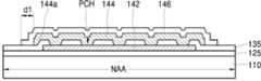
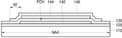
제2 패드(144)는 복수의 패드 컨택홀(PCH)을 통해 제1 패드(142)에 접속된다. 이러한 제2 패드(144)는 양측 장변으로부터 돌출된 복수의 돌출부(144a)를 갖는다. 이때, 복수의 돌출부(144a)는 복수의 패드 컨택홀(PCH)과 대응되는 동일 선상에 배치된다.
The
패드 전극(146)은 제2 패드(144) 상에 적층되어 제2 패드(144)에 접속된다. 이러한 패드 전극(146)은 제2 패드(144)의 외측으로 연장 배치된다. 이러한 패드 전극(146)은 제1 기판(110)의 표시 영역(AA)에 배치되는 유기발광 다이오드(E)의 제1 전극(160)과 동일층에 배치될 수 있다. 이에 따라, 패드 전극(146)은 ITO, IZO, ITZO 등의 투명한 금속 재질로 형성될 수 있다.The
전술한 제1 패드(142), 제2 패드(144) 및 패드 전극(146)을 포함하여 패드부(140)라 정의할 수 있다. 이때, 패드부(140)는 게이트 패드부 및 데이터 패드부를 포함할 수 있다. 이에 더불어, 패드부(140)는 복수의 데이터 배선과 이격 배치되는 전원공급 배선(미도시)과 연결되는 전원공급 패드부를 포함할 수 있다.
The above-described
외부 보호층(185)은 캡핑층(165) 및 패드 전극(146)을 덮으며, 패드 전극(146)의 일부를 노출시키는 패드 전극 컨택 홀(LCH)을 갖는다. 이러한 외부 보호층(185)의 재질로는, 일 예로 SiON가 이용될 수 있다. 이때, 패드 전극 컨택 홀(LCH)은 레이저 패터닝 장비를 이용한 레이저 패터닝 공정에 의해 패드 전극(146)의 일부를 덮는 외부 보호층(185)을 선택적으로 제거하는 것에 의해 형성된다.
The external
또한, 본 발명의 실시예에 따른 표시 장치(100)는 제2 기판(195) 및 보호 접착층(190)을 더 포함할 수 있다.Also, the
이때, 제2 기판(195)은 외부 보호층(185)과 이격된 상부에 배치된다. 제2 기판(195)의 재질로는 유리, 플라스틱, 스테인리스 스틸(stainless steel), 페이스 씰 메탈(face seal metal) 등이 이용될 수 있으며, 이 중 페이스 씰 메탈에 대한 사용이 증가하고 있다.At this time, the
또한, 보호 접착층(190)은 제2 기판(195)과 외부 보호층(185) 사이에 배치되어, 제1 및 제2 기판(110, 195)을 합착시키는 역할을 한다.
In addition, the protective
전술한 본 발명의 실시예에 따른 표시 장치(100)는 제2 패드(144)의 양측 장변에 돌출부(144a)를 설계하여 패드 전극(146)의 양측 장변 끝단으로부터 제2 패드의 돌출부(144a) 양측 장변 끝단까지의 간격과 패드 전극(146)의 양측 장변 끝단으로부터 제2 패드(144)의 비돌출부 양측 장변 끝단까지의 간격을 차등 설계하는 것을 통해 레이저 패터닝 공정시 잔막이 발생하는 불량을 개선하였다.
In the
이에 대해서는 이하 첨부된 도면을 참조하여 보다 구체적으로 설명하도록 한다.This will be described in more detail with reference to the accompanying drawings.
도 8은 도 7의 단위 패드부를 확대하여 나타낸 평면도이고, 도 9는 도 8의 Ⅸ-Ⅸ' 선을 따라 절단하여 나타낸 단면도이며, 도 10은 도 8의 Ⅹ-Ⅹ' 선을 따라 절단하여 나타낸 단면도이다.8 is an enlarged plan view of the unit pad part of FIG. 7, FIG. 9 is a cross-sectional view taken along line IX-IX' in FIG. 8, and FIG. 10 is taken along line X-X' in FIG. it is a cross section
도 8 내지 도 10에 도시된 바와 같이, 본 발명의 실시예에 따른 패드부 전극 구조(140)는 제1 패드(142), 절연막(125, 135), 제2 패드(144) 및 패드 전극(146)을 포함한다.
8 to 10, the pad
제1 패드(142)는 표시 영역(AA) 및 비표시 영역(NAA)을 갖는 제1 기판(110) 상의 비표시 영역(NAA)에 배치된다. 이러한 제1 패드(142)는 제1 기판(110) 상의 비표시 영역(NAA) 가장자리에 배치될 수 있다.
The
절연막(125, 135)은 제1 기판(110) 상의 표시 영역(AA) 및 비표시 영역(NAA)을 덮는다. 이러한 절연막(125, 135)은 제1 기판(110) 상에 차례로 적층된 제1 절연막(125) 및 제2 절연막(135)을 포함할 수 있다. 또한, 절연막(125, 135)은 제2 절연막(135) 상에 적층된 제3 절연막(도 6의 150)을 더 포함할 수도 있다. 이 중, 제2 절연막(135)은 제1 패드(142)의 일부를 노출시키는 복수의 패드 컨택홀(PCH)을 갖는다.The insulating
이때, 제1 절연막(125)은 게이트 절연막이고, 제2 절연막(135)은 층간 절연막이며, 제3 절연막은 보호막일 수 있다. 제3 절연막은 제1 기판(110) 상의 비표시 영역(NAA)에는 형성되지 않고, 표시 영역(AA)만을 덮도록 형성될 수도 있다.In this case, the first insulating
복수의 패드 컨택홀(PCH)은 제1 패드(142)를 덮는 제2 절연막(135)의 일부를 제거하는 것에 의해 형성될 수 있다. 이러한 복수의 패드 컨택홀(PCH)은 복수의 열 및 복수의 행을 갖는 매트릭스 형태로 이격 배치된다. 이때, 도 7에서는 복수의 패드 컨택홀(PCH)이 4 x 5 배열 구조를 일 예로 나타내었으나, 이는 예시적인 것으로 그 배열 구조는 다양한 형태가 적용될 수 있다.
The plurality of pad contact holes PCH may be formed by removing a portion of the second insulating
제2 패드(144)는 복수의 패드 컨택홀(PCH)을 통해 제1 패드(142)에 접속되며, 양측 장변으로부터 돌출된 복수의 돌출부(144a)를 갖는다. 이에 따라, 복수의 돌출부(144a)는 마주보는 양측에서 상호 대칭 구조로 돌출될 수 있다.The
이러한 돌출부(144a)의 형상은 사각형 형상을 가질 수 있으나, 이에 제한되는 것은 아니며, 삼각형, 오각형 등 다양한 형태로 설계 변경될 수도 있다.The shape of the
이때, 복수의 돌출부(144a)가 복수의 패드 컨택홀(PCH)과 동일 선상에 배치되지 않을 경우, 복수의 돌출부 형성 과정에서 미스 얼라인이 발생할 시 복수의 패드 컨택홀(PCH) 중 최외곽에 배치되는 패드 컨택홀(PCH)이 제2 패드(144)의 외측으로 벗어난 위치에 형성되는 컨택 불량이 발생될 수 있다. 따라서, 복수의 돌출부(144a)는 복수의 패드 컨택홀(PCH)과 동일 선상에 배치하는 것이 바람직하다.
At this time, when the plurality of
패드 전극(146)은 제2 패드(144) 상에 적층되어 제2 패드(144)에 접속되며, 제2 패드(144)의 외측으로 연장 배치된다. 이때, 패드 전극(146)은 제2 패드(144)와 중첩된 상부에서 제2 패드(144)의 외측으로 연장 배치된다. 이에 따라, 패드 전극(146)은 제2 패드(144)의 전체 면적을 덮는다.The
전술한 제1 패드(142)는 제1 절연막(125)과 제2 절연막(135) 사이에 배치되고, 제2 패드(144)는 제2 절연막(135) 상에 배치된다. 이때, 제1 패드(142)는 제1 기판(110) 상의 표시 영역(AA)에 배치되는 게이트 배선(미도시)과 동일층에서 동일한 물질을 이용하여 형성될 수 있다. 그리고, 제2 패드(144)는 제1 기판(110) 상의 표시 영역(AA)에 배치되는 데이터 배선(미도시)과 동일층에서 동일한 물질을 이용하여 형성될 수 있다.The aforementioned
이때, 제2 패드(144)는, 평면 상으로 볼 때, 양측 장변으로부터 돌출되는 돌출부(144a)를 가지며, 제1 면적을 갖는 직사각형으로 설계된다. 그리고, 패드 전극(146)은, 평면 상으로 볼 때, 제2 패드(144)와 중첩된 상부에서 제2 패드(144)의 외측으로 연장되어 제2 패드(144)를 감싸는 형태로 설계된다. 이에 따라, 패드 전극(146)은 제1 면적보다 넓은 제2 면적을 갖는다.At this time, when viewed in plan, the
특히, 패드 전극(146)의 양측 장변 끝단으로부터 제2 패드의 돌출부(144a) 양측 장변 끝단까지의 간격인 제1 간격(d1)은 각각 2.6 ~ 3.4㎛를 갖는다. 이와 달리, 패드 전극(146)의 양측 장변 끝단으로부터 제2 패드(144)의 비돌출부 양측 장변 끝단까지의 간격인 제2 간격(d2)은 각각 4 ~ 6㎛를 갖는다.In particular, the first distance d1, which is the distance from the ends of both long sides of the
또한, 인접한 패드 전극(146)들 사이의 간격(D)은 13.5 ~ 15.5㎛로 설계함으로써, 패드 전극(146)들 간의 이격 간격을 확보하였다.
In addition, the spacing D between the
이와 같이, 본 발명의 실시예에 따른 패드부 전극 구조(140)는 제2 패드(144)의 설계시 제2 패드(144)의 양측 장변으로부터 외측으로 돌출되는 돌출부(144a)를 설계함으로써, 제1 간격(d1)과 제2 간격(d2) 상호 간에 길이 편차를 갖도록 하였다.In this way, the pad
이에 따라, 본 발명의 실시예에 따른 패드부 전극 구조(140)는 패드 전극(146)의 면적 증가를 최소화면서도 돌출부(144a)의 설계를 통해 제2 패드(144)의 면적을 증가시킬 수 있으므로, 제2 패드(144)와 패드 전극(146) 간의 접촉 면적이 확장되는 효과로 본딩 저항성이 개선될 수 있다.Accordingly, the pad
따라서, 본 발명의 실시예에 따른 패드부 전극 구조(140)는 패드 전극(146)의 면적 증가를 최소화하면서도 돌출부(144a)를 갖는 제2 패드(144)를 통해, 레이저 패터닝 장비를 이용한 레이저 패터닝 공정시, 패드 전극(146) 및 제2 패드(144)의 접촉 면적 증가에 의한 전도도 증가로 열 전달이 효율적으로 이루어질 수 있으므로 패드 전극(146)을 덮는 외부 보호층(도 6의 185)을 완벽하게 제거하는 것이 가능하여, SiON 잔막 불량이 발생하지 않게 된다.
Therefore, the pad
이에 대해서는, 도 6 및 도 7을 다시 참조하여 보다 구체적으로 설명하도록 한다.This will be described in more detail with reference to FIGS. 6 and 7 again.
도 6 및 도 7에 도시된 바와 같이, 외부 보호층(185)은 마스크를 사용하는 것이 없이 제1 기판(110)의 전면에 증착하여 형성한 후, 레이저 패터닝 장비를 이용하여 패드 전극(146)을 덮는 외부 보호층(185)만을 선택적으로 제거하는 방식으로 패드 단자 컨택홀(LCH)을 형성하고 있다.As shown in FIGS. 6 and 7 , the outer
즉, 제1 기판(110) 상의 표시 영역(AA) 및 비표시 영역(NAA)의 전면에 마스크를 사용하는 것 없이 전면 증착을 통해 외부 보호층(185)을 형성한 후, 보호 접착층(190)을 매개로 제1 기판(110)과 제2 기판(195)을 합착시키게 된다.That is, after forming the external
이와 같이, 제1 기판(110) 및 제2 기판(195) 간의 합착이 완료되면, 패드 전극(146)을 덮는 외부 보호층(185)과 이격된 상부에 레이저 패터닝 장비를 장착시킨 상태에서 X축 및 Y축 방향을 따라 레이저 패터닝 장비를 이동해 가면서 레이저 조사를 실시하는 방식으로 제1 기판(110) 상의 패드 전극(146)을 노출시켜 패드 전극 컨택홀(LCH)을 형성하게 된다.
In this way, when the bonding between the
이때, 본 발명의 실시예에 따른 표시 장치(100)의 경우, 제1 간격(d1)은 2.6 ~ 3.4㎛를 갖도록 설계되고, 제2 간격(d2)은 4 ~ 6㎛를 갖도록 설계된다. 이 결과, 본 발명의 실시예에 따른 표시 장치(100)는 패드 전극(146)의 면적 증가를 최소화면서도 돌출부(144a)의 설계를 통해 제2 패드(144)의 면적을 증가시킬 수 있으므로, 제2 패드(144)와 패드 전극(146) 간의 접촉 면적이 확장되는 효과로 본딩 저항성을 개선할 수 있게 된다.In this case, in the case of the
이에 따라, 본 발명의 실시예에 따른 표시 장치(100)는 패드 전극(146)의 면적 증가를 최소화하면서도 돌출부(144a)를 갖는 제2 패드(144)를 통해, 레이저 패터닝 장비를 이용한 레이저 패터닝 공정시, 패드 전극(146) 및 제2 패드(144)의 접촉 면적 증가에 의한 전도도 증가로 열 전달이 효율적으로 이루어질 수 있다.Accordingly, in the
이 결과, 본 발명의 실시예에 따른 표시 장치(100)는 패드 전극(146)을 덮는 외부 보호층(185)을 완벽하게 제거하는 것이 가능하여, SiON 잔막 불량이 발생하지 않게 되므로 생산 수율을 향상시킬 수 있다.
As a result, in the
이상에서는 본 발명의 실시예를 중심으로 설명하였지만, 통상의 기술자의 수준에서 다양한 변경이나 변형을 가할 수 있다. 따라서, 이러한 변경과 변형이 본 발명의 범위를 벗어나지 않는 한 본 발명의 범주 내에 포함되는 것으로 이해할 수 있을 것이다.
Although the above has been described based on the embodiments of the present invention, various changes or modifications may be made at the level of those skilled in the art. Accordingly, it will be understood that such changes and modifications are included within the scope of the present invention as long as they do not depart from the scope of the present invention.
100 : 표시 장치110 : 제1 기판
120 : 반도체층122 : 게이트 전극
125 : 게이트 절연막132 : 소스 전극
134 : 드레인 전극135 : 층간 절연막
140 : 패드부142 : 제1 패드
144 : 제2 패드146 : 패드 전극
150 : 보호막155 : 뱅크층
160 : 제1 전극165 : 캡핑층
170 : 유기 발광층180 : 제2 전극
185 : 외부 보호층190 : 보호 접착층
195 : 제2 기판DTr : 박막 트랜지스터
E : 유기발광 다이오드DCH : 드레인 컨택홀
PCH : 패드 컨택홀LCH : 패드 전극 컨택홀
AA : 표시 영역NAA : 비표시 영역100: display device 110: first substrate
120: semiconductor layer 122: gate electrode
125: gate insulating film 132: source electrode
134: drain electrode 135: interlayer insulating film
140: pad part 142: first pad
144: second pad 146: pad electrode
150: protective film 155: bank layer
160: first electrode 165: capping layer
170: organic light emitting layer 180: second electrode
185: external protective layer 190: protective adhesive layer
195: second substrate DTr: thin film transistor
E: organic light emitting diode DCH: drain contact hole
PCH: Pad contact hole LCH: Pad electrode contact hole
AA: display area NAA: non-display area
Claims (10)
Translated fromKorean상기 기판 상의 표시 영역 및 비표시 영역을 덮으며, 상기 제1 패드의 일부를 노출시키는 복수의 패드 컨택홀을 갖는 절연막;
상기 복수의 패드 컨택홀을 통해 상기 제1 패드에 접속되며, 양측 장변으로부터 돌출된 복수의 돌출부를 갖는 제2 패드; 및
상기 제2 패드 상에 적층되어 상기 제2 패드에 접속되며, 상기 제2 패드의 외측으로 연장 배치된 패드 전극;
을 포함하고,
상기 복수의 패드 컨택홀은
복수의 열 및 복수의 행을 갖는 매트릭스 형태로 이격 배치된 패드부 전극 구조.
a first pad disposed in the non-display area on a substrate having a display area and a non-display area;
an insulating layer covering a display area and a non-display area on the substrate and having a plurality of pad contact holes exposing a portion of the first pad;
a second pad connected to the first pad through the plurality of pad contact holes and having a plurality of protrusions protruding from both long sides; and
a pad electrode stacked on the second pad, connected to the second pad, and extending outwardly of the second pad;
including,
The plurality of pad contact holes are
A pad part electrode structure spaced apart in a matrix form having a plurality of columns and a plurality of rows.
상기 패드 전극은
상기 제2 패드와 중첩된 상부에서 상기 제2 패드의 외측으로 연장 배치되어, 상기 제2 패드의 전체 면적을 덮는 패드부 전극 구조.
According to claim 1,
The pad electrode is
A pad portion electrode structure extending outwardly of the second pad from an upper portion overlapping the second pad and covering the entire area of the second pad.
상기 복수의 돌출부는
상기 복수의 패드 컨택홀과 동일 선상에 배치된 패드부 전극 구조.
According to claim 1,
The plurality of protrusions
A pad portion electrode structure disposed on the same line as the plurality of pad contact holes.
상기 패드 전극의 양측 장변 끝단으로부터 상기 제2 패드의 돌출부 양측 장변 끝단까지의 간격은 2.6 ~ 3.4㎛를 갖는 패드부 전극 구조.
According to claim 1,
A pad part electrode structure having a distance from both long side ends of the pad electrode to both long side ends of the protrusion of the second pad in a range of 2.6 to 3.4 μm.
상기 패드 전극의 양측 장변 끝단으로부터 상기 제2 패드의 비돌출부 양측 장변 끝단까지의 간격은 4 ~ 6㎛를 갖는 패드부 전극 구조.
According to claim 1,
A pad part electrode structure having a distance from both long side ends of the pad electrode to both long side ends of the non-protruding portion of the second pad of 4 to 6 μm.
상기 절연막은
상기 기판 상의 비표시 영역에 배치된 게이트 절연막과,
상기 게이트 절연막 상에 배치되는 층간 절연막을 포함하는 패드부 전극 구조.
According to claim 1,
the insulating film
a gate insulating layer disposed in a non-display area on the substrate;
A pad portion electrode structure including an interlayer insulating film disposed on the gate insulating film.
상기 제1 패드는
상기 게이트 절연막과 층간 절연막 사이에 배치되고, 상기 제2 패드는 상기 층간 절연막 상에 배치된 패드부 전극 구조.
According to claim 7,
The first pad
A pad portion electrode structure disposed between the gate insulating film and the interlayer insulating film, and wherein the second pad is disposed on the interlayer insulating film.
상기 제1 기판 상의 표시 영역에 배치된 박막 트랜지스터;
상기 박막 트랜지스터에 연결된 유기발광 다이오드;
상기 유기발광 다이오드를 덮는 캡핑층;
상기 제1 기판 상의 비표시 영역에 배치된 제1 패드;
상기 제1 기판 상의 표시 영역 및 비표시 영역을 덮으며, 상기 제1 패드의 일부를 노출시키는 복수의 패드 컨택홀을 갖는 절연막;
상기 복수의 패드 컨택홀을 통해 상기 제1 패드에 접속되며, 양측 장변으로부터 돌출된 복수의 돌출부를 갖는 제2 패드;
상기 제2 패드 상에 적층되어 상기 제2 패드에 접속되며, 상기 제2 패드의 외측으로 연장 배치된 패드 전극; 및
상기 캡핑층 및 패드 전극을 덮으며, 상기 패드 전극의 일부를 노출시키는 패드 전극 컨택 홀을 갖는 외부 보호층;
을 포함하고,
상기 복수의 패드 컨택홀은
복수의 열 및 복수의 행을 갖는 매트릭스 형태로 이격 배치된 표시 장치.
a first substrate having a display area and a non-display area;
a thin film transistor disposed in a display area on the first substrate;
an organic light emitting diode connected to the thin film transistor;
a capping layer covering the organic light emitting diode;
a first pad disposed in a non-display area on the first substrate;
an insulating layer covering a display area and a non-display area on the first substrate and having a plurality of pad contact holes exposing a portion of the first pad;
a second pad connected to the first pad through the plurality of pad contact holes and having a plurality of protrusions protruding from both long sides;
a pad electrode stacked on the second pad, connected to the second pad, and extending outwardly of the second pad; and
an external protective layer covering the capping layer and the pad electrode and having a pad electrode contact hole exposing a portion of the pad electrode;
including,
The plurality of pad contact holes are
A display device spaced apart from each other in a matrix form having a plurality of columns and a plurality of rows.
상기 외부 보호층과 이격된 상부에 배치된 제2 기판과,
상기 제2 기판과 외부 보호층 사이에 배치되어, 상기 제1 및 제2 기판을 합착시키는 보호 접착층을 더 포함하는 표시 장치.According to claim 9,
A second substrate disposed on an upper portion spaced apart from the outer protective layer;
and a protective adhesive layer disposed between the second substrate and the external protective layer to bond the first and second substrates together.
Priority Applications (1)
| Application Number | Priority Date | Filing Date | Title |
|---|---|---|---|
| KR1020150191773AKR102468198B1 (en) | 2015-12-31 | 2015-12-31 | Pad area electrode structure and display device having the same |
Applications Claiming Priority (1)
| Application Number | Priority Date | Filing Date | Title |
|---|---|---|---|
| KR1020150191773AKR102468198B1 (en) | 2015-12-31 | 2015-12-31 | Pad area electrode structure and display device having the same |
Publications (2)
| Publication Number | Publication Date |
|---|---|
| KR20170081052A KR20170081052A (en) | 2017-07-11 |
| KR102468198B1true KR102468198B1 (en) | 2022-11-17 |
Family
ID=59354856
Family Applications (1)
| Application Number | Title | Priority Date | Filing Date |
|---|---|---|---|
| KR1020150191773AActiveKR102468198B1 (en) | 2015-12-31 | 2015-12-31 | Pad area electrode structure and display device having the same |
Country Status (1)
| Country | Link |
|---|---|
| KR (1) | KR102468198B1 (en) |
Families Citing this family (4)
| Publication number | Priority date | Publication date | Assignee | Title |
|---|---|---|---|---|
| KR102674308B1 (en)* | 2018-10-05 | 2024-06-10 | 엘지디스플레이 주식회사 | Display Device |
| KR102776430B1 (en)* | 2019-02-21 | 2025-03-05 | 삼성디스플레이 주식회사 | Dispcay device |
| KR102843099B1 (en)* | 2019-07-12 | 2025-08-06 | 삼성디스플레이 주식회사 | Display device and method of manufacturing for display device |
| KR20220153155A (en) | 2021-05-10 | 2022-11-18 | 삼성디스플레이 주식회사 | Display device |
Family Cites Families (2)
| Publication number | Priority date | Publication date | Assignee | Title |
|---|---|---|---|---|
| KR102033615B1 (en)* | 2013-09-27 | 2019-10-17 | 엘지디스플레이 주식회사 | Organic light emitting display device and method for manufacturing of the same |
| KR102119087B1 (en)* | 2014-02-17 | 2020-06-04 | 엘지디스플레이 주식회사 | Organic light emitting display device |
- 2015
- 2015-12-31KRKR1020150191773Apatent/KR102468198B1/enactiveActive
Also Published As
| Publication number | Publication date |
|---|---|
| KR20170081052A (en) | 2017-07-11 |
Similar Documents
| Publication | Publication Date | Title |
|---|---|---|
| JP6756508B2 (en) | Display device | |
| US10957744B2 (en) | Display device including process key | |
| JP5161263B2 (en) | Flat panel display device and manufacturing method thereof | |
| CN104425550B (en) | Flexible organic electro-luminescence device and its manufacturing method | |
| US20170082888A1 (en) | Display device | |
| US8519616B2 (en) | Organic electroluminescent display device and method of fabricating the same | |
| JP2018049774A (en) | Display device | |
| CN103681742A (en) | Organic light emitting display and manufacturing method thereof | |
| CN103811501A (en) | Flexible display device | |
| TW201413930A (en) | Organic light emitting display device | |
| KR20110047654A (en) | Manufacturing method of organic light emitting device | |
| KR102100656B1 (en) | Organic light emitting display device and method of fabricating thereof | |
| KR102468198B1 (en) | Pad area electrode structure and display device having the same | |
| CN100461444C (en) | Light emitting display and manufacturing method thereof | |
| KR102337806B1 (en) | Organic light emitting diode display | |
| JP6719948B2 (en) | Display device | |
| CN103681694A (en) | Flexible display substrate and flexible display device | |
| CN102097453A (en) | Organic electroluminescent display device | |
| KR102544942B1 (en) | Display Device And Method Of Fabricating The Same | |
| KR101311670B1 (en) | Organic Electroluminescent Device and method for fabricating thereof | |
| CN107797344A (en) | Array base palte, display panel and its manufacture method | |
| CN101908554B (en) | Organic electroluminescence display device and manufacturing method thereof | |
| KR102087193B1 (en) | Method for manufacturing organic light emitting diode display and method for manufacturing touch panel | |
| KR20150070544A (en) | Organic Light Emitting Display Device and Method of manufacturing the same | |
| KR101251375B1 (en) | Dual panel type organic electro-luminescent device |
Legal Events
| Date | Code | Title | Description |
|---|---|---|---|
| PA0109 | Patent application | Patent event code:PA01091R01D Comment text:Patent Application Patent event date:20151231 | |
| PG1501 | Laying open of application | ||
| A201 | Request for examination | ||
| PA0201 | Request for examination | Patent event code:PA02012R01D Patent event date:20201217 Comment text:Request for Examination of Application Patent event code:PA02011R01I Patent event date:20151231 Comment text:Patent Application | |
| E902 | Notification of reason for refusal | ||
| PE0902 | Notice of grounds for rejection | Comment text:Notification of reason for refusal Patent event date:20220203 Patent event code:PE09021S01D | |
| E701 | Decision to grant or registration of patent right | ||
| PE0701 | Decision of registration | Patent event code:PE07011S01D Comment text:Decision to Grant Registration Patent event date:20220816 | |
| GRNT | Written decision to grant | ||
| PR0701 | Registration of establishment | Comment text:Registration of Establishment Patent event date:20221114 Patent event code:PR07011E01D | |
| PR1002 | Payment of registration fee | Payment date:20221114 End annual number:3 Start annual number:1 | |
| PG1601 | Publication of registration |