KR102467253B1 - Bridgeless type switching rectifier - Google Patents
Bridgeless type switching rectifierDownload PDFInfo
- Publication number
- KR102467253B1 KR102467253B1KR1020200186177AKR20200186177AKR102467253B1KR 102467253 B1KR102467253 B1KR 102467253B1KR 1020200186177 AKR1020200186177 AKR 1020200186177AKR 20200186177 AKR20200186177 AKR 20200186177AKR 102467253 B1KR102467253 B1KR 102467253B1
- Authority
- KR
- South Korea
- Prior art keywords
- low
- speed switch
- speed
- switch
- inductor
- Prior art date
- Legal status (The legal status is an assumption and is not a legal conclusion. Google has not performed a legal analysis and makes no representation as to the accuracy of the status listed.)
- Active
Links
- 239000003990capacitorSubstances0.000claimsdescription11
- 230000003071parasitic effectEffects0.000claimsdescription6
- 230000000694effectsEffects0.000description5
- 238000006243chemical reactionMethods0.000description4
- 238000010586diagramMethods0.000description4
- 238000000034methodMethods0.000description4
- 238000012986modificationMethods0.000description3
- 230000004048modificationEffects0.000description3
- 238000007599dischargingMethods0.000description2
- 230000014509gene expressionEffects0.000description2
- 239000004065semiconductorSubstances0.000description2
- 238000009499grossingMethods0.000description1
- 230000017525heat dissipationEffects0.000description1
Images


Classifications
- H—ELECTRICITY
- H02—GENERATION; CONVERSION OR DISTRIBUTION OF ELECTRIC POWER
- H02M—APPARATUS FOR CONVERSION BETWEEN AC AND AC, BETWEEN AC AND DC, OR BETWEEN DC AND DC, AND FOR USE WITH MAINS OR SIMILAR POWER SUPPLY SYSTEMS; CONVERSION OF DC OR AC INPUT POWER INTO SURGE OUTPUT POWER; CONTROL OR REGULATION THEREOF
- H02M1/00—Details of apparatus for conversion
- H02M1/42—Circuits or arrangements for compensating for or adjusting power factor in converters or inverters
- H02M1/4208—Arrangements for improving power factor of AC input
- H02M1/4225—Arrangements for improving power factor of AC input using a non-isolated boost converter
- H—ELECTRICITY
- H02—GENERATION; CONVERSION OR DISTRIBUTION OF ELECTRIC POWER
- H02M—APPARATUS FOR CONVERSION BETWEEN AC AND AC, BETWEEN AC AND DC, OR BETWEEN DC AND DC, AND FOR USE WITH MAINS OR SIMILAR POWER SUPPLY SYSTEMS; CONVERSION OF DC OR AC INPUT POWER INTO SURGE OUTPUT POWER; CONTROL OR REGULATION THEREOF
- H02M1/00—Details of apparatus for conversion
- H02M1/0048—Circuits or arrangements for reducing losses
- H02M1/0054—Transistor switching losses
- H—ELECTRICITY
- H02—GENERATION; CONVERSION OR DISTRIBUTION OF ELECTRIC POWER
- H02M—APPARATUS FOR CONVERSION BETWEEN AC AND AC, BETWEEN AC AND DC, OR BETWEEN DC AND DC, AND FOR USE WITH MAINS OR SIMILAR POWER SUPPLY SYSTEMS; CONVERSION OF DC OR AC INPUT POWER INTO SURGE OUTPUT POWER; CONTROL OR REGULATION THEREOF
- H02M7/00—Conversion of AC power input into DC power output; Conversion of DC power input into AC power output
- H02M7/02—Conversion of AC power input into DC power output without possibility of reversal
- H02M7/04—Conversion of AC power input into DC power output without possibility of reversal by static converters
- H02M7/12—Conversion of AC power input into DC power output without possibility of reversal by static converters using discharge tubes with control electrode or semiconductor devices with control electrode
- H02M7/21—Conversion of AC power input into DC power output without possibility of reversal by static converters using discharge tubes with control electrode or semiconductor devices with control electrode using devices of a triode or transistor type requiring continuous application of a control signal
- H02M7/217—Conversion of AC power input into DC power output without possibility of reversal by static converters using discharge tubes with control electrode or semiconductor devices with control electrode using devices of a triode or transistor type requiring continuous application of a control signal using semiconductor devices only
- Y—GENERAL TAGGING OF NEW TECHNOLOGICAL DEVELOPMENTS; GENERAL TAGGING OF CROSS-SECTIONAL TECHNOLOGIES SPANNING OVER SEVERAL SECTIONS OF THE IPC; TECHNICAL SUBJECTS COVERED BY FORMER USPC CROSS-REFERENCE ART COLLECTIONS [XRACs] AND DIGESTS
- Y02—TECHNOLOGIES OR APPLICATIONS FOR MITIGATION OR ADAPTATION AGAINST CLIMATE CHANGE
- Y02B—CLIMATE CHANGE MITIGATION TECHNOLOGIES RELATED TO BUILDINGS, e.g. HOUSING, HOUSE APPLIANCES OR RELATED END-USER APPLICATIONS
- Y02B70/00—Technologies for an efficient end-user side electric power management and consumption
- Y02B70/10—Technologies improving the efficiency by using switched-mode power supplies [SMPS], i.e. efficient power electronics conversion e.g. power factor correction or reduction of losses in power supplies or efficient standby modes
- Y—GENERAL TAGGING OF NEW TECHNOLOGICAL DEVELOPMENTS; GENERAL TAGGING OF CROSS-SECTIONAL TECHNOLOGIES SPANNING OVER SEVERAL SECTIONS OF THE IPC; TECHNICAL SUBJECTS COVERED BY FORMER USPC CROSS-REFERENCE ART COLLECTIONS [XRACs] AND DIGESTS
- Y02—TECHNOLOGIES OR APPLICATIONS FOR MITIGATION OR ADAPTATION AGAINST CLIMATE CHANGE
- Y02T—CLIMATE CHANGE MITIGATION TECHNOLOGIES RELATED TO TRANSPORTATION
- Y02T10/00—Road transport of goods or passengers
- Y02T10/60—Other road transportation technologies with climate change mitigation effect
- Y02T10/72—Electric energy management in electromobility
Landscapes
- Engineering & Computer Science (AREA)
- Power Engineering (AREA)
- Rectifiers (AREA)
Abstract
Translated fromKoreanDescription
Translated fromKorean본 발명은 브릿지리스형 스위칭 정류기에 관한 것으로서, 더욱 상세하게는, 제1 및 제2 고속 스위치와, 제1 및 제2 저속 스위치의 스위칭 동작 시 동작 손실을 저감시킬 수 있는 브릿지리스형 스위칭 정류기에 관한 것이다.The present invention relates to a bridgeless switching rectifier, and more particularly, to a bridgeless switching rectifier capable of reducing operating loss during a switching operation of first and second high-speed switches and first and second low-speed switches. it's about
일반적으로 스위칭 전원장치는 안정된 출력전압을 목적으로 하는 전력변환 장치이다. 특히, 교류를 입력으로 하는 스위칭 전원장치의 경우, 교류전압을 직류전압으로 변환시키는 정류회로가 필수적으로 이용되는데 이 때 주로 사용되는 회로방식이 부스트 컨버터이다. 부스트 컨버터는 입력전압보다 높은 출력전압으로 변환하는 경우 사용되는 회로방식이지만 입력단에 인덕터가 있어서 입력전류가 연속적으로 흐르기 때문에 입력단 필터의 부담이 작고 간단한 전류 필터 구성이 가능하다는 장점이 있다.In general, a switching power supply is a power conversion device aimed at a stable output voltage. In particular, in the case of a switching power supply having an alternating current as an input, a rectifier circuit that converts an alternating current voltage into a direct current voltage is essentially used, and a circuit method mainly used in this case is a boost converter. The boost converter is a circuit method used when converting an output voltage higher than the input voltage, but has the advantage of being able to configure a simple current filter with a small burden on the input filter because there is an inductor at the input so that the input current flows continuously.
부스트 컨버터를 기본으로 하는 정류회로(이하, '스위칭 정류기')는 기본적으로 교류전압을 직류전압으로 변환시키는 기능 외에도 입력전류의 파형을 입력전압 파형과 같아지도록 제어하여 입력 역률을 높이고 고조파를 저감시키는 부가적인 기능을 수행하게 된다. 또한, 고주파 스위칭 동작 때문에 주요 소자의 사이즈를 줄일 수 있고 내부 손실이 저감되므로 전력변환 효율을 높일 수 있는 정류방식으로 널리 알려져 있다.A rectifier circuit based on a boost converter (hereinafter referred to as 'switching rectifier') basically controls the waveform of the input current to be the same as the waveform of the input voltage in addition to the function of converting AC voltage to DC voltage to increase the input power factor and reduce harmonics. perform additional functions. In addition, it is widely known as a rectification method capable of increasing power conversion efficiency because the size of main elements can be reduced due to high-frequency switching operation and internal loss is reduced.
도 1은 일반적인 브릿지리스형 스위칭 정류기를 나타낸 회로도이다.1 is a circuit diagram showing a general bridgeless switching rectifier.
도 1에 나타낸 브릿지리스형 스위칭 정류기는, 한 개 이상의 반도체 스위치를 사용하여 교류전압을 직류전압으로 정류할 시, 입력전류를 입력전압과 같은 위상을 유지하면서 정현파를 생성시키는 역할을 수행하게 된다.The bridgeless switching rectifier shown in FIG. 1 serves to generate a sine wave while maintaining the same phase as the input current when an AC voltage is rectified into a DC voltage using one or more semiconductor switches.
먼저, 브릿지형 스위칭 정류기는 큰 출력을 필요로 하는 전기자동차의 충전기나 모터의 구동 시, 브릿지 다이오드를 지나는 전류의 양이 증가함에 따라 브릿지 다이오드에서 발생하는 열로 인해 전도손실이 증가하여 전체적인 효율이 떨어지는 문제점이 있었다.First, in the bridge-type switching rectifier, conduction loss increases due to heat generated in the bridge diode as the amount of current passing through the bridge diode increases when driving an electric vehicle charger or motor that requires a large output, resulting in a decrease in overall efficiency. There was a problem.
이에 따라, 브릿지 다이오드를 사용하지 않는 브릿지리스형 스위칭 정류기가 제안되었다.Accordingly, a bridgeless switching rectifier that does not use a bridge diode has been proposed.
브릿지리스형 스위칭 정류기는 입력단에 브릿지 다이오드를 사용하지 않고 정류기 동작을 수행하기 때문에 정류기의 전도손실이 저감되어 전력변환 효율이 증가하고, 내부손실이 저감되는 회로방식으로서 브릿지형 스위칭 정류기를 대체하여 널리 사용되어 왔다.A bridgeless switching rectifier is a circuit method in which the conduction loss of the rectifier is reduced, the power conversion efficiency is increased, and the internal loss is reduced because the rectifier operation is performed without using a bridge diode at the input stage. has been used
그러나 이러한 브릿지리스형 스위칭 정류기는 출력 전력용량이 증가할수록 다이오드 및 스위치, 예를 들어 MOSFET와 같은 반도체 스위치의 정격이 증가하는 동시에 전력손실이 발생된다.However, in such a bridgeless switching rectifier, as the output power capacity increases, ratings of diodes and switches, for example, semiconductor switches such as MOSFETs, increase, and at the same time, power loss occurs.
그 결과, 전통적인 브릿지리스형 스위칭 정류기는 전력 손실이 증가하여 전력변환 효율이 낮아지는 문제가 존재한다. 이러한 소자의 전력손실은 고도한 방열기구의 사용을 필요로 하기 때문에 정류기의 전체적인 크기가 증가하여 전력밀도에 영향을 주게 된다. 또한, 브릿지리스형 스위칭 정류기는 회로구조상 두 개 이상의 인덕터를 사용해야 하므로, 인덕터에 의하여 크기가 더욱 커지고, 무거우며, 비싸다는 단점을 갖는다.As a result, the traditional bridgeless switching rectifier has a problem in that power loss is increased and power conversion efficiency is lowered. Since the power loss of these devices requires the use of a high heat dissipation mechanism, the overall size of the rectifier increases, which affects the power density. In addition, since the bridgeless switching rectifier requires the use of two or more inductors in terms of its circuit structure, the inductor makes the rectifier larger in size, heavier, and more expensive.
본 발명의 목적은, 제1 및 제2 고속 스위치와, 제1 및 제2 저속 스위치의 스위칭 동작 시 동작 손실을 저감시킬 수 있는 브릿지리스형 스위칭 정류기를 제공함에 있다.An object of the present invention is to provide a bridgeless switching rectifier capable of reducing operating loss during a switching operation of first and second high-speed switches and first and second low-speed switches.
본 발명의 목적들은 이상에서 언급한 목적으로 제한되지 않으며, 언급되지 않은 본 발명의 다른 목적 및 장점들은 하기의 설명에 의해서 이해될 수 있고, 본 발명의 실시예에 의해 보다 분명하게 이해될 것이다. 또한, 본 발명의 목적 및 장점들은 특허 청구 범위에 나타낸 수단 및 그 조합에 의해 실현될 수 있음을 쉽게 알 수 있을 것이다.The objects of the present invention are not limited to the above-mentioned objects, and other objects and advantages of the present invention not mentioned above can be understood by the following description and will be more clearly understood by the examples of the present invention. It will also be readily apparent that the objects and advantages of the present invention may be realized by means of the instrumentalities and combinations indicated in the claims.
본 발명에 따른 브릿지리스형 스위칭 정류기는, 인덕터, 서로 병렬 연결된 제1 및 제2 다이오드, 제1 노드에서, 상기 인덕터 및 상기 제1 다이오드와 연결된 제1 고속 스위치, 상기 제1 노드에서 상기 제1 고속 스위치와 연결된 제1 저속 스위치, 제2 노드에서 상기 제2 다이오드와 연결되며, 상기 제1 고속 스위치와 동일하게 턴온 및 턴오프 동작하는 제2 고속 스위치, 상기 제2 노드에서 상기 제2 다이오드 및 상기 제2 고속 스위치와 연결된 제2 저속 스위치 및 상기 제1 노드에 인가된 제1 전압 및 상기 제2 노드에 인가된 제2 전압에 따라 상기 제1 및 제2 저속 스위치 중 어느 하나를 턴온 동작시키는 스위치 구동회로를 포함할 수 있다.A bridgeless switching rectifier according to the present invention includes an inductor, first and second diodes connected in parallel to each other, a first high-speed switch connected to the inductor and the first diode at a first node, and the first diode at the first node. A first low-speed switch connected to a high-speed switch, a second high-speed switch connected to the second diode at a second node and turning on and off in the same manner as the first high-speed switch, the second diode at the second node, and Turning on any one of the first and second low-speed switches according to a second low-speed switch connected to the second high-speed switch and a first voltage applied to the first node and a second voltage applied to the second node A switch driving circuit may be included.
상기 제1 저속 스위치는, 입력 전원의 네거티브 주기에 턴온 동작하고, 상기 제2 저속 스위치는, 상기 입력 전원의 포지티브 주기에 턴온 동작할 수 있다.The first low-speed switch may turn on during a negative cycle of input power, and the second low-speed switch may turn on during a positive cycle of input power.
상기 스위치 구동회로는, 상기 제1 저속 스위치의 드레인과 상기 제2 저속 스위치의 소오스 사이에 연결된 제1 저항, 상기 제2 저속 스위치의 드레인과 상기 제1 저속 스위치의 소오스 사이에 연결된 제2 저항, 상기 제1 저속 스위치의 소오스와 상기 제2 저항 사이에 연결되어, 상기 제1 저속 스위치를 턴온 동작시키는 제1 스위치 구동부 및 상기 제2 저속 스위치의 소오스와 상기 제1 저항 사이에 연결되어, 상기 제2 저속 스위치를 턴온 동작시키는 제2 스위치 구동부를 포함할 수 있다.The switch driving circuit includes a first resistor connected between the drain of the first low-speed switch and the source of the second low-speed switch, a second resistor connected between the drain of the second low-speed switch and the source of the first low-speed switch, A first switch driver connected between the source of the first low-speed switch and the second resistor to turn on the first low-speed switch and connected between the source of the second low-speed switch and the first resistor, 2 may include a second switch driver for turning on the low speed switch.
상기 제1 스위치 구동부는, 상기 제2 저항과 연결되며, 상기 제2 전압을 분배하는 제1 분배 저항, 상기 제2 저항 및 상기 제1 분배 저항에 의해 분배된 제1 분배전압의 리플을 보상하는 제1 커패시터 및 상기 제1 분배 저항과 병렬 연결되며, 상기 제1 분배전압을 소정전압으로 유지하여 상기 제1 저속 스위치가 턴온 동작되게 상기 제1 저속 스위치의 소오스로 공급하는 제1 정전압 다이오드를 포함할 수 있다.The first switch driver is connected to the second resistor, and compensates for the ripple of the first distribution voltage divided by the first distribution resistor for distributing the second voltage and the second resistor and the first distribution resistor. A first constant voltage diode connected in parallel with a first capacitor and the first distribution resistor, maintaining the first distribution voltage at a predetermined voltage and supplying it to a source of the first low-speed switch to turn on the first low-speed switch. can do.
상기 제2 스위치 구동부는, 상기 제1 저항과 연결되며, 상기 제1 전압을 분배하는 제2 분배 저항, 상기 제1 저항 및 상기 제2 분배 저항에 의해 분배된 제2 분배전압의 리플을 보상하는 제2 커패시터 및 상기 제2 분배 저항과 병렬 연결되며, 상기 제2 분배전압을 소정전압으로 유지하여 상기 제2 저속 스위치가 턴온 동작되게 상기 제2 저속 스위치의 소오스로 공급하는 제2 정전압 다이오드를 포함할 수 있다.The second switch driving unit is connected to the first resistor and compensates for a second distribution resistor for distributing the first voltage and a ripple of a second distribution voltage divided by the first resistor and the second distribution resistor. A second constant voltage diode connected in parallel with a second capacitor and the second distribution resistor, maintaining the second distribution voltage at a predetermined voltage and supplying it to a source of the second low-speed switch to turn on the second low-speed switch. can do.
상기 인덕터에 AC 전원의 포지티브 전원이 공급되어, 상기 인덕터에 인덕터 전류가 충전되기 이전인 경우, 상기 제1, 2 고속 스위치는, 턴온 동작하고, 상기 제2 저속 스위치는, 상기 제2 스위치 구동부에서 공급되는 상기 제2 분배전압에 의해 턴온동작하여, 상기 제1, 2 고속 스위치와 제1 전류패스를 형성할 수 있다.When positive power of AC power is supplied to the inductor and before the inductor current is charged in the inductor, the first and second high-speed switches turn on, and the second low-speed switch operates in the second switch driving unit. A turn-on operation is performed by the supplied second divided voltage to form a first current path with the first and second high-speed switches.
상기 인턱터에 상기 인덕턴 전류가 충전된 경우, 상기 제1, 2 고속 스위치는, 턴오프 동작하고, 상기 제2 저속 스위치는, 턴온 동작을 유지하며, 상기 제1 다이오드, 출력 저항 및 상기 제2 고속 스위치의 기생 다이오드와 제2 전류 패스를 형성할 수 있다.When the inductor is charged with the inductance current, the first and second high-speed switches turn off, and the second low-speed switch maintains a turn-on operation, and the first diode, the output resistance and the second A second current path may be formed with the parasitic diode of the high-speed switch.
상기 인덕터에 AC 전원의 네거티브 전원이 공급되어, 상기 인덕터에 인덕터 전류가 충전되기 이전인 경우, 상기 제1, 2 고속 스위치는, 턴온 동작하고, 상기 제1 저속 스위치는, 상기 제1 스위치 구동부에서 공급되는 상기 제1 분배전압에 의해 턴온동작하여, 상기 제1, 2 고속 스위치와 제3 전류패스를 형성할 수 있다.When negative power of AC power is supplied to the inductor and before the inductor current is charged in the inductor, the first and second high-speed switches turn on, and the first low-speed switch operates in the first switch driving unit. A turn-on operation is performed by the supplied first divided voltage to form a third current path with the first and second high-speed switches.
상기 인턱터에 상기 인덕턴 전류가 충전된 경우, 상기 제1, 2 고속 스위치는, 턴오프 동작하고, 상기 제1 저속 스위치는, 턴온 동작을 유지하며, 상기 제2 다이오드, 출력 저항 및 상기 제1 고속 스위치의 기생 다이오드와 제4 전류 패스를 형성할 수 있다.When the inductor is charged with the inductance current, the first and second high-speed switches turn off, and the first low-speed switch maintains a turn-on operation, and the second diode, the output resistance and the first A fourth current path may be formed with the parasitic diode of the high-speed switch.
본 발명에 따른 브릿지리스형 스위칭 정류기는, 하나의 인덕터를 사용하며 제1 및 제2 고속 스위치와, 제1 및 제2 저속 스위치의 스위칭 동작 시 동작 손실을 저감시킬 수 있는 이점이 있다.The bridgeless switching rectifier according to the present invention uses one inductor and has an advantage of reducing operating loss during switching operations of the first and second high-speed switches and the first and second low-speed switches.
또한, 본 발명에 따른 브릿지리스형 스위칭 정류기는, 하나의 인덕터를 사용함으로써, 크기를 줄일 수 있으며 그에 따른 원가를 절감할 수 있는 이점이 있다.In addition, the bridgeless switching rectifier according to the present invention has the advantage of being able to reduce the size and reduce the cost by using one inductor.
또한, 본 발명에 따른 브릿지리스형 스위칭 정류기는, 제1 및 제2 저속 스위치를 이용하여 제1 및 제2 고속 스위치의 스위칭 손실을 줄일 수 있는 이점이 있다.In addition, the bridgeless switching rectifier according to the present invention has an advantage in that switching loss of the first and second high-speed switches can be reduced by using the first and second low-speed switches.
한편, 본 발명의 효과는 이상에서 언급한 효과들로 제한되지 않으며, 이하에서 설명할 내용으로부터 통상의 기술자에게 자명한 범위 내에서 다양한 효과들이 포함될 수 있다.On the other hand, the effects of the present invention are not limited to the effects mentioned above, and various effects may be included within a range apparent to those skilled in the art from the contents to be described below.
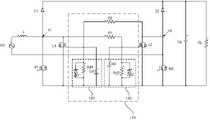
도 1은 일반적인 브릿지리스형 스위칭 정류기를 나타낸 회로도이다.
도 2는 본 발명에 따른 브릿지리스형 스위칭 정류기를 나타낸 회로도이다.
도 3 내지 도 5는 본 발명에 따른 브릿지리스형 스위칭 정류기로 포지티스 전원이 공급되는 경우의 전류패스를 나타낸다.
도 6 내지 도 8은 본 발명에 따른 브릿지리스형 스위칭 정류기로 네거티스 전원이 공급되는 경우의 전류패스를 나타낸다.1 is a circuit diagram showing a general bridgeless switching rectifier.
2 is a circuit diagram showing a bridgeless switching rectifier according to the present invention.
3 to 5 show current paths when positive power is supplied to the bridgeless switching rectifier according to the present invention.
6 to 8 show current paths when negative power is supplied to the bridgeless switching rectifier according to the present invention.
본 발명은 다양한 변경을 가할 수 있고 여러 가지 실시예를 가질 수 있는 바, 특정 실시예들을 도면에 예시하고 상세하게 설명하고자 한다. 그러나 이는 본 발명을 특정한 실시 형태에 한정하려는 것이 아니며, 본 발명의 사상 및 기술 범위에 포함되는 모든 변경, 균등물 내지 대체물을 포함하는 것으로 이해되어야 한다. 각 도면을 설명하면서 유사한 참조부호를 유사한 구성요소에 대해 사용하였다.Since the present invention can make various changes and have various embodiments, specific embodiments are illustrated in the drawings and described in detail. However, this is not intended to limit the present invention to specific embodiments, and should be understood to include all modifications, equivalents, or substitutes included in the spirit and technical scope of the present invention. Like reference numerals have been used for like elements throughout the description of each figure.
제1, 제2, A, B 등의 용어는 다양한 구성요소들을 설명하는데 사용될 수 있지만, 상기 구성요소들은 상기 용어들에 의해 한정되어서는 안 된다. 상기 용어들은 하나의 구성요소를 다른 구성요소로부터 구별하는 목적으로만 사용된다. 예를 들어, 본 발명의 권리 범위를 벗어나지 않으면서 제1 구성요소는 제2 구성요소로 명명될 수 있고, 유사하게 제2 구성요소도 제1 구성요소로 명명될 수 있다. 및/또는 이라는 용어는 복수개의 관련된 기재된 항목들의 조합 또는 복수개의 관련된 기재된 항목들 중의 어느 항목을 포함한다.Terms such as first, second, A, and B may be used to describe various components, but the components should not be limited by the terms. These terms are only used for the purpose of distinguishing one component from another. For example, a first element may be termed a second element, and similarly, a second element may be termed a first element, without departing from the scope of the present invention. The term and/or includes a combination of a plurality of related recited items or any one of a plurality of related recited items.
어떤 구성요소가 다른 구성요소에 "연결되어" 있다거나 "접속되어" 있다고 언급된 때에는, 그 다른 구성요소에 직접적으로 연결되어 있거나 또는 접속되어 있을 수도 있지만, 중간에 다른 구성요소가 존재할 수도 있다고 이해되어야 할 것이다. 반면에, 어떤 구성요소가 다른 구성요소에 "직접 연결되어" 있다거나 "직접 접속되어" 있다고 언급된 때에는, 중간에 다른 구성요소가 존재하지 않는 것으로 이해되어야 할 것이다.It is understood that when an element is referred to as being "connected" or "connected" to another element, it may be directly connected or connected to the other element, but other elements may exist in the middle. It should be. On the other hand, when an element is referred to as “directly connected” or “directly connected” to another element, it should be understood that no other element exists in the middle.
본 출원에서 사용한 용어는 단지 특정한 실시예를 설명하기 위해 사용된 것으로, 본 발명을 한정하려는 의도가 아니다. 단수의 표현은 문맥상 명백하게 다르게 뜻하지 않는 한, 복수개의 표현을 포함한다. 본 출원에서, "포함하다" 또는 "가지다" 등의 용어는 명세서상에 기재된 특징, 숫자, 단계, 동작, 구성요소, 부품 또는 이들을 조합한 것이 존재함을 지정하려는 것이지, 하나 또는 그 이상의 다른 특징들이나 숫자, 단계, 동작, 구성요소, 부품 또는 이들을 조합한 것들의 존재 또는 부가 가능성을 미리 배제하지 않는 것으로 이해되어야 한다.Terms used in this application are only used to describe specific embodiments, and are not intended to limit the present invention. Expressions in the singular number include plural expressions unless the context clearly dictates otherwise. In this application, terms such as "comprise" or "having" are intended to designate that there is a feature, number, step, operation, component, part, or combination thereof described in the specification, but one or more other features It should be understood that it does not preclude the possibility of the presence or addition of numbers, steps, operations, components, parts, or combinations thereof.
다르게 정의되지 않는 한, 기술적이거나 과학적인 용어를 포함해서 여기서 사용되는 모든 용어들은 본 발명이 속하는 기술분야에서 통상의 지식을 가진 자에 의해 일반적으로 이해되는 것과 동일한 의미를 가지고 있다. 일반적으로 사용되는 사전에 정의되어 있는 것과 같은 용어들은 관련 기술의 문맥상 가지는 의미와 일치하는 의미를 가지는 것으로 해석되어야 하며, 본 출원에서 명백하게 정의하지 않는 한, 이상적이거나 과도하게 형식적인 의미로 해석되지 않는다.Unless defined otherwise, all terms used herein, including technical or scientific terms, have the same meaning as commonly understood by one of ordinary skill in the art to which the present invention belongs. Terms such as those defined in commonly used dictionaries should be interpreted as having a meaning consistent with the meaning in the context of the related art, and unless explicitly defined in this application, it should not be interpreted in an ideal or excessively formal meaning. don't
이하, 본 발명에 따른 바람직한 실시예를 첨부된 도면을 참조하여 상세하게 설명한다.Hereinafter, preferred embodiments according to the present invention will be described in detail with reference to the accompanying drawings.
도 2는 본 발명에 따른 브릿지리스형 스위칭 정류기를 나타낸 회로도이다.2 is a circuit diagram showing a bridgeless switching rectifier according to the present invention.
도 2를 참조하면, 브릿지리스형 스위칭 정류기(100)는 전원부(Vin), 인덕터(L), 제1 및 제2 다이오드(D1, D2), 제1 및 제2 고속 스위치(M1, M2), 제1 및 제2 저속 스위치(L1, L2), 평활 커패시터(Cp), 출력 저항(RL) 및 스위치 구동회로(110)를 포함할 수 있다.Referring to FIG. 2, the bridgeless switching rectifier 100 includes a power supply unit Vin, an inductor L, first and second diodes D1 and D2, first and second high-speed switches M1 and M2, It may include first and second low-speed switches L1 and L2, a smoothing capacitor Cp, an output resistance RL, and a
전원부(Vin)는 포지티브 전원 및 네거티브 전원을 포함하는 AC 전원을 공급할 수 있다.The power supply unit Vin may supply AC power including positive power and negative power.
인덕터(L)는 AC 전원이 공급되면, AC 전원의 위상과 동일한 인덕터 전류를 충전하고, 충전된 인덕터 전류를 방전할 수 있다.When AC power is supplied, the inductor L may charge the inductor current equal to the phase of the AC power and discharge the charged inductor current.
제1 다이오드(D1)는 포지티브 전원이 공급되고, 제1 및 제2 고속 스위치(M1, M2)가 턴오프 동작하면, 제1 노드(n1)를 통해 공급되는 포지티브 전원을 출력 저항(RL)으로 공급할 수 있다.When positive power is supplied to the first diode D1 and the first and second high-speed switches M1 and M2 are turned off, the positive power supplied through the first node n1 is converted to the output resistance RL. can supply
제2 다이오드(D2)는 네거티브 전원이 공급되고, 제1 및 제2 고속 스위치(M1, M2)가 턴오프 동작하면, 제2 노드(n2)를 통해 공급되는 네거티브 전원을 출력 저항(RL)으로 공급할 수 있다.When negative power is supplied to the second diode D2 and the first and second high-speed switches M1 and M2 are turned off, the negative power supplied through the second node n2 is converted to the output resistance RL. can supply
즉, 제1, 2 디아오드(D1, D2)는 서로 병렬 연결될 수 있다.That is, the first and second diodes D1 and D2 may be connected in parallel to each other.
제1, 2 고속 스위치(M1, M2)는 인덕터(L)에 인덕터 전류가 충전되는 동안 턴온 동작할 수 있다. 이때, 제1, 2 고속 스위치(M1, M2)는 인덕터(L)에 충전된 인덕터 전류가 방전되면 턴오프 동작할 수 있다.The first and second high-speed switches M1 and M2 may be turned on while the inductor L is charged with the inductor current. At this time, the first and second high-speed switches M1 and M2 may be turned off when the inductor current charged in the inductor L is discharged.
제1, 2 고속 스위치(M1, M2)는 별도의 제어부(미도시)에 의해 턴온 및 턴오프 신호를 수신하여 동작할 수 있다.The first and second high-speed switches M1 and M2 may operate by receiving turn-on and turn-off signals by a separate control unit (not shown).
여기서, 제1 고속 스위치(M1)는 제1 노드(n1)에서 인덕터(L) 및 제1 다이오드(D)와 연결될 수 있으며, 제2 고속 스위치(M2)는 제2 노드(n2)에서 제2 다이오드(D2)와 연결되며, 제1 고속 스위치(M1)와 동일하게 턴온 및 턴오프 동작할 수 있다.Here, the first high-speed switch M1 may be connected to the inductor L and the first diode D at the first node n1, and the second high-speed switch M2 may connect the second node n2 to the second high-speed switch M1. It is connected to the diode D2 and can be turned on and turned off in the same way as the first high-speed switch M1.
제1 저속 스위치(L1)은 제1 노드(n1)에서 제1 고속 스위치(M1)와 연결될 수 있으며, 제2 저속 스위치(L2)는 제2 노드(n2)에서 제2 고속 스위치(M2)와 연결될 수 있다.The first low-speed switch L1 may be connected to the first high-speed switch M1 at the first node n1, and the second low-speed switch L2 may be connected to the second high-speed switch M2 at the second node n2. can be connected
여기서, 제1, 2 저속 스위치(L1)는 스위치 구동회로(110)에 의해 턴온 및 턴오프동작할 수 있다.Here, the first and second low-speed switches L1 can be turned on and off by the
즉, 제1 저속 스위치(L1)은 네거티브 전원이 공급되는 경우 턴온 동작하며, 제2 저속 스위치(L2)는 포지티브 전원이 공급되는 경우 턴온 동작할 수 있다.That is, the first low-speed switch L1 may turn on when negative power is supplied, and the second low-speed switch L2 may turn on when positive power is supplied.
스위치 구동회로(110)는 제1 및 제2 저항(R1, R2), 제1 스위치 구동부(110) 및 제2 스위치 구동부(120)를 포함할 수 있다.The
제1 저항(R1)은 제1 노드(n1)를 기준으로 제1 저속 스위치(L1)의 드레인과 제2 저속 스위치(L2)의 소오스 사이에 연결될 수 있다.The first resistor R1 may be connected between the drain of the first low-speed switch L1 and the source of the second low-speed switch L2 based on the first node n1.
제2 저항(R2)는 제2 노드(n2)를 기준으로 제2 저속 스위치(L2)의 드레인과 제1 저속 스위치(L1)의 소오스 사이에 연결될 수 있다.The second resistor R2 may be connected between the drain of the second low-speed switch L2 and the source of the first low-speed switch L1 based on the second node n2.
제1 스위치 구동부(110)는 제1 분배 저항(Rd1), 제1 커패시터(Cd1) 및 제1 정전압 다이오드(Zd1)를 포함할 수 있다.The
먼저, 제1 분배 저항(Rd1)은 제2 저항(R2) 및 제1 저속 스위치(L1)의 소오스와 연결되며, 제2 저항(R2)와 제2 노드(n2)에 인가되는 제2 전압을 분배할 수 있다.First, the first distribution resistor (Rd1) is connected to the second resistor (R2) and the source of the first low-speed switch (L1), and the second voltage applied to the second resistor (R2) and the second node (n2) can be distributed
이때, 제1 커패시터(Cd1)는 제2 저항(R2)와 제1 분배 저항(Rd1)에서 분배된 제1 분배전압의 리플을 보상할 수 있다.In this case, the first capacitor Cd1 may compensate for the ripple of the first distribution voltage divided by the second resistor R2 and the first distribution resistor Rd1.
즉, 제1 커패시터(Cd1)는 제1 분배 저항(Rd1)와 RC 필터로 형성될 수 있으며, 이에 한정을 두지 않는다.That is, the first capacitor Cd1 may be formed of the first distribution resistor Rd1 and the RC filter, but is not limited thereto.
제1 정전압 다이오드(Zd1)는 제1 분배 저항(Rd1)과 병렬 연결되며, 제1 분배 전압을 소정 전압으로 유지하여 제1 저속 스위치(L1)가 턴온 동작되게 제1 저속 스위치(L1)의 소오스로 공급할 수 있다.The first constant voltage diode (Zd1) is connected in parallel with the first distribution resistor (Rd1), and maintains the first distribution voltage at a predetermined voltage to turn on the first low-speed switch (L1). can be supplied with
제2 스위치 구동부(120)는 제2 분배 저항(Rd2), 제2 커패시터(Cd2) 및 제2 정전압 다이오드(Zd2)를 포함할 수 있다.The
먼저, 제2 분배 저항(Rd2)은 제1 저항(R1) 및 제2 저속 스위치(L2)의 소오스와 연결되며, 제1 저항(R1)와 제1 노드(n1)에 인가되는 제1 전압을 분배할 수 있다.First, the second distribution resistor Rd2 is connected to the source of the first resistor R1 and the second low-speed switch L2 and applies a first voltage applied to the first resistor R1 and the first node n1. can be distributed
이때, 제2 커패시터(Cd2)는 제1 저항(R2)와 제2 분배 저항(Rd2)에서 분배된 제2 분배전압의 리플을 보상할 수 있다.At this time, the second capacitor Cd2 may compensate for the ripple of the second distribution voltage divided by the first resistor R2 and the second distribution resistor Rd2.
즉, 제2 커패시터(Cd2)는 제2 분배 저항(Rd2)와 RC 필터로 형성될 수 있으며, 이에 한정을 두지 않는다.That is, the second capacitor Cd2 may be formed of the second distribution resistor Rd2 and the RC filter, but is not limited thereto.
제2 정전압 다이오드(Zd2)는 제2 분배 저항(Rd2)과 병렬 연결되며, 제2 분배 전압을 소정 전압으로 유지하여 제2 저속 스위치(L2)가 턴온 동작되게 제2 저속 스위치(L2)의 소오스로 공급할 수 있다.The second constant voltage diode Zd2 is connected in parallel with the second distribution resistor Rd2, and maintains the second distribution voltage at a predetermined voltage so that the second low-speed switch L2 turns on as a source of the second low-speed switch L2. can be supplied with
제1 및 제2 스위치 구동부(120)는 제1 및 제2 저속 스위치(L1. L2)를 제1 및 제2 노드(n1, n2)에 인가되는 전압으로 턴온 동작시킴으로써, 상기 제어부에 의한 스위칭 손실에 따른 전력 손실을 줄일 수 있는 이점이 있다.The first and
실시예에서, 제1, 2 고속 스위치(M1, M2)는 GaN 트랜지스터이며, 제1, 2 저속 스위치(L1, L2)는 Si 트랜지스터일 수 있으며, 이에 한정을 두지 않는다.In an embodiment, the first and second high-speed switches M1 and M2 may be GaN transistors, and the first and second low-speed switches L1 and L2 may be Si transistors, but are not limited thereto.
도 3 내지 도 5는 본 발명에 따른 브릿지리스형 스위칭 정류기로 포지티스 전원이 공급되는 경우의 전류패스를 나타낸다.3 to 5 show current paths when positive power is supplied to the bridgeless switching rectifier according to the present invention.
도 3은 제2 저속 스위치(L2)가 턴온 동작되기 이전에 나타낸 전류 패스이고, 도 4는 인덕터(L)에 인덕터 전류가 충전 중인 경우, 제2 저속 스위치(L2)가 턴온 동작에 따라 형성된 전류 패스이고, 도 5는 인덕터(L)에 충전된 인덕터 전류가 방전 중인 경우, 제2 저속 스위치(L2)가 턴온 동작에 따라 형성된 전류 패스이다.3 is a current path shown before the second low-speed switch L2 is turned on, and FIG. 4 is a current formed according to the turn-on operation of the second low-speed switch L2 when the inductor L is being charged with the inductor current. 5 is a current path formed according to the turn-on operation of the second low-speed switch L2 when the inductor current charged in the inductor L is being discharged.
먼저, 도 3에 나타낸 전류패스(pass)는 인덕터(L), 제1 고속 스위치(M1) 및 제2 고속 스위치(M2)로 전류 흐름이 형성될 수 있다.First, in the current pass shown in FIG. 3 , current flow may be formed by the inductor L, the first high-speed switch M1 and the second high-speed switch M2.
이때, 제1 및 제2 고속 스위치(M1, M2)는 서로 동시에 턴온 동작할 수 있다.At this time, the first and second high-speed switches M1 and M2 may turn on at the same time.
이후, 도 4에 나타낸 제1 전류패스(pass1)는 도 3에서 전류패스(pass)가 형성됨으로써, 제1 노드(n1)에 인가된 제1 전압에 의해 제2 저속 스위치(L2)가 턴온 동작함으로써, 형성될 수 있다.Then, the first current pass (pass1) shown in FIG. 4 is formed as a current pass (pass) in FIG. 3, so that the second low-speed switch (L2) is turned on by the first voltage applied to the first node (n1). By doing so, it can be formed.
제1 전류패스(pass1)는 인덕터(L), 제1 및 제2 고속 스위치(M1, M2) 및 제2 저속 스위치(L2)로 전류 흐름이 형성될 수 있다.A current flow may be formed in the first current path pass1 through the inductor L, the first and second high-speed switches M1 and M2, and the second low-speed switch L2.
상술한 바와 같이, 제2 저속 스위치(L2)는 제2 스위치 구동부(120)의 동작에 의해 턴온 동작될 수 있다.As described above, the second low-speed switch L2 may be turned on by the operation of the
도 5에 나타낸 제2 전류 패스(pass2)는 인덕터(L)에 충전된 인덕터 전류가 방전되며 형성될 수 있다.The second current pass (pass2) shown in FIG. 5 may be formed by discharging the inductor current charged in the inductor (L).
여기서, 제1 및 제2 고속 스위치(M1, M2)는 턴오프동작할 수 있다.Here, the first and second high-speed switches M1 and M2 may be turned off.
제2 전류 패스(pass2)는 인덕터(L), 제1 다이오드(D1), 출력 저항(RL) 및 제2 저속 스위치(L2)로 전류 흐름이 형성될 수 있으며, 제2 고속 스위치(M2)의 기생 다이오드에 의해 전류가 공급될 수 있다.In the second current pass (pass2), a current flow may be formed by the inductor (L), the first diode (D1), the output resistance (RL), and the second low-speed switch (L2), and the second high-speed switch (M2) Current may be supplied by a parasitic diode.
도 6 내지 도 8은 본 발명에 따른 브릿지리스형 스위칭 정류기로 네거티스 전원이 공급되는 경우의 전류패스를 나타낸다.6 to 8 show current paths when negative power is supplied to the bridgeless switching rectifier according to the present invention.
도 6은 제1 저속 스위치(L2)가 턴온 동작되기 이전에 나타낸 전류 패스이고, 도 7은 인덕터(L)에 인덕터 전류가 충전 중인 경우, 제1 저속 스위치(L1)가 턴온 동작에 따라 형성된 전류 패스이고, 도 8은 인덕터(L)에 충전된 인덕터 전류가 방전 중인 경우, 제1 저속 스위치(L1)가 턴온 동작에 따라 형성된 전류 패스이다.6 is a current path shown before the first low-speed switch L2 is turned on, and FIG. 7 is a current formed according to the turn-on operation of the first low-speed switch L1 when the inductor L is being charged with the inductor current. 8 is a current path formed according to the turn-on operation of the first low-speed switch L1 when the inductor current charged in the inductor L is being discharged.
먼저, 도 6에 나타낸 전류패스(pass)는 제1 고속 스위치(M1), 제2 고속 스위치(M2) 및 인덕터(L)로 전류 흐름이 형성될 수 있다.First, in the current pass shown in FIG. 6 , current flow may be formed through the first high-speed switch M1 , the second high-speed switch M2 and the inductor L.
이때, 제1 및 제2 고속 스위치(M1, M2)는 서로 동시에 턴온 동작할 수 있다.At this time, the first and second high-speed switches M1 and M2 may turn on at the same time.
이후, 도 7에 나타낸 제3 전류패스(pass3)는 도 6에서 전류패스(pass)가 형성됨으로써, 제2 노드(n2)에 인가된 제2 전압에 의해 제1 저속 스위치(L1)가 턴온 동작함으로써, 형성될 수 있다.Thereafter, the third current pass (pass3) shown in FIG. 7 is formed as a current pass (pass) in FIG. 6, so that the first low-speed switch (L1) is turned on by the second voltage applied to the second node (n2). By doing so, it can be formed.
제3 전류패스(pass3)는 제1 및 제2 고속 스위치(M1, M2), 제1 저속 스위치(L1) 및 인덕터(L)로 전류 흐름이 형성될 수 있다.A current flow may be formed in the third current pass (pass3) through the first and second high-speed switches M1 and M2, the first low-speed switch L1, and the inductor L.
상술한 바와 같이, 제1 저속 스위치(L1)는 제1 스위치 구동부(120)의 동작에 의해 턴온 동작될 수 있다.As described above, the first low-speed switch L1 may be turned on by the operation of the
도 8에 나타낸 제4 전류 패스(pass4)는 인덕터(L)에 충전된 인덕터 전류가 방전되며 형성될 수 있다.The fourth current pass 4 shown in FIG. 8 may be formed by discharging the inductor current charged in the inductor L.
여기서, 제1 및 제2 고속 스위치(M1, M2)는 턴오프 동작할 수 있다.Here, the first and second high-speed switches M1 and M2 may be turned off.
제4 전류 패스(pass4)는 제2 다이오드(D2), 출력 저항(RL) 및 제1 저속 스위치(L1)로 전류 흐름이 형성될 수 있으며, 제1 고속 스위치(M1)의 기생 다이오드에 의해 전류가 공급될 수 있다.In the fourth current pass4, a current flow may be formed by the second diode D2, the output resistor RL, and the first low-speed switch L1, and current may be formed by the parasitic diode of the first high-speed switch M1. can be supplied.
이상에서 실시 예들에 설명된 특징, 구조, 효과 등은 본 발명의 적어도 하나의 실시 예에 포함되며, 반드시 하나의 실시 예에만 한정되는 것은 아니다. 나아가, 각 실시 예에서 예시된 특징, 구조, 효과 등은 실시 예들이 속하는 분야의 통상의 지식을 가지는 자에 의해 다른 실시 예들에 대해서도 조합 또는 변형되어 실시 가능하다. 따라서 이러한 조합과 변형에 관계된 내용들은 본 발명의 범위에 포함되는 것으로 해석되어야 할 것이다.Features, structures, effects, etc. described in the embodiments above are included in at least one embodiment of the present invention, and are not necessarily limited to only one embodiment. Furthermore, the features, structures, effects, etc. illustrated in each embodiment can be combined or modified with respect to other embodiments by a person having ordinary knowledge in the field to which the embodiments belong. Therefore, contents related to these combinations and variations should be construed as being included in the scope of the present invention.
또한, 이상에서 실시 예를 중심으로 설명하였으나 이는 단지 예시일 뿐 본 발명을 한정하는 것이 아니며, 본 발명이 속하는 분야의 통상의 지식을 가진 자라면 본 실시 예의 본질적인 특성을 벗어나지 않는 범위에서 이상에 예시되지 않은 여러가지의 변형과 응용이 가능함을 알 수 있을 것이다. 예를 들어, 실시 예에 구체적으로 나타난 각 구성 요소는 변형하여 실시할 수 있는 것이다. 그리고 이러한 변형과 응용에 관계된 차이점들은 첨부된 청구 범위에서 규정하는 본 발명의 범위에 포함되는 것으로 해석되어야 할 것이다.In addition, although the above has been described with reference to the embodiments, these are merely examples and do not limit the present invention, and those skilled in the art to which the present invention belongs can exemplify the above to the extent that does not deviate from the essential characteristics of the present embodiment. It will be appreciated that various modifications and applications that have not been made are possible. For example, each component specifically shown in the embodiment can be modified and implemented. And the differences related to these modifications and applications should be construed as being included in the scope of the present invention as defined in the appended claims.
Claims (9)
Translated fromKorean서로 병렬 연결된 제1 및 제2 다이오드;
제1 노드에서, 상기 인덕터 및 상기 제1 다이오드와 연결된 제1 고속 스위치;
상기 제1 노드에서 상기 제1 고속 스위치와 연결된 제1 저속 스위치;
제2 노드에서 상기 제2 다이오드와 연결된 제2 고속 스위치;
상기 제2 노드에서 상기 제2 다이오드 및 상기 제2 고속 스위치와 연결된 제2 저속 스위치; 및
상기 제1 노드에 인가된 제1 전압 및 상기 제2 노드에 인가된 제2 전압에 따라 상기 제1 및 제2 저속 스위치 중 어느 하나를 턴온 동작시키는 스위치 구동회로를 포함하는,
브릿지리스형 스위칭 정류기.inductor;
first and second diodes connected in parallel with each other;
At a first node, a first high-speed switch connected to the inductor and the first diode;
a first low-speed switch connected to the first high-speed switch at the first node;
a second high-speed switch connected to the second diode at a second node;
a second low-speed switch connected to the second diode and the second high-speed switch at the second node; and
A switch driving circuit for turning on any one of the first and second low-speed switches according to a first voltage applied to the first node and a second voltage applied to the second node,
Bridgeless switching rectifier.
상기 제1 저속 스위치는,
입력 전원의 네거티브 주기에 턴온 동작하고,
상기 제2 저속 스위치는,
상기 입력 전원의 포지티브 주기에 턴온 동작하는,
브릿지리스형 스위칭 정류기.According to claim 1,
The first low-speed switch,
Turn-on operation in the negative cycle of the input power,
The second low-speed switch,
Turn-on operation in the positive cycle of the input power,
Bridgeless switching rectifier.
상기 스위치 구동회로는,
상기 제1 저속 스위치의 드레인과 상기 제2 저속 스위치의 소오스 사이에 연결된 제1 저항;
상기 제2 저속 스위치의 드레인과 상기 제1 저속 스위치의 소오스 사이에 연결된 제2 저항;
상기 제1 저속 스위치의 소오스와 상기 제2 저항 사이에 연결되어, 상기 제1 저속 스위치를 턴온 동작시키는 제1 스위치 구동부; 및
상기 제2 저속 스위치의 소오스와 상기 제1 저항 사이에 연결되어, 상기 제2 저속 스위치를 턴온 동작시키는 제2 스위치 구동부를 포함하는,
브릿지리스형 스위칭 정류기.According to claim 1,
The switch driving circuit,
a first resistor connected between the drain of the first low-speed switch and the source of the second low-speed switch;
a second resistor connected between the drain of the second low-speed switch and the source of the first low-speed switch;
a first switch driver connected between the source of the first low-speed switch and the second resistor to turn on the first low-speed switch; and
A second switch driving unit connected between a source of the second low-speed switch and the first resistor to turn on the second low-speed switch,
Bridgeless switching rectifier.
상기 제1 스위치 구동부는,
상기 제2 저항과 연결되며, 상기 제2 전압을 분배하는 제1 분배 저항;
상기 제2 저항 및 상기 제1 분배 저항에 의해 분배된 제1 분배전압의 리플을 보상하는 제1 커패시터; 및
상기 제1 분배 저항과 병렬 연결되며, 상기 제1 분배전압을 소정전압으로 유지하여 상기 제1 저속 스위치가 턴온 동작되게 상기 제1 저속 스위치의 소오스로 공급하는 제1 정전압 다이오드를 포함하는,
브릿지리스형 스위칭 정류기.According to claim 3,
The first switch driver,
a first distribution resistor connected to the second resistor and distributing the second voltage;
a first capacitor compensating for a ripple of a first distribution voltage divided by the second resistor and the first distribution resistor; and
A first constant voltage diode connected in parallel with the first distribution resistor and supplying a source of the first low-speed switch to maintain the first distribution voltage at a predetermined voltage so that the first low-speed switch is turned on.
Bridgeless switching rectifier.
상기 제2 스위치 구동부는,
상기 제1 저항과 연결되며, 상기 제1 전압을 분배하는 제2 분배 저항;
상기 제1 저항 및 상기 제2 분배 저항에 의해 분배된 제2 분배전압의 리플을 보상하는 제2 커패시터; 및
상기 제2 분배 저항과 병렬 연결되며, 상기 제2 분배전압을 소정전압으로 유지하여 상기 제2 저속 스위치가 턴온 동작되게 상기 제2 저속 스위치의 소오스로 공급하는 제2 정전압 다이오드를 포함하는,
브릿지리스형 스위칭 정류기.According to claim 3,
The second switch driver,
a second distribution resistor connected to the first resistor and distributing the first voltage;
a second capacitor compensating for a ripple of a second distribution voltage divided by the first resistor and the second distribution resistor; and
A second constant voltage diode connected in parallel with the second distribution resistor, maintaining the second distribution voltage at a predetermined voltage and supplying it to a source of the second low-speed switch so that the second low-speed switch is turned on.
Bridgeless switching rectifier.
상기 인덕터에 AC 전원의 포지티브 전원이 공급되어, 상기 인덕터에 인덕터 전류가 충전되기 이전인 경우,
상기 제1, 2 고속 스위치는,
턴온 동작하고,
상기 제2 저속 스위치는,
상기 제2 스위치 구동부에서 공급되는 상기 제2 분배전압에 의해 턴온동작하여, 상기 제1, 2 고속 스위치와 제1 전류패스를 형성하는,
브릿지리스형 스위칭 정류기.According to claim 5,
When the positive power of AC power is supplied to the inductor and before the inductor current is charged in the inductor,
The first and second high-speed switches,
turn-on operation,
The second low-speed switch,
Turning on by the second distribution voltage supplied from the second switch driver to form a first current path with the first and second high-speed switches,
Bridgeless switching rectifier.
상기 인덕터에 상기 인덕터 전류가 충전된 경우,
상기 제1, 2 고속 스위치는,
턴오프 동작하고,
상기 제2 저속 스위치는,
턴온 동작을 유지하며, 상기 제1 다이오드, 출력 저항 및 상기 제2 고속 스위치의 기생 다이오드와 제2 전류 패스를 형성하는,
브릿지리스형 스위칭 정류기.According to claim 6,
When the inductor current is charged in the inductor,
The first and second high-speed switches,
turn off operation,
The second low-speed switch,
Maintaining a turn-on operation and forming a second current path with the first diode, the output resistance, and the parasitic diode of the second high-speed switch,
Bridgeless switching rectifier.
상기 인덕터에 AC 전원의 네거티브 전원이 공급되어, 상기 인덕터에 인덕터 전류가 충전되기 이전인 경우,
상기 제1, 2 고속 스위치는,
턴온 동작하고,
상기 제1 저속 스위치는,
상기 제1 스위치 구동부에서 공급되는 상기 제1 분배전압에 의해 턴온동작하여, 상기 제1, 2 고속 스위치와 제3 전류패스를 형성하는,
브릿지리스형 스위칭 정류기.According to claim 4,
When the negative power of AC power is supplied to the inductor and before the inductor current is charged in the inductor,
The first and second high-speed switches,
turn-on operation,
The first low-speed switch,
Turning on by the first distribution voltage supplied from the first switch driver to form a third current path with the first and second high-speed switches,
Bridgeless switching rectifier.
상기 인덕터에 상기 인덕터 전류가 충전된 경우,
상기 제1, 2 고속 스위치는,
턴오프 동작하고,
상기 제1 저속 스위치는,
턴온 동작을 유지하며, 상기 제2 다이오드, 출력 저항 및 상기 제1 고속 스위치의 기생 다이오드와 제4 전류 패스를 형성하는,
브릿지리스형 스위칭 정류기.According to claim 8,
When the inductor current is charged in the inductor,
The first and second high-speed switches,
turn off operation,
The first low-speed switch,
Maintaining a turn-on operation and forming a fourth current path with the second diode, the output resistance and the parasitic diode of the first high-speed switch,
Bridgeless switching rectifier.
Priority Applications (1)
| Application Number | Priority Date | Filing Date | Title |
|---|---|---|---|
| KR1020200186177AKR102467253B1 (en) | 2020-12-29 | 2020-12-29 | Bridgeless type switching rectifier |
Applications Claiming Priority (1)
| Application Number | Priority Date | Filing Date | Title |
|---|---|---|---|
| KR1020200186177AKR102467253B1 (en) | 2020-12-29 | 2020-12-29 | Bridgeless type switching rectifier |
Publications (2)
| Publication Number | Publication Date |
|---|---|
| KR20220095344A KR20220095344A (en) | 2022-07-07 |
| KR102467253B1true KR102467253B1 (en) | 2022-11-17 |
Family
ID=82398241
Family Applications (1)
| Application Number | Title | Priority Date | Filing Date |
|---|---|---|---|
| KR1020200186177AActiveKR102467253B1 (en) | 2020-12-29 | 2020-12-29 | Bridgeless type switching rectifier |
Country Status (1)
| Country | Link |
|---|---|
| KR (1) | KR102467253B1 (en) |
Citations (3)
| Publication number | Priority date | Publication date | Assignee | Title |
|---|---|---|---|---|
| JP2007020307A (en) | 2005-07-07 | 2007-01-25 | Shindengen Electric Mfg Co Ltd | Full-wave rectifying circuit |
| JP2013034338A (en) | 2011-08-03 | 2013-02-14 | Toyota Industries Corp | Power-supply circuit |
| CN103326596B (en) | 2012-03-22 | 2016-08-17 | 立锜科技股份有限公司 | Power Supply Circuit and AC Signal Rectification Method |
- 2020
- 2020-12-29KRKR1020200186177Apatent/KR102467253B1/enactiveActive
Patent Citations (3)
| Publication number | Priority date | Publication date | Assignee | Title |
|---|---|---|---|---|
| JP2007020307A (en) | 2005-07-07 | 2007-01-25 | Shindengen Electric Mfg Co Ltd | Full-wave rectifying circuit |
| JP2013034338A (en) | 2011-08-03 | 2013-02-14 | Toyota Industries Corp | Power-supply circuit |
| CN103326596B (en) | 2012-03-22 | 2016-08-17 | 立锜科技股份有限公司 | Power Supply Circuit and AC Signal Rectification Method |
Also Published As
| Publication number | Publication date |
|---|---|
| KR20220095344A (en) | 2022-07-07 |
Similar Documents
| Publication | Publication Date | Title |
|---|---|---|
| Lee et al. | A single-switch AC–DC LED driver based on a boost-flyback PFC converter with lossless snubber | |
| US8000112B2 (en) | Active snubber for transition mode power converter | |
| US20070029987A1 (en) | Power factor correction circuit | |
| JP2018098998A (en) | Insulation synchronous rectification type dc/dc converter, synchronous rectification controller, power supply adapter, and electronic apparatus | |
| JP2016123258A (en) | Switching power source and charging device | |
| US20180159424A1 (en) | Multi-Cell Power Converter with Improved Start-Up Routine | |
| CN105612687A (en) | DC-DC boost converter for photovoltaic applications based on the concept of the three-state switching cell | |
| Sasikala et al. | Review of AC-DC power electronic converter topologies for power factor correction | |
| US6999325B2 (en) | Current/voltage converter arrangement | |
| US6567284B2 (en) | DC to DC converting incorporating ZVS circuit and synchronized isolation circuit | |
| Corrêa et al. | Non‐isolated high step‐up/step‐down quadratic converter for light‐emitting diode driving | |
| Shan et al. | Resonant switched-capacitor auxiliary circuit for active power decoupling in electrolytic capacitor-less AC/DC LED drivers | |
| KR102858579B1 (en) | Bridgeless PFC converter | |
| KR102467253B1 (en) | Bridgeless type switching rectifier | |
| US20240007006A1 (en) | High-efficiency phase shift full-bridge converter | |
| CN104467431A (en) | Dynamic frequency regulation power supply control device | |
| KR102835388B1 (en) | Buck-boost converter | |
| WO2017090118A1 (en) | Power conversion device and rail vehicle | |
| Dong et al. | Single-inductor multiple-output current-source converter with improved cross regulation and simple control strategy | |
| JP6602466B2 (en) | Motor drive device | |
| US20230308029A1 (en) | Lumped power supply circuit | |
| KR102694018B1 (en) | Power supply device for fast charging of electric vehicle having switching driving power unit | |
| Li et al. | A single-phase single-stage AC-DC stacked flyback converter with active clamp ZVS | |
| JP2015139312A (en) | Switching power supply arrangement and electric power converter unit | |
| US12336068B2 (en) | Low power converter for compensating mains voltage variation |
Legal Events
| Date | Code | Title | Description |
|---|---|---|---|
| PA0109 | Patent application | Patent event code:PA01091R01D Comment text:Patent Application Patent event date:20201229 | |
| PA0201 | Request for examination | ||
| E902 | Notification of reason for refusal | ||
| PE0902 | Notice of grounds for rejection | Comment text:Notification of reason for refusal Patent event date:20220520 Patent event code:PE09021S01D | |
| PG1501 | Laying open of application | ||
| E701 | Decision to grant or registration of patent right | ||
| PE0701 | Decision of registration | Patent event code:PE07011S01D Comment text:Decision to Grant Registration Patent event date:20221108 | |
| GRNT | Written decision to grant | ||
| PR0701 | Registration of establishment | Comment text:Registration of Establishment Patent event date:20221110 Patent event code:PR07011E01D | |
| PR1002 | Payment of registration fee | Payment date:20221111 End annual number:3 Start annual number:1 | |
| PG1601 | Publication of registration |