KR102466972B1 - Switchable transmit and receive phased array antenna - Google Patents
Switchable transmit and receive phased array antennaDownload PDFInfo
- Publication number
- KR102466972B1 KR102466972B1KR1020150176951AKR20150176951AKR102466972B1KR 102466972 B1KR102466972 B1KR 102466972B1KR 1020150176951 AKR1020150176951 AKR 1020150176951AKR 20150176951 AKR20150176951 AKR 20150176951AKR 102466972 B1KR102466972 B1KR 102466972B1
- Authority
- KR
- South Korea
- Prior art keywords
- module
- mlpwb
- strpaa
- phased array
- array antenna
- Prior art date
- Legal status (The legal status is an assumption and is not a legal conclusion. Google has not performed a legal analysis and makes no representation as to the accuracy of the status listed.)
- Active
Links
- 238000004891communicationMethods0.000claimsdescription63
- 239000000919ceramicSubstances0.000claimsdescription45
- 239000000758substrateSubstances0.000claimsdescription34
- 238000012545processingMethods0.000claimsdescription32
- 229910000577Silicon-germaniumInorganic materials0.000claimsdescription12
- JBRZTFJDHDCESZ-UHFFFAOYSA-NAsGaChemical compound[As]#[Ga]JBRZTFJDHDCESZ-UHFFFAOYSA-N0.000claimsdescription10
- 238000005516engineering processMethods0.000claimsdescription9
- 229910001218Gallium arsenideInorganic materials0.000claimsdescription8
- 238000000429assemblyMethods0.000claimsdescription7
- 230000006835compressionEffects0.000claimsdescription7
- 238000007906compressionMethods0.000claimsdescription7
- 239000000463materialSubstances0.000claimsdescription6
- LEVVHYCKPQWKOP-UHFFFAOYSA-N[Si].[Ge]Chemical compound[Si].[Ge]LEVVHYCKPQWKOP-UHFFFAOYSA-N0.000claimsdescription4
- 230000010287polarizationEffects0.000description36
- 229920002125Sokalan®Polymers0.000description20
- 239000000523sampleSubstances0.000description14
- 229910000679solderInorganic materials0.000description14
- 238000010586diagramMethods0.000description12
- 125000006850spacer groupChemical group0.000description8
- 238000000034methodMethods0.000description5
- 238000001816coolingMethods0.000description4
- 229910052751metalInorganic materials0.000description4
- 239000002184metalSubstances0.000description4
- 230000005540biological transmissionEffects0.000description3
- PCHJSUWPFVWCPO-UHFFFAOYSA-NgoldChemical compound[Au]PCHJSUWPFVWCPO-UHFFFAOYSA-N0.000description3
- 239000010931goldSubstances0.000description3
- 229910052737goldInorganic materials0.000description3
- 238000002955isolationMethods0.000description3
- 230000005855radiationEffects0.000description3
- 239000004065semiconductorSubstances0.000description3
- RYGMFSIKBFXOCR-UHFFFAOYSA-NCopperChemical compound[Cu]RYGMFSIKBFXOCR-UHFFFAOYSA-N0.000description2
- 230000002457bidirectional effectEffects0.000description2
- 239000003990capacitorSubstances0.000description2
- 229910052802copperInorganic materials0.000description2
- 239000010949copperSubstances0.000description2
- 230000008878couplingEffects0.000description2
- 238000010168coupling processMethods0.000description2
- 238000005859coupling reactionMethods0.000description2
- 239000003989dielectric materialSubstances0.000description2
- 239000007769metal materialSubstances0.000description2
- 238000004806packaging method and processMethods0.000description2
- PIGFYZPCRLYGLF-UHFFFAOYSA-NAluminum nitrideChemical compound[Al]#NPIGFYZPCRLYGLF-UHFFFAOYSA-N0.000description1
- 238000013459approachMethods0.000description1
- DMFGNRRURHSENX-UHFFFAOYSA-Nberyllium copperChemical compound[Be].[Cu]DMFGNRRURHSENX-UHFFFAOYSA-N0.000description1
- 230000015556catabolic processEffects0.000description1
- PMHQVHHXPFUNSP-UHFFFAOYSA-Mcopper(1+);methylsulfanylmethane;bromideChemical compoundBr[Cu].CSCPMHQVHHXPFUNSP-UHFFFAOYSA-M0.000description1
- 238000006731degradation reactionMethods0.000description1
- 230000001066destructive effectEffects0.000description1
- 230000000694effectsEffects0.000description1
- 238000003475laminationMethods0.000description1
- 239000007788liquidSubstances0.000description1
- 230000013011matingEffects0.000description1
- 238000001465metallisationMethods0.000description1
- 238000000845micromoulding in capillaryMethods0.000description1
- 238000012986modificationMethods0.000description1
- 230000004048modificationEffects0.000description1
- 239000012811non-conductive materialSubstances0.000description1
- 238000012552reviewMethods0.000description1
- 238000012360testing methodMethods0.000description1
- 238000012546transferMethods0.000description1
Images


Classifications
- H—ELECTRICITY
- H01—ELECTRIC ELEMENTS
- H01Q—ANTENNAS, i.e. RADIO AERIALS
- H01Q3/00—Arrangements for changing or varying the orientation or the shape of the directional pattern of the waves radiated from an antenna or antenna system
- H01Q3/26—Arrangements for changing or varying the orientation or the shape of the directional pattern of the waves radiated from an antenna or antenna system varying the relative phase or relative amplitude of energisation between two or more active radiating elements; varying the distribution of energy across a radiating aperture
- H01Q3/2605—Array of radiating elements provided with a feedback control over the element weights, e.g. adaptive arrays
- H—ELECTRICITY
- H01—ELECTRIC ELEMENTS
- H01Q—ANTENNAS, i.e. RADIO AERIALS
- H01Q21/00—Antenna arrays or systems
- H01Q21/0006—Particular feeding systems
- H01Q21/0025—Modular arrays
- H—ELECTRICITY
- H01—ELECTRIC ELEMENTS
- H01Q—ANTENNAS, i.e. RADIO AERIALS
- H01Q1/00—Details of, or arrangements associated with, antennas
- H01Q1/52—Means for reducing coupling between antennas; Means for reducing coupling between an antenna and another structure
- H01Q1/521—Means for reducing coupling between antennas; Means for reducing coupling between an antenna and another structure reducing the coupling between adjacent antennas
- H01Q1/523—Means for reducing coupling between antennas; Means for reducing coupling between an antenna and another structure reducing the coupling between adjacent antennas between antennas of an array
- H—ELECTRICITY
- H01—ELECTRIC ELEMENTS
- H01Q—ANTENNAS, i.e. RADIO AERIALS
- H01Q21/00—Antenna arrays or systems
- H01Q21/0087—Apparatus or processes specially adapted for manufacturing antenna arrays
- H—ELECTRICITY
- H01—ELECTRIC ELEMENTS
- H01Q—ANTENNAS, i.e. RADIO AERIALS
- H01Q21/00—Antenna arrays or systems
- H01Q21/06—Arrays of individually energised antenna units similarly polarised and spaced apart
- H01Q21/061—Two dimensional planar arrays
- H—ELECTRICITY
- H01—ELECTRIC ELEMENTS
- H01Q—ANTENNAS, i.e. RADIO AERIALS
- H01Q23/00—Antennas with active circuits or circuit elements integrated within them or attached to them
- H—ELECTRICITY
- H01—ELECTRIC ELEMENTS
- H01Q—ANTENNAS, i.e. RADIO AERIALS
- H01Q3/00—Arrangements for changing or varying the orientation or the shape of the directional pattern of the waves radiated from an antenna or antenna system
- H01Q3/24—Arrangements for changing or varying the orientation or the shape of the directional pattern of the waves radiated from an antenna or antenna system varying the orientation by switching energy from one active radiating element to another, e.g. for beam switching
- H01Q3/247—Arrangements for changing or varying the orientation or the shape of the directional pattern of the waves radiated from an antenna or antenna system varying the orientation by switching energy from one active radiating element to another, e.g. for beam switching by switching different parts of a primary active element
- H—ELECTRICITY
- H01—ELECTRIC ELEMENTS
- H01Q—ANTENNAS, i.e. RADIO AERIALS
- H01Q3/00—Arrangements for changing or varying the orientation or the shape of the directional pattern of the waves radiated from an antenna or antenna system
- H01Q3/26—Arrangements for changing or varying the orientation or the shape of the directional pattern of the waves radiated from an antenna or antenna system varying the relative phase or relative amplitude of energisation between two or more active radiating elements; varying the distribution of energy across a radiating aperture
- H01Q3/267—Phased-array testing or checking devices
- H—ELECTRICITY
- H01—ELECTRIC ELEMENTS
- H01Q—ANTENNAS, i.e. RADIO AERIALS
- H01Q21/00—Antenna arrays or systems
- H01Q21/24—Combinations of antenna units polarised in different directions for transmitting or receiving circularly and elliptically polarised waves or waves linearly polarised in any direction
- H—ELECTRICITY
- H01—ELECTRIC ELEMENTS
- H01Q—ANTENNAS, i.e. RADIO AERIALS
- H01Q3/00—Arrangements for changing or varying the orientation or the shape of the directional pattern of the waves radiated from an antenna or antenna system
- H01Q3/26—Arrangements for changing or varying the orientation or the shape of the directional pattern of the waves radiated from an antenna or antenna system varying the relative phase or relative amplitude of energisation between two or more active radiating elements; varying the distribution of energy across a radiating aperture
- H01Q3/30—Arrangements for changing or varying the orientation or the shape of the directional pattern of the waves radiated from an antenna or antenna system varying the relative phase or relative amplitude of energisation between two or more active radiating elements; varying the distribution of energy across a radiating aperture varying the relative phase between the radiating elements of an array
- H01Q3/34—Arrangements for changing or varying the orientation or the shape of the directional pattern of the waves radiated from an antenna or antenna system varying the relative phase or relative amplitude of energisation between two or more active radiating elements; varying the distribution of energy across a radiating aperture varying the relative phase between the radiating elements of an array by electrical means
- H01Q3/36—Arrangements for changing or varying the orientation or the shape of the directional pattern of the waves radiated from an antenna or antenna system varying the relative phase or relative amplitude of energisation between two or more active radiating elements; varying the distribution of energy across a radiating aperture varying the relative phase between the radiating elements of an array by electrical means with variable phase-shifters
Landscapes
- Engineering & Computer Science (AREA)
- Manufacturing & Machinery (AREA)
- Variable-Direction Aerials And Aerial Arrays (AREA)
- Combinations Of Printed Boards (AREA)
- Transceivers (AREA)
Abstract
Translated fromKoreanDescription
Translated fromKorean본 발명은 페이즈드-어레이 안테나(phased-array antenna)들에 관련되고, 더욱 구체적으로는, 고주파수 통신 시스템들과 사용하기 위한 저비용 액티브-어레이 안테나들에 관련된다.The present invention relates to phased-array antennas, and more particularly to low cost active-array antennas for use with high frequency communication systems.
페이즈드 어레이 안테나("PAA(phased array antenna)")들은 다양한 모바일 플랫폼들(이를테면, 예컨대, 항공기와 해륙 운송수단들) 상에 설치되고, 가시선 또는 가시선 초과의 통신들을 통해 정보를 송수신하는 능력을 이들 플랫폼들에 제공한다.Phased array antennas ("phased array antennas") are installed on various mobile platforms (eg, aircraft and land vehicles) and provide the ability to transmit and receive information via line-of-sight or beyond line-of-sight communications. provided on these platforms.
페이즈드 안테나 어레이(phased antenna array)로서 또한 알려져 있는 PAA는, 복수의 서브-안테나들(일반적으로, 결합된 안테나의 어레이 소자들로서 알려져 있음)을 포함하는 안테나 타입이고, 여기서 PAA의 총 방사 패턴에 대한 영향이 원하는 방향들로는 강화되고 원치 않는 방향들로는 억제되는 방식으로, 어레이 소자들에 피딩되는 개개의 신호들의 상대 진폭들 및 위상들이 변화될 수 있다. 다시 말해, 상이한 방향들로 향해지거나 또는 스티어링될 수 있는 빔이 생성될 수 있다. PAA의 각각의 안테나 소자로부터 송신된 또는 수신된 신호의 진폭 및 위상을 제어함으로써, 송신 또는 수신 PAA에서의 빔 지향이 달성된다.A PAA, also known as a phased antenna array, is a type of antenna that includes a plurality of sub-antennas (commonly known as array elements of a combined antenna), where the total radiation pattern of the PAA is The relative amplitudes and phases of the individual signals fed to the array elements can be varied in such a way that the effect on the signal is enhanced in desired directions and suppressed in undesired directions. In other words, a beam can be created that can be directed or steered in different directions. Beam direction at a transmitting or receiving PAA is achieved by controlling the amplitude and phase of the transmitted or received signal from each antenna element of the PAA.
개별적인 방사된 신호들이 결합되어, PAA의 보강적이고 상쇄적인 간섭 패턴들이 형성된다. PAA는 빔을 신속하게 방위각 및 고도로 향하게 하는데 사용될 수 있다.The individual radiated signals are combined to form the PAA's constructive and destructive interference patterns. PAAs can be used to rapidly direct a beam in azimuth and elevation.
유감스럽게도, PAA 시스템들은 보통, PAA 시스템들의 의도된 용도에 따라 대형이고 복잡하다. 부가하여, 알려져 있는 송수신("T/R(transmit and receive)") 모듈들의 복잡성 및 파워 핸들링 때문에, 여러 번, 대응하는 별개의 PAA 어퍼처들을 갖는 별개의 송신 모듈들 및 수신 모듈들을 갖게 PAA가 설계된다. 이는 추가로, PAA의 크기 및 비용에 관련된 문제점들을 가중시킨다. 그로 인해서, 몇몇 애플리케이션들의 경우, PAA의 상이한 컴포넌트들을 위한 자리(room)의 양이 제한될 수 있고, 이들 설계들이 너무 대형이어서, PAA에 할당될 수 있는 공간 내에 들어맞지 않을 수 있다.Unfortunately, PAA systems are usually large and complex depending on the intended use of the PAA systems. In addition, because of the complexity and power handling of known transmit and receive (“T/R”) modules, many times a PAA has separate transmit modules and receive modules with corresponding distinct PAA apertures. designed This further adds to the problems related to the size and cost of PAAs. As such, for some applications, the amount of room for the different components of a PAA may be limited, and these designs may be too large to fit within the space that can be allocated to the PAA.
그러므로, 위에서 설명된 문제점들을 극복하는 장치에 대한 필요가 존재한다.Therefore, a need exists for an apparatus that overcomes the problems described above.
스위칭 가능한 송수신 페이즈드 어레이 안테나("STRPAA(switchable transmit and receive phased array antenna)")가 개시된다. 예로서, STRPAA는 하우징, 상단 표면 및 하단 표면을 갖는, 이 하우징 내의 다층 인쇄 와이어링 보드("MLPWB(multilayer printed wiring board)"), MLPWB의 상단 표면 상에 위치된 복수의 방사 소자들, 및 MLPWB의 하단 표면에 부착된 복수의 송수신("T/R") 모듈들을 포함할 수 있다. 또한, STRPAA는 복수의 비아들을 포함할 수 있는데, 이 복수의 비아들의 각각의 비아는 MLPWB를 통과하고, 그리고 MLPWB의 하단 표면 상의 복수의 T/R 모듈들의 T/R 모듈과, MLPWB의 상단 표면 상에 위치된 복수의 방사 소자들 중 이 T/R 모듈에 대향하는 방사 소자 사이의 신호 경로로서 구성된다.A switchable transmit and receive phased array antenna (“STRPAA”) is disclosed. As an example, the STRPAA includes a housing, a multilayer printed wiring board (“multilayer printed wiring board” (“MLPWB”)) within the housing, having a top surface and a bottom surface, a plurality of radiating elements positioned on the top surface of the MLPWB, and It may include a plurality of transmit/receive ("T/R") modules attached to the bottom surface of the MLPWB. STRPAA may also include a plurality of vias, each via of the plurality of vias passing through the MLPWB, and a T/R module of the plurality of T/R modules on the bottom surface of the MLPWB and the top surface of the MLPWB. It is configured as a signal path between radiating elements facing the T/R module among a plurality of radiating elements located on the upper part.
이 예에서, 복수의 T/R 모듈들은 MLPWB의 하단 표면과 신호 통신할 수 있고, 복수의 T/R 모듈들의 각각의 T/R 모듈은 MLPWB의 상단 표면 상에 위치된 복수의 방사 소자들 중 대응하는 방사 소자에 대향하게 MLPWB의 하단 표면 상에 위치될 수 있다. 부가하여, 하우징은 압력 플레이트, 그리고 복수의 채널들을 갖는 허니콤 어퍼처 플레이트를 포함할 수 있다.In this example, a plurality of T/R modules may be in signal communication with a bottom surface of the MLPWB, and each T/R module of the plurality of T/R modules is one of a plurality of radiating elements located on the top surface of the MLPWB. It can be positioned on the bottom surface of the MLPWB opposite the corresponding radiating element. In addition, the housing may include a pressure plate and a honeycomb aperture plate having a plurality of channels.
압력 플레이트는 MLPWB의 하단 표면에 맞닿게 복수의 T/R 모듈들을 밀어내도록 구성될 수 있다. 유사하게, 복수의 방사 소자들은 허니콤 어퍼처 플레이트에 거의 맞닿게 배치되도록 구성된다. 허니콤 어퍼처 플레이트에 맞닿게 배치될 때, 복수의 소자들의 각각의 방사 소자는 허니콤 어퍼처의 복수의 채널들 중 대응하는 채널에 위치된다.The pressure plate may be configured to push the plurality of T/R modules against the bottom surface of the MLPWB. Similarly, a plurality of radiating elements are configured to be disposed substantially in contact with the honeycomb aperture plate. When placed against the honeycomb aperture plate, each radiating element of the plurality of elements is positioned in a corresponding one of the plurality of channels of the honeycomb aperture.
본 개시물의 다른 디바이스들, 장치, 시스템들, 방법들, 특징들 및 장점들은 하기의 도면들 및 상세한 설명의 검토 시 당업자에게 명백할 것이거나 또는 명백해질 것이다. 모든 이러한 부가적인 시스템들, 방법들, 특징들 및 장점들이 본 설명 내에 포함되고, 본 개시물의 범위 내에 있으며, 첨부된 청구항들에 의해 보호됨이 의도된다.Other devices, apparatus, systems, methods, features, and advantages of the present disclosure will or will become apparent to those skilled in the art upon review of the following drawings and detailed description. It is intended that all such additional systems, methods, features and advantages be included within this description, within the scope of this disclosure, and protected by the appended claims.
본 개시물은 하기의 도면들을 참조함으로써 더욱 잘 이해될 수 있다. 도면들의 컴포넌트들이 반드시 축척에 맞는 것은 아니며, 대신에, 본 개시물의 원리들을 예시할 때 강조가 이루어진다. 도면들에서, 동일한 참조 번호들은 상이한 도면들을 통틀어 대응하는 부분들을 표기한다.
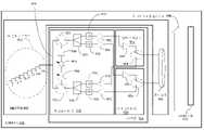
도 1은 본 발명에 따른 안테나 시스템의 구현 예의 시스템 블록도이다.
도 2는 본 발명에 따른, 도 1에 도시된 스위칭 가능한 송수신 페이즈드 어레이 안테나("STRPAA")의 구현 예의 블록도이다.
도 3은 본 발명에 따른, 도 2에 도시된 다층 인쇄 와이어링 보드("MLPWB")의 구현 예의 부분적 단면도이다.
도 4는 본 발명에 따른 MLPWB의 구현 예의 부분적 측면도이다.
도 5는 본 발명에 따른 MLPWB의 다른 구현 예의 부분적 측면도이다.
도 6은 본 발명에 따른, 도 2, 도 3, 도 4, 및 도 5에 도시된 방사 소자의 구현 예의 평면도이다.
도 7a는 본 발명에 따른, 도 2, 도 4 및 도 5에 도시된 허니콤 어퍼처 플레이트 레이아웃의 구현 예의 평면도이다.
도 7b는 도 7a에 도시된 허니콤 어퍼처 플레이트의 줌-인된 부분(zoomed-in portion)의 평면도이다.
도 8은 본 발명에 따른, 도 4 및 도 5에 도시된 RF 분배 네트워크의 구현 예의 평면도이다.
도 9는 본 발명에 따른 STRPAA의 다른 구현 예의 시스템 블록도이다.
도 10은 도 9에 도시된 T/R 모듈의 시스템 블록도이다.
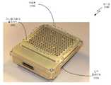
도 11은 본 발명에 따른, 도 2에 도시된 하우징의 오픈 구현 예의 예상도이다.
도 12는 도 11에 도시된 오픈 하우징의 다른 예상도이다.
도 13은 본 발명에 따른, WAIM 시트가 허니콤 어퍼처 플레이트의 위에 설치되지 않은, 도 11 및 도 12에 도시된 하우징의 클로즈드 하우징의 예상 평면도이다.
도 14는 본 발명에 따른, 허니콤 어퍼처 플레이트의 위에 설치된 WAIM 시트를 갖는, 도 11, 도 12, 및 도 13에 도시된 클로즈드 하우징의 예상 평면도이다.
도 15는 본 발명에 따른, 도 11, 도 12, 도 13, 및 도 14에 도시된 하우징의 구현 예의 분해된 예상 저면도이다.
도 16은 본 발명에 따른, 압력 플레이트의 내부 표면을 따르는, 도 11에 도시된 포켓들의 구현 예의 평면도이다.
도 17은 본 발명에 따른, 복수의 PCB(보드-대-보드) 전기 인터커넥트들과 결합되는, 도 2, 도 4, 도 5, 도 9, 도 10, 및 도 16에 도시된 T/R 모듈의 구현 예의 분해된 사시 측면도이다.
도 18은 도 17에 도시된 T/R 모듈의 분해된 사시 평면도이다.
도 19는 본 발명에 따른, 도 18에 도시된 모듈 캐리어에 설치된 제1 전력 스위칭 MMIC, 제2 전력 스위칭 MMIC, 및 빔 프로세싱 MMIC를 갖는 T/R 모듈의 사시 평면도이다.
도 20은 본 발명에 따른, 도 17, 도 18, 및 도 19에 도시된 T/R 모듈의 사시 저면도이다.
도 21은 본 발명에 따른, 송수신 모듈 세라믹 패키지("T/R 모듈 세라믹 패키지")의 구현 예의 부분적 단면도이다.
도 22는 본 발명에 따른, T/R 모듈 세라믹 패키지(2204)의 하단 표면 상의 인쇄 와이어링 어셈블리의 구현 예의 도면이다.
도 23은 본 발명에 따른, 도 22에 도시된 인쇄 와이어링 어셈블리 상으로의 빔 프로세싱 MMIC 및 전력 스위칭 MMIC들의 장착의 구현 예를 예시하는 도면이다.The present disclosure may be better understood by referring to the following figures. Components in the drawings are not necessarily to scale; instead, emphasis is made when illustrating the principles of the present disclosure. In the drawings, like reference numbers designate corresponding parts throughout the different views.
1 is a system block diagram of an example implementation of an antenna system according to the present invention.
FIG. 2 is a block diagram of an example implementation of a switchable transmit/receive phased array antenna (“STRPAA”) shown in FIG. 1 in accordance with the present invention.
FIG. 3 is a partial cross-sectional view of an example implementation of the multi-layer printed wiring board ("MLPWB") shown in FIG. 2, in accordance with the present invention.
4 is a partial side view of an example implementation of an MLPWB in accordance with the present invention.
5 is a partial side view of another implementation example of an MLPWB in accordance with the present invention.
6 is a plan view of an example implementation of the radiating element shown in FIGS. 2, 3, 4, and 5 in accordance with the present invention.
7A is a plan view of an example implementation of the honeycomb aperture plate layout shown in FIGS. 2, 4 and 5 in accordance with the present invention.
FIG. 7B is a plan view of a zoomed-in portion of the honeycomb aperture plate shown in FIG. 7A.
8 is a plan view of an example implementation of the RF distribution network shown in FIGS. 4 and 5 in accordance with the present invention.
9 is a system block diagram of another implementation example of STRPAA in accordance with the present invention.
FIG. 10 is a system block diagram of the T/R module shown in FIG. 9 .
11 is a projected view of an example of an open implementation of the housing shown in FIG. 2 according to the present invention.
FIG. 12 is another projected view of the open housing shown in FIG. 11;
Fig. 13 is a projected plan view of the closed housing of the housing shown in Figs. 11 and 12 without the WAIM sheet installed over the honeycomb aperture plate, according to the present invention;
14 is a projected plan view of the closed housing shown in FIGS. 11, 12, and 13 having a WAIM sheet installed over a honeycomb aperture plate, in accordance with the present invention.
15 is an exploded perspective bottom view of an embodiment of the housing shown in FIGS. 11, 12, 13, and 14, in accordance with the present invention;
16 is a plan view of an example implementation of the pockets shown in FIG. 11 along the inner surface of a pressure plate, in accordance with the present invention.
17 is a T/R module shown in FIGS. 2, 4, 5, 9, 10, and 16 coupled with a plurality of PCB (board-to-board) electrical interconnects, in accordance with the present invention. is an exploded perspective side view of an embodiment of
18 is an exploded perspective plan view of the T/R module shown in FIG. 17;
19 is a perspective plan view of a T/R module having a first power switching MMIC, a second power switching MMIC, and a beam processing MMIC installed in the module carrier shown in FIG. 18, in accordance with the present invention.
20 is a perspective bottom view of the T/R module shown in FIGS. 17, 18, and 19 according to the present invention.
21 is a partial cross-sectional view of an example implementation of a transmit/receive module ceramic package ("T/R module ceramic package") in accordance with the present invention.
22 is a diagram of an example implementation of a printed wiring assembly on the bottom surface of a T/R module ceramic package 2204, in accordance with the present invention.
23 is a diagram illustrating an example implementation of mounting the beam processing MMIC and power switching MMICs onto the printed wiring assembly shown in FIG. 22 in accordance with the present invention.
스위칭 가능한 송수신 페이즈드 어레이 안테나("STRPAA")가 개시된다. 예로서, STRPAA는 하우징, 상단 표면 및 하단 표면을 갖는, 이 하우징 내의 다층 인쇄 와이어링 보드("MLPWB"), MLPWB의 상단 표면 상에 위치된 복수의 방사 소자들, 및 MLPWB의 하단 표면에 부착된 복수의 송수신("T/R") 모듈들을 포함할 수 있다. 또한, STRPAA는 복수의 비아들을 포함할 수 있는데, 이 복수의 비아들의 각각의 비아는 MLPWB를 통과하고, 그리고 MLPWB의 하단 표면 상의 복수의 T/R 모듈들의 T/R 모듈과, MLPWB의 상단 표면 상에 위치된 복수의 방사 소자들 중 이 T/R 모듈에 대향하는 방사 소자 사이의 신호 경로로서 구성된다.A switchable transmit/receive phased array antenna (“STRPAA”) is disclosed. As an example, STRPAA includes a housing, a multilayer printed wiring board ("MLPWB") within the housing, having a top surface and a bottom surface, a plurality of radiating elements positioned on the top surface of the MLPWB, and attached to the bottom surface of the MLPWB. It may include a plurality of transmitted/received ("T/R") modules. STRPAA may also include a plurality of vias, each via of the plurality of vias passing through the MLPWB, and a T/R module of the plurality of T/R modules on the bottom surface of the MLPWB and the top surface of the MLPWB. It is configured as a signal path between radiating elements facing the T/R module among a plurality of radiating elements located on the upper part.
이 예에서, 복수의 T/R 모듈들은 MLPWB의 하단 표면과 신호 통신할 수 있고, 복수의 T/R 모듈들의 각각의 T/R 모듈은 MLPWB의 상단 표면 상에 위치된 복수의 방사 소자들 중 대응하는 방사 소자에 대향하게 MLPWB의 하단 표면 상에 위치될 수 있다. 부가하여, 하우징은 압력 플레이트, 그리고 복수의 채널들을 갖는 허니콤 어퍼처 플레이트를 포함할 수 있다.In this example, a plurality of T/R modules may be in signal communication with a bottom surface of the MLPWB, and each T/R module of the plurality of T/R modules is one of a plurality of radiating elements located on the top surface of the MLPWB. It can be positioned on the bottom surface of the MLPWB opposite the corresponding radiating element. In addition, the housing may include a pressure plate and a honeycomb aperture plate having a plurality of channels.
압력 플레이트는 MLPWB의 하단 표면에 맞닿게 복수의 T/R 모듈들을 밀어내도록 구성될 수 있다. 유사하게, 복수의 방사 소자들은 허니콤 어퍼처 플레이트에 거의 맞닿게 배치되도록 구성된다. 허니콤 어퍼처 플레이트에 맞닿게 배치될 때, 복수의 소자들의 각각의 방사 소자는 허니콤 어퍼처의 복수의 채널들 중 대응하는 채널에 위치된다.The pressure plate may be configured to push the plurality of T/R modules against the bottom surface of the MLPWB. Similarly, a plurality of radiating elements are configured to be disposed substantially in contact with the honeycomb aperture plate. When placed against the honeycomb aperture plate, each radiating element of the plurality of elements is positioned in a corresponding one of the plurality of channels of the honeycomb aperture.
이 예에서, STRPAA는 타일 구성을 포함하는 공통 어퍼처 페이즈드 어레이 안테나이다. T/R 모듈들은 평면 회로 구성을 활용할 수 있다.In this example, STRPAA is a common aperture phased array antenna that includes a tiled configuration. T/R modules may utilize planar circuit configurations.
도 1을 참조하면, 본 발명에 따라, 안테나 시스템(100)의 구현 예의 시스템 블록도가 도시된다. 이 예에서, 안테나 시스템(100)은 STRPAA(102), 제어기(104), 온도 제어 시스템(106), 및 전원(108)을 포함할 수 있다. STRPAA(102)는 신호 경로들(110, 112, 및 114)을 통해 각각 제어기(104), 온도 제어 시스템(106), 및 전원(108)과 신호 통신할 수 있다. 제어기(104)는 신호 경로들(116 및 118)을 통해 각각 전원(108) 및 온도 제어 시스템(106)과 신호 통신할 수 있다. 또한, 전원(108)은 신호 경로(120)를 통해 온도 제어 시스템(106)과 신호 통신한다.Referring to FIG. 1, a system block diagram of an example implementation of an antenna system 100, in accordance with the present invention, is shown. In this example, antenna system 100 may include
이 예에서, STRPAA(102)는 대응하는 방사 소자들을 갖는 복수의 T/R 모듈들을 포함하는 페이즈드 어레이 안테나("PAA")이고, 이들은, 결합하여, STRPAA(102)를 통해 신호들을 송신(122)하고 수신(124)할 수 있다. 이 예에서, STRPAA(102)는 K-대역 주파수 범위(즉, NATO K-대역의 경우 약 20 GHz 내지 40 GHz, 그리고 IEEE K-대역의 경우 18 GHz 내지 26.5 GHz) 내에서 동작하도록 구성될 수 있다.In this example, the
전원(108)은 안테나 시스템(100)의 다른 유닛들(즉, STRPAA(102), 제어기(104), 및 온도 제어 시스템(106))에 전력을 제공하는 디바이스, 컴포넌트, 및/또는 모듈이다. 부가하여, 제어기(104)는 안테나 시스템(100)의 동작을 제어하는 디바이스, 컴포넌트, 및/또는 모듈이다. 제어기(104)는 프로세서, 마이크로프로세서, 마이크로제어기, 디지털 신호 프로세서("DSP(digital signal processor)"), 또는 하드웨어 및/또는 소프트웨어 중 어느 쪽으로든 프로그래밍될 수 있는 다른 타입의 디바이스일 수 있다. 제어기(104)는 STRPAA(102)의 어레이 지향 각도, 편파(polarization), 태퍼(tapper), 및 STRPAA(102)의 일반적인 동작을 제어할 수 있다.
온도 제어 시스템(106)은 STRPAA(102) 상의 온도를 제어할 수 있는 디바이스, 컴포넌트, 및/또는 모듈이다. 동작 예에서, STRPAA(102)가 그것이 어떤 타입의 냉각을 필요로 하는 시점까지 뜨거워질 때, STRPAA(102)는 제어기(104), 온도 제어 시스템(106), 또는 둘 다에 이 필요성을 표시할 수 있다. 이 표시는 STRPAA(102)의 동작 온도를 측정하는, STRPAA(102) 내의 온도 센서의 결과일 수 있다. 일단 냉각의 필요성의 표시가 온도 제어 시스템(106)에 의해서든 또는 제어기(104)에 의해서든 수신되면, 온도 제어 시스템(106)은, 예컨대 에어 또는 액체 냉각을 통해, 필요로 되는 냉각을 STRPAA(102)에 제공할 수 있다. 유사한 방식으로, 온도 제어 시스템(106)은 또한, 전원(108)의 온도를 제어할 수 있다.
안테나 시스템(100)의, 또는 안테나 시스템(100)과 연관되는 회로들, 컴포넌트들, 모듈들, 및/또는 디바이스들이 서로 신호 통신하는 것으로서 설명되는데, 여기서 신호 통신은 회로, 컴포넌트, 모듈, 및/또는 디바이스가 다른 회로, 컴포넌트, 모듈, 및/또는 디바이스로부터의 신호들 및/또는 정보를 전달하고 그리고/또는 수신하도록 허용하는, 회로들, 컴포넌트들, 모듈들, 및/또는 디바이스들 사이의 임의의 타입의 통신 및/또는 연결을 지칭함이 당업자들에 의해 인식된다. 통신 및/또는 연결은, 신호들 및/또는 정보가 하나의 회로, 컴포넌트, 모듈, 및/또는 디바이스로부터 다른 회로, 컴포넌트, 모듈, 및/또는 디바이스로 전달되도록 허용하고 무선 또는 유선 신호 경로들을 포함하는, 회로들, 컴포넌트들, 모듈들, 및/또는 디바이스들 사이의 임의의 신호 경로를 따를 수 있다. 신호 경로들은 물리적일 수 있는데, 이를테면, 예컨대, 전도성 와이어들, 전자기파 가이드들, 케이블들, 부착된 그리고/또는 전자기인 또는 기계적으로 커플링된 단자들, 반도전성 또는 유전체 재료들 또는 디바이스들, 또는 다른 유사한 물리적 연결들 또는 커플링들일 수 있다. 부가하여, 신호 경로들은 자유-공간(전자기 전파의 경우)과 같이 비-물리적일 수 있거나, 또는 디지털 컴포넌트들을 통과하는 정보 경로들일 수 있는데, 여기서 통신 정보는, 직접적인 전자기 연결을 통과하지 않고, 다양한 디지털 포맷들로, 하나의 회로, 컴포넌트, 모듈, 및/또는 디바이스로부터 다른 회로, 컴포넌트, 모듈, 및/또는 디바이스로 전달된다.Circuits, components, modules, and/or devices of or associated with antenna system 100 are described as being in signal communication with one another, where signal communication is circuits, components, modules, and/or devices. or any intervening circuits, components, modules, and/or devices that allow a device to communicate and/or receive signals and/or information from another circuit, component, module, and/or device. It is recognized by those skilled in the art to refer to a type of communication and/or connection. Communication and/or connectivity allows signals and/or information to be transferred from one circuit, component, module, and/or device to another circuit, component, module, and/or device and includes wireless or wired signal paths. Any signal path between circuits, components, modules, and/or devices that Signal paths can be physical, such as, for example, conductive wires, electromagnetic wave guides, cables, attached and/or electromagnetically or mechanically coupled terminals, semiconducting or dielectric materials or devices, or It may be other similar physical connections or couplings. In addition, the signal paths can be non-physical, such as free-space (in the case of electromagnetic propagation), or they can be information paths through digital components, where the communication information does not pass through a direct electromagnetic connection, but can be various In digital formats, it is transferred from one circuit, component, module, and/or device to another circuit, component, module, and/or device.
도 2에서는, 본 발명에 따라, STRPAA(102)의 구현 예의 블록도가 도시된다. STRPAA(102)는 하우징(200), 압력 플레이트(202), 허니콤 어퍼처 플레이트(204), MLPWB(206), 복수의 방사 소자들(208, 210, 및 212), 복수의 T/R 모듈들(214, 216, 및 218), 및 광각 임피던스 매칭("WAIM(wide angle impedance matching)") 시트(220)를 포함할 수 있다. 이 예에서, 하우징(200)은 압력 플레이트(202) 및 허니콤 어퍼처 플레이트(204)의 결합에 의해 형성될 수 있다.2, a block diagram of an example implementation of
허니콤 어퍼처 플레이트(204)는 이 허니콤 어퍼처 플레이트(204)를 통과하는 복수의 채널들(220, 222, 및 224)을 포함하는 금속성 또는 유전체 구조 플레이트일 수 있는데, 여기서 복수의 채널들은 허니콤 어퍼처 플레이트(204)를 따라서 허니콤 구조를 정의한다. 이후, WAIM 시트(220)가 허니콤 어퍼처 플레이트(204)의 상단 또는 외부 표면에 부착된다. 일반적으로, WAIM 시트(220)는, STRPAA(102)의 개선된 스캐닝 성능을 가능하게 하기 위하여 STRPAA(102)와 자유 공간 사이의 임피던스 매치를 최적화시키고 리턴 손실을 최소화시키도록 선택 및 배열된 복수의 층들을 포함하는 비-전도성 재료의 시트이다.The
MLPWB(206)(다층 인쇄 회로 보드로서 또한 알려져 있음)는 인쇄 와이어링 보드("PWB")("PCB(printed circuit board)"로서 또한 알려져 있음)이며, PWB는 그 내부에서 다수의 트레이스 층들을 포함한다. 일반적으로, MLPWB(206)는 각각의 개별 PWB의 양면에 에칭된 회로를 포함할 수 있는 다수의 PWB들의 스택 업(stack up)인데, 여기서 다수의 PWB들을 함께 배치시키는데 라미네이션이 활용될 수 있다. 결과적 MLPWB는 신호 PWB 상에서보다 훨씬 더 높은 컴포넌트 밀도를 가능하게 한다.MLPWB 206 (also known as a multi-layer printed circuit board) is a printed wiring board ("PWB") (also known as a "printed circuit board"), the PWB having multiple trace layers therein. include In general, MLPWB 206 is a stack up of multiple PWBs, which may include circuitry etched on both sides of each individual PWB, where laminations may be utilized to place multiple PWBs together. The resulting MLPWB enables a much higher component density than on the signal PWB.
이 예에서, MLPWB(206)는 두 개의 표면들, 즉, 상단 표면(226) 및 하단 표면(228)을 갖고, 이들은 각각의 표면(226 및 228) 상에 에칭된 전기 트레이스들을 갖는다. 복수의 T/R 모듈들(214, 216, 및 218)이 MLPWB(206)의 하단 표면(228)에 부착될 수 있고, 복수의 방사 소자들(208, 210, 및 212)이 MLPWB(206)의 상단 표면(226)에 부착될 수 있다. 이 예에서, 복수의 T/R 모듈들(214, 216, 및 218)은, 복수의 전도성 전기 인터커넥트들(230, 232, 234, 236, 238, 240, 242, 244, 및 246)을 통해 각각 MLPWB(206)의 하단 표면(228)과 신호 통신할 수 있다.In this example, MLPWB 206 has two surfaces,
일 실시예에서, 전기 인터커넥트들은 "fuzz buttons®"로서 구현될 수 있다. 일반적으로, "fuzz button®"이, 통상적으로 범위가 일 밀리미터의 몇 십분의 일 내지 일 밀리미터에 이르는 특정 지름의 치밀한 원통형 재료로 형성되는 금-도금된 베릴륨 구리 와이어의 단일 가닥으로 만들어지는 고성능 "신호 콘택"임이 당업자들에 의해 인식된다. 그들은 종종 반도체 테스트 소켓들 및 PWB 인터커넥트들에서 활용되는데, 여기서 저-왜곡 송신 라인들이 필수품이다. 다른 실시예에서, 전기 인터커넥트들은, 솔더에 의해, 영구 콘택들을 형성하도록 리플로우될 수 있는 솔더 볼들의 볼 그리드 어레이를 활용하여 구현될 수 있다.In one embodiment, electrical interconnects may be implemented as “fuzz buttons®”. Generally, a "fuzz button®" is a high performance "fuzz button®" made from a single strand of gold-plated beryllium copper wire formed from a dense cylindrical material of a specific diameter, typically ranging from tenths of a millimeter to one millimeter. signal contact" is recognized by those skilled in the art. They are often utilized in semiconductor test sockets and PWB interconnects, where low-distortion transmission lines are a necessity. In another embodiment, electrical interconnects may be implemented utilizing a ball grid array of solder balls that can be reflowed by solder to form permanent contacts.
방사 소자들(208, 210, 및 212)은 MLPWB(206)의 상단 표면(226)에 부착되는 별개의 모듈들, 디바이스들, 및/또는 컴포넌트들일 수 있거나, 또는 이 방사 소자들(208, 210, 및 212)은 실제로는, MLPWB(206)의 상단 표면(226)의 표면 상의 에칭된 소자들로서 MLPWB(206)의 일부일 수 있다(이를테면, 예컨대, 마이크로스트립/패치 안테나 소자). 별개의 모듈들의 경우, 전기 인터커넥트들(미도시)의 사용을 비롯해 MLPWB(206)의 하단 표면(228) 상에 복수의 T/R 모듈들(214, 216, 및 218)을 부착할 때 활용되는 것과 동일한 기술들을 활용하여, 방사 소자들(208, 210, 212)이 MLPWB(206)의 상단 표면(226)에 부착될 수 있다.The radiating
어느 경우에나, 복수의 방사 소자들(208, 210, 및 212)은 MLPWB(206)를 통과하는 복수의 전도성 채널들(본원에서, "비아" 또는 "비아들"로서 지칭됨)(248, 250, 252, 254, 256, 및 258)을 통해 각각 복수의 T/R 모듈들(214, 216, 및 218)과 신호 통신한다. 이 예에서, 각각의 방사 소자(208, 210, 및 212)는 MLPWB(206)의 대향하는 표면 상에 위치되는, 대응하는 개별 T/R 모듈(214, 216, 및 218)과 신호 통신한다. 부가하여, 각각의 방사 소자(208, 210, 및 212)는 개별 채널(220, 222, 및 224)에 대응할 것이다. 비아들(248, 250, 252, 254, 256, 및 258)은 전도성의 금속성 및/또는 유전체 재료를 포함할 수 있다. 동작 시, 방사 소자들은 무선 신호들, 이를테면, 예컨대, K-대역 신호들을 송신 및/또는 수신할 수 있다.In either case, the plurality of radiating
용어 "비아" 또는 "비아들"이 잘 알려져 있음이 당업자들에 의해 인식된다. 구체적으로, 비아는, 하나 또는 그 초과의 인접한 층들의 평면을 통과하는, 물리적 전자 회로의 층들 간 전기 연결인데, 이 예에서는, MLPWB(206)가 물리적 전자 회로이다. 물리적으로, 비아는, MLPWB(206)의 상이한 층들 간의 전도성 연결을 허용하는, 절연 층의 소형 전도성 홀이다. 이 예에서, 비아들(248, 250, 252, 254, 256, 및 258)은 MLPWB(206)의 하단 표면(228)으로부터 MLPWB(206)의 상단 표면(226)으로 연장되는 개별 비아들로서 도시되지만, 각각의 개별적인 비아가 실제로는, MLPWB(206)의 개별적인 다수의 층들을 서로 개별적으로 연결시키는 다수의 서브-비아들을 포함하는 결합 비아일 수 있다.It is recognized by those skilled in the art that the term “via” or “vias” is well known. Specifically, a via is an electrical connection between layers of a physical electronic circuit that passes through the plane of one or more adjacent layers, in this example MLPWB 206 being the physical electronic circuit. Physically, a via is a small conductive hole in an insulating layer that allows a conductive connection between different layers of MLPWB 206 . In this example, vias 248, 250, 252, 254, 256, and 258 are shown as individual vias extending from
또한, MLPWB(206)는 MLPWB(206)의 층들 내에 라디오 주파수("RF(radio frequency)") 분배 네트워크(미도시)를 포함할 수 있다. RF 분배 네트워크는, RF 신호들을 복수의 T/R 모듈들의 개별 T/R 모듈들로 분배하기 위해 단일 경로들을 사용하는 공동의 피드 네트워크일 수 있다. 예로서, RF 분배 네트워크는 복수의 스트립라인 소자들 및 윌킨슨 전력 결합기들/분배기들을 포함할 수 있다.MLPWB 206 may also include a radio frequency ("radio frequency") distribution network (not shown) within the layers of MLPWB 206 . An RF distribution network may be a common feed network that uses single paths to distribute RF signals to individual T/R modules of a plurality of T/R modules. As an example, an RF distribution network may include a plurality of stripline elements and Wilkinson power combiners/dividers.
예시의 단순성의 목적들을 위해, 단 세 개의 방사 소자들(208, 210, 212) 및 세 개의 T/R 모듈들(214, 216, 및 218)만이 도시됨이 당업자들에 의해 인식된다. 또한, 단 세 개의 채널들(220, 222, 및 224)만이 도시된다. 그러나, 도 2에서 구체적으로 도시되는 것보다 더 많은 방사 소자들, T/R 모듈들, 및 채널들이 존재할 수 있음이 인식된다. 예로서, STRPAA(102)는 256개의 어레이 소자들을 갖는 PAA를 포함할 수 있는데, 이는 STRPAA(102)가 256개의 방사 소자들, 256개의 T/R 모듈들, 및 허니콤 어퍼처 플레이트(204)를 통과하는 256개의 채널들을 포함할 것임을 의미할 것이다.For purposes of simplicity of illustration, it will be appreciated by those skilled in the art that only three radiating
부가하여, 방사 소자들(208, 210, 및 212)과 T/R 모듈들(214, 216, 및 218)의 결합 쌍마다 단 두 개의 비아들(248, 250, 252, 254, 256, 및 258)만이 도시됨이 또한 인식된다. 이 예에서, 결합 쌍마다의 제1 비아는 제1 편파 신호에 대한 신호 경로에 대응할 수 있고, 결합 쌍마다의 제2 비아는 제2 편파 신호에 대한 신호 경로에 대응할 수 있다. 그러나, 결합 쌍마다 부가적인 비아들이 존재할 수 있음이 인식된다.In addition, only two
이 예에서, 허니콤 어퍼처 플레이트(204)를 다시 참조하면, 채널들(220, 222, 및 224)은 대응하는 방사 소자들(208, 210, 및 212)에 대한 도파관들로서 동작한다. 그로 인해서, 채널들(220, 222, 및 224)은 에어, 가스, 또는 유전체로 필링될 수 있다.Referring back to
압력 플레이트(202)는 내부 표면(260)을 포함하는 하우징(200)의 일부일 수 있고, 이 내부 표면(260)은, 복수의 T/R 모듈들(214, 216, 및 218)의 하단을 위쪽으로 밀고(butt up) MLPWB(206)의 하단 표면(228)에 맞닿게 이 복수의 T/R 모듈들(214, 216, 및 218)을 밀어낸다. 압력 플레이트(202)는 또한, 내부 표면(260)을 따라서 복수의 압축 스프링들(미도시)을 포함할 수 있고, 이 복수의 압축 스프링들은, MLPWB(206)의 하단 표면(228)에 맞닿게 T/R 모듈들(214, 216, 및 218)을 밀어내기 위해, 이 T/R 모듈들(214, 216, 및 218)의 하단들에 부가적인 힘을 가한다.The
도 3에서는, 본 발명에 따라, MLPWB(300)의 구현 예의 부분적 단면도가 도시된다. MLPWB(300)는 도 2에 도시된 MLPWB(206)의 예이다. 이 예에서, MLPWB(300)는, 본딩 층(306)을 활용하여 서로 본딩되는 두 개의 PWB 서브-어셈블리들(302 및 304)을 포함할 수 있다.In FIG. 3, a partial cross-sectional view of an example implementation of an
본딩 층(306)은, 비아(307)와 비아(308)를 서로 전기적으로 연결시키고 비아(309 및 310)를 서로 전기적으로 연결시키기 위해 기계적 본딩 뿐만 아니라 전기 특성들을 제공한다. 예로서, 본딩 층(306)은 본딩 재료, 예컨대, 캘리포니아 샌 디에고의 Ormet Circuits, Inc.®에 의해 제공되는 본딩 재료들, 예컨대, FR-408HR로 만들어질 수 있다. 본딩 층(306)의 두께는, 예컨대, 대략 4mil(1인치의 1/1000)일 수 있다.
이 예에서, 제1 PWB 서브-어셈블리(302)는 아홉(9) 개의 기판들(311, 312, 313, 314, 315, 316, 317, 318, 및 319)을 포함할 수 있다. 부가하여, 열(10) 개의 금속성 층들(예컨대, 구리)(320, 321, 322, 323, 324, 325, 326, 327, 328, 및 329)이 이 아홉 개의 기판들(311, 312, 313, 314, 315, 316, 317, 318, 및 319)을 서로 격리시킨다. 유사하게, 제2 PWB 서브-어셈블리(304)가 또한, 아홉(9) 개의 기판들(330, 331, 332, 333, 334, 335, 336, 337, 및 338)을 포함할 수 있다. 부가하여, 열(10) 개의 금속성 층들(예컨대, 구리)(339, 340, 341, 342, 343, 344, 345, 346, 347, 및 348)이 이 아홉 개의 기판들(330, 331, 332, 333, 334, 335, 336, 337, 및 338)을 서로 격리시킨다. 이 예에서, 본딩 층(306)은 금속성 층(320)을 금속성 층(348)에 본딩한다.In this example, the
이 예에서, 도 2에 설명된 예와 유사하게, 방사 소자(350)는 MLPWB(300)의 상단 표면(351)에 부착된 것으로서 도시되고, T/R 모듈(352)은 MLPWB(300)의 하단 표면(353)에 부착된 것으로 도시된다. 이 상단 표면(351)은 금속성 층(329)의 상단 표면에 대응하고, 이 하단 표면(353)은 금속성 층(339)의 하단 표면에 대응한다. 도 2에서와 같이, T/R 모듈(352)은 비아들(307 및 308)과 비아들(309 및 310)의 결합을 통해 방사 소자(350)와 신호 통신하는 것으로 도시되는데, 여기서 비아들(307 및 308)은 본딩 층(306)을 통해 신호 통신하고, 비아들(309 및 310)은 또한 본딩 층(306)을 통해 신호 통신한다. 비아(307)가 서브-비아들("매립된 비아들"로서 또한 알려져 있음)(354, 355, 356, 357, 358, 359, 360, 361, 및 362)을 포함할 수 있고, 비아(308)가 서브-비아들(363, 364, 365, 366, 367, 368, 369, 370, 및 371)을 포함할 수 있음이 인식된다. 유사하게, 비아(309)는 서브-비아들("매립된 비아들"로서 또한 알려져 있음)(372, 373, 374, 375, 376, 377, 378, 379, 및 380)을 포함할 수 있고, 비아(310)는 서브-비아들(381, 382, 383, 384, 385, 386, 387, 388, 및 389)을 포함할 수 있다. 이 예에서, 금속성 층들(320, 321, 322, 323, 324, 325, 326, 327, 328, 329, 339, 340, 341, 342, 343, 344, 345, 346, 347, 및 348)은 전기적으로 접지된 층들일 수 있다. 이들은 대략 0.7 내지 2.8 mils 사이에서 변하는 두께를 가질 수 있다. 기판들(311, 312, 313, 314, 315, 316, 317, 318, 319, 330, 331, 332, 333, 334, 335, 336, 337, 및 338)은, 예컨대, 코네티컷의 로저스의 Rogers Corporation®에 의해 생산되는 RO4003C, RO4450F, 및 RO4450B의 결합일 수 있다. 기판들(311, 312, 313, 314, 315, 316, 317, 318, 319, 330, 331, 332, 333, 334, 335, 336, 337, 및 338)은 대략 4.0 내지 16.0 mils 사이에서 변하는 두께를 가질 수 있다.In this example, similar to the example described in FIG. 2 , radiating
이 예에서, 통상적인 아키텍처들에서 이루어졌던 바와 같이 비아들의 단일 쌍이 전체 MLPWB(300)를 관통하게 하는 것과는 대조적으로, 비아들(307 및 308) 및 비아들(309 및 310)의 지름들은 감소될 수 있다. 이러한 방식으로, MLPWB(300)에 대한 설계들 및 아키텍처들의 크기는, 방사 소자들(예컨대, 방사 소자(350))에 대한 회로를 더욱 들어맞게 하기 위해 크기가 감소될 수 있다. 그로 인해서, 이 접근법에서, MLPWB(300)는 더 많은 그리고/또는 더욱 소형의 방사 소자들이 MLPWB(300)의 상단 표면(351) 상에 배치되도록 허용할 수 있다.In this example, the diameters of
예컨대, 앞서 진술된 바와 같이, 방사 소자(350)는 MLPWB(300)의 상단 표면(351) 상에 또는 이 상단 표면(351) 내에 형성될 수 있다. T/R 모듈(352)은 전기 인터커넥트 신호 콘택들을 활용하여 MLPWB(300)의 하단 표면(353) 상에 장착될 수 있다. 이러한 방식으로, T/R 모듈(352)을 방사 소자(350)에 연결시키는 신호 경로에서 90도 각도 또는 굴곡을 요구하지 않는 방식으로, 방사 소자(350)는 대응하는 T/R 모듈(352)에 대향하게 위치될 수 있다. 더욱 구체적으로, 방사 소자(350)가 실질적으로 T/R 모듈(352)과 정렬될 수 있어, 비아들(307, 308, 309, 및 310)은 방사 소자(350)와 T/R 모듈 사이에서 직선 경로를 형성한다.For example, as stated above, the radiating
도 4를 참조하면, 본 발명에 따라, MLPWB(400)의 구현 예의 부분적 측면도가 도시된다. MLPWB(400)는 도 2에 도시된 MLPWB(206) 및 도 3에 도시된 MLPWB(300)의 예이다. 이 예에서, MLPWB(400)는 단지, 도 2의 MLPWB(300)에 도시된 스무(20) 개의 기판 층들 대신에 세(3) 개의 기판 층들(402, 404, 및 406)을 도시한다. 단 두(2) 개의 금속성 층들(408 및 410)만이 기판(404) 주위에 도시된다. 부가하여, 본딩 층은 도시되지 않는다. T/R 모듈(412)이 홀더(416)를 통해 MLPWB(400)의 하단 표면(414)에 부착된 것으로 도시되고, 이 홀더(416)는 복수의 전기 인터커넥트 신호 콘택들(418, 420, 422, 및 424)을 포함한다. 전기 인터커넥트 신호 콘택들(418, 420, 422, 및 424)은 MLPWB(400)의 하단 표면(414) 상의 복수의 형성된 그리고/또는 에칭된 콘택 패드들(426, 428, 430, 및 432)과 각각 신호 통신할 수 있다.Referring to FIG. 4, a partial side view of an example implementation of an
이 예에서, 방사 소자(434)가 MLPWB(400) 내에서 기판 층(406)에 형성된 것으로 도시되고, 이 방사 소자(434)는 인쇄 안테나로서 구현될 수 있다. 이 방사 소자(434)는 층(406) 내로 에칭될 수 있는 두 개의 방사기들(436 및 438)을 갖는 것으로 도시된다. 예로서, 제1 방사기(436)는 제1 타입의 편파(이를테면, 예컨대, 수직 편파 또는 오른손방향 원형 편파)를 방사할 수 있고, 제2 방사기(438)는 제1 편파와 직교하는 제2 타입의 편파(이를테면, 예컨대, 수평 편파 또는 왼손방향 원형 편파)를 방사할 수 있다. 또한, 방사 소자(434)는, 방사 소자의 지향성을 개선시키고 그리고/또는 방사 소자의 상호 커플링을 감소시키기 위해, 접지, 반사, 및/또는 격리 소자들(440)을 포함할 수 있다. 제1 방사기(436)는 제1 비아(444)를 통해 콘택 패드(426)와 신호 통신하는 제1 프로브(442)에 의해 피딩될 수 있고, 이 콘택 패드(426)는 전기 인터커넥트 신호 콘택(418)을 통해 T/R 모듈(412)과 신호 통신한다. 유사하게, 제2 방사기(438)는 제2 비아(448)를 통해 콘택 패드(428)와 신호 통신하는 제2 프로브(446)에 의해 피딩될 수 있고, 이 콘택 패드(428)는 전기 인터커넥트 신호 콘택(420)을 통해 T/R 모듈(412)과 신호 통신한다. 이 예에서, 제1 비아(444)는, 방사 소자(434)의 아키텍처가 기판 층(406)에서 어떻게 설계되는지에 기초하여, 제1 프로브(442)의 일부 또는 전부일 수 있다. 유사하게, 제2 비아(448)는 또한, 제2 프로브(446)의 일부 또는 전부일 수 있다.In this example, a radiating
이 예에서, RF 분배 네트워크(450)가 도시된다. RF 커넥터(452)가 또한, MLPWB(400)의 하단 표면(414) 상의 콘택 패드(454)를 통해 RF 분배 네트워크(450)와 신호 통신하는 것으로 도시된다. 앞서 논의된 바와 같이, RF 분배 네트워크(450)는 복수의 전력 결합기 및/또는 분배기들(이를테면, 예컨대, 윌킨슨 전력 결합기들)과 스트립라인 단자들을 포함하는 스트립라인 분배 네트워크일 수 있다. RF 분배 네트워크(450)는 MLPWB(400)의 하단 표면(414)에 부착된 복수의 T/R 모듈들에 피딩하도록 구성된다. 이 예에서, RF 커넥터(452)는 SMP-스타일 미니어처 푸쉬-온 커넥터, 이를테면, 예컨대, 애리조나 글렌데일의 Corning Gilbert Inc.®에 의해 생산되는 G3PO® 타입 커넥터, 또는 포트 임피던스가 대략 50 오옴인 다른 균등한 고주파수 커넥터들일 수 있다.In this example, an
이 예에서, 허니콤 어퍼처 플레이트(454)가 또한, MLPWB(400)의 상단 표면(456)에 인접하게 배치된 것으로 도시된다. 허니컴 어퍼처 플레이트(454)는 도 2에 도시된 허니콤 어퍼처 플레이트(204)의 부분도이다. 허니콤 어퍼처 플레이트(454)는 방사 소자(434)에 인접하게 위치되는 채널(458)을 포함한다. 이 예에서, 채널(458)은 원통형일 수 있고, 방사 소자(434)에 대한 원형 도파관 혼(circular waveguide horn)으로서 동작할 수 있다. 허니콤 어퍼처 플레이트(454)는 에어 갭(461)을 형성하기 위해 MLPWB(400)의 상단 표면(456)으로부터 떨어져 작은 거리(460)만큼 이격될 수 있고, 이 에어 갭(461)은 결합된 방사 소자(434) 및 채널(458)의 방사 성능을 튜닝하는데 활용될 수 있다. 예로서, 에어 갭(461)은 대략 0.005 인치인 폭(460)을 가질 수 있다. 이 예에서, 방사 소자(434)는 접지 소자들(440)을 포함하고, 이 접지 소자들(440)은 (466과 468 사이의 갭을 가리키는,) 콘택 패드들(466 및 468)을 통해 허니콤 어퍼처 플레이트(454)의 하단 표면(462)과 신호 통신하게 배치되는 접지 콘택들로서 동작하며, 이 콘택 패드들(466 및 468)은 MLPWB(400)의 상단 표면(456)으로부터 돌출하고 허니콤 어퍼처 플레이트(454)의 하단 표면(462)을 압박한다. 이러한 방식으로, 채널(458)의 내벽들(464)이 접지되고, 콘택 패드들(466 및 468)의 높이가 에어 갭(461)의 폭(460)에 대응한다.In this example, a
도 4와 유사하게, 도 5에서는, 본 발명에 따라, MLPWB(500)의 다른 구현 예의 부분적 측면도가 도시된다. MLPWB(500)는 도 2에 도시된 MLPWB(206), 도 3에 도시된 MLPWB(300), 및 도 4에 도시된 MLPWB(400)의 예이다. 이 예에서, MLPWB(500)는 단지, 도 3의 MLPWB(300)에 도시된 스무(20) 개의 기판 층들 대신에 네(4) 개의 기판 층들(502, 504, 506, 및 508)을 나타낸다.Similar to FIG. 4 , in FIG. 5 , a partial side view of another implementation of an
단 세(3) 개의 금속성 층들(510, 512, 및 514)만이 기판들(504 및 506) 주위에 도시된다. 부가하여, 본딩 층은 도시되지 않는다. T/R 모듈(516)이 홀더(520)를 통해 MLPWB(500)의 하단 표면(518)에 부착된 것으로 도시되고, 이 홀더(520)는 복수의 전기 인터커넥트 신호 콘택들(522, 524, 526, 및 528)을 포함한다. 전기 인터커넥트 신호 콘택들(522, 524, 526, 및 528)은 MLPWB(500)의 하단 표면(518) 상의 복수의 형성된 그리고/또는 에칭된 콘택 패드들(530, 532, 534, 및 536)과 각각 신호 통신할 수 있다.Only three (3)
이 예에서, 방사 소자(538)는 MLPWB(500) 내에서 기판 층(508)에, 층(508) 내로 에칭될 수 있는 마이크로스트립 안테나와 같이 형성되는 것으로 도시된다. 도 4와 유사하게, 방사 소자(538)는 두 개의 방사기들(540 및 542)을 갖는 것으로 도시된다. 다시, 도 4에 설명된 예에서와 같이, 제1 방사기(540)는 제1 타입의 편파(이를테면, 예컨대, 수직 편파 또는 오른손방향 원형 편파)를 방사할 수 있고, 제2 방사기(542)는 제1 편파에 직교하는 제2 타입의 편파(이를테면, 예컨대, 수평 편파 또는 왼손방향 원형 편파)를 방사할 수 있다. 방사 소자(538)는 또한, 접지 소자들(544)을 포함할 수 있다. 제1 방사기(540)는 제1 비아(548)를 통해 콘택 패드(530)와 신호 통신하는 제1 프로브(546)에 의해 피딩될 수 있고, 이 콘택 패드(530)는 전기 인터커넥트 신호 콘택(522)을 통해 T/R 모듈(516)과 신호 통신한다. 유사하게, 제2 방사기(542)는 제2 비아(552)를 통해 콘택 패드(532)와 신호 통신하는 제2 프로브(550)에 의해 피딩될 수 있고, 이 콘택 패드(532)는 전기 인터커넥트 신호 콘택(524)을 통해 T/R 모듈(516)과 신호 통신한다. 도 4에 설명된 예와는 달리, 이 예에서는, 제1 비아(548) 및 제2 비아(552)는 부분적으로 각각, 제1 프로브(546) 및 제2 프로브(550)의 일부이다. 부가하여, 이 예에서, 제1 프로브(546) 및 제2 프로브(550)는 기판(506)에서 90도의 굴곡부들을 포함한다.In this example, the radiating
도 4의 예와 유사하게, 이 예에서, RF 분배 네트워크(554)가 또한 도시된다. 또한, RF 커넥터(556)는 MLPWB(500)의 하단 표면(518) 상의 콘택 패드(558)를 통해 RF 분배 네트워크(554)와 신호 통신하는 것으로 도시된다. 다시, RF 분배 네트워크(554)는 MLPWB(500)의 하단 표면(518)에 부착되는 복수의 T/R 모듈들에 피딩하도록 구성된다. 이 예에서, RF 커넥터(556)는 또한, SMP-스타일 미니어처 푸쉬-온 커넥터, 이를테면, 예컨대, G3PO® 타입 커넥터, 또는 포트 임피던스가 대략 50 오옴인 다른 균등한 고주파수 커넥터들일 수 있다.Similar to the example of FIG. 4 , in this example, an
이 예에서, 허니콤 어퍼처 플레이트(560)는 또한, MLPWB(500)의 상단 표면(562)에 인접하게 배치된 것으로 도시된다. 다시, 허니콤 어퍼처 플레이트(560)는 도 2에 도시된 허니콤 어퍼처 플레이트(204)의 부분도이다. 허니콤 어퍼처 플레이트(560)는 채널(564)을 포함하고, 이 채널(564)은 방사 소자(538)에 인접하게 위치된다. 다시, 이 채널(564)은 원통형일 수 있고, 방사 소자(538)에 대한 원형 도파관 혼으로서 동작할 수 있다. 또한, 허니콤 어퍼처 플레이트(560)는 에어 갭(568)을 형성하기 위해 MLPWB(500)의 상단 표면(562)으로부터 떨어져 짧은 거리(566)만큼 이격될 수 있고, 이 에어 갭(568)은 결합된 방사 소자(538) 및 채널(564)의 방사 성능을 튜닝하는데 활용될 수 있다. 예로서, 이 에어 갭(568)은 대략 0.005 인치인 폭(566)을 가질 수 있다. 이 예에서, 접지 소자들(544)은 콘택 패드들(572 및 574)을 통해 허니콤 어퍼처 플레이트(560)의 하단 표면(570)과 신호 통신하게 배치되는 접지 콘택들로서 동작하고, 이 콘택 패드들(572 및 574)은 MLPWB(500)의 상단 표면(562)으로부터 돌출하고 허니콤 어퍼처 플레이트(560)의 하단 표면(570)을 압박한다. 이러한 방식으로, 채널(564)의 내벽들(576)이 접지되고, 콘택 패드들(572 및 574)의 높이는 에어 갭(568)의 폭(566)에 대응한다.In this example,
도 6을 참조하면, 위에서 설명된 MLPWB들(206, 300, 400, 또는 500) 중 임의의 MLPWB와 함께 사용될 수 있는 방사 소자(600)의 구현 예의 평면도가 도시된다. 이 예에서, 방사 소자(600)는 MLPWB의 상단 표면(602) 상에 형성되고 그리고/또는 에칭된다. 도 4 및 도 5에 설명된 바와 같이, 방사 소자(600)는 제1 방사기(604) 및 제2 방사기(606)를 포함할 수 있다. 도 4 및 도 5에서 앞서 설명된 바와 같이, 제1 방사기(604)는 T/R 모듈(미도시)과 신호 통신하는 제1 프로브(미도시)에 의해 피딩되고, 제2 방사기(606)는 T/R 모듈(미도시)과 또한 신호 통신하는 제2 프로브(미도시)에 의해 피딩된다. 앞서 설명된 바와 같이, 제1 방사기(604)는 제1 타입의 편파(이를테면, 예컨대, 수직 편파 또는 오른손방향 원형 편파)를 방사할 수 있고, 제2 방사기(606)는 제1 편파에 직교하는 제2 타입의 편파(이를테면, 예컨대, 수평 편파 또는 왼손방향 원형 편파)를 방사할 수 있다. 또한, 이 예에서는, 도 4 및 도 6에 설명된 소자들 또는 접지 소자(608)가 도시된다. 접지 소자(들)(608)는 복수의 콘택 패드들(미도시)을 포함할 수 있고, 이 콘택 패드들이 MLPWB의 상단 표면(602)으로부터 밖으로 돌출하여 허니콤 어퍼처 플레이트(미도시)의 하단 표면(미도시)에 맞물려, 방사 소자(600)에 인접하게 위치되는 채널(미도시)의 벽들을 적절하게 접지시킨다. 부가하여, 접지 비아(610)가 방사기 대역폭을 튜닝하는 것을 돕기 위한 방사 소자(600)일 수 있다.Referring to FIG. 6 , a top view of an example implementation of a
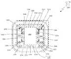
도 7a에서는, 본 발명에 따라, 허니컴 어퍼처 플레이트(700)의 구현 예의 평면도가 도시된다. PAA의 래티스 구조로 분포된 복수의 채널들(702)을 갖는 허니컴 어퍼처 플레이트(700)가 도시된다. 이 예에서, STRPAA는 256개 소자의 PAA를 포함할 수 있고, 이 256개 소자의 PAA는 256개의 채널들(702)을 갖는 허니콤 어퍼처 플레이트(700)를 야기할 것이다. 256개 소자의 PAA에 기초하여, PAA의 래티스 구조는 16 × 16개의 소자들을 갖는 PAA를 포함할 수 있고, 이는 허니콤 어퍼처 플레이트(700)를 따라서 분포된 16 × 16개 채널들(702)을 갖는 허니콤 어퍼처 플레이트(700)를 야기할 것이다.In FIG. 7A , a plan view of an example implementation of a
도 7b를 참조하면, 허니콤 어퍼처 플레이트(700)의 줌-인된 부분(704)의 평면도가 도시된다. 이 예에서, 줌-인된 부분(704)은 래티스로 분포된 세(3) 개의 채널들(706, 708, 및 710)을 포함할 수 있다. 이 예에서, 채널들(706, 708, 및 710)의 지름들이 대략 0.232 인치와 동일하고, 채널들(706, 708, 및 710)의 유전율("εr")이 대략 2.5와 동일하고, STRPAA가 (채널들(706, 708, 및 710)에 의해 형성된 도파관들에 대해) 대략 18.75 GHz의 도파관 컷오프 주파수를 갖는, 21 GHz 내지 22 GHz의 주파수 범위에서 동작하는 K-대역 안테나이면, x축(714)에서(즉, 제1 채널(706)의 중심과 제2 및 제3 채널들(708 및 710)의 중심 간)의 거리(712)는 대략 0.302 인치와 동일할 수 있고, y축(718)에서(즉, 제2 채널(708)의 중심과 제3 채널(710)의 중심 간)의 거리(716)는 대략 0.262 인치와 동일할 수 있다.Referring to FIG. 7B , a top view of a zoomed-in
도 8에서는, 본 발명에 따라, RF 분배 네트워크(800)의 구현 예의 평면도가 도시된다. RF 분배 네트워크(800)는 RF 커넥터(802)(이 RF 커넥터(802)는 도 4 및 도 5에서 앞서 설명된 RF 커넥터들(452 또는 556)와 같은 RF 커넥터의 예임) 및 복수의 T/R 모듈들과 신호 통신한다. 이 예에서, RF 분배 네트워크(800)는, 송신 모드에서 RF 커넥터(802)로부터의 입력 신호를, 개별적인 256개의 T/R 모듈들에 피딩되는 256개의 하위-신호들로 분할하도록 구성되는 16 × 16 분배 네트워크이다. 수신 모드에서, RF 분배 네트워크(800)는, 256개의 T/R 모듈들로부터 256개의 개별적인 신호들을 수신하여 이들을, RF 커넥터(802)에 전달되는 결합 출력 신호로 결합하도록 구성된다. 이 예에서, 도 4 및 도 5에서 앞서 설명된 바와 같이, RF 분배 네트워크는 양방향 윌킨슨 전력 결합기들/분배기들의 여덟 개의 스테이지들(804, 806, 808, 및 810)을 포함할 수 있고, RF 분배 네트워크는 MLPWB(812) 또는 MLPWB들(206, 300, 400, 500)의 내부 층으로 통합될 수 있다.8, a top view of an example implementation of an RF distribution network 800, in accordance with the present invention, is shown. The RF distribution network 800 includes an RF connector 802 (which is an example of an RF connector, such as
도 9를 참조하면, 본 발명에 따라, STRPAA(900)의 다른 구현 예의 시스템 블록도가 도시된다. 도 2와 유사하게, 도 9에서, STRPAA(900)는 MLPWB(902), T/R 모듈(904), 방사 소자(906), 허니콤 어퍼처 플레이트(908), 및 WAIM 시트(910)를 포함할 수 있다. 이 예에서, MLPWB(902)는 RF 분배 네트워크(912) 및 방사 소자(906)를 포함할 수 있다. RF 분배 네트워크(912)는 양방향 윌킨슨 전력 결합기들/분배기들의 여덟 개의 스테이지들을 갖는, 256개 소자(즉, 16 × 16)의 분배 네트워크일 수 있다.Referring to FIG. 9 , a system block diagram of another implementation of
T/R 모듈(904)은 두 개의 전력 스위칭 집적 회로들("IC(integrated circuit)들")(914 및 916) 및 빔 프로세싱 IC(918)를 포함할 수 있다. 스위칭 IC들(914 및 916) 및 빔 프로세싱 IC(918)는 모놀리식 마이크로파 집적 회로들("MMIC(monolithic microwave integrated circuit)들")일 수 있고, 이들은 "플립-칩(flip-chip)" 패키징 기술들을 활용하여 서로 신호 통신하게 배치될 수 있다.The T/
일반적으로, 플립-칩 패키징 기술들은 칩 패드들(즉, 칩 콘택들) 상에 증착된 골드 스터드 범프들 또는 솔더 범프들을 활용하여 반도체 디바이스들, 예컨대, 집적 회로들 "칩들" 및 마이크로전자기계 시스템("MEMS(microelectromechanical system)")들을 외부 회로에 상호연결시키기 위한 방법인 것으로 당업자들에 의해 인식된다. 일반적으로, 범프들은 최종 웨이퍼 프로세싱 단계 동안 웨이퍼의 상단 면 상의 칩 패드들 상에 증착된다. 칩을 외부 회로(예컨대, 회로 보드 또는 다른 칩 또는 웨이퍼)에 장착하기 위하여, 이 칩은, 이 칩의 상단 면이 아래로 향하도록 뒤집히고, 이 칩의 패드들이 외부 회로 상의 매칭 패드들과 정렬하도록 정렬되고, 이후, 솔더가 리플로우되거나 또는 스터드 범프가 열적으로 압축되어, 인터커넥트가 완성된다. 이는, 칩이 수직으로 장착되고 그리고 칩 패드들을 외부 회로에 상호연결시키는데 와이어들이 사용되는 와이어 본딩과는 대조적이다.In general, flip-chip packaging techniques utilize gold stud bumps or solder bumps deposited on chip pads (ie, chip contacts) to form semiconductor devices, such as integrated circuits “chips” and microelectromechanical systems. ("microelectromechanical systems") to external circuitry. Generally, bumps are deposited on chip pads on the top side of the wafer during the final wafer processing step. To mount the chip to an external circuit (e.g., a circuit board or other chip or wafer), the chip is turned over with the top side of the chip facing down and the pads of the chip aligned with the matching pads on the external circuit. Aligned, then either the solder is reflowed or the stud bumps are thermally compressed, completing the interconnect. This is in contrast to wire bonding, where the chip is mounted vertically and wires are used to interconnect chip pads to external circuitry.
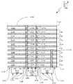
이 예에서, T/R 모듈(904)은, T/R 모듈(904)이 스위칭 가능한 송신 신호 경로 및 수신 신호 경로를 갖는 것을 가능하게 하는 회로를 포함할 수 있다. T/R 모듈(904)은 제1, 제2, 제3, 및 제4 송신 경로 스위치들(920, 922, 924, 및 926), 제1 및 제2 1:2 스플리터들(928 및 930), 제1 및 제2 로우 패스 필터들("LPF(low pass filter)들")(932 및 934), 제1 및 제2 하이 패스 필터들("HPF(high pass filter)들")(936 및 938), 제1, 제2, 제3, 및 제4, 제5, 제6, 및 제7 증폭기들(940, 942, 944, 946, 948, 950, 및 952), 위상-시프터(954), 및 감쇠기(956)를 포함할 수 있다.In this example, the T/
이 예에서, 제1 및 제2 송신 경로 스위치들(920 및 922)은 신호 경로(958)를 통해 MLPWB(902)의 RF 분배 네트워크(912)와 신호 통신할 수 있다. 부가하여, 제3 및 제4 송신 경로 스위치들(924 및 926)은 각각 신호 경로들(960 및 962)을 통해 MLPWB(902)의 방사 소자(906)와 신호 통신할 수 있다.In this example, first and second transmit path switches 920 and 922 can be in signal communication with the RF distribution network 912 of
또한, 제3 송신 경로 스위치(924) 및 제4 증폭기(946)는 제1 전력 스위칭 MMIC(914)의 일부일 수 있고, 제4 송신 경로 스위치(926) 및 제5 증폭기(948)는 제2 전력 스위칭 MMIC(916)의 일부일 수 있다. 제1 및 제2 전력 스위칭 MMIC들(914 및 916)이 전력 제공 IC들이기 때문에, 이들은 갈륨-비소("GaAs(gallium-arsenide)") 기술들을 활용하여 제작될 수 있다. 나머지 제1 및 제2 송신 경로 스위치들(920 및 922), 제1 및 제2 1:2 스플리터들(928 및 930), 제1 및 제2 LPF들(932 및 934), 제1 및 제2 HPF들(936 및 938), 제1, 제2, 제3, 제6, 및 제7 증폭기들(940, 942, 944, 950, 및 952), 위상-시프터(954), 및 감쇠기(956)는 빔 프로세싱 MMIC(918)의 일부일 수 있다. 빔 프로세싱 MMIC(918)는 실리콘-게르마늄("SiGe(silicon-germanium)") 기술들을 활용하여 제작될 수 있다. 이 예에서, SiGe 기술의 회로 기능들의 고밀도 및 고주파수 성능은, T/R 모듈의 회로 기능들의 풋프린트가 평면 타일 구성을 갖는 위상 어레이 안테나로 구현되도록 허용한다(즉, 일반적으로, 평면 모듈 회로 레이아웃 풋프린트는, 동작 주파수 및 최소 안테나 빔 스캔 요건으로 인해, 방사기 간격에 의해 제한됨).Also, the third transmit path switch 924 and the
도 10에서는, T/R 모듈(904)의 동작 예를 더욱 잘 이해시키기 위해, T/R 모듈(904)의 시스템 블록도가 도시된다. 동작 예에서는, 송신 모드에서, T/R 모듈(904)은 RF 분배 네트워크(912)로부터 신호 경로(1002)를 통해 입력 신호(1000)를 수신한다. 송신 모드에서, 제1 및 제2 송신 경로 스위치들(920 및 922)은, 송신 경로를 따라서 이 입력 신호(1000)를 전달하도록 설정되고, 이 송신 경로는 제1 송신 경로 스위치(920), 가변 감쇠기(956), 위상-시프터(954), 제1 증폭기(940), 및 제2 송신 경로 스위치(922)를 제1 1:2 스플리터(928)로 잇는 것을 포함한다. 이후, 결과적인 프로세싱된 입력 신호(1004)는 제1 1:2 스플리터(928)에 의해 두 개의 신호들(1006 및 1008)로 분할된다. 제1 분할 입력 신호(1006)는 제1 LPF(932)를 통해 전달되고, 제2 및 제4 증폭기들(942 및 946) 둘 다에 의해 증폭된다. 결과적인 증폭된 제1 분할 입력 신호(1010)는 제3 송신 경로 스위치(924)를 통해 방사 소자(906)의 제1 방사기(미도시)로 전달된다. 이 예에서, 제1 방사기는 제1 편파, 이를테면, 예컨대, 수직 편파 또는 오른손방향 원형 편파를 송신하도록 설정되는 방사기일 수 있다. 유사하게, 제2 분할 입력 신호(1008)는 제1 HPF(936)를 통해 전달되고, 제3 및 제5 증폭기들(944 및 948) 둘 다에 의해 증폭된다. 결과적인 증폭된 제2 분할 입력 신호(1012)는 제4 송신 경로 스위치(926)를 통해 방사 소자(906)의 제2 방사기(미도시)로 전달된다. 이 예에서, 제2 방사기는 제2 편파, 이를테면, 예컨대, 수평 편파 또는 왼손방향 원형 편파를 송신하도록 설정되는 방사기일 수 있다.In FIG. 10, a system block diagram of the T/
수신(리셉션으로서 또한 알려져 있음) 모드에서, T/R 모듈(904)은 방사 소자(906)의 제1 방사기로부터 제1 편파 수신 신호(1014)를 수신하고, 방사 소자(906)의 제2 방사기로부터 제2 편파 수신 신호(1016)를 수신한다.In receive (also known as reception) mode, the T/
수신 모드에서, 제1, 제2, 제3, 및 제4 송신 경로 스위치들(920, 922, 924, 및 926)은 제1 편파 수신 신호(1014) 및 제2 편파 수신 신호(1016)를 가변 감쇠기(956), 위상-시프터(954), 및 제1 증폭기(940)를 통해 RF 분배 네트워크(912)에 전달하도록 설정된다. 구체적으로, 제1 편파 수신 신호(1014)는 제3 송신 경로 스위치(924)를 통해 제6 증폭기(950)에 전달된다. 이후, 결과적인 증폭된 제1 편파 수신 신호(1018)는 제2 LPF(934)를 통해 제2 1:2 스플리터(930)에 전달되고, 이 제2 LPF(934)는 필터링된 제1 편파 수신 신호(1020)를 야기한다.In the receive mode, the first, second, third, and fourth transmit path switches 920, 922, 924, and 926 vary the first polarization received
유사하게, 제2 편파 수신 신호(1016)는 제4 송신 경로 스위치(926)를 통해 제7 증폭기(952)에 전달된다. 이후, 결과적인 증폭된 제2 편파 수신 신호(1022)는 제2 LPF(934)를 통해 제2 1:2 스플리터(930)에 전달되고, 이 제2 LPF(934)는 필터링된 제2 편파 수신 신호(1024)를 야기한다. 이후, 제2 1:2 스플리터(930)는 2:1 결합기로서 동작하고, 필터링된 제1 편파 수신 신호(1020) 및 필터링된 제2 편파 수신 신호(1024)를 결합시켜 결합 수신 신호(1026)를 생성하며, 이 결합 수신 신호(1026)가 제2 송신 경로 스위치(922), 가변 감쇠기(956), 위상-시프터(954), 제1 증폭기(940), 및 제1 송신 경로 스위치(920)를 통해 전달되어, 결합 수신 신호(1028)가 생성되고, 이 결합 수신 신호(1028)는 신호 경로(1002)를 통해 RF 분배 네트워크(912)에 전달된다.Similarly, the second polarization received
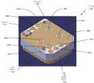
도 11을 참조하면, 본 발명에 따라, 하우징(1100)의 오픈 구현 예의 예상도가 도시된다. 이 예에서, 하우징(1100)은 허니콤 어퍼처 플레이트(1102) 및 압력 플레이트(1104)를 포함한다. 허니콤 어퍼처 플레이트(1102)는 이 허니콤 어퍼처 플레이트(1102)를 통과하는 복수의 채널들(1106)을 갖는 것으로 도시된다. 부가하여, 압력 플레이트(1104)는 복수의 T/R 모듈들(미도시)을 수용하기 위한 복수의 포켓들(1108)을 포함한다. 이 예에서, MLPWB(1110)는, 허니콤 어퍼처 플레이트(1102)와 압력 플레이트(1104) 사이에서 하우징(1100)의 내부에 들어맞는 구성으로 도시된다. 또한, MLPWB(1110)는 이 MLPWB(1110)의 하단 표면(1114)을 따라서 복수의 콘택들(1112)을 갖는 것으로 도시된다. 이 복수의 콘택들(1112)은, 일단 하우징(1100)에 배치되면, 복수의 T/R 모듈들(미도시)과 전기적으로 인터페이싱하도록 구성된다. 또한, RF 커넥터(도시되지 않았지만, 도 4 및 도 5에 설명됨) 및 다른 전기 연결들(이를테면, 예컨대, 바이어싱, 접지, 전원 등)과 RF 분배 네트워크(도시되지 않았고, MLPWB(1110)의 층들 내에 있음)를 인터페이싱시키기 위한 부가적인 콘택들(1116)이 도시된다.Referring to FIG. 11 , a projected view of an example of an open implementation of a
도 12에서는, 도 11에 설명된 오픈 하우징(1100)의 다른 예상도가 도시된다. 이 예에서, MLPWB(1110)는 압력 플레이트(1104)의 내부 표면(1200)에 맞닿게 배치된 것으로 도시된다. 이 도면에서, MLPWB(1110)의 상단 표면(1204)에 형성된 복수의 방사 소자들(1202)이 도시된다. 도 13에서는, WAIM 시트가 허니콤 어퍼처 플레이트(1102)의 위에 설치되지 않은 클로즈드 하우징(1100)의 예상 평면도가 도시된다. 복수의 채널들(1106)을 포함하는 허니콤 어퍼처 플레이트(1102)가 도시된다. 도 14를 참조하면, 허니콤 어퍼처 플레이트(1102)의 위에 설치된 WAIM 시트(1400)를 갖는 클로즈드 하우징(1100)의 예상 평면도가 도시된다. 또한, 하우징(1100)의 하단은 예시적 RF 커넥터(1402)를 갖는 것으로 도시된다.In FIG. 12, another prospective view of the
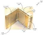
도 15를 참조하면, 본 발명에 따라, 하우징(1500)의 구현 예의 분해된 예상 저면도가 도시된다. 이 예에서, 하우징(1500)은 하단 면(1504)을 갖는 압력 플레이트(1502), 허니콤 어퍼처 플레이트(1506), 와이어링 공간(1508), 와이어링 공간 커버(1510), 및 RF 커넥터(1512)를 포함한다. 하우징(1500)의 내부에는 MLPWB(1514), 제1 스페이서(1516), 제2 스페이서(1518), 및 전력 하니스(1520)가 있다. 전력 하니스(1520)는 전력을 STRPAA에 제공하고, 버스 타입 신호 경로를 포함할 수 있으며, 이 전력 하니스(1520)는 도 1에 도시된 전원(108), 제어기(104), 및 온도 제어 시스템(106)과 신호 통신할 수 있다. 전력 하니스(1520)는 와이어링 공간(1508) 내에 위치되고, MLPWB 인터페이스 커넥터 또는 커넥터들(1522)을 통해 MLPWB(1514)와 신호 통신할 수 있고 그리고 하우징 커넥터(1524)를 통해 도 1의 전원(108), 제어기(104), 및 온도 제어 시스템(106)과 신호 통신할 수 있다. 다시, 허니콤 어퍼처 플레이트(1506)는 복수의 채널들(1526)을 포함한다.Referring to FIG. 15 , an exploded, projected bottom view of an embodiment of a housing 1500, in accordance with the present invention, is shown. In this example, a housing 1500 includes a
이 예에서, 스페이서들(1516 및 1518)은 MLWPB(1514) 접지 평면들과 인접한 금속 플레이트들(즉, 각각, 압력 플레이트(1502)와 허니콤 어퍼처 플레이트(1506)) 사이에 접지 연결들을 제공하기 위해 패터닝된 범프들을 갖는 전도성 시트들(즉, 예컨대, 금속)이다. 구체적으로, 스페이서(1516)는 MLPWB(1514)와 압력 플레이트(1502) 사이에서 RF 접지를 유지시킨다. 스페이서(1518)는 MLPWB(1514)와 허니콤 어퍼처 플레이트(1506) 사이에서 RF 접지를 유지시킨다. 또한, 이러한 RF 접지 및 격리 없이, 발생할 수 있는 성능 저하를 방지하기 위해, 스페이서들(1516 및 1518)의 형상 및 컷아웃 패턴이 개별 어레이 소자들 사이에서 RF 격리를 유지시킨다. 일반적으로, 스페이서들(1516 및 1518)은, 섀시 컴포넌트들(예컨대, 압력 플레이트(1502) 및 허니콤 어퍼처 플레이트(1506))와 MLPWB(1514) 사이에 존재하는 임의의 편평도 불규칙성들을 흡수함으로써, 접지 및 격리를 유지시킨다. 이 능력은 추가로, 편평도 불규칙성들을 흡수하기 위해 압축될 때 다양한 정도들로 붕괴될 수 있는 마이크로 범프들을 복수의 심(shim)들(즉, 스페이서들(1516 및 1518))의 표면에서 활용함으로써 개선될 수 있다.In this example,
도 16에서는, 본 발명에 따라, 압력 플레이트(1614)의 내부 표면(1612)을 따라서 있는 포켓들(1600, 1602, 1604, 1604, 1606, 1608, 및 1610)(도 11에서는 포켓들(1108)로서 설명됨)의 구현 예의 평면도가 도시된다. 이 예에서, 제1 및 제2 포켓들(1600 및 1602)은 각각 제1 및 제2 압축 스프링(1616 및 1618)을 포함한다. 제1 및 제2 포켓들(1600 및 1602) 안으로 그리고 제1 및 제2 압축 스프링(1616 및 1618)에 맞닿게, 제1 및 제2 T/R 모듈들(1620 및 1622)이 각각 배치된다. 이 예에서, 포켓들의 압축 스프링들은 T/R 모듈들을 MLPWB의 하단 표면에 맞닿게 밀어내기 위해 이 T/R 모듈들의 하단에 압축력을 제공한다. 도 4 및 도 5에 설명된 예들과 유사하게, 각각의 T/R 모듈(1620 및 1622)은 각각 홀더(1624 및 1626)를 포함하고, 이 홀더(1624 및 1626)는 각각 복수의 전기 인터커넥트 신호 콘택들(1628 및 1630)을 포함한다.In FIG. 16 , pockets 1600, 1602, 1604, 1604, 1606, 1608, and 1610 along
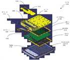
도 17을 참조하면, 본 발명에 따라, 복수의 전기 인터커넥트 신호 콘택들(1702)과 결합되는 T/R 모듈(1700)의 구현 예의 분해된 사시 측면도가 도시된다. 전기 인터커넥트 신호 콘택들(1702)(이 예에서는, fuzz buttons®로서 도시됨)은 상단 표면(1706) 및 하단 표면(1708)을 갖는 홀더(1704) 내에 위치된다. T/R 모듈(1700)은 상단 표면(1710) 및 하단 표면(1712)을 포함하는데, 여기서 그들은 상단 표면(1710) 상에 위치된 커패시터(1714) 및 하단 표면(1712) 상에 위치된 RF 모듈(1716)일 수 있다. 대안적 구현에서, 홀더(1704)는 존재하지 않을 것이고, 전기 인터커넥트 신호 콘택들(1702)은 복수의 솔더 볼들, 즉, 볼 그리드일 수 있다.Referring to FIG. 17 , an exploded perspective side view of an example implementation of a T/R module 1700 coupled with a plurality of electrical
도 18에서는, 본 발명에 따라, 평면 회로 T/R 모듈(1700)(본원에서, 일반적으로, T/R 모듈로 지칭됨)의 분해된 사시 평면도가 도시된다. 구체적으로, RF 모듈(1716)이 RF 모듈 리드(lid)(1800), 제1 전력 스위칭 MMIC(1802), 제2 전력 스위칭 MMIC(1804), 빔 프로세싱 MMIC(1806), 모듈 캐리어(1808), 및 T/R 모듈 세라믹 패키지(1810)를 포함함을 나타내기 위해, RF 모듈(1716)이 분해된다. 이 예에서, T/R 모듈 세라믹 패키지(1810)는 T/R 모듈(1700)의 상단 표면(1710)에 대응하는 상단 표면 및 하단 표면(1812)을 갖는다. T/R 모듈 세라믹 패키지(1810)의 하단 표면(1812)은, 제1 전력 스위칭 MMIC(1802), 제2 전력 스위칭 MMIC(1804), 및 빔 프로세싱 MMIC(1806)가 T/R 모듈 세라믹 패키지(1810)와 신호 통신하도록 허용하기 위하여 신호 경로들을 형성하는 복수의 T/R 모듈 콘택들(1814)을 포함한다. 이 예에서, 제1 전력 스위칭 MMIC(1802), 제2 전력 스위칭 MMIC(1804), 및 빔 프로세싱 MMIC(1806)는 모듈 캐리어(1808) 내에 배치되고 RF 모듈 리드(1800)에 의해 커버된다. 이 예에서, 제1 전력 스위칭 MMIC(1802), 제2 전력 스위칭 MMIC(1804), 및 빔 프로세싱 MMIC(1806)는 모듈 캐리어(1808)에서 플립-칩 구성으로 배치될 수 있는데, 여기서 제1 전력 스위칭 MMIC(1802) 및 제2 전력 스위칭 MMIC(1804)는 그들의 칩 콘택들이 하단 표면(1812)으로부터 멀리 향하도록 지향될 수 있고 빔 프로세싱 MMIC(1806)는 제1 전력 스위칭 MMIC(1802) 및 제2 전력 스위칭 MMIC(1804)의 반대 방향으로 있을 수 있다.In Fig. 18, an exploded perspective plan view of a planar circuit T/R module 1700 (herein generally referred to as a T/R module) is shown, in accordance with the present invention. Specifically, the RF module 1716 includes an
MLPWB와 유사하게, STRPAA의 하우징의 경우, T/R 모듈 세라믹 패키지(1810)가, 신호들이 T/R 모듈 콘택들(1814)로부터 T/R 모듈(1700)의 상단 표면(1710) 상의 T/R 모듈 상단 표면 콘택들(미도시)로 전달되도록 허용하는, 다수의 층들의 기판 및 금속 형성 마이크로회로들을 포함할 수 있음이 당업자들에 의해 인식된다. 예로서, T/R 모듈 세라믹 패키지(1810)는 다수의 비아들과 함께 대략 0.005 인치의 기판 두께를 갖는 열 한(11) 개의 층들의 금속성 재료(이를테면, 예컨대, 금 금속화부를 갖는 질화알루미늄("AlN(aluminum nitride)" 기판)와 열(10) 개의 층들의 세라믹 기판을 포함할 수 있다.Similar to the MLPWB, in the case of the STRPAA's housing, the T/R module ceramic package 1810 allows signals to pass from the T/
도 19에서는, 본 발명에 따라, 모듈 캐리어(1808)에 설치된 제1 전력 스위칭 MMIC(1802), 제2 전력 스위칭 MMIC(1804), 및 빔 프로세싱 MMIC(1806)를 갖는 (타일 구성의) T/R 모듈(1700)의 사시 평면도가 도시된다.19 shows a T/T (in tiled configuration) with a first
도 20을 참조하면, 본 발명에 따라, T/R 모듈(1700)의 사시 저면도가 도시된다. 이 예에서, T/R 모듈(1700)의 상단 표면(1710)은 전기 인터커넥트 신호 콘택들과 신호 통신하는 다수의 전도성 금속성 패드들(2000, 2002, 2004, 2004, 2006, 2008, 2010, 2012, 2014, 및 2016)을 포함할 수 있다. 이 예에서, 제1 전도성 금속성 패드(2000)는 공통 접지 평면일 수 있다. 제2 전도성 금속성 패드(2002)는 제1 RF 신호를 생성할 수 있고, 이 제1 RF 신호는 T/R 모듈(1700)에 대응하는 방사 소자 상의 제1 방사기(미도시)의 제1 프로브에 입력된다. 이 예에서, T/R 모듈(1700)로부터 제2 전도성 금속성 패드(2002)를 통해 출력되는 신호는, 제1 편파를 갖는 방사선을 생성하기 위해 대응하는 방사 소자에 의해 활용될 수 있다. 유사하게, 제3 전도성 금속성 패드(2004)는 제2 RF 신호를 생성할 수 있고, 이 제2 RF 신호는 대응하는 방사 소자 상의 제2 방사기(미도시)의 제2 프로브에 입력된다. T/R 모듈(1700)로부터 제3 전도성 금속성 패드(2004)를 통해 출력되는 신호는, 제1 편파에 직교하는 제2 편파를 갖는 방사선을 생성하기 위해 대응하는 방사 소자에 의해 활용될 수 있다.Referring to Fig. 20, a perspective bottom view of a T/R module 1700 is shown, in accordance with the present invention. In this example, the
제4 전도성 금속성 패드(2006)는 RF 통신 포트일 수 있다. 제4 전도성 금속성 패드(2006)는 RF 공통 포트일 수 있고, 이 RF 공통 포트는 송신 모드에서는 T/R 모듈(1700)에 대한 입력 RF 포트이고 수신 모드에서는 T/R 모듈(1700)에 대한 출력 RF 포트이다. 다시 도 9를 참조하면, 제4 전도성 금속성 패드(2006)는 RF 분배 네트워크(912)와 신호 통신한다. 제5 전도성 금속성 패드(2008)는 직류("DC(direct current)") 신호(이를테면, 예컨대, +5 볼트 신호)를 생성하는 포트일 수 있고, 이 신호는 제1 전도성 금속성 패드(2008)를, 0 볼트와 동일할 수 있는 접지 값으로 설정하거나 또는 다른 기준 DC 전압 레벨, 이를테면, 예컨대, 제5 전도성 금속성 패드(2008)에 의해 공급되는 +5 볼트로 설정한다. 커패시터(1714)는 제5 전도성 금속성 패드(2008)와 신호 통신하는 MMIC들(즉, MIMIC들(1802 및 1804))에 안정성을 제공한다.The fourth conductive
부가하여, 이 예에서, 포트(2008)는 전력 스위칭 MMIC들(1802 및 1804)의 GaAs 전력 증폭기에 +5V 바이어싱 전압을 제공하고, 포트들(2010 및 2016)은 SiGe 빔 프로세싱 MMIC(1806), 및 GaAs 전력 스위칭 MMIC(1802 및 1804)에 -5V 바이어싱 전압을 제공한다. 포트(2012)는 디지털 데이터 신호를 제공하고, 포트(2018)는 디지털 클록 신호를 제공하며, 이들 신호들 둘 다는 SiGe 빔 프로세싱 MMIC(1806)의 위상 시프터들에 대한 것이고, 어레이 빔 스티어링 제어의 일부를 형성한다. 또한, 포트(2014)는 SiGe MMIC(1806)에 +3.3V 바이어싱 전압을 제공한다.Additionally, in this example,
이 예에서, T/R 모듈 세라믹 패키지(1810)는, 신호들이 T/R 모듈 콘택들(1814)로부터 T/R 모듈(1700)의 상단 표면(1710) 상의 T/R 모듈 상단 표면 콘택들(미도시)로 전달되도록 허용하는, 다수의 층들의 기판 및 금속 형성 마이크로회로들을 포함할 수 있다.In this example, the T/R module ceramic package 1810 allows signals to pass from the T/
도 21을 참조하면 그리고 도 3과 유사하게, 본 발명에 따라, T/R 모듈 세라믹 패키지(2100)(T/R 모듈 세라믹 패키지(2100)로서 또한 알려져 있음)의 구현 예의 부분적 단면도가 도시된다. 이 예에서, T/R 모듈 세라믹 패키지(2100)는 열(10) 개의 기판 층들(2102, 2104, 2106, 2108, 2110, 2112, 2114, 2116, 2118, 및 2120) 및 열 한(11) 개의 금속성 층들(2122, 2124, 2126, 2128, 2130, 2132, 2134, 2136, 2138, 2140, 및 2142)을 포함할 수 있다. 이 예에서, 빔 프로세싱 MMIC(1806) 및 전력 스위칭 MMIC들(1802 및 1804)은 T/R 모듈 세라믹 패키지(2100)의 하단 표면(2144)에 플립-칩 구성으로 위치된다. 이 예에서, 빔 프로세싱 MMIC(1806)의 하단으로부터 T/R 모듈 세라믹 패키지(2100)의 하단 표면(2144)의 방향으로 돌출하는 솔더 범프들(2146)을 갖는 빔 프로세싱 MMIC(1806)가 도시된다. 빔 프로세싱 MMIC(1806) 솔더 범프들(2146)은, T/R 모듈 세라믹 패키지(2100)의 하단 표면(2144)으로부터 빔 프로세싱 MMIC(1806)의 방향으로 돌출하는, T/R 모듈 세라믹 패키지(2100)의 솔더 범프들(2146)과 신호 통신한다. 유사하게, 전력 스위칭 MMIC들(1802 및 1804)은 또한, 각각 솔더 범프들(2150 및 2152)을 갖고, 이 솔더 범프들(2150 및 2152)은 각각 T/R 모듈 세라믹 패키지(2100)의 하단 표면(2144)의 솔더 범프들(2152, 2154, 2156, 및 2158)과 신호 통신한다. 도 3에 도시된 MLPWB(300)와 유사하게, T/R 모듈 세라믹 패키지(2100)는 복수의 비아들(2159, 2160, 2161, 2162, 2163, 2164, 2165, 2166, 2167, 2168, 2169, 2170, 2171, 2172, 2173, 2174, 2175, 2176, 2177, 2178, 및 2179)을 포함할 수 있다. 이 예에서, 비아(2179)는 하단 표면(2144)으로부터, T/R 모듈 세라믹 패키지(2100)의 하단 표면(2144)과 상단 표면(2180) 사이의 내부 기판 층(2104, 2106, 2108, 2110, 2112, 2114, 2116, 및 2118)으로 이어지는 블라인드 홀일 수 있다. 도 3에 도시된 기판 층들과 유사하게, 각각의 개별적인 기판 층(2102, 2104, 2106, 2108, 2110, 2112, 2114, 2116, 2118, 및 2120)이 각각의 기판 층 내에 에칭된 회로를 포함할 수 있음이 당업자들에 의해 인식된다.Referring to FIG. 21 and similarly to FIG. 3 , a partial cross-sectional view of an example implementation of a T/R module ceramic package 2100 (also known as a T/R module ceramic package 2100) is shown, in accordance with the present invention. In this example, a T/R
도 22에서는, T/R 모듈 세라믹 패키지(2204)의 하단 표면(2202) 상에서의 인쇄 와이어링 어셈블리(2200)의 구현 예의 도면이 도시된다. 인쇄 와이어링 어셈블리(2200)는, 빔 프로세싱 MMIC(1806) 및 전력 스위칭 MMIC들(1802 및 1804)의 솔더 범프들 또는 스터드 범프들(도 21에 도시됨)에 본딩될 솔더 또는 골드 스터드 범프들(2205, 2206, 2208, 2210, 2212, 2214, 2216, 2218, 2220, 2222, 2224, 2226, 2228, 2230, 2232, 2234, 2236, 2238, 2240, 및 2242)을 갖는 복수의 전기 패드들을 포함한다.In FIG. 22 , a diagram of an example implementation of a printed
도 23을 참조하면, 본 발명에 따라, 도 22에 도시된 인쇄 와이어링 어셈블리(2200) 상에 빔 프로세싱 MMIC(1806) 및 전력 스위칭 MMIC들(1802 및 1804)의 장착의 구현 예를 예시하는 도면이 도시된다. 이 예에서, 레이아웃은 타일 구성이다. 부가하여, 이 예에서, 빔 프로세싱 MMIC(1806) 및 전력 스위칭 MMIC들(1802 및 1804) 그리고 인쇄 와이어링 어셈블리(2200) 전기 패드들(2205, 2206, 2208, 2210, 2212, 2214, 2216, 2218, 2220, 2222, 2224, 2226, 2228, 2230, 2232, 2234, 2236, 2238, 2240, 및 2242) 사이에 와이어 본드 연결들(2300, 2302, 2304, 2306, 2308, 및 2310)이 도시된다. 구체적으로, 와이어 본드들(2300, 2310, 및 2308)을 통해 각각 전기 패드들(2205, 2206, 2234, 2236, 2238, 및 2242)과 신호 통신하는 제1 전력 스위칭 MMIC(1802)가 도시된다. 유사하게, 와이어 본드들(2302, 2304, 및 2306)을 통해 각각 전기 패드들(2214, 2216, 2218, 2222, 2224, 및 2226)과 신호 통신하는 제2 전력 스위칭 MMIC(1804)가 도시된다. 솔더 범프들(도 21에 도시됨)을 통해 전기 패드들(2206, 2209, 2210, 2212, 2214, 2218, 2220, 2226, 2228, 2230, 2232, 2234, 2240, 및 2242)과 신호 통신하는 빔 프로세싱 MMIC(1806)가 도시된다.Referring to FIG. 23, a diagram illustrating an example implementation of mounting of a
추가로, 본 개시물은 하기의 경우들에 따른 실시예들을 포함한다:Additionally, the present disclosure includes embodiments according to the following cases:
경우 1. 스위칭 가능한 송수신 페이즈드 어레이 안테나("STRPAA")로서, 상기 STRPAA는:
하우징;housing;
상기 하우징 내의 다층 인쇄 와이어링 보드("MLPWB") ― 상기 MLPWB는,A multi-layer printed wiring board ("MLPWB") in the housing - the MLPWB comprising:
상단 표면, 및top surface, and
하단 표면을 가짐―;has a lower surface;
상기 MLPWB의 상기 상단 표면 상에 위치된 복수의 방사 소자들; 및a plurality of radiating elements positioned on the top surface of the MLPWB; and
상기 MLPWB의 상기 하단 표면에 부착된 복수의 송수신("T/R") 모듈들A plurality of transmit/receive (“T/R”) modules attached to the bottom surface of the MLPWB
을 포함하고,including,
상기 복수의 T/R 모듈들은 상기 MLPWB의 상기 하단 표면과 신호 통신하고,the plurality of T/R modules are in signal communication with the bottom surface of the MLPWB;
상기 복수의 T/R 모듈들의 각각의 T/R 모듈은, 상기 MLPWB의 상기 상단 표면 상에 위치된 상기 복수의 방사 소자들 중 대응하는 방사 소자에 대향하게 상기 MLPWB의 상기 하단 표면 상에 위치되고, 그리고each T/R module of the plurality of T/R modules is positioned on the bottom surface of the MLPWB opposite a corresponding one of the plurality of radiating elements positioned on the top surface of the MLPWB; , and
각각의 T/R 모듈은 T/R 모듈에 대향하게 위치된 대응하는 방사 소자와 신호 통신한다.Each T/R module is in signal communication with a corresponding radiating element positioned opposite the T/R module.
경우 2. 경우 1의 STRPAA로서, 상기 하우징은,
압력 플레이트, 및a pressure plate; and
복수의 채널들을 갖는 허니콤 어퍼처 플레이트Honeycomb Aperture Plate with Multiple Channels
를 포함하고,including,
상기 압력 플레이트는 상기 MLPWB의 상기 하단 표면에 맞닿게 상기 복수의 T/R 모듈들을 밀어내도록 구성되고,the pressure plate is configured to push the plurality of T/R modules into contact with the bottom surface of the MLPWB;
상기 복수의 방사 소자들은 상기 허니콤 어퍼처 플레이트에 거의 맞닿게 배치되도록 구성되며, 그리고The plurality of radiating elements are configured to be disposed substantially in contact with the honeycomb aperture plate, and
상기 복수의 방사 소자들의 각각의 방사 소자는 상기 허니콤 어퍼처의 상기 복수의 채널들 중 대응하는 채널에 위치된다.Each radiating element of the plurality of radiating elements is located in a corresponding one of the plurality of channels of the honeycomb aperture.
경우 3. 경우 2의 STRPAA로서, 상기 허니콤 어퍼처 플레이트와 신호 통신하는 광각 임피던스 매칭("WAIM") 시트Case 3. The STRPAA of
를 더 포함한다.more includes
경우 4. 경우 3의 STRPAA로서, 상기 복수의 방사 소자들의 각각의 방사 소자는 인쇄 안테나이다.Case 4. STRPAA of case 3, wherein each radiating element of the plurality of radiating elements is a printed antenna.
경우 5. 경우 2의 STRPAA로서, 각각의 T/R 모듈은 복수의 고성능 신호 콘택들을 통해 상기 MLPWB의 상기 하단 표면과 신호 통신하게 배치된다.Case 5. The STRPAA of
경우 6. 경우 5의 STRPAA로서, 각각의 T/R 모듈은 적어도 세 개의 모놀리식 마이크로파 집적 회로들("MMIC들")을 포함한다.Case 6. The STRPAA of case 5, wherein each T/R module includes at least three monolithic microwave integrated circuits (“MMICs”).
경우 7. 경우 6의 STRPAA로서, 적어도 세 개의 MMIC들 중 제1 MMIC는 빔 프로세싱 MMIC이고, 제2 및 제3 MMIC들은 전력 스위칭 MMIC들이다.Case 7. STRPAA of case 6, wherein a first MMIC of the at least three MMICs is a beam processing MMIC, and second and third MMICs are power switching MMICs.
경우 8. 경우 7의 STRPAA로서, 상기 제1 MMIC는 실리콘-게르마늄("SiGe") 기술들을 활용하고, 상기 제2 및 제3 MMIC들은 갈륨-비소("GaAs") 기술들을 활용한다.Case 8. The STRPAA of case 7, wherein the first MMIC utilizes silicon-germanium ("SiGe") technologies and the second and third MMICs utilize gallium-arsenide ("GaAs") technologies.
경우 9. 경우 7의 STRPAA로서, 적어도 하나의 MMIC는 물리적으로 플립-칩 구성으로 구성된다.Case 9. STRPAA of case 7, wherein at least one MMIC is physically configured in a flip-chip configuration.
경우 10. 경우 2의 STRPAA로서,Case 10. As STRPAA in
복수의 비아들multiple vials
을 더 포함하고,Including more,
상기 복수의 비아들의 각각의 비아는 상기 MLPWB를 통과하고, 그리고 상기 MLPWB의 상기 하단 표면 상의 상기 복수의 T/R 모듈들의 T/R 모듈과, 상기 MLPWB의 상기 상단 표면 상에 위치된 상기 복수의 방사 소자들 중 상기 T/R 모듈에 대향하는 방사 소자 사이의 신호 경로로서 구성된다.Each via of the plurality of vias passes through the MLPWB, and a T/R module of the plurality of T/R modules on the bottom surface of the MLPWB and the plurality of T/R modules located on the top surface of the MLPWB Among the radiating elements, it is configured as a signal path between radiating elements facing the T/R module.
경우 11. 경우 10의 STRPAA로서,Case 11. As STRPAA in Case 10,
상기 MLPWB는 두 개의 인쇄 와이어 보드("PWB") 서브-어셈블리들을 포함한다.The MLPWB includes two printed wire board ("PWB") sub-assemblies.
경우 12. 경우 11의 STRPAA로서,Case 12. As STRPAA in Case 11,
상기 두 개의 PWB 서브-어셈블리들은 본딩 재료를 갖는 본딩 층에 의해 서로 본딩되고, 상기 본딩 재료는 상기 두 개의 PWB 서브-어셈블리들 사이에서 기계적 및 전기적 연결 둘 다를 형성한다.The two PWB sub-assemblies are bonded to each other by a bonding layer having a bonding material, and the bonding material forms both a mechanical and electrical connection between the two PWB sub-assemblies.
경우 13. 경우 12의 STRPAA로서, 각각의 PWB 서브-어셈블리는 대응하는 복수의 금속성 층들을 갖는 복수의 기판들을 포함한다.Case 13. The STRPAA of case 12, wherein each PWB sub-assembly includes a plurality of substrates having a corresponding plurality of metallic layers.
경우 14. 경우 8의 STRPAA로서, 각각의 T/R 모듈은, 대응하는 복수의 금속성 층들을 갖는 복수의 세라믹 기판들을 포함하는 T/R 모듈 세라믹 패키지를 포함한다.Case 14. The STRPAA of case 8, wherein each T/R module includes a T/R module ceramic package including a plurality of ceramic substrates having a corresponding plurality of metallic layers.
경우 15. 경우 14의 STRPAA로서, 상기 T/R 모듈 세라믹 패키지는 상기 복수의 고성능 신호 콘택들과 신호 통신하는 상단 표면 및 상기 적어도 세 개의 MMIC들과 신호 통신하는 하단 표면을 포함한다.Case 15. The STRPAA of case 14, wherein the T/R module ceramic package includes a top surface in signal communication with the plurality of high performance signal contacts and a bottom surface in signal communication with the at least three MMICs.
경우 16. 경우 15의 STRPAA로서,
복수의 비아들multiple vials
을 더 포함하고,Including more,
상기 복수의 비아들의 각각의 비아는 상기 T/R 모듈 세라믹 패키지를 통과하고, 그리고 상기 T/R 모듈 세라믹 패키지의 상기 하단 표면 상의 상기 적어도 세 개의 MMIC들의 MMIC와, 상기 T/R 모듈 세라믹 패키지의 상기 상단 표면 상에 위치된, 상기 MMIC에 대향하는 전도성 금속성 패드 사이의 신호 경로로서 구성된다.Each via of the plurality of vias passes through the T/R module ceramic package, and the MMIC of the at least three MMICs on the bottom surface of the T/R module ceramic package and the T/R module ceramic package It is configured as a signal path between conductive metallic pads located on the top surface, opposite the MMIC.
경우 17. 경우 1의 STRPAA로서, 상기 STRPAA는 K-대역에서 동작하도록 구성된다.Case 17. The STRPAA of
경우 18. 경우 1의 STRPAA로서, 상기 복수의 방사 소자들의 각각의 방사 소자는 각각의 대응하는 T/R 모듈에 대한 신호 어퍼처이다.Case 18. The STRPAA of
경우 19. 스위칭 가능한 송수신 페이즈드 어레이 안테나("STRPAA")에서 사용하기 위한 송수신("T/R") 모듈로서, 상기 T/R 모듈은,Case 19. A transmit/receive (“T/R”) module for use in a switchable transmit/receive phased array antenna (“STRPAA”), the T/R module comprising:
빔 프로세싱 모놀리식 마이크로파 집적 회로("MMIC");a beam processing monolithic microwave integrated circuit ("MMIC");
제1 및 제2 전력 스위칭 MMIC들;first and second power switching MMICs;
T/R 다층 인쇄 와이어링 보드(MLPWB) ― 상기 MLPWB는,T/R multi-layer printed wiring board (MLPWB) - the MLPWB includes:
대응하는 복수의 금속성 층들을 갖는 복수의 기판들,a plurality of substrates having a corresponding plurality of metallic layers;
상단 표면, top surface,
하단 표면(228), 및
복수의 비아들을 가짐―; having a plurality of vias;
를 포함하고,including,
빔 프로세싱 MMIC와 상기 제1 및 제2 전력 스위칭 MMIC들은, 물리적으로 T/R 모듈 세라믹 패키지의 하단 표면과 신호 통신하는 플립-칩 구성으로 구성되고,The beam processing MMIC and the first and second power switching MMICs are physically configured in a flip-chip configuration in signal communication with a bottom surface of a T/R module ceramic package,
상기 복수의 비아들의 각각의 비아는 상기 T/R 모듈 세라믹 패키지를 통과하고, 그리고 상기 T/R 모듈 세라믹 패키지의 상기 하단 표면 상의 상기 빔 프로세싱 MMIC와 제1 및 제2 전력 스위칭 MMIC들 중의 MMIC와, 상기 T/R 모듈 세라믹 패키지의 상기 상단 표면 상에 위치된, 상기 MMIC에 대향하는 전도성 금속성 패드 사이의 신호 경로로서 구성된다.Each via of the plurality of vias passes through the T/R module ceramic package, and the MMIC of the beam processing MMIC and first and second power switching MMICs on the bottom surface of the T/R module ceramic package , as a signal path between the conductive metallic pads opposite the MMIC, located on the top surface of the T/R module ceramic package.
경우 20. 경우 19의 T/R 모듈로서, 상기 STRPAA는 K-대역에서 동작하도록 구성된다.Case 20. The T/R module of case 19, wherein the STRPAA is configured to operate in K-band.
본 개시물의 범위로부터 벗어남 없이 본 개시물의 다양한 양상들 또는 세부사항들이 변경될 수 있음이 이해될 것이다. 본 개시물은 완전하지 않으며, 청구되는 개시물들을 개시된 정확한 형태로 제한하지 않는다. 또한, 전술된 설명은 예시 목적만을 위한 것이고, 제한 목적을 위한 것이 아니다. 수정들 및 변형들이 위의 설명을 고려하여 가능하거나, 또는 본 개시물을 실시하는 것으로부터 취득될 수 있다. 청구항들 및 그들의 등가물들이 본 개시물의 범위를 정의한다.It will be understood that various aspects or details of this disclosure may be changed without departing from its scope. This disclosure is not exhaustive and does not limit the claimed disclosure to the precise form disclosed. Also, the foregoing description is for illustrative purposes only and not for limiting purposes. Modifications and variations are possible in light of the above description, or may be acquired from practicing the present disclosure. The claims and their equivalents define the scope of this disclosure.
Claims (19)
Translated fromKorean압력 플레이트, 및 복수의 채널들을 갖는 허니콤 어퍼처 플레이트를 갖는 하우징;
상기 하우징 내의 다층 인쇄 와이어링 보드("MLPWB(multilayer printed wiring board)") ― 상기 MLPWB는, 상단 표면 및 하단 표면을 가짐 ―;
상기 MLPWB의 상기 상단 표면 상에 위치된 복수의 방사 소자들; 및
상기 MLPWB의 상기 하단 표면에 해제 가능하게(releasably) 부착되고, 상기 하우징이 닫힐 때 상기 압력 플레이트와 물리적으로 접촉하는 복수의 송수신("T/R(transmit and receive)") 모듈들을 포함하고,
상기 복수의 T/R 모듈들은 상기 MLPWB의 상기 하단 표면과 신호 통신하고,
상기 복수의 T/R 모듈들의 각각의 T/R 모듈은, 상기 MLPWB의 상기 상단 표면 상에 위치된 상기 복수의 방사 소자들 중 대응하는 방사 소자에 대향하게 상기 MLPWB의 상기 하단 표면 상에 위치되고,
각각의 T/R 모듈은 T/R 모듈에 대향하게 위치된 대응하는 방사 소자와 신호 통신하고,
상기 압력 플레이트는 상기 MLPWB의 상기 하단 표면에 맞닿게 상기 복수의 T/R 모듈들을 밀어내도록 구성되고,
상기 복수의 방사 소자들은, 상기 하우징이 닫힐 때 상기 허니콤 어퍼처 플레이트에 거의 맞닿게 배치되도록 구성되고,
상기 복수의 방사 소자들의 각각의 방사 소자는 상기 허니콤 어퍼처의 상기 복수의 채널들 중 대응하는 채널에 위치되며,
각각의 T/R 모듈은, 상기 하우징이 닫힐 때 상기 압력 플레이트에 의해 복수의 전기 인터커넥트 신호 콘택들을 통해 상기 MLPWB의 상기 하단 표면과 신호 통신하게 배치되는,
스위칭 가능한 송수신 페이즈드 어레이 안테나("STRPAA").As a switchable transmit and receive phased array antenna ("STRPAA (switchable transmit and receive phased array antenna)"),
a housing having a pressure plate and a honeycomb aperture plate having a plurality of channels;
a multilayer printed wiring board (“MLPWB”) within the housing, the MLPWB having a top surface and a bottom surface;
a plurality of radiating elements positioned on the top surface of the MLPWB; and
a plurality of transmit and receive (“T/R”) modules releasably attached to the bottom surface of the MLPWB and in physical contact with the pressure plate when the housing is closed;
the plurality of T/R modules are in signal communication with the bottom surface of the MLPWB;
each T/R module of the plurality of T/R modules is positioned on the bottom surface of the MLPWB opposite a corresponding one of the plurality of radiating elements positioned on the top surface of the MLPWB; ,
each T/R module is in signal communication with a corresponding radiating element positioned opposite the T/R module;
the pressure plate is configured to push the plurality of T/R modules into contact with the bottom surface of the MLPWB;
the plurality of radiating elements are configured to be disposed substantially in contact with the honeycomb aperture plate when the housing is closed;
Each radiating element of the plurality of radiating elements is located in a corresponding one of the plurality of channels of the honeycomb aperture;
each T/R module is placed in signal communication with the bottom surface of the MLPWB via a plurality of electrical interconnect signal contacts by the pressure plate when the housing is closed.
Switchable Transmit/Receive Phased Array Antenna (“STRPAA”).
각각의 T/R 모듈은 적어도 세 개의 모놀리식 마이크로파 집적 회로들("MMIC들(monolithic microwave integrated circuits)")을 포함하고,
제1 MMIC는 실리콘-게르마늄("SiGe") 기술들을 활용하고, 제2 및 제3 MMIC들은 갈륨-비소("GaAs") 기술들을 활용하는,
스위칭 가능한 송수신 페이즈드 어레이 안테나("STRPAA").According to claim 1,
Each T/R module includes at least three monolithic microwave integrated circuits (“monolithic microwave integrated circuits” (“MMICs”));
wherein the first MMIC utilizes silicon-germanium ("SiGe") technologies and the second and third MMICs utilize gallium-arsenic ("GaAs") technologies;
Switchable Transmit/Receive Phased Array Antenna (“STRPAA”).
상기 허니콤 어퍼처 플레이트와 신호 통신하는 광각 임피던스 매칭("WAIM(wide angle impedance matching)") 시트를 더 포함하는,
스위칭 가능한 송수신 페이즈드 어레이 안테나("STRPAA").According to claim 1,
Further comprising a wide angle impedance matching (“WAIM”) sheet in signal communication with the honeycomb aperture plate.
Switchable Transmit/Receive Phased Array Antenna (“STRPAA”).
상기 복수의 방사 소자들의 각각의 방사 소자는 인쇄 안테나인,
스위칭 가능한 송수신 페이즈드 어레이 안테나("STRPAA").According to claim 3,
Each radiating element of the plurality of radiating elements is a printed antenna,
Switchable Transmit/Receive Phased Array Antenna (“STRPAA”).
상기 T/R 모듈은, 플립-칩 구성으로 물리적으로 구성되는 적어도 하나의 MMIC를 포함하는,
스위칭 가능한 송수신 페이즈드 어레이 안테나("STRPAA").According to claim 1,
The T / R module includes at least one MMIC physically configured in a flip-chip configuration,
Switchable Transmit/Receive Phased Array Antenna (“STRPAA”).
복수의 비아들을 더 포함하고,
상기 복수의 비아들의 각각의 비아는, 상기 MLPWB를 통과하고, 그리고 상기 MLPWB의 상기 하단 표면 상의 상기 복수의 T/R 모듈들의 T/R 모듈과, 상기 MLPWB의 상기 상단 표면 상에 위치된 상기 복수의 방사 소자들 중 상기 T/R 모듈에 대향하는 방사 소자 사이의 신호 경로로서 구성되는,
스위칭 가능한 송수신 페이즈드 어레이 안테나("STRPAA").According to claim 2,
further comprising a plurality of vias;
Each via of the plurality of vias passes through the MLPWB and includes a T/R module of the plurality of T/R modules on the bottom surface of the MLPWB and the plurality of T/R modules located on the top surface of the MLPWB. Of the radiating elements of, configured as a signal path between radiating elements facing the T / R module,
Switchable Transmit/Receive Phased Array Antenna (“STRPAA”).
상기 MLPWB는 두 개의 인쇄 와이어 보드("PWB(printed wire board)") 서브-어셈블리들을 포함하는,
스위칭 가능한 송수신 페이즈드 어레이 안테나("STRPAA").According to claim 6,
wherein the MLPWB includes two printed wire board (“PWB”) sub-assemblies;
Switchable Transmit/Receive Phased Array Antenna (“STRPAA”).
상기 두 개의 PWB 서브-어셈블리들은 본딩 재료를 갖는 본딩 층에 의해 서로 본딩되고, 상기 본딩 재료는 상기 두 개의 PWB 서브-어셈블리들 사이에서 기계적 및 전기적 연결 둘 다를 형성하는,
스위칭 가능한 송수신 페이즈드 어레이 안테나("STRPAA").According to claim 7,
The two PWB sub-assemblies are bonded to each other by a bonding layer having a bonding material, the bonding material forming both a mechanical and electrical connection between the two PWB sub-assemblies.
Switchable Transmit/Receive Phased Array Antenna (“STRPAA”).
상기 허니콤 어퍼처 플레이트와 신호 통신하는 광각 임피던스 매칭("WAIM") 시트를 더 포함하고,
상기 복수의 방사 소자들의 각각의 방사 소자는 인쇄 안테나이고,
각각의 PWB 서브-어셈블리들은 대응하는 복수의 금속성 층들을 갖는 복수의 기판들을 포함하고,
각각의 T/R 모듈은, 대응하는 복수의 금속성 층들을 갖는 복수의 세라믹 기판들을 포함하는 T/R 모듈 세라믹 패키지를 포함하며,
상기 T/R 모듈 세라믹 패키지는 복수의 고성능 신호 콘택들과 신호 통신하는 상단 표면 및 상기 적어도 세 개의 MMIC들과 신호 통신하는 하단 표면을 포함하는,
스위칭 가능한 송수신 페이즈드 어레이 안테나("STRPAA").According to claim 7,
a wide angle impedance matching ("WAIM") sheet in signal communication with the honeycomb aperture plate;
Each radiating element of the plurality of radiating elements is a printed antenna,
Each PWB sub-assembly includes a plurality of substrates having a corresponding plurality of metallic layers;
Each T/R module includes a T/R module ceramic package including a plurality of ceramic substrates having a corresponding plurality of metallic layers;
wherein the T/R module ceramic package includes a top surface in signal communication with a plurality of high performance signal contacts and a bottom surface in signal communication with the at least three MMICs.
Switchable Transmit/Receive Phased Array Antenna (“STRPAA”).
복수의 비아들을 더 포함하고,
상기 복수의 비아들의 각각의 비아는 상기 T/R 모듈 세라믹 패키지를 통과하고, 그리고 상기 T/R 모듈 세라믹 패키지의 상기 하단 표면 상의 상기 적어도 세 개의 MMIC들의 MMIC와, 상기 T/R 모듈 세라믹 패키지의 상기 상단 표면 상에 위치된, 상기 MMIC에 대향하는 전도성 금속성 패드 사이의 신호 경로로서 구성되는,
스위칭 가능한 송수신 페이즈드 어레이 안테나("STRPAA").According to claim 9,
further comprising a plurality of vias;
Each via of the plurality of vias passes through the T/R module ceramic package, and the MMIC of the at least three MMICs on the bottom surface of the T/R module ceramic package and the T/R module ceramic package configured as a signal path between conductive metallic pads located on the top surface, opposite the MMIC;
Switchable Transmit/Receive Phased Array Antenna (“STRPAA”).
상기 STRPAA는 K-대역에서 동작하도록 구성되는,
스위칭 가능한 송수신 페이즈드 어레이 안테나("STRPAA").According to claim 1,
The STRPAA is configured to operate in the K-band,
Switchable Transmit/Receive Phased Array Antenna (“STRPAA”).
상기 복수의 방사 소자들의 각각의 방사 소자는 각각의 대응하는 T/R 모듈에 대한 신호 어퍼처인,
스위칭 가능한 송수신 페이즈드 어레이 안테나("STRPAA").According to claim 1,
Each radiating element of the plurality of radiating elements is a signal aperture for each corresponding T/R module,
Switchable Transmit/Receive Phased Array Antenna (“STRPAA”).
빔 프로세싱 모놀리식 마이크로파 집적 회로("MMIC");
제1 및 제2 전력 스위칭 MMIC들;
T/R 다층 인쇄 와이어링 보드("MLPWB') ― 상기 MLPWB는, 대응하는 복수의 금속성 층들을 갖는 복수의 기판들, 상단 표면, 하단 표면, 및 복수의 비아들을 가짐 ―를 포함하고,
빔 프로세싱 MMIC와 상기 제1 및 제2 전력 스위칭 MMIC들은, T/R 모듈 세라믹 패키지의 하단 표면과 신호 통신하는 플립-칩 구성으로 물리적으로 구성되고,
상기 제1 전력 스위칭 MMIC는 실리콘-게르마늄("SiGe") 기술들을 활용하고, 상기 제2 전력 스위칭 MMIC 및 제3 전력 스위칭 MMIC는 갈륨-비소("GaAs") 기술들을 활용하며,
상기 복수의 비아들의 각각의 비아는, 상기 T/R 모듈 세라믹 패키지를 통과하고, 그리고 상기 T/R 모듈 세라믹 패키지의 상기 하단 표면 상의 상기 빔 프로세싱 MMIC와 상기 제1 및 제2 전력 스위칭 MMIC들 중의 MMIC와, 상기 T/R 모듈 세라믹 패키지의 상기 상단 표면 상에 위치된, 상기 MMIC에 대향하는 전도성 금속성 패드 사이의 신호 경로로서 구성되는,
송수신("T/R") 모듈.A transmit/receive (“T/R”) module for use in a switchable transmit/receive phased array antenna (“STRPAA”), comprising:
a beam processing monolithic microwave integrated circuit ("MMIC");
first and second power switching MMICs;
a T/R multi-layer printed wiring board (“MLPWB”) comprising a plurality of substrates having a corresponding plurality of metallic layers, a top surface, a bottom surface, and a plurality of vias;
The beam processing MMIC and the first and second power switching MMICs are physically configured in a flip-chip configuration in signal communication with a bottom surface of a T/R module ceramic package;
the first power switching MMIC utilizes silicon-germanium ("SiGe") technologies, the second power switching MMIC and the third power switching MMIC utilize gallium-arsenic ("GaAs") technologies;
Each via of the plurality of vias passes through the T/R module ceramic package, and of the beam processing MMIC and the first and second power switching MMICs on the bottom surface of the T/R module ceramic package. configured as a signal path between an MMIC and a conductive metallic pad opposite the MMIC, located on the top surface of the T/R module ceramic package;
Transmit/receive ("T/R") module.
상기 STRPAA는 K-대역에서 동작하도록 구성되는,
송수신("T/R") 모듈.According to claim 13,
The STRPAA is configured to operate in the K-band,
Transmit/receive ("T/R") module.
각각의 T/R 모듈은 적어도 세 개의 모놀리식 마이크로파 집적 회로들("MMIC들")을 포함하는,
스위칭 가능한 송수신 페이즈드 어레이 안테나("STRPAA").According to claim 1,
Each T/R module contains at least three monolithic microwave integrated circuits (“MMICs”).
Switchable Transmit/Receive Phased Array Antenna (“STRPAA”).
각각의 PWB 서브-어셈블리들은 대응하는 복수의 금속성 층들을 갖는 복수의 기판들을 포함하고,
각각의 T/R 모듈은, 대응하는 복수의 금속성 층들을 갖는 복수의 세라믹 기판들을 포함하는 T/R 모듈 세라믹 패키지를 포함하며,
상기 T/R 모듈 세라믹 패키지는 전기 인터커넥트 신호 콘택들과 신호 통신하는 상단 표면 및 상기 적어도 세 개의 MMIC들과 신호 통신하는 하단 표면을 포함하는,
스위칭 가능한 송수신 페이즈드 어레이 안테나("STRPAA").According to claim 8,
Each PWB sub-assembly includes a plurality of substrates having a corresponding plurality of metallic layers;
Each T/R module includes a T/R module ceramic package including a plurality of ceramic substrates having a corresponding plurality of metallic layers;
wherein the T/R module ceramic package includes a top surface in signal communication with electrical interconnect signal contacts and a bottom surface in signal communication with the at least three MMICs.
Switchable Transmit/Receive Phased Array Antenna (“STRPAA”).
상기 복수의 전기 인터커넥트 신호 콘택들은 상단 표면 및 하단 표면을 갖는 홀더 내에 위치되는,
스위칭 가능한 송수신 페이즈드 어레이 안테나("STRPAA").According to claim 1,
wherein the plurality of electrical interconnect signal contacts are positioned in a holder having a top surface and a bottom surface.
Switchable Transmit/Receive Phased Array Antenna (“STRPAA”).
상기 압력 플레이트는 복수의 압축 스프링들을 포함하고,
상기 압축 스프링들은, 상기 복수의 T/R 모듈들의 T/R 모듈들 각각을 상기 MLPWB의 하단 표면에 맞닿게 밀어내기 위해 상기 복수의 T/R 모듈들의 하단에 압축력을 제공하는,
스위칭 가능한 송수신 페이즈드 어레이 안테나("STRPAA").According to claim 1,
The pressure plate includes a plurality of compression springs,
The compression springs provide a compressive force to a lower end of the plurality of T/R modules to push each of the T/R modules of the plurality of T/R modules into contact with the lower surface of the MLPWB.
Switchable Transmit/Receive Phased Array Antenna (“STRPAA”).
상기 적어도 세 개의 MMIC들 중 제1 MMIC는 빔 프로세싱 MMIC이고, 제2 및 제3 MMIC들은 전력 스위칭 MMIC들인,
스위칭 가능한 송수신 페이즈드 어레이 안테나("STRPAA").According to claim 2,
A first MMIC of the at least three MMICs is a beam processing MMIC, and second and third MMICs are power switching MMICs,
Switchable Transmit/Receive Phased Array Antenna (“STRPAA”).
Applications Claiming Priority (2)
| Application Number | Priority Date | Filing Date | Title |
|---|---|---|---|
| US14/568,660US10297923B2 (en) | 2014-12-12 | 2014-12-12 | Switchable transmit and receive phased array antenna |
| US14/568,660 | 2014-12-12 |
Publications (2)
| Publication Number | Publication Date |
|---|---|
| KR20160072062A KR20160072062A (en) | 2016-06-22 |
| KR102466972B1true KR102466972B1 (en) | 2022-11-11 |
Family
ID=54783518
Family Applications (1)
| Application Number | Title | Priority Date | Filing Date |
|---|---|---|---|
| KR1020150176951AActiveKR102466972B1 (en) | 2014-12-12 | 2015-12-11 | Switchable transmit and receive phased array antenna |
Country Status (7)
| Country | Link |
|---|---|
| US (1) | US10297923B2 (en) |
| EP (1) | EP3032651B1 (en) |
| JP (1) | JP6639859B2 (en) |
| KR (1) | KR102466972B1 (en) |
| CN (1) | CN105703066B (en) |
| BR (1) | BR102015029124B1 (en) |
| CA (1) | CA2915243C (en) |
Families Citing this family (47)
| Publication number | Priority date | Publication date | Assignee | Title |
|---|---|---|---|---|
| US10461420B2 (en) | 2014-12-12 | 2019-10-29 | The Boeing Company | Switchable transmit and receive phased array antenna |
| US10297923B2 (en) | 2014-12-12 | 2019-05-21 | The Boeing Company | Switchable transmit and receive phased array antenna |
| US10756445B2 (en)* | 2014-12-12 | 2020-08-25 | The Boeing Company | Switchable transmit and receive phased array antenna with high power and compact size |
| EP3264455B1 (en)* | 2016-06-30 | 2021-05-26 | Nxp B.V. | A flip chip circuit |
| US10230174B2 (en)* | 2016-08-17 | 2019-03-12 | Yan Wang | Frequency diverse phased-array antenna |
| US11088467B2 (en) | 2016-12-15 | 2021-08-10 | Raytheon Company | Printed wiring board with radiator and feed circuit |
| US10581177B2 (en) | 2016-12-15 | 2020-03-03 | Raytheon Company | High frequency polymer on metal radiator |
| US10541461B2 (en)* | 2016-12-16 | 2020-01-21 | Ratheon Company | Tile for an active electronically scanned array (AESA) |
| CN106785435B (en)* | 2017-02-08 | 2023-06-16 | 成都雷电微力科技股份有限公司 | TR module vertical interconnection structure |
| JP6572924B2 (en)* | 2017-03-02 | 2019-09-11 | Tdk株式会社 | Antenna device |
| EP3598575A1 (en)* | 2017-03-13 | 2020-01-22 | Fujikura Ltd. | Antenna device, and wireless communication device |
| DE112018002020T5 (en)* | 2017-05-11 | 2020-01-09 | Nidec Corporation | WAVE GUIDE DEVICE AND ANTENNA DEVICE WITH THE WAVE GUIDE DEVICE |
| US10476148B2 (en)* | 2017-06-07 | 2019-11-12 | The Boeing Company | Antenna integrated printed wiring board (AiPWB) |
| EP3444898A1 (en)* | 2017-08-15 | 2019-02-20 | NXP USA, Inc. | Radar module |
| CN107745166B (en)* | 2017-09-15 | 2022-07-08 | 西南电子技术研究所(中国电子科技集团公司第十研究所) | Welding method for phased array active antenna array surface multilayer copper-clad substrate |
| KR102209123B1 (en) | 2017-12-19 | 2021-01-28 | 삼성전자 주식회사 | A module including an antenna and a radio frequency device and base station including the module |
| WO2019143769A1 (en) | 2018-01-19 | 2019-07-25 | Trans Tech Systems, Inc. | Electromagnetic impedance spectroscopy apparatus and related planar sensor system |
| TW201941551A (en)* | 2018-02-15 | 2019-10-16 | 美商太空探索科技公司 | Beamformer lattice for phased array antennas |
| WO2019161121A1 (en) | 2018-02-15 | 2019-08-22 | Space Exploration Technologies Corp. | Hierarchical network signal routing apparatus and method |
| WO2019161096A1 (en) | 2018-02-15 | 2019-08-22 | Space Exploration Technologies Corp. | Phased array antenna systems |
| CN111903063B (en) | 2018-03-19 | 2022-08-12 | 皮沃塔尔卡姆瓦雷股份有限公司 | Transmit wireless signals through physical barriers |
| US11217897B1 (en)* | 2018-09-06 | 2022-01-04 | Rockwell Collins, Inc. | Antenna system and method with a hybrid beamformer architecture |
| US11056800B2 (en)* | 2018-10-16 | 2021-07-06 | Google Llc | Antenna arrays integrated into an electromagnetic transparent metallic surface |
| KR102331458B1 (en)* | 2018-11-20 | 2021-11-25 | 주식회사 엘지에너지솔루션 | Pcb with edge antenna, battery including pcb with edge antenna |
| US11557545B2 (en)* | 2018-12-04 | 2023-01-17 | Qorvo Us, Inc. | Monolithic microwave integrated circuit (MMIC) with embedded transmission line (ETL) ground shielding |
| CN109713483B (en)* | 2019-02-12 | 2023-10-31 | 北京军科兴科技有限公司 | Microwave vertical interconnecting assembly |
| US10468767B1 (en) | 2019-02-20 | 2019-11-05 | Pivotal Commware, Inc. | Switchable patch antenna |
| CN110021812B (en)* | 2019-04-08 | 2021-04-13 | Oppo广东移动通信有限公司 | Antenna components and electronic equipment |
| CN110601705B (en)* | 2019-08-02 | 2020-12-08 | 浙江大学 | A phased array multi-beam radio frequency receiving component |
| TWI741695B (en)* | 2019-08-16 | 2021-10-01 | 稜研科技股份有限公司 | Antennas in package verification board |
| WO2021079361A1 (en)* | 2019-10-21 | 2021-04-29 | Rfisee Ltd | Antenna-on-package array |
| US11539109B2 (en)* | 2020-03-26 | 2022-12-27 | Hamilton Sundstrand Corporation | Heat exchanger rib for multi-function aperture |
| WO2021242996A1 (en) | 2020-05-27 | 2021-12-02 | Pivotal Commware, Inc. | Rf signal repeater device management for 5g wireless networks |
| CN111741601B (en)* | 2020-07-09 | 2021-07-30 | 复旦大学 | A Universal Configurable Active Substrate Circuit Structure |
| US11026055B1 (en) | 2020-08-03 | 2021-06-01 | Pivotal Commware, Inc. | Wireless communication network management for user devices based on real time mapping |
| JP7540913B2 (en) | 2020-08-19 | 2024-08-27 | 株式会社フジクラ | Wireless communication module |
| AU2022208705A1 (en) | 2021-01-15 | 2023-08-31 | Pivotal Commware, Inc. | Installation of repeaters for a millimeter wave communications network |
| US11670869B2 (en)* | 2021-01-19 | 2023-06-06 | The Boeing Company | Phased array antenna aperture and method for producing same |
| WO2022164930A1 (en) | 2021-01-26 | 2022-08-04 | Pivotal Commware, Inc. | Smart repeater systems |
| US12431620B2 (en) | 2021-02-08 | 2025-09-30 | Fujikura Ltd. | Phased array antenna |
| CN113540777B (en)* | 2021-06-30 | 2023-06-27 | 西南电子技术研究所(中国电子科技集团公司第十研究所) | Active AIP unit-based panel phased array antenna architecture |
| JP2024525621A (en) | 2021-07-07 | 2024-07-12 | ピヴォタル コムウェア インコーポレイテッド | Multi-path repeater system |
| WO2023076405A1 (en) | 2021-10-26 | 2023-05-04 | Pivotal Commware, Inc. | Rf absorbing structures |
| WO2023081405A1 (en)* | 2021-11-05 | 2023-05-11 | Rochester Institute Of Technology | Phased circular array of planar omnidirectional radiating elements |
| US12210115B2 (en)* | 2022-04-05 | 2025-01-28 | Honeywell International Inc. | High isolation between transmit and receive antenna in FMCW radars |
| AU2023257255A1 (en) | 2022-04-18 | 2024-11-07 | Pivotal Commware, Inc. | Time-division-duplex repeaters with global navigation satellite system timing recovery |
| CN115513153B (en)* | 2022-11-11 | 2023-02-07 | 成都华芯天微科技有限公司 | High-power multichannel multi-chip 3D three-dimensional packaging structure |
Citations (2)
| Publication number | Priority date | Publication date | Assignee | Title |
|---|---|---|---|---|
| US20100066631A1 (en)* | 2006-09-21 | 2010-03-18 | Raytheon Company | Panel Array |
| JP2011521559A (en)* | 2008-05-13 | 2011-07-21 | ザ・ボーイング・カンパニー | Dual beam dual selective polarization antenna |
Family Cites Families (22)
| Publication number | Priority date | Publication date | Assignee | Title |
|---|---|---|---|---|
| JP2717264B2 (en)* | 1988-05-18 | 1998-02-18 | 東洋通信機株式会社 | Phased array antenna |
| US5644277A (en)* | 1995-02-27 | 1997-07-01 | Hughes Aircraft Company | Three-wire-line vertical interconnect structure for multilevel substrates |
| US5886671A (en) | 1995-12-21 | 1999-03-23 | The Boeing Company | Low-cost communication phased-array antenna |
| US6840777B2 (en) | 2000-11-30 | 2005-01-11 | Intel Corporation | Solderless electronics packaging |
| US6580402B2 (en)* | 2001-07-26 | 2003-06-17 | The Boeing Company | Antenna integrated ceramic chip carrier for a phased array antenna |
| US6670930B2 (en) | 2001-12-05 | 2003-12-30 | The Boeing Company | Antenna-integrated printed wiring board assembly for a phased array antenna system |
| US6989791B2 (en) | 2002-07-19 | 2006-01-24 | The Boeing Company | Antenna-integrated printed wiring board assembly for a phased array antenna system |
| WO2007142163A1 (en)* | 2006-06-09 | 2007-12-13 | Semiconductor Energy Laboratory Co., Ltd. | Method for manufacturing semiconductor device |
| US9172145B2 (en) | 2006-09-21 | 2015-10-27 | Raytheon Company | Transmit/receive daughter card with integral circulator |
| US7889135B2 (en) | 2007-06-19 | 2011-02-15 | The Boeing Company | Phased array antenna architecture |
| US8154469B2 (en) | 2007-06-22 | 2012-04-10 | The Boeing Company | Radio frequency (RF) transition design for a phased array antenna system utilizing a beam forming network |
| US7609210B2 (en) | 2007-06-22 | 2009-10-27 | Boeing Company | Phased array antenna system utilizing a beam forming network |
| KR101356696B1 (en) | 2007-08-17 | 2014-01-29 | 삼성전자주식회사 | Diode Structure and Memory Device Encolsing the Same |
| US8188932B2 (en) | 2007-12-12 | 2012-05-29 | The Boeing Company | Phased array antenna with lattice transformation |
| US7579597B1 (en) | 2008-06-06 | 2009-08-25 | Saint-Gobain Ceramics & Plastics, Inc. | Scintillation article including a photomultiplier tube article |
| US7893867B2 (en) | 2009-01-30 | 2011-02-22 | The Boeing Company | Communications radar system |
| CN103326115B (en)* | 2012-11-14 | 2016-01-20 | 武汉七环电气股份有限公司 | Integrated electric is adjusted phased-array antenna and is comprised module, the system of this antenna |
| US9472843B2 (en) | 2013-02-01 | 2016-10-18 | The Boeing Company | Radio frequency grounding sheet for a phased array antenna |
| US10756445B2 (en) | 2014-12-12 | 2020-08-25 | The Boeing Company | Switchable transmit and receive phased array antenna with high power and compact size |
| US10297923B2 (en) | 2014-12-12 | 2019-05-21 | The Boeing Company | Switchable transmit and receive phased array antenna |
| US10461420B2 (en) | 2014-12-12 | 2019-10-29 | The Boeing Company | Switchable transmit and receive phased array antenna |
| US9761939B2 (en) | 2015-08-17 | 2017-09-12 | The Boeing Company | Integrated low profile phased array antenna system |
- 2014
- 2014-12-12USUS14/568,660patent/US10297923B2/enactiveActive
- 2015
- 2015-10-09JPJP2015200844Apatent/JP6639859B2/enactiveActive
- 2015-11-19BRBR102015029124-8Apatent/BR102015029124B1/enactiveIP Right Grant
- 2015-11-30CNCN201510854557.6Apatent/CN105703066B/enactiveActive
- 2015-12-07EPEP15198241.0Apatent/EP3032651B1/enactiveActive
- 2015-12-11KRKR1020150176951Apatent/KR102466972B1/enactiveActive
- 2015-12-11CACA2915243Apatent/CA2915243C/enactiveActive
Patent Citations (2)
| Publication number | Priority date | Publication date | Assignee | Title |
|---|---|---|---|---|
| US20100066631A1 (en)* | 2006-09-21 | 2010-03-18 | Raytheon Company | Panel Array |
| JP2011521559A (en)* | 2008-05-13 | 2011-07-21 | ザ・ボーイング・カンパニー | Dual beam dual selective polarization antenna |
Also Published As
| Publication number | Publication date |
|---|---|
| CN105703066B (en) | 2020-09-08 |
| BR102015029124B1 (en) | 2022-05-17 |
| BR102015029124A2 (en) | 2016-06-14 |
| EP3032651B1 (en) | 2021-04-07 |
| US10297923B2 (en) | 2019-05-21 |
| JP6639859B2 (en) | 2020-02-05 |
| CA2915243A1 (en) | 2016-06-12 |
| KR20160072062A (en) | 2016-06-22 |
| EP3032651A1 (en) | 2016-06-15 |
| CA2915243C (en) | 2021-02-09 |
| CN105703066A (en) | 2016-06-22 |
| US20160172755A1 (en) | 2016-06-16 |
| JP2016116209A (en) | 2016-06-23 |
Similar Documents
| Publication | Publication Date | Title |
|---|---|---|
| KR102466972B1 (en) | Switchable transmit and receive phased array antenna | |
| US10461420B2 (en) | Switchable transmit and receive phased array antenna | |
| US10756445B2 (en) | Switchable transmit and receive phased array antenna with high power and compact size | |
| US11658390B2 (en) | Wireless communications package with integrated antenna array | |
| JP6750738B2 (en) | Antenna module and communication device | |
| US10431892B2 (en) | Antenna-in-package structures with broadside and end-fire radiations | |
| US11081804B2 (en) | Antenna-integrated type communication module and manufacturing method for the same | |
| US11171421B2 (en) | Antenna module and communication device equipped with the same | |
| US9819098B2 (en) | Antenna-in-package structures with broadside and end-fire radiations | |
| US8957819B2 (en) | Dielectric antenna and antenna module | |
| JP6777273B1 (en) | Antenna module and communication device equipped with it | |
| JP2024096930A (en) | Antenna Element Module | |
| US12126070B2 (en) | Antenna module and communication device equipped with the same | |
| JPWO2020217971A1 (en) | Antenna module and communication device equipped with it | |
| JP6798656B1 (en) | Antenna module and communication device equipped with it |
Legal Events
| Date | Code | Title | Description |
|---|---|---|---|
| PA0109 | Patent application | Patent event code:PA01091R01D Comment text:Patent Application Patent event date:20151211 | |
| PG1501 | Laying open of application | ||
| A201 | Request for examination | ||
| PA0201 | Request for examination | Patent event code:PA02012R01D Patent event date:20201123 Comment text:Request for Examination of Application Patent event code:PA02011R01I Patent event date:20151211 Comment text:Patent Application | |
| E902 | Notification of reason for refusal | ||
| PE0902 | Notice of grounds for rejection | Comment text:Notification of reason for refusal Patent event date:20220224 Patent event code:PE09021S01D | |
| E701 | Decision to grant or registration of patent right | ||
| PE0701 | Decision of registration | Patent event code:PE07011S01D Comment text:Decision to Grant Registration Patent event date:20220809 | |
| GRNT | Written decision to grant | ||
| PR0701 | Registration of establishment | Comment text:Registration of Establishment Patent event date:20221109 Patent event code:PR07011E01D | |
| PR1002 | Payment of registration fee | Payment date:20221109 End annual number:3 Start annual number:1 | |
| PG1601 | Publication of registration |