KR102465374B1 - Display panel and display device including thereof - Google Patents
Display panel and display device including thereofDownload PDFInfo
- Publication number
- KR102465374B1 KR102465374B1KR1020180109179AKR20180109179AKR102465374B1KR 102465374 B1KR102465374 B1KR 102465374B1KR 1020180109179 AKR1020180109179 AKR 1020180109179AKR 20180109179 AKR20180109179 AKR 20180109179AKR 102465374 B1KR102465374 B1KR 102465374B1
- Authority
- KR
- South Korea
- Prior art keywords
- insulating layer
- groove
- layer
- opening
- lower insulating
- Prior art date
- Legal status (The legal status is an assumption and is not a legal conclusion. Google has not performed a legal analysis and makes no representation as to the accuracy of the status listed.)
- Active
Links
- 239000000758substrateSubstances0.000claimsabstractdescription88
- 238000005538encapsulationMethods0.000claimsabstractdescription81
- 239000010409thin filmSubstances0.000claimsabstractdescription51
- 239000010408filmSubstances0.000claimsabstractdescription38
- 239000011521glassSubstances0.000claimsabstractdescription26
- 239000004065semiconductorSubstances0.000claimsabstractdescription15
- 239000010410layerSubstances0.000claimsdescription410
- 238000000034methodMethods0.000claimsdescription37
- 239000000463materialSubstances0.000claimsdescription28
- 239000002346layers by functionSubstances0.000claimsdescription25
- 230000004888barrier functionEffects0.000claimsdescription16
- 229910052581Si3N4Inorganic materials0.000claimsdescription10
- HQVNEWCFYHHQES-UHFFFAOYSA-Nsilicon nitrideChemical compoundN12[Si]34N5[Si]62N3[Si]51N64HQVNEWCFYHHQES-UHFFFAOYSA-N0.000claimsdescription10
- XUIMIQQOPSSXEZ-UHFFFAOYSA-NSiliconChemical compound[Si]XUIMIQQOPSSXEZ-UHFFFAOYSA-N0.000claimsdescription8
- 229910052710siliconInorganic materials0.000claimsdescription8
- 239000010703siliconSubstances0.000claimsdescription8
- 239000011229interlayerSubstances0.000description26
- 101150049521NDA1 geneProteins0.000description22
- 101100290413Schizosaccharomyces pombe (strain 972 / ATCC 24843) mcm2 geneProteins0.000description22
- 238000005530etchingMethods0.000description18
- 230000008569processEffects0.000description17
- 239000003990capacitorSubstances0.000description13
- 238000003860storageMethods0.000description13
- 229920000642polymerPolymers0.000description11
- -1regionSubstances0.000description9
- 101150104968NDA2 geneProteins0.000description8
- 239000011810insulating materialSubstances0.000description8
- XLOMVQKBTHCTTD-UHFFFAOYSA-NZinc monoxideChemical compound[Zn]=OXLOMVQKBTHCTTD-UHFFFAOYSA-N0.000description7
- PXHVJJICTQNCMI-UHFFFAOYSA-NNickelChemical compound[Ni]PXHVJJICTQNCMI-UHFFFAOYSA-N0.000description6
- KDLHZDBZIXYQEI-UHFFFAOYSA-NPalladiumChemical compound[Pd]KDLHZDBZIXYQEI-UHFFFAOYSA-N0.000description6
- VYPSYNLAJGMNEJ-UHFFFAOYSA-NSilicium dioxideChemical compoundO=[Si]=OVYPSYNLAJGMNEJ-UHFFFAOYSA-N0.000description6
- 239000007789gasSubstances0.000description6
- BASFCYQUMIYNBI-UHFFFAOYSA-NplatinumChemical compound[Pt]BASFCYQUMIYNBI-UHFFFAOYSA-N0.000description6
- 229910052814silicon oxideInorganic materials0.000description6
- 239000002356single layerSubstances0.000description6
- 239000010936titaniumSubstances0.000description6
- 239000004642PolyimideSubstances0.000description4
- 229910052782aluminiumInorganic materials0.000description4
- XAGFODPZIPBFFR-UHFFFAOYSA-NaluminiumChemical compound[Al]XAGFODPZIPBFFR-UHFFFAOYSA-N0.000description4
- 238000005229chemical vapour depositionMethods0.000description4
- 239000011651chromiumSubstances0.000description4
- 239000010949copperSubstances0.000description4
- 238000005553drillingMethods0.000description4
- 239000010931goldSubstances0.000description4
- 238000009413insulationMethods0.000description4
- 238000003698laser cuttingMethods0.000description4
- 239000011777magnesiumSubstances0.000description4
- 239000000178monomerSubstances0.000description4
- 229920001721polyimidePolymers0.000description4
- GWEVSGVZZGPLCZ-UHFFFAOYSA-NTitan oxideChemical compoundO=[Ti]=OGWEVSGVZZGPLCZ-UHFFFAOYSA-N0.000description3
- 239000004020conductorSubstances0.000description3
- 230000000694effectsEffects0.000description3
- 229910000449hafnium oxideInorganic materials0.000description3
- WIHZLLGSGQNAGK-UHFFFAOYSA-Nhafnium(4+);oxygen(2-)Chemical compound[O-2].[O-2].[Hf+4]WIHZLLGSGQNAGK-UHFFFAOYSA-N0.000description3
- TWNQGVIAIRXVLR-UHFFFAOYSA-Noxo(oxoalumanyloxy)alumaneChemical compoundO=[Al]O[Al]=OTWNQGVIAIRXVLR-UHFFFAOYSA-N0.000description3
- BPUBBGLMJRNUCC-UHFFFAOYSA-Noxygen(2-);tantalum(5+)Chemical compound[O-2].[O-2].[O-2].[O-2].[O-2].[Ta+5].[Ta+5]BPUBBGLMJRNUCC-UHFFFAOYSA-N0.000description3
- 229920000767polyanilinePolymers0.000description3
- 229910001936tantalum oxideInorganic materials0.000description3
- OGIDPMRJRNCKJF-UHFFFAOYSA-Ntitanium oxideInorganic materials[Ti]=OOGIDPMRJRNCKJF-UHFFFAOYSA-N0.000description3
- 239000011787zinc oxideSubstances0.000description3
- VYZAMTAEIAYCRO-UHFFFAOYSA-NChromiumChemical compound[Cr]VYZAMTAEIAYCRO-UHFFFAOYSA-N0.000description2
- RYGMFSIKBFXOCR-UHFFFAOYSA-NCopperChemical compound[Cu]RYGMFSIKBFXOCR-UHFFFAOYSA-N0.000description2
- FYYHWMGAXLPEAU-UHFFFAOYSA-NMagnesiumChemical compound[Mg]FYYHWMGAXLPEAU-UHFFFAOYSA-N0.000description2
- ZOKXTWBITQBERF-UHFFFAOYSA-NMolybdenumChemical compound[Mo]ZOKXTWBITQBERF-UHFFFAOYSA-N0.000description2
- 229910052779NeodymiumInorganic materials0.000description2
- BQCADISMDOOEFD-UHFFFAOYSA-NSilverChemical compound[Ag]BQCADISMDOOEFD-UHFFFAOYSA-N0.000description2
- YTPLMLYBLZKORZ-UHFFFAOYSA-NThiopheneChemical compoundC=1C=CSC=1YTPLMLYBLZKORZ-UHFFFAOYSA-N0.000description2
- RTAQQCXQSZGOHL-UHFFFAOYSA-NTitaniumChemical compound[Ti]RTAQQCXQSZGOHL-UHFFFAOYSA-N0.000description2
- 230000005540biological transmissionEffects0.000description2
- 239000011575calciumSubstances0.000description2
- 229910052804chromiumInorganic materials0.000description2
- 229910052802copperInorganic materials0.000description2
- 238000010586diagramMethods0.000description2
- JAONJTDQXUSBGG-UHFFFAOYSA-Ndialuminum;dizinc;oxygen(2-)Chemical compound[O-2].[O-2].[O-2].[O-2].[O-2].[Al+3].[Al+3].[Zn+2].[Zn+2]JAONJTDQXUSBGG-UHFFFAOYSA-N0.000description2
- PCHJSUWPFVWCPO-UHFFFAOYSA-NgoldChemical compound[Au]PCHJSUWPFVWCPO-UHFFFAOYSA-N0.000description2
- 229910052737goldInorganic materials0.000description2
- 230000005525hole transportEffects0.000description2
- 229910052738indiumInorganic materials0.000description2
- APFVFJFRJDLVQX-UHFFFAOYSA-Nindium atomChemical compound[In]APFVFJFRJDLVQX-UHFFFAOYSA-N0.000description2
- 229910003437indium oxideInorganic materials0.000description2
- PJXISJQVUVHSOJ-UHFFFAOYSA-Nindium(iii) oxideChemical compound[O-2].[O-2].[O-2].[In+3].[In+3]PJXISJQVUVHSOJ-UHFFFAOYSA-N0.000description2
- 238000002347injectionMethods0.000description2
- 239000007924injectionSubstances0.000description2
- 229910052741iridiumInorganic materials0.000description2
- GKOZUEZYRPOHIO-UHFFFAOYSA-Niridium atomChemical compound[Ir]GKOZUEZYRPOHIO-UHFFFAOYSA-N0.000description2
- 229910052749magnesiumInorganic materials0.000description2
- 239000000203mixtureSubstances0.000description2
- 229910052750molybdenumInorganic materials0.000description2
- 239000011733molybdenumSubstances0.000description2
- QEFYFXOXNSNQGX-UHFFFAOYSA-Nneodymium atomChemical compound[Nd]QEFYFXOXNSNQGX-UHFFFAOYSA-N0.000description2
- 229910052759nickelInorganic materials0.000description2
- 239000011368organic materialSubstances0.000description2
- 229910052763palladiumInorganic materials0.000description2
- 230000000149penetrating effectEffects0.000description2
- 229910052697platinumInorganic materials0.000description2
- 229920003229poly(methyl methacrylate)Polymers0.000description2
- 239000002861polymer materialSubstances0.000description2
- 239000004926polymethyl methacrylateSubstances0.000description2
- 229910052709silverInorganic materials0.000description2
- 239000004332silverSubstances0.000description2
- 229910052719titaniumInorganic materials0.000description2
- 239000004925Acrylic resinSubstances0.000description1
- 229920000178Acrylic resinPolymers0.000description1
- OYPRJOBELJOOCE-UHFFFAOYSA-NCalciumChemical compound[Ca]OYPRJOBELJOOCE-UHFFFAOYSA-N0.000description1
- 239000004593EpoxySubstances0.000description1
- IMROMDMJAWUWLK-UHFFFAOYSA-NEthenolChemical compoundOC=CIMROMDMJAWUWLK-UHFFFAOYSA-N0.000description1
- YCKRFDGAMUMZLT-UHFFFAOYSA-NFluorine atomChemical compound[F]YCKRFDGAMUMZLT-UHFFFAOYSA-N0.000description1
- WHXSMMKQMYFTQS-UHFFFAOYSA-NLithiumChemical compound[Li]WHXSMMKQMYFTQS-UHFFFAOYSA-N0.000description1
- CTQNGGLPUBDAKN-UHFFFAOYSA-NO-XyleneChemical compoundCC1=CC=CC=C1CCTQNGGLPUBDAKN-UHFFFAOYSA-N0.000description1
- 229920001609Poly(3,4-ethylenedioxythiophene)Polymers0.000description1
- 239000004698PolyethyleneSubstances0.000description1
- 229910004298SiO 2Inorganic materials0.000description1
- 229910045601alloyInorganic materials0.000description1
- 239000000956alloySubstances0.000description1
- 150000001408amidesChemical class0.000description1
- 229910021417amorphous siliconInorganic materials0.000description1
- 150000008378aryl ethersChemical class0.000description1
- 238000004380ashingMethods0.000description1
- 230000015572biosynthetic processEffects0.000description1
- 229910052791calciumInorganic materials0.000description1
- 150000001875compoundsChemical class0.000description1
- 239000000356contaminantSubstances0.000description1
- AJNVQOSZGJRYEI-UHFFFAOYSA-Ndigallium;oxygen(2-)Chemical compound[O-2].[O-2].[O-2].[Ga+3].[Ga+3]AJNVQOSZGJRYEI-UHFFFAOYSA-N0.000description1
- 239000011737fluorineSubstances0.000description1
- 229910052731fluorineInorganic materials0.000description1
- 229910001195gallium oxideInorganic materials0.000description1
- 150000003949imidesChemical class0.000description1
- 239000012535impuritySubstances0.000description1
- AMGQUBHHOARCQH-UHFFFAOYSA-Nindium;oxotinChemical compound[In].[Sn]=OAMGQUBHHOARCQH-UHFFFAOYSA-N0.000description1
- 239000012212insulatorSubstances0.000description1
- 229910052744lithiumInorganic materials0.000description1
- 239000011159matrix materialSubstances0.000description1
- 239000007769metal materialSubstances0.000description1
- 230000004048modificationEffects0.000description1
- 238000012986modificationMethods0.000description1
- 238000005192partitionMethods0.000description1
- ISWSIDIOOBJBQZ-UHFFFAOYSA-Nphenol groupChemical groupC1(=CC=CC=C1)OISWSIDIOOBJBQZ-UHFFFAOYSA-N0.000description1
- 229920000058polyacrylatePolymers0.000description1
- 229910021420polycrystalline siliconInorganic materials0.000description1
- 229920000573polyethylenePolymers0.000description1
- 239000002952polymeric resinSubstances0.000description1
- 229920005591polysiliconPolymers0.000description1
- 239000002096quantum dotSubstances0.000description1
- 239000002990reinforced plasticSubstances0.000description1
- 229920005989resinPolymers0.000description1
- 239000011347resinSubstances0.000description1
- 230000004044responseEffects0.000description1
- 239000000126substanceSubstances0.000description1
- 229920003002synthetic resinPolymers0.000description1
- 238000002207thermal evaporationMethods0.000description1
- 229930192474thiopheneNatural products0.000description1
- 230000009466transformationEffects0.000description1
- 238000000844transformationMethods0.000description1
- 238000002834transmittanceMethods0.000description1
- 239000008096xyleneSubstances0.000description1
- YVTHLONGBIQYBO-UHFFFAOYSA-Nzinc indium(3+) oxygen(2-)Chemical compound[O--].[Zn++].[In+3]YVTHLONGBIQYBO-UHFFFAOYSA-N0.000description1
Images


Classifications
- H—ELECTRICITY
- H10—SEMICONDUCTOR DEVICES; ELECTRIC SOLID-STATE DEVICES NOT OTHERWISE PROVIDED FOR
- H10K—ORGANIC ELECTRIC SOLID-STATE DEVICES
- H10K59/00—Integrated devices, or assemblies of multiple devices, comprising at least one organic light-emitting element covered by group H10K50/00
- H10K59/10—OLED displays
- H10K59/12—Active-matrix OLED [AMOLED] displays
- H10K59/124—Insulating layers formed between TFT elements and OLED elements
- H01L51/5237—
- H01L27/3225—
- H01L51/52—
- H—ELECTRICITY
- H10—SEMICONDUCTOR DEVICES; ELECTRIC SOLID-STATE DEVICES NOT OTHERWISE PROVIDED FOR
- H10K—ORGANIC ELECTRIC SOLID-STATE DEVICES
- H10K50/00—Organic light-emitting devices
- H10K50/80—Constructional details
- H10K50/805—Electrodes
- H10K50/82—Cathodes
- H—ELECTRICITY
- H10—SEMICONDUCTOR DEVICES; ELECTRIC SOLID-STATE DEVICES NOT OTHERWISE PROVIDED FOR
- H10K—ORGANIC ELECTRIC SOLID-STATE DEVICES
- H10K50/00—Organic light-emitting devices
- H10K50/80—Constructional details
- H10K50/84—Passivation; Containers; Encapsulations
- H—ELECTRICITY
- H10—SEMICONDUCTOR DEVICES; ELECTRIC SOLID-STATE DEVICES NOT OTHERWISE PROVIDED FOR
- H10K—ORGANIC ELECTRIC SOLID-STATE DEVICES
- H10K59/00—Integrated devices, or assemblies of multiple devices, comprising at least one organic light-emitting element covered by group H10K50/00
- H—ELECTRICITY
- H10—SEMICONDUCTOR DEVICES; ELECTRIC SOLID-STATE DEVICES NOT OTHERWISE PROVIDED FOR
- H10K—ORGANIC ELECTRIC SOLID-STATE DEVICES
- H10K59/00—Integrated devices, or assemblies of multiple devices, comprising at least one organic light-emitting element covered by group H10K50/00
- H10K59/10—OLED displays
- H—ELECTRICITY
- H10—SEMICONDUCTOR DEVICES; ELECTRIC SOLID-STATE DEVICES NOT OTHERWISE PROVIDED FOR
- H10K—ORGANIC ELECTRIC SOLID-STATE DEVICES
- H10K77/00—Constructional details of devices covered by this subclass and not covered by groups H10K10/80, H10K30/80, H10K50/80 or H10K59/80
- H10K77/10—Substrates, e.g. flexible substrates
- H10K77/111—Flexible substrates
- H01L2251/53—
- H—ELECTRICITY
- H10—SEMICONDUCTOR DEVICES; ELECTRIC SOLID-STATE DEVICES NOT OTHERWISE PROVIDED FOR
- H10K—ORGANIC ELECTRIC SOLID-STATE DEVICES
- H10K2102/00—Constructional details relating to the organic devices covered by this subclass
- H10K2102/301—Details of OLEDs
- H10K2102/302—Details of OLEDs of OLED structures
- H—ELECTRICITY
- H10—SEMICONDUCTOR DEVICES; ELECTRIC SOLID-STATE DEVICES NOT OTHERWISE PROVIDED FOR
- H10K—ORGANIC ELECTRIC SOLID-STATE DEVICES
- H10K59/00—Integrated devices, or assemblies of multiple devices, comprising at least one organic light-emitting element covered by group H10K50/00
- H10K59/10—OLED displays
- H10K59/12—Active-matrix OLED [AMOLED] displays
- H10K59/131—Interconnections, e.g. wiring lines or terminals
- H—ELECTRICITY
- H10—SEMICONDUCTOR DEVICES; ELECTRIC SOLID-STATE DEVICES NOT OTHERWISE PROVIDED FOR
- H10K—ORGANIC ELECTRIC SOLID-STATE DEVICES
- H10K59/00—Integrated devices, or assemblies of multiple devices, comprising at least one organic light-emitting element covered by group H10K50/00
- H10K59/80—Constructional details
- H10K59/87—Passivation; Containers; Encapsulations
- H10K59/873—Encapsulations
- H10K59/8731—Encapsulations multilayered coatings having a repetitive structure, e.g. having multiple organic-inorganic bilayers
Landscapes
- Engineering & Computer Science (AREA)
- Microelectronics & Electronic Packaging (AREA)
- Physics & Mathematics (AREA)
- Optics & Photonics (AREA)
- Electroluminescent Light Sources (AREA)
- Devices For Indicating Variable Information By Combining Individual Elements (AREA)
- Display Devices Of Pinball Game Machines (AREA)
- Liquid Crystal (AREA)
Abstract
Translated fromKorean
Description
Translated fromKorean본 발명의 실시예들은 표시 패널과 이를 포함하는 표시 장치에 관한 것이다.Embodiments of the present invention relate to a display panel and a display device including the same.
근래에 표시 장치는 그 용도가 다양해지고 있다. 또한, 표시 장치의 두께가 얇아지고 무게가 가벼워 그 사용의 범위가 광범위해지고 있는 추세이다.2. Description of the Related Art In recent years, display devices have diversified their uses. In addition, the thickness of the display device is thin and the weight is light, and the range of its use is widening.
표시 장치 중 표시영역이 차지하는 면적을 확대하면서, 표시 장치에 접목 또는 연계하는 다양한 기능들이 추가되고 있다. 면적을 확대하면서 다양한 기능을 추가하기 위한 방안으로서 표시영역에 개구가 형성된 표시 장치가 있다.While the area occupied by the display area of the display device is increasing, various functions grafted or linked to the display device are being added. As a method for adding various functions while expanding an area, there is a display device having an opening in a display area.
개구를 구비하는 표시 장치에 있어서, 개구의 측면으로 노출된 표시 장치에 포함된 유기물질을 포함하는 층(들)은 투습 경로를 제공하므로, 개구를 적어도 부분적으로 둘러싸는 표시소자들을 손상시킬 수 있다.In a display device having an opening, the layer(s) including an organic material included in the display device exposed to the side of the opening provides a vapor transmission path, and thus display elements at least partially surrounding the opening may be damaged. .
본 발명은 상기와 같은 문제점을 포함하여 여러 문제점들을 해결하기 위한 것으로서, 개구를 통한 투습을 방지할 수 있는 표시 패널과 이를 구비한 표시 장치를 개시한다. 그러나 이러한 과제는 예시적인 것으로, 이에 의해 본 발명의 범위가 한정되는 것은 아니다.Disclosed are a display panel capable of preventing moisture permeation through an opening, and a display device having the same, in order to solve various problems including the above problems. However, these problems are exemplary, and the scope of the present invention is not limited thereto.
본 발명의 일 실시예는, 개구영역, 및 상기 개구영역을 적어도 부분적으로 둘러싸는 표시영역을 구비한 글래스 기판; 상기 표시영역에 배치되며, 반도체층 및 게이트전극을 포함하는 박막트랜지스터; 상기 박막트랜지스터와 전기적으로 연결된 표시요소; 상기 글래스 기판과 상기 표시요소 사이에 개재되는 적어도 하나의 절연층, 및 상기 글래스와 상기 적어도 하나의 절연층 사이에 개재되는 하부 절연층을 포함하는, 다층 막; 및 상기 표시요소를 커버하며, 적어도 하나의 무기봉지층과 적어도 하나의 유기봉지층을 포함하는 박막 봉지층;을 포함하며, 상기 다층 막은 상기 개구영역과 상기 표시영역 사이에 위치하는 제1그루브를 포함하되, 상기 제1그루브 중 상기 하부 절연층을 지나는 부분의 제1폭은 상기 적어도 하나의 절연층을 지나는 부분의 제2폭 보다 큰, 표시 패널을 개시한다.According to an embodiment of the present invention, there is provided a glass substrate comprising: a glass substrate having an opening region and a display region at least partially surrounding the opening region; a thin film transistor disposed in the display area and including a semiconductor layer and a gate electrode; a display element electrically connected to the thin film transistor; a multilayer film comprising at least one insulating layer interposed between the glass substrate and the display element, and a lower insulating layer interposed between the glass and the at least one insulating layer; and a thin film encapsulation layer covering the display element and including at least one inorganic encapsulation layer and at least one organic encapsulation layer, wherein the multilayer film comprises a first groove positioned between the opening area and the display area; and a first width of a portion of the first groove passing through the lower insulating layer is greater than a second width of a portion passing through the at least one insulating layer.
본 실시예에서, 상기 제1그루브의 바닥면은, 상기 하부 절연층의 상면과 상기 글래스 기판의 상면 사이에 위치하는 가상의 면 상에 놓이거나, 상기 글래스 기판의 상기 상면과 동일한 가상의 면 상에 놓일 수 있다.In the present embodiment, the bottom surface of the first groove is placed on a virtual surface positioned between the upper surface of the lower insulating layer and the upper surface of the glass substrate, or on the same virtual surface as the upper surface of the glass substrate. can be placed on
본 실시예에서, 상기 적어도 하나의 절연층은 상기 제1그루브와 대응하는 홀을 포함하고, 상기 하부 절연층은 상기 제1그루브와 대응하는 홀이나 리세스를 포함할 수 있다.In this embodiment, the at least one insulating layer may include a hole corresponding to the first groove, and the lower insulating layer may include a hole or recess corresponding to the first groove.
본 실시예에서, 상기 제1그루브의 중심을 향하는 상기 적어도 하나의 절연층의 측면은, 상기 제1그루브의 중심을 향하는 상기 하부 절연층의 측면 보다 더 돌출될 수 있다.In this embodiment, a side surface of the at least one insulating layer facing the center of the first groove may protrude more than a side surface of the lower insulating layer facing the center of the first groove.
본 실시예에서, 상기 하부 절연층은 상기 글래스 기판의 상면에 직접 접촉할 수 있다.In this embodiment, the lower insulating layer may directly contact the upper surface of the glass substrate.
본 실시예에서, 상기 적어도 하나의 무기봉지층은 상기 제1그루브의 내부 표면을 커버할 수 있다.In this embodiment, the at least one inorganic encapsulation layer may cover the inner surface of the first groove.
본 실시예에서, 상기 적어도 하나의 무기봉지층의 일부는 상기 제1그루브를 통해 상기 글래스 기판과 직접 접촉할 수 있다.In the present embodiment, a portion of the at least one inorganic encapsulation layer may directly contact the glass substrate through the first groove.
본 실시예에서, 상기 글래스 기판은 상기 개구영역과 대응하는 제1개구를 가질 수 있다.In this embodiment, the glass substrate may have a first opening corresponding to the opening area.
본 실시예에서, 상기 제1개구를 정의하는 상기 글래스 기판의 단부는, 상기 개구영역을 향하는 상기 하부 절연층의 단부 보다 상기 개구영역을 향해 더 연장될 수 있다.In the present exemplary embodiment, an end of the glass substrate defining the first opening may extend further toward the opening region than an end of the lower insulating layer facing the opening region.
본 실시예에서, 상기 다층 막은 상기 제1그루브와 상기 개구영역 사이에 개재되는 제2그루브를 더 포함할 수 있다.In this embodiment, the multilayer film may further include a second groove interposed between the first groove and the opening region.
본 실시예에서, 상기 적어도 하나의 유기봉지층의 단부는, 상기 제1그루브와 상기 제2그루브 사이에 위치할 수 있다.In this embodiment, an end of the at least one organic encapsulation layer may be positioned between the first groove and the second groove.
본 실시예에서, 상기 다층 막 상에 배치되되, 상기 제1그루브와 상기 제2그루브 사이에 위치하는 격벽을 더 포함할 수 있다.In the present embodiment, the multilayer film may further include a barrier rib disposed between the first groove and the second groove.
본 실시예에서, 상기 하부 절연층은 유기절연층이고, 상기 적어도 하나의 절연층은 무기절연층일 수 있다.In this embodiment, the lower insulating layer may be an organic insulating layer, and the at least one insulating layer may be an inorganic insulating layer.
본 실시예에서, 상기 하부 절연층은 실리콘나이트라이드나 실리콘옥시카바이드 중 적어도 어느 하나를 포함하고, 상기 적어도 하나의 절연층은 상기 하부 절연층과 다른 물질을 포함하는 무기절연층일 수 있다.In this embodiment, the lower insulating layer may include at least one of silicon nitride and silicon oxycarbide, and the at least one insulating layer may be an inorganic insulating layer including a material different from that of the lower insulating layer.
본 발명의 다른 실시예는, 개구를 갖는 기판; 상기 개구를 적어도 부분적으로 둘러싸는 상기 기판의 표시영역에 배치되며, 반도체층 및 게이트전극을 포함하는 박막트랜지스터; 상기 박막트랜지스터에 전기적으로 연결된 표시요소; 상기 반도체층 및 상기 기판 위에 위치하는 하부 절연층, 및 상기 하부 절연층 위에 위치하고 상기 하부 절연층과 다른 물질을 포함하는 적어도 하나의 절연층을 포함하는, 다층 막; 상기 표시요소를 커버하는 봉지층;을 포함하며, 상기 다층 막은 상기 다층 막의 깊이 방향으로 오목한 제1그루브를 포함하며, 상기 제1그루브 중 상기 하부 절연층을 지나는 부분의 폭은 상기 제1그루브 중 상기 적어도 하나의 절연층을 지나는 부분의 폭 보다 큰, 표시 장치를 개시한다.Another embodiment of the present invention includes a substrate having an opening; a thin film transistor disposed in a display area of the substrate at least partially surrounding the opening, the thin film transistor including a semiconductor layer and a gate electrode; a display element electrically connected to the thin film transistor; a multilayer film comprising: a lower insulating layer positioned over the semiconductor layer and the substrate; and at least one insulating layer positioned over the lower insulating layer and comprising a material different from the lower insulating layer; an encapsulation layer covering the display element, wherein the multilayer film includes a first groove concave in a depth direction of the multilayer film, and a portion of the first groove passing through the lower insulating layer has a width of the first groove A display device having a width greater than a width of a portion passing through the at least one insulating layer is disclosed.
본 실시예에서, 상기 기판은 글래스재를 포함할 수 있다.In this embodiment, the substrate may include a glass material.
본 실시예에서, 상기 제1그루브의 바닥면은, 상기 하부 절연층의 상면과 상기 기판의 상면 사이에 위치하는 가상의 면 상에 놓이거나, 상기 기판의 상기 상면과 동일한 가상의 면 상에 놓일 수 있다.In this embodiment, the bottom surface of the first groove may be placed on a virtual surface positioned between the upper surface of the lower insulating layer and the upper surface of the substrate, or on the same virtual surface as the upper surface of the substrate. can
본 실시예에서, 상기 적어도 하나의 절연층은 상기 제1그루브와 대응하는 홀을 포함하고, 상기 하부 절연층은 상기 제1그루브와 대응하는 홀이나 리세스를 포함할 수 있다.In this embodiment, the at least one insulating layer may include a hole corresponding to the first groove, and the lower insulating layer may include a hole or recess corresponding to the first groove.
본 실시예에서, 상기 적어도 하나의 절연층은 무기절연층일 수 있다.In this embodiment, the at least one insulating layer may be an inorganic insulating layer.
본 실시예에서, 상기 하부 절연층은 유기절연층이거나 상기 적어도 하나의 절연층과 다른 무기절연층일 수 있다.In this embodiment, the lower insulating layer may be an organic insulating layer or an inorganic insulating layer different from the at least one insulating layer.
본 실시예에서, 상기 제1그루브를 향하는 상기 적어도 하나의 절연층의 측면은, 상기 제1그루브의 중심을 향하는 상기 하부 절연층의 측면 보다 더 돌출될 수 있다.In this embodiment, a side surface of the at least one insulating layer facing the first groove may protrude more than a side surface of the lower insulating layer facing the center of the first groove.
본 실시예에서, 상기 개구를 향하는 상기 기판의 단부는, 상기 개구를 향하는 하부 절연층의 단부 보다 상기 개구를 향해 더 돌출될 수 있다.In this embodiment, an end of the substrate facing the opening may protrude more toward the opening than an end of the lower insulating layer facing the opening.
본 실시예에서, 상기 다층 막은 상기 제1그루브와 상기 개구 사이에 위치하는 제2그루브를 더 포함할 수 있다.In this embodiment, the multilayer film may further include a second groove positioned between the first groove and the opening.
본 실시예에서, 상기 봉지층은 적어도 하나의 무기봉지층 및 적어도 하나의 유기봉지층을 포함하며, 상기 적어도 하나의 무기봉지층은 상기 제1그루브 및 상기 제2그루브 각각의 내부 표면을 커버할 수 있다.In this embodiment, the encapsulation layer includes at least one inorganic encapsulation layer and at least one organic encapsulation layer, and the at least one inorganic encapsulation layer covers the inner surfaces of each of the first groove and the second groove. can
본 실시예에서, 상기 적어도 하나의 유기봉지층의 일부는 상기 제1그루브를 채울 수 있다.In the present embodiment, a portion of the at least one organic encapsulation layer may fill the first groove.
본 실시예에서, 상기 다층 막 상에 배치되되, 상기 제1그루브와 상기 제2그루브 사이에 위치하는 격벽을 더 포함할 수 있다.In the present embodiment, the multilayer film may further include a barrier rib disposed between the first groove and the second groove.
본 실시예에서, 상기 적어도 하나의 무기봉지층은 상기 제1그루브 또는 상기 제2그루브를 통해 상기 기판의 상면과 직접 접촉할 수 있다.In this embodiment, the at least one inorganic encapsulation layer may directly contact the upper surface of the substrate through the first groove or the second groove.
본 실시예에서, 상기 적어도 하나의 절연층은 서로 다른 물질을 갖는 제1절연층 및 상기 제1절연층 상의 제2절연층을 포함하며, 상기 제1절연층 및 상기 제2절연층은 각각 상기 제1그루브와 대응하는 홀을 포함하되, 상기 제2절연층의 홀의 폭은 상기 제1절연층의 홀의 폭 보다 작을 수 있다.In this embodiment, the at least one insulating layer includes a first insulating layer having different materials and a second insulating layer on the first insulating layer, and the first insulating layer and the second insulating layer are each A hole corresponding to the first groove may be included, but a width of the hole of the second insulating layer may be smaller than a width of the hole of the first insulating layer.
본 실시예에서, 상기 표시요소는 유기발광다이오드를 포함할 수 있다.In this embodiment, the display element may include an organic light emitting diode.
본 실시예에서, 상기 유기발광다이오드의 중간층 및 대향전극 중 적어도 어느 하나는 상기 제1그루브에 의해 단절될 수 있다.In the present embodiment, at least one of the intermediate layer and the counter electrode of the organic light emitting diode may be cut off by the first groove.
본 발명의 실시예들에 따르면 적어도 하나의 절연층과 하부 절연층을 구비하는 다층 막에 형성된 그루브를 통해 측 방향으로의 투습을 효과적으로 차단 및 방지할 수 있다. 특히, 리지드한 기판을 포함하는 표시 패널에서 기판을 제거하지 않으면서도 언더컷 구조의 그루브를 형성할 수 있으므로, 기판을 이루는 이루는 물질에 구애받지 않을 수 있다. 그러나, 전술한 효과는 예시적인 것으로, 실시예들에 따른 효과는 후술하는 내용을 통해 자세하게 설명한다.According to embodiments of the present invention, it is possible to effectively block and prevent moisture permeation in the lateral direction through the groove formed in the multilayer film including at least one insulating layer and a lower insulating layer. In particular, since the groove of the undercut structure can be formed without removing the substrate from the display panel including the rigid substrate, the material constituting the substrate may not be affected. However, the above-described effects are exemplary, and the effects according to the embodiments will be described in detail below.
전술한 것 외의 다른 측면, 특징, 이점이 이하의 도면, 특허청구범위 및 발명의 상세한 설명으로부터 명확해질 것이다.Other aspects, features and advantages other than those described above will become apparent from the following drawings, claims, and detailed description of the invention.
도 1은 본 발명의 일 실시예에 따른 표시 장치를 개략적으로 도시한 사시도이다.
도 2a 내지 도 2d는 본 발명의 실시예들에 따른 표시 장치를 간략하게 나타낸 단면도이다.
도 3은 본 발명의 일 실시예에 따른 표시 패널을 개략적으로 나타낸 평면도이다.
도 4는 표시 패널의 어느 한 화소를 개략적으로 나타낸 등가 회로도이다.
도 5는 본 발명의 일 실시예에 따른 표시 패널의 일부를 나타낸 평면도로서, 제1비표시영역에 위치하는 신호라인들을 나타낸다.
도 6은 본 발명의 일 실시예에 따른 표시 패널의 일부를 나타낸 평면도로서, 제1비표시영역에 위치하는 그루브를 나타낸다.
도 7은 본 발명의 일 실시예에 따른 표시 패널을 나타낸 단면도이다.
도 8은 본 발명의 일 실시예에 따른 유기발광다이오드를 확대한 단면도이다.
도 9a는 본 발명의 일 실시예에 따른 제1그루브를 발췌한 단면도이고, 도 9b는 도 9a의 제1그루브 상의 적층 구조를 나타낸 단면도이다.
도 10a는 본 발명의 다른 실시예에 따른 표시 패널의 제1그루브를 나타낸 단면도이고, 도 10b는 도 10a의 제1그루브 상의 적층 구조를 나타낸 단면도이다.
도 11은 본 발명의 다른 실시예에 따른 표시 패널의 단면도이다.
도 12a는 본 발명의 다른 실시예에 따른 제1그루브를 나타낸 단면이고, 도 12b는 제1그루브 상의 적층 구조를 나타낸다.
도 13은 본 발명의 다른 실시예에 따른 표시 패널을 나타낸 단면도이다.
도 14는 본 발명의 다른 실시예에 따른 표시 패널을 나타낸 단면도이다.
도 15a는 본 발명의 다른 실시예에 따른 표시 패널의 제1그루브를 나타낸 단면도이고, 도 15b는 도 15a의 제1그루브 상의 적층 구조를 나타낸 단면도이다.
도 16은 본 발명의 다른 실시예에 따른 표시 패널을 나타낸 단면도이다.
도 17은 본 발명의 다른 실시예에 따른 표시 패널을 나타낸 단면도이다.
도 18은 본 발명의 다른 실시예에 따른 표시 패널을 나타낸 평면도이다.
도 19는 본 발명의 다른 실시예에 따른 개구영역 주변을 나타낸 평면도이다.
도 20은 본 발명의 다른 실시예에 따른 표시 패널을 나타낸 단면도이다.
도 21은 본 발명의 다른 실시예에 따른 표시 패널을 나타낸 평면도이다.
도 22는 본 발명의 다른 실시예에 따른 개구영역 주변을 나타낸 평면도이다.
도 23은 본 발명의 다른 실시예에 따른 표시 패널을 나타낸 단면도이다.1 is a perspective view schematically illustrating a display device according to an exemplary embodiment.
2A to 2D are cross-sectional views schematically illustrating display devices according to example embodiments.
3 is a plan view schematically illustrating a display panel according to an exemplary embodiment.
4 is an equivalent circuit diagram schematically illustrating one pixel of a display panel.
5 is a plan view illustrating a portion of a display panel according to an exemplary embodiment of the present invention, illustrating signal lines positioned in a first non-display area.
6 is a plan view illustrating a portion of a display panel according to an exemplary embodiment of the present invention, illustrating a groove positioned in a first non-display area.
7 is a cross-sectional view illustrating a display panel according to an exemplary embodiment.
8 is an enlarged cross-sectional view of an organic light emitting diode according to an embodiment of the present invention.
9A is a cross-sectional view of a first groove according to an embodiment of the present invention, and FIG. 9B is a cross-sectional view illustrating a laminated structure on the first groove of FIG. 9A.
10A is a cross-sectional view illustrating a first groove of a display panel according to another exemplary embodiment of the present invention, and FIG. 10B is a cross-sectional view illustrating a stacked structure on the first groove of FIG. 10A.
11 is a cross-sectional view of a display panel according to another exemplary embodiment.
12A is a cross-sectional view showing a first groove according to another embodiment of the present invention, and FIG. 12B shows a laminated structure on the first groove.
13 is a cross-sectional view illustrating a display panel according to another exemplary embodiment.
14 is a cross-sectional view illustrating a display panel according to another exemplary embodiment.
15A is a cross-sectional view illustrating a first groove of a display panel according to another exemplary embodiment, and FIG. 15B is a cross-sectional view illustrating a stacked structure on the first groove of FIG. 15A.
16 is a cross-sectional view illustrating a display panel according to another exemplary embodiment.
17 is a cross-sectional view illustrating a display panel according to another exemplary embodiment.
18 is a plan view illustrating a display panel according to another exemplary embodiment.
19 is a plan view showing the periphery of the opening area according to another embodiment of the present invention.
20 is a cross-sectional view illustrating a display panel according to another exemplary embodiment.
21 is a plan view illustrating a display panel according to another exemplary embodiment.
22 is a plan view showing the periphery of the opening area according to another embodiment of the present invention.
23 is a cross-sectional view illustrating a display panel according to another exemplary embodiment.
본 발명은 다양한 변환을 가할 수 있고 여러 가지 실시예를 가질 수 있는 바, 특정 실시예들을 도면에 예시하고 상세한 설명에 상세하게 설명하고자 한다. 본 발명의 효과 및 특징, 그리고 그것들을 달성하는 방법은 도면과 함께 상세하게 후술되어 있는 실시예들을 참조하면 명확해질 것이다. 그러나 본 발명은 이하에서 개시되는 실시예들에 한정되는 것이 아니라 다양한 형태로 구현될 수 있다.Since the present invention can apply various transformations and can have various embodiments, specific embodiments are illustrated in the drawings and described in detail in the detailed description. Effects and features of the present invention, and a method for achieving them, will become apparent with reference to the embodiments described below in detail in conjunction with the drawings. However, the present invention is not limited to the embodiments disclosed below and may be implemented in various forms.
이하, 첨부된 도면을 참조하여 본 발명의 실시예들을 상세히 설명하기로 하며, 도면을 참조하여 설명할 때 동일하거나 대응하는 구성 요소는 동일한 도면부호를 부여하고 이에 대한 중복되는 설명은 생략하기로 한다.Hereinafter, embodiments of the present invention will be described in detail with reference to the accompanying drawings, and when described with reference to the drawings, the same or corresponding components are given the same reference numerals, and the overlapping description thereof will be omitted. .
이하의 실시예에서, 제1, 제2 등의 용어는 한정적인 의미가 아니라 하나의 구성 요소를 다른 구성 요소와 구별하는 목적으로 사용되었다.In the following embodiments, terms such as first, second, etc. are used for the purpose of distinguishing one component from another, not in a limiting sense.
이하의 실시예에서, 단수의 표현은 문맥상 명백하게 다르게 뜻하지 않는 한, 복수의 표현을 포함한다.In the following examples, the singular expression includes the plural expression unless the context clearly dictates otherwise.
이하의 실시예에서, 포함하다 또는 가지다 등의 용어는 명세서상에 기재된 특징, 또는 구성요소가 존재함을 의미하는 것이고, 하나 이상의 다른 특징들 또는 구성요소가 부가될 가능성을 미리 배제하는 것은 아니다.In the following embodiments, terms such as include or have means that the features or components described in the specification are present, and the possibility that one or more other features or components may be added is not excluded in advance.
이하의 실시예에서, 막, 영역, 구성 요소 등의 부분이 다른 부분 위에 또는 상에 있다고 할 때, 다른 부분의 바로 위에 있는 경우뿐만 아니라, 그 중간에 다른 막, 영역, 구성 요소 등이 개재되어 있는 경우도 포함한다.In the following embodiments, when it is said that a part such as a film, region, or component is on or on another part, not only when it is directly on the other part, but also another film, region, component, etc. is interposed therebetween. Including cases where there is
도면에서는 설명의 편의를 위하여 구성 요소들이 그 크기가 과장 또는 축소될 수 있다. 예컨대, 도면에서 나타난 각 구성의 크기 및 두께는 설명의 편의를 위해 임의로 나타내었으므로, 본 발명이 반드시 도시된 바에 한정되지 않는다.In the drawings, the size of the components may be exaggerated or reduced for convenience of description. For example, since the size and thickness of each component shown in the drawings are arbitrarily indicated for convenience of description, the present invention is not necessarily limited to the illustrated bar.
어떤 실시예가 달리 구현 가능한 경우에 특정한 공정 순서는 설명되는 순서와 다르게 수행될 수도 있다. 예를 들어, 연속하여 설명되는 두 공정이 실질적으로 동시에 수행될 수도 있고, 설명되는 순서와 반대의 순서로 진행될 수 있다.In cases where certain embodiments are otherwise practicable, a specific process sequence may be performed different from the described sequence. For example, two processes described in succession may be performed substantially simultaneously, or may be performed in an order opposite to the order described.
이하의 실시예에서, 막, 영역, 구성 요소 등이 연결되었다고 할 때, 막, 영역, 구성 요소들이 직접적으로 연결된 경우뿐만 아니라 막, 영역, 구성요소들 중간에 다른 막, 영역, 구성 요소들이 개재되어 간접적으로 연결된 경우도 포함한다. 예컨대, 본 명세서에서 막, 영역, 구성 요소 등이 전기적으로 연결되었다고 할 때, 막, 영역, 구성 요소 등이 직접 전기적으로 연결된 경우뿐만 아니라, 그 중간에 다른 막, 영역, 구성 요소 등이 개재되어 간접적으로 전기적 연결된 경우도 포함한다.In the following embodiments, when a film, region, or component is connected, other films, regions, and components are interposed between the films, regions, and components as well as when the films, regions, and components are directly connected. It also includes cases where it is indirectly connected. For example, in the present specification, when it is said that a film, a region, a component, etc. are electrically connected, not only the case where the film, a region, a component, etc. are directly electrically connected, but also other films, regions, and components are interposed therebetween. Indirect electrical connection is also included.
도 1은 본 발명의 일 실시예에 따른 표시 장치를 개략적으로 도시한 사시도이다.1 is a perspective view schematically illustrating a display device according to an exemplary embodiment.
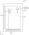
도 1을 참조하면, 표시 장치(1)는 빛을 방출하는 표시영역(DA)과 빛을 방출하지 않는 비표시영역(NDA)을 포함한다. 표시 장치(1)는 표시영역(DA)에 배치된 복수의 화소들에서 방출되는 빛을 이용하여 소정의 이미지를 제공할 수 있다.Referring to FIG. 1 , the
표시 장치(1)는 표시영역(DA)에 의해 적어도 부분적으로 둘러싸인 개구영역(OA)을 포함한다. 이와 관련하여, 도 1은 개구영역(OA)이 표시영역(DA)에 의해 전체적으로 둘러싸인 것을 도시한다. 예컨대, 비표시영역(NDA)은 개구영역(OA)을 둘러싸는 제1비표시영역(NDA1), 및 표시영역(DA)의 외곽을 둘러싸는 제2비표시영역(NDA2)을 포함할 수 있다. 제1비표시영역(NDA1)은 개구영역(OA)을 전체적으로 둘러싸고, 표시영역(DA)은 제1비표시영역(NDA1)을 전체적으로 둘러싸며, 제2비표시영역(NDA2)은 표시영역(DA)을 전체적으로 둘러쌀 수 있다.The
이하에서는, 본 발명의 일 실시예에 따른 표시 장치(1)로서, 유기 발광 표시 장치를 예로 하여 설명하지만, 본 발명의 표시 장치는 이에 제한되지 않는다. 다른 실시예로서, 무기 EL 표시 장치(Inorganic Light Emitting Display), 퀀텀닷 발광 표시 장치 (Quantum dot Light Emitting Display) 등과 같이 다양한 방식의 표시 장치가 사용될 수 있다.Hereinafter, an organic light emitting diode display will be exemplified as the
도 2a 내지 도 2d는 본 발명의 실시예들에 따른 표시 장치를 간략하게 나타낸 단면도로서, 도 1의 II-II'선에 따른 단면에 대응할 수 있다.2A to 2D are cross-sectional views schematically illustrating display devices according to exemplary embodiments, and may correspond to a cross-section taken along line II-II′ of FIG. 1 .
도 2a를 참조하면, 표시 장치(1)는 표시 패널(10), 및 표시 패널(10)의 개구영역(OA)과 대응하는 컴포넌트(20)를 포함할 수 있다. 도시되지는 않았으나, 표시 패널(10) 상에는 터치입력을 감지하는 입력감지부재, 편광자(polarizer)와 지연자(retarder) 또는 컬러필터와 블랙매트릭스를 포함하는 반사 방지부재, 및 투명한 윈도우와 같은 구성요소(들)이 더 배치될 수 있다.Referring to FIG. 2A , the
표시 패널(10)은 기판(100), 기판(100) 상에 배치된 표시요소층(200), 및 표시요소층(200)을 커버하는 봉지부재로서 박막 봉지층(300)을 포함할 수 있다.The
기판(100)은 리지드한(rigid) 기판일 수 있다. 예컨대 기판(100)은 SiO2를 주성분으로 하는 투명한 글래스 기판이거나, 강화 플라스틱과 같은 고분자 수지재를 포함하는 기판일 수 있다. 표시요소층(200)은 표시영역(DA)에 배치된 박막트랜지스터(TFT)를 포함하는 화소회로, 및 화소회로와 전기적으로 연결된 유기발광다이오드(organic light-emitting diode, OLED)와 같은 표시요소를 포함한다. 박막 봉지층(300)은 표시요소층(200)을 커버함으로써, 외부로부터 수분이나 오염물질이 표시요소층(200)으로 침투하는 것을 방지할 수 있다. 박막 봉지층(300)은 적어도 하나의 무기봉지층과 적어도 하나의 유기봉지층을 포함할 수 있다.The
표시 패널(10)은 도 2a에 도시된 바와 같이 개구영역(OA)과 대응하며 표시 패널(10)을 관통하는 개구(10H)를 포함할 수 있다. 기판(100), 표시요소층(200) 및 박막 봉지층(300)은 각각 개구영역(OA)과 대응하는 제1 내지 제3개구(100H, 200H, 300H)들을 포함할 수 있으며, 제1 내지 제3개구(100H, 200H, 300H)들이 표시 패널(10)의 개구(10H)를 형성할 수 있다. 제1개구(100H)는 기판(100)의 상면과 하면을 관통하고, 제2개구(200H)는 표시요소층(200)의 최하층부터 최상층까지를 관통하며, 제3개구(300H)는 박막 봉지층(300)을 관통하도록 형성될 수 있다.As shown in FIG. 2A , the
개구영역(OA)은 컴포넌트(20)가 위치하는 영역으로, 도 2a는 컴포넌트(20)가 기판(100)의 아래에 배치된 것을 도시하고 있으나 본 발명은 이에 한정되지 않는다. 다른 실시예로, 도 2b에 도시된 바와 같이 컴포넌트(20)의 적어도 일부는 개구(10H)를 향하는 표시 패널(10)의 측면과 중첩하도록 표시 패널(10)의 개구(10H) 내에 삽입될 수 있다.The opening area OA is an area in which the
컴포넌트(20)는 전자요소일 수 있다. 예컨대, 컴포넌트(20)는 빛이나 음향을 이용하는 전자요소일 수 있다. 예컨대, 전자요소는 적외선 센서와 같이 빛을 수광하여 이용하는 센서, 빛을 수광하여 이미지를 촬상하는 카메라, 빛이나 음향을 출력하고 감지하여 거리를 측정하거나 지문 등을 인식하는 센서, 빛을 출력하는 소형 램프이거나, 소리를 출력하는 스피커 등을 포함할 수 있다. 빛을 이용하는 전자요소의 경우, 가시광, 적외선광, 자외선광 등과 같이 다양한 파장 대역의 빛을 이용할 수 있다. 일부 실시예에서, 개구영역(OA)은 컴포넌트(20)로부터 외부로 출력되거나 외부로부터 전자요소를 향해 진행하는 빛 또는/및 음향이 투과할 수 있는 투과영역(transmission area)으로 이해될 수 있다.
일 실시예로, 표시 패널(10)이 스마트 워치나 차량용 계기판으로 이용되는 경우, 컴포넌트(20)는 시계 바늘이나 소정의 정보(예, 차량 속도 등)를 지시하는 바늘 등을 포함하는 부재일 수 있다. 컴포넌트(20)는 도 2a 또는 도 2b에 도시된 바와 같이 표시 패널(10)의 개구(10H)와 대응하는 위치에 배치될 수 있는 구성요소로서, 전술한 바와 같이 표시 패널(10)의 기능과 관계된 구성요소(들)를 포함하거나, 표시 패널(10)의 심미감을 증가시키는 액세서리와 같은 구성요소를 포함할 수 있다.In one embodiment, when the
도 2a 및 도 2b에서 기판(100), 표시요소층(200) 및 박막 봉지층(300) 각각이 개구영역(OA)과 대응하는 제1 내지 제3개구(100H, 200H, 300H)들을 구비하는 것과 달리, 기판(100)은 도 2c에 도시된 바와 같이 제1개구(100H)를 포함하지 않을 수 있다.In FIGS. 2A and 2B , each of the
도 2c를 참조하면, 기판(100)이 제1개구(100H)를 포합하지 않지만 표시요소층(200) 및 박막 봉지층(300)은 각각 제2 내지 제3개구(200H, 300H)들을 포함할 수 있다. 일 실시예로, 도 2c에 도시된 표시 패널(10)의 개구영역(OA)에서의 광 투과율은 약 50% 이상, 보다 바람직하게 70% 이상이거나, 75% 이상이거나 80% 이상이거나, 85% 이상이거나 90% 이상일 수 있다.Referring to FIG. 2C , although the
컴포넌트(20)는 개구영역(OA)에 배치되되, 도 2c에 실선으로 도시된 바와 같이 개구(10H)를 향하는 표시 패널(10)의 측면과 비중첩하도록 배치되거나, 도 2c의 점선으로 도시된 바와 같이 표시 패널(10)의 측면과 중첩하도록 적어도 일부가 제2 내지 제3개구(200H, 300H) 내에 삽입될 수 있다.The
도 2d를 참조하면, 기판(100)과 박막 봉지층(300)은 각각 제1개구(100H) 및 제3개구(300H)를 포함하지 않으나, 표시요소층(200)은 제2개구(200H)를 포함할 수 있다. 도 2d에는 컴포넌트(20)가 개구영역(OA)에 배치되되, 개구(10H)를 향하는 표시 패널(10)의 측면과 비중첩하도록 배치된 것을 도시하나, 앞서 도 2c에 점선으로 도시된 위치에 구비될 수 있다.Referring to FIG. 2D , the
도 3은 본 발명의 일 실시예에 따른 표시 패널을 개략적으로 나타낸 평면도이고, 도 4는 표시 패널의 어느 한 화소를 개략적으로 나타낸 등가 회로도이다.3 is a plan view schematically illustrating a display panel according to an exemplary embodiment, and FIG. 4 is an equivalent circuit diagram schematically illustrating one pixel of the display panel.
도 3을 참조하면, 표시 패널(10)은 표시영역(DA)에 배치된 복수의 화소(P)들을 포함한다. 화소(P)들은 각각 유기발광다이오드(OLED)를 포함할 수 있다. 각 화소(P)는 유기발광다이오드를 통해 예컨대, 적색, 녹색, 청색 또는 백색의 빛을 방출할 수 있다.Referring to FIG. 3 , the
도 4를 참조하면, 각 화소(P)는 화소회로(PC), 및 화소회로(PC)에 연결된 유기발광다이오드(OLED)를 포함한다. 화소회로(PC)는 제1박막트랜지스터(T1), 제2박막트랜지스터(T2), 및 스토리지 커패시터(Cst)를 포함할 수 있다.Referring to FIG. 4 , each pixel P includes a pixel circuit PC and an organic light emitting diode OLED connected to the pixel circuit PC. The pixel circuit PC may include a first thin film transistor T1 , a second thin film transistor T2 , and a storage capacitor Cst.
제2박막트랜지스터(T2)는 스위칭 박막트랜지스터로서, 스캔라인(SL) 및 데이터라인(DL)에 연결되며, 스캔라인(SL)으로부터 입력되는 스위칭 전압에 따라 데이터라인(DL)으로부터 입력된 데이터 전압을 제1박막트랜지스터(T1)로 전달한다. 스토리지 커패시터(Cst)는 제2박막트랜지스터(T2)와 구동전압선(PL)에 연결되며, 제2박막트랜지스터(T2)로부터 전달받은 전압과 구동전압선(PL)에 공급되는 제1전원전압(ELVDD)의 차이에 해당하는 전압을 저장한다.The second thin film transistor T2 is a switching thin film transistor, connected to the scan line SL and the data line DL, and a data voltage input from the data line DL according to the switching voltage input from the scan line SL. is transferred to the first thin film transistor T1. The storage capacitor Cst is connected to the second thin film transistor T2 and the driving voltage line PL, and the voltage received from the second thin film transistor T2 and the first power voltage ELVDD supplied to the driving voltage line PL. Store the voltage corresponding to the difference between
제1박막트랜지스터(T1)는 구동 박막트랜지스터로서, 구동전압선(PL)과 스토리지 커패시터(Cst)에 연결되며, 스토리지 커패시터(Cst)에 저장된 전압 값에 대응하여 구동전압선(PL)으로부터 유기발광다이오드(OLED)를 흐르는 구동 전류를 제어할 수 있다. 유기발광다이오드(OLED)는 구동 전류에 의해 소정의 휘도를 갖는 빛을 방출할 수 있다. 유기발광다이오드(OLED)의 대향전극(예, 캐소드)는 제2전원전압(ELVSS)을 공급받을 수 있다.The first thin film transistor T1 is a driving thin film transistor, which is connected to the driving voltage line PL and the storage capacitor Cst, and is output from the driving voltage line PL in response to the voltage value stored in the storage capacitor Cst. The driving current flowing through the OLED) can be controlled. The organic light emitting diode (OLED) may emit light having a predetermined luminance by a driving current. The opposite electrode (eg, a cathode) of the organic light emitting diode OLED may receive the second power supply voltage ELVSS.
도 4는 화소회로(PC)가 2개의 박막트랜지스터와 1개의 스토리지 커패시터를 포함하는 것을 설명하고 있으나, 본 발명은 이에 한정되지 않는다. 박막트랜지스터의 개수 및 스토리지 커패시터의 개수는 화소회로(PC)의 설계에 따라 다양하게 변경될 수 있음은 물론이다.4 illustrates that the pixel circuit PC includes two thin film transistors and one storage capacitor, but the present invention is not limited thereto. Of course, the number of thin film transistors and the number of storage capacitors may be variously changed according to the design of the pixel circuit PC.
다시 도 3을 참조하면, 제1비표시영역(NDA1)은 개구영역(OA)을 둘러쌀 수 있다. 제1비표시영역(NDA1)은 빛을 방출하는 표시요소가 배치되지 않은 영역으로, 제1비표시영역(NDA1)에는 개구영역(OA) 주변에 구비된 화소(P)들에 연결된 배선, 예컨대 신호라인들이 지나가거나 후술할 그루브가 배치될 수 있다. 제2비표시영역(NDA2)에는 각 화소(P)에 스캔신호를 제공하는 스캔 드라이버(1100), 각 화소(P)에 데이터신호를 제공하는 데이터 드라이버(1200), 및 제1 및 제2전원전압을 제공하기 위한 메인 전원배선(미도시) 등이 배치될 수 있다.Referring back to FIG. 3 , the first non-display area NDA1 may surround the opening area OA. The first non-display area NDA1 is an area in which a display element emitting light is not disposed. In the first non-display area NDA1 , a line connected to the pixels P provided around the opening area OA, for example, is Signal lines may pass or a groove to be described later may be disposed. The second non-display area NDA2 includes a
도 3은 표시 패널(10) 중 기판(100)의 모습으로 이해될 수 있다. 예컨대, 기판(100)이 개구영역(OA), 표시영역(DA), 제1 및 제2비표시영역(NDA1, NDA2)를 갖는 것으로 이해될 수 있다.3 may be understood as a view of the
도 5는 본 발명의 일 실시예에 따른 표시 패널의 일부를 나타낸 평면도로서, 제1비표시영역에 위치하는 라인들을 나타낸다.5 is a plan view illustrating a portion of a display panel according to an exemplary embodiment of the present invention, showing lines positioned in a first non-display area.
도 5를 참조하면, 개구영역(OA)을 중심으로 화소(P)들이 표시영역(DA)에 배치되며, 개구영역(OA)과 표시영역(DA) 사이에는 제1비표시영역(NDA1)이 위치할 수 있다.Referring to FIG. 5 , the pixels P are disposed in the display area DA with the opening area OA as the center, and a first non-display area NDA1 is formed between the opening area OA and the display area DA. can be located
화소(P)들은 개구영역(OA)을 중심으로 상호 이격될 수 있다. 화소(P)들은 개구영역(OA)을 중심으로 위와 아래에 이격되거나, 개구영역(OA)을 중심으로 좌우로 이격되어 배치될 수 있다.The pixels P may be spaced apart from each other with respect to the opening area OA. The pixels P may be spaced apart above and below the opening area OA or spaced apart from each other left and right with respect to the opening area OA.
화소(P)들에 신호를 공급하는 신호라인들 중 개구영역(OA)과 인접한 신호라인들은 개구영역(OA)을 우회할 수 있다. 표시영역(DA)을 지나는 데이터라인들 중 일부 데이터라인(DL)들은, 개구영역(OA)을 사이에 두고 위와 아래에 배치된 화소(P)들에 데이터신호를 제공하도록 y방향으로 연장되되, 제1비표시영역(NDA1)에서 개구영역(OA)의 가장자리를 따라 우회할 수 있다. 표시영역(DA)을 지나는 스캔라인들 중 일부 스캔라인(SL)들은, 개구영역(OA)을 사이에 두고 좌우에 배치된 화소(P)들에 스캔신호를 제공하도록 x방향으로 연장되되, 제1비표시영역(NDA1)에서 개구영역(OA)의 가장자리를 따라 우회할 수 있다.Among the signal lines supplying signals to the pixels P, signal lines adjacent to the opening area OA may bypass the opening area OA. Some data lines DL among the data lines passing through the display area DA extend in the y-direction to provide data signals to the pixels P disposed above and below the opening area OA therebetween; The first non-display area NDA1 may be bypassed along the edge of the opening area OA. Some of the scan lines SL passing through the display area DA extend in the x direction to provide a scan signal to the pixels P disposed on the left and right with the opening area OA interposed therebetween. The first non-display area NDA1 may be bypassed along the edge of the opening area OA.
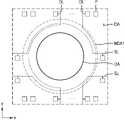
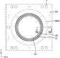
도 6은 본 발명의 일 실시예에 따른 표시 패널의 일부를 나타낸 평면도로서, 제1비표시영역에 위치하는 그루브를 나타낸다.6 is a plan view illustrating a portion of a display panel according to an exemplary embodiment of the present invention, illustrating a groove positioned in a first non-display area.
개구영역(OA)과 표시영역(DA) 사이에는 그루브가 위치한다. 이와 관련하여, 도 6에서는 개구영역(OA)과 표시영역(DA) 사이에 제1 및 제2그루브(G1, G2)가 위치한 것을 도시하지만, 다른 실시예로서, 개구영역(OA)과 표시영역(DA) 사이에는 하나의 그루브만 배치되거나, 3개 이상의 그루브(들)가 위치할 수 있다.A groove is positioned between the opening area OA and the display area DA. In relation to this, although FIG. 6 illustrates that the first and second grooves G1 and G2 are positioned between the opening area OA and the display area DA, as another embodiment, the opening area OA and the display area are shown. Between (DA), only one groove may be disposed, or three or more groove(s) may be located.
제1 및 제2그루브(G1, G2)는 제1비표시영역(NDA1)에서 개구영역(OA)을 전체적으로 둘러싸는 고리형일 수 있다. 도 6에서는 개구영역(OA)이 원형으로 제1 및 제2그루브(G1, G2)가 원형 고리인 것을 도시하고 있으나, 개구영역(OA)은 타원이나 다각형일 수 있으며, 그에 따라 제1 및 제2그루브(G1, G2)도 다양한 형상의 고리 모양을 가질 수 있다. 제1 및 제2그루브(G1, G2) 각각의 직경은 개구영역(OA)의 직경보다는 크게 형성될 수 있으며, 제1 및 제2그루브(G1, G2)는 제1비표시영역(NDA1)에서 소정의 간격 이격되어 배치될 수 있다.The first and second grooves G1 and G2 may have a ring shape that entirely surrounds the opening area OA in the first non-display area NDA1. Although FIG. 6 illustrates that the opening area OA is circular and the first and second grooves G1 and G2 are circular rings, the opening area OA may be an ellipse or a polygon. The two grooves G1 and G2 may also have a ring shape of various shapes. A diameter of each of the first and second grooves G1 and G2 may be greater than a diameter of the opening area OA, and the first and second grooves G1 and G2 are formed in the first non-display area NDA1. They may be disposed to be spaced apart from each other by a predetermined interval.
도 7은 본 발명의 일 실시예에 따른 표시 패널을 나타낸 단면도로서, 도 6의 VII- VII'선에 따른 단면에 해당하고, 도 8은 도 7의 유기발광다이오드를 확대한 단면도이며, 도 9a는 제1그루브를 발췌한 단면도이고, 도 9b는 도 9a의 제1그루브 상의 적층 구조를 나타낸 단면도이다.7 is a cross-sectional view illustrating a display panel according to an embodiment of the present invention, which corresponds to a cross-section taken along line VII-VII' of FIG. 6 , and FIG. 8 is an enlarged cross-sectional view of the organic light emitting diode of FIG. 7 , and FIG. 9A . is a cross-sectional view taken from the first groove, and FIG. 9B is a cross-sectional view illustrating a laminated structure on the first groove of FIG. 9A.
도 7의 표시영역(DA)을 살펴보면, 기판(100)은 전술한 바와 같이 글래스 기판일 수 있다.Referring to the display area DA of FIG. 7 , the
기판(100) 상에는 불순물이 박막트랜지스터의 반도체층으로 침투하는 것을 방지하기 위해 형성된 버퍼층(201)이 배치될 수 있다. 버퍼층(201)은 실리콘 나이트라이드 또는 실리콘옥사이드와 같은 무기 절연물을 포함할 수 있으며, 전술한 무기 절연물을 포함하는 단층 또는 다층일 수 있다.A
버퍼층(201) 상에는 박막트랜지스터(TFT) 및 스토리지 커패시터(Cst) 등을 포함하는 화소회로(PC)가 배치될 수 있다. 박막트랜지스터(TFT)는 반도체층(Act), 게이트전극(GE), 소스전극(SE), 드레인전극(DE)을 포함할 수 있다. 도 7에 도시된 박막트랜지스터(TFT)는 도 4를 참조하여 설명한 구동박막트랜지스터에 대응할 수 있다. 본 실시예에서는 게이트전극(GE)이 게이트절연층(203)을 가운데 두고 반도체층(Act) 상에 배치된 탑 게이트 타입을 도시하였으나, 다른 실시예에 따르면 박막트랜지스터(TFT)는 게이트전극이 게이트절연층의 아래에 배치되고 반도체층이 게이트절연층 위에 배치된 바텀 게이트 타입일 수 있다.A pixel circuit PC including a thin film transistor TFT and a storage capacitor Cst may be disposed on the
반도체층(Act)은 폴리 실리콘을 포함할 수 있다. 또는, 반도체층(Act)은 아모퍼스 실리콘을 포함하거나, 산화물 반도체를 포함하거나, 유기 반도체 등을 포함할 수 있다. 게이트전극(GE)은 저저항 금속 물질을 포함할 수 있다. 게이트전극(GE)은 몰리브덴(Mo), 알루미늄(Al), 구리(Cu), 티타늄(Ti) 등을 포함하는 도전 물질을 포함할 수 있고, 상기의 재료를 포함하는 다층 또는 단층으로 형성될 수 있다.The semiconductor layer Act may include polysilicon. Alternatively, the semiconductor layer Act may include amorphous silicon, an oxide semiconductor, or an organic semiconductor. The gate electrode GE may include a low-resistance metal material. The gate electrode GE may include a conductive material including molybdenum (Mo), aluminum (Al), copper (Cu), titanium (Ti), and the like, and may be formed as a multilayer or single layer including the above material. have.
반도체층(Act)과 게이트전극(GE) 사이의 게이트절연층(203)은 실리콘옥사이드, 실리콘나이트라이드, 실리콘옥시나이트라이드, 알루미늄옥사이드, 티타늄옥사이드, 탄탈륨옥사이드, 하프늄옥사이드 등과 같은 무기 절연물을 포함할 수 있다.The
소스전극(SE) 및 드레인전극(DE)은 전도성이 좋은 재료를 포함할 수 있다. 소스전극(SE) 및 드레인전극(DE)은 몰리브덴(Mo), 알루미늄(Al), 구리(Cu), 티타늄(Ti) 등을 포함하는 도전 물질을 포함할 수 있고, 상기의 재료를 포함하는 다층 또는 단층으로 형성될 수 있다. 일 실시예로, 소스전극(SE) 및 드레인전극(DE)은 Ti/Al/Ti의 다층으로 형성될 수 있다.The source electrode SE and the drain electrode DE may include a material having good conductivity. The source electrode SE and the drain electrode DE may include a conductive material including molybdenum (Mo), aluminum (Al), copper (Cu), titanium (Ti), and the like, and a multilayer including the above material. Alternatively, it may be formed as a single layer. In an embodiment, the source electrode SE and the drain electrode DE may be formed of a multilayer of Ti/Al/Ti.
스토리지 커패시터(Cst)는 제1층간절연층(205)을 사이에 두고 중첩하는 하부 전극(CE1)과 상부 전극(CE2)을 포함한다. 스토리지 커패시터(Cst)는 제2층간절연층(207)으로 커버될 수 있다.The storage capacitor Cst includes a lower electrode CE1 and an upper electrode CE2 that overlap with the first
스토리지 커패시터(Cst)는 박막트랜지스터(TFT)와 중첩될 수 있다. 이와 관련하여, 도 7은 박막트랜지스터(TFT)의 게이트전극(GE)이 스토리지 커패시터(Cst)의 하부 전극(CE1)인 것을 도시하고 있으나, 본 발명은 이에 한정되지 않는다. 다른 실시예로서, 스토리지 커패시터(Cst)는 박막트랜지스터(TFT)와 중첩하지 않을 수 있다.The storage capacitor Cst may overlap the thin film transistor TFT. In this regard, although FIG. 7 illustrates that the gate electrode GE of the thin film transistor TFT is the lower electrode CE1 of the storage capacitor Cst, the present invention is not limited thereto. As another embodiment, the storage capacitor Cst may not overlap the thin film transistor TFT.
제1 및 제2층간절연층(205, 207)은 실리콘옥사이드, 실리콘나이트라이드, 실리콘옥시나이트라이드, 알루미늄옥사이드, 티타늄옥사이드, 탄탈륨옥사이드, 하프늄옥사이드 등과 같은 무기 절연물을 포함할 수 있으며, 단층 또는 다층일 수 있다.The first and second
박막트랜지스터(TFT) 및 스토리지 커패시터(Cst)를 포함하는 화소회로(PC)는 평탄화 절연층(209)으로 커버될 수 있다. 평탄화 절연층(209)은 Polymethylmethacrylate(PMMA)나 Polystylene(PS)과 같은 일반 범용고분자, 페놀계 그룹을 갖는 고분자 유도체, 아크릴계 고분자, 이미드계 고분자, 아릴에테르계 고분자, 아마이드계 고분자, 불소계고분자, p-자일렌계 고분자, 비닐알콜계 고분자 및 이들의 블렌드 등을 포함하는 유기 절연층일 수 있다. 일 실시예로, 평탄화 절연층(209)은 폴리이미드를 포함할 수 있다.The pixel circuit PC including the thin film transistor TFT and the storage capacitor Cst may be covered with a
유기발광다이오드(OLED)는 평탄화 절연층(209) 상에 배치된다. 유기발광다이오드(OLED)의 화소전극(221)은 평탄화 절연층(209) 상에 배치되며 평탄화 절연층(209)의 콘택홀을 통해 화소회로(PC)와 연결될 수 있다.The organic light emitting diode (OLED) is disposed on the
화소전극(221)은 인듐틴옥사이드(ITO; indium tin oxide), 인듐징크옥사이드(IZO; indium zinc oxide), 징크옥사이드(ZnO; zinc oxide), 인듐옥사이드(In2O3: indium oxide), 인듐갈륨옥사이드(IGO; indium gallium oxide) 또는 알루미늄징크옥사이드(AZO; aluminium zinc oxide)와 같은 도전성 산화물을 포함할 수 있다. 다른 실시예로, 화소전극(221)은 은(Ag), 마그네슘(Mg), 알루미늄(Al), 백금(Pt), 팔라듐(Pd), 금(Au), 니켈(Ni), 네오디뮴(Nd), 이리듐(Ir), 크로뮴(Cr) 또는 이들의 화합물을 포함하는 반사막을 포함할 수 있다. 또 다른 실시예로, 화소전극(221)은 전술한 반사막의 위/아래에 ITO, IZO, ZnO 또는 In2O3로 형성된 막을 더 포함할 수 있다.The
화소정의막(211)은 화소전극(221)의 상면을 노출하는 개구를 포함하되, 화소전극(221)의 가장자리를 커버한다. 화소정의막(211)은 유기절연물을 포함할 수 있다. 화소정의막(211)은 전술한 평탄화 절연층(209)에서 설명한 유기 절연물을 포함하거나 또는/및 무기 절연물을 포함할 수 있다. 일 실시예로서 화소정의막(211)은 폴리이미드를 포함할 수 있다.The
중간층(222)은 발광층을 포함한다. 발광층은 소정의 색상의 빛을 방출하는 고분자 또는 저분자 유기물을 포함할 수 있다. 일 실시예로, 중간층(222)은 도 8에 도시된 바와 같이 발광층(222b)의 아래에 배치된 제1기능층(222a) 및/또는 발광층(222b)의 위에 배치된 제2기능층(222c)을 포함할 수 있다.The
제1기능층(222a)은 단층 또는 다층일 수 있다. 예컨대 제1기능층(222a)이 고분자 물질로 형성되는 경우, 제1기능층(222a)은 단층구조인 홀 수송층(HTL: Hole Transport Layer)으로서, 폴리에틸렌 디히드록시티오펜(PEDOT: poly-(3,4)-ethylene-dihydroxy thiophene)이나 폴리아닐린(PANI: polyaniline)으로 형성할 수 있다. 제1기능층(222a)이 저분자 물질로 형성되는 경우, 제1기능층(222a)은 홀 주입층(HIL: Hole Injection Layer)과 홀 수송층(HTL)을 포함할 수 있다.The first
제2기능층(222c)은 반드시 구비되는 것은 아니다. 예컨대, 제1기능층(222a)과 발광층(222b)을 고분자 물질로 형성하는 경우, 유기발광다이오드(OLED)의 특성이 우수해지도록 하기 위해, 제2기능층(222c)을 형성하는 것이 바람직하다. 제2기능층(222c)은 단층 또는 다층일 수 있다. 제2기능층(222c)은 전자 수송층(ETL: Electron Transport Layer) 및/또는 전자 주입층(EIL: Electron Injection Layer)을 포함할 수 있다.The second
중간층(222)을 이루는 복수의 층들 중 일부, 예컨대 기능층(들)은 표시영역(DA)뿐만 아니라 제1비표시영역(NDA1)에도 배치될 수 있으며, 제1비표시영역(NDA1)에서 후술할 제1 및 제2그루브(G1, G2)에 의해 단절된다.Some of the plurality of layers constituting the
대향전극(223)은 중간층(222)을 사이에 두고 화소전극(221)과 마주보도록 배치된다. 대향전극(223)은 일함수가 낮은 도전성 물질로 이루어질 수 있다. 예컨대, 대향전극(223)은 은(Ag), 마그네슘(Mg), 알루미늄(Al), 백금(Pt), 팔라듐(Pd), 금(Au), 니켈(Ni), 네오디뮴(Nd), 이리듐(Ir), 크로뮴(Cr), 리튬(Li), 칼슘(Ca) 또는 이들의 합금 등을 포함하는 (반)투명층을 포함할 수 있다. 또는, 대향전극(223)은 전술한 물질을 포함하는 (반)투명층 상에 ITO, IZO, ZnO 또는 In2O3과 같은 층을 더 포함할 수 있다.The
유기발광다이오드(OLED)는 박막 봉지층(300)으로 커버된다. 박막 봉지층(300)은 적어도 하나의 유기봉지층 및 적어도 하나의 무기봉지층을 포함할 수 있다. 도 7에는 박막 봉지층(300)이 제1 및 제2무기봉지층(310, 330) 및 이들 사이에 개재된 유기봉지층(320)을 포함하는 것을 도시하고 있으나, 다른 실시예에서 적층 순서와 개수는 변경될 수 있다.The organic light emitting diode (OLED) is covered with a thin
제1 및 제2무기봉지층(310, 330)은 알루미늄옥사이드, 티타늄옥사이드, 탄탈륨옥사이드, 하프늄옥사이드, 아연옥사이드, 실리콘옥사이드, 실리콘나이트라이드, 실리콘옥시나이트라이드 하나 이상의 무기 절연물을 포함할 수 있으며, 화학기상증착법(CVD) 등에 의해 형성될 수 있다. 유기봉지층(320)은 폴리머(polymer)계열의 소재를 포함할 수 있다. 폴리머 계열의 소재로는 아크릴계 수지, 에폭시계 수지, 폴리이미드 및 폴리에틸렌 등을 포함할 수 있다.The first and second inorganic encapsulation layers 310 and 330 may include one or more inorganic insulating materials such as aluminum oxide, titanium oxide, tantalum oxide, hafnium oxide, zinc oxide, silicon oxide, silicon nitride, silicon oxynitride, It may be formed by chemical vapor deposition (CVD) or the like. The
도 7의 제1비표시영역(NDA1)을 참조하면, 제1비표시영역(NDA1)은 개구영역(OA)에서 상대적으로 먼 제1서브-비표시영역(SNDA1) 및 개구영역(OA)에 상대적으로 가까운 제2서브-비표시영역(SNDA2)을 포함할 수 있다.Referring to the first non-display area NDA1 of FIG. 7 , the first non-display area NDA1 is located in the first sub-non-display area SNDA1 and the opening area OA relatively far from the opening area OA. A relatively close second sub-non-display area SNDA2 may be included.
제1서브-비표시영역(SNDA1)은 배선, 예컨대 도 5를 참조하여 설명한 신호라인들이 지나는 영역일 수 있다. 이와 관련하여, 도 7에서는 제1서브-비표시영역(SNDA1)에 위치하는 데이터라인(DL)들을 도시하고 있으며, 이들은 도 5를 참조하여 설명한 개구영역(OA)을 우회하는 데이터라인들에 해당한다. 데이터라인(DL)들은 절연층(예컨대, 제2층간절연층)을 사이에 두고 교번적으로 배치될 수 있으며, 이 경우 이웃한 데이터라인(DL)들 사이의 거리(피치)를 줄일 수 있고 제1비표시영역(NDA1)의 폭을 줄일 수 있다. 다른 실시예로, 데이터라인(DL)들은 모두 동일한 층 상, 예컨대 제2층간절연층(207) 상에 배치될 수도 있다.The first sub-non-display area SNDA1 may be an area through which wirings, for example, the signal lines described with reference to FIG. 5 pass. In this regard, FIG. 7 illustrates data lines DL positioned in the first sub-non-display area SNDA1, which correspond to data lines bypassing the open area OA described with reference to FIG. 5 . do. The data lines DL may be alternately disposed with an insulating layer (eg, a second interlayer insulating layer) interposed therebetween. In this case, the distance (pitch) between neighboring data lines DL may be reduced and the 1 The width of the non-display area NDA1 may be reduced. In another embodiment, all of the data lines DL may be disposed on the same layer, for example, on the second
도 7에는 제1서브-비표시영역(SNDA1)에 데이터라인(DL)들을 도시하고 있으나, 앞서 도 5를 참조하여 설명한 개구영역(OA)을 우회하는 스캔라인들도 제1서브-비표시영역(SNDA1)에 위치할 수 있음은 물론이다.Although the data lines DL are shown in the first sub-non-display area SNDA1 in FIG. 7 , the scan lines bypassing the opening area OA described with reference to FIG. 5 are also in the first sub-non-display area. Of course, it may be located in (SNDA1).
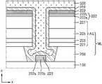
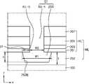
제2서브-비표시영역(SNDA2)은 제1 및 제2그루브(G1, G2)가 위치하는 영역일 수 있다. 제1 및 제2그루브(G1, G2)는 기판(100) 상에 배치된 다층 막(ML)에 형성된다. 다층 막(ML)은 하부 절연층(250) 및 하부 절연층(250) 위에 배치된 적어도 하나의 절연층(AIL)을 포함한다. 하부 절연층(250)은 기판(100)과 화소회로(PC) 사이, 예컨대 기판(100)과 박막트랜지스터(TFT) 사이에 개재될 수 있다. 이와 관련하여, 도 7에는 기판(100)의 바로 위에 하부 절연층(250)이 배치된 것을 도시한다. 적어도 하나의 절연층(AIL)은 무기 절연층을 포함할 수 있는데, 도 7에는 적어도 하나의 절연층(AIL)이 버퍼층(201), 게이트절연층(203), 제1층간절연층(205) 및 제2층간절연층(207)을 포함하는 것을 도시한다. 적어도 하나의 절연층(AIL)은 버퍼층(201), 게이트절연층(203), 제1층간절연층(205) 또는 제2층간절연층(207) 중에서 선택된 하나 이상의 절연층(들)을 나타낼 수 있다.The second sub-non-display area SNDA2 may be an area in which the first and second grooves G1 and G2 are located. The first and second grooves G1 and G2 are formed in the multilayer film ML disposed on the
제1 및 제2그루브(G1, G2)는 다층 막(ML)의 두께 방향을 따라 소정의 깊이를 갖도록 형성되되, 각각의 제1 및 제2그루브(G1, G2)는 깊이 방향을 따라 하부 절연층(250)을 지나는 부분의 폭이 적어도 하나의 절연층(AIL)을 지나는 부분의 폭 보다 큰 언더컷 구조를 가질 수 있다. 적어도 하나의 절연층(AIL)은 무기절연층이고, 하부 절연층(250)은 유기절연층인 것과 같이 적어도 하나의 절연층(AIL)과 하부 절연층(250)은 서로 다른 물질을 포함할 수 있다. 하부 절연층(250)은 예를 들어 폴리이미드를 포함할 수 있다.The first and second grooves G1 and G2 are formed to have a predetermined depth along the thickness direction of the multilayer film ML, and each of the first and second grooves G1 and G2 has a lower insulation along the depth direction. The undercut structure may have an undercut structure in which a width of a portion passing through the
도 9a를 참조하면, 깊이 방향을 따라 제1그루브(G1) 중 하부 절연층(250)을 지나는 부분의 제1폭(W1)은 제1그루브(G1) 중 적어도 하나의 절연층(AIL)을 지나는 부분의 제2폭(W2) 보다 크다. 적어도 하나의 절연층(AIL)의 측면은 제1그루브(G1)의 중심을 향해 하부 절연층(250)의 측면(250IE)보다 더 돌출될 수 있으며, 적어도 하나의 절연층(AIL)의 돌출된 부분은 팁(또는 처마)을 형성할 수 있다. 이와 관련하여, 도 9a에는 한쌍의 팁(또는 처마)를 도시하고 있다. 팁은 약 0.9㎛ 내지 1.2㎛ 정도 x방향을 따라 하부 절연층(250)의 측면(250IE)보다 더 돌출될 수 있다.Referring to FIG. 9A , a first width W1 of a portion of the first groove G1 passing through the lower insulating
제1그루브(G1)는 적어도 어느 하나의 절연층(AIL) 및 하부 절연층(250)을 식각하여 형성할 수 있다. 적어도 하나의 절연층(AIL)의 일부를 제거하는 식각 공정에서 사용하는 에천트 또는 식각 가스는 하부 절연층(250)의 일부를 제거하는 식각 공정에서 사용하는 에천트 또는 식각 가스와 서로 다른 물질을 포함할 수 있다.The first groove G1 may be formed by etching at least one of the insulating layer AIL and the lower insulating
식각 공정을 통해 하부 절연층(250)에는 제1홀(250H)이 형성되고, 적어도 하나의 절연층(AIL)에는 제2홀(AIL-H)이 형성되며, 제1홀(250H)과 제2홀(AIL-H)은 서로 연결되어 제1그루브(G1)를 이룰 수 있다. 제1홀(250H)의 제1폭(W1)은 제2홀(AIL-H)의 제2폭(W2) 보다 크게 형성되며, 제1그루브(G1)는 하부의 폭이 상부의 폭 보다 큰 언더컷 구조를 가질 수 있다. 이와 관련하여 도 9a에는 제2홀(AIL-H)을 정의하는 적어도 하나의 절연층(AIL)의 측면(AIL-IE)이 제1홀(250H)을 정의하는 하부 절연층(250)의 측면(250IE) 보다 제1그루브(G1)의 중심을 향해 측방향(lateral direction, x방향)을 따라 제1거리(d1)만큼 더 돌출된 것을 나타낸다.Through the etching process, a
제1거리(d1)는 하부 절연층(250)의 두께(t)보다 작거나, 하부 절연층(250)의 두께(t)와 같거나, 하부 절연층(250)의 두께(t)보다 클 수 있다. 제1거리(d1)는 제1무기봉지층(310)의 두께 보다 크게 형성되거나, 제1 및 제2무기봉지층(310, 330)의 두께들의 합 보다 크게 형성될 수 있다. 일 실시예로, 제1거리(d1)는 약 1μm이거나 그 보다 크게 형성될 수 있다. 즉, 팁은 하부 절연층(250)의 측면(250IE)보다 제1거리(d1)만큼 더 돌출될 수 있다.The first distance d1 is less than the thickness t of the lower insulating
도 9a에 도시된 바와 같이 다층 막(ML)에 제1그루브(G)가 형성된 이후에, 중간층(222) 및 대향전극(223)이 열 증착법 등에 의해 형성될 수 있다. 중간층(222)을 이루는 복수의 층들 중 일부, 예컨대 제1 또는/및 제2기능층(222a, 222c)과 대향전극(223)은 기판(100) 상에 증착될 수 있는데, 이 때 제1비표시영역(NDA1)에 위치하는 제1 및 제2그루브(G1, G2)에 의해 단절될 수 있다. 이와 관련하여, 도 9b는 중간층(222)의 제1 또는/및 제2기능층(222a, 222c)과 대향전극(223)이 제1그루브(G1)에 의해 단절된 것을 도시한다.As shown in FIG. 9A , after the first groove G is formed in the multilayer film ML, the
도 9a 및 도 9b에서는 제1그루브(G1)를 중심으로 설명하였으나, 제2그루브(G2)도 제1그루브(G1)와 동일한 구조를 가지며, 제2그루브(G2)를 중심으로 제1 또는/및 제2기능층(222a, 222c)과 대향전극(223)이 단절됨은 앞서 설명한 바와 같다.9A and 9B, the first groove G1 has been mainly described, but the second groove G2 also has the same structure as the first groove G1, and the first groove G2 is the center of the first groove G2. and the second
다시 도 7를 참조하면, 박막 봉지층(300)은 제1비표시영역(NDA1)도 커버한다. 화학기상증착법(CVD) 등으로 형성되는 제1무기봉지층(310)은 중간층(222) 및 대향전극(223)과 달리 스텝 커버리지가 상대적으로 우수하므로, 제1 및 제2그루브(G1, G2)의 내부 표면(inner surface)을 전체적으로 커버할 수 있다. 도 9b에 도시된 바와 같이, 제1무기봉지층(310)은 제1그루브(G1)를 형성하는 하부 절연층(250)의 측면(250IE)과 바닥면, 그리고 적어도 하나의 절연층(AIL)의 측면(AIL-IE)과 바닥면을 커버할 수 있다. 여기서, 하부 절연층(250)의 바닥면은 기판(100)의 상면에 대응할 수 있고, 적어도 하나의 절연층(AIL)의 바닥면은 버퍼층(201)의 하부면에 대응할 수 있다.Referring back to FIG. 7 , the thin
제1무기봉지층(310)은 제1 및 제2그루브(G1, G2) 내에 위치하는 단절된 제1 및 제2기능층(222a, 222c)과 대향전극(233)을 커버하며, 제1그루브(G1)를 통해 노출된 기판(100)의 상면과 직접 접촉할 수 있다. 제1무기봉지층(310)의 두께, 예컨대 기판(100)에 수직한 방향(z방향)으로의 두께는 하부 절연층(250)의 두께(t) 보다 작은 두께를 가질 수 있다. 제1그루브(G1) 중 일부는 제1무기봉지층(310) 상의 유기봉지층(320)으로 채워질 수 있다. The first
유기봉지층(320)은 표시영역(DA)뿐만 아니라 제1비표시영역(NDA1)의 일부를 커버할 수 있다. 예컨대, 유기봉지층(320)의 단부(320E)는 제1그루브(G1)와 제2그루브(G2) 사이에 위치할 수 있다. 유기봉지층(320)은 기판(100) 상에 모노머 등을 도포한 후 이를 경화시켜 형성될 수 있는데, 유기봉지층(320)이 개구(10H)에 노출되는 경우, 유기봉지층(320)을 통해 투습이 진행될 수 있다. 이를 방지하기 위하여, 유기봉지층(320) 중 일부, 예컨대 개구영역(OA)과 제1그루브(G1) 사이의 영역(HA)에 해당하는 부분을 에슁 등으로 제거할 수 있다. 따라서 기판(100)의 상면에 수직한 방향에서 보았을 때, 유기봉지층(320)이 구비되지 않는 전술한 영역(HA)이 개구영역(OA)을 둘러싸는 고리 형일 수 있으며, 유기봉지층(320)의 단부(320E)는 제1그루브(G1)와 제2그루브(G2) 사이에 배치될 수 있다.The
유기봉지층(320)의 단부(320E)가 제1 및 제2무기봉지층(310, 330)의 단부 보다 표시영역(DA) 측에 인접하게 배치되면서, 전술한 영역(HA)에서 제1 및 제2무기봉지층(310, 330)은 직접 접촉할 수 있다. 제1 및 제2무기봉지층(310, 330)은 제2그루브(G2) 내에서, 그리고 표시 패널(10)의 개구(10H) 주변에서 서로 접촉할 수 있다.The
개구(10H)를 향하는 기판(100)의 단부(100E)는 표시 패널(10)의 개구(10H)를 향하는 하부 절연층(250)의 단부(250E) 보다 개구(10H)를 향해 더 도출될 수 있다. 도 7에는 단면이 도시되어 있으나, 도 6과 도 7을 함께 고려하여 보건대 기판(100)의 상면에 수직한 방향에서 보았을 때, 기판(100)이 개구영역(OA)에 대응하는 제1개구(100H)를 구비하는 것과 마찬가지로 하부 절연층(250)은 개구영역(OA)에 대응하는 개구(250H)를 포함할 수 있으며, 하부 절연층(250)의 개구(250H)는 기판(100)의 제1개구(100H) 보다 큰 직경을 갖는 것으로 이해할 수 있다.The
기판(100)의 제1개구(100H)는 레이저 커팅 공정 또는 드릴링 공정 등을 통해 형성될 수 있다. 레이저 커팅 또는 드릴링 공정 중 무기절연층인 적어도 하나의 절연층(AIL)에 충격이 가해지는 경우 크랙이 발생할 수 있으며, 크랙을 통해 외부 수분과 같은 이물질이 침투하는 문제가 있을 수 있다. 그러나, 제1 및 제2그루브(G1, G2)를 형성하는 식각 공정에서 개구영역(OA)과 대응하는 다층 막(ML)의 부분을 제거하고, 이 후에 전술한 레이저 커팅이나 드릴링 공정을 수행하는 경우 무기절연층에 크랙이 형성되는 것을 방지할 수 있다. 제2거리(d2)는 레이저 커팅이나 드릴링 공정시 무기절연층에 크랙이 야기되지 않도록 고려된 마진으로 이해될 수 있다. 기판(100)의 단부(100E)와 하부 절연층(250)의 단부(250E) 사이의 제2거리(d2)는 약 0.1μm 이상일 수 있다.The
도 10a는 본 발명의 다른 실시예에 따른 표시 패널의 제1그루브를 나타낸 단면도이고, 도 10b는 도 10a의 제1그루브 상의 적층 구조를 나타낸 단면도이다. 앞서 도 9a 및 도 9b를 참조하여 설명한 제1그루브를 참조하면, 적어도 하나의 절연층(AIL)의 측면(AIL-IE)이 비교적 편평한 면을 갖는다. 반면, 도 10a 및 도 10b을 참조하면, 적어도 하나의 절연층(AIL)에 국소적으로 언더컷 구조가 형성되면서 적어도 하나의 절연층(AIL)의 측면이 요철을 갖는 것을 도시하고 있다.10A is a cross-sectional view illustrating a first groove of a display panel according to another exemplary embodiment of the present invention, and FIG. 10B is a cross-sectional view illustrating a stacked structure on the first groove of FIG. 10A. Referring to the first groove described above with reference to FIGS. 9A and 9B , the side surface AIL-IE of the at least one insulating layer AIL has a relatively flat surface. On the other hand, referring to FIGS. 10A and 10B , a side surface of the at least one insulating layer AIL has irregularities while the undercut structure is locally formed on the at least one insulating layer AIL.
적어도 하나의 절연층(AIL)은 무기절연층, 예컨대 실리콘을 포함하는 복수의 무기절연층으로 형성될 수 있다. 식각 공정에서 버퍼층(201), 게이트절연층(203), 제1층간절연층(205) 및 제2층간절연층(207)이 식각되는 양은 식각 공정에서의 조건(시간, 에천트나 식각 가스의 조성 등)이나 버퍼층(201), 게이트절연층(203), 제1층간절연층(205) 및 제2층간절연층(207)에 포함된 물질 등에 따라 서로 다를 수 있다. 예컨대, 버퍼층(201)과 제1층간절연층(205)이 실리콘옥사이드를 포함하고, 게이트절연층(203)과 제2층간절연층(207)이 실리콘나이트라이드를 포함하는 경우, 동일한 식각 가스를 사용하더라도 식각되는 조건(시간 등)에 따라 도 10a에 도시된 바와 같이 식각되는 양이 다를 수 있다. 버퍼층(201)의 측면(201IE)과 버퍼층(201)의 측면(201IE) 및 제1층간절연층(205)의 측면(205IE)은 이웃한 게이트절연층(203)의 측면(203IE) 및 제2층간절연층(207)의 측면(207IE) 보다 제1그루브(G1)의 중심을 향해 더 도출될 수 있다. 따라서, 적어도 하나의 절연층(AIL)에는 복수의 언더컷 구조가 형성되며, 적어도 하나의 절연층(AIL)의 측면은 요철면을 갖는다. 전술한 요철면은 단순히 오목하고 볼록한 면이 아니라, 적어도 하나의 절연층(AIL)에 구비된 복수의 무기절연층들이 서로 다른 물질을 가지면서 야기된 것으로서, 무기절연층들의 두께 방향으로 물질의 변화에 따른 요철면으로 이해할 수 있다.At least one insulating layer AIL may be formed of an inorganic insulating layer, for example, a plurality of inorganic insulating layers including silicon. The amount of the
도 10a에 도시된 제1그루브(G1)가 형성된 이후에, 중간층(222), 예컨대 제1 및 제2기능층(222a, 222c)과 대향전극(223)이 증착되면서 제1그루브(G1)에 의해 단절되는 것은 앞서 도 9b를 참조하여 설명한 바와 같다. 마찬가지로, 순차적으로 제1무기봉지층(310), 유기봉지층(320) 등이 적층되는 등의 구조도 앞서 설명한 바와 같다.After the first groove G1 shown in FIG. 10A is formed, the
도 11은 본 발명의 다른 실시예에 따른 표시 패널의 단면도로서, 도 6의 VII- VII'선에 따른 단면에 해당하며, 도 12a는 도 11의 제1그루브를 나타낸 단면이고, 도 12b는 제1그루브 상의 적층 구조를 나타낸다. 도 11 내지 도 12b에 도시된 표시 패널은 앞서 도 7 내지 도 9b를 참조하여 설명한 내용과 실질적으로 동일하므로, 이하에서는 차이점을 중심으로 설명한다.11 is a cross-sectional view of a display panel according to another exemplary embodiment of the present invention, which corresponds to a cross-section taken along line VII-VII' of FIG. 6 , FIG. 12A is a cross-sectional view illustrating the first groove of FIG. 11 , and FIG. 12B is a second view The laminated structure on one groove is shown. Since the display panel shown in FIGS. 11 to 12B is substantially the same as that described with reference to FIGS. 7 to 9B , the following description will focus on differences.
도 11을 참조하면, 제1 및 제2그루브(G1, G2)는 다층 막(ML)에 형성되되, 제1 및 제2그루브(G1, G2)의 바닥면은 기판(100)의 상면과 다른 가상의 면 상에 있을 수 있다. 예컨대, 앞서 도 7 및 도 9a를 참조하여 설명한 제1 및 제2그루브(G1, G2)의 바닥면은 기판(100)의 상면과 동일한 가상의 면 상에 배치된 데 반해, 도 11 및 도 12a에 도시된 제1 및 제2그루브(G1, G2)의 바닥면은 기판(100)의 상면 위이면서 하부 절연층(250)의 상면의 아래에 있는 가상의 면 상에 있을 수 있다.Referring to FIG. 11 , the first and second grooves G1 and G2 are formed in the multilayer film ML, and the bottom surfaces of the first and second grooves G1 and G2 are different from the top surface of the
도 12a를 참조하면, 제1그루브(G1)는 다층 막(ML)을 식각하여 형성할 수 있다. 적어도 하나의 절연층(AIL)의 일부를 식각하여 적어도 하나의 절연층(AIL)을 관통하는 제2홀(AIL-h)을 형성하고, 하부 절연층(250)의 일부를 식각하여 하부 절연층(250)을 관통하지 않는 제1리세스(250r)를 형성할 수 있으며, 제1리세스(250r) 및 제2홀(AIL-h)이 제1그루브(G1)를 이룰 수 있다.Referring to FIG. 12A , the first groove G1 may be formed by etching the multilayer film ML. A portion of the at least one insulating layer AIL is etched to form a second hole AIL-h passing through the at least one insulating layer AIL, and a portion of the lower insulating
제1리세스(250r)의 깊이(h)는 하부 절연층(250)의 두께(t)보다 작은 값을 가질 수 있다. 제1리세스(250r)의 깊이(h)는 하부 절연층(250)의 두께(t)의 50% 이상이거나, 60% 이상이거나, 70% 이상이거나, 80%이상이거나, 90%이상이거나, 95%이상이거나, 97%이상일 수 있다. 제1리세스(250r)와 제2홀(AIL-h)은 연결되어 제1그루브(G1)를 이룰 수 있으며, 제1그루브(G1)의 바닥면은 기판(100)의 상면과 하부 절연층(250)의 상면 사이에 위치하는 가상의 면 상에 놓일 수 있다. The depth h of the
하부 절연층(250)이 유기절연층이므로, 제1그루브(G1) 아래에 하부 절연층(250)이 잔존하는 경우, 잔존하는 하부 절연층(250)을 통해 외부의 수분이 유입되고 수분이 무기절연층의 크랙을 통해 유기발광소자(OLED, 도 11)로 유입될 가능성이 미약하게나마 존재할 수 있다. 그러나, 본 발명의 실시예에서와 같이 기판(100)이 리지드한 기판인 경우, 기판(100) 상에 적층된 무기절연층에 크랙이 발생될 가능성이 현저하게 낮거나 없으므로 전술한 문제를 최소화할 수 있다.Since the lower insulating
도 12a에 도시된 바와 같은 제1그루브(G1) 상에 중간층(222), 예컨대 제1 또는/및 제2기능층(222a, 222c) 및 대향전극(223)이 형성되는 경우, 제1 또는/및 제2기능층(222a, 222c) 및 대향전극(223)은 도 12b에 도시된 바와 같이 제1그루브(G1)에서 단절된다.When the
도 11 내지 도 12c를 참조하여 설명한 하부 절연층(250)에 제1홀이 아닌 제1리세스(250r)가 형성된 구조는, 앞서 도 10a 및 도 10b를 참조하여 설명한 제1그루브의 구조 및 이로부터 파생되는 구조에도 동일하게 적용될 수 있다.The structure in which the
도 13은 본 발명의 다른 실시예에 따른 표시 패널을 나타낸 단면도이다.13 is a cross-sectional view illustrating a display panel according to another exemplary embodiment.
도 13의 표시 패널은 앞서 도 7을 참조하여 설명한 표시 패널과 실질적으로 동일한 구조를 포함하되, 제1그루브(G1)와 제2그루브(G2) 사이에 격벽(400)를 더 포함하는 것을 도시한다.The display panel of FIG. 13 has substantially the same structure as the display panel described with reference to FIG. 7 , but further includes a
격벽(400)는 유기절연물을 포함할 수 있으며, 기판(100)의 상면에 수직한 방향에서 보았을 때 개구영역(OA), 예컨대 개구(10H)를 둘러싸는 고리 형상일 수 있다. 격벽(400)는 평탄화 절연층(209)과 동일한 물질을 포함하는 제1서브-격벽층(410) 및 화소정의막(211)과 동일한 물질을 포함하는 제2서브-격벽층(420)을 포함할 수 있다. 격벽(400)는 유기봉지층(320)을 형성하는 공정에서 모노머의 흐름을 제어할 수 있다.The
도 13에 도시된 격벽(400)는 도 10a 및 도 10b를 참조하여 설명한 제1 및 제2그루브를 갖는 표시 패널이나, 도 11 내지 도 12b를 참조하여 설명한 제1 및 제2그루브를 갖는 표시 패널이나, 이들로부터 파생되는 다양한 표시 패널 등에도 구비될 수 있음은 물론이다.The
도 14는 본 발명의 다른 실시예에 따른 표시 패널을 나타낸 단면도로서, 도 6의 VII- VII '선에 따른 단면이고, 도 15a는 본 발명의 다른 실시예에 따른 표시 패널의 제1그루브를 나타낸 단면도이고, 도 15b는 도 15a의 제1그루브 상의 적층 구조를 나타낸 단면도이다. 도 14의 표시 패널은 하부 절연층(250') 및 하부 절연층(250')을 중심으로 한 제1 및 제2그루브의 구조를 제외한 나머지 구성요소는 앞서 도 7 등을 참조하여 설명한 표시 패널과 실질적으로 동일하므로 이하에서는 차이를 중심으로 설명한다.14 is a cross-sectional view of a display panel according to another embodiment of the present invention, taken along line VII-VII' of FIG. 6, and FIG. 15A is a first groove of the display panel according to another embodiment of the present invention. 15B is a cross-sectional view illustrating a laminated structure on the first groove of FIG. 15A. In the display panel of FIG. 14 , except for the structure of the first and second grooves centered on the lower insulating
도 14의 표시 패널에서 하부 절연층(250')은 무기절연층을 포함할 수 있다. 하부 절연층(250')은 적어도 하나의 절연층(AIL)과 다른 무기절연층을 포함할 수 있다. 예컨대, 하부 절연층(250')은 실리콘나이트라이드나 실리콘옥시카바이드(SiOC)와 같은 물질을 포함할 수 있다.In the display panel of FIG. 14 , the lower insulating
제1 및 제2그루브(G1, G2)는 적어도 하나의 절연층(AIL) 및 하부 절연층(250')을 식각하여 형성할 수 있다. 적어도 하나의 절연층(AIL)의 식각 공정과 하부 절연층(250')의 식각 공정은 동일한 에천트 또는 식각 가스를 사용하거나 서로 다른 에천트 또는 식각 가스를 사용할 수 있다.The first and second grooves G1 and G2 may be formed by etching at least one insulating layer AIL and the lower insulating
일 실시예로, 하부 절연층(250')이 실리콘나이트라이드나 실리콘옥시카바이드를 포함하고, 버퍼층(201)과 게이트절연층(203) 및 하부 제2층간절연층(207a)이 실리콘옥사이드를 포함하며, 제1층간절연층(205)과 상부 제2층간절연층(207b)이 실리콘나이트라이드를 포함하는 경우, 도 15a에 도시된 바와 같이 식각되는 양이 서로 다를 수 있다.In an embodiment, the lower insulating
하부 절연층(250') 바로 위의 버퍼층(201)과 게이트절연층(203)의 측면(201IE, 203IE)들은 하부 절연층(250')의 측면(250'IE) 보다 제1그루브(G1)의 중심을 향해 더 돌출되어 언더컷 구조를 형성할 수 있다. 하부 제2층간절연층(207a)의 측면(207aIE)은 제1층간절연층(205)의 측면(205IE) 보다 제1그루브(G1)의 중심을 향해 더 돌출되어 언더컷 구조를 가질 수 있다.The side surfaces 201IE and 203IE of the
도 15a에서는 제2층간절연층(207)이 서로 다른 물질을 갖는 다층으로서, 하부 및 상부 제2층간절연층(207a, 207b)의 측면(207aIE, 207bIE)들이 단차를 형성하는 것을 도시하고 있으나, 본 발명은 이에 한정되지 않는다. 다른 실시예로서, 버퍼층(201), 게이트절연층(203), 및 제1층간절연층(205)도 서로 다른 물질을 갖는 다층 구조를 가질 수 있으며, 이 경우 적어도 하나의 절연층(AIL)은 국소적으로 다양한 형상의 언더컷 구조를 가질 수 있다.15A shows that the second
무기절연층인 하부 절연층(250')의 측면(250'IE)은 앞서 도 9a를 참조하여 설명한 유기절연층인 하부 절연층(250)의 측면(250IE) 보다 경사각(β, β>α)이 클 수 있다. 예컨대, 하부 절연층(250')의 측면(250'IE)의 경사각(β)은 80°이상이거나, 85°이상일 수 있다.The side surface 250'IE of the lower insulating layer 250', which is an inorganic insulating layer, has an inclination angle (β, β>α) than the side surface 250IE of the lower insulating
도 15a의 제1그루브(G1)가 형성된 이후, 중간층(222), 예컨대 제1 또는/및 제2기능층(222a, 222c)과 대향전극(223)이 증착되면서 제1그루브(G1)에 의해 단절될 수 있다. 이 후, 순차적으로 제1무기봉지층(310), 유기봉지층(320) 등이 적층되는 구조등은 앞서 도 7 및 도 9b 등을 참조하여 설명한 바와 같다.After the first groove G1 of FIG. 15A is formed, the
도 16은 본 발명의 다른 실시예에 따른 표시 패널을 나타낸 단면도로서, 도 6의 VII- VII '선에 따른 단면이다. 도 16의 표시 패널은 도 14에 도시된 표시 패널과 실질적으로 동일하므로, 이하에서는 차이점을 중심으로 설명한다.16 is a cross-sectional view illustrating a display panel according to another exemplary embodiment of the present invention, and is a cross-sectional view taken along line VII-VII' of FIG. 6 . Since the display panel of FIG. 16 is substantially the same as the display panel of FIG. 14 , differences will be mainly described below.
도 16을 참조하면, 제1 및 제2그루브(G1, G2)는 다층 막(ML)에 형성되되, 제1 및 제2그루브(G1, G2)의 바닥면은 기판(100)의 상면과 다른 가상의 면 상에 있을 수 있다. 앞서 도 14 를 참조하여 설명한 제1 및 제2그루브(G1, G2)의 바닥면은 기판(100)의 상면과 동일한 가상의 면 상에 배치된 데 반해, 도 16에 도시된 제1 및 제2그루브(G1, G2)의 바닥면은 기판(100)의 상면 위이면서 하부 절연층(250')의 상면의 아래에 있는 가상의 면 상에 있을 수 있다.Referring to FIG. 16 , the first and second grooves G1 and G2 are formed in the multilayer film ML, and the bottom surfaces of the first and second grooves G1 and G2 are different from the top surface of the
제1 및 제2그루브(G1, G2) 중 하부 절연층(250')을 지나는 부분은, 하부 절연층(250')의 일부가 식각되면서 형성된 것으로, 하부 절연층(250')에는 앞서 도 12a를 참조하여 설명한 바와 같이 리세스가 형성될 수 있다. 리세스의 깊이(h)는 하부 절연층(250')의 두께(t) 보다 작은 값을 가질 수 있다. 예컨대, 하부 절연층(250')의 리세스의 깊이(h)는 하부 절연층(250')의 두께(t)의 50% 이상이거나, 60% 이상이거나, 70% 이상이거나, 80%이상이거나, 90%이상이거나, 95%이상이거나, 97%이상일 수 있다.A portion of the first and second grooves G1 and G2 passing through the lower insulating
도 17은 본 발명의 다른 실시예에 따른 표시 패널을 개략적으로 나타낸 단면도이다. 도 17의 표시 패널은 도 14에 도시된 표시 패널과 실질적으로 동일하므로, 이하에서는 차이점을 중심으로 설명한다.17 is a cross-sectional view schematically illustrating a display panel according to another exemplary embodiment. Since the display panel of FIG. 17 is substantially the same as the display panel of FIG. 14 , differences will be mainly described below.
도 17을 참조하면, 제1그루브(G1)와 제2그루브(G2) 사이에 격벽(400)가 배치될 수 있다. 격벽(400)는 제1 및 제2서브-격벽층(410, 420)을 포함하며, 그 물질은 도 13을 참조하여 설명한 바와 같다. 격벽(400)는 유기봉지층(320)의 형성시 모노머의 흐름을 제어할 수 있으므로, 모노머가 경화되면서 형성된 유기봉지층(320)의 단부는 격벽(400)의 일 측면과 인접하게 배치될 수 있다. 유기봉지층(320)의 단부는 격벽(400)를 넘어서 개구(10H)를 향해 연장되지 않는다. 도 17에 도시된 격벽(400)는 도 16을 참조하여 설명한 표시 패널에도 구비될 수 있음은 물론이다.Referring to FIG. 17 , a
도 18은 본 발명의 다른 실시예에 따른 표시 패널을 나타낸 평면도이고, 도 19는 도 18의 개구영역 주변을 나타낸 평면도이다. 도 18의 표시 패널(10') 중 도 3 내지 도 6을 참조하여 설명한 표시 패널(10)과 동일한 구성 및 구조에 대해서는 앞서 설명한 내용으로 갈음하고, 이하에서는 차이점을 중심으로 설명한다.18 is a plan view illustrating a display panel according to another exemplary embodiment, and FIG. 19 is a plan view illustrating the periphery of the opening area of FIG. 18 . The same configuration and structure as those of the
도 18 및 도 19를 참조하면, 개구영역(OA)은 표시영역(DA)에 의해 부분적으로 둘러싸일 수 있다. 개구영역(OA)을 중심으로 좌우에 화소(P)들이 이격되어 배치될 수 있으며, 개구영역(OA)의 좌측의 화소(P)와 우측의 화소(P)에 스캔신호를 전달하는 스캔라인(SL)은 제1비표시영역(NDA1)에서 개구영역(OA) 주변을 우회할 수 있다.18 and 19 , the opening area OA may be partially surrounded by the display area DA. Pixels P may be disposed to be spaced apart from each other on the left and right with respect to the opening area OA, and a scan line ( SL) may bypass the periphery of the opening area OA in the first non-display area NDA1 .
개구영역(OA)은 제1 및 제2그루브(G1, G2)에 의해 적어도 부분적으로 둘러싸일 수 있다. 일 실시예로, 도 19는 제1그루브(G1)가 개구영역(OA)의 일부를 둘러싸고, 제2그루브(G2)가 개구영역(OA)을 전체적으로 둘러싸는 것을 도시한다. 제1그루브(G1)는 개구영역(OA)의 일부를 둘러싸되, 양 단이 제2비표시영역(NDA2)에 위치하는 제3그루브(G3)와 연결될 수 있다. 제2그루브(G2)는 개구영역(OA)을 전체적으로 둘러싸되 제2비표시영역(NDA2)에 위치하는 제4그루브(G4)와 연결될 수 있다. 제3 및 제4그루브(G3, G4)는 기판(100)의 가장자리를 따라 연장될 수 있다.The opening area OA may be at least partially surrounded by the first and second grooves G1 and G2 . In an embodiment, FIG. 19 illustrates that the first groove G1 surrounds a portion of the opening area OA, and the second groove G2 entirely surrounds the opening area OA. The first groove G1 may surround a portion of the opening area OA, and both ends may be connected to the third groove G3 positioned in the second non-display area NDA2 . The second groove G2 may entirely surround the opening area OA and may be connected to the fourth groove G4 positioned in the second non-display area NDA2 . The third and fourth grooves G3 and G4 may extend along the edge of the
도 20은 도 18의 XX-XX'선에 따른 단면도이다.20 is a cross-sectional view taken along line XX-XX' of FIG. 18 .
도 20을 참조하면, 제1서브-비표시영역(SNDA1)의 스캔라인(SL)들은 앞서 도 19를 참조하여 설명한 개구영역(OA)을 우회하는 스캔라인들에 해당한다. 도 20에는 스캔라인(SL)들이 절연층(예, 제1층간절연층)을 사이에 두고 교번적으로 배치된 것을 도시하며, 이와 같은 경우 스캔라인(SL)들 사이의 피치를 줄일 수 있다. 다른 실시예로서, 스캔라인(SL)들은 동일한 절연층 상에 배치될 수도 있다.Referring to FIG. 20 , the scan lines SL of the first sub-non-display area SNDA1 correspond to scan lines bypassing the opening area OA described with reference to FIG. 19 . 20 illustrates that the scan lines SL are alternately disposed with an insulating layer (eg, a first interlayer insulating layer) interposed therebetween. In this case, the pitch between the scan lines SL may be reduced. As another embodiment, the scan lines SL may be disposed on the same insulating layer.
제2서브-비표시영역(SNDA2)에는 제1 및 제2그루브(G1, G2)가 구비된다. 도 20에는 제1 및 제2그루브(G1, G2)의 구조 및 그 주변의 구성요소들이 도 7을 참조하여 설명한 구조와 같은 것을 도시하지만, 제2서브-비표시영역(SNDA2)의 구조는 앞서 도 10a 내지 도 17을 참조하여 설명한 실시예(들) 및 이들로부터 파생되는 구조를 가질 수 있음은 물론이다.First and second grooves G1 and G2 are provided in the second sub-non-display area SNDA2 . Although FIG. 20 shows the structures of the first and second grooves G1 and G2 and surrounding components are the same as those described with reference to FIG. 7 , the structure of the second sub-non-display area SNDA2 has been previously described. It goes without saying that the embodiment(s) described with reference to FIGS. 10A to 17 and structures derived therefrom may be provided.
도 20에는 도시되지 않았으나, 제3 및 제4그루브(G3, G4)의 단면 구조는 제1 및 제2그루브(G1,G2)와 실질적으로 동일할 수 있다. 예컨대 제3 및 제4그루브(G3, G4) 각각은 적어도 하나의 절연층(AIL)과 하부 절연층(250)을 지나도록 형성될 수 있으며, 언더컷 구조를 가질 수 있다.Although not shown in FIG. 20 , the cross-sectional structures of the third and fourth grooves G3 and G4 may be substantially the same as those of the first and second grooves G1 and G2 . For example, each of the third and fourth grooves G3 and G4 may be formed to pass through at least one insulating layer AIL and the lower insulating
도 21은 본 발명의 다른 실시예에 따른 표시 패널을 나타낸 평면도이고, 도 22는 도 21의 개구영역 주변을 나타낸 평면도이다. 도 21의 표시 패널(10'') 중 도 3 내지 도 6을 참조하여 설명한 표시 패널(10)과 동일한 구성 및 구조에 대해서는 앞서 설명한 내용으로 갈음하고, 이하에서는 차이점을 중심으로 설명한다.21 is a plan view illustrating a display panel according to another exemplary embodiment, and FIG. 22 is a plan view illustrating the periphery of the opening area of FIG. 21 . Among the
도 21 및 도 22를 참조하면, 개구영역(OA)은 표시영역(DA)에 의해 부분적으로 둘러싸일 수 있다. 개구영역(OA)을 중심으로 상하에 화소(P)들이 이격되어 배치될 수 있으며, 개구영역(OA)의 상측의 화소(P)와 하측의 화소(P)에 데이터신호를 전달하는 데이터라인(DL)은 제1비표시영역(NDA1)에서 개구영역(OA) 주변을 우회할 수 있다.21 and 22 , the opening area OA may be partially surrounded by the display area DA. The pixels P may be disposed to be spaced apart from each other in the upper and lower parts of the opening area OA, and a data line (P) transmitting data signals to the upper and lower pixels of the opening area OA DL) may bypass the periphery of the opening area OA in the first non-display area NDA1 .
개구영역(OA)은 제1 및 제2그루브(G1, G2)에 의해 적어도 부분적으로 둘러싸일 수 있다. 일 실시예로, 도 22는 제1그루브(G1)가 개구영역(OA)의 일부를 둘러싸고, 제2그루브(G2)가 개구영역(OA)을 전체적으로 둘러싸는 것을 도시한다. 제1그루브(G1)는 개구영역(OA)의 일부를 둘러싸되, 양 단이 제2비표시영역(NDA2)에 구비된 제3그루브(G3)와 연결될 수 있다. 제2그루브(G2)는 개구영역(OA)을 전체적으로 둘러싸되 제2비표시영역(NDA2)에 구비된 제4그루브(G4)와 연결될 수 있다. 제3 및 제4그루브(G3, G4)는 기판(100)의 가장자리를 따라 연장될 수 있다.The opening area OA may be at least partially surrounded by the first and second grooves G1 and G2 . In an embodiment, FIG. 22 illustrates that the first groove G1 surrounds a portion of the opening area OA, and the second groove G2 entirely surrounds the opening area OA. The first groove G1 may surround a portion of the opening area OA, and both ends may be connected to the third groove G3 provided in the second non-display area NDA2. The second groove G2 may entirely surround the opening area OA and may be connected to the fourth groove G4 provided in the second non-display area NDA2 . The third and fourth grooves G3 and G4 may extend along the edge of the
도 23은 도 22의 XXIII-XXIII'선에 따른 단면도이다.23 is a cross-sectional view taken along line XXIII-XXIII' of FIG. 22 .
도 23을 참조하면, 제1서브-비표시영역(SNDA1)의 데이터라인(DL)들은 앞서 도 22를 참조하여 설명한 개구영역(OA)을 우회하는 데이터라인들에 해당한다. 제2서브-비표시영역(SNDA2)에는 제1 및 제2그루브(G1, G2)가 구비된다. 도 22에는 제2서브-비표시영역(SNDA2)의 구조가 도 7을 참조하여 설명한 내용과 동일한 것을 도시하나, 본 발명은 이에 한정되지 않는다. 다른 실시예로서, 제2서브-비표시영역(SNDA2)은 앞서 도 10a 내지 도 17을 참조하여 설명한 실시예(들) 및 이들로부터 파생되는 구조를 가질 수 있음은 물론이다.Referring to FIG. 23 , the data lines DL of the first sub-non-display area SNDA1 correspond to data lines bypassing the opening area OA described with reference to FIG. 22 . First and second grooves G1 and G2 are provided in the second sub-non-display area SNDA2. 22 shows that the structure of the second sub-non-display area SNDA2 is the same as that described with reference to FIG. 7 , but the present invention is not limited thereto. As another embodiment, the second sub-non-display area SNDA2 may have the embodiment(s) described above with reference to FIGS. 10A to 17 and structures derived therefrom.
도 23에는 도시되지 않았으나, 제3 및 제4그루브(G3, G4)의 단면 구조는 제1 및 제2그루브(G1,G2)와 실질적으로 동일할 수 있다. 예컨대 제3 및 제4그루브(G3, G4) 각각은 적어도 하나의 절연층(AIL)과 하부 절연층(250)을 지나도록 형성될 수 있으며, 언더컷 구조를 가질 수 있다.Although not shown in FIG. 23 , the cross-sectional structures of the third and fourth grooves G3 and G4 may be substantially the same as those of the first and second grooves G1 and G2 . For example, each of the third and fourth grooves G3 and G4 may be formed to pass through at least one insulating layer AIL and the lower insulating
이와 같이 본 발명은 도면에 도시된 일 실시예를 참고로 하여 설명하였으나 이는 예시적인 것에 불과하며 당해 분야에서 통상의 지식을 가진 자라면 이로부터 다양한 변형 및 실시예의 변형이 가능하다는 점을 이해할 것이다. 따라서, 본 발명의 진정한 기술적 보호 범위는 첨부된 특허청구범위의 기술적 사상에 의하여 정해져야 할 것이다.As such, the present invention has been described with reference to one embodiment shown in the drawings, but this is merely exemplary, and those skilled in the art will understand that various modifications and variations of the embodiments are possible therefrom. Accordingly, the true technical protection scope of the present invention should be defined by the technical spirit of the appended claims.
1: 표시 장치
10H: 개구
10: 표시 패널
20: 컴포넌트
100: 기판
200: 표시요소층
250, 250': 하부 절연층
300: 박막 봉지층
G1: 제1그루브
G2: 제2그루브
OA: 개구영역
DA: 표시영역
NDA: 비표시영역1: display device
10H: opening
10: display panel
20: component
100: substrate
200: display element layer
250, 250': lower insulating layer
300: thin film encapsulation layer
G1: 1st groove
G2: 2nd groove
OA: open area
DA: display area
NDA: non-display area
Claims (30)
Translated fromKorean상기 표시영역에 배치되며, 반도체층 및 게이트전극을 포함하는 박막트랜지스터;
상기 박막트랜지스터와 전기적으로 연결된 표시요소;
상기 글래스 기판과 상기 표시요소 사이에 개재되는 적어도 하나의 절연층, 및 상기 글래스 기판과 상기 적어도 하나의 절연층 사이에 개재되는 하부 절연층을 포함하는, 다층 막; 및
상기 표시요소를 커버하며, 적어도 하나의 무기봉지층과 적어도 하나의 유기봉지층을 포함하는 박막 봉지층;
을 포함하며,
상기 다층 막은 상기 개구영역과 상기 표시영역 사이에 위치하는 제1그루브를 포함하되, 상기 제1그루브 중 상기 하부 절연층을 지나는 부분의 제1폭은 상기 적어도 하나의 절연층을 지나는 부분의 제2폭 보다 크고,
상기 표시요소에 포함된 기능층 또는 대향전극은 상기 제1그루브에 의해 단절되고, 상기 제1그루브 및 상기 제1그루브에 의해 단절된 상기 기능층 또는 상기 대향전극의 단절 부분은 상기 적어도 하나의 유기 봉지층에 중첩되는, 표시 패널.a glass substrate including an opening region and a display region at least partially surrounding the opening region;
a thin film transistor disposed in the display area and including a semiconductor layer and a gate electrode;
a display element electrically connected to the thin film transistor;
a multilayer film comprising at least one insulating layer interposed between the glass substrate and the display element, and a lower insulating layer interposed between the glass substrate and the at least one insulating layer; and
a thin film encapsulation layer covering the display element and including at least one inorganic encapsulation layer and at least one organic encapsulation layer;
includes,
The multilayer film may include a first groove positioned between the opening area and the display area, wherein a first width of a portion of the first groove passing through the lower insulating layer is a second width of a portion passing through the at least one insulating layer. larger than the width,
The functional layer or the counter electrode included in the display element is disconnected by the first groove, and the first groove and the disconnected portion of the functional layer or the counter electrode disconnected by the first groove are at least one organic encapsulation A display panel, superimposed on a layer.
상기 제1그루브의 바닥면은,
상기 하부 절연층의 상면과 상기 글래스 기판의 상면 사이에 위치하는 가상의 면 상에 놓이거나, 상기 글래스 기판의 상기 상면과 동일한 가상의 면 상에 놓이는, 표시 패널.According to claim 1,
The bottom surface of the first groove,
The display panel of claim 1, wherein the display panel is disposed on a virtual surface positioned between the upper surface of the lower insulating layer and the upper surface of the glass substrate or on the same virtual surface as the upper surface of the glass substrate.
상기 적어도 하나의 절연층은 상기 제1그루브와 대응하는 홀을 포함하고, 상기 하부 절연층은 상기 제1그루브와 대응하는 홀이나 리세스를 포함하는, 표시 패널.According to claim 1,
The at least one insulating layer includes a hole corresponding to the first groove, and the lower insulating layer includes a hole or recess corresponding to the first groove.
상기 제1그루브의 중심을 향하는 상기 적어도 하나의 절연층의 측면은, 상기 제1그루브의 중심을 향하는 상기 하부 절연층의 측면 보다 더 돌출된, 표시 패널.4. The method of claim 3,
A side surface of the at least one insulating layer facing the center of the first groove protrudes more than a side surface of the lower insulating layer facing the center of the first groove.
상기 하부 절연층은 상기 글래스 기판의 상면에 직접 접촉하는, 표시 패널.According to claim 1,
The lower insulating layer is in direct contact with an upper surface of the glass substrate.
상기 적어도 하나의 무기봉지층은 상기 제1그루브의 내부 표면을 커버하는, 표시 패널.According to claim 1,
and the at least one inorganic encapsulation layer covers an inner surface of the first groove.
상기 적어도 하나의 무기봉지층의 일부는 상기 제1그루브를 통해 상기 글래스 기판과 직접 접촉하는, 표시 패널.According to claim 1,
A portion of the at least one inorganic encapsulation layer is in direct contact with the glass substrate through the first groove.
상기 글래스 기판은 상기 개구영역과 대응하는 제1개구를 갖는, 표시 패널.According to claim 1,
and the glass substrate has a first opening corresponding to the opening region.
상기 제1개구를 정의하는 상기 글래스 기판의 단부는, 상기 개구영역을 향하는 상기 하부 절연층의 단부 보다 상기 개구영역을 향해 더 연장된, 표시 패널.9. The method of claim 8,
An end of the glass substrate defining the first opening extends further toward the opening region than an end of the lower insulating layer facing the opening region.
상기 다층 막은 상기 제1그루브와 상기 개구영역 사이에 개재되는 제2그루브를 더 포함하는, 표시 패널.According to claim 1,
The multilayer film further includes a second groove interposed between the first groove and the opening region.
상기 적어도 하나의 유기봉지층의 단부는, 상기 제1그루브와 상기 제2그루브 사이에 위치하는, 표시 패널.11. The method of claim 10,
and an end portion of the at least one organic encapsulation layer is positioned between the first groove and the second groove.
상기 다층 막 상에 배치되되, 상기 제1그루브와 상기 제2그루브 사이에 위치하는 격벽을 더 포함하는, 표시 패널.11. The method of claim 10,
and a barrier rib disposed on the multilayer film and positioned between the first groove and the second groove.
상기 하부 절연층은 유기절연층이고, 상기 적어도 하나의 절연층은 무기절연층인, 표시 패널.According to claim 1,
The lower insulating layer is an organic insulating layer, and the at least one insulating layer is an inorganic insulating layer.
상기 하부 절연층은 실리콘나이트라이드나 실리콘옥시카바이드 중 적어도 어느 하나를 포함하고, 상기 적어도 하나의 절연층은 상기 하부 절연층과 다른 물질을 포함하는 무기절연층인, 표시 패널.According to claim 1,
The lower insulating layer includes at least one of silicon nitride and silicon oxycarbide, and the at least one insulating layer is an inorganic insulating layer including a material different from that of the lower insulating layer.
상기 개구를 적어도 부분적으로 둘러싸는 상기 기판의 표시영역에 배치되며, 반도체층 및 게이트전극을 포함하는 박막트랜지스터;
상기 박막트랜지스터에 전기적으로 연결된 표시요소;
상기 기판 위에 위치하는 하부 절연층, 및 상기 하부 절연층 위에 위치하고 상기 하부 절연층과 다른 물질을 포함하는 적어도 하나의 절연층을 포함하는, 다층 막; 및
상기 표시요소를 커버하는 봉지층;
을 포함하며,
상기 다층 막은 상기 다층 막의 깊이 방향으로 오목한 제1그루브를 포함하며, 상기 제1그루브 중 상기 하부 절연층을 지나는 부분의 폭은 상기 제1그루브 중 상기 적어도 하나의 절연층을 지나는 부분의 폭 보다 크고,
상기 표시요소에 포함된 기능층 또는 대향전극은 상기 제1그루브에 의해 단절되고, 상기 제1그루브 및 상기 제1그루브에 의해 단절된 상기 기능층 또는 상기 대향전극의 단절 부분은 상기 봉지층에 포함된 적어도 하나의 유기 봉지층에 중첩되는, 표시 장치.a substrate having an opening;
a thin film transistor disposed in a display area of the substrate at least partially surrounding the opening, the thin film transistor including a semiconductor layer and a gate electrode;
a display element electrically connected to the thin film transistor;
a multilayer film comprising: a lower insulating layer positioned over the substrate; and at least one insulating layer positioned over the lower insulating layer and comprising a material different from the lower insulating layer; and
an encapsulation layer covering the display element;
includes,
The multilayer film includes a first groove concave in a depth direction of the multilayer film, and a width of a portion of the first groove passing through the lower insulating layer is greater than a width of a portion of the first groove passing through the at least one insulating layer. ,
The functional layer or the counter electrode included in the display element is disconnected by the first groove, and the functional layer or the counter electrode disconnected by the first groove and the first groove is included in the encapsulation layer. A display device overlapping at least one organic encapsulation layer.
상기 기판은 글래스재를 포함하는, 표시 장치.16. The method of claim 15,
The substrate includes a glass material.
상기 제1그루브의 바닥면은,
상기 하부 절연층의 상면과 상기 기판의 상면 사이에 위치하는 가상의 면 상에 놓이거나, 상기 기판의 상기 상면과 동일한 가상의 면 상에 놓이는, 표시 장치.16. The method of claim 15,
The bottom surface of the first groove,
The display device is disposed on a virtual surface positioned between the upper surface of the lower insulating layer and the upper surface of the substrate, or on the same virtual surface as the upper surface of the substrate.
상기 적어도 하나의 절연층은 상기 제1그루브와 대응하는 홀을 포함하고, 상기 하부 절연층은 상기 제1그루브와 대응하는 홀이나 리세스를 포함하는, 표시 장치.16. The method of claim 15,
The at least one insulating layer includes a hole corresponding to the first groove, and the lower insulating layer includes a hole or recess corresponding to the first groove.
상기 적어도 하나의 절연층은 무기절연층인, 표시 장치.16. The method of claim 15,
The at least one insulating layer is an inorganic insulating layer.
상기 하부 절연층은 유기절연층이거나 상기 적어도 하나의 절연층과 다른 무기절연층인, 표시 장치.20. The method of claim 19,
The lower insulating layer is an organic insulating layer or an inorganic insulating layer different from the at least one insulating layer.
상기 제1그루브를 향하는 상기 적어도 하나의 절연층의 측면은, 상기 제1그루브의 중심을 향하는 상기 하부 절연층의 측면 보다 더 돌출된, 표시 장치.16. The method of claim 15,
A side surface of the at least one insulating layer facing the first groove protrudes more than a side surface of the lower insulating layer facing a center of the first groove.
상기 개구를 향하는 상기 기판의 단부는, 상기 개구를 향하는 하부 절연층의 단부 보다 상기 개구를 향해 더 돌출된, 표시 장치.16. The method of claim 15,
An end of the substrate facing the opening protrudes more toward the opening than an end of the lower insulating layer facing the opening.
상기 다층 막은 상기 제1그루브와 상기 개구 사이에 위치하는 제2그루브를 더 포함하는, 표시 장치.16. The method of claim 15,
The multilayer film further includes a second groove positioned between the first groove and the opening.
상기 봉지층은 적어도 하나의 무기봉지층을 더 포함하며,
상기 적어도 하나의 무기봉지층은 상기 제1그루브 및 상기 제2그루브 각각의 내부 표면을 커버하는, 표시 장치.24. The method of claim 23,
The encapsulation layer further comprises at least one inorganic encapsulation layer,
and the at least one inorganic encapsulation layer covers an inner surface of each of the first groove and the second groove.
상기 적어도 하나의 유기봉지층의 일부는 상기 제1그루브를 채우는, 표시 장치.25. The method of claim 24,
A portion of the at least one organic encapsulation layer fills the first groove.
상기 다층 막 상에 배치되되, 상기 제1그루브와 상기 제2그루브 사이에 위치하는 격벽을 더 포함하는, 표시 장치.26. The method of claim 25,
and a barrier rib disposed on the multilayer film and positioned between the first groove and the second groove.
상기 적어도 하나의 무기봉지층은 상기 제1그루브 또는 상기 제2그루브를 통해 상기 기판의 상면과 직접 접촉하는, 표시 장치.25. The method of claim 24,
The at least one inorganic encapsulation layer is in direct contact with the upper surface of the substrate through the first groove or the second groove.
상기 적어도 하나의 절연층은 서로 다른 물질을 갖는 제1절연층 및 상기 제1절연층 상의 제2절연층을 포함하며,
상기 제1절연층 및 상기 제2절연층은 각각 상기 제1그루브와 대응하는 홀을 포함하되, 상기 제2절연층의 홀의 폭은 상기 제1절연층의 홀의 폭 보다 작은, 표시 장치.16. The method of claim 15,
The at least one insulating layer includes a first insulating layer having different materials and a second insulating layer on the first insulating layer,
The first insulating layer and the second insulating layer each include a hole corresponding to the first groove, wherein a width of the hole of the second insulating layer is smaller than a width of the hole of the first insulating layer.
상기 표시요소는 유기발광다이오드를 포함하는, 표시 장치.16. The method of claim 15,
The display device includes an organic light emitting diode.
Priority Applications (9)
| Application Number | Priority Date | Filing Date | Title |
|---|---|---|---|
| KR1020180109179AKR102465374B1 (en) | 2018-09-12 | 2018-09-12 | Display panel and display device including thereof |
| US16/510,686US10916588B2 (en) | 2018-09-12 | 2019-07-12 | Display panel, and display device including the same |
| CN201910850879.1ACN110896092B (en) | 2018-09-12 | 2019-09-10 | Display panel and display apparatus including the same |
| TW108132842ATWI831830B (en) | 2018-09-12 | 2019-09-11 | Display panel, and display device including the same |
| TW113101031ATWI899797B (en) | 2018-09-12 | 2019-09-11 | Display panel, and display device including the same |
| US17/156,444US11424315B2 (en) | 2018-09-12 | 2021-01-22 | Display panel, and display device including the same |
| US17/821,463US12016224B2 (en) | 2018-09-12 | 2022-08-22 | Display panel, and display device including the same |
| KR1020220146394AKR20220154072A (en) | 2018-09-12 | 2022-11-04 | Display panel and display device including thereof |
| US18/746,010US20240341144A1 (en) | 2018-09-12 | 2024-06-17 | Display panel, and display device including the same |
Applications Claiming Priority (1)
| Application Number | Priority Date | Filing Date | Title |
|---|---|---|---|
| KR1020180109179AKR102465374B1 (en) | 2018-09-12 | 2018-09-12 | Display panel and display device including thereof |
Related Child Applications (1)
| Application Number | Title | Priority Date | Filing Date |
|---|---|---|---|
| KR1020220146394ADivisionKR20220154072A (en) | 2018-09-12 | 2022-11-04 | Display panel and display device including thereof |
Publications (2)
| Publication Number | Publication Date |
|---|---|
| KR20200030713A KR20200030713A (en) | 2020-03-23 |
| KR102465374B1true KR102465374B1 (en) | 2022-11-10 |
Family
ID=69719711
Family Applications (2)
| Application Number | Title | Priority Date | Filing Date |
|---|---|---|---|
| KR1020180109179AActiveKR102465374B1 (en) | 2018-09-12 | 2018-09-12 | Display panel and display device including thereof |
| KR1020220146394APendingKR20220154072A (en) | 2018-09-12 | 2022-11-04 | Display panel and display device including thereof |
Family Applications After (1)
| Application Number | Title | Priority Date | Filing Date |
|---|---|---|---|
| KR1020220146394APendingKR20220154072A (en) | 2018-09-12 | 2022-11-04 | Display panel and display device including thereof |
Country Status (4)
| Country | Link |
|---|---|
| US (4) | US10916588B2 (en) |
| KR (2) | KR102465374B1 (en) |
| CN (1) | CN110896092B (en) |
| TW (1) | TWI831830B (en) |
Families Citing this family (38)
| Publication number | Priority date | Publication date | Assignee | Title |
|---|---|---|---|---|
| KR102548987B1 (en)* | 2018-08-09 | 2023-06-29 | 삼성디스플레이 주식회사 | Display device |
| KR102465374B1 (en)* | 2018-09-12 | 2022-11-10 | 삼성디스플레이 주식회사 | Display panel and display device including thereof |
| CN109326738B (en)* | 2018-09-30 | 2020-02-11 | 云谷(固安)科技有限公司 | Display panel, display device and manufacturing method of display panel |
| KR102642791B1 (en)* | 2018-12-04 | 2024-02-29 | 엘지디스플레이 주식회사 | Electroluminesence display having a through-hole in display area |
| CN110164916B (en)* | 2018-12-05 | 2021-02-02 | 京东方科技集团股份有限公司 | Display panel, display device and method of manufacturing display panel |
| CN111370439A (en) | 2018-12-07 | 2020-07-03 | 京东方科技集团股份有限公司 | Display panel, method for producing the same, and display device |
| KR102517734B1 (en)* | 2018-12-17 | 2023-04-03 | 엘지디스플레이 주식회사 | Sensor package module and organic light emitting display having the same |
| KR102621016B1 (en)* | 2018-12-28 | 2024-01-05 | 삼성디스플레이 주식회사 | Organic light emitting display device and method of manufacturing organic light emitting display device |
| US11818912B2 (en)* | 2019-01-04 | 2023-11-14 | Apple Inc. | Organic light-emitting diode display panels with moisture blocking structures |
| CN111276048B (en)* | 2019-06-14 | 2022-10-28 | 荣耀终端有限公司 | A display screen and electronic equipment |
| KR20200145902A (en) | 2019-06-19 | 2020-12-31 | 삼성디스플레이 주식회사 | Display panel |
| CN110265583B (en)* | 2019-07-26 | 2022-08-12 | 京东方科技集团股份有限公司 | A display panel, method of making the same, and display device |
| KR20210014966A (en) | 2019-07-31 | 2021-02-10 | 엘지디스플레이 주식회사 | Display apparatus having a substrate hole |
| US11244994B2 (en)* | 2019-10-23 | 2022-02-08 | Wuhan China Star Optoelectronics Semiconductor Display Technology Co., Ltd. | Thin film transistor array substrate and organic light emitting diode panel |
| KR20210088042A (en)* | 2020-01-03 | 2021-07-14 | 삼성디스플레이 주식회사 | Display device |
| KR102797268B1 (en)* | 2020-03-11 | 2025-04-22 | 삼성디스플레이 주식회사 | Display device |
| CN115398514B (en)* | 2020-04-09 | 2023-08-29 | 夏普株式会社 | Display device and method for manufacturing the same |
| CN111583793B (en)* | 2020-05-12 | 2021-09-24 | 武汉华星光电半导体显示技术有限公司 | flexible display |
| CN111627366B (en)* | 2020-05-27 | 2022-07-12 | 武汉华星光电半导体显示技术有限公司 | Display panel and detection method thereof |
| KR20220000440A (en)* | 2020-06-25 | 2022-01-04 | 삼성디스플레이 주식회사 | Display device and method of fabricating the same |
| KR20220004856A (en)* | 2020-07-02 | 2022-01-12 | 삼성디스플레이 주식회사 | Display Panel and Method of manufacturing the same |
| KR20220017568A (en)* | 2020-08-04 | 2022-02-14 | 삼성디스플레이 주식회사 | Display apparatus |
| CN115966573A (en)* | 2020-08-31 | 2023-04-14 | 荣耀终端有限公司 | Display panel, manufacturing method thereof, display screen and electronic equipment |
| CN112086490A (en)* | 2020-09-08 | 2020-12-15 | 武汉华星光电半导体显示技术有限公司 | Display panel and display device |
| CN112164760B (en)* | 2020-09-28 | 2023-05-30 | 京东方科技集团股份有限公司 | Display panels and electronics |
| KR102829136B1 (en)* | 2020-11-06 | 2025-07-02 | 엘지디스플레이 주식회사 | Electroluminescent display device |
| CN112531003B (en) | 2020-12-01 | 2023-04-25 | 武汉天马微电子有限公司 | Display panel, preparation method of display panel and display device |
| CN114846617B (en) | 2020-12-02 | 2023-11-03 | 京东方科技集团股份有限公司 | Display panel and display device |
| CN112599700B (en)* | 2020-12-14 | 2022-05-24 | 合肥维信诺科技有限公司 | Display substrate, display substrate preparation method and display device |
| KR20220097671A (en)* | 2020-12-30 | 2022-07-08 | 삼성디스플레이 주식회사 | Display panel |
| CN113193015B (en)* | 2021-04-16 | 2022-07-12 | 武汉华星光电技术有限公司 | Display panel, preparation method thereof and display device |
| WO2022224424A1 (en)* | 2021-04-23 | 2022-10-27 | シャープ株式会社 | Display device and method for manufacturing display device |
| CN113130618A (en)* | 2021-05-27 | 2021-07-16 | 武汉华星光电半导体显示技术有限公司 | OLED display panel |
| WO2022269756A1 (en)* | 2021-06-22 | 2022-12-29 | シャープディスプレイテクノロジー株式会社 | Display device |
| CN115997247A (en)* | 2021-08-19 | 2023-04-21 | 京东方科技集团股份有限公司 | Display device, display panel and manufacturing method thereof |
| KR20230032605A (en) | 2021-08-31 | 2023-03-07 | 엘지디스플레이 주식회사 | Transparent display apparatus |
| KR20230044046A (en)* | 2021-09-24 | 2023-04-03 | 삼성디스플레이 주식회사 | Display device and method of manufacturing the same |
| TWI883699B (en)* | 2023-12-08 | 2025-05-11 | 元太科技工業股份有限公司 | Transistor backplane structure |
Family Cites Families (46)
| Publication number | Priority date | Publication date | Assignee | Title |
|---|---|---|---|---|
| KR100510455B1 (en) | 1998-02-12 | 2005-10-24 | 삼성전자주식회사 | Mask pattern for formation of an isolated pattern, method for fabricating the same and method for forming an isolated pattern using the same |
| KR100552834B1 (en) | 2003-01-30 | 2006-02-21 | 동부아남반도체 주식회사 | Semiconductor manufacturing mask |
| US8456586B2 (en) | 2009-06-11 | 2013-06-04 | Apple Inc. | Portable computer display structures |
| KR101093561B1 (en) | 2010-01-15 | 2011-12-14 | 주식회사 하이닉스반도체 | Method for fabricating hole pattern |
| KR20120062191A (en) | 2010-12-06 | 2012-06-14 | 엘지디스플레이 주식회사 | Flexible organic light emitting diode |
| KR101759347B1 (en) | 2010-12-14 | 2017-08-01 | 삼성디스플레이 주식회사 | Mask frame assembly for thin film deposition and the manufacturing method thereof |
| US8947627B2 (en) | 2011-10-14 | 2015-02-03 | Apple Inc. | Electronic devices having displays with openings |
| US9894781B2 (en)* | 2012-06-06 | 2018-02-13 | Apple Inc. | Notched display layers |
| KR102133433B1 (en) | 2013-05-24 | 2020-07-14 | 삼성디스플레이 주식회사 | TFT substrate including barrier layer including silicon oxide layer and silicon silicon nitride layer, Organic light-emitting device comprising the TFT substrate, and the manufacturing method of the TFT substrate |
| KR102417453B1 (en) | 2014-11-27 | 2022-07-07 | 엘지디스플레이 주식회사 | FOgranic Light Emitting Diode Display |
| KR102391361B1 (en) | 2015-01-14 | 2022-04-27 | 삼성디스플레이 주식회사 | Organic light emitting diode display |
| KR102396296B1 (en) | 2015-03-06 | 2022-05-11 | 삼성디스플레이 주식회사 | Organic light-emitting display apparatus and manufacturing the same |
| KR102326069B1 (en) | 2015-07-29 | 2021-11-12 | 엘지디스플레이 주식회사 | Organic light emitting display device |
| KR101763616B1 (en) | 2015-07-29 | 2017-08-02 | 삼성디스플레이 주식회사 | Organic luminescence emitting display device |
| KR101733497B1 (en) | 2015-09-24 | 2017-05-24 | 엘지전자 주식회사 | Mobile terminal |
| US10205122B2 (en) | 2015-11-20 | 2019-02-12 | Samsung Display Co., Ltd. | Organic light-emitting display and method of manufacturing the same |
| KR102457252B1 (en) | 2015-11-20 | 2022-10-24 | 삼성디스플레이 주식회사 | Organic light emitting display and manufacturing method using the same |
| KR102578834B1 (en) | 2015-11-30 | 2023-09-15 | 엘지디스플레이 주식회사 | Organic Light Emitting Display Device |
| KR102631887B1 (en) | 2016-02-16 | 2024-02-01 | 삼성전자주식회사 | Electronic apparatus |
| US10191577B2 (en) | 2016-02-16 | 2019-01-29 | Samsung Electronics Co., Ltd. | Electronic device |
| KR20170111827A (en)* | 2016-03-29 | 2017-10-12 | 삼성전자주식회사 | Electronic device including display and camera |
| KR102421577B1 (en)* | 2016-04-05 | 2022-07-18 | 삼성디스플레이 주식회사 | Display device |
| KR102545553B1 (en) | 2016-05-13 | 2023-06-20 | 엘지디스플레이 주식회사 | Flexible organic light emitting diode display device |
| KR102649202B1 (en)* | 2016-05-31 | 2024-03-20 | 엘지디스플레이 주식회사 | Organic Light Emitting Display device having an organic light emitting layer extending a non-display area |
| KR102393888B1 (en)* | 2016-07-26 | 2022-05-04 | 삼성디스플레이 주식회사 | Display device |
| US10505145B2 (en) | 2016-07-26 | 2019-12-10 | Samsung Display Co., Ltd. | Display device |
| KR102103962B1 (en) | 2016-09-02 | 2020-06-01 | 삼성디스플레이 주식회사 | Display device and manufacturing method thereof |
| KR102615639B1 (en) | 2016-09-26 | 2023-12-20 | 삼성디스플레이 주식회사 | organic light emitting display device, mask for fabricating the same, and the fabrication method thereof |
| JP6296133B2 (en) | 2016-10-03 | 2018-03-20 | 株式会社Jvcケンウッド | Image display device |
| JP6807223B2 (en) | 2016-11-28 | 2021-01-06 | 株式会社ジャパンディスプレイ | Display device |
| KR102589245B1 (en)* | 2016-11-30 | 2023-10-12 | 엘지디스플레이 주식회사 | Display device and method for manufacturing thereof |
| KR102632615B1 (en)* | 2016-12-05 | 2024-02-02 | 삼성디스플레이 주식회사 | Display device |
| WO2018138779A1 (en)* | 2017-01-24 | 2018-08-02 | シャープ株式会社 | Flexible display |
| KR102083646B1 (en) | 2017-08-11 | 2020-03-03 | 삼성디스플레이 주식회사 | Display panel and electronic device having the same |
| CN107579171B (en) | 2017-08-31 | 2019-07-30 | 京东方科技集团股份有限公司 | Organic electroluminescent display substrate and preparation method thereof, display device |
| KR102083315B1 (en) | 2017-09-11 | 2020-03-03 | 삼성디스플레이 주식회사 | Organic light-emitting display device and method of manufacturing the same |
| KR102492735B1 (en) | 2017-09-12 | 2023-01-27 | 삼성디스플레이 주식회사 | Display device |
| KR102121257B1 (en) | 2017-10-30 | 2020-06-11 | 삼성디스플레이 주식회사 | Display device and method for fabricating the same |
| US10756156B2 (en) | 2017-10-30 | 2020-08-25 | Samsung Display Co., Ltd. | Display device having enhanced UV light blocking and method for fabricating the same |
| KR102448325B1 (en) | 2017-11-16 | 2022-09-30 | 삼성디스플레이 주식회사 | Display panel and electronic device including same |
| KR102441783B1 (en) | 2017-12-05 | 2022-09-08 | 삼성디스플레이 주식회사 | Display device and manufacturing method thereof |
| KR102520016B1 (en)* | 2018-02-02 | 2023-04-11 | 삼성디스플레이 주식회사 | Display panel and electronic device having the same |
| US10541380B1 (en)* | 2018-08-30 | 2020-01-21 | Samsung Display Co., Ltd. | Display device with substrate comprising an opening and adjacent grooves |
| KR102465374B1 (en)* | 2018-09-12 | 2022-11-10 | 삼성디스플레이 주식회사 | Display panel and display device including thereof |
| KR102663899B1 (en)* | 2018-09-28 | 2024-05-09 | 삼성디스플레이 주식회사 | Display panel |
| KR102697457B1 (en)* | 2018-10-11 | 2024-08-22 | 삼성디스플레이 주식회사 | Display panel |
- 2018
- 2018-09-12KRKR1020180109179Apatent/KR102465374B1/enactiveActive
- 2019
- 2019-07-12USUS16/510,686patent/US10916588B2/enactiveActive
- 2019-09-10CNCN201910850879.1Apatent/CN110896092B/enactiveActive
- 2019-09-11TWTW108132842Apatent/TWI831830B/enactive
- 2021
- 2021-01-22USUS17/156,444patent/US11424315B2/enactiveActive
- 2022
- 2022-08-22USUS17/821,463patent/US12016224B2/enactiveActive
- 2022-11-04KRKR1020220146394Apatent/KR20220154072A/enactivePending
- 2024
- 2024-06-17USUS18/746,010patent/US20240341144A1/enactivePending
Also Published As
| Publication number | Publication date |
|---|---|
| TW202427706A (en) | 2024-07-01 |
| US20220399432A1 (en) | 2022-12-15 |
| CN110896092A (en) | 2020-03-20 |
| US20240341144A1 (en) | 2024-10-10 |
| KR20200030713A (en) | 2020-03-23 |
| US20200083475A1 (en) | 2020-03-12 |
| US11424315B2 (en) | 2022-08-23 |
| KR20220154072A (en) | 2022-11-21 |
| TW202021060A (en) | 2020-06-01 |
| US12016224B2 (en) | 2024-06-18 |
| US20210143220A1 (en) | 2021-05-13 |
| TWI831830B (en) | 2024-02-11 |
| US10916588B2 (en) | 2021-02-09 |
| CN110896092B (en) | 2025-09-09 |
Similar Documents
| Publication | Publication Date | Title |
|---|---|---|
| KR102465374B1 (en) | Display panel and display device including thereof | |
| KR102624153B1 (en) | Display panel and display device including the same | |
| KR102663899B1 (en) | Display panel | |
| KR102841171B1 (en) | Display panel | |
| KR102653424B1 (en) | Display panel | |
| CN110875440B (en) | Display device and display panel | |
| KR102830390B1 (en) | Display panel and display apparatus including the same | |
| KR20200060594A (en) | Display panel | |
| KR20200030163A (en) | Display panel | |
| KR102830386B1 (en) | Display panel | |
| KR20200108145A (en) | Display panel | |
| EP3706184A1 (en) | Display panel | |
| KR102632613B1 (en) | Display panel | |
| KR102819120B1 (en) | Display apparatus | |
| KR20200124371A (en) | Display apparatus | |
| KR20220133379A (en) | Display panel and method of manufacturing the same | |
| KR20200109416A (en) | Display device | |
| KR102827181B1 (en) | Display apparatus and manufacturing the same | |
| TWI899797B (en) | Display panel, and display device including the same | |
| KR20240016651A (en) | Display panel and display device including the same | |
| KR20220120793A (en) | Display device and manufacturing method thereof |
Legal Events
| Date | Code | Title | Description |
|---|---|---|---|
| PA0109 | Patent application | Patent event code:PA01091R01D Comment text:Patent Application Patent event date:20180912 | |
| PG1501 | Laying open of application | ||
| A201 | Request for examination | ||
| PA0201 | Request for examination | Patent event code:PA02012R01D Patent event date:20210512 Comment text:Request for Examination of Application Patent event code:PA02011R01I Patent event date:20180912 Comment text:Patent Application | |
| PA0302 | Request for accelerated examination | Patent event date:20210806 Patent event code:PA03022R01D Comment text:Request for Accelerated Examination Patent event date:20180912 Patent event code:PA03021R01I Comment text:Patent Application | |
| E902 | Notification of reason for refusal | ||
| PE0902 | Notice of grounds for rejection | Comment text:Notification of reason for refusal Patent event date:20220412 Patent event code:PE09021S01D | |
| E701 | Decision to grant or registration of patent right | ||
| PE0701 | Decision of registration | Patent event code:PE07011S01D Comment text:Decision to Grant Registration Patent event date:20220804 | |
| PA0107 | Divisional application | Comment text:Divisional Application of Patent Patent event date:20221104 Patent event code:PA01071R01D | |
| PR0701 | Registration of establishment | Comment text:Registration of Establishment Patent event date:20221104 Patent event code:PR07011E01D | |
| PR1002 | Payment of registration fee | Payment date:20221107 End annual number:3 Start annual number:1 | |
| PG1601 | Publication of registration |