KR102464477B1 - Dual side cooling power module and manufacturing method of the same - Google Patents
Dual side cooling power module and manufacturing method of the sameDownload PDFInfo
- Publication number
- KR102464477B1 KR102464477B1KR1020200172748AKR20200172748AKR102464477B1KR 102464477 B1KR102464477 B1KR 102464477B1KR 1020200172748 AKR1020200172748 AKR 1020200172748AKR 20200172748 AKR20200172748 AKR 20200172748AKR 102464477 B1KR102464477 B1KR 102464477B1
- Authority
- KR
- South Korea
- Prior art keywords
- substrate
- double
- power
- dbc substrate
- device chip
- Prior art date
- Legal status (The legal status is an assumption and is not a legal conclusion. Google has not performed a legal analysis and makes no representation as to the accuracy of the status listed.)
- Active
Links
Images


Classifications
- H—ELECTRICITY
- H01—ELECTRIC ELEMENTS
- H01L—SEMICONDUCTOR DEVICES NOT COVERED BY CLASS H10
- H01L23/00—Details of semiconductor or other solid state devices
- H01L23/34—Arrangements for cooling, heating, ventilating or temperature compensation ; Temperature sensing arrangements
- H01L23/36—Selection of materials, or shaping, to facilitate cooling or heating, e.g. heatsinks
- H01L23/367—Cooling facilitated by shape of device
- H—ELECTRICITY
- H01—ELECTRIC ELEMENTS
- H01L—SEMICONDUCTOR DEVICES NOT COVERED BY CLASS H10
- H01L23/00—Details of semiconductor or other solid state devices
- H01L23/28—Encapsulations, e.g. encapsulating layers, coatings, e.g. for protection
- H01L23/31—Encapsulations, e.g. encapsulating layers, coatings, e.g. for protection characterised by the arrangement or shape
- H—ELECTRICITY
- H01—ELECTRIC ELEMENTS
- H01L—SEMICONDUCTOR DEVICES NOT COVERED BY CLASS H10
- H01L23/00—Details of semiconductor or other solid state devices
- H01L23/48—Arrangements for conducting electric current to or from the solid state body in operation, e.g. leads, terminal arrangements ; Selection of materials therefor
- H01L23/481—Internal lead connections, e.g. via connections, feedthrough structures
- H—ELECTRICITY
- H01—ELECTRIC ELEMENTS
- H01L—SEMICONDUCTOR DEVICES NOT COVERED BY CLASS H10
- H01L23/00—Details of semiconductor or other solid state devices
- H01L23/48—Arrangements for conducting electric current to or from the solid state body in operation, e.g. leads, terminal arrangements ; Selection of materials therefor
- H01L23/488—Arrangements for conducting electric current to or from the solid state body in operation, e.g. leads, terminal arrangements ; Selection of materials therefor consisting of soldered or bonded constructions
- H01L23/498—Leads, i.e. metallisations or lead-frames on insulating substrates, e.g. chip carriers
- H01L23/49827—Via connections through the substrates, e.g. pins going through the substrate, coaxial cables
- H—ELECTRICITY
- H01—ELECTRIC ELEMENTS
- H01L—SEMICONDUCTOR DEVICES NOT COVERED BY CLASS H10
- H01L25/00—Assemblies consisting of a plurality of semiconductor or other solid state devices
- H01L25/03—Assemblies consisting of a plurality of semiconductor or other solid state devices all the devices being of a type provided for in a single subclass of subclasses H10B, H10D, H10F, H10H, H10K or H10N, e.g. assemblies of rectifier diodes
- H01L25/04—Assemblies consisting of a plurality of semiconductor or other solid state devices all the devices being of a type provided for in a single subclass of subclasses H10B, H10D, H10F, H10H, H10K or H10N, e.g. assemblies of rectifier diodes the devices not having separate containers
- H01L25/065—Assemblies consisting of a plurality of semiconductor or other solid state devices all the devices being of a type provided for in a single subclass of subclasses H10B, H10D, H10F, H10H, H10K or H10N, e.g. assemblies of rectifier diodes the devices not having separate containers the devices being of a type provided for in group H10D89/00
- H01L25/0655—Assemblies consisting of a plurality of semiconductor or other solid state devices all the devices being of a type provided for in a single subclass of subclasses H10B, H10D, H10F, H10H, H10K or H10N, e.g. assemblies of rectifier diodes the devices not having separate containers the devices being of a type provided for in group H10D89/00 the devices being arranged next to each other
- H—ELECTRICITY
- H01—ELECTRIC ELEMENTS
- H01L—SEMICONDUCTOR DEVICES NOT COVERED BY CLASS H10
- H01L2224/00—Indexing scheme for arrangements for connecting or disconnecting semiconductor or solid-state bodies and methods related thereto as covered by H01L24/00
- H01L2224/01—Means for bonding being attached to, or being formed on, the surface to be connected, e.g. chip-to-package, die-attach, "first-level" interconnects; Manufacturing methods related thereto
- H01L2224/26—Layer connectors, e.g. plate connectors, solder or adhesive layers; Manufacturing methods related thereto
- H01L2224/31—Structure, shape, material or disposition of the layer connectors after the connecting process
- H01L2224/32—Structure, shape, material or disposition of the layer connectors after the connecting process of an individual layer connector
- H01L2224/321—Disposition
- H01L2224/32151—Disposition the layer connector connecting between a semiconductor or solid-state body and an item not being a semiconductor or solid-state body, e.g. chip-to-substrate, chip-to-passive
- H01L2224/32221—Disposition the layer connector connecting between a semiconductor or solid-state body and an item not being a semiconductor or solid-state body, e.g. chip-to-substrate, chip-to-passive the body and the item being stacked
- H01L2224/32225—Disposition the layer connector connecting between a semiconductor or solid-state body and an item not being a semiconductor or solid-state body, e.g. chip-to-substrate, chip-to-passive the body and the item being stacked the item being non-metallic, e.g. insulating substrate with or without metallisation
- H—ELECTRICITY
- H01—ELECTRIC ELEMENTS
- H01L—SEMICONDUCTOR DEVICES NOT COVERED BY CLASS H10
- H01L2224/00—Indexing scheme for arrangements for connecting or disconnecting semiconductor or solid-state bodies and methods related thereto as covered by H01L24/00
- H01L2224/01—Means for bonding being attached to, or being formed on, the surface to be connected, e.g. chip-to-package, die-attach, "first-level" interconnects; Manufacturing methods related thereto
- H01L2224/26—Layer connectors, e.g. plate connectors, solder or adhesive layers; Manufacturing methods related thereto
- H01L2224/31—Structure, shape, material or disposition of the layer connectors after the connecting process
- H01L2224/33—Structure, shape, material or disposition of the layer connectors after the connecting process of a plurality of layer connectors
- H01L2224/331—Disposition
- H01L2224/3318—Disposition being disposed on at least two different sides of the body, e.g. dual array
- H01L2224/33181—On opposite sides of the body
Landscapes
- Engineering & Computer Science (AREA)
- Microelectronics & Electronic Packaging (AREA)
- Power Engineering (AREA)
- Physics & Mathematics (AREA)
- Condensed Matter Physics & Semiconductors (AREA)
- General Physics & Mathematics (AREA)
- Computer Hardware Design (AREA)
- Chemical & Material Sciences (AREA)
- Materials Engineering (AREA)
- Cooling Or The Like Of Semiconductors Or Solid State Devices (AREA)
Abstract
Translated fromKoreanDescription
Translated fromKorean본 발명은 양면 냉각 파워 모듈 및 이의 제조방법에 관한 것으로서, 더 상세하게는 냉각 효율 향상 및 신뢰성 향상을 위한 양면 냉각 파워 모듈 및 이의 제조방법에 관한 것이다.The present invention relates to a double-sided cooling power module and a manufacturing method thereof, and more particularly, to a double-sided cooling power module for improving cooling efficiency and improving reliability, and a manufacturing method thereof.
전력반도체(Power Semiconductor)는 전력용 파워 스위칭 소자(Power Switching Device)와 제어 IC로 구성되어 전자기기에 들어오는 전력을 변환하고, 분해 및 관리하는 역할을 하는 반도체이다. 전력반도체는 일반 반도체에 비해 고내압화, 고신뢰성 등이 요구되어 진다. 특히, 하이브리드 자동차, 전기 자동차 등의 개발로 그 수요가 증가 추세에 있다. 이러한 하이브리드 자동차 및 전기 자동차에 사용되는 전력 변환 모듈은 DC를 AC로, 혹은 AC를 DC로 변환하는데 이용되는 전력 반도체 소자(Power semiconductor device)들로 구성된다. 전력 모듈은 전력반도체 소자 및 패키징 소재의 모듈 집적화 설계 기술, 제조공정기술, 특성시험 및 신뢰성 평가 기술등의 주요 기술을 통해 구현된다. 특히, 친환경 자동차인 하이브리드 자동차 및 전기 자동차에 적용되는 전력 모듈은 고온 및 진동 등의 열악한 환경에서 동작하기 때문에 높은 신뢰성이 요구된다.A power semiconductor is a semiconductor that is composed of a power switching device for power and a control IC, which converts, disassembles, and manages power entering an electronic device. Power semiconductors require higher voltage resistance and higher reliability than general semiconductors. In particular, with the development of hybrid vehicles and electric vehicles, the demand is on the rise. The power conversion module used in the hybrid vehicle and the electric vehicle includes power semiconductor devices used to convert DC to AC or AC to DC. The power module is implemented through major technologies such as module integration design technology, manufacturing process technology, characteristic test and reliability evaluation technology of power semiconductor devices and packaging materials. In particular, power modules applied to hybrid vehicles and electric vehicles, which are eco-friendly vehicles, require high reliability because they operate in harsh environments such as high temperature and vibration.
이러한 전력 모듈은 전력소자와 소자 또는 소자와 기판사이를 전기적으로 연결하기 위해서, 복수개의 Al 와이어를 접합하여 사용해 왔다. 그러나, Al 와이어를 통해 전류와 열이 이동하게 될 경우, Al 와이어의 길이가 길어지고 그 수가 많을수록 전력 모듈이 갖게 되는 기생 인덕턴스가 증가하게 된다. 상기 기생 인덕턴스는 반도체 오버슈트 전압(Overshot)과 스위칭 손실이 발생하는 주된 원인이 되는 문제점이 있다.Such a power module has been used by bonding a plurality of Al wires to electrically connect a power device and a device or a device and a substrate. However, when current and heat move through the Al wire, the longer the Al wire length and the greater the number, the more parasitic inductance the power module has. The parasitic inductance has a problem in that it is the main cause of semiconductor overshoot voltage and switching loss.
또한, 종래 전력 모듈에서는 내부소자의 시그널 단자부의 연결이 와이어 본딩으로 이어지기 때문에 와이어의 단락을 예방하기 위해 Al 와이어 사이 공간을 띄어 주어야 한다. 이때, 이 공간이 커지게 되면 열저항이 커지는 문제점이 발생한다. 일반적으로, 열저항이 낮을수록 시스템에서 운용하는 냉각부하가 낮아지기 때문에 효율의 향상이 가능하기 때문에 모듈의 두께 증가로 인한 방열성능 저하 문제는 매우 중요하다.In addition, in the conventional power module, since the connection of the signal terminal of the internal device leads to wire bonding, a space must be provided between the Al wires in order to prevent a short circuit of the wires. At this time, if this space is increased, there is a problem in that the thermal resistance is increased. In general, the lower the thermal resistance, the lower the cooling load operated in the system is, so efficiency can be improved.
한편, SiC 소자의 동일정격 IGBT 대비 칩 사이즈가 작아지기 때문에 대전류 전송면적이 상대적으로 작아지게 된다. 이로 인해서 칩의 모서리 부위에서 칩에 응력이 집중된다. 이는 장시간 지속되면 칩 크랙과 같은 파손을 일으킬 수 있다는 문제점이 있다.On the other hand, since the chip size of the SiC device is smaller than the same rated IGBT, the large current transmission area is relatively small. As a result, stress is concentrated on the chip at the edge of the chip. If it continues for a long time, there is a problem that damage such as chip cracks may occur.
본 발명은 상기와 같은 문제점을 포함하여 여러 문제점들을 해결하기 위한 것으로서, 효율적인 양면 냉각이 이루어지도록 냉각효율 및 신뢰성을 향상시킬 수 있는 양면 냉각 파워 모듈 및 이의 제조방법을 제공하는 것을 목적으로 한다. 그러나 이러한 과제는 예시적인 것으로, 이에 의해 본 발명의 범위가 한정되는 것은 아니다.An object of the present invention is to solve various problems including the above problems, and an object of the present invention is to provide a double-sided cooling power module capable of improving cooling efficiency and reliability so that efficient double-sided cooling is achieved, and a method for manufacturing the same. However, these problems are exemplary, and the scope of the present invention is not limited thereto.
본 발명의 일 관점에 따르면, 양면 냉각 파워 모듈을 제공한다. 상기 양면 냉각 파워 모듈은 하부 DBC 기판; 상기 하부 DBC 기판 상에 형성된 전력소자 칩; 상기 전력소자 칩 상에 형성된 스페이서; 및 상기 스페이서 상에 형성된 상부 DBC 기판;을 포함하고, 상기 전력소자 칩은 TSV(Through Silicon Via) 기판 상에 복수개의 전력소자가 병렬로 접합된 구조를 포함할 수 있다.According to one aspect of the present invention, there is provided a double-sided cooling power module. The double-sided cooling power module includes a lower DBC substrate; a power device chip formed on the lower DBC substrate; a spacer formed on the power device chip; and an upper DBC substrate formed on the spacer, wherein the power device chip may include a structure in which a plurality of power devices are bonded in parallel on a through silicon via (TSV) substrate.
상기 양면 냉각 파워 모듈에 있어서, 상기 복수개의 전력소자의 전극부는 상기 TSV 기판 상에 접합층을 이용하여 접합될 수 있다.In the double-sided cooling power module, the electrode portions of the plurality of power devices may be bonded to the TSV substrate using a bonding layer.
상기 양면 냉각 파워 모듈에 있어서, 상기 복수개의 전력소자 및 상기 TSV 기판 사이에 존재하는 간극은 충진제로 충진될 수 있다.In the double-sided cooling power module, a gap existing between the plurality of power devices and the TSV substrate may be filled with a filler.
상기 양면 냉각 파워 모듈에 있어서, 상기 하부 DBC 기판의 적어도 어느 일단과 타단에는 시그널 단자 및 파워 단자가 각각 형성될 수 있다.In the double-sided cooling power module, a signal terminal and a power terminal may be respectively formed on at least one end and the other end of the lower DBC substrate.
상기 양면 냉각 파워 모듈에 있어서, 상기 시그널 단자 및 파워 단자는 상기 하부 DBC 기판 상에 접합층을 이용하여 접합될 수 있다.In the double-sided cooling power module, the signal terminal and the power terminal may be bonded to the lower DBC substrate using a bonding layer.
상기 양면 냉각 파워 모듈에 있어서, 상기 스페이서는 상기 복수개의 전력소자 상에 단층으로 형성될 수 있다.In the double-sided cooling power module, the spacer may be formed as a single layer on the plurality of power devices.
상기 양면 냉각 파워 모듈에 있어서, 상기 하부 DBC 기판 및 상기 상부 DBC 기판의 외주면을 감싸도록 형성된 몰딩부;를 포함하고, 상기 시그널 단자 및 파워 단자의 적어도 어느 일부는 상기 몰딩부의 외부로 돌출될 수 있다.In the double-sided cooling power module, a molding part formed to surround outer peripheral surfaces of the lower DBC substrate and the upper DBC substrate; at least some of the signal terminal and the power terminal may protrude outside the molding part .
상기 양면 냉각 파워 모듈에 있어서, 상기 전력소자 칩 및 상기 스페이서는 상기 몰딩부에 의해 매립될 수 있다.In the double-sided cooling power module, the power device chip and the spacer may be buried by the molding part.
본 발명의 다른 관점에 따르면, 양면 냉각 파워 모듈의 제조방법을 제공한다. 상기 양면 냉각 파워 모듈의 제조방법은 하부 DBC 기판 및 상부 DBC 기판을 준비하는 단계; TSV(Through Silicon Via) 기판 상에 복수개의 전력소자를 병렬로 접합하여 전력소자 칩을 형성하는 단계; 상기 전력소자 칩을 하부 DBC 기판 상에 형성하는 단계; 상기 상부 DBC 기판의 어느 일면 상에 스페이서를 형성하는 단계; 및 상기 전력소자 칩 상에 상기 스페이서가 맞닿도록 상기 상부 DBC 기판을 상기 전력소자 칩 상에 형성하는 단계;를 포함할 수 있다.According to another aspect of the present invention, there is provided a method of manufacturing a double-sided cooling power module. The manufacturing method of the double-sided cooling power module includes: preparing a lower DBC substrate and an upper DBC substrate; forming a power device chip by bonding a plurality of power devices in parallel on a TSV (Through Silicon Via) substrate; forming the power device chip on a lower DBC substrate; forming a spacer on any one surface of the upper DBC substrate; and forming the upper DBC substrate on the power device chip so that the spacer abuts on the power device chip.
상기 양면 냉각 파워 모듈의 제조방법에 있어서, 상기 전력소자 칩을 형성하는 단계는, 상기 복수개의 전력소자의 전극부가 상기 TSV 기판과 전기적으로 연결되도록, 상기 복수개의 전력소자의 전극부가 접합층을 이용하여 상기 TSV 기판 상에 접합되는 단계를 포함할 수 있다.In the method of manufacturing the double-sided cooling power module, the forming of the power device chip includes using a bonding layer for the electrode parts of the plurality of power devices so that the electrode parts of the plurality of power devices are electrically connected to the TSV substrate. and bonding to the TSV substrate.
상기 양면 냉각 파워 모듈의 제조방법에 있어서, 상기 전력소자 칩을 형성하는 단계는, 상기 복수개의 전력소자 및 상기 TSV 기판 사이에 존재하는 간극에 충진제를 충진하는 단계를 포함할 수 있다.In the method of manufacturing the double-sided cooling power module, the forming of the power device chip may include filling a gap between the plurality of power devices and the TSV substrate with a filler.
상기 양면 냉각 파워 모듈의 제조방법에 있어서, 상기 전력소자 칩을 하부 DBC 기판 상에 형성하는 단계 이전 혹은 이후에 상기 하부 DBC 기판의 적어도 어느 일단과 타단에 시그널 단자 및 파워 단자를 각각 형성하는 단계를 포함할 수 있다.In the manufacturing method of the double-sided cooling power module, before or after the step of forming the power device chip on the lower DBC substrate, forming a signal terminal and a power terminal on at least one end and the other end of the lower DBC substrate, respectively may include
상기 양면 냉각 파워 모듈의 제조방법에 있어서, 상기 상부 DBC 기판을 상기 전력소자 칩 상에 형성하는 단계 이후에, 상기 시그널 단자 및 파워 단자의 적어도 어느 일부가 몰딩부의 외부로 돌출되도록, 상기 하부 DBC 기판 및 상기 상부 DBC 기판의 외주면을 감싸도록 상기 몰딩부를 형성하는 단계를 포함할 수 있다.In the method of manufacturing the double-sided cooling power module, after the step of forming the upper DBC substrate on the power device chip, at least some of the signal terminal and the power terminal protrude to the outside of the molding part, the lower DBC substrate and forming the molding part to surround the outer circumferential surface of the upper DBC substrate.
상기 양면 냉각 파워 모듈의 제조방법에 있어서, 상기 몰딩부에 의해서 상기 전력소자 칩 및 상기 스페이서가 매립될 수 있다.In the method of manufacturing the double-sided cooling power module, the power device chip and the spacer may be embedded by the molding part.
상기한 바와 같이 이루어진 본 발명의 일 실시예에 따르면, 대면적 스페이서 구조 변화를 통해 방열성능을 향상시켜 보다 높은 신뢰성을 만족시킬 수 있다. 물론 이러한 효과에 의해 본 발명의 범위가 한정되는 것은 아니다.According to an embodiment of the present invention made as described above, heat dissipation performance can be improved through a large-area spacer structure change, thereby satisfying higher reliability. Of course, the scope of the present invention is not limited by these effects.
도 1 및 도 2는 본 발명의 일 실시예에 따른 양면 냉각 파워 모듈을 보여주는 개략적으로 도해하는 평면도이다.
도 3 및 도 4는 본 발명의 비교예에 따른 양면 냉각 파워 모듈을 보여주는 개략적으로 도해하는 평면도 및 단면도이다.
도 5 내지 도 12는 본 발명의 일 실시예에 따른 양면 냉각 파워의 제조방법을 공정순서에 맞게 개략적으로 도해하는 도면들이다.1 and 2 are plan views schematically illustrating a double-sided cooling power module according to an embodiment of the present invention.
3 and 4 are a plan view and a cross-sectional view schematically illustrating a double-sided cooling power module according to a comparative example of the present invention.
5 to 12 are diagrams schematically illustrating a method of manufacturing a double-sided cooling power according to a process sequence according to an embodiment of the present invention.
이하, 첨부된 도면들을 참조하여 본 발명의 실시예를 상세히 설명하면 다음과 같다. 그러나 본 발명은 이하에서 개시되는 실시예에 한정되는 것이 아니라 서로 다른 다양한 형태로 구현될 수 있는 것으로, 이하의 실시예는 본 발명의 개시가 완전하도록 하며, 통상의 지식을 가진 자에게 발명의 범주를 완전하게 알려주기 위해 제공되는 것이다. 또한 설명의 편의를 위하여 도면에서는 구성 요소들이 그 크기가 과장 또는 축소될 수 있다.Hereinafter, embodiments of the present invention will be described in detail with reference to the accompanying drawings. However, the present invention is not limited to the embodiments disclosed below, but can be implemented in a variety of different forms. It is provided to fully inform In addition, in the drawings for convenience of description, the size of the components may be exaggerated or reduced.
다르게 정의되지 않는 한, 여기에 사용된 모든 용어들은 해당기술 분야에서 통상의 지식을 가진 자에 의해서 통상적으로 이해되는 것과 같은 의미로 사용된다. 도면에서, 층 및 영역의 크기는 설명을 위해 과장되었고, 따라서 본 발명의 일반적인 구조들을 설명하기 위해 제공된다. 동일한 참조 부호들은 동일한 구성 요소를 나타낸다. 층, 영역, 또는 기판과 같은 한 구성이 다른 구성 상(on)에 있다고 지칭할 때, 그것은 다른 구성의 바로 상부에 있거나 또는 그 사이에 다른 개재된 구성이 또한 존재할 수 있는 것으로 이해될 것이다. 반면에, 한 구성이 다른 구성의 "바로 위에(directly on)" 있다라고 지칭할 때는 중간 개재 구성들이 존재하지 않는다고 이해된다.Unless defined otherwise, all terms used herein have the same meaning as commonly understood by one of ordinary skill in the art. In the drawings, the sizes of layers and regions are exaggerated for illustration purposes, and are therefore provided to illustrate general structures of the present invention. Like reference numerals denote like elements. When referring to one component, such as a layer, region, or substrate, being on another component, it will be understood that other intervening components may also be present, either directly on top of the other component or in between. On the other hand, when referring to one component being “directly on” of another component, it is understood that no intervening components are present.
이하에서는 양면 냉각 파워 모듈의 구조에 따른 문제점 및 그에 따른 해결수단에 대해서 도면을 참조하여 후술한다.Hereinafter, problems according to the structure of the double-sided cooling power module and solutions thereof will be described later with reference to the drawings.
도 3 및 도 4는 본 발명의 비교예에 따른 양면 냉각 파워 모듈을 보여주는 개략적으로 도해하는 평면도 및 단면도이다.3 and 4 are a plan view and a cross-sectional view schematically illustrating a double-sided cooling power module according to a comparative example of the present invention.
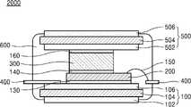
먼저, 도 4를 참조하면, 본 발명의 비교예에 따른 양면 냉각 파워 모듈(2000)은 하나의 모듈에 대해서 개별적으로 부품을 쌓아 올리는 방식으로 제조한다. 도 4에 도시된 구조도는 도 3에 도시된 평면도에서 CC를 기준으로 절단한 단면을 의미한다. 도 3에서 Al 와이어(150) 및 전력소자 칩(200)의 배치여부를 설명하기 위해서 상부 DBC 기판(500)은 생략되었으나, 도 4의 구조도에서는 적층 구조를 설명하기 위해서 상부 DBC 기판(500)을 적층한 형태로 구성하였다.First, referring to FIG. 4 , the double-sided
복수개의 전력소자 칩(200)을 Al 와이어(150)를 이용하여 단자(400)들과 연결한다. 이 때문에 Al 와이어 본딩의 높이 제한으로 인해 전력 모듈의 두께를 낮게 제어하기가 매우 어렵다. 또, 동일한 정격의 IGBT 대비 SiC 전력소자 칩(200)은 축소된 칩 면적으로 인해 열이 분산되지 못하고 국부적인 부분에 집중된다. 이에 따라 칩의 불량 발생률이 증가하게 되고, 생산성의 저하를 가져오는 문제점을 갖고 있다.The plurality of
이를 해결하기 위해서, 본 발명에서는 Al 와이어를 이용하지 않고, 전력소자 칩을 실장함으로써, 냉각 효율은 증가시키고, 생산성을 향상시킬 수 있는 양면 냉각 파워 모듈의 제조방법을 제공하고자 한다.In order to solve this problem, the present invention intends to provide a method of manufacturing a double-sided cooling power module capable of increasing cooling efficiency and improving productivity by mounting a power device chip without using an Al wire.
도 1 및 도 2는 본 발명의 일 실시예에 따른 양면 냉각 파워 모듈을 보여주는 개략적으로 도해하는 평면도이다.1 and 2 are plan views schematically illustrating a double-sided cooling power module according to an embodiment of the present invention.
도 1 및 도 2를 참조하면, 본 발명의 일 실시예에 따른 양면 냉각 파워 모듈(1000)은 하부 DBC 기판(100), 전력소자 칩(200), 스페이서(300) 및 상부 DBC 기판(500)이 순차적으로 적층된 형태의 구조를 포함할 수 있다. 구체적으로, 도 1은 하부 DBC 기판(100) 상에 전력소자 칩(200)까지 형성된 양면 냉각 파워 모듈의 하부 구조체(1000A)를 의미하고, 도 2는 스페이서(300) 및 상부 DBC 기판(500)이 형성된 양면 냉각 파워 모듈의 상부 구조체(1000B)를 의미한다.1 and 2 , the double-sided
하부 구조체(1000A)를 먼저 살펴보면, 하부 DBC 기판(100) 상에 전력소자 칩(200)이 배치된다. 전력소자 칩(200)은 TSV(Through Silicon Via) 기판(212)에 형성된 금속 배선(미도시)에 복수개의 전력소자(220)가 병렬로 접합된 구조를 포함한다. 여기서, 하부 DBC(direct bonder copper) 기판(100)이라는 용어는 AMC(active metal brazed copper) 기판을 의미하기도 한다. 하부 DBC 기판(100)은 구리(Cu)와 같은 전도성이 좋은 금속층(102, 106)이 세라믹 기판(104)의 상부면 및 하부면 상에 형성된 것으로서, 적어도 하나 이상의 층이 적층된 형태로 형성될 수 있다.Looking at the
하부 DBC 기판(100)은 제 1 하부 금속층(102), 제 1 세라믹층(104) 및 제 1 상부 금속층(106)을 포함할 수 있다. 제 1 세라믹 기판(104)의 하부면과 상부면 각각에 제 1 하부 금속층(102)과 제 1 상부 금속층(106)이 형성될 수 있다. 여기서, 제 1 하부 금속층(102)과 제 1 상부 금속층(106)은 금속회로패턴으로 이해될 수 있다.The
또한, 하부 DBC 기판(100)의 일단 및 타단에는 리드프레임으로 구성된 여러 단자(400)들이 형성된다. 예를 들어, 하부 DBC 기판(100)의 일단에 형성된 단자(400)는 시그널 단자를 의미하고, 타단에 형성된 단자(400)는 파워 단자를 의미한다.In addition,
전력소자 칩(200)이 형성되지 않은 영역에는 상부 DBC 기판(500)을 형성할 때, 빈 공간으로 형성되기 때문에 스페이서(300)가 형성되어 안정적인 구조체가 형성되도록 단자(400)들만 형성된다.When the
한편, 상부 구조체(1000B)는 하부 구조체(1000A)의 상면에 적층되는 형태로서, 동일한 크기의 상부 DBC 기판(500)이 배치된다. 상부 DBC 기판(500)은 하부 DBC 기판(100)과 동일한 것을 사용한다. 또, 전력소자 칩(200)이 배치된 영역에 걸쳐서 단층 형태의 스페이서(300)가 상부 구조체(1000B)의 하부면에 접합될 수 있다. 상부 DBC 기판(500)의 금속 패턴은 하부 구조체(1000A)에 배치된 전력소자 칩(200)의 전기적 연결을 고려하여 설계된다.Meanwhile, the
이하에서, 도 5 내지 도 12를 참조하여 양면 냉각 파워 모듈의 제조방법에 대해서 구체적으로 설명하면서, 각 구성요소들의 유기적 결합 관계에 대해서 상세하게 후술하고자 한다.Hereinafter, a method of manufacturing a double-sided cooling power module will be described in detail with reference to FIGS. 5 to 12 , and an organic coupling relationship of each component will be described in detail later.
도 5 내지 도 12는 본 발명의 일 실시예에 따른 양면 냉각 파워의 제조방법을 공정순서에 맞게 개략적으로 도해하는 도면들이다. 도 5 내지 도 12에 도시된 도면은 도 1에 도시된 도면에서 일점 쇄선으로 구분된 영역(CC)을 기준으로 절단한 단면도이다.5 to 12 are diagrams schematically illustrating a method of manufacturing a double-sided cooling power according to a process sequence according to an embodiment of the present invention. The drawings shown in FIGS. 5 to 12 are cross-sectional views taken based on the area CC divided by the dashed-dotted line in the drawing shown in FIG. 1 .
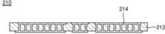
도 5 내지 도 7을 참조하면, 먼저, TSV 기판(210)을 준비할 수 있다. TSV(Through Silicon Via) 기판(210)은 비아(via)를 구비하는 기판(212)의 일부에 금속 배선(214)을 형성한 것을 포함한다.5 to 7 , first, a
기판(212)은 예를 들어, Si 기판을 이용하며, Si 기판을 수직관통하는 비아(via)에 배선 공정을 이용하여 금속 배선(214)이 매립된 형태로 형성된 TSV 기판(210)을 형성한다. TSV 기판(210)은 이미 공지된 기술이므로 이에 대한 상세한 설명은 생략한다. TSV 기판(210)의 일면과 타면에는 각각 금속 배선(214)이 형성되어 전력소자 칩(200)으로부터 소스 신호와 게이트 신호를 받아 기판(212)을 관통하는 비아를 통해 하부로 전달할 수 있게 된다. 여기서, Si 기판을 예로 들어서 설명하였으나, Si 기판 대신 Glass와 같은 무기질 계열의 재료를 기판으로 사용할 수도 있다.The
준비된 TSV 기판(210) 상에 복수개의 전력소자(220)들을 형성한다. 이때, 복수개의 전력소자(220)들은 플립칩의 형태로 형성된다. 예를 들어, 솔더(230)를 이용하여 TSV 기판(210)에 구비된 금속 배선(214)에 전기적으로 접속되어 복수개의 전력소자(220)가 TSV 기판(210) 상에 병렬로 접합된다. 여기서, 솔더(230)는 접합층으로 존재하게 된다. 솔더(230)는 복수개의 전력소자(220)의 전극부, 즉, 게이트 전극부 및 소스 전극부에 형성되어 TSV 기판(210)과 전기적으로 연결된다.A plurality of
이후에, 복수개의 전력소자(220) 및 TSV 기판(210) 사이에 존재하는 간극에 충진제(240)를 충진한 후 이를 경화시켜 전력소자(220)를 TSV 기판(210) 상에 고정할 수 있다. 여기서, 전력소자(220)는 예를 들어, SiC 칩을 의미하며, 이외에도 소형의 칩(chip)들을 접합할 수도 있다. 이렇게 본 발명에서는 Si 기판에 비아를 가공한 후 금속층으로 충진된 기판 위에 복수개의 SiC 칩들을 하나의 패키지 구조로 제조하여 인덕턴스 값을 낮게 제어할 수 있다.Thereafter, a
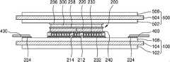
도 8을 참조하면, 준비된 하부 DBC 기판(100) 상에 제조된 전력소자 칩(200)을 형성할 수 있다. 하부 DBC 기판(100)은 제 1 하부 금속층(102), 제 1 세라믹층(104) 및 제 1 상부 금속층(106)으로 구성된다. 여기서, 전력소자 칩(200)이 실장될 수 있도록 제 1 상부 금속층(106)은 금속회로패턴이 형성된다. 제 1 상부 금속층(106)과 전력소자 칩(200) 사이에는 솔더(232)를 개재하여 솔더링함으로써 하부 DBC 기판(100) 상에 도 7에 도시된 전력소자 칩(200)을 접합할 수 있다. 여기서, 솔더(232)를 이용하여 설명하였으나, 하부 DBC 기판(100) 상에 소결 접합용 페이스트 또는 필름을 도포한 후 SiC 소자가 접합된 Si 기판을 접합할 수도 있다.Referring to FIG. 8 , the manufactured
도 9를 참조하면, 하부 DBC 기판(100)의 일단과 타단에 시그널 단자(400) 및 파워 단자(400)를 각각 형성할 수 있다. 도면에는 하부 DBC 기판(100) 상에 전력소자 칩(200)을 형성한 이후에 단자들을 형성한 것으로 도시하였으나, 공정의 편의상 전력소자 칩(200)과 동시에 형성할 수도 있고, 혹은 그 이전에 단자들을 형성할 수도 있다.Referring to FIG. 9 , a
단자(400)는 리드프레임을 이용하여 형성하며, 하부 DBC 기판(100)과 일체형으로 가공하여 몰딩한 후 후공정을 통해서 리드 단자를 형성할 수 있다. 또는 도면에 도시된 바와 같이, 솔더(234)를 이용하여 하부 DBC 기판(100)의 양단에 각각 형성할 수 있다. 리드프레임 단자를 가공하는 공정은 이미 기공지된 것으로서, 이에 대한 상세한 설명은 생략한다.The terminal 400 is formed using a lead frame, and after processing and molding integrally with the
도 10을 참조하면, 준비된 상부 DBC 기판(500)의 일면 상에 스페이서(300)를 형성할 수 있다. 상부 DBC 기판(500)은 하부 DBC 기판(100)과 동일하게 제 2 하부 금속층(502), 제 2 세라믹층(504) 및 제 2 상부 금속층(506)으로 구성된다.Referring to FIG. 10 , a
스페이서(300)는 상부 DBC 기판(500)의 제 2 하부 금속층(502)이 형성된 일면 상에 형성될 수 있다. 스페이서(300)는 열팽창계수(CTE)가 낮은 재료를 사용할 수 있다. 예를 들어, 스페이서(300)는 전력소자 칩(200)의 상부 또는 하부로 전기적 신호 및 방열을 수행하고, 예를 들어, 구리(Cu)와 같은 전도성이 우수한 금속을 블럭으로 사용할 수 있다.The
스페이서(300)는 전력소자 칩(200)의 형성방법과 동일하게, 스페이서(300)와 상부 DBC 기판(500) 사이에 솔더(236)를 개재하여 솔더링한다. 스페이서(300)도 전력소자 칩(200)과 접합될 영역에 소결 접합용 페이스트 또는 필름을 도포한 후 소결접합 할 수 있다.The
도 11을 참조하면, 도 10에 도시된 스페이서(300)가 접합된 상부 DBC 기판(500)을 전력소자 칩(200) 상에 형성할 수 있다. 이때, 전력소자 칩(200) 상에 스페이서(300)가 맞닿도록 상부 DBC 기판(500)을 뒤집어서 전력소자 칩(200)과 접합한다. 여기서, 전력소자 칩(200)과 스페이서(300) 사이에 솔더(238)를 개재하여 솔더링한다.Referring to FIG. 11 , the
도 12를 참조하면, 상부 DBC 기판(500)이 전력소자 칩(200) 상에 형성된 이후에 하부 DBC 기판(100) 및 상부 DBC 기판(500)의 외주면을 감싸도록 몰딩부(600)를 형성한다. 몰딩부(600)는 내부에 포함된 구성요소들을 보호하는 기능을 수행하며, 리드프레임으로 제조된 단자(400)의 적어도 어느 일부는 몰딩부(600)의 외부로 돌출된다. 몰딩부(600)는 예를 들어, 에폭시몰딩컴파운드(EMC) 또는 폴리이미드(poly imide) 계열의 재료와 같이, 절연성 및 보호성이 우수한 폴리머 재질을 사용할 수 있다. 몰딩부(600)에 의해서 전력소자 칩(200) 및 스페이서(300)는 모두 매립된다.Referring to FIG. 12 , after the
상술한 바와 같이, 병렬로 복수개의 전력소자 칩이 와이어 본딩 방식이 아닌, 대면적의 메탈 패턴(스페이서)에 의해 전류가 이동하는 구조로서 인덕턴스의 값을 낮춰줄 수 있다. 전력소자 칩으로부터 방열판까지의 거리 및 접합층을 줄여주기 때문에 열저항이 감소될 수 있다. 또, 모듈의 상부에서 열이 빠져나갈 수 있는 구조를 가지기 때문에 양면으로 방열이 가능하다.As described above, a plurality of power device chips in parallel have a structure in which current moves by a large-area metal pattern (spacer) rather than a wire bonding method, and thus the value of inductance can be lowered. Since the distance from the power device chip to the heat sink and the bonding layer are reduced, thermal resistance may be reduced. In addition, since it has a structure that allows heat to escape from the upper part of the module, it is possible to dissipate heat from both sides.
한편, 칩에서 발생되는 열을 절연 기판으로 보내기 전에 열팽창계수(CTE)가 유사한 층을 추가하여 열 전달면적을 확대시켜 주어 열변형에서 오는 스트레스를 중간의 Si 기판 및 메탈 블록이 감소시켜 칩의 내구성 및 신뢰성을 향상시켜줄 수 있다.On the other hand, before the heat generated from the chip is sent to the insulating substrate, a layer with a similar coefficient of thermal expansion (CTE) is added to expand the heat transfer area. and reliability.
본 발명은 도면에 도시된 실시예를 참고로 설명되었으나 이는 예시적인 것에 불과하며, 당해 기술분야에서 통상의 지식을 가진 자라면 이로부터 다양한 변형 및 균등한 다른 실시예가 가능하다는 점을 이해할 것이다. 따라서 본 발명의 진정한 기술적 보호 범위는 첨부된 특허청구범위의 기술적 사상에 의하여 정해져야 할 것이다.Although the present invention has been described with reference to the embodiment shown in the drawings, which is only exemplary, those skilled in the art will understand that various modifications and equivalent other embodiments are possible therefrom. Therefore, the true technical protection scope of the present invention should be determined by the technical spirit of the appended claims.
100: 하부 DBC 기판
102: 제 1 하부 금속층
104: 제 1 세라믹층
106: 제 1 상부 금속층
150: 와이어
130, 140, 160, 230, 232, 234, 236, 238: 솔더
200: 전력소자 칩
210: TSV 기판
212: 기판
214: 금속 배선
220: 전력소자
240: 충진제
300: 스페이서
400: 단자
500: 상부 DBC 기판
502: 제 2 하부 금속층
504: 제 2 세라믹층
506: 제 2 상부 금속층
600: 몰딩부
1000, 2000: 양면 냉각 파워 모듈100: lower DBC substrate
102: first lower metal layer
104: first ceramic layer
106: first upper metal layer
150: wire
130, 140, 160, 230, 232, 234, 236, 238: Solder
200: power device chip
210: TSV substrate
212: substrate
214: metal wiring
220: power device
240: filler
300: spacer
400: terminal
500: upper DBC substrate
502: second lower metal layer
504: second ceramic layer
506: second upper metal layer
600: molding unit
1000, 2000: double-sided cooling power module
Claims (14)
Translated fromKorean상기 하부 DBC 기판 상에 형성된 전력소자 칩;
상기 하부 DBC 기판 상에 형성된 외부 연결 단자;
상기 전력소자 칩 상에 형성된 스페이서; 및
상기 스페이서 상에 형성된 상부 DBC 기판;을 포함하고,
상기 전력소자 칩은,
상기 하부 DBC 기판 상에 접합되어 상기 하부 DBC 기판을 통해 상기 외부 연결 단자와 전기적으로 연결되는 TSV 기판; 및
상기 TSV 기판 상에 병렬로 접합되는 복수개의 전력소자를 포함하는,
양면 냉각 파워 모듈.lower DBC substrate;
a power device chip formed on the lower DBC substrate;
an external connection terminal formed on the lower DBC substrate;
a spacer formed on the power device chip; and
an upper DBC substrate formed on the spacer; and
The power device chip,
a TSV substrate bonded to the lower DBC substrate and electrically connected to the external connection terminal through the lower DBC substrate; and
Comprising a plurality of power devices bonded in parallel on the TSV substrate,
Double-sided cooling power module.
상기 복수개의 전력소자의 전극부는 상기 TSV 기판 상에 접합층을 이용하여 접합된,
양면 냉각 파워 모듈.The method of claim 1,
The electrode portions of the plurality of power devices are bonded using a bonding layer on the TSV substrate,
Double-sided cooling power module.
상기 복수개의 전력소자 및 상기 TSV 기판 사이에 존재하는 간극은 충진제로 충진된,
양면 냉각 파워 모듈.The method of claim 1,
A gap existing between the plurality of power devices and the TSV substrate is filled with a filler,
Double-sided cooling power module.
상기 하부 DBC 기판의 적어도 어느 일단과 타단에 각각 형성된 시그널 단자 및 파워 단자를 포함하는,
양면 냉각 파워 모듈.The method of claim 1, wherein the external connection terminal is
including a signal terminal and a power terminal respectively formed on at least one end and the other end of the lower DBC substrate,
Double-sided cooling power module.
상기 시그널 단자 및 파워 단자는 상기 하부 DBC 기판 상에 접합층을 이용하여 접합된,
양면 냉각 파워 모듈.5. The method of claim 4,
The signal terminal and the power terminal are bonded using a bonding layer on the lower DBC substrate,
Double-sided cooling power module.
상기 스페이서는 상기 복수개의 전력소자 상에 단층으로 형성된,
양면 냉각 파워 모듈.The method of claim 1,
The spacer is formed as a single layer on the plurality of power devices,
Double-sided cooling power module.
상기 하부 DBC 기판 및 상기 상부 DBC 기판의 외주면을 감싸도록 형성된 몰딩부;를 포함하고, 상기 시그널 단자 및 파워 단자의 적어도 어느 일부는 상기 몰딩부의 외부로 돌출된,
양면 냉각 파워 모듈.5. The method of claim 4,
a molding part formed to surround outer peripheral surfaces of the lower DBC substrate and the upper DBC substrate, wherein at least some of the signal terminal and the power terminal protrude to the outside of the molding part,
Double-sided cooling power module.
상기 전력소자 칩 및 상기 스페이서는 상기 몰딩부에 의해 매립된,
양면 냉각 파워 모듈.8. The method of claim 7,
The power device chip and the spacer are buried by the molding part,
Double-sided cooling power module.
TSV(Through Silicon Via) 기판 상에 복수개의 전력소자를 병렬로 접합하여 전력소자 칩을 형성하는 단계;
상기 하부 DBC 기판 상에 외부 연결 단자와 상기 전력소자 칩을 형성하되, 상기 외부 연결 단자와 상기 전력소자 칩은 상기 하부 DBC 기판을 통해 전기적으로 연결되도록 하는 단계;
상기 상부 DBC 기판의 어느 일면 상에 스페이서를 형성하는 단계; 및
상기 전력소자 칩 상에 상기 스페이서가 맞닿도록 상기 상부 DBC 기판을 상기 전력소자 칩 상에 형성하는 단계;를 포함하는,
양면 냉각 파워 모듈의 제조방법.preparing a lower DBC substrate and an upper DBC substrate;
forming a power device chip by bonding a plurality of power devices in parallel on a TSV (Through Silicon Via) substrate;
forming an external connection terminal and the power device chip on the lower DBC substrate, wherein the external connection terminal and the power device chip are electrically connected through the lower DBC substrate;
forming a spacer on any one surface of the upper DBC substrate; and
Forming the upper DBC substrate on the power device chip so that the spacer abuts on the power device chip;
A method for manufacturing a double-sided cooling power module.
상기 전력소자 칩을 형성하는 단계는,
상기 복수개의 전력소자의 전극부가 상기 TSV 기판과 전기적으로 연결되도록, 상기 복수개의 전력소자의 전극부가 접합층을 이용하여 상기 TSV 기판 상에 접합되는 단계를 포함하는,
양면 냉각 파워 모듈의 제조방법.10. The method of claim 9,
The step of forming the power device chip,
and bonding the electrode parts of the plurality of power devices on the TSV substrate using a bonding layer so that the electrode parts of the plurality of power devices are electrically connected to the TSV substrate.
A method for manufacturing a double-sided cooling power module.
상기 전력소자 칩을 형성하는 단계는,
상기 복수개의 전력소자 및 상기 TSV 기판 사이에 존재하는 간극에 충진제를 충진하는 단계를 포함하는,
양면 냉각 파워 모듈의 제조방법.10. The method of claim 9,
The step of forming the power device chip,
Comprising the step of filling the gap existing between the plurality of power devices and the TSV substrate, a filler,
A method for manufacturing a double-sided cooling power module.
상기 하부 DBC 기판의 적어도 어느 일단과 타단에 시그널 단자 및 파워 단자를 각각 형성하는 것을 포함하는,
양면 냉각 파워 모듈의 제조방법.10. The method of claim 9, wherein the formation of the external connection terminal
Comprising forming a signal terminal and a power terminal on at least one end and the other end of the lower DBC board, respectively,
A method for manufacturing a double-sided cooling power module.
상기 상부 DBC 기판을 상기 전력소자 칩 상에 형성하는 단계 이후에,
상기 시그널 단자 및 파워 단자의 적어도 어느 일부가 몰딩부의 외부로 돌출되도록, 상기 하부 DBC 기판 및 상기 상부 DBC 기판의 외주면을 감싸도록 상기 몰딩부를 형성하는 단계를 포함하는,
양면 냉각 파워 모듈의 제조방법.13. The method of claim 12,
After forming the upper DBC substrate on the power device chip,
forming the molding part to surround outer peripheral surfaces of the lower DBC substrate and the upper DBC substrate so that at least any part of the signal terminal and the power terminal protrude outside the molding part;
A method for manufacturing a double-sided cooling power module.
상기 몰딩부에 의해서 상기 전력소자 칩 및 상기 스페이서가 매립되는,
양면 냉각 파워 모듈의 제조방법.14. The method of claim 13,
The power device chip and the spacer are buried by the molding part,
A method for manufacturing a double-sided cooling power module.
Priority Applications (1)
| Application Number | Priority Date | Filing Date | Title |
|---|---|---|---|
| KR1020200172748AKR102464477B1 (en) | 2020-12-10 | 2020-12-10 | Dual side cooling power module and manufacturing method of the same |
Applications Claiming Priority (1)
| Application Number | Priority Date | Filing Date | Title |
|---|---|---|---|
| KR1020200172748AKR102464477B1 (en) | 2020-12-10 | 2020-12-10 | Dual side cooling power module and manufacturing method of the same |
Publications (2)
| Publication Number | Publication Date |
|---|---|
| KR20220082655A KR20220082655A (en) | 2022-06-17 |
| KR102464477B1true KR102464477B1 (en) | 2022-11-09 |
Family
ID=82269081
Family Applications (1)
| Application Number | Title | Priority Date | Filing Date |
|---|---|---|---|
| KR1020200172748AActiveKR102464477B1 (en) | 2020-12-10 | 2020-12-10 | Dual side cooling power module and manufacturing method of the same |
Country Status (1)
| Country | Link |
|---|---|
| KR (1) | KR102464477B1 (en) |
Families Citing this family (2)
| Publication number | Priority date | Publication date | Assignee | Title |
|---|---|---|---|---|
| CN115172272A (en)* | 2022-07-29 | 2022-10-11 | 武汉新芯集成电路制造有限公司 | High-aspect-ratio TSV (through silicon via) electric communication structure and manufacturing method thereof |
| CN120356875B (en)* | 2025-06-25 | 2025-09-30 | 浙江大学 | Embedded double-sided direct cooling power module structure based on metal core composite substrate |
Citations (1)
| Publication number | Priority date | Publication date | Assignee | Title |
|---|---|---|---|---|
| KR101755769B1 (en) | 2014-10-29 | 2017-07-07 | 현대자동차주식회사 | Dual side cooling power module and Method for manufacturing the same |
Family Cites Families (3)
| Publication number | Priority date | Publication date | Assignee | Title |
|---|---|---|---|---|
| KR100723454B1 (en)* | 2004-08-21 | 2007-05-30 | 페어차일드코리아반도체 주식회사 | Power module package with high heat dissipation capacity and its manufacturing method |
| KR101977956B1 (en)* | 2017-06-21 | 2019-05-13 | 현대오트론 주식회사 | Manufacturing method of power semiconductor module |
| KR20200071596A (en)* | 2018-12-11 | 2020-06-19 | 현대자동차주식회사 | Method of controlling height of double-sided cooling power module |
- 2020
- 2020-12-10KRKR1020200172748Apatent/KR102464477B1/enactiveActive
Patent Citations (1)
| Publication number | Priority date | Publication date | Assignee | Title |
|---|---|---|---|---|
| KR101755769B1 (en) | 2014-10-29 | 2017-07-07 | 현대자동차주식회사 | Dual side cooling power module and Method for manufacturing the same |
Also Published As
| Publication number | Publication date |
|---|---|
| KR20220082655A (en) | 2022-06-17 |
Similar Documents
| Publication | Publication Date | Title |
|---|---|---|
| JP6300978B2 (en) | Power semiconductor module | |
| US8890310B2 (en) | Power module package having excellent heat sink emission capability and method for manufacturing the same | |
| US10818574B2 (en) | Plug-in type power module and subsystem thereof | |
| US20100134979A1 (en) | Power semiconductor apparatus | |
| JP7691208B2 (en) | Power module and manufacturing method thereof, converter, and electronic device | |
| KR102163662B1 (en) | Dual side cooling power module and manufacturing method of the same | |
| KR102800218B1 (en) | Inverter power module | |
| KR102490612B1 (en) | Power semiconductor module | |
| WO2015016017A1 (en) | Semiconductor device | |
| KR102464477B1 (en) | Dual side cooling power module and manufacturing method of the same | |
| US20180040562A1 (en) | Elektronisches modul und verfahren zu seiner herstellung | |
| US20240321692A1 (en) | Power module | |
| US12068298B2 (en) | High power density 3D semiconductor module packaging | |
| KR102683179B1 (en) | Dual side cooling power module and manufacturing method of the same | |
| EP4340017B1 (en) | Packaging device, packaging module, and electronic device | |
| JP7520273B1 (en) | Power Module | |
| US20250233032A1 (en) | Double-sided cooling semiconductor device | |
| US20240213126A1 (en) | Semiconductor device | |
| KR20240109845A (en) | Dual side cooling power module and manufacturing method of the same | |
| KR20240135290A (en) | Dual side cooling power module | |
| KR20230136459A (en) | Power semiconductor module and method for manufacturing thereof | |
| KR20240123179A (en) | Dual side cooling power module | |
| CN117293118A (en) | Power module and manufacturing method thereof | |
| TW202402111A (en) | Power module and method for manufacturing the same | |
| CN119547209A (en) | Circuit assembly having two circuit carriers and a semiconductor component |
Legal Events
| Date | Code | Title | Description |
|---|---|---|---|
| PA0109 | Patent application | Patent event code:PA01091R01D Comment text:Patent Application Patent event date:20201210 | |
| PA0201 | Request for examination | ||
| PN2301 | Change of applicant | Patent event date:20210222 Comment text:Notification of Change of Applicant Patent event code:PN23011R01D | |
| PE0902 | Notice of grounds for rejection | Comment text:Notification of reason for refusal Patent event date:20220412 Patent event code:PE09021S01D | |
| PG1501 | Laying open of application | ||
| E701 | Decision to grant or registration of patent right | ||
| PE0701 | Decision of registration | Patent event code:PE07011S01D Comment text:Decision to Grant Registration Patent event date:20221027 | |
| PR0701 | Registration of establishment | Comment text:Registration of Establishment Patent event date:20221102 Patent event code:PR07011E01D | |
| PR1002 | Payment of registration fee | Payment date:20221103 End annual number:3 Start annual number:1 | |
| PG1601 | Publication of registration |