KR102461388B1 - Scan Driver and Display Device Using the same - Google Patents
Scan Driver and Display Device Using the sameDownload PDFInfo
- Publication number
- KR102461388B1 KR102461388B1KR1020150191823AKR20150191823AKR102461388B1KR 102461388 B1KR102461388 B1KR 102461388B1KR 1020150191823 AKR1020150191823 AKR 1020150191823AKR 20150191823 AKR20150191823 AKR 20150191823AKR 102461388 B1KR102461388 B1KR 102461388B1
- Authority
- KR
- South Korea
- Prior art keywords
- gate
- clock signal
- switch
- response
- signal
- Prior art date
- Legal status (The legal status is an assumption and is not a legal conclusion. Google has not performed a legal analysis and makes no representation as to the accuracy of the status listed.)
- Active
Links
Images


Classifications
- G—PHYSICS
- G09—EDUCATION; CRYPTOGRAPHY; DISPLAY; ADVERTISING; SEALS
- G09G—ARRANGEMENTS OR CIRCUITS FOR CONTROL OF INDICATING DEVICES USING STATIC MEANS TO PRESENT VARIABLE INFORMATION
- G09G3/00—Control arrangements or circuits, of interest only in connection with visual indicators other than cathode-ray tubes
- G09G3/20—Control arrangements or circuits, of interest only in connection with visual indicators other than cathode-ray tubes for presentation of an assembly of a number of characters, e.g. a page, by composing the assembly by combination of individual elements arranged in a matrix no fixed position being assigned to or needed to be assigned to the individual characters or partial characters
- G09G3/22—Control arrangements or circuits, of interest only in connection with visual indicators other than cathode-ray tubes for presentation of an assembly of a number of characters, e.g. a page, by composing the assembly by combination of individual elements arranged in a matrix no fixed position being assigned to or needed to be assigned to the individual characters or partial characters using controlled light sources
- G09G3/30—Control arrangements or circuits, of interest only in connection with visual indicators other than cathode-ray tubes for presentation of an assembly of a number of characters, e.g. a page, by composing the assembly by combination of individual elements arranged in a matrix no fixed position being assigned to or needed to be assigned to the individual characters or partial characters using controlled light sources using electroluminescent panels
- G09G3/32—Control arrangements or circuits, of interest only in connection with visual indicators other than cathode-ray tubes for presentation of an assembly of a number of characters, e.g. a page, by composing the assembly by combination of individual elements arranged in a matrix no fixed position being assigned to or needed to be assigned to the individual characters or partial characters using controlled light sources using electroluminescent panels semiconductive, e.g. using light-emitting diodes [LED]
- G09G3/3208—Control arrangements or circuits, of interest only in connection with visual indicators other than cathode-ray tubes for presentation of an assembly of a number of characters, e.g. a page, by composing the assembly by combination of individual elements arranged in a matrix no fixed position being assigned to or needed to be assigned to the individual characters or partial characters using controlled light sources using electroluminescent panels semiconductive, e.g. using light-emitting diodes [LED] organic, e.g. using organic light-emitting diodes [OLED]
- G09G3/3266—Details of drivers for scan electrodes
- G—PHYSICS
- G09—EDUCATION; CRYPTOGRAPHY; DISPLAY; ADVERTISING; SEALS
- G09G—ARRANGEMENTS OR CIRCUITS FOR CONTROL OF INDICATING DEVICES USING STATIC MEANS TO PRESENT VARIABLE INFORMATION
- G09G3/00—Control arrangements or circuits, of interest only in connection with visual indicators other than cathode-ray tubes
- G09G3/20—Control arrangements or circuits, of interest only in connection with visual indicators other than cathode-ray tubes for presentation of an assembly of a number of characters, e.g. a page, by composing the assembly by combination of individual elements arranged in a matrix no fixed position being assigned to or needed to be assigned to the individual characters or partial characters
- G09G3/34—Control arrangements or circuits, of interest only in connection with visual indicators other than cathode-ray tubes for presentation of an assembly of a number of characters, e.g. a page, by composing the assembly by combination of individual elements arranged in a matrix no fixed position being assigned to or needed to be assigned to the individual characters or partial characters by control of light from an independent source
- G09G3/36—Control arrangements or circuits, of interest only in connection with visual indicators other than cathode-ray tubes for presentation of an assembly of a number of characters, e.g. a page, by composing the assembly by combination of individual elements arranged in a matrix no fixed position being assigned to or needed to be assigned to the individual characters or partial characters by control of light from an independent source using liquid crystals
- G09G3/3611—Control of matrices with row and column drivers
- G09G3/3674—Details of drivers for scan electrodes
- G09G3/3677—Details of drivers for scan electrodes suitable for active matrices only
- G—PHYSICS
- G09—EDUCATION; CRYPTOGRAPHY; DISPLAY; ADVERTISING; SEALS
- G09G—ARRANGEMENTS OR CIRCUITS FOR CONTROL OF INDICATING DEVICES USING STATIC MEANS TO PRESENT VARIABLE INFORMATION
- G09G2230/00—Details of flat display driving waveforms
- G—PHYSICS
- G09—EDUCATION; CRYPTOGRAPHY; DISPLAY; ADVERTISING; SEALS
- G09G—ARRANGEMENTS OR CIRCUITS FOR CONTROL OF INDICATING DEVICES USING STATIC MEANS TO PRESENT VARIABLE INFORMATION
- G09G2310/00—Command of the display device
- G09G2310/02—Addressing, scanning or driving the display screen or processing steps related thereto
- G09G2310/0264—Details of driving circuits
- G09G2310/0286—Details of a shift registers arranged for use in a driving circuit
- G—PHYSICS
- G09—EDUCATION; CRYPTOGRAPHY; DISPLAY; ADVERTISING; SEALS
- G09G—ARRANGEMENTS OR CIRCUITS FOR CONTROL OF INDICATING DEVICES USING STATIC MEANS TO PRESENT VARIABLE INFORMATION
- G09G2310/00—Command of the display device
- G09G2310/02—Addressing, scanning or driving the display screen or processing steps related thereto
- G09G2310/0264—Details of driving circuits
- G09G2310/0289—Details of voltage level shifters arranged for use in a driving circuit
- G—PHYSICS
- G09—EDUCATION; CRYPTOGRAPHY; DISPLAY; ADVERTISING; SEALS
- G09G—ARRANGEMENTS OR CIRCUITS FOR CONTROL OF INDICATING DEVICES USING STATIC MEANS TO PRESENT VARIABLE INFORMATION
- G09G2330/00—Aspects of power supply; Aspects of display protection and defect management
- G09G2330/02—Details of power systems and of start or stop of display operation
- G09G2330/021—Power management, e.g. power saving
Landscapes
- Engineering & Computer Science (AREA)
- Physics & Mathematics (AREA)
- Computer Hardware Design (AREA)
- General Physics & Mathematics (AREA)
- Theoretical Computer Science (AREA)
- Chemical & Material Sciences (AREA)
- Crystallography & Structural Chemistry (AREA)
- Control Of Indicators Other Than Cathode Ray Tubes (AREA)
Abstract
Translated fromKoreanDescription
Translated fromKorean본 발명은 게이트 구동부 및 이를 이용한 표시장치에 관한 것이다.The present invention relates to a gate driver and a display device using the same.
정보화 기술이 발달함에 따라 사용자와 정보간의 연결 매체인 표시장치의 시장이 커지고 있다. 이에 따라, 유기전계발광표시장치(Organic Light Emitting Display: OLED), 액정표시장치(Liquid Crystal Display: LCD) 및 플라즈마표시장치(Plasma Display Panel: PDP) 등과 같은 표시장치의 사용이 증가하고 있다.As information technology develops, the market for display devices, which is a connection medium between users and information, is growing. Accordingly, the use of display devices such as an organic light emitting display (OLED), a liquid crystal display (LCD), and a plasma display panel (PDP) is increasing.
앞서 설명한 표시장치 중 일부 예컨대, 액정표시장치나 유기전계발광표시장치는 표시패널에 포함된 서브 픽셀들에 게이트신호 및 데이터신호 등이 공급되면, 선택된 서브 픽셀이 발광을 하게 됨으로써 영상을 표시할 수 있다.In some of the above-described display devices, for example, a liquid crystal display device or an organic light emitting display device, when a gate signal and a data signal are supplied to sub-pixels included in a display panel, the selected sub-pixel emits light to display an image. have.
위와 같은 표시장치는 복수의 서브 픽셀을 포함하는 표시패널과 표시패널을 구동하는 구동부가 포함된다. 구동부에는 표시패널에 게이트신호(또는 스캔신호)를 공급하는 게이트 구동부 및 표시패널에 데이터신호를 공급하는 데이터 구동부 등이 포함된다.The display device as described above includes a display panel including a plurality of sub-pixels and a driving unit for driving the display panel. The driver includes a gate driver that supplies a gate signal (or a scan signal) to the display panel, and a data driver that supplies a data signal to the display panel.
게이트 구동부는 집적회로 형태뿐만 아니라 박막 트랜지스터 공정과 함께 게이트인패널(Gate In Panel; GIP) 방식으로 표시패널에 형성되는 표시패널 내장형으로 이루어지기도 한다.The gate driver may be of an integrated circuit type as well as a display panel built-in type which is formed on a display panel by a gate in panel (GIP) method together with a thin film transistor process.
표시장치는 장치의 소비전류를 절감 및 개선하기 위하여, 게이트신호를 구성하는 게이트 전압의 레벨을 가변하는 GPM(Gate Pulse Modulation) 기능을 사용한다. 그런데 종래에 제안된 게이트 변조 방식은 클록신호의 위상이 많아질 경우 게이트 구동부의 구동 안정성과 소비전류 절감 효과가 저하되는바 이의 개선이 요구된다.The display device uses a GPM (Gate Pulse Modulation) function of varying the level of the gate voltage constituting the gate signal in order to reduce and improve the current consumption of the device. However, in the conventionally proposed gate modulation method, when the phase of the clock signal increases, the driving stability of the gate driver and the effect of reducing current consumption are reduced, so improvement is required.
상술한 배경기술의 문제점을 해결하기 위한 본 발명은 게이트 구동부의 구동 안정성과 소비전류 절감 효과를 향상하고 더 나아가 표시패널의 화면 품위를 향상하는 것이다.The present invention for solving the problems of the background art described above is to improve the driving stability of the gate driver and the effect of reducing current consumption, and further improve the quality of the screen of the display panel.
상술한 과제 해결 수단으로 본 발명은 레벨 시프터 회로 및 시프트 레지스터 회로를 포함하는 게이트 구동부를 제공한다. 레벨 시프터 회로는 신호를 출력한다. 시프트 레지스터 회로는 레벨 시프터 회로로부터 출력된 신호를 기반으로 게이트신호를 시프트하여 출력하는 스테이지들로 이루어진다. 레벨 시프터 회로는 게이트하이전압과 게이트로우전압을 스위칭하며 게이트 클록신호들을 생성하는 클록신호 생성부와, 외부로부터 공급된 온 클록신호 및 오프 클록신호에 대응하여 클록신호 생성부로부터 출력되는 게이트 클록신호들의 라이징 에지와 폴링 에지 중 하나를 선택적으로 변조하는 게이트 펄스 변조부를 포함한다.As a means of solving the above problems, the present invention provides a gate driver including a level shifter circuit and a shift register circuit. The level shifter circuit outputs a signal. The shift register circuit includes stages that shift and output a gate signal based on a signal output from the level shifter circuit. The level shifter circuit includes a clock signal generator that switches a gate high voltage and a gate low voltage and generates gate clock signals, and a gate clock signal output from the clock signal generator in response to an on clock signal and an off clock signal supplied from the outside. and a gate pulse modulator for selectively modulating one of a rising edge and a falling edge of each of the plurality of gate pulse modulators.
게이트 펄스 변조부는 게이트 클록신호들의 라이징 에지와 폴링 에지 중 하나를 선택적으로 변조하기 위해, 온 클록신호 및 오프 클록신호에 대응하여 턴온 또는 턴오프 동작하며 자신의 외부전압단자로 전류 패스를 형성하거나 차단하는 제1스위치 및 제2스위치를 포함할 수 있다.In order to selectively modulate one of a rising edge and a falling edge of the gate clock signals, the gate pulse modulator turns on or turns off in response to the on clock signal and the off clock signal, and forms or blocks a current path through its external voltage terminal. It may include a first switch and a second switch.
삭제delete
게이트 펄스 변조부는 레벨 시프터 회로가 8상 이하의 게이트 클록신호를 형성할 경우, 게이트 클록신호의 라이징 에지 및 폴링 에지를 모두 사용하도록 제1스위치 및 제2스위치를 제어하고, 레벨 시프터 회로가 8상 이상의 게이트 클록신호를 형성할 경우, 게이트 클록신호의 라이징 에지 및 폴링 에지 중 하나만 사용하도록 제1스위치 및 제2스위치를 제어할 수 있다.The gate pulse modulator controls the first and second switches to use both the rising edge and the falling edge of the gate clock signal when the level shifter circuit forms a gate clock signal of 8 phases or less, and the level shifter circuit generates an 8 phase gate clock signal. When the above gate clock signal is formed, the first switch and the second switch may be controlled to use only one of the rising edge and the falling edge of the gate clock signal.
게이트 펄스 변조부는 외부 또는 내부로부터 공급된 게이트 펄스 제어신호에 대응하여 제1스위치 및 제2스위치 중 하나를 강제로 턴오프할 수 있다.The gate pulse modulator may forcibly turn off one of the first switch and the second switch in response to a gate pulse control signal supplied from the outside or the inside.
게이트 펄스 변조부는 온 클록신호의 폭과 오프 클록신호의 폭을 센싱하고 내부에 설정된 범위 내에 존재하면, 제1스위치 및 제2스위치 중 하나를 강제로 턴오프할 수 있다.The gate pulse modulator senses the width of the on-clock signal and the width of the off-clock signal, and when it exists within a range set therein, one of the first switch and the second switch may be forcibly turned off.
다른 측면에서 본 발명은 표시패널, 데이터 구동부 및 게이트 구동부를 포함하는 표시장치를 제공한다. 표시패널은 영상을 표시한다. 데이터 구동부는 표시패널에 데이터신호를 공급한다. 게이트 구동부는 표시패널에 게이트신호를 공급한다. 게이트 구동부는 레벨 시프터 회로와 레벨 시프터 회로로부터 출력된 신호를 기반으로 게이트신호를 시프트하여 출력하는 스테이지들로 이루어진 시프트 레지스터 회로를 포함한다. 레벨 시프터 회로는 게이트하이전압과 게이트로우전압을 스위칭하며 게이트 클록신호들을 생성하는 클록신호 생성부와, 외부로부터 공급된 온 클록신호 및 오프 클록신호에 대응하여 클록신호 생성부로부터 출력되는 게이트 클록신호들의 라이징 에지와 폴링 에지 중 하나를 선택적으로 변조한다.In another aspect, the present invention provides a display device including a display panel, a data driver, and a gate driver. The display panel displays an image. The data driver supplies a data signal to the display panel. The gate driver supplies a gate signal to the display panel. The gate driver includes a shift register circuit including a level shifter circuit and stages for shifting and outputting a gate signal based on a signal output from the level shifter circuit. The level shifter circuit includes a clock signal generator that switches a gate high voltage and a gate low voltage and generates gate clock signals, and a gate clock signal output from the clock signal generator in response to an on clock signal and an off clock signal supplied from the outside. Selectively modulate one of the rising edge and the falling edge.
게이트 펄스 변조부는 게이트 클록신호들의 라이징 에지와 폴링 에지 중 하나를 선택적으로 변조하기 위해, 온 클록신호 및 오프 클록신호에 대응하여 턴온 또는 턴오프 동작하며 자신의 외부전압단자로 전류 패스를 형성하거나 차단하는 제1스위치 및 제2스위치를 포함할 수 있다.In order to selectively modulate one of a rising edge and a falling edge of the gate clock signals, the gate pulse modulator turns on or turns off in response to the on clock signal and the off clock signal, and forms or blocks a current path through its external voltage terminal. It may include a first switch and a second switch.
게이트 펄스 변조부는 레벨 시프터 회로가 8상 이하의 게이트 클록신호를 형성할 경우, 게이트 클록신호의 라이징 에지 및 폴링 에지를 모두 사용하도록 제1스위치 및 상기 제2스위치를 제어하고, 레벨 시프터 회로가 8상 이상의 게이트 클록신호를 형성할 경우, 게이트 클록신호의 라이징 에지 및 폴링 에지 중 하나만 사용하도록 제1스위치 및 제2스위치를 제어할 수 있다.The gate pulse modulator controls the first switch and the second switch to use both the rising edge and the falling edge of the gate clock signal when the level shifter circuit forms a gate clock signal of 8 phases or less, and the level shifter circuit generates 8 phases. When forming the gate clock signal of more than one phase, the first switch and the second switch may be controlled to use only one of the rising edge and the falling edge of the gate clock signal.
삭제delete
본 발명은 게이트 클록신호에 원치 않는 이상 파형이 발생하는 문제를 해소하여 게이트 구동부의 구동 안정성을 향상하고 소비전류 절감 효과를 향상하고 더 나아가 표시패널의 화면 품위를 향상할 수 있는 효과가 있다.The present invention has the effect of improving the driving stability of the gate driver by solving the problem of generating an unwanted abnormal waveform in the gate clock signal, improving the effect of reducing current consumption, and further improving the screen quality of the display panel.
도 1은 표시장치의 개략적인 블록도.
도 2는 도 1에 도시된 서브 픽셀의 구성 예시도.
도 3은 본 발명의 제1실시예에 따른 레벨 시프터 회로의 개략적인 구성 예시도.
도 4는 도 3의 회로에 의한 게이트 펄스 변조의 일례를 나타낸 도면.
도 5는 실험예에 따른 레벨 시프터 회로의 클록신호 생성부를 개략적으로 나타낸 회로도.
도 6은 실험예의 문제점을 보여주는 파형도.
도 7은 본 발명의 제1실시예에 따른 레벨 시프터 회로의 클록신호 생성부를 개략적으로 나타낸 회로도.
도 8은 제1실시예의 개선점을 보여주는 파형도.
도 9는 본 발명의 제2실시예에 따른 레벨 시프터 회로의 개략적인 구성 예시도.
도 10은 본 발명의 제2실시예에 따른 레벨 시프터 회로의 클록신호 생성부를 개략적으로 나타낸 회로도.
도 11은 제2실시예의 개선점을 보여주는 파형도.1 is a schematic block diagram of a display device;
FIG. 2 is an exemplary configuration diagram of the sub-pixel shown in FIG. 1;
3 is a schematic configuration diagram of a level shifter circuit according to a first embodiment of the present invention;
Fig. 4 is a diagram showing an example of gate pulse modulation by the circuit of Fig. 3;
5 is a circuit diagram schematically showing a clock signal generator of a level shifter circuit according to an experimental example;
6 is a waveform diagram showing a problem in the experimental example.
7 is a circuit diagram schematically showing a clock signal generator of the level shifter circuit according to the first embodiment of the present invention.
Fig. 8 is a waveform diagram showing an improvement of the first embodiment;
9 is a schematic configuration diagram of a level shifter circuit according to a second embodiment of the present invention;
10 is a circuit diagram schematically showing a clock signal generator of a level shifter circuit according to a second embodiment of the present invention;
Fig. 11 is a waveform diagram showing improvements in the second embodiment;
이하, 본 발명의 실시를 위한 구체적인 내용을 첨부된 도면을 참조하여 설명한다.Hereinafter, specific details for carrying out the present invention will be described with reference to the accompanying drawings.
본 발명에 따른 표시장치는 텔레비젼, 셋톱박스, 네비게이션, 영상 플레이어, 블루레이 플레이어, 개인용 컴퓨터(PC), 홈시어터 및 모바일폰 등으로 구현된다. 표시장치는 액정표시장치, 유기전계발광표시장치, 양자점표시장치, 전기영동표시장치, 플라즈마표시장치 등이 선택될 수 있으나 이에 한정되지 않는다.The display device according to the present invention is implemented as a TV, a set-top box, a navigation system, an image player, a Blu-ray player, a personal computer (PC), a home theater, a mobile phone, and the like. The display device may be a liquid crystal display device, an organic light emitting display device, a quantum dot display device, an electrophoretic display device, a plasma display device, and the like, but is not limited thereto.
이하에서 설명되는 트랜지스터는 게이트전극을 제외하고 타입에 따라 소오스전극과 드레인전극 또는 드레인전극과 소오스전극으로 명명될 수 있는바, 이를 한정하지 않기 위해 제1전극과 제2전극으로 설명한다.A transistor to be described below may be referred to as a source electrode and a drain electrode or a drain electrode and a source electrode depending on the type except for the gate electrode, but the first electrode and the second electrode will not be limited thereto.
도 1은 표시장치의 개략적인 블록도이고, 도 2는 도 1에 도시된 서브 픽셀의 구성 예시도이며, 도 3은 본 발명의 제1실시예에 따른 레벨 시프터 회로의 개략적인 구성 예시도이고, 도 4는 도 3의 회로에 의한 게이트 펄스 변조의 일례를 나타낸 도면이다.1 is a schematic block diagram of a display device, FIG. 2 is an exemplary configuration diagram of the sub-pixel shown in FIG. 1, and FIG. 3 is a schematic configuration exemplary diagram of a level shifter circuit according to a first embodiment of the present invention. , FIG. 4 is a diagram showing an example of gate pulse modulation by the circuit of FIG. 3 .
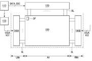
도 1 및 도 2에 도시된 바와 같이, 표시장치에는 표시패널(100), 타이밍 제어부(110), 데이터 구동부(120), 레벨 시프터 회로(130) 및 게이트 구동부(130, 140A, 140B)가 포함된다.1 and 2 , the display device includes a
표시패널(100)에는 상호 교차하는 데이터 라인들(DL) 및 게이트 라인들(GL)에 구분되어 연결된 서브 픽셀들이 포함된다. 표시패널(100)은 적어도 하나의 필름이나 기판 그리고 그 위에 형성된 서브 픽셀들을 수분이나 산소 등의 외기로부터 보호하기 위해 밀봉된다.The
표시패널(100)은 서브 픽셀들이 형성되는 표시영역(AA)과 표시영역(AA)의 외측으로 각종 신호라인들이나 패드 등이 형성되는 비표시영역(LNA, RNA)을 포함한다. 표시패널(100)은 서브 픽셀(SP)의 구성 방식에 따라 액정층이나 유기 발광층을 포함하는 형태로 구현된다.The
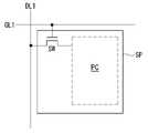
하나의 서브 픽셀(SP)에는 게이트 라인(GL1)과 데이터 라인(DL1)에 연결된 스위칭 트랜지스터(SW)와 스위칭 트랜지스터(SW)를 통해 공급된 게이트신호에 대응하여 공급된 데이터신호(DATA)에 대응하여 동작하는 픽셀회로(PC)가 포함된다. 서브 픽셀(SP)은 픽셀회로(PC)의 구성에 따라 액정층을 구동하거나 유기 발광층 등을 구동하기 위한 회로로 구현된다.In one sub-pixel SP, the switching transistor SW connected to the gate line GL1 and the data line DL1 corresponds to the data signal DATA supplied in response to the gate signal supplied through the switching transistor SW. and a pixel circuit (PC) that operates by The sub-pixel SP is implemented as a circuit for driving a liquid crystal layer or an organic light emitting layer according to the configuration of the pixel circuit PC.
타이밍 제어부(110)는 영상보드에 연결된 LVDS 또는 TMDS 인터페이스 수신회로 등을 통해 수직 동기신호, 수평 동기신호, 데이터 인에이블 신호, 도트 클럭 등의 타이밍신호를 입력받는다. 타이밍 제어부(110)는 입력된 타이밍신호를 기준으로 데이터 구동부(120)와 게이트 구동부(130, 140A, 140B)의 동작 타이밍을 제어하기 위한 타이밍 제어신호들을 발생한다.The
데이터 구동부(120)는 다수의 소스 드라이브 IC(Integrated Circuit)들을 포함한다. 소스 드라이브 IC들은 타이밍 제어부(110)로부터 데이터신호(DATA)와 소스 타이밍 제어신호(DDC)를 공급받는다. 소스 드라이브 IC들은 소스 타이밍 제어신호(DDC)에 응답하여 데이터신호(DATA)를 디지털신호에서 아날로그신호로 변환하고, 이를 표시패널(100)의 데이터 라인들(DL)을 통해 공급한다. 소스 드라이브 IC들은 COG(Chip On Glass) 공정이나 TAB(Tape Automated Bonding) 공정에 의해 표시패널(100)의 데이터 라인들(DL)에 접속된다.The
게이트 구동부(130, 140A, 140B)는 레벨 시프터 회로(130) 및 시프트 레지스터 회로(140A, 140B) 등을 포함한다. 시프트 레지스터 회로(140A, 140B)는 게이트인패널(Gate In Panel; 이하 GIP) 방식에 의해 표시패널(100)에 박막 트랜지스터 형태로 형성되거나 집적회로(IC) 형태로 형성되어 인쇄회로기판이나 연성회로기판 등에 실장된다. 이하, 게이트 구동부(140A, 140B)가 게이트인패널 방식으로 형성된 것을 일례로 설명한다.The
시프트 레지스터 회로(140A, 140B)는 표시패널(100)의 좌측 및 우측 비표시영역(LNA, RNA)에 구분되어 형성된다. 시프트 레지스터 회로(140A, 140B)는 레벨 시프터 회로(130)로부터 출력된 신호 등(GCLK, VST)을 기반으로 게이트신호를 시프트하고 출력하는 스테이지들로 이루어진다. 시프트 레지스터 회로(140A, 140B)는 서브 픽셀들에 포함된 스위칭 트랜지스터들을 턴온 또는 턴오프할 수 있는 전압 레벨로 게이트신호를 마련한다.The
도 1, 도 3 및 도 4에 도시된 바와 같이, 레벨 시프터 회로(130)는 전원 공급부(150)와 통합되거나 독립적인 IC로 구성될 수 있다. 이하에서는 설명의 편의를 위해 레벨 시프터 회로(130)가 독립적인 IC로 구성된 것을 일례로 설명한다.1 , 3 and 4 , the
레벨 시프터 회로(130)는 타이밍 제어부(110)의 제어하에 클록신호라인, 스타트신호라인 등을 통해 공급되는 게이트 클록신호 및 스타트신호(GCLK, VST) 등의 레벨을 시프팅한 후 시프트 레지스터 회로(140A, 140B)에 공급한다. 레벨 시프터 회로(130)는 전원 공급부(150)로부터 출력된 게이트하이전압(VGH)과 게이트로우전압(VGL)을 기반으로 게이트 클록신호(GCLK)를 생성 및 출력한다.The
레벨 시프터 회로(130)는 제어 회로부(136), 게이트 펄스 변조부(135) 및 클록신호 생성부(138)를 포함한다.The
제어 회로부(136)는 클록신호 생성부(138)를 제어한다. 제어 회로부(136)는 제어신호(TTC)를 기반으로 클록신호 생성부(138)를 제어한다. 클록신호 생성부(138)는 제어신호(TTC)에 대응하여 게이트하이전압(VGH)과 게이트로우전압(VGL)을 스위칭하며 게이트 클록신호들(GCLK1 ~ GCLKn)을 생성 및 출력한다.The
게이트 펄스 변조부(135)는 타이밍 제어부(110)로부터 출력된 온 클록신호(ONCLK) 및 오프 클록신호(OFFCLK)에 대응하여 클록신호 생성부(138)로부터 출력되는 게이트 클록신호들(GCLK1 ~ GCLKn)을 변조한다.The
온 클록신호(ONCLK) 및 오프 클록신호(OFFCLK)는 로직로우 구간이 지속되다가 로직하이 구간이 간헐적으로 나타나는 형태의 클록신호 형태로 형성된다. 온 클록신호(ONCLK)와 오프 클록신호(OFFCLK)는 로직하이 구간이 중첩하지 않도록 생성된다. 그러나 클록신호의 위상이 많아질 경우 온 클록신호(ONCLK) 및 오프 클록신호(OFFCLK)의 로직하이 구간 간의 간격은 점차 좁아질 수 있고 지연(RDLY) 저항 등에 의해 상호 중첩하는 구간이 발생할 수도 있다.The on-clock signal ONCLK and the off-clock signal OFFCLK are formed in the form of clock signals in which a logic low period is continued and a logic high period is intermittently displayed. The on-clock signal ONCLK and the off-clock signal OFFCLK are generated so that the logic high period does not overlap. However, when the phases of the clock signal increase, the interval between the logic-high sections of the on-clock signal ONCLK and the off-clock signal OFFCLK may gradually narrow, and a section overlapping each other may occur due to the delay RDLY resistance.
게이트 펄스 변조부(135)는 온 클록신호(ONCLK)에 대응하여 게이트 클록신호(GCLK)의 라이징 에지를 가변(GPMR)하고 오프 클록신호(OFFCLK)에 대응하여 게이트 클록신호(GCLK)의 폴링 에지를 가변(GPMF)한다.The
게이트 구동부(130, 140A, 140B)는 게이트 클록신호(GCLK)의 라이징 에지 및 게이트 클록신호(GCLK)의 폴링 에지 중 하나 이상을 가변하는 방식으로 소비전류를 개선 및 절감한다.The
그런데 게이트 구동부(130, 140A, 140B)는 게이트 클록신호의 위상이 늘어나면서 온 클록신호(ONCLK)와 오프 클록신호(OFFCLK) 간의 간격이 좁아지고 특정 구간에서 비정상적인 게이트 펄스의 변조가 일어나는 문제가 있어 이의 개선이 요구된다.However, in the
<실험예><Experimental example>
도 5는 실험예에 따른 레벨 시프터 회로의 클록신호 생성부를 개략적으로 나타낸 회로도이고, 도 6은 실험예의 문제점을 보여주는 파형도이다.5 is a circuit diagram schematically showing a clock signal generator of a level shifter circuit according to an experimental example, and FIG. 6 is a waveform diagram showing a problem of the experimental example.
도 3 및 도 5에 도시된 바와 같이, 실험예의 클록신호 생성부(138)에는 제1H트랜지스터(TH1), 제2H트랜지스터(TH2), 제1L트랜지스터(TL1) 및 제2L트랜지스터(TL2)가 포함된다. 그리고 게이트 펄스 변조부(135)에는 제1스위치(SW1) 및 제2스위치(SW2)가 포함된다.3 and 5, the
제1H트랜지스터(TH1) 및 제1L트랜지스터(TL1)는 제어 회로부(136)로부터 출력된 제어신호(TTC)에 응답하여 게이트하이전압(VGH)과 게이트로우전압(VGL)을 스위칭시키며 제A게이트 클록단자(GCLKA)를 통해 제A게이트 클록신호(GCLKA)를 출력한다.The first H transistor TH1 and the first L transistor TL1 switch the gate high voltage VGH and the gate low voltage VGL in response to the control signal TTC output from the
제2H트랜지스터(TH2) 및 제2L트랜지스터(TL2)는 제어 회로부(136)로부터 출력된 제어신호(TTC)에 응답하여 게이트하이전압(VGH)과 게이트로우전압(VGL)을 스위칭시키며 제B게이트 클록단자(GCLKB)를 통해 제B게이트 클록신호(GCLKB)를 출력한다.The second H transistor TH2 and the second L transistor TL2 switch the gate high voltage VGH and the gate low voltage VGL in response to the control signal TTC output from the
게이트 클록신호는 제A게이트 클록단자(GCLKA)를 통해 출력된 제A게이트 클록신호(GCLKA)와 제B게이트 클록단자(GCLKB)를 통해 출력된 제B게이트 클록신호(GCLKB)에 의해 로직하이와 로직로우 구간이 정의된다.The gate clock signal is at a logic high level by the A-th gate clock signal GCLKA output through the A-th gate clock terminal GCLKA and the B-th gate clock signal GCLKB output through the B-th gate clock terminal GCLKB. A logic low section is defined.
게이트 펄스 변조부(135)에는 제1스위치(SW1) 및 제2스위치(SW2)가 포함된다. 제1스위치(SW1)와 제2스위치(SW2)는 자신의 단자에 연결된 외부전압단자(RE)로 전류 패스를 형성(Path O)하거나 차단(Path X)한다. 이를 위해, 제1스위치(SW1)는 온 클록신호(ONCLK)의 하이에 대응하여 턴온 동작하고 온 클록신호(ONCLK)의 로우에 대응하여 턴오프 동작하고, 제2스위치(SW2)는 오프 클록신호(OFFCLK)의 하이에 대응하여 턴온 동작하고 온 클록신호(ONCLK)의 로우에 대응하여 턴오프 동작한다.The
외부전압단자(RE)에는 게이트하이전압(VGH)과 게이트로우전압(VGL)의 사이의 외부전압(AVDD)이 수동소자 예컨대 다이오드(D1)(회로의 구성에 따라 다이오드 대신 저항기로 대체될 수도 있음)를 거쳐 인가된다. 제1스위치(SW1) 및 제2스위치(SW2)가 턴온/턴오프될 때마다 외부전압단자(RE)에 인가된 외부전압(AVDD)에 대응하여 제A게이트 클록신호(GCLKA)와 제B게이트 클록단자(GCLKB)의 전류(전압)은 방전된다.At the external voltage terminal RE, an external voltage AVDD between the gate high voltage VGH and the gate low voltage VGL may be replaced with a passive element such as a diode D1 (a resistor instead of a diode depending on the circuit configuration) ) through which it is approved. Whenever the first switch SW1 and the second switch SW2 are turned on/off, the A-th gate clock signal GCLKA and the B-th gate correspond to the external voltage AVDD applied to the external voltage terminal RE. The current (voltage) of the clock terminal GCLKB is discharged.
게이트 펄스 변조부(135)는 온 클록신호(ONCLK)에 대응하여 게이트 클록신호(GCLK)의 라이징 에지를 가변(GPMR)(충전)하고 오프 클록신호(OFFCLK)에 대응하여 게이트 클록신호(GCLK)의 폴링 에지를 가변(GPMF)(방전)한다.The
실험예의 게이트 펄스 변조부(135)는 게이트 클록신호(GCLK)의 라이징 에지와 게이트 클록신호(GCLK)의 폴링 에지를 모두 가변한다. 그리고 실험예의 게이트 펄스 변조부(135)는 게이트 펄스 변조의 활성화 또는 비활성화 여부에 관계없이 온 클록신호(ONCLK) 및 오프 클록신호(OFFCLK)에 대응하여 제1스위치(SW1) 및 제2스위치(SW2)가 동작하도록 설정된다.The
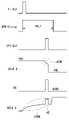
실험예는 4상이나 6상의 클록신호를 생성할 때에는 문제가 없었다. 하지만, 8상 이상의 클록신호를 형성할 경우, 온 클록신호(ONCLK) 및 오프 클록신호(OFFCLK) 간의 간격이 좁아짐에 따른 문제가 발생하였다.In the experimental example, there was no problem when generating a 4-phase or 6-phase clock signal. However, when an 8-phase or more clock signal is formed, a problem occurs due to a narrowing interval between the on-clock signal ONCLK and the off-clock signal OFFCLK.
일례로, 게이트 클록신호(GCLK)의 라이징 에지를 가변(GPMR)함과 더불어 게이트 클록신호(GCLK)의 폴링 에지를 가변(GPMF)하기 위한 옵션 사용시, 도 6과 같이 라이징 에지를 가변(GPMR)하는 구간과 폴링 에지를 가변(GPMF)하는 구간이 겹치게 되는 중첩 구간이 발생하였다.For example, when using an option for varying (GPMR) the rising edge of the gate clock signal GCLK and varying the falling edge of the gate clock signal GCLK (GPMF), as shown in FIG. 6 , the rising edge is variable (GPMR) There was an overlapping section in which the section for changing the falling edge (GPMF) overlapped.
그 결과, 실험예는 게이트 클록신호 간의 전류 패스(Current Path)가 비정상적으로 유기(GCLKA의 AB 참조)되면서 게이트 클록신호의 라이징 에지에 비정상적인 파형(GCLK Rising GPM Abnormal)을 형성하였다. 한편, 도 6에서 GPM Rising의 폭(width)은 On CLK Rising 시점부터 레벨 시프터의 내부에 마련된 RDLY 저항에 따른 폭(width)의 증가분에 의해 정의될 수 있다.
이상 실험예는 게이트 클록신호에 원치 않는 이상 파형이 발생할 경우 게이트 구동부의 구동 안정성이 저하됨은 물론 소비전류 절감 효과를 저하하고 더 나아가 표시패널의 화면 이상을 야기하는 것으로 나타났다.As a result, in the experimental example, an abnormal waveform (GCLK Rising GPM Abnormal) was formed at the rising edge of the gate clock signal as the current path between the gate clock signals was abnormally induced (see AB of GCLKA). Meanwhile, in FIG. 6 , the width of GPM Rising may be defined by an increase in width according to the RDLY resistance provided inside the level shifter from the time of On CLK Rising.
The above experimental example shows that when an unwanted abnormal waveform is generated in the gate clock signal, the driving stability of the gate driver is reduced, the effect of reducing current consumption is reduced, and furthermore, the screen of the display panel is abnormal.
삭제delete
<제1실시예><First embodiment>
도 7은 본 발명의 제1실시예에 따른 레벨 시프터 회로의 클록신호 생성부를 개략적으로 나타낸 회로도이고, 도 8은 제1실시예의 개선점을 보여주는 파형도이다.7 is a circuit diagram schematically showing a clock signal generator of the level shifter circuit according to the first embodiment of the present invention, and FIG. 8 is a waveform diagram showing improvements of the first embodiment.
도 3 및 도 7에 도시된 바와 같이, 제1실시예의 클록신호 생성부(138)에는 제1H트랜지스터(TH1), 제2H트랜지스터(TH2), 제1L트랜지스터(TL1) 및 제2L트랜지스터(TL2)가 포함된다. 그리고 제1실시예의 게이트 펄스 변조부(135)에는 제1스위치(SW1) 및 제2스위치(SW2)가 포함된다.3 and 7, in the
제1H트랜지스터(TH1) 및 제1L트랜지스터(TL1)는 제어 회로부(136)로부터 출력된 제어신호(TTC)에 응답하여 게이트하이전압(VGH)과 게이트로우전압(VGL)을 스위칭시키며 제A게이트 클록단자(GCLKA)를 통해 제A게이트 클록신호(GCLKA)를 출력한다.The first H transistor TH1 and the first L transistor TL1 switch the gate high voltage VGH and the gate low voltage VGL in response to the control signal TTC output from the
제1H트랜지스터(TH1)는 제어 회로부(136)의 제어신호라인에 게이트전극이 연결되고 게이트하이전압라인에 제1전극이 연결되고 제A게이트 클록단자(GCLKA)에 제2전극이 연결된다. 제1L트랜지스터(TL1)는 제어 회로부(136)의 제어신호라인에 게이트전극이 연결되고 게이트로우전압라인에 제1전극이 연결되고 제A게이트 클록단자(GCLKA)에 제2전극이 연결된다.The first H transistor TH1 has a gate electrode connected to the control signal line of the
제1H트랜지스터(TH1)가 턴온되면 제A게이트 클록단자(GCLKA)를 통해 게이트하이전압(VGH)(로직하이)에 대응하는 제A게이트 클록신호(GCLKA)가 출력된다. 제1L트랜지스터(TL1)가 턴온되면 제A게이트 클록단자(GCLKA)를 통해 게이트로우전압(VGL)(로직로우)에 대응하는 제A게이트 클록신호(GCLKA)가 출력된다.When the first H transistor TH1 is turned on, the A-th gate clock signal GCLKA corresponding to the gate high voltage VGH (logic high) is output through the A-th gate clock terminal GCLKA. When the first L transistor TL1 is turned on, the A-th gate clock signal GCLKA corresponding to the gate low voltage VGL (logic low) is output through the A-th gate clock terminal GCLKA.
제2H트랜지스터(TH2) 및 제2L트랜지스터(TL2)는 제어 회로부(136)로부터 출력된 제어신호(TTC)에 응답하여 게이트하이전압(VGH)과 게이트로우전압(VGL)을 스위칭시키며 제B게이트 클록단자(GCLKB)를 통해 제B게이트 클록신호(GCLKB)를 출력한다.The second H transistor TH2 and the second L transistor TL2 switch the gate high voltage VGH and the gate low voltage VGL in response to the control signal TTC output from the
제2H트랜지스터(TH2)는 제어 회로부(136)의 제어신호라인에 게이트전극이 연결되고 게이트하이전압라인에 제1전극이 연결되고 제B게이트 클록단자(GCLKB)에 제2전극이 연결된다. 제2L트랜지스터(TL2)는 제어 회로부(136)의 제어신호라인에 게이트전극이 연결되고 게이트로우전압라인에 제1전극이 연결되고 제B게이트 클록단자(GCLKB)에 제2전극이 연결된다.The second H transistor TH2 has a gate electrode connected to the control signal line of the
제2H트랜지스터(TH2)가 턴온되면 제B게이트 클록단자(GCLKB)를 통해 게이트하이전압(VGH)(로직하이)에 대응하는 제B게이트 클록신호(GCLKB)가 출력된다. 제2L트랜지스터(TL2)가 턴온되면 제B게이트 클록단자(GCLKB)를 통해 게이트로우전압(VGL)(로직로우)에 대응하는 제B게이트 클록신호(GCLKB)가 출력된다.When the second H transistor TH2 is turned on, the B-th gate clock signal GCLKB corresponding to the gate high voltage VGH (logic high) is output through the B-th gate clock terminal GCLKB. When the second L transistor TL2 is turned on, the B-th gate clock signal GCLKB corresponding to the gate low voltage VGL (logic low) is output through the B-th gate clock terminal GCLKB.
게이트 클록신호는 제A게이트 클록단자(GCLKA)를 통해 출력된 제A게이트 클록신호(GCLKA)와 제B게이트 클록단자(GCLKB)를 통해 출력된 제B게이트 클록신호(GCLKB)에 의해 로직하이와 로직로우 구간이 정의된다.The gate clock signal is at a logic high level by the A-th gate clock signal GCLKA output through the A-th gate clock terminal GCLKA and the B-th gate clock signal GCLKB output through the B-th gate clock terminal GCLKB. A logic low section is defined.
게이트 펄스 변조부(135)에는 제1스위치(SW1) 및 제2스위치(SW2)가 포함된다. 제1스위치(SW1)는 제A게이트 클록단자(GCLKA)에 제1전극이 연결되고 외부전압단자(RE)에 제2전극이 연결된다. 제2스위치(SW2)는 제B게이트 클록단자(GCLKB)에 제1전극이 연결되고 외부전압단자(RE)에 제2전극이 연결된다.The
제1스위치(SW1)와 제2스위치(SW2)는 자신의 단자에 연결된 외부전압단자(RE)로 전류 패스를 형성(Path O)하거나 차단(Path X)한다. 이를 위해, 제1스위치(SW1)는 온 클록신호(ONCLK)의 하이에 대응하여 턴온 동작하고 온 클록신호(ONCLK)의 로우에 대응하여 턴오프 동작하고, 제2스위치(SW2)는 오프 클록신호(OFFCLK)의 하이에 대응하여 턴온 동작하고 온 클록신호(ONCLK)의 로우에 대응하여 턴오프 동작한다.The first switch SW1 and the second switch SW2 form (Path O) or block (Path X) a current path to the external voltage terminal RE connected to their terminals. To this end, the first switch SW1 turns on in response to the high level of the on clock signal ONCLK and turns off in response to the low level of the on clock signal ONCLK, and the second switch SW2 operates on the off clock signal The turn-on operation is performed in response to the high level of (OFFCLK) and the turn-off operation is performed in response to the low level of the on-clock signal ONCLK.
외부전압단자(RE)에는 게이트하이전압(VGH)과 게이트로우전압(VGL)의 사이의 외부전압(AVDD)이 수동소자 예컨대 다이오드(D1)(회로의 구성에 따라 다이오드 대신 저항기로 대체되거나 수동소자가 제거될 수도 있음)를 거쳐 인가된다. 제1스위치(SW1) 및 제2스위치(SW2)가 턴온/턴오프될 때마다 외부전압단자(RE)에 인가된 외부전압(AVDD)에 대응하여 제A게이트 클록신호(GCLKA)와 제B게이트 클록단자(GCLKB)의 전류(전압)은 방전된다.At the external voltage terminal RE, an external voltage AVDD between the gate high voltage VGH and the gate low voltage VGL is applied to a passive device such as a diode D1 (depending on the circuit configuration, a resistor may be replaced with a resistor or a passive device). may be removed). Whenever the first switch SW1 and the second switch SW2 are turned on/off, the A-th gate clock signal GCLKA and the B-th gate correspond to the external voltage AVDD applied to the external voltage terminal RE. The current (voltage) of the clock terminal GCLKB is discharged.
게이트 펄스 변조부(135)는 온 클록신호(ONCLK)에 대응하여 게이트 클록신호(GCLK)의 라이징 에지를 가변(GPMR)(충전)하고 오프 클록신호(OFFCLK)에 대응하여 게이트 클록신호(GCLK)의 폴링 에지를 가변(GPMF)(방전)한다.The
제1실시예의 게이트 펄스 변조부(135)는 게이트 클록신호(GCLK)의 라이징 에지 또는 게이트 클록신호(GCLK)의 폴링 에지 중 하나만 가변한다.The
제1실시예와 같이, 게이트 클록신호(GCLK)의 라이징 에지 또는 게이트 클록신호(GCLK)의 폴링 에지 중 하나만 가변할 경우 게이트 펄스 변조부(135)는 제1스위치(SW1) 및 제2스위치(SW2) 중 하나를 턴오프 시킨다.As in the first embodiment, when only one of the rising edge of the gate clock signal GCLK or the falling edge of the gate clock signal GCLK is varied, the
도 7 및 도 8은 제2스위치(SW2)만 턴오프되어 게이트 클록신호(GCLK)의 라이징 에지만 가변(GPMR)하는 회로 및 파형을 일례로 도시한 것이다.7 and 8 illustrate, as an example, a circuit and a waveform in which only the second switch SW2 is turned off to vary (GPMR) only the rising edge of the gate clock signal GCLK.
일례로, 게이트 클록신호의 라이징 에지 가변만 사용할 경우, 오프 클록신호(OFFCLK)의 폭은 의미가 없다(Off CLK Width는 Falling GPM의 Width를 결정하기 위해 사용됨). 그러므로, 오프 클록신호(OFFCLK)가 입력될 경우, 제2스위치(SW2)를 턴오프시켜 게이트 클록신호 간의 전류 패스(Current Path)가 발생하는 문제는 제거된다.For example, when only the variable rising edge of the gate clock signal is used, the width of the off clock signal OFFCLK is meaningless (Off CLK Width is used to determine the width of the falling GPM). Therefore, when the off clock signal OFFCLK is input, the problem that a current path occurs between the gate clock signals by turning off the second switch SW2 is eliminated.
다른 예로, 게이트 클록신호의 폴링 에지 가변만 사용할 경우, 온 클록신호(ONCLK)의 폭은 의미가 없다(On CLK Width는 Rising GPM의 Width를 결정하기 위해 사용됨). 그러므로, 온 클록신호(ONCLK)가 입력될 경우, 제1스위치(SW1)를 턴오프시켜 게이트 클록신호 간의 전류 패스(Current Path)가 발생하는 문제는 제거된다.As another example, when only the variable falling edge of the gate clock signal is used, the width of the on clock signal ONCLK is meaningless (On CLK Width is used to determine the width of the rising GPM). Therefore, when the on clock signal ONCLK is input, the problem that a current path occurs between the gate clock signals by turning off the first switch SW1 is eliminated.
이를 위해, 게이트 펄스 변조부(135)는 오프 클록신호(OFFCLK)와 온 클록신호(ONCLK)의 펄스폭을 센싱하고 이 신호들이 내부에 설정된 특정 범위 예컨대, 150ns ~ 200ns 펄스폭을 갖는지를 판단하는 센싱회로를 갖는다.To this end, the
센싱회로는 오프 클록신호(OFFCLK)와 온 클록신호(ONCLK)의 펄스폭이 위의 범위에 들어오면, 게이트 클록신호(GCLK)의 라이징 에지 또는 게이트 클록신호(GCLK)의 폴링 에지 중 하나만 가변하는 것으로 판단하고 제1스위치(SW1) 및 제2스위치(SW2) 중 하나를 턴오프 시킨다.When the pulse widths of the off-clock signal OFFCLK and the on-clock signal ONCLK fall within the above range, the sensing circuit changes only one of the rising edge of the gate clock signal GCLK or the falling edge of the gate clock signal GCLK. and turns off one of the first switch SW1 and the second switch SW2.
4상이나 6상의 게이트 클록신호를 생성할 때에는 게이트 클록신호(GCLK)의 라이징 에지 및 게이트 클록신호(GCLK)의 폴링 에지를 모두 사용한다. 그러나, 레벨 시프터 회로가 8상 이상의 게이트 클록신호를 형성할 경우, 온 클록신호(ONCLK) 및 오프 클록신호(OFFCLK) 간의 간격이 좁아짐에 따른 문제를 해소하기 위해 게이트 클록신호(GCLK)의 라이징 에지 및 게이트 클록신호(GCLK)의 폴링 에지 중 하나만 사용한다.When generating the 4-phase or 6-phase gate clock signal, both the rising edge of the gate clock signal GCLK and the falling edge of the gate clock signal GCLK are used. However, when the level shifter circuit forms a gate clock signal of 8 or more phases, the rising edge of the gate clock signal GCLK may and only one of the falling edges of the gate clock signal GCLK is used.
그 결과, 제1실시예는 게이트 클록신호의 라이징 에지 또는 게이트 클록신호의 라이징 폴링에 비정상적인 파형(GCLK GPM Abnormal)이 형성되는 문제가 해소되는 것으로 나타났다.As a result, it was found that the first embodiment solves the problem that an abnormal waveform (GCLK GPM Abnormal) is formed at the rising edge of the gate clock signal or the rising falling of the gate clock signal.
<제2실시예><Second embodiment>
도 9는 본 발명의 제2실시예에 따른 레벨 시프터 회로의 개략적인 구성 예시도이고, 도 10은 본 발명의 제2실시예에 따른 레벨 시프터 회로의 클록신호 생성부를 개략적으로 나타낸 회로도이고, 도 11은 제2실시예의 개선점을 보여주는 파형도이다.9 is a schematic configuration diagram of a level shifter circuit according to a second embodiment of the present invention, and FIG. 10 is a circuit diagram schematically showing a clock signal generator of a level shifter circuit according to a second embodiment of the present invention, FIG. 11 is a waveform diagram showing the improvement of the second embodiment.
도 9에 도시된 바와 같이, 레벨 시프터 회로(130)는 제어 회로부(136), 게이트 펄스 변조부(135) 및 클록신호 생성부(138)를 포함한다.As shown in FIG. 9 , the
제어 회로부(136)는 클록신호 생성부(138)를 제어한다. 제어 회로부(136)는 제어신호(TTC)를 기반으로 클록신호 생성부(138)를 제어한다. 클록신호 생성부(138)는 제어신호(TTC)에 대응하여 게이트하이전압(VGH)과 게이트로우전압(VGL)을 스위칭하며 게이트 클록신호들(GCLK1 ~ GCLKn)을 생성 및 출력한다.The
게이트 펄스 변조부(135)는 게이트 펄스 제어신호(GPMCS), 온 클록신호(ONCLK) 및 오프 클록신호(OFFCLK)에 대응하여 클록신호 생성부(138)로부터 출력되는 게이트 클록신호들(GCLK1 ~ GCLKn)을 변조한다.The
게이트 펄스 제어신호(GPMCS)는 레벨 시프터 회로(130)의 내부 또는 타이밍 제어부(110)로부터 생성될 수 있다. 이하에서는 게이트 펄스 제어신호(GPMCS)가 타이밍 제어부(110)로부터 출력되는 것을 일례로 설명한다.The gate pulse control signal GPMCS may be generated inside the
게이트 펄스 변조부(135)는 타이밍 제어부(110)로부터 출력된 게이트 펄스 제어신호(GPMCS)와 온 클록신호(ONCLK)에 대응하여 게이트 클록신호(GCLK)의 라이징 에지를 가변(GPMR)하거나 게이트 펄스 제어신호(GPMCS)와 오프 클록신호(OFFCLK)에 대응하여 게이트 클록신호(GCLK)의 폴링 에지를 가변(GPMF)한다.The
도 9 및 도 10에 도시된 바와 같이, 제2실시예의 클록신호 생성부(138)에는 제1H트랜지스터(TH1), 제2H트랜지스터(TH2), 제1L트랜지스터(TL1), 제2L트랜지스터(TL2), 제1스위치(SW1) 및 제2스위치(SW2)가 포함된다.9 and 10 , the
제1H트랜지스터(TH1) 및 제1L트랜지스터(TL1)는 제어 회로부(136)로부터 출력된 제어신호(TTC)에 응답하여 게이트하이전압(VGH)과 게이트로우전압(VGL)을 스위칭시키며 제A게이트 클록단자(GCLKA)를 통해 제A게이트 클록신호(GCLKA)를 출력한다.The first H transistor TH1 and the first L transistor TL1 switch the gate high voltage VGH and the gate low voltage VGL in response to the control signal TTC output from the
제1H트랜지스터(TH1)는 제어 회로부(136)의 제어신호라인에 게이트전극이 연결되고 게이트하이전압라인에 제1전극이 연결되고 제A게이트 클록단자(GCLKA)에 제2전극이 연결된다. 제1L트랜지스터(TL1)는 제어 회로부(136)의 제어신호라인에 게이트전극이 연결되고 게이트로우전압라인에 제1전극이 연결되고 제A게이트 클록단자(GCLKA)에 제2전극이 연결된다.The first H transistor TH1 has a gate electrode connected to the control signal line of the
제1H트랜지스터(TH1)가 턴온되면 제A게이트 클록단자(GCLKA)를 통해 게이트하이전압(VGH)(로직하이)에 대응하는 제A게이트 클록신호(GCLKA)가 출력된다. 제1L트랜지스터(TL1)가 턴온되면 제A게이트 클록단자(GCLKA)를 통해 게이트로우전압(VGL)(로직로우)에 대응하는 제A게이트 클록신호(GCLKA)가 출력된다.When the first H transistor TH1 is turned on, the A-th gate clock signal GCLKA corresponding to the gate high voltage VGH (logic high) is output through the A-th gate clock terminal GCLKA. When the first L transistor TL1 is turned on, the A-th gate clock signal GCLKA corresponding to the gate low voltage VGL (logic low) is output through the A-th gate clock terminal GCLKA.
제2H트랜지스터(TH2) 및 제2L트랜지스터(TL2)는 제어 회로부(136)로부터 출력된 제어신호(TTC)에 응답하여 게이트하이전압(VGH)과 게이트로우전압(VGL)을 스위칭시키며 제B게이트 클록단자(GCLKB)를 통해 제B게이트 클록신호(GCLKB)를 출력한다.The second H transistor TH2 and the second L transistor TL2 switch the gate high voltage VGH and the gate low voltage VGL in response to the control signal TTC output from the
제2H트랜지스터(TH2)는 제어 회로부(136)의 제어신호라인에 게이트전극이 연결되고 게이트하이전압라인에 제1전극이 연결되고 제B게이트 클록단자(GCLKB)에 제2전극이 연결된다. 제2L트랜지스터(TL2)는 제어 회로부(136)의 제어신호라인에 게이트전극이 연결되고 게이트로우전압라인에 제1전극이 연결되고 제B게이트 클록단자(GCLKB)에 제2전극이 연결된다.The second H transistor TH2 has a gate electrode connected to the control signal line of the
제2H트랜지스터(TH2)가 턴온되면 제B게이트 클록단자(GCLKB)를 통해 게이트하이전압(VGH)(로직하이)에 대응하는 제B게이트 클록신호(GCLKB)가 출력된다. 제2L트랜지스터(TL2)가 턴온되면 제B게이트 클록단자(GCLKB)를 통해 게이트로우전압(VGL)(로직로우)에 대응하는 제B게이트 클록신호(GCLKB)가 출력된다.When the second H transistor TH2 is turned on, the B-th gate clock signal GCLKB corresponding to the gate high voltage VGH (logic high) is output through the B-th gate clock terminal GCLKB. When the second L transistor TL2 is turned on, the B-th gate clock signal GCLKB corresponding to the gate low voltage VGL (logic low) is output through the B-th gate clock terminal GCLKB.
게이트 클록신호는 제A게이트 클록단자(GCLKA)를 통해 출력된 제A게이트 클록신호(GCLKA)와 제B게이트 클록단자(GCLKB)를 통해 출력된 제B게이트 클록신호(GCLKB)에 의해 로직하이와 로직로우 구간이 정의된다.The gate clock signal is at a logic high level by the A-th gate clock signal GCLKA output through the A-th gate clock terminal GCLKA and the B-th gate clock signal GCLKB output through the B-th gate clock terminal GCLKB. A logic low section is defined.
게이트 펄스 변조부(135)에는 제1스위치(SW1) 및 제2스위치(SW2)가 포함된다. 제1스위치(SW1)는 제A게이트 클록단자(GCLKA)에 제1전극이 연결되고 외부전압단자(RE)에 제2전극이 연결된다. 제2스위치(SW2)는 제B게이트 클록단자(GCLKB)에 제1전극이 연결되고 외부전압단자(RE)에 제2전극이 연결된다.The
제1스위치(SW1) 및 제2스위치(SW2)는 온 클록신호(ONCLK) 및 오프 클록신호(OFFCLK)에 대응하여 턴온/턴오프 동작하며, 자신의 단자에 연결된 외부전압단자(RE)로 전류 패스를 형성(Path O)하거나 차단(Path X)한다.The first switch SW1 and the second switch SW2 are turned on/off in response to the on-clock signal ONCLK and the off-clock signal OFFCLK, and current flows to the external voltage terminal RE connected to their terminals. It forms a path (Path O) or blocks it (Path X).
외부전압단자(RE)에는 게이트하이전압(VGH)과 게이트로우전압(VGL)의 사이의 외부전압(AVDD)이 수동소자 예컨대 다이오드(D1)(회로의 구성에 따라 다이오드 대신 저항기로 대체되거나 수동소자가 제거될 수도 있음)를 거쳐 인가된다. 제1스위치(SW1) 및 제2스위치(SW2)가 턴온/턴오프될 때마다 외부전압단자(RE)에 인가된 외부전압(AVDD)에 대응하여 제A게이트 클록신호(GCLKA)와 제B게이트 클록단자(GCLKB)의 전류(전압)은 방전된다.At the external voltage terminal RE, an external voltage AVDD between the gate high voltage VGH and the gate low voltage VGL is applied to a passive device such as a diode D1 (depending on the circuit configuration, a resistor may be replaced with a resistor or a passive device). may be removed). Whenever the first switch SW1 and the second switch SW2 are turned on/off, the A-th gate clock signal GCLKA and the B-th gate correspond to the external voltage AVDD applied to the external voltage terminal RE. The current (voltage) of the clock terminal GCLKB is discharged.
게이트 펄스 변조부(135)는 타이밍 제어부(110)로부터 출력된 게이트 펄스 제어신호(GPMCS), 온 클록신호(ONCLK) 및 오프 클록신호(OFFCLK)에 대응하여 클록신호 생성부(138)로부터 출력되는 게이트 클록신호들(GCLK1 ~ GCLKn)을 변조한다.The
게이트 펄스 변조부(135)는 타이밍 제어부(110)로부터 출력된 게이트 펄스 제어신호(GPMCS)와 온 클록신호(ONCLK)에 대응하여 게이트 클록신호(GCLK)의 라이징 에지를 가변(GPMR)(충전)하거나 게이트 펄스 제어신호(GPMCS)와 오프 클록신호(OFFCLK)에 대응하여 게이트 클록신호(GCLK)의 폴링 에지를 가변(GPMF)(방전)한다.The
제2실시예의 게이트 펄스 변조부(135)는 게이트 클록신호(GCLK)의 라이징 에지 또는 게이트 클록신호(GCLK)의 폴링 에지 중 하나만 가변한다. 제2실시예와 같이, 게이트 클록신호(GCLK)의 라이징 에지 또는 게이트 클록신호(GCLK)의 폴링 에지 중 하나만 가변할 경우 게이트 펄스 변조부(135)는 제1스위치(SW1) 및 제2스위치(SW2) 중 하나를 강제적으로 턴오프 시킨다. 도 10 및 도 11은 제2스위치(SW2)만 턴오프되어 게이트 클록신호(GCLK)의 라이징 에지만 가변(GPMR)하는 회로 및 파형을 일례로 도시한 것이다.The
일례로, 게이트 클록신호의 라이징 에지 가변만 사용할 경우, 오프 클록신호(OFFCLK)가 입력되더라도 게이트 펄스 제어신호(GPMCS)에 의해 제2스위치(SW2)는 턴오프되므로 게이트 클록신호 간의 전류 패스(Current Path)가 발생하는 문제는 제거된다.For example, when only the variable rising edge of the gate clock signal is used, the second switch SW2 is turned off by the gate pulse control signal GPMCS even when the off clock signal OFFCLK is input. Path) is eliminated.
다른 예로, 게이트 클록신호의 폴링 에지 가변만 사용할 경우, 온 클록신호(ONCLK)가 입력되더라도 게이트 펄스 제어신호(GPMCS)에 의해 제1스위치(SW1)는 턴오프되므로 게이트 클록신호 간의 전류 패스(Current Path)가 발생하는 문제는 제거된다.As another example, when only the variable falling edge of the gate clock signal is used, the first switch SW1 is turned off by the gate pulse control signal GPMCS even when the on clock signal ONCLK is input. Path) is eliminated.
4상이나 6상의 게이트 클록신호를 생성할 때에는 게이트 클록신호(GCLK)의 라이징 에지 및 게이트 클록신호(GCLK)의 폴링 에지를 모두 사용한다. 그러나, 레벨 시프터 회로가 8상 이상의 게이트 클록신호를 형성할 경우, 온 클록신호(ONCLK) 및 오프 클록신호(OFFCLK) 간의 간격이 좁아짐에 따른 문제를 해소하기 위해 게이트 클록신호(GCLK)의 라이징 에지 및 게이트 클록신호(GCLK)의 폴링 에지 중 하나만 사용한다.When generating the 4-phase or 6-phase gate clock signal, both the rising edge of the gate clock signal GCLK and the falling edge of the gate clock signal GCLK are used. However, when the level shifter circuit forms a gate clock signal of 8 or more phases, the rising edge of the gate clock signal GCLK may and only one of the falling edges of the gate clock signal GCLK is used.
그 결과, 제2실시예는 게이트 클록신호의 라이징 에지 또는 게이트 클록신호의 라이징 폴링에 비정상적인 파형(GCLK GPM Abnormal)이 형성되는 문제가 해소되는 것으로 나타났다.As a result, it was found that the second embodiment solves the problem that an abnormal waveform (GCLK GPM Abnormal) is formed at the rising edge of the gate clock signal or the rising falling of the gate clock signal.
이상 본 발명은 게이트 클록신호에 원치 않는 이상 파형이 발생하는 문제를 해소하여 게이트 구동부의 구동 안정성을 향상하고 소비전류 절감 효과를 향상하고 더 나아가 표시패널의 화면 품위를 향상할 수 있는 효과가 있다.As described above, the present invention has the effect of improving the driving stability of the gate driver by solving the problem of generating an unwanted abnormal waveform in the gate clock signal, improving the effect of reducing current consumption, and further improving the screen quality of the display panel.
이상 첨부된 도면을 참조하여 본 발명의 실시예를 설명하였지만, 상술한 본 발명의 기술적 구성은 본 발명이 속하는 기술 분야의 당업자가 본 발명의 그 기술적 사상이나 필수적 특징을 변경하지 않고서 다른 구체적인 형태로 실시될 수 있다는 것을 이해할 수 있을 것이다. 그러므로 이상에서 기술한 실시 예들은 모든 면에서 예시적인 것이며 한정적인 것이 아닌 것으로서 이해되어야 한다. 아울러, 본 발명의 범위는 상기 상세한 설명보다는 후술하는 특허청구범위에 의하여 나타내어진다. 또한, 특허청구범위의 의미 및 범위 그리고 그 등가 개념으로부터 도출되는 모든 변경 또는 변형된 형태가 본 발명의 범위에 포함되는 것으로 해석되어야 한다.Although the embodiments of the present invention have been described above with reference to the accompanying drawings, the technical configuration of the present invention can be changed to other specific forms by those skilled in the art to which the present invention pertains without changing the technical spirit or essential features of the present invention. It will be appreciated that this may be practiced. Therefore, it should be understood that the embodiments described above are illustrative in all respects and not restrictive. In addition, the scope of the present invention is indicated by the claims to be described later rather than the above detailed description. In addition, all changes or modifications derived from the meaning and scope of the claims and their equivalents should be construed as being included in the scope of the present invention.
100: 표시패널110: 타이밍 제어부
120: 데이터 구동부130, 140A, 140B: 게이트 구동부
130: 레벨 시프터 회로140A, 140B: 시프트 레지스터 회로
136: 제어 회로부135:게이트 펄스 변조부
138: 클록신호 생성부ONCLK: 온 클록신호
OFFCLK: 오프 클록신호GCLK: 게이트 클록신호100: display panel 110: timing control unit
120:
130:
136: control circuit unit 135: gate pulse modulation unit
138: clock signal generator ONCLK: on clock signal
OFFCLK: Off clock signal GCLK: Gate clock signal
Claims (11)
Translated fromKorean상기 레벨 시프터 회로로부터 출력된 신호를 기반으로 게이트신호를 시프트하여 출력하는 스테이지들로 이루어진 시프트 레지스터 회로를 포함하고,
상기 레벨 시프터 회로는 게이트하이전압과 게이트로우전압을 스위칭하며 게이트 클록신호들을 생성하는 클록신호 생성부와,
외부로부터 공급된 온 클록신호 및 오프 클록신호에 대응하여 상기 클록신호 생성부로부터 출력되는 상기 게이트 클록신호들의 라이징 에지와 폴링 에지 중 하나를 선택적으로 변조하는 게이트 펄스 변조부를 포함하고,
상기 게이트 펄스 변조부는
상기 게이트 클록신호들을 출력하는 단자를 외부전압단자에 연결하여 전류 패스를 형성하는 제1스위치 및 제2스위치를 포함하고,
상기 제1스위치는 상기 온 클록신호의 하이에 대응하여 턴온 동작하고 상기 온 클록신호의 로우에 대응하여 턴오프 동작하고,
상기 제2스위치는 상기 오프 클록신호의 하이에 대응하여 턴온 동작하고 상기 오프 클록신호의 로우에 대응하여 턴오프 동작하고,
상기 게이트 펄스 변조부는
상기 온 클록신호의 펄스폭과 상기 오프 클록신호의 펄스폭을 센싱하고 내부에 설정된 펄스폭의 범위 내에 존재하면 상기 게이트 클록신호들의 라이징 에지와 폴링 에지 중 하나만 가변하기 위해 상기 제1스위치와 상기 제2스위치 중 하나를 강제로 턴오프하는 게이트 구동부.a level shifter circuit for outputting a signal; and
a shift register circuit including stages for shifting and outputting a gate signal based on a signal output from the level shifter circuit;
The level shifter circuit includes a clock signal generator that switches a gate high voltage and a gate low voltage and generates gate clock signals;
a gate pulse modulator for selectively modulating one of a rising edge and a falling edge of the gate clock signals output from the clock signal generator in response to an on clock signal and an off clock signal supplied from the outside;
The gate pulse modulator
a first switch and a second switch for forming a current path by connecting a terminal for outputting the gate clock signals to an external voltage terminal;
the first switch is turned on in response to the high of the on-clock signal and turns off in response to the low of the on-clock signal;
the second switch turns on in response to the high of the off-clock signal and turns off in response to the low of the off-clock signal;
The gate pulse modulator
When the pulse width of the on-clock signal and the pulse width of the off-clock signal are sensed, and only one of the rising edge and the falling edge of the gate clock signals is changed when it is within the range of the pulse width set therein, the first switch and the second switch A gate driver that forcibly turns off one of the two switches.
상기 표시패널에 데이터신호를 공급하는 데이터 구동부; 및
상기 표시패널에 게이트신호를 공급하는 게이트 구동부를 포함하고,
상기 게이트 구동부는 신호를 출력하는 레벨 시프터 회로와 상기 레벨 시프터 회로로부터 출력된 신호를 기반으로 상기 게이트신호를 시프트하여 출력하는 스테이지들로 이루어진 시프트 레지스터 회로를 포함하고,
상기 레벨 시프터 회로는 게이트하이전압과 게이트로우전압을 스위칭하며 게이트 클록신호들을 생성하는 클록신호 생성부와,
외부로부터 공급된 온 클록신호 및 오프 클록신호에 대응하여 상기 클록신호 생성부로부터 출력되는 상기 게이트 클록신호들의 라이징 에지와 폴링 에지 중 하나를 선택적으로 변조하는 게이트 펄스 변조부를 포함하고,
상기 게이트 펄스 변조부는
상기 게이트 클록신호들을 출력하는 단자를 외부전압단자에 연결하여 전류 패스를 형성하는 제1스위치 및 제2스위치를 포함하고,
상기 제1스위치는 상기 온 클록신호의 하이에 대응하여 턴온 동작하고 상기 온 클록신호의 로우에 대응하여 턴오프 동작하고,
상기 제2스위치는 상기 오프 클록신호의 하이에 대응하여 턴온 동작하고 상기 오프 클록신호의 로우에 대응하여 턴오프 동작하고,
상기 게이트 펄스 변조부는
상기 온 클록신호의 펄스폭과 상기 오프 클록신호의 펄스폭을 센싱하고 내부에 설정된 펄스폭의 범위 내에 존재하면 상기 게이트 클록신호들의 라이징 에지와 폴링 에지 중 하나만 가변하기 위해 상기 제1스위치와 상기 제2스위치 중 하나를 강제로 턴오프하는 표시장치.a display panel for displaying an image;
a data driver supplying a data signal to the display panel; and
a gate driver supplying a gate signal to the display panel;
The gate driver includes a shift register circuit including a level shifter circuit for outputting a signal and stages for shifting and outputting the gate signal based on a signal output from the level shifter circuit,
The level shifter circuit includes a clock signal generator that switches a gate high voltage and a gate low voltage and generates gate clock signals;
a gate pulse modulator for selectively modulating one of a rising edge and a falling edge of the gate clock signals output from the clock signal generator in response to an on clock signal and an off clock signal supplied from the outside;
The gate pulse modulator
a first switch and a second switch for forming a current path by connecting a terminal for outputting the gate clock signals to an external voltage terminal;
the first switch is turned on in response to the high of the on-clock signal and turns off in response to the low of the on-clock signal;
the second switch turns on in response to the high of the off-clock signal and turns off in response to the low of the off-clock signal;
The gate pulse modulator
When the pulse width of the on-clock signal and the pulse width of the off-clock signal are sensed, and only one of the rising edge and the falling edge of the gate clock signals is changed when it is within the range of the pulse width set therein, the first switch and the second switch 2 An indicator that forcibly turns off one of the switches.
상기 내부에 설정된 펄스폭의 범위는
150ns ~ 200ns인 표시장치.8. The method of claim 7,
The range of the pulse width set inside the
Display from 150ns to 200ns.
Priority Applications (1)
| Application Number | Priority Date | Filing Date | Title |
|---|---|---|---|
| KR1020150191823AKR102461388B1 (en) | 2015-12-31 | 2015-12-31 | Scan Driver and Display Device Using the same |
Applications Claiming Priority (1)
| Application Number | Priority Date | Filing Date | Title |
|---|---|---|---|
| KR1020150191823AKR102461388B1 (en) | 2015-12-31 | 2015-12-31 | Scan Driver and Display Device Using the same |
Publications (2)
| Publication Number | Publication Date |
|---|---|
| KR20170081088A KR20170081088A (en) | 2017-07-11 |
| KR102461388B1true KR102461388B1 (en) | 2022-11-01 |
Family
ID=59354778
Family Applications (1)
| Application Number | Title | Priority Date | Filing Date |
|---|---|---|---|
| KR1020150191823AActiveKR102461388B1 (en) | 2015-12-31 | 2015-12-31 | Scan Driver and Display Device Using the same |
Country Status (1)
| Country | Link |
|---|---|
| KR (1) | KR102461388B1 (en) |
Families Citing this family (3)
| Publication number | Priority date | Publication date | Assignee | Title |
|---|---|---|---|---|
| KR102460501B1 (en) | 2018-02-20 | 2022-10-31 | 삼성디스플레이 주식회사 | Display device and method of driving the same |
| KR102611008B1 (en) | 2019-06-13 | 2023-12-07 | 엘지디스플레이 주식회사 | Display device and driving method thereof |
| CN117672109B (en)* | 2023-12-13 | 2024-12-06 | 长沙惠科光电有限公司 | Display panel driving circuit, display panel and display device |
Citations (1)
| Publication number | Priority date | Publication date | Assignee | Title |
|---|---|---|---|---|
| US20100134172A1 (en)* | 2008-11-28 | 2010-06-03 | Chao-Ching Hsu | Charge-sharing method and device for clock signal generation |
Family Cites Families (3)
| Publication number | Priority date | Publication date | Assignee | Title |
|---|---|---|---|---|
| KR101385473B1 (en)* | 2007-08-20 | 2014-04-17 | 엘지디스플레이 주식회사 | A clock generator |
| KR101310378B1 (en)* | 2008-11-19 | 2013-09-23 | 엘지디스플레이 주식회사 | Liquid crystal display |
| KR101992160B1 (en)* | 2012-10-30 | 2019-06-24 | 엘지디스플레이 주식회사 | Display Device and Driving Method the same |
- 2015
- 2015-12-31KRKR1020150191823Apatent/KR102461388B1/enactiveActive
Patent Citations (1)
| Publication number | Priority date | Publication date | Assignee | Title |
|---|---|---|---|---|
| US20100134172A1 (en)* | 2008-11-28 | 2010-06-03 | Chao-Ching Hsu | Charge-sharing method and device for clock signal generation |
Also Published As
| Publication number | Publication date |
|---|---|
| KR20170081088A (en) | 2017-07-11 |
Similar Documents
| Publication | Publication Date | Title |
|---|---|---|
| KR102169169B1 (en) | Display device and method for driving the same | |
| KR102114155B1 (en) | Display device and driving method thereof | |
| US20080192032A1 (en) | Display apparatus and method of driving the same | |
| KR101661026B1 (en) | Display device | |
| KR20160077315A (en) | Scan driver and display device using thereof | |
| KR102379188B1 (en) | Display device and driving method of the same | |
| KR20220093764A (en) | Gate Driving Circuit and Organic Light Emitting Display using the same | |
| KR102573311B1 (en) | Display Device Of Active Matrix Type | |
| KR102461388B1 (en) | Scan Driver and Display Device Using the same | |
| KR20180059635A (en) | Gate driving circuit and display device using the same | |
| KR101969411B1 (en) | Liquid crystal display device and clock pulse generation circuit thereof | |
| KR101325199B1 (en) | Display device and method for driving the same | |
| KR102364096B1 (en) | Display Device | |
| KR20230101617A (en) | Gate Driving Circuit and Display Device using the same | |
| US20170148407A1 (en) | Display Device and Driving Method Thereof | |
| KR102461390B1 (en) | Gate Pulse Modulation Circuit and Display Device Using the same | |
| KR101989931B1 (en) | Liquid crystal display and undershoot generation circuit thereof | |
| CN107799046B (en) | Display device and controller | |
| KR20070041829A (en) | Flat Panel Display and Driving Method | |
| KR102495831B1 (en) | Scan Driver, Display Device and Driving Method of Display Device | |
| KR102049733B1 (en) | Liquid crystal display and method of driving the same | |
| KR20230102585A (en) | Gate Driving Circuit and Display Device using the same | |
| KR102283377B1 (en) | Display device and gate driving circuit thereof | |
| KR101885930B1 (en) | Lcd device and method for driving the same | |
| KR101194853B1 (en) | Circuit for modulating scan pulse, liquid crystal display using it |
Legal Events
| Date | Code | Title | Description |
|---|---|---|---|
| PA0109 | Patent application | St.27 status event code:A-0-1-A10-A12-nap-PA0109 | |
| PG1501 | Laying open of application | St.27 status event code:A-1-1-Q10-Q12-nap-PG1501 | |
| P22-X000 | Classification modified | St.27 status event code:A-2-2-P10-P22-nap-X000 | |
| R17-X000 | Change to representative recorded | St.27 status event code:A-3-3-R10-R17-oth-X000 | |
| A201 | Request for examination | ||
| PA0201 | Request for examination | St.27 status event code:A-1-2-D10-D11-exm-PA0201 | |
| R17-X000 | Change to representative recorded | St.27 status event code:A-3-3-R10-R17-oth-X000 | |
| E902 | Notification of reason for refusal | ||
| PE0902 | Notice of grounds for rejection | St.27 status event code:A-1-2-D10-D21-exm-PE0902 | |
| T11-X000 | Administrative time limit extension requested | St.27 status event code:U-3-3-T10-T11-oth-X000 | |
| E13-X000 | Pre-grant limitation requested | St.27 status event code:A-2-3-E10-E13-lim-X000 | |
| P11-X000 | Amendment of application requested | St.27 status event code:A-2-2-P10-P11-nap-X000 | |
| P13-X000 | Application amended | St.27 status event code:A-2-2-P10-P13-nap-X000 | |
| E701 | Decision to grant or registration of patent right | ||
| PE0701 | Decision of registration | St.27 status event code:A-1-2-D10-D22-exm-PE0701 | |
| GRNT | Written decision to grant | ||
| PR0701 | Registration of establishment | St.27 status event code:A-2-4-F10-F11-exm-PR0701 | |
| PR1002 | Payment of registration fee | St.27 status event code:A-2-2-U10-U11-oth-PR1002 Fee payment year number:1 | |
| PG1601 | Publication of registration | St.27 status event code:A-4-4-Q10-Q13-nap-PG1601 | |
| PR1001 | Payment of annual fee | St.27 status event code:A-4-4-U10-U11-oth-PR1001 Fee payment year number:4 |