KR102459308B1 - Method for fabricating semiconductor package - Google Patents
Method for fabricating semiconductor packageDownload PDFInfo
- Publication number
- KR102459308B1 KR102459308B1KR1020170097251AKR20170097251AKR102459308B1KR 102459308 B1KR102459308 B1KR 102459308B1KR 1020170097251 AKR1020170097251 AKR 1020170097251AKR 20170097251 AKR20170097251 AKR 20170097251AKR 102459308 B1KR102459308 B1KR 102459308B1
- Authority
- KR
- South Korea
- Prior art keywords
- insulating layer
- opening
- forming
- redistribution
- conductive pattern
- Prior art date
- Legal status (The legal status is an assumption and is not a legal conclusion. Google has not performed a legal analysis and makes no representation as to the accuracy of the status listed.)
- Active
Links
Images


Classifications
- H—ELECTRICITY
- H01—ELECTRIC ELEMENTS
- H01L—SEMICONDUCTOR DEVICES NOT COVERED BY CLASS H10
- H01L21/00—Processes or apparatus adapted for the manufacture or treatment of semiconductor or solid state devices or of parts thereof
- H01L21/02—Manufacture or treatment of semiconductor devices or of parts thereof
- H01L21/04—Manufacture or treatment of semiconductor devices or of parts thereof the devices having potential barriers, e.g. a PN junction, depletion layer or carrier concentration layer
- H01L21/50—Assembly of semiconductor devices using processes or apparatus not provided for in a single one of the groups H01L21/18 - H01L21/326 or H10D48/04 - H10D48/07 e.g. sealing of a cap to a base of a container
- H01L21/56—Encapsulations, e.g. encapsulation layers, coatings
- H01L21/561—Batch processing
- H—ELECTRICITY
- H01—ELECTRIC ELEMENTS
- H01L—SEMICONDUCTOR DEVICES NOT COVERED BY CLASS H10
- H01L23/00—Details of semiconductor or other solid state devices
- H01L23/48—Arrangements for conducting electric current to or from the solid state body in operation, e.g. leads, terminal arrangements ; Selection of materials therefor
- H01L23/482—Arrangements for conducting electric current to or from the solid state body in operation, e.g. leads, terminal arrangements ; Selection of materials therefor consisting of lead-in layers inseparably applied to the semiconductor body (electrodes)
- H01L23/485—Arrangements for conducting electric current to or from the solid state body in operation, e.g. leads, terminal arrangements ; Selection of materials therefor consisting of lead-in layers inseparably applied to the semiconductor body (electrodes) consisting of layered constructions comprising conductive layers and insulating layers, e.g. planar contacts
- H—ELECTRICITY
- H01—ELECTRIC ELEMENTS
- H01L—SEMICONDUCTOR DEVICES NOT COVERED BY CLASS H10
- H01L21/00—Processes or apparatus adapted for the manufacture or treatment of semiconductor or solid state devices or of parts thereof
- H01L21/02—Manufacture or treatment of semiconductor devices or of parts thereof
- H01L21/04—Manufacture or treatment of semiconductor devices or of parts thereof the devices having potential barriers, e.g. a PN junction, depletion layer or carrier concentration layer
- H01L21/18—Manufacture or treatment of semiconductor devices or of parts thereof the devices having potential barriers, e.g. a PN junction, depletion layer or carrier concentration layer the devices having semiconductor bodies comprising elements of Group IV of the Periodic Table or AIIIBV compounds with or without impurities, e.g. doping materials
- H01L21/30—Treatment of semiconductor bodies using processes or apparatus not provided for in groups H01L21/20 - H01L21/26
- H01L21/302—Treatment of semiconductor bodies using processes or apparatus not provided for in groups H01L21/20 - H01L21/26 to change their surface-physical characteristics or shape, e.g. etching, polishing, cutting
- H01L21/306—Chemical or electrical treatment, e.g. electrolytic etching
- H01L21/30604—Chemical etching
- H—ELECTRICITY
- H01—ELECTRIC ELEMENTS
- H01L—SEMICONDUCTOR DEVICES NOT COVERED BY CLASS H10
- H01L21/00—Processes or apparatus adapted for the manufacture or treatment of semiconductor or solid state devices or of parts thereof
- H01L21/02—Manufacture or treatment of semiconductor devices or of parts thereof
- H01L21/04—Manufacture or treatment of semiconductor devices or of parts thereof the devices having potential barriers, e.g. a PN junction, depletion layer or carrier concentration layer
- H01L21/18—Manufacture or treatment of semiconductor devices or of parts thereof the devices having potential barriers, e.g. a PN junction, depletion layer or carrier concentration layer the devices having semiconductor bodies comprising elements of Group IV of the Periodic Table or AIIIBV compounds with or without impurities, e.g. doping materials
- H01L21/30—Treatment of semiconductor bodies using processes or apparatus not provided for in groups H01L21/20 - H01L21/26
- H01L21/31—Treatment of semiconductor bodies using processes or apparatus not provided for in groups H01L21/20 - H01L21/26 to form insulating layers thereon, e.g. for masking or by using photolithographic techniques; After treatment of these layers; Selection of materials for these layers
- H01L21/3105—After-treatment
- H01L21/31051—Planarisation of the insulating layers
- H—ELECTRICITY
- H01—ELECTRIC ELEMENTS
- H01L—SEMICONDUCTOR DEVICES NOT COVERED BY CLASS H10
- H01L21/00—Processes or apparatus adapted for the manufacture or treatment of semiconductor or solid state devices or of parts thereof
- H01L21/02—Manufacture or treatment of semiconductor devices or of parts thereof
- H01L21/04—Manufacture or treatment of semiconductor devices or of parts thereof the devices having potential barriers, e.g. a PN junction, depletion layer or carrier concentration layer
- H01L21/18—Manufacture or treatment of semiconductor devices or of parts thereof the devices having potential barriers, e.g. a PN junction, depletion layer or carrier concentration layer the devices having semiconductor bodies comprising elements of Group IV of the Periodic Table or AIIIBV compounds with or without impurities, e.g. doping materials
- H01L21/30—Treatment of semiconductor bodies using processes or apparatus not provided for in groups H01L21/20 - H01L21/26
- H01L21/31—Treatment of semiconductor bodies using processes or apparatus not provided for in groups H01L21/20 - H01L21/26 to form insulating layers thereon, e.g. for masking or by using photolithographic techniques; After treatment of these layers; Selection of materials for these layers
- H01L21/3205—Deposition of non-insulating-, e.g. conductive- or resistive-, layers on insulating layers; After-treatment of these layers
- H01L21/321—After treatment
- H01L21/32115—Planarisation
- H—ELECTRICITY
- H01—ELECTRIC ELEMENTS
- H01L—SEMICONDUCTOR DEVICES NOT COVERED BY CLASS H10
- H01L21/00—Processes or apparatus adapted for the manufacture or treatment of semiconductor or solid state devices or of parts thereof
- H01L21/02—Manufacture or treatment of semiconductor devices or of parts thereof
- H01L21/04—Manufacture or treatment of semiconductor devices or of parts thereof the devices having potential barriers, e.g. a PN junction, depletion layer or carrier concentration layer
- H01L21/48—Manufacture or treatment of parts, e.g. containers, prior to assembly of the devices, using processes not provided for in a single one of the groups H01L21/18 - H01L21/326 or H10D48/04 - H10D48/07
- H01L21/4814—Conductive parts
- H01L21/4846—Leads on or in insulating or insulated substrates, e.g. metallisation
- H01L21/4853—Connection or disconnection of other leads to or from a metallisation, e.g. pins, wires, bumps
- H—ELECTRICITY
- H01—ELECTRIC ELEMENTS
- H01L—SEMICONDUCTOR DEVICES NOT COVERED BY CLASS H10
- H01L21/00—Processes or apparatus adapted for the manufacture or treatment of semiconductor or solid state devices or of parts thereof
- H01L21/02—Manufacture or treatment of semiconductor devices or of parts thereof
- H01L21/04—Manufacture or treatment of semiconductor devices or of parts thereof the devices having potential barriers, e.g. a PN junction, depletion layer or carrier concentration layer
- H01L21/50—Assembly of semiconductor devices using processes or apparatus not provided for in a single one of the groups H01L21/18 - H01L21/326 or H10D48/04 - H10D48/07 e.g. sealing of a cap to a base of a container
- H01L21/56—Encapsulations, e.g. encapsulation layers, coatings
- H01L21/565—Moulds
- H—ELECTRICITY
- H01—ELECTRIC ELEMENTS
- H01L—SEMICONDUCTOR DEVICES NOT COVERED BY CLASS H10
- H01L21/00—Processes or apparatus adapted for the manufacture or treatment of semiconductor or solid state devices or of parts thereof
- H01L21/02—Manufacture or treatment of semiconductor devices or of parts thereof
- H01L21/04—Manufacture or treatment of semiconductor devices or of parts thereof the devices having potential barriers, e.g. a PN junction, depletion layer or carrier concentration layer
- H01L21/50—Assembly of semiconductor devices using processes or apparatus not provided for in a single one of the groups H01L21/18 - H01L21/326 or H10D48/04 - H10D48/07 e.g. sealing of a cap to a base of a container
- H01L21/56—Encapsulations, e.g. encapsulation layers, coatings
- H01L21/568—Temporary substrate used as encapsulation process aid
- H—ELECTRICITY
- H01—ELECTRIC ELEMENTS
- H01L—SEMICONDUCTOR DEVICES NOT COVERED BY CLASS H10
- H01L21/00—Processes or apparatus adapted for the manufacture or treatment of semiconductor or solid state devices or of parts thereof
- H01L21/67—Apparatus specially adapted for handling semiconductor or electric solid state devices during manufacture or treatment thereof; Apparatus specially adapted for handling wafers during manufacture or treatment of semiconductor or electric solid state devices or components ; Apparatus not specifically provided for elsewhere
- H01L21/683—Apparatus specially adapted for handling semiconductor or electric solid state devices during manufacture or treatment thereof; Apparatus specially adapted for handling wafers during manufacture or treatment of semiconductor or electric solid state devices or components ; Apparatus not specifically provided for elsewhere for supporting or gripping
- H01L21/6835—Apparatus specially adapted for handling semiconductor or electric solid state devices during manufacture or treatment thereof; Apparatus specially adapted for handling wafers during manufacture or treatment of semiconductor or electric solid state devices or components ; Apparatus not specifically provided for elsewhere for supporting or gripping using temporarily an auxiliary support
- H—ELECTRICITY
- H01—ELECTRIC ELEMENTS
- H01L—SEMICONDUCTOR DEVICES NOT COVERED BY CLASS H10
- H01L21/00—Processes or apparatus adapted for the manufacture or treatment of semiconductor or solid state devices or of parts thereof
- H01L21/70—Manufacture or treatment of devices consisting of a plurality of solid state components formed in or on a common substrate or of parts thereof; Manufacture of integrated circuit devices or of parts thereof
- H01L21/71—Manufacture of specific parts of devices defined in group H01L21/70
- H01L21/768—Applying interconnections to be used for carrying current between separate components within a device comprising conductors and dielectrics
- H01L21/76838—Applying interconnections to be used for carrying current between separate components within a device comprising conductors and dielectrics characterised by the formation and the after-treatment of the conductors
- H01L21/7684—Smoothing; Planarisation
- H—ELECTRICITY
- H01—ELECTRIC ELEMENTS
- H01L—SEMICONDUCTOR DEVICES NOT COVERED BY CLASS H10
- H01L21/00—Processes or apparatus adapted for the manufacture or treatment of semiconductor or solid state devices or of parts thereof
- H01L21/70—Manufacture or treatment of devices consisting of a plurality of solid state components formed in or on a common substrate or of parts thereof; Manufacture of integrated circuit devices or of parts thereof
- H01L21/77—Manufacture or treatment of devices consisting of a plurality of solid state components or integrated circuits formed in, or on, a common substrate
- H01L21/78—Manufacture or treatment of devices consisting of a plurality of solid state components or integrated circuits formed in, or on, a common substrate with subsequent division of the substrate into plural individual devices
- H—ELECTRICITY
- H01—ELECTRIC ELEMENTS
- H01L—SEMICONDUCTOR DEVICES NOT COVERED BY CLASS H10
- H01L23/00—Details of semiconductor or other solid state devices
- H01L23/28—Encapsulations, e.g. encapsulating layers, coatings, e.g. for protection
- H01L23/31—Encapsulations, e.g. encapsulating layers, coatings, e.g. for protection characterised by the arrangement or shape
- H01L23/3107—Encapsulations, e.g. encapsulating layers, coatings, e.g. for protection characterised by the arrangement or shape the device being completely enclosed
- H01L23/3114—Encapsulations, e.g. encapsulating layers, coatings, e.g. for protection characterised by the arrangement or shape the device being completely enclosed the device being a chip scale package, e.g. CSP
- H—ELECTRICITY
- H01—ELECTRIC ELEMENTS
- H01L—SEMICONDUCTOR DEVICES NOT COVERED BY CLASS H10
- H01L23/00—Details of semiconductor or other solid state devices
- H01L23/52—Arrangements for conducting electric current within the device in operation from one component to another, i.e. interconnections, e.g. wires, lead frames
- H01L23/538—Arrangements for conducting electric current within the device in operation from one component to another, i.e. interconnections, e.g. wires, lead frames the interconnection structure between a plurality of semiconductor chips being formed on, or in, insulating substrates
- H01L23/5383—Multilayer substrates
- H—ELECTRICITY
- H01—ELECTRIC ELEMENTS
- H01L—SEMICONDUCTOR DEVICES NOT COVERED BY CLASS H10
- H01L23/00—Details of semiconductor or other solid state devices
- H01L23/52—Arrangements for conducting electric current within the device in operation from one component to another, i.e. interconnections, e.g. wires, lead frames
- H01L23/538—Arrangements for conducting electric current within the device in operation from one component to another, i.e. interconnections, e.g. wires, lead frames the interconnection structure between a plurality of semiconductor chips being formed on, or in, insulating substrates
- H01L23/5386—Geometry or layout of the interconnection structure
- H—ELECTRICITY
- H01—ELECTRIC ELEMENTS
- H01L—SEMICONDUCTOR DEVICES NOT COVERED BY CLASS H10
- H01L23/00—Details of semiconductor or other solid state devices
- H01L23/52—Arrangements for conducting electric current within the device in operation from one component to another, i.e. interconnections, e.g. wires, lead frames
- H01L23/538—Arrangements for conducting electric current within the device in operation from one component to another, i.e. interconnections, e.g. wires, lead frames the interconnection structure between a plurality of semiconductor chips being formed on, or in, insulating substrates
- H01L23/5389—Arrangements for conducting electric current within the device in operation from one component to another, i.e. interconnections, e.g. wires, lead frames the interconnection structure between a plurality of semiconductor chips being formed on, or in, insulating substrates the chips being integrally enclosed by the interconnect and support structures
- H—ELECTRICITY
- H01—ELECTRIC ELEMENTS
- H01L—SEMICONDUCTOR DEVICES NOT COVERED BY CLASS H10
- H01L23/00—Details of semiconductor or other solid state devices
- H01L23/562—Protection against mechanical damage
- H—ELECTRICITY
- H01—ELECTRIC ELEMENTS
- H01L—SEMICONDUCTOR DEVICES NOT COVERED BY CLASS H10
- H01L24/00—Arrangements for connecting or disconnecting semiconductor or solid-state bodies; Methods or apparatus related thereto
- H01L24/01—Means for bonding being attached to, or being formed on, the surface to be connected, e.g. chip-to-package, die-attach, "first-level" interconnects; Manufacturing methods related thereto
- H01L24/18—High density interconnect [HDI] connectors; Manufacturing methods related thereto
- H01L24/19—Manufacturing methods of high density interconnect preforms
- H—ELECTRICITY
- H01—ELECTRIC ELEMENTS
- H01L—SEMICONDUCTOR DEVICES NOT COVERED BY CLASS H10
- H01L24/00—Arrangements for connecting or disconnecting semiconductor or solid-state bodies; Methods or apparatus related thereto
- H01L24/01—Means for bonding being attached to, or being formed on, the surface to be connected, e.g. chip-to-package, die-attach, "first-level" interconnects; Manufacturing methods related thereto
- H01L24/18—High density interconnect [HDI] connectors; Manufacturing methods related thereto
- H01L24/20—Structure, shape, material or disposition of high density interconnect preforms
- H—ELECTRICITY
- H01—ELECTRIC ELEMENTS
- H01L—SEMICONDUCTOR DEVICES NOT COVERED BY CLASS H10
- H01L24/00—Arrangements for connecting or disconnecting semiconductor or solid-state bodies; Methods or apparatus related thereto
- H01L24/01—Means for bonding being attached to, or being formed on, the surface to be connected, e.g. chip-to-package, die-attach, "first-level" interconnects; Manufacturing methods related thereto
- H01L24/26—Layer connectors, e.g. plate connectors, solder or adhesive layers; Manufacturing methods related thereto
- H01L24/27—Manufacturing methods
- H—ELECTRICITY
- H01—ELECTRIC ELEMENTS
- H01L—SEMICONDUCTOR DEVICES NOT COVERED BY CLASS H10
- H01L24/00—Arrangements for connecting or disconnecting semiconductor or solid-state bodies; Methods or apparatus related thereto
- H01L24/93—Batch processes
- H01L24/95—Batch processes at chip-level, i.e. with connecting carried out on a plurality of singulated devices, i.e. on diced chips
- H01L24/96—Batch processes at chip-level, i.e. with connecting carried out on a plurality of singulated devices, i.e. on diced chips the devices being encapsulated in a common layer, e.g. neo-wafer or pseudo-wafer, said common layer being separable into individual assemblies after connecting
- H—ELECTRICITY
- H01—ELECTRIC ELEMENTS
- H01L—SEMICONDUCTOR DEVICES NOT COVERED BY CLASS H10
- H01L24/00—Arrangements for connecting or disconnecting semiconductor or solid-state bodies; Methods or apparatus related thereto
- H01L24/93—Batch processes
- H01L24/95—Batch processes at chip-level, i.e. with connecting carried out on a plurality of singulated devices, i.e. on diced chips
- H01L24/97—Batch processes at chip-level, i.e. with connecting carried out on a plurality of singulated devices, i.e. on diced chips the devices being connected to a common substrate, e.g. interposer, said common substrate being separable into individual assemblies after connecting
- H—ELECTRICITY
- H01—ELECTRIC ELEMENTS
- H01L—SEMICONDUCTOR DEVICES NOT COVERED BY CLASS H10
- H01L25/00—Assemblies consisting of a plurality of semiconductor or other solid state devices
- H01L25/03—Assemblies consisting of a plurality of semiconductor or other solid state devices all the devices being of a type provided for in a single subclass of subclasses H10B, H10D, H10F, H10H, H10K or H10N, e.g. assemblies of rectifier diodes
- H01L25/10—Assemblies consisting of a plurality of semiconductor or other solid state devices all the devices being of a type provided for in a single subclass of subclasses H10B, H10D, H10F, H10H, H10K or H10N, e.g. assemblies of rectifier diodes the devices having separate containers
- H01L25/105—Assemblies consisting of a plurality of semiconductor or other solid state devices all the devices being of a type provided for in a single subclass of subclasses H10B, H10D, H10F, H10H, H10K or H10N, e.g. assemblies of rectifier diodes the devices having separate containers the devices being integrated devices of class H10
- H—ELECTRICITY
- H01—ELECTRIC ELEMENTS
- H01L—SEMICONDUCTOR DEVICES NOT COVERED BY CLASS H10
- H01L21/00—Processes or apparatus adapted for the manufacture or treatment of semiconductor or solid state devices or of parts thereof
- H01L21/02—Manufacture or treatment of semiconductor devices or of parts thereof
- H01L21/04—Manufacture or treatment of semiconductor devices or of parts thereof the devices having potential barriers, e.g. a PN junction, depletion layer or carrier concentration layer
- H01L21/48—Manufacture or treatment of parts, e.g. containers, prior to assembly of the devices, using processes not provided for in a single one of the groups H01L21/18 - H01L21/326 or H10D48/04 - H10D48/07
- H01L21/4814—Conductive parts
- H01L21/4846—Leads on or in insulating or insulated substrates, e.g. metallisation
- H01L21/4857—Multilayer substrates
- H—ELECTRICITY
- H01—ELECTRIC ELEMENTS
- H01L—SEMICONDUCTOR DEVICES NOT COVERED BY CLASS H10
- H01L2221/00—Processes or apparatus adapted for the manufacture or treatment of semiconductor or solid state devices or of parts thereof covered by H01L21/00
- H01L2221/67—Apparatus for handling semiconductor or electric solid state devices during manufacture or treatment thereof; Apparatus for handling wafers during manufacture or treatment of semiconductor or electric solid state devices or components; Apparatus not specifically provided for elsewhere
- H01L2221/683—Apparatus for handling semiconductor or electric solid state devices during manufacture or treatment thereof; Apparatus for handling wafers during manufacture or treatment of semiconductor or electric solid state devices or components; Apparatus not specifically provided for elsewhere for supporting or gripping
- H01L2221/68304—Apparatus for handling semiconductor or electric solid state devices during manufacture or treatment thereof; Apparatus for handling wafers during manufacture or treatment of semiconductor or electric solid state devices or components; Apparatus not specifically provided for elsewhere for supporting or gripping using temporarily an auxiliary support
- H01L2221/68345—Apparatus for handling semiconductor or electric solid state devices during manufacture or treatment thereof; Apparatus for handling wafers during manufacture or treatment of semiconductor or electric solid state devices or components; Apparatus not specifically provided for elsewhere for supporting or gripping using temporarily an auxiliary support used as a support during the manufacture of self supporting substrates
- H—ELECTRICITY
- H01—ELECTRIC ELEMENTS
- H01L—SEMICONDUCTOR DEVICES NOT COVERED BY CLASS H10
- H01L2224/00—Indexing scheme for arrangements for connecting or disconnecting semiconductor or solid-state bodies and methods related thereto as covered by H01L24/00
- H01L2224/01—Means for bonding being attached to, or being formed on, the surface to be connected, e.g. chip-to-package, die-attach, "first-level" interconnects; Manufacturing methods related thereto
- H01L2224/10—Bump connectors; Manufacturing methods related thereto
- H01L2224/12—Structure, shape, material or disposition of the bump connectors prior to the connecting process
- H01L2224/13—Structure, shape, material or disposition of the bump connectors prior to the connecting process of an individual bump connector
- H01L2224/13001—Core members of the bump connector
- H01L2224/13099—Material
- H01L2224/131—Material with a principal constituent of the material being a metal or a metalloid, e.g. boron [B], silicon [Si], germanium [Ge], arsenic [As], antimony [Sb], tellurium [Te] and polonium [Po], and alloys thereof
- H01L2224/13101—Material with a principal constituent of the material being a metal or a metalloid, e.g. boron [B], silicon [Si], germanium [Ge], arsenic [As], antimony [Sb], tellurium [Te] and polonium [Po], and alloys thereof the principal constituent melting at a temperature of less than 400°C
- H—ELECTRICITY
- H01—ELECTRIC ELEMENTS
- H01L—SEMICONDUCTOR DEVICES NOT COVERED BY CLASS H10
- H01L2224/00—Indexing scheme for arrangements for connecting or disconnecting semiconductor or solid-state bodies and methods related thereto as covered by H01L24/00
- H01L2224/01—Means for bonding being attached to, or being formed on, the surface to be connected, e.g. chip-to-package, die-attach, "first-level" interconnects; Manufacturing methods related thereto
- H01L2224/18—High density interconnect [HDI] connectors; Manufacturing methods related thereto
- H01L2224/20—Structure, shape, material or disposition of high density interconnect preforms
- H01L2224/21—Structure, shape, material or disposition of high density interconnect preforms of an individual HDI interconnect
- H01L2224/214—Connecting portions
- H—ELECTRICITY
- H01—ELECTRIC ELEMENTS
- H01L—SEMICONDUCTOR DEVICES NOT COVERED BY CLASS H10
- H01L2224/00—Indexing scheme for arrangements for connecting or disconnecting semiconductor or solid-state bodies and methods related thereto as covered by H01L24/00
- H01L2224/01—Means for bonding being attached to, or being formed on, the surface to be connected, e.g. chip-to-package, die-attach, "first-level" interconnects; Manufacturing methods related thereto
- H01L2224/26—Layer connectors, e.g. plate connectors, solder or adhesive layers; Manufacturing methods related thereto
- H01L2224/27—Manufacturing methods
- H01L2224/278—Post-treatment of the layer connector
- H01L2224/2783—Reworking, e.g. shaping
- H01L2224/2784—Reworking, e.g. shaping involving a mechanical process, e.g. planarising the layer connector
- H—ELECTRICITY
- H01—ELECTRIC ELEMENTS
- H01L—SEMICONDUCTOR DEVICES NOT COVERED BY CLASS H10
- H01L2224/00—Indexing scheme for arrangements for connecting or disconnecting semiconductor or solid-state bodies and methods related thereto as covered by H01L24/00
- H01L2224/93—Batch processes
- H01L2224/95—Batch processes at chip-level, i.e. with connecting carried out on a plurality of singulated devices, i.e. on diced chips
- H01L2224/95001—Batch processes at chip-level, i.e. with connecting carried out on a plurality of singulated devices, i.e. on diced chips involving a temporary auxiliary member not forming part of the bonding apparatus, e.g. removable or sacrificial coating, film or substrate
- H—ELECTRICITY
- H01—ELECTRIC ELEMENTS
- H01L—SEMICONDUCTOR DEVICES NOT COVERED BY CLASS H10
- H01L2225/00—Details relating to assemblies covered by the group H01L25/00 but not provided for in its subgroups
- H01L2225/03—All the devices being of a type provided for in the same main group of the same subclass of class H10, e.g. assemblies of rectifier diodes
- H01L2225/10—All the devices being of a type provided for in the same main group of the same subclass of class H10, e.g. assemblies of rectifier diodes the devices having separate containers
- H01L2225/1005—All the devices being of a type provided for in the same main group of the same subclass of class H10, e.g. assemblies of rectifier diodes the devices having separate containers the devices being integrated devices of class H10
- H01L2225/1011—All the devices being of a type provided for in the same main group of the same subclass of class H10, e.g. assemblies of rectifier diodes the devices having separate containers the devices being integrated devices of class H10 the containers being in a stacked arrangement
- H01L2225/1017—All the devices being of a type provided for in the same main group of the same subclass of class H10, e.g. assemblies of rectifier diodes the devices having separate containers the devices being integrated devices of class H10 the containers being in a stacked arrangement the lowermost container comprising a device support
- H01L2225/1035—All the devices being of a type provided for in the same main group of the same subclass of class H10, e.g. assemblies of rectifier diodes the devices having separate containers the devices being integrated devices of class H10 the containers being in a stacked arrangement the lowermost container comprising a device support the device being entirely enclosed by the support, e.g. high-density interconnect [HDI]
- H—ELECTRICITY
- H01—ELECTRIC ELEMENTS
- H01L—SEMICONDUCTOR DEVICES NOT COVERED BY CLASS H10
- H01L2225/00—Details relating to assemblies covered by the group H01L25/00 but not provided for in its subgroups
- H01L2225/03—All the devices being of a type provided for in the same main group of the same subclass of class H10, e.g. assemblies of rectifier diodes
- H01L2225/10—All the devices being of a type provided for in the same main group of the same subclass of class H10, e.g. assemblies of rectifier diodes the devices having separate containers
- H01L2225/1005—All the devices being of a type provided for in the same main group of the same subclass of class H10, e.g. assemblies of rectifier diodes the devices having separate containers the devices being integrated devices of class H10
- H01L2225/1011—All the devices being of a type provided for in the same main group of the same subclass of class H10, e.g. assemblies of rectifier diodes the devices having separate containers the devices being integrated devices of class H10 the containers being in a stacked arrangement
- H01L2225/1047—Details of electrical connections between containers
- H01L2225/1058—Bump or bump-like electrical connections, e.g. balls, pillars, posts
- H—ELECTRICITY
- H01—ELECTRIC ELEMENTS
- H01L—SEMICONDUCTOR DEVICES NOT COVERED BY CLASS H10
- H01L23/00—Details of semiconductor or other solid state devices
- H01L23/28—Encapsulations, e.g. encapsulating layers, coatings, e.g. for protection
- H01L23/31—Encapsulations, e.g. encapsulating layers, coatings, e.g. for protection characterised by the arrangement or shape
- H01L23/3107—Encapsulations, e.g. encapsulating layers, coatings, e.g. for protection characterised by the arrangement or shape the device being completely enclosed
- H01L23/3121—Encapsulations, e.g. encapsulating layers, coatings, e.g. for protection characterised by the arrangement or shape the device being completely enclosed a substrate forming part of the encapsulation
- H01L23/3128—Encapsulations, e.g. encapsulating layers, coatings, e.g. for protection characterised by the arrangement or shape the device being completely enclosed a substrate forming part of the encapsulation the substrate having spherical bumps for external connection
- H—ELECTRICITY
- H01—ELECTRIC ELEMENTS
- H01L—SEMICONDUCTOR DEVICES NOT COVERED BY CLASS H10
- H01L23/00—Details of semiconductor or other solid state devices
- H01L23/48—Arrangements for conducting electric current to or from the solid state body in operation, e.g. leads, terminal arrangements ; Selection of materials therefor
- H01L23/488—Arrangements for conducting electric current to or from the solid state body in operation, e.g. leads, terminal arrangements ; Selection of materials therefor consisting of soldered or bonded constructions
- H01L23/498—Leads, i.e. metallisations or lead-frames on insulating substrates, e.g. chip carriers
- H01L23/49811—Additional leads joined to the metallisation on the insulating substrate, e.g. pins, bumps, wires, flat leads
- H01L23/49816—Spherical bumps on the substrate for external connection, e.g. ball grid arrays [BGA]
- H—ELECTRICITY
- H01—ELECTRIC ELEMENTS
- H01L—SEMICONDUCTOR DEVICES NOT COVERED BY CLASS H10
- H01L24/00—Arrangements for connecting or disconnecting semiconductor or solid-state bodies; Methods or apparatus related thereto
- H01L24/01—Means for bonding being attached to, or being formed on, the surface to be connected, e.g. chip-to-package, die-attach, "first-level" interconnects; Manufacturing methods related thereto
- H01L24/10—Bump connectors ; Manufacturing methods related thereto
- H01L24/12—Structure, shape, material or disposition of the bump connectors prior to the connecting process
- H01L24/13—Structure, shape, material or disposition of the bump connectors prior to the connecting process of an individual bump connector
- H—ELECTRICITY
- H01—ELECTRIC ELEMENTS
- H01L—SEMICONDUCTOR DEVICES NOT COVERED BY CLASS H10
- H01L24/00—Arrangements for connecting or disconnecting semiconductor or solid-state bodies; Methods or apparatus related thereto
- H01L24/01—Means for bonding being attached to, or being formed on, the surface to be connected, e.g. chip-to-package, die-attach, "first-level" interconnects; Manufacturing methods related thereto
- H01L24/10—Bump connectors ; Manufacturing methods related thereto
- H01L24/15—Structure, shape, material or disposition of the bump connectors after the connecting process
- H01L24/16—Structure, shape, material or disposition of the bump connectors after the connecting process of an individual bump connector
- H—ELECTRICITY
- H01—ELECTRIC ELEMENTS
- H01L—SEMICONDUCTOR DEVICES NOT COVERED BY CLASS H10
- H01L25/00—Assemblies consisting of a plurality of semiconductor or other solid state devices
- H01L25/03—Assemblies consisting of a plurality of semiconductor or other solid state devices all the devices being of a type provided for in a single subclass of subclasses H10B, H10D, H10F, H10H, H10K or H10N, e.g. assemblies of rectifier diodes
- H—ELECTRICITY
- H01—ELECTRIC ELEMENTS
- H01L—SEMICONDUCTOR DEVICES NOT COVERED BY CLASS H10
- H01L2924/00—Indexing scheme for arrangements or methods for connecting or disconnecting semiconductor or solid-state bodies as covered by H01L24/00
- H01L2924/10—Details of semiconductor or other solid state devices to be connected
- H01L2924/11—Device type
- H01L2924/14—Integrated circuits
- H—ELECTRICITY
- H01—ELECTRIC ELEMENTS
- H01L—SEMICONDUCTOR DEVICES NOT COVERED BY CLASS H10
- H01L2924/00—Indexing scheme for arrangements or methods for connecting or disconnecting semiconductor or solid-state bodies as covered by H01L24/00
- H01L2924/15—Details of package parts other than the semiconductor or other solid state devices to be connected
- H01L2924/151—Die mounting substrate
- H01L2924/1517—Multilayer substrate
- H01L2924/15172—Fan-out arrangement of the internal vias
- H01L2924/15174—Fan-out arrangement of the internal vias in different layers of the multilayer substrate
- H—ELECTRICITY
- H01—ELECTRIC ELEMENTS
- H01L—SEMICONDUCTOR DEVICES NOT COVERED BY CLASS H10
- H01L2924/00—Indexing scheme for arrangements or methods for connecting or disconnecting semiconductor or solid-state bodies as covered by H01L24/00
- H01L2924/15—Details of package parts other than the semiconductor or other solid state devices to be connected
- H01L2924/151—Die mounting substrate
- H01L2924/153—Connection portion
- H01L2924/1531—Connection portion the connection portion being formed only on the surface of the substrate opposite to the die mounting surface
- H01L2924/15311—Connection portion the connection portion being formed only on the surface of the substrate opposite to the die mounting surface being a ball array, e.g. BGA
- H—ELECTRICITY
- H01—ELECTRIC ELEMENTS
- H01L—SEMICONDUCTOR DEVICES NOT COVERED BY CLASS H10
- H01L2924/00—Indexing scheme for arrangements or methods for connecting or disconnecting semiconductor or solid-state bodies as covered by H01L24/00
- H01L2924/15—Details of package parts other than the semiconductor or other solid state devices to be connected
- H01L2924/181—Encapsulation
- H—ELECTRICITY
- H01—ELECTRIC ELEMENTS
- H01L—SEMICONDUCTOR DEVICES NOT COVERED BY CLASS H10
- H01L2924/00—Indexing scheme for arrangements or methods for connecting or disconnecting semiconductor or solid-state bodies as covered by H01L24/00
- H01L2924/30—Technical effects
- H01L2924/35—Mechanical effects
- H01L2924/351—Thermal stress
- H01L2924/3512—Cracking
- H01L2924/35121—Peeling or delaminating
Landscapes
- Engineering & Computer Science (AREA)
- Microelectronics & Electronic Packaging (AREA)
- Power Engineering (AREA)
- Computer Hardware Design (AREA)
- Physics & Mathematics (AREA)
- Condensed Matter Physics & Semiconductors (AREA)
- General Physics & Mathematics (AREA)
- Manufacturing & Machinery (AREA)
- Ceramic Engineering (AREA)
- Geometry (AREA)
- Chemical & Material Sciences (AREA)
- Chemical Kinetics & Catalysis (AREA)
- General Chemical & Material Sciences (AREA)
- Production Of Multi-Layered Print Wiring Board (AREA)
- Structures Or Materials For Encapsulating Or Coating Semiconductor Devices Or Solid State Devices (AREA)
- Internal Circuitry In Semiconductor Integrated Circuit Devices (AREA)
Abstract
Translated fromKoreanDescription
Translated fromKorean본 발명은 반도체 패키지의 제조 방법에 관한 것이다.The present invention relates to a method of manufacturing a semiconductor package.
반도체 패키지는 집적회로 칩을 전자제품에 사용하기 적합한 형태로 구현한 것이다. 통상적으로 반도체 패키지는 인쇄회로기판(PCB) 상에 반도체 칩을 실장하고 본딩 와이어 내지 범프를 이용하여 이들을 전기적으로 연결하는 것이 일반적이다. 전자 산업의 발달로 전자 부품의 고기능화, 고속화 및 소형화 요구가 증대되고 있다. 이러한 추세에 대응하여, 웨이퍼 레벨 패키지(Wafer Level Package) 및 패널 레벨 패키지(Panel Level Package)가 제공되고 있다.A semiconductor package is an integrated circuit chip implemented in a form suitable for use in electronic products. In general, in a semiconductor package, a semiconductor chip is mounted on a printed circuit board (PCB) and electrically connected thereto using bonding wires or bumps. With the development of the electronic industry, demands for high-functionality, high-speed, and miniaturization of electronic components are increasing. In response to this trend, a wafer level package and a panel level package have been provided.
본 발명이 해결하고자 하는 과제는 반도체 패키지의 수명을 향상시키는 반도체 패키지의 제조 방법을 제공하는 것이다.SUMMARY OF THE INVENTION An object of the present invention is to provide a method of manufacturing a semiconductor package that improves the lifetime of the semiconductor package.
본 발명이 해결하고자 하는 또 다른 과제는 반도체 패키지의 절연 층과 재배선 간의 접착력을 향상시킬 수 있는 반도체 패키지의 제조 방법을 제공하는 것이다.Another object of the present invention is to provide a method of manufacturing a semiconductor package capable of improving adhesion between an insulating layer and a redistribution of the semiconductor package.
본 발명의 과제들은 이상에서 언급한 과제들로 제한되지 않으며, 언급되지 않은 또 다른 과제들은 아래의 기재로부터 당업자에게 명확하게 이해될 수 있을 것이다.The problems of the present invention are not limited to the problems mentioned above, and other problems not mentioned will be clearly understood by those skilled in the art from the following description.
본 발명에 따른 반도체 패키지의 제조 방법은, 제1 개구를 포함하는 예비 제1 절연 층을 형성하는 것; 상기 예비 제1 절연 층을 경화하여, 제1 절연 층을 형성하는 것; 상기 제1 절연 층 상에, 상기 제1 개구를 채우는 예비 제2 절연 층을 형성하는 것; 상기 예비 제2 절연 층에 상기 제1 개구와 중첩되는 제2 개구를 형성하는 것, 상기 제2 개구를 형성하는 동안 상기 제1 개구의 측벽이 노출되고; 상기 제2 개구가 형성된 상기 예비 제2 절연 층을 경화하여, 제2 절연 층을 형성하는 것; 상기 제1 개구의 측벽과 상기 제2 개구의 측벽을 따라서 배리어 금속 층을 형성하는 것; 상기 배리어 금속 층 상에 재배선 도전 패턴을 형성하는 것; 및 평탄화 공정을 수행하여 상기 제2 절연 층을 노출하는 것을 포함할 수 있다.A method of manufacturing a semiconductor package according to the present invention includes: forming a preliminary first insulating layer including a first opening; curing the preliminary first insulating layer to form a first insulating layer; forming a preliminary second insulating layer filling the first opening on the first insulating layer; forming a second opening overlapping the first opening in the preliminary second insulating layer, wherein a sidewall of the first opening is exposed while forming the second opening; curing the preliminary second insulating layer in which the second opening is formed to form a second insulating layer; forming a barrier metal layer along a sidewall of the first opening and a sidewall of the second opening; forming a redistribution conductive pattern on the barrier metal layer; and exposing the second insulating layer by performing a planarization process.
본 발명에 따른 반도체 패키지의 제조 방법은, 반도체 칩 상에 상기 반도체 칩을 노출하는 제1 개구를 갖는 제1 절연 층을 형성하는 것; 상기 제1 절연 층 상에, 상기 제1 개구를 채우는 제2 절연 층을 형성하는 것; 상기 제 2 절연 층에 상기 제1 개구와 중첩되는 제2 개구를 형성하는 것, 상기 제2 개구를 형성하는 동안 상기 제1 개구의 측벽이 노출되고; 상기 제1 및 제2 개구들 내에 차례로 배리어 금속 층 및 재배선 도전 패턴을 형성하는 것; 및 평탄화 공정을 수행하여 상기 제2 절연 층을 노출하는 것을 포함하되, 상기 제2 개구를 형성하는 것은, 상기 제1 절연 층이 경화된 상태이고, 상기 제2 절연 층이 미 경화된 상태에서 수행될 수 있다.A method of manufacturing a semiconductor package according to the present invention comprises: forming a first insulating layer having a first opening exposing the semiconductor chip on a semiconductor chip; forming a second insulating layer filling the first opening on the first insulating layer; forming a second opening in the second insulating layer overlapping the first opening, wherein a sidewall of the first opening is exposed while forming the second opening; sequentially forming a barrier metal layer and a redistribution conductive pattern in the first and second openings; and exposing the second insulating layer by performing a planarization process, wherein the forming of the second opening is performed when the first insulating layer is in a cured state and the second insulating layer is in an uncured state. can be
본 발명에 따른 반도체 패키지의 제조 방법은, 재배선 기판을 형성하는 것; 및 상기 재배선 기판 상에 반도체 칩을 제공하여, 상기 반도체 칩을 상기 재배선 기판과 전기적으로 연결시키는 것을 포함하되, 상기 재배선 기판을 형성하는 것은: 캐리어 기판 상에 상기 캐리어 기판을 노출하는 제1 개구를 갖는 제1 절연 층을 형성하는 것; 상기 제1 절연 층 상에, 상기 제1 개구를 채우는 제2 절연 층을 형성하는 것; 상기 제 2 절연 층에 제2 개구를 형성하는 것, 상기 제2 개구를 형성하는 동안 상기 제1 개구의 측벽이 노출되고; 상기 제1 및 제2 개구들 내에 차례로 배리어 금속 층 및 재배선 도전 패턴을 형성하는 것; 및 평탄화 공정을 수행하여 상기 제2 절연 층을 노출하는 것을 포함하되, 상기 제2 개구를 형성하는 것은 상기 제1 절연 층이 경화된 상태이고, 상기 제2 절연 층이 미 경화된 상태에서 수행될 수 있다.A method of manufacturing a semiconductor package according to the present invention includes: forming a redistribution substrate; and providing a semiconductor chip on the redistribution substrate to electrically connect the semiconductor chip to the redistribution substrate, wherein forming the redistribution substrate comprises: a first method for exposing the carrier substrate on a carrier substrate forming a first insulating layer having one opening; forming a second insulating layer filling the first opening on the first insulating layer; forming a second opening in the second insulating layer, wherein a sidewall of the first opening is exposed while forming the second opening; sequentially forming a barrier metal layer and a redistribution conductive pattern in the first and second openings; and exposing the second insulating layer by performing a planarization process, wherein forming the second opening is performed in a state in which the first insulating layer is in a cured state and the second insulating layer is in an uncured state. can
기타 실시 예들의 구체적인 사항들은 상세한 설명 및 도면들에 포함되어 있다.Specific details of other embodiments are included in the detailed description and drawings.
본 발명의 실시 예들에 따르면, 재배선 도전 패턴의 측면에 배리어 금속 층을 형성하여, 반도체 패키지의 수명을 향상시킬 수 있다. 또한, 절연 층과 접촉하는 재배선 도전 패턴의 표면 거칠기를 크게 하여, 절연 층과 재배선 도전 패턴 간의 접합력을 향상시킬 수 있다.According to embodiments of the present invention, the lifespan of the semiconductor package may be improved by forming a barrier metal layer on the side surface of the redistribution conductive pattern. In addition, by increasing the surface roughness of the redistribution conductive pattern in contact with the insulating layer, bonding strength between the insulating layer and the redistribution conductive pattern may be improved.
본 발명의 효과들은 이상에서 언급한 효과들로 제한되지 않으며, 언급되지 않은 또 다른 효과들은 청구범위의 기재로부터 당업자에게 명확하게 이해될 수 있을 것이다.The effects of the present invention are not limited to the above-mentioned effects, and other effects not mentioned will be clearly understood by those skilled in the art from the description of the claims.
도 1은 본 발명의 실시 예들에 따른 반도체 패키지를 나타낸 단면도이다.
도 2a은 도 1의 A 영역의 확대도이다.
도 2b는 도 2a의 B 영역의 확대도이다.
도 3은 본 발명의 실시 예들에 따른 반도체 패키지의 변형 예를 나타낸 단면도이다.
도 4a 내지 도 4l는 본 발명의 실시 예들에 따른 반도체 패키지의 제조 과정들을 나타낸 단면도들이다.
도 5a 내지 도 5i는 본 발명의 다른 실시 예들에 따른 반도체 패키지의 제조 과정들을 나타낸 단면도들이다.1 is a cross-sectional view illustrating a semiconductor package according to embodiments of the present invention.
FIG. 2A is an enlarged view of area A of FIG. 1 .
FIG. 2B is an enlarged view of area B of FIG. 2A .
3 is a cross-sectional view illustrating a modified example of a semiconductor package according to embodiments of the present invention.
4A to 4L are cross-sectional views illustrating manufacturing processes of a semiconductor package according to embodiments of the present invention.
5A to 5I are cross-sectional views illustrating manufacturing processes of a semiconductor package according to other exemplary embodiments.
이하, 도면을 참조하여, 본 발명의 개념 및 이에 따른 실시 예들에 대해 상세히 설명하기로 한다.Hereinafter, the concept of the present invention and embodiments thereof will be described in detail with reference to the drawings.
도 1은 본 발명의 실시 예들에 따른 반도체 패키지를 나타낸 단면도이다. 도 2a은 도 1의 A 영역의 확대도이다. 도 2b는 도 2a의 B 영역의 확대도이다.1 is a cross-sectional view illustrating a semiconductor package according to embodiments of the present invention. FIG. 2A is an enlarged view of area A of FIG. 1 . FIG. 2B is an enlarged view of area B of FIG. 2A .
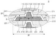
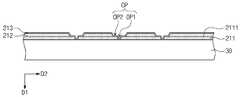
도 1, 도 2a 및 도 2b을 참조하면, 본 발명의 실시 예에 따른 반도체 패키지(1)는 반도체 칩(100), 몰딩 층(150), 재배선 기판(200) 및 외부 단자(300)를 포함할 수 있다.1, 2A and 2B , a
반도체 칩(100)은 재배선 기판(200)의 상면 상에 위치될 수 있다. 재배선 기판(200)의 상면(2112)은 반도체 칩(100)을 향한 면일 수 있다. 반도체 칩(100)은 그의 하면 상에 제공된 칩 패드들(110)과 패시베이션 층(passivation layer, 120)을 가질 수 있다. 반도체 칩(100)의 하면은 재배선 기판(200)을 향한 면일 수 있다. 패시베이션 층(120)은 반도체 칩(100)의 하면과 칩 패드들(110)을 덮을 수 있다. 패시베이션 층(120)은 칩 패드들(110)을 노출시키는 홀들(미부호)을 가질 수 있다. 반도체 칩(100)은 실리콘(Si)을 포함할 수 있다.The
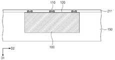
몰딩 층(150)은 재배선 기판(200)의 상면(2112) 상에 제공될 수 있다. 몰딩 층(150)은 반도체 칩(100)을 덮을 수 있다. 예를 들면, 몰딩 층(150)은 반도체 칩(100)의 상면과, 반도체 칩(100)의 측면을 덮을 수 있다. 반도체 칩(100)의 상면은 그의 하면으로부터 제1 방향(D1)으로 이격된 면일 수 있다. 몰딩 층(150)은 절연 물질, 예를 들면, 에폭시계 폴리머를 포함할 수 있다. 본 명세서에서, 제1 방향(D1)은 상하 방향과 평행할 수 있다.The
재배선 기판(200)은 반도체 칩(100)의 하면과 몰딩 층(150)의 하면 상에 제공될 수 있다. 몰딩 층(150)의 하면은 재배선 기판(200)을 향한 면일 수 있다. 재배선 기판(200)의 두께는 반도체 칩(100)의 두께보다 작을 수 있다. 재배선 기판(200)은 적어도 하나의 절연부를 포함할 수 있다. 절연부는 복수 개 제공될 수 있다. 실시 예에서, 재배선 기판(200)은 제1 절연부(210)와 제2 절연부(220)를 포함할 수 있다. 재배선 기판(200)은 제3 절연부(230)을 포함할 수 있다.The
제1 절연부(210)는 제1 절연 층(211), 제2 절연 층(212), 제1 재배선 도전 패턴(214) 및 제1 배리어 금속 층(213)을 포함할 수 있다. 제2 절연부(220)는 제3 절연 층(221), 제4 절연 층(222), 제2 재배선 도전 패턴(224) 및 제2 배리어 금속 층(223)을 포함할 수 있다.The first insulating
제1 및 제2 절연 층들(211, 212)은 서로 순차적으로 적층될 수 있다. 제1 및 제2 절연 층들(211, 212)은 경화성 물질을 포함할 수 있다. 이에 따라, 제1 및 제2 절연 층들(211, 212)은 열 또는 광에 의해 경화될 수 있다. 경화성 물질은 실리콘 산화물, 실리콘 질화물, 실리콘 산화질화물과 같은 무기 물질 및/또는 폴리아미드 계열의 고분자 물질을 포함하나, 이에 한정되지 않는다. 예를 들면, 경화성 물질은 감광성 폴리이미드(photosensitive polyimide, PSPI), 폴리벤조옥사졸(polybenzoxazole, PBO), 페놀계 폴리머(phenolic polymer), 벤조사이클로부텐인계(benzocyclobutene, BCB) 폴리머, 및 에폭시계 폴리머 중 적어도 하나를 포함할 수 있다. 실시 예에서, 제1 및 제2 절연 층들(211, 212)은 동일한 경화성 물질을 포함할 수 있다. 다른 예에서, 제1 및 제2 절연 층들(211, 212)은 상이한 경화성 물질을 포함할 수 있다.The first and second insulating
제1 절연 층(211)은 반도체 칩(100)의 하면 상에 위치될 수 있다. 예를 들면, 제1 절연 층(211)은 칩 패드(110)의 하면, 몰딩 층(150)의 하면, 및 패시베이션 층(120)의 하면을 덮을 수 있다. 제1 절연 층(211)은 서로 대향된 상면(2112)과 하면(2111)을 가질 수 있다. 실시 예에서, 제1 절연 층(211)의 상면(2112)은 재배선 기판(200)의 상면(2112)을 형성할 수 있다.The first insulating
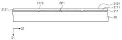
도 2a 및 도 4d를 참조하면, 제1 절연 층(211)은 그를 관통하는 제1 개구(OP1)를 포함할 수 있다. 제1 개구(OP1)는 칩 패드(110)를 노출할 수 있다. 또한, 제1 개구(OP1)는 제1 절연 층(211)의 제1 측벽(2113)을 노출할 수 있다. 제1 개구(OP1)은 제1 절연 층(211)에 복수 개 제공될 수 있다.2A and 4D , the first insulating
제2 절연 층(212)은 제1 절연 층(211)의 하면(2111) 상에 위치될 수 있다. 제1 절연 층(211)은 제2 절연 층(212)과 반도체 칩(100) 사이에 위치될 수 있다. 실시 예에서, 제2 절연 층(212)의 하면(2121)은 제3 절연 층(221)의 상면과 접할 수 있다.The second
제2 절연 층(212)은 그를 관통하는 제2 개구(OP2)를 가질 수 있다. 도 4f를 참조하면, 제2 개구(OP2)는 제1 절연 층(211)의 하면(2111)의 일부 및 제2 절연 층(212)의 제2 측벽(2123)을 노출할 수 있다. 제2 개구(OP2)의 일부는 제1 개구(OP1)과 수직하게 중첩될 수 있다. 제2 개구(OP2)의 폭(Width, W2)은 제1 개구(OP1)의 폭(W1)보다 크게 제공될 수 있다. 예를 들면, 제1 개구(OP1)는 평면적 관점에서, 제2 개구(OP2) 내에 위치될 수 있다. 제2 개구(OP2)는 제2 절연 층(212)에 복수 개 제공될 수 있다. 실시 예에서, 폭(Width)은 제1 방향(D1)과 수직한 제2 방향(D2)으로의 길이를 의미할 수 있다.The second
제1 개구(OP1)와 제2 개구(OP2)는 하나의 개구부(OP)를 형성할 수 있다. 제1 개구(OP1)와 제2 개구(OP2)는 동시에 형성될 수 있다. 예를 들면, 제1 개구(OP1)와 제2 개구(OP2)는 듀얼 다마신(dual damascene) 공정을 통해 제1 및 제2 절연 층들(211, 212)에 동시에 형성될 수 있다. 이에 대한, 자세한 설명은 후술한다.The first opening OP1 and the second opening OP2 may form one opening OP. The first opening OP1 and the second opening OP2 may be formed simultaneously. For example, the first opening OP1 and the second opening OP2 may be simultaneously formed in the first and second insulating
제1 배리어 금속 층(213)은 제1 재배선 도전 패턴들(214)과 제1 절연 층(211) 사이, 및 제1 재배선 도전 패턴들(214)과 제2 절연 층(212) 사이에 제공될 수 있다. 예를 들면, 제1 배리어 금속 층은 제1 절연 층(211)의 측벽(2113)과 제1 재배선 도전 패턴(214) 사이에 형성될 수 있다. 제1 배리어 금속 층(213)은 제2 절연 층(212)의 측벽(2123)과 제1 재배선 도전 패턴(214) 사이에 형성될 수 있다.The first
제1 배리어 금속 층(213)은 제1 개구(OP1) 및 제2 개구(OP2)에 의해 노출된 영역 상에 제공될 수 있다. 예를 들면, 제1 배리어 금속 층(213)은 제1 측벽(2113) 및 제2 측벽(2123) 상에 제공될 수 있다. 제1 배리어 금속 층(213)은 제1 개구(OP1)의 바닥부 상에 제공될 수 있다. 예를 들면, 제1 배리어 금속 층(213)은 제1 개구(OP1)에 의해 노출된 반도체 칩(100)의 칩 패드(110) 상에 제공될 수 있다. 제1 배리어 금속 층(213)은 제2 개구(OP2)에 의해 노출된 상기 하면(2111) 상에 제공될 수 있다. The first
제1 배리어 금속 층(213)은 금속 물질을 포함할 수 있다. 실시 예에서, 제1 배리어 금속 층(213)은 제1 개구(OP1) 및 제2 개구(OP2)에 의해 노출된 영역과, 제2 절연 층(212)의 하면(2121) 상에 금속 물질을 증착시켜 형성될 수 있다. 예를 들면, 제1 배리어 금속 층(213)은 Ta, TaN, TaSiN, Ti, TiN, TiSiN, W, 및 WN 중 적어도 하나를 포함할 수 있다. 또한, 제1 배리어 금속 층(213)은 약 5Å 내지 50 Å의 두께를 가질 수 있다.The first
제1 재배선 도전 패턴(214)은 제1 배리어 금속 층(213) 상에 제공될 수 있다. 제1 재배선 도전 패턴(214)들은 도전성 물질을 포함할 수 있다. 예를 들면, 제1 재배선 도전 패턴들(214)은 구리(Cu), 구리 합금 또는 알루미늄(Al)을 포함할 수 있다. 여기서, 구리 합금은 구리 내에 미량의 C, Ag, Co, Ta, In, Sn, Zn, Mn, Ti, Mg, Cr, Ge, Sr, Pt, Mg, Al 또는 Zr이 혼합된 것을 의미할 수 있다. 제1 재배선 도전 패턴(214)은 제1 및 제2 절연 층들(211, 212)에 제공될 수 있다. 제1 재배선 도전 패턴(214)은 칩 패드(110) 및/또는 제2 재배선 도전 패턴(224)과 전기적으로 연결될 수 있다.The first redistribution
제1 재배선 도전 패턴(214)은 서로 대향된 상면(2142)과 하면(2141)을 포함할 수 있다. 제1 재배선 도전 패턴(214)의 하면(2141)의 폭은 제1 재배선 도전 패턴(214)의 상면(2142)의 폭보다 클 수 있다. 제1 재배선 도전 패턴(214)의 상면(2142)은 제1 재배선 도전 패턴(214)의 하면(2141) 일부와 수직하게 중첩될 수 있다.The first redistribution
제1 재배선 도전 패턴(214)의 하면(2141) 및 노출된 제2 절연 층(212)의 하면(2121)은 서로 실질적으로 동일한 레벨을 가질 수 있다. 제1 재배선 도전 패턴(214)의 하면(2141)은 제2 절연 층(212)의 하면(2121)과 공면(coplanar)을 이룰 수 있다. 즉, 제1 재배선 도전 패턴(214)의 하면(2141)은 제2 절연 층(212)의 하면(2121)과 실질적으로 동일한 평면 상에 위치될 수 있다. 이에 따라, 제2 절연 층(212)의 하면(2121)과 제1 절연 층(211)의 하면(2111) 간의 수직 거리(H2), 및 제1 재배선 도전 패턴(214)의 하면(2141)과 제1 절연 층(211)의 하면(2111) 간의 수직 거리(H1)는 실질적으로 동일할 수 있다.The
도 2b에 도시된 바와 같이, 제1 재배선 도전 패턴(214)의 하면(2141)의 표면 거칠기(surface roughness)는 제2 절연 층(212)의 하면(2121)의 표면 거칠기보다 클 수 있다. 예를 들면, 제1 재배선 도전 패턴(214)의 하면(2141)의 표면 거칠기는 대략 약 0.01~0.5㎛이며, 아주 바람직하게는 약 0.086㎛이다. 제2 절연 층(212)의 하면(2121)의 표면 거칠기는 약 0.01~0.5㎛이며, 아주 바람직하게는 약 0.086㎛이다. 이에 따라, 제1 재배선 도전 패턴(214)의 하면(2141)과 제3 절연 층(221) 간의 접합력이 제2 절연 층(212)의 하면(2121)과 제3 절연 층(221) 간의 접합력보다 클 수 있다. 이에 따라, 제1 재배선 도전 패턴(214)과 제3 절연 층(221) 간의 이종 접합이 향상될 수 있다. 여기서, 이종 접합이란, 서로 다른 재질을 갖는 구성들을 접합하는 것을 의미할 수 있다.2B , the surface roughness of the
제1 재배선 도전 패턴(214)은 그의 하면(2141)과 상면(2142) 사이에 위치된 단차면(2144)을 포함할 수 있다. 제1 재배선 도전 패턴(214)는 그의 상면(2142)과 상기 단차면(2144)을 연결하는 제1 측면(2143)과, 그의 하면(2141)과 상기 단차면(2144)을 연결하는 제2 측면(2145)를 포함할 수 있다. 제1 재배선 도전 패턴(214)의 상면(2142), 하면(2141), 및 단차면(2144)은 실질적으로 서로 평행할 수 있다.The first redistribution
제2 측면(2145)의 폭은 제1 측면(2143)의 폭보다 클 수 있다. 제1 측면(2143)의 폭과 제2 측면(2145)의 폭은 제1 재배선 도전 패턴(214)의 상면(2142)으로부터 하면(2141)을 향해 갈수록 증가할 수 있다. 실시 예에서, 제1 측면(2143)과 제2 측면(2145)은 단차면(2144)과 경사진 경사면일 수 있다. 다른 예에서, 제1 측면(2143)과 제2 측면(2145)은 단차면(2144)과 실질적으로 수직할 수 있다. 제1 측면(2143)과 제2 측면(2145)은 실질적으로 서로 평행할 수 있으나, 이에 한정되지 않는다.A width of the
제1 및 제2 절연 층들(211, 212)과 제1 재배선 도전 패턴(214)의 열 팽창계수가 상이할 수 있다. 이에 따라, 제1 및 제2 절연 층들(211, 212)과 제1 재배선 도전 패턴(214) 간에 열적 스트레스(Thermal Stress)가 발생할 수 있다. 반도체 패키지는 제1 재배선 도전 패턴(214)의 제1 측면(2143) 및/또는 제2 측면들(2145)과 절연 층들 사이에 제1 배리어 금속 층(213)이 제공되지 않는 경우, 상기 열적 스트레스에 의해 제1 재배선 도전 패턴(214)의 제1 측면(2143) 및/또는 제2 측면들(2145) 상에 산화 층이 형성될 수 있다. 상기 산화 층에 의해 제1 재배선 도전 패턴(214)의 제1 측면(2143) 및/또는 제2 측면(2145)은 절연 층들에 대한 접착력이 저하될 수 있다. 즉, 제1 재배선 도전 패턴(214)의 제1 측면(2143) 및/또는 제2 측면(2145)이 절연 층들로부터 박리될 수 있다. 이에 따라, 반도체 패키지의 수명이 줄어들거나 파손될 수 있다.Coefficients of thermal expansion of the first and second insulating
본 발명의 실시 예에 따른, 반도체 패키지(1)는 제1 재배선 도전 패턴(214)의 제1 측면(2143)과 제1 절연 층(211) 사이에 제1 배리어 금속 층(213)이 제공될 수 있다. 또한, 반도체 패키지(1)는 제1 재배선 도전 패턴(214)의 제2 측면(2145)과 제2 절연 층(212) 사이에 제1 배리어 금속 층(213)이 제공될 수 있다. 제1 배리어 금속 층(213)은 상기 열적 스트레스에 의해 제1 재배선 도전 패턴(214)의 제1 및 제2 측면들(2143, 2145)의 박리 현상을 방지할 수 있다. 이에 따라, 반도체 패키지(1)의 수명이 향상되고, 파손 가능성이 줄어들 수 있다.According to an embodiment of the present invention, in the
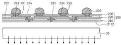
제2 절연부(220)는 제3 절연 층(221), 제4 절연 층(222), 제2 재배선 도전 패턴(224) 및 제2 배리어 금속 층(223)을 포함할 수 있다. 제2 절연부(220)는 제1 절연부(210)와 실질적으로 동일한 구성일 수 있다. 이에 따라, 제2 절연부(220)에 대한 설명은 제1 절연부(210)와의 차이점을 중심으로 설명한다.The second
제3 절연 층(221)은 제2 절연 층(212)의 하면(2121) 상에 제공될 수 있다. 제3 절연 층(221)은 그를 관통하는 제3 개구(OP3)를 포함할 수 있다. 제3 개구(OP3)는 복수 개 제공될 수 있다. 제3 개구(OP3)는 제1 재배선 도전 패턴(214)을 노출할 수 있다. 예를 들면, 제3 개구(OP3)는 제1 재배선 도전 패턴(214)의 하면(2141)의 일부를 노출할 수 있다. 제3 절연 층(221)은 제1 절연 층(211)과 실질적으로 동일한 구성일 수 있다.The third
제2 재배선 도전 패턴(224)은 제3 및 제4 절연 층들(221, 222) 사이에 개재될 수 있다. 제2 재배선 도전 패턴(224)는 제1 재배선 도전 패턴(214)과 전기적으로 접속될 수 있다. 본 명세서에서 접속한다는 것은 직접적인 접속 또는 다른 구성요소를 통한 간접적인 접속을 포함한다.The second redistribution
제3 절연부(230)는 제5 절연층(231), 제3 배리어 금속 층(233) 및 제3 재배선 도전 패턴(234)를 포함할 수 있다. 제3 절연부(230)는 제1 및 제2 절연부들(210, 220)과 달리, 하나의 절연 층을 포함할 수 있다. 제3 재배선 도전 패턴(234)은 제3 배리어 금속 층(233) 상에 위치될 수 있다.The third
제3 배리어 금속 층(233)은 제1 및 제2 배리어 금속 층들(213, 223)과 달리, 제5 절연 층(231)과 제3 재배선 도전 패턴(234) 사이에 위치될 수 있다. 제3 재배선 도전 패턴(234)는 제5 절연 층(231)으로부터 돌출된 구조일 수 있다. 즉, 제3 재배선 도전 패턴(234)의 측면의 일부에 제3 배리어 금속 층(233)이 형성되지 않을 수 있다. 제3 재배선 도전 패턴(234)는 제3 배리어 금속 층(233)을 통해 제2 재배선 도전 패턴(224)와 전기적으로 연결될 수 있다.Unlike the first and second
외부 단자들(300)은 재배선 기판(200)의 하면 상에 제공될 수 있다. 예를 들면, 외부 단자들(300)은 제3 재배선 도전 패턴(234) 상에 제공될 수 있다. 이에 따라, 재배선 기판(200)은 외부 단자들(300)과 반도체 칩(100) 사이에 위치될 수 있다. 외부 단자들(300)은 제3 재배선 도전 패턴(234)과 전기적으로 연결될 수 있다. 이에 따라, 외부 단자들(300)과 반도체 칩(100)은 제1 내지 제3 재배선 도전 패턴들(214, 224, 234)을 통해 전기적으로 접속될 수 있다.The
외부 단자들(300)의 각각은 솔더볼의 형상을 가질 수 있으나, 이에 한정되지 않는다. 외부 단자들(300) 중 일부는 반도체 칩(100)과 수직하게 중첩될 수 있다. 외부 단자들(300) 중 나머지는 반도체 칩(100)과 수직하게 중첩되지 않을 수 있다. 외부 단자들(300)의 일부는 평면적 관점에서 몰딩 층(150)과 중첩될 수 있다. 실시 예에서, 반도체 패키지(1)는 팬 아웃 패널 반도체 패키지(Fan-Out Package)일 수 있으나, 이에 한정되지 않는다.Each of the
도 3은 본 발명의 실시 예들에 따른 반도체 패키지의 변형 예를 나타낸 단면도이다. 설명의 간결함을 위해, 도 1, 도 2a 및 도 2b를 참조하여 참조하여 설명한 실시 예와 실질적으로 동일한 구성요소에 대한 설명은 생략하거나 간략히 설명한다.3 is a cross-sectional view illustrating a modified example of a semiconductor package according to embodiments of the present invention. For brevity of description, descriptions of components substantially the same as those of the embodiment described with reference to FIGS. 1, 2A, and 2B will be omitted or briefly described.
도 3을 참조하면, 반도체 패키지(2)는 제1 반도체 칩(100), 제2 반도체 칩(600), 제1 몰딩 층(150), 제2 몰딩 층(650), 연결 기판(400), 제1 재배선 기판(200), 및 제2 재배선 기판(500)을 포함할 수 있다. 반도체 패키지(2)는 제1 외부 단자들(300), 제2 외부 단자들(550) 및 연결 단자들(450)을 더 포함할 수 있다.Referring to FIG. 3 , the
제1 반도체 칩(100)은 제1 재배선 기판(200)의 상면 상에 위치될 수 있다. 제1 칩 패드(110) 및 제1 패시베이션 층(미도시)이 제1 반도체 칩(100)의 하면에 제공될 수 있다.The
연결 기판(400)은 제1 재배선 기판(200)의 상면 상에 위치될 수 있다. 연결 기판(400)은 제1 및 제2 재배선 기판들(200, 500) 사이에 위치될 수 있다. 평면적 관점에서, 연결 기판(400)은 제1 반도체 칩(100)의 측면을 둘러쌀 수 있다. 연결 기판(400)은 그를 관통하는 삽입 개구부(405)를 포함할 수 있다. 제1 반도체 칩(100)은 삽입 개구부(405) 내에 위치될 수 있다. 삽입 개구부(405)의 크기는 제1 반도체 칩(100)의 크기보다 클 수 있다. 이에 따라, 연결 기판(400)과 제1 반도체 칩(100) 간에 갭이 형성될 수 있다.The
연결 기판(400)은 베이스 층들(410)과 도전성 연결부(420)를 포함할 수 있다. 실시 예에서, 인쇄회로기판(PCB)이 연결 기판(400)으로 사용될 수 있다. 베이스 층들(410)은 비 도전성 물질을 포함할 수 있다. 예를 들면, 베이스 층들(410)은 탄소함유물질(예를 들어, 그라파이트 또는 그래핀), 세라믹, 또는 폴리머(예를 들면, 폴리카보네이트, 나일론, 또는 고밀도 폴리에틸렌(high-density polyethylene, HDPE))를 포함할 수 있다.The
도전성 연결부(420)는 제1 연결 패드들(421), 배선 패턴들(424), 제2 연결 패드들(423), 및 비아들(422)을 포함할 수 있다. 제1 연결 패드들(421)은 제1 재배선 기판(200) 상에 형성될 수 있다. 제1 연결 패드들(421)은 제1 재배선 도전 패턴들(214)과 전기적으로 접속될 수 있다. 제2 연결 패드들(423)은 연결 기판(400)의 상면에 제공될 수 있다. 비아들(422)은 베이스 층들(410)을 관통할 수 있다. 배선 패턴들(424)은 베이스 층들(410) 사이에 개재되며, 비아들(422)과 접속할 수 있다. 배선 패턴들(424)는 제1 및 제2 연결 패드들(421, 423) 사이에 위치될 수 있고, 비아들(422)을 통해 제1 및 제2 연결 패드들(421, 423)과 전기적으로 접속될 수 있다. 도전성 연결부(420)는 구리, 니켈, 알루미늄, 금, 은 스테인리스 스틸 또는 이들의 합금을 포함할 수 있다. 제1 연결 패드들(421), 제2 연결 패드들(423), 비아들(422) 및 배전 패턴들은 서로 수직하게 중첩될 수 있다.The
제1 재배선 기판(200)은 적어도 하나의 절연부를 포함할 수 있다. 실시 예에서, 제1 재배선 기판(200)은 제1 절연부(210), 제2 절연부(220), 및 제3 절연부(230)를 포함할 수 있다. 제1 절연부(210)는 제1 절연 층(211), 제2 절연 층(212), 제1 배리어 금속 층(213), 및 제1 재배선 도전 패턴(214)를 포함하고, 제2 절연부(220)는 제3 절연 층(221), 제4 절연 층(222), 제2 배리어 금속 층(223), 및 제2 재배선 도전 패턴(224)를 포함할 수 있다. 제3 절연부(230)는 제5 절연 층(231), 제3 배리어 금속 층(233), 및 제3 재배선 도전 패턴(234)를 포함할 수 있다. 제1 재배선 도전 패턴들(214)은 제1 칩 패드들(110)과, 제1 연결 패드들(421)과 접속할 수 있다.The
제1 외부 단자들(300)은 제1 재배선 기판(200)의 하면에 제공될 수 있다. 실시 예에서, 제1 외부 단자들(300)은 제3 재배선 도전 패턴(234)과 전기적으로 접속될 수 있다. 이에 따라, 제1 외부 단자들(300)은 제1 칩 패드들(110)과 제1 연결 패드들(421)과 전기적으로 접속될 수 있다.The first
제1 몰딩 층(150)이 연결 기판(400) 및 제1 반도체 칩(100) 상에 형성될 수 있다. 제1 몰딩 층(150)은 연결 기판(400)과 제1 반도체 칩(100) 사이의 갭에 제공될 수 있다. 제1 몰딩 층(150)은 제2 연결 패드들(423)을 노출시키는 개구들(미부호)을 포함할 수 있다.A
연결 단자들(450)은 제1 몰딩 층(150)의 개구들 내에 형성될 수 있다. 이에 따라, 연결 단자들(450)은 제2 연결 패드들(423)과 전기적으로 접속될 수 있다.The
제2 재배선 기판(500)은 제1 몰딩 층(150)의 상면에 형성될 수 있다. 제2 재배선 기판(500)은 적어도 하나의 절연부를 포함할 수 있다. 실시 예에서, 제2 재배선 기판(500)은 제4 절연부(510), 및 제5 절연부(520)를 포함할 수 있다. 제4 및 제5 절연부들(510, 520)은 제1 및 제2 절연부들(210, 220)과 실질적으로 동일한 구조로 형성될 수 있다. 제4 절연부(510)의 재배선 도전 패턴들(미부호)은 연결 단자들(450)과 접속할 수 있다. 제5 절연부(520)의 재배선 도전 패턴(미부호)들은 제4 절연부(510)의 재배선 도전 패턴들과 제2 외부 단자들과 전기적으로 접속될 수 있다.The
제2 반도체 칩(600)은 제2 재배선 기판(500) 상(over)에 제공될 수 있다. 제2 반도체 칩(600)의 하면에 제2 칩 패드들(610)이 제공될 수 있다.The
제2 외부 단자들(550)은 제2 반도체 칩(600)과 제2 재배선 기판(500) 사이에 위치될 수 있다. 제2 외부 단자들(550)은 제5 절연부(520)의 재배선 도전 패턴들과 제2 칩 패드들(610)과 전기적으로 접속될 수 있다.The second
제2 몰딩 층(650)은 제2 재배선 기판(500) 및 제2 반도체 칩(600)을 덮을 수 있다. 제2 몰딩 층(650)은 제1 몰딩 층(150)과 동일한 재질로 이루어질 수 있으나, 이에 한정되지 않는다.The
도 4a 내지 도 4l는 본 발명의 실시 예들에 따른 반도체 패키지의 제조 과정들을 나타낸 단면도들이다.4A to 4L are cross-sectional views illustrating manufacturing processes of a semiconductor package according to embodiments of the present invention.
도 4a를 참조하면, 지지 기판(20)이 준비될 수 있다. 지지 기판(20)은 그의 상면에 접착 층(25)이 제공될 수 있다. 복수의 반도체 칩들(100)이 지지 기판(20) 상에 위치될 수 있다. 반도체 칩들(100)은 제2 방향(D2)을 따라 배열될 수 있다. 반도체 칩들(100)은 서로 이격될 수 있다. 반도체 칩들(100)은 접착 층(25)에 의해 지지 기판(20)에 접착될 수 있다. 반도체 칩들(100)의 칩 패드들(110)과 패시베이션 층(120, 도 1 참조)은 지지 기판(20)과 마주볼 수 있다.Referring to FIG. 4A , the
도 4b를 참조하면, 지지 기판(20) 상에 반도체 칩들(100)을 덮는 몰딩 층(150)이 형성될 수 있다. 예를 들면, 절연 물질이 반도체 칩들(100)을 덮도록 지지 기판(20) 상에 공급될 수 있다. 이에 따라, 몰딩 층(150)이 지지 기판(20) 및 반도체 칩들(100) 상에 제공될 수 있다.Referring to FIG. 4B , a
도 4c 내지 도 4k는 복수의 반도체 칩들(100) 중 어느 하나를 중심으로 반도체 패키지 제조 과정을 설명하기로 한다. 도 4c를 참조하면, 지지 기판(20)을 반도체 칩들(100)과 몰딩 층(150)으로부터 제거할 수 있다. 이에 따라, 반도체 칩들(100)의 하면들과, 몰딩 층(150)의 하면이 노출될 수 있다. 또한, 반도체 칩들(100)과 몰딩 층(150)이 상하 반전될 수 있다.4C to 4K will describe a process of manufacturing a semiconductor package centering on any one of the plurality of
반도체 칩들(100)과 몰딩 층(150)을 상하 반전시킨 후, 예비 제1 절연 층(211')이 반도체 칩들(100)의 하면과 몰딩 층(150)의 하면에 형성될 수 있다. 예비 제1 절연 층(211')은 미 경화된 상태일 수 있다. 예를 들면, 미 경화된 제1 절연 층(211')이 칩 패드들(110), 패시베이션 층(120), 및 몰딩 층(150)의 하면을 덮을 수 있다. 예비 제1 절연 층(211')은 PECVD(Plasma Enhanced CVD), HDPCVD(High Density Plasma CVD), APCVD(Atmospheric Pressure CVD), 스핀 코팅(spin coating) 등을 이용하여 형성될 수 있다.After the
도 4d를 참조하면, 예비 제1 절연 층(211', 도 4c 참조)에 반도체 칩(100)을 노출하는 제1 개구들(OP1)을 형성할 수 있다. 예를 들면, 칩 패드들(110)을 노출시키는 제1 개구들(OP1)이 예비 제1 절연 층(211', 도 4c 참조)에 형성될 수 있다. 이에 따라, 반도체 칩(100)의 하면 상에 제1 개구들(OP1)을 포함하는 예비 제1 절연 층(211')이 형성될 수 있다.Referring to FIG. 4D , first openings OP1 exposing the
실시 예에서, 제1 개구들(OP1)은 예비 제1 절연 층(211') 상에 제1 마스크 패턴(미도시)을 형성하고, 제1 마스크 패턴을 이용하여 예비 제1 절연 층(211')을 식각함으로써 형성될 수 있다. 이에 따라, 예비 제1 절연 층(211')의 제1 측벽(2113)과 반도체 칩(100)의 칩 패드들(110)이 제1 개구들(OP1)를 통해 노출될 수 있다.In an embodiment, the first openings OP1 form a first mask pattern (not shown) on the preliminary first insulating
예비 제1 절연 층(211')은 후술할 제2 개구(OP2)가 형성되기 전에 경화될 수 있다. 실시 예에서, 제1 개구들(OP1)이 예비 제1 절연 층(211')에 형성된 후, 예비 제1 절연 층(211')은 열 또는 광에 의해 경화되어 제1 절연 층을 형성할 수 있다. 예를 들면, 제1 절연 층(211)은 약 150℃ 내지 약 200℃의 챔버(미도시) 내에 제공된 후, 상온(예를 들면, 약 25℃)으로 냉각되어 경화될 수 있다.The preliminary first insulating
도 4e를 참조하면, 제1 절연 층(211)의 하면(2111) 상에, 제1 개구들(OP1)을 채우는 예비 제2 절연 층(212')형성될 수 있다. 예비 제2 절연 층(212')은 미 경화된 상태일 수 있다. 예를 들면, 예비 제2 절연 층(212')은 제1 개구들(OP1)을 채우면서, 제1 절연 층(211)의 하면(2111)을 덮을 수 있다. 예비 제2 절연 층(212')은 PECVD(Plasma Enhanced CVD), HDPCVD(High Density Plasma CVD), APCVD(Atmospheric Pressure CVD), 스핀 코팅(spin coating) 등을 이용하여 형성될 수 있다.Referring to FIG. 4E , a preliminary second insulating
도 4f를 참조하면, 예비 제2 절연 층(212')에 제1 개구(OP1)와 중첩되는 제2 개구(OP2)를 형성할 수 있다. 예를 들면, 제2 개구(OP2)는 예비 제2 절연 층(212', 도 4e 참조) 상에 제2 마스크 패턴(미도시)을 형성하고, 제2 마스크 패턴을 이용하여 예비 제2 절연 층(212')들을 식각함으로써 형성될 수 있다. 제2 개구(OP2)를 형성하는 것은, 제1 절연 층(211)이 경화된 상태이고, 제2 절연 층(212)이 미 경화된 상태에서 수행될 수 있다. .Referring to FIG. 4F , a second opening OP2 overlapping the first opening OP1 may be formed in the preliminary second insulating
예비 제2 절연 층(212')에 제2 개구(OP2)가 형성되는 동안, 제1 개구(OP1) 내의 예비 제2 절연 층(212')이 제거될 수 있다. 이에 따라, 제1 개구(OP1)의 측벽이 노출될 수 있다. 실시 예에서, 제1 개구들(OP1)의 측벽은 제1 절연 층(211)의 측벽(2113)일 수 있다. 제1 개구(OP1)와 제2 개구(OP2)는 단일한 식각 공정에 의해 거의 동시에 형성될 수 있다. 이에 따라, 제1 절연부(210)에 개구부(OP)가 형성될 수 있다. 개구부(OP)는 제1 개구(OP1)과 제2 개구(OP2)를 포함할 수 있다.While the second opening OP2 is formed in the preliminary second insulating
제1 개구(OP1) 내의 예비 제2 절연 층(212')이 제거되고, 예비 제2 절연 층(212')에 제2 개구(OP2)가 형성된 후, 예비 제2 절연 층(212')은 경화될 수 있다. 즉, 제2 개구(OP2)가 형성된 예비 제2 절연 층(212')을 경화하여, 제2 절연 층(212)을 형성할 수 있다. 예를 들면, 제2 절연 층(212)은 약 150℃ 내지 약 200℃의 챔버(미도시) 내에 제공된 후, 상온(예를 들면, 약 25℃)으로 냉각되어 경화될 수 있다After the preliminary second insulating
칩 패드들(110), 제1 절연 층(211)의 제1 측벽(2113), 제1 절연 층(211)의 하면(2111)의 일부, 및 제2 절연 층(212)의 제2 측벽(2123)이 개구부(OP)에 의해 노출될 수 있다.The
도 4g를 참조하면, 제1 개구(OP1)의 측벽과 제2 개구(OP2)의 측벽을 따라서 제1 배리어 금속 층(213)을 형성할 수 있다. 제2 개구(OP2)의 측벽은 제2 절연 층(212)의 측벽(2123)일 수 있다. 예를 들면, 제1 배리어 금속 층(213)이 제1 및 제2 개구들(OP1, OP2)을 통해 노출된 칩 패드들(110), 제1 절연 층(211)의 하면(2111)의 일부, 제1 절연 층(211)의 제1 측벽(2113) 및 제2 절연 층(212)의 제2 측벽(2123) 상에 형성될 수 있다. 또한, 제1 배리어 금속 층(213)은 제2 절연 층(212)의 하면(2121)에 형성될 수 있다. 제1 배리어 금속 층(213)은 CVD(Chemical Vapor Deposition), ALD(Atomic Layer Deposition) 또는 스퍼터링과 같은 PVD(Physical Vapor Deposition) 방법을 이용하여 형성될 수 있다. 제1 배리어 금속 층(213)은 컨포멀(conformal)하게 형성될 수 있다.Referring to FIG. 4G , the first
도 4h를 참조하면, 제1 재배선 도전 패턴(214)이 제1 배리어 금속 층(213) 상에 형성될 수 있다. 예를 들면, 제1 재배선 도전 패턴(214)은 전기 도금법(electroplating) 또는 무전해 도금법(electroless plating)을 이용하여, 제1 배리어 금속 층(213) 상에 형성될 수 있다. 제1 재배선 도전 패턴(214)이 전기 도금법을 이용하여 제1 배리어 금속 층(213) 상에 형성될 때, 씨드 층(seed layer, 미도시)이 제1 배리어 금속 층(213)의 표면에 형성될 수 있다. 씨드 층은 도금 층의 균일성을 증가시키며 초기 핵 생성 자리(nucleation site) 역할을 할 수 있다. 제1 재배선 도전 패턴(214)은 제1 및 제2 개구들(OP1, OP2)을 채우면서, 제1 배리어 금속 층(213)을 덮을 수 있다. 제1 재배선 도전 패턴(214)는 제2 절연 층(212)의 하면(2121, 도 4f 참조) 상에 형성될 수 있다. 이에 따라, 제1 및 제2 개구들(OP1, OP2) 내에 차례로 제1 배리어 금속 층(213) 및 제1 재배선 도전 패턴(214)을 형성할 수 있다.Referring to FIG. 4H , a first redistribution
도 2b 및 도 4i를 참조하면, 평탄화 공정을 수행하여 제2 절연 층(212)의 하면(2121)을 노출할 수 있다. 제2 절연 층(212)의 하면(2121)과 제1 재배선 도전 패턴(214)의 하면(2141)이 평탄화 공정에 의해 실질적으로 동일 레벨에 위치될 수 있다. 즉, 제2 절연 층(212)의 하면(2121)과 제1 재배선 도전 패턴(214)의 하면(2141)이 평탄화 공정에 의해 공면(coplanar)을 이룰 수 있다. 여기서, 제2 절연 층(212)의 하면(2121)은 제2 절연 층(212)의 표면일 수 있고, 제1 재배선 도전 패턴(214)의 하면(2141)은 제1 재배선 도전 패턴(214)의 표면일 수 있다.2B and 4I , a planarization process may be performed to expose the
실시 예에서, 평탄화 공정은 제1 재배선 도전 패턴(214) 및/또는 제1 배리어 금속 층(213)을 식각하는 것일 수 있다. 예를 들면, 평탄화 공정은 화학적 식각 공정(chemical etching process)을 포함할 수 있다. 화학적 식각 공정이란, 제1 재배선 도전 패턴(214)의 표면 및/또는 제1 배리어 금속 층(213)의 표면을 약액을 사용하여 화학적으로 용해하여 제거하는 평탄화 기술일 수 있다. 다른 예에서, 평탄화 공정은 표면 컷팅(surface cutting) 공정을 포함할 수 있다. 표면 컷팅 공정이란, 제1 재배선 도전 패턴(214)의 표면 및/또는 제1 배리어 금속 층(213)의 표면을 블레이드를 이용하여 물리적으로 제거하는 평탄화 기술이다. 도 2b에 도시된 바와 같이, 평탄화 공정 후에 제1 재배선 도전 패턴(214)의 하면(2141)의 표면 거칠기(surface roughness)는 제2 절연 층(212)의 하면(2121)의 표면 거칠기보다 크게 형성될 수 있다.In an embodiment, the planarization process may be to etch the first redistribution
도 4j를 참조하면, 제2 절연부(220)가 제1 절연부(210) 상에 형성될 수 있다. 제2 절연부(220)는 도 4c 내지 도 4i에서 설명한 제1 절연부(210)의 형성 방법과 동일한 방법으로 형성될 수 있다. 다만, 제3 절연 층(221)이 제1 재배선 도전 패턴(214)의 하면(2141)과, 제2 절연 층(212)의 하면(2121) 상에 형성될 수 있다. 제3 절연 층(221)에 제공된 제3 개구들(OP3, 도 2a 참조)은 제1 재배선 도전 패턴(214)의 하면(2141)을 노출시킬 수 있다.Referring to FIG. 4J , the second insulating
도 4k를 참조하면, 제3 절연부(230)가 제2 절연부(220) 상에 형성될 수 있다. 실시 예에서, 제4 절연 층(222, 도 4j 참조)과, 제2 재배선 도전 패턴들(224, 도 4j 참조) 상에 예비 제5 절연 층이 형성될 수 있다.Referring to FIG. 4K , the third insulating
예비 제5 절연 층의 일부를 식각하여 개구를 형성할 수 있다. 예비 제54 절연 층의 개구는 제2 재배선 도전 패턴(224)를 노출시킬 수 있다. 예비 제5 절연 층은 경화될 수 있다. 경화된 제5 절연 층(231) 상에 상기 개구의 측벽을 따라서 제3 배리어 금속 층(233)을 형성할 수 있다. 상기 개구의 측벽은 제5 절연 층(231)의 측벽일 수 있다. 제3 배리어 금속 층(233)은 제5 절연 층(231)의 하면 상에 형성될 수 있다.An opening may be formed by etching a portion of the preliminary fifth insulating layer. The opening of the preliminary 54th insulating layer may expose the second redistribution
제3 배리어 금속 층(233)을 형성한 후, 제3 배리어 금속 층 상에 제3 마스크 패턴을 형성할 수 있다. 제3 재배선 도전 패턴(234)은 제3 마스크 패턴을 이용하여 제3 배리어 금속 층(233) 상에 형성될 수 있다. 제3 재배선 도전 패턴(234)는 제5 절연 층(231)의 개구를 채우면서, 제5 절연 층(231)으로부터 돌출된 구조로 이루어질 수 있다.After the third
제3 배리어 금속 층(233) 상에 제3 재배선 도전 패턴(234)을 형성한 후, 제3 마스크 패턴을 제거할 수 있다. 제3 마스크 패턴을 제거한 후, 제3 재배선 도전 패턴(234)과 중첩되지 않는 제3 배리어 금속 층(233)을 제거할 수 있다.After the third redistribution
제3 재배선 도전 패턴(234)과 중첩되지 않는 제3 배리어 금속 층(233)을 제거한 후, 재배선 기판(200)의 하면 상에 외부 단자들(300)을 형성할 수 있다. 예를 들면, 제3 재배선 도전 패턴들(234) 상에 외부 단자들(300)을 형성할 수 있다.After the third
도 4l를 참조하면, 재배선 기판(200)의 하면 상에 외부 단자들(300)이 형성된 후, 몰딩 층(150) 및 재배선 기판(200)을 절단하는 싱귤레이션(sigulation) 공정을 수행할 수 있다. 예를 들면, 도 4k에 도시된 점선을 따라, 몰딩 층(150) 및 재배선 기판(200)을 절단하여 단위 반도체 패키지들(1)로 분리할 수 있다.Referring to FIG. 4L , after
도 5a 내지 도 5i는 본 발명의 다른 실시 예들에 따른 반도체 패키지의 제조 과정들을 나타낸 단면도들이다. 도 5a 내지 도 5h는 단위 반도체 패키지를 중심으로 제조 과정들을 나타낸 것들이다. 설명의 편의를 위해 도 4a 내지 도 4k를 참조하여 설명한 실시 예와 실질적으로 동일한 구성 요소에 대한 설명은 생략하거나 간략히 설명한다.5A to 5I are cross-sectional views illustrating manufacturing processes of a semiconductor package according to other exemplary embodiments. 5A to 5H are views illustrating manufacturing processes based on a unit semiconductor package. For convenience of description, descriptions of components substantially the same as those of the embodiment described with reference to FIGS. 4A to 4K will be omitted or briefly described.
도 5a를 참조하면, 캐리어 기판(30) 상에 예비 제1 절연 층(211')을 형성할 수 있다. 캐리어 기판(30)을 노출하는 제1 개구들(OP1)을 예비 제1 절연 층(211') 상에 형성할 수 있다.Referring to FIG. 5A , a preliminary first insulating
도 5b를 참조하면, 예비 제1 절연 층(211', 도 5a 참조)은 열 또는 광에 의해 경화될 수 있다. 이에 따라, 캐리어 기판(30) 상에 캐리어 기판(30)을 노출하는 제1 개구(OP1)을 갖는 제1 절연 층(211)을 형성할 수 있다.Referring to FIG. 5B , the preliminary first insulating
제1 절연 층(211) 상에 제1 개구(OP1)를 채우는 예비 제2 절연 층(212')이 형성될 수 있다. 예를 들면, 예비 제2 절연 층(212')이 제1 개구들(OP1)을 채우면서 제1 절연 층(211)의 하면(2111)을 덮을 수 있다.A preliminary second insulating
도 5c를 참조하면, 예비 제2 절연 층(212', 도 5b 참조)에 제2 개구(OP2)를 형성할 수 있다. 예를 들면, 제1 개구(OP1) 내의 예비 제2 절연 층(212')을 제거하면서, 예비 제2 절연 층(212')에 제1 절연 층(211)의 하면(2111)을 노출하는 제2 개구(OP2)를 형성할 수 있다. 제2 개구(OP2)를 형성하는 동안 제1 개구(OP1)의 측벽이 노출될 수 있다. 제2 개구(OP2)를 형성하는 것은 제1 절연 층(211)이 경화된 상태이고, 예비 제2 절연 층(212')이 미 경화된 상태에서 수행될 수 있다. 제2 개구(OP2)를 형성한 후, 예비 제2 절연 층(212')을 경화시켜 제2 절연 층(212)을 형성할 수 있다.Referring to FIG. 5C , a second opening OP2 may be formed in the preliminary second insulating
제1 및 제2 개구들(OP1, OP2)는 캐리어 기판(30), 제1 절연 층(211)의 제1 측벽(2113), 제1 절연 층(211)의 하면(2111) 일부, 및 제2 절연 층(212)의 제2 측벽(2123)을 노출할 수 있다.The first and second openings OP1 and OP2 may include the
도 5d를 참조하면, 제1 및 제2 개구들(OP1, OP2)에 의해 노출된 캐리어 기판(30), 제1 측벽(2113, 도 5c 참조), 제1 절연 층(211)의 하면(2111), 및 제2 측벽(2123, 도 5c 참조) 상에 제1 배리어 금속 층(213)이 형성될 수 있다. 제1 배리어 금속 층(213)은 제2 절연 층(212)의 하면(2121, 도 5c 참조) 상에 형성될 수 있다.Referring to FIG. 5D , the
도 5e를 참조하면, 제1 재배선 도전 패턴(214)이 제1 배리어 금속 층(213) 상에 형성될 수 있다. 제1 재배선 도전 패턴(214)는 제2 절연 층(212)의 하면(2121, 도 5c 참조) 상(over)에 위치될 수 있다. 제1 재배선 도전 패턴(214)은 제1 및 제2 개구들(OP1, OP2)을 채우면서, 제1 배리어 금속 층(213)을 덮을 수 있다. 이에 따라, 제1 및 제2 개구들(OP1, OP2) 내에 차례로 제1 배리어 금속 층(213) 및 제1 재배선 도전 패턴(214)을 형성할 수 있다.Referring to FIG. 5E , a first redistribution
도 5f를 참조하면, 평탄화 공정을 수행하여 제2 절연 층(212)의 하면(2121)을 노출할 수 있다. 예를 들면, 평탄화 공정은 은 화학적 식각 공정을 포함할 수 있다. 이때, 평탄화 공정 후에 제1 재배선 도전 패턴(214)의 하면(2141)의 표면 거칠기는 제2 절연 층(212)의 하면(2121)의 표면 거칠기보다 클 수 있다(도 2b 참조).Referring to FIG. 5F , a planarization process may be performed to expose the
도 5g를 참조하면, 제2 절연부(220)가 제1 절연부(210) 상에 형성될 수 있다. 제2 절연부(220)는 도 5a 내지 도 5e에서 설명한 제1 절연부(210)의 형성 방법과 동일한 방법으로 형성될 수 있다. 제2 절연부(220) 상에 제3 절연부(230)를 형성할 수 있다(도 4k 참조). 이에 따라, 재배선 기판(200)이 형성될 수 있다.Referring to FIG. 5G , the second insulating
실시 예에서, 반도체 칩(100)이 재배선 기판(200)에 실장되기 전에 외부 단자들(300)이 재배선 기판(200)에 형성될 수 있다. 다른 예에서, 반도체 칩(100)이 재배선 기판에 실장된 후에 외부 단자들(300)이 재배선 기판(200)에 형성될 수 있다.In an embodiment, the
외부 단자들(300)이 제3 절연부(230)의 제3 재배선 도전 패턴들(234) 상에 형성될 수 있다. 이에 따라, 외부 단자들(300)은 제1 내지 제3 재배선 도전 패턴들(214, 224, 234)과 전기적으로 접속될 수 있다. 캐리어 기판(30)은 재배선 기판(200)으로부터 제거될 수 있다. 예를 들면, 캐리어 기판(30)은 제1 절연 층(211)으로부터 분리될 수 있다. 이에 따라, 재배선 기판(200)의 상면(예를 들면, 제1 절연 층(211)의 상면(2112))이 외부로 노출될 수 있다.
도 5h를 참조하면, 캐리어 기판(30)이 재배선 기판(200)으로부터 분리된 후, 재배선 기판(200)과 외부 단자들(300)이 상하 반전될 수 있다. 재배선 기판(200)이 상하 반전된 후, 재배선 기판(200)의 상면(2112) 상에 반도체 칩들(100)이 제공될 수 있다. 이때, 반도체 칩들(100)의 칩 패드들(110)은 제1 재배선 도전 패턴들(214)과 수직하게 중첩될 수 있다. 칩 패드들(110)은 도전성 연결 부재(130)에 의해 제1 재배선 도전 패턴들(214)과 전기적으로 연결될 수 있다. 도전성 연결 부재(130)는 솔더 볼, 필라 등일 수 있다. 실시 예에서, 도전성 연결 부재(130)는 칩 패드(110) 상에 제공될 수 있다. 또한, 반도체 칩(100)의 하면에 패시베이션 층(passivation layer, 120)이 제공될 수 있다. 패시베이션 층(120)은 칩 패드(110)를 노출하는 개구들을 가질 수 있고, 도전성 연결 부재(130)는 패시베이션 층(120)의 개구를 통해 칩 패드(110)와 전기적으로 접속할 수 있다. 도 5i를 참조하면, 반도체 칩들(100)이 위치된 재배선 기판(200)의 상면(2112) 상에 몰딩 층(150)이 형성될 수 있다. 몰딩 층(150)은 반도체 칩들(100)과 재배선 기판(200)의 상면을 덮을 수 있다. 몰딩 층(150)이 형성된 후, 싱귤레이션(sigulation) 공정을 진행하여, 도 5i에 도시된 점선을 따라, 몰딩 층(150) 및 재배선 기판(200)을 절단하여 단위 반도체 패키지들(1)로 분리할 수 있다.Referring to FIG. 5H , after the
이상에서는 본 발명의 바람직한 실시 예에 대하여 도시하고 설명하였지만, 본 발명은 상술한 특정의 실시 예에 한정되지 아니하며, 특허청구범위에서 청구하는 본 발명의 요지를 벗어남이 없이 당해 발명이 속하는 기술분야에서 통상의 지식을 가진 자에 의해 다양한 변형실시가 가능한 것은 물론이고, 이러한 변형실시들은 본 발명의 기술적 사상이나 전망으로부터 개별적으로 이해되어서는 안될 것이다.In the above, preferred embodiments of the present invention have been shown and described, but the present invention is not limited to the specific embodiments described above, and without departing from the gist of the present invention as claimed in the claims, in the technical field to which the present invention pertains. Various modifications may be made by those of ordinary skill in the art, and these modifications should not be individually understood from the technical spirit or perspective of the present invention.
Claims (10)
Translated fromKorean상기 예비 제1 절연 층을 경화하여, 제1 절연 층을 형성하는 것;
상기 제1 절연 층 상에, 상기 제1 개구를 채우는 예비 제2 절연 층을 형성하는 것;
상기 예비 제2 절연 층에 상기 제1 개구와 중첩되는 제2 개구를 형성하는 것, 상기 제2 개구를 형성하는 동안 상기 제1 개구의 측벽이 노출되고;
상기 제2 개구가 형성된 상기 예비 제2 절연 층을 경화하여, 제2 절연 층을 형성하는 것;
상기 제1 개구의 측벽과 상기 제2 개구의 측벽을 따라서 배리어 금속 층을 형성하는 것;
상기 배리어 금속 층 상에 재배선 도전 패턴을 형성하는 것; 및
평탄화 공정을 수행하여 상기 제2 절연 층을 노출하는 것을 포함하는 반도체 패키지의 제조 방법.forming a preliminary first insulating layer comprising a first opening;
curing the preliminary first insulating layer to form a first insulating layer;
forming a preliminary second insulating layer filling the first opening on the first insulating layer;
forming a second opening overlapping the first opening in the preliminary second insulating layer, wherein a sidewall of the first opening is exposed while forming the second opening;
curing the preliminary second insulating layer in which the second opening is formed to form a second insulating layer;
forming a barrier metal layer along a sidewall of the first opening and a sidewall of the second opening;
forming a redistribution conductive pattern on the barrier metal layer; and
and exposing the second insulating layer by performing a planarization process.
상기 평탄화 공정 후에 상기 재배선 도전 패턴의 표면 거칠기(surface roughness)는 상기 제2 절연 층의 표면 거칠기(surface roughness)보다 큰 반도체 패키지의 제조 방법.According to claim 1,
After the planarization process, a surface roughness of the redistribution conductive pattern is greater than a surface roughness of the second insulating layer.
상기 평탄화 공정은 화학적 식각 공정을 포함하는 반도체 패키지의 제조 방법.According to claim 1,
The planarization process is a method of manufacturing a semiconductor package including a chemical etching process.
상기 제2 개구의 폭은 상기 제1 개구의 폭보다 큰 반도체 패키지의 제조 방법.According to claim 1,
A width of the second opening is greater than a width of the first opening.
상기 평탄화 공정에 의해 상기 재배선 도전 패턴의 표면, 및 상기 제2 절연 층의 표면은 공면(coplanar)을 이루는 반도체 패키지의 제조 방법.According to claim 1,
A method of manufacturing a semiconductor package in which a surface of the redistribution conductive pattern and a surface of the second insulating layer are coplanar by the planarization process.
상기 제1 절연 층과 상기 제2 절연 층은 감광성 폴리이미드(photosensitive polyimide, PSPI), 폴리벤조옥사졸(polybenzoxazole, PBO), 페놀계 폴리머(phenolic polymer), 및 benzocyclobutene계 폴리머(BCB) 중 적어도 하나를 포함하는 반도체 패키지의 제조 방법.According to claim 1,
The first insulating layer and the second insulating layer are at least one of a photosensitive polyimide (PSPI), polybenzoxazole (PBO), a phenolic polymer, and a benzocyclobutene-based polymer (BCB). A method of manufacturing a semiconductor package comprising a.
상기 제1 절연 층 상에, 상기 제1 개구를 채우는 제2 절연 층을 형성하는 것;
상기 제2 절연 층에 상기 제1 개구와 중첩되는 제2 개구를 형성하는 것, 상기 제2 개구를 형성하는 동안 상기 제1 개구의 측벽이 노출되고;
상기 제1 및 제2 개구들 내에 차례로 배리어 금속 층 및 재배선 도전 패턴을 형성하는 것; 및
평탄화 공정을 수행하여 상기 제2 절연 층을 노출하는 것을 포함하되,
상기 제2 개구를 형성하는 것은, 상기 제1 절연 층이 경화된 상태이고, 상기 제2 절연 층이 미 경화된 상태에서 수행되는 반도체 패키지의 제조 방법.forming a first insulating layer on the semiconductor chip, the first insulating layer having a first opening exposing the semiconductor chip;
forming a second insulating layer filling the first opening on the first insulating layer;
forming a second opening in the second insulating layer overlapping the first opening, wherein a sidewall of the first opening is exposed while forming the second opening;
sequentially forming a barrier metal layer and a redistribution conductive pattern in the first and second openings; and
performing a planarization process to expose the second insulating layer;
The forming of the second opening is performed when the first insulating layer is in a cured state and the second insulating layer is in an uncured state.
상기 평탄화 공정 후에 상기 재배선 도전 패턴의 표면 거칠기(surface roughness)는 상기 제2 절연 층의 표면 거칠기(surface roughness)보다 큰 반도체 패키지의 제조 방법.8. The method of claim 7,
After the planarization process, a surface roughness of the redistribution conductive pattern is greater than a surface roughness of the second insulating layer.
상기 재배선 기판 상에 반도체 칩을 제공하여, 상기 반도체 칩을 상기 재배선 기판과 전기적으로 연결시키는 것을 포함하되,
상기 재배선 기판을 형성하는 것은:
캐리어 기판 상에 상기 캐리어 기판을 노출하는 제1 개구를 갖는 제1 절연 층을 형성하는 것;
상기 제1 절연 층 상에, 상기 제1 개구를 채우는 제2 절연 층을 형성하는 것;
상기 제2 절연 층에 제2 개구를 형성하는 것, 상기 제2 개구를 형성하는 동안 상기 제1 개구의 측벽이 노출되고;
상기 제1 및 제2 개구들 내에 차례로 배리어 금속 층 및 재배선 도전 패턴을 형성하는 것; 및
평탄화 공정을 수행하여 상기 제2 절연 층을 노출하는 것을 포함하되,
상기 제2 개구를 형성하는 것은 상기 제1 절연 층이 경화된 상태이고, 상기 제2 절연 층이 미 경화된 상태에서 수행되는 반도체 패키지의 제조 방법.forming a redistribution substrate; and
providing a semiconductor chip on the redistribution substrate to electrically connect the semiconductor chip to the redistribution substrate;
Forming the redistribution substrate includes:
forming a first insulating layer on the carrier substrate, the first insulating layer having a first opening exposing the carrier substrate;
forming a second insulating layer filling the first opening on the first insulating layer;
forming a second opening in the second insulating layer, wherein a sidewall of the first opening is exposed while forming the second opening;
sequentially forming a barrier metal layer and a redistribution conductive pattern in the first and second openings; and
performing a planarization process to expose the second insulating layer;
The forming of the second opening is performed when the first insulating layer is in a cured state and the second insulating layer is in an uncured state.
평탄화 공정 후에 상기 재배선 도전 패턴의 표면 거칠기(surface roughness)는 상기 제2 절연 층의 표면 거칠기(surface roughness)보다 큰 반도체 패키지의 제조 방법.10. The method of claim 9,
After the planarization process, a surface roughness of the redistribution conductive pattern is greater than a surface roughness of the second insulating layer.
Priority Applications (4)
| Application Number | Priority Date | Filing Date | Title |
|---|---|---|---|
| KR1020170097251AKR102459308B1 (en) | 2017-07-31 | 2017-07-31 | Method for fabricating semiconductor package |
| US15/867,075US10546829B2 (en) | 2017-07-31 | 2018-01-10 | Method of fabricating semiconductor package |
| US16/698,117US10741518B2 (en) | 2017-07-31 | 2019-11-27 | Method of fabricating semiconductor package |
| US16/914,384US11018108B2 (en) | 2017-07-31 | 2020-06-28 | Method of fabricating semiconductor package |
Applications Claiming Priority (1)
| Application Number | Priority Date | Filing Date | Title |
|---|---|---|---|
| KR1020170097251AKR102459308B1 (en) | 2017-07-31 | 2017-07-31 | Method for fabricating semiconductor package |
Publications (2)
| Publication Number | Publication Date |
|---|---|
| KR20190014271A KR20190014271A (en) | 2019-02-12 |
| KR102459308B1true KR102459308B1 (en) | 2022-10-31 |
Family
ID=65039037
Family Applications (1)
| Application Number | Title | Priority Date | Filing Date |
|---|---|---|---|
| KR1020170097251AActiveKR102459308B1 (en) | 2017-07-31 | 2017-07-31 | Method for fabricating semiconductor package |
Country Status (2)
| Country | Link |
|---|---|
| US (3) | US10546829B2 (en) |
| KR (1) | KR102459308B1 (en) |
Families Citing this family (7)
| Publication number | Priority date | Publication date | Assignee | Title |
|---|---|---|---|---|
| KR102459308B1 (en) | 2017-07-31 | 2022-10-31 | 삼성전자주식회사 | Method for fabricating semiconductor package |
| KR102513085B1 (en)* | 2018-11-20 | 2023-03-23 | 삼성전자주식회사 | Fan-out semiconductor package |
| US11158607B2 (en)* | 2018-11-29 | 2021-10-26 | Apple Inc. | Wafer reconstitution and die-stitching |
| KR102741113B1 (en)* | 2020-01-21 | 2024-12-10 | 삼성전자주식회사 | Semiconductor package-and-package on package having the same |
| KR102759371B1 (en)* | 2020-02-18 | 2025-01-24 | 삼성전자주식회사 | Semiconductor package-and-package on package having the same |
| KR20220126320A (en) | 2021-03-08 | 2022-09-16 | 삼성전자주식회사 | semiconductor package |
| US20240112969A1 (en)* | 2022-08-31 | 2024-04-04 | Industrial Technology Research Institute | In-mold electronics device |
Citations (2)
| Publication number | Priority date | Publication date | Assignee | Title |
|---|---|---|---|---|
| US20150034374A1 (en) | 2013-07-30 | 2015-02-05 | Ibiden Co., Ltd. | Printed wiring board and method for manufacturing printed wiring board |
| US20160224811A1 (en) | 2015-02-03 | 2016-08-04 | KYOCERA Circuit Solutions, Inc. | Wiring board and method for recognizing code information thereof |
Family Cites Families (15)
| Publication number | Priority date | Publication date | Assignee | Title |
|---|---|---|---|---|
| MY139405A (en)* | 1998-09-28 | 2009-09-30 | Ibiden Co Ltd | Printed circuit board and method for its production |
| US7405149B1 (en) | 1998-12-21 | 2008-07-29 | Megica Corporation | Post passivation method for semiconductor chip or wafer |
| US6762115B2 (en) | 1998-12-21 | 2004-07-13 | Megic Corporation | Chip structure and process for forming the same |
| EP1818975A3 (en)* | 2000-02-25 | 2010-09-29 | Ibiden Co., Ltd. | Multilayer printed circuit board and multilayer printed circuit board manufacturing method |
| KR100394808B1 (en) | 2001-07-19 | 2003-08-14 | 삼성전자주식회사 | Wafer level stack chip package and method for manufacturing the same |
| JP2003045877A (en)* | 2001-08-01 | 2003-02-14 | Sharp Corp | Semiconductor device and method of manufacturing the same |
| US8349658B2 (en)* | 2010-05-26 | 2013-01-08 | Stats Chippac, Ltd. | Semiconductor device and method of forming conductive posts and heat sink over semiconductor die using leadframe |
| US8803306B1 (en) | 2013-01-18 | 2014-08-12 | Taiwan Semiconductor Manufacturing Company, Ltd. | Fan-out package structure and methods for forming the same |
| KR20140111523A (en) | 2013-03-11 | 2014-09-19 | 삼성전자주식회사 | Semiconductor package and method for fabricating the same |
| US9502365B2 (en)* | 2013-12-31 | 2016-11-22 | Texas Instruments Incorporated | Opening in a multilayer polymeric dielectric layer without delamination |
| JP6437246B2 (en) | 2014-08-28 | 2018-12-12 | ルネサスエレクトロニクス株式会社 | Semiconductor device and manufacturing method thereof |
| US9583462B2 (en) | 2015-01-22 | 2017-02-28 | Qualcomm Incorporated | Damascene re-distribution layer (RDL) in fan out split die application |
| US11018025B2 (en)* | 2015-07-31 | 2021-05-25 | Taiwan Semiconductor Manufacturing Company, Ltd. | Redistribution lines having stacking vias |
| US10304700B2 (en)* | 2015-10-20 | 2019-05-28 | Taiwan Semiconductor Manufacturing Company, Ltd. | Semiconductor device and method |
| KR102459308B1 (en) | 2017-07-31 | 2022-10-31 | 삼성전자주식회사 | Method for fabricating semiconductor package |
- 2017
- 2017-07-31KRKR1020170097251Apatent/KR102459308B1/enactiveActive
- 2018
- 2018-01-10USUS15/867,075patent/US10546829B2/enactiveActive
- 2019
- 2019-11-27USUS16/698,117patent/US10741518B2/enactiveActive
- 2020
- 2020-06-28USUS16/914,384patent/US11018108B2/enactiveActive
Patent Citations (2)
| Publication number | Priority date | Publication date | Assignee | Title |
|---|---|---|---|---|
| US20150034374A1 (en) | 2013-07-30 | 2015-02-05 | Ibiden Co., Ltd. | Printed wiring board and method for manufacturing printed wiring board |
| US20160224811A1 (en) | 2015-02-03 | 2016-08-04 | KYOCERA Circuit Solutions, Inc. | Wiring board and method for recognizing code information thereof |
Also Published As
| Publication number | Publication date |
|---|---|
| KR20190014271A (en) | 2019-02-12 |
| US10741518B2 (en) | 2020-08-11 |
| US20190035756A1 (en) | 2019-01-31 |
| US20200098716A1 (en) | 2020-03-26 |
| US20200328175A1 (en) | 2020-10-15 |
| US11018108B2 (en) | 2021-05-25 |
| US10546829B2 (en) | 2020-01-28 |
Similar Documents
| Publication | Publication Date | Title |
|---|---|---|
| KR102459308B1 (en) | Method for fabricating semiconductor package | |
| US11270965B2 (en) | Semiconductor device with thin redistribution layers | |
| US12062588B2 (en) | Semiconductor package having routable encapsulated conductive substrate and method | |
| US10446526B2 (en) | Face-to-face semiconductor assembly having semiconductor device in dielectric recess | |
| TWI700794B (en) | Integrated fan-out package and method of fabricating the same | |
| US10985138B2 (en) | Semiconductor package having a plurality of chips and method of manufacturing the same | |
| US9230901B2 (en) | Semiconductor device having chip embedded in heat spreader and electrically connected to interposer and method of manufacturing the same | |
| TWI711056B (en) | Conductive pattern | |
| KR20200134377A (en) | Semiconductor Package | |
| US11721577B2 (en) | Semiconductor package and method of manufacturing the same | |
| TW201801271A (en) | Semiconductor device | |
| KR20230000798A (en) | semiconductor package and method of manufacturing the same | |
| US20210028144A1 (en) | Semiconductor device package and method of manufacturing the same | |
| KR20220009193A (en) | Semiconductor pacakge device | |
| US11948899B2 (en) | Semiconductor substrate structure and manufacturing method thereof | |
| TW201637147A (en) | A semiconductor package using a contact in a plated sidewall encapsulant opening | |
| KR20080045017A (en) | Semiconductor chip package having metal bumps and manufacturing method thereof | |
| CN116387169B (en) | Packaging method and packaging structure | |
| CN112466829A (en) | Chip packaging structure and preparation method thereof | |
| TW202111886A (en) | Package structure and method of forming the same | |
| CN101937901B (en) | Circuit substrate and its manufacturing method and packaging structure | |
| KR20230033362A (en) | Semiconductor package and method for manufacturing of the same | |
| CN220155524U (en) | semiconductor structure |
Legal Events
| Date | Code | Title | Description |
|---|---|---|---|
| PA0109 | Patent application | St.27 status event code:A-0-1-A10-A12-nap-PA0109 | |
| PG1501 | Laying open of application | St.27 status event code:A-1-1-Q10-Q12-nap-PG1501 | |
| A201 | Request for examination | ||
| PA0201 | Request for examination | St.27 status event code:A-1-2-D10-D11-exm-PA0201 | |
| D18-X000 | Deferred examination requested | St.27 status event code:A-1-2-D10-D18-exm-X000 | |
| D19-X000 | Deferred examination accepted | St.27 status event code:A-1-2-D10-D19-exm-X000 | |
| E701 | Decision to grant or registration of patent right | ||
| PE0701 | Decision of registration | St.27 status event code:A-1-2-D10-D22-exm-PE0701 | |
| D20-X000 | Deferred examination resumed | St.27 status event code:A-1-2-D10-D20-exm-X000 | |
| PR0701 | Registration of establishment | St.27 status event code:A-2-4-F10-F11-exm-PR0701 | |
| PR1002 | Payment of registration fee | St.27 status event code:A-2-2-U10-U11-oth-PR1002 Fee payment year number:1 | |
| PG1601 | Publication of registration | St.27 status event code:A-4-4-Q10-Q13-nap-PG1601 | |
| PR1001 | Payment of annual fee | St.27 status event code:A-4-4-U10-U11-oth-PR1001 Fee payment year number:4 |