KR102456428B1 - Display Device having white sub-pixel and Method of Driving the same - Google Patents
Display Device having white sub-pixel and Method of Driving the sameDownload PDFInfo
- Publication number
- KR102456428B1 KR102456428B1KR1020150150500AKR20150150500AKR102456428B1KR 102456428 B1KR102456428 B1KR 102456428B1KR 1020150150500 AKR1020150150500 AKR 1020150150500AKR 20150150500 AKR20150150500 AKR 20150150500AKR 102456428 B1KR102456428 B1KR 102456428B1
- Authority
- KR
- South Korea
- Prior art keywords
- pixel
- data
- sub
- dark dot
- dark
- Prior art date
- Legal status (The legal status is an assumption and is not a legal conclusion. Google has not performed a legal analysis and makes no representation as to the accuracy of the status listed.)
- Active
Links
Images


Classifications
- G—PHYSICS
- G09—EDUCATION; CRYPTOGRAPHY; DISPLAY; ADVERTISING; SEALS
- G09G—ARRANGEMENTS OR CIRCUITS FOR CONTROL OF INDICATING DEVICES USING STATIC MEANS TO PRESENT VARIABLE INFORMATION
- G09G3/00—Control arrangements or circuits, of interest only in connection with visual indicators other than cathode-ray tubes
- G09G3/20—Control arrangements or circuits, of interest only in connection with visual indicators other than cathode-ray tubes for presentation of an assembly of a number of characters, e.g. a page, by composing the assembly by combination of individual elements arranged in a matrix no fixed position being assigned to or needed to be assigned to the individual characters or partial characters
- G09G3/2003—Display of colours
- G—PHYSICS
- G09—EDUCATION; CRYPTOGRAPHY; DISPLAY; ADVERTISING; SEALS
- G09G—ARRANGEMENTS OR CIRCUITS FOR CONTROL OF INDICATING DEVICES USING STATIC MEANS TO PRESENT VARIABLE INFORMATION
- G09G3/00—Control arrangements or circuits, of interest only in connection with visual indicators other than cathode-ray tubes
- G09G3/20—Control arrangements or circuits, of interest only in connection with visual indicators other than cathode-ray tubes for presentation of an assembly of a number of characters, e.g. a page, by composing the assembly by combination of individual elements arranged in a matrix no fixed position being assigned to or needed to be assigned to the individual characters or partial characters
- G09G3/22—Control arrangements or circuits, of interest only in connection with visual indicators other than cathode-ray tubes for presentation of an assembly of a number of characters, e.g. a page, by composing the assembly by combination of individual elements arranged in a matrix no fixed position being assigned to or needed to be assigned to the individual characters or partial characters using controlled light sources
- G09G3/30—Control arrangements or circuits, of interest only in connection with visual indicators other than cathode-ray tubes for presentation of an assembly of a number of characters, e.g. a page, by composing the assembly by combination of individual elements arranged in a matrix no fixed position being assigned to or needed to be assigned to the individual characters or partial characters using controlled light sources using electroluminescent panels
- G09G3/32—Control arrangements or circuits, of interest only in connection with visual indicators other than cathode-ray tubes for presentation of an assembly of a number of characters, e.g. a page, by composing the assembly by combination of individual elements arranged in a matrix no fixed position being assigned to or needed to be assigned to the individual characters or partial characters using controlled light sources using electroluminescent panels semiconductive, e.g. using light-emitting diodes [LED]
- G09G3/3208—Control arrangements or circuits, of interest only in connection with visual indicators other than cathode-ray tubes for presentation of an assembly of a number of characters, e.g. a page, by composing the assembly by combination of individual elements arranged in a matrix no fixed position being assigned to or needed to be assigned to the individual characters or partial characters using controlled light sources using electroluminescent panels semiconductive, e.g. using light-emitting diodes [LED] organic, e.g. using organic light-emitting diodes [OLED]
- G09G3/3225—Control arrangements or circuits, of interest only in connection with visual indicators other than cathode-ray tubes for presentation of an assembly of a number of characters, e.g. a page, by composing the assembly by combination of individual elements arranged in a matrix no fixed position being assigned to or needed to be assigned to the individual characters or partial characters using controlled light sources using electroluminescent panels semiconductive, e.g. using light-emitting diodes [LED] organic, e.g. using organic light-emitting diodes [OLED] using an active matrix
- G09G3/3233—Control arrangements or circuits, of interest only in connection with visual indicators other than cathode-ray tubes for presentation of an assembly of a number of characters, e.g. a page, by composing the assembly by combination of individual elements arranged in a matrix no fixed position being assigned to or needed to be assigned to the individual characters or partial characters using controlled light sources using electroluminescent panels semiconductive, e.g. using light-emitting diodes [LED] organic, e.g. using organic light-emitting diodes [OLED] using an active matrix with pixel circuitry controlling the current through the light-emitting element
- G—PHYSICS
- G09—EDUCATION; CRYPTOGRAPHY; DISPLAY; ADVERTISING; SEALS
- G09G—ARRANGEMENTS OR CIRCUITS FOR CONTROL OF INDICATING DEVICES USING STATIC MEANS TO PRESENT VARIABLE INFORMATION
- G09G5/00—Control arrangements or circuits for visual indicators common to cathode-ray tube indicators and other visual indicators
- G09G5/02—Control arrangements or circuits for visual indicators common to cathode-ray tube indicators and other visual indicators characterised by the way in which colour is displayed
- G—PHYSICS
- G09—EDUCATION; CRYPTOGRAPHY; DISPLAY; ADVERTISING; SEALS
- G09G—ARRANGEMENTS OR CIRCUITS FOR CONTROL OF INDICATING DEVICES USING STATIC MEANS TO PRESENT VARIABLE INFORMATION
- G09G2300/00—Aspects of the constitution of display devices
- G09G2300/04—Structural and physical details of display devices
- G09G2300/0439—Pixel structures
- G09G2300/0452—Details of colour pixel setup, e.g. pixel composed of a red, a blue and two green components
- G—PHYSICS
- G09—EDUCATION; CRYPTOGRAPHY; DISPLAY; ADVERTISING; SEALS
- G09G—ARRANGEMENTS OR CIRCUITS FOR CONTROL OF INDICATING DEVICES USING STATIC MEANS TO PRESENT VARIABLE INFORMATION
- G09G2300/00—Aspects of the constitution of display devices
- G09G2300/08—Active matrix structure, i.e. with use of active elements, inclusive of non-linear two terminal elements, in the pixels together with light emitting or modulating elements
- G09G2300/0809—Several active elements per pixel in active matrix panels
- G09G2300/0842—Several active elements per pixel in active matrix panels forming a memory circuit, e.g. a dynamic memory with one capacitor
- G—PHYSICS
- G09—EDUCATION; CRYPTOGRAPHY; DISPLAY; ADVERTISING; SEALS
- G09G—ARRANGEMENTS OR CIRCUITS FOR CONTROL OF INDICATING DEVICES USING STATIC MEANS TO PRESENT VARIABLE INFORMATION
- G09G2320/00—Control of display operating conditions
- G09G2320/02—Improving the quality of display appearance
- G09G2320/0242—Compensation of deficiencies in the appearance of colours
Landscapes
- Engineering & Computer Science (AREA)
- Physics & Mathematics (AREA)
- Computer Hardware Design (AREA)
- General Physics & Mathematics (AREA)
- Theoretical Computer Science (AREA)
- Control Of Indicators Other Than Cathode Ray Tubes (AREA)
Abstract
Translated fromKoreanDescription
Translated fromKorean본 발명은 백색 서브 픽셀을 가지는 표시장치와 그 구동 방법에 관한 것이다.The present invention relates to a display device having a white sub-pixel and a driving method thereof.
액정표시장치(Liquid Crystal Display Device: LCD), 유기 발광 다이오드 표시장치(Organic Light Emitting Diode Display : 이하 “OLED 표시장치”라 함), 플라즈마 디스플레이 패널(Plasma Display Panel : PDP), 전기영동 표시장치(Electrophoretic Display Device: EPD) 등 각종 평판 표시장치가 개발되고 있다. 액정표시장치는 액정 분자에 인가되는 전계를 데이터 전압에 따라 제어하여 화상을 표시한다. 액티브 매트릭스(Active Matrix) 구동방식의 표시장치에는 픽셀 마다 박막트랜지스터(Thin Film Transistor : 이하 "TFT"라 함)가 형성되어 있다.Liquid Crystal Display Device (LCD), Organic Light Emitting Diode Display (hereinafter referred to as “OLED Display Device”), Plasma Display Panel (PDP), Electrophoretic Display ( Various flat panel display devices such as Electrophoretic Display Device (EPD) are being developed. A liquid crystal display displays an image by controlling an electric field applied to liquid crystal molecules according to a data voltage. In an active matrix driving type display device, a thin film transistor (hereinafter, referred to as “TFT”) is formed for each pixel.
액티브 매트릭스 타입의 OLED 표시장치는 스스로 발광하는 유기 발광다이오드(Organic Light Emitting Diode: 이하, "OLED"라 함)를 포함하며, 응답속도가 빠르고 발광효율, 휘도 및 시야각이 큰 장점이 있다. OLED는 애노드와 캐소드 사이에 형성된 유기 화합물층을 포함한다. 유기 화합물층은 정공주입층(Hole Injection layer, HIL), 정공수송층(Hole transport layer, HTL), 발광층(Emission layer, EML), 전자수송층(Electron transport layer, ETL) 및 전자주입층(Electron Injection layer, EIL)으로 이루어진다. 애노드전극과 캐소드전극에 구동전압이 인가되면 정공수송층(HTL)을 통과한 정공과 전자수송층(ETL)을 통과한 전자가 발광층(EML)으로 이동되어 여기자를 형성하고, 그 결과 발광층(EML)이 가시광을 발생하게 된다.The active matrix type OLED display includes an organic light emitting diode (hereinafter, referred to as "OLED") that emits light by itself, and has advantages of fast response speed, luminous efficiency, luminance, and viewing angle. The OLED includes an organic compound layer formed between an anode and a cathode. The organic compound layer includes a hole injection layer (HIL), a hole transport layer (HTL), an emission layer (EML), an electron transport layer (ETL) and an electron injection layer (Electron Injection layer, EIL). When a driving voltage is applied to the anode and cathode electrodes, holes passing through the hole transport layer (HTL) and electrons passing through the electron transport layer (ETL) are moved to the light emitting layer (EML) to form excitons, and as a result, the light emitting layer (EML) is produces visible light.
OLED 표시장치의 픽셀들 각각은 OLED에 흐르는 전류를 제어하는 구동 소자를 포함한다. 구동 소자는 TFT(Thin Film Transistor)로 구현될 수 있다. 문턱 전압, 이동도 등과 같은 구동 소자의 전기적 특성은 모든 픽셀들에서 동일하게 설계됨이 바람직하나, 공정 조건, 구동 환경 등에 의해 구동 TFT의 전기적 특성이 균일하지 않다. 구동 소자는 구동 시간이 길어질수록 스트레스(stress)를 많이 받게 되고 데이터 전압에 따라 스트레스 차이가 있다. 구동 소자의 전기적 특성은 스트레스에 영향을 받는다. 따라서, 구동 TFT들은 구동 시간이 경과되면 전기적 특성이 달라진다.Each of the pixels of the OLED display includes a driving element for controlling a current flowing through the OLED. The driving element may be implemented as a thin film transistor (TFT). Electrical characteristics of the driving element such as threshold voltage and mobility are preferably designed to be the same in all pixels, but electrical characteristics of the driving TFT are not uniform due to process conditions and driving environment. As the driving time increases, the driving device receives more stress, and there is a stress difference according to the data voltage. The electrical characteristics of the driving element are affected by stress. Accordingly, the electric characteristics of the driving TFTs change as the driving time elapses.
OLED 표시장치에서 픽셀의 구동 특성 변화를 보상하기 위한 보상 방법은 내부 보상 방법과 외부 보상 방법으로 나뉘어진다.A compensation method for compensating for a change in driving characteristics of a pixel in an OLED display is divided into an internal compensation method and an external compensation method.
내부 보상 방법은 구동 TFT들 간의 문턱 전압 편차를 픽셀 회로 내부에서 자동으로 보상한다. 내부 보상을 위해서는 OLED에 흐르는 전류가 구동 TFT의 문턱 전압에 상관없이 결정되도록 해야 하기 때문에, 픽셀 회로의 구성이 복잡하게 된다. 내부 보상 방법은 구동 TFT들 간의 이동도 편차를 보상하기가 어렵다.The internal compensation method automatically compensates the threshold voltage deviation between the driving TFTs inside the pixel circuit. Since the current flowing through the OLED must be determined regardless of the threshold voltage of the driving TFT for internal compensation, the configuration of the pixel circuit becomes complicated. The internal compensation method is difficult to compensate for the mobility deviation between the driving TFTs.
외부 보상 방법은 구동 TFT들의 전기적 특성(문턱전압, 이동도 등)을 센싱(sensing)하고, 그 센싱 결과를 바탕으로 표시패널 외부의 보상 회로에서 입력 영상의 픽셀 데이터를 변조함으로써 픽셀들 각각의 구동 특성 변화를 보상한다.The external compensation method senses electrical characteristics (threshold voltage, mobility, etc.) of driving TFTs, and drives each pixel by modulating pixel data of an input image in a compensation circuit external to the display panel based on the sensing result. Compensate for characteristic changes.
외부 보상 방법은 표시패널에서 픽셀들에 연결된 REF 라인을 통해 각 픽셀로부터 센싱 전압을 직접 입력받고, 그 센싱 전압을 디지털 센싱 데이터로 변환하여 센싱값을 발생하여 타이밍 콘트롤러(timing controller)로 전송한다. 타이밍 콘트롤러는 센싱값을 기초로 입력 영상의 디지털 비디오 데이터를 변조하여 픽셀의 구동 특성 변화를 보상한다.In the external compensation method, a sensing voltage is directly input from each pixel through a REF line connected to the pixels in the display panel, the sensing voltage is converted into digital sensing data, a sensed value is generated and transmitted to a timing controller. The timing controller compensates for changes in driving characteristics of pixels by modulating digital video data of an input image based on the sensed value.
표시장치의 픽셀은 컬러 구현을 위하여 적색(R) 서브 픽셀, 녹색(G) 서브 픽셀, 및 청색(B) 서브 픽셀로 나뉘어진다. 최근, 픽셀이 RGB 서브 픽셀에 추가로 백색(W) 서브 픽셀을 포함하는 표시장치(이하, “WRGB 표시장치”라 함)가 개발되고 있다. OLED 표시장치의 경우에, WRGB 구조의 표시패널을 사용하여 W 서브 픽셀을 최대한 사용하여 RGB 서브 픽셀들의 발광양을 줄임으로써 전류 효율을 높이고 색온도를 보정할 수 있다. 예를 들어, 입력 영상의 픽셀 데이터가 RGB(120, 125, 130) 일 때 그 중 최소 값을 W 데이터 값으로 생성하고, 그 최소값 만큼 RGB 데이터를 차감하여 RGBW(0, 5, 10, 120)으로 변환하여 표시패널의 픽셀에 공급한다. 따라서, OLED 표시장치에서 RGBW 구조의 표시패널을 사용하면 픽셀에서 RGB 서브 픽셀들 중 최소 한 개를 사용하지 않고 그 픽셀의 휘도를 가능한 W 서브 픽셀로 표현한다.A pixel of the display device is divided into a red (R) sub-pixel, a green (G) sub-pixel, and a blue (B) sub-pixel for color implementation. Recently, a display device including a white (W) sub-pixel in addition to the RGB sub-pixel (hereinafter referred to as a “WRGB display device”) has been developed. In the case of an OLED display, current efficiency can be increased and color temperature can be corrected by reducing the amount of light emitted by RGB sub-pixels by maximally using W sub-pixels using a WRGB-structured display panel. For example, when the pixel data of the input image is RGB(120, 125, 130), the minimum value among them is created as a W data value, and RGBW(0, 5, 10, 120) is generated by subtracting the RGB data by the minimum value. converted and supplied to the pixels of the display panel. Therefore, when the display panel of the RGBW structure is used in the OLED display device, the luminance of the pixel is expressed as possible W sub-pixels without using at least one of the RGB sub-pixels in the pixel.
WRGB 표시장치에서 W 서브 픽셀을 사용할 수 없는 경우가 발생할 수 있다. W 서브 픽셀이 제조 공정 상의 결함으로 인하여 암점화될 수 있다. W 서브 픽셀이 정상 서브 픽셀로 사용자에게 인계되더라고, 사용 시간에 따라 수명이 다한 경우 그 W 서브 픽셀이 발광되지 않는다. 이 경우 픽셀에서 W 서브 픽셀을 구동하지 않고 RGB 서브 픽셀들을 모두 구동하여 픽셀의 휘도를 표현하는 방법을 고려할 수 있다. 그런데, 이 방법은 WRGB 표시장치의 픽셀 구조로 인하여 1 픽셀 내에서 컬러가 분리되는 컬러 프린징(color fringing) 현상이 보일 수 있다. 이는 W를 사이에 두고 RGB 3 원색이 분리되기 때문에 RGB 컬러 파장의 빛이 백색광으로 섞이지 못하기 때문이다.There may be cases where the W sub-pixel cannot be used in a WRGB display. W sub-pixels may be darkened due to manufacturing defects. Even if the W sub-pixel is handed over to the user as a normal sub-pixel, the W sub-pixel does not emit light when its lifespan expires according to the usage time. In this case, a method of expressing the luminance of a pixel by driving all RGB sub-pixels without driving the W sub-pixel in the pixel may be considered. However, in this method, a color fringing phenomenon in which colors are separated within one pixel may be seen due to the pixel structure of the WRGB display device. This is because the RGB color wavelength light cannot be mixed into white light because the RGB 3 primary colors are separated with W in between.
따라서, 종래의 WRGB 표시장치는 W 서브 픽셀이 암점화되거나 수명이 다하면 표시패널에서 재현되는 영상이 입력 영상과 다르게 왜곡되는 현상이 나타날 수 있다.Therefore, in the conventional WRGB display device, when the W sub-pixel darkens or its lifespan expires, the image reproduced on the display panel may be distorted differently from the input image.
본 발명은 WRGB 표시장치에서 W 서브 픽셀이 구동 불능 상태인 픽셀에서 화질을 개선할 수 있는 표시장치와 그 구동 방법을 제공한다.The present invention provides a display device capable of improving image quality in a pixel in which the W sub-pixel is in a non-drivable state in a WRGB display device, and a driving method thereof.
본 발명의 표시장치는 다수의 픽셀들을 포함하고, 상기 픽셀들 각각이 적색 서브 픽셀, 녹색 서브 픽셀, 청색 서브 픽셀 및 백색 서브 픽셀로 나뉘어진 표시패널, 상기 픽셀들에 데이터를 기입하는 구동 회로, 및 상기 백색 서브 픽셀이 구동 불능 상태인 W 암점 픽셀의 적색, 녹색 및 청색 데이터를 상기 W 암점 픽셀과 이웃하는 제1 및 제2 정상 픽셀들로 분할하는 휘도 보상부를 포함한다.A display device of the present invention includes a display panel including a plurality of pixels, each of which is divided into a red sub-pixel, a green sub-pixel, a blue sub-pixel, and a white sub-pixel, a driving circuit for writing data to the pixels; and a luminance compensator configured to divide red, green, and blue data of the dark dot W pixel in which the white sub-pixel is in a non-driving state into first and second normal pixels adjacent to the dark dot W pixel.
상기 제1 정상 픽셀은 상기 W 암점 픽셀의 일측과 이웃하고, 상기 제2 정상 픽셀은 상기 W 암점 픽셀의 타측과 이웃한다.The first normal pixel is adjacent to one side of the W dark dot pixel, and the second normal pixel is adjacent to the other side of the W dark dot pixel.
상기 표시장치의 구동 방법은 백색 서브 픽셀이 구동 불능 상태인 W 암점 픽셀의 적색, 녹색 및 청색 데이터를 그 W 암점 픽셀과 이웃하는 제1 및 제2 정상 픽셀들로 분할한다.The method of driving the display device divides red, green, and blue data of the dark dot W pixel in which the white sub-pixel is in a non-drivable state into first and second normal pixels adjacent to the dark dot W pixel.
본 발명은 W 서브 픽셀이 구동 불능 상태인 픽셀의 RGB 데이터를 이웃한 정상 픽셀들로 분할함으로써 W 서브 픽셀이 구동 불능 상태인 픽셀의 순색(RGBCMY)의 인지 휘도를 낮추어 컬러 프린징 현상을 감소시키고, 그 픽셀의 백색 인지 휘도를 높여 표시장치의 화질을 향상시킨다.The present invention reduces the color fringing phenomenon by dividing the RGB data of a pixel in which the W sub-pixel is in a non-drivable state into neighboring normal pixels, thereby lowering the perceived luminance of the pure color (RGBCMY) of the pixel in which the W sub-pixel is in a driving disabled state. , the image quality of the display device is improved by increasing the perceived white luminance of the pixel.
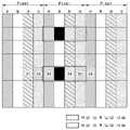
도 1은 본 발명의 실시예에 따른 표시장치의 픽셀을 보여 주는 평면도이다.
도 2a 및 도 2b는 W 암점 픽셀의 보상 전후를 비교한 도면이다.
도 3a 및 도 3b는 W 암점 픽셀의 보상 전후를 비교한 화면 촬영 이미지이다.
도 4a 및 도 4b는 W 암점 픽셀과 그와 이웃한 정상 픽셀의 보상 전후 휘도 변화를 보여 주는 그래프이다.
도 5는 분할 비율 k를 보여 주는 그래프이다.
도 6은 본 발명의 실시예에 따른 OLED 표시장치를 보여 주는 블록도이다.
도 7은 도 6에 도시된 표시장치에서 픽셀의 일 예를 보여 주는 회로도이다.1 is a plan view illustrating a pixel of a display device according to an exemplary embodiment of the present invention.
2A and 2B are diagrams comparing before and after compensation of W dark dot pixels.
3A and 3B are screen shot images comparing before and after compensation of W dark spot pixels.
4A and 4B are graphs illustrating changes in luminance before and after compensation of a W dark dot pixel and a normal pixel adjacent thereto.
5 is a graph showing the split ratio k.
6 is a block diagram illustrating an OLED display device according to an embodiment of the present invention.
7 is a circuit diagram illustrating an example of a pixel in the display device illustrated in FIG. 6 .
이하 첨부된 도면을 참조하여 본 발명에 따른 바람직한 실시예들을 상세히 설명한다. 명세서 전체에 걸쳐서 동일한 참조번호들은 실질적으로 동일한 구성요소들을 의미한다. 이하의 설명에서, 본 발명과 관련된 공지 기능 혹은 구성에 대한 구체적인 설명이 본 발명의 요지를 불필요하게 흐릴 수 있다고 판단되는 경우, 그 상세한 설명을 생략한다.Hereinafter, preferred embodiments according to the present invention will be described in detail with reference to the accompanying drawings. Like reference numerals refer to substantially identical elements throughout. In the following description, if it is determined that a detailed description of a known function or configuration related to the present invention may unnecessarily obscure the gist of the present invention, the detailed description thereof will be omitted.
본 발명의 표시장치는 액정표시장치(Liquid Crystal Display, LCD), OLED 표시장치 등 W 서브 픽셀을 포함하는 WRGB 표시장치로 구현될 수 있다. 이하의 실시예에서, OLED 표시장치를 중심으로 설명되지만, 본 발명은 이에 한정되지 않는다.The display device of the present invention may be implemented as a WRGB display device including W sub-pixels, such as a liquid crystal display (LCD), an OLED display, and the like. In the following embodiments, the OLED display will be mainly described, but the present invention is not limited thereto.
본 발명의 터치 센서는 픽셀 어레이에 내장 가능한 정전 용량 타입의 터치 센서 예를 들면, 상호 용량(mutual capacitance) 센서 또는 자기 용량(Self capacitance) 센서로 구현될 수 있다. 이하에서 터치 센서를 자기 용량 센서 중심으로 설명하지만 본 발명은 이에 한정되지 않는다.The touch sensor of the present invention may be implemented as a capacitive type touch sensor that can be embedded in a pixel array, for example, a mutual capacitance sensor or a self capacitance sensor. Hereinafter, the touch sensor will be described with a focus on the self-capacitance sensor, but the present invention is not limited thereto.
도 1을 참조하면, 본 발명의 WRGB 표시장치는 다수의 픽셀들이 매트릭스 형태로 배치된 표시패널을 포함한다.Referring to FIG. 1 , the WRGB display device of the present invention includes a display panel in which a plurality of pixels are arranged in a matrix form.
픽셀들 각각은 R 서브 픽셀, G 서브 픽셀, B 서브 픽셀 및 W 서브 픽셀로 나뉘어진다. W 서브 픽셀은 RGB 서브 픽셀들 중 이웃한 컬러들 사이에 배치된다. 예를 들어, W 서브 픽셀은 도 1의 예와 같이, R 서브 픽셀과 B 서브 픽셀 사이에 배치될 수 있다. W 서브 픽셀의 배치는 도 1에 한정되지 않는다.Each of the pixels is divided into R sub-pixel, G sub-pixel, B sub-pixel and W sub-pixel. The W sub-pixel is disposed between neighboring colors of the RGB sub-pixels. For example, the W sub-pixel may be disposed between the R sub-pixel and the B sub-pixel, as in the example of FIG. 1 . The arrangement of the W sub-pixels is not limited to FIG. 1 .
W 서브 픽셀이 암점화되거나 수명이 다하여 W 서브 픽셀을 구동할 수 없는 픽셀에서, 암점화된 W 서브 픽셀을 사이에 두고 이격된 R 서브 픽셀과 G 서브 픽셀은 그 물리적 거리가 멀지 않다. 그러나 사용자가 픽셀 어레이와 가까운 거리로 접근하면 암점화된 W 서브 픽셀을 사이에 두고 분리된 R 및 G 서브 픽셀에서 R 파장의 빛과 G 파장의 빛이 섞이지 못하여 1 픽셀 내에서 적색과 녹색이 강하게 인지될 수 있다. 이러한 현상을 컬러 프린징(color fringing)이라 한다. 컬러 프린징 현상으로 인하여, 특정 패턴의 입력 영상이 표시장치에 입력되면, 입력 영상이 표시패널에서 재현될 때 왜곡될 수 있다. 예를 들어, 적색 배경에 백색 라인(white line)이 포함된 이미지를 표시패널에 재현하면 백색 줄이 W 서브 픽셀이 구동되지 않는 픽셀에서 꺾여 보인다.In a pixel in which the W sub-pixel is darkened or the W sub-pixel cannot be driven because the W sub-pixel is darkened, the R sub-pixel and the G sub-pixel spaced apart with the darkened W sub-pixel therebetween are not far apart. However, when the user approaches the pixel array at a close distance, the light of R and G wavelengths cannot be mixed in the R and G subpixels separated by the darkened W subpixel in between, so that red and green are strongly produced within 1 pixel. can be recognized This phenomenon is called color fringing. Due to the color fringing phenomenon, when an input image having a specific pattern is input to the display device, the input image may be distorted when it is reproduced on the display panel. For example, if an image including a white line on a red background is reproduced on the display panel, the white line appears bent at the pixel in which the W sub-pixel is not driven.
이하에서, W 서브 픽셀이 구동되지 않는 픽셀을 “W 암점 픽셀”이라 하고, W 암점 픽셀 주변에 이웃하고 W 서브 픽셀이 정상적으로 구동되는 픽셀을 “정상 픽셀”이라 칭하기로 한다. 도 1의 예에서, W 암점 픽셀은 W 서브 픽셀이 검게 표시되고 박스로 구분된 픽셀이다.Hereinafter, a pixel in which the W sub-pixel is not driven is referred to as a “W dark dot pixel”, and a pixel adjacent to the W dark dot pixel and in which the W sub pixel is normally driven is referred to as a “normal pixel”. In the example of FIG. 1 , the W dark dot pixel is the pixel with the W sub-pixels blacked out and delimited by boxes.
본 발명은 아래에서 자세하게 설명될 휘도 보상 방법을 이용하여 W 암점 픽셀의 휘도를 그와 이웃한 정상 픽셀들의 RGB 서브 픽셀로 분할하여 W 암점 픽셀에서 순색의 인지 휘도(RGB)를 낮추어 컬러 프린징 현상을 감소시킨다. W 암점 픽셀과 정상 픽셀들에서 동일 컬러의 데이터들간에 데이터가 분할된다. 또한, 본 발명은 W 암점 픽셀의 RGB 데이터를 암점화된 W 서브 픽셀의 양측에 이웃한 RGB 서브 픽셀들(31~35)로 분할하여 이웃한 RGB 서브 픽셀들의 백색 휘도를 높임으로써 W 암점 픽셀의 백색 인지 휘도를 상승시킨다.The present invention divides the luminance of the W dark dot pixel into RGB sub-pixels of the adjacent normal pixels using a luminance compensation method to be described in detail below, and lowers the perceived luminance (RGB) of the pure color in the W dark dot pixel, resulting in a color fringing phenomenon. reduces the Data is divided between data of the same color in W dark dot pixel and normal pixels. In addition, the present invention divides the RGB data of the dark-dot W pixel into
본 발명은 소정의 증폭비 만큼 증폭한 W 암점 픽셀의 G 및 B 데이터(Gorg,Borg)와 암점화된 W서브 픽셀의 좌측에 이웃한 제1 정상 픽셀의 G 및 B 데이터(Gsub, Bsub)를 소정의 분할 비율에 따라 서로 나눠 갖는다. 제1 정상 픽셀로 분할 된 G 및 B 데이터는 W 암점 픽셀의 적색 인지 휘도를 낮추어 컬러 프린징 현상을 감소시킨다. 제1 정상 픽셀의 G 및 B 서브 픽셀들(31, 32)과 W 암점 픽셀의 R 서브 픽셀(33)의 빛은 백색광으로 그 서브 픽셀들(31~33)의 백색 인지 휘도가 높아진다. 암점화된 W 서브 픽셀의 좌측에 배치된 RGB 서브 픽셀들(31, 32, 33)에서 녹색 및 청색 광량이 증가하고 그 빛이 W 암점 픽셀의 적색광과 섞여 백색광의 광량이 증가하기 때문에 W 암점 픽셀의 적색 인지 휘도가 낮아지고 백색 인지 휘도가 높아진다.According to the present invention, the G and B data (Gorg, Borg) of the dark dot pixel W amplified by a predetermined amplification ratio and the G and B data (Gsub, Bsub) of the first normal pixel adjacent to the left of the dark dotted W sub-pixel are combined. They are shared with each other according to a predetermined division ratio. The G and B data divided into the first normal pixel lowers the perceived red luminance of the W dark dot pixel, thereby reducing the color fringing phenomenon. Light from the G and B sub-pixels 31 and 32 of the first normal pixel and the
본 발명은 소정의 증폭비 만큼 증폭한 W 암점 픽셀의 R 데이터(Rorg)와 암점화된 W서브 픽셀의 우측에 이웃한 제2 정상 픽셀의 R 데이터(Rsub)를 소정의 분할 비율에 따라 서로 나눠 갖는다. 제2 정상 픽셀로 분할된 R 데이터는 W 암점 픽셀의 녹색 인지 휘도를 낮추어 컬러 프린징 현상을 감소시킨다. 제2 정상 픽셀의 R 서브 픽셀들(36)과 W 암점 픽셀의 G 및 B 서브 픽셀(34, 35)의 빛은 백색광으로 그 서브 픽셀들(34~36)의 백색 인지 휘도가 높아진다. 암점화된 W 서브 픽셀의 우측에 배치된 RGB 서브 픽셀들(34, 35, 36)에서 적색 광량이 증가하고 그 빛이 W 암점 픽셀의 녹색 및 청색광과 섞여 백색광의 광량이 증가하기 때문에 W 암점 픽셀의 녹색 인지 휘도가 낮아지고 백색 인지 휘도가 높아진다.The present invention divides the R data (Rorg) of the dark-dot pixel W amplified by a predetermined amplification ratio and the R data (Rsub) of a second normal pixel adjacent to the right of the dark-dotted W sub-pixel with each other according to a predetermined division ratio. have The R data divided into the second normal pixel lowers the perceived green luminance of the W dark dot pixel, thereby reducing the color fringing phenomenon. Light from the R sub-pixels 36 of the second normal pixel and the G and B sub-pixels 34 and 35 of the W dark dot pixel is white light, and the perceived white luminance of the sub-pixels 34 to 36 is increased. Since the amount of red light increases in the
W 암점 픽셀의 데이터 값을 이웃한 정상 픽셀들로 분할하면 W 암점 픽셀의 휘도가 낮아져 암점으로 보일 수 있다. 이러한 부작용을 방지하기 위하여, 본 발명은 W 암점 픽셀의 데이터 감소로 인한 부작용을 줄이기 위해 증폭비 만큼 W 암점 픽셀의 RGB 데이터를 증폭한다.When the data value of the W dark dot pixel is divided into adjacent normal pixels, the luminance of the W dark dot pixel is lowered, so that it can be seen as a dark dot. In order to prevent such a side effect, the present invention amplifies the RGB data of the W dark dot pixel by the amplification ratio in order to reduce the side effect due to the data reduction of the W dark dot pixel.
본 발명의 휘도 보상 방법은 아래의 수식과 같이 표현될 수 있다.The luminance compensation method of the present invention can be expressed as the following equation.


여기서, Rorg, Gorg 및 Borg는 W 암점 픽셀의 RGB 원 데이터(original data) 값이고, R'org, G'org 및 B'org는 W 암점 서브 픽셀의 데이터 분할 후 RGB 데이터 값이다. Rsub, Gsub 및 Bsub는 W 암점 픽셀과 이웃하는 정상 픽셀들의 RGB 원 데이터(original data) 값이고, R'sub, G'sub 및 B'sub는 W 암점 픽셀과 이웃하는 정상 픽셀들의 데이터 분할 후 RGB 데이터 값이다. k는 W 암점 픽셀의 채도에 따라 가변되는 분할 비율이다. 1ⅹ2kp는 W 암점 픽셀 데이터의 증폭비율이다.Here, Rorg, Gorg, and Borg are the RGB original data values of the W dark dot pixel, and R'org, G'org and B'org are the RGB data values of the W dark dot subpixel after data division. Rsub, Gsub and Bsub are RGB original data values of the W dark dot pixel and neighboring normal pixels, and R'sub, G'sub and B'sub are RGB after data division of the W dark dot pixel and neighboring normal pixels. data value. k is a division ratio that varies according to the saturation of the W dark dot pixel. 1×2kp is the amplification ratio of W dark dot pixel data.
k는 W 암점 픽셀의 채도가 높으면 0(zero)에 가까워지고, 채도가 낮을수록 즉, 무채색에 가까울수록 최대값에 가까워진다. W 암점 픽셀이 순색(RGBCMY)이거나 유채색이면 이웃 픽셀로 W 암점 픽셀의 휘도가 이웃 픽셀로 거의 분할되지 않는다. 반면에, 암점 픽셀이 무채색에 가까울수록 W 암점 픽셀의 휘도가 이웃 픽셀로 많이 분할된다. W 암점 픽셀의 데이터가 유채색 데이터일 때 W 암점 픽셀의 데이터를 제1 및 제2 정상 픽셀로 과도하게 분할하면 컬러 왜곡으로 인하여 사용자가 색감 저하를 인지할 수 있다.k approaches 0 (zero) when the saturation of the W dark dot pixel is high, and approaches the maximum value as the saturation is low, that is, as it approaches an achromatic color. If the W dark dot pixel is a pure color (RGBCMY) or a chromatic color, the luminance of the W dark dot pixel is hardly divided into neighboring pixels. On the other hand, as the dark dot pixel is closer to an achromatic color, the luminance of the W dark dot pixel is more divided into neighboring pixels. When the data of the W dark dot pixel is chromatic color data, if the data of the W dark dot pixel is excessively divided into the first and second normal pixels, the user may perceive color degradation due to color distortion.
k가 높으면 제1 및 제2 정상 픽셀에 더해지는 데이터값이 커져 그 정상 픽셀들이 휘점으로 보일 수 있다. 실험 결과에 따르면, k가 0.5 보다 크면 정상 픽셀의 휘도가 과도하게 상승하여 휘점으로 보일 수 있다. 따라서, 본 발명은 분담 비율 k를 0 ~ 0.5로 제한한다.When k is high, the data value added to the first and second normal pixels increases, so that the normal pixels can be seen as bright points. According to the experimental results, when k is greater than 0.5, the luminance of the normal pixel is excessively increased, and thus it may appear as a bright point. Accordingly, the present invention limits the contribution ratio k to 0 to 0.5.
p는 0(zero) 보다 큰 값으로 설정된 휘도 증가 비율이다. p는 0 보다 크고 1 이하의 값으로 설정되어 W 암점 픽셀의 데이터 분할로 인하여 W 암점 픽셀의 휘도가 저하되는 현상을 한다. 이웃한 픽셀들 간 데이터 분할로 인하여 자신의 휘도가 과도하게 저하되는 것을 방지하기 위하여 설정된다.p is a luminance increase ratio set to a value greater than 0 (zero). p is greater than 0 and set to a value less than or equal to 1, so that the luminance of the W dark dot pixel is lowered due to data division of the W dark dot pixel. It is set to prevent excessive degradation of its own luminance due to data division between neighboring pixels.
도 2a 및 도 2b는 W 암점 픽셀의 보상 전후를 비교한 도면이다. 도 3a 및 도 3b는 W 암점 픽셀의 보상 전후를 비교한 화면 촬영 이미지이다. 도 4a 및 도 4b는 W 암점 픽셀과 그와 이웃한 정상 픽셀의 보상 전후 휘도 변화를 보여 주는 그래프이다. 도 4a 및 도 4b에서 B 서브 픽셀의 인지 휘도는 생략되어 있다. 도 2a 내지 도 4b는 W 암점 픽셀에서 RGB 서브 픽셀이 고계조의 휘도로 발광된 예이고, 정상 픽셀들에서 W 서브 픽셀만 발광하고 RGB 서브 픽셀들의 휘도가 저계조인 예이다.2A and 2B are diagrams comparing before and after compensation of W dark dot pixels. 3A and 3B are screen shot images comparing before and after compensation of W dark spot pixels. 4A and 4B are graphs illustrating changes in luminance before and after compensation of a W dark dot pixel and a normal pixel adjacent thereto. The perceived luminance of sub-pixel B is omitted in FIGS. 4A and 4B . 2A to 4B are examples in which the RGB sub-pixels emit light with high grayscale luminance in the W dark dot pixel, and only the W sub-pixels emit light in normal pixels and the RGB sub-pixels emit light with low grayscale luminance.
W 암점 픽셀은 W 서브 픽셀이 구동되지 않기 때문에 도 2a 및 도 3a와 같이 W 서브 픽셀을 사이에 두고 분리된 RGB 파장의 빛이 백생광으로 섞이지 않고 개별 컬러로 보일 수 있다. 이는 도 4a의 인지 휘도에서 알 수 있다. 도 4a에서 알 수 있는 바와 같이, 보상전 W 암점 픽셀에서 W 암점 서브 픽셀에서 백색 인지 휘도가 낮고 순색(RGBCMY) 휘도가 더 높아져 컬러 프린징 현상이 나타난다. 반면에, 본 발명은 도 4b에서 명백히 알 수 있는 바와 같이 W 암점 픽셀의 RGB 데이터값을 증폭하여 이웃한 정상 서브 픽셀들로 분할함으로써 W 암점 픽셀의 순색(RGBCMY) 휘도를 낮춤과 동시에 암점화된 W 서브 픽셀과 이웃하는 RGB 서브 픽셀(31~36)의 백색 휘도를 높여 W 암점 픽셀의 W 인지 휘도를 높인다.Since the W sub-pixel is not driven in the W dark dot pixel, as shown in FIGS. 2A and 3A , the RGB wavelength light separated with the W sub-pixel therebetween is not mixed into white light and can be viewed as individual colors. This can be seen from the perceived luminance of FIG. 4A. As can be seen from FIG. 4A , in the W dark dot pixel before compensation, the white perceived luminance is low in the W dark dot sub-pixel and the RGBCMY luminance is higher, resulting in a color fringing phenomenon. On the other hand, in the present invention, as can be clearly seen from FIG. 4B , the RGB data value of the W dark dot pixel is amplified and divided into adjacent normal sub-pixels, thereby lowering the RGBCMY luminance of the W dark dot pixel and simultaneously darkening the dark dot pixel. By increasing the white luminance of the RGB sub-pixels 31 to 36 adjacent to the W sub-pixel, the W perceived luminance of the W dark dot pixel is increased.
도 6은 본 발명의 실시예에 따른 OLED 표시장치를 보여 주는 블록도이다. 도 7은 도 6에 도시된 픽셀의 일 예를 보여 주는 등가 회로도이다.6 is a block diagram illustrating an OLED display device according to an embodiment of the present invention. 7 is an equivalent circuit diagram illustrating an example of the pixel illustrated in FIG. 6 .
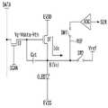
도 6 및 도 7을 참조하면, 본 발명의 실시예에 따른 OLED 표시장치는 표시패널(10)과, 그 표시패널(10)에 데이터를 기입하기 위한 구동 회로를 포함한다.6 and 7 , an OLED display device according to an exemplary embodiment of the present invention includes a
표시패널(10)에는 다수의 데이터 라인들(14)과 다수의 게이트 라인들(15)이 교차되고, 픽셀들이 매트릭스 형태로 배치된다. 표시패널(10)의 픽셀 어레이(Pixel array)에 입력 영상의 데이터가 표시된다. 표시패널(10)은 기준 전압 라인(이하, “REF 라인”이라 함)(REF), 고전위 구동 전압(EVDD)을 픽셀들에 공급하는 EVDD 라인을 포함한다. REF 라인은 기준 전압원으로부터의 기준 전압(Vref)을 픽셀들에 공급한다. 센싱 기간 동안 픽셀의 구동 특성 변화는 REF 라인(REF)를 통해 센싱되고, 정상 구동(Normal drive) 기간 동안 REF 라인(REF)을 통해 픽셀들에 소정의 기준 전압(Vref)이 공급된다. 기준 전압(Vref)은 0 보다 큰 전압 예를 들어, 2V로 설정될 수 있으나 이에 한정되지 않는다. 기준 전압(Vref)은 표시장치의 해상도, 구동 방법 등에 따라 달라질 수 있다.In the
픽셀들 각각은 컬러 구현을 위하여 R 서브 픽셀, G 서브 픽셀, B 서브 픽셀 및 W 백색 서브 픽셀로 나뉘어진다. 이하의 설명에서, 픽셀은 서브 픽셀을 의미한다. 픽셀들 각각에 하나의 데이터 라인, 하나의 REF 라인, 하나의 EVDD 라인 등의 배선이 연결된다.Each of the pixels is divided into an R sub-pixel, a G sub-pixel, a B sub-pixel and a W white sub-pixel for color implementation. In the following description, a pixel means a sub-pixel. A wiring such as one data line, one REF line, and one EVDD line is connected to each of the pixels.
구동 회로는 데이터 구동부(12), 게이트 구동부(13), 및 타이밍 콘트롤러(11)를 포함한다.The driving circuit includes a
데이터 구동부(12)는 미리 설정된 센싱 기간 동안 타이밍 콘트롤러(11)의 제어 하에 센싱용 데이터 전압을 픽셀들에 공급한다. 센싱 기간은 프레임 기간들 사이에서 입력 영상의 데이터가 수신되지 않는 블랭크 기간 즉, 버티컬 블랭크 기간(Vertical Blank Period)으로 할당될 수 있다. 센싱 기간은 표시장치의 전원이 켜진 직후 또는 표시장치의 전원이 꺼진 직후의 소정 기간을 포함할 수 있다. 센싱용 데이터 전압은 센싱 기간 동안 픽셀들의 구동 TFT의 게이트에 인가된다. 센싱용 데이터 전압은 센싱 기간 동안 구동 TFT를 턴-온(turn-on)시켜 그 구동 TFT에서 전류가 흐르게 한다. 센싱용 데이터 전압(SDATA)은 미리 설정된 계조에 대응하는 전압으로 발생된다. 센싱용 데이터 전압(SDATA)은 센싱 계조에 따라 가변될 수 있다.The
타이밍 콘트롤러(11)는 센싱 기간 동안 내장 메모리에 미리 저장된 센싱용 데이터를 데이터 구동부(12)로 전송한다. 센싱용 데이터는 입력 영상의 데이터와는 무관하게 미리 설정되어 픽셀의 구동 특성을 센싱하기 위한 데이터이다. 데이터 구동부(12)는 디지털 데이터로 수신된 센싱용 데이터를 디지털 아날로그 컨버터(Digital to Analog Converter, 이하 "DAC"라 함)를 통해 감마 보상 전압으로 변환하여 센싱용 데이터 전압을 출력한다.The
센싱 경로는 센싱용 데이터 전압이 픽셀에 공급될 때 그 픽셀의 전류로 발생하는 전압을 디지털 데이터로 변환하여 센싱값(SEN)을 발생한다. 센싱 경로는 REF 라인(REF), 센싱 전압을 디지털 데이터로 변환하는 아날로그 디지털 컨버터(Analog Digital Converter, 이하 “ADC”라 함), 도시하지 않은 샘플 & 홀더(Sample & Holder)를 포함한다. 센싱 경로에는 제1 및 제2 스위치 소자(SW1, SW2)가 연결될 수 있다. 제1 스위치 소자(SW1)는 센싱 기간 동안 턴-온(turn-on)되어 ADC를 픽셀에 연결하고, 정상 구동 기간 동안 턴-오프(turn-off)되어 ADC와 픽셀 사이의 전류 패스를 차단할 수 있다. 반면에, 제2 스위치 소자(SW2)는 센싱 기간 동안 턴-오프되고, 정상 구동 기간 동안 턴-온되어 기준 전압(Vref)을 픽셀에 공급할 수 있다. 샘플 & 홀더는 제1 스위치 소자(SW1)와 REF 라인(REF)에 연결된 커패시터(Capacitor)로 구성될 수 있다. 샘플 & 홀더는 커패시터에 센싱 전압을 저장함으로써 센싱 전압을 샘플링하여 ADC로 공급한다. 데이터 구동부(12)는 픽셀의 센싱값을 타이밍 콘트롤러(11)로 전송한다.The sensing path generates a sensing value SEN by converting a voltage generated by a current of the pixel into digital data when a sensing data voltage is supplied to the pixel. The sensing path includes a REF line (REF), an analog-to-digital converter (hereinafter referred to as “ADC”) that converts the sensing voltage into digital data, and a sample & holder (not shown). The first and second switch elements SW1 and SW2 may be connected to the sensing path. The first switch element SW1 is turned on during the sensing period to connect the ADC to the pixel, and is turned off during the normal driving period to block the current path between the ADC and the pixel. have. On the other hand, the second switch element SW2 may be turned off during the sensing period and turned on during the normal driving period to supply the reference voltage Vref to the pixel. The sample & holder may include the first switch element SW1 and a capacitor connected to the REF line REF. The sample & holder stores the sensed voltage in a capacitor, samples the sensed voltage and supplies it to the ADC. The
데이터 구동부(12)는 입력 영상을 표시하는 정상 구동 기간 동안 DAC를 통해 타이밍 콘트롤러(11)로부터 수신되는 입력 영상의 디지털 비디오 데이터(MDATA)를 감마 보상 전압으로 변환하여 데이터 전압을 발생한다. 데이터 전압은 데이터 라인들(14)을 통해 픽셀들에 공급된다. 데이터 구동부(12)에 공급되는 디지털 비디오 데이터(MDATA)는 타이밍 콘트롤러(11)에 의해 변조된 데이터(MDATA)이다. 정상 구동 기간 동안, REF 라인(REF)을 통해 픽셀들에는 소정의 기준 전압이 공급된다. 센싱 경로에 연결된 회로 소자들은 데이터 구동부(12)와 함께 IC(Integrated Circuit) 칩에 집적될 수 있다.The
데이터 구동부(12)로부터 출력되는 데이터 전압의 전압 범위는 후술하는 바와 같이 보상 전압 마진 만큼 확대된다. 보상 전압 마진은 구동 TFT의 소스에 인가되는 전압 예를 들어 기준 전압(Vref) 만큼 확보될 수 있다.The voltage range of the data voltage output from the
게이트 구동부(13)는 스캔 펄스(SCAN)를 발생하여 게이트 라인들(15)에 공급한다. 스캔 펄스(SCAN)는 도 2에 도시된 스위치 TFT(ST)에 공급된다. 게이트 구동부(13)는 시프트 레지스터(Shift register)를 이용하여 스캔 펄스를 시프트시킴으로써 그 스캔 펄스(SCAN)를 게이트 라인들(15)에 순차적으로 공급할 수 있다. 게이트 구동부(13)의 시프트 레지스터는 GIP(Gate-driver In Panel) 공정으로 픽셀 어레이와 함께 표시패널(10)의 기판 상에 직접 형성될 수 있다.The
타이밍 콘트롤러(11)는 도시하지 않은 호스트 시스템으로부터 입력 영상의 디지털 비디오 데이터(DATA)와, 그와 동기되는 타이밍 신호를 수신한다. 타이밍 신호는 수직 동기신호(Vsync), 수평 동기신호(Hsync), 클럭 신호(DCLK) 및 데이터 인에이블신호(DE) 등을 포함한다. 호스트 시스템은 TV(Television) 시스템, 셋톱박스, 네비게이션 시스템, DVD 플레이어, 블루레이 플레이어, 개인용 컴퓨터(PC), 홈 시어터 시스템, 폰 시스템(Phone system) 중 어느 하나일 수 있다.The
타이밍 콘트롤러(11)는 호스트 시스템으로부터 수신된 타이밍 신호를 바탕으로서 데이터 구동부(12)의 동작 타이밍을 제어하기 위한 데이터 타이밍 제어 신호(DDC)와, 게이트 구동부(13)의 동작 타이밍을 제어하기 위한 게이트 타이밍 제어 신호(GDC), 제1 및 제2 스위치 소자들(SW1, SW2)의 동작 타이밍을 제어하기 위한 스위치 제어 신호 등을 발생할 수 있다.The
타이밍 콘트롤러(11)는 RGBW 데이터 생성부(21), 휘도 보상부(22), 및 구동 특성 보상부(23)를 포함한다. RGBW 데이터 생성부(21)는 공지된 화이트 게인 산출 알고리즘을 이용하여 입력 영상의 RGB 데이터를 RGBW 데이터로 변환한다.The
휘도 보상부(22)는 도 1 내지 도 5를 결부하여 전술한 휘도 보상 방법으로 W 암점 픽셀의 휘도를 보상한다. W 암점 픽셀은 제조 공정에서 발견되어 타이밍 콘트롤러에 그 위치 정보가 미리 저장될 수 있다. 또한, W 암점 픽셀은 센싱 경로를 통해 얻어진 센싱값을 통해 수명이 다할 때 감지될 수 있다.The
구동 특성 보상부(23)는 센싱값(SEN)을 바탕으로 픽셀들 각각의 구도 특성 변화를 판단하여 센싱값(SEN)에 따른 보상값으로 픽셀들에 기입될 데이터를 변조한다. 구동 특성 보상부(23)는 픽셀들로부터 수신된 센싱값(SEN)을 바탕으로 픽셀들 각각에서 구동 특성 변화를 보상하기 위한 보상값을 선택한다. 보상값은 픽셀의 구동 특성 변화를 고려하여 미리 설정되어 룩업 테이블(Look-up table, LUT)의 메모리에 저장될 수 있다. 보상값은 공지된 외부 보상 방법에서 제안된 보상 방법으로 적용될 수 있으므로 이에 대한 상세한 설명을 생략한다. 구동 특성 보상부(23)는 보상값으로 픽셀에 기입될 입력 영상의 데이터를 변조한다. 보상값은 구동 TFT의 문턱 전압 변화를 보상하기 위한 옵셋값(Offset)과, 구동 TFT의 이동도 변화를 보상하기 위한 게인값(gain)을 포함한다. 옵셋값은 픽셀들에 기입될 데이터에 더해져 구동 TFT(DT)의 문턱 전압 변화를 보상한다. 게인값은 픽셀들에 기입될 데이터에 곱해져 구동 TFT(DT)의 이동도 변화를 보상한다.The driving
픽셀들 각각은 OLED, 구동 TFT(DT), 스위치 TFT(ST), 스토리지 커패시터(Cst) 등을 포함한다. 픽셀 회로는 도 7에 한정되지 않는다는 것에 주의하여야 한다.Each of the pixels includes an OLED, a driving TFT (DT), a switch TFT (ST), a storage capacitor (Cst), and the like. It should be noted that the pixel circuit is not limited to FIG. 7 .
OLED는 애노드와 캐소드 사이에 형성된 유기 화합물층을 포함한다. 유기 화합물층은 정공주입층(HIL), 정공수송층(HTL), 발광층(EML), 전자수송층(ETL), 전자주입층(EIL) 등을 포함할 수 있으나, 이에 한정되지 않는다.The OLED includes an organic compound layer formed between an anode and a cathode. The organic compound layer may include, but is not limited to, a hole injection layer (HIL), a hole transport layer (HTL), an emission layer (EML), an electron transport layer (ETL), an electron injection layer (EIL), and the like.
TFT들(ST, DT)은 도 7에서 n 타입 MOSFET로 예시되었으나 p 타입 MOSFET(Metal-Oxide Semiconductor Field Effect Transistor)로 구현될 수 있다. TFT들은 비정질 실리콘(a-Si) TFT, 폴리 실리콘 TFT, 산화물 반도체 TFT 중 어느 하나 또는 그 조합으로 구현될 수 있다.Although the TFTs ST and DT are illustrated as n-type MOSFETs in FIG. 7 , they may be implemented as p-type MOSFETs (Metal-Oxide Semiconductor Field Effect Transistors). The TFTs may be implemented by any one or a combination of an amorphous silicon (a-Si) TFT, a polysilicon TFT, and an oxide semiconductor TFT.
OLED의 애노드는 제2 노드(B)를 경유하여 구동 TFT(DT)에 연결된다. OLED의 캐소드는 기저 전압원에 연결되어 기저 전압(EVSS)이 공급된다.The anode of the OLED is connected to the driving TFT (DT) via the second node (B). The cathode of the OLED is connected to a base voltage source to supply a base voltage (EVSS).
구동 TFT(DT)는 게이트-소스 간 전압(Vgs)에 따라 OLED에 흐르는 전류를 조절한다. 구동 TFT(DT)는 제1 노드(A)에 접속된 게이트, 고전위 구동 전압(EVDD)이 공급되는 드레인, 및 제2 노드(B)에 접속된 소스를 포함한다. 스토리지 커패시터(C)는 제1 노드(A)와 제2 노드(B) 사이에 접속되어 구동 TFT(DT)의 게이트-소스간 전압(Vgs)을 유지한다.The driving TFT DT controls the current flowing through the OLED according to the gate-source voltage Vgs. The driving TFT DT includes a gate connected to the first node A, a drain to which the high potential driving voltage EVDD is supplied, and a source connected to the second node B. The storage capacitor C is connected between the first node A and the second node B to maintain the gate-source voltage Vgs of the driving TFT DT.
스위치 TFT(ST)는 스캔 펄스(SCAN)에 응답하여 데이터 라인(14)으로부터의 데이터 전압(Vdata)을 제1 노드(A)에 공급한다. 스위치 TFT(ST)는 스캔 펄스(SCAN)가 공급되는 게이트, 데이터 라인(14)에 접속된 드레인, 및 제1 노드(A)에 접속된 소스를 포함한다.The switch TFT ST supplies the data voltage Vdata from the
구동 TFT(DT)의 문턱 전압을 외부 보상 방법으로 보상할 수 있다. 외부 보상 방법은 구동 TFT(DT)를 소스 팔로워(Source Follower)로 동작시켜서 구동 TFT(DT)의 문턱전압(Vth)을 센싱한다. 이 방법은 ADC에 입력되는 센싱 전압을 바탕으로 구동 TFT(DT)의 문턱 전압(Vth)을 판단한다. 구동 TFT(DT)의 문턱 전압(Vth)을 센싱하기 위하여, 구동 TFT(DT)의 게이트에 문턱 전압(Vth)보다 큰 데이터전압(Vdata)이 인가되고, 구동 TFT(DT)의 소스에 기준 전압(Vref)이 인가된다. 구동 TFT(DT)의 게이트-소스 간 전압(Vgs)는 문턱 전압(Vth)보다 클 때 구동 TFT(DT)가 턴-온 된다. 이 때, 구동 TFT(DT)의 드레인-소스 간 전류(Ids)는 구동 TFT(DT)의 게이트-소스간 전압(Vgs)에 의존한다. 구동 TFT(DT)의 드레인-소스 간 전류(Ids)는 고전위 구동 전압(EVDD)으로 인하여 상승하여 구동 TFT(DT)의 소스 전압(Vs)을 높인다. 구동 TFT(DT)의 소스 전압(Vs)이 증가하기 시작하는 센싱 초기(Tx)에 구동 TFT(DT)의 게이트-소스간 전압(Vgs)이 크므로 구동 TFT(DT)의 채널 저항이 작고 그 결과 구동 TFT(DT)의 드레인-소스 간 전류(Ids)는 상승한다. 구동 TFT(DT)의 소스 전압(Vs)이 상승할수록 구동 TFT(DT)의 게이트-소스 간 전압(Vgs)은 작아지므로 구동 TFT(DT)의 채널 저항이 커지고, 그 결과 구동 TFT(DT)의 드레인-소스 간 전류(Ids)는 감소된다. 구동 TFT(DT)의 소스 전압(Vgs)이 포화될 때 게이트-소스 간 전압(Vgs)이 문턱 전압(Vth)이다.The threshold voltage of the driving TFT DT may be compensated by an external compensation method. The external compensation method senses the threshold voltage Vth of the driving TFT DT by operating the driving TFT DT as a source follower. In this method, the threshold voltage (Vth) of the driving TFT (DT) is determined based on the sensing voltage input to the ADC. In order to sense the threshold voltage Vth of the driving TFT DT, a data voltage Vdata greater than the threshold voltage Vth is applied to the gate of the driving TFT DT, and a reference voltage is applied to the source of the driving TFT DT. (Vref) is applied. When the gate-source voltage Vgs of the driving TFT DT is greater than the threshold voltage Vth, the driving TFT DT is turned on. At this time, the drain-source current Ids of the driving TFT DT depends on the gate-source voltage Vgs of the driving TFT DT. The drain-source current Ids of the driving TFT DT rises due to the high potential driving voltage EVDD to increase the source voltage Vs of the driving TFT DT. Since the gate-source voltage (Vgs) of the driving TFT (DT) is large in the initial sensing period (Tx) when the source voltage (Vs) of the driving TFT (DT) starts to increase, the channel resistance of the driving TFT (DT) is small and its As a result, the drain-source current Ids of the driving TFT DT rises. As the source voltage Vs of the driving TFT DT increases, the gate-source voltage Vgs of the driving TFT DT decreases, so that the channel resistance of the driving TFT DT increases. As a result, the channel resistance of the driving TFT DT increases. The drain-source current Ids is reduced. When the source voltage Vgs of the driving TFT DT is saturated, the gate-source voltage Vgs is the threshold voltage Vth.
이상 설명한 내용을 통해 당업자라면 본 발명의 기술사상을 일탈하지 아니하는 범위에서 다양한 변경 및 수정이 가능함을 알 수 있을 것이다. 따라서, 본 발명의 기술적 범위는 명세서의 상세한 설명에 기재된 내용으로 한정되는 것이 아니라 특허 청구의 범위에 의해 정하여져야만 할 것이다.Those skilled in the art from the above description will be able to see that various changes and modifications can be made without departing from the technical spirit of the present invention. Accordingly, the technical scope of the present invention should not be limited to the contents described in the detailed description of the specification, but should be defined by the claims.
10 : 표시패널11 : 타이밍 콘트롤러
12 : 데이터 구동부13 : 게이트 구동부
14 : 데이터 라인15 : 게이트 라인
21 : RGBW 데이터 생성부22 : 휘도 보상부
23 : 구동 특성 보상부10: display panel 11: timing controller
12: data driver 13: gate driver
14: data line 15: gate line
21: RGBW data generation unit 22: luminance compensator
23: driving characteristic compensator
Claims (12)
Translated fromKorean상기 픽셀들에 데이터를 기입하는 구동 회로;
상기 백색 서브 픽셀이 구동 불능 상태인 W 암점 픽셀의 적색, 녹색 및 청색 데이터를 상기 W 암점 픽셀과 이웃하는 제1 및 제2 정상 픽셀들로 분할하는 휘도 보상부를 포함하고,
상기 제1 정상 픽셀은 상기 W 암점 픽셀의 일측과 이웃하고, 상기 제2 정상 픽셀은 상기 W 암점 픽셀의 타측과 이웃하는 표시장치.a display panel comprising a plurality of pixels, each of which is divided into a red sub-pixel, a green sub-pixel, a blue sub-pixel, and a white sub-pixel;
a driving circuit for writing data to the pixels;
and a luminance compensator for dividing red, green, and blue data of the dark W pixel in which the white sub-pixel is in a non-drivable state into first and second normal pixels adjacent to the W dark pixel;
The first normal pixel is adjacent to one side of the W dark dot pixel, and the second normal pixel is adjacent to the other side of the W dark dot pixel.
상기 W 암점 픽셀의 데이터는 증폭되어 동일 컬러별로 상기 제1 및 제2 정상 픽셀들의 데이터로 분할되는 표시장치.The method of claim 1,
The data of the W dark dot pixel is amplified and divided into data of the first and second normal pixels according to the same color.
상기 W 암점 픽셀과 상기 제1 정상 픽셀이 상기 녹색 및 청색 데이터를 소정의 분할 비율로 서로 나눠 가지며,
상기 W 암점 픽셀과 상기 제2 정상 픽셀이 상기 적색 데이터를 소정의 분할 비율로 서로 나눠 갖는 표시장치.3. The method of claim 2,
the W dark dot pixel and the first normal pixel divide the green and blue data by a predetermined division ratio;
A display device in which the W dark dot pixel and the second normal pixel divide the red data by a predetermined division ratio.
상기 W 암점 픽셀의 데이터 분할 결과, 상기 W 암점 픽셀의 적색, 녹색 및 청색 인지 휘도가 낮아지는 표시장치.4. The method of claim 3,
A display device in which perceived luminance of red, green, and blue of the W dark dot pixel is lowered as a result of data division of the W dark dot pixel.
상기 W 암점 픽셀의 데이터 분할 결과, 상기 W 암점 픽셀의 백색 휘도가 상승하는 표시장치.5. The method of claim 4,
As a result of data division of the W dark dot pixel, the white luminance of the W dark dot pixel increases.
상기 휘도 보상부는 아래의 수식을 바탕으로 상기 W 암점 픽셀의 데이터를 상기 제1 및 제2 정상 픽셀들로 분할하는 표시장치.


여기서, Rorg, Gorg 및 Borg는 상기 W 암점 픽셀의 RGB 원 데이터 값, R'org, G'org 및 B'org는 상기 W 암점 서브 픽셀의 데이터 분할 후 RGB 데이터 값이다. Rsub, Gsub 및 Bsub는 W 암점 픽셀과 이웃하는 정상 픽셀들의 RGB 원 데이터(original data) 값이고, R'sub, G'sub 및 B'sub는 W 암점 픽셀과 이웃하는 정상 픽셀들의 데이터 분할 후 RGB 데이터 값이다. k는 상기 W 암점 픽셀의 채도에 따라 가변되는 분할 비율로서 0~0.5 사이의 값이다. p는 0(zero) 보다 큰 값으로 설정된 휘도 증가 비율로서 0 보다 크고 1 이하의 값이다.4. The method of claim 3,
The luminance compensator divides the data of the W dark dot pixel into the first and second normal pixels based on the following equation.
Here, Rorg, Gorg, and Borg are the RGB raw data values of the W dark dot pixel, and R'org, G'org and B'org are the RGB data values of the W dark dot subpixel after data division. Rsub, Gsub and Bsub are the RGB original data values of the W dark dot pixel and neighboring normal pixels, and R'sub, G'sub and B'sub are RGB after data division of the W dark dot pixel and the neighboring normal pixels. data value. k is a division ratio varying according to the saturation of the W dark dot pixel, and is a value between 0 and 0.5. p is a luminance increase ratio set to a value greater than 0 (zero), and is greater than 0 and less than or equal to 1.
상기 k가 W 암점 픽셀에 기입될 데이터의 채도가 높을수록 낮아지고, 채도가 낮을수록 커지는 표시장치.7. The method of claim 6,
A display device in which k decreases as the saturation of data to be written into the W dark dot pixel increases, and increases as the saturation decreases.
상기 백색 서브 픽셀이 구동 불능 상태인 W 암점 픽셀의 적색, 녹색 및 청색 데이터를 상기 W 암점 픽셀과 이웃하는 제1 및 제2 정상 픽셀들로 분할하는 단계를 포함하고,
상기 제1 정상 픽셀은 상기 W 암점 픽셀의 일측과 이웃하고, 상기 제2 정상 픽셀은 상기 W 암점 픽셀의 타측과 이웃하는 표시장치의 구동 방법.A method of driving a display device having a display panel including a plurality of pixels, each of which is divided into a red sub-pixel, a green sub-pixel, a blue sub-pixel and a white sub-pixel, the method comprising:
dividing the red, green, and blue data of the dark W pixel in which the white sub-pixel is in a non-drivable state into first and second normal pixels adjacent to the W dark pixel;
The first normal pixel is adjacent to one side of the W dark dot pixel, and the second normal pixel is adjacent to the other side of the W dark dot pixel.
상기 백색 서브 픽셀이 구동 불능 상태인 W 암점 픽셀의 적색, 녹색 및 청색 데이터를 상기 W 암점 픽셀과 이웃하는 제1 및 제2 정상 픽셀들로 분할하는 단계는,
상기 W 암점 픽셀의 데이터를 증폭하여 동일 컬러별로 상기 제1 및 제2 정상 픽셀들의 데이터로 분할하는 단계를 포함하는 표시장치의 구동 방법.9. The method of claim 8,
dividing the red, green, and blue data of the dark W pixel in which the white sub-pixel is in a non-driving state into first and second normal pixels adjacent to the W dark pixel;
and amplifying the data of the W dark dot pixel and dividing the data into the data of the first and second normal pixels according to the same color.
상기 W 암점 픽셀과 상기 제1 정상 픽셀이 상기 녹색 및 청색 데이터를 소정의 분할 비율로 서로 나눠 가지며,
상기 W 암점 픽셀과 상기 제2 정상 픽셀이 상기 적색 데이터를 소정의 분할 비율로 서로 나눠 갖는 표시장치의 구동 방법.10. The method of claim 9,
the W dark dot pixel and the first normal pixel divide the green and blue data by a predetermined division ratio;
A method of driving a display device in which the W dark dot pixel and the second normal pixel divide the red data by a predetermined division ratio.
상기 분할하는 단계는 아래의 수식을 바탕으로 상기 W 암점 픽셀의 데이터를 상기 제1 및 제2 정상 픽셀들로 분할하는 표시장치의 구동 방법.


여기서, Rorg, Gorg 및 Borg는 상기 W 암점 픽셀의 RGB 원 데이터 값, R'org, G'org 및 B'org는 상기 W 암점 서브 픽셀의 데이터 분할 후 RGB 데이터 값이다. Rsub, Gsub 및 Bsub는 W 암점 픽셀과 이웃하는 정상 픽셀들의 RGB 원 데이터(original data) 값이고, R'sub, G'sub 및 B'sub는 W 암점 픽셀과 이웃하는 정상 픽셀들의 데이터 분할 후 RGB 데이터 값이다. k는 상기 W 암점 픽셀의 채도에 따라 가변되는 분할 비율로서 0~0.5 사이의 값이다. p는 0(zero) 보다 큰 값으로 설정된 휘도 증가 비율로서 0 보다 크고 1 이하의 값이다.11. The method of claim 10,
The dividing may include dividing the data of the W dark dot pixel into the first and second normal pixels based on the following equation.
Here, Rorg, Gorg, and Borg are the RGB raw data values of the W dark dot pixel, and R'org, G'org and B'org are the RGB data values of the W dark dot subpixel after data division. Rsub, Gsub and Bsub are the RGB original data values of the W dark dot pixel and neighboring normal pixels, and R'sub, G'sub and B'sub are RGB after data division of the W dark dot pixel and the neighboring normal pixels. data value. k is a division ratio varying according to the saturation of the W dark dot pixel, and is a value between 0 and 0.5. p is a luminance increase ratio set to a value greater than 0 (zero), and is greater than 0 and less than or equal to 1.
상기 k가 W 암점 픽셀에 기입될 데이터의 채도가 높을수록 낮아지고, 채도가 낮을수록 커지는 표시장치의 구동 방법.12. The method of claim 11,
The method of driving a display device, wherein k decreases as the saturation of data to be written into the W dark dot pixel increases, and increases as the saturation decreases.
Priority Applications (1)
| Application Number | Priority Date | Filing Date | Title |
|---|---|---|---|
| KR1020150150500AKR102456428B1 (en) | 2015-10-28 | 2015-10-28 | Display Device having white sub-pixel and Method of Driving the same |
Applications Claiming Priority (1)
| Application Number | Priority Date | Filing Date | Title |
|---|---|---|---|
| KR1020150150500AKR102456428B1 (en) | 2015-10-28 | 2015-10-28 | Display Device having white sub-pixel and Method of Driving the same |
Publications (2)
| Publication Number | Publication Date |
|---|---|
| KR20170049788A KR20170049788A (en) | 2017-05-11 |
| KR102456428B1true KR102456428B1 (en) | 2022-10-20 |
Family
ID=58742213
Family Applications (1)
| Application Number | Title | Priority Date | Filing Date |
|---|---|---|---|
| KR1020150150500AActiveKR102456428B1 (en) | 2015-10-28 | 2015-10-28 | Display Device having white sub-pixel and Method of Driving the same |
Country Status (1)
| Country | Link |
|---|---|
| KR (1) | KR102456428B1 (en) |
Families Citing this family (3)
| Publication number | Priority date | Publication date | Assignee | Title |
|---|---|---|---|---|
| KR102599509B1 (en)* | 2018-12-20 | 2023-11-08 | 엘지디스플레이 주식회사 | Electroluminescence display and methode of driving the same |
| KR102821852B1 (en) | 2020-08-27 | 2025-06-17 | 엘지디스플레이 주식회사 | Display panel and display device including the same |
| CN114187862B (en)* | 2021-12-15 | 2024-02-23 | 厦门天马微电子有限公司 | Display device and display device driving method |
Citations (1)
| Publication number | Priority date | Publication date | Assignee | Title |
|---|---|---|---|---|
| JP2013120321A (en) | 2011-12-08 | 2013-06-17 | Sony Corp | Display unit and electronic apparatus |
Family Cites Families (4)
| Publication number | Priority date | Publication date | Assignee | Title |
|---|---|---|---|---|
| KR101782054B1 (en)* | 2011-02-14 | 2017-09-26 | 엘지디스플레이 주식회사 | Liquid crystal display device and driving method thereof |
| KR102090706B1 (en)* | 2012-12-28 | 2020-03-19 | 삼성디스플레이 주식회사 | Display device, Optical compensation system and Optical compensation method thereof |
| KR102196903B1 (en)* | 2013-11-22 | 2020-12-31 | 삼성디스플레이 주식회사 | Organic light emitting display device |
| KR102156774B1 (en)* | 2013-12-30 | 2020-09-17 | 엘지디스플레이 주식회사 | Repair Method Of Organic Light Emitting Display |
- 2015
- 2015-10-28KRKR1020150150500Apatent/KR102456428B1/enactiveActive
Patent Citations (1)
| Publication number | Priority date | Publication date | Assignee | Title |
|---|---|---|---|---|
| JP2013120321A (en) | 2011-12-08 | 2013-06-17 | Sony Corp | Display unit and electronic apparatus |
Also Published As
| Publication number | Publication date |
|---|---|
| KR20170049788A (en) | 2017-05-11 |
Similar Documents
| Publication | Publication Date | Title |
|---|---|---|
| KR101731178B1 (en) | Organic Light Emitting Display and Method of Driving the same | |
| US10355062B2 (en) | Organic light emitting display | |
| KR102450894B1 (en) | Electroluminescent Display Device And Driving Method Of The Same | |
| KR102412107B1 (en) | Luminance control device and display device including the same | |
| US10559272B2 (en) | Display device and method of driving the same | |
| KR102546309B1 (en) | Image Quality Compensation Device And Method Of Display Device | |
| US20170132979A1 (en) | Organic Light Emitting Diode Display and Method for Driving the Same | |
| CN105448239B (en) | Organic light emitting diode display | |
| KR102679784B1 (en) | Organic light emitting display, device and method for driving the same | |
| KR102563785B1 (en) | Organic Light Emitting Display Device For Compensating Luminance And Luminance Compensation Method Of The Same | |
| KR20170135418A (en) | Organic Light Emitting Display And Driving Method Thereof | |
| KR102652110B1 (en) | DISPLAY DEVICE AND METHOD OF compensatiNG PIXEL Deterioration THEREOF | |
| KR20190052822A (en) | Electroluminescent Display Device | |
| KR20170064159A (en) | Organic Light Emitting Display and Method of Compensating deterioration thereof | |
| KR102417424B1 (en) | Tiled display and luminance compensation method thereof | |
| KR20190038141A (en) | Electroluminescence display and driving method thereof | |
| KR102438257B1 (en) | Electroluminescent Display Device And Driving Method Of The Same | |
| KR102604733B1 (en) | Organic Light Emitting Display And Driving Method Of The Same | |
| KR20190048397A (en) | Organic Light Emitting Display And Sensing Method For Electric Characteristics Of The Same | |
| KR102408901B1 (en) | Organic Light Emitting Display | |
| KR102456428B1 (en) | Display Device having white sub-pixel and Method of Driving the same | |
| KR20190021760A (en) | Electroluminescent System And How To Set Reference Voltage Of The Same | |
| KR20180127882A (en) | Electroluminescent Display Device | |
| KR20180007593A (en) | Organic Light Emitting Display And Driving Method Of The Same | |
| KR20230097762A (en) | Panel Driving Device And Method Therefor And Electroluminescence Display Device |
Legal Events
| Date | Code | Title | Description |
|---|---|---|---|
| PA0109 | Patent application | St.27 status event code:A-0-1-A10-A12-nap-PA0109 | |
| PG1501 | Laying open of application | St.27 status event code:A-1-1-Q10-Q12-nap-PG1501 | |
| P22-X000 | Classification modified | St.27 status event code:A-2-2-P10-P22-nap-X000 | |
| R17-X000 | Change to representative recorded | St.27 status event code:A-3-3-R10-R17-oth-X000 | |
| A201 | Request for examination | ||
| PA0201 | Request for examination | St.27 status event code:A-1-2-D10-D11-exm-PA0201 | |
| D13-X000 | Search requested | St.27 status event code:A-1-2-D10-D13-srh-X000 | |
| D14-X000 | Search report completed | St.27 status event code:A-1-2-D10-D14-srh-X000 | |
| E902 | Notification of reason for refusal | ||
| PE0902 | Notice of grounds for rejection | St.27 status event code:A-1-2-D10-D21-exm-PE0902 | |
| P11-X000 | Amendment of application requested | St.27 status event code:A-2-2-P10-P11-nap-X000 | |
| P13-X000 | Application amended | St.27 status event code:A-2-2-P10-P13-nap-X000 | |
| E701 | Decision to grant or registration of patent right | ||
| PE0701 | Decision of registration | St.27 status event code:A-1-2-D10-D22-exm-PE0701 | |
| PR0701 | Registration of establishment | St.27 status event code:A-2-4-F10-F11-exm-PR0701 | |
| PR1002 | Payment of registration fee | St.27 status event code:A-2-2-U10-U11-oth-PR1002 Fee payment year number:1 | |
| PG1601 | Publication of registration | St.27 status event code:A-4-4-Q10-Q13-nap-PG1601 | |
| PR1001 | Payment of annual fee | St.27 status event code:A-4-4-U10-U11-oth-PR1001 Fee payment year number:4 |