KR102452065B1 - Electronic device and method for providing adsorption information of foreign substance adsorbed to cemera - Google Patents
Electronic device and method for providing adsorption information of foreign substance adsorbed to cemeraDownload PDFInfo
- Publication number
- KR102452065B1 KR102452065B1KR1020170086661AKR20170086661AKR102452065B1KR 102452065 B1KR102452065 B1KR 102452065B1KR 1020170086661 AKR1020170086661 AKR 1020170086661AKR 20170086661 AKR20170086661 AKR 20170086661AKR 102452065 B1KR102452065 B1KR 102452065B1
- Authority
- KR
- South Korea
- Prior art keywords
- image
- transparent member
- electronic device
- camera
- light emitting
- Prior art date
- Legal status (The legal status is an assumption and is not a legal conclusion. Google has not performed a legal analysis and makes no representation as to the accuracy of the status listed.)
- Active
Links
Images


Classifications
- H—ELECTRICITY
- H04—ELECTRIC COMMUNICATION TECHNIQUE
- H04N—PICTORIAL COMMUNICATION, e.g. TELEVISION
- H04N23/00—Cameras or camera modules comprising electronic image sensors; Control thereof
- H04N23/80—Camera processing pipelines; Components thereof
- H04N23/81—Camera processing pipelines; Components thereof for suppressing or minimising disturbance in the image signal generation
- H04N23/811—Camera processing pipelines; Components thereof for suppressing or minimising disturbance in the image signal generation by dust removal, e.g. from surfaces of the image sensor or processing of the image signal output by the electronic image sensor
- G—PHYSICS
- G06—COMPUTING OR CALCULATING; COUNTING
- G06T—IMAGE DATA PROCESSING OR GENERATION, IN GENERAL
- G06T7/00—Image analysis
- G06T7/0002—Inspection of images, e.g. flaw detection
- G06T7/0004—Industrial image inspection
- G06T7/001—Industrial image inspection using an image reference approach
- G—PHYSICS
- G03—PHOTOGRAPHY; CINEMATOGRAPHY; ANALOGOUS TECHNIQUES USING WAVES OTHER THAN OPTICAL WAVES; ELECTROGRAPHY; HOLOGRAPHY
- G03B—APPARATUS OR ARRANGEMENTS FOR TAKING PHOTOGRAPHS OR FOR PROJECTING OR VIEWING THEM; APPARATUS OR ARRANGEMENTS EMPLOYING ANALOGOUS TECHNIQUES USING WAVES OTHER THAN OPTICAL WAVES; ACCESSORIES THEREFOR
- G03B19/00—Cameras
- G03B19/02—Still-picture cameras
- G03B19/12—Reflex cameras with single objective and a movable reflector or a partly-transmitting mirror
- G—PHYSICS
- G06—COMPUTING OR CALCULATING; COUNTING
- G06T—IMAGE DATA PROCESSING OR GENERATION, IN GENERAL
- G06T7/00—Image analysis
- G06T7/90—Determination of colour characteristics
- G—PHYSICS
- G06—COMPUTING OR CALCULATING; COUNTING
- G06V—IMAGE OR VIDEO RECOGNITION OR UNDERSTANDING
- G06V40/00—Recognition of biometric, human-related or animal-related patterns in image or video data
- G06V40/10—Human or animal bodies, e.g. vehicle occupants or pedestrians; Body parts, e.g. hands
- G06V40/12—Fingerprints or palmprints
- G06V40/13—Sensors therefor
- G06V40/1318—Sensors therefor using electro-optical elements or layers, e.g. electroluminescent sensing
- H—ELECTRICITY
- H04—ELECTRIC COMMUNICATION TECHNIQUE
- H04N—PICTORIAL COMMUNICATION, e.g. TELEVISION
- H04N23/00—Cameras or camera modules comprising electronic image sensors; Control thereof
- H04N23/20—Cameras or camera modules comprising electronic image sensors; Control thereof for generating image signals from infrared radiation only
- H—ELECTRICITY
- H04—ELECTRIC COMMUNICATION TECHNIQUE
- H04N—PICTORIAL COMMUNICATION, e.g. TELEVISION
- H04N23/00—Cameras or camera modules comprising electronic image sensors; Control thereof
- H04N23/56—Cameras or camera modules comprising electronic image sensors; Control thereof provided with illuminating means
- H—ELECTRICITY
- H04—ELECTRIC COMMUNICATION TECHNIQUE
- H04N—PICTORIAL COMMUNICATION, e.g. TELEVISION
- H04N23/00—Cameras or camera modules comprising electronic image sensors; Control thereof
- H04N23/57—Mechanical or electrical details of cameras or camera modules specially adapted for being embedded in other devices
- H—ELECTRICITY
- H04—ELECTRIC COMMUNICATION TECHNIQUE
- H04N—PICTORIAL COMMUNICATION, e.g. TELEVISION
- H04N23/00—Cameras or camera modules comprising electronic image sensors; Control thereof
- H04N23/60—Control of cameras or camera modules
- H04N23/63—Control of cameras or camera modules by using electronic viewfinders
- H04N23/631—Graphical user interfaces [GUI] specially adapted for controlling image capture or setting capture parameters
- H—ELECTRICITY
- H04—ELECTRIC COMMUNICATION TECHNIQUE
- H04N—PICTORIAL COMMUNICATION, e.g. TELEVISION
- H04N23/00—Cameras or camera modules comprising electronic image sensors; Control thereof
- H04N23/60—Control of cameras or camera modules
- H04N23/64—Computer-aided capture of images, e.g. transfer from script file into camera, check of taken image quality, advice or proposal for image composition or decision on when to take image
- H—ELECTRICITY
- H04—ELECTRIC COMMUNICATION TECHNIQUE
- H04N—PICTORIAL COMMUNICATION, e.g. TELEVISION
- H04N23/00—Cameras or camera modules comprising electronic image sensors; Control thereof
- H04N23/70—Circuitry for compensating brightness variation in the scene
- H04N23/71—Circuitry for evaluating the brightness variation
- H—ELECTRICITY
- H04—ELECTRIC COMMUNICATION TECHNIQUE
- H04N—PICTORIAL COMMUNICATION, e.g. TELEVISION
- H04N23/00—Cameras or camera modules comprising electronic image sensors; Control thereof
- H04N23/70—Circuitry for compensating brightness variation in the scene
- H04N23/74—Circuitry for compensating brightness variation in the scene by influencing the scene brightness using illuminating means
- H—ELECTRICITY
- H04—ELECTRIC COMMUNICATION TECHNIQUE
- H04N—PICTORIAL COMMUNICATION, e.g. TELEVISION
- H04N23/00—Cameras or camera modules comprising electronic image sensors; Control thereof
- H04N23/90—Arrangement of cameras or camera modules, e.g. multiple cameras in TV studios or sports stadiums
- H04N5/2256—
- H—ELECTRICITY
- H04—ELECTRIC COMMUNICATION TECHNIQUE
- H04N—PICTORIAL COMMUNICATION, e.g. TELEVISION
- H04N7/00—Television systems
- H04N7/18—Closed-circuit television [CCTV] systems, i.e. systems in which the video signal is not broadcast
- G—PHYSICS
- G06—COMPUTING OR CALCULATING; COUNTING
- G06T—IMAGE DATA PROCESSING OR GENERATION, IN GENERAL
- G06T2207/00—Indexing scheme for image analysis or image enhancement
- G06T2207/10—Image acquisition modality
- G06T2207/10024—Color image
Landscapes
- Engineering & Computer Science (AREA)
- Multimedia (AREA)
- Signal Processing (AREA)
- Physics & Mathematics (AREA)
- General Physics & Mathematics (AREA)
- Theoretical Computer Science (AREA)
- Human Computer Interaction (AREA)
- Computer Vision & Pattern Recognition (AREA)
- Quality & Reliability (AREA)
- User Interface Of Digital Computer (AREA)
- Telephone Function (AREA)
Abstract
Translated fromKoreanDescription
Translated fromKorean본 발명의 다양한 실시예들은, 전자 장치의 카메라 상의 투명 부재에 흡착된 이물질을 감지하고, 이 감지된 이물질 흡착 정보를 사용자에게 통지할 수 있는 장치 및 방법에 관한 것이다.Various embodiments of the present disclosure relate to an apparatus and method capable of detecting a foreign material adsorbed on a transparent member on a camera of an electronic device and notifying a user of the detected foreign material adsorption information.
스마트 폰, 태블릿 및 웨어러블 기기와 같은 휴대용 전자 장치의 사용이 증가하면서, 다양한 기능들이 전자 장치에 적용되고 있다.As the use of portable electronic devices such as smart phones, tablets, and wearable devices increases, various functions are being applied to the electronic devices.
예를 들어, 전자 장치는 심박(heart rate monitoring: HRM) 센서 또는 광혈류(photoplethysmography; PPG) 센서 등의 생체 센서를 이용하여, 사용자의 건강 상태를 체크할 수 있다.For example, the electronic device may check the health state of the user by using a biosensor such as a heart rate monitoring (HRM) sensor or a photoplethysmography (PPG) sensor.
또한, 전자 장치는 카메라를 이용하여, 사진 촬영, 동영상 촬영 및 영상 통화 등의 서비스를 제공할 수 있다.In addition, the electronic device may use a camera to provide services such as taking a picture, taking a video, and making a video call.
전자 장치는 카메라 및 생체 센서 상에 투명 커버를 배치하여, 외부의 충격으로부터 카메라 및 생체 센서를 보호할 수 있다.The electronic device may protect the camera and the biosensor from external impact by disposing a transparent cover on the camera and the biosensor.
전자 장치의 사용자가 생체 센서를 이용하여 심박수를 체크하는 경우, 사용자의 의도와는 상관없이 상기 생체 센서의 인근에 배치된 카메라 상의 투명 커버를 터치할 수 있다.When the user of the electronic device checks the heart rate using the biosensor, the transparent cover on the camera disposed near the biosensor may be touched regardless of the user's intention.
이 경우, 사용자의 지문에 묻은 오일 및 수분과 같은 이물질이 카메라 상의 투명 커버에 흡착될 수 있다.In this case, foreign substances such as oil and moisture on the user's fingerprint may be adsorbed to the transparent cover on the camera.
이로 인해, 전자 장치의 카메라를 이용하여 촬영되는 사진 및 동영상에 블러(blue)가 포함될 수 있고, 획득되는 사진 및 동영상에 왜곡이 발생될 수 있다.For this reason, blur (blue) may be included in photos and videos taken using the camera of the electronic device, and distortion may occur in the photos and videos taken.
본 발명의 다양한 실시예들은, 전자 장치에 구비된 생체 센서 및 카메라를 활용하여, 카메라 상의 투명 부재에 흡착된 이물질을 감지하고, 이 감지된 이물질 흡착 정보를 전자 장치의 사용자에게 통지할 수 있는 전자 장치 및 방법을 제공할 수 있다.Various embodiments of the present disclosure provide an electronic device capable of detecting a foreign material adsorbed on a transparent member on the camera and notifying the detected foreign material adsorption information to a user of the electronic device by utilizing a biometric sensor and a camera provided in the electronic device. Apparatus and methods may be provided.
또한, 본 발명의 다양한 실시예들은, 전자 장치에서 외부 이물질 흡착 정보를 제공하기 위한 방법을 수행하는 프로그램이 기록된 컴퓨터 판독 가능한 기록매체를 제공할 수 있다.In addition, various embodiments of the present invention may provide a computer-readable recording medium in which a program for performing a method for providing information on adsorption of foreign matter in an electronic device is recorded.
본 발명의 다양한 실시예에 따른 전자 장치는, 투명 부재; 상기 투명 부재의 아래에 배치되고, 광을 방사하기 위한 발광부; 상기 투명 부재의 아래에 배치되고, 외부 객체에 대한 이미지를 획득하기 위한 카메라; 및 프로세서를 포함하고, 상기 프로세서는, 상기 발광부로부터 방사된 상기 광의 적어도 일부가 상기 투명 부재의 내부를 통해 전달되는 중에, 상기 카메라를 이용하여 상기 외부 객체에 대한 제 1 이미지 및 제 2 이미지를 획득하고; 상기 제 1 이미지의 적어도 일부 영역 및 상기 제 1 이미지의 상기 적어도 일부 영역에 대응하는 상기 제 2 이미지의 적어도 일부 영역 간의 컬러 차이를 이용하여, 상기 투명 부재의 외면의 적어도 일부에 흡착된 이물질 정보를 제공하되, 상기 외부 객체의 특정 부분에서 지속적으로 화질 이상이 검출되는 경우, 상기 투명 부재의 소정 위치에서 흠이 발생된 것을 알리는 정보를 제공하도록 설정될 수 있다.An electronic device according to various embodiments of the present disclosure includes a transparent member; a light emitting unit disposed under the transparent member and configured to emit light; a camera disposed under the transparent member and configured to acquire an image of an external object; and a processor, wherein the processor receives a first image and a second image of the external object using the camera while at least a portion of the light emitted from the light emitting unit is transmitted through the inside of the transparent member. obtain; Information on foreign substances adsorbed on at least a portion of the outer surface of the transparent member by using a color difference between at least a partial region of the first image and at least a partial region of the second image corresponding to the at least partial region of the first image However, when an image quality abnormality is continuously detected in a specific part of the external object, it may be set to provide information indicating that a flaw has occurred at a predetermined position of the transparent member.
본 발명의 다양한 실시예에 따른 전자 장치에서 외부 이물질 흡착 정보를 제공하는 방법은, 발광부를 이용하여 투명 부재의 아래에 배치된 카메라를 향하여 광을 방사하는 동작; 프로세서가, 상기 발광부로부터 방사된 상기 광의 적어도 일부가 상기 투명 부재의 내부를 통해 전달되는 중에, 상기 카메라를 이용하여 외부 객체에 대한 제 1 이미지 및 제 2 이미지를 획득하는 동작; 상기 프로세서가 상기 제 1 이미지의 적어도 일부 영역 및 상기 제 1 이미지의 상기 적어도 일부 영역에 대응하는 상기 제 2 이미지의 적어도 일부 영역 간의 컬러 차이를 이용하여, 상기 투명 부재의 외면의 적어도 일부에 흡착된 이물질 정보를 제공하는 동작; 및 상기 외부 객체의 특정 부분에서 지속적으로 화질 이상이 검출되는 경우, 상기 투명 부재의 소정 위치에서 흠이 발생된 것을 알리는 정보를 제공하는 동작을 포함할 수 있다.A method of providing information on adsorption of foreign substances in an electronic device according to various embodiments of the present disclosure includes emitting light toward a camera disposed under a transparent member using a light emitting unit; obtaining, by the processor, a first image and a second image of an external object by using the camera while at least a portion of the light emitted from the light emitting unit is transmitted through the inside of the transparent member; The processor uses a color difference between at least a partial region of the first image and at least a partial region of the second image corresponding to the at least partial region of the first image to be absorbed by at least a part of the outer surface of the transparent member providing foreign material information; and when an image quality abnormality is continuously detected in a specific portion of the external object, providing information indicating that a flaw has occurred at a predetermined position of the transparent member.
본 발명의 다양한 실시예에 따른 전자 장치의 기능을 제어하는 프로그램이 기록된 컴퓨터 판독 가능한 기록 매체는, 투명 부재; 상기 투명 부재의 아래에 배치되고, 광을 방사하기 위한 발광부; 상기 투명 부재의 아래에 배치되고, 외부 객체에 대한 이미지를 획득하기 위한 카메라; 및 프로세서를 포함하는 전자 장치에서 외부 이물질 흡착 정보를 제공하기 위한 방법을 수행하는 프로그램이 기록된 컴퓨터 판독 가능한 기록매체로서, 상기 발광부로부터 방사된 상기 광의 적어도 일부가 상기 투명 부재의 내부를 통해 전달되는 중에, 상기 카메라를 이용하여 상기 외부 객체에 대한 제 1 이미지 및 제 2 이미지를 획득하는 동작; 상기 제 1 이미지의 적어도 일부 영역 및 상기 제 1 이미지의 상기 적어도 일부 영역에 대응하는 상기 제 2 이미지의 적어도 일부 영역 간의 컬러 차이를 이용하여, 상기 투명 부재의 외면의 적어도 일부에 흡착된 이물질 정보를 제공하는 동작; 및 상기 외부 객체의 특정 부분에서 지속적으로 화질 이상이 검출되는 경우, 상기 투명 부재의 소정 위치에서 흠이 발생된 것을 알리는 정보를 제공하는 동작을 포함하는 방법을 수행할 수 있다.According to various embodiments of the present disclosure, a computer-readable recording medium in which a program for controlling functions of an electronic device is recorded may include: a transparent member; a light emitting unit disposed under the transparent member and configured to emit light; a camera disposed under the transparent member and configured to acquire an image of an external object; and a computer readable recording medium recording a program for performing a method for providing information on adsorption of foreign substances in an electronic device including a processor, wherein at least a portion of the light emitted from the light emitting unit is transmitted through the inside of the transparent member acquiring a first image and a second image of the external object by using the camera; Information on foreign substances adsorbed on at least a portion of the outer surface of the transparent member by using a color difference between at least a partial region of the first image and at least a partial region of the second image corresponding to the at least partial region of the first image action to provide; and providing information indicating that a flaw has occurred at a predetermined position of the transparent member when an image quality abnormality is continuously detected in a specific portion of the external object.
본 발명의 다양한 실시예들에 따르면, 전자 장치에 구비된 생체 센서 및 카메라를 활용하여, 카메라 상의 투명 부재에 흡착된 이물질을 감지하고, 이 감지된 이물질 흡착 정보를 전자 장치의 사용자에게 통지하여 제거할 수 있게 함으로써, 왜곡이 발생되지 않고 품질이 우수한 사진 및 동영상을 획득할 수 있다.According to various embodiments of the present disclosure, a foreign material adsorbed on a transparent member on the camera is detected by using a biometric sensor and a camera provided in the electronic device, and the detected foreign material adsorption information is notified to the user of the electronic device and removed. By doing so, it is possible to obtain high-quality photos and videos without distortion.
도 1은 본 발명의 다양한 실시예에 따른 전자 장치를 포함하는 네트워크 환경을 나타내는 블록도이다.
도 2는 본 발명의 다양한 실시예에 따른 전자 장치의 블록도이다.
도 3은 본 발명의 다양한 실시예에 따른 프로그램 모듈의 블록도이다.
도 4는 본 발명의 다양한 실시예에 따른 전자 장치의 구성을 나타내는 블록도이다.
도 5는 본 발명의 다양한 실시예에 따른 전자 장치의 후면의 일부 구성에 대한 일 예를 나타내는 도면이다.
도 6은 본 발명의 다양한 실시예에 따른 전자 장치에 구비된 생체 센서의 구성을 나타내는 도면이다.
도 7은 본 발명의 다양한 실시예에 따른 전자 장치의 후면의 일부 구성에 대한 다른 예를 나타내는 도면이다.
도 8은 본 발명의 다양한 실시예에 따른 전자 장치의 후면의 일부 구성에 대한 또 다른 예를 나타내는 도면이다.
도 9는 본 발명의 다양한 실시예에 따른 전자 장치의 발광부와 투명 부재 사이에 버퍼 윈도우가 배치된 예를 나타내는 도면이다.
도 10은 본 발명의 다양한 실시예에 따른 전자 장치의 발광부와 투명 부재 사이에 디퓨저(diffuser)가 배치된 예를 나타내는 도면이다.
도 11은 본 발명의 다양한 실시예에 따른 전자 장치의 발광부와 투명 부재 사이에 회절광학소자(diffractive optical element; DOE)가 배치된 예를 나타내는 도면이다.
도 12는 본 발명의 다양한 실시예에 따른 전자 장치의 전면의 일부 구성에 대한 일 예를 나타내는 도면이다.
도 13은 본 발명의 다양한 실시예에 따른 전자 장치의 투명 부재에 대한 굴절률의 일 예를 설명하는 도면이다.
도 14는 본 발명의 다양한 실시예에 따른 전자 장치의 투명 부재에 대한 굴절률의 다른 예를 설명하는 도면이다.
도 15는 본 발명의 다양한 실시예에 따른 전자 장치의 투명 부재 상에 흡착된 이물질을 감지하는 동작의 일 예를 설명하는 도면이다.
도 16은 본 발명의 다양한 실시예에 따른 전자 장치의 투명 부재에 대한 이물질 유무 및 발광부의 온/오프에 따른 이미지를 설명하는 도면이다.
도 17은 본 발명의 다양한 실시예에 따른 전자 장치의 투명 부재에 대한 이물질 유무 및 발광부의 온/오프에 따른 이미지의 컬러 정보 차이값을 설명하는 도면이다.
도 18은 본 발명의 다양한 실시예에 따른 전자 장치의 이미지에 대한 컬러 정보 차이를 설명하는 도면이다.
도 19는 본 발명의 다양한 실시예에 따른 전자 장치를 통해 이물질 감지의 정확도를 높이는 일 예를 설명하는 도면이다.
도 20은 본 발명의 다양한 실시예에 따른 전자 장치를 통해 이물질 감지의 정확도를 높이는 다른 예를 설명하는 도면이다.
도 21은 본 발명의 다양한 실시예에 따른 전자 장치의 투명 부재 상에 이물질이 흡착된 것을 통지하는 일 예를 나타내는 도면이다.
도 22는 본 발명의 다양한 실시예에 따른 카메라를 구비할 수 있는 다양한 전자 장치를 설명하는 도면이다.
도 23은 본 발명의 다양한 실시예에 따른 전자 장치가 카메라 상의 투명 부재에 대한 이물질 흡착 정보를 제공하는 일 예의 방법을 나타내는 흐름도이다.
도 24는 본 발명의 다양한 실시예에 따른 전자 장치가 카메라 상의 투명 부재에 대한 이물질 흡착 정보를 제공하는 다른 예의 방법을 나타내는 흐름도이다.
도 25는 본 발명의 다양한 실시예에 따른 전자 장치를 통해 이물질 감지의 정확도를 높이는 다른 예를 설명하는 도면이다.1 is a block diagram illustrating a network environment including an electronic device according to various embodiments of the present disclosure.
2 is a block diagram of an electronic device according to various embodiments of the present disclosure;
3 is a block diagram of a program module according to various embodiments of the present invention.
4 is a block diagram illustrating a configuration of an electronic device according to various embodiments of the present disclosure.
5 is a diagram illustrating an example of a partial configuration of a rear surface of an electronic device according to various embodiments of the present disclosure;
6 is a diagram illustrating a configuration of a biometric sensor provided in an electronic device according to various embodiments of the present disclosure.
7 is a diagram illustrating another example of a partial configuration of a rear surface of an electronic device according to various embodiments of the present disclosure;
8 is a diagram illustrating another example of a partial configuration of a rear surface of an electronic device according to various embodiments of the present disclosure.
9 is a diagram illustrating an example in which a buffer window is disposed between a light emitting unit and a transparent member of an electronic device according to various embodiments of the present disclosure;
10 is a diagram illustrating an example in which a diffuser is disposed between a light emitting unit and a transparent member of an electronic device according to various embodiments of the present disclosure;
11 is a diagram illustrating an example in which a diffractive optical element (DOE) is disposed between a light emitting unit and a transparent member of an electronic device according to various embodiments of the present disclosure;
12 is a diagram illustrating an example of a partial configuration of a front surface of an electronic device according to various embodiments of the present disclosure;
13 is a view for explaining an example of a refractive index of a transparent member of an electronic device according to various embodiments of the present disclosure;
14 is a view for explaining another example of a refractive index of a transparent member of an electronic device according to various embodiments of the present disclosure;
15 is a view for explaining an example of an operation of detecting a foreign material adsorbed on a transparent member of an electronic device according to various embodiments of the present disclosure;
16 is a view for explaining the presence or absence of foreign substances in the transparent member of an electronic device and an image according to ON/OFF of a light emitting unit according to various embodiments of the present disclosure;
17 is a view for explaining a difference value of color information of an image according to the presence or absence of a foreign substance in a transparent member of an electronic device and ON/OFF of a light emitting unit according to various embodiments of the present disclosure;
18 is a diagram for explaining a difference in color information with respect to an image of an electronic device according to various embodiments of the present disclosure;
19 is a view for explaining an example of increasing the accuracy of detecting foreign substances through an electronic device according to various embodiments of the present disclosure;
20 is a view for explaining another example of increasing the accuracy of detecting foreign substances through an electronic device according to various embodiments of the present disclosure;
21 is a diagram illustrating an example of notifying that a foreign material is adsorbed on a transparent member of an electronic device according to various embodiments of the present disclosure;
22 is a view for explaining various electronic devices that may include a camera according to various embodiments of the present disclosure.
23 is a flowchart illustrating an example method in which an electronic device provides information on adsorption of foreign substances to a transparent member on a camera according to various embodiments of the present disclosure;
24 is a flowchart illustrating another example method in which an electronic device provides information on adsorption of foreign substances to a transparent member on a camera according to various embodiments of the present disclosure;
25 is a view for explaining another example of increasing the accuracy of detecting foreign substances through an electronic device according to various embodiments of the present disclosure;
이하, 본 문서의 다양한 실시예들이 첨부된 도면을 참조하여 기재된다. 실시예 및 이에 사용된 용어들은 본 문서에 기재된 기술을 특정한 실시 형태에 대해 한정하려는 것이 아니며, 해당 실시예의 다양한 변경, 균등물, 및/또는 대체물을 포함하는 것으로 이해되어야 한다.Hereinafter, various embodiments of the present document will be described with reference to the accompanying drawings. The examples and terms used therein are not intended to limit the technology described in this document to specific embodiments, and should be understood to cover various modifications, equivalents, and/or substitutions of the embodiments.
도면의 설명과 관련하여, 유사한 구성요소에 대해서는 유사한 참조 부호가 사용될 수 있다. 단수의 표현은 문맥상 명백하게 다르게 뜻하지 않는 한, 복수의 표현을 포함할 수 있다.In connection with the description of the drawings, like reference numerals may be used for like components. The singular expression may include the plural expression unless the context clearly dictates otherwise.
본 문서에서, "A 또는 B" 또는 "A 및/또는 B 중 적어도 하나" 등의 표현은 함께 나열된 항목들의 모든 가능한 조합을 포함할 수 있다. "제 1," "제 2," "첫째," 또는 "둘째,"등의 표현들은 해당 구성요소들을, 순서 또는 중요도에 상관없이 수식할 수 있고, 한 구성요소를 다른 구성요소와 구분하기 위해 사용될 뿐 해당 구성요소들을 한정하지 않는다. 어떤(예: 제 1) 구성요소가 다른(예: 제 2) 구성요소에 "(기능적으로 또는 통신적으로) 연결되어" 있다거나 "접속되어" 있다고 언급된 때에는, 상기 어떤 구성요소가 상기 다른 구성요소에 직접적으로 연결되거나, 다른 구성요소(예: 제 3 구성요소)를 통하여 연결될 수 있다.In this document, expressions such as “A or B” or “at least one of A and/or B” may include all possible combinations of items listed together. Expressions such as "first," "second," "first," or "second," can modify the corresponding elements, regardless of order or importance, and to distinguish one element from another element. It is used only and does not limit the corresponding components. When an (eg, first) component is referred to as being “connected (functionally or communicatively)” or “connected” to another (eg, second) component, that component is It may be directly connected to the component or may be connected through another component (eg, a third component).
본 문서에서, "~하도록 구성된(또는 설정된)(configured to)"은 상황에 따라, 예를 들면, 하드웨어적 또는 소프트웨어적으로 "~에 적합한," "~하는 능력을 가지는," "~하도록 변경된," "~하도록 만들어진," "~를 할 수 있는," 또는 "~하도록 설계된"과 상호 호환적으로(interchangeably) 사용될 수 있다. 어떤 상황에서는, "~하도록 구성된 장치"라는 표현은, 그 장치가 다른 장치 또는 부품들과 함께 "~할 수 있는" 것을 의미할 수 있다. 예를 들면, 문구 "A, B, 및 C를 수행하도록 구성된(또는 설정된) 프로세서"는 해당 동작을 수행하기 위한 전용 프로세서(예: 임베디드 프로세서), 또는 메모리 장치에 저장된 하나 이상의 소프트웨어 프로그램들을 실행함으로써, 해당 동작들을 수행할 수 있는 범용 프로세서(예: CPU 또는 application processor)를 의미할 수 있다.In this document, "configured (or configured to)" means "suitable for," "having the ability to," "modified to, ," "made to," "capable of," or "designed to," may be used interchangeably. In some contexts, the expression “a device configured to” may mean that the device is “capable of” with other devices or components. For example, the phrase “a processor configured (or configured to perform) A, B, and C” refers to a dedicated processor (eg, an embedded processor) for performing the operations, or by executing one or more software programs stored in a memory device. , may refer to a general-purpose processor (eg, a CPU or an application processor) capable of performing corresponding operations.
본 문서의 다양한 실시예들에 따른 전자 장치는, 예를 들면, 스마트폰, 태블릿 PC, 이동 전화기, 영상 전화기, 전자책 리더기, 데스크탑 PC, 랩탑 PC, 넷북 컴퓨터, 워크스테이션, 서버, PDA, PMP(portable multimedia player), MP3 플레이어, 의료기기, 카메라, 또는 웨어러블 장치 중 적어도 하나를 포함할 수 있다. 웨어러블 장치는 액세서리형(예: 시계, 반지, 팔찌, 발찌, 목걸이, 안경, 콘택트 렌즈, 또는 머리 착용형 장치(head-mounted-device(HMD)), 직물 또는 의류 일체형(예: 전자 의복), 신체 부착형(예: 스킨 패드 또는 문신), 또는 생체 이식형 회로 중 적어도 하나를 포함할 수 있다. 어떤 실시예들에서, 전자 장치는, 예를 들면, 텔레비전, DVD(digital video disk) 플레이어, 오디오, 냉장고, 에어컨, 청소기, 오븐, 전자레인지, 세탁기, 공기 청정기, 셋톱 박스, 홈 오토매이션 컨트롤 패널, 보안 컨트롤 패널, 미디어 박스(예: 삼성 HomeSyncTM, 애플TVTM, 또는 구글 TVTM), 게임 콘솔(예: XboxTM, PlayStationTM), 전자 사전, 전자 키, 캠코더, 또는 전자 액자 중 적어도 하나를 포함할 수 있다.The electronic device according to various embodiments of the present disclosure may include, for example, a smartphone, a tablet PC, a mobile phone, a video phone, an e-book reader, a desktop PC, a laptop PC, a netbook computer, a workstation, a server, a PDA, and a PMP. It may include at least one of a portable multimedia player, an MP3 player, a medical device, a camera, and a wearable device. A wearable device may be an accessory (e.g., watch, ring, bracelet, anklet, necklace, eyewear, contact lens, or head-mounted-device (HMD)), a textile or clothing integral (e.g. electronic garment); It may include at least one of a body-worn (eg, skin pad or tattoo) or bioimplantable circuit In some embodiments, the electronic device may include, for example, a television, a digital video disk (DVD) player, Audio, refrigerator, air conditioner, vacuum cleaner, oven, microwave oven, washing machine, air purifier, set-top box, home automation control panel, security control panel, media box (e.g. Samsung HomeSyncTM , Apple TVTM , or Google TVTM ) , a game console (eg, XboxTM , PlayStationTM ), an electronic dictionary, an electronic key, a camcorder, or an electronic picture frame.
다른 실시예에서, 전자 장치는, 각종 의료기기(예: 각종 휴대용 의료측정기기(혈당 측정기, 심박 측정기, 혈압 측정기, 또는 체온 측정기 등), MRA(magnetic resonance angiography), MRI(magnetic resonance imaging), CT(computed tomography), 촬영기, 또는 초음파기 등), 네비게이션 장치, 위성 항법 시스템(GNSS(global navigation satellite system)), EDR(event data recorder), FDR(flight data recorder), 자동차 인포테인먼트 장치, 선박용 전자 장비(예: 선박용 항법 장치, 자이로 콤파스 등), 항공 전자기기(avionics), 보안 기기, 차량용 헤드 유닛(head unit), 산업용 또는 가정용 로봇, 드론(drone), 금융 기관의 ATM, 상점의 POS(point of sales), 또는 사물 인터넷 장치 (예: 전구, 각종 센서, 스프링클러 장치, 화재 경보기, 온도조절기, 가로등, 토스터, 운동기구, 온수탱크, 히터, 보일러 등) 중 적어도 하나를 포함할 수 있다. 어떤 실시예에 따르면, 전자 장치는 가구, 건물/구조물 또는 자동차의 일부, 전자 보드(electronic board), 전자 사인 수신 장치(electronic signature receiving device), 프로젝터, 또는 각종 계측 기기(예: 수도, 전기, 가스, 또는 전파 계측 기기 등) 중 적어도 하나를 포함할 수 있다. 다양한 실시예에서, 전자 장치는 플렉서블하거나, 또는 전술한 다양한 장치들 중 둘 이상의 조합일 수 있다. 본 문서의 실시예에 따른 전자 장치는 전술한 기기들에 한정되지 않는다.In another embodiment, the electronic device may include various medical devices (eg, various portable medical measuring devices (eg, a blood glucose meter, a heart rate monitor, a blood pressure monitor, or a body temperature monitor), magnetic resonance angiography (MRA), magnetic resonance imaging (MRI), Computed tomography (CT), imagers, or ultrasound machines, etc.), navigation devices, global navigation satellite systems (GNSS), event data recorders (EDRs), flight data recorders (FDRs), automotive infotainment devices, marine electronic equipment (e.g. navigation devices for ships, gyro compasses, etc.), avionics, security devices, head units for vehicles, industrial or household robots, drones, ATMs in financial institutions, point of sale (POS) in stores of sales) or IoT devices (eg, light bulbs, various sensors, sprinkler devices, fire alarms, thermostats, street lights, toasters, exercise equipment, hot water tanks, heaters, boilers, etc.). According to some embodiments, the electronic device is a piece of furniture, a building/structure, or a vehicle, an electronic board, an electronic signature receiving device, a projector, or various measuring devices (eg, water, electricity, gas, or a radio wave measuring device). In various embodiments, the electronic device may be flexible or a combination of two or more of the various devices described above. The electronic device according to the embodiment of the present document is not limited to the above-described devices.
본 문서에서, 사용자라는 용어는 전자 장치를 사용하는 사람 또는 전자 장치를 사용하는 장치(예: 인공지능 전자 장치)를 지칭할 수 있다.In this document, the term user may refer to a person who uses an electronic device or a device (eg, an artificial intelligence electronic device) using the electronic device.
도 1은 본 발명의 다양한 실시예에 따른 전자 장치(101)를 포함하는 네트워크 환경(100)을 나타내는 도면이다.1 is a diagram illustrating a
도 1을 참조하면, 전자 장치(101, 102 또는 104) 또는 서버(106)는 네트워크(162) 또는 근거리 통신(164)를 통하여 서로 연결될 수 있다.Referring to FIG. 1 , an
전자 장치(101)는 버스(110), 프로세서(120), 메모리(130), 입출력 인터페이스(150), 디스플레이(160), 및 통신 인터페이스(170)를 포함할 수 있다. 어떤 실시예에서는, 전자 장치(101)는, 구성요소들 중 적어도 하나를 생략하거나 다른 구성요소를 추가적으로 구비할 수 있다. 버스(110)는 구성요소들(120-170)을 서로 연결하고, 구성요소들 간의 통신(예: 제어 메시지 또는 데이터)을 전달하는 회로를 포함할 수 있다. 프로세서(120)는, 중앙처리장치, 어플리케이션 프로세서, 또는 커뮤니케이션 프로세서(communication processor(CP)) 중 하나 또는 그 이상을 포함할 수 있다. 프로세서(120)는, 예를 들면, 전자 장치(101)의 적어도 하나의 다른 구성요소들의 제어 및/또는 통신에 관한 연산이나 데이터 처리를 실행할 수 있다.The electronic device 101 may include a
메모리(130)는, 휘발성 및/또는 비휘발성 메모리를 포함할 수 있다. 메모리(130)는, 예를 들면, 전자 장치(101)의 적어도 하나의 다른 구성요소에 관계된 명령 또는 데이터를 저장할 수 있다. 한 실시예에 따르면, 메모리(130)는 소프트웨어 및/또는 프로그램(140)을 저장할 수 있다. 프로그램(140)은, 예를 들면, 커널(141), 미들웨어(143), 어플리케이션 프로그래밍 인터페이스(API)(145), 및/또는 어플리케이션 프로그램(또는 "어플리케이션")(147) 등을 포함할 수 있다. 커널(141), 미들웨어(143), 또는 API(145)의 적어도 일부는, 운영 시스템으로 지칭될 수 있다. 커널(141)은, 예를 들면, 다른 프로그램들(예: 미들웨어(143), API(145), 또는 어플리케이션 프로그램(147))에 구현된 동작 또는 기능을 실행하는 데 사용되는 시스템 리소스들(예: 버스(110), 프로세서(120), 또는 메모리(130) 등)을 제어 또는 관리할 수 있다. 또한, 커널(141)은 미들웨어(143), API(145), 또는 어플리케이션 프로그램(147)에서 전자 장치(101)의 개별 구성요소에 접근함으로써, 시스템 리소스들을 제어 또는 관리할 수 있는 인터페이스를 제공할 수 있다.The
미들웨어(143)는, 예를 들면, API(145) 또는 어플리케이션 프로그램(147)이 커널(141)과 통신하여 데이터를 주고받을 수 있도록 중개 역할을 수행할 수 있다. 또한, 미들웨어(143)는 어플리케이션 프로그램(147)으로부터 수신된 하나 이상의 작업 요청들을 우선 순위에 따라 처리할 수 있다. 예를 들면, 미들웨어(143)는 어플리케이션 프로그램(147) 중 적어도 하나에 전자 장치(101)의 시스템 리소스(예: 버스(110), 프로세서(120), 또는 메모리(130) 등)를 사용할 수 있는 우선 순위를 부여하고, 상기 하나 이상의 작업 요청들을 처리할 수 있다. API(145)는 어플리케이션(147)이 커널(141) 또는 미들웨어(143)에서 제공되는 기능을 제어하기 위한 인터페이스로, 예를 들면, 파일 제어, 창 제어, 영상 처리, 또는 문자 제어 등을 위한 적어도 하나의 인터페이스 또는 함수(예: 명령어)를 포함할 수 있다. 입출력 인터페이스(150)는, 예를 들면, 사용자 또는 다른 외부 기기로부터 입력된 명령 또는 데이터를 전자 장치(101)의 다른 구성요소(들)에 전달하거나, 또는 전자 장치(101)의 다른 구성요소(들)로부터 수신된 명령 또는 데이터를 사용자 또는 다른 외부 기기로 출력할 수 있다.The
디스플레이(160)는, 예를 들면, 액정 디스플레이(LCD), 발광 다이오드(LED) 디스플레이, 유기 발광 다이오드(OLED) 디스플레이, 또는 마이크로 전자기계 시스템 (MEMS) 디스플레이, 또는 전자종이(electronic paper) 디스플레이를 포함할 수 있다. 디스플레이(160)는, 예를 들면, 사용자에게 각종 콘텐츠(예: 텍스트, 이미지, 비디오, 아이콘, 및/또는 심볼 등)을 표시할 수 있다. 디스플레이(160)는, 터치 스크린을 포함할 수 있으며, 예를 들면, 전자 펜 또는 사용자의 신체의 일부를 이용한 터치, 제스쳐, 근접, 또는 호버링 입력을 수신할 수 있다. 통신 인터페이스(170)는, 예를 들면, 전자 장치(101)와 외부 장치(예: 제 1 외부 전자 장치(102), 제 2 외부 전자 장치(104), 또는 서버(106)) 간의 통신을 설정할 수 있다. 예를 들면, 통신 인터페이스(170)는 무선 통신 또는 유선 통신을 통해서 네트워크(162)에 연결되어 외부 장치(예: 제 2 외부 전자 장치(104) 또는 서버(106))와 통신할 수 있다.
무선 통신은, 예를 들면, LTE, LTE-A(LTE Advance), CDMA(code division multiple access), WCDMA(wideband CDMA), UMTS(universal mobile telecommunications system), WiBro(Wireless Broadband), 또는 GSM(Global System for Mobile Communications) 등 중 적어도 하나를 사용하는 셀룰러 통신을 포함할 수 있다. 한 실시예에 따르면, 무선 통신은, 예를 들면, 도 1의 164로 예시된 바와 같이, WiFi(wireless fidelity), 블루투스, LiFi(light fidelity), 블루투스 저전력(BLE), 지그비(Zigbee), NFC(near field communication), 자력 시큐어 트랜스미션(Magnetic Secure Transmission), 라디오 프리퀀시(RF), 또는 보디 에어리어 네트워크(BAN) 중 적어도 하나를 포함할 수 있다. 한 실시예에 따르면, 무선 통신은 GNSS를 포함할 수 있다. GNSS는, 예를 들면, GPS(Global Positioning System), Glonass(Global Navigation Satellite System), Beidou Navigation Satellite System(이하 "Beidou") 또는 Galileo, the European global satellite-based navigation system일 수 있다. 이하, 본 문서에서는, "GPS"는 "GNSS"와 상호 호환적으로 사용될 수 있다. 유선 통신은, 예를 들면, USB(universal serial bus), HDMI(high definition multimedia interface), RS-232(recommended standard232), 전력선 통신, 또는 POTS(plain old telephone service) 등 중 적어도 하나를 포함할 수 있다. 네트워크(162)는 텔레커뮤니케이션 네트워크, 예를 들면, 컴퓨터 네트워크(예: LAN 또는 WAN), 인터넷, 또는 텔레폰 네트워크 중 적어도 하나를 포함할 수 있다.Wireless communication, for example, LTE, LTE Advance (LTE-A), CDMA (code division multiple access), WCDMA (wideband CDMA), UMTS (universal mobile telecommunications system), WiBro (Wireless Broadband), or GSM (Global System for Mobile Communications) may include cellular communication using at least one of. According to one embodiment, wireless communication is, for example, as illustrated by 164 of FIG. 1 , WiFi (wireless fidelity), Bluetooth, LiFi (light fidelity), Bluetooth low energy (BLE), Zigbee, NFC (near field communication), magnetic secure transmission (Magnetic Secure Transmission), radio frequency (RF), and may include at least one of a body area network (BAN). According to one embodiment, the wireless communication may include GNSS. The GNSS may be, for example, a Global Positioning System (GPS), a Global Navigation Satellite System (Glonass), a Beidou Navigation Satellite System (hereinafter, “Beidou”) or Galileo, the European global satellite-based navigation system. Hereinafter, in this document, "GPS" may be used interchangeably with "GNSS". Wired communication may include, for example, at least one of universal serial bus (USB), high definition multimedia interface (HDMI), recommended standard232 (RS-232), power line communication, or plain old telephone service (POTS). have. The
제 1 및 제 2 외부 전자 장치(102, 104) 각각은 전자 장치(101)와 동일한 또는 다른 종류의 장치일 수 있다. 다양한 실시예에 따르면, 전자 장치(101)에서 실행되는 동작들의 전부 또는 일부는 다른 하나 또는 복수의 전자 장치(예: 전자 장치(102,104), 또는 서버(106)에서 실행될 수 있다. 한 실시예에 따르면, 전자 장치(101)가 어떤 기능이나 서비스를 자동으로 또는 요청에 의하여 수행해야 할 경우에, 전자 장치(101)는 기능 또는 서비스를 자체적으로 실행시키는 대신에 또는 추가적으로, 그와 연관된 적어도 일부 기능을 다른 장치(예: 전자 장치(102, 104), 또는 서버(106))에게 요청할 수 있다. 다른 전자 장치(예: 전자 장치(102, 104), 또는 서버(106))는 요청된 기능 또는 추가 기능을 실행하고, 그 결과를 전자 장치(101)로 전달할 수 있다. 전자 장치(101)는 수신된 결과를 그대로 또는 추가적으로 처리하여 요청된 기능이나 서비스를 제공할 수 있다. 이를 위하여, 예를 들면, 클라우드 컴퓨팅, 분산 컴퓨팅, 또는 클라이언트-서버 컴퓨팅 기술이 이용될 수 있다.Each of the first and second external
도 2는 다양한 실시예에 따른 전자 장치(201)의 블록도이다.2 is a block diagram of an electronic device 201 according to various embodiments.
전자 장치(201)는, 예를 들면, 도 1에 도시된 전자 장치(101)의 전체 또는 일부를 포함할 수 있다. 전자 장치(201)는 하나 이상의 프로세서(예: AP)(210), 통신 모듈(220), 가입자 식별 모듈(224), 메모리(230), 센서 모듈(240), 입력 장치(250), 디스플레이(260), 인터페이스(270), 오디오 모듈(280), 카메라 모듈(291), 전력 관리 모듈(295), 배터리(296), 인디케이터(297), 및 모터(298) 를 포함할 수 있다.The electronic device 201 may include, for example, all or a part of the electronic device 101 illustrated in FIG. 1 . The electronic device 201 includes one or more processors (eg, AP) 210 , a communication module 220 , a
프로세서(210)는, 예를 들면, 운영 체제 또는 응용 프로그램을 구동하여 프로세서(210)에 연결된 다수의 하드웨어 또는 소프트웨어 구성요소들을 제어할 수 있고, 각종 데이터 처리 및 연산을 수행할 수 있다. 프로세서(210)는, 예를 들면, SoC(system on chip) 로 구현될 수 있다. 한 실시예에 따르면, 프로세서(210)는 GPU(graphic processing unit) 및/또는 이미지 신호 프로세서를 더 포함할 수 있다. 프로세서(210)는 도 2에 도시된 구성요소들 중 적어도 일부(예: 셀룰러 모듈(221))를 포함할 수도 있다. 프로세서(210) 는 다른 구성요소들(예: 비휘발성 메모리) 중 적어도 하나로부터 수신된 명령 또는 데이터를 휘발성 메모리에 로드)하여 처리하고, 결과 데이터를 비휘발성 메모리에 저장할 수 있다.The
통신 모듈(220)(예: 통신 인터페이스(170))와 동일 또는 유사한 구성을 가질 수 있다. 통신 모듈(220)은, 예를 들면, 셀룰러 모듈(221), WiFi 모듈(223), 블루투스(Bluetooth; BT) 모듈(225), GNSS 모듈(227), NFC 모듈(228) 및 RF 모듈(229)를 포함할 수 있다. 셀룰러 모듈(221)은, 예를 들면, 통신망을 통해서 음성 통화, 영상 통화, 문자 서비스, 또는 인터넷 서비스 등을 제공할 수 있다. 한 실시예에 따르면, 셀룰러 모듈(221)은 가입자 식별 모듈(예: SIM 카드)(224)을 이용하여 통신 네트워크 내에서 전자 장치(201)의 구별 및 인증을 수행할 수 있다. 한 실시예에 따르면, 셀룰러 모듈(221)은 프로세서(210)가 제공할 수 있는 기능 중 적어도 일부 기능을 수행할 수 있다. 한 실시예에 따르면, 셀룰러 모듈(221)은 커뮤니케이션 프로세서(CP)를 포함할 수 있다. 어떤 실시예에 따르면, 셀룰러 모듈(221), WiFi 모듈(223), 블루투스 모듈(225), GNSS 모듈(227) 또는 NFC 모듈(228) 중 적어도 일부(예: 두 개 이상)는 하나의 integrated chip(IC) 또는 IC 패키지 내에 포함될 수 있다. RF 모듈(229)은, 예를 들면, 통신 신호(예: RF 신호)를 송수신할 수 있다. RF 모듈(229)은, 예를 들면, 트랜시버, PAM(power amp module), 주파수 필터, LNA(low noise amplifier), 또는 안테나 등을 포함할 수 있다. 다른 실시예에 따르면, 셀룰러 모듈(221), WiFi 모듈(223), 블루투스 모듈(225), GNSS 모듈(227) 또는 NFC 모듈(228) 중 적어도 하나는 별개의 RF 모듈을 통하여 RF 신호를 송수신할 수 있다. 가입자 식별 모듈(224)은, 예를 들면, 가입자 식별 모듈을 포함하는 카드 또는 임베디드 SIM을 포함할 수 있으며, 고유한 식별 정보(예: ICCID(integrated circuit card identifier)) 또는 가입자 정보(예: IMSI(international mobile subscriber identity))를 포함할 수 있다.The communication module 220 (eg, the communication interface 170) may have the same or similar configuration. The communication module 220 is, for example, a
메모리(230)(예: 메모리(130))는, 예를 들면, 내장 메모리(232) 또는 외장 메모리(234)를 포함할 수 있다. 내장 메모리(232)는, 예를 들면, 휘발성 메모리(예: DRAM, SRAM, 또는 SDRAM 등), 비휘발성 메모리(예: OTPROM(one time programmable ROM), PROM, EPROM, EEPROM, mask ROM, flash ROM, 플래시 메모리, 하드 드라이브, 또는 솔리드 스테이트 드라이브 (SSD) 중 적어도 하나를 포함할 수 있다. 외장 메모리(234)는 플래시 드라이브(flash drive), 예를 들면, CF(compact flash), SD(secure digital), Micro-SD, Mini-SD, xD(extreme digital), MMC(multi-media card) 또는 메모리 스틱 등을 포함할 수 있다. 외장 메모리(234)는 다양한 인터페이스를 통하여 전자 장치(201)와 기능적으로 또는 물리적으로 연결될 수 있다.The memory 230 (eg, the memory 130 ) may include, for example, an internal memory 232 or an external memory 234 . The internal memory 232 may include, for example, a volatile memory (eg, DRAM, SRAM, or SDRAM, etc.), a non-volatile memory (eg, one time programmable ROM (OTPROM), PROM, EPROM, EEPROM, mask ROM, flash ROM). , a flash memory, a hard drive, or a solid state drive (SSD), etc. The external memory 234 may include a flash drive, for example, a compact flash (CF) or secure digital (SD). ), Micro-SD, Mini-SD, xD (extreme digital), MMC (multi-media card), memory stick, etc. The external memory 234 is functional with the electronic device 201 through various interfaces. may be physically or physically connected.
센서 모듈(240)은, 예를 들면, 물리량을 계측하거나 전자 장치(201)의 작동 상태를 감지하여, 계측 또는 감지된 정보를 전기 신호로 변환할 수 있다. 센서 모듈(240)은, 예를 들면, 제스처 센서(240A), 자이로 센서(240B), 기압 센서(240C), 마그네틱 센서(240D), 가속도 센서(240E), 그립 센서(240F), 근접 센서(240G), 컬러(color) 센서(240H)(예: RGB(red, green, blue) 센서), 생체 센서(240I), 온/습도 센서(240J), 조도 센서(240K), 또는 UV(ultra violet) 센서(240M) 중의 적어도 하나를 포함할 수 있다. 추가적으로 또는 대체적으로, 센서 모듈(240)은, 예를 들면, 후각(e-nose) 센서, 일렉트로마이오그라피(EMG) 센서, 일렉트로엔씨팔로그램(EEG) 센서, 일렉트로카디오그램(ECG) 센서, IR(infrared) 센서, 홍채 센서 및/또는 지문 센서를 포함할 수 있다. 센서 모듈(240)은 그 안에 속한 적어도 하나 이상의 센서들을 제어하기 위한 제어 회로를 더 포함할 수 있다. 어떤 실시예에서는, 전자 장치(201)는 프로세서(210)의 일부로서 또는 별도로, 센서 모듈(240)을 제어하도록 구성된 프로세서를 더 포함하여, 프로세서(210)가 슬립(sleep) 상태에 있는 동안, 센서 모듈(240)을 제어할 수 있다.The sensor module 240 may, for example, measure a physical quantity or sense an operating state of the electronic device 201 , and convert the measured or sensed information into an electrical signal. The sensor module 240 is, for example, a
입력 장치(250)는, 예를 들면, 터치 패널(252), (디지털) 펜 센서(254), 키(256), 또는 초음파 입력 장치(258)를 포함할 수 있다. 터치 패널(252)은, 예를 들면, 정전식, 감압식, 적외선 방식, 또는 초음파 방식 중 적어도 하나의 방식을 사용할 수 있다. 또한, 터치 패널(252)은 제어 회로를 더 포함할 수도 있다. 터치 패널(252)은 택타일 레이어(tactile layer)를 더 포함하여, 사용자에게 촉각 반응을 제공할 수 있다. (디지털) 펜 센서(254)는, 예를 들면, 터치 패널의 일부이거나, 별도의 인식용 쉬트를 포함할 수 있다. 키(256)는, 예를 들면, 물리적인 버튼, 광학식 키, 또는 키패드를 포함할 수 있다. 초음파 입력 장치(258)는 마이크(예: 마이크(288))를 통해, 입력 도구에서 발생된 초음파를 감지하여, 상기 감지된 초음파에 대응하는 데이터를 확인할 수 있다.The input device 250 may include, for example, a
디스플레이(260)(예: 디스플레이(160))는 패널(262), 홀로그램 장치(264), 프로젝터(266), 및/또는 이들을 제어하기 위한 제어 회로를 포함할 수 있다. 패널(262)은, 예를 들면, 유연하게, 투명하게, 또는 착용할 수 있게 구현될 수 있다. 패널(262)은 터치 패널(252)과 하나 이상의 모듈로 구성될 수 있다. 한 실시예에 따르면, 패널(262)은 사용자의 터치에 대한 압력의 세기를 측정할 수 있는 압력 센서(또는 포스 센서)를 포함할 수 있다. 상기 압력 센서는 터치 패널(252)과 일체형으로 구현되거나, 또는 터치 패널(252)과는 별도의 하나 이상의 센서로 구현될 수 있다. 홀로그램 장치(264)는 빛의 간섭을 이용하여 입체 영상을 허공에 보여줄 수 있다. 프로젝터(266)는 스크린에 빛을 투사하여 영상을 표시할 수 있다. 스크린은, 예를 들면, 전자 장치(201)의 내부 또는 외부에 위치할 수 있다. 인터페이스(270)는, 예를 들면, HDMI(272), USB(274), 광 인터페이스(optical interface)(276), 또는 D-sub(D-subminiature)(278)를 포함할 수 있다. 인터페이스(270)는, 예를 들면, 도 1에 도시된 통신 인터페이스(170)에 포함될 수 있다. 추가적으로 또는 대체적으로, 인터페이스(270)는, 예를 들면, MHL(mobile high-definition link) 인터페이스, SD카드/MMC(multi-media card) 인터페이스, 또는 IrDA(infrared data association) 규격 인터페이스를 포함할 수 있다.Display 260 (eg, display 160 ) may include panel 262 ,
오디오 모듈(280)은, 예를 들면, 소리와 전기 신호를 쌍방향으로 변환시킬 수 있다. 오디오 모듈(280)의 적어도 일부 구성요소는, 예를 들면, 도 1 에 도시된 입출력 인터페이스(145)에 포함될 수 있다. 오디오 모듈(280)은, 예를 들면, 스피커(282), 리시버(284), 이어폰(286), 또는 마이크(288) 등을 통해 입력 또는 출력되는 소리 정보를 처리할 수 있다. 카메라 모듈(291)은, 예를 들면, 정지 영상 및 동영상을 촬영할 수 있는 장치로서, 한 실시예에 따르면, 하나 이상의 이미지 센서(예: 전면 센서 또는 후면 센서), 렌즈, 이미지 시그널 프로세서(ISP), 또는 플래시(예: LED 또는 xenon lamp 등)를 포함할 수 있다. 전력 관리 모듈(295)은, 예를 들면, 전자 장치(201)의 전력을 관리할 수 있다. 한 실시예에 따르면, 전력 관리 모듈(295)은 PMIC(power management integrated circuit), 충전 IC, 또는 배터리 또는 연료 게이지를 포함할 수 있다. PMIC는, 유선 및/또는 무선 충전 방식을 가질 수 있다. 무선 충전 방식은, 예를 들면, 자기공명 방식, 자기유도 방식 또는 전자기파 방식 등을 포함하며, 무선 충전을 위한 부가적인 회로, 예를 들면, 코일 루프, 공진 회로, 또는 정류기 등을 더 포함할 수 있다. 배터리 게이지는, 예를 들면, 배터리(296)의 잔량, 충전 중 전압, 전류, 또는 온도를 측정할 수 있다. 배터리(296)는, 예를 들면, 충전식 전지 및/또는 태양 전지를 포함할 수 있다.The audio module 280 may interactively convert a sound and an electrical signal, for example. At least some components of the audio module 280 may be included in, for example, the input/
인디케이터(297)는 전자 장치(201) 또는 그 일부(예: 프로세서(210))의 특정 상태, 예를 들면, 부팅 상태, 메시지 상태 또는 충전 상태 등을 표시할 수 있다. 모터(298)는 전기적 신호를 기계적 진동으로 변환할 수 있고, 진동, 또는 햅틱 효과 등을 발생시킬 수 있다. 전자 장치(201)는, 예를 들면, DMB(digital multimedia broadcasting), DVB(digital video broadcasting), 또는 미디어플로(mediaFloTM) 등의 규격에 따른 미디어 데이터를 처리할 수 있는 모바일 TV 지원 장치(예: GPU)를 포함할 수 있다. 본 문서에서 기술된 구성요소들 각각은 하나 또는 그 이상의 부품(component)으로 구성될 수 있으며, 해당 구성요소의 명칭은 전자 장치의 종류에 따라서 달라질 수 있다. 다양한 실시예에서, 전자 장치(예: 전자 장치(201))는 일부 구성요소가 생략되거나, 추가적인 구성요소를 더 포함하거나, 또는, 구성요소들 중 일부가 결합되어 하나의 개체로 구성되되, 결합 이전의 해당 구성요소들의 기능을 동일하게 수행할 수 있다.The
도 3은 다양한 실시예에 따른 프로그램 모듈의 블록도이다.3 is a block diagram of a program module according to various embodiments of the present disclosure;
한 실시예에 따르면, 프로그램 모듈(310)(예: 프로그램(140))은 전자 장치(예: 전자 장치(101))에 관련된 자원을 제어하는 운영 체제 및/또는 운영 체제 상에서 구동되는 다양한 어플리케이션(예: 어플리케이션 프로그램(147))을 포함할 수 있다. 운영 체제는, 예를 들면, AndroidTM, iOSTM, WindowsTM, SymbianTM, TizenTM, 또는 BadaTM를 포함할 수 있다. 도 3을 참조하면, 프로그램 모듈(310)은 커널(320)(예: 커널(141)), 미들웨어(330)(예: 미들웨어(143)), (API(360)(예: API(145)), 및/또는 어플리케이션(370)(예: 어플리케이션 프로그램(147))을 포함할 수 있다. 프로그램 모듈(310)의 적어도 일부는 전자 장치 상에 프리로드 되거나, 외부 전자 장치(예: 전자 장치(102, 104), 서버(106) 등)로부터 다운로드 가능하다.According to one embodiment, the program module 310 (eg, the program 140) is an operating system that controls resources related to the electronic device (eg, the electronic device 101) and/or various applications ( For example, the application program 147) may be included. The operating system may include, for example, AndroidTM , iOSTM , WindowsTM , SymbianTM , TizenTM , or BadaTM . Referring to FIG. 3 , the
커널(320)은, 예를 들면, 시스템 리소스 매니저(321) 및/또는 디바이스 드라이버(323)를 포함할 수 있다. 시스템 리소스 매니저(321)는 시스템 리소스의 제어, 할당, 또는 회수를 수행할 수 있다. 한 실시예에 따르면, 시스템 리소스 매니저(321)는 프로세스 관리부, 메모리 관리부, 또는 파일 시스템 관리부를 포함할 수 있다. 디바이스 드라이버(323)는, 예를 들면, 디스플레이 드라이버, 카메라 드라이버, 블루투스 드라이버, 공유 메모리 드라이버, USB 드라이버, 키패드 드라이버, WiFi 드라이버, 오디오 드라이버, 또는 IPC(inter-process communication) 드라이버를 포함할 수 있다. 미들웨어(330)는, 예를 들면, 어플리케이션(370)이 공통적으로 필요로 하는 기능을 제공하거나, 어플리케이션(370)이 전자 장치 내부의 제한된 시스템 자원을 사용할 수 있도록 API(360)를 통해 다양한 기능들을 어플리케이션(370)으로 제공할 수 있다. 한 실시예에 따르면, 미들웨어(330) 는 런타임 라이브러리(335), 어플리케이션 매니저(341), 윈도우 매니저(342), 멀티미디어 매니저(343), 리소스 매니저(344), 파워 매니저(345), 데이터베이스 매니저(346), 패키지 매니저(347), 커넥티비티 매니저(348), 노티피케이션 매니저(349), 로케이션 매니저(350), 그래픽 매니저(351), 또는 시큐리티 매니저(352) 중 적어도 하나를 포함할 수 있다.The kernel 320 may include, for example, a system resource manager 321 and/or a device driver 323 . The system resource manager 321 may control, allocate, or recover system resources. According to an embodiment, the system resource manager 321 may include a process manager, a memory manager, or a file system manager. The device driver 323 may include, for example, a display driver, a camera driver, a Bluetooth driver, a shared memory driver, a USB driver, a keypad driver, a WiFi driver, an audio driver, or an inter-process communication (IPC) driver. . The middleware 330 provides, for example, functions commonly required by the applications 370 or provides various functions through the
런타임 라이브러리(335)는, 예를 들면, 어플리케이션(370)이 실행되는 동안에 프로그래밍 언어를 통해 새로운 기능을 추가하기 위해 컴파일러가 사용하는 라이브러리 모듈을 포함할 수 있다. 런타임 라이브러리(335)는 입출력 관리, 메모리 관리, 또는 산술 함수 처리를 수행할 수 있다. 어플리케이션 매니저(341)는, 예를 들면, 어플리케이션(370)의 생명 주기를 관리할 수 있다. 윈도우 매니저(342)는 화면에서 사용되는 GUI 자원을 관리할 수 있다. 멀티미디어 매니저(343)는 미디어 파일들의 재생에 필요한 포맷을 파악하고, 해당 포맷에 맞는 코덱을 이용하여 미디어 파일의 인코딩 또는 디코딩을 수행할 수 있다. 리소스 매니저(344)는 어플리케이션(370)의 소스 코드 또는 메모리의 공간을 관리할 수 있다. 파워 매니저(345)는, 예를 들면, 배터리의 용량, 온도, 또는 전원을 관리하고, 이 중 해당 정보를 이용하여 전자 장치의 동작에 필요한 전력 정보를 결정 또는 제공할 수 있다. 한 실시예에 따르면, 파워 매니저(345)는 바이오스(BIOS: basic input/output system)와 연동할 수 있다. 데이터베이스 매니저(346)는, 예를 들면, 어플리케이션(370)에서 사용될 데이터베이스를 생성, 검색, 또는 변경할 수 있다. 패키지 매니저(347)는 패키지 파일의 형태로 배포되는 어플리케이션의 설치 또는 갱신을 관리할 수 있다.The
커넥티비티 매니저(348)는, 예를 들면, 무선 연결을 관리할 수 있다. 노티피케이션 매니저(349)는, 예를 들면, 도착 메시지, 약속, 근접성 알림 등의 이벤트를 사용자에게 제공할 수 있다. 로케이션 매니저(350)는, 예를 들면, 전자 장치의 위치 정보를 관리할 수 있다. 그래픽 매니저(351)는, 예를 들면, 사용자에게 제공될 그래픽 효과 또는 이와 관련된 사용자 인터페이스를 관리할 수 있다. 보안 매니저(352)는, 예를 들면, 시스템 보안 또는 사용자 인증을 제공할 수 있다. 한 실시예에 따르면, 미들웨어(330)는 전자 장치의 음성 또는 영상 통화 기능을 관리하기 위한 통화(telephony) 매니저 또는 전술된 구성요소들의 기능들의 조합을 형성할 수 있는 하는 미들웨어 모듈을 포함할 수 있다. 한 실시예에 따르면, 미들웨어(330)는 운영 체제의 종류 별로 특화된 모듈을 제공할 수 있다. 미들웨어(330)는 동적으로 기존의 구성요소를 일부 삭제하거나 새로운 구성요소들을 추가할 수 있다. API(360)는, 예를 들면, API 프로그래밍 함수들의 집합으로, 운영 체제에 따라 다른 구성으로 제공될 수 있다. 예를 들면, 안드로이드 또는 iOS의 경우, 플랫폼 별로 하나의 API 셋을 제공할 수 있으며, 타이젠의 경우, 플랫폼 별로 두 개 이상의 API 셋을 제공할 수 있다.The connectivity manager 348 may manage wireless connections, for example. The
어플리케이션(370)은, 예를 들면, 홈(371), 다이얼러(372), SMS/MMS(373), IM(instant message)(374), 브라우저(375), 카메라(376), 알람(377), 컨택트(378), 음성 다이얼(379), 이메일(380), 달력(381), 미디어 플레이어(382), 앨범(383), 와치(384), 헬스 케어(예: 운동량 또는 혈당 등을 측정), 또는 환경 정보(예: 기압, 습도, 또는 온도 정보) 제공 어플리케이션을 포함할 수 있다. 한 실시예에 따르면, 어플리케이션(370)은 전자 장치와 외부 전자 장치 사이의 정보 교환을 지원할 수 있는 정보 교환 어플리케이션을 포함할 수 있다. 정보 교환 어플리케이션은, 예를 들면, 외부 전자 장치에 특정 정보를 전달하기 위한 노티피케이션 릴레이 어플리케이션, 또는 외부 전자 장치를 관리하기 위한 장치 관리 어플리케이션을 포함할 수 있다. 예를 들면, 알림 전달 어플리케이션은 전자 장치의 다른 어플리케이션에서 발생된 알림 정보를 외부 전자 장치로 전달하거나, 또는 외부 전자 장치로부터 알림 정보를 수신하여 사용자에게 제공할 수 있다. 장치 관리 어플리케이션은, 예를 들면, 전자 장치와 통신하는 외부 전자 장치의 기능(예: 외부 전자 장치 자체(또는, 일부 구성 부품)의 턴-온/턴-오프 또는 디스플레이의 밝기(또는, 해상도) 조절), 또는 외부 전자 장치에서 동작하는 어플리케이션을 설치, 삭제, 또는 갱신할 수 있다. 한 실시예에 따르면, 어플리케이션(370)은 외부 전자 장치의 속성에 따라 지정된 어플리케이션(예: 모바일 의료 기기의 건강 관리 어플리케이션)을 포함할 수 있다. 한 실시예에 따르면, 어플리케이션(370)은 외부 전자 장치로부터 수신된 어플리케이션을 포함할 수 있다. 프로그램 모듈(310)의 적어도 일부는 소프트웨어, 펌웨어, 하드웨어(예: 프로세서(210)), 또는 이들 중 적어도 둘 이상의 조합으로 구현(예: 실행)될 수 있으며, 하나 이상의 기능을 수행하기 위한 모듈, 프로그램, 루틴, 명령어 세트 또는 프로세스를 포함할 수 있다.The application 370 is, for example,
본 문서에서 사용된 용어 "모듈"은 하드웨어, 소프트웨어 또는 펌웨어로 구성된 유닛을 포함하며, 예를 들면, 로직, 논리 블록, 부품, 또는 회로 등의 용어와 상호 호환적으로 사용될 수 있다. "모듈"은, 일체로 구성된 부품 또는 하나 또는 그 이상의 기능을 수행하는 최소 단위 또는 그 일부가 될 수 있다. "모듈"은 기계적으로 또는 전자적으로 구현될 수 있으며, 예를 들면, 어떤 동작들을 수행하는, 알려졌거나 앞으로 개발될, ASIC(application-specific integrated circuit) 칩, FPGAs(field-programmable gate arrays), 또는 프로그램 가능 논리 장치를 포함할 수 있다.As used herein, the term “module” includes a unit composed of hardware, software, or firmware, and may be used interchangeably with terms such as, for example, logic, logic block, component, or circuit. A “module” may be an integrally formed component or a minimum unit or a part of performing one or more functions. A “module” may be implemented mechanically or electronically, for example, known or to be developed, application-specific integrated circuit (ASIC) chips, field-programmable gate arrays (FPGAs), or It may include a programmable logic device.
다양한 실시예에 따른 장치(예: 모듈들 또는 그 기능들) 또는 방법(예: 동작들)의 적어도 일부는 프로그램 모듈의 형태로 컴퓨터로 판독 가능한 저장 매체(예:메모리(130))에 저장된 명령어로 구현될 수 있다. 상기 명령어가 프로세서(예: 프로세서(120))에 의해 실행될 경우, 프로세서가 상기 명령어에 해당하는 기능을 수행할 수 있다. 컴퓨터로 판독 가능한 기록 매체는, 하드디스크, 플로피디스크, 마그네틱 매체(예: 자기테이프), 광기록 매체(예: CD-ROM, DVD, 자기-광 매체 (예: 플롭티컬 디스크), 내장 메모리 등을 포함할 수 있다. 명령어는 컴파일러에 의해 만들어지는 코드 또는 인터프리터에 의해 실행될 수 있는 코드를 포함할 수 있다. 다양한 실시예에 따른 모듈 또는 프로그램 모듈은 전술한 구성요소들 중 적어도 하나 이상을 포함하거나, 일부가 생략되거나, 또는 다른 구성요소를 더 포함할 수 있다. 다양한 실시예에 따른, 모듈, 프로그램 모듈 또는 다른 구성요소에 의해 수행되는 동작들은 순차적, 병렬적, 반복적 또는 휴리스틱하게 실행되거나, 적어도 일부 동작이 다른 순서로 실행되거나, 생략되거나, 또는 다른 동작이 추가될 수 있다.At least a part of an apparatus (eg, modules or functions thereof) or a method (eg, operations) according to various embodiments is instructions stored in a computer-readable storage medium (eg, memory 130) in the form of a program module can be implemented as When the instruction is executed by a processor (eg, the processor 120), the processor may perform a function corresponding to the instruction. Computer-readable recording media include hard disks, floppy disks, magnetic media (eg, magnetic tape), optical recording media (eg, CD-ROM, DVD, magneto-optical media (eg, floppy disks), built-in memory, etc.) An instruction may include a code generated by a compiler or a code that can be executed by an interpreter A module or program module according to various embodiments may include at least one or more of the above-described components or , some may be omitted, or may further include other components According to various embodiments, operations performed by a module, a program module, or other components are sequentially, parallelly, repetitively or heuristically executed, or at least Some operations may be executed in a different order, omitted, or other operations may be added.
그리고 본 문서에 개시된 실시예는, 개시된 기술 내용의 설명 및 이해를 위해 제시된 것이며, 본 문서에서 기재된 기술의 범위를 한정하는 것은 아니다. 따라서, 본 문서의 범위는, 본 문서의 기술적 사상에 근거한 모든 변경 또는 다양한 다른 실시예를 포함하는 것으로 해석되어야 한다.In addition, the embodiments disclosed in this document are presented for explanation and understanding of the disclosed technical content, and do not limit the scope of the disclosed technology. Accordingly, the scope of this document should be construed to include all modifications or various other embodiments based on the technical spirit of this document.
도 4는 본 발명의 다양한 실시예에 따른 전자 장치의 구성을 나타내는 블록도이다.4 is a block diagram illustrating a configuration of an electronic device according to various embodiments of the present disclosure.
도 4를 참조하면, 본 발명의 다양한 실시예에 따른 전자 장치(400)는, 발광부(410), 생체 센서(420), 카메라(430), 디스플레이(440), 오디오 출력부(450), 진동 출력부(460), 메모리(470), 프로세서(480) 및 투명 부재(490)를 포함할 수 있다.Referring to FIG. 4 , an
다양한 실시예에 따르면, 상기 전자 장치(400)는, 예를 들면, 도 1의 전자 장치(101, 102, 104) 또는 도 2의 전자 장치(201)의 적어도 일부를 포함할 수 있다. 상기 전자 장치(400)는 스마트 폰, 태블릿, 웨어러블 및 홈 허브 장치 중 적어도 하나를 포함할 수 있다. 상기 전자 장치(400)는 카메라(430)를 갖는 전자 장치일 수 있다.According to various embodiments, the
상기 생체 센서(420)는 도 2의 센서 모듈(240)의 일부(예: 생체 센서(240I)) 또는 전체를 포함할 수 있다. 상기 카메라(430)는 도 2의 카메라 모듈(291)을 포함할 수 있다. 상기 디스플레이(440)는 도 1의 디스플레이(160) 또는 도 2의 디스플레이(260)를 포함할 수 있다. 상기 오디오 출력부(450)는 도 2의 오디오 모듈(280)을 포함할 수 있다. 상기 메모리(470)는 도 1의 메모리(130) 또는 도 2의 메모리(230)를 포함할 수 있다. 상기 프로세서(480)는 도 1의 프로세서(120) 또는 도 2의 프로세서(210)를 포함할 수 있다.The
일 실시예에 따르면, 상기 발광부(410)는 투명 부재(490)의 아래에 배치되고, 광을 방사할 수 있도록 적어도 하나를 포함할 수 있다. 예를 들어, 상기 발광부(410)는 다른 파장 특성을 갖는 적외선(infrared: IR) LED, 레드(red) LED, 그린(green) LED, 블루(blue) LED 중 적어도 하나를 포함할 수 있다. 상기 발광부(410)는 전자 장치(400) 사용자의 목적 또는 환경에 맞게 선택적으로 사용될 수 있다. 예를 들어, 상기 발광부(410)는 전자 장치(400)의 PCB 상에 단독으로 구비되거나, 생체 센서(420)의 내부에 구비될 수 있다.According to an embodiment, the
일 실시예에 따르면, 상기 생체 센서(420)는 투명 부재(490)의 아래에 배치되고, 전자 장치(400) 사용자의 생체 정보를 획득할 수 있다. 예를 들어, 상기 생체 센서(420)는 심박(heart rate monitoring: HRM) 센서 또는 광혈류(photoplethysmography; PPG) 센서 등을 포함할 수 있다. 상기 생체 센서(420)는 발광부(410) 및 수광부(예: 도 6의 수광부(415))를 포함할 수 있다. 예를 들어, 상기 생체 센서(420)는 발광부(410)를 통해 사람의 피부(예: 조직)에 광을 출력하고, 수광부(도 6의 수광부(415))를 통해 사람의 피부(예: 조직)로부터 반사되어 되돌아 오는 광을 전류 신호로 검출할 수 있다. 상기 검출된 전류 신호의 처리를 통해, 전자 장치(400) 사용자의 심박수, 산소포화도 및 스트레스 중 적어도 하나를 측정할 수 있다. 상기 수광부(도 6의 수광부(415))는 포토 다이오드(photo diode: PD)를 포함할 수 있다. 상기 수광부는 발광부(410)에서 출력된 광 중 사용자의 피부(예: 조직)로부터 반사된 광을 획득할 수 있다. 상기 생체 센서(420)는 수광부를 통해 획득한 광을 적어도 기반으로 하여, 사용자의 피부(예: 조직)에 대응하는 신호를 획득할 수 있다.According to an embodiment, the
일 실시예에 따르면, 상기 카메라(430)는 투명 부재(490)의 아래에 배치되고, 전자 장치(400)의 외부 객체(object)(예: 사진 또는 동영상)에 대한 이미지를 획득할 수 있다. 예를 들어, 상기 카메라(430)는 RGB 카메라를 포함할 수 있다. 상기 카메라(430)는 발광부(410)로부터 방사된 광을 수신하는 수광부로 동작할 수 있다. 상기 카메라(430)는 하나 이상의 이미지 센서(예: 전면 센서 또는 후면 센서), 렌즈, 이미지 시그널 프로세서(ISP), 또는 플래시(예: LED 또는 xenon lamp 등)를 포함할 수 있다.According to an embodiment, the
일 실시예에 따르면, 상기 디스플레이(440)는 카메라(430) 상에 배치된 투명 부재(490)에 이물질이 흡착된 경우, 이물질이 흡착되었음을 알리는 사용자 인터페이스(user interface: UI)(예: 경고 문구)를 전자 장치(400)의 사용자에게 표시할 수 있다.According to an embodiment, when a foreign material is adsorbed to the
다양한 실시예에 따르면, 상기 디스플레이(440)는 입력 기능 및 표시 기능을 수행할 수 있다. 이를 위해, 상기 디스플레이(440)는 터치 패널(예: 도 2의 터치 패널(252))을 포함할 수 있다. 상기 디스플레이(440)는 액정표시장치(liquid crystal display; LCD), 유기 발광 다이오드(organic light emitting diodes: OLED), 능동형 유기발광 다이오드(active matrix organic light emitting diodes; AMOLED), 플렉서블 디스플레이(Flexible Display) 및 투명 디스플레이 등으로 형성될 수 있다. 상기 디스플레이(440)는 전자 장치(400)의 메뉴, 입력된 데이터, 기능 설정정보 및 기타 다양한 정보를 사용자에게 시각적으로 제공할 수 있다.According to various embodiments, the
일 실시예에 따르면, 상기 오디오 출력부(450)는 카메라(430) 상에 배치된 투명 부재(490)에 이물질이 흡착된 경우, 이물질이 흡착되었음을 알리는 오디오를 전자 장치(400)의 사용자에게 출력할 수 있다. 상기 오디오 출력부(450)는 메모리(470)에 저장된 이물질 흡착 정보 안내 음성 또는 기타 오디오 신호 등을 출력하기 위한 스피커(예: 도 2의 스피커(282))를 포함할 수 있다.According to an embodiment, when a foreign material is adsorbed to the
일 실시예에 따르면, 상기 진동 출력부(460)는 카메라(430) 상에 배치된 투명 부재(490)에 이물질이 흡착된 경우, 이물질이 흡착되었음을 알리는 진동 신호를 전자 장치(400)의 사용자에게 제공할 수 있다. 상기 진동 출력부(450)는 이물질 흡착 정보를 전자 장치(400)의 사용자에게 촉각으로 알릴 수 있는 햅틱 소자를 포함할 수 있다.According to an embodiment, when a foreign material is adsorbed to the
일 실시예에 따르면, 상기 메모리(470)는 카메라(430) 상에 배치된 투명 부재(490)에 대한 이물질 흡착여부에 따른 기준값, 전자 장치(400)의 사용자에게 상기 투명 부재(490) 상에 이물질이 흡착되었음을 알리는 사용자 인터페이스(user interface: UI)(예: 경고 문구), 안내 음성 및 진동 세기 등을 저장할 수 있다. 상기 메모리(470)는 특정 매질(투명 부재, 물, 기름, 글라스, 플린트(flint) 글라스, 은 및 다이아몬드 등)에 대한 굴절률을 저장할 수 있다. 상기 메모리(470)는 카메라 촬영 어플리케이션 및 헬스 어플리케이션과 같은 다양한 어플리케이션을 저장할 수 있다.According to an embodiment, the
다양한 실시예에 따르면, 상기 메모리(470)는, 프로세서(480)의 처리 및 제어를 위한 프로그램, 운영체제(operating system; OS) 및 입/출력 데이터를 저장하는 기능을 수행하며, 전자 장치(400)의 전반적인 동작을 제어하는 프로그램이 저장될 수 있다. 메모리(470)는 전자 장치(400)에서 본 발명의 다양한 실시예와 관련된 기능 처리 시 필요한 다양한 설정 정보를 저장할 수 있다.According to various embodiments, the
일 실시예에 따르면, 상기 프로세서(480)는 전자 장치(400) 내의 발광부(410), 생체 센서(420), 카메라(430), 디스플레이(440), 오디오 출력부(450), 진동 출력부(460) 및 메모리(470)의 기능 및 동작을 제어할 수 있다. 예를 들어, 상기 프로세서(480)는 전자 장치(400)에 구비된 발광부(410), 생체 센서(420) 및 카메라(430)를 활용하여, 카메라(430) 상의 투명 부재(490)에 흡착된 이물질을 감지하고, 이 감지된 이물질 흡착 정보를 전자 장치(400)의 사용자에게 디스플레이(440), 오디오 출력부(450) 및 진동 출력부(460) 중 적어도 하나를 이용하여 통지하도록 할 수 있다.According to an embodiment, the
일 실시예에 따르면, 상기 프로세서(480)는 비교 영역 정의부(482), 컬러 정보 추출부(484) 및 컬러 정보 비교부(486)를 포함할 수 있다.According to an embodiment, the
상기 비교 영역 정의부(482)는 카메라(430)를 통해 촬영된 적어도 2개 이상의 이미지에 대한 컬러 정보를 추출할 때, 상기 2개 이상의 이미지가 갖는 공통 영역을 정의할 수 있다. 상기 비교 영역 정의부(482)는 상기 2개 이상의 이미지에 대한 컬러 정보를 비교하기 위해, 공통적으로 촬영된 영역을 정의할 수 있다.The comparison
예를 들어, 비교 영역 정의부(482)는 카메라(430)를 통해 촬영된 적어도 2개 이상의 이미지의 공통 영역을 가속도 정보 등을 통해 추출할 수 있다. 비교 영역 정의부(482)는 첫번째 촬영된 이미지의 가속도 센서 정보와, 두번째 촬영된 이미지의 가속도 센서 정보를 바탕으로 움직임의 정도를 판단하고, 상기 움직임의 정도 만큼 공통 영역을 추출하는 알고리즘을 가지고 있을 수 있다. 일 실시예에 따르면, 상기 공통 영역은 메모리(470)에 저장된 기 설정된 영역값 일 수 있다. 다른 실시예에 따르면, 비교 영역 정의부(482)는 카메라(430)를 통해 촬영된 적어도 2개 이상의 이미지의 공통 영역을 카메라(430) 내의 인식기를 통해 식별할 수 있다. 예를 들어, 비교 영역 정의부(482)는 카메라(430)를 통해 촬영된 이미지가 풍경화인 경우 하늘 또는 땅을 식별할 수 있다. 비교 영역 정의부(482)는 카메라(430)를 통해 촬영된 이미지가 사람인 경우 얼굴 인식을 통해 동일인의 얼굴, 동일인의 옷 및 동일인의 기타 신체 중 적어도 하나를 식별할 수 있다. 비교 영역 정의부(482)는 카메라(430)를 통해 촬영된 이미지가 글씨 또는 바코드인 경우 글씨 또는 바코드를 추출해낸 영역을 식별할 수 있다. 비교 영역 정의부(482)는 카메라(430)를 통해 촬영된 이미지가 사물인 경우 가방, 책상, 스탠드 등을 식별할 수 있다.For example, the comparison
상기 컬러 정보 추출부(484)는 상기 비교 영역 정의부(482)를 통해 공통 영역으로 정의된 영역에서 광(light) 정보를 추출할 수 있다. 예를 들어, 상기 컬러 정보 추출부(484)는 카메라(430)를 통해 촬영된 이미지가 적어도 2장 이상일 경우, 공통 영역에 대한 광 정보를 추출할 수 있다. 또한, 컬러 정보 추출부(484)는 카메라(430)를 통해 촬영된 이미지가 적어도 1장 이상인 경우, 적어도 1장 이상의 전체 이미지에서 상기 발광부(410)를 통해 방사한 광에 대한 컬러 정보를 추출할 수 있다. 또한, 상기 컬러 정보 추출부(484)는 사용자의 얼굴 영역 또는 미리 설정된 영역 등에서 광 정보를 추출할 수도 있다.The color
상기 컬러 정보 비교부(486)는 발광부(410)를 온(on)시키고 촬영된 제 1 이미지와, 발광부(410)를 오프(off)시키고 촬영된 제 2 이미지에 대한 컬러를 비교할 수 있다. 예를 들어, 상기 컬러 정보 비교부(486)는 상기 제 1이미지와, 제 2 이미지로부터 발광부(410)의 컬러에 대한 정보를 추출하고, 상기 제 1 이미지 및 제 2 이미지의 컬러 차이가 미리 설정된 기준값(예: 약 0.01 ~ 30%)을 초과하면, 카메라(430) 상의 투명 부재(490)에 이물질이 흡착된 것으로 판단하고, 디스플레이(440), 오디오 출력부(450) 및 진동 출력부(460)를 통해 이물질 흡착 정보를 사용자에게 통지하도록 할 수 있다. 상기 컬러 정보 비교부(486)에 미리 설정된 기준값은, 수치 및 범위를 포함할 수 있고, 미리 설정된 기준값을 초과하면, 해당 플래그(flag) 값을 제공할 수도 있다.The color
일 실시예에 따르면, 상기 프로세서(480)는 제 1 매질로 형성된 투명 부재(490)와, 상기 투명 부재(490)의 외부에 존재해는 제 2 매질 간의 광이 굴절되는 각도의 차이를 이용하여, 상기 발광부(410)로부터 방사된 광의 적어도 일부가 상기 제 2 매질의 내부를 통해 전달되는 중에, 상기 카메라(430)를 이용하여 외부 객체에 대한 제 1 이미지를 획득하고, 상기 카메라(430)를 이용하여 상기 외부 객체에 대한 제 2 이미지를 획득하며, 상기 제 1 이미지의 적어도 일부 영역 및 상기 제 1 이미지의 상기 적어도 일부 영역에 대응하는 상기 제 2 이미지의 적어도 일부 영역 간의 컬러 차이를 이용하여, 상기 투명 부재(490)의 외면의 적어도 일부에 결합된 제 3 매질의 이물질과 관련된 정보를 제공하도록 설정될 수 있다.According to an embodiment, the
일 실시예에 따르면, 프로세서(480)는 상기 투명 부재(490) 상에 이물질이 흡착된 상태에서 이미지가 촬영된 경우, 촬영된 이미지에 이물질이 흡착된 이미지임을 알리는 태그를 부여하여 상기 메모리(470)에 저장하도록 설정될 수 있다.According to an exemplary embodiment, when an image is captured while a foreign material is adsorbed on the
다양한 실시예에 따르면, 상기 프로세서(480)는, 전자 장치(400)의 전반적인 동작 및 내부 구성요소들 간의 신호 흐름을 제어하고, 데이터를 처리하는 기능을 수행할 수 있다. 프로세서(480)는 예를 들어, 중앙 처리 장치(central processing unit; CPU), 어플리케이션 프로세서(application processor) 및 통신 프로세서(communication processor) 등으로 구성될 수 있다. 프로세서(480)는 상기 어플리케이션 프로세서보다 저전력으로 동작하는 프로세서(예: 센서 허브)를 포함할 수 있다. 프로세서(460)는 상기 어플리케이션 프로세서 및 센서 허브를 모두 포함할 수 있다. 프로세서(460)는 싱글 코어 프로세서(single core processor) 또는 멀티 코어 프로세서(multi-core processor)로 형성될 수 있으며, 다수의 프로세서로 구성될 수 있다.According to various embodiments, the
일 실시예에 따르면, 상기 투명 부재(490)는 상기 발광부(410), 생체 센서(420), 카메라(430) 및 디스플레이(440) 중 적어도 하나의 상부에 배치될 수 있다. 상기 투명 부재(490)는 제 1 매질로 형성될 수 있다. 상기 투명 부재(490)는 렌즈, 윈도우 글라스 및 커버 글라스 중 적어도 하나를 포함할 수 있다.According to an embodiment, the
일 실시예에 따르면, 상기 투명 부재(490)에 홈이 존재하여, 촬영된 외부 객체(사진 및 동영상) 이미지의 특정 부분에서 지속적으로 화질이 이상한 경우, 프로세서(480)는 투명 부재(490)의 소정 위치에 흠이 발생된 것으로 판단하고, 이를 알리는 사용자 인터페이스(UI)를 디스플레이(440)를 통해 제공할 수 있다.According to an embodiment, when there is a groove in the
도 5는 본 발명의 다양한 실시예에 따른 전자 장치의 후면의 일부 구성에 대한 일 예를 나타내는 도면이다.5 is a diagram illustrating an example of a partial configuration of a rear surface of an electronic device according to various embodiments of the present disclosure;
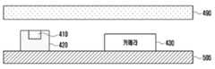
도 5를 참조하면, 본 발명의 다양한 실시예에 따른 전자 장치(400)는, PCB(405) 상에 발광부(410), 생체 센서(420) 및 카메라(430)가 구비될 수 있다. 상기 발광부(410), 생체 센서(420) 및 카메라(430) 상에는 동일한 투명 부재(490)가 배치될 수 있다. 일 실시예에 따르면 상기 발광부(410)는 생체 센서(420)의 내부에 구비될 수 있다. 상기 발광부(410)를 포함하는 생체 센서(420)와 카메라(430)는 PCB(505) 상의 제 1 방향(예: 수평)에 소정 거리만큼 이격되어 배치될 수 있다.Referring to FIG. 5 , in the
도 6은 본 발명의 다양한 실시예에 따른 전자 장치에 구비된 생체 센서의 구성을 나타내는 도면이다.6 is a diagram illustrating a configuration of a biometric sensor provided in an electronic device according to various embodiments of the present disclosure.
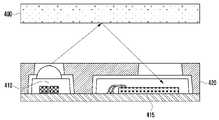
도 6을 참조하면, 본 발명의 다양한 실시예에 따른 전자 장치(400)의 생체 센서(420)는 투명 부재(490)의 하부에 배치될 수 있다. 상기 생체 센서(420)는 발광부(410) 및 수광부(415)를 포함할 수 있다. 즉, 상기 발광부(410) 및 수광부(415)는 하나의 생체 센서(420) 내부에 구비될 수 있다. 상기 발광부(410)가 생체 센서(410) 내부에 구비된 경우, 상기 발광부(410)를 통해 방사된 광은 투명 부재(490)를 통해 반사되어 수광부(415)에 수신될 수 있다. 프로세서(480)는 상기 수광부(415)에 수신된 광을 통해 상기 발광부(410)의 광량을 유추할 수 있다. 일 실시예에 따르면, 생체 센서(420)의 발광부(410)로부터 방사된 광은 투명 부재(490)를 통해 반사될 수 있다. 이 반사된 광은 생체 센서(420)의 수광부(415)(예: 포토 다이오드)에 입사될 수 있다. 이 입사된 광량의 값은 상기 발광부(410)의 광량에 비례할 수 있다. 상기 입사된 광량의 값은 스케일(scale)이 큰 값(예: 손가락 측정시 전체 광량의 대략 50~70% 정도)이므로, 상기 투명 부재(490)에 흡착된 이물질에 의한 반사량의 변화는 작은 비중을 차지할 수 있다. 예를 들어, 프로세서(480)는 상기 발광부(410)를 통해 방사된 광이 미리 설정된 기준값보다 크거나 작을 경우, 상기 발광부(410)의 전류를 제어하여 광량을 보정할 수 있다. 한편, 생체 센서(420)의 내부에 구비된 발광부(410)는 투명 부재(490)에 전반적으로 전반사를 일으켜 광의 특성상 넓게 퍼져 진행하도록 할 수 있다.Referring to FIG. 6 , the
도 7은 본 발명의 다양한 실시예에 따른 전자 장치의 후면의 일부 구성에 대한 다른 예를 나타내는 도면이다.7 is a diagram illustrating another example of a partial configuration of a rear surface of an electronic device according to various embodiments of the present disclosure;
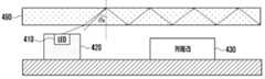
도 7을 참조하면, 본 발명의 다양한 실시예에 따른 전자 장치(400)의 발광부(410)는 생체 센서(420)의 내부에 실장되지 않고, 단독으로 구비될 수 있다. 상기 발광부(410)는 상기 카메라(430)와 소정 거리만큼 이격되어, 투명 부재(490)의 하부에 배치될 수 있다. 카메라(430)는 상기 발광부(410)에 대한 수광부로 동작할 수 있다. 이 경우, 발광부(410)는 카메라(430)에서 수신가능한 영역의 파장을 선택적으로 사용할 수 있다. 즉, 발광부(410)의 파장은 카메라(430) 픽셀의 컬러 필터를 통과 가능한 파장 영역의 일부를 포함할 수 있다. 예를 들어, 상기 발광부(410)는 약 880nm의 파장을 갖는 적외선(IR) LED, 약 660nm의 파장을 갖는 레드 LED, 약 550nm의 파장을 갖는 그린 LED 및 약 440nm의 파장을 갖는 블루 LED 중 적어도 하나를 포함할 수 있다.Referring to FIG. 7 , the
도 8은 본 발명의 다양한 실시예에 따른 전자 장치의 후면의 일부 구성에 대한 또 다른 예를 나타내는 도면이다.8 is a diagram illustrating another example of a partial configuration of a rear surface of an electronic device according to various embodiments of the present disclosure.
도 8을 참조하면, 본 발명의 다양한 실시예에 따른 전자 장치(400)는, 카메라 플래쉬(810), 생체 센서(420), 지문 센서(425), 제 1 카메라(430a), 제 2 카메라(430b) 및 투명 부재(490)를 포함할 수 있다. 상기 카메라 플래쉬(810)는 도 7에 도시된 발광부(410)의 기능을 수행할 수 있다. 일 실시예에 따르면, 도 7에 도시된 발광부(410)는 생체 센서(420) 내부에 포함될 수 있다.Referring to FIG. 8 , an
상기 제 1 카메라(430a) 및 제 2 카메라(430b)에 인접하여, 생체 센서(420) 또는 지문 센서(425)가 위치하게 되면, 사용자가 상기 생체 센서(420) 또는 지문 센서(425)를 터치하는 중에 제 1 카메라(430a) 및 제 2 카메라(430b) 상의 투명 부재(490)에 이물질(예: 지문 인식에 따른 손가락의 유분, 먼지 등)이 흡착될 수 있다. 예를 들어, 증강현실 (augmented reality; AR) 기술 또는 빅스비 비젼(bixby vision)(또는 비전 인텔리젼스(vision intelligence)) 등 정확하고 선명한 이미지를 획득하고, 상기 획득된 이미지에 대한 정보를 추출해야 하는 경우, 제 1 카메라(430a) 및 제 2 카메라(430b) 상의 투명 부재(490)에 이물질(예: 사용자 손가락의 유분 또는 먼지 등)이 흡착되면, 선명한 이미지를 획득하지 못할 수 있다. 예를 들어, 제 1 카메라(430a) 및 제 2 카메라(430b)를 포함하는 카메라(430) 상의 투명 부재(490)에 대한 이물질 흡착 정보를 전자 장치(400)의 사용자에게 통지하고, 이물질을 제거하게 하면, 선명한 이미지를 획득할 수 있다.When the
도 8을 참조하면, 상기 제 1 카메라(430a) (예: 도 4의 카메라가 듀얼 카메라로 구성될 경우)는 광각 카메라를 포함할 수 있다. 상기 제 2 카메라(430b)는 협각 카메라를 포함할 수 있다. 예를 들어, 상기 제 1 카메라(430a)가 온(on) 상태에서, 전자 장치(400)의 사용자가 줌인(zoom in)을 하게 되면, 제 1 카메라(430a)는 일정 크기까지 줌인 처리된 후, 일정 크기에 도달하면, 제 2 카메라(430b)로 오토 스위치가 이루어질 수 있다. 이 경우, 제 1 카메라(430a) 및 제 2 카메라(430b)는 전류 소모 이슈로 인해, 서로 다른 동작이 진행될 수 있다. 따라서, 본 발명의 다양한 실시예에서는, 줌인 비율에 따라 제 1 카메라(430a) 또는 제 2 카메라(430b) 중 하나를 선택적으로 온(on) 시킴으로써, 투명 부재(490) 상에 흡착된 이물질을 감지할 수 있다. 또한, 제 1 카메라(430a) 및 제 2 카메라(430b)를 동시 또는 순차적으로 온(on) 시킴으로써, 제 1 카메라(430a) 또는 제 2 카메라(430b) 중 어떤 카메라에 이물질이 흡착되었는지의 여부를 감지할 수 있다.Referring to FIG. 8 , the
일 실시예에 따르면, 도 7에 도시된 발광부(410) 또는 도 8에 도시된 카메라 플래쉬(810)는 제 1 카메라(430a) 및 제 2 카메라(430b)의 사이 또는 상부, 하부, 좌측부 및 우측부 등 이물질을 감지할 수 있는 소정 위치에 구비될 수 있다.According to an embodiment, the
도 9는 본 발명의 다양한 실시예에 따른 전자 장치의 발광부와 투명 부재 사이에 버퍼 윈도우가 배치된 예를 나타내는 도면이다.9 is a diagram illustrating an example in which a buffer window is disposed between a light emitting unit and a transparent member of an electronic device according to various embodiments of the present disclosure;
도 9를 참조하면, 본 발명의 다양한 실시예에 따른 전자 장치(400)의 발광부(410)와 투명 부재(490) 사이에는 버퍼 윈도우(494)가 배치될 수 있다. 예를 들어, 상기 버퍼 윈도우(494)는 투명 부재(490)의 하부에 결합되어, 발광부(410)로부터 방사된 광이 투명 부재(490)의 내부로 진행하여 전반사를 발생시킬 수 있도록 구성될 수 있다. 상기 버퍼 윈도우(494)는 발광부(410)로부터 방사된 광의 굴절되는 각도를 변경하여, 투명 부재(490)로의 광 유입을 도울 수 있다. 상기 버퍼 윈도우(494)는 투명 렌즈, 평판(flat) 렌즈 및 오목 렌즈 중 적어도 하나를 포함할 수 있다.Referring to FIG. 9 , a
도 10은 본 발명의 다양한 실시예에 따른 전자 장치의 발광부와 투명 부재 사이에 디퓨저(diffuser)가 배치된 예를 나타내는 도면이다.10 is a diagram illustrating an example in which a diffuser is disposed between a light emitting unit and a transparent member of an electronic device according to various embodiments of the present disclosure;
도 10을 참조하면, 본 발명의 다양한 실시예에 따른 전자 장치(400)의 발광부(410)와 투명 부재(490) 사이에는 디퓨저(496)가 배치될 수 있다. 예를 들어, 상기 디퓨저(496)는 발광부(410)의 상부에 결합되어, 발광부(410)로부터 방사된 광이 투명 부재(490)의 내부로 확산하여 전반사를 발생시킬 수 있도록 구성될 수 있다. 상기 디퓨저(496)는 발광부(410)로부터 방사된 광을 좌우 측면으로 확산시킴으로써, 투명 부재(490)로의 광 유입을 도울 수 있다.Referring to FIG. 10 , a
도 11은 본 발명의 다양한 실시예에 따른 전자 장치의 발광부와 투명 부재 사이에 회절광학소자(diffractive optical element; DOE)가 배치된 예를 나타내는 도면이다.11 is a diagram illustrating an example in which a diffractive optical element (DOE) is disposed between a light emitting unit and a transparent member of an electronic device according to various embodiments of the present disclosure;
도 11을 참조하면, 본 발명의 다양한 실시예에 따른 전자 장치(400)의 발광부(410)와 투명 부재(490) 사이에는 회절광학소자(DOE)(498)가 배치될 수 있다. 예를 들어, 상기 회절광학소자(DOE)(498)는 발광부(410)의 상부에 결합되어, 발광부(410)로부터 방사된 광이 투명 부재(490)의 내부로 진행하여 전반사를 발생시킬 수 있도록 구성될 수 있다. 상기 회절광학소자(DOE)(498)는 발광부(410)로부터 방사된 광을 한 방향으로 방사시킴으로써, 투명 부재(490)로의 광 유입을 도울 수 있다. 예를 들어, 회절광학소자(DOE)(498)는 광의 회절 특성을 이용하여, 광의 방향을 결정할 수 있는 필름(또는 레이어(layer))로 구성될 수 있다.Referring to FIG. 11 , a diffractive optical element (DOE) 498 may be disposed between the
도 12는 본 발명의 다양한 실시예에 따른 전자 장치의 전면의 일부 구성에 대한 일 예를 나타내는 도면이다.12 is a diagram illustrating an example of a partial configuration of a front surface of an electronic device according to various embodiments of the present disclosure;
도 12를 참조하면, 본 발명의 다양한 실시예에 따른 전자 장치(400)는, 제 1 카메라(432), 제 2 카메라(434 ) 및 투명 부재(490)를 포함할 수 있다. 제 1 카메라(432)는 RGB 카메라를 포함할 수 있다. 제 2 카메라(434)는 적외선(IR) 카메라를 포함할 수 있다. 제 2 카메라(434)는 적외선 발광부(434a) 및 적외선 수광부(434b)를 포함할 수 있다. 예를 들어 적외선 발광부(434a)로부터 방사된 광(light)은 제 1 카메라(432)의 필터를 통과 가능한 영역의 일부를 포함하거나, 적외선 수광부(434b)의 필터를 통과 가능한 영역의 일부를 포함할 수 있다. 이를 통해, 프로세서(480)는 제 1 카메라(432) 또는 제 2 카메라(434)의 적외선 수광부(434b) 상의 투명 부재(490)에 흡착된 이물질(예: 사용자 손가락의 유분 또는 먼지 등)을 감지할 수 있다.Referring to FIG. 12 , the
도 13은 본 발명의 다양한 실시예에 따른 전자 장치의 투명 부재에 대한 굴절률의 일 예를 설명하는 도면이다.13 is a view for explaining an example of a refractive index of a transparent member of an electronic device according to various embodiments of the present disclosure;
도 13을 참조하면, 본 발명의 다양한 실시예에 따른 전자 장치(400)는, 생체 센서(420)의 내부에 구비된 발광부(410)와, 수광부의 기능을 수행하는 카메라(430)를 통해 투명 부재(490)의 외부에 흡착된 이물질(예: 사용자 손가락의 유분 또는 먼지 등)을 감지할 수 있다. 예를 들어, 상기 발광부(410)를 통해 방사된 광은 다양한 경로를 통해 투명 부재(490)의 내부로 유입될 수 있다. 도 13을 참조하면, 상기 발광부(410)를 통해 방사된 광이 임계각(θc) 보다 큰 각도로 투명 부재(490)에 입사되면, 상기 임계각(θc) 보다 큰 각도로 입사되는 광은 전반사되어 카메라(430)로 향하지 않을 수 있다. 예를 들어, 약 660nm의 파장을 갖는 레드 LED에 대한 투명 부재(490)의 굴절률은 약 1.51이고, 외부 공기의 굴절률은 약 1.0이므로, 약 41.4° 이상의 광에 대하여 전반사 조건을 만족할 수 있다. 상기 전반사 조건은 가시광선 영역에서 그 차이가 매우 작을 수 있다. 예를 들어, 약 550nm의 파장을 갖는 그린 LED에 대한 투명 부재(490)의 굴절률은 1.512이고, 약 440nm의 파장을 갖는 블루 LED에 대한 투명 부재(490)의 굴절률은 1.513이고, 약 660nm의 파장을 갖는 레드 LED에 대한 투명 부재(490)의 굴절률은 1.511일 수 있다. 상기 굴절률은 각 파장 및 매질 별로 약간의 차이가 있을 수 있다. 예를 들어, 수분(물)의 굴절률은 1.33이고, 오일의 굴절률은 1.47이며, 글라스의 굴절률은 1.51이고, 플린트(flint) 글라스의 굴절률은 1.60이며, 은의 굴절률은 2.06이고, 다이아몬드의 굴절률은 2.42일 수 있다.Referring to FIG. 13 , the
도 14는 본 발명의 다양한 실시예에 따른 전자 장치의 투명 부재에 대한 굴절률의 다른 예를 설명하는 도면이다.14 is a view for explaining another example of a refractive index of a transparent member of an electronic device according to various embodiments of the present disclosure;
도 15를 참조하면, 발광부(410)로부터 투명 부재(490)로 방사된 광의 진행 방향에 있는 두 매질(제 1 매질(n1), 제 2 매질(n2))의 경계면에서는 다음의 수학식 1과 같은 공식(예: 스넬의 법칙)이 성립될 수 있다.Referring to FIG. 15 , at the interface between two media (the first medium n1 and the second medium n2 ) in the traveling direction of the light emitted from the
[수학식 1][ Equation 1]
n1sinθ1 = n2sinθ2n1 sinθ1 = n2 sinθ2
예를 들어, 공기(진공)는 굴절률이 1이므로, 공기의 굴절률을 기준으로 하면, 상기 발광부(410)로부터 투명 부재(490)로 방사된 광의 전반사가 일어나기 시작할 때의 입사각(임계각)은 다음의 수학식 2와 같은 공식이 성립될 수 있다.For example, since air (vacuum) has a refractive index of 1, based on the refractive index of air, the incident angle (critical angle) when total reflection of the light emitted from the
[수학식 2][ Equation 2]
sinθc = 1/nsinθc = 1/n
θc = sin-1(1/n)θc = sin-1 (1/n)
예를 들어, 투명 부재(490)의 굴절률은 1.51이므로, 상기 투명 부재(490)와 공기의 경계면에서의 입사각(임계각)은 다음의 수학식 3과 같은 공식이 성립될 수 있다. 즉, 입사각이 41.4° 이상인 광은 전반사 조건을 만족할 수 있다.For example, since the refractive index of the
[수학식 3][ Equation 3]
θ1 = θ2 = sin-1(1/1.51) = 41.4°θ1 = θ2 = sin-1 (1/1.51) = 41.4°
여기에서, 상기 투명 부재(490)에 대한 입사각(임계각)은 전자 장치(400)에 구비되는 윈도우 글라스 또는 커버 글라스의 한 종류이고, 이외에 다양한 매질을 갖는 부재가 전자 장치(400)에 구비될 수 있다. 예를 들어, 투명 부재(490)의 내부로부터 공기와의 경계면에 대해, 약 660nm의 파장을 갖는 레드 LED를 기준으로 할 때, 41.4°이상의 입사각을 갖는 광들은 모두 전반사를 통해 투명 부재(490)의 측면으로 빠져 나갈 수 있다. 이 투명 부재(490)의 측면으로 빠져 나간 광은 카메라(430)를 향해 진행하지 않을 수 있다.Here, the incident angle (critical angle) with respect to the
도 15는 본 발명의 다양한 실시예에 따른 전자 장치의 투명 부재 상에 흡착된 이물질을 감지하는 동작의 일 예를 설명하는 도면이다.15 is a view for explaining an example of an operation of detecting a foreign material adsorbed on a transparent member of an electronic device according to various embodiments of the present disclosure;
도 17을 참조하면, 투명 부재(490)의 외부에 오일 및 수분 등을 포함하는 지문과 같은 이물질(10)이 흡착될 수 있다. 이물질(10)의 굴절률은, 예를 들어, 오일의 굴절률인 1.47과, 수분(물)의 굴절률인 1.33을 가질 수 있다. 이 경우, 투명 부재(490)의 외부에 이물질이 흡착된 곳의 임계각(θc')은 이물질이 흡착되지 않은 곳의 임계각(θc)보다 클 수 있다. 예를 들어, 상기 투명 부재(490)의 내부로부터 이물질(10)과의 경계면에 대해 전반사를 만족시키는 임계각은 각각 78.5°(sin θ = 1.47/1.51)와 62.4°(sin θ = 1.33/1.51)를 가질 수 있다. 이 경우, 발광부(410)로부터 방사된 광 중, 78.5°와 62.4°보다 작은 입사각을 갖는 광들은 이물질(10) 내부로 투과할 수 있다. 상기 이물질(10) 내부로 투과된 광은 이물질(10) 내의 입자나, 투명 부재(490)와 이물질(10) 간의 경계면에서 반사를 일으키며 산란할 수 있다. 이 산란된 광은 카메라(430)를 향해 진행할 수 있다. 상기 산란된 광은 카메라(430)를 통해 촬영할 수 있다.Referring to FIG. 17 ,
도 16은 본 발명의 다양한 실시예에 따른 전자 장치의 투명 부재에 대한 이물질 유무 및 발광부의 온/오프에 따른 이미지를 설명하는 도면이다.16 is a view for explaining an image according to the presence or absence of a foreign material in a transparent member of an electronic device and on/off of a light emitting unit according to various embodiments of the present disclosure;
도 16을 참조하면, 투명 부재(490) 상의 이물질 흡착 유무 및 발광부(410)의 온/오프에 따라, 외부 객체에 대하여 획득된 이미지의 컬러는 상이할 수 있다. 예를 들어, 투명 부재(490) 상에 이물질이 흡착되지 않은 경우, 발광부(410)의 온/오프에 따라 촬영 및 획득된 이미지의 컬러 차이는 없을 수 있다. 그러나, 투명 부재(490) 상에 이물질(10)이 흡착된 경우, 발광부(410)의 온/오프에 따라 촬영 및 획득된 이미지는 컬러가 상이할 수 있다. 예를 들어, 투명 부재(490) 상에 이물질(10)이 흡착되어 있고, 발광부(410)가 오프인 경우, 이물질(10)이 흡착된 곳의 이미지는 뿌옇게 보일 수 있다. 또한, 투명 부재(490) 상에 이물질(10)이 흡착되어 있고, 발광부(410)가 온인 경우, 이물질(10)이 흡착된 곳의 이미지는 다른 영역의 이미지에 비해 컬러가 진하게 보일 수 있다.Referring to FIG. 16 , a color of an image acquired with respect to an external object may be different depending on whether foreign substances are adsorbed on the
도 17은 본 발명의 다양한 실시예에 따른 전자 장치의 투명 부재에 대한 이물질 유무 및 발광부의 온/오프에 따른 이미지의 컬러 정보 차이값을 설명하는 도면이다.17 is a view for explaining a difference value of color information of an image according to the presence or absence of a foreign substance in a transparent member of an electronic device and ON/OFF of a light emitting unit according to various embodiments of the present disclosure;
도 17을 참조하면, 투명 부재(490) 상의 이물질 흡착 유무 및 발광부(410)의 온/오프에 따라, 외부 객체에 대하여 획득된 이미지의 컬러 정보는 상이할 수 있다. 예를 들어, 투명 부재(490) 상에 이물질이 흡착되지 않은 경우, 발광부(410)의 온/오프에 따라 촬영 및 획득된 이미지의 컬러 정보 차이값은 0.44%일 수 있다. 즉, 투명 부재(490) 상에 이물질이 흡착되어 있지 않은 경우, 발광부(410)가 오프인 경우와 발광부(410)가 온인 경우에 획득된 이미지의 컬러 정보 차이값은 0.44%일 수 있다. 그러나, 투명 부재(490) 상에 이물질이 흡착된 경우, 발광부(410)의 온/오프에 따라 촬영 및 획득된 이미지의 컬러 정보 차이값은 4.41%일 수 있다. 즉, 투명 부재(490) 상이 이물질이 흡착된 경우, 발광부(410)가 오프인 경우와 발광부(410)가 온인 경우에 획득된 이미지의 컬러 정보 차이값은 4.41%일 수 있다. 상기 컬러 정보는 발광부(410)의 컬러에 따라 다르게 추출될 수 있다. 예를 들어, 상기 컬러 정보 차이값은 카메라(430)를 통해 촬영 및 획득된 전체 이미지에서 레드(red) 컬러 정보를 추출하여 모두 합산한 값일 수 있다. 또한, 상기 컬러 정보 차이값은 카메라(430)를 통해 촬영 및 획득된 전체 이미지에서 다른 컬러 정보(예: 블루 및 그린 등)를 추출하여 모두 합산한 값일 수 있다.Referring to FIG. 17 , color information of an image acquired with respect to an external object may be different depending on whether foreign substances are adsorbed on the
도 18은 본 발명의 다양한 실시예에 따른 전자 장치의 이미지에 대한 컬러 정보 차이를 설명하는 도면이다.18 is a diagram for explaining a difference in color information with respect to an image of an electronic device according to various embodiments of the present disclosure;
도 18을 참조하면, 제 1 이미지 영역(21)과 제 2 이미지 영역(22)을 중첩하는 공통 영역(23)을 통해, 제 1 이미지 영역(21)과 제 2 이미지 영역(22)에 대한 컬러 정보를 추출할 수 있다. 예를 들어, 카메라(430)를 통해 촬영된 제 1 이미지 및 제 2 이미지의 비교 시, 제 1 이미지 영역(21)과 제 2 이미지 영역(22)의 촬영 영역에 차이가 있는 경우, 투명 부재(490)에 이물질이 흡착되지 않았음에도 불구하고, 제 1 이미지 영역(21)과 제 2 이미지 영역(22) 간에 컬러 정보의 차이가 있을 수 있다. 이 경우, 제 1 이미지 영역(21)과 제 2 이미지 영역(22)에서 특징점을 찾고, 제 1 이미지 영역(21)과 제 2 이미지 영역(22)이 중첩되는 공통 영역(23)을 추출하여, 이 공통 영역(23)에 대한 컬러 정보를 추출할 수 있다. 예를 들어, 프로세서(480)의 비교 영역 정의부(482)는 카메라(430)를 통해 촬영된 적어도 2개 이상의 이미지에 대한 컬러 정보를 추출할 때, 상기 2개 이상의 이미지가 갖는 공통 영역을 정의할 수 있다. 상기 비교 영역 정의부(482)는 상기 2개 이상의 이미지에 대한 컬러 정보를 비교하기 위해, 공통적으로 촬영된 영역을 정의할 수 있다. 예를 들어, 비교 영역 정의부(482)는 카메라(430)를 통해 촬영된 적어도 2개 이상의 이미지의 공통 영역을 가속도 정보 등을 통해 추출할 수 있다. 비교 영역 정의부(482)는 첫번째 촬영된 이미지의 가속도 센서 정보와, 두번째 촬영된 이미지의 가속도 센서 정보를 바탕으로 움직임의 정도를 판단하고, 상기 움직임의 정도 만큼 공통 영역을 추출하는 알고리즘을 가지고 있을 수 있다. 일 실시예에 따르면, 상기 공통 영역은 메모리(470)에 저장된 기 설정된 영역값 일 수 있다. 다른 실시예에 따르면, 비교 영역 정의부(482)는 카메라(430)를 통해 촬영된 적어도 2개 이상의 이미지의 공통 영역을 카메라(430) 내의 인식기를 통해 식별할 수 있다. 예를 들어, 비교 영역 정의부(482)는 카메라(430)를 통해 촬영된 이미지가 풍경화인 경우 하늘 또는 땅을 식별할 수 있다. 비교 영역 정의부(482)는 카메라(430)를 통해 촬영된 이미지가 사람인 경우 얼굴 인식을 통해 동일인의 얼굴, 동일인의 옷 및 동일인의 기타 신체 중 적어도 하나를 식별할 수 있다. 비교 영역 정의부(482)는 카메라(430)를 통해 촬영된 이미지가 글씨 또는 바코드인 경우 글씨 또는 바코드를 추출해낸 영역을 식별할 수 있다. 비교 영역 정의부(482)는 카메라(430)를 통해 촬영된 이미지가 사물인 경우 가방, 책상, 스탠드 등을 식별할 수 있다.Referring to FIG. 18 , through the
도 19는 본 발명의 다양한 실시예에 따른 전자 장치를 통해 이물질 감지의 정확도를 높이는 일 예를 설명하는 도면이다.19 is a view for explaining an example of increasing the accuracy of detecting foreign substances through an electronic device according to various embodiments of the present disclosure;
도 19를 참조하면, 본 발명의 다양한 실시예에 따른 전자 장치(400)는, 발광부(410), 생체 센서(420), 제 1 카메라(430a), 제 2 카메라(430b) 및 투명 부재(490)를 포함할 수 있다.Referring to FIG. 19 , the
상기 제 1 카메라(430a) 및 제 2 카메라(430b)의 이물질 감지 영역이 광의 동일 경로 상에 있는 경우, 투명 부재(490)의 외부에 대한 이물질의 흡착 여부의 정확도를 높일 수 있다. 예를 들어, 발광부(410)와 더 가까이 있는 제 2 카메라(430b) 상의 투명 부재(490)에 이물질이 흡착된 경우, 발광부(410)로부터 더 멀리 있는 제 1 카메라(430a)로 진행하는 광의 양은 적어질 수 있다. 이로 인해, 발광부(410)로부터 더 멀리 있는 제 1 카메라(430a)를 통한 이물질 흡착 여부에 대한 정확도는 떨어질 수 있다. 따라서, 발광부(410)와 더 가까이 있는 제 2 카메라(430b) 상의 투명 부재(490)에 흡착된 이물질의 컬러 정보 차이값을 이용하여, 발광부(410)로부터 더 멀리 있는 제 1 카메라(430a)로 진행한 광의 양을 유추할 수 있다. 이를 통해, 발광부(410)로부터 더 멀리 있는 제 1 카메라(430a)가 이물질을 감지할 때의 신호를 보정하거나, 상기 제 1 카메라(430a)에 대한 발광부(410)의 광량을 조절하여 투명 부재(490) 상의 이물질의 흡착 여부에 대한 정확도를 높일 수 있다.When the foreign material detection areas of the
도 20은 본 발명의 다양한 실시예에 따른 전자 장치를 통해 이물질 감지의 정확도를 높이는 다른 예를 설명하는 도면이다.20 is a view for explaining another example of increasing the accuracy of detecting foreign substances through an electronic device according to various embodiments of the present disclosure;
도 20을 참조하면, 본 발명의 다양한 실시예에 따른 전자 장치(400)는 투명 부재(490) 상에 흡착된 이물질 감지의 정확도를 향상시키기 위해, 카메라(430)를 통해 촬영된 이미지를 구역(2010)별로 구획하여 분석할 수 있다. 상기와 같이 구획된 이미지에 대한 구역(2010)의 개수는 카메라(430)에 내장된 이미지 센서의 최대 픽셀수(예: 256개)까지 증가시킬 수 있다. 이와 같이, 이미지를 구역(2010) 별로 구획하여 분석하는 방법의 장점은 다음과 같다. 예를 들어, 발광부(410)로부터 방사된 광이 거울 등과 같이 반사율이 높은 피사체에 의해 직접 반사되어 돌아오는 경우, 투명 부재(490)에 이물질이 흡착되어 있지 않더라도, 소정 부분에서 컬러 정보의 차이가 크게 발생될 수 있다. 이 경우, 이미지의 소정 영역에 상기 반사에 대비하여 미리 설정한 기준값보다 큰 컬러 정보의 차이가 있을 때, 프로세서(490)는 상기 소정 영역에 대응하는 투명 부재(490) 상에 이물질이 흡착되지 않은 것으로 판단할 수 있다. 또한, 카메라(430)를 통해 촬영된 이미지에 대하여, 사용자가 인지하기 어려울 정도로 작은 이물질이 감지되거나, 이미지의 외곽에 이물질이 감지되어, 사용자가 이미지를 인식하는데 불편함이 없는 경우에는, 이를 무시하고 사용자에게 불필요한 이물질 흡착 여부를 통지하는 경우를 생략하게 할 수 있다. 또한, 이미지가 구역(2010)으로 구획되어 있으면, 투명 부재(490)에 홈(예: 스크래치) 등이 발생하여 촬영된 외부 객체(사진 및 동영상) 이미지의 특정 영역의 컬러를 제외시킬 때에도 편리할 수 있다. 또한, 이미지가 구역(2010)으로 구획되어 있으면, 투명 부재(490)에 홈이 존재하여, 촬영된 외부 객체(사진 및 동영상) 이미지의 특정 부분에서 지속적으로 화질이 이상한 경우, 프로세서(480)를 통해 흠이 존재하는 구역을 쉽게 검출할 수 있다.Referring to FIG. 20 , the
도 21은 본 발명의 다양한 실시예에 따른 전자 장치의 투명 부재 상에 이물질이 흡착된 것을 통지하는 일 예를 나타내는 도면이다.21 is a diagram illustrating an example of notifying that a foreign material is adsorbed on a transparent member of an electronic device according to various embodiments of the present disclosure;
도 21을 참조하면, 본 발명의 다양한 실시예에 따른 전자 장치(400)는 카메라(430) 상의 투명 부재(490)에 이물질(예: 사용자 손가락의 유분 또는 먼지 등)이 흡착된 경우, 이 감지된 흡착 정보를 통지하는 사용자 인터페이스(UI)를 디스플레이(440)를 통해 제공할 수 있다. 예를 들어, 상기 사용자 인터페이스(UI)는 카메라(430)의 상에 이물질이 흡착되었음을 알리는 경고 문구(예: 렌즈 상에 이물질이 많습니다 또는 이미지 왜곡이 발생할 수 있습니다 등)를 제공할 수 있다. 일 실시예에 따르면, 전자 장치(400)는 카메라(430) 상의 투명 부재(490)에 이물질이 흡착된 경우, 음성 또는 진동을 통해 전자 장치(400)의 사용자에게 알려줄 수 있다. 또한, 사용자 인터페이스(UI)는 바로 촬영 메뉴 또는 이물질을 제거하고 촬영할 수 있는 메뉴 등을 제공할 수 있다. 또한, 이미지가 구역(예: 도 20의 구역(2010))으로 구획되어 있는 경우, 어떤 구역에 이물질이 흡착되어 있는지를 전자 장치(400)의 사용자에게 사용자 인터페이스(UI)를 통해 알려줄 수 있다.Referring to FIG. 21 , the
도 22는 본 발명의 다양한 실시예에 따른 카메라를 구비할 수 있는 다양한 전자 장치를 설명하는 도면이다.22 is a view for explaining various electronic devices that may include a camera according to various embodiments of the present disclosure.
도 22에 도시된 전자 장치(2200)는 홈 허브(home hub), 수면 모니터링 관리 장치, 드론, 로봇 및 가전 제품(home appliances) 중 적어도 하나를 포함할 수 있다. 이외에도, 발광부(2210)(예: 본 발명의 다양한 실시예에 따른 발광부(410)) 및 카메라(2230)(예: 본 발명의 다양한 실시예에 따른 카메라(430))를 갖는 다른 전자 장치를 더 포함할 수 있다.The
다양한 실시예에 따르면, 상기 전자 장치(2200)에 구비된 카메라(2230)는 소정의 타겟을 모니터링하는 기능을 수행할 수 있다. 예를 들어, 상기 전자 장치(2200)가 홈 허브인 경우, 상기 카메라(2230)는 왕래하는 사람을 모니터링하는 장치이거나, 외부 침입을 감시하는 보안 관련 시큐리티 장치일 수 있다. 상기 전자 장치(2200)가 수면 모니터링 장치인 경우, 상기 카메라(2230)는 사용자의 수면 상태를 모니터링하는 장치일 수 있다. 상기 전자 장치(2200)가 냉장고인 경우, 상기 카메라(2230)는 냉장고의 내부 음식물을 모니터링하거나, 음식물의 존재 유무 또는 음식물의 유통기한 등을 알려 줄 수 있는 장치일 수 있다. 상기 전자 장치(2200)가 에어컨인 경우, 상기 카메라(2230)는 사용자의 위치를 모니터링하여, 모니터링된 사용자에게 시원한 바람이 갈 수 있도록 동작하는 장치일 수 있다. 상술한 다양한 전자 장치(4220)는 사용자가 카메라(2230)를 수시로 체크하고, 이물질을 제거하기가 어려울 수 있다. 즉, 본 발명의 다양한 실시예에 따른 발광부(2210)(예: 도 4의 발광부(410)) 및 카메라(2230)(예: 도 4의 카메라(430))를 이용하여, 이물질의 흡착 정보를 쉽게 감지할 수 있다. 다양한 실시예에 따르면, 이미지 프로세싱이 가능한 장치는, 발광부(2210)의 온/오프를 통해 각 이미지를 촬영하여, 각 이미지 정보를 비교하여, 비교 결과에 따른 컬러 정보의 차이를 사용자에게 제공할 수 있다. 이미지 프로세싱이 불가능한 장치는, 발광부(2210)의 온/오프를 통해 촬영된 각 이미지를 캡쳐하고, 이 캡쳐된 이미지들을 이미지 프로세싱이 가능한 장치(예: 모바일 단말, 서버 등)로 전송 및 비교하여 비교 결과에 따른 컬러 정보의 차이를 사용자에게 제공할 수 있다.According to various embodiments, the
도 23은 본 발명의 다양한 실시예에 따른 전자 장치가 카메라 상의 투명 부재에 대한 이물질 흡착 정보를 제공하는 일 예의 방법을 나타내는 흐름도이다.23 is a flowchart illustrating an example method in which an electronic device provides information on adsorption of foreign substances to a transparent member on a camera according to various embodiments of the present disclosure;
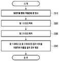
동작 2310에서, 카메라(430)의 촬영 모드가 시작되는 경우, 프로세서(460)는 발광부(410)를 통해 투명 부재(490)의 아래에 배치된 카메라(430)를 향하여 광을 방사할 수 있다.In
동작 2320에서, 프로세서(480)는 제 1 매질로 형성된 투명 부재(490)와, 상기 투명 부재(490)의 외부에 존재하는 제 2 매질 간의 광이 굴절되는 각도의 차이를 이용하여, 상기 발광부(410)로부터 방사된 상기 광의 일부가 상기 제 2 매질의 내부를 통해 전달되는 중에, 상기 카메라(430)를 이용하여 외부 객체에 대한 제 1 이미지를 획득할 수 있다. 이 경우, 상기 카메라(430)는 온 또는 오프를 통해 외부 객체에 대한 제 1 이미지를 획득할 수 있다.In
동작 2330에서, 프로세서(480)는 상기 카메라(430)를 이용하여 상기 외부 객체에 대한 제 2 이미지를 획득할 수 있다. 이 경우, 상기 카메라(430)는 오프 또는 온을 통해 외부 객체에 대한 제 2 이미지를 획득할 수 있다.In
동작 2340에서, 프로세서(480)는 상기 제 1 이미지의 적어도 일부 영역 및 상기 제 1 이미지의 상기 적어도 일부 영역에 대응하는 상기 제 2 이미지의 적어도 일부 영역 간의 컬러 차이를 이용하여, 상기 투명 부재(490)의 외면의 적어도 일부에 흡착된 제 3 매질의 이물질과 관련된 정보를 제공할 수 있다.In
상기 동작 2340에서, 프로세서(480)는 상기 이물질과 관련된 흡착 정보를 디스플레이(440)를 통한 사용자 인터페이스(UI), 오디오 출력부(450)를 통한 안내 음성 및 진동 출력부(460)를 통한 진동 중 적어도 하나를 이용하여 전자 장치(400)의 사용자에게 통지할 수 있다.In
일 실시예에 따르면, 프로세서(480)는 상기 카메라(430)를 통해 획득된 제 1 이미지 및 제 2 이미지의 공통 영역(예: 도 18의 공통 영역(23)(또는 비교 영역))을 추출할 수 있다. 상기 프로세서(480)는 상기 추출된 공통 영역에 대한 컬러 정보를 추출할 수 있다. 예를 들어, 카메라(430)를 통해 촬영된 제 1 이미지 및 제 2 이미지를 비교하고, 상기 제 1 이미지와 제 2 이미지의 촬영 영역에 컬러 차이가 있는 경우, 투명 부재(490)에 이물질이 흡착되지 않았음에도 불구하고, 제 1 이미지와 제 2 이미지 간에 컬러 정보의 차이가 있을 수 있다. 이 경우, 제 1 이미지와 제 2 이미지에서 특징점을 찾고, 상기 제 1 이미지와 제 2 이미지가 중첩되는 공통 영역을 추출하여, 이 공통 영역에 대한 컬러 정보를 추출할 수도 있다.According to an embodiment, the
도 24는 본 발명의 다양한 실시예에 따른 전자 장치가 카메라 상의 투명 부재에 대한 이물질 흡착 정보를 제공하는 다른 예의 방법을 나타내는 흐름도이다.24 is a flowchart illustrating another example method in which an electronic device provides information on adsorption of foreign substances to a transparent member on a camera according to various embodiments of the present disclosure;
동작 2410에서, 프로세서(480)는 카메라(430)를 이물질 감지 모드로 진입시킬 수 있다.In
동작 2420에서, 프로세서(480)는 카메라(430)의 노출(exposure)과 셔터 스피드(shutter speed)를 고정시킬 수 있다. 즉, 이물질 감지 모드 진입 시, 카메라(430)를 통해 촬영되는 이미지들의 컬러 정보를 비교하기 위해, 이미지의 노출과 셔터 스피드가 동일해야 하므로, 이를 고정시킬 수 있다. 이 경우, 각 이미지에 대한 피사체를 연속 촬영할 수 있도록 셔터 스피드는 빠를수록 좋으며, 해당 셔터 스피드에서 각 이미지의 컬러 정보가 포화(saturation)되지 않는 수준으로 노출을 설정할 수 있다.In
동작 2430에서, 프로세서(480)는 발광부(410)를 온(on)시키고, 카메라(430)를 이용하여 외부 객체에 대한 제 1 이미지를 획득할 수 있다.In
동작 2440에서, 프로세서(480)는 발광부(410)를 오프(off)시키고, 카메라(430)를 이용하여 외부 객체에 대한 제 2 이미지를 획득할 수 있다.In
동작 2450에서, 프로세서(480)는 상기 제 1 이미지와 제 2 이미지의 컬러 정보를 비교할 수 있다.In
동작 2460에서, 프로세서(480)는 상기 동작 2450의 비교 결과, 제 1 이미지 및 제 2 이미지의 컬러 정보의 차이가 기준값 이상인지의 여부를 판단할 수 있다.In
동작 2470에서, 프로세서(480)는 상기 동작 2460의 판단 결과, 컬러 정보의 차이가 기준값 이상이면, 카메라(430)의 외부에 이물질이 흡착된 것으로 판단하고, 이물질 흡착 정보를 디스플레이(440), 오디오 출력부(450) 및 진동 출력부(460) 중 적어도 하나를 이용하여 전자 장치(400)의 사용자에게 통지할 수 있다.In
동작 2480에서, 프로세서(480)는 상기 동작 2460의 판단 결과, 컬러 정보의 차이가 기준값 미만이면, 카메라(430)를 일반적인 촬영모드로 진입시킬 수 있다.In
상기 동작 2460에서, 제 1 이미지 및 제 2 이미지의 컬러 정보의 차이에 대한 기준값은 다음과 같은 수학식들을 통해 메모리(470)에 미리 설정될 수 있다.In
즉, 16비트 이미지인 경우, 카메라(430)의 1픽셀을 기준으로 한, 제 1 이미지 및 제 2 이미지의 컬러 정보의 차이에 대한 비율(%)은 다음의 수학식 4를 통해 구할 수 있다.That is, in the case of a 16-bit image, the ratio (%) of the difference between the color information of the first image and the second image based on one pixel of the
[수학식 4][ Equation 4]
비율(%) = 발광부 온(on) 상태에서 촬영된 이미지의 컬러 정보 - 발광부 오프(off) 상태에서 촬영된 이미지의 컬러 정보/256Ratio (%) = Color information of the image photographed with the emitter on - Color information of the image photographed with the emitter off/256
여기에서, 상기 256은 1픽셀을 기준으로 한 레드 컬러의 컬러 표현 범위인 0~255(2*16)=256 단계 일 수 있다.Here, 256 may be 0 to 255 (2* 16 ) = 256 steps, which is the color expression range of the red color based on 1 pixel.
또한, 16비트 이미지인 경우, 카메라(430)의 복수개의 픽셀을 기준으로 한, 제 1 이미지 및 제 2 이미지의 컬러 정보의 차이에 대한 비율(%)은 다음의 수학식 5를 통해 구할 수 있다.In addition, in the case of a 16-bit image, the ratio (%) of the difference between the color information of the first image and the second image based on a plurality of pixels of the
[수학식 5][ Equation 5]
비율(%) = 발광부 온(on) 상태에서 촬영된 이미지 분석영역에 대한 픽셀들의 컬러 정보 총합 - 발광부 오프(off) 상태에서 촬영된 이미지 분석영역에 대한 컬러 정보의 총합/256*분석 영역 내의 픽셀 개수Ratio (%) = Total color information of pixels for the image analysis area photographed with the light emitting unit on - Total color information for the image analysis area photographed with the light emitting unit off / 256*Analysis area number of pixels in
또한, 24비트 이미지인 경우, 카메라(430)의 1픽셀을 기준으로 한, 제 1 이미지 및 제 2 이미지의 컬러 정보의 차이에 대한 비율(%)은 다음의 수학식 6을 통해 구할 수 있다.Also, in the case of a 24-bit image, the ratio (%) of the difference between the color information of the first image and the second image based on one pixel of the
[수학식 6][ Equation 6]
비율(%) = 발광부 온(on) 상태에서 촬영된 이미지의 컬러 정보 - 발광부 오프(off) 상태에서 촬영된 이미지의 컬러 정보/2*24Ratio (%) = Color information of the image taken with the emitter on - Color information of the image shot with the emitter off/2*24
또한, 24비트 이미지인 경우, 카메라(430)의 복수개의 픽셀을 기준으로 한, 제 1 이미지 및 제 2 이미지의 컬러 정보의 차이에 대한 비율(%)은 다음의 수학식 7을 통해 구할 수 있다.In addition, in the case of a 24-bit image, the ratio (%) of the difference between the color information of the first image and the second image based on a plurality of pixels of the
[수학식 7][ Equation 7]
비율(%) = 발광부 온(on) 상태에서 촬영된 이미지 분석영역에 대한 픽셀들의 컬러 정보 총합 - 발광부 오프(off) 상태에서 촬영된 이미지 분석영역에 대한 컬러 정보의 총합/(2*24)*분석 영역 내의 픽셀 개수Ratio (%) = Total color information of pixels for the image analysis area photographed with the light emitting unit on - Total color information for the image analysis area photographed with the light emitting unit off / (2* 24 )*number of pixels in the analysis area
즉, 상술한 수학식 4 ~ 수학식 7을 통해 각각 추출된 비율이 특정 기준값(0.01 ~ 30%) 이상인 경우, 프로세서(480)는 카메라(430) 상의 투명 부재(490)에 이물질이 흡착된 것으로 판단할 수 있다.That is, when the ratios respectively extracted through Equations 4 to 7 are greater than or equal to a specific reference value (0.01 to 30%), the
도 25는 본 발명의 다양한 실시예에 따른 전자 장치가 카메라 상의 투명 부재에 대한 이물질 흡착을 측정하는 일 예의 방법을 나타내는 흐름도이다.25 is a flowchart illustrating an example method of measuring, by an electronic device, adsorption of foreign substances to a transparent member on a camera, according to various embodiments of the present disclosure;
동작 2510에서, 프로세서(480)는 이물질 감지 관련 어플리케이션이 실행되는 경우, 생체 센서(420)를 온(on)시킬 수 있다.In
동작 2520에서, 프로세서(480)는 생체 센서(420)를 통한 생체 정보 측정 모드인지 또는 이물질 측정 모드인지의 여부를 판단한 수 있다.In
동작 2530에서, 프로세서(480)는 상기 동작 2520의 판단 결과, 생체 정보 측정 모드이면, 생체 센서(420) 내부에 구비된 발광부(410)(예: 적외선 LED 및 레드 LED)의 광량을 설정할 수 있다. 예를 들어, 전자 장치(400) 사용자의 피부 상태에 따라 발광부(410)의 전류는 가변적으로 사용될 수 있다.In
동작 2540에서, 프로세서(480)는 상기 동작 2530에서 설정된 광량을 통해 전자 장치(400) 사용자의 생체 정보(예: 심박 수 및 혈압 등)를 측정할 수 있다.In
한편, 프로세서(480)는 상기 동작 2520의 판단 결과, 이물질 측정 모드이면, 동작 2550에서 생체 센서(420)를 이물질 측정 모드로 진입시키고, 동작 2560에서 카메라(430) 상의 투명 부재(490)에 흡착된 이물질을 측정할 수 있다.On the other hand, if it is determined in
상기 2560을 통해 이물질 측정 시, 프로세서(480)는 이물질 측정에 사용할 파장을 갖는 발광부(410)를 선택하여 전류값을 미리 설정된 값으로 고정시킬 수 있다. 또한, 프로세서(480)는 카메라(430)의 셔터 타이밍에 동기를 맞추어 발광부(410)를 온 시킨 상태에서 제 1 이미지를 획득하고, 발광부(410)를 오프 시킨 상태에서 제 2 이미지를 획득할 수 있다. 프로세서(480)는 발광부(410)를 선택적으로 온 시킬 수 있으므로 전자 장치(400)의 전류 소모를 줄일 수 있다. 프로세서(480)는 복수개의 발광부(410)를 온 시켜, 각각의 파장에 대한 이물질을 측정함으로써, 투명 부재(490) 상의 이물질 흡착에 대한 정확도를 높일 수 있다.When measuring the foreign material through the 2560, the
이상에서는 본 발명의 다양한 실시예에 따라 본 발명을 설명하였지만, 본 발명이 속하는 기술분야에서 통상의 지식을 가진 자가 본 발명의 기술적 사상을 벗어나지 않는 범위 내에서 변경 및 변형한 것도 본 발명에 속함은 당연하다.In the above, the present invention has been described according to various embodiments of the present invention, but changes and modifications made by those of ordinary skill in the art to which the present invention pertains without departing from the technical spirit of the present invention also belong to the present invention. Of course.
400: 전자 장치410: 발광부
420: 생체 센서430: 카메라
440: 디스플레이450: 오디오 출력부
460: 진동 출력부470: 메모리
480: 프로세서490: 투명 부재400: electronic device 410: light emitting unit
420: biometric sensor 430: camera
440: display 450: audio output
460: vibration output unit 470: memory
480: processor 490: transparent member
Claims (20)
Translated fromKorean투명 부재;
상기 투명 부재의 아래에 배치되고, 광을 방사하기 위한 발광부;
상기 투명 부재의 아래에 배치되고, 외부 객체에 대한 이미지를 획득하기 위한 카메라; 및
프로세서를 포함하고, 상기 프로세서는,
상기 발광부로부터 방사된 상기 광의 적어도 일부가 상기 투명 부재의 내부를 통해 전달되는 중에, 상기 카메라를 이용하여 상기 외부 객체에 대한 제 1 이미지 및 제 2 이미지를 획득하고;
상기 제 1 이미지의 적어도 일부 영역 및 상기 제 1 이미지의 상기 적어도 일부 영역에 대응하는 상기 제 2 이미지의 적어도 일부 영역 간의 컬러 차이를 이용하여, 상기 투명 부재의 외면의 적어도 일부에 흡착된 이물질 정보를 제공하되,
상기 외부 객체의 특정 부분에서 지속적으로 화질 이상이 검출되는 경우, 상기 투명 부재의 소정 위치에서 흠이 발생된 것을 알리는 정보를 제공하도록 설정된 전자 장치.In an electronic device,
transparent member;
a light emitting unit disposed under the transparent member and configured to emit light;
a camera disposed under the transparent member and configured to acquire an image of an external object; and
A processor comprising:
acquiring a first image and a second image of the external object by using the camera while at least a portion of the light emitted from the light emitting unit is transmitted through the inside of the transparent member;
Information on foreign substances adsorbed on at least a portion of the outer surface of the transparent member by using a color difference between at least a partial region of the first image and at least a partial region of the second image corresponding to the at least partial region of the first image provided, but
An electronic device configured to provide information indicating that a flaw has occurred at a predetermined position of the transparent member when an image quality abnormality is continuously detected in a specific portion of the external object.
상기 투명 부재는 렌즈(lens), 윈도우 글라스 및 커버 글라스 중 적어도 하나를 포함하는 전자 장치.The method of claim 1,
The transparent member includes at least one of a lens, a window glass, and a cover glass.
상기 투명 부재와 상기 발광부 사이에, 상기 광의 굴절되는 각도를 변경할 수 있는 다른 투명 부재를 더 포함하는 전자 장치.The method of claim 1,
The electronic device further comprising another transparent member capable of changing an angle at which the light is refracted between the transparent member and the light emitting part.
상기 발광부와 상기 카메라는 지정된 거리만큼 이격되어 배치된 전자 장치.The method of claim 1,
The light emitting unit and the camera are disposed to be spaced apart by a specified distance.
수광부를 더 포함하되,
상기 발광부와 상기 수광부는 하나의 생체 센서 내부에 구비된 전자 장치.The method of claim 1,
Further comprising a light receiving unit,
The light emitting unit and the light receiving unit are provided in one biosensor.
상기 프로세서는,
상기 이물질의 흡착 정보를 디스플레이를 통한 사용자 인터페이스(UI), 오디오 출력부를 통한 안내 음성 및 진동 출력부를 통한 진동 중 적어도 하나를 이용하여 제공하도록 설정된 전자 장치.The method of claim 1,
The processor is
An electronic device configured to provide the adsorption information of the foreign material using at least one of a user interface (UI) through a display, a guide voice through an audio output unit, and vibration through a vibration output unit.
메모리를 더 포함하되,
상기 프로세서는,
상기 투명 부재 상에 이물질이 흡착된 상태에서 이미지가 촬영된 경우, 이물질이 흡착된 이미지임을 알리는 태그를 부여하여 상기 메모리에 저장하도록 설정된 전자 장치.The method of claim 1,
further comprising memory,
The processor is
When an image is captured while a foreign material is adsorbed on the transparent member, a tag indicating that the foreign material is adsorbed is attached to the image and stored in the memory.
상기 프로세서(480)는,
상기 발광부를 통해 방사된 광이 미리 설정된 기준값보다 크거나 작을 경우, 상기 발광부의 전류를 제어하여 광량을 보정하도록 설정된 전자 장치.The method of claim 1,
The processor 480,
An electronic device configured to correct the amount of light by controlling the current of the light emitting unit when the light emitted through the light emitting unit is greater than or smaller than a preset reference value.
상기 다른 투명 부재는,
상기 투명 부재와 상기 발광부 사이에 구비된, 버퍼 윈도우, 디퓨저 및 회절광학소자(diffractive optical element; DOE) 중 적어도 하나를 포함하는 전자 장치.4. The method of claim 3,
The other transparent member,
and at least one of a buffer window, a diffuser, and a diffractive optical element (DOE) provided between the transparent member and the light emitting part.
발광부를 이용하여 투명 부재의 아래에 배치된 카메라를 향하여 광을 방사하는 동작;
프로세서가, 상기 발광부로부터 방사된 상기 광의 적어도 일부가 상기 투명 부재의 내부를 통해 전달되는 중에, 상기 카메라를 이용하여 외부 객체에 대한 제 1 이미지 및 제 2 이미지를 획득하는 동작;
상기 프로세서가 상기 제 1 이미지의 적어도 일부 영역 및 상기 제 1 이미지의 상기 적어도 일부 영역에 대응하는 상기 제 2 이미지의 적어도 일부 영역 간의 컬러 차이를 이용하여, 상기 투명 부재의 외면의 적어도 일부에 흡착된 이물질 정보를 제공하는 동작; 및
상기 외부 객체의 특정 부분에서 지속적으로 화질 이상이 검출되는 경우, 상기 투명 부재의 소정 위치에서 흠이 발생된 것을 알리는 정보를 제공하는 동작을 포함하는 방법.A method for providing information on adsorption of foreign substances in an electronic device, the method comprising:
emitting light toward a camera disposed under the transparent member using the light emitting unit;
obtaining, by the processor, a first image and a second image of an external object by using the camera while at least a portion of the light emitted from the light emitting unit is transmitted through the inside of the transparent member;
The processor uses a color difference between at least a partial region of the first image and at least a partial region of the second image corresponding to the at least partial region of the first image to be absorbed by at least a part of the outer surface of the transparent member providing foreign material information; and
and providing information indicating that a flaw has occurred at a predetermined position of the transparent member when an image quality abnormality is continuously detected in a specific portion of the external object.
상기 프로세서가, 상기 투명 부재와 상기 발광부 사이에 구비된 다른 투명 부재를 이용하여, 상기 광의 굴절되는 각도를 변경하는 동작을 더 포함하는 방법.12. The method of claim 11,
and changing, by the processor, an angle at which the light is refracted by using another transparent member provided between the transparent member and the light emitting unit.
상기 프로세서가, 상기 이물질의 흡착 정보를 디스플레이를 통한 사용자 인터페이스(UI), 오디오 출력부를 통한 안내 음성 및 진동 출력부를 통한 진동 중 적어도 하나를 이용하여 제공하는 동작을 더 포함하는 방법.12. The method of claim 11,
and providing, by the processor, the adsorption information of the foreign material using at least one of a user interface (UI) through a display, a guide voice through an audio output unit, and vibration through a vibration output unit.
상기 프로세서가, 상기 투명 부재 상에 이물질이 흡착된 상태에서 이미지가 촬영된 경우, 이물질이 흡착된 이미지임을 알리는 태그를 부여하여 메모리에 저장하는 동작을 더 포함하는 방법.12. The method of claim 11,
and, when the image is captured while the foreign material is adsorbed on the transparent member, by the processor, attaching a tag indicating that the foreign material is adsorbed to the image and storing the tag in the memory.
상기 프로세서가, 상기 발광부를 통해 방사된 광이 미리 설정된 기준값보다 크거나 작을 경우, 상기 발광부의 전류를 제어하여 광량을 보정하는 동작을 더 포함하는 방법.12. The method of claim 11,
and controlling, by the processor, a current of the light emitting unit to correct the amount of light when the light emitted through the light emitting unit is greater than or smaller than a preset reference value.
상기 프로세서가, 상기 제 1 이미지와 상기 제 2 이미지의 특징점을 찾고, 상기 제 1 이미지와 상기 제 2 이미지가 중첩되는 공통 영역을 추출하며, 상기 공통 영역에 대한 컬러 차이 정보를 추출하는 동작을 더 포함하는 방법.12. The method of claim 11,
an operation of, by the processor, finding feature points of the first image and the second image, extracting a common area where the first image and the second image overlap, and extracting color difference information for the common area How to include.
발광부를 이용하여 투명 부재의 아래에 배치된 카메라를 향하여 광을 방사하는 동작;
프로세서가, 상기 발광부로부터 방사된 상기 광의 적어도 일부가 상기 투명 부재의 내부를 통해 전달되는 중에, 상기 카메라를 이용하여 외부 객체에 대한 제 1 이미지 및 제 2 이미지를 획득하는 동작;
상기 프로세서가 상기 제 1 이미지의 적어도 일부 영역 및 상기 제 1 이미지의 상기 적어도 일부 영역에 대응하는 상기 제 2 이미지의 적어도 일부 영역 간의 컬러 차이를 이용하여, 상기 투명 부재의 외면의 적어도 일부에 흡착된 이물질 정보를 제공하는 동작; 및
상기 프로세서가, 상기 전자 장치의 이물질 감지 모드 진입 시, 상기 카메라의 노출(exposure) 및 셔터 스피드(shutter speed)를 고정시키는 동작을 더 포함하는 방법.A method for providing information on adsorption of foreign substances in an electronic device, the method comprising:
emitting light toward a camera disposed under the transparent member using the light emitting unit;
obtaining, by the processor, a first image and a second image of an external object by using the camera while at least a portion of the light emitted from the light emitting unit is transmitted through the inside of the transparent member;
The processor uses a color difference between at least a partial region of the first image and at least a partial region of the second image corresponding to the at least partial region of the first image to be absorbed by at least a part of the outer surface of the transparent member providing foreign material information; and
and fixing, by the processor, an exposure and a shutter speed of the camera when the electronic device enters a foreign material detection mode.
발광부를 이용하여 투명 부재의 아래에 배치된 카메라를 향하여 광을 방사하는 동작;
프로세서가, 상기 발광부로부터 방사된 상기 광의 적어도 일부가 상기 투명 부재의 내부를 통해 전달되는 중에, 상기 카메라를 이용하여 외부 객체에 대한 제 1 이미지 및 제 2 이미지를 획득하되, 상기 외부 객체에 대한 제 1 이미지는 상기 발광부가 온(on) 상태에서 획득되고, 상기 외부 객체에 대한 제 2 이미지는 상기 발광부가 오프(off) 상태에서 획득되는 동작; 및
상기 프로세서가 상기 제 1 이미지의 적어도 일부 영역 및 상기 제 1 이미지의 상기 적어도 일부 영역에 대응하는 상기 제 2 이미지의 적어도 일부 영역 간의 컬러 차이를 이용하여, 상기 투명 부재의 외면의 적어도 일부에 흡착된 이물질 정보를 제공하는 동작을 포함하는 방법.A method for providing information on adsorption of foreign substances in an electronic device, the method comprising:
emitting light toward a camera disposed under the transparent member using the light emitting unit;
A processor acquires a first image and a second image of an external object by using the camera while at least a portion of the light emitted from the light emitting unit is transmitted through the inside of the transparent member, an operation in which the first image is obtained in an on state of the light emitting unit, and the second image of the external object is obtained in an off state of the light emitting unit; and
The processor uses a color difference between at least a partial region of the first image and at least a partial region of the second image corresponding to the at least partial region of the first image to be absorbed by at least a part of the outer surface of the transparent member A method comprising providing foreign material information.
상기 발광부로부터 방사된 상기 광의 적어도 일부가 상기 투명 부재의 내부를 통해 전달되는 중에, 상기 카메라를 이용하여 상기 외부 객체에 대한 제 1 이미지 및 제 2 이미지를 획득하는 동작;
상기 제 1 이미지의 적어도 일부 영역 및 상기 제 1 이미지의 상기 적어도 일부 영역에 대응하는 상기 제 2 이미지의 적어도 일부 영역 간의 컬러 차이를 이용하여, 상기 투명 부재의 외면의 적어도 일부에 흡착된 이물질 정보를 제공하는 동작; 및
상기 외부 객체의 특정 부분에서 지속적으로 화질 이상이 검출되는 경우, 상기 투명 부재의 소정 위치에서 흠이 발생된 것을 알리는 정보를 제공하는 동작을 포함하는 방법을 수행하는 프로그램이 기록된 컴퓨터 판독 가능한 기록 매체.transparent member; a light emitting unit disposed under the transparent member and configured to emit light; a camera disposed under the transparent member and configured to acquire an image of an external object; and a computer-readable recording medium on which a program for performing a method for providing information on adsorption of foreign substances in an electronic device including a processor is recorded,
acquiring a first image and a second image of the external object by using the camera while at least a portion of the light emitted from the light emitting unit is transmitted through the inside of the transparent member;
Information on foreign substances adsorbed on at least a portion of the outer surface of the transparent member by using a color difference between at least a partial region of the first image and at least a partial region of the second image corresponding to the at least partial region of the first image action to provide; and
When an image quality abnormality is continuously detected in a specific portion of the external object, a computer-readable recording medium recording a program for performing a method including providing information indicating that a flaw has occurred at a predetermined position of the transparent member .
Priority Applications (4)
| Application Number | Priority Date | Filing Date | Title |
|---|---|---|---|
| KR1020170086661AKR102452065B1 (en) | 2017-07-07 | 2017-07-07 | Electronic device and method for providing adsorption information of foreign substance adsorbed to cemera |
| EP18828865.8AEP3635681A4 (en) | 2017-07-07 | 2018-05-30 | ELECTRONIC DEVICE AND METHOD FOR PROVIDING ADSORPTION INFORMATION ON A FOREIGN SUBSTANCE ADSORBED BY A CAMERA |
| PCT/KR2018/006155WO2019009520A1 (en) | 2017-07-07 | 2018-05-30 | Electronic device and method for providing adsorption information of foreign substance adsorbed by camera |
| US16/013,257US10547767B2 (en) | 2017-07-07 | 2018-06-20 | Electronic device and method for providing adsorption information of foreign substance adsorbed by camera |
Applications Claiming Priority (1)
| Application Number | Priority Date | Filing Date | Title |
|---|---|---|---|
| KR1020170086661AKR102452065B1 (en) | 2017-07-07 | 2017-07-07 | Electronic device and method for providing adsorption information of foreign substance adsorbed to cemera |
Publications (2)
| Publication Number | Publication Date |
|---|---|
| KR20190005657A KR20190005657A (en) | 2019-01-16 |
| KR102452065B1true KR102452065B1 (en) | 2022-10-11 |
Family
ID=64903024
Family Applications (1)
| Application Number | Title | Priority Date | Filing Date |
|---|---|---|---|
| KR1020170086661AActiveKR102452065B1 (en) | 2017-07-07 | 2017-07-07 | Electronic device and method for providing adsorption information of foreign substance adsorbed to cemera |
Country Status (4)
| Country | Link |
|---|---|
| US (1) | US10547767B2 (en) |
| EP (1) | EP3635681A4 (en) |
| KR (1) | KR102452065B1 (en) |
| WO (1) | WO2019009520A1 (en) |
Families Citing this family (4)
| Publication number | Priority date | Publication date | Assignee | Title |
|---|---|---|---|---|
| KR102390798B1 (en) | 2017-08-22 | 2022-04-26 | 삼성전자주식회사 | An electronic device providing graphical content and control method |
| JP2022096878A (en)* | 2020-12-18 | 2022-06-30 | Tdk株式会社 | Foreign object detection device, wireless power transmission device, and wireless power transmission system |
| CN113015278A (en)* | 2021-02-01 | 2021-06-22 | 惠而浦公司 | Transparent metal coating for camera panes in microwave ovens |
| WO2024071756A1 (en)* | 2022-09-27 | 2024-04-04 | 삼성전자주식회사 | Electronic device including sensor module and operating method thereof |
Citations (2)
| Publication number | Priority date | Publication date | Assignee | Title |
|---|---|---|---|---|
| JP2002374445A (en)* | 2001-06-12 | 2002-12-26 | Nikon Corp | Electronic camera |
| WO2012033005A1 (en)* | 2010-09-08 | 2012-03-15 | 日本電気株式会社 | Photographing device and photographing method |
Family Cites Families (10)
| Publication number | Priority date | Publication date | Assignee | Title |
|---|---|---|---|---|
| US5483346A (en)* | 1994-04-11 | 1996-01-09 | Butzer; Dane C. | Polarization based optical sensor utilizing total internal reflection |
| JP4326999B2 (en)* | 2003-08-12 | 2009-09-09 | 株式会社日立製作所 | Image processing system |
| EP1706730A1 (en)* | 2003-12-30 | 2006-10-04 | Agency for Science, Technology and Research | Method and apparatus for detection of inclusions in glass |
| KR100897223B1 (en)* | 2004-11-24 | 2009-05-14 | 아사히 가라스 가부시키가이샤 | Method and device for inspecting defect of transparent plate body |
| JP2008076113A (en)* | 2006-09-19 | 2008-04-03 | Ohara Inc | Surface flaw detection method and surface flaw inspection device |
| JP2011078047A (en)* | 2009-10-02 | 2011-04-14 | Sanyo Electric Co Ltd | Imaging apparatus |
| US8805302B2 (en)* | 2011-05-19 | 2014-08-12 | Apple Inc. | Proximity and ambient light sensor with improved smudge rejection |
| JP5999483B2 (en)* | 2011-11-02 | 2016-09-28 | 株式会社リコー | Adhering matter detection device and in-vehicle device control device |
| US9098124B2 (en) | 2013-01-10 | 2015-08-04 | Apple Inc. | Proximity sensors with smudge detection capabilities |
| KR102206877B1 (en)* | 2014-02-21 | 2021-01-26 | 삼성전자주식회사 | Method and apparatus for displaying biometric information |
- 2017
- 2017-07-07KRKR1020170086661Apatent/KR102452065B1/enactiveActive
- 2018
- 2018-05-30EPEP18828865.8Apatent/EP3635681A4/ennot_activeWithdrawn
- 2018-05-30WOPCT/KR2018/006155patent/WO2019009520A1/ennot_activeCeased
- 2018-06-20USUS16/013,257patent/US10547767B2/enactiveActive
Patent Citations (2)
| Publication number | Priority date | Publication date | Assignee | Title |
|---|---|---|---|---|
| JP2002374445A (en)* | 2001-06-12 | 2002-12-26 | Nikon Corp | Electronic camera |
| WO2012033005A1 (en)* | 2010-09-08 | 2012-03-15 | 日本電気株式会社 | Photographing device and photographing method |
Also Published As
| Publication number | Publication date |
|---|---|
| WO2019009520A1 (en) | 2019-01-10 |
| US20190014240A1 (en) | 2019-01-10 |
| US10547767B2 (en) | 2020-01-28 |
| EP3635681A1 (en) | 2020-04-15 |
| KR20190005657A (en) | 2019-01-16 |
| EP3635681A4 (en) | 2020-04-22 |
Similar Documents
| Publication | Publication Date | Title |
|---|---|---|
| KR102446849B1 (en) | Electronic device and method for identifying forgery of biometric information | |
| KR102786948B1 (en) | Proximity sensing apparatus in electronic device and method thereof | |
| KR102439245B1 (en) | Electronic device and its control method | |
| KR102666977B1 (en) | Electronic device and method for photographing image thereof | |
| KR102459243B1 (en) | Electronic device and method for photographing thereof | |
| KR102620138B1 (en) | Method for Outputting Screen and the Electronic Device supporting the same | |
| KR102319803B1 (en) | Electronic device, operating method thereof and recording medium | |
| KR102488563B1 (en) | Apparatus and Method for Processing Differential Beauty Effect | |
| US11159782B2 (en) | Electronic device and gaze tracking method of electronic device | |
| KR102401932B1 (en) | Electronic device measuring biometric information and method of operating the same | |
| KR20180091589A (en) | Method for providing skin information and electronic device supporting the same | |
| KR102685894B1 (en) | Electronic device for authenticating based on biometric data and operating method thereof | |
| KR102525126B1 (en) | Electronic device comprising iris camera | |
| KR20180061835A (en) | Electronic device and method for displaying image for iris recognition in electronic device | |
| KR102748020B1 (en) | Electronic device and method for determining underwater shooting | |
| KR102350497B1 (en) | Method for determining data of barometer sensor using data obtained from motion sensor and electronic device for the same | |
| KR102358849B1 (en) | Electronic device for providing information related to a smart watch and method for operating the same | |
| KR102773928B1 (en) | Method and device for acquiring information by capturing eye | |
| KR102368847B1 (en) | Method for outputting content corresponding to object and electronic device thereof | |
| KR20180022112A (en) | Electronic device including the iris recognition sensor and operating method thereof | |
| KR20170112278A (en) | Electronic device | |
| KR102452065B1 (en) | Electronic device and method for providing adsorption information of foreign substance adsorbed to cemera | |
| KR102477522B1 (en) | Electronic device and method for adjusting exposure of camera of the same | |
| KR102547054B1 (en) | Electronic device and method for controlling activation of camera module | |
| KR102656557B1 (en) | Image processing method and electronic device supporting the same |
Legal Events
| Date | Code | Title | Description |
|---|---|---|---|
| PA0109 | Patent application | Patent event code:PA01091R01D Comment text:Patent Application Patent event date:20170707 | |
| PG1501 | Laying open of application | ||
| A201 | Request for examination | ||
| PA0201 | Request for examination | Patent event code:PA02012R01D Patent event date:20200604 Comment text:Request for Examination of Application Patent event code:PA02011R01I Patent event date:20170707 Comment text:Patent Application | |
| E902 | Notification of reason for refusal | ||
| PE0902 | Notice of grounds for rejection | Comment text:Notification of reason for refusal Patent event date:20220215 Patent event code:PE09021S01D | |
| E701 | Decision to grant or registration of patent right | ||
| PE0701 | Decision of registration | Patent event code:PE07011S01D Comment text:Decision to Grant Registration Patent event date:20220825 | |
| GRNT | Written decision to grant | ||
| PR0701 | Registration of establishment | Comment text:Registration of Establishment Patent event date:20221004 Patent event code:PR07011E01D | |
| PR1002 | Payment of registration fee | Payment date:20221005 End annual number:3 Start annual number:1 | |
| PG1601 | Publication of registration |