KR102451650B1 - Stacked type seniconductor apparatus - Google Patents
Stacked type seniconductor apparatusDownload PDFInfo
- Publication number
- KR102451650B1 KR102451650B1KR1020160014917AKR20160014917AKR102451650B1KR 102451650 B1KR102451650 B1KR 102451650B1KR 1020160014917 AKR1020160014917 AKR 1020160014917AKR 20160014917 AKR20160014917 AKR 20160014917AKR 102451650 B1KR102451650 B1KR 102451650B1
- Authority
- KR
- South Korea
- Prior art keywords
- scan
- signal
- abandoned
- result value
- vias
- Prior art date
- Legal status (The legal status is an assumption and is not a legal conclusion. Google has not performed a legal analysis and makes no representation as to the accuracy of the status listed.)
- Active
Links
Images


Classifications
- G—PHYSICS
- G11—INFORMATION STORAGE
- G11C—STATIC STORES
- G11C29/00—Checking stores for correct operation ; Subsequent repair; Testing stores during standby or offline operation
- G11C29/04—Detection or location of defective memory elements, e.g. cell constructio details, timing of test signals
- G11C29/08—Functional testing, e.g. testing during refresh, power-on self testing [POST] or distributed testing
- G11C29/12—Built-in arrangements for testing, e.g. built-in self testing [BIST] or interconnection details
- G11C29/44—Indication or identification of errors, e.g. for repair
- G—PHYSICS
- G01—MEASURING; TESTING
- G01R—MEASURING ELECTRIC VARIABLES; MEASURING MAGNETIC VARIABLES
- G01R31/00—Arrangements for testing electric properties; Arrangements for locating electric faults; Arrangements for electrical testing characterised by what is being tested not provided for elsewhere
- G01R31/28—Testing of electronic circuits, e.g. by signal tracer
- G01R31/317—Testing of digital circuits
- G01R31/3181—Functional testing
- G01R31/3185—Reconfiguring for testing, e.g. LSSD, partitioning
- G01R31/318533—Reconfiguring for testing, e.g. LSSD, partitioning using scanning techniques, e.g. LSSD, Boundary Scan, JTAG
- G—PHYSICS
- G01—MEASURING; TESTING
- G01R—MEASURING ELECTRIC VARIABLES; MEASURING MAGNETIC VARIABLES
- G01R31/00—Arrangements for testing electric properties; Arrangements for locating electric faults; Arrangements for electrical testing characterised by what is being tested not provided for elsewhere
- G01R31/28—Testing of electronic circuits, e.g. by signal tracer
- G01R31/317—Testing of digital circuits
- G01R31/31723—Hardware for routing the test signal within the device under test to the circuits to be tested, e.g. multiplexer for multiple core testing, accessing internal nodes
- G—PHYSICS
- G01—MEASURING; TESTING
- G01R—MEASURING ELECTRIC VARIABLES; MEASURING MAGNETIC VARIABLES
- G01R31/00—Arrangements for testing electric properties; Arrangements for locating electric faults; Arrangements for electrical testing characterised by what is being tested not provided for elsewhere
- G01R31/28—Testing of electronic circuits, e.g. by signal tracer
- G01R31/2851—Testing of integrated circuits [IC]
- G01R31/2855—Environmental, reliability or burn-in testing
- G01R31/2872—Environmental, reliability or burn-in testing related to electrical or environmental aspects, e.g. temperature, humidity, vibration, nuclear radiation
- G01R31/2879—Environmental, reliability or burn-in testing related to electrical or environmental aspects, e.g. temperature, humidity, vibration, nuclear radiation related to electrical aspects, e.g. to voltage or current supply or stimuli or to electrical loads
- G—PHYSICS
- G01—MEASURING; TESTING
- G01R—MEASURING ELECTRIC VARIABLES; MEASURING MAGNETIC VARIABLES
- G01R31/00—Arrangements for testing electric properties; Arrangements for locating electric faults; Arrangements for electrical testing characterised by what is being tested not provided for elsewhere
- G01R31/28—Testing of electronic circuits, e.g. by signal tracer
- G01R31/2851—Testing of integrated circuits [IC]
- G01R31/2884—Testing of integrated circuits [IC] using dedicated test connectors, test elements or test circuits on the IC under test
- G—PHYSICS
- G01—MEASURING; TESTING
- G01R—MEASURING ELECTRIC VARIABLES; MEASURING MAGNETIC VARIABLES
- G01R31/00—Arrangements for testing electric properties; Arrangements for locating electric faults; Arrangements for electrical testing characterised by what is being tested not provided for elsewhere
- G01R31/28—Testing of electronic circuits, e.g. by signal tracer
- G01R31/317—Testing of digital circuits
- G01R31/3177—Testing of logic operation, e.g. by logic analysers
- G—PHYSICS
- G01—MEASURING; TESTING
- G01R—MEASURING ELECTRIC VARIABLES; MEASURING MAGNETIC VARIABLES
- G01R31/00—Arrangements for testing electric properties; Arrangements for locating electric faults; Arrangements for electrical testing characterised by what is being tested not provided for elsewhere
- G01R31/28—Testing of electronic circuits, e.g. by signal tracer
- G01R31/317—Testing of digital circuits
- G01R31/3181—Functional testing
- G01R31/3185—Reconfiguring for testing, e.g. LSSD, partitioning
- G01R31/318505—Test of Modular systems, e.g. Wafers, MCM's
- G01R31/318513—Test of Multi-Chip-Moduls
- G—PHYSICS
- G01—MEASURING; TESTING
- G01R—MEASURING ELECTRIC VARIABLES; MEASURING MAGNETIC VARIABLES
- G01R31/00—Arrangements for testing electric properties; Arrangements for locating electric faults; Arrangements for electrical testing characterised by what is being tested not provided for elsewhere
- G01R31/28—Testing of electronic circuits, e.g. by signal tracer
- G01R31/317—Testing of digital circuits
- G01R31/3181—Functional testing
- G01R31/3185—Reconfiguring for testing, e.g. LSSD, partitioning
- G01R31/318533—Reconfiguring for testing, e.g. LSSD, partitioning using scanning techniques, e.g. LSSD, Boundary Scan, JTAG
- G01R31/318536—Scan chain arrangements, e.g. connections, test bus, analog signals
- G01R31/318538—Topological or mechanical aspects
- G—PHYSICS
- G11—INFORMATION STORAGE
- G11C—STATIC STORES
- G11C29/00—Checking stores for correct operation ; Subsequent repair; Testing stores during standby or offline operation
- G11C29/56—External testing equipment for static stores, e.g. automatic test equipment [ATE]; Interfaces therefor
- G11C29/56008—Error analysis, representation of errors
- G—PHYSICS
- G11—INFORMATION STORAGE
- G11C—STATIC STORES
- G11C29/00—Checking stores for correct operation ; Subsequent repair; Testing stores during standby or offline operation
- G11C29/70—Masking faults in memories by using spares or by reconfiguring
- G11C29/88—Masking faults in memories by using spares or by reconfiguring with partially good memories
- G11C29/883—Masking faults in memories by using spares or by reconfiguring with partially good memories using a single defective memory device with reduced capacity, e.g. half capacity
- H—ELECTRICITY
- H01—ELECTRIC ELEMENTS
- H01L—SEMICONDUCTOR DEVICES NOT COVERED BY CLASS H10
- H01L22/00—Testing or measuring during manufacture or treatment; Reliability measurements, i.e. testing of parts without further processing to modify the parts as such; Structural arrangements therefor
- H01L22/20—Sequence of activities consisting of a plurality of measurements, corrections, marking or sorting steps
- H01L22/22—Connection or disconnection of sub-entities or redundant parts of a device in response to a measurement
- H—ELECTRICITY
- H01—ELECTRIC ELEMENTS
- H01L—SEMICONDUCTOR DEVICES NOT COVERED BY CLASS H10
- H01L22/00—Testing or measuring during manufacture or treatment; Reliability measurements, i.e. testing of parts without further processing to modify the parts as such; Structural arrangements therefor
- H01L22/30—Structural arrangements specially adapted for testing or measuring during manufacture or treatment, or specially adapted for reliability measurements
- H—ELECTRICITY
- H01—ELECTRIC ELEMENTS
- H01L—SEMICONDUCTOR DEVICES NOT COVERED BY CLASS H10
- H01L23/00—Details of semiconductor or other solid state devices
- H01L23/48—Arrangements for conducting electric current to or from the solid state body in operation, e.g. leads, terminal arrangements ; Selection of materials therefor
- H01L23/481—Internal lead connections, e.g. via connections, feedthrough structures
- H—ELECTRICITY
- H01—ELECTRIC ELEMENTS
- H01L—SEMICONDUCTOR DEVICES NOT COVERED BY CLASS H10
- H01L25/00—Assemblies consisting of a plurality of semiconductor or other solid state devices
- H01L25/03—Assemblies consisting of a plurality of semiconductor or other solid state devices all the devices being of a type provided for in a single subclass of subclasses H10B, H10D, H10F, H10H, H10K or H10N, e.g. assemblies of rectifier diodes
- H01L25/04—Assemblies consisting of a plurality of semiconductor or other solid state devices all the devices being of a type provided for in a single subclass of subclasses H10B, H10D, H10F, H10H, H10K or H10N, e.g. assemblies of rectifier diodes the devices not having separate containers
- H01L25/065—Assemblies consisting of a plurality of semiconductor or other solid state devices all the devices being of a type provided for in a single subclass of subclasses H10B, H10D, H10F, H10H, H10K or H10N, e.g. assemblies of rectifier diodes the devices not having separate containers the devices being of a type provided for in group H10D89/00
- H01L25/0657—Stacked arrangements of devices
- H—ELECTRICITY
- H01—ELECTRIC ELEMENTS
- H01L—SEMICONDUCTOR DEVICES NOT COVERED BY CLASS H10
- H01L25/00—Assemblies consisting of a plurality of semiconductor or other solid state devices
- H01L25/03—Assemblies consisting of a plurality of semiconductor or other solid state devices all the devices being of a type provided for in a single subclass of subclasses H10B, H10D, H10F, H10H, H10K or H10N, e.g. assemblies of rectifier diodes
- H01L25/04—Assemblies consisting of a plurality of semiconductor or other solid state devices all the devices being of a type provided for in a single subclass of subclasses H10B, H10D, H10F, H10H, H10K or H10N, e.g. assemblies of rectifier diodes the devices not having separate containers
- H01L25/07—Assemblies consisting of a plurality of semiconductor or other solid state devices all the devices being of a type provided for in a single subclass of subclasses H10B, H10D, H10F, H10H, H10K or H10N, e.g. assemblies of rectifier diodes the devices not having separate containers the devices being of a type provided for in group subclass H10D
- H01L25/073—Apertured devices mounted on one or more rods passed through the apertures
- H—ELECTRICITY
- H01—ELECTRIC ELEMENTS
- H01L—SEMICONDUCTOR DEVICES NOT COVERED BY CLASS H10
- H01L2224/00—Indexing scheme for arrangements for connecting or disconnecting semiconductor or solid-state bodies and methods related thereto as covered by H01L24/00
- H01L2224/01—Means for bonding being attached to, or being formed on, the surface to be connected, e.g. chip-to-package, die-attach, "first-level" interconnects; Manufacturing methods related thereto
- H01L2224/10—Bump connectors; Manufacturing methods related thereto
- H01L2224/12—Structure, shape, material or disposition of the bump connectors prior to the connecting process
- H01L2224/13—Structure, shape, material or disposition of the bump connectors prior to the connecting process of an individual bump connector
- H01L2224/13001—Core members of the bump connector
- H01L2224/1302—Disposition
- H01L2224/13025—Disposition the bump connector being disposed on a via connection of the semiconductor or solid-state body
- H—ELECTRICITY
- H01—ELECTRIC ELEMENTS
- H01L—SEMICONDUCTOR DEVICES NOT COVERED BY CLASS H10
- H01L2224/00—Indexing scheme for arrangements for connecting or disconnecting semiconductor or solid-state bodies and methods related thereto as covered by H01L24/00
- H01L2224/01—Means for bonding being attached to, or being formed on, the surface to be connected, e.g. chip-to-package, die-attach, "first-level" interconnects; Manufacturing methods related thereto
- H01L2224/10—Bump connectors; Manufacturing methods related thereto
- H01L2224/15—Structure, shape, material or disposition of the bump connectors after the connecting process
- H01L2224/16—Structure, shape, material or disposition of the bump connectors after the connecting process of an individual bump connector
- H01L2224/161—Disposition
- H01L2224/16135—Disposition the bump connector connecting between different semiconductor or solid-state bodies, i.e. chip-to-chip
- H01L2224/16145—Disposition the bump connector connecting between different semiconductor or solid-state bodies, i.e. chip-to-chip the bodies being stacked
- H01L2224/16146—Disposition the bump connector connecting between different semiconductor or solid-state bodies, i.e. chip-to-chip the bodies being stacked the bump connector connecting to a via connection in the semiconductor or solid-state body
- H—ELECTRICITY
- H01—ELECTRIC ELEMENTS
- H01L—SEMICONDUCTOR DEVICES NOT COVERED BY CLASS H10
- H01L2224/00—Indexing scheme for arrangements for connecting or disconnecting semiconductor or solid-state bodies and methods related thereto as covered by H01L24/00
- H01L2224/01—Means for bonding being attached to, or being formed on, the surface to be connected, e.g. chip-to-package, die-attach, "first-level" interconnects; Manufacturing methods related thereto
- H01L2224/10—Bump connectors; Manufacturing methods related thereto
- H01L2224/15—Structure, shape, material or disposition of the bump connectors after the connecting process
- H01L2224/17—Structure, shape, material or disposition of the bump connectors after the connecting process of a plurality of bump connectors
- H01L2224/171—Disposition
- H01L2224/1718—Disposition being disposed on at least two different sides of the body, e.g. dual array
- H01L2224/17181—On opposite sides of the body
- H—ELECTRICITY
- H01—ELECTRIC ELEMENTS
- H01L—SEMICONDUCTOR DEVICES NOT COVERED BY CLASS H10
- H01L2225/00—Details relating to assemblies covered by the group H01L25/00 but not provided for in its subgroups
- H01L2225/03—All the devices being of a type provided for in the same main group of the same subclass of class H10, e.g. assemblies of rectifier diodes
- H01L2225/04—All the devices being of a type provided for in the same main group of the same subclass of class H10, e.g. assemblies of rectifier diodes the devices not having separate containers
- H01L2225/065—All the devices being of a type provided for in the same main group of the same subclass of class H10
- H01L2225/06503—Stacked arrangements of devices
- H01L2225/06513—Bump or bump-like direct electrical connections between devices, e.g. flip-chip connection, solder bumps
- H—ELECTRICITY
- H01—ELECTRIC ELEMENTS
- H01L—SEMICONDUCTOR DEVICES NOT COVERED BY CLASS H10
- H01L2225/00—Details relating to assemblies covered by the group H01L25/00 but not provided for in its subgroups
- H01L2225/03—All the devices being of a type provided for in the same main group of the same subclass of class H10, e.g. assemblies of rectifier diodes
- H01L2225/04—All the devices being of a type provided for in the same main group of the same subclass of class H10, e.g. assemblies of rectifier diodes the devices not having separate containers
- H01L2225/065—All the devices being of a type provided for in the same main group of the same subclass of class H10
- H01L2225/06503—Stacked arrangements of devices
- H01L2225/06527—Special adaptation of electrical connections, e.g. rewiring, engineering changes, pressure contacts, layout
- H—ELECTRICITY
- H01—ELECTRIC ELEMENTS
- H01L—SEMICONDUCTOR DEVICES NOT COVERED BY CLASS H10
- H01L2225/00—Details relating to assemblies covered by the group H01L25/00 but not provided for in its subgroups
- H01L2225/03—All the devices being of a type provided for in the same main group of the same subclass of class H10, e.g. assemblies of rectifier diodes
- H01L2225/04—All the devices being of a type provided for in the same main group of the same subclass of class H10, e.g. assemblies of rectifier diodes the devices not having separate containers
- H01L2225/065—All the devices being of a type provided for in the same main group of the same subclass of class H10
- H01L2225/06503—Stacked arrangements of devices
- H01L2225/06541—Conductive via connections through the device, e.g. vertical interconnects, through silicon via [TSV]
- H01L2225/06544—Design considerations for via connections, e.g. geometry or layout
- H—ELECTRICITY
- H01—ELECTRIC ELEMENTS
- H01L—SEMICONDUCTOR DEVICES NOT COVERED BY CLASS H10
- H01L2225/00—Details relating to assemblies covered by the group H01L25/00 but not provided for in its subgroups
- H01L2225/03—All the devices being of a type provided for in the same main group of the same subclass of class H10, e.g. assemblies of rectifier diodes
- H01L2225/04—All the devices being of a type provided for in the same main group of the same subclass of class H10, e.g. assemblies of rectifier diodes the devices not having separate containers
- H01L2225/065—All the devices being of a type provided for in the same main group of the same subclass of class H10
- H01L2225/06503—Stacked arrangements of devices
- H01L2225/06555—Geometry of the stack, e.g. form of the devices, geometry to facilitate stacking
- H01L2225/06565—Geometry of the stack, e.g. form of the devices, geometry to facilitate stacking the devices having the same size and there being no auxiliary carrier between the devices
- H—ELECTRICITY
- H01—ELECTRIC ELEMENTS
- H01L—SEMICONDUCTOR DEVICES NOT COVERED BY CLASS H10
- H01L2225/00—Details relating to assemblies covered by the group H01L25/00 but not provided for in its subgroups
- H01L2225/03—All the devices being of a type provided for in the same main group of the same subclass of class H10, e.g. assemblies of rectifier diodes
- H01L2225/04—All the devices being of a type provided for in the same main group of the same subclass of class H10, e.g. assemblies of rectifier diodes the devices not having separate containers
- H01L2225/065—All the devices being of a type provided for in the same main group of the same subclass of class H10
- H01L2225/06503—Stacked arrangements of devices
- H01L2225/06596—Structural arrangements for testing
- H—ELECTRICITY
- H01—ELECTRIC ELEMENTS
- H01L—SEMICONDUCTOR DEVICES NOT COVERED BY CLASS H10
- H01L24/00—Arrangements for connecting or disconnecting semiconductor or solid-state bodies; Methods or apparatus related thereto
- H01L24/01—Means for bonding being attached to, or being formed on, the surface to be connected, e.g. chip-to-package, die-attach, "first-level" interconnects; Manufacturing methods related thereto
- H01L24/10—Bump connectors ; Manufacturing methods related thereto
- H01L24/12—Structure, shape, material or disposition of the bump connectors prior to the connecting process
- H01L24/13—Structure, shape, material or disposition of the bump connectors prior to the connecting process of an individual bump connector
- H—ELECTRICITY
- H01—ELECTRIC ELEMENTS
- H01L—SEMICONDUCTOR DEVICES NOT COVERED BY CLASS H10
- H01L24/00—Arrangements for connecting or disconnecting semiconductor or solid-state bodies; Methods or apparatus related thereto
- H01L24/01—Means for bonding being attached to, or being formed on, the surface to be connected, e.g. chip-to-package, die-attach, "first-level" interconnects; Manufacturing methods related thereto
- H01L24/10—Bump connectors ; Manufacturing methods related thereto
- H01L24/15—Structure, shape, material or disposition of the bump connectors after the connecting process
- H01L24/16—Structure, shape, material or disposition of the bump connectors after the connecting process of an individual bump connector
- H—ELECTRICITY
- H01—ELECTRIC ELEMENTS
- H01L—SEMICONDUCTOR DEVICES NOT COVERED BY CLASS H10
- H01L24/00—Arrangements for connecting or disconnecting semiconductor or solid-state bodies; Methods or apparatus related thereto
- H01L24/01—Means for bonding being attached to, or being formed on, the surface to be connected, e.g. chip-to-package, die-attach, "first-level" interconnects; Manufacturing methods related thereto
- H01L24/10—Bump connectors ; Manufacturing methods related thereto
- H01L24/15—Structure, shape, material or disposition of the bump connectors after the connecting process
- H01L24/17—Structure, shape, material or disposition of the bump connectors after the connecting process of a plurality of bump connectors
- H—ELECTRICITY
- H10—SEMICONDUCTOR DEVICES; ELECTRIC SOLID-STATE DEVICES NOT OTHERWISE PROVIDED FOR
- H10B—ELECTRONIC MEMORY DEVICES
- H10B20/00—Read-only memory [ROM] devices
- H10B20/20—Programmable ROM [PROM] devices comprising field-effect components
- H10B20/25—One-time programmable ROM [OTPROM] devices, e.g. using electrically-fusible links
Landscapes
- Engineering & Computer Science (AREA)
- Physics & Mathematics (AREA)
- General Physics & Mathematics (AREA)
- General Engineering & Computer Science (AREA)
- Microelectronics & Electronic Packaging (AREA)
- Power Engineering (AREA)
- Computer Hardware Design (AREA)
- Condensed Matter Physics & Semiconductors (AREA)
- Computer Networks & Wireless Communication (AREA)
- Manufacturing & Machinery (AREA)
- Tests Of Electronic Circuits (AREA)
- Semiconductor Integrated Circuits (AREA)
- Environmental & Geological Engineering (AREA)
- Health & Medical Sciences (AREA)
- Toxicology (AREA)
Abstract
Translated fromKoreanDescription
Translated fromKorean본 발명은 반도체 회로에 관한 것으로서, 특히 적층형 반도체 장치에 관한 것이다.BACKGROUND OF THE
적층형 반도체 장치는 관통 비아를 이용하여 적층된 반도체 칩들의 신호 전달이 이루어지도록 구성될 수 있다.The stacked semiconductor device may be configured to transmit signals between stacked semiconductor chips using through vias.
따라서 관통 비아의 불량이 발생할 경우, 정상적인 신호 전달이 어려우므로 이를 정확히 검출하고 그에 따라 불량이 발생한 관통 비아를 정상적인 관통 비아로 대체하는 리페어 동작이 필요하다.Therefore, when a defect occurs in a through-via, it is difficult to transmit a normal signal, so a repair operation is required to accurately detect the defect and replace the defective through-via with a normal through-via.
본 발명의 실시예는 관통 비아의 불량 검출 및 그에 따른 리페어 동작의 정확도를 향상시키고 불량 검출 및 리페어 동작에 소요되는 시간을 줄일 수 있는 적층형 반도체 장치를 제공한다.SUMMARY OF THE INVENTION An embodiment of the present invention provides a stacked semiconductor device capable of improving accuracy of through-via defect detection and repair operation, and reducing the time required for defect detection and repair operation.
본 발명의 실시예는 관통 비아들을 통해 신호 전달이 이루어지도록 적층된 복수의 반도체 칩을 포함하고, 상기 적층된 복수의 반도체 칩은 상기 관통 비아들 중에서 열(Column) 방향의 관통 비아들에 대하여 하위 방향으로 신호를 전달하는 다운 스캔 및 상위 방향으로 신호를 전달하는 업 스캔을 수행하며, 상기 다운 스캔의 결과 값과 상기 업 스캔의 결과 값에 따라 상기 관통 비아들의 불량 여부를 판정하도록 구성된 오류 검출 회로를 포함할 수 있다.An embodiment of the present invention includes a plurality of semiconductor chips stacked so that a signal is transmitted through through vias, and the plurality of stacked semiconductor chips are lower than the through vias in a column direction among the through vias. An error detection circuit configured to perform down-scan for transferring a signal in a direction and up-scan for transferring a signal to an upper direction, and to determine whether the through-vias are defective according to a result value of the down-scan and the result value of the up-scan may include
본 발명의 실시예는 관통 비아들을 통해 신호 전달이 이루어지도록 적층된 복수의 반도체 칩을 포함하며, 상기 복수의 반도체 칩 중에서 최상위 반도체 칩의 관통 비아를 통해 최하위 반도체 칩의 관통 비아로 전류를 흘려 다운 스캔을 수행하고, 상기 최하위 반도체 칩의 관통 비아에서 상기 최상위 반도체 칩으로 관통 비아로 전류를 흘려 업 스캔을 수행하며, 상기 다운 스캔의 결과 값과 상기 업 스캔의 결과 값에 따라 상기 관통 비아들의 불량 여부를 판정하도록 구성된 오류 검출 회로; 및 상기 오류 검출 회로에 의해 불량 판정된 관통 비아와 연결된 입/출력 경로를 정상 관통 비아와 연결된 입/출력 경로로 전환하도록 구성된 리페어 회로를 포함할 수 있다.An embodiment of the present invention includes a plurality of semiconductor chips stacked so as to transmit a signal through through-vias, and a current flows down through a through-via of an uppermost semiconductor chip among the plurality of semiconductor chips to a through-via of a lowermost semiconductor chip. a scan is performed, and a current flows from a through-via of the lowest semiconductor chip to a through-via of the uppermost semiconductor chip to perform an up-scan, and the through-vias are defective according to the down-scan result and the up-scan result. an error detection circuit configured to determine whether or not; and a repair circuit configured to convert an input/output path connected to a through-via determined to be defective by the error detection circuit to an input/output path connected to a normal through-via.
본 발명의 실시예는 관통 비아들을 통해 신호 전달이 이루어지도록 적층된 복수의 반도체 칩을 포함하고, 상기 적층된 복수의 반도체 칩은 다운 스캔의 결과 값을 제 1 프리셋 신호에 따라 초기화한 후 상기 관통 비아들 중에서 열(Column) 방향의 관통 비아들에 대하여 하위 방향으로 신호를 전달하는 상기 다운 스캔을 수행하고, 업 스캔의 결과 값을 제 2 프리셋 신호에 따라 초기화한 후 상기 열 방향의 관통 비아들에 대하여 상위 방향으로 신호를 전달하는 상기 업 스캔을 수행하며, 상기 다운 스캔의 결과 값과 상기 업 스캔의 결과 값에 따라 상기 관통 비아들의 불량 여부를 판정하도록 구성된 오류 검출 회로를 포함할 수 있다.An embodiment of the present invention includes a plurality of semiconductor chips stacked so as to transmit a signal through through-vias, wherein the plurality of stacked semiconductor chips initialize a down-scan result value according to a first preset signal and then initialize the through-vias. The down-scan for transmitting a signal in a lower direction is performed on the through-vias in the column direction among the vias, and the result value of the up-scan is initialized according to the second preset signal, and then the through-vias in the column direction are and an error detection circuit configured to perform the up-scan for transmitting a signal in an upper direction to the , and determine whether the through-vias are defective according to a result value of the down-scan and a result of the up-scan.
본 기술은 관통 비아의 불량 검출 및 그에 따른 리페어 동작의 정확도를 향상시키고 불량 검출 및 리페어 동작에 소요되는 시간을 줄일 수 있다.The present technology may improve the accuracy of through-via defect detection and repair operation, and may reduce the time required for defect detection and repair operation.
도 1은 본 발명의 실시예에 따른 반도체 장치(100)의 구성을 나타낸 도면,
도 2는 도 1의 오류 검출 회로(200)의 구성을 나타낸 도면,
도 3은 도 2의 스캔 제어신호 생성부(300)의 구성을 나타낸 도면,
도 4는 도 3의 동작 타이밍도,
도 5는 도 2의 관통 비아 스캔부(500)의 구성을 나타낸 도면,
도 6은 도 1의 리페어 회로(700)의 구성을 나타낸 도면,
도 7은 본 발명의 실시예에 따른 관통 비아 리페어 동작 예를 보여주는 도면,
도 8은 본 발명의 다른 실시예에 따른 반도체 장치(1000)의 구성을 나타낸 도면,
도 9는 도 8의 오류 검출 회로(201)의 구성을 나타낸 도면,
도 10은 도 9의 스캔 제어신호 생성부(301)의 구성을 나타낸 도면,
도 11은 도 10의 동작 타이밍도,
도 12는 도 9의 관통 비아 스캔부(501)의 구성을 나타낸 도면이다.1 is a view showing the configuration of a
2 is a diagram showing the configuration of the
3 is a view showing the configuration of the scan control
4 is an operation timing diagram of FIG. 3;
5 is a view showing the configuration of the through-
6 is a view showing the configuration of the
7 is a view showing an example of a through-via repair operation according to an embodiment of the present invention;
8 is a view showing the configuration of a
9 is a diagram showing the configuration of the
10 is a view showing the configuration of the scan control
11 is an operation timing diagram of FIG. 10;
12 is a diagram illustrating the configuration of the through-
이하에서는 첨부된 도면을 참조하여 본 발명의 실시예를 보다 상세히 설명하기로 한다.Hereinafter, embodiments of the present invention will be described in more detail with reference to the accompanying drawings.
도 1에 도시된 바와 같이, 본 발명의 실시예에 따른 반도체 장치(100)는 적층된 복수의 반도체 칩(101 ~ 104)을 포함할 수 있다.As shown in FIG. 1 , a
적층된 복수의 반도체 칩(101 ~ 104)은 관통 비아 예를 들어, 쓰루 실리콘 비아(TSV)를 통해 신호 전달이 이루어질 수 있다.Signal transmission may be performed between the plurality of stacked
적층된 반도체 칩들(101 ~ 104)은 정보 저장을 위한 메모리 영역을 포함할 수 있으며, 서로 동일하게 구성될 수 있다.The
적층된 반도체 칩들(101 ~ 104)은 각각 오류 검출 회로(200) 및 리페어 회로(700)를 포함할 수 있다.Each of the
오류 검출 회로(200)는 해당 반도체 칩의 관통 비아들(TSV)의 불량을 검출하여 불량 판정 신호들(FAIL<0:n>)을 생성할 수 있다.The
오류 검출 회로(200)는 관통 비아들(TSV) 중에서 열(Column) 방향의 관통 비아들에 대하여 하위 방향으로 신호를 전달하는 다운 스캔 및 상위 방향으로 신호를 전달하는 업 스캔을 수행하며, 상기 다운 스캔의 결과 값과 상기 업 스캔의 결과 값에 따라 상기 관통 비아들의 불량 여부를 판정하여 불량 판정 신호들(FAIL<0:n>)을 생성할 수 있다.The
이때 관통 비아들(TSV)의 불량은 신호 전달 성능이 기준치 이하이거나, 신호 전달이 불가능한 상태인 경우를 의미할 수 있다.In this case, the failure of the through vias TSV may mean a case in which signal transmission performance is below a reference value or in a state in which signal transmission is impossible.
리페어 회로(700)는 오류 검출 신호(FAIL<0:n>)에 따라 불량 판정된 관통 비아(TSV)를 정상 상태의 관통 비아(TSV)로 대체할 수 있다.The
관통 비아들(TSV)은 여분의 관통 비아들을 포함할 수 있다.The through-vias TSV may include extra through-vias.
적층된 반도체 칩들(101 ~ 104)은 각각 어레이 퓨즈 회로(900)를 더 포함할 수 있다.Each of the
어레이 퓨즈 회로(900)는 반도체 칩에 포함된 메모리 영역의 메모리 셀들 중에서 불량이 발생한 메모리 셀의 컬럼/로우 리페어 동작에 관련된 정보를 입/출력하기 위한 어레이 퓨즈 및 로직 회로 등을 포함할 수 있다.The
어레이 퓨즈 회로(900)는 불량이 발생한 메모리 셀의 컬럼/로우 리페어 동작에 관련된 정보를 입력, 출력 또는 입/출력하는 동작을 붓 업(Boot-up) 동작이라 칭할 수 있다.An operation of the
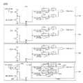
도 2에 도시된 바와 같이, 오류 검출 회로(200)는 스캔 제어 신호 생성부(300) 및 관통 비아 스캔부(500)를 포함할 수 있다.As shown in FIG. 2 , the
스캔 제어 신호 생성부(300)는 클럭 신호(CLK) 및 소스 신호(COUT0)에 따라 스캔 제어 신호들 즉, 업 스캔 신호(UP_SCAN), 다운 스캔 신호(DN_SCAN) 및 래치 신호(LATCH)를 생성할 수 있다.The scan
이때 클럭 신호(CLK) 및 소스 신호(COUT0)는 도 1의 어레이 퓨즈 회로(900)의 붓 업 동작 시 사용될 수 있는 신호들이며, 이들을 이용할 수 있다.In this case, the clock signal CLK and the source signal COUT0 are signals that can be used during the boot-up operation of the
관통 비아 스캔부(500)는 업 스캔 신호(UP_SCAN), 다운 스캔 신호(DN_SCAN) 및 래치 신호(LATCH)에 따라 관통 비아들(TSV)에 대한 스캔을 수행하여 관통 비아들(TSV)의 불량 여부를 정의하는 복수의 불량 판정 신호(FAIL<0:n>)를 생성할 수 있다.The through-
이때 복수의 불량 판정 신호(FAIL<0:n>)는 모든 관통 비아(TSV)의 불량 판정 여부를 정의할 수 있으며, 관통 비아들(TSV)의 수가 n+1개인 경우의 예를 든 것이다.In this case, the plurality of failure determination signals FAIL<0:n> may define whether or not all through-vias TSVs are defective, and the case where the number of through-vias TSV is n+1 is exemplified.
추후 설명에 앞서, 관통 비아 스캔부(500)는 관통 비아들(TSV) 중에서 동일 신호를 전달하기 위한 열(Column) 방향 관통 비아들(TSV)에 대하여 업 스캔 및 다운 스캔을 수행하여 복수의 불량 판정 신호(FAIL<0:n>)를 생성할 수 있다.Prior to a description later, the through-via
도 3 및 도 4에 도시된 바와 같이, 스캔 제어신호 생성부(300)는 복수의 플립플롭(310) 및 제 1 내지 제 9 로직 게이트(321 - 345)를 포함할 수 있다.3 and 4 , the scan
복수의 플립플롭(310)은 클럭 신호(CLK)에 따라 소스 신호(COUT0)를 순차적으로 쉬프트시켜 복수의 쉬프트 신호(COUT1 - COUT7)를 생성할 수 있다.The plurality of flip-
제 1 로직 게이트(321)는 복수의 쉬프트 신호(COUT1 - COUT7) 중에서 COUT3을 반전시켜 출력할 수 있다.The
제 2 로직 게이트(322)는 소스 신호(COUT0)와 제 1 로직 게이트(321)의 출력 신호를 논리곱하여 다운 스캔 신호(DN_SCAN)로서 출력할 수 있다.The
제 3 로직 게이트(331)는 복수의 쉬프트 신호(COUT1 - COUT7) 중에서 COUT6을 반전시켜 출력할 수 있다.The
제 4 로직 게이트(332)는 복수의 쉬프트 신호(COUT1 - COUT7) 중에서 COUT3와 제 3 로직 게이트(331)의 출력 신호를 논리곱하여 업 스캔 신호(UP_SCAN)로서 출력할 수 있다.The
제 5 로직 게이트(341)는 복수의 쉬프트 신호(COUT1 - COUT7) 중에서 COUT2을 반전시켜 출력할 수 있다.The
제 6 로직 게이트(342)는 복수의 쉬프트 신호(COUT1 - COUT7) 중에서 COUT1와 제 5 로직 게이트(341)의 출력 신호를 부정 논리곱하여 출력할 수 있다.The
제 7 로직 게이트(343)는 복수의 쉬프트 신호(COUT1 - COUT7) 중에서 COUT5을 반전시켜 출력할 수 있다.The
제 8 로직 게이트(344)는 복수의 쉬프트 신호(COUT1 - COUT7) 중에서 COUT4와 제 7 로직 게이트(343)의 출력 신호를 부정 논리곱하여 출력할 수 있다.The
제 9 로직 게이트(345)는 제 6 로직 게이트(342)의 출력 신호와 제 8 로직 게이트(344)의 출력 신호를 부정 논리곱하여 래치 신호(LATCH)로서 출력할 수 있다.The
도 4에 도시된 바와 같이, 다운 스캔 신호(DN_SCAN)가 COUT0의 라이징 엣지에서 COUT3의 라이징 엣지에 해당하는 구간 동안 활성화된 후, 업 스캔 신호(UP_SCAN)가 COUT3의 라이징 엣지에서 COUT6의 라이징 엣지에 해당하는 구간 동안 활성화될 수 있다.As shown in FIG. 4 , after the down scan signal DN_SCAN is activated during the period from the rising edge of COUT0 to the rising edge of COUT3, the up scan signal UP_SCAN is applied from the rising edge of COUT3 to the rising edge of COUT6. It can be activated during the corresponding section.
또한 래치 신호(LATCH)는 다운 스캔 신호(DN_SCAN)의 활성화 구간, 그리고 업 스캔 신호(UP_SCAN)의 활성화 구간에 각각 한번씩 활성화될 수 있다.In addition, the latch signal LATCH may be activated once each during an activation period of the down scan signal DN_SCAN and an activation period of the up scan signal UP_SCAN.
도 5에 도시된 바와 같이, 관통 비아 스캔부(500)는 적층된 반도체 칩들(101 ~ 104) 각각에 포함될 수 있다. 이때 도 5는 적층된 반도체 칩들(101 ~ 104)의 관통 비아들(TSV) 중에서 열(Column) 방향으로 동일 선상에 위치한 하나씩의 관통 비아들에 따른 관통 비아 스캔부(500)의 예를 든 것이다.5 , the through-
관통 비아 스캔부(500)는 커런트 소스(Current Source)(510), 커런트 리커(Current Leaker)(520) 및 불량 판정부(530)를 포함할 수 있다.The through-
커런트 소스(510)는 업 스캔 신호(UP_SCAN) 또는 다운 스캔 신호(DN_SCAN)에 따라 전원단에서 관통 비아(TSV)로 전류가 흐르도록 할 수 있으며, 인버터 및 PMOS 트랜지스터를 포함할 수 있다.The
커런트 리커(520)는 업 스캔 신호(UP_SCAN) 또는 다운 스캔 신호(DN_SCAN)에 따라 관통 비아(TSV)에서 접지단으로 전류가 흐르도록 할 수 있으며 NMOS 트랜지스터를 포함할 수 있다.The
불량 판정부(530)는 업 스캔 신호(UP_SCAN)와 다운 스캔 신호(DN_SCAN) 각각에 따른 관통 비아(TSV)의 전압 레벨에 따라 복수의 불량 판정 신호(FAIL<0:n>)를 생성할 수 있다.The
불량 판정부(530)는 제 1 내지 제 7 로직 게이트(531 - 537) 및 제 1 내지 제 2 래치(538, 539)를 포함할 수 있다.The
제 1 로직 게이트(531)는 다운 스캔 신호(DN_SCAN)와 래치 신호(LATCH)를 논리곱하여 출력할 수 있다.The
제 2 로직 게이트(532)는 제 1 로직 게이트(531)의 출력 신호를 반전시켜 출력할 수 있다.The
제 3 로직 게이트(533)는 제 1 로직 게이트(531)의 출력 신호를 비 반전 제어단자에 입력 받고, 제 2 로직 게이트(532)의 출력 신호를 반전 제어단자에 입력받을 수 있다.The
제 3 로직 게이트(533)는 비 반전 제어단자의 레벨이 로직 하이이고, 반전 제어 단자의 레벨이 로직 로우인 경우에만 입력 신호를 통과시킬 수 있다.The
제 1 래치(538)는 제 3 로직 게이트(533)의 출력 신호를 저장할 수 있다.The
제 4 로직 게이트(534)는 업 스캔 신호(UP_SCAN)와 래치 신호(LATCH)를 논리곱하여 출력할 수 있다.The
제 5 로직 게이트(535)는 제 4 로직 게이트(534)의 출력 신호를 반전시켜 출력할 수 있다.The
제 6 로직 게이트(536)는 제 4 로직 게이트(534)의 출력 신호를 비 반전 제어단자에 입력 받고, 제 5 로직 게이트(535)의 출력 신호를 반전 제어단자에 입력받을 수 있다.The
제 6 로직 게이트(536)는 비 반전 제어단자의 레벨이 로직 하이이고, 반전 제어 단자의 레벨이 로직 로우인 경우에만 입력 신호를 통과시킬 수 있다.The
제 2 래치(539)는 제 6 로직 게이트(536)의 출력 신호를 저장할 수 있다.The
제 7 로직 게이트(537)는 제 1 래치(538)에 저장된 신호와 제 2 래치(539)에 저장된 신호를 부정 논리곱하여 복수의 불량 판정 신호(FAIL<0:n>) 중에서 어느 하나로서 출력할 수 있다.The
이때 적층된 반도체 칩들(101 ~ 104) 중에서 최상위의 반도체 칩(104)의 커런트 소스(510)에는 다운 스캔 신호(DN_SCAN)가 입력되고, 커런트 리커(520)에는 업 스캔 신호(UP_SCAN)가 입력될 수 있다.At this time, the down scan signal DN_SCAN is input to the
적층된 반도체 칩들(101 ~ 104) 중에서 최하위의 반도체 칩(101)의 커런트 소스(510)에는 업 스캔 신호(UP_SCAN)가 입력되고, 커런트 리커(520)에는 다운 스캔 신호(DN_SCAN)가 입력될 수 있다.An up scan signal UP_SCAN may be input to the
최상위의 반도체 칩(104)과 최하위의 반도체 칩(101)을 제외한 나머지 반도체 칩들(102, 013)의 커런트 소스(510)와 커런트 리커(520)의 입력단 즉, 인버터의 입력단과 NMOS 트랜지스터의 게이트는 플로팅될 수 있다.The input terminal of the
이때 적층된 반도체 칩들(101 ~ 104)은 적층이 이루어짐에 따라 적층 정보가 반도체 칩 별로 저장될 수 있다.In this case, as the
적층 정보는 해당 반도체 칩의 적층 위치 즉, 최상위, 최하위와 중간을 정의할 수 있는 정보이다.The stacking information is information that can define stacking positions of the corresponding semiconductor chip, that is, the highest, lowest, and middle.
따라서 본 발명의 실시예는 적층 정보를 이용하여 도 5와 같이, 반도체 칩의 위치에 따라 커런트 소스(510)와 커런트 리커(520)에 다운 스캔 신호(DN_SCAN)와 업 스캔 신호(UP_SCAN)를 선택적으로 입력시키거나, 커런트 소스(510)와 커런트 리커(520)를 플로팅시킬 수 있다.Accordingly, according to the embodiment of the present invention, the down scan signal DN_SCAN and the up scan signal UP_SCAN are selectively selected from the
도 4 및 도 5를 참조하여 본 발명의 실시예에 따른 관통 비아 불량 검출 동작을 설명하면 다음과 같다.A through-via defect detection operation according to an embodiment of the present invention will be described with reference to FIGS. 4 and 5 .
먼저, 다운 스캔 신호(DN_SCAN)가 활성화됨에 따라 최상위 반도체 칩(104)의 커런트 소스(510)에서 관통 비아들(TSV)을 통해 최하위 반도체 칩(101)의 커런트 리커(520)로 전류가 흐른다.First, as the down scan signal DN_SCAN is activated, a current flows from the
다운 스캔 신호(DN_SCAN)의 활성화 구간 동안 업 스캔 신호(UP_SCAN)는 비 활성화되므로 최상위 반도체 칩(104)의 커런트 리커(520) 및 최하위 반도체 칩(101)의 커런트 소스(510)는 비 활성화된다.Since the up scan signal UP_SCAN is inactivated during the activation period of the down scan signal DN_SCAN, the
적층된 반도체 칩들(101 ~ 104) 각각의 불량 판정부(530)는 다운 스캔 신호(DN_SCAN)가 활성화된 상태에서 래치 신호(LATCH)가 활성화됨에 따라, 자신과 연결된 관통 비아(TSV)를 통해 흐르는 전류에 따른 전압 레벨을 다운 스캔의 결과 값으로서 저장한다.The
이어서, 업 스캔 신호(UP_SCAN)가 활성화됨에 따라 최하위 반도체 칩(101)의 커런트 소스(510)에서 관통 비아들(TSV)을 통해 최상위 반도체 칩(104)의 커런트 리커(520)로 전류가 흐른다.Subsequently, as the up-scan signal UP_SCAN is activated, a current flows from the
업 스캔 신호(UP_SCAN)의 활성화 구간 동안 다운 스캔 신호(DN_SCAN)는 비 활성화되므로 최하위 반도체 칩(101)의 커런트 리커(520) 및 최상위 반도체 칩(104)의 커런트 소스(510)는 비 활성화된다.Since the down scan signal DN_SCAN is inactivated during the activation period of the up scan signal UP_SCAN, the
적층된 반도체 칩들(101 ~ 104) 각각의 불량 판정부(530)는 업 스캔 신호(UP_SCAN)가 활성화된 상태에서 래치 신호(LATCH)가 활성화됨에 따라, 자신과 연결된 관통 비아(TSV)를 통해 흐르는 전류에 따른 전압 레벨을 업 스캔의 결과 값으로서 저장한다.The
적층된 반도체 칩들(101 ~ 104) 각각의 불량 판정부(530)는 기 저장된 다운 스캔의 결과 값과 업 스캔의 결과 값이 모두 해당 관통 비아(TSV)의 정상을 정의하는 값(예를 들어, 하이 레벨)이면 불량 판정 신호(FAIL<0:n>)를 비 활성화(로우 레벨)시킬 수 있다.The
한편, 기 저장된 다운 스캔의 결과 값과 업 스캔의 결과 값 중에서 어느 하나라도 해당 관통 비아(TSV)의 불량을 정의하는 값(예를 들어, 로우 레벨)이면 불량 판정 신호(FAIL<0:n>)를 활성화(하이 레벨)시킬 수 있다.On the other hand, if any one of the pre-stored down-scan result value and up-scan result value is a value (eg, low level) defining the failure of the corresponding through-via TSV, the failure determination signal (FAIL<0:n>) ) can be activated (high level).
도 6은 관통 비아들(TSV) 중에서 일부 TSV<m:m+2>에 따른 리페어 회로(700)를 도시한 것이다.FIG. 6 illustrates a
도 6에 도시된 바와 같이, 리페어 회로(700)는 관통 비아들(TSV<m:m+2>) 각각과 연결된 제 1 입/출력 드라이버들(710 - 712) 및 제 2 입/출력 드라이버들(720 - 722)를 포함할 수 있다.As shown in FIG. 6 , the
제 1 입/출력 드라이버들(710 - 712)은 서로 동일하게 구성될 수 있으며, 제 2 입/출력 드라이버들(720 - 722) 또한 서로 동일하게 구성될 수 있다.The first input/
제 1 입/출력 드라이버들(710 - 712) 및 제 2 입/출력 드라이버들(720 - 722)은 불량 판정 신호(FAIL<0:n>)에 따라 불량 판정된 관통 비아(TSV)와 연결된 입/출력 경로를 정상 관통 비아(TSV)와 연결된 입/출력 경로로 전환하도록 구성될 수 있다.The first input/output drivers 710 - 712 and the second input/output drivers 720 - 722 are input/output connected to the through-via TSV determined to be defective according to the failure determination signal FAIL<0:n>. It can be configured to convert the /output path to an input/output path connected to a normal through via (TSV).
제 1 입/출력 드라이버(710)는 제 1 신호 입/출력 라인들(GIO) 중에서 어느 하나의 제 1 신호 입/출력 라인(GIO<m>)과 관통 비아들(TSV) 중에서 어느 하나의 관통 비아(TSV<m>) 사이에 연결될 수 있다.The first input/
제 1 입/출력 드라이버(710)는 입력 드라이버(RX) 및 출력 드라이버(TX)를 포함할 수 있다.The first input/
제 1 입/출력 드라이버(710)의 입력 드라이버(RX)는 불량 판정 신호(FAIL<m>)에 따라 제 1 신호 입/출력 라인(GIO<m>) 또는 이전 순번의 제 1 신호 입/출력 라인(GIO<m-1>)을 통해 전송된 신호를 관통 비아(TSV<m>)에 드라이빙할 수 있다.The input driver RX of the first input/
제 1 입/출력 드라이버(710)의 출력 드라이버(TX)는 불량 판정 신호(FAIL<m>)에 따라 관통 비아들(TSV<m>) 또는 다음 순번의 관통 비아(TSV<m+1>)를 통해 전송된 신호를 제 1 신호 입/출력 라인(GIO<m>)에 드라이빙할 수 있다.The output driver TX of the first input/
제 2 입/출력 드라이버(720)는 관통 비아(TSV<m>)와 제 2 신호 입/출력 라인(MIO<m>) 사이에 연결될 수 있다.The second input/
제 2 입/출력 드라이버(720)는 입력 드라이버(RX) 및 출력 드라이버(TX)를 포함할 수 있다.The second input/
제 2 입/출력 드라이버(720)의 입력 드라이버(RX)는 불량 판정 신호(FAIL<m>)에 따라 제 2 신호 입/출력 라인(MIO<m>) 또는 이전 순번의 제 2 신호 입/출력 라인(MIO<m-1>)을 통해 전송된 신호를 관통 비아(TSV<m>)에 드라이빙할 수 있다.The input driver RX of the second input/
제 2 입/출력 드라이버(720)의 출력 드라이버(TX)는 불량 판정 신호(FAIL<m>)에 따라 관통 비아(TSV<m>) 또는 다음 순번의 관통 비아(TSV<m+1>)를 통해 전송된 신호를 제 2 신호 입/출력 라인(MIO<m>)에 드라이빙할 수 있다.The output driver TX of the second input/
도 7을 참조하면, 본 발명의 실시예에 따른 관통 비아(TSV) 리페어 동작을 설명하면 다음과 같다.Referring to FIG. 7 , a through-via (TSV) repair operation according to an embodiment of the present invention will be described as follows.
예를 들어, 관통 비아들(TSV) 중에서 관통 비아(TSV<m+1>)가 불량인 경우의 리페어 동작을 설명하기로 한다.For example, a repair operation in the case where the through-via TSV<m+1> among the through-vias TSV is defective will be described.
관통 비아(TSV<m+1>)가 불량이므로 도 4 및 도 5를 참조하여 이미 설명한 관통 비아 불량 검출 동작을 통해 불량 판정 신호들(FAIL) 중에서 불량 판정 신호(FAIL<m+1>)가 활성화된 상태이며, 불량 판정 신호(FAIL<m+2>)를 포함한 그 다음 순번들에 해당하는 불량 판정 신호들 또한 활성화된다.Since the through-via TSV<m+1> is defective, the failure determination signal FAIL<m+1> is In an activated state, the failure determination signals corresponding to the next sequence including the failure determination signal FAIL<m+2> are also activated.
이때 본 발명의 실시예에 따른 관통 비아(TSV) 리페어 동작은 불량이 발생한 관통 비아(TSV)와 연결된 입/출력 경로를 쉬프트시키는 방식 즉, 우측(도 7 기준)의 정상 관통 비아(TSV)에 연결하는 방식으로 이루어질 수 있다.At this time, the TSV repair operation according to the embodiment of the present invention is a method of shifting the input/output path connected to the defective TSV, that is, to the normal TSV on the right side (based on FIG. 7 ). This can be done by connecting
따라서 불량 판정 신호(FAIL<m+1>)가 활성화되면 불량 판정 신호(FAIL<m+2>)를 포함한 불량 판정 신호(FAIL<m+1>)의 다음 순번들에 해당하는 불량 판정 신호들 또한 활성화시킬 수 있다.Therefore, when the failure determination signal FAIL<m+1> is activated, the failure determination signals corresponding to the following sequence numbers of the failure determination signal FAIL<m+1> including the failure determination signal FAIL<m+2> It can also be activated.
불량 판정 신호(FAIL<m>)가 비 활성화 상태이므로 제 1 신호 입/출력 라인(GIO<m>)과 제 2 신호 입/출력 라인(MIO<m>) 사이의 신호 입/출력이 제 1 입/출력 드라이버(710)와 제 2 입/출력 드라이버(720)에 의해 관통 비아(TSV<m>)를 통해 이루어질 수 있다.Since the failure determination signal (FAIL<m>) is in an inactive state, the signal input/output between the first signal input/output line (GIO<m>) and the second signal input/output line (MIO<m>) is The input/
불량 판정 신호(FAIL<m+1>)가 활성화 상태이므로 제 1 신호 입/출력 라인(GIO<m+1>)과 제 2 신호 입/출력 라인(MIO<m+1>) 사이의 신호 입/출력이 제 1 입/출력 드라이버(711)와 제 2 입/출력 드라이버(721)에 의해 관통 비아(TSV<m+2>)를 통해 이루어질 수 있다.Since the failure determination signal (FAIL<m+1>) is active, the signal input between the first signal input/output line (GIO<m+1>) and the second signal input/output line (MIO<m+1>) is /output may be performed through the through via TSV<m+2> by the first input/
상술한 바와 같이, 제 1 신호 입/출력 라인들(GIO)과 제 2 신호 입/출력 라인들(MIO) 사이의 신호 입/출력이 불량이 발생한 관통 비아(TSV<m+1>)를 기준으로 우측의 관통 비아(TSV<m+2>)로 한 칸씩 쉬프트됨으로써 리페어 동작이 이루어질 수 있다.As described above, the signal input/output between the first signal input/output lines GIO and the second signal input/output lines MIO is based on the defective through-via TSV<m+1>. The repair operation can be performed by shifting one by one to the right through via (TSV<m+2>).
도 8에 도시된 바와 같이, 본 발명의 다른 실시예에 따른 반도체 장치(1000)는 적층된 복수의 반도체 칩(101 ~ 104)을 포함할 수 있다.As shown in FIG. 8 , a
적층된 반도체 칩들(101 ~ 104)은 각각 오류 검출 회로(201) 및 리페어 회로(700)를 포함할 수 있다.Each of the stacked
오류 검출 회로(201)는 해당 반도체 칩의 관통 비아들(TSV)의 불량을 검출하여 불량 판정 신호들(FAIL<0:n>)을 생성할 수 있다.The
오류 검출 회로(201)는 다운 스캔의 결과 값을 초기화한 후 관통 비아들(TSV) 중에서 열(Column) 방향의 관통 비아들에 대하여 하위 방향으로 신호를 전달하는 다운 스캔을 수행하고, 업 스캔의 결과 값을 초기화한 후 열 방향의 관통 비아들(TSV)에 대하여 상위 방향으로 신호를 전달하는 업 스캔을 수행하며, 다운 스캔의 결과 값과 상기 업 스캔의 결과 값에 따라 관통 비아들(TSV)의 불량 여부를 판정하여 불량 판정 신호들(FAIL<0:n>)을 생성할 수 있다.The
리페어 회로(700)는 오류 검출 신호(FAIL<0:n>)에 따라 불량 판정된 관통 비아(TSV)를 정상 상태의 관통 비아(TSV)로 대체할 수 있다.The
리페어 회로(700)의 구성 및 동작은 이미 도 6 및 7을 참조하여 설명한 것과 같으므로 이하에서의 설명은 생략하기로 한다.The configuration and operation of the
적층된 반도체 칩들(101 ~ 104)은 각각 어레이 퓨즈 회로(900)를 더 포함할 수 있다.Each of the stacked
어레이 퓨즈 회로(900)는 반도체 칩에 포함된 메모리 영역의 메모리 셀들 중에서 불량이 발생한 메모리 셀의 컬럼/로우 리페어 동작에 관련된 정보를 입/출력하기 위한 어레이 퓨즈 및 로직 회로 등을 포함할 수 있다.The
도 9에 도시된 바와 같이, 오류 검출 회로(201)는 스캔 제어 신호 생성부(301) 및 관통 비아 스캔부(501)를 포함할 수 있다.As shown in FIG. 9 , the
스캔 제어 신호 생성부(301)는 붓업 카운트 신호(BU_CNT)에 따라 스캔 제어 신호들 즉, 제 1 프리셋 신호(PRESET_DN), 다운 스캔 신호(DN_SCAN), 제 2 프리셋 신호(PRESET_UP) 및 업 스캔 신호(UP_SCAN)를 생성할 수 있다.The scan
이때 붓업 카운트 신호(BU_CNT)는 도 8의 어레이 퓨즈 회로(900)의 붓 업 동작 시 사용되는 신호일 수 있다.In this case, the boot-up count signal BU_CNT may be a signal used during the boot-up operation of the
관통 비아 스캔부(501)는 제 1 프리셋 신호(PRESET_DN), 다운 스캔 신호(DN_SCAN), 제 2 프리셋 신호(PRESET_UP) 및 업 스캔 신호(UP_SCAN)에 따라 다운 스캔의 결과 값 초기화, 업 스캔의 결과 값 초기화, 다운 스캔 및 업 스캔을 수행하고, 다운 스캔의 결과 값과 업 스캔의 결과 값에 따라 관통 비아들의 불량 여부를 정의하는 불량 판정 신호들(FAIL<0:n>)을 생성할 수 있다.The through-via
이때 복수의 불량 판정 신호(FAIL<0:n>)는 모든 관통 비아(TSV)의 불량 판정 여부를 정의할 수 있으며, 관통 비아들(TSV)의 수가 n+1개인 경우의 예를 든 것이다.In this case, the plurality of failure determination signals FAIL<0:n> may define whether or not all through-vias TSVs are defective, and the case where the number of through-vias TSV is n+1 is exemplified.
추후 설명에 앞서, 관통 비아 스캔부(500)는 관통 비아들(TSV) 중에서 동일 신호를 전달하기 위한 열(Column) 방향 관통 비아들(TSV)에 대하여 업 스캔 및 다운 스캔을 수행하여 복수의 불량 판정 신호(FAIL<0:n>)를 생성할 수 있다.Prior to a description later, the through-via
도 10에 도시된 바와 같이, 스캔 제어신호 생성부(301)는 플립플롭 어레이(350) 및 카운터(360)를 포함할 수 있다.As shown in FIG. 10 , the scan
플립플롭 어레이(350)의 플립플롭들(351)은 붓업 카운트 신호(BU_CNT)에 따라 스캔 시작 신호(SCAN_START)를 순차적으로 쉬프트시켜 스캔 제어 신호들 즉, 제 1 프리셋 신호(PRESET_DN), 다운 스캔 신호(DN_SCAN), 제 2 프리셋 신호(PRESET_UP) 및 업 스캔 신호(UP_SCAN)를 생성할 수 있다.The flip-
카운터(360)는 붓업 카운트 신호(BU_CNT)를 카운트하여 기 설정된 타이밍에 스캔 시작 신호(SCAN_START)를 활성화시킬 수 있다.The
도 11에 도시된 바와 같이, 스캔 시작 신호(SCAN_START)가 활성화되고 다음 타이밍의 붓업 카운트 신호(BU_CNT)에 따라 제 1 프리셋 신호(PRESET_DN)가 활성화되고, 붓업 카운트 신호(BU_CNT)의 펄스를 기준으로 정해진 간격을 두고 다운 스캔 신호(DN_SCAN), 제 2 프리셋 신호(PRESET_UP) 및 업 스캔 신호(UP_SCAN)가 순차적으로 활성화될 수 있다.11 , the scan start signal SCAN_START is activated and the first preset signal PRESET_DN is activated according to the boot-up count signal BU_CNT at the next timing, and based on the pulse of the boot-up count signal BU_CNT. The down scan signal DN_SCAN, the second preset signal PRESET_UP, and the up scan signal UP_SCAN may be sequentially activated at predetermined intervals.
도 11은 도 10의 회로 구성을 기준으로 한 것일 뿐, 카운터(360)의 내부 설정 값을 조정하거나, 플립플롭들(351) 중에서 출력 신호를 인출하는 플립플롭(351)을 조정함에 따라 원하는 타이밍 및 원하는 간격을 두고 제 1 프리셋 신호(PRESET_DN), 다운 스캔 신호(DN_SCAN), 제 2 프리셋 신호(PRESET_UP) 및 업 스캔 신호(UP_SCAN)가 활성화되도록 할 수 있다.FIG. 11 is only based on the circuit configuration of FIG. 10 , and a desired timing by adjusting the internal setting value of the
도 12에 도시된 바와 같이, 관통 비아 스캔부(501)는 적층된 반도체 칩들(101 ~ 104) 각각에 포함될 수 있다. 이때 도 12는 적층된 반도체 칩들(101 ~ 104)의 관통 비아들(TSV) 중에서 열(Column) 방향으로 동일 선상에 위치한 하나씩의 관통 비아들에 따른 관통 비아 스캔부(501)의 예를 든 것이다.12 , the through-via
관통 비아 스캔부(501)는 커런트 소스(Current Source)(510), 커런트 리커(Current Leaker)(520) 및 불량 판정부(540)를 포함할 수 있다.The through-via
커런트 소스(510) 및 커런트 리커(520)는 도 5와 같이 구성할 수 있다.The
불량 판정부(540)는 다운 스캔의 결과 값을 제 1 프리셋 신호(PRESET_DN)에 따라 초기화하고 다운 스캔 신호(DN_SCAN)에 따라 다운 스캔의 결과 값을 저장할 수 있다.The
불량 판정부(540)는 업 스캔의 결과 값을 제 2 프리셋 신호(PRESET_UP)에 따라 초기화하고 업 스캔 신호(UP_SCAN)에 따라 업 스캔의 결과 값을 저장할 수 있다.The
불량 판정부(540)는 다운 스캔의 결과 값과 업 스캔의 결과 값을 조합하여 복수의 불량 판정 신호(FAIL<0:n>)를 생성할 수 있다.The
불량 판정부(540)는 업 스캔 신호(UP_SCAN)와 다운 스캔 신호(DN_SCAN) 각각에 따른 관통 비아(TSV)의 전압 레벨을 다운 스캔의 결과 값과 업 스캔의 결과 값으로서 저장할 수 있다.The
불량 판정부(540)는 제 1 패스 게이트(PG1)(541), 제 2 패스 게이트(PG2)(542), 제 1 래치(543), 제 2 래치(544), 낸드 게이트(545), 제 1 트랜지스터(546) 및 제 2 트랜지스터(547)를 포함할 수 있다.The
제 1 패스 게이트(541)는 다운 스캔 신호(DN_SCAN)가 하이 레벨인 경우 입력 신호 즉, 관통 전극(TSV)의 전압 레벨을 제 1 래치(543)에 저장할 수 있다.The
제 2 패스 게이트(542)는 업 스캔 신호(UP_SCAN)가 하이 레벨인 경우 입력 신호 즉, 관통 전극(TSV)의 전압 레벨을 제 2 래치(544)에 저장할 수 있다.The
낸드 게이트(545)는 제 1 래치(543)에 저장된 신호 레벨과 제 2 래치(544)에 저장된 신호 레벨이 모두 하이 레벨인 경우 불량 판정 신호(FAIL<0:n>)를 로우 레벨로 출력하고, 둘 중에서 하나라도 로우 레벨인 경우 불량 판정 신호(FAIL<0:n>)를 하이 레벨로 출력한다.When the signal level stored in the
제 1 트랜지스터(546)는 제 1 프리셋 신호(PRESET_DN)가 하이 레벨인 경우, 다운 스캔의 결과 값 즉, 제 1 래치(543)에 저장된 신호 레벨을 하이 레벨로 초기화시킨다.When the first preset signal PRESET_DN is at a high level, the
제 2 트랜지스터(547)는 제 2 프리셋 신호(PRESET_UP)가 하이 레벨인 경우, 업 스캔의 결과 값 즉, 제 2 래치(544)에 저장된 신호 레벨을 하이 레벨로 초기화시킨다.When the second preset signal PRESET_UP is at the high level, the
제 1 래치(543)에 저장된 신호 레벨과 제 2 래치(544)에 저장된 신호 레벨이 모두 하이 레벨이므로 불량 판정 신호(FAIL<0:n>)가 로우 레벨로 초기화될 수 있다.Since both the signal level stored in the
이때 적층된 반도체 칩들(101 ~ 104) 중에서 최상위의 반도체 칩(104)의 커런트 소스(510)에는 다운 스캔 신호(DN_SCAN)가 입력되고, 커런트 리커(520)에는 업 스캔 신호(UP_SCAN)가 입력될 수 있다.At this time, the down scan signal DN_SCAN is input to the
적층된 반도체 칩들(101 ~ 104) 중에서 최하위의 반도체 칩(101)의 커런트 소스(510)에는 업 스캔 신호(UP_SCAN)가 입력되고, 커런트 리커(520)에는 다운 스캔 신호(DN_SCAN)가 입력될 수 있다.An up scan signal UP_SCAN may be input to the
최상위의 반도체 칩(104)과 최하위의 반도체 칩(101)을 제외한 나머지 반도체 칩들(102, 013)의 커런트 소스(510)와 커런트 리커(520)의 입력단 즉, 인버터의 입력단과 NMOS 트랜지스터의 게이트는 플로팅될 수 있다.The input terminal of the
이때 적층된 반도체 칩들(101 ~ 104)은 적층이 이루어짐에 따라 적층 정보가 반도체 칩 별로 저장될 수 있다.In this case, as the
적층 정보는 해당 반도체 칩의 적층 위치 즉, 최상위, 최하위와 중간을 정의할 수 있는 정보이다.The stacking information is information that can define stacking positions of the corresponding semiconductor chip, that is, the highest, lowest, and middle.
따라서 본 발명의 다른 실시예는 적층 정보를 이용하여 도 12와 같이, 반도체 칩의 위치에 따라 커런트 소스(510)와 커런트 리커(520)에 다운 스캔 신호(DN_SCAN)와 업 스캔 신호(UP_SCAN)를 선택적으로 입력시키거나, 커런트 소스(510)와 커런트 리커(520)를 플로팅시킬 수 있다.Accordingly, according to another embodiment of the present invention, a down scan signal DN_SCAN and an up scan signal UP_SCAN are applied to the
도 11 및 도 12를 참조하여 본 발명의 실시예에 따른 관통 비아 불량 검출 동작을 설명하면 다음과 같다.A through-via defect detection operation according to an embodiment of the present invention will be described with reference to FIGS. 11 and 12 .
반도체 장치의 파워 업 이후에 여러가지 이유로 붓 업 동작 이전에 스캔 동작에 관련된 비정상적인 신호(Abnormal Signal)이 생성될 수 있다.After power-up of the semiconductor device, an abnormal signal related to the scan operation may be generated before the boot-up operation for various reasons.
이후, 붓 업 동작이 수행되고 그에 따라 붓업 카운트 신호(BU_CNT)가 활성화될 수 있다.Thereafter, the boot-up operation is performed, and accordingly, the boot-up count signal BU_CNT may be activated.
붓업 카운트 신호(BU_CNT)의 펄스 들이 생성되고 정해진 타이밍 이후에 스캔 시작 신호(SCAN_START)가 활성화되고, 스캔 시작 신호(SCAN_START)에 따라 제 1 프리셋 신호(PRESET_DN), 다운 스캔 신호(DN_SCAN), 제 2 프리셋 신호(PRESET_UP) 및 업 스캔 신호(UP_SCAN)가 순차적으로 활성화될 수 있다.Pulses of the boot-up count signal BU_CNT are generated and the scan start signal SCAN_START is activated after a predetermined timing, and according to the scan start signal SCAN_START, the first preset signal PRESET_DN, the down scan signal DN_SCAN, and the second The preset signal PRESET_UP and the up scan signal UP_SCAN may be sequentially activated.
제 1 프리셋 신호(PRESET_DN)에 따라 다운 스캔의 결과 값이 하이 레벨로 초기화된다.A result value of the down scan is initialized to a high level according to the first preset signal PRESET_DN.
다운 스캔 신호(DN_SCAN)가 활성화됨에 따라 최상위 반도체 칩(104)의 커런트 소스(510)에서 관통 비아들(TSV)을 통해 최하위 반도체 칩(101)의 커런트 리커(520)로 전류가 흐른다.As the down scan signal DN_SCAN is activated, a current flows from the
다운 스캔 신호(DN_SCAN)의 활성화 구간 동안 업 스캔 신호(UP_SCAN)는 비 활성화되므로 최상위 반도체 칩(104)의 커런트 리커(520) 및 최하위 반도체 칩(101)의 커런트 소스(510)는 비 활성화된다.Since the up scan signal UP_SCAN is inactivated during the activation period of the down scan signal DN_SCAN, the
적층된 반도체 칩들(101 ~ 104) 각각의 불량 판정부(540)는 다운 스캔 신호(DN_SCAN)가 활성화됨에 따라, 자신과 연결된 관통 비아(TSV)를 통해 흐르는 전류에 따른 전압 레벨을 다운 스캔의 결과 값으로서 저장한다.As the down scan signal DN_SCAN is activated, the
제 2 프리셋 신호(PRESET_UP)에 따라 업 스캔의 결과 값이 하이 레벨로 초기화된다.According to the second preset signal PRESET_UP, the up-scan result value is initialized to a high level.
이어서, 업 스캔 신호(UP_SCAN)가 활성화됨에 따라 최하위 반도체 칩(101)의 커런트 소스(510)에서 관통 비아들(TSV)을 통해 최상위 반도체 칩(104)의 커런트 리커(520)로 전류가 흐른다.Subsequently, as the up-scan signal UP_SCAN is activated, a current flows from the
업 스캔 신호(UP_SCAN)의 활성화 구간 동안 다운 스캔 신호(DN_SCAN)는 비 활성화되므로 최하위 반도체 칩(101)의 커런트 리커(520) 및 최상위 반도체 칩(104)의 커런트 소스(510)는 비 활성화된다.Since the down scan signal DN_SCAN is inactivated during the activation period of the up scan signal UP_SCAN, the
적층된 반도체 칩들(101 ~ 104) 각각의 불량 판정부(540)는 업 스캔 신호(UP_SCAN)가 활성화됨에 따라, 자신과 연결된 관통 비아(TSV)를 통해 흐르는 전류에 따른 전압 레벨을 업 스캔의 결과 값으로서 저장한다.The
적층된 반도체 칩들(101 ~ 104) 각각의 불량 판정부(540)는 기 저장된 다운 스캔의 결과 값과 업 스캔의 결과 값이 모두 해당 관통 비아(TSV)의 정상을 정의하는 하이 레벨이면 불량 판정 신호(FAIL<0:n>)를 로우 레벨로 출력할 수 있다.The
한편, 기 저장된 다운 스캔의 결과 값과 업 스캔의 결과 값 중에서 어느 하나라도 해당 관통 비아(TSV)의 불량을 정의하는 로우 레벨이면 불량 판정 신호(FAIL<0:n>)를 하이 레벨로 출력할 수 있다.On the other hand, if any one of the pre-stored down-scan result value and up-scan result value is a low level defining the failure of the corresponding through-via TSV, the failure determination signal FAIL<0:n> is output at a high level. can
이와 같이, 본 발명이 속하는 기술분야의 당업자는 본 발명이 그 기술적 사상이나 필수적 특징을 변경하지 않고서 다른 구체적인 형태로 실시될 수 있다는 것을 이해할 수 있을 것이다. 그러므로 이상에서 기술한 실시예들은 모든 면에서 예시적인 것이며 한정적인 것이 아닌 것으로서 이해해야만 한다. 본 발명의 범위는 상기 상세한 설명보다는 후술하는 특허청구범위에 의하여 나타내어지며, 특허청구범위의 의미 및 범위 그리고 그 등가개념으로부터 도출되는 모든 변경 또는 변형된 형태가 본 발명의 범위에 포함되는 것으로 해석되어야 한다.As such, those skilled in the art to which the present invention pertains will understand that the present invention may be embodied in other specific forms without changing the technical spirit or essential characteristics thereof. Therefore, it should be understood that the embodiments described above are illustrative in all respects and not restrictive. The scope of the present invention is indicated by the following claims rather than the above detailed description, and all changes or modifications derived from the meaning and scope of the claims and their equivalent concepts should be interpreted as being included in the scope of the present invention. do.
Claims (27)
Translated fromKorean상기 적층된 복수의 반도체 칩은
상기 관통 비아들 중에서 열(Column) 방향의 관통 비아들에 대하여 하위 방향으로 신호를 전달하는 다운 스캔 및 상위 방향으로 신호를 전달하는 업 스캔을 수행하며, 상기 다운 스캔의 결과 값과 상기 업 스캔의 결과 값에 따라 상기 관통 비아들의 불량 여부를 판정하도록 구성된 오류 검출 회로를 포함하는 적층형 반도체 장치.A plurality of semiconductor chips stacked so as to transmit a signal through the through vias,
The plurality of stacked semiconductor chips is
Down-scan for transmitting a signal in a lower direction and an up-scan for transmitting a signal in an upper direction are performed on through-vias in a column direction among the through-vias, and the result value of the down-scan and the up-scan and an error detection circuit configured to determine whether the through vias are defective according to a result value.
상기 오류 검출 회로는
상기 열(Column) 방향의 관통 비아들에 대하여 하위 방향으로 전류를 흘려 상기 다운 스캔을 수행하고, 상위 방향으로 전류를 흘려 상기 업 스캔을 수행하도록 구성되는 적층형 반도체 장치.The method of claim 1,
The error detection circuit is
and to perform the down scan by flowing a current in a lower direction with respect to the through vias in the column direction, and to perform the up scan by flowing a current in an upper direction.
상기 오류 검출 회로는
소스 신호에 따라 스캔 제어 신호들을 생성하도록 구성된 스캔 제어신호 생성부, 및
상기 스캔 제어신호들에 따라 상기 다운 스캔 및 상기 업 스캔을 수행하여 상기 관통 비아들의 불량 여부를 정의하는 불량 판정 신호를 생성하도록 구성된 관통 비아 스캔부를 포함하는 적층형 반도체 장치.The method of claim 1,
The error detection circuit is
a scan control signal generator configured to generate scan control signals according to the source signal, and
and a through-via scan unit configured to perform the down-scan and the up-scan according to the scan control signals to generate a failure determination signal defining whether the through-vias are defective.
상기 복수의 반도체 칩은
불량 판정된 메모리 셀의 정보를 저장하기 위한 어레이 퓨즈 회로를 더 포함하며,
상기 어레이 퓨즈 회로의 붓 업(Boot-up) 동작 시 사용되는 신호를 상기 소스 신호로서 사용하는 적층형 반도체 장치.4. The method of claim 3,
The plurality of semiconductor chips
Further comprising an array fuse circuit for storing information of the memory cell determined to be defective,
A multilayer semiconductor device using a signal used in a boot-up operation of the array fuse circuit as the source signal.
상기 스캔 제어신호 생성부는
클럭 신호에 따라 상기 소스 신호를 순차적으로 쉬프트시켜 복수의 쉬프트 신호를 생성하고,
상기 복수의 쉬프트 신호를 설정 단위로 조합하여 상기 스캔 제어신호들을 생성하도록 구성되는 적층형 반도체 장치.4. The method of claim 3,
The scan control signal generator
generating a plurality of shift signals by sequentially shifting the source signal according to a clock signal;
and generate the scan control signals by combining the plurality of shift signals in a set unit.
상기 관통 비아 스캔부는
다운 스캔 신호 또는 업 스캔 신호에 따라 전원단에서 관통 비아로 전류가 흐르도록 하는 커런트 소스,
상기 업 스캔 신호 또는 상기 다운 스캔 신호에 따라 상기 관통 비아에서 접지단으로 전류가 흐르도록 하는 커런트 리커, 및
상기 업 스캔 신호와 상기 다운 스캔 신호 각각에 따른 상기 관통 비아의 전압 레벨에 따라 상기 불량 판정 신호를 생성하도록 구성된 불량 판정부를 포함하는 적층형 반도체 장치.4. The method of claim 3,
The through-via scanning unit
a current source that allows current to flow from the power stage to the through via according to the down scan signal or the up scan signal;
a current leaker for allowing a current to flow from the through-via to a ground terminal according to the up-scan signal or the down-scan signal; and
and a failure determination unit configured to generate the failure determination signal according to a voltage level of the through via according to each of the up-scan signal and the down-scan signal.
상기 불량 판정부는
상기 다운 스캔 신호와 래치 신호에 따라 상기 다운 스캔의 결과 값을 저장하고, 상기 업 스캔 신호와 상기 래치 신호에 따라 상기 업 스캔의 결과 값을 저장하며, 상기 다운 스캔의 결과 값과 상기 업 스캔의 결과 값을 조합하여 상기 불량 판정 신호를 생성하도록 구성되는 적층형 반도체 장치.7. The method of claim 6,
The bad judgment unit
storing a result value of the down scan according to the down scan signal and a latch signal, storing a result value of the up scan according to the up scan signal and the latch signal, and storing the result value of the down scan and the up scan and combine result values to generate the failure determination signal.
상기 복수의 반도체 칩 각각은 자신의 적층 위치를 정의하는 적층 정보가 저장되며,
상기 적층 정보에 따라 상기 커런트 소스에 상기 업 스캔 신호 또는 상기 다운 스캔 신호를 선택적으로 제공하도록 구성되는 적층형 반도체 장치.7. The method of claim 6,
Each of the plurality of semiconductor chips stores stacking information defining its stacking position,
and selectively providing the up-scan signal or the down-scan signal to the current source according to the stacking information.
상기 복수의 반도체 칩 각각은 자신의 적층 위치를 정의하는 적층 정보가 저장되며,
상기 적층 정보에 따라 상기 복수의 반도체 칩 중에서 최상위 반도체 칩과 최하위 반도체 칩을 제외한 나머지 반도체 칩들의 커런트 소스를 플로팅시키도록 구성되는 적층형 반도체 장치.7. The method of claim 6,
Each of the plurality of semiconductor chips stores stacking information defining its stacking position,
and float current sources of the remaining semiconductor chips except for the highest semiconductor chip and the lowest semiconductor chip among the plurality of semiconductor chips according to the stacking information.
상기 오류 검출 회로는
상기 복수의 반도체 칩 중에서 최상위 반도체 칩의 관통 비아를 통해 최하위 반도체 칩의 관통 비아로 전류를 흘려 상기 다운 스캔을 수행하고, 상기 최하위 반도체 칩의 관통 비아에서 상기 최상위 반도체 칩으로 관통 비아로 전류를 흘려 상기 업 스캔을 수행하도록 구성되는 적층형 반도체 장치.The method of claim 1,
The error detection circuit is
The down-scan is performed by flowing a current through a through-via of the uppermost semiconductor chip among the plurality of semiconductor chips to a through-via of the lowermost semiconductor chip, and flowing a current from the through-via of the lowermost semiconductor chip to the through-via of the uppermost semiconductor chip A stacked-type semiconductor device configured to perform the up-scan.
상기 복수의 반도체 칩 중에서 최상위 반도체 칩의 관통 비아를 통해 최하위 반도체 칩의 관통 비아로 전류를 흘려 다운 스캔을 수행하고, 상기 최하위 반도체 칩의 관통 비아에서 상기 최상위 반도체 칩으로 관통 비아로 전류를 흘려 업 스캔을 수행하며, 상기 다운 스캔의 결과 값과 상기 업 스캔의 결과 값에 따라 상기 관통 비아들의 불량 여부를 판정하도록 구성된 오류 검출 회로; 및
상기 오류 검출 회로에 의해 불량 판정된 관통 비아와 연결된 입/출력 경로를 정상 관통 비아와 연결된 입/출력 경로로 전환하도록 구성된 리페어 회로를 포함하는 적층형 반도체 장치.It includes a plurality of semiconductor chips stacked so as to transmit a signal through the through-vias,
A down scan is performed by flowing a current through a through-via of the uppermost semiconductor chip among the plurality of semiconductor chips to a through-via of the lowermost semiconductor chip, and a current flows from the through-via of the lowermost semiconductor chip to the through-via of the uppermost semiconductor chip. an error detection circuit configured to perform a scan and to determine whether the through-vias are defective according to a result value of the down scan and a result value of the up scan; and
and a repair circuit configured to convert an input/output path connected to a through-via determined as defective by the error detection circuit to an input/output path connected to a normal through-via.
상기 오류 검출 회로는
소스 신호에 따라 스캔 제어 신호들을 생성하도록 구성된 스캔 제어신호 생성부, 및
상기 스캔 제어신호들에 따라 상기 다운 스캔 및 상기 업 스캔을 수행하여 상기 관통 비아들의 불량 여부를 정의하는 불량 판정 신호를 생성하도록 구성된 관통 비아 스캔부를 포함하는 적층형 반도체 장치.12. The method of claim 11,
The error detection circuit is
a scan control signal generator configured to generate scan control signals according to the source signal, and
and a through-via scan unit configured to perform the down-scan and the up-scan according to the scan control signals to generate a failure determination signal defining whether the through-vias are defective.
상기 복수의 반도체 칩은
불량 판정된 메모리 셀의 정보를 저장하기 위한 어레이 퓨즈 회로를 더 포함하며,
상기 어레이 퓨즈 회로의 붓 업(Boot-up) 동작 시 사용되는 신호를 상기 소스 신호로서 사용하는 적층형 반도체 장치.13. The method of claim 12,
The plurality of semiconductor chips
Further comprising an array fuse circuit for storing information of the memory cell determined to be defective,
A multilayer semiconductor device using a signal used in a boot-up operation of the array fuse circuit as the source signal.
상기 스캔 제어신호 생성부는
클럭 신호에 따라 상기 소스 신호를 순차적으로 쉬프트시켜 복수의 쉬프트 신호를 생성하고,
상기 복수의 쉬프트 신호를 설정 단위로 조합하여 상기 스캔 제어신호들을 생성하도록 구성되는 적층형 반도체 장치.13. The method of claim 12,
The scan control signal generator
generating a plurality of shift signals by sequentially shifting the source signal according to a clock signal;
and generate the scan control signals by combining the plurality of shift signals in a set unit.
상기 관통 비아 스캔부는
다운 스캔 신호 또는 업 스캔 신호에 따라 전원단에서 관통 비아로 전류가 흐르도록 하는 커런트 소스,
상기 업 스캔 신호 또는 상기 다운 스캔 신호에 따라 상기 관통 비아에서 접지단으로 전류가 흐르도록 하는 커런트 리커, 및
상기 업 스캔 신호와 상기 다운 스캔 신호 각각에 따른 상기 관통 비아의 전압 레벨에 따라 상기 불량 판정 신호를 생성하도록 구성된 불량 판정부를 포함하는 적층형 반도체 장치.13. The method of claim 12,
The through-via scanning unit
a current source that allows current to flow from the power stage to the through via according to the down scan signal or the up scan signal;
a current leaker for allowing a current to flow from the through-via to a ground terminal according to the up-scan signal or the down-scan signal; and
and a failure determination unit configured to generate the failure determination signal according to a voltage level of the through via according to each of the up-scan signal and the down-scan signal.
상기 불량 판정부는
상기 다운 스캔 신호와 래치 신호에 따라 상기 다운 스캔의 결과 값을 저장하고, 상기 업 스캔 신호와 상기 래치 신호에 따라 상기 업 스캔의 결과 값을 저장하며, 상기 다운 스캔의 결과 값과 상기 업 스캔의 결과 값을 조합하여 상기 불량 판정 신호를 생성하도록 구성되는 적층형 반도체 장치.16. The method of claim 15,
The bad judgment unit
storing a result value of the down scan according to the down scan signal and a latch signal, storing a result value of the up scan according to the up scan signal and the latch signal, and storing the result value of the down scan and the up scan and combine result values to generate the failure determination signal.
상기 복수의 반도체 칩 각각은 자신의 적층 위치를 정의하는 적층 정보가 저장되며,
상기 적층 정보에 따라 상기 커런트 소스에 상기 업 스캔 신호 또는 상기 다운 스캔 신호를 선택적으로 제공하도록 구성되는 적층형 반도체 장치.16. The method of claim 15,
Each of the plurality of semiconductor chips stores stacking information defining its stacking position,
and selectively providing the up-scan signal or the down-scan signal to the current source according to the stacking information.
상기 복수의 반도체 칩 각각은 자신의 적층 위치를 정의하는 적층 정보가 저장되며,
상기 적층 정보에 따라 상기 최상위 반도체 칩과 상기 최하위 반도체 칩을 제외한 나머지 반도체 칩들의 커런트 소스를 플로팅시키도록 구성되는 적층형 반도체 장치.16. The method of claim 15,
Each of the plurality of semiconductor chips stores stacking information defining its stacking position,
and float current sources of semiconductor chips other than the uppermost semiconductor chip and the lowermost semiconductor chip according to the stacking information.
상기 리페어 회로는
상기 불량 판정 신호에 따라 제 1 신호 입/출력 라인들 중에서 제 1 라인 또는 제 2 라인을 통해 전송된 신호를 상기 관통 비아들 중에서 제 1 관통 비아에 드라이빙하도록 구성된 제 1 입력 드라이버, 및
상기 불량 판정 신호에 따라 상기 제 1 관통 비아 또는 제 2 관통 비아를 통해 전송된 신호를 상기 제 1 라인에 드라이빙하도록 구성된 제 1 출력 드라이버를 포함하는 적층형 반도체 장치.12. The method of claim 11,
The repair circuit
a first input driver configured to drive a signal transmitted through a first line or a second line among first signal input/output lines to a first through-via among the through-vias according to the failure determination signal; and
and a first output driver configured to drive a signal transmitted through the first through-via or the second through-via to the first line according to the failure determination signal.
상기 적층된 복수의 반도체 칩은
다운 스캔의 결과 값을 제 1 프리셋 신호에 따라 초기화한 후 상기 관통 비아들 중에서 열(Column) 방향의 관통 비아들에 대하여 하위 방향으로 신호를 전달하는 상기 다운 스캔을 수행하고, 업 스캔의 결과 값을 제 2 프리셋 신호에 따라 초기화한 후 상기 열 방향의 관통 비아들에 대하여 상위 방향으로 신호를 전달하는 상기 업 스캔을 수행하며,
상기 다운 스캔의 결과 값과 상기 업 스캔의 결과 값에 따라 상기 관통 비아들의 불량 여부를 판정하도록 구성된 오류 검출 회로를 포함하는 적층형 반도체 장치.A plurality of semiconductor chips stacked so as to transmit a signal through the through vias,
The plurality of stacked semiconductor chips is
After initializing the down-scan result value according to the first preset signal, the down-scan of transmitting the signal in a lower direction to the column-direction through-vias among the through-vias is performed, and the up-scan result value is initialized according to a second preset signal, and then the up-scan is performed to transmit a signal in an upper direction to the through-vias in the column direction,
and an error detection circuit configured to determine whether the through vias are defective according to a result value of the down scan and a result value of the up scan.
상기 오류 검출 회로는
붓업 카운트 신호에 따라 상기 제 1 프리셋 신호, 다운 스캔 신호, 상기 제 2 프리셋 신호 및 업 스캔 신호를 생성하도록 구성된 스캔 제어신호 생성부, 및
상기 제 1 프리셋 신호, 상기 다운 스캔 신호, 상기 제 2 프리셋 신호 및 상기 업 스캔 신호에 따라 상기 다운 스캔 및 상기 업 스캔을 수행하고, 상기 다운 스캔의 결과 값과 상기 업 스캔의 결과 값에 따라 상기 관통 비아들의 불량 여부를 정의하는 불량 판정 신호를 생성하도록 구성된 관통 비아 스캔부를 포함하는 적층형 반도체 장치.21. The method of claim 20,
The error detection circuit is
a scan control signal generator configured to generate the first preset signal, the down scan signal, the second preset signal, and the up scan signal according to the boot-up count signal; and
The down-scan and the up-scan are performed according to the first preset signal, the down-scan signal, the second preset signal, and the up-scan signal, and the down-scan and the up-scan are performed according to the result value of the down-scan and the up-scan. A stacked semiconductor device comprising a through-via scan unit configured to generate a failure determination signal defining whether the through-vias are defective.
상기 복수의 반도체 칩은
불량 판정된 메모리 셀의 정보를 저장하기 위한 어레이 퓨즈 회로를 더 포함하며,
상기 붓업 카운트 신호는 상기 어레이 퓨즈 회로의 붓 업(Boot-up) 동작 시 사용되는 적층형 반도체 장치.22. The method of claim 21,
The plurality of semiconductor chips
Further comprising an array fuse circuit for storing information of the memory cell determined to be defective,
The boot-up count signal is used during a boot-up operation of the array fuse circuit.
상기 스캔 제어신호 생성부는
상기 붓업 카운트 신호에 따라 스캔 시작 신호를 순차적으로 쉬프트시켜 상기 제 1 프리셋 신호, 상기 다운 스캔 신호, 상기 제 2 프리셋 신호 및 상기 업 스캔 신호를 생성하도록 구성된 플립플롭 어레이, 및
상기 붓업 카운트 신호에 따라 상기 스캔 시작 신호를 생성하도록 구성된 카운터를 포함하는 적층형 반도체 장치.22. The method of claim 21,
The scan control signal generator
a flip-flop array configured to sequentially shift a scan start signal according to the boot-up count signal to generate the first preset signal, the down scan signal, the second preset signal, and the up scan signal;
and a counter configured to generate the scan start signal according to the boot-up count signal.
상기 관통 비아 스캔부는
상기 다운 스캔 신호 또는 상기 업 스캔 신호에 따라 전원단에서 관통 비아로 전류가 흐르도록 하는 커런트 소스,
상기 업 스캔 신호 또는 상기 다운 스캔 신호에 따라 상기 관통 비아에서 접지단으로 전류가 흐르도록 하는 커런트 리커, 및
상기 업 스캔 신호와 상기 다운 스캔 신호 각각에 따른 상기 관통 비아의 전압 레벨에 따라 상기 불량 판정 신호를 생성하도록 구성된 불량 판정부를 포함하는 적층형 반도체 장치.22. The method of claim 21,
The through-via scanning unit
a current source for allowing a current to flow from a power terminal to a through-via according to the down-scan signal or the up-scan signal;
a current leaker for allowing a current to flow from the through-via to a ground terminal according to the up-scan signal or the down-scan signal; and
and a failure determination unit configured to generate the failure determination signal according to a voltage level of the through via according to each of the up-scan signal and the down-scan signal.
상기 불량 판정부는
상기 다운 스캔의 결과 값을 상기 제 1 프리셋 신호에 따라 초기화하고 상기 다운 스캔 신호에 따라 상기 다운 스캔의 결과 값을 저장하며,
상기 업 스캔의 결과 값을 상기 제 2 프리셋 신호에 따라 초기화하고 상기 업 스캔 신호에 따라 상기 업 스캔의 결과 값을 저장하며,
상기 다운 스캔의 결과 값과 상기 업 스캔의 결과 값을 조합하여 상기 불량 판정 신호를 생성하도록 구성되는 적층형 반도체 장치.25. The method of claim 24,
The bad judgment unit
initializes the down scan result value according to the first preset signal and stores the down scan result value according to the down scan signal;
Initializing the result value of the up-scan according to the second preset signal and storing the result value of the up-scan according to the up-scan signal,
and generate the failure determination signal by combining a result value of the down scan and a result value of the up scan.
상기 복수의 반도체 칩 각각은 자신의 적층 위치를 정의하는 적층 정보가 저장되며,
상기 적층 정보에 따라 상기 커런트 소스에 상기 업 스캔 신호 또는 상기 다운 스캔 신호를 선택적으로 제공하도록 구성되는 적층형 반도체 장치.25. The method of claim 24,
Each of the plurality of semiconductor chips stores stacking information defining its stacking position,
and selectively providing the up-scan signal or the down-scan signal to the current source according to the stacking information.
상기 복수의 반도체 칩 각각은 자신의 적층 위치를 정의하는 적층 정보가 저장되며,
상기 적층 정보에 따라 상기 복수의 반도체 칩 중에서 최상위 반도체 칩과 최하위 반도체 칩을 제외한 나머지 반도체 칩들의 커런트 소스를 플로팅시키도록 구성되는 적층형 반도체 장치.25. The method of claim 24,
Each of the plurality of semiconductor chips stores stacking information defining its stacking position,
and float current sources of the remaining semiconductor chips except for the highest semiconductor chip and the lowest semiconductor chip among the plurality of semiconductor chips according to the stacking information.
Priority Applications (3)
| Application Number | Priority Date | Filing Date | Title |
|---|---|---|---|
| KR1020160014917AKR102451650B1 (en) | 2016-02-05 | 2016-02-05 | Stacked type seniconductor apparatus |
| US15/152,741US9829537B2 (en) | 2016-02-05 | 2016-05-12 | Stack type semiconductor apparatus and system including the stack type semiconductor apparatus |
| CN201610416976.6ACN107045894B (en) | 2016-02-05 | 2016-06-14 | Stacked semiconductor device and system including the same |
Applications Claiming Priority (1)
| Application Number | Priority Date | Filing Date | Title |
|---|---|---|---|
| KR1020160014917AKR102451650B1 (en) | 2016-02-05 | 2016-02-05 | Stacked type seniconductor apparatus |
Publications (2)
| Publication Number | Publication Date |
|---|---|
| KR20170094034A KR20170094034A (en) | 2017-08-17 |
| KR102451650B1true KR102451650B1 (en) | 2022-10-11 |
Family
ID=59496351
Family Applications (1)
| Application Number | Title | Priority Date | Filing Date |
|---|---|---|---|
| KR1020160014917AActiveKR102451650B1 (en) | 2016-02-05 | 2016-02-05 | Stacked type seniconductor apparatus |
Country Status (3)
| Country | Link |
|---|---|
| US (1) | US9829537B2 (en) |
| KR (1) | KR102451650B1 (en) |
| CN (1) | CN107045894B (en) |
Families Citing this family (15)
| Publication number | Priority date | Publication date | Assignee | Title |
|---|---|---|---|---|
| CN102598255A (en) | 2009-10-23 | 2012-07-18 | 拉姆伯斯公司 | Stacked semiconductor device |
| US11176450B2 (en) | 2017-08-03 | 2021-11-16 | Xcelsis Corporation | Three dimensional circuit implementing machine trained network |
| US10580735B2 (en) | 2016-10-07 | 2020-03-03 | Xcelsis Corporation | Stacked IC structure with system level wiring on multiple sides of the IC die |
| KR102393946B1 (en) | 2016-10-07 | 2022-05-03 | 엑셀시스 코포레이션 | Direct-bonded native interconnect and active base die |
| US10580757B2 (en) | 2016-10-07 | 2020-03-03 | Xcelsis Corporation | Face-to-face mounted IC dies with orthogonal top interconnect layers |
| US10672745B2 (en) | 2016-10-07 | 2020-06-02 | Xcelsis Corporation | 3D processor |
| US10672663B2 (en) | 2016-10-07 | 2020-06-02 | Xcelsis Corporation | 3D chip sharing power circuit |
| KR102416942B1 (en)* | 2017-11-13 | 2022-07-07 | 에스케이하이닉스 주식회사 | Stacked semiconductor apparatus and semiconductor system |
| WO2020108315A1 (en) | 2018-11-28 | 2020-06-04 | Changxin Memory Technologies, Inc. | Signal transmission circuit and method, and integrated circuit (ic) |
| KR102730504B1 (en)* | 2019-03-05 | 2024-11-14 | 에스케이하이닉스 주식회사 | Test method and semiconductor chip using the same |
| US11164856B2 (en) | 2019-09-19 | 2021-11-02 | Micron Technology, Inc. | TSV check circuit with replica path |
| US10930363B1 (en) | 2019-10-02 | 2021-02-23 | Micron Technology, Inc. | TSV auto repair scheme on stacked die |
| US10916489B1 (en) | 2019-10-02 | 2021-02-09 | Micron Technology, Inc. | Memory core chip having TSVS |
| KR102804159B1 (en)* | 2019-12-24 | 2025-05-09 | 에스케이하이닉스 주식회사 | Semiconductor device and test method thereof |
| US11646095B2 (en)* | 2020-03-06 | 2023-05-09 | Micron Technology, Inc. | Configurable soft post-package repair (SPPR) schemes |
Citations (6)
| Publication number | Priority date | Publication date | Assignee | Title |
|---|---|---|---|---|
| US20040257090A1 (en) | 2003-06-12 | 2004-12-23 | Barr Andrew Harvey | Apparatus and method for detecting and communicating interconnect failures |
| US20100060310A1 (en) | 2008-09-10 | 2010-03-11 | Qualcomm Incorporated | Systems and Methods Utilizing Redundancy in Semiconductor Chip Interconnects |
| JP2012168195A (en) | 2005-11-18 | 2012-09-06 | Kla-Encor Corp | Methods and systems for utilizing design data in combination with inspection data |
| JP2012532331A (en) | 2009-07-17 | 2012-12-13 | ザイリンクス インコーポレイテッド | Apparatus and method for testing laminated die structures |
| US20140192583A1 (en) | 2005-06-24 | 2014-07-10 | Suresh Natarajan Rajan | Configurable memory circuit system and method |
| US20140245105A1 (en) | 2013-02-26 | 2014-08-28 | Hoi-Ju CHUNG | Semiconductor memory devices including error correction circuits and methods of operating the semiconductor memory devices |
Family Cites Families (10)
| Publication number | Priority date | Publication date | Assignee | Title |
|---|---|---|---|---|
| US7409669B1 (en)* | 2003-06-10 | 2008-08-05 | Altera Corporation | Automatic test configuration generation facilitating repair of programmable circuits |
| US8756486B2 (en)* | 2008-07-02 | 2014-06-17 | Micron Technology, Inc. | Method and apparatus for repairing high capacity/high bandwidth memory devices |
| KR101048795B1 (en)* | 2009-07-10 | 2011-07-15 | 주식회사 하이닉스반도체 | Semiconductor devices |
| KR20120045366A (en)* | 2010-10-29 | 2012-05-09 | 에스케이하이닉스 주식회사 | Three dimensional stacked semiconductor integrated circuit and tsv repair method of the same |
| KR20120119960A (en)* | 2011-04-21 | 2012-11-01 | 삼성전자주식회사 | Semiconductor device capable of testing micro-bump connectivity |
| KR101902938B1 (en)* | 2012-02-14 | 2018-11-13 | 에스케이하이닉스 주식회사 | Semiconductor integrated circuit |
| KR101975541B1 (en)* | 2012-09-03 | 2019-05-07 | 에스케이하이닉스 주식회사 | TSV structure of semiconductor memory device and testing method thereof |
| TW201525494A (en)* | 2013-12-26 | 2015-07-01 | Nat Univ Tsing Hua | Device of test through-silicon-via having fault tolerance |
| KR20150119540A (en)* | 2014-04-15 | 2015-10-26 | 에스케이하이닉스 주식회사 | Semiconductor device |
| KR20160039452A (en) | 2014-10-01 | 2016-04-11 | 에스케이하이닉스 주식회사 | Multi chip pakage and operating method thereof |
- 2016
- 2016-02-05KRKR1020160014917Apatent/KR102451650B1/enactiveActive
- 2016-05-12USUS15/152,741patent/US9829537B2/enactiveActive
- 2016-06-14CNCN201610416976.6Apatent/CN107045894B/enactiveActive
Patent Citations (6)
| Publication number | Priority date | Publication date | Assignee | Title |
|---|---|---|---|---|
| US20040257090A1 (en) | 2003-06-12 | 2004-12-23 | Barr Andrew Harvey | Apparatus and method for detecting and communicating interconnect failures |
| US20140192583A1 (en) | 2005-06-24 | 2014-07-10 | Suresh Natarajan Rajan | Configurable memory circuit system and method |
| JP2012168195A (en) | 2005-11-18 | 2012-09-06 | Kla-Encor Corp | Methods and systems for utilizing design data in combination with inspection data |
| US20100060310A1 (en) | 2008-09-10 | 2010-03-11 | Qualcomm Incorporated | Systems and Methods Utilizing Redundancy in Semiconductor Chip Interconnects |
| JP2012532331A (en) | 2009-07-17 | 2012-12-13 | ザイリンクス インコーポレイテッド | Apparatus and method for testing laminated die structures |
| US20140245105A1 (en) | 2013-02-26 | 2014-08-28 | Hoi-Ju CHUNG | Semiconductor memory devices including error correction circuits and methods of operating the semiconductor memory devices |
Also Published As
| Publication number | Publication date |
|---|---|
| CN107045894A (en) | 2017-08-15 |
| US20170227605A1 (en) | 2017-08-10 |
| KR20170094034A (en) | 2017-08-17 |
| US9829537B2 (en) | 2017-11-28 |
| CN107045894B (en) | 2020-09-22 |
Similar Documents
| Publication | Publication Date | Title |
|---|---|---|
| KR102451650B1 (en) | Stacked type seniconductor apparatus | |
| KR102696273B1 (en) | Stacked semiconductor device and test method thereof | |
| JP5955624B2 (en) | Test circuit and method for semiconductor integrated circuit | |
| US8519735B2 (en) | Programming the behavior of individual chips or strata in a 3D stack of integrated circuits | |
| US8832511B2 (en) | Built-in self-test for interposer | |
| US8539420B2 (en) | Method and apparatus for self-annealing multi-die interconnect redundancy control | |
| US11476169B2 (en) | Semiconductor chips including through electrodes and methods of testing the through electrodes | |
| CN103248354B (en) | Semiconductor integrated circuit | |
| US9607925B2 (en) | Semiconductor device for verifying operation of through silicon vias | |
| US9322868B2 (en) | Test circuit and method of semiconductor integrated circuit | |
| CN115631783A (en) | Test circuit, test structure and test method | |
| US9761288B2 (en) | Memory circuit and stack type memory system including the same | |
| US11422181B2 (en) | Semiconductor devices including through electrodes | |
| US9543042B2 (en) | Semiconductor memory apparatus | |
| US20160299190A1 (en) | Semiconductor apparatus and test method thereof | |
| CN115565593B (en) | A test structure, chip stacking structure and test method | |
| US20100244882A1 (en) | Burn-In Test Method and System | |
| US10054632B2 (en) | Semiconductor apparatus and characteristic measurement circuit therefor | |
| US8704225B2 (en) | Semiconductor integrated circuit | |
| US10903191B2 (en) | Semiconductor chip for repairing through electrode | |
| KR20240115703A (en) | Buffer chip, memory module and semiconductor package including buffer chip and memory chip |
Legal Events
| Date | Code | Title | Description |
|---|---|---|---|
| PA0109 | Patent application | St.27 status event code:A-0-1-A10-A12-nap-PA0109 | |
| PG1501 | Laying open of application | St.27 status event code:A-1-1-Q10-Q12-nap-PG1501 | |
| A201 | Request for examination | ||
| PA0201 | Request for examination | St.27 status event code:A-1-2-D10-D11-exm-PA0201 | |
| D13-X000 | Search requested | St.27 status event code:A-1-2-D10-D13-srh-X000 | |
| D14-X000 | Search report completed | St.27 status event code:A-1-2-D10-D14-srh-X000 | |
| E701 | Decision to grant or registration of patent right | ||
| PE0701 | Decision of registration | St.27 status event code:A-1-2-D10-D22-exm-PE0701 | |
| PR0701 | Registration of establishment | St.27 status event code:A-2-4-F10-F11-exm-PR0701 | |
| PR1002 | Payment of registration fee | St.27 status event code:A-2-2-U10-U11-oth-PR1002 Fee payment year number:1 | |
| PG1601 | Publication of registration | St.27 status event code:A-4-4-Q10-Q13-nap-PG1601 | |
| P22-X000 | Classification modified | St.27 status event code:A-4-4-P10-P22-nap-X000 | |
| PR1001 | Payment of annual fee | St.27 status event code:A-4-4-U10-U11-oth-PR1001 Fee payment year number:4 |