KR102450726B1 - Optical lens, light emitting module and light unit having thereof - Google Patents
Optical lens, light emitting module and light unit having thereofDownload PDFInfo
- Publication number
- KR102450726B1 KR102450726B1KR1020150060399AKR20150060399AKR102450726B1KR 102450726 B1KR102450726 B1KR 102450726B1KR 1020150060399 AKR1020150060399 AKR 1020150060399AKR 20150060399 AKR20150060399 AKR 20150060399AKR 102450726 B1KR102450726 B1KR 102450726B1
- Authority
- KR
- South Korea
- Prior art keywords
- light
- light emitting
- angle
- incident
- optical lens
- Prior art date
- Legal status (The legal status is an assumption and is not a legal conclusion. Google has not performed a legal analysis and makes no representation as to the accuracy of the status listed.)
- Active
Links
Images


Classifications
- G—PHYSICS
- G02—OPTICS
- G02B—OPTICAL ELEMENTS, SYSTEMS OR APPARATUS
- G02B3/00—Simple or compound lenses
- G—PHYSICS
- G02—OPTICS
- G02B—OPTICAL ELEMENTS, SYSTEMS OR APPARATUS
- G02B6/00—Light guides; Structural details of arrangements comprising light guides and other optical elements, e.g. couplings
- G02B6/0001—Light guides; Structural details of arrangements comprising light guides and other optical elements, e.g. couplings specially adapted for lighting devices or systems
- G02B6/0011—Light guides; Structural details of arrangements comprising light guides and other optical elements, e.g. couplings specially adapted for lighting devices or systems the light guides being planar or of plate-like form
- G02B6/0013—Means for improving the coupling-in of light from the light source into the light guide
- G02B6/0023—Means for improving the coupling-in of light from the light source into the light guide provided by one optical element, or plurality thereof, placed between the light guide and the light source, or around the light source
- G02B6/003—Lens or lenticular sheet or layer
- G—PHYSICS
- G02—OPTICS
- G02B—OPTICAL ELEMENTS, SYSTEMS OR APPARATUS
- G02B3/00—Simple or compound lenses
- G02B2003/0093—Simple or compound lenses characterised by the shape
Landscapes
- Physics & Mathematics (AREA)
- General Physics & Mathematics (AREA)
- Optics & Photonics (AREA)
- Led Device Packages (AREA)
- Planar Illumination Modules (AREA)
- Lenses (AREA)
Abstract
Translated fromKoreanDescription
Translated fromKorean본 발명은 광학 렌즈, 발광 모듈 및 이를 구비한 라이트 유닛에 관한 것이다.The present invention relates to an optical lens, a light emitting module, and a light unit having the same.
발광 소자, 예컨대 발광 다이오드(Light Emitting Device)는 전기 에너지를 빛으로 변환하는 반도체 소자의 일종으로, 기존의 형광등, 백열등을 대체하여 차세대 광원으로서 각광받고 있다.A light emitting device, for example, a light emitting diode (Light Emitting Device), is a kind of semiconductor device that converts electrical energy into light, and has been spotlighted as a next-generation light source by replacing conventional fluorescent lamps and incandescent lamps.
발광 다이오드는 반도체 소자를 이용하여 빛을 생성하므로, 텅스텐을 가열하여 빛을 생성하는 백열등이나, 또는 고압 방전을 통해 생성된 자외선을 형광체에 충돌시켜 빛을 생성하는 형광등에 비해 매우 낮은 전력만을 소모한다.Since light emitting diodes generate light using semiconductor devices, they consume very low power compared to incandescent lamps that generate light by heating tungsten, or fluorescent lamps that generate light by colliding ultraviolet rays generated through high-voltage discharge onto phosphors. .
또한, 발광 다이오드는 반도체 소자의 전위 갭을 이용하여 빛을 생성하므로 기존의 광원에 비해 수명이 길고 응답특성이 빠르며, 친환경적 특징을 갖는다.In addition, since the light emitting diode generates light by using the potential gap of the semiconductor device, it has a longer lifespan, faster response characteristics, and environment-friendly characteristics compared to a conventional light source.
이에 따라, 기존의 광원을 발광 다이오드로 대체하기 위한 많은 연구가 진행되고 있으며, 발광 다이오드는 실내외에서 사용되는 각종 램프, 표시장치, 전광판, 가로등 등의 조명 장치의 광원으로서 사용이 증가하고 있다.Accordingly, many studies have been conducted to replace the existing light source with a light emitting diode, and the use of the light emitting diode as a light source for lighting devices such as various lamps, display devices, electric signs, and street lamps used indoors and outdoors is increasing.
실시 예는 서로 다른 광 출사면을 갖는 광학 렌즈를 제공한다.An embodiment provides an optical lens having different light exit surfaces.
실시 예는 입사면 및 제1광 출사면의 정점이 동일한 방향으로 볼록한 광학 렌즈를 제공한다.The embodiment provides an optical lens in which the vertices of the incident surface and the first light exit surface are convex in the same direction.
실시 예는 입사면의 정점이 광원보다는 제1광 출사면의 정점에 더 인접한 광학 렌즈를 제공한다.Embodiments provide an optical lens in which the apex of the incident surface is closer to the apex of the first light exit surface than to the light source.
실시 예는 입사면의 둘레에 구면의 제1광 출사면과 경사진 비 구면의 제2광 출사면을 갖는 광학 렌즈를 제공한다.An embodiment provides an optical lens having a spherical first light exit surface and an inclined aspherical second light exit surface around an incident surface.
실시 예는 발광 소자의 둘레에 경사진 바닥면이 배치된 광학 렌즈를 제공한다.An embodiment provides an optical lens having a slanted bottom surface disposed around a light emitting device.
실시 예는 적어도 5면으로 발광하는 발광 소자로부터 입사된 광의 출사각을 변화시켜 주는 광학 렌즈를 제공한다.An embodiment provides an optical lens for changing an emission angle of light incident from a light emitting device emitting light on at least five surfaces.
실시 예는 광학 렌즈로부터 출사된 광의 휘도 분포를 제어할 수 있는 발광 모듈을 제공한다.The embodiment provides a light emitting module capable of controlling the luminance distribution of light emitted from an optical lens.
실시 예는 광의 지향각을 벗어난 영역으로 방출되는 광의 출사각이 입사각보다 작은 광학 렌즈 및 이를 갖는 발광 모듈을 제공한다.The embodiment provides an optical lens and a light emitting module having the same, in which an emission angle of light emitted to a region deviating from a beam angle of light is smaller than an incident angle.
실시 예는 회로 기판 상에 광학 렌즈로부터 반사된 광의 광량이 최대인 영역에 흡수 층을 제공한 발광 모듈을 제공한다.The embodiment provides a light emitting module in which an absorption layer is provided on a circuit board in a region where the amount of light reflected from an optical lens is maximum.
실시 예에 따른 광학 렌즈는, 바닥면; 상기 바닥면으로부터 볼록한 리세스; 상기 리세스의 둘레에 광이 입사되는 입사면; 상기 입사면으로 입사된 광을 방출하고 구면을 갖는 제1광 출사면; 및 상기 제1광 출사면의 외측 하부 둘레에 배치되며 비 구면을 갖는 제2광 출사면을 포함하며, 상기 리세스는 상기 제1광 출사면의 정점과 상기 바닥면 사이의 거리의 80% 이상의 깊이를 가지며, 상기 제1광 출사면의 영역 중 상기 리세스와 수직 방향으로 오버랩된 영역은 상기 리세스와 동일한 방향으로 볼록한 곡면을 포함하며, 상기 제1광 출사면은 서로 다른 곡률 반경을 갖고, 상기 서로 다른 곡률 반경을 갖는 원의 중심이 상기 리세스의 정점에 수평한 직선보다 아래에 배치되며, 상기 제2광 출사면은 상기 입사면으로 입사된 제1광의 입사각보다 작은 출사각을 갖고, 광 축을 기준으로 상기 입사면의 정점과 상기 입사면의 제1에지를 연결한 선분 사이의 각도는 제1각도를 가지며, 상기 바닥면은 광축에 직교하는 제1축 방향에 대해 제2각도로 경사지며, 상기 제1각도는 제2각도보다 크다. An optical lens according to an embodiment, a bottom surface; a recess convex from the bottom surface; an incident surface on which light is incident around the recess; a first light emitting surface emitting light incident on the incident surface and having a spherical surface; and a second light exit surface disposed around the lower outer periphery of the first light exit surface and having an aspherical surface, wherein the recess is at least 80% of a distance between the apex of the first light exit surface and the bottom surface having a depth, a region overlapping the recess in a vertical direction among the regions of the first light exit surface includes a curved surface convex in the same direction as the recess, the first light exit surface has different radii of curvature, The centers of circles having different radii of curvature are disposed below a straight line horizontal to the vertex of the recess, and the second light exit surface has an exit angle smaller than the incidence angle of the first light incident on the incidence surface, An angle between the vertex of the incident surface and a line segment connecting the first edge of the incident surface with respect to the axis has a first angle, and the bottom surface is inclined at a second angle with respect to a first axis direction orthogonal to the optical axis. , the first angle is greater than the second angle.
실시 예에 따른 발광 모듈은, 상면 및 복수의 측면을 통해 광을 방출하는 발광 소자; 및 상기 발광 소자 상에 배치된 광학 렌즈를 포함하며, 상기 광학 렌즈는, 경사진 바닥면, 상기 발광 소자 상에 리세스를 갖는 입사면; 상기 입사면으로 입사된 광을 출사하며 곡면을 갖는 제1광 출사면; 및 상기 제1광 출사면의 하부 둘레에 배치되며 비 구면을 갖는 제2광 출사면을 포함하며, 상기 리세스의 깊이는 상기 광학 렌즈의 두께의 80% 이상이며, 상기 입사면을 통해 제2광 출사면으로 출사된 제1광의 출사각은 광축을 기준으로 상기 입사면의 입사각보다 작고, 상기 입사면을 통해 상기 바닥면에 의해 반사되어 상기 제2광 출사면으로 출사된 제2광의 출사각은 광축을 기준으로 상기 입사면의 입사각보다 작고, 상기 입사면과 상기 제1광 출사면은 곡률 반경의 중심이 서로 다르며, 상기 서로 다른 곡률 반경을 갖는 원들의 중심은 상기 입사면의 정점에 수평한 직선보다 아래에 배치되며, 광축을 기준으로 상기 입사면의 정점과 상기 입사면의 제1에지 사이의 선분 사이는 제1각도를 이루며, 상기 제1각도는 상기 바닥면의 경사진 각도보다 크다.
A light emitting module according to an embodiment includes: a light emitting device emitting light through an upper surface and a plurality of side surfaces; and an optical lens disposed on the light emitting element, the optical lens comprising: an inclined bottom surface; an incident surface having a recess on the light emitting element; a first light emitting surface emitting the light incident on the incident surface and having a curved surface; and a second light exit surface disposed around the lower periphery of the first light exit surface and having an aspherical surface, wherein a depth of the recess is 80% or more of a thickness of the optical lens, and a second light exit surface is passed through the incidence surface. The emission angle of the first light emitted to the light exit surface is smaller than the incidence angle of the incidence surface with respect to the optical axis, and the exit angle of the second light reflected by the bottom surface through the incidence surface and emitted to the second light exit surface is smaller than the incident angle of the incident surface with respect to the optical axis, the incident surface and the first light output surface have different centers of radii of curvature, and the centers of circles having different radii of curvature are horizontal to the vertices of the incident surface. It is disposed below one straight line, and a line segment between the vertex of the incident surface and the first edge of the incident surface with respect to the optical axis forms a first angle, the first angle being greater than the inclined angle of the bottom surface. .
실시 예는 광학 렌즈 아래에 배치된 발광 소자의 측면으로 방출되는 광 경로를 제어하여, 광학 렌즈의 휘도 분포를 개선시켜 줄 수 있다.The embodiment may improve the luminance distribution of the optical lens by controlling the light path emitted to the side of the light emitting device disposed under the optical lens.
실시 예는 광학 렌즈로부터 추출된 광에 의한 핫 스팟과 같은 노이즈를 줄일 수 있다.The embodiment may reduce noise such as a hot spot caused by light extracted from an optical lens.
실시 예는 광학 렌즈에 의해 발광 소자 간의 간격을 넓게 제공하여, 광학 렌즈 간의 간섭을 줄여줄 수 있다.The embodiment may provide a wide gap between the light emitting elements by the optical lens, thereby reducing interference between the optical lenses.
실시 예는 회로 기판 상에 흡수층을 배치하여, 구면의 제1광 출사면으로 반사된 광을 흡수하여, 휘도 분포를 제어할 수 있다.In the embodiment, by disposing the absorption layer on the circuit board to absorb the light reflected by the spherical first light emitting surface, it is possible to control the luminance distribution.
실시 예는 백라이트 유닛 내에 배치되는 발광 소자의 개수를 줄일 수 있다.The embodiment may reduce the number of light emitting devices disposed in the backlight unit.
실시 예는 광학 렌즈를 갖는 발광 모듈의 신뢰성을 개선시켜 줄 수 있다.The embodiment may improve the reliability of a light emitting module having an optical lens.
실시 예는 인접한 광학 렌즈 간의 간섭을 최소화하여 화상을 개선할 수 있다.Embodiments may improve images by minimizing interference between adjacent optical lenses.
실시 예는 광학 렌즈와 같은 라이트 유닛의 신뢰성을 개선시켜 줄 수 있다.The embodiment may improve the reliability of a light unit such as an optical lens.
실시 예는 발광 모듈을 갖는 조명 시스템의 신뢰성을 개선시켜 줄 수 있다.Embodiments may improve the reliability of a lighting system having a light emitting module.
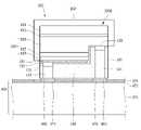
도 1은 실시 예에 따른 광학 렌즈의 측 단면도이다.
도 2는 도 1의 광학 렌즈를 갖는 발광 모듈의 측 단면도이다.
도 3은 도 1의 광학 렌즈의 입사면 및 제1광 출사면의 곡률 반경의 중심을 나타낸 도면이다.
도 4는 도 1의 광학 렌즈를 입사면 및 출사면의 광 분포를 나타낸 도면이다.
도 5는 도 1의 광학 렌즈의 입사면을 설명하기 위한 도면이다.
도 6은 도 1의 광학 렌즈의 제1 및 제2광 출사면의 출사각을 설명하기 위한 도면이다.
도 7은 도 1의 광학 렌즈의 측면도이다.
도 8은 도 1의 광학 렌즈의 저면도이다.
도 9는 도 1의 광학 렌즈에서 제2광 출사면에 의해 반사된 광의 경로를 설명하기 위한 도면이다.
도 10은 도 1의 광학 렌즈에서 바닥면의 다른 예를 나타낸 도면이다.
도 11은 도 1의 광학 렌즈의 제2광 출사면의 다른 예를 나타낸 도면이다.
도 12는 실시 예에 따른 지지 돌기를 갖는 광학 렌즈 및 흡수 층을 갖는 회로 기판을 구비한 발광 모듈의 예시도이다.
도 13은 도 12의 발광 모듈의 광학 렌즈의 투시도이다.
도 14는 실시 예에 따른 광학 렌즈를 갖는 라이트 유닛을 나타낸 측 단면도이다.
도 15는 도 1의 광학 렌즈의 입사면의 곡선 구간을 베지어 곡선 함수를 이용하여 정의하는 일 예를 도시한 도면이다.
도 16은 도 1의 광학 렌즈의 제1광 출사면의 곡선 구간을 베지어 곡선 함수를 이용하여 정의하는 일 예를 도시한 도면이다.
도 17은 실시 예에 따른 회로 기판 상에 배치된 발광 소자의 상세 구성을 나타낸 제1예이다.
도 18은 실시 예에 따른 회로 기판 상에 배치된 발광 소자의 제2예이다.
도 19는 실시 예에 따른 회로 기판 상에 배치된 발광 소자의 제3예를 나타낸 도면이다.
도 20은 실시 예에 따른 발광 모듈을 갖는 표시 장치를 나타낸 도면이다.
도 21은 실시 예와 비교 예의 휘도 분포를 나타낸 도면이다.
도 22는 실시 예에 따른 광학 렌즈의 출사 광의 변화를 나타낸 도면이다.
도 23은 실시 예에 따른 광학 렌즈에 있어서, 제2광 출사면의 요철 여부에 따른 휘도 분포를 나타낸 그래프이다.
도 24는 실시 예에 따른 광학 렌즈에 있어서, 제2광 출사면의 요철 여부에 따른 색차 변화를 나타낸 그래프이다.
도 25는 실시 예에 따른 광학 렌즈에 있어서, 회로기판의 흡수층 여부에 따른 화상 균일도를 나타낸 그래프이다.1 is a side cross-sectional view of an optical lens according to an embodiment.
FIG. 2 is a side cross-sectional view of the light emitting module having the optical lens of FIG. 1 .
FIG. 3 is a view showing the centers of radii of curvature of the incident surface and the first light output surface of the optical lens of FIG. 1 .
FIG. 4 is a view showing light distribution of an incident surface and an exit surface of the optical lens of FIG. 1 .
FIG. 5 is a view for explaining an incident surface of the optical lens of FIG. 1 .
FIG. 6 is a view for explaining emission angles of first and second light exit surfaces of the optical lens of FIG. 1 .
FIG. 7 is a side view of the optical lens of FIG. 1 .
FIG. 8 is a bottom view of the optical lens of FIG. 1 .
FIG. 9 is a view for explaining a path of light reflected by a second light emitting surface in the optical lens of FIG. 1 .
FIG. 10 is a view showing another example of a bottom surface of the optical lens of FIG. 1 .
11 is a view showing another example of a second light emitting surface of the optical lens of FIG. 1 .
12 is an exemplary view of a light emitting module including an optical lens having a support protrusion and a circuit board having an absorption layer according to an embodiment.
13 is a perspective view of an optical lens of the light emitting module of FIG. 12 .
14 is a side cross-sectional view illustrating a light unit having an optical lens according to an embodiment.
15 is a diagram illustrating an example of defining a curved section of an incident surface of the optical lens of FIG. 1 using a Bezier curve function.
16 is a diagram illustrating an example of defining a curved section of a first light emitting surface of the optical lens of FIG. 1 using a Bezier curve function.
17 is a first example illustrating a detailed configuration of a light emitting device disposed on a circuit board according to an embodiment.
18 is a second example of a light emitting device disposed on a circuit board according to an embodiment.
19 is a diagram illustrating a third example of a light emitting device disposed on a circuit board according to an embodiment.
20 is a diagram illustrating a display device having a light emitting module according to an exemplary embodiment.
21 is a view showing the luminance distribution of Examples and Comparative Examples.
22 is a diagram illustrating a change in light emitted from an optical lens according to an embodiment.
23 is a graph showing the luminance distribution according to whether the second light exit surface is uneven in the optical lens according to the embodiment.
24 is a graph illustrating a color difference change according to whether a second light emitting surface is uneven in the optical lens according to the embodiment.
25 is a graph showing image uniformity according to whether or not an absorption layer of a circuit board exists in the optical lens according to the embodiment.
이하, 실시 예들은 첨부된 도면 및 실시 예들에 대한 설명을 통하여 명백하게 드러나게 될 것이다. 실시 예들의 설명에 있어서, 각 층(막), 영역, 패턴 또는 구조물들이 기판, 각 층(막), 영역, 패드 또는 패턴들의 "상/위(on)"에 또는 "하/아래(under)"에 형성되는 것으로 기재되는 경우에 있어, "상/위(on)"와 "하/아래(under)"는 "직접(directly)" 또는 "다른 층을 개재하여 (indirectly)" 형성되는 것을 모두 포함한다. 또한 각 층의 상/위 또는 하/아래에 대한 기준은 도면을 기준으로 설명한다.Hereinafter, the embodiments will be clearly revealed through the accompanying drawings and the description of the embodiments. In the description of the embodiments, each layer (film), region, pattern or structure is “on” or “under/under” the substrate, each layer (film), region, pad or pattern. In the case of being described as being “formed on,” “on” and “under/under” both refer to “directly” or “indirectly” formed through another layer. include In addition, the criteria for the upper / upper or lower / lower of each layer will be described with reference to the drawings.
이하, 첨부된 도면을 참조하여 실시 예에 따른 광학 렌즈 및 이를 구비한 발광 모듈을 설명한다.Hereinafter, an optical lens and a light emitting module having the same according to an embodiment will be described with reference to the accompanying drawings.
도 1은 실시 예에 따른 광학 렌즈의 측 단면도이고, 도 2는 도 1의 광학 렌즈를 갖는 발광 모듈의 측 단면도이다.1 is a side cross-sectional view of an optical lens according to an embodiment, and FIG. 2 is a side cross-sectional view of a light emitting module having the optical lens of FIG. 1 .
도 1 및 도 2를 참조하면, 발광 모듈(301)은, 발광 소자(100), 상기 발광 소자(100) 상에 배치된 광학 렌즈(300), 및 상기 발광 소자(100) 아래에 배치된 회로 기판(400)을 포함한다.1 and 2 , the
상기 발광 소자(100)는 상기 회로 기판(400) 상에 소정의 간격을 갖고 배열될 수 있다. 상기 발광 소자(100)는 상기 광학 렌즈(300)와 상기 회로 기판(400) 사이에 배치되고, 상기 회로 기판(400)으로부터 전원을 공급받아 구동하며 광을 방출하게 된다.The
상기 발광 소자(100)는 도 2와 같이, 상면(S1) 및 다수의 측면(S2)을 통해 광을 방출하게 되며, 예컨대 5면 또는 그 이상의 발광 면을 갖는다. 상기 발광 소자(100)의 다수의 측면(S2)은 적어도 4개의 측면을 포함한 구조로서, 발광 면일 수 있다.The
상기 발광 소자(100)는 5면 이상의 발광 면을 제공하므로, 측면(S2)을 통해 방출된 광에 의해 광의 지향각 분포는 넓어질 수 있다. 상기 발광 소자(100)의 광의 지향각 분포는 140도 이상 예컨대, 142도 이상이 될 수 있다. 상기 발광 소자(100)의 지향각 분포의 반치폭은 70도 이상, 예컨대 71도 이상일 수 있다. 상기 반치폭은 지향각의 최대 광도의 1/2 광도을 갖는 폭을 나타낸다. 이러한 발광 소자(100)의 광의 지향각 분포를 넓게 제공해 줌으로써, 광학 렌즈(300)를 이용한 광 확산이 보다 용이한 효과가 있다.Since the
상기 발광 소자(100)는 화합물 반도체를 갖는 LED 칩 예컨대, UV(Ultraviolet) LED 칩, 청색 LED 칩, 녹색 LED 칩, 백색 LED 칩, 적색 LED 칩 중 적어도 하나를 포함할 수 있다. 상기 발광 소자(100)는 II족-VI족 화합물 반도체 및 III족-V족 화합물 반도체 중 적어도 하나 또는 모두를 포함할 수 있다. 상기 발광 소자(100)는 청색, 녹색, 청색, UV 또는 백색의 광 중 적어도 하나를 발광할 수 있다.
The
상기 광학 렌즈(300)는 발광 소자(100)로부터 방출된 광(light)의 경로를 변경한 후 외부로 추출시켜 줄 수 있다. 상기 발광 소자(100)는 광원으로 정의될 수 있다.The
상기 광학 렌즈(300)는, 바닥면(310), 상기 바닥면(310)보다 위로 볼록한 리세스(recess)(315), 상기 리세스(315)의 둘레에 입사면(320), 상기 바닥면(310) 및 상기 입사면(320)의 반대측에 배치된 제1광 출사면(330), 및 상기 제1광 출사면(330)의 하부 둘레에 배치된 제2광 출사면(335)을 포함한다.The
상기 광학 렌즈(300)는 상기 발광 소자(100)로부터 방출된 광을 입사면(320)으로 입사받아 제1 및 제2광 출사면(330,335)로 방출하게 된다. 상기 입사면(320)으로부터 입사된 일부 광은 소정의 경로를 거쳐 상기 바닥면(310)으로 방출될 수 있다.The
광학 렌즈(300)는 상기 발광 소자(100)로부터 방출된 광이 136도 이상의 지향각 분포를 갖고 입사면(320)으로 입사되면, 제1 및 제2광 출사면(330,335)을 통해 확산시켜 줄 수 있다.When the light emitted from the
상기 광학 렌즈(300)의 입사면(320)은 상기 발광 소자(100)의 다수의 측면(S2)과 서로 대면하게 배치되므로, 상기 발광 소자(100)의 측면(320)으로부터 방출된 광이 직접 입사될 수 있다. 이에 따라 상기 발광 소자(100)의 측면(S2)으로 방출된 광은 누설 없이 입사면(320)으로 입사될 수 있다.Since the
상기 발광 소자(100)의 상면에 대해 연직한 방향은 광축(Y0) 방향이라 할 수 있다. 상기 광축(Y0) 방향은 상기 회로 기판(400)의 상면에 직교하는 방향일 수 있다. 상기 광축(Y0)과 직교하는 제1축(X0) 방향은 상기 발광 소자(100)로부터 상기 광축(Y0)에 직교하는 방향일 수 있다.
A direction perpendicular to the upper surface of the
상기 리세스(315)는 바닥면(310)의 센터 영역으로부터 광축(Y0) 방향으로 함몰된 형태이다. 상기 리세스(315)는 센터 영역 또는 광축(Y0)에 가까울수록 더 깊은 깊이를 가질 수 있다. 상기 리세스(315)의 너비(D1)는 광축(Y0) 방향(예: 상 방향)으로 진행할수록 점차 좁아질 수 있다. 상기 리세스(315)는 위로 올라갈수록 제1광 출사면(330)에 더 인접할 수 있다.The
상기 리세스(315)의 측 단면 형상은 반구 형상 또는 반 타원 형상을 포함할 수 있으며, 그 표면의 하부 형상은 원 형상 또는 다각형 형상을 포함할 수 있다. 상기 입사면(320)은 바닥면(310)의 센터 영역으로부터 위로 볼록한 리세스(315)의 둘레에 배치된다.The cross-sectional shape of the side of the
상기 입사면(320)은 베지어(Bezier) 곡선을 갖는 회전체로 형성될 수 있다. 상기 입사면(320)의 곡선은 스플라인(Spline) 예컨대, 큐빅(cubic), B-스플라인, T-스플라인으로 구현될 수 있다. 상기 입사면(320)의 곡선은 베지어 곡선(Bezier curve)로 구현될 수 있다.
The
상기 입사면(320)은 상기 리세스(315)의 표면으로서 상기 발광 소자(100)의 상면(S1) 및 측면(S2)의 외측에 배치될 수 있다.The
상기 광학 렌즈(300)의 바닥면(310)은 평평한 면, 곡면 또는 곡면과 플랫한 면을 포함할 수 있다. 상기 바닥면(310)은 상기 회로 기판(400)의 상면에 대해 경사진 면을 제공할 수 있다. 상기 광학 렌즈(300)의 바닥면(310)은 제1축(X0)을 기준으로 경사진 면으로 제공될 수 있다. 상기 바닥면(310)은 80% 이상의 영역이 상기 회로 기판(400)의 상면에 대해 경사지게 배치될 수 있다. 상기 바닥면(310)은 전 반사면을 포함할 수 있다.The
상기 광학 렌즈(300)의 바닥면(310)은 제1에지(23) 및 제2에지(25)를 포함한다. 상기 제1에지(23)는 상기 입사면(320)과 상기 바닥면(310) 사이의 경계 지점이며, 광학 렌즈(300)의 저점이 될 수 있다. 상기 제1에지(23)는 바닥면(310)의 영역 중에서 가장 낮은 지점이 될 수 있다. 상기 제1에지(23)의 위치는 수평한 선을 기준으로 제2에지(25)보다 낮게 위치될 수 있다. 상기 제1에지(23)는 상기 입사면(320)의 하부 둘레가 될 수 있다.The
상기 제2에지(25)는 제2광 출사면(335)의 하부 둘레 또는 바닥면(310)의 최 외곽에 배치될 수 있다. 상기 제2에지(25)는 상기 바닥면(310)과 상기 제2광 출사면(335) 사이의 경계 지점일 수 있다The
상기 제1에지(23)와 제2에지(25)는 상기 바닥면(310)의 양 끝단일 수 있다. 상기 제1에지(23)는 바텀 뷰 형상이 원 형상 또는 타원 형상일 수 있으며, 상기 제2에지(25)는 바텀 뷰 형상이 원 형상 또는 타원 형상일 수 있다.The
상기 회로 기판(400)의 상면은 광학 렌즈(300)의 바닥면(310)의 제2에지(25)보다 제1에지(23)에 더 인접하게 배치될 수 있다. 상기 바닥면(310)의 제1에지(23)는 상기 회로 기판(400)의 상면에 접촉될 수 있고, 상기 제2에지(25)는 회로 기판(400)의 상면으로부터 최대 간격(T0)으로 이격될 수 있다. 상기 제2에지(25)는 발광 소자(100) 내의 활성층보다 낮은 위치에 배치될 수 있어, 광의 손실을 방지할 수 있다.
The top surface of the
상기 광학 렌즈(300)의 제1 및 제2광 출사면(330,335)은 입사된 광을 굴절시켜 방출하게 된다. 상기 제2광 출사면(335)은 광축(Y0)을 기준으로, 굴절 후의 추출된 광의 각도가 굴절 전에 입사된 광의 각도보다 작게 굴절시켜 준다. 이에 따라 인접한 광학 렌즈(300)간의 광 간섭 거리를 길게 제공할 수 있고, 제2광 출사면(335)을 통해 출사된 일부 광과 제1광 출사면(330)으로 출사된 광이 광학 렌즈(300)의 주변에서 서로 혼색될 수 있다.
The first and second
상기 광학 렌즈(300)의 제1광 출사면(330)은 전 영역으로 광이 출사되는 구면으로 형성될 수 있다. 상기 제1광 출사면(330)의 센터 영역은 정점(31) 또는 고점이 될 수 있으며, 상기 정점(31)으로부터 연속적으로 연결되는 곡면 형상을 포함한다. 상기 제1광 출사면(330)은 입사되는 광을 반사하거나 굴절시켜 외부로 출사시켜 줄 수 있다. 상기 제1광 출사면(330)은 광축(Y0)을 기준으로, 제1광 출사면(330)으로 방출된 광의 굴절 후의 방출 각도는 굴절 전에 입사된 입사 각도보다 클 수 있다.The first
상기 광학 렌즈(300)의 제1광 출사면(330)은 광의 지향각 분포의 반치각 내에서 광축(Y0)을 거리에 따라 단조가 증가하게 되며, 상기 제2광 출사면(335)은 광의 지향각 분포의 반치각을 벗어난 영역을 포함하며, 상기 광축(Y0)을 기준으로 거리에 따라 단조가 감소하게 된다.The monotony of the first
상기 제1광 출사면(330)은 베지어(Bezier) 곡선을 갖는 회전체로 형성될 수 있다. 상기 제1광 출사면(330)의 곡선은 스플라인(Spline) 예컨대, 큐빅(cubic), B-스플라인, T-스플라인으로 구현될 수 있다. 상기 제1광 출사면(330)의 곡선은 베지어 곡선(Bezier curve)로 구현될 수 있다. 이러한 광학 렌즈(300)는 광축(Y0)을 기준으로 회전 대칭 형상으로 제공될 수 있다.The first
상기 제1광 출사면(330)의 센터 영역은 광축(Y0)의 인접 영역으로서, 상 방향으로 볼록한 곡면이거나 평탄한 면일 수 있다. 상기 제1광 출사면(330)의 센터 영역과 제2광 출사면(335) 사이의 영역은 볼록한 곡면 형상으로 제공될 수 있다.The center region of the first
상기 입사면(320) 및 제1광 출사면(330)은 양의 곡률 반경을 가질 수 있다. 상기 제1광 출사면(330)의 센터 영역 및 그 둘레 영역은 음의 곡률 반경을 갖지 않고 서로 다른 양의 곡률 반경을 가질 수 있다. 상기 제1광 출사면(330)의 센터 영역은 곡률 반경이 0인 영역을 포함할 수 있다.The
상기 입사면(320)의 곡률 반경은 상기 제1광출사면(330)의 곡률 반경보다는 작을 수 있다. 또는 상기 입사면(320)은 기울기가 상기 제1광 출사면(330)의 기울기보다는 클 수 있다.
A radius of curvature of the
상기 제2광 출사면(335)은 제1광 출사면(330)의 하부 둘레에 배치되어 입사된 광을 굴절시켜 방출하게 된다. 상기 제2광 출사면(335)은 비구면 형상 또는 플랫(flat) 면을 포함한다. 상기 제2광 출사면(335)은 예컨대 상기 회로 기판(400)의 상면에 대해 수직한 면이거나 경사진 면일 수 있다. 상기 제2광 출사면(335)이 경사진 면으로 형성될 경우, 사출 성형시 분리가 용이한 효과가 있다.The second
상기 제2광 출사면(335)은 상기 광학 렌즈(300)에서 가장 외측에 배치될 수 있다. 상기 제2광 출사면(335)은 상기 제1광 출사면(330)의 하부 둘레에 플랫한 면으로 연장될 수 있다. 상기 제2광 출사면(335)은 제1광 출사면(330)에 인접한 제3에지(35)를 포함할 수 있다. 상기 제2에지(25)는 제2광 출사면(335)의 하부 에지일 수 있으며, 제3에지(35)는 제2광 출사면(335)의 상부 에지이거나 제1 및 제2광 출사면(330,335) 사이의 경계 지점일 수 있다.The second
상기 제2광 출사면(335)은 발광 소자(100)의 측면(S2)으로 방출된 일부 광을 입사받아 굴절시켜 추출하게 된다. 이때 제2광 출사면(335)은 광축(Y0)을 기준으로, 방출된 광의 출사 각이 굴절 전의 입사각보다 작을 수 있다. 이에 따라 인접한 광학 렌즈(300) 간의 광 간섭 거리를 길게 제공할 수 있다.
The second
도 1을 참조하면, 상기 광학 렌즈(300)는 너비(D4)가 두께(D3)보다 넓게 배치될 수 있다. 상기 너비(D4)는 상기 두께(D3)의 2.5배 이상 예컨대, 3배 이상이 될 수 있다. 상기 광학 렌즈(300)의 너비(D4)는 15mm이상일 수 있다. 이러한 광학 렌즈(300)의 너비(D4)가 두께(D3)보다 상기의 범위로 넓게 배치되므로, 라이트 유닛 예컨대, 백라이트 유닛의 전 영역에 균일한 휘도 분포를 제공할 수 있고, 또한 라이트 유닛의 두께를 줄여줄 수 있다.Referring to FIG. 1 , the
여기서, 광학 렌즈(300)의 입사면(320)의 하부 너비(D1)는 상기 리세스(315)의 하부 너비일 수 있으며, 상기 발광 소자(100)의 너비(W1)보다는 넓게 배치될 수 있다. 이러한 입사면(320) 및 리세스(315)는 상기 발광 소자(100)로부터 방출된 광이 용이하게 입사될 수 있는 크기를 갖는다.Here, the lower width D1 of the
상기 리세스(315)의 깊이(D2)는 상기 입사면(320)의 하부 너비(D1)와 같거나 깊게 배치될 수 있다. 상기 리세스(315)의 깊이(D2)는 광학 렌즈(300)의 두께(D3)의 75% 이상 예컨대, 80% 이상의 깊이를 가질 수 있다. 상기 리세스(315)의 깊이(D2)는 상기 제1광 출사면(330)의 정점(31)과 바닥면(310) 또는 제1에지(23)사이의 거리의 80% 이상일 수 있다. 상기 리세스(315)의 깊이(D2)가 깊게 배치됨으로써, 제1광 출사면(330)의 센터 영역이 전 반사면 또는 음의 곡률을 갖지 않더라도, 입사면(320)의 정점(21)의 인접 영역에서도 측 방향으로 광을 확산시켜 줄 수 있다. 상기 리세스(315)의 깊이(D2)는 입사면(320)의 정점(21)의 깊이로서, 상기 입사면(320)의 정점(21)의 깊이가 깊게 배치됨으로써, 정점(21) 및 그 주변 영역으로 입사된 광에 대해 측 방향으로 굴절시켜 줄 수 있다.
A depth D2 of the
상기 입사면(320)의 하부 너비(D1)과 상기 발광 소자(100)의 너비(W1)의 비율(D1:W1)은 1.8: 1 내지 3.0: 1 범위일 수 있다. 상기 입사면(320)의 하부 너비(D1)는 상기 발광 소자(100)의 너비(W1)의 3배 이하로 배치된 경우, 상기 발광 소자(100)로부터 방출된 광이 입사면(320)을 통해 효과적으로 입사될 수 있다.A ratio (D1:W1) of the lower width D1 of the
상기 입사면(320) 중에서 상기 발광 소자(100)과 동일한 너비를 갖는 위치는 상기 입사면(320)의 정점(21)으로부터 소정 거리(D6)로 이격될 수 있다. 상기 거리(D6)는 상기 리세스(315)와 상기 제1광 출사면(330) 사이의 최소 거리(D5)와 같거나 0.1mm 이내의 차이를 가질 수 있다. 이는 발광 소자(100)의 상면(S1)을 통해 방출된 광이 상기 입사면(320)의 정점(21) 주변까지 면 광원 형태로 입사되도록 가이드할 수 있다.A position having the same width as that of the
상기 입사면(320) 중에서 상기 발광 소자(100)과 동일한 너비를 갖는 위치에서 제1광 출사면(330)의 정점(31)까지의 거리(D8)는 0.5mm 내지 2mm 범위로서, 거리(D5) 또는 거리(D6)의 2배일 수 있다. 이는 발광 소자(100)과 동일한 너비를 갖는 입사면(320)의 영역이 상기 제1광 출사면(330)의 정점(31)에 2mm 이하의 거리에 위치하게 됨으로써, 상기 제1광 출사면(330)의 센터 영역이 음의 곡률 반경을 갖지 않더라도, 입사면(310)의 깊이(D2)와 상기 정점(31)과의 거리에 의해 측 방향으로 광을 확산시켜 줄 수 있다.A distance D8 from a position having the same width as that of the
상기 리세스(315)의 정점(21)과 상기 리세스(315) 내에서 너비(W1) 사이의 거리(D6)는, 상기 리세스(315)의 정점(21)과 상기 제1광 출사면(330)의 정점(31) 사이의 거리(D5)의 비율은 0.5:1 내지 1:1를 범위를 만족한다.
The distance D6 between the apex 21 of the
상기 리세스(315)와 상기 제1광 출사면(330) 사이의 최소 거리(D5)는 상기 리세스(315)의 정점(21)과 제1광 출사면(330)의 정점(31) 사이의 간격일 수 있다. 상기 거리(D5)는 예컨대 1.5mm 이하일 수 있으며, 예컨대, 0.6mm 내지 1mm 범위일 수 있다. 상기 리세스(315)의 정점(21)과 제1광 출사면(330) 정점(31) 사이의 거리(D5)가 1.5mm 이상인 경우 상기 제1광 출사면(330)의 센터 영역으로 진행하는 광량이 많아질 수 있어, 핫 스팟 현상이 발생될 수 있다. 상기 리세스(315)의 정점(21)과 제2광 출사면(31) 사이의 거리(D5)가 0.6mm 미만인 경우 광학 렌즈(300)의 센터 측 강성이 약해지는 문제가 있다. 이러한 리세스(315) 및 제1광 출사면(330) 사이의 거리(D5)를 상기 범위로 배치함으로써, 제2광 출사면(335)의 센터 영역이 전 반사면 또는 음의 곡률을 갖지 않더라도, 센터 영역의 주변으로 광의 경로를 수평 방향으로 확산시켜 줄 수 있다. 이는 리세스(35)의 정점(21)이 상기 제1광 출사면(330)의 볼록한 정점(31)에 인접할수록 상기 입사면(320)을 통해 제1광 출사면(330)의 측 방향으로 진행하는 광의 광량이 증가될 수 있다. 따라서, 광학 렌즈(300)의 측 방향으로 확산하는 광량을 증가시켜 줄 수 있다.The minimum distance D5 between the
상기 리세스(315)의 정점(21)은 상기 제2광 출사면(335)의 제3에지(35)로부터 수평하게 연장한 직선보다는 제1광 출사면(330)의 센터인 정점(31)에 더 인접하게 배치될 수 있다.
The apex 21 of the
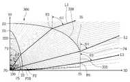
도 3을 참조하면, 광학 렌즈(300)에서 상기 제1광 출사면(330)은 서로 다른 곡률 반경(ra, rb, rc)을 갖는 복수의 원 성분을 가질 수 있으며, 상기 서로 다른 원 성분의 중심(Pa,Pb,Pc)은 서로 다른 위치에 배치될 수 있다. 이러한 제1광 출사면(330)의 원 성분들의 중심(Pa,Pb,Pc)은 상기 입사면(320)의 정점(21)의 수평한 직선보다 아래에 배치될 수 있다. 상기 제1광 출사면(330)의 원 성분들의 중심(Pa,Pb,Pc)은 상기 광학 렌즈(300)와 수직 방향으로 오버랩된 영역에 배치될 수 있다.Referring to FIG. 3 , in the
상기 입사면(320)은 서로 다른 곡률 반경을 갖는 복수의 원 성분을 가질 수 있으며, 상기 원 성분의 중심은 상기 입사면(320)의 정점(21)의 수평한 직선보다 아래에 배치될 수 있고, 상기 광학 렌즈(300)와 수직 방향으로 오버랩된 영역에 배치될 수 있다.The
도 4를 참조하면, 광학 렌즈(300)의 광 경로를 보면, 상기 발광 소자(100)로부터 방출된 광 중에서 광학 렌즈(300)의 입사면(320)의 제1지점(P1)으로 입사된 제1광(L1)은 굴절되어 제1광 출사면(330)의 소정의 제2지점(P2)으로 방출될 수 있다. 또한 상기 발광 소자(100)로부터 방출된 광 중에서 상기 입사면(320)의 제3지점(P3)으로 입사된 제2광(L2)은 제2광 출사면(335)의 소정의 제4지점(P4)으로 방출될 수 있다.Referring to FIG. 4 , looking at the optical path of the
여기서, 상기 광축(Y0)을 기준으로 입사면(320)의 제1지점(P1)으로 입사되는 제1광(L1)의 입사 각도를 제1각도(θ1)로 정의하고, 상기 광축(Y0)을 기준으로 제1광 출사면(330)의 임의의 제3지점(P2)으로 방출된 제1광(L1)의 방출 각도를 제2각도(θ2)로 정의할 수 있다. 상기 광축(Y0)을 기준으로 입사면(320)의 제3지점(P3)으로 입사되는 제2광(L2)의 입사 각도를 제3각도(θ3)로 정의하고, 상기 광축(Y0)을 기준으로 제2광 출사면(335)의 제4지점(P4)으로 출사된 제2광(L2)의 방출 각도를 제4각도(θ4)로 정의할 수 있다. 상기 제2광(L2)은 발광 소자(100)의 측면으로 방출된 광일 수 있다.Here, an incident angle of the first light L1 incident on the first point P1 of the
상기 제2각도(θ2)는 상기 제1각도(θ1)보다 크게 된다. 상기 제2각도(θ2)는 상기 제1각도(θ1)가 점차 커질수록 점차 커지게 되며, 상기 제1각도(θ1)가 점차 작아질수록 점차 작아지게 된다. 그리고 제1 및 제2각도(θ1, θ2)는 θ2>θ1 또는 1<(θ2/θ1)의 조건을 만족한다. 상기 제1광 출사면(330)의 제2각도(θ2)는 굴절 후의 방출 각도로서, 굴절 전의 입사 각도보다 클 수 있다. 이에 따라 제1광 출사면(330)은 입사면(320)을 통해 입사된 광 중에서 상기 제1광 출사면(330)으로 진행하는 제1광(L1)에 대해 굴절시켜 줌으로써, 제1광(L1)에 대해 광학 렌즈(300)의 측 방향으로 확산시켜 줄 수 있다.The second angle θ2 is greater than the first angle θ1 . The second angle θ2 gradually increases as the first angle θ1 gradually increases, and gradually decreases as the first angle θ1 decreases as the first angle θ1 decreases. In addition, the first and second angles θ1 and θ2 satisfy the condition of θ2>θ1 or 1<(θ2/θ1). The second angle θ2 of the first
상기 제4각도(θ4)는 상기 제3각도(θ3)보다 작을 수 있다. 상기 제3각도(θ3)가 증가할수록 상기 제4각도(θ4)는 증가하게 되며, 상기 제3각도(θ3)가 감소할수록 상기 제4각도(θ4)는 감소하게 된다. 그리고 제3 및 제4각도(θ3, θ4)는 θ4<θ3 또는 1>(θ4/θ3)의 조건을 만족한다. 상기 제2광 출사면(335)의 제4각도(θ4)는 굴절 후의 방출 각도로서, 굴절 전의 입사 각도보다 작을 수 있다. 상기 제2광 출사면(335)에는 발광 소자(100)의 측면(S2)을 통해 방출된 광이거나 광 지향각을 벗어난 광들이 입사될 수 있다. 이에 따라 상기 제2광 출사면(335)는 발광 소자(100)의 측면(S2)을 통해 방출된 광 및 광 지향각 분포를 벗어난 광에 대해, 휘도 분포의 반치각 영역 이내로 진행하도록 굴절시켜 줄 수 있다. 상기 제2광 출사면(335)에 의해 광 손실을 줄일 수 있다.The fourth angle θ4 may be smaller than the third angle θ3 . As the third angle θ3 increases, the fourth angle θ4 increases, and as the third angle θ3 decreases, the fourth angle θ4 decreases. In addition, the third and fourth angles θ3 and θ4 satisfy the condition of θ4<θ3 or 1>(θ4/θ3). The fourth angle θ4 of the second
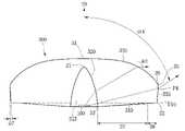
상기 제2광 출사면(335)의 제3에지(35)는 상기 광축(Y0)에 대해 상기 발광 소자(100)의 지향각 분포의 반치각 예컨대, 제4각도(θ4)의 위치 보다 위에 배치될 수 있다. 예컨대, 광축(Y0)과 기준점(P0)부터 제3에지(35) 사이를 연결하는 직선 사이의 각도는 상기 발광 소자(100)의 반치각보다 작을 수 있다.The
발광 소자(100)로부터 방출된 광 중에서 반치각에 인접한 영역으로 조사된 광은 상기 제2광 출사면(335)을 통해 방출되도록 제어할 수 있다. 이 경우 제2광 출사면(335)으로 방출된 제2광(L2)은 제1광 출사면(330)으로 진행하는 광들과 혼색될 수 있다.Among the light emitted from the
여기서, 상기 기준점(P0)는 광축(Y0)과 발광 소자(100)의 교점일 수 있다. 상기 기준점(P0)은 발광 소자(100)의 상면(S1)보다 낮은 위치에 배치될 수 있다. 상기 발광 소자(100)의 기준점(P0)은 상면(S1)의 중심과 복수의 측면(S2)의 중심이 교차되는 지점이거나 상기 상면(S1)의 중심과 각 측면(S2)의 하부 중심이 교차되는 지점이 될 수 있다. 이러한 기준점(P0)은 광축(Y0)과 발광 소자(100)로부터 출사된 광이 교차되는 교점이 될 수 있다. 상기 기준점(P0)은 상기 광학 렌즈(300)의 저점과 동일한 수평 선상에 배치되거나 더 높은 위치에 배치될 수 있다.
Here, the reference point P0 may be an intersection of the optical axis Y0 and the
상기 발광 소자(100)로부터 방출된 광 중에서 입사면(320)의 제5지점(P5)로 입사된 광(L3)은 상기 광학 렌즈(300)의 바닥면(310)에 의해 반사되고 제2광 출사면(335)의 제6지점(P6)을 통해 투과 또는 반사될 수 있다. 이때 상기 제2광 출사면(335)은 바닥면(310)으로부터 반사되어 입사된 광의 입사각(θ8)보다 작은 출사각(θ9)으로 광을 투과 또는 반사하게 된다. 상기 입사각(θ8) 및 출사각(θ9)은 광축(Y0)과의 각도이다. 여기서, 상기 바닥면(310)에 의해 반사되어 제2광 출사면(335)으로 진행하는 광은 입사각(θ8)보다 출사각(θ8)이 작게 굴절됨으로써, 발광 소자(100)의 측면(S2)을 통해 누설될 수 있는 광을 효과적으로 재 사용할 수 있다. 또한 발광 소자(100)의 광 지향각 분포에서 반치 각을 벗어나는 광에 대해서도 상기 바닥면(310)에 의한 전 반사를 통해 광 누설을 방지할 수 있는 효과가 있다.Among the light emitted from the
도 22는 제1,2광 출사면으로 출사된 출사각과 입사면의 입사각의 비율을 나타낸 도면이다. 도 22와 같이, 제1광 출사면(330)의 영역(A1)은 출사각/입사각의 비율이 제2광 출사면(335)의 영역(A2)에 인접할수록 점차 작아지게 되며, 1보다 큰 비율을 가지게 된다. 도 22의 X축 방향은 광의 지향각을 나타내는 것으로서, 68도의 이상의 광의 지향각 분포는 제2광 출사면(335)의 영역(A2)에 의해 제어될 수 있다.22 is a diagram illustrating a ratio of an exit angle emitted to the first and second light exit surfaces to an incident angle of the incident surface. As shown in FIG. 22 , the area A1 of the first
상기 제2광 출사면(335)의 영역(A2)에서 1보다 작은 값을 가지게 되며, 바닥면(310)에 의해 제2광 출사면(335)로 반사된 영역(A3)을 통해 출사된 광의 출사각/입사각의 비율은 상기 영역(A2)보다 작은 값을 가지게 된다.It has a value less than 1 in the area A2 of the second
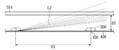
발광 소자(100)의 측면(S2)으로 방출된 광 중에서 제2광 출사면(335)을 통해 방출된 광은 입사 각도보다 작은 방출 각도로 방출되므로, 도 14와 같이 광학 렌즈(100) 간의 간격(G1) 즉, 광 간섭 거리를 늘려줄 수 있다. 또한 광학 렌즈(300)에 의한 휘도 분포가 개선되므로, 회로 기판(400)과 광학 시트(514) 사이의 거리(H1)를 줄여줄 수 있다. 또한 백라이트 유닛 내에 배치된 광학 렌즈(300)의 개수를 줄여줄 수 있다.
Among the light emitted to the side surface S2 of the
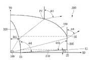
도 5를 참조하면, 상기 광학 렌즈(300)에서 바닥면(310)의 제1에지(23)의 위치는 상기 발광 소자(300)의 기준점(P0)보다 낮거나 같은 위치에 위치할 수 있으며, 제2에지(25)의 위치는 상기 발광 소자(100)의 상면(S1)보다 높게 배치될 수 있으며, 이에 대해 한정하지는 않는다. 이에 따라 상기 바닥면(310)은 상기 입사면(320)로부터 입사된 발광 소자(100)의 측면(S2)을 통해 방출된 광을 전 반사하게 된다.5, the position of the
상기 광학 렌즈(300)는 기준점(P0), 입사면(320)의 정점(21), 및 상기 입사면(320)의 제1에지(23)를 연결한 선분은 삼각형 형상 예컨대, 직각 삼각형 형상으로 제공될 수 있다. 상기 광축(Y0)의 기준 점(P0)과 정점(21)과 제1에지(23)을 연결한 선분 사이의 각도(θ11)는 30도 이하 예컨대, 20도 내지 24도일 수 있다. 이러한 각도(θ12)는 다른 각도(θ14)의 1/3배 이하일 수 있다.
The
도 1 및 도 5를 참조하면, 상기 리세스(315)와 수직 방향으로 오버랩되는 제1광 출사면(330)의 센터 영역이 평탄한 면이거나 볼록한 면으로 처리됨으로써, 리세스(315)의 깊이(도 1의 D2)가 낮을 경우 상기 제1광 출사면(330)의 센터 영역으로 투과되는 광에 의해 핫 스팟이 발생될 수 있다. 실시 예는 리세스(315)의 깊이(D2)를 상기 제1광 출사면(330)의 볼록한 센터 영역에 인접하게 배치하여, 상기 리세스(315)의 입사면(320)에 의해 광을 측 방향으로 굴절시켜 줄 수 있다. 이에 따라 광학 렌즈(300)의 제1광 출사면(330)에 의해 출사된 광에 의한 핫 스팟은 줄어들 수 있다.1 and 5 , the center region of the first
상기 기준 점(P0)을 광축(Y0)과 정점(31) 및 제1에지(23) 사이의 각도(θ13)는 상기 각도(θ11)보다 작은 15도 내지 22도 범위일 수 있다. 여기서, 상기 각도 θ11/θ12 < 1를 만족하며, 상기 각도 θ11/θ5 > 1을 만족한다. 여기서, 각도(θ5)는 바닥면(310)의 경사진 각도이다. 상기 각도 θ11는 각도 θ5보다 4배 이상 예컨대, 5배 이상 20배 이하의 범위를 갖는다.
An angle θ13 between the optical axis Y0 of the reference point P0 and the
도 6을 참조하면, 상기 광학 렌즈(300)에서 바닥면(310)의 경사진 각도(θ5)는 5도 이내일 수 있으며, 예컨대 0.5도 내지 4도 범위일 수 있다. 상기 바닥면(310)의 양 에지(23,25)를 연결한 제1직선(X1)과 광축(Y0)이 이루는 각도(θ6)는 예각 예컨대, 89.5도 이하일 수 있으며, 예컨대 87도 이하일 수 있다. 이러한 바닥면(310)이 경사진 각도(θ5)를 갖는 면으로 배치됨으로써, 발광 소자(100)의 측면(S2)을 통해 입사된 광을 반사하여 제2광 출사면(335)을 통해 투과 또는 반사시켜 준다. 상기 제2광 출사면(335)의 출사각은 반사면(310)을 통해 입사된 입사각보다 작게 출사하게 됨으로써, 인접한 광학 렌즈 간의 간섭을 줄여줄 수 있다. 이에 따라 광학 렌즈(300)의 제2광 출사면(335)을 통해 방출된 광량을 개선시켜 줄 수 있다.Referring to FIG. 6 , the inclined angle θ5 of the
상기 바닥면(310)의 경사진 각도(θ5)는 도 11에 개시된, 제2광 출사면(335)의 경사진 각도(θ7)보다 클 수 있다.
The inclined angle θ5 of the
그리고, 상기 바닥면(310)에서 제2에지(25) 및 제3에지(35) 사이의 직선 거리는 상기 리세스(315)의 깊이(D2)보다 작을 수 있다. 상기 제2광 출사면(335)의 너비(D7)는 상기 리세스(315)와 상기 제1광 출사면(330) 사이의 거리의 1.5배 이상 예컨대, 2배 이상일 수 있다. 상기 제2광 출사면(335)의 제3에지(35)와 기준점(P0)을 연결하는 직선과 광축(Y0) 사이의 각도는 상기 발광 소자(100)의 지향각 분포의 반치각 예컨대, 각도(θ4)보다 작을 수 있다. 여기서, 상기 반치각은 발광 소자(100)로부터 방출된 광 출력이 광축을 기준으로 피크치의 50% 또는 1/2이 되는 각도를 나타낸다.
In addition, the linear distance between the
상기 제2광 출사면(335)의 영역 중에서, 제2지점(P2)를 출사하는 출사각(θ2)이 발광 소자(100)의 지향각 분포의 반치각의 1/2 지점인 경우, 상기 제2지점(P2)로 입사되는 광의 입사면(320)의 지점과 광축(Y0) 사이의 거리(D11)는 상기 D1의 1/2 이하의 지점일 수 있다. 이는 광학 렌즈(300)의 두께를 줄이거나 제1광출사면(330)의 정점 높이를 낮추더라도, 광을 측 방향으로 확산시켜 줄 수 있다.In the region of the second
상기 광축(Y0)에 대해 상기 광학 렌즈(300)의 바닥면(310)의 제1에지(23)를 연결한 선분 사이의 제6각도(θ6)는 상기 선분과 제2광 출사면(335) 사이의 각도(θ61)보다 작을 수 있다. 상기 각도 θ6/θ61 < 1를 만족할 수 있다. 여기서, 상기 각도 θ6는 90도 미만일 수 있으며, 상기 각도 θ61은 90도 이상 예컨대, 90< θ61 ≤ 95도 범위일 수 있다. 이러한 광학 렌즈(300)의 바닥면(310)의 선분은 광축(Y0)에 대해 예각을 갖고, 제2광 출사면(335)에 대해 둔각을 갖게 되므로, 발광 소자(100)로부터 방출된 광을 전반사시켜 줄 수 있고, 또한 상기 전 반사된 광을 제2광 출사면(335)을 통해 굴절됨으로써, 다른 광학 렌즈와의 간섭을 줄여줄 수 있다.
A sixth angle θ6 between the line segment connecting the
한편, 상기 광학 렌즈(300)는 하부에 배치된 하나 또는 복수의 지지 돌기(미도시)를 포함한다. 상기 지지 돌기는 상기 광학 렌즈(300)의 바닥면(310)으로부터 하 방향 즉, 회로 기판(400) 방향으로 돌출된다. 상기 지지 돌기는 복수개가 회로 기판(400) 상에 고정되며, 상기 광학 렌즈(300)가 틸트되는 것을 방지할 수 있다.
Meanwhile, the
도 2와 같이, 상기 회로 기판(400)은 표시 장치, 단말기, 조명 장치와 같은 라이트 유닛 내에 배열될 수 있다. 상기 회로 기판(400)은 상기 발광 소자(100)와 전기적으로 연결되는 회로 층을 포함할 수 있다. 상기 회로 기판(400)은 수지 재질의 PCB, 금속 코어를 갖는 PCB(MCPCB, Metal Core PCB), 연성 PCB(FPCB, Flexible PCB) 중 적어도 하나를 포함할 수도 있으며, 이에 대해 한정하지는 않는다.
As shown in FIG. 2 , the
도 7 및 도 8은 실시 예에 따른 광학 렌즈의 측면도 및 배면도를 나타낸 도면이다.7 and 8 are views showing a side view and a rear view of an optical lens according to an embodiment.
도 7을 참조하면, 상기 광학 렌즈(300)는 제2광 출사면(335)에 요철 면을 구비할 수 있다. 상기 요철 면은 표면이 거친 헤이즈(Haze) 면으로 형성될 수 있다. 상기 요철 면은 산란 입자가 형성된 면일 수 있다.Referring to FIG. 7 , the
도 8을 참조하면, 상기 광학 렌즈(300)의 바닥면(310)은 요철 면을 구비할 수 있다. 상기 요철 면은 표면이 거친 헤이즈 면으로 형성되거나, 산란 입자가 형성될 수 있다.Referring to FIG. 8 , the
도 23을 참조하면, 예1은 바닥면 및 측면에 헤이즈가 처리되지 않는 광학 렌즈에서의 휘도 분포의 변화를 나타낸 것이며, 예2는 바닥면 및 측면에 헤이즈가 처리된 광학 렌즈에서의 휘도 분포의 변화를 나타낸 것이다. 여기서, 광학 렌즈의 측면 및 바닥 면에 헤이즈가 처리된 예2에서 균일도가 개선됨을 알 수 있다.Referring to FIG. 23 , Example 1 shows the change in luminance distribution in an optical lens in which haze is not applied to the bottom and side surfaces, and Example 2 is the luminance distribution in the optical lens in which haze is applied to the bottom and side surfaces of the optical lens. indicates change. Here, it can be seen that the uniformity is improved in Example 2 in which haze is applied to the side and bottom surfaces of the optical lens.
도 24을 참조하면, 예1은 헤이즈가 처리되지 않는 광학 렌즈에서의 색차 변화를 나타낸 것이며, 예2는 헤이즈가 처리된 광학 렌즈에서의 색차 변화를 나타낸 것이다. 헤이즈가 처리된 예2에서 색차 개선 효과가 있음을 알 수 있다.
Referring to FIG. 24 , Example 1 shows a change in color difference in an optical lens to which haze is not treated, and Example 2 shows a change in color difference in an optical lens in which haze is treated. It can be seen that in Example 2 in which the haze was treated, there was an effect of improving the color difference.
도 9와 같이, 광학 렌즈(300)의 제2광 출사면(335) 및 바닥면(310)에 요철 면이 형성된 경우, 상기 입사면(320)으로 입사된 광은 상기 바닥면(310)에 의해 전 반사될 수 있다. 상기 제2광 출사면(335)은 입사된 일부 광을 반사하게 되며, 상기 반사된 일부 광은 상기 입사면(320)으로 재 입사되어 굴절되거나 제1광 출사면(330)으로 직접 입사될 수 있다. 여기서, 상기 제2광 출사면(335)에 의해 반사된 광 중에서 입사면(320)으로 입사된 광량은 상기 제1광 출사면(330)으로 입사된 광량보다 더 많을 수 있다. 상기 입사면(320)으로 재 입사된 광은 굴절되어 제1광 출사면(330) 또는 제2광 출사면(335)을 통해 출사될 수 있다.
As shown in FIG. 9 , when uneven surfaces are formed on the second
여기서, 도 9 및 도 10과 같이, 광학 렌즈(300)의 바닥면(310)은 곡면을 갖는 제1영역(D9)과 평탄 면을 갖는 제2영역(D10)을 포함한다. 상기 바닥면(310)은 리세스(315)에 인접한 영역이 곡면을 갖고 상기 제2광 출사면(335)에 입접한 영역이 평평한 면으로서, 수평한 면이거나 경사진 면으로 제공될 수 있다.Here, as shown in FIGS. 9 and 10 , the
상기 제1영역(D9)은 제1에지(23)부터 위로 볼록한 곡률 반경을 갖게 된다. 즉, 상기 바닥면(310)에서 제1영역(D9)의 곡면은 수평한 연장 선에 대해 위로 오목하게 되며, 예컨대 65mm 내지 75mm 범위의 곡률 반경을 갖는다. 즉, 상기 제1영역(D9)는 음(-)의 곡률을 가질 수 있다. 상기 제2영역(D10)은 상기 제1영역(D9)과 제2에지(25) 사이에 배치된다. 상기 제1영역(D9)의 너비가 제2영역(D10)의 너비보다 더 넓을 수 있다. 상기 제1영역(D9)과 제2영역(D10)의 길이 비율은 6:4 내지 9:1의 비율로 배치될 수 있다. 상기 제1영역(D7)의 너비가 넓을수록 광학 렌즈(300)의 중심부에서의 핫 스팟 현상을 줄여줄 수 있다.The first region D9 has a radius of curvature convex upward from the
상기 바닥면(310) 중에서 곡면 구간인 제1영역(D9)은 상기 입사면(320)에 인접하게 배치되며, 상기 평탄한 구간인 제2영역(D10)은 제2에지(25)에 인접하게 배치될 수 있다. 상기 곡면 및 평탄 면은 제1에지(23)부터 제2에지(25)를 직선으로 연결한 선분보다 위에 배치될 수 있다. 상기 제1영역(D9)은 상기 제2에지(25)의 수평 연장 선보다 낮게 배치되며, 상기 제2영역(D10)은 상기 제2에지(25)의 수평 연장 선과 동일 선상에 배치될 수 있다.Of the
상기 바닥면(310)의 제1영역(D9)은 상기 발광 소자(100)로부터 방출된 광을 다른 방향으로 굴절시켜 주어, 제1 및 제2광 출사면(330,335)에 의한 휘도 분포를 변화시켜 줄 수 있다. 이러한 광의 휘도 분포는 바닥면(310)이 곡면 영역을 포함할 경우, 중심부의 핫 스팟 현상이 경사진 면을 갖는 광학 렌즈에 비해 개선될 수 있다.
The first region D9 of the
도 11은 실시 예에 따른 광학 렌즈의 다른 예이다.11 is another example of an optical lens according to an embodiment.
도 11을 참조하면, 광학 렌즈의 제2광 출사면(335)은 수직한 광축(Y0)을 기준으로, 제7각도(θ7)로 경사질 수 있다. 상기 제7각도(θ7)는 제5각도(θ5)보다 작을 수 있다. 상기 각도 θ7/ θ5 <1을 만족할 수 있다.
Referring to FIG. 11 , the second
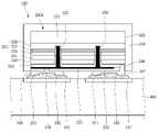
도 12 및 도 13는 실시 예에 따른 발광 모듈에서 회로 기판 상에 흡수층을 배치한 구조이다.12 and 13 are structures in which an absorption layer is disposed on a circuit board in a light emitting module according to an embodiment.
도 12 및 도 13을 참조하면, 회로 기판(400) 상에 흡수층(412,414)을 배치된다. 광학 렌즈(300)의 제1광 출사면(330)에 입사된 광의 일부(L5)는 투과되고 일부 광(L6)은 반사된다. 상기 흡수층(412,414)은 입사되는 광(L6)을 흡수하게 된다. 상기 흡수층(412,414)은 흑색 레지스트 물질을 포함할 수 있다.12 and 13 , absorption layers 412 and 414 are disposed on the
상기 흡수층(412,414)은 광학 렌즈(300)와 수직 방향으로 오버래되는 영역에 배치될 수 있다. 상기 흡수층(412,414)은 상기 광학 렌즈(300)의 바닥면(310)과 수직 방향으로 오버랩되는 영역에 배치될 수 있다. 상기 흡수층(412,414)은 상기 회로 기판(400)의 상기 광학 렌즈(300)의 리세스(315)를 기준으로 서로 반대측에 배치될 수 있다.
The absorption layers 412 and 414 may be disposed in a region overlapping the
상기 광학 렌즈(300)의 너비(D4)가 상기 회로 기판(400)의 너비(D13)보다 넓은 경우, 상기 광학 렌즈(300)가 배열되는 방향을 따라 상기 광학 렌즈(300)의 리세스(315)의 양측에 상기 흡수층(412,414)이 각각 배치될 수 있다. 이러한 흡수층(412,414)은 상기 광학 렌즈(300)의 제1광 출사면(330)으로 반사된 일부 광(L6)이 입사된 경우 흡수하게 된다.When the width D4 of the
상기 흡수층(412,414)의 영역은 상기 제1광 출사면(330)으로 반사된 광의 광량이 최대인 영역 아래에 배치될 수 있다. 상기 흡수층(412,414)의 영역들은 상기 광축(Y0)의 기준점으로부터 동일한 반경(D12)을 갖고 배치될 수 있다.Regions of the absorption layers 412 and 414 may be disposed under regions in which the amount of light reflected by the first
도 25와 같이, 회로 기판 상에 흡수층을 갖는 경우(예3)는 흡수층을 갖지 않는 경우(예4)에 비해, 불필요한 광을 흡수하게 되므로, 광의 균일도가 개선됨을 알 수 있다.As shown in FIG. 25 , it can be seen that the case in which the absorbing layer is provided on the circuit board (Example 3) absorbs unnecessary light compared to the case in which the absorbing layer is not provided (Example 4), so that the light uniformity is improved.
도 12 및 도 13을 참조하면, 상기 광학 렌즈(300)의 바닥 면(310)에는 복수의 지지 돌기(350,355)이 배치될 수 있다. 상기 복수의 지지 돌기(350,355)는 제1지지 돌기(350) 및 제2지지 돌기(355)를 포함한다. 상기 제1지지 돌기(350)는 상기 흡수층(412,414)의 영역을 제외하고 복수개가 배치될 수 있으며, 회로 기판(400)의 상면과 접촉될 수 있다. 상기 제1지지 돌기(350)은 2개 또는 3개 이상으로 배치되어, 회로 기판(400) 상에 광학 렌즈(300)을 지지하게 된다.12 and 13 , a plurality of
상기 제2지지 돌기(355)는 상기 제1지지 돌기(350)의 높이보다 더 높이 돌출될 수 있다. 상기 제2지지 돌기(355) 간의 간격은 상기 회로 기판(400)의 너비(D13)과 동일하거나 더 이격될 수 있다. 상기 제2지지 돌기(355) 사이에는 상기 회로 기판(400)이 끼워질 수 있다. 이에 따라 제2지지 돌기(355)는 광학 렌즈(300)를 결합하는 과정에서 상기 회로 기판(400)의 외측에 결합되어 상기 광학 렌즈(300)가 틸트되는 것을 방지할 수 있다. 상기 제2지지 돌기(355)는 2개 또는 3개 이상이 배치될 수 있으며, 상기 회로 기판(400)의 양측에 접촉될 수 있다. 상기 제2지지 돌기(355)의 반경은 상기 제1지지 돌기(350)의 반경보다 클 수 있다.
The
도 14은 실시 예에 따른 광학 렌즈를 갖는 라이트 유닛을 나타낸 측 단면도이다.14 is a side cross-sectional view illustrating a light unit having an optical lens according to an embodiment.
도 14를 참조하면, 각 회로 기판(400) 내에 배치된 광학 렌즈(300) 간의 간격(G1)은 서로 다른 회로 기판(400) 내에 배치된 광학 렌즈(300) 간의 간격보다 좁게 배열될 수 있다. 상기 간격(G1)은 도 13에 도시된 광학 렌즈(300)의 너비(D4)의 6배 내지 10배 범위 예컨대, 7배 내지 9배 범위로 배열될 수 있다. 상기 광학 렌즈(300) 간의 간격(G1)은 인접한 광학 렌즈(300) 간의 광 간섭을 방지할 수 있다.Referring to FIG. 14 , the spacing G1 between the
여기서, 상기 광학 렌즈(300)의 너비(D4)는 15mm 이상이 될 수 있으며, 예컨대 16mm 내지 20mm 범위에 있을 수 있다. 상기 광학 렌즈(300)의 너비(D4)가 상기 범위보다 좁은 경우 라이트 유닛 내의 광학 렌즈의 개수가 증가될 수 있고 상기 광학 렌즈(300)들 사이의 영역에 암부가 발생될 수 있다. 상기 광학 렌즈(300)의 너비(D4)가 상기 범위보다 넓은 경우 라이트 유닛 내의 광학 렌즈의 개수는 감소되지만, 각 광학 렌즈의 휘도가 감소될 수 있다.Here, the width D4 of the
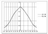
도 21은 라이트 유닛에서의 광학 렌즈의 휘도 분포를 나타낸 것으로서, 실시 예는 비교 예의 광학 렌즈를 출사면이 음의 곡률 반경을 갖는 구조에 비해, 거의 동일한 휘도 분포를 가지게 된다.
21 is a diagram showing the luminance distribution of the optical lens in the light unit, and the embodiment has almost the same luminance distribution compared to the optical lens of the comparative example in which the emitting surface has a negative radius of curvature.
한편, 광학 렌즈(300)는 입사면(320) 및 제1광 출사면(330)의 단면이 곡선 구간을 포함하는 경우, 곡선 구간은 비선형적 수치해석 기법인 스플라인 곡선(spline curve)을 만족할 수 있다. 스플라인 곡선은 적은 수의 제어점(control point)으로 매끄러운 곡선을 만들기 위한 함수로서, 선정된 제어점들을 통과하는 보간(interpolation) 곡선, 선정된 제어점을 연결하는 선의 모양에 근사(approximation) 곡선으로 정의될 수 있다. 스플라인 곡선으로는 비스플라인(B-Spline) 곡선, 베지어(Bezier) 곡선, 넙스(Non-UniformRational B-Spline, NURBS) 곡선, 큐빅 스플라인(cubic spline) 곡선 등이 사용될 수 있다.Meanwhile, in the
일 예로, 각 면의 단면에 포함되는 곡선 구간은 베지어 곡선 함수(Bezier Curve equation)를 통하여 나타낼 수 있다. 베지어 곡선 함수는 최초의 제어점(control point)인 시작점과, 최후의 제어점인 끝점 그리고 그 사이에 위치하는 내부 제어점의 이동에 의해 다양한 자유 곡선을 얻는 함수로 구현될 수 있다.
For example, the curved section included in the cross section of each surface may be expressed through a Bezier curve equation. The Bezier curve function may be implemented as a function to obtain various free curves by moving a start point, which is the first control point, an end point, which is the last control point, and an internal control point located therebetween.
도 15는 리세스의 입사면의 곡선을 구하는 것으로서, 시작 점(C1)과 끝점(C2), 그리고 적어도 하나의 내부 제어점(C3)의 이동에 의해 구현될 수 있다.15 shows a curve of the incident surface of the recess, which may be implemented by moving a start point C1, an end point C2, and at least one internal control point C3.
상기 내부 제어점(C3)과 연결되는 상기 시작 점(C1)과 끝점(C2)에 대한 가중치(weight)를 주어 상기의 입사면(320)의 곡선을 아래의 표 1과 같이 구할 수 있다. 표 1은 입사면의 곡선 구간을 구하기 위한 파라미터들이다.By giving weights to the start point C1 and the end point C2 connected to the internal control point C3, the curve of the
상기 시작 점(C1)의 X축 지점과 가중치(Weight)는 광학 렌즈(300)와 광학 시트 사이의 간격에 따라 변경될 수 있다.
The X-axis point and the weight of the starting point C1 may be changed according to the distance between the
도 16은 광학 렌즈의 제1광 출사면의 곡선을 구하는 것으로서, 시작 점(C4)과 끝점(C5), 그리고 적어도 두 개의 내부 제어점(C6,C7)의 이동에 의해 구현될 수 있다.16 shows a curve of the first light emitting surface of the optical lens, which may be implemented by moving a start point C4 and an end point C5, and at least two internal control points C6 and C7.
상기 내부 제어점(C6,C7)과 연결되는 상기 시작 점(C4)과 끝점(C5)에 대한 가중치(weight)를 주어 상기의 제1광 출사면(330)의 곡선을 아래의 표2와 같이 구할 수 있다. 표 2는 제1광 출사면의 곡선 구간을 구하기 위한 파라미터들이다.By giving weights to the start point C4 and the end point C5 connected to the internal control points C6 and C7, the curve of the first
상기 시작 점(C4)의 X축 지점과 가중치(Weight)는 광학 렌즈(300)와 광학 시트 사이의 간격에 따라 변경될 수 있다.
The X-axis point and the weight of the starting point C4 may be changed according to the distance between the
도 17은 실시 예에 따른 발광 소자(100)의 제1예를 나타낸 도면이다. 도 17을 참조하여 발광 소자(100) 및 회로 기판(400)을 설명하기로 한다.17 is a view showing a first example of the
도 17을 참조하면, 상기 발광 소자(100)는 발광 칩(100A)을 포함한다. 상기 발광 소자(100)는 발광 칩(100A)과 상기 발광 칩(100A) 상에 배치된 형광체층(150)을 포함할 수 있다. 상기 형광체층(150)은 청색, 녹색, 황색, 적색 형광체 중 적어도 하나 또는 복수를 포함하며, 단층 또는 다층으로 배치될 수 있다. 상기 형광체층(150)은 투광성 수지 재료 내에 형광체가 첨가된다. 상기 투광성 수지 재료는 실리콘 또는 에폭시와 같은 물질을 포함하며, 상기 형광체는 YAG, TAG, Silicate, Nitride, Oxy-nitride 계 물질 중에서 선택적으로 형성될 수 있다.Referring to FIG. 17 , the
상기 형광체층(150)은 상기 발광 칩(100A)의 상면에 배치되거나, 상기 발광 칩(100A)의 상면 및 측면에 배치될 수 있다. 상기 형광체층(150)은 상기 발광 칩(100A)의 표면 중에서 광이 방출되는 영역 상에 배치되어, 광의 파장을 변환시켜 줄 수 있다.The
상기 형광체층(150)은 단층 또는 서로 다른 형광체층을 포함할 수 있으며, 상기 서로 다른 형광체층은 제1층이 적색, 황색, 녹색 형광체 중 적어도 한 종류의 형광체를 가질 수 있고, 제2층이 상기 제1층 위에 형성되며 적색, 황색, 녹색 형광체 중 상기 제1층과 다른 형광체를 가질 수 있다. 다른 예로서, 상기 서로 다른 형광체층은 3층 이상의 형광체층을 포함할 수 있으며, 이에 대해 한정하지는 않는다.The
다른 예로서, 상기 형광체층(150)은 필름 타입을 포함할 수 있다. 상기 필름 타입의 형광체층은 균일한 두께를 제공함으로써, 파장 변환에 따른 색 분포가 균일할 수 있다.As another example, the
상기 발광 칩(100A)에 대해 설명하면, 상기 발광 칩(100A)은 기판(111), 제1반도체층(113), 발광 구조물(120), 전극층(131), 절연층(133), 제1전극(135), 제2전극(137), 제1연결 전극(141), 제2연결 전극(143), 및 지지층(140)을 포함할 수 있다.When describing the
상기 기판(111)은 투광성, 절연성 또는 도전성 기판을 이용할 수 있으며, 예컨대, 사파이어(Al2O3), SiC, Si, GaAs, GaN, ZnO, Si, GaP, InP, Ge, Ga2O3 중 적어도 하나를 이용할 수 있다. 상기 기판(111)의 탑 면 및 바닥면 중 적어도 하나 또는 모두에는 복수의 볼록부(미도시)가 형성되어, 광 추출 효율을 개선시켜 줄 수 있다. 각 볼록부의 측 단면 형상은 반구형 형상, 반타원 형상, 또는 다각형 형상 중 적어도 하나를 포함할 수 있다. 여기서, 상기 기판(111)은 발광 칩(100A) 내에서 제거될 수 있으며, 이 경우 상기 제1반도체층(113) 또는 제1도전형 반도체층(115)이 발광 칩(100A)의 탑 층으로 배치될 수 있다.The
상기 기판(111) 아래에는 제1반도체층(113)이 형성될 수 있다. 상기 제1반도체층(113)은 II족 내지 V족 원소의 화합물 반도체를 이용하여 형성될 수 있다. 상기 제1반도체층(113)은 II족 내지 V족 원소의 화합물 반도체를 이용하여 적어도 한 층 또는 복수의 층으로 형성될 수 있다. 상기 제1반도체층(113)은 예컨대, III족-V족 원소의 화합물 반도체를 이용한 반도체층 예컨대, GaN, InN, AlN, InGaN, AlGaN, InAlGaN, AlInN, AlGaAs, GaP, GaAs, GaAsP, AlGaInP, GaP 중 적어도 하나를 포함할 수 있다. 상기 제1반도체층(113)은 InxAlyGa1-x-yN (0≤x≤1, 0≤y≤1, 0≤x+y≤1)의 조성식을 갖고, 버퍼층 및 언도프드(undoped) 반도체층 중 적어도 하나로 형성될 수 있다. 상기 버퍼층은 상기 기판과 질화물 반도체층 간의 격자 상수의 차이를 줄여줄 수 있고, 상기 언도프드 반도체층은 반도체의 결정 품질을 개선시켜 줄 수 있다. 여기서, 상기 제1반도체층(113)은 형성하지 않을 수 있다.A
상기 제1반도체층(113) 아래에는 발광 구조물(120)이 형성될 수 있다. 상기 발광 구조물(120)은 II족 내지 V족 원소 및 III족-V족 원소의 화합물 반도체 중에서 선택적으로 형성되며, 자외선 대역부터 가시 광선 대역의 파장 범위 내에서 소정의 피크 파장을 발광할 수 있다.A
상기 발광 구조물(120)은 제1도전형 반도체층(115), 제2도전형 반도체층(119), 상기 제1도전형 반도체층(115)과 상기 제2도전형 반도체층(119) 사이에 형성된 활성층(117)을 포함하며, 상기 각 층(115,117,119)의 위 및 아래 중 적어도 하나에는 다른 반도체층이 더 배치될 수 있으며, 이에 대해 한정하지는 않는다.The
상기 제1도전형 반도체층(115)은 제1반도체층(113) 아래에 배치되며, 제1도전형 도펀트가 도핑된 반도체 예컨대, n형 반도체층으로 구현될 수 있다. 상기 제1도전형 반도체층(115)은 InxAlyGa1-x-yN (0≤x≤1, 0≤y≤1, 0≤x+y≤1)의 조성식을 포함한다. 상기 제1도전형 반도체층(115)은 III족-V족 원소의 화합물 반도체 예컨대, GaN, AlN, AlGaN, InGaN, InN, InAlGaN, AlInN, AlGaAs, GaP, GaAs, GaAsP, AlGaInP 중에서 선택될 수 있다. 상기 제1도전형 도펀트는 n형 도펀트로서, Si, Ge, Sn, Se, Te 등과 같은 도펀트를 포함한다.The first conductivity
상기 활성층(117)은 제1도전형 반도체층(115) 아래에 배치되고, 단일 양자 우물, 다중 양자 우물(MQW), 양자 선(quantum wire) 구조 또는 양자 점(quantum dot) 구조를 선택적으로 포함하며, 우물층과 장벽층의 주기를 포함한다. 상기 우물층/장벽층의 주기는 예컨대, InGaN/GaN, GaN/AlGaN, AlGaN/AlGaN, InGaN/AlGaN, InGaN/InGaN, AlGaAs/GaA, InGaAs/GaAs, InGaP/GaP, AlInGaP/InGaP, InP/GaAs의 페어 중 적어도 하나를 포함한다.The
상기 제2도전형 반도체층(119)은 활성층(117) 아래에 배치된다. 상기 제2도전형 반도체층(119)은 제2도전형 도펀트가 도핑된 반도체 예컨대, InxAlyGa1-x-yN (0≤x≤1, 0≤y≤1, 0≤x+y≤1)의 조성식을 포함한다. 상기 제2도전형 반도체층(119)은, GaN, InN, AlN, InGaN, AlGaN, InAlGaN, AlInN, AlGaAs, GaP, GaAs, GaAsP, AlGaInP와 같은 화합물 반도체 중 적어도 하나로 이루어질 수 있다. 상기 제2도전형 반도체층(119)이 p형 반도체층이고, 상기 제1도전형 도펀트는 p형 도펀트로서, Mg, Zn, Ca, Sr, Ba을 포함할 수 있다.The second
상기 발광 구조물(120)은 다른 예로서, 상기 제1도전형 반도체층(115)이 p형 반도체층, 상기 제2도전형 반도체층(119)은 n형 반도체층으로 구현될 수 있다. 상기 제2도전형 반도체층(119) 위에는 상기 제2도전형과 반대의 극성을 갖는 제3도전형 반도체층이 형성할 수도 있다. 또한 상기 발광 구조물(120)은 n-p 접합 구조, p-n 접합 구조, n-p-n 접합 구조, p-n-p 접합 구조 중 어느 한 구조로 구현할 수 있다.
As another example of the
상기 제2도전형 반도체층(119) 아래에는 전극층(131)이 형성된다. 상기 전극층(131)은 반사층을 포함할 수 있다. 상기 전극층(131)은 상기 발광 구조물(120)의 제2도전형 반도체층(119)에 접촉된 오믹 접촉층을 포함할 수 있다. 상기 반사층은 반사율이 70% 이상인 물질 예컨대, Al, Ag, Ru, Pd, Rh, Pt, Ir의 금속과 상기의 금속 중 둘 이상의 합금 중에서 선택될 수 있다. 상기 반사층의 금속은 상기 제2도전형 반도체층(119) 아래에 접촉될 수 있다. 상기 오믹 접촉층은 투광성 재질, 금속 또는 비 금속 재질 중에서 선택될 수 있다.An
상기 전극층(131)은 투광성 전극층/반사층의 적층 구조를 포함할 수 있으며, 상기 투광성 전극층은 예컨대 ITO(indium tin oxide), IZO(indium zinc oxide), IZTO(indium zinc tin oxide), IAZO(indium aluminum zinc oxide), IGZO(indium gallium zinc oxide), IGTO(indium gallium tin oxide), AZO(aluminum zinc oxide), ATO(antimony tin oxide), GZO(gallium zinc oxide), Ag, Ni, Al, Rh, Pd, Ir, Ru, Mg, Zn, Pt, Au, Hf 및 이들의 선택적인 조합으로 구성된 물질 중에서 형성될 수 있다. 상기 투광성 전극층의 아래에는 금속 재질의 반사층이 배치될 수 있으며, 예컨대 Ag, Ni, Al, Rh, Pd, Ir, Ru, Mg, Zn, Pt, Au, Hf 및 이들의 선택적인 조합으로 구성된 물질 중에서 형성될 수 있다. 상기 반사층은 다른 예로서, 서로 다른 굴절률을 갖는 두 층이 교대로 배치된 DBR(distributed bragg reflection) 구조로 형성될 수 있다.The
상기 제2도전형 반도체층(119) 및 상기 전극층(131) 중 적어도 한 층의 표면에는 러프니스와 같은 광 추출 구조가 형성될 수 있으며, 이러한 광 추출 구조는 입사되는 광의 임계각을 변화시켜 주어, 광 추출 효율을 개선시켜 줄 수 있다.
A light extraction structure such as roughness may be formed on the surface of at least one of the second
상기 절연층(133)은 상기 전극층(131) 아래에 배치되며, 상기 제2도전형 반도체층(119)의 하면, 상기 제2도전형 반도체층(119) 및 상기 활성층(117)의 측면, 상기 제1도전형 반도체층(115)의 일부 영역에 배치될 수 있다. 상기 절연층(133)은 상기 발광 구조물(120)의 하부 영역 중에서 상기 전극층(131), 제1전극(135) 및 제2전극(137)을 제외한 영역에 형성되어, 상기 발광 구조물(120)의 하부를 전기적으로 보호하게 된다.The insulating
상기 절연층(133)은 Al, Cr, Si, Ti, Zn, Zr 중 적어도 하나를 갖는 산화물, 질화물, 불화물, 및 황화물 중 적어도 하나로 형성된 절연물질 또는 절연성 수지를 포함한다. 상기 절연층(133)은 예컨대, SiO2, Si3N4, Al2O3, TiO2 중에서 선택적으로 형성될 수 있다. 상기 절연층(133)은 단층 또는 다층으로 형성될 수 있으며, 이에 대해 한정하지는 않는다. 상기 절연층(133)은 발광 구조물(120)의 아래에 플립 본딩을 위한 금속 구조물을 형성할 때, 상기 발광 구조물(120)의 층간 쇼트를 방지하기 위해 형성된다.The insulating
상기 절연층(133)은 서로 다른 굴절률을 갖는 제1층과 제2층이 교대로 배치된 DBR(distributed bragg reflector) 구조로 형성될 수 있으며, 상기 제1층은 SiO2, Si3N4, Al2O3, TiO2 중에서 어느 하나이며, 상기 제2층은 상기 제1층 이외의 물질 중 어느 하나로 형성될 수 있으나 이에 한정하지 않으며, 또는 상기 제1층 및 제2층이 동일한 물질로 형성되거나 3층 이상의 층을 갖는 페어(Pair)로 형성될 수도 있다. 이 경우, 상기 전극층은 형성하지 않을 수 있다.
The insulating
상기 제1도전형 반도체층(115)의 일부 영역 아래에는 제1전극(135)이 배치되며, 상기 전극층(131)의 일부 아래에는 제2전극(137)이 배치될 수 있다. 상기 제1전극(135) 아래에는 제1연결 전극(141)이 배치되며, 상기 제2전극(137) 아래에는 제2연결 전극(143)이 배치된다.A
상기 제1전극(135)은 상기 제1도전형 반도체층(115)과 상기 제1연결 전극(141)에 전기적으로 연결되며, 상기 제2전극(137)은 상기 전극층(131)을 통해 상기 제2도전형 반도체층(119)과 제2연결 전극(143)에 전기적으로 연결될 수 있다.The
상기 제1전극(135) 및 제2전극(137)은 Cr, Ti, Co, Ni, V, Hf, Ag, Al, Ru, Rh, Pt, Pd, Ta, Mo, W 중 적어도 하나 또는 합금으로 형성될 수 있으며, 단층 또는 다층으로 형성될 수 있다. 상기 제1전극(135)과 상기 제2전극(137)은 동일한 적층 구조이거나 다른 적층 구조로 형성될 수 있다. 상기 제1전극(135) 및 상기 제2전극(137) 중 적어도 하나는 암(arm) 또는 핑거(finger) 구조와 같은 전류 확산 패턴이 더 형성될 수 있다. 또한 상기 제1전극(135) 및 상기 제2전극(137)은 하나 또는 복수로 형성될 수 있으며, 이에 대해 한정하지는 않는다. 상기 제1 및 제2연결 전극(141,143) 중 적어도 하나는 복수로 배치될 수 있으며, 이에 대해 한정하지는 않는다.The
상기 제1연결 전극(141) 및 상기 제2연결 전극(143)은 전원을 공급하는 리드(lead) 기능과 방열 경로를 제공하게 된다. 상기 제1연결 전극(141) 및 상기 제2연결 전극(143)은 원 형상, 다각 형상, 원 기둥 또는 다각 기둥과 같은 형상 중 적어도 하나를 포함할 수 있다. 상기 제1연결 전극(141) 및 제2연결 전극(143)은 금속 파우더의 재질 예컨대, Ag, Al, Au, Cr, Co, Cu, Fe, Hf, In, Mo, Ni, Si, Sn, Ta, Ti, W 및 이들 금속의 선택적 합금 중 어느 하나로 형성될 수 있다. 상기 제1연결 전극(141) 및 제2연결 전극(143)은 상기 제1전극(135) 및 제2전극(137)과의 접착력 향상을 위하여 In, Sn, Ni, Cu 및 이들의 선택적인 합금 중의 어느 한 금속으로 도금될 수 있다.The
상기 지지층(140)은 열 전도성 재질을 포함하며, 상기 제1전극(135), 상기 제2전극(137), 상기 제1연결 전극(141) 및 상기 제2연결 전극(143)의 둘레에 배치될 수 있다. 상기 지지층(140)의 하면에는 상기 제1 및 제2연결 전극(141,143)의 하면이 노출될 수 있다.The
상기 지지층(140)은 발광 소자(100)를 지지하는 층으로 사용된다. 상기 지지층(140)은 절연성 재질로 형성되며, 상기 절연성 재질은 예컨대, 실리콘 또는 에폭시와 같은 수지층으로 형성된다. 다른 예로서, 상기 절연성 재질은 페이스트 또는 절연성 잉크를 포함할 수 있다. 상기 절연성 재질의 재질은 그 종류는 polyacrylate resin, epoxy resin, phenolic resin, polyamides resin, polyimides rein, unsaturated polyesters resin, polyphenylene ether resin (PPE), polyphenilene oxide resin (PPO), polyphenylenesulfides resin, cyanate ester resin, benzocyclobutene (BCB), Polyamido-amine Dendrimers (PAMAM), 및 Polypropylene-imine, Dendrimers (PPI), 및 PAMAM 내부 구조 및 유기-실리콘 외면을 갖는 PAMAM-OS(organosilicon)를 단독 또는 이들의 조합을 포함한 수지로 구성될 수 있다. 상기 지지층(140)은 상기 절연층(133)과 다른 물질로 형성될 수 있다.The supporting
상기 지지층(140) 내에는 Al, Cr, Si, Ti, Zn, Zr 중 적어도 하나를 갖는 산화물, 질화물, 불화물, 황화물과 같은 화합물들 중 적어도 하나가 첨가될 수 있다. 여기서, 상기 지지층(140) 내에 첨가된 화합물은 열 확산제일 수 있으며, 상기 열 확산제는 소정 크기의 분말 입자, 알갱이, 필러(filler), 첨가제로 사용될 수 있다. 상기 열 확산제는 세라믹 재질을 포함하며, 상기 세라믹 재질은 동시 소성되는 저온 소성 세라믹(LTCC: low temperature co-fired ceramic), 고온 소성 세라믹(HTCC: high temperature co-fired ceramic), 알루미나(alumina), 수정(quartz), 칼슘지르코네이트(calcium zirconate), 감람석(forsterite), SiC, 흑연, 용융실리카(fusedsilica), 뮬라이트(mullite), 근청석(cordierite), 지르코니아(zirconia), 베릴리아(beryllia), 및 질화알루미늄(aluminum nitride) 중 적어도 하나를 포함한다. 상기 세라믹 재질은 질화물 또는 산화물과 같은 절연성 물질 중에서 열 전도도가 질화물이나 산화물보다 높은 금속 질화물로 형성될 수 있으며, 상기 금속 질화물은 예컨대, 열 전도도가 140 W/mK 이상의 물질을 포함할 수 있다. 상기 세라믹 재질은 예컨대, SiO2, SixOy, Si3N4, SixNy, SiOxNy, Al2O3, BN, Si3N4, SiC(SiC-BeO), BeO, CeO, AlN와 같은 세라믹 (Ceramic) 계열일 수 있다. 상기 열 전도성 물질은 C (다이아몬드, CNT)의 성분을 포함할 수 있다.
At least one of compounds such as oxide, nitride, fluoride, and sulfide having at least one of Al, Cr, Si, Ti, Zn, and Zr may be added into the
상기 발광 칩(100A)은 상기 회로 기판(400) 상에 플립 방식으로 탑재된다. 상기 회로 기판(400)은 금속층(471), 상기 금속층(471) 위에 절연층(472), 상기 절연층(472) 위에 복수의 리드 전극(473,474)을 갖는 회로 층(미도시) 및 상기 회로 층을 보호하는 보호층(475)을 포함한다. 상기 금속층(471)은 방열 층으로서, 열 전도성이 높은 금속 예컨대, Cu 또는 Cu-합금와 같은 금속을 포함하며, 단층 또는 다층 구조로 형성될 수 있다.The
상기 절연층(472)은 상기 금속층(471)과 회로 층 사이를 절연시켜 준다. 상기 절연층은 에폭시, 실리콘, 유리섬유, 프리 프레그(prepreg), 폴리프탈아미드(PPA: Polyphthalamide), LCP(Liquid Crystal Polymer), PA9T(Polyamide9T)와 같은 수지 재질 중 적어도 하나를 포함할 수 있다. 또한 상기 절연층(472) 내에는 금속 산화물 예컨대, TiO2, SiO2, Al2O3와 같은 첨가제가 첨가될 수 있으며, 이에 대해 한정하지는 않는다. 다른 예로서, 상기 절연층(472)은 그라핀과 같은 재질을 실리콘 또는 에폭시와 같은 절연 물질 내에 첨가하여 사용할 수 있으며, 이에 대해 한정하지는 않는다.The insulating
상기 절연층(472)은 상기 금속층(471)이 양극 산화(anodizing) 과정에 의해 형성된 아노다이징(anodizing)된 영역일 수 있다. 여기서, 상기 금속층(471)은 알루미늄 재질이고, 상기 아노다이징된 영역은 Al2O3와 같은 재질로 배치될 수 있다.
The insulating
상기 제1 및 제2리드 전극(473,474)은 발광 칩(100A)의 제1 및 제2연결 전극(141,143)과 전기적으로 연결된다. 상기 제1 및 제2리드 전극(473,474)과 상기 발광 칩(100A)의 연결 전극(141,143) 사이에는 전도성 접착제(461,462)가 배치될 수 있다. 상기 전도성 접착제(461,462)는 솔더 재질과 같은 금속 재질을 포함할 수 있다. 상기 제1리드 전극(473) 및 제2리드 전극(474)은 회로 패턴으로서, 전원을 공급해 주게 된다.The first and second lead electrodes 473,474 are electrically connected to the first and
상기 보호층(475)은 상기 회로층 상에 배치될 수 있다. 상기 보호층(475)은 반사 재질을 포함하며, 예컨대 레지스트 재질 예컨대, 백색의 레지스트 재질로 형성될 수 있으며, 이에 대해 한정하지는 않는다. 상기 보호층(475)은 반사층으로 기능할 수 있으며, 예컨대 흡수율보다 반사율이 더 높은 재질로 형성될 수 있다. 다른 예로서, 상기 보호층(475)은 광을 흡수하는 재질로 배치될 수 있으며, 상기 광 흡수 재질은 흑색 레지스트 재질을 포함할 수 있다.
The
도 18을 참조하여 발광 모듈의 발광 소자의 제2예를 설명하기로 한다.A second example of the light emitting device of the light emitting module will be described with reference to FIG. 18 .
도 18을 참조하면, 발광 소자(100)는 발광 칩(100B)을 포함한다. 상기 발광 소자(100)는 발광 칩(100B)과 상기 발광 칩(100B) 상에 배치된 형광체층(150)을 포함할 수 있다. 상기 형광체층(150)은 청색, 녹색, 황색, 적색 형광체 중 적어도 하나 또는 복수를 포함하며, 단층 또는 다층으로 배치될 수 있다. 상기 형광체층(150)은 투광성 수지 재료 내에 형광체가 첨가된다. 상기 투광성 수지 재료는 실리콘 또는 에폭시와 같은 물질을 포함하며, 상기 형광체는 YAG, TAG, Silicate, Nitride, Oxy-nitride 계 물질 중에서 선택적으로 형성될 수 있다.Referring to FIG. 18 , the
상기 형광체층(150)은 상기 발광 칩(100B)의 상면에 배치되거나, 상기 발광 칩(100B)의 상면 및 측면에 배치될 수 있다. 상기 형광체층(150)은 상기 발광 칩(100B)의 표면 중에서 광이 방출되는 영역 상에 배치되어, 광의 파장을 변환시켜 줄 수 있다.The
상기 발광 칩(100B)은 기판(111), 제1반도체층(113), 발광 구조물(120), 전극층(131), 절연층(133), 제1전극(135), 제2전극(137), 제1연결 전극(141), 제2연결 전극(143), 및 지지층(140)을 포함할 수 있다. 상기 기판(111) 및 제2반도체층(113)은 제거될 수 있다.The
발광 소자(100)의 발광 칩(100B)과 회로 기판(400)은 연결 전극(161,162)으로 연결될 수 있으며, 상기 연결 전극(161,162)은 전도성 펌프 즉, 솔더 범프를 포함할 수 있다. 상기 전도성 펌프는 각 전극(135,137) 아래에 하나 또는 복수로 배열될 수 있으며, 이에 대해 한정하지는 않는다. 상기 절연층(133)은 제1 및 제2전극(135,137)을 노출시켜 줄 수 있으며, 상기 제1 및 제2전극(135,137)은 연결 전극(161,162)와 전기적으로 연결될 수 있다.
The
도 19을 참조하여, 발광 소자의 제3예를 설명하기로 한다.A third example of the light emitting device will be described with reference to FIG. 19 .
도 19을 참조하면, 발광 소자(100)는 회로 기판(400)에 연결된 발광 칩(200A)을 포함한다. 상기 발광 소자(100)는 발광 칩(200A)의 표면에 배치된 형광체층(250)을 포함할 수 있다. 상기 형광체층(250)은 입사되는 광의 파장을 변환하게 된다. 상기 발광 소자(100) 상에는 도 4와 같이 광학 렌즈(도 4의 300)가 배치되어 상기 발광 칩(200A)으로부터 방출된 광의 지향 특성을 조절하게 된다.Referring to FIG. 19 , the
상기 발광 칩(200A)은 발광 구조물(225), 및 복수의 패드(245,247)를 포함한다. 상기 발광 구조물(225)은 II족 내지 VI족 원소의 화합물 반도체층 예컨대, III족-V족 원소의 화합물 반도체층 또는 II족-VI족 원소의 화합물 반도체층으로 형성될 수 있다. 상기 복수의 패드(245,247)는 상기 발광 구조물(225)의 반도체층에 선택적으로 연결되며, 전원을 공급하게 된다.The
상기 발광 구조물(225)은 제1도전형 반도체층(222), 활성층(223) 및 제2도전형 반도체층(224)을 포함한다. 상기 발광 칩(200A)은 기판(221)을 포함할 수 있다. 상기 기판(221)은 상기 발광 구조물(225) 위에 배치된다. 상기 기판(221)은 예컨대, 투광성, 절연성 기판, 또는 전도성 기판일 수 있다. 이러한 구성은 도 4의 발광 구조물 및 기판에 대한 설명을 참조하기로 한다.The
상기 발광 칩(200A)은 하부에 패드(245,247)가 배치되며, 상기 패드(245,247)는 제1 및 제2패드(245,247)를 포함한다. 상기 제1 및 제2패드(245,247)는 상기 발광 칩(200A)의 아래에 서로 이격되어 배치된다. 상기 제1패드(245)는 상기 제1도전형 반도체층(222)과 전기적으로 연결되며, 상기 제2패드(247)는 제2도전형 반도체층(224)과 전기적으로 연결된다. 상기 제1 및 제2패드(245,247)은 바닥 형상이 다각형 또는 원 형상이거나, 회로 기판(400)의 제1 및 제2리드 전극(415,417)의 형상과 대응되도록 형성될 수 있다. 상기 제1 및 제2패드(245,247) 각각의 하면 면적은 예컨대, 제1 및 제2리드 전극(415,417) 각각의 상면 크기와 대응되는 크기로 형성될 수 있다.
상기 발광 칩(200A)은 상기 기판(221)과 상기 발광 구조물(225) 사이에 버퍼층(미도시) 및 언도프드 반도체층(미도시) 중 적어도 하나를 포함할 수 있다. 상기 버퍼층은 상기 기판(221)과 반도체층과의 격자 상수 차이를 완화시켜 주기 위한 층으로서, II족 내지 VI족 화합물 반도체 중에서 선택적으로 형성될 수 있다. 상기 버퍼층 아래에는 언도핑된 III족-V족 화합물 반도체층이 더 형성될 수 있으며, 이에 대해 한정하지는 않는다. 상기 기판(221)은 제거될 수 있다. 상기 기판(221)이 제거된 경우 형광체층(250)은 상기 제1도전형 반도체층(222)의 상면이나 다른 반도체층의 상면에 접촉될 수 있다.The
상기 발광 칩(200A)은 제1 및 제2전극층(241,242), 제3전극층(243), 절연층(231,233)을 포함한다. 상기 제1 및 제2전극층(241,242) 각각은 단층 또는 다층으로 형성될 수 있으며, 전류 확산층으로 기능할 수 있다. 상기 제1 및 제2전극층(241,242)은 상기 발광 구조물(225)의 아래에 배치된 제1전극층(241); 및 상기 제1전극층(241) 아래에 배치된 제2전극층(242)을 포함할 수 있다. 상기 제1전극층(241)은 전류를 확산시켜 주게 되며, 상기 제2전극층(241)은 입사되는 광을 반사하게 된다.The
상기 제1 및 제2전극층(241,242)은 서로 다른 물질로 형성될 수 있다. 상기 제1전극층(241)은 투광성 재질로 형성될 수 있으며, 예컨대 금속 산화물 또는 금속 질화물로 형성될 수 있다. 상기 제1전극층은 예컨대 ITO(indium tin oxide), ITON(ITO nitride), IZO(indium zinc oxide), IZON(IZO nitride), IZTO(indium zinc tin oxide), IAZO(indium aluminum zinc oxide), IGZO(indium gallium zinc oxide), IGTO(indium gallium tin oxide), AZO(aluminum zinc oxide), ATO(antimony tin oxide), GZO(gallium zinc oxide) 중에서 선택적으로 형성될 수 있다. 상기 제2전극층(242)은 상기 제1전극층(241)의 하면과 접촉되며 반사 전극층으로 기능할 수 있다. 상기 제2전극층(242)은 금속 예컨대, Ag, Au 또는 Al를 포함한다. 상기 제2전극층(242)은 상기 제1전극층(241)이 일부 영역이 제거된 경우, 상기 발광 구조물(225)의 하면에 부분적으로 접촉될 수 있다.The first and second electrode layers 241,242 may be formed of different materials. The
다른 예로서, 상기 제1 및 제2전극층(241,242)의 구조는 무지향성 반사(ODR: Omni Directional Reflector layer) 구조로 적층될 수 있다. 상기 무지향성 반사 구조는 낮은 굴절률을 갖는 제1전극층(241)과, 상기 제1전극층(241)과 접촉된 고 반사 재질의 금속 재질인 제2전극층(242)의 적층 구조로 형성될 수 있다. 상기 전극층(241,242)은, 예컨대, ITO/Ag의 적층 구조로 이루어질 수 있다. 이러한 상기 제1전극층(241)과 제2전극층(242) 사이의 계면에서 전 방위 반사각을 개선시켜 줄 수 있다.As another example, the structure of the first and second electrode layers 241,242 may be stacked in an Omni Directional Reflector layer (ODR) structure. The non-directional reflective structure may be formed as a stacked structure of a
다른 예로서, 상기 제2전극층(242)은 제거될 수 있으며, 다른 재질의 반사층으로 형성될 수 있다. 상기 반사층은 분산형 브래그 반사(distributed bragg reflector: DBR) 구조로 형성될 수 있으며, 상기 분산형 브래그 반사 구조는 서로 다른 굴절률을 갖는 두 유전체층이 교대로 배치된 구조를 포함하며, 예컨대, SiO2층, Si3N4층, TiO2층, Al2O3층, 및 MgO층 중 서로 다른 어느 하나를 각각 포함할 수 있다. 다른 예로서, 상기 전극층(241,242)은 분산형 브래그 반사 구조와 무지향성 반사 구조를 모두 포함할 수 있으며, 이 경우 98% 이상의 광 반사율을 갖는 발광 칩(200A)을 제공할 수 있다. 상기 플립 방식으로 탑재된 발광 칩(200A)은 상기 제2전극층(242)로부터 반사된 광이 기판(221)을 통해 방출하게 되므로, 수직 상 방향으로 대부분의 광을 방출할 수 있다. 또한 상기 발광 칩(200A)의 측면으로 방출된 광은 반사 시트(600)에 의해 광학 렌즈의 입사면 영역으로 반사될 수 있다.As another example, the
상기 제3전극층(243)은 상기 제2전극층(242)의 아래에 배치되며, 상기 제1 및 제2전극층(241,242)과 전기적으로 절연된다. 상기 제3전극층(243)은 금속 예컨대, 티타늄(Ti), 구리(Cu), 니켈(Ni), 금(Au), 크롬(Cr), 탄탈늄(Ta), 백금(Pt), 주석(Sn), 은(Ag), 인(P) 중 적어도 하나를 포함한다. 상기 제3전극층(243) 아래에는 제1패드(245) 및 제2패드(247)가 배치된다. 상기 절연층(231,233)은 제1 및 제2전극층(241,242), 제3전극층(243), 제1 및 제2패드(245,247), 발광 구조물(225)의 층 간의 불필요한 접촉을 차단하게 된다. 상기 절연층(231,233)은 제1 및 제2절연층(231,233)을 포함한다. 상기 제1절연층(231)은 상기 제3전극층(243)과 제2전극층(242) 사이에 배치된다. 상기 제2절연층(233)은 상기 제3전극층(243)과 제1/2패드(245,247) 사이에 배치된다. 상기 제1 및 제2패드(245,247)는 상기 제1 및 제2리드 전극(415,417)과 동일한 물질을 포함할 수 있다.The
상기 제3전극층(243)은 상기 제1도전형 반도체층(222)과 연결된다. 상기 제3전극층(243)의 연결부(244)는 상기 제1, 2전극층(241, 242) 및 발광 구조물(225)의 하부를 통해 비아 구조로 돌출되며 제1도전형 반도체층(222)과 접촉된다. 상기 연결부(244)는 복수로 배치될 수 있다. 상기 제3전극층(243)의 연결부(244)의 둘레에는 상기 제1절연층(231)의 일부(232)가 연장되어 제3전극층(243과 상기 제1 및 제2전극층(241,242), 제2도전형 반도체층(224) 및 활성층(223) 간의 전기적인 연결을 차단한다. 상기 발광 구조물(225)의 측면에는 측면 보호를 위해 절연 층이 배치될 수 있으며, 이에 대해 한정하지는 않는다.The
상기 제2패드(247)는 상기 제2절연층(233) 아래에 배치되고 상기 제2절연층(233)의 오픈 영역을 통해 상기 제1 및 제2전극층(241, 242) 중 적어도 하나와 접촉되거나 연결된다. 상기 제1패드(245)는 상기 제2절연층(233)의 아래에 배치되며 상기 제2절연층(233)의 오픈 영역을 통해 상기 제3전극층(243)과 연결된다. 이에 따라 상기 제1패드(247)의 돌기(248)는 제1,2전극층(241,242)을 통해 제2도전형 반도체층(224)에 전기적으로 연결되며, 제2패드(245)의 돌기(246)는 제3전극층(243)을 통해 제1도전형 반도체층(222)에 전기적으로 연결된다.The
상기 제1 및 제2패드(245,247)는 상기 발광 칩(200A)의 하부에 서로 이격되며, 상기 회로 기판(400)의 제1 및 제2리드 전극(415,417)와 대면하게 된다. 상기 제1 및 제2패드(245,247)에는 다각형 형상의 리세스(271,273)를 포함할 수 있으며, 상기 리세스(271,273)는 상기 발광 구조물(225)의 방향으로 볼록하게 형성된다. 상기 리세스(271,273)는 상기 제1 및 제2패드(245,247)의 두께와 같거나 작은 깊이를 갖고 형성될 수 있으며, 이러한 리세스(271,273)의 깊이는 상기 제1 및 제2패드(245,247)의 표면적을 증가시켜 줄 수 있다.The first and
상기 제1패드(245) 및 제1리드 전극(415) 사이의 영역 및 상기 제2패드(247) 및 제2리드 전극(417) 사이의 영역에는 접합 부재(255,257)가 배치된다. 상기 접합 부재(255,257)는 전기 전도성 물질을 포함할 수 있으며, 일부는 상기 리세스(271,273)에 배치된다. 상기 제1 및 제2패드(215,217)는 상기 접합 부재(255,257)가 리세스(271,273)에 배치되므로, 상기 접합 부재(255,257)와 제1 및 제2패드(245,247) 간의 접착 면적은 증가될 수 있다. 이에 따라 제1 및 제2패드(245,247)와 제1 및 제2리드 전극(415,417)가 접합되므로 발광 칩(200A)의 전기적인 신뢰성 및 방열 효율을 개선시켜 줄 수 있다.
상기 접합 부재(255,257)는 솔더 페이스트 재질을 포함할 수 있다. 상기 솔더 페이스트 재질은 금(Au), 주석(Sn), 납(Pb), 구리(Cu), 비스무트(Bi), 인듐(In), 은(Ag) 중 적어도 하나를 포함한다. 상기 접합 부재(255,257)는 열 전달을 회로 기판(400)에 직접 전도하기 때문에 열 전도 효율이 패키지를 이용한 구조보다는 개선될 수 있다. 또한 상기 접합 부재(255,257)는 발광 칩(200A)의 제1 및 제2패드(245,247)와의 열 팽창계수의 차이가 적은 물질이므로, 열 전도 효율을 개선시켜 줄 수 있다.The
상기 접합 부재(255,257)는 다른 예로서, 전도성 필름을 포함할 수 있으며, 상기 전도성 필름은 절연성 필름 내에 하나 이상의 도전성 입자를 포함한다. 상기 도전성 입자는 예컨대, 금속이나, 금속 합금, 탄소 중 적어도 하나를 포함할 수 있다. 상기 도전성 입자는 니켈, 은, 금, 알루미늄, 크롬, 구리 및 탄소 중 적어도 하나를 포함할 수 있다. 상기 전도성 필름은 이방성(Anisotropic) 전도 필름 또는 이방성 도전 접착제를 포함할 수 있다.As another example, the
상기 발광 칩(200A)과 상기 회로 기판(400) 사이에는 접착 부재 예컨대, 열전도성 필름을 포함할 수 있다. 상기 열전도성 필름은 폴리에틸렌테레프탈레이트, 폴리부티렌테레프탈레이드, 폴리에틸렌나프탈레이트, 폴리부티렌나프탈레이트 등의 폴리에스터 수지; 폴리이미드 수지; 아크릴 수지; 폴리스티렌 및 아크릴로니트릴-스티렌 등의 스티렌계 수지; 폴리카보네이트 수지; 폴리락트산 수지; 폴리우레탄 수지; 등을 사용할 수 있다. 또한, 폴리에틸렌, 폴리프로필렌, 에틸렌-프로필렌 공중합체와 같은 폴리올레핀 수지; 폴리비닐클로라이드, 폴리비닐리덴클로라이드 등의 비닐 수지; 폴리아미드 수지; 설폰계 수지; 폴리에테르-에테르케톤계 수지; 알릴레이트계 수지; 또는 상기 수지들의 블렌드 중에서 적어도 하나를 포함할 수 있다.An adhesive member, for example, a thermally conductive film may be included between the light emitting
상기 발광 칩(200A)은 회로 기판(400)의 표면 및 발광 구조물(225)의 측면 및 상면을 통해 광을 방출함으로써, 광 추출 효율을 개선시켜 줄 수 있다. 이러한 회로 기판(400) 상에 발광 칩(200A)을 직접 본딩할 수 있어 공정이 간소화될 수 있다. 또한 발광 칩(200A)의 방열이 개선됨으로써, 조명 분야 등에 유용하게 활용될 수 있다.
The
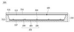
도 20은 실시 예에 따른 발광 모듈을 갖는 표시 장치를 나타낸 측 단면도이다.20 is a side cross-sectional view illustrating a display device having a light emitting module according to an exemplary embodiment.
도 20을 참조하면, 표시 장치(500)는 바텀 커버(510) 상에 발광 모듈(301)이 배치되며, 상기 발광 모듈(301) 상에 광학 시트(514) 및 표시 패널(515)을 포함한다.Referring to FIG. 20 , the
상기 바텀 커버(510)는 방열을 위한 금속 또는 열 전도성 수지 재질을 포함할 수 있다. 상기 바텀 커버(510)는 수납부(560)을 구비하며, 상기 수납부(560)의 둘레에는 측면 커버를 구비할 수 있다.The
상기 발광 모듈(301)은 상기 바텀 커버(510) 상에 하나 또는 복수의 열로 배치될 수 있다. 상기 발광 모듈(301)은 발광 소자(100)에 의해 백색의 광이 방출될 수 있으며, 이에 대해 한정하지는 않는다.The
상기 발광 모듈(301)은 발광 소자(100), 각 발광 소자(100) 상에 광학 렌즈(300), 복수의 발광 소자(100)이 탑재된 회로 기판(400)을 포함한다. 상기 회로 기판(400)은 회로패턴(미도시)을 포함하는 인쇄회로기판(PCB, Printed Circuit Board)일 수 있으며, 예컨대 수지 재질의 PCB, 메탈 코어 PCB(MCPCB, Metal Core PCB), 연성 PCB(FPCB, Flexible PCB) 등을 포함할 수도 있으며, 이에 대해 한정하지는 않는다.The
상기 회로기판(400) 상에는 반사 시트(517)가 배치되며, 상기 반사 시트(517)은 오프 영역(518)을 포함하며, 상기 오픈 영역(518)에는 광학 렌즈(300)가 결합된다. 상기 반사 시트(517)의 오픈 영역(518)을 통해 광학 렌즈(300)가 돌출됨으로써, 광학 렌즈(300)의 방출된 광은 광학 시트(514)를 투과하거나 반사되고, 그 반사된 광은 상기 반사 시트(517)에 의해 재 반사될 수 있다. 이에 따라 백라이트유 유닛(510)의 휘도 분포의 균일도는 개선될 수 있다.A
상기 반사 시트(517)은 예를 들어, PET, PC, PVC 레진 등으로 형성될 수 있으나, 이에 대해 한정하지는 않는다.The
상기 광학 시트는(514)는 분산된 광을 모으는 프리즘 시트들, 휘도강화시트 및 광을 다시 확산시키는 확산 시트 중 적어도 하나를 포함할 수 있다. 상기 광학 시트(514)와 발광 모듈(301) 사이의 영역에는 도광층(미도시)이 배치될 수 있으며, 이에 대해 한정하지는 않는다.The
상기 광학 시트(514) 상에는 표시 패널(515)이 배치될 수 있다. 상기 표시 패널(515)은 입사되는 광에 의해 영상을 표시할 수 있다. 상기 표시 패널(515)은 예컨대, LCD 패널로서, 서로 대향되는 투명한 재질의 제 1 및 제 2기판, 그리고 제 1 및 제 2기판 사이에 개재된 액정층을 포함한다. 상기 표시 패널(515)의 적어도 일면에는 편광판이 부착될 수 있으며, 이러한 편광판의 부착 구조로 한정하지는 않는다. 상기 표시 패널(515)은 광학 시트(514)를 통과한 광에 의해 정보를 표시하게 된다. 이러한 표시 장치(500)는 각 종 휴대 단말기, 노트북 컴퓨터의 모니터, 랩탑 컴퓨터의 모니터, 텔레비젼 등에 적용될 수 있다.A
실시예에 따른 발광 모듈은 라이트 유닛에 적용될 수 있다. 상기 라이트 유닛은 하나 또는 복수의 발광 모듈을 갖는 구조를 포함하며, 3차원 디스플레이, 각종 조명등, 신호등, 차량 전조등, 전광판 등이 포함될 수 있다.
The light emitting module according to the embodiment may be applied to a light unit. The light unit may include a structure having one or a plurality of light emitting modules, and may include a three-dimensional display, various lighting lamps, traffic lights, vehicle headlights, electric signs, and the like.
이상에서 실시예들에 설명된 특징, 구조, 효과 등은 본 발명의 적어도 하나의 실시예에 포함되며, 반드시 하나의 실시예에만 한정되는 것은 아니다. 나아가, 각 실시예에서 예시된 특징, 구조, 효과 등은 실시예들이 속하는 분야의 통상의 지식을 가지는 자에 의해 다른 실시예들에 대해서도 조합 또는 변형되어 실시 가능하다. 따라서 이러한 조합과 변형에 관계된 내용들은 본 발명의 범위에 포함되는 것으로 해석되어야 할 것이다.Features, structures, effects, etc. described in the above embodiments are included in at least one embodiment of the present invention, and are not necessarily limited to only one embodiment. Furthermore, features, structures, effects, etc. illustrated in each embodiment can be combined or modified for other embodiments by those of ordinary skill in the art to which the embodiments belong. Accordingly, the contents related to such combinations and modifications should be interpreted as being included in the scope of the present invention.
또한, 이상에서 실시예를 중심으로 설명하였으나 이는 단지 예시일 뿐 본 발명을 한정하는 것이 아니며, 본 발명이 속하는 분야의 통상의 지식을 가진 자라면 본 실시예의 본질적인 특성을 벗어나지 않는 범위에서 이상에 예시되지 않은 여러 가지의 변형과 응용이 가능함을 알 수 있을 것이다. 예를 들어, 실시예에 구체적으로 나타난 각 구성 요소는 변형하여 실시할 수 있는 것이다. 그리고 이러한 변형과 응용에 관계된 차이점들은 첨부된 청구 범위에서 규정하는 본 발명의 범위에 포함되는 것으로 해석되어야 할 것이다.In addition, although the embodiment has been described above, it is only an example and does not limit the present invention, and those of ordinary skill in the art to which the present invention pertains are exemplified above in a range that does not depart from the essential characteristics of the present embodiment. It can be seen that various modifications and applications that have not been made are possible. For example, each component specifically shown in the embodiment can be implemented by modification. And the differences related to these modifications and applications should be construed as being included in the scope of the present invention defined in the appended claims.
100: 발광 소자100A, 110B, 200A: 발광 칩
301: 발광 모듈150,250: 형광체층
300: 광학 렌즈315: 리세스
320: 입사면310: 바닥면
330: 제1광 출사면335: 제1광 출사면
400: 회로 기판514: 광학 시트
517: 반사 시트100: light emitting
301: light emitting module 150,250: phosphor layer
300: optical lens 315: recess
320: incident surface 310: bottom surface
330: first light exit surface 335: first light exit surface
400: circuit board 514: optical sheet
517: reflective sheet
Claims (21)
Translated fromKorean상기 바닥면으로부터 볼록한 리세스를 갖고 광이 입사되는 입사면;
상기 입사면으로 입사된 광을 방출하고 볼록한 곡면을 갖는 제1광 출사면; 및
상기 제1광 출사면의 외측 하부 둘레에서 상기 바닥면을 향해 연장되는 제2광 출사면을 포함하며,
상기 리세스는 상기 제1광 출사면의 정점과 상기 바닥면 사이의 거리의 80% 이상의 깊이를 가지며,
상기 제1광 출사면의 영역 중 상기 리세스와 수직 방향으로 오버랩된 영역은 볼록한 곡면을 포함하며,
상기 제1광 출사면은 서로 다른 곡률 반경을 갖고, 상기 서로 다른 곡률 반경을 갖는 원들의 중심이 상기 입사면의 정점에 수평한 직선보다 아래에 배치되며,
상기 제2광 출사면은 상기 입사면으로 입사된 제1광의 입사각보다 작은 출사각을 갖고,
상기 바닥면과 상기 입사면 사이의 경계 지점은 제1에지이며,
상기 바닥면과 상기 제2광 출사면 사이의 경계 지점은 제2에지이며,
상기 제2광 출사면의 상단은 제3에지이며,
광축을 기준으로 상기 입사면의 정점과 상기 제1에지를 연결한 선분 사이의 각도는 제1각도를 가지며,
상기 제1에지와 상기 제2에지를 연결한 제1직선은 상기 광축에 직교하는 제1축 방향에 대해 제2각도로 경사지며,
상기 제1각도는 제2각도보다 크며,
상기 입사면의 정점은 상기 제3에지에서 상기 리세스를 향해 지나는 수평한 직선보다 높게 배치되는 광학 렌즈.bottom surface;
an incident surface having a convex recess from the bottom surface to which light is incident;
a first light emitting surface emitting light incident on the incident surface and having a convex curved surface; and
and a second light exit surface extending from an outer lower periphery of the first light exit surface toward the bottom surface,
The recess has a depth of 80% or more of a distance between the apex of the first light exit surface and the bottom surface,
A region overlapping the recess in a vertical direction among regions of the first light emitting surface includes a convex curved surface,
The first light exit surface has different radii of curvature, and centers of circles having different radii of curvature are disposed below a straight line horizontal to the vertex of the incident surface,
The second light exit surface has an exit angle smaller than the incidence angle of the first light incident to the incidence surface,
A boundary point between the bottom surface and the incident surface is a first edge,
A boundary point between the bottom surface and the second light exit surface is a second edge,
The upper end of the second light emitting surface is a third edge,
The angle between the vertex of the incident surface and the line segment connecting the first edge with respect to the optical axis has a first angle,
A first straight line connecting the first edge and the second edge is inclined at a second angle with respect to a first axis direction orthogonal to the optical axis,
The first angle is greater than the second angle,
An apex of the incident surface is disposed higher than a horizontal straight line passing from the third edge toward the recess.
상기 제3각도는 상기 제3에지에서 상기 제2에지를 연결한 직선과 수직한 직선 사이의 각도이며,
상기 제1각도는 상기 제2각도보다 4배 이상 크며,
상기 제2각도는 상기 제3각도보다 큰 광학 렌즈.According to claim 1, wherein the second light exit surface is inclined at a third angle,
The third angle is an angle between a straight line connecting the second edge from the third edge and a perpendicular straight line,
The first angle is at least 4 times greater than the second angle,
The second angle is greater than the third angle of the optical lens.
상기 제2광 출사면은 상기 바닥면의 제1 및 제2 에지를 연결한 제1직선과 둔각의 각도로 배치되며,
상기 제1에지는 상기 제2에지보다 낮게 배치되는 광학 렌즈.According to claim 1, wherein the bottom surface comprises a concave curved surface or a total reflection surface,
The second light emitting surface is disposed at an obtuse angle with a first straight line connecting the first and second edges of the bottom surface,
The first edge is an optical lens disposed lower than the second edge.
상기 제1광 출사면은 상기 제1광 출사면의 정점에서 외측 하단까지 볼록한 곡면을 가지며,
상기 제1광 출사면에서 상기 제1광 출사면의 정점의 높이가 가장 높고, 상기 제1광 출사면의 정점에서 외측 하단으로 갈수록 점차 낮아지는 높이를 갖는 광학 렌즈.4. The method according to any one of claims 1 to 3, wherein the depth of the recess is greater than the lower width of the incident surface,
The first light exit surface has a convex curved surface from the apex of the first light exit surface to the outer lower end,
An optical lens having the highest height of the apex of the first light emitting surface on the first light emitting surface and gradually lowering from the apex of the first light emitting surface to the lower outer side.
상기 제2광 출사면의 수직한 너비는 상기 리세스의 정점과 상기 제1광 출사면 사이의 거리의 1.5배 이상인 광학 렌즈.According to claim 4, comprising a plurality of support projections protruding from the bottom surface,
The vertical width of the second light exit surface is at least 1.5 times the distance between the apex of the recess and the first light exit surface.
상기 발광 소자 상에 배치된 광학 렌즈를 포함하며,
상기 광학 렌즈는,
경사진 바닥면;
상기 바닥면으로부터 오목한 리세스를 갖고, 상기 발광 소자가 배치된 입사면;
상기 입사면으로 입사된 광을 출사하며 볼록한 곡면을 갖는 제1광 출사면; 및
상기 제1광 출사면의 하부 둘레에서 상기 바닥면을 향해 연장되는 제2광 출사면을 포함하며,
상기 리세스의 깊이는 상기 광학 렌즈의 두께의 80% 이상이며,
상기 입사면을 통해 상기 제2광 출사면으로 출사된 제1광의 출사각은 광축을 기준으로 상기 입사면의 입사각보다 작고,
상기 입사면을 통해 입사된 광 중에서 상기 바닥면에 의해 반사되어 상기 제2광 출사면으로 출사된 제2광의 출사각은 광축을 기준으로 상기 입사면의 입사각보다 작고,
상기 입사면과 상기 제1광 출사면은 곡률 반경의 중심이 서로 다르며, 상기 서로 다른 곡률 반경을 갖는 원들의 중심은 상기 입사면의 정점에 수평한 직선보다 아래에 배치되며,
상기 바닥면과 상기 입사면 사이의 경계 지점은 제1에지이며,
상기 바닥면과 상기 제2광 출사면 사이의 경계 지점은 제2에지이며,
상기 제2광 출사면의 상단은 제3에지이며,
광축을 기준으로 상기 입사면의 정점과 상기 제1에지 사이의 선분 사이는 제1각도를 이루며,
상기 제1각도는 상기 제1 및 제2에지를 연결한 직선과 상기 광축에 수직한 제1직선 사이의 각도보다 크며,
상기 입사면의 정점은 상기 제3에지에서 상기 리세스를 향해 지나는 수평한 직선보다 높게 배치되는 발광 모듈.a light emitting device emitting light through an upper surface and a plurality of side surfaces; and
It includes an optical lens disposed on the light emitting device,
The optical lens is
sloping floor;
an incident surface having a recess concave from the bottom surface and on which the light emitting element is disposed;
a first light emitting surface emitting the light incident on the incident surface and having a convex curved surface; and
a second light exit surface extending from a lower periphery of the first light exit surface toward the bottom surface;
The depth of the recess is at least 80% of the thickness of the optical lens,
An emitting angle of the first light emitted to the second light emitting surface through the incident surface is smaller than an incident angle of the incident surface with respect to the optical axis,
Of the light incident through the incident surface, an emission angle of the second light reflected by the bottom surface and emitted to the second light emission surface is smaller than the incidence angle of the incident surface with respect to the optical axis,
The incident surface and the first light exit surface have different centers of radii of curvature, and the centers of circles having different radii of curvature are disposed below a straight line horizontal to the vertex of the incident surface,
A boundary point between the bottom surface and the incident surface is a first edge,
A boundary point between the bottom surface and the second light exit surface is a second edge,
The upper end of the second light emitting surface is a third edge,
A first angle is formed between the line segment between the vertex of the incident surface and the first edge with respect to the optical axis,
The first angle is greater than an angle between a straight line connecting the first and second edges and a first straight line perpendicular to the optical axis,
The vertex of the incident surface is disposed higher than a horizontal straight line passing from the third edge toward the recess.
상기 바닥면은 오목한 곡면 또는 전 반사면을 포함하는 발광 모듈.The method according to claim 6, wherein a region overlapping the recess in a vertical direction among regions of the first light exit surface includes a flat surface or a convex curved surface,
The bottom surface is a light emitting module including a concave curved surface or a total reflection surface.
상기 발광 소자 아래에 배치된 회로 기판을 포함하며,
상기 광학 렌즈는 상기 바닥 면에서 상기 회로기판을 향해 돌출된 복수의 지지 돌기를 포함하며,
상기 회로 기판의 상면은 상기 바닥면으로 투과된 광을 흡수하는 흡수층을 포함하며,
상기 흡수층은 상기 발광 소자를 기준으로 서로 반대측 영역에 배치되며,
상기 회로 기판 상에서 상기 흡수층이 배치된 영역은 상기 제1광 출사면으로부터 반사된 광의 광량이 상기 반사면으로 최대로 투과되는 영역 아래에 배치되는 발광 모듈.8. The method of claim 7,
It includes a circuit board disposed under the light emitting device,
The optical lens includes a plurality of support protrusions protruding from the bottom surface toward the circuit board,
The top surface of the circuit board includes an absorption layer for absorbing the light transmitted to the bottom surface,
The absorption layer is disposed in regions opposite to each other with respect to the light emitting device,
a region on the circuit board in which the absorption layer is disposed is disposed below a region in which the amount of light reflected from the first light emitting surface is maximally transmitted to the reflective surface.
상기 바닥면의 양단을 연결한 제1직선과 상기 리세스에 수직한 광축 사이의 각도는 상기 제2광 출사면과 상기 제1직선 사이의 각도보다 작으며,
상기 제2광 출사면은 상기 제1직선과 둔각의 각도로 배치되며,
상기 리세스의 깊이는 상기 입사면의 하부 너비보다 크며,
상기 제1에지는 상기 제2광 출사면의 제2에지보다 낮은 발광 모듈.9. The method according to any one of claims 6 to 8,
An angle between a first straight line connecting both ends of the bottom surface and an optical axis perpendicular to the recess is smaller than an angle between the second light exit surface and the first straight line,
The second light emitting surface is disposed at an obtuse angle with the first straight line,
The depth of the recess is greater than the lower width of the incident surface,
The first edge is lower than the second edge of the second light emitting surface of the light emitting module.
상기 리세스의 정점과 상기 리세스 내에서 제1너비 사이의 거리는 상기 리세스의 정점과 상기 제1광 출사면의 정점 사이의 거리의 비율은 0.5:1 내지 1:1를 범위를 만족하며,
상기 제1너비는 상기 리세스의 영역 중에서의 상기 발광 소자의 너비와 동일한 너비인 발광 모듈.
9. The method according to any one of claims 6 to 8,
The distance between the apex of the recess and the first width within the recess, the ratio of the distance between the apex of the recess and the apex of the first light exit surface satisfies the range of 0.5:1 to 1:1
The first width of the light emitting module is the same width as the width of the light emitting element in the region of the recess.
Priority Applications (8)
| Application Number | Priority Date | Filing Date | Title |
|---|---|---|---|
| KR1020150060399AKR102450726B1 (en) | 2015-04-29 | 2015-04-29 | Optical lens, light emitting module and light unit having thereof |
| TW105100155ATWI711787B (en) | 2015-01-08 | 2016-01-05 | Optical lens and light emitting module having the same |
| JP2016000863AJP6681713B2 (en) | 2015-01-08 | 2016-01-06 | Optical lens, light emitting module and light unit equipped with the same |
| EP16150427.9AEP3043199B1 (en) | 2015-01-08 | 2016-01-07 | Optical lens and light emitting module having the same |
| EP18176220.4AEP3413112B1 (en) | 2015-01-08 | 2016-01-07 | Optical lens and light emitting module having the same |
| CN201610011940.XACN105785486B (en) | 2015-01-08 | 2016-01-08 | Optical lens and light emitting module with the optical lens |
| CN201620017114.1UCN205749958U (en) | 2015-01-08 | 2016-01-08 | Optical lens and the light emitting module with this optical lens |
| US14/991,375US10139077B2 (en) | 2015-01-08 | 2016-01-08 | Optical lens, light emitting module and light unit having the same |
Applications Claiming Priority (1)
| Application Number | Priority Date | Filing Date | Title |
|---|---|---|---|
| KR1020150060399AKR102450726B1 (en) | 2015-04-29 | 2015-04-29 | Optical lens, light emitting module and light unit having thereof |
Publications (2)
| Publication Number | Publication Date |
|---|---|
| KR20160128674A KR20160128674A (en) | 2016-11-08 |
| KR102450726B1true KR102450726B1 (en) | 2022-10-05 |
Family
ID=57528103
Family Applications (1)
| Application Number | Title | Priority Date | Filing Date |
|---|---|---|---|
| KR1020150060399AActiveKR102450726B1 (en) | 2015-01-08 | 2015-04-29 | Optical lens, light emitting module and light unit having thereof |
Country Status (1)
| Country | Link |
|---|---|
| KR (1) | KR102450726B1 (en) |
Families Citing this family (1)
| Publication number | Priority date | Publication date | Assignee | Title |
|---|---|---|---|---|
| JP6821449B2 (en) | 2017-01-23 | 2021-01-27 | 株式会社エンプラス | Luminous flux control member, light emitting device, surface light source device and display device |
Citations (4)
| Publication number | Priority date | Publication date | Assignee | Title |
|---|---|---|---|---|
| JP2009283299A (en)* | 2008-05-22 | 2009-12-03 | Koito Mfg Co Ltd | Lamp for vehicle |
| WO2012164792A1 (en)* | 2011-05-31 | 2012-12-06 | パナソニック株式会社 | Light-emitting device, surface light source, liquid crystal display device, and lens |
| KR101291477B1 (en)* | 2012-09-25 | 2013-07-30 | 김종태 | Illumination lens for led and illumination apparatus using the same |
| US20140301085A1 (en)* | 2013-04-04 | 2014-10-09 | Seoul Semiconductor Co., Ltd. | Lens and light emitting module for surface illumination |
Family Cites Families (1)
| Publication number | Priority date | Publication date | Assignee | Title |
|---|---|---|---|---|
| KR20110108619A (en)* | 2010-03-29 | 2011-10-06 | 동우 화인켐 주식회사 | Optical unit and optical structure |
- 2015
- 2015-04-29KRKR1020150060399Apatent/KR102450726B1/enactiveActive
Patent Citations (4)
| Publication number | Priority date | Publication date | Assignee | Title |
|---|---|---|---|---|
| JP2009283299A (en)* | 2008-05-22 | 2009-12-03 | Koito Mfg Co Ltd | Lamp for vehicle |
| WO2012164792A1 (en)* | 2011-05-31 | 2012-12-06 | パナソニック株式会社 | Light-emitting device, surface light source, liquid crystal display device, and lens |
| KR101291477B1 (en)* | 2012-09-25 | 2013-07-30 | 김종태 | Illumination lens for led and illumination apparatus using the same |
| US20140301085A1 (en)* | 2013-04-04 | 2014-10-09 | Seoul Semiconductor Co., Ltd. | Lens and light emitting module for surface illumination |
Also Published As
| Publication number | Publication date |
|---|---|
| KR20160128674A (en) | 2016-11-08 |
Similar Documents
| Publication | Publication Date | Title |
|---|---|---|
| US10139077B2 (en) | Optical lens, light emitting module and light unit having the same | |
| KR102294163B1 (en) | Light emitting module | |
| US10203086B2 (en) | Optical lens, light emitting module, and light unit including the same | |
| KR102538448B1 (en) | Light emitting module | |
| KR102550461B1 (en) | Optical lens, light emitting module and light unit having thereof | |
| KR20220047961A (en) | Light emitting module and light unit having thereof | |
| KR20180036272A (en) | Optical lens, light emitting module and light unit having thereof | |
| KR102538400B1 (en) | Optical lens, light emitting module and light unit having thereof | |
| KR102425317B1 (en) | Optical lens, light emitting module and light unit having thereof | |
| US10907775B2 (en) | Optical lens, lighting module and light unit having the same | |
| KR102450726B1 (en) | Optical lens, light emitting module and light unit having thereof |
Legal Events
| Date | Code | Title | Description |
|---|---|---|---|
| PA0109 | Patent application | Patent event code:PA01091R01D Comment text:Patent Application Patent event date:20150429 | |
| PG1501 | Laying open of application | ||
| PA0201 | Request for examination | Patent event code:PA02012R01D Patent event date:20200429 Comment text:Request for Examination of Application Patent event code:PA02011R01I Patent event date:20150429 Comment text:Patent Application | |
| PN2301 | Change of applicant | Patent event date:20210702 Comment text:Notification of Change of Applicant Patent event code:PN23011R01D | |
| E902 | Notification of reason for refusal | ||
| PE0902 | Notice of grounds for rejection | Comment text:Notification of reason for refusal Patent event date:20210809 Patent event code:PE09021S01D | |
| E902 | Notification of reason for refusal | ||
| PE0902 | Notice of grounds for rejection | Comment text:Notification of reason for refusal Patent event date:20220118 Patent event code:PE09021S01D | |
| E701 | Decision to grant or registration of patent right | ||
| PE0701 | Decision of registration | Patent event code:PE07011S01D Comment text:Decision to Grant Registration Patent event date:20220721 | |
| GRNT | Written decision to grant | ||
| PR0701 | Registration of establishment | Comment text:Registration of Establishment Patent event date:20220929 Patent event code:PR07011E01D | |
| PR1002 | Payment of registration fee | Payment date:20220930 End annual number:3 Start annual number:1 | |
| PG1601 | Publication of registration |