KR102449258B1 - Organic light emitting display device and manufacturing method thereof - Google Patents
Organic light emitting display device and manufacturing method thereofDownload PDFInfo
- Publication number
- KR102449258B1 KR102449258B1KR1020150029334AKR20150029334AKR102449258B1KR 102449258 B1KR102449258 B1KR 102449258B1KR 1020150029334 AKR1020150029334 AKR 1020150029334AKR 20150029334 AKR20150029334 AKR 20150029334AKR 102449258 B1KR102449258 B1KR 102449258B1
- Authority
- KR
- South Korea
- Prior art keywords
- electrode
- auxiliary
- light emitting
- organic light
- magnetic particles
- Prior art date
- Legal status (The legal status is an assumption and is not a legal conclusion. Google has not performed a legal analysis and makes no representation as to the accuracy of the status listed.)
- Active
Links
- 238000004519manufacturing processMethods0.000titleclaimsabstractdescription28
- 239000006249magnetic particleSubstances0.000claimsabstractdescription88
- 239000011368organic materialSubstances0.000claimsabstractdescription36
- 239000000463materialSubstances0.000claimsabstractdescription34
- 239000000758substrateSubstances0.000claimsabstractdescription24
- 238000001704evaporationMethods0.000claimsabstractdescription15
- 238000000034methodMethods0.000claimsdescription25
- 239000010409thin filmSubstances0.000claimsdescription21
- 238000007639printingMethods0.000claimsdescription5
- 230000005389magnetismEffects0.000claimsdescription3
- 230000000903blocking effectEffects0.000claimsdescription2
- 230000008020evaporationEffects0.000claims5
- 239000010410layerSubstances0.000description100
- 238000002347injectionMethods0.000description11
- 239000007924injectionSubstances0.000description11
- 239000011229interlayerSubstances0.000description9
- 239000004065semiconductorSubstances0.000description9
- PQXKHYXIUOZZFA-UHFFFAOYSA-Mlithium fluorideChemical compound[Li+].[F-]PQXKHYXIUOZZFA-UHFFFAOYSA-M0.000description8
- 239000010408filmSubstances0.000description7
- 229920005989resinPolymers0.000description6
- 239000011347resinSubstances0.000description6
- VYPSYNLAJGMNEJ-UHFFFAOYSA-Nsilicon dioxideInorganic materialsO=[Si]=OVYPSYNLAJGMNEJ-UHFFFAOYSA-N0.000description5
- 239000011575calciumSubstances0.000description4
- 239000012535impuritySubstances0.000description4
- 239000004020conductorSubstances0.000description3
- 230000005525hole transportEffects0.000description3
- 230000004048modificationEffects0.000description3
- 238000012986modificationMethods0.000description3
- OYPRJOBELJOOCE-UHFFFAOYSA-NCalciumChemical compound[Ca]OYPRJOBELJOOCE-UHFFFAOYSA-N0.000description2
- 239000004642PolyimideSubstances0.000description2
- 229910052581Si3N4Inorganic materials0.000description2
- 229910004298SiO 2Inorganic materials0.000description2
- 229910052782aluminiumInorganic materials0.000description2
- XAGFODPZIPBFFR-UHFFFAOYSA-NaluminiumChemical compound[Al]XAGFODPZIPBFFR-UHFFFAOYSA-N0.000description2
- UMIVXZPTRXBADB-UHFFFAOYSA-NbenzocyclobuteneChemical compoundC1=CC=C2CCC2=C1UMIVXZPTRXBADB-UHFFFAOYSA-N0.000description2
- 229910052791calciumInorganic materials0.000description2
- 239000000919ceramicSubstances0.000description2
- 239000010931goldSubstances0.000description2
- 239000007788liquidSubstances0.000description2
- 239000011777magnesiumSubstances0.000description2
- 229910052751metalInorganic materials0.000description2
- 239000002184metalSubstances0.000description2
- 229910021420polycrystalline siliconInorganic materials0.000description2
- 229920001721polyimidePolymers0.000description2
- HQVNEWCFYHHQES-UHFFFAOYSA-Nsilicon nitrideChemical compoundN12[Si]34N5[Si]62N3[Si]51N64HQVNEWCFYHHQES-UHFFFAOYSA-N0.000description2
- 229910052814silicon oxideInorganic materials0.000description2
- KXGFMDJXCMQABM-UHFFFAOYSA-N2-methoxy-6-methylphenolChemical compound[CH]OC1=CC=CC([CH])=C1OKXGFMDJXCMQABM-UHFFFAOYSA-N0.000description1
- 239000004925Acrylic resinSubstances0.000description1
- 229920000178Acrylic resinPolymers0.000description1
- ZOXJGFHDIHLPTG-UHFFFAOYSA-NBoronChemical compound[B]ZOXJGFHDIHLPTG-UHFFFAOYSA-N0.000description1
- WHXSMMKQMYFTQS-UHFFFAOYSA-NLithiumChemical compound[Li]WHXSMMKQMYFTQS-UHFFFAOYSA-N0.000description1
- FYYHWMGAXLPEAU-UHFFFAOYSA-NMagnesiumChemical compound[Mg]FYYHWMGAXLPEAU-UHFFFAOYSA-N0.000description1
- 239000004952PolyamideSubstances0.000description1
- 239000004734Polyphenylene sulfideSubstances0.000description1
- BQCADISMDOOEFD-UHFFFAOYSA-NSilverChemical compound[Ag]BQCADISMDOOEFD-UHFFFAOYSA-N0.000description1
- XLOMVQKBTHCTTD-UHFFFAOYSA-NZinc monoxideChemical compound[Zn]=OXLOMVQKBTHCTTD-UHFFFAOYSA-N0.000description1
- 229910052796boronInorganic materials0.000description1
- 238000000151depositionMethods0.000description1
- 238000010586diagramMethods0.000description1
- 239000003822epoxy resinSubstances0.000description1
- 230000005281excited stateEffects0.000description1
- 239000011521glassSubstances0.000description1
- PCHJSUWPFVWCPO-UHFFFAOYSA-NgoldChemical compound[Au]PCHJSUWPFVWCPO-UHFFFAOYSA-N0.000description1
- 229910052737goldInorganic materials0.000description1
- 230000005283ground stateEffects0.000description1
- 229910003437indium oxideInorganic materials0.000description1
- PJXISJQVUVHSOJ-UHFFFAOYSA-Nindium(iii) oxideChemical compound[O-2].[O-2].[O-2].[In+3].[In+3]PJXISJQVUVHSOJ-UHFFFAOYSA-N0.000description1
- AMGQUBHHOARCQH-UHFFFAOYSA-Nindium;oxotinChemical compound[In].[Sn]=OAMGQUBHHOARCQH-UHFFFAOYSA-N0.000description1
- 229910010272inorganic materialInorganic materials0.000description1
- 239000011147inorganic materialSubstances0.000description1
- 229910052744lithiumInorganic materials0.000description1
- 229910052749magnesiumInorganic materials0.000description1
- 239000005416organic matterSubstances0.000description1
- 230000035515penetrationEffects0.000description1
- 229920001568phenolic resinPolymers0.000description1
- 239000005011phenolic resinSubstances0.000description1
- 239000004033plasticSubstances0.000description1
- 229920000058polyacrylatePolymers0.000description1
- 229920002647polyamidePolymers0.000description1
- 229920000647polyepoxidePolymers0.000description1
- 229920000069polyphenylene sulfidePolymers0.000description1
- 229920005591polysiliconPolymers0.000description1
- 239000010453quartzSubstances0.000description1
- 238000007650screen-printingMethods0.000description1
- 239000000377silicon dioxideSubstances0.000description1
- 229910052709silverInorganic materials0.000description1
- 239000004332silverSubstances0.000description1
- 125000006850spacer groupChemical group0.000description1
- 229910001220stainless steelInorganic materials0.000description1
- 239000010935stainless steelSubstances0.000description1
- 238000002834transmittanceMethods0.000description1
- 229920006305unsaturated polyesterPolymers0.000description1
- 229920006337unsaturated polyester resinPolymers0.000description1
- YVTHLONGBIQYBO-UHFFFAOYSA-Nzinc indium(3+) oxygen(2-)Chemical compound[O--].[Zn++].[In+3]YVTHLONGBIQYBO-UHFFFAOYSA-N0.000description1
Images


Classifications
- H—ELECTRICITY
- H10—SEMICONDUCTOR DEVICES; ELECTRIC SOLID-STATE DEVICES NOT OTHERWISE PROVIDED FOR
- H10K—ORGANIC ELECTRIC SOLID-STATE DEVICES
- H10K71/00—Manufacture or treatment specially adapted for the organic devices covered by this subclass
- H10K71/20—Changing the shape of the active layer in the devices, e.g. patterning
- H01L27/3248—
- H01L51/56—
- H—ELECTRICITY
- H10—SEMICONDUCTOR DEVICES; ELECTRIC SOLID-STATE DEVICES NOT OTHERWISE PROVIDED FOR
- H10K—ORGANIC ELECTRIC SOLID-STATE DEVICES
- H10K50/00—Organic light-emitting devices
- H10K50/80—Constructional details
- H10K50/805—Electrodes
- H10K50/82—Cathodes
- H10K50/824—Cathodes combined with auxiliary electrodes
- H—ELECTRICITY
- H10—SEMICONDUCTOR DEVICES; ELECTRIC SOLID-STATE DEVICES NOT OTHERWISE PROVIDED FOR
- H10K—ORGANIC ELECTRIC SOLID-STATE DEVICES
- H10K59/00—Integrated devices, or assemblies of multiple devices, comprising at least one organic light-emitting element covered by group H10K50/00
- H10K59/80—Constructional details
- H10K59/805—Electrodes
- H10K59/8052—Cathodes
- H10K59/80522—Cathodes combined with auxiliary electrodes
- H01L2227/32—
- H01L2251/56—
- H—ELECTRICITY
- H10—SEMICONDUCTOR DEVICES; ELECTRIC SOLID-STATE DEVICES NOT OTHERWISE PROVIDED FOR
- H10K—ORGANIC ELECTRIC SOLID-STATE DEVICES
- H10K59/00—Integrated devices, or assemblies of multiple devices, comprising at least one organic light-emitting element covered by group H10K50/00
- H10K59/10—OLED displays
- H10K59/12—Active-matrix OLED [AMOLED] displays
- H10K59/123—Connection of the pixel electrodes to the thin film transistors [TFT]
Landscapes
- Engineering & Computer Science (AREA)
- Manufacturing & Machinery (AREA)
- Physics & Mathematics (AREA)
- Optics & Photonics (AREA)
- Devices For Indicating Variable Information By Combining Individual Elements (AREA)
- Electroluminescent Light Sources (AREA)
- Illuminated Signs And Luminous Advertising (AREA)
Abstract
Translated fromKoreanDescription
Translated fromKorean본 기재는 유기 발광 표시 장치 및 그 제조 방법에 관한 것으로 더욱 상세하게는, 보조 전극을 포함하는 유기 전계 발광 표시 장치 및 그 제조 방법에 관한 것이다.The present disclosure relates to an organic light emitting display device and a method for manufacturing the same, and more particularly, to an organic light emitting display device including an auxiliary electrode and a method for manufacturing the same.
대면적 전면 발광 유기 전계 발광 표시 장치를 구현하기 위해서는 캐소드 저항을 최대로 낮춰 구동 전압을 줄여야 한다. 보통 전면 발광 유기 전계 발광 표시 장치의 캐소드는 매탈을 얇게 증착해 투명도를 높여 발광 효율을 높여야 하지만, 얇으면 얇을수록 전극의 저항이 커져 구동 전압(소비전력)이 높아지기 때문에 발광 효율과 구동 전압은 트레이드 오프(trade-off) 관계에 있다. 물론, 배면 발광에서도 전극 저항을 감소시켜 소비 전력을 감소시켜야 함은 마찬가지이다.In order to realize a large-area top-emitting organic light emitting display device, it is necessary to reduce the driving voltage by maximally lowering the cathode resistance. In general, the cathode of a top-emitting organic light emitting display device needs to increase the luminous efficiency by depositing a thin layer of metal to increase the transparency. There is a trade-off relationship. Of course, it is also necessary to reduce the power consumption by reducing the electrode resistance in the back light emission.
이를 해결하기 위해 2차 전극을 사용할 수 있는데, 소스, 드레인 혹은 게이트 메탈의 형성 과정에 보조 전극을 같이 형성하고 이를 접촉(contact)시키기 위한 다양한 방법으로 이를 해결할 수 있다. 다만, 그 방법의 용이성에 따라 양산 적용의 가능성이 결정된다. 특별히, 유기 전계 발광 표시 장치는 필연적으로 얇은 두께의 투과도 높은 전극을 사용하게 되는데 이 때문에 전극의 저항이 높아질 수 밖에 없다. 또한, 발광부의 면적이 넓어질수록 저항은 더더욱 문제가 될 수 밖에 없다. 이에 보조 전극을 이용하는 방법이 도출되었으나, 그 보조 전극과 공통 전극을 연결하는데 어려움이 있다.In order to solve this problem, a secondary electrode can be used, and this can be solved by various methods for forming an auxiliary electrode together in the process of forming the source, drain, or gate metal and contacting the auxiliary electrode. However, the possibility of mass-production application is determined by the ease of the method. In particular, the organic electroluminescent display inevitably uses an electrode having a thin thickness and high transmittance, which inevitably increases the resistance of the electrode. In addition, as the area of the light emitting part increases, the resistance becomes more and more problematic. Accordingly, a method using an auxiliary electrode has been derived, but it is difficult to connect the auxiliary electrode and the common electrode.
본 발명의 실시예들에서는 유기 발광 표시 장치에서, 비표시 영역에 보조 전극을 형성하고, 자성 파티클을 이용하여 보조 전극을 유기 발광부의 캐소드 전극에 연결되도록 한 구조를 갖도록 하여, 캐소드의 저항을 낮출 수 있는 유기 발광 표시 장치 및 그 제조 방법을 제공하고자 한다.In embodiments of the present invention, in the organic light emitting diode display, the auxiliary electrode is formed in the non-display area, and the auxiliary electrode is connected to the cathode electrode of the organic light emitting unit using magnetic particles to lower the cathode resistance. An object of the present invention is to provide an organic light emitting diode display and a method for manufacturing the same.
본 발명의 일 실시예에 따른 유기 발광 표시 장치 제조 방법은, 표시 기판의 표시 영역에 게이트 전극, 소스 전극 및 드레인 전극을 포함하는 박막 트랜지스터를 형성하는 단계와, 상기 표시 기판의 비표시 영역에 구비되도록 보조 전극을 형성하는 단계와, 상기 드레인 전극과 전기적으로 접속되는 제1 전극, 및 상기 보조 전극과 전기적으로 접속되고 상기 제1 전극과 동일층에 동일 물질로 형성되며, 상기 제1 전극과 분리되어 상기 비표시 영역에 배치되는 보조 제1 전극을 형성하는 단계와, 상기 보조 제1 전극 상에 유기물을 포함한 자성 파티클을 배치하는 자성 파티클 배치 단계와, 상기 유기물을 포함한 자성 파티클을 제1 전자석으로 상기 보조 제1 전극에 고정시키고, 상기 유기물을 증발시키는 유기물 증발 단계와, 상기 제1 전극 및 상기 자성 파티클 상에 유기 발광 물질을 형성하는 유기 발광 물질 형성 단계와, 상기 자성 파티클과 이격된 위치에 배치되는 제2 전자석을 이용하여 상기 자성 파티클 및 상기 자성 파티클 상에 형성된 유기 발광 물질을 제거하는 자성 파티클 및 유기 발광 물질 제거 단계, 및 상기 보조 제1 전극 및 상기 유기 발광 물질 상에 제2 전극을 형성하는 제2 전극 형성 단계를 포함한다.A method of manufacturing an organic light emitting display device according to an embodiment of the present invention includes: forming a thin film transistor including a gate electrode, a source electrode, and a drain electrode in a display area of a display substrate; forming an auxiliary electrode so as to be possible; a first electrode electrically connected to the drain electrode; and a first electrode electrically connected to the auxiliary electrode and formed of the same material on the same layer as the first electrode and separated from the first electrode forming an auxiliary first electrode disposed in the non-display area; disposing magnetic particles including organic material on the auxiliary first electrode; An organic material evaporating step of fixing to the auxiliary first electrode and evaporating the organic material, an organic light emitting material forming step of forming an organic light emitting material on the first electrode and the magnetic particles, and a position spaced apart from the magnetic particles removing the magnetic particles and the organic light emitting material formed on the magnetic particles and the organic light emitting material formed on the magnetic particles using a second electromagnet disposed thereon, and a second electrode on the auxiliary first electrode and the organic light emitting material and forming a second electrode.
상기 제2 전극 형성 단계는, 상기 보조 제1 전극이 상기 제2 전극과 접촉하도록 할 수 있다.In the forming of the second electrode, the auxiliary first electrode may be in contact with the second electrode.
상기 보조 전극 형성 단계는, 상기 보조 전극을 상기 게이트 전극과 동일한 층에 형성하도록 할 수 있다.In the forming of the auxiliary electrode, the auxiliary electrode may be formed on the same layer as the gate electrode.
상기 보조 전극 형성 단계는, 상기 보조 전극을 상기 소스 전극 및 상기 드레인 전극과 동일한 층에 형성하도록 할 수 있다.In the forming of the auxiliary electrode, the auxiliary electrode may be formed on the same layer as the source electrode and the drain electrode.
상기 자성 파티클 배치 단계는, 상기 자성 파티클을 액적 적하(ODF; One Drop Filling) 또는 인쇄 공법을 이용하여 상기 제1 전극 상에 공급할 수 있다.In the disposing of the magnetic particles, the magnetic particles may be supplied onto the first electrode by using one drop filling (ODF) or a printing method.
상기 자성 파티클 배치 단계는, 무정형, 원형, 원통형, 원기둥형, 타원형, 원뿔형, 다각형, 다각기둥 중 어느 하나의 형태의 자성 파티클을 이용할 수 있다.In the magnetic particle arrangement step, magnetic particles in any one of amorphous, circular, cylindrical, cylindrical, elliptical, conical, polygonal, and polygonal shape may be used.
상기 자성 파티클 배치 단계는, 상기 보조 제1 전극 상의 하나 또는 두 개의 지점에 배치되도록 할 수 있다.In the disposing of the magnetic particles, one or two points on the auxiliary first electrode may be arranged.
상기 자성 파티클 배치 단계는, 하나 또는 그 이상의 자성 파티클을 상기 보조 제1 전극 상에 배치할 수 있다.In the disposing of the magnetic particles, one or more magnetic particles may be arranged on the auxiliary first electrode.
상기 자성 파티클 배치 단계는, 극성을 가지는 자성 파티클을 상기 보조 제1 전극 상에 배치할 수 있다.In the disposing of the magnetic particles, magnetic particles having a polarity may be disposed on the auxiliary first electrode.
상기 유기물 증발 단계는, 극성이 가변되는 상기 제1 전자석을 이용하여 상기 유기물을 포함한 자성 파티클을 상기 보조 제1 전극에 고정시킬 수 있다.In the step of evaporating the organic material, the magnetic particles including the organic material may be fixed to the auxiliary first electrode by using the first electromagnet having a variable polarity.
상기 유기물 증발 단계는, 자성을 증폭 또는 차단시킬 수 있는 상기 제1 전자석을 이용하여 상기 유기물을 포함한 자성 파티클을 상기 보조 제1 전극에 고정시킬 수 있다.In the step of evaporating the organic material, the magnetic particles including the organic material may be fixed to the auxiliary first electrode by using the first electromagnet capable of amplifying or blocking magnetism.
상기 유기물 증발 단계는, 판상의 상기 제1 전자석을 이용하여 상기 유기물을 포함한 자성 파티클을 상기 보조 제1 전극에 고정시킬 수 있다.In the step of evaporating the organic material, the magnetic particles including the organic material may be fixed to the auxiliary first electrode using the plate-shaped first electromagnet.
상기 유기물 증발 단계는, 이동되도록 설치된 막대 형태의 제3 전자석을 이용하여 상기 자성 파티클을 상기 보조 제1 전극 상에서 이동되도록 할 수 있다.In the step of evaporating the organic material, the magnetic particles may be moved on the auxiliary first electrode by using a third electromagnet in the form of a rod installed to be moved.
한편, 본 발명의 일 실시예에 따른 유기 발광 표시 장치는, 표시 기판의 표시 영역에 배치되고, 하나의 화소마다 각각 형성되며 소스 전극, 드레인 전극, 및 게이트 전극을 포함하는 박막 트랜지스터와, 상기 박막 트랜지스터의 상부에 구비되며, 상기 박막 트랜지스터의 드레인 전극에 전기적으로 연결되는 제1 전극과, 상기 제1 전극 상에 구비되는 유기 발광층과, 상기 유기 발광층 상에 구비되는 제2 전극, 상기 표시 기판의 비표시 영역에 형성되며, 상기 제1 전극과 동일층에 동일 물질로 형성되는 보조 제1 전극, 및 상기 표시 기판의 비표시 영역에 형성되고 상기 보조 제1 전극과 컨택홀을 통해 전기적으로 접속되는 보조 전극을 포함하고, 상기 보조 제1 전극은 상기 제2 전극과 접촉되어 전기적으로 접속된다.Meanwhile, an organic light emitting diode display according to an embodiment of the present invention includes a thin film transistor disposed in a display area of a display substrate, formed for each pixel, and including a source electrode, a drain electrode, and a gate electrode; a first electrode provided on the transistor and electrically connected to the drain electrode of the thin film transistor; an organic light emitting layer provided on the first electrode; a second electrode provided on the organic light emitting layer; an auxiliary first electrode formed in the non-display area and formed of the same material on the same layer as the first electrode, and formed in the non-display area of the display substrate and electrically connected to the auxiliary first electrode through a contact hole and an auxiliary electrode, wherein the auxiliary first electrode is in contact with the second electrode and is electrically connected thereto.
상기 보조 전극은 상기 게이트 전극과 동일한 층에 구비될 수 있다.The auxiliary electrode may be provided on the same layer as the gate electrode.
상기 보조 전극은 상기 소스 전극 및 상기 드레인 전극과 동일한 층에 구비될 수 있다.The auxiliary electrode may be provided on the same layer as the source electrode and the drain electrode.
본 발명의 실시예들에 따르면, 유기 발광 표시 장치에서, 보조 전극을 형성하고, 자성 파티클을 이용하여 보조 전극을 캐소드 전극에 연결되도록 한 구조를 갖도록 하여, 캐소드의 저항을 낮출 수 있다.According to embodiments of the present disclosure, in the organic light emitting diode display, the resistance of the cathode may be reduced by forming the auxiliary electrode and having a structure in which the auxiliary electrode is connected to the cathode electrode using magnetic particles.
도 1은 본 발명의 일 실시예에 따른 유기 발광 표시 장치를 개략적으로 나타내는 단면도이다.
도 2는 본 발명의 일 실시예에 따른 유기 발광 표시 장치의 제조 방법을 나타내는 순서도이다.
도 3a 내지 도 3g는 본 발명의 일 실시예에 따른 유기 발광 표시 장치의 제조 방법을 나타내는 공정 단면도이다.
도 4a 내지 도 4g는 본 발명의 다른 실시예에 따른 유기 발광 표시 장치의 제조 방법을 나타내는 공정 단면도이다.
도 5는 본 발명의 다른 실시예에 따른 자성 파티클 배치 방법을 개략적으로 나타내는 단면도이다.1 is a cross-sectional view schematically illustrating an organic light emitting diode display according to an exemplary embodiment.
2 is a flowchart illustrating a method of manufacturing an organic light emitting display device according to an exemplary embodiment.
3A to 3G are cross-sectional views illustrating a method of manufacturing an organic light emitting diode display according to an exemplary embodiment.
4A to 4G are cross-sectional views illustrating a method of manufacturing an organic light emitting diode display according to another exemplary embodiment.
5 is a cross-sectional view schematically illustrating a method for disposing magnetic particles according to another embodiment of the present invention.
이하, 첨부한 도면을 참고로 하여 본 발명의 실시예들에 대하여 본 발명이 속하는 기술 분야에서 통상의 지식을 가진 자가 용이하게 실시할 수 있도록 상세히 설명한다. 본 발명은 여러 가지 상이한 형태로 구현될 수 있으며 여기에서 설명하는 실시예들에 한정되지 않는다.Hereinafter, with reference to the accompanying drawings, embodiments of the present invention will be described in detail so that those of ordinary skill in the art to which the present invention pertains can easily implement them. The present invention may be embodied in many different forms and is not limited to the embodiments described herein.
또한, 여러 실시예들에 있어서, 동일한 구성을 가지는 구성요소에 대해서는 동일한 부호를 사용하여 대표적으로 일 실시예에서 설명하고, 그 외의 실시예들에서는 일 실시예와 다른 구성에 대해서만 설명하기로 한다.In addition, in various embodiments, components having the same configuration are typically described in one embodiment using the same reference numerals, and only configurations different from the one embodiment will be described in other embodiments.
도면들은 개략적이고 축적에 맞게 도시되지 않았다는 것을 일러둔다. 도면에 있는 부분들의 상대적인 치수 및 비율은 도면에서의 명확성 및 편의를 위해 그 크기에 있어 과장되거나 감소되어 도시되었으며, 임의의 치수는 단지 예시적인 것이지 한정적인 것은 아니다. 그리고, 둘 이상의 도면에 나타나는 동일한 구조물, 요소 또는 부품에는 동일한 참조 부호가 유사한 특징을 나타내기 위해 사용된다. 어느 부분이 다른 부분의 "위에" 또는 "상에" 있다고 언급하는 경우, 이는 바로 다른 부분의 위에 있을 수 있거나 그 사이에 다른 부분이 수반될 수도 있다.It is noted that the drawings are schematic and not drawn to scale. Relative dimensions and proportions of parts in the drawings are shown exaggerated or reduced in size for clarity and convenience in the drawings, and any dimensions are illustrative only and not limiting. In addition, the same reference numerals are used to indicate similar features to the same structure, element, or part appearing in two or more drawings. When a part is referred to as being “on” or “on” another part, it may be directly on the other part, or the other part may be involved in between.
본 발명의 실시예는 본 발명의 한 실시예를 구체적으로 나타낸다. 그 결과, 도해의 다양한 변형이 예상된다. 따라서 실시예는 도시한 영역의 특정 형태에 국한되지 않으며, 예를 들면 제조에 의한 형태의 변형도 포함한다.The embodiment of the present invention specifically represents one embodiment of the present invention. As a result, various modifications of the diagram are expected. Accordingly, the embodiment is not limited to a specific shape of the illustrated area, and includes, for example, a shape modification by manufacturing.
이하, 도 1을 참조하여, 본 발명의 일 실시예에 따른 유기 발광 표시 장치를 설명한다.Hereinafter, an organic light emitting diode display according to an exemplary embodiment will be described with reference to FIG. 1 .
도 1은 본 발명의 일 실시예에 따른 유기 발광 표시 장치를 개략적으로 나타내는 단면도이다.1 is a cross-sectional view schematically illustrating an organic light emitting diode display according to an exemplary embodiment.
도 1을 참조하면, 유기 발광 표시 장치는, 표시 기판의 표시 영역에 배치되는 박막 트랜지스터(80)와, 유기 발광 소자(200)를 포함한다.Referring to FIG. 1 , an organic light emitting diode display includes a
유기 발광 소자(200)는 박막 트랜지스터(80)의 상부에 구비되는 제1 전극(220)과, 제1 전극(220) 상에 구비되는 유기 발광층(230)과, 유기 발광층(230) 상에 구비되는 제2 전극(240)을 포함한다. 여기서, 제1 전극(220)은 정공 주입 전극인 애노드(anode, 양(+)극)이며, 제2 전극(240)은 전자 주입 전극인 캐소드(cathode, 음(-)극)가 된다. 제1 전극(220) 및 제2 전극(240)으로부터 각각 정공과 전자가 유기 발광층(230) 내부로 주입된다. 주입된 정공과 전자가 결합한 여기자(exciton)가 여기상태로부터 기저상태로 떨어질 때 발광이 이루어진다.The organic
한편, 표시 기판 상에는 제1 전극(220)을 드러내는 개구부를 갖는 화소 정의막(310)이 구비된다. 표시 기판의 비표시 영역의 화소 정의막(310) 상에는 스페이서(미도시)가 구비될 수 있다.Meanwhile, a
표시 기판은 유리, 석영, 세라믹, 플라스틱 등으로 이루어진 절연성 기판으로 형성될 수 있다. 그러나 본 발명이 이에 한정되는 것은 아니다. 따라서 표시 기판은 스테인리스 강 등으로 이루어진 금속성 기판으로 형성될 수도 있다.The display substrate may be formed of an insulating substrate made of glass, quartz, ceramic, plastic, or the like. However, the present invention is not limited thereto. Accordingly, the display substrate may be formed of a metallic substrate made of stainless steel or the like.
표시 기판 위에 불순 원소의 침투를 방지하며 표면을 평탄화하는 역할을 하는 버퍼층(미도시)이 형성된다. 버퍼층 위에는 반도체층(40)이 형성된다. 반도체층(40)은 다결정 규소막으로 형성된다. 또한, 반도체층(40)은 불순물이 도핑되지 않은 채널 영역과, 채널 영역의 양 옆으로 p+ 도핑되어 형성된 소스 영역 및 드레인 영역을 포함한다. 이 때, 도핑되는 이온 물질은 붕소(B)와 같은 P형 불순물이며, 주로 B2H6이 사용된다. 여기서, 이러한 불순물은 박막 트랜지스터(80)의 종류에 따라 달라진다.A buffer layer (not shown) is formed on the display substrate to prevent penetration of impure elements and planarize the surface. A semiconductor layer 40 is formed on the buffer layer. The semiconductor layer 40 is formed of a polycrystalline silicon film. In addition, the semiconductor layer 40 includes a channel region not doped with impurities, and a source region and a drain region formed by p+ doping on both sides of the channel region. At this time, the doped ionic material is a P-type impurity such as boron (B), and B2 H6 is mainly used. Here, these impurities vary depending on the type of the
본 발명의 실시예에서는 박막 트랜지스터(80)로 P형 불순물을 사용한 PMOS 구조의 박막 트랜지스터(80)가 사용되었으나, 이에 한정되는 것은 아니다. 따라서, 박막 트랜지스터로 NMOS 구조 또는 CMOS 구조의 박막 트랜지스터도 모두 사용될 수 있다. 또한, 박막 트랜지스터(80)는 다결정 규소막을 포함한 다결정 박막 트랜지스터일 수 있다.In the embodiment of the present invention, the
반도체층(40) 위에는 질화 규소(SiNx) 또는 산화 규소(SiO2) 등으로 형성된 게이트 절연막(130)이 형성된다. 게이트 절연막(130) 위에 게이트 전극(70)을 포함하는 게이트 배선이 형성된다. 그리고 게이트 전극(70)은 반도체층(40)의 적어도 일부, 특히 채널 영역과 중첩되도록 형성된다.A
게이트 절연막(130) 상에는 게이트 전극(70)을 덮는 층간 절연막(140)이 형성된다. 게이트 절연막(130)과 층간 절연막(140)은 반도체층(40)의 소스 영역및 드레인 영역을 드러내는 관통공들을 함께 갖는다. 층간 절연막(140)은, 게이트 절연막(130)과 마찬가지로, 질화 규소(SiNx) 또는 산화 규소(SiO2) 등의 세라믹(ceramic) 계열의 소재를 사용하여 만들어진다.An interlayer insulating layer 140 covering the
층간 절연막(140) 위에는 소스 전극(50) 및 드레인 전극(60)을 포함하는 데이터 배선이 형성된다. 그리고 소스 전극(50) 및 드레인 전극(60)은 각각 층간 절연막(140) 및 게이트 절연막(130)에 형성된 관통공들을 통해 반도체층(40)의 소스 영역 및 드레인 영역과 연결된다.A data line including a
이와 같이, 반도체층(40), 게이트 전극(70), 소스 전극(50) 및 드레인 전극(60)을 포함한 박막 트랜지스터(80)가 형성된다. 박막 트랜지스터(80)의 구성은 전술한 예에 한정되지 않고, 당해 기술 분야의 전문가가 용이하게 실시할 수 있는 공지된 구성으로 다양하게 변형 가능하다.In this way, the
층간 절연막(140) 상에는 데이터 배선을 덮는 평탄화막(150)이 형성된다. 평탄화막(150)은 그 위에 형성될 유기 발광 소자(200)의 발광 효율을 높이기 위해 단차를 없애고 평탄화시키는 역할을 한다. 또한, 평탄화막(150)은 드레인 전극(60)의 일부를 노출시키는 전극 컨택홀을 갖는다.A
평탄화막(150)은 아크릴계 수지(polyacrylates resin), 에폭시 수지(epoxy resin), 페놀 수지(phenolic resin), 폴리아미드계 수지(polyamides resin), 폴리이미드계 수지(polyimides rein), 불포화 폴리에스테르계 수지(unsaturated polyesters resin), 폴리페닐렌계 수지(poly phenylenethers resin), 폴리페닐렌설파이드계 수지(poly phenylenesulfides resin), 및 벤조사이클로부텐(benzocyclobutene, BCB) 중 하나 이상의 물질 등으로 만들 수 있다.The
또한, 본 발명에 따른 실시예는 전술한 구조에 한정되는 것은 아니며, 경우에 따라 평탄화막(150)과 층간 절연막(140) 중 어느 하나는 생략될 수도 있다.In addition, the embodiment according to the present invention is not limited to the above-described structure, and in some cases, any one of the
평탄화막(150) 위에는 유기 발광 소자(200)의 제1 전극(220)이 형성된다. 즉, 유기 발광 표시 장치(100)는 복수의 화소들마다 각각 배치된 복수의 제1 전극들(220)을 포함한다. 이때, 복수의 제1 전극들(220)은 서로 이격 배치된다. 제1 전극(220)은 평탄화막(150)의 전극 컨택홀을 통해 드레인 전극(60)과 연결된다.The
또한, 평탄화막(150) 위에는 제1 전극(220)을 드러내는 개구부를 갖는 화소 정의막(310)이 형성된다. 즉, 화소 정의막(310)은 각 화소마다 형성된 복수의 개구부를 갖는다. 그리고, 제1 전극(220)은 화소 정의막(310)의 개구부에 대응하도록 배치된다. 그러나, 제1 전극(220)이 반드시 화소 정의막(310)의 개구부에만 배치되는 것은 아니며, 제1 전극(220)의 일부가 화소 정의막(310)과 중첩되도록 화소 정의막(310) 아래에 배치될 수 있다. 화소 정의막(310)은 폴리아크릴계 수지(polyacrylates resin) 및 폴리이미드계(polyimides) 등의 수지 또는 실리카 계열의 무기물 등으로 만들어질 수 있다.Also, a
제1 전극(220) 위에는 유기 발광층(230)이 형성되고, 유기 발광층(230) 상에는 제2 전극(240)이 형성된다. 이와 같이, 제1 전극(220), 유기 발광층(230), 및 제2 전극(240)을 포함하는 유기 발광 소자(200)가 형성된다.The
유기 발광층(230)은 저분자 유기물 또는 고분자 유기물로 이루어진다. 또한, 유기 발광층(230)은 발광층과, 정공 주입층(hole-injection layer, HIL), 정공 수송층(hole-transporting layer, HTL), 전자 수송층(electron-transporting layer, ETL), 및 전자 주입층(electron-injection layer, EIL)을 중 하나 이상을 포함하는 다중막으로 형성될 수 있다. 이들 모두를 포함할 경우, 정공 주입층(HIL)이 양극인 제1 전극(220) 상에 배치되고, 그 위로 정공 수송층(HTL), 발광층, 전자 수송층(ETL), 전자 주입층(EIL)이 차례로 적층된다.The organic
유기 발광층(230)은 화소 정의막(310)의 개구부 내에서 제1 전극(220) 위에 형성될 뿐만 아니라, 화소 정의막(310)과 제2 전극(240) 사이에도 배치될 수 있다. 구체적으로, 유기 발광층(230)은 발광층과 함께 정공 주입층(HIL), 정공 수송층(HTL), 전자 수송층(ETL), 및 전자 주입층(EIL) 등과 같은 여러 막을 더 포함할 수 있다. 이 때, 발광층을 제외한 나머지 정공 주입층(HIL), 정공 수송층(HTL), 전자 수송층(ETL), 및 전자 주입층(EIL)들은 제조 과정에서 오픈 마스크(open mask)를 사용하여 제2 전극(240)과 마찬가지로 제1 전극(220) 위에 뿐만 아니라 화소 정의막(310) 위에도 형성될 수 있다. 즉, 유기 발광층(230)에 속한 여러 막 중 하나 이상의 막이 화소 정의막(310)과 제2 전극(240) 사이에 배치될 수 있다.The
제1 전극(220)과 제2 전극(240)은 각각 투명한 도전성 물질로 형성되거나 반투과형 또는 반사형 도전성 물질로 형성될 수 있다. 제1 전극(220) 및 제2 전극(240)을 형성하는 물질의 종류에 따라, 유기 발광 표시 장치는 전면 발광형, 배면 발광형 또는 양면 발광형이 될 수 있다.Each of the
투명한 도전성 물질로는 ITO(Indium Tin Oxide), IZO(Indium Zinc Oxide), ZnO(Zinc Oxide) 또는 In2O3(Indium Oxide) 등의 물질을 사용할 수 있다. 반사형 물질 및 반투과형 물질로는 리튬(Li), 칼슘(Ca), 플루오르화리튬/칼슘(LiF/Ca), 플루오르화리튬/알루미늄(LiF/Al), 알루미늄(Al), 은(Ag), 마그네슘(Mg), 또는 금(Au) 등의 물질을 사용할 수 있다.As the transparent conductive material, a material such as Indium Tin Oxide (ITO), Indium Zinc Oxide (IZO), Zinc Oxide (ZnO), or In2 O3 (Indium Oxide) may be used. Reflective and transflective materials include lithium (Li), calcium (Ca), lithium fluoride/calcium (LiF/Ca), lithium fluoride/aluminum (LiF/Al), aluminum (Al), silver (Ag) , magnesium (Mg), or gold (Au) may be used.
한편, 표시 기판의 비표시 영역에는 박막 트랜지스터(80)의 게이트 전극(70)과 동일한 재료로 형성되는 보조 전극(95)이 구비된다. 보조 전극(95) 상의 층간 절연막(140) 및 평탄화막(150)에는 컨택홀(92)이 형성되어 있고, 컨택홀(92)에는 제1 전극(220)과 동일한 물질로 이루어진 보조 제1 전극(220')이 형성된다. 보조 제1 전극(220')은 컨택홀(92)을 통해 보조 전극(95)에 전기적으로 접속된다. 그리고, 비표시 영역에 형성된 보조 제1 전극(220')은 제2 전극(240)과 직접 접촉되어 전기적으로 접속된다. 보조 전극(95)은 게이트 전극(70)과 동일한 층에 구비될 수 있다. 또한, 보조 전극(95)은 소스 전극(50) 및 드레인 전극(60)과 동일한 층에 구비될 수도 있다.Meanwhile, an
상기와 같이, 표시 기판의 비표시 영역에 보조 전극(95)을 구비하고, 보조 전극(95)과 컨택홀(92)을 통해 전기적으로 접속된 보조 제1 전극(220')과 그 상부의 제2 전극(240)을 직접 접촉시키는 구조에 의해, 제2 전극(240)의 저저항화를 실현할 수 있다.As described above, the
이하에서는, 보조 제1 전극(220')과 제2 전극(240)을 직접 연결시키는 구조를 형성하기 위한 방법에 대하여 설명한다.Hereinafter, a method for forming a structure for directly connecting the auxiliary
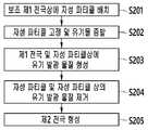
도 2는 본 발명의 일 실시예에 따른 유기 발광 표시 장치의 제조 방법을 나타내는 순서도이고, 도 3a 내지 도 3g는 본 발명의 일 실시예에 따른 유기 발광 표시 장치의 제조 방법을 나타내는 공정 단면도이다.2 is a flowchart illustrating a method of manufacturing an organic light emitting display device according to an exemplary embodiment, and FIGS. 3A to 3G are cross-sectional views illustrating a method of manufacturing an organic light emitting display device according to an exemplary embodiment.
이하, 표시 기판의 표시 영역에 박막 트랜지스터(80), 박막 트랜지스터(80)와 전기적으로 접속되는 제1 전극(220), 제1 전극(220) 상에 구비되는 유기 발광층(230), 유기 발광층(230) 상에 구비되는 제2 전극(240), 표시 기판의 비표시 영역에 형성되며, 제1 전극(220)과 동일층에 동일 물질로 형성된 보조 제1 전극(220') 및 컨택홀(92)을 통해 보조 제1 전극(220')과 전기적으로 접속되는 보조 전극(95)을 포함하는 유기 발광 표시 장치 제조 방법을 설명한다.Hereinafter, in the display area of the display substrate, the
우선, 표시 기판의 표시 영역에 게이트 전극(70), 소스 전극(50) 및 드레인 전극(60)을 포함하는 박막 트랜지스터(80)를 형성한다. 그리고, 게이트 전극(70)과 동일한 층에 상기 표시 기판의 비표시 영역에 구비되도록 보조 전극(95)을 형성한다. 그리고, 드레인 전극(60)과 전기적으로 접속되는 제1 전극(220), 및 보조 전극(5)과 전기적으로 접속되고 제1 전극(220)과는 분리되어 비표시 영역에 배치되는 보조 제1 전극(220')을 형성한다.First, a
보조 전극(95)을 박막 트랜지스터(80)의 게이트 전극(70)과 동일한 층에 형성하도록 할 수 있고, 보조 전극(95)을 소스 전극(50) 및 드레인 전극(60)과 동일한 층에 형성하도록 할 수도 있다.The
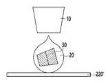
그 후, 보조 제1 전극(220') 상에 유기물(20)을 포함한 자성 파티클(30)을 배치한다(S201, 도3a).Thereafter, the
자성 파티클(30)은 액적 적하(ODF; One Drop Filling) 또는 인쇄 공법을 이용하여 보조 제1 전극(220') 상에 공급될 수 있다. 자성 파티클(30)은 유기물(20)과 혼합되어 액체 형태로 존재하며, 액적 적하 공정이라고도 하는 ODF 공정은 기판 위에 일정량의 액체를 도팅(dotting)하면서 디스펜서(dispenser)(10) 또는 스테이지(stage)를 이동시켜 일정 패턴으로 기판 등에 떨어지게 하는 방식이다. 인쇄 공법으로 예를 들어, 잉크젯 방식, 그라비아 방식, 그라비아 오프셋 방식, 스크린 프린팅 방식 등을 이용한다.The
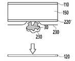
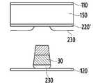
그 후, 유기물(20)을 포함한 자성 파티클(30)을 제1 전자석(110)으로 보조 제1 전극(220')에 고정시키고, 유기물(20)을 증발시킨다(S202, 도 3b 및 도 3c). 보조 제1 전극(220')은 평탄화막(150) 상에 구비되고, 평탄화막(150) 상에 제1 전자석(110)이 구비되어, 제1 전자석(110)의 자력에 의해 자성 파티클(30)을 고정시킨다. 제1 전자석(110)은 전류 인가에 의해 자성이 증폭 또는 차단될 수 있다. 또한, 제1 전자석(110)은 판상의 형태일 수 있다. 자성 파티클(30)을 함유하고 있는 유기물(20)은 열 또는 빛 등을 통해 증발시켜 자성 파티클(30)로부터 분리, 제거할 수 있다.Thereafter, the
그 후, 제1 전극(220), 보조 제1 전극(220') 및 자성 파티클(30) 상에 유기 발광 물질(230)을 형성한다(S203, 도 3d). 자성 파티클(30)과 혼합된 유기물(20)은 제거된 상태에서, 자성 파티클(30)과 제1 전극(220) 및 보조 제1 전극(220')에 동시에 유기 발광 물질(230)을 형성한다. 자성 파티클(30)은 제1 전자석(110)에 의해 보조 제1 전극(220')에 고정되어 있다.Thereafter, the organic light-emitting
그 후, 자성 파티클(30)과 소정 간격 이격된 위치에 배치되는 제2 전자석(120)을 이용하여 자성 파티클(30)을 제거한다(S204, 도 3e 및 도 3f). 제2 전자석(120)의 자력은 자성 파티클(30)을 고정하고 있는 제1 전자석(110)의 자력보다 더 크다. 자성 파티클(30)을 제2 전자석(120)에 의해 제거함으로써 자성 파티클(30) 상에 형성된 유기 발광 물질(230)도 함께 제거된다. 그 결과, 자성 파티클(30)이 고정되어 있던 보조 제1 전극(220') 부분은 유기 발광 물질(230)이 제거되어 외부로 노출된 상태가 된다.Thereafter, the
그 후, 노출된 보조 제1 전극(220') 및 유기 발광 물질(230) 상에 제2 전극(240)을 형성한다(S205, 도 3g). 이에 따라, 자성 파티클(30)이 배치되어 있다가 제거된 부분에 보조 제1 전극(220')과 제2 전극(240)이 직접 접촉되는 구조가 형성된다.Thereafter, the
도 4a 내지 도 4g는 본 발명의 다른 실시예에 따른 유기 발광 표시 장치의 제조 방법을 나타내는 공정 단면도이다.4A to 4G are cross-sectional views illustrating a method of manufacturing an organic light emitting diode display according to another exemplary embodiment.
본 실시예에서는, 앞서 살펴 본 실시예와는 달리, 자성 파티클(30)은 극성을 갖는 다각기둥 형태로 형성하고, 극성이 가변되는 전자석(110)을 이용하여 자성 파티클(30)을 보조 제1 전극(220') 상에 배치, 고정하는 점에서 상이하며 다른 구성 및 공정은 거의 동일하다. 다각기둥 형태의 자성 파티클(30)은 N극과 S극의 극성을 갖는 것일 수 있다. 즉, 다각기둥 형태의 자성 파티클(30)은 두 부분으로 나뉘어져 한 부분은 N극, 다른 부분은 S극의 성질을 가질 수 있다. 자성 파티클(30)은 무정형, 원형, 원통형, 원기둥형, 타원형, 원뿔형, 다각형 등으로 형성될 수도 있다.In this embodiment, unlike the previous embodiment, the
우선, 표시 기판의 비표시 영역의 보조 제1 전극(220') 상에 유기물(20)을 포함한 다각기둥형 자성 파티클(30)을 배치한다(도 4a). 자성 파티클(30)은 앞서 살펴 본 실시예와 마찬가지로, 액적 적하(ODF; One Drop Filling) 또는 인쇄 공법을 이용하여 제1 전극(220) 상에 공급될 수 있다.First, the polygonal columnar
그 후, 유기물(20)을 포함한 자성 파티클(30)을 제1 전자석(110)으로 보조 제1 전극(220')에 고정시킨 후, 열 또는 빛 등을 통해 유기물(20)을 증발시켜 자성 파티클(30)로부터 분리, 제거한다(도 4b). 제1 전자석(110)은 판상의 형태일 수 있고, 제2 전자석에 의해 자성 파티클(30)이 정렬된다(도 4c).Thereafter, the
그 후, 제1 전극(220), 보조 제1 전극(220') 및 자성 파티클(30) 상에 유기 발광 물질(230)을 형성하고(도 4d), 자성 파티클(30)과 소정 간격 이격된 위치에 배치되는 제2 전자석(120)을 이용하여 자성 파티클(30)과 자성 파티클(30) 상에 형성된 유기 발광 물질(230)을 제거한다(도 4e 및 도 4f).Thereafter, the organic
그 후, 노출된 보조 제1 전극(220') 및 유기 발광 물질(230) 상에 제2 전극(240)을 형성(도 4g)함으로써, 자성 파티클(30)이 배치되어 있다가 제거된 부분에서 보조 제1 전극(220')과 제2 전극(240)이 직접 접촉되는 구조가 형성된다.Thereafter, by forming the
한편, 자성 파티클(30)은, 표시 기판의 비표시 영역의 보조 제1 전극(220') 상의 하나 또는 두 개의 지점에 배치되도록 할 수 있으며, 하나 또는 그 이상의 자성 파티클(30)을 보조 제1 전극(220') 상에 배치할 수 있다.Meanwhile, the
도 5는 본 발명의 다른 실시예에 따른 자성 파티클 배치 방법을 개략적으로 나타내는 단면도이다. 본 실시예에서는, 앞서 살펴 본 두 실시예에서 판상 형태의 제1 전자석(110) 외부에 이동되도록 설치된 막대 형태의 제3 전자석(160)을 추가적으로 이용하여, 자성 파티클(30)을 보조 제1 전극(220') 상에서 이동되도록 하는 점에서, 상이하며, 이외의 공정 순서 및 구성은 동일하므로, 이하 설명은 생략한다.5 is a cross-sectional view schematically illustrating a method for disposing magnetic particles according to another embodiment of the present invention. In this embodiment, the
이와 같이, 본 발명의 실시예들에 따른 유기 발광 표시 장치 및 그 제조 방법에 의해서, 비표시 영역에 보조 전극을 형성하고, 자성 파티클을 이용하여 보조 전극을 유기 발광부의 캐소드 전극에 연결되도록 한 구조를 갖도록 하여, 캐소드의 저항을 낮출 수 있으며, 유기 발광 표시 장치의 대면적화를 실현할 수 있다.As described above, a structure in which an auxiliary electrode is formed in a non-display area and the auxiliary electrode is connected to the cathode electrode of the organic light emitting unit using magnetic particles by the organic light emitting display device and the method for manufacturing the same according to the embodiments of the present invention , it is possible to lower the resistance of the cathode and realize a large area of the organic light emitting display device.
본 발명을 앞서 기재한 바에 따라 바람직한 실시예를 통해 설명하였지만, 본 발명은 이에 한정되지 않으며 다음에 기재하는 특허청구범위의 개념과 범위를 벗어나지 않는 한, 다양한 수정 및 변형이 가능하다는 것을 본 발명이 속하는 기술 분야에 종사하는 자들은 쉽게 이해할 것이다.Although the present invention has been described through preferred embodiments as described above, the present invention is not limited thereto, and various modifications and variations are possible without departing from the concept and scope of the following claims. Those in the technical field to which it belongs will readily understand.
10: 디스펜서(dispenser)20: 유기물
30: 자성 파티클40, 90: 반도체층
50: 소스 전극60: 드레인 전극
70: 게이트 전극 80: 박막 트랜지스터
92: 컨택홀95: 보조 전극
110: 제1 전자석120: 제2 전자석
160: 제3 전자석 130: 게이트 절연막
140: 층간 절연막150: 평탄화막
200: 유기 발광 소자220: 제1 전극
230: 유기 발광층(유기 발광 물질)240: 제2 전극
310: 화소 정의막10: dispenser 20: organic matter
30: magnetic particles 40, 90: semiconductor layer
50: source electrode 60: drain electrode
70: gate electrode 80: thin film transistor
92: contact hole 95: auxiliary electrode
110: first electromagnet 120: second electromagnet
160: third electromagnet 130: gate insulating film
140: interlayer insulating film 150: planarization film
200: organic light emitting device 220: first electrode
230: organic light emitting layer (organic light emitting material) 240: second electrode
310: pixel defining layer
Claims (16)
Translated fromKorean상기 표시 기판의 비표시 영역에 구비되도록 보조 전극을 형성하는 단계;
상기 드레인 전극과 전기적으로 접속되는 제1 전극, 및 상기 보조 전극과 전기적으로 접속되고 상기 제1 전극과 동일층에 동일 물질로 형성되며, 상기 제1 전극과 분리되어 상기 비표시 영역에 배치되는 보조 제1 전극을 형성하는 단계;
상기 보조 제1 전극 상에 유기물을 포함한 자성 파티클을 배치하는 자성 파티클 배치 단계:
상기 유기물을 포함한 자성 파티클을 제1 전자석으로 상기 보조 제1 전극에 고정시키고, 상기 유기물을 증발시키는 유기물 증발 단계;
상기 제1 전극 및 상기 자성 파티클 상에 유기 발광 물질을 형성하는 유기 발광 물질 형성 단계;
상기 자성 파티클과 이격된 위치에 배치되는 제2 전자석을 이용하여 상기 자성 파티클 및 상기 자성 파티클 상에 형성된 유기 발광 물질을 제거하는 자성 파티클 및 유기 발광 물질 제거 단계; 및
상기 보조 제1 전극 및 상기 유기 발광 물질 상에 제2 전극을 형성하는 제2 전극 형성 단계를 포함하는 유기 발광 표시 장치 제조 방법.forming a thin film transistor including a gate electrode, a source electrode, and a drain electrode in a display area of a display substrate;
forming an auxiliary electrode to be provided in a non-display area of the display substrate;
A first electrode electrically connected to the drain electrode, and an auxiliary electrode electrically connected to the auxiliary electrode and formed of the same material on the same layer as the first electrode, separated from the first electrode and disposed in the non-display area forming a first electrode;
A magnetic particle arrangement step of disposing magnetic particles including an organic material on the auxiliary first electrode:
an organic material evaporation step of fixing the magnetic particles including the organic material to the auxiliary first electrode with a first electromagnet and evaporating the organic material;
an organic light emitting material forming step of forming an organic light emitting material on the first electrode and the magnetic particles;
removing the magnetic particles and the organic light emitting material formed on the magnetic particles and the organic light emitting material by using a second electromagnet that is spaced apart from the magnetic particles; and
and a second electrode forming step of forming a second electrode on the auxiliary first electrode and the organic light emitting material.
상기 제2 전극 형성 단계는,
상기 보조 제1 전극이 상기 제2 전극과 접촉하도록 하는 유기 발광 표시 장치 제조 방법.In claim 1,
The second electrode forming step,
A method of manufacturing an organic light emitting diode display such that the auxiliary first electrode contacts the second electrode.
상기 보조 전극 형성 단계는,
상기 보조 전극을 상기 게이트 전극과 동일한 층에 형성하도록 하는 유기 발광 표시 장치 제조 방법.In claim 1,
The auxiliary electrode forming step is
and forming the auxiliary electrode on the same layer as the gate electrode.
상기 보조 전극 형성 단계는,
상기 보조 전극을 상기 소스 전극 및 상기 드레인 전극과 동일한 층에 형성하도록 하는 유기 발광 표시 장치 제조 방법.In claim 1,
The auxiliary electrode forming step is
and forming the auxiliary electrode on the same layer as the source electrode and the drain electrode.
상기 자성 파티클 배치 단계는,
상기 자성 파티클을 액적 적하(ODF; One Drop Filling) 또는 인쇄 공법을 이용하여 상기 제1 전극 상에 공급하는 유기 발광 표시 장치 제조 방법.In claim 1,
The magnetic particle arrangement step is,
A method of manufacturing an organic light emitting display device in which the magnetic particles are supplied onto the first electrode by using one drop filling (ODF) or a printing method.
상기 자성 파티클 배치 단계는,
무정형, 원형, 원통형, 원기둥형, 타원형, 원뿔형, 다각형, 다각기둥 중 어느 하나의 형태의 자성 파티클을 이용하는 유기 발광 표시 장치 제조 방법.In claim 1,
The magnetic particle arrangement step is,
A method of manufacturing an organic light emitting display device using magnetic particles having any one of amorphous, circular, cylindrical, cylindrical, elliptical, conical, polygonal, and polygonal shapes.
상기 자성 파티클 배치 단계는,
상기 보조 제1 전극 상의 하나 또는 두 개의 지점에 배치되도록 하는 유기 발광 표시 장치 제조 방법.In claim 1,
The magnetic particle arrangement step is,
A method of manufacturing an organic light emitting display device to be disposed at one or two points on the auxiliary first electrode.
상기 자성 파티클 배치 단계는,
하나 또는 그 이상의 자성 파티클을 상기 보조 제1 전극 상에 배치하는 유기 발광 표시 장치 제조 방법.In claim 1,
The magnetic particle arrangement step is,
A method of manufacturing an organic light emitting diode display for disposing one or more magnetic particles on the auxiliary first electrode.
상기 자성 파티클 배치 단계는,
극성을 가지는 자성 파티클을 상기 보조 제1 전극 상에 배치하는 유기 발광 표시 장치 제조 방법.In claim 1,
The magnetic particle arrangement step is,
A method of manufacturing an organic light emitting diode display for disposing a magnetic particle having a polarity on the auxiliary first electrode.
상기 유기물 증발 단계는,
극성이 가변되는 상기 제1 전자석을 이용하여 상기 유기물을 포함한 자성 파티클을 상기 보조 제1 전극에 고정시키는 유기 발광 표시 장치 제조 방법.In claim 1,
The organic material evaporation step,
A method of manufacturing an organic light emitting display device for fixing the magnetic particles including the organic material to the auxiliary first electrode using the first electromagnet having a variable polarity.
상기 유기물 증발 단계는,
자성을 증폭 또는 차단시킬 수 있는 상기 제1 전자석을 이용하여 상기 유기물을 포함한 자성 파티클을 상기 보조 제1 전극에 고정시키는 유기 발광 표시 장치 제조 방법.In claim 1,
The organic material evaporation step,
A method of manufacturing an organic light emitting display device in which the magnetic particles including the organic material are fixed to the auxiliary first electrode by using the first electromagnet capable of amplifying or blocking magnetism.
상기 유기물 증발 단계는,
판상의 상기 제1 전자석을 이용하여 상기 유기물을 포함한 자성 파티클을 상기 보조 제1 전극에 고정시키는 유기 발광 표시 장치 제조 방법.In claim 1,
The organic material evaporation step,
A method of manufacturing an organic light emitting display device for fixing the magnetic particles including the organic material to the auxiliary first electrode using the plate-shaped first electromagnet.
상기 유기물 증발 단계는,
이동되도록 설치된 막대 형태의 제3 전자석을 이용하여 상기 자성 파티클을 상기 보조 제1 전극 상에서 이동되도록 하는 유기 발광 표시 장치 제조 방법.In claim 1,
The organic material evaporation step,
A method of manufacturing an organic light emitting display device, wherein the magnetic particles are moved on the auxiliary first electrode by using a third electromagnet in the form of a rod installed to be moved.
Priority Applications (2)
| Application Number | Priority Date | Filing Date | Title |
|---|---|---|---|
| KR1020150029334AKR102449258B1 (en) | 2015-03-02 | 2015-03-02 | Organic light emitting display device and manufacturing method thereof |
| US15/000,956US9786867B2 (en) | 2015-03-02 | 2016-01-19 | Method of manufacturing an organic light emitting display including a magnetic particle on a first electrode |
Applications Claiming Priority (1)
| Application Number | Priority Date | Filing Date | Title |
|---|---|---|---|
| KR1020150029334AKR102449258B1 (en) | 2015-03-02 | 2015-03-02 | Organic light emitting display device and manufacturing method thereof |
Publications (2)
| Publication Number | Publication Date |
|---|---|
| KR20160106847A KR20160106847A (en) | 2016-09-13 |
| KR102449258B1true KR102449258B1 (en) | 2022-09-29 |
Family
ID=56850796
Family Applications (1)
| Application Number | Title | Priority Date | Filing Date |
|---|---|---|---|
| KR1020150029334AActiveKR102449258B1 (en) | 2015-03-02 | 2015-03-02 | Organic light emitting display device and manufacturing method thereof |
Country Status (2)
| Country | Link |
|---|---|
| US (1) | US9786867B2 (en) |
| KR (1) | KR102449258B1 (en) |
Families Citing this family (5)
| Publication number | Priority date | Publication date | Assignee | Title |
|---|---|---|---|---|
| KR102627284B1 (en)* | 2016-05-12 | 2024-01-22 | 엘지디스플레이 주식회사 | Method of manufacturing a connection structure connecting cathode electrode to auxiliary cathode electrode, and organic light emitting diode display device using the same |
| CN107394062B (en)* | 2017-07-20 | 2019-02-05 | 京东方科技集团股份有限公司 | An organic light emitting diode display panel, a method for making the same, and a display device |
| CN110828518B (en)* | 2019-11-15 | 2022-06-21 | 京东方科技集团股份有限公司 | Display device, display panel and manufacturing method thereof |
| CN111403622B (en)* | 2020-03-26 | 2023-04-07 | 京东方科技集团股份有限公司 | OLED display panel, manufacturing method thereof and display device |
| KR102740672B1 (en) | 2021-10-20 | 2024-12-11 | 한양대학교 에리카산학협력단 | SNP marker composition for diagnosis of volatile organic compounds-induced atopic dermatitis |
Family Cites Families (10)
| Publication number | Priority date | Publication date | Assignee | Title |
|---|---|---|---|---|
| JP2009302025A (en) | 2008-06-17 | 2009-12-24 | Seiko Epson Corp | Organic light-emitting device and electronic equipment |
| KR101460653B1 (en) | 2008-07-23 | 2014-11-12 | 삼성디스플레이 주식회사 | Organic light emitting display and method of manufacuring the same |
| KR101574211B1 (en)* | 2008-09-05 | 2015-12-07 | 삼성디스플레이 주식회사 | Organic light emitting diode display |
| JP5157825B2 (en)* | 2008-10-29 | 2013-03-06 | ソニー株式会社 | Manufacturing method of organic EL display |
| KR101672908B1 (en) | 2008-11-07 | 2016-11-07 | 엘지디스플레이 주식회사 | Top emission type organic Electroluminescent Device |
| KR20110019498A (en)* | 2009-08-20 | 2011-02-28 | 삼성모바일디스플레이주식회사 | Organic light emitting display |
| US20130056784A1 (en)* | 2011-09-02 | 2013-03-07 | Lg Display Co., Ltd. | Organic Light-Emitting Display Device and Method of Fabricating the Same |
| KR101901574B1 (en) | 2011-12-21 | 2018-09-28 | 엘지디스플레이 주식회사 | Organic light emitting display device and method for fabricating the same |
| KR20140067645A (en)* | 2012-11-27 | 2014-06-05 | 엘지디스플레이 주식회사 | Organic electro-luminescent device and method of fabricating the same |
| KR101560272B1 (en)* | 2013-02-25 | 2015-10-15 | 삼성디스플레이 주식회사 | Organic light emitting display device and manufacturing method of the same |
- 2015
- 2015-03-02KRKR1020150029334Apatent/KR102449258B1/enactiveActive
- 2016
- 2016-01-19USUS15/000,956patent/US9786867B2/enactiveActive
Also Published As
| Publication number | Publication date |
|---|---|
| US9786867B2 (en) | 2017-10-10 |
| US20160260922A1 (en) | 2016-09-08 |
| KR20160106847A (en) | 2016-09-13 |
Similar Documents
| Publication | Publication Date | Title |
|---|---|---|
| US8587499B2 (en) | Organic light emitting diode display | |
| KR102180037B1 (en) | Flexible display and manufacturing method thereof | |
| CN110581158B (en) | Organic light emitting display device and method of manufacturing the same | |
| US8188509B2 (en) | Organic light emitting display device | |
| KR101378439B1 (en) | Organic light emitting diode display and method for manufacturing the same | |
| KR100989133B1 (en) | Organic light emitting display | |
| KR20240017893A (en) | Organic luminescence emitting display device and method for manufacturing the same | |
| KR102161600B1 (en) | Organic light emitting display and manufacturing method thereof | |
| KR102280959B1 (en) | Display device and method for manufacturing the same | |
| TW201633529A (en) | Organic light emitting display device | |
| KR102449258B1 (en) | Organic light emitting display device and manufacturing method thereof | |
| US9595694B2 (en) | Thin film transistor substrate, organic light-emitting apparatus including the same, method of manufacturing the thin film transistor substrate, and method of manufacturing the organic light-emitting apparatus | |
| KR20150046646A (en) | Organic light-emitting display apparatus | |
| KR20120042068A (en) | Organic light emitting diode display | |
| US20160260924A1 (en) | Organic light emitting diode display and method of manufacturng the same | |
| US20200020880A1 (en) | Display device | |
| CN106098730B (en) | Organic light emitting device and method of manufacturing the same | |
| CN106067474A (en) | Organic light-emitting display device | |
| JP2011258945A (en) | Organic light-emitting display device and method for manufacturing the same | |
| KR20140140960A (en) | Organic light emitting diode display | |
| KR20140046519A (en) | Organic light emitting diode display | |
| KR101899477B1 (en) | Thin film transistor, method for manufacturing the same and the organic light emitting diode display comprising the same | |
| KR102296915B1 (en) | organic light emitting diode display | |
| KR102205859B1 (en) | Display device and method for manufacturing the same | |
| US10991910B2 (en) | Display device and production method therefor |
Legal Events
| Date | Code | Title | Description |
|---|---|---|---|
| PA0109 | Patent application | Patent event code:PA01091R01D Comment text:Patent Application Patent event date:20150302 | |
| PG1501 | Laying open of application | ||
| A201 | Request for examination | ||
| PA0201 | Request for examination | Patent event code:PA02012R01D Patent event date:20200224 Comment text:Request for Examination of Application Patent event code:PA02011R01I Patent event date:20150302 Comment text:Patent Application | |
| E902 | Notification of reason for refusal | ||
| PE0902 | Notice of grounds for rejection | Comment text:Notification of reason for refusal Patent event date:20210628 Patent event code:PE09021S01D | |
| E90F | Notification of reason for final refusal | ||
| PE0902 | Notice of grounds for rejection | Comment text:Final Notice of Reason for Refusal Patent event date:20220102 Patent event code:PE09021S02D | |
| E701 | Decision to grant or registration of patent right | ||
| PE0701 | Decision of registration | Patent event code:PE07011S01D Comment text:Decision to Grant Registration Patent event date:20220706 | |
| GRNT | Written decision to grant | ||
| PR0701 | Registration of establishment | Comment text:Registration of Establishment Patent event date:20220926 Patent event code:PR07011E01D | |
| PR1002 | Payment of registration fee | Payment date:20220926 End annual number:3 Start annual number:1 | |
| PG1601 | Publication of registration |