KR102448483B1 - Thin film transistor substrate having high mobility semiconductor material and method for manufacturing the same - Google Patents
Thin film transistor substrate having high mobility semiconductor material and method for manufacturing the sameDownload PDFInfo
- Publication number
- KR102448483B1 KR102448483B1KR1020170081022AKR20170081022AKR102448483B1KR 102448483 B1KR102448483 B1KR 102448483B1KR 1020170081022 AKR1020170081022 AKR 1020170081022AKR 20170081022 AKR20170081022 AKR 20170081022AKR 102448483 B1KR102448483 B1KR 102448483B1
- Authority
- KR
- South Korea
- Prior art keywords
- oxide semiconductor
- semiconductor layer
- thin film
- film transistor
- oxygen
- Prior art date
- Legal status (The legal status is an assumption and is not a legal conclusion. Google has not performed a legal analysis and makes no representation as to the accuracy of the status listed.)
- Active
Links
Images


Classifications
- H—ELECTRICITY
- H10—SEMICONDUCTOR DEVICES; ELECTRIC SOLID-STATE DEVICES NOT OTHERWISE PROVIDED FOR
- H10D—INORGANIC ELECTRIC SEMICONDUCTOR DEVICES
- H10D30/00—Field-effect transistors [FET]
- H10D30/60—Insulated-gate field-effect transistors [IGFET]
- H10D30/67—Thin-film transistors [TFT]
- H10D30/674—Thin-film transistors [TFT] characterised by the active materials
- H10D30/6755—Oxide semiconductors, e.g. zinc oxide, copper aluminium oxide or cadmium stannate
- H01L29/7869—
- H—ELECTRICITY
- H01—ELECTRIC ELEMENTS
- H01L—SEMICONDUCTOR DEVICES NOT COVERED BY CLASS H10
- H01L21/00—Processes or apparatus adapted for the manufacture or treatment of semiconductor or solid state devices or of parts thereof
- H01L21/02—Manufacture or treatment of semiconductor devices or of parts thereof
- H01L21/02104—Forming layers
- H01L21/02107—Forming insulating materials on a substrate
- H01L21/02225—Forming insulating materials on a substrate characterised by the process for the formation of the insulating layer
- H01L21/0226—Forming insulating materials on a substrate characterised by the process for the formation of the insulating layer formation by a deposition process
- H01L21/02263—Forming insulating materials on a substrate characterised by the process for the formation of the insulating layer formation by a deposition process deposition from the gas or vapour phase
- H01L21/02271—Forming insulating materials on a substrate characterised by the process for the formation of the insulating layer formation by a deposition process deposition from the gas or vapour phase deposition by decomposition or reaction of gaseous or vapour phase compounds, i.e. chemical vapour deposition
- H01L21/02274—Forming insulating materials on a substrate characterised by the process for the formation of the insulating layer formation by a deposition process deposition from the gas or vapour phase deposition by decomposition or reaction of gaseous or vapour phase compounds, i.e. chemical vapour deposition in the presence of a plasma [PECVD]
- H—ELECTRICITY
- H01—ELECTRIC ELEMENTS
- H01L—SEMICONDUCTOR DEVICES NOT COVERED BY CLASS H10
- H01L21/00—Processes or apparatus adapted for the manufacture or treatment of semiconductor or solid state devices or of parts thereof
- H01L21/02—Manufacture or treatment of semiconductor devices or of parts thereof
- H01L21/04—Manufacture or treatment of semiconductor devices or of parts thereof the devices having potential barriers, e.g. a PN junction, depletion layer or carrier concentration layer
- H01L21/18—Manufacture or treatment of semiconductor devices or of parts thereof the devices having potential barriers, e.g. a PN junction, depletion layer or carrier concentration layer the devices having semiconductor bodies comprising elements of Group IV of the Periodic Table or AIIIBV compounds with or without impurities, e.g. doping materials
- H01L21/30—Treatment of semiconductor bodies using processes or apparatus not provided for in groups H01L21/20 - H01L21/26
- H01L21/324—Thermal treatment for modifying the properties of semiconductor bodies, e.g. annealing, sintering
- H01L29/778—
- H01L29/78618—
- H—ELECTRICITY
- H10—SEMICONDUCTOR DEVICES; ELECTRIC SOLID-STATE DEVICES NOT OTHERWISE PROVIDED FOR
- H10D—INORGANIC ELECTRIC SEMICONDUCTOR DEVICES
- H10D30/00—Field-effect transistors [FET]
- H10D30/40—FETs having zero-dimensional [0D], one-dimensional [1D] or two-dimensional [2D] charge carrier gas channels
- H10D30/47—FETs having zero-dimensional [0D], one-dimensional [1D] or two-dimensional [2D] charge carrier gas channels having 2D charge carrier gas channels, e.g. nanoribbon FETs or high electron mobility transistors [HEMT]
- H—ELECTRICITY
- H10—SEMICONDUCTOR DEVICES; ELECTRIC SOLID-STATE DEVICES NOT OTHERWISE PROVIDED FOR
- H10D—INORGANIC ELECTRIC SEMICONDUCTOR DEVICES
- H10D30/00—Field-effect transistors [FET]
- H10D30/60—Insulated-gate field-effect transistors [IGFET]
- H10D30/67—Thin-film transistors [TFT]
- H10D30/6704—Thin-film transistors [TFT] having supplementary regions or layers in the thin films or in the insulated bulk substrates for controlling properties of the device
- H10D30/6713—Thin-film transistors [TFT] having supplementary regions or layers in the thin films or in the insulated bulk substrates for controlling properties of the device characterised by the properties of the source or drain regions, e.g. compositions or sectional shapes
Landscapes
- Engineering & Computer Science (AREA)
- Physics & Mathematics (AREA)
- Condensed Matter Physics & Semiconductors (AREA)
- General Physics & Mathematics (AREA)
- Manufacturing & Machinery (AREA)
- Computer Hardware Design (AREA)
- Microelectronics & Electronic Packaging (AREA)
- Power Engineering (AREA)
- Plasma & Fusion (AREA)
- Chemical & Material Sciences (AREA)
- Chemical Kinetics & Catalysis (AREA)
- Thin Film Transistor (AREA)
Abstract
Translated fromKoreanDescription
Translated fromKorean본 발명은 산화물 반도체 물질을 구비한 박막 트랜지스터 기판 및 그 제조 방법에 관한 것이다. 특히, 본 발명은 고 이동도 특성과 높은 신뢰성을 갖는 산화물 반도체 물질을 구비한 박막 트랜지스터 기판 및 그 제조 방법에 관한 것이다.The present invention relates to a thin film transistor substrate having an oxide semiconductor material and a method for manufacturing the same. In particular, the present invention relates to a thin film transistor substrate having an oxide semiconductor material having high mobility characteristics and high reliability, and a method for manufacturing the same.
표시장치 분야는 부피가 큰 음극선관(Cathode Ray Tube: CRT)을 대체하는, 얇고 가벼우며 대면적이 가능한 평판 표시장치(Flat Panel Display Device: FPD)로 급속히 변화해 왔다. 평판 표시장치에는 액정 표시장치(Liquid Crystal Display Device: LCD), 플라즈마 디스플레이 패널(Plasma Display Panel: PDP), 유기발광 표시장치(Organic Light Emitting Display Device: OLED), 그리고 전기영동 표시장치(Electrophoretic Display Device: ED) 등이 있다.The display device field has rapidly changed to a thin, light, and large-area Flat Panel Display Device (FPD) that replaces a bulky cathode ray tube (CRT). Flat panel displays include Liquid Crystal Display Device (LCD), Plasma Display Panel (PDP), Organic Light Emitting Display Device (OLED), and Electrophoretic Display Device. : ED), etc.
능동형으로 구동하는 액정 표시장치, 유기발광 표시장치 및 전기영동 표시장치의 경우, 매트릭스 방식으로 배열된 화소 영역 내에 할당된 박막 트랜지스터가 배치된 박막 트랜지스터 기판을 포함한다. 액정 표시장치(Liquid Crystal Display Device: LCD)는 전계를 이용하여 액정의 광 투과율을 조절함으로써 화상을 표시한다. 유기발광 표시장치는 매트릭스 방식으로 배열된 화소 자체에 유기발광 소자를 형성함으로써, 화상을 표시한다.In the case of a liquid crystal display device, an organic light emitting display device, and an electrophoretic display device that are actively driven, a thin film transistor substrate is included in which thin film transistors allocated in pixel regions arranged in a matrix manner are disposed. A liquid crystal display device (LCD) displays an image by controlling the light transmittance of liquid crystal using an electric field. An organic light emitting display device displays an image by forming an organic light emitting element in pixels arranged in a matrix manner.
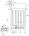
도 1은 종래 기술에 의한 수평 전계형의 일종인 프린지 필드 방식의 액정 표시장치에 포함된 산화물 반도체 층을 갖는 박막 트랜지스터 기판을 나타내는 평면도이다. 도 2는 도 1에 도시한 박막 트랜지스터 기판을 절취선 I-I' 선을 따라 자른 단면도이다.1 is a plan view illustrating a thin film transistor substrate having an oxide semiconductor layer included in a fringe field type liquid crystal display, which is a type of horizontal electric field type according to the prior art. FIG. 2 is a cross-sectional view of the thin film transistor substrate shown in FIG. 1 taken along the perforated line I-I'.
도 1 및 도 2에 도시된 금속 산화물 반도체 층을 갖는 박막 트랜지스터 기판은 하부 기판(SUB) 위에 게이트 절연막(GI)을 사이에 두고 교차하는 게이트 배선(GL) 및 데이터 배선(DL), 그 교차 구조에 의해 정의된 각 화소 영역 내에 형성된 박막 트랜지스터(T)를 구비한다.The thin film transistor substrate having the metal oxide semiconductor layer shown in FIGS. 1 and 2 includes a gate line GL and a data line DL crossing a lower substrate SUB with a gate insulating layer GI interposed therebetween, and a structure thereof. and a thin film transistor T formed in each pixel area defined by .
박막 트랜지스터(T)는 게이트 배선(GL)에서 분기한 게이트 전극(G), 데이터 배선(DL)에서 분기된 소스 전극(S), 소스 전극(S)과 대향하는 드레인 전극(D), 그리고 게이트 절연막(GI) 위에서 게이트 전극(G)과 중첩하면 소스 전극(S)과 드레인 전극(D) 사이에 채널 영역을 형성하는 반도체 층(A)을 포함한다.The thin film transistor T includes a gate electrode G branched from the gate line GL, a source electrode S branched from the data line DL, a drain electrode D facing the source electrode S, and a gate A semiconductor layer (A) that forms a channel region between the source electrode (S) and the drain electrode (D) when overlapping the gate electrode (G) on the insulating layer (GI) is included.
특히, 반도체 층(A)을 산화물 반도체 물질로 형성하는 경우, 높은 전하 이동도 특성에 의해 충전 용량이 큰 대면적 박막 트랜지스터 기판에 유리하다. 그러나 산화물 반도체 물질은 소자의 안정성을 확보하기 위해 상부 표면에 식각액으로부터 보호를 위한 에치 스토퍼(ES)를 더 포함하는 것이 바람직하다. 구체적으로, 소스 전극(S)과 드레인 전극(D) 사이의 분리된 부분을 통해 유입되는 식각액으로부터 반도체 층(A)을 보호하도록 에치 스토퍼(ES)를 형성하는 것이 바람직하다.In particular, when the semiconductor layer (A) is formed of an oxide semiconductor material, it is advantageous for a large-area thin film transistor substrate having a large charge capacity due to high charge mobility. However, it is preferable that the oxide semiconductor material further include an etch stopper (ES) on the upper surface for protection from an etchant in order to secure device stability. Specifically, it is preferable to form the etch stopper ES to protect the semiconductor layer A from the etchant flowing through the separated portion between the source electrode S and the drain electrode D.
게이트 배선(GL)의 일측 단부에는 외부로부터 게이트 신호를 인가받기 위한 게이트 패드(GP)를 포함한다. 게이트 패드(GP)는 게이트 절연막(GI)을 관통하는 제1 게이트 패드 콘택홀(GH1)을 통해 게이트 패드 중간 단자(IGT)와 접촉한다. 게이트 패드 중간 단자(IGT)는 제1 보호막(PA1)과 제2 보호막(PA2)을 관통하는 제2 게이트 패드 콘택홀(GH2)을 통해 게이트 패드 단자(GPT)와 접촉한다. 한편, 데이터 배선(DL)의 일측 단부에는 외부로부터 화소 신호를 인가받기 위한 데이터 패드(DP)를 포함한다. 데이터 패드(DP)는 제1 보호막(PA1) 및 제2 보호막(PA2)을 관통하는 데이터 패드 콘택홀(DPH)을 통해 데이터 패드 단자(DPT)와 접촉한다.A gate pad GP for receiving a gate signal from the outside is included at one end of the gate line GL. The gate pad GP contacts the gate pad intermediate terminal IGT through the first gate pad contact hole GH1 penetrating the gate insulating layer GI. The gate pad intermediate terminal IGT contacts the gate pad terminal GPT through the second gate pad contact hole GH2 penetrating the first passivation layer PA1 and the second passivation layer PA2 . Meanwhile, one end of the data line DL includes a data pad DP for receiving a pixel signal from the outside. The data pad DP contacts the data pad terminal DPT through the data pad contact hole DPH penetrating the first passivation layer PA1 and the second passivation layer PA2 .
화소 영역에는 프린지 필드를 형성하도록 제2 보호막(PA2)을 사이에 두고 형성된 화소 전극(PXL)과 공통 전극(COM)을 구비한다. 공통 전극(COM)은 게이트 배선(GL)과 나란하게 배열된 공통 배선(CL)과 접속된다. 공통 전극(COM)은 공통 배선(CL)을 통해 액정 구동을 위한 기준 전압(혹은 공통 전압)을 공급받는다.In the pixel area, the pixel electrode PXL and the common electrode COM are provided with the second passivation layer PA2 interposed therebetween to form a fringe field. The common electrode COM is connected to the common line CL arranged in parallel with the gate line GL. The common electrode COM receives a reference voltage (or a common voltage) for driving the liquid crystal through the common line CL.
공통 전극(COM)과 화소 전극(PXL)의 위치 및 모양은 설계 환경과 목적에 맞추어 다양하게 형성할 수 있다. 공통 전극(COM)은 일정한 기준 전압이 인가되는 반면, 화소 전극(PXL)은 구현하고자 하는 비디오 데이터에 따라 수시로 변화하는 전압 값이 인가된다. 따라서, 데이터 배선(DL)과 화소 전극(PXL) 사이에 기생 용량이 발생할 수 있다. 이러한 기생 용량으로 인해 화질에 문제를 야기할 수 있기 때문에, 공통 전극(COM)을 먼저 형성하고, 화소 전극(PXL)을 최상위층에 형성하는 것이 바람직하다.The positions and shapes of the common electrode COM and the pixel electrode PXL may be formed in various ways according to the design environment and purpose. A constant reference voltage is applied to the common electrode COM, while a voltage value that changes frequently according to video data to be implemented is applied to the pixel electrode PXL. Accordingly, a parasitic capacitance may be generated between the data line DL and the pixel electrode PXL. Since such a parasitic capacitance may cause a problem in image quality, it is preferable to first form the common electrode COM and then form the pixel electrode PXL on the uppermost layer.
즉, 데이터 배선(DL) 및 박막 트랜지스터(T)를 덮는 제1 보호막(PA1) 위에 유전율이 낮은 유기물질을 두껍게 형성한 평탄화 막(PAC)을 형성한 후에, 공통 전극(COM) 형성한다. 그리고 공통 전극(COM)을 덮는 제2 보호막(PA2)을 형성한 후, 공통 전극(COM)과 중첩하는 화소 전극(PXL)을 제2 보호막(PA2) 위에 형성한다. 이러한 구조에서는 화소 전극(PXL)이 데이터 배선(DL)과 제1 보호막(PA1), 평탄화 막(PAC), 그리고 제2 보호막(PA2)에 의해 이격되므로 데이터 배선(DL)과 화소 전극(PXL) 사이에 기생 용량을 줄일 수 있다.That is, after forming the planarization layer PAC in which an organic material having a low dielectric constant is thickly formed on the first passivation layer PA1 covering the data line DL and the thin film transistor T, the common electrode COM is formed. Then, after the second passivation layer PA2 covering the common electrode COM is formed, the pixel electrode PXL overlapping the common electrode COM is formed on the second passivation layer PA2 . In this structure, since the pixel electrode PXL is spaced apart by the data line DL, the first passivation layer PA1, the planarization layer PAC, and the second passivation layer PA2, the data line DL and the pixel electrode PXL It is possible to reduce the parasitic capacity in between.
공통 전극(COM)은 화소 영역의 형태에 대응하는 장방형으로 형성되고, 화소 전극(PXL)은 다수 개의 선분 형상으로 형성된다. 특히, 화소 전극(PXL)은 제2 보호막(PA2)을 사이에 두고 공통 전극(COM)과 수직 상으로 중첩하는 구조를 갖는다. 화소 전극(PXL)과 공통 전극(COM) 사이에서 프린지 필드가 형성되어 박막 트랜지스터 기판과 컬러 필터 기판 사이에서 수평 방향으로 배열된 액정분자들이 유전 이방성에 의해 회전한다. 그리고 액정 분자들의 회전 정도에 따라 화소 영역을 투과하는 광 투과율이 달라져 계조를 구현한다.The common electrode COM is formed in a rectangular shape corresponding to the shape of the pixel area, and the pixel electrode PXL is formed in the shape of a plurality of line segments. In particular, the pixel electrode PXL has a structure that vertically overlaps the common electrode COM with the second passivation layer PA2 interposed therebetween. A fringe field is formed between the pixel electrode PXL and the common electrode COM, so that liquid crystal molecules arranged in a horizontal direction between the thin film transistor substrate and the color filter substrate rotate due to dielectric anisotropy. In addition, the light transmittance through the pixel region varies according to the degree of rotation of the liquid crystal molecules to realize grayscale.
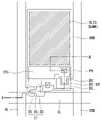
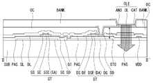
다른 평판표시장치의 예로, 전계발광 표시장치가 있다. 전계발광 표시장치는 발광 층의 재료에 따라 무기 전계발광 표시장치와 유기발광 다이오드 표시장치로 대별되며, 스스로 발광하는 자발광 소자로서 응답속도가 빠르고 발광효율, 휘도 및 시야각이 큰 장점이 있다. 특히, 에너지 효율이 우수한 유기발광 다이오드의 특징을 이용한 유기발광 다이오드 표시장치(Organic Light Emitting Diode display: OLEDD)에는 패시브 매트릭스 타입의 유기발광 다이오드 표시장치(Passive Matrix type Organic Light Emitting Diode display, PMOLED)와 액티브 매트릭스 타입의 유기발광 다이오드 표시장치(Active Matrix type Organic Light Emitting Diode display, AMOLED)로 대별된다.An example of another flat panel display device is an electroluminescence display device. The electroluminescent display device is broadly classified into an inorganic electroluminescent display device and an organic light emitting diode display device according to the material of the light emitting layer. In particular, in an organic light emitting diode display (OLED) using the characteristics of an organic light emitting diode having excellent energy efficiency, a passive matrix type organic light emitting diode display (PMOLED) and It is roughly classified into an active matrix type organic light emitting diode display (AMOLED).
도 3은 액티브 매트릭스 유기발광 다이오드 표시장치에서 한 화소의 구조를 나타내는 평면도이다. 도 4는 도 3에서 절취선 II-II'로 자른 액티브 매트릭스 유기발광 다이오드 표시장치의 구조를 나타내는 단면도이다.3 is a plan view illustrating a structure of one pixel in an active matrix organic light emitting diode display device. FIG. 4 is a cross-sectional view showing the structure of the active matrix organic light emitting diode display device taken along the cut line II-II' in FIG. 3 .
도 3 및 4를 참조하면, 액티브 매트릭스 유기발광 다이오드 표시장치는 스위칭 박막 트랜지스터(ST), 스위칭 박막 트랜지스터와 연결된 구동 박막 트랜지스터(DT), 구동 박막 트랜지스터(DT)에 접속된 유기발광 다이오드(OLE)를 포함한다.3 and 4 , the active matrix organic light emitting diode display includes a switching thin film transistor ST, a driving thin film transistor DT connected to the switching thin film transistor, and an organic light emitting diode OLE connected to the driving thin film transistor DT. includes
스위칭 박막 트랜지스터(ST)는 스캔 배선(SL)과 데이터 배선(DL)이 교차하는 부위에 형성되어 있다. 스위칭 박막 트랜지스터(ST)는 화소를 선택하는 기능을 한다. 스위칭 박막 트랜지스터(ST)는 스캔 배선(SL)에서 분기하는 게이트 전극(SG)과, 반도체 층(SA)과, 소스 전극(SS)과, 드레인 전극(SD)을 포함한다. 그리고 구동 박막 트랜지스터(DT)는 스위칭 박막 트랜지스터(ST)에 의해 선택된 화소의 유기발광 다이오드(OLE)를 구동하는 역할을 한다.The switching thin film transistor ST is formed at the intersection of the scan line SL and the data line DL. The switching thin film transistor ST functions to select a pixel. The switching thin film transistor ST includes a gate electrode SG branching from the scan line SL, a semiconductor layer SA, a source electrode SS, and a drain electrode SD. In addition, the driving thin film transistor DT serves to drive the organic light emitting diode OLE of the pixel selected by the switching thin film transistor ST.
구동 박막 트랜지스터(DT)는 스위칭 박막 트랜지스터(ST)의 드레인 전극(SD)과 연결된 게이트 전극(DG)과, 반도체 층(DA), 구동 전류 배선(VDD)에 연결된 소스 전극(DS)과, 드레인 전극(DD)을 포함한다. 구동 박막 트랜지스터(DT)의 드레인 전극(DD)은 유기발광 다이오드(OLE)의 애노드 전극(ANO)과 연결되어 있다. 애노드 전극(ANO)과 캐소드 전극(CAT) 사이에는 유기발광 층(OL)이 개재되어 있다. 캐소드 전극(CAT)은 기저 전압(VSS)에 연결된다.The driving thin film transistor DT has a gate electrode DG connected to the drain electrode SD of the switching thin film transistor ST, a semiconductor layer DA, a source electrode DS connected to the driving current line VDD, and a drain and an electrode DD. The drain electrode DD of the driving thin film transistor DT is connected to the anode electrode ANO of the organic light emitting diode OLE. An organic light emitting layer OL is interposed between the anode electrode ANO and the cathode electrode CAT. The cathode electrode CAT is connected to the ground voltage VSS.
좀 더 상세히 살펴보기 위해, 도 4를 참조하면, 액티브 매트릭스 유기발광 다이오드 표시장치의 기판(SUB) 상에 스위칭 박막 트랜지스터(ST) 및 구동 박막 트랜지스터(DT)의 게이트 전극(SG, DG)이 형성되어 있다. 그리고 게이트 전극(SG, DG) 위에는 게이트 절연막(GI)이 덮고 있다. 게이트 전극(SG, DG)과 중첩되는 게이트 절연막(GI)의 일부에 반도체 층(SA, DA)이 형성되어 있다. 반도체 층(SA, DA) 위에는 일정 간격을 두고 소스 전극(SS, DS)과 드레인 전극(SD, DD)이 마주보고 형성된다. 스위칭 박막 트랜지스터(ST)의 드레인 전극(SD)은 게이트 절연막(GI)에 형성된 드레인 콘택 홀(DH)을 통해 구동 박막 트랜지스터(DT)의 게이트 전극(DG)과 접촉한다. 이와 같은 구조를 갖는 스위칭 박막 트랜지스터(ST) 및 구동 박막 트랜지스터(DT)를 덮는 보호막(PAS)이 전면에 도포된다.4 , the gate electrodes SG and DG of the switching thin film transistor ST and the driving thin film transistor DT are formed on the substrate SUB of the active matrix organic light emitting diode display device. has been In addition, the gate insulating layer GI covers the gate electrodes SG and DG. The semiconductor layers SA and DA are formed on a portion of the gate insulating layer GI overlapping the gate electrodes SG and DG. On the semiconductor layers SA and DA, the source electrodes SS and DS and the drain electrodes SD and DD are formed to face each other at regular intervals. The drain electrode SD of the switching thin film transistor ST contacts the gate electrode DG of the driving thin film transistor DT through the drain contact hole DH formed in the gate insulating layer GI. A passivation layer PAS covering the switching thin film transistor ST and the driving thin film transistor DT having such a structure is applied on the entire surface.
나중에 형성될 애노드 전극(ANO)의 영역에 해당하는 부분에 칼라 필터(CF)가 형성된다. 칼라 필터(CF)는 가급적 넓은 면적을 차지하도록 형성하는 것이 바람직하다. 예를 들어, 데이터 배선(DL), 구동 전류 배선(VDD) 및 전단의 스캔 배선(SL)의 많은 영역과 중첩하도록 형성하는 것이 바람직하다. 이와 같이 칼라 필터(CF)가 형성된 기판은 여러 구성요소가 형성되어 표면이 평탄하지 못하고, 단차가 많이 형성되어 있다. 따라서, 기판의 표면을 평탄하게 할 목적으로 평탄화 막(PAC) 혹은 오버코트 층(OC)을 기판 전면에 도포한다.A color filter CF is formed in a portion corresponding to an area of the anode electrode ANO to be formed later. The color filter CF is preferably formed to occupy as large an area as possible. For example, it is preferable to form so as to overlap many areas of the data line DL, the driving current line VDD, and the previous scan line SL. As described above, the substrate on which the color filter CF is formed has a non-flat surface due to the formation of various components, and many steps are formed. Accordingly, a planarization film (PAC) or an overcoat layer (OC) is applied to the entire surface of the substrate for the purpose of leveling the surface of the substrate.
그리고 오버코트 층(OC) 위에 유기발광 다이오드(OLE)의 애노드 전극(ANO)이 형성된다. 여기서, 애노드 전극(ANO)은 오버코트 층(OC) 및 보호막(PAS)에 형성된 화소 콘택 홀(PH)을 통해 구동 박막 트랜지스터(DT)의 드레인 전극(DD)과 연결된다.And the anode electrode ANO of the organic light emitting diode OLE is formed on the overcoat layer OC. Here, the anode electrode ANO is connected to the drain electrode DD of the driving thin film transistor DT through the pixel contact hole PH formed in the overcoat layer OC and the passivation layer PAS.
애노드 전극(ANO)이 형성된 기판 위에, 화소 영역을 정의하기 위해 스위칭 박막 트랜지스터(ST), 구동 박막 트랜지스터(DT) 그리고 각종 배선들(DL, SL, VDD)이 형성된 영역 위에 뱅크(BANK)(혹은, 뱅크 패턴)를 형성한다.On the substrate on which the anode electrode ANO is formed, a bank (or BANK) is formed on the region where the switching thin film transistor ST, the driving thin film transistor DT, and various wirings DL, SL, and VDD are formed to define a pixel region. , bank pattern).
뱅크(BANK)에 의해 노출된 애노드 전극(ANO)이 발광 영역이 된다. 뱅크(BANK)에 의해 노출된 애노드 전극(ANO) 위에 유기발광 층(OL)과 캐소드 전극(CAT)이 순차적으로 적층된다. 유기발광 층(OL)은 백색광을 발하는 유기물질로 이루어진 경우, 아래에 위치한 칼라 필터(CF)에 의해 각 화소에 배정된 색상을 나타낸다. 도 4와 같은 구조를 갖는 유기발광 다이오드 표시장치는 아래 방향으로 발광하는 하부 발광(Bottom Emission) 표시 장치가 된다.The anode electrode ANO exposed by the bank BANK becomes a light emitting area. An organic light emitting layer OL and a cathode electrode CAT are sequentially stacked on the anode electrode ANO exposed by the bank BANK. When the organic light emitting layer OL is made of an organic material emitting white light, a color assigned to each pixel by the color filter CF positioned below is indicated. The organic light emitting diode display having the structure shown in FIG. 4 becomes a bottom emission display device that emits light in a downward direction.
상기와 같이 평판 표시장치에서 박막 트랜지스터를 구비함으로써, 고품질의 능동형 표시장치를 구현할 수 있다. 특히, 더욱 우수한 구동 특성을 갖도록 하기 위해, 박막 트랜지스터의 반도체 층은 금속 산화물 반도체 물질로 형성하는 것이 바람직하다.As described above, by including the thin film transistor in the flat panel display, a high-quality active display can be realized. In particular, in order to have better driving characteristics, the semiconductor layer of the thin film transistor is preferably formed of a metal oxide semiconductor material.
산화물 반도체 물질을 포함하는 박막 트랜지스터 기판을 표시 장치에 적용하는 경우, 더욱 우수한 반도체 특성을 확보하기 위한 기술이 필요하다. 예를 들어, 채널 길이를 짧게 만들면 쇼트 채널 효과(Short Channel Effect)에 의해 고속 동작에 유리한 박막 트랜지스터를 만들 수 있다. 하지만, 채널 길이가 짧아지면, 문턱 전압이 낮아져서 박막 트랜지스터를 구동하는 데 어려움이 따른다.When a thin film transistor substrate including an oxide semiconductor material is applied to a display device, a technique for securing superior semiconductor properties is required. For example, if the channel length is shortened, a thin film transistor advantageous for high-speed operation can be made by the short channel effect. However, when the channel length is shortened, the threshold voltage is lowered, so that it is difficult to drive the thin film transistor.
쇼트 채널을 구현하여 우수한 특성을 확보하면서 문턱 전압을 유지하여 원활한 구동을 할 수 있도록 하기 위한 방법으로, 산화물 반도체 층의 두께를 가급적 얇게 형성하는 방법이 있다. 표시 장치는 상당히 큰 대면적의 기판 위에 무수히 많은 박막 트랜지스터들을 형성하는데, 반도체 층의 두께를 일정하게 얇게 형성하는 기술은 용이한 것이 아니어서, 생산성이 매우 떨어진다.As a method for smooth driving by maintaining a threshold voltage while securing excellent characteristics by implementing a short channel, there is a method of forming the thickness of the oxide semiconductor layer as thin as possible. In a display device, countless thin film transistors are formed on a substrate having a fairly large area, and a technique for forming a uniformly thin semiconductor layer is not easy, so productivity is very low.
다른 방법으로는, 산화물 반도체 층의 상부 혹은 하부에 적층되는 게이트 절연막 혹은 보호막에 산소를 도핑하는 방법이 있다. 이 경우, 도핑된 산소 입자들로 인해 장기간 사용할 때 문턱 전압의 변동을 제어할 수 없어 포지티브 바이어스 열적 스트레스(Positive Bias Thermal Stress)에 의한 소자 열화가 발생할 수 있다. 따라서, 산화물 반도체 물질을 포함하는 박막 트랜지스터 기판, 특히 표시 장치용 박막 트랜지스터 기판에서는 고 품질의 소자 특성을 확보할 수 있는 새로운 기술이 필요하다.As another method, there is a method of doping oxygen into a gate insulating film or a protective film stacked on or below the oxide semiconductor layer. In this case, the fluctuation of the threshold voltage cannot be controlled during long-term use due to the doped oxygen particles, and thus device deterioration due to positive bias thermal stress may occur. Accordingly, in a thin film transistor substrate including an oxide semiconductor material, in particular, a thin film transistor substrate for a display device, a new technology capable of securing high quality device characteristics is required.
본 발명의 목적은 상기 종래 기술의 문제점들을 해결하고자 안출 된 발명으로써, UHD 급 이상의 초 고해상도 평판 표시장치 및 그 제조 방법을 제공하는 데 있다. 본 발명의 다른 목적은, 고속 구동에 유리한 쇼트 채널 길이를 가지면서 문턱 전압의 변동이 없는 박막 트랜지스터 기판 및 그 제조 방법을 제공하는 데 있다. 본 발명의 또 다른 목적은, 대면적 초고 해상도 평판 표시장치에 적용하기 위한 스위칭 특성이 우수한 박막 트랜지스터 기판 및 그 제조 방법을 제공하는 데 있다.An object of the present invention is to provide an ultra-high-resolution flat panel display device of UHD level or higher and a method for manufacturing the same, as an invention devised to solve the problems of the prior art. Another object of the present invention is to provide a thin film transistor substrate having a short channel length advantageous for high-speed driving and no threshold voltage fluctuation, and a method for manufacturing the same. Another object of the present invention is to provide a thin film transistor substrate having excellent switching characteristics for application to a large area ultra-high resolution flat panel display and a method for manufacturing the same.
상기 목적을 달성하기 위하여, 본 발명에 의한 박막 트랜지스터 기판은, 기판, 게이트 전극, 게이트 절연막, 산화물 반도체 층, 소스 전극 및 드레인 전극을 포함한다. 게이트 전극은, 기판 위에 배치된다. 게이트 절연막은, 게이트 전극을 덮는다. 산화물 반도체 층은 게이트 절연막 위에서 게이트 전극과 중첩하여 배치된다. 소스 전극은, 산화물 반도체 층의 일측 상부 표면과 접촉한다. 드레인 전극은, 산화물 반도체 층의 타측 상부 표면과 접촉한다. 산화물 반도체 층은, 인듐, 갈륨, 아연 및 주석을 포함한다. 인듐에 대한 주석의 함량비는 10% 내지 25% 사이의 어느 한 값을 갖는다.In order to achieve the above object, a thin film transistor substrate according to the present invention includes a substrate, a gate electrode, a gate insulating film, an oxide semiconductor layer, a source electrode and a drain electrode. The gate electrode is disposed on the substrate. The gate insulating film covers the gate electrode. The oxide semiconductor layer is disposed on the gate insulating film to overlap the gate electrode. The source electrode is in contact with the upper surface of one side of the oxide semiconductor layer. The drain electrode is in contact with the other upper surface of the oxide semiconductor layer. The oxide semiconductor layer includes indium, gallium, zinc and tin. The content ratio of tin to indium has any value between 10% and 25%.
일례로, 인듐과 아연의 함량비는 동일한 값을 갖는다.For example, the content ratio of indium and zinc has the same value.
일례로, 갈륨의 함량비는, 인듐의 함량비보다 작은 값을 갖는다.For example, the content ratio of gallium has a smaller value than the content ratio of indium.
일례로, 산화물 반도체 층은, 소스 전극과 드레인 전극 사이에서 일정 두께를 차지하는 산소 풍부 영역을 더 포함한다.In one example, the oxide semiconductor layer further includes an oxygen-rich region occupying a predetermined thickness between the source electrode and the drain electrode.
일례로, 산소 풍부 영역은, 산화물 반도체 층의 다른 영역보다 10% 내지 20% 산소 함량이 더 많다.In one example, the oxygen rich region has a 10% to 20% oxygen content higher than other regions of the oxide semiconductor layer.
일례로, 산소 풍부 영역은, 산화물 반도체 층 전체 두께의 20% 내지 30%의 두께를 갖는다.In one example, the oxygen-rich region has a thickness of 20% to 30% of the total thickness of the oxide semiconductor layer.
일례로, 산화물 반도체 층은, 6.50g/㎤ 내지 7.00g/㎤의 밀도 값을 갖는다.In one example, the oxide semiconductor layer has a density value of 6.50 g/cm 3 to 7.00 g/cm 3 .
또한, 본 발명에 의한 박막 트랜지스터 기판의 제조 방법은, 기판 위에 게이트 전극을 형성하는 단계; 게이트 전극을 덮는 게이트 절연막을 증착하는 단계; 게이트 절연막 위에 게이트 전극과 중첩하며, 인듐, 갈륨, 아연 및 주석을 포함하는 산화물 반도체 층을 형성하는 단계; 산화물 반도체 층의 일측부와 접촉하는 소스 전극 및 타측부와 접촉하는 드레인 전극을 형성하는 단계; 소스 전극 및 드레인 전극 사이에 노출된 산화물 반도체 층의 표면에 산소 풍부 영역을 형성하는 단계; 그리고 소스 전극, 드레인 전극 및 산화물 반도체 층을 덮는 보호막을 형성하는 단계를 포함한다.In addition, the method of manufacturing a thin film transistor substrate according to the present invention comprises the steps of: forming a gate electrode on the substrate; depositing a gate insulating film covering the gate electrode; forming an oxide semiconductor layer including indium, gallium, zinc and tin on the gate insulating film and overlapping the gate electrode; forming a source electrode in contact with one side of the oxide semiconductor layer and a drain electrode in contact with the other side of the oxide semiconductor layer; forming an oxygen-rich region on the surface of the oxide semiconductor layer exposed between the source electrode and the drain electrode; and forming a protective film covering the source electrode, the drain electrode, and the oxide semiconductor layer.
일례로, 산화물 반도체 층을 형성하는 단계는, 기판을 150℃ 내지 250℃의 고온 상태에서 수행한다.For example, the step of forming the oxide semiconductor layer is performed at a high temperature of 150° C. to 250° C. on the substrate.
일례로, 산소 풍부 영역을 형성하는 단계는, 2~3kW/㎡ 범위의 에너지로 N2O 플라즈마 처리를 수행한다.For example, the forming of the oxygen-rich region includes performing N2 O plasma treatment with an energy in the range of 2 to 3 kW/
일례로, 게이트 절연막을 증착하는 단계는, 게이트 전극 위에 질화막을 증착하는 단계; 그리고 질화막 위에 산화막을 증착하는 단계를 포함한다.For example, the depositing of the gate insulating film may include depositing a nitride film on the gate electrode; and depositing an oxide film on the nitride film.
본 발명에 의한 평판 표시장치용 박막 트랜지스터 기판은, 인듐, 갈륨, 아연 및 주석으로 이루어진 산화물 반도체 물질인 IGZTO(Indium Gallium Zinc Tin Oxide)를 포함한다. 특히, 산화물 반도체 층의 최상층 일부에는 산소가 10% 내지 20% 더 포함된 산소 풍부 영역(혹은, 산소 풍부층; O-rich layer)을 구비한다. 그 결과, 대면적 표시장치용 박막 트랜지스터 기판에서 고 이동도 소자를 구현할 수 있다. 또한, 주석이 더 포함됨으로써 신뢰성 열화에 미치는 영향을 줄일 수 있어 신뢰성을 향상할 수 있다. 즉, IGZO 반도체 층이 보유한 고 이동도 특성을 유지하면서, 주석을 더 구비함으로써 신뢰성 열화 성질을 개선할 수 있다.The thin film transistor substrate for a flat panel display according to the present invention includes indium gallium zinc tin oxide (IGZTO), which is an oxide semiconductor material made of indium, gallium, zinc and tin. In particular, a portion of the uppermost layer of the oxide semiconductor layer includes an oxygen-rich region (or, an O-rich layer) containing 10% to 20% of oxygen. As a result, a high-mobility device can be implemented on a thin film transistor substrate for a large-area display device. In addition, since tin is further included, it is possible to reduce the effect on reliability deterioration, thereby improving reliability. That is, while maintaining the high mobility characteristic of the IGZO semiconductor layer, it is possible to improve reliability deterioration properties by further including tin.
도 1은 종래 기술에 의한 수평 전계형의 일종인 프린지 필드 방식의 액정 표시장치에 포함된 산화물 반도체 층을 갖는 박막 트랜지스터 기판을 나타내는 평면도.
도 2는 도 1에 도시한 박막 트랜지스터 기판을 절취선 I-I' 선을 따라 자른 단면도.
도 3은 종래 기술에 의한 액티브 매트릭스 유기발광 다이오드 표시장치에서 한 화소의 구조를 나타내는 평면도.
도 4는 도 3에서 절취선 II-II'로 자른 액티브 매트릭스 유기발광 다이오드 표시장치의 구조를 나타내는 단면도.
도 5는 본 발명의 제1 실시 예에 의한 산화물 반도체 물질을 포함하는 박막 트랜지스터 기판의 구조를 나타내는 단면도.
도 6a 내지 6c는 본 발명에 의한 산화물 반도체 물질을 포함하는 박막 트랜지스터에서 인듐에 대한 주석의 함량비 변화에 따른 특성 변화를 나타내는 그래프들.
도 7은 본 발명의 제2 실시 예에 의한 산화물 반도체 물질을 포함하는 박막 트랜지스터 기판의 구조를 나타내는 단면도.
도 8은 본 발명의 제2 실시 예에 의한 산화물 반도체 물질을 포함하는 박막 트랜지스터 기판을 제조하는 공정을 나타내는 순서도.
도 9는 본 발명의 제2 실시 예에 의한 산화물 반도체 물질 층의 밀도 특성이 향상된 결과를 나타내는 그래프.
도 10a 및 10b는 본 발명의 제2 실시 예에 의한 산화물 반도체 물질 층이 갖는 고 밀도 특성을 설명하는 단면도.
도 11은 본 발명의 제2 실시 예에 의한 산소 풍부 영역을 구비한 산화물 반도체 물질층의 상세 구조를 나타내는 단면도.1 is a plan view illustrating a thin film transistor substrate having an oxide semiconductor layer included in a fringe field type liquid crystal display, which is a type of horizontal electric field type according to the prior art.
FIG. 2 is a cross-sectional view of the thin film transistor substrate shown in FIG. 1 taken along line II';
3 is a plan view showing the structure of one pixel in an active matrix organic light emitting diode display according to the prior art;
FIG. 4 is a cross-sectional view showing the structure of an active matrix organic light emitting diode display device taken along the cut line II-II' in FIG. 3;
5 is a cross-sectional view illustrating a structure of a thin film transistor substrate including an oxide semiconductor material according to a first embodiment of the present invention.
6A to 6C are graphs showing a change in characteristics according to a change in a content ratio of tin to indium in a thin film transistor including an oxide semiconductor material according to the present invention.
7 is a cross-sectional view illustrating a structure of a thin film transistor substrate including an oxide semiconductor material according to a second embodiment of the present invention.
8 is a flowchart illustrating a process of manufacturing a thin film transistor substrate including an oxide semiconductor material according to a second embodiment of the present invention.
9 is a graph showing a result of improved density characteristics of an oxide semiconductor material layer according to a second embodiment of the present invention.
10A and 10B are cross-sectional views illustrating high-density characteristics of an oxide semiconductor material layer according to a second embodiment of the present invention.
11 is a cross-sectional view illustrating a detailed structure of an oxide semiconductor material layer having an oxygen-rich region according to a second embodiment of the present invention.
이하, 첨부된 도면을 참조하여 본 발명에 따른 바람직한 실시 예들을 상세히 설명한다. 명세서 전체에 걸쳐서 동일한 참조번호들은 실질적으로 동일한 구성요소들을 의미한다. 이하의 설명에서, 본 발명과 관련된 공지 기능 혹은 구성에 대한 구체적인 설명이 본 발명의 요지를 불필요하게 흐릴 수 있다고 판단되는 경우, 그 상세한 설명을 생략한다. 또한, 이하의 설명에서 사용되는 구성요소 명칭은 명세서 작성의 용이함을 고려하여 선택된 것일 수 있는 것으로서, 실제 제품의 부품 명칭과는 상이할 수 있다.Hereinafter, preferred embodiments according to the present invention will be described in detail with reference to the accompanying drawings. Like reference numerals refer to substantially identical elements throughout. In the following description, if it is determined that a detailed description of a known function or configuration related to the present invention may unnecessarily obscure the gist of the present invention, the detailed description thereof will be omitted. In addition, the component names used in the following description may be selected in consideration of the ease of writing the specification, and may be different from the component names of the actual product.
이하, 본 발명에 의한 평판 표시장치용 박막 트랜지스터 기판의 구조에 대해 설명한다. 특히, 산화물 반도체 물질을 포함하는 박막 트랜지스터의 구조를 중심으로 설명한다. 본 발명에 의한 박막 트랜지스터를 구비한 박막 트랜지스터 기판을 표시 장치에 적용하여, 우수한 표시 품질을 확보할 수 있다.Hereinafter, the structure of the thin film transistor substrate for a flat panel display according to the present invention will be described. In particular, the structure of a thin film transistor including an oxide semiconductor material will be mainly described. By applying the thin film transistor substrate provided with the thin film transistor according to the present invention to a display device, excellent display quality can be secured.
<제1 실시 예><First embodiment>
이하, 도 5를 참조하여 본 발명의 제1 실시 예에 대해 설명한다. 도 5는 본 발명의 제1 실시 예에 의한 산화물 반도체 물질을 포함하는 박막 트랜지스터 기판의 구조를 나타내는 단면도이다. 도 5를 참조하면, 본 발명의 제1 실시 예에 의한 박막 트랜지스터 기판은, 기판(SUB) 위에 매트릭스 방식으로 배치된 다수 개의 박막 트랜지스터(T)들을 포함한다. 여기서, 편의상 하나의 박막 트랜지스터(T)의 구조에 대해 설명한다.Hereinafter, a first embodiment of the present invention will be described with reference to FIG. 5 . 5 is a cross-sectional view illustrating a structure of a thin film transistor substrate including an oxide semiconductor material according to a first embodiment of the present invention. Referring to FIG. 5 , the thin film transistor substrate according to the first embodiment of the present invention includes a plurality of thin film transistors T disposed on the substrate SUB in a matrix manner. Here, for convenience, the structure of one thin film transistor T will be described.
기판(SUB) 위에는 게이트 전극(G)이 배치되어 있다. 게이트 전극(G) 위에는 기판(SUB) 전체 표면을 덮는 게이트 절연막(GI)이 적층되어 있다. 게이트 절연막(GI) 위에는 게이트 전극(G)과 중첩하는 반도체 층(A)이 형성되어 있다. 반도체 층(A) 위에는 소스 전극(S)과 드레인 전극(D)이 접촉하고 있다. 소스 전극(S)과 드레인 전극(D)은 일정 거리 이격하여 분리되어 있다. 즉, 소스 전극(S)은 반도체 층(A)의 일측 상변과 접촉하고, 드레인 전극(D)은 반도체 층(A)의 타측 상변과 접촉한다.A gate electrode G is disposed on the substrate SUB. A gate insulating layer GI is stacked on the gate electrode G to cover the entire surface of the substrate SUB. A semiconductor layer A overlapping the gate electrode G is formed on the gate insulating layer GI. On the semiconductor layer (A), the source electrode (S) and the drain electrode (D) are in contact. The source electrode S and the drain electrode D are separated from each other by a predetermined distance. That is, the source electrode S is in contact with the upper side of one side of the semiconductor layer (A), and the drain electrode (D) is in contact with the upper side of the other side of the semiconductor layer (A).
여기서, 반도체 층(A)은 1,000Å 이하의 두께를 갖는 금속 산화물로서, 인듐(Indium: In), 갈륨(Gallium: Ga), 아연(Zinc: Zn) 및 주석(Tin: Sn)의 산화물인 IGZTO를 포함한다. 바람직하게는, 반도체 층(A)은 300 Å 내지 700 Å 의 두께를 가질 수 있다. IGZTO 반도체 층(A)은 기본적으로 IGZO의 구성을 가지고 있으므로, 산화물 반도체 물질의 주요 특징인 우수한 오프-특성을 갖는다. 즉, 박막 트랜지스터가 오프(Off) 상태에서 누설되는 전류량이 적어, 화소의 전기적 특성을 오랫동안 일정하게 유지할 수 있다. 또한, IGZO에 주석(Tin: Sn)을 더 포함함으로써, IGZO보다 우수한 고 이동도 특성을 갖는다.Here, the semiconductor layer (A) is a metal oxide having a thickness of 1,000 Å or less, and IGZTO which is an oxide of indium (In), gallium (Ga), zinc (Zinc: Zn) and tin (Tin: Sn). includes Preferably, the semiconductor layer (A) may have a thickness of 300 Å to 700 Å. Since the IGZTO semiconductor layer (A) has the composition of IGZO basically, it has excellent off-characteristics, which are the main characteristics of oxide semiconductor materials. That is, since the amount of current leaked from the thin film transistor in the OFF state is small, the electrical characteristics of the pixel can be maintained constant for a long time. In addition, by further including tin (Tin: Sn) in IGZO, it has excellent high mobility properties than IGZO.
고 이동도 특성은 박막 트랜지스터의 On-Off 절환을 신속하게 수행할 수 있다는 장점이 있다. 고속 구동을 반복하다 보면, 반도체 소자가 열화 되어 고속 특성이 급격히 저하될 수 있다. 따라서, 고 이동도 특성을 구현하는 경우, 신뢰성을 확보하는 것이 중요하다. IGZO에 고 이동도 특성을 부여할 수 있는 여러 물질 중에서도, 본 발명에서 제안한 바와 같이, 주석을 사용할 때 신뢰성 열화가 거의 발생하지 않는다. 특히, 이하에서 설명하는 주석의 최적 함량에서 고 이동도 특성과 함께 고 신뢰성을 확보할 수 있다.The high mobility characteristic has an advantage in that the on-off switching of the thin film transistor can be performed quickly. If the high-speed driving is repeated, the semiconductor device may be deteriorated and the high-speed characteristics may be rapidly deteriorated. Therefore, when implementing high mobility characteristics, it is important to secure reliability. Among the various materials that can impart high mobility properties to IGZO, as suggested in the present invention, reliability degradation hardly occurs when tin is used. In particular, it is possible to secure high reliability with high mobility characteristics at the optimum content of tin, which will be described below.
이와 같이 고 이동도 특성 및 신뢰성을 더 개선하기 위해서는, IGZTO 반도체 층(A)을 구성하는 각 요소들의 함량비를 최적화하는 것이 중요하다. 이론적 배경을 근거로 하여, 다양한 실험을 바탕으로, 제조 공정상의 장점을 유지하면서 우수한 특성을 갖는 대면적 표시장치용 박막 트랜지스터 기판을 위한 함량비는 다음과 같다.In order to further improve the high mobility characteristics and reliability as described above, it is important to optimize the content ratio of each element constituting the IGZTO semiconductor layer (A). Based on the theoretical background and various experiments, the content ratio for the thin film transistor substrate for a large area display device having excellent characteristics while maintaining the advantages in the manufacturing process is as follows.
인듐과 아연은 함량비가 동일한 것이 바람직하다. 또한, 갈륨은 인듐보다 함량비가 작은 것이 바람직하다. 그리고 인듐에 대한 주석의 함량비는 10% 내지 25%인 것이 바람직하다. 여기서, 인듐에 대한 주석의 함량비가 소자의 특성에 매우 중요한 요인이다. 인듐에 대한 주석의 함량비(Sn/In)를 0%에서 100%까지 변화시켜 가면서 다양한 특성들을 검토한 결과, 10%에서 25% 사이에서 최적의 결과를 얻을 수 있었다.It is preferable that indium and zinc have the same content ratio. In addition, it is preferable that the content ratio of gallium is smaller than that of indium. And the content ratio of tin to indium is preferably 10% to 25%. Here, the content ratio of tin to indium is a very important factor in the characteristics of the device. As a result of examining various characteristics while changing the content ratio of tin to indium (Sn/In) from 0% to 100%, an optimal result was obtained between 10% and 25%.
도 6a 내지 6c를 참조하여, 본 발명에 의한 IGZTO를 구비한 박막 트랜지스터의 특성을 설명한다. 도 6a 내지 6c는 본 발명에 의한 산화물 반도체 물질을 포함하는 박막 트랜지스터에서 인듐에 대한 주석의 함량비 변화에 따른 특성 변화를 나타내는 그래프들이다. 도 6a 내지 도 6c는 본 발명에 의한 제1 및 제2 실시 예들에 의한 IGZTO를 구비한 박막 트랜지스터들에서 모두 나타나는 특성들로서, 제1 및 제2 실시 예의 설명에서 공통으로 참조하여 설명한다.With reference to Figs. 6a to 6c, the characteristics of the thin film transistor with IGZTO according to the present invention will be described. 6A to 6C are graphs illustrating a characteristic change according to a change in a content ratio of tin to indium in a thin film transistor including an oxide semiconductor material according to the present invention. 6A to 6C are characteristics appearing in both thin film transistors having IGZTO according to the first and second embodiments according to the present invention, and will be described with common reference in the description of the first and second embodiments.
도 6a 내지 6c에서, 가로축은 인듐에 대한 주석의 함량비를 나타낸다. 주석의 함량비가 0%에서 100%까지 변화시켜 가면서 소자를 형성하여 각각 측정하였다. 주석의 함량비가 0%라는 것은 주석을 전혀 포함하지 않은 것으로, 산화물 반도체 층(A)의 구성은 IGZO인 상태를 말한다. 주석의 함량비가 100%라는 것은 주석의 함량이 인듐의 함량과 동일한 IGZTO를 의미한다.6A to 6C , the horizontal axis represents the content ratio of tin to indium. Devices were formed while varying the tin content ratio from 0% to 100%, and each was measured. That the content ratio of tin is 0% means that tin is not included at all, and the composition of the oxide semiconductor layer (A) is IGZO. The tin content ratio of 100% means IGZTO in which the tin content is the same as the indium content.
도 6a에서는 인듐에 대한 주석의 함량비에 따른 홀 이동도(Hall Mobility) 및 전하농도(Carrier Concentration)의 변화를 나타내는 그래프이다. 도 6a를 참조하면, 인듐에 대한 주석의 함량비가 증가할수록 홀 이동도와 전하농도가 증가한다. 하지만, 약 25% 함량비에서 포화됨을 알 수 있다.6A is a graph showing changes in Hall Mobility and Carrier Concentration according to the content ratio of tin to indium. Referring to FIG. 6A , as the content ratio of tin to indium increases, hole mobility and charge concentration increase. However, it can be seen that it is saturated at a content ratio of about 25%.
도 6b에서는 인듐에 대한 주석의 함량비에 따른 이동도와 문턱전압의 변화를 나타내는 그래프이다. 도 6b를 참조하면, 인듐에 대한 주석의 함량비가 증가할수록 이동도가 증가하다가 25%에서 포화하는 것을 알 수 있다. 한편, 25% 이상에서는 문턱전압이 음(-)의 값으로 편향됨을 알 수 있다.6B is a graph showing changes in mobility and threshold voltage according to the content ratio of tin to indium. Referring to FIG. 6b , it can be seen that the mobility increases as the content ratio of tin to indium increases, and then saturates at 25%. On the other hand, it can be seen that the threshold voltage is deflected to a negative (-) value above 25%.
도 6c에서는 인듐에 대한 주석의 함량비에 따른 NBTIS(Negative Bias Temperature Illumination Stress)와 PBTS(Positive Bias Temperature Stress)의 변화를 나타내는 그래프이다. 도 6c를 참조하면, 인듐에 대한 주석의 함량비 10% 내지 25%에서 NBTIS 및 PBTS 값 모두가 0에 근접하는 것을 알 수 있다. 한편, 인듐에 대한 주석의 함량비가 25% 이상인 경우, 오히려 NBTIS 및 PBTS가 증가하는 것을 알 수 있다.6c is a graph showing changes in NBTIS (Negative Bias Temperature Illumination Stress) and PBTS (Positive Bias Temperature Stress) according to the content ratio of tin to indium. Referring to FIG. 6C , it can be seen that both NBTIS and PBTS values are close to 0 at a content ratio of tin to indium of 10% to 25%. On the other hand, when the content ratio of tin to indium is 25% or more, it can be seen that NBTIS and PBTS are rather increased.
이상과 같이, 도 6a 내지 6c까지의 그래프들을 참조하면, 인듐에 대한 주석의 함량비가 10% 내지 25% 사이에서 고 이동도를 확보하면서, 신뢰성이 향상되는 결과를 얻을 수 있다. 10% 이하에서는 IGZO에 비해 크게 개선되지 않은 특성을 나타낸다. 또한, 25% 이상에서는 고 이동도 특성은 더 이상 향상되지 않으며, 오히려 신뢰성이 더 열화되는 현상이 발생한다.As described above, referring to the graphs of FIGS. 6A to 6C , it is possible to obtain a result in which reliability is improved while securing high mobility between 10% and 25% of the tin to indium content ratio. At 10% or less, it exhibits properties that are not significantly improved compared to IGZO. In addition, at 25% or more, the high mobility characteristic is not improved any more, but rather the reliability is further deteriorated.
<제2 실시 예><Second embodiment>
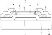
이하, 도 7을 참조하여 본 발명의 제2 실시 예에 대해 설명한다. 도 7은 본 발명의 제2 실시 예에 의한 산화물 반도체 물질을 포함하는 박막 트랜지스터 기판의 구조를 나타내는 단면도이다. 도 7을 참조하면, 본 발명의 제2 실시 예에 의한 박막 트랜지스터 기판은, 기판(SUB) 위에 매트릭스 방식으로 배치된 다수 개의 박막 트랜지스터(T)들을 포함한다. 여기서, 편의상 하나의 박막 트랜지스터(T)의 구조에 대해 설명한다.Hereinafter, a second embodiment of the present invention will be described with reference to FIG. 7 . 7 is a cross-sectional view illustrating a structure of a thin film transistor substrate including an oxide semiconductor material according to a second embodiment of the present invention. Referring to FIG. 7 , the thin film transistor substrate according to the second embodiment of the present invention includes a plurality of thin film transistors T disposed on the substrate SUB in a matrix manner. Here, for convenience, the structure of one thin film transistor T will be described.
제1 실시 예에서는, 단일 박막 트랜지스터에서, 고 이동도 특성 및 신뢰성 유지의 특징을 갖는 IGZTO의 함량에 대해 설명하였다. 본 발명은 대면적 표시 장치에 적용하기 위한 박막 트랜지스터 기판에 관한 것이다. 따라서, 제2 실시 예에서는, 대면적 및/또는 초고해상도를 구현하기 위한 평판 표시장치에서, 고 이동도 특성 및 신뢰성 향상의 특징을 갖는 IGZTO를 구비한 박막 트랜지스터 기판에 대해 설명한다. 특히, 제2 실시 예에서는, 대면적 표시장치용 박막 트랜지스터 기판을 제조하기 위한 공정 환경 및 제조 수율 등을 고려하여 가장 바람직한 구조를 갖는 박막 트랜지스터 기판에 대해 설명한다.In the first embodiment, in a single thin film transistor, the content of IGZTO having the characteristics of maintaining high mobility and reliability has been described. The present invention relates to a thin film transistor substrate for application to a large area display device. Accordingly, in the second embodiment, in a flat panel display for realizing a large area and/or ultra-high resolution, a thin film transistor substrate having an IGZTO having high mobility characteristics and improved reliability will be described. In particular, in the second embodiment, a thin film transistor substrate having the most desirable structure will be described in consideration of a process environment and manufacturing yield for manufacturing the thin film transistor substrate for a large area display device.
도 7을 참조하면, 기판(SUB) 상부 표면 전체에는 버퍼 층(BUF)이 적층되어 있다. 버퍼 층(BUF)은 기판(SUB) 위에 형성되는 여러 소자와의 계면 특성을 향상하기 위해 혹은 기판(SUB) 표면의 평탄성을 향상하기 위한 것이다.Referring to FIG. 7 , a buffer layer BUF is stacked on the entire upper surface of the substrate SUB. The buffer layer BUF is used to improve interface characteristics with various devices formed on the substrate SUB or to improve the flatness of the surface of the substrate SUB.
버퍼 층(BUF) 위에는 게이트 전극(G)이 배치되어 있다. 게이트 전극(G) 위에는 기판(SUB) 전체 표면을 덮는 게이트 절연막(GI)이 적층되어 있다. 게이트 절연막(GI)은 하층에 배치된 질화막(SIN)과 상층에 배치된 산화막(SIO)을 포함할 수 있다. 질화막(SIN)은 질화 실리콘(SiNx)을 포함할 수 있다. 산화막(SIO)은 산화 실리콘(SiOx)을 포함할 수 있다.A gate electrode G is disposed on the buffer layer BUF. A gate insulating layer GI is stacked on the gate electrode G to cover the entire surface of the substrate SUB. The gate insulating layer GI may include a nitride layer SIN disposed on a lower layer and an oxide layer SIO disposed on an upper layer. The nitride layer SIN may include silicon nitride (SiNx). The oxide layer SIO may include silicon oxide (SiOx).
특히, 게이트 전극(G)에 구리와 같은 저 저항 금속 물질을 사용하는 경우, 금속 확산 침투를 방지하는 데 유리한 질화 실리콘(SiNx)을 게이트 절연막으로 사용하는 것이 바람직하다. 질화막(SIN)의 경우, 제조 공정상 수소 입자를 다량 포함할 수 있다. 이러한 수소 입자들이 제조 공정 중에 그 위에 형성되는 산화물 반도체 층(A)으로 확산될 수 있다. 그 결과 산화물 반도체 층(A)의 NBTIS 특성이 열화될 수 있다. 본 발명의 제2 실시 예에서는, 질화막(SIN) 위에 산화막(SIO)을 적층 함으로써, 수소 입자가 산화물 반도체 층(A)으로 과다하게 확산되는 것을 방지할 수 있다.In particular, when a low-resistance metal material such as copper is used for the gate electrode G, it is preferable to use silicon nitride (SiNx), which is advantageous for preventing metal diffusion penetration, as the gate insulating layer. In the case of the nitride film (SIN), a large amount of hydrogen particles may be included in the manufacturing process. These hydrogen particles may diffuse into the oxide semiconductor layer (A) formed thereon during the manufacturing process. As a result, the NBTIS characteristics of the oxide semiconductor layer (A) may be deteriorated. In the second embodiment of the present invention, by stacking the oxide film SIO on the nitride film SIN, excessive diffusion of hydrogen particles into the oxide semiconductor layer A can be prevented.
게이트 절연막(GI) 위에는 게이트 전극(G)과 중첩하는 산화물 반도체 층(A)이 형성되어 있다. 산화물 반도체 층(A)은 1,000Å 이하의 두께를 갖는 금속 산화물로서, 인듐(Indium: In), 갈륨(Gallium: Ga), 아연(Zinc: Zn) 및 주석(Tin: Sn)의 산화물인 IGZTO를 포함한다. 바람직하게는, 산화물 반도체 층(A)은 300 Å 내지 700 Å 의 두께를 가질 수 있다. IGZTO 반도체 층(A)은 기본적으로 IGZO의 구성을 가지고 있으므로, 산화물 반도체 물질의 주요 특징인 우수한 오프-특성을 갖는다. 즉, 박막 트랜지스터가 오프(Off) 상태에서 누설되는 전류량이 적어, 화소의 전기적 특성을 오랫동안 일정하게 유지할 수 있다. 또한, IGZO에 주석(Tin: Sn)을 더 포함함으로써, IGZO보다 우수한 고 이동도 특성을 갖는다.An oxide semiconductor layer A overlapping the gate electrode G is formed on the gate insulating layer GI. Oxide semiconductor layer (A) is a metal oxide having a thickness of 1,000 Å or less, indium (Indium: In), gallium (Gallium: Ga), zinc (Zinc: Zn) and IGZTO, which is an oxide of tin (Tin: Sn) include Preferably, the oxide semiconductor layer (A) may have a thickness of 300 Å to 700 Å. Since the IGZTO semiconductor layer (A) has the composition of IGZO basically, it has excellent off-characteristics, which are the main characteristics of oxide semiconductor materials. That is, since the amount of current leaking from the thin film transistor in the OFF state is small, the electrical characteristics of the pixel can be maintained constant for a long time. In addition, by further including tin (Tin: Sn) in IGZO, it has excellent high mobility properties than IGZO.
고 이동도 특성은 박막 트랜지스터의 On-Off 절환을 신속하게 수행할 수 있다는 장점이 있다. 고속 구동을 반복하다 보면, 반도체 소자가 열화되어 고속 특성이 급격히 저하될 수 있다. 따라서, 고 이동도 특성을 구현하는 경우, 신뢰성을 확보하는 것이 중요하다. IGZO에 고 이동도 특성을 부여할 수 있는 여러 물질 중에서도, 본 발명에서 제안한 바와 같이, 주석을 사용할 때 신뢰성 열화가 거의 발생하지 않는다. 특히, 산화물 반도체 층(A)은 제1 실시 예에서 설명한 바와 동일한 함량비를 갖는 것이 바람직하다.The high mobility characteristic has an advantage in that the on-off switching of the thin film transistor can be performed quickly. If the high-speed driving is repeated, the semiconductor device may be deteriorated and the high-speed characteristics may be rapidly deteriorated. Therefore, when implementing high mobility characteristics, it is important to secure reliability. Among the various materials that can impart high mobility properties to IGZO, as suggested in the present invention, reliability degradation hardly occurs when tin is used. In particular, the oxide semiconductor layer (A) preferably has the same content ratio as described in the first embodiment.
또한, IGZTO 반도체 물질에서 더 안정된 고 이동도 특성을 확보하기 위해서는 반도체 층(A)의 상층 표면을 N2O 플라즈마로 처리하는 것이 바람직하다. 그 결과, 반도체 층(A)의 상층 표면에는 산소 풍부 영역(OR)이 형성된다. 산소 풍부 영역(OR)은 IGZTO보다 산소 함량이 10~20% 정도 더 많이 포함된 특성을 갖는다. 산소 풍부 영역(OR)의 두께는 최대 10nm 정도로 아주 얇게 형성된다. 산소 풍부 영역(OR)은 산화물 반도체 층(A) 위에 추가로 적층하여 형성한 것이 아니다. 산화물 반도체 층(A)의 표면에 N2O 플라즈마로 표면 처리를 수행하여, 산화물 반도체 층(A)의 상층부 일부 두께에 산소를 더 많이 포함하는 부분이다.In addition, in order to secure more stable high mobility characteristics in the IGZTO semiconductor material, it is preferable to treat the upper surface of the semiconductor layer (A) with N2 O plasma. As a result, an oxygen-rich region OR is formed on the upper surface of the semiconductor layer A. The oxygen-rich region (OR) has a characteristic in which the oxygen content is 10-20% higher than that of IGZTO. The thickness of the oxygen-rich region (OR) is formed to be very thin, up to about 10 nm. The oxygen-rich region OR is not formed by additionally stacking on the oxide semiconductor layer (A). The surface of the oxide semiconductor layer (A) is subjected to surface treatment with N2 O plasma, and the upper layer portion of the oxide semiconductor layer (A) contains more oxygen in a partial thickness.
산화물 반도체 층(A) 위에는 소스 전극(S)과 드레인 전극(D)이 접촉하고 있다. 소스 전극(S)과 드레인 전극(D)은 일정 거리 이격하여 분리되어 있다. 즉, 소스 전극(S)은 산화물 반도체 층(A)의 일측 상변과 접촉하고, 드레인 전극(D)은 반도체 층(A)의 타측 상변과 접촉한다. 또한, IGZTO 반도체 물질을 포함하는 박막 트랜지스터(T)를 덮는 보호막(PAS)이 기판(SUB) 전체를 덮도록 형성되어 있다.On the oxide semiconductor layer (A), the source electrode (S) and the drain electrode (D) are in contact. The source electrode S and the drain electrode D are separated from each other by a predetermined distance. That is, the source electrode S is in contact with the upper side of one side of the oxide semiconductor layer (A), and the drain electrode (D) is in contact with the upper side of the other side of the semiconductor layer (A). In addition, a passivation layer PAS covering the thin film transistor T including the IGZTO semiconductor material is formed to cover the entire substrate SUB.
IGZTO 반도체 물질을 포함하는 박막 트랜지스터 기판을 평판형 표시 장치에 적용하는 경우, 도면으로 도시하지 않았으나, 보호막(PAS)에는 드레인 전극(D)을 노출하는 콘택홀을 더 형성할 수 있다. 또한, 보호막(PAS) 위에는 콘택홀을 통해 드레인 전극(D)과 연결된 화소 전극이 형성되어 있을 수 있다.When a thin film transistor substrate including an IGZTO semiconductor material is applied to a flat panel display device, a contact hole exposing the drain electrode D may be further formed in the passivation layer PAS, although not shown in the drawings. Also, a pixel electrode connected to the drain electrode D through a contact hole may be formed on the passivation layer PAS.
이하, 도 7 및 8을 참조하여, 본 발명의 제2 실시 예에 의한 산화물 반도체 물질을 포함하는 박막 트랜지스터 기판을 제조하는 고정을 설명한다. 도 8은 본 발명의 제2 실시 예에 의한 산화물 반도체 물질을 포함하는 박막 트랜지스터 기판을 제조하는 공정을 나타내는 순서도이다.Hereinafter, fixing for manufacturing a thin film transistor substrate including an oxide semiconductor material according to a second embodiment of the present invention will be described with reference to FIGS. 7 and 8 . 8 is a flowchart illustrating a process of manufacturing a thin film transistor substrate including an oxide semiconductor material according to a second embodiment of the present invention.
기판(SUB) 위에 구리와 같은 저 저항 금속 물질을 증착한다. 제1 마스크 공정으로 금속 물질 층을 패턴하여, 게이트 전극(G)을 형성한다. 게이트 전극(G)을 연결하는 게이트 배선을 함께 형성할 수 있다. 게이트 전극(G)을 형성하기 전에, 특히, 저 저항 금속 물질을 증착하기 전에, 버퍼 층(BUF)을 먼저 증착할 수 있다. (S100)A low-resistance metal material such as copper is deposited on the substrate SUB. A gate electrode G is formed by patterning the metal material layer in a first mask process. A gate line connecting the gate electrode G may be formed together. Before forming the gate electrode G, in particular, before depositing a low-resistance metal material, the buffer layer BUF may be first deposited. (S100)
게이트 전극(G)이 형성된 기판(SUB) 상부 표면 위에 게이트 절연막(GI)을 증착한다. 특히, 질화막(SIN)을 먼저 증착하고, 그 위에 산화막(SIO)을 증착하는 것이 바람직하다. (S110)A gate insulating layer GI is deposited on the upper surface of the substrate SUB on which the gate electrode G is formed. In particular, it is preferable to first deposit the nitride film SIN, and then deposit the oxide film SIO thereon. (S110)
게이트 절연막(GI) 위에 인듐(Indium: In), 갈륨(Gallium: Ga), 아연(Zinc: Zn) 및 주석(Tin: Sn)의 합금을 산소 분위기 상태에서 증착하여, IGZTO 층을 형성한다. 특히, 기판(SUB)의 온도를 150℃ 내지 250℃의 상태로 (가장 바람직하게는 200℃) 가열한 고온에서 증착 공정을 수행하는 것이 바람직하다. 제2 마스크 공정으로 IGZTO 층을 패턴하여 산화물 반도체 층(A)을 형성한다. (S200)An IGZTO layer is formed by depositing an alloy of indium (In), gallium (Ga), zinc (Zinc: Zn), and tin (Tin: Sn) on the gate insulating layer GI in an oxygen atmosphere. In particular, it is preferable to perform the deposition process at a high temperature in which the temperature of the substrate SUB is heated to a state of 150° C. to 250° C. (most preferably 200° C.). An oxide semiconductor layer (A) is formed by patterning the IGZTO layer by a second mask process. (S200)
산화물 반도체 층(A)이 형성된 기판(SUB)의 상부 표면 위에 몰리브덴(Mo), 티타늄(Ti), 구리(Cu) 및 이들의 합금을 증착하여 소스-드레인 금속 층을 형성한다. 특히, 몰리브덴-티타늄(MoTi), 구리(Cu) 및 몰리브덴-티타늄(MoTi)이 순차적으로 적층된 3중층 금속층을 형성하는 것이 바람직하다. 제3 마스크 공정으로 소스-드레인 금속층을 패턴하여, 소스 전극(S) 및 드레인 전극(D)을 형성한다. 도면에 도시하지 않았지만, 소스 전극(S)을 연결하는 데이터 배선을 더 형성할 수 있다. (S300)A source-drain metal layer is formed by depositing molybdenum (Mo), titanium (Ti), copper (Cu), and alloys thereof on the upper surface of the substrate SUB on which the oxide semiconductor layer A is formed. In particular, it is preferable to form a triple-layered metal layer in which molybdenum-titanium (MoTi), copper (Cu), and molybdenum-titanium (MoTi) are sequentially stacked. A source electrode S and a drain electrode D are formed by patterning the source-drain metal layer by a third mask process. Although not shown in the drawing, a data line connecting the source electrode S may be further formed. (S300)
소스-드레인 전극(S-D)이 형성된 기판(SUB)의 상부 표면 위에 N2O 플라즈마로 표면을 처리한다. 플라즈마 처리를 장시간 수행하거나 에너지가 과도할 경우, PBTS의 특성이 열화되는 역효과가 발생할 수 있다. 따라서, 플라즈마 처리는 2~3kW/㎡ 범위의 에너지로 수행하는 것이 바람직하다. 그 결과, 소스 전극(S)과 드레인 전극(D) 사이에 노출된 산화물 반도체 층(A)에는, 두께가 10nm 이하인, 산소 풍부 영역(OR)이 형성된다. (S310)The surface is treated with N2O plasma on the upper surface of the substrate SUB on which the source-drain electrodes S-D are formed. If the plasma treatment is performed for a long time or if the energy is excessive, the adverse effect of deterioration of the characteristics of the PBTS may occur. Therefore, the plasma treatment is preferably performed with an energy in the range of 2 to 3 kW/
산소 풍부 영역(OR)이 형성된 기판(SUB)의 상부 표면 위에 무기 절연 물질을 증착하여 보호막(PAS)을 형성한다. 특히, 산화물 반도체 층(A)에 수소와 같은 물질이 확산되지 않도록 산화 실리콘(SiOx)을 포함하는 산화막(SIO)을 증착하는 것이 바람직하다. (S320)A passivation layer PAS is formed by depositing an inorganic insulating material on the upper surface of the substrate SUB on which the oxygen rich region OR is formed. In particular, it is preferable to deposit an oxide film (SIO) including silicon oxide (SiOx) so that a material such as hydrogen does not diffuse into the oxide semiconductor layer (A). (S320)
본 발명에 의한 박막 트랜지스터를 평판 표시장치에 적용하는 경우, 제4 마스크 공정으로 보호막(PAS)을 패턴하여 드레인 전극(D)의 일부를 노출하는 콘택홀을 형성한다. (S400)When the thin film transistor according to the present invention is applied to a flat panel display, a contact hole exposing a part of the drain electrode D is formed by patterning the passivation layer PAS by a fourth mask process. (S400)
보호막(PAS) 위에 인듐-아연 산화물(Indium-Zinc Oxide; IZO) 혹은 인듐-주석 산화물(Indium-Tin Oxide; ITO)과 같은 투명 도전 물질을 증착한다. 제5 마스크 공정으로 투명 도전 물질을 패턴하여, 화소 전극을 형성한다. 화소 전극은 콘택홀을 통해 드레인 전극(D)과 전기적/물리적으로 연결된다. (S500)A transparent conductive material such as indium-zinc oxide (IZO) or indium-tin oxide (ITO) is deposited on the passivation layer PAS. A pixel electrode is formed by patterning a transparent conductive material in a fifth mask process. The pixel electrode is electrically/physically connected to the drain electrode D through a contact hole. (S500)
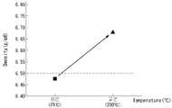
이상 설명한 본 발명의 제2 실시 예에 의한 박막 트랜지스터 기판의 제조 공정에는 두 가지 중요한 특징이 있다. 첫 번째 특징은, IGZTO를 포함하는 산화물 반도체 물질 층을 기판(SUB)의 온도가 150℃ 내지 250℃ 사이의 고온인 상태에서 (가장 바람직하게는 200℃) 증착하는 것이다. 그 결과, IGZTO 산화물 반도체 층(A)은 C축 결정 구조를 갖는다. 이와 같은 결정성으로 인해, IGZTO 산화물 반도체 층(A)은 결함이 감소되고 밀도가 증가하여 우수한 소자 특성을 가질 수 있다.The manufacturing process of the thin film transistor substrate according to the second embodiment of the present invention described above has two important characteristics. The first feature is that the oxide semiconductor material layer including IGZTO is deposited at a high temperature of the substrate SUB between 150° C. and 250° C. (most preferably 200° C.). As a result, the IGZTO oxide semiconductor layer (A) has a C-axis crystal structure. Due to such crystallinity, the IGZTO oxide semiconductor layer (A) may have excellent device properties by reducing defects and increasing the density.
IGZO의 경우, 산화물 반도체 층(A)은 이론적으로 최대 밀도는 6.50g/㎤ 미만인 값을 갖는다. 반면에 IGZTO의 경우, 이론적인 밀도 값은 7.00g/㎤이다. 본 발명에서는 기판(SUB)을 150℃ 내지 250℃ 사이의 고온 상태에서 산화물 반도체 층(A)을 증착함으로써, 밀도가 6.50g/㎤ 이상인 IGZTO 산화물 반도체 층(A)을 얻을 수 있었다. 도 9는 본 발명의 제2 실시 예에 의한 산화물 반도체 물질 층의 밀도 특성이 향상된 결과를 나타내는 그래프이다.In the case of IGZO, the oxide semiconductor layer (A) has a theoretical maximum density of less than 6.50 g/cm 3 . On the other hand, for IGZTO, the theoretical density value is 7.00 g/cm 3 . In the present invention, the IGZTO oxide semiconductor layer (A) having a density of 6.50 g/cm 3 or more was obtained by depositing the oxide semiconductor layer (A) on the substrate (SUB) at a high temperature between 150°C and 250°C. 9 is a graph showing the result of improved density characteristics of the oxide semiconductor material layer according to the second embodiment of the present invention.
도 9를 참조하면, 상온(Room Temperature; 25℃)에서 IGZTO 반도체 층을 형성하는 경우, 아몰퍼스(amorphous) 상태로 형성되고, 밀도 값은 6.50g/㎤을 넘지 못한다. 하지만, 기판(SUB) 온도를 200℃ 정도로 가열한 상태에서 IGZTO 반도체 층을 형성하는 경우, C축 결정성을 가지며, 밀도 값은 6.60g/㎤ 내지 6.70g/㎤의 값을 가질 수 있음을 알 수 있다.Referring to FIG. 9 , when the IGZTO semiconductor layer is formed at room temperature (25° C.), it is formed in an amorphous state, and the density value does not exceed 6.50 g/cm 3 . However, when the IGZTO semiconductor layer is formed while the substrate (SUB) temperature is heated to about 200°C, it has C-axis crystallinity and the density value can have a value of 6.60 g/cm 3 to 6.70 g/cm 3 can
여기서, 산화물 반도체 층(A)의 밀도는 XRR(X-ray reflectivity, X-ray specular reflectivity or X-ray reflectometry) 방식으로 측정한 값이다. XRR은 표면 감지 분석 기술로서, 표면, 박막 및 다층체의 특성을 평가하는 방식 및 장비이다.Here, the density of the oxide semiconductor layer (A) is a value measured by an X-ray reflectivity, X-ray specular reflectivity, or X-ray reflectometry (XRR) method. XRR is a surface sensing analysis technology, a method and equipment for evaluating the properties of surfaces, thin films and multilayers.
본 발명의 제2 실시 예에서, 산화물 반도체 층(A)의 밀도를 6.50g/㎤ 이상을 갖도록 하는 이유는 쇼트 채널을 구현하기 위한 것이다. 이하, 도 10a 및 10b를 참조하여, 이에 대해 상세히 설명한다. 도 10a 및 10b는 본 발명의 제2 실시 예에 의한 산화물 반도체 물질층이 갖는 고 밀도 특성을 설명하는 단면도이다.In the second embodiment of the present invention, the reason for making the density of the oxide semiconductor layer (A) to be 6.50 g/cm 3 or more is to implement a short channel. Hereinafter, with reference to FIGS. 10A and 10B, this will be described in detail. 10A and 10B are cross-sectional views illustrating high-density characteristics of an oxide semiconductor material layer according to a second embodiment of the present invention.
도 10a는 상온 상태에서 IGZTO 반도체 층(A)을 형성한 경우를 나타낸다. 도 10a를 참조하면, 반도체 층(A)에서 소스 전극(S)과 드레인 전극(D) 사이의 길이가 채널 길이(CH length)로 정의된다. 반도체 층(A)에서 소스 전극(S)과 접촉하는 영역을 소스 영역(SA)으로, 드레인 전극(D)과 접촉하는 영역을 드레인 영역(DA)으로 정의한다.10A shows a case in which the IGZTO semiconductor layer (A) is formed at room temperature. Referring to FIG. 10A , a length between the source electrode S and the drain electrode D in the semiconductor layer A is defined as a channel length CH length. In the semiconductor layer A, a region in contact with the source electrode S is defined as a source region SA, and a region in contact with the drain electrode D is defined as a drain region DA.
이러한 구조에서, 박막 트랜지스터(T)가 작동되면, 소스 전극(S) 및 드레인 전극(D)에 유도된 전하에 의해 소스 영역(SA)과 드레인 영역(DA) 형성된다. 이 때, 반도체 층(A)의 밀도가 6.50g/㎤ 미만으로 낮은 경우 소스 영역(SA)과 드레인 영역(DA)이 확산된다. 그 결과, 실질적인 유효한 채널 길이(CHeff. length)가 축소된다. 예를 들어, 4㎛의 유효 채널 길이(CHeff. length)를 구현하기 위해서는, 소스 영역(SA)과 드레인 영역(DA)의 확산 정도를 고려하여, 채널 길이(CH length)는 4㎛보다 훨씬 길게 형성하여야 한다. 즉, 쇼트 채널 설계가 매우 어렵고, 이로 인해, 초 고해상도 평판 표시장치용 박막 트랜지스터 기판을 구현하는 것이 매우 어려울 수 있다.In this structure, when the thin film transistor T is operated, a source region SA and a drain region DA are formed by charges induced in the source electrode S and the drain electrode D. In this case, when the density of the semiconductor layer A is low, less than 6.50 g/cm 3 , the source region SA and the drain region DA are diffused. As a result, the effective effective channel length CHeff. length is reduced. For example, in order to implement an effective channel length CHeff. length of 4 μm, the channel length CH length is much longer than 4 μm in consideration of the diffusion degree of the source area SA and the drain area DA. should be formed That is, it is very difficult to design a short channel, and thus, it may be very difficult to implement a thin film transistor substrate for an ultra-high resolution flat panel display.
하지만, IGZTO 반도체 층(A)의 밀도를 6.50g/㎤ 이상으로 형성하는 경우, 도 10b에서와같이, 쇼트 채널을 형성할 수 있다. 도 10b는 고온 상태에서 IGZTO 반도체 층(A)을 형성한 경우를 나타낸다. 도 10b를 참조하면, 박막 트랜지스터(T)의 작동 상태에서 소스 영역(SA) 및 드레인 영역(DA)은 실제 소스 전극(S) 및 드레인 전극(D)의 경계부에서 확산되는 정도가 매우 적다. 따라서, 실질적인 유효 채널 길이(CHeff. length)는 채널 길이(CH length)와 거의 동일하다. 따라서, 채널 길이(CH length)를 4㎛ 정도로 형성하여, 4㎛의 유효 채널 길이(CHeff. length)를 얻을 수 있다. 즉, 쇼트 채널 설계가 용이하며, 초 고해상도 평판 표시장치용 박막 트랜지스터 기판을 구현하기 용이하다.However, when the density of the IGZTO semiconductor layer (A) is formed to be 6.50 g/cm 3 or more, as in FIG. 10b , a short channel may be formed. 10B shows a case in which the IGZTO semiconductor layer (A) is formed in a high temperature state. Referring to FIG. 10B , in the operating state of the thin film transistor T, the diffusion degree of the source area SA and the drain area DA at the boundary between the source electrode S and the drain electrode D is very small. Accordingly, the effective effective channel length CHeff. length is approximately equal to the channel length CH length. Accordingly, by forming a channel length (CH length) of about 4 µm, an effective channel length (CHeff. length) of 4 µm can be obtained. That is, it is easy to design a short channel and to implement a thin film transistor substrate for an ultra-high resolution flat panel display.
본 발명의 제2 실시 예에서 두 번째 특징은, 산화물 반도체 층(A)에서 소스 전극(S)과 드레인 전극(D) 사이에 산소 풍부 영역(OR)을 구비한 구조에 있다. 특히, 산소 풍부 영역(OR)은 산화물 반도체 층(A) 전체 두께의 30%를 초과하지 않는 것이 바람직하다. 특히, 산소 풍부 영역(OR)은 산화물 반도체 층(A) 두께의 20%인 것이 가장 바람직하다. 예를 들어, 산화물 반도체 층(A)의 두께가 500Å(50nm)인 경우, 산소 풍부 영역(OR)은 100Å(10nm)인 것이 바람직하며, 최대 150Å(15nm)을 넘지 않는 것이 좋다.A second feature in the second embodiment of the present invention lies in a structure in which an oxygen-rich region OR is provided between the source electrode S and the drain electrode D in the oxide semiconductor layer A. In particular, the oxygen-rich region OR preferably does not exceed 30% of the total thickness of the oxide semiconductor layer (A). In particular, the oxygen-rich region OR is most preferably 20% of the thickness of the oxide semiconductor layer A. For example, when the thickness of the oxide semiconductor layer A is 500 Å (50 nm), the oxygen-rich region OR is preferably 100 Å (10 nm), and preferably does not exceed 150 Å (15 nm) at most.
이하, 도 11을 참조하여, 산소 풍부 영역(OR)의 두께 한정에 대해 설명한다. 도 11은 본 발명의 제2 실시 예에 의한 산소 풍부 영역을 구비한 산화물 반도체 물질 층의 구조를 나타내는 단면도이다.Hereinafter, the thickness limitation of the oxygen-rich region OR will be described with reference to FIG. 11 . 11 is a cross-sectional view illustrating a structure of an oxide semiconductor material layer having an oxygen-rich region according to a second embodiment of the present invention.
박막 트랜지스터(T)가 작동하면, 즉, 게이트 전극(G)에 전압이 인가되어 전기장이 반도체 층(A)에 인가된다. 이 때, 50nm 두께의 반도체 층(A)에서, 반도체 층(A)에서 게이트 전극(G)에 가까운 하부 층의 일부 두께(예를 들어, 2~3nm)에는 채널 영역(CH)이 형성된다. 그리고 반도체 층(A)의 상부 층에는 10~15nm 두께의 산소 풍부 영역(OR)이 형성되어 있다. 그 결과, 산소 풍부 영역(OR)과 채널 영역(CH) 사이에는 38~32nm 두께의 버퍼 영역(BA)이 형성된다.When the thin film transistor T is activated, that is, a voltage is applied to the gate electrode G so that an electric field is applied to the semiconductor layer A. In this case, in the semiconductor layer (A) having a thickness of 50 nm, a channel region (CH) is formed in a partial thickness (eg, 2-3 nm) of the lower layer close to the gate electrode (G) in the semiconductor layer (A). In addition, an oxygen-rich region OR having a thickness of 10 to 15 nm is formed on the upper layer of the semiconductor layer (A). As a result, a buffer region BA having a thickness of 38 to 32 nm is formed between the oxygen-rich region OR and the channel region CH.
산소 풍부 영역(OR)은 다른 부분보다 산소의 함량이 10~20% 정도 더 많이 포함되어 있다. 산소 함량이 20%를 넘을 경우, 산소 풍부 영역(OR)이 도체 영역으로 작동하여, 스위칭 기능을 할 수 없다. 또한, 산소 풍부 영역(OR)이 너무 두꺼워 질 경우, 버퍼 영역(BA)을 줄이고, 채널 영역(CH)으로 산소 풍부 영역(OR)이 영향을 주어, 반도체 층(A)의 특성이 원하지 않은 상태로 변질될 수 있다. 따라서, 산소 풍부 영역(OR)은 그 두께 및 산소 함량을 최적의 상태로 유지하는 것이 매우 중요하다.The oxygen-rich region (OR) contains 10 to 20% more oxygen than other parts. When the oxygen content exceeds 20%, the oxygen rich region (OR) acts as a conductor region, and the switching function cannot be performed. In addition, when the oxygen-rich region OR becomes too thick, the buffer region BA is reduced, and the oxygen-rich region OR affects the channel region CH, so that the characteristics of the semiconductor layer A are undesirable. can be transformed into Therefore, it is very important to keep the thickness and oxygen content of the oxygen rich region OR in an optimal state.
이상 설명한 내용을 통해 당업자라면 본 발명의 기술 사상을 일탈하지 아니하는 범위 내에서 다양한 변경 및 수정이 가능함을 알 수 있을 것이다. 따라서, 본 발명은 상세한 설명에 기재된 내용으로 한정되는 것이 아니라 특허 청구 범위에 의해 정해져야만 할 것이다.Those skilled in the art from the above description will be able to see that various changes and modifications can be made without departing from the technical spirit of the present invention. Accordingly, the present invention should not be limited to the contents described in the detailed description, but should be defined by the claims.
T: 박막 트랜지스터SUB: 기판
GL: 게이트 배선CL: 공통 배선
DL: 데이터 배선PXL: 화소 전극
G: 게이트 전극SE, A: 반도체 층
S: 소스 전극D: 드레인 전극
GI: 게이트 절연막PAS: 보호막
PAC: 평탄화 막DH: 드레인 콘택홀
SL: 스캔 배선ST: 스위칭 박막 트랜지스터
DT: 구동 박막 트랜지스터OLE: 유기발광 다이오드
SE, DE: 에치 스토퍼PH: 화소 콘택홀
CAT: 캐소드 전극(층)ANO: 애노드 전극(층)
OR: 산소 풍부 산화물 반도체 층T: thin film transistor SUB: substrate
GL: Gate wiring CL: Common wiring
DL: data wiring PXL: pixel electrode
G: gate electrode SE, A: semiconductor layer
S: source electrode D: drain electrode
GI: gate insulating film PAS: protective film
PAC: planarization film DH: drain contact hole
SL: scan wiring ST: switching thin film transistor
DT: driving thin film transistor OLE: organic light emitting diode
SE, DE: etch stopper PH: pixel contact hole
CAT: cathode electrode (layer) ANO: anode electrode (layer)
OR: oxygen-rich oxide semiconductor layer
Claims (18)
Translated fromKorean상기 기판 위에 배치된 게이트 전극;
상기 게이트 전극을 덮는 게이트 절연막;
상기 게이트 절연막 위에서 상기 게이트 전극과 중첩하여 배치된 산화물 반도체 층;
상기 산화물 반도체 층의 일측 상부 표면, 상기 산화물 반도체 층의 일측 측면 및 상기 게이트 절연막과 접촉하는 소스 전극; 그리고
상기 산화물 반도체 층의 타측 상부 표면, 상기 산화물 반도체 층의 타측 측면 및 상기 게이트 절연막과 접촉하는 드레인 전극을 구비하되,
상기 산화물 반도체 층은,
인듐, 갈륨, 아연 및 주석을 포함하되,
상기 인듐에 대한 상기 주석의 함량비는 10% 내지 25% 사이의 어느 한 값을 가지며,
상기 산화물 반도체 층은, 채널 영역, 버퍼 영역 및 산소 풍부 영역을 포함하고,
상기 버퍼 영역은 상기 산소 풍부 영역과 상기 채널 영역 사이에 형성되고,
상기 산소 풍부 영역은 상기 소스 전극과 상기 드레인 전극 사이에서, 일정 두께를 차지하며,
상기 산소 풍부 영역은, 상기 산화물 반도체 층의 다른 영역보다 10% 내지 20% 산소 함량이 더 많으며,
상기 산소 풍부 영역은, 상기 산화물 반도체 층 전체 두께의 20% 내지 30%의 두께를 가지며,
상기 산소 풍부 영역은 상기 소스 전극 및 상기 드레인 전극과 중첩하지 않는, 박막 트랜지스터 기판.
Board;
a gate electrode disposed on the substrate;
a gate insulating film covering the gate electrode;
an oxide semiconductor layer disposed on the gate insulating layer to overlap the gate electrode;
a source electrode in contact with one upper surface of the oxide semiconductor layer, one side of the oxide semiconductor layer, and the gate insulating layer; and
a drain electrode in contact with the other upper surface of the oxide semiconductor layer, the other side of the oxide semiconductor layer, and the gate insulating layer;
The oxide semiconductor layer,
including indium, gallium, zinc and tin;
The content ratio of the tin to the indium has any value between 10% and 25%,
The oxide semiconductor layer includes a channel region, a buffer region, and an oxygen-rich region,
the buffer region is formed between the oxygen-rich region and the channel region;
The oxygen-rich region occupies a predetermined thickness between the source electrode and the drain electrode,
The oxygen-rich region has a 10% to 20% oxygen content higher than other regions of the oxide semiconductor layer,
The oxygen-rich region has a thickness of 20% to 30% of the total thickness of the oxide semiconductor layer,
The oxygen-rich region does not overlap the source electrode and the drain electrode.
상기 인듐과 상기 아연의 함량비는 동일한 값을 갖는 박막 트랜지스터 기판.
The method of claim 1,
A thin film transistor substrate having the same content ratio of the indium and the zinc.
상기 갈륨의 함량비는 상기 인듐의 함량비보다 작은 값을 갖는 박막 트랜지스터 기판.
The method of claim 1,
The thin film transistor substrate having a content ratio of the gallium smaller than the content ratio of indium.
상기 산화물 반도체 층은,
6.50g/㎤ 내지 7.00g/㎤의 밀도 값을 갖는 박막 트랜지스터 기판.
The method of claim 1,
The oxide semiconductor layer,
A thin film transistor substrate having a density value of 6.50 g/cm 3 to 7.00 g/cm 3 .
상기 게이트 전극을 덮는 게이트 절연막을 증착하는 단계;
상기 게이트 절연막 위에 상기 게이트 전극과 중첩하며, 인듐, 갈륨, 아연 및 주석을 포함하는 산화물 반도체 층을 형성하는 단계;
상기 산화물 반도체 층의 일측부와 접촉하는 소스 전극 및 타측부와 접촉하는 드레인 전극을 형성하는 단계;
상기 소스 전극 및 상기 드레인 전극 사이에 노출된 상기 산화물 반도체 층의 표면에 산소 풍부 영역을 형성하는 단계; 그리고
상기 소스 전극, 상기 드레인 전극 및 상기 산화물 반도체 층을 덮는 보호막을 형성하는 단계를 포함하며,
상기 산화물 반도체 층은, 채널 영역, 버퍼 영역 및 산소 풍부 영역을 포함하고,
상기 버퍼 영역은 상기 산소 풍부 영역과 상기 채널 영역 사이에 형성되고,
상기 산소 풍부 영역은, 상기 산화물 반도체 층의 다른 영역보다 10% 내지 20% 산소 함량이 더 많으며,
상기 산소 풍부 영역은, 상기 산화물 반도체 층 전체 두께의 20% 내지 30%의 두께를 가지며,
상기 산소 풍부 영역을 형성하는 단계는 상기 소스 전극 및 상기 드레인 전극을 형성하는 단계 이후에 이루어지며,
상기 산소 풍부 영역은 상기 소스 전극 및 상기 드레인 전극과 중첩하지 않고,
상기 소스 전극은 상기 산화물 반도체 층의 일측 상부 표면, 상기 산화물 반도체 층의 일측 측면 및 상기 게이트 절연막과 접촉하고,
상기 드레인 전극은 상기 산화물 반도체 층의 타측 상부 표면, 상기 산화물 반도체 층의 타측 측면 및 상기 게이트 절연막과 접촉하는, 박막 트랜지스터 기판 제조 방법.
forming a gate electrode on the substrate;
depositing a gate insulating layer covering the gate electrode;
forming an oxide semiconductor layer overlapping the gate electrode on the gate insulating layer and including indium, gallium, zinc and tin;
forming a source electrode in contact with one side of the oxide semiconductor layer and a drain electrode in contact with the other side of the oxide semiconductor layer;
forming an oxygen-rich region on a surface of the oxide semiconductor layer exposed between the source electrode and the drain electrode; and
forming a protective film covering the source electrode, the drain electrode, and the oxide semiconductor layer;
The oxide semiconductor layer includes a channel region, a buffer region, and an oxygen-rich region,
the buffer region is formed between the oxygen-rich region and the channel region;
The oxygen-rich region has a 10% to 20% oxygen content higher than other regions of the oxide semiconductor layer,
The oxygen-rich region has a thickness of 20% to 30% of the total thickness of the oxide semiconductor layer,
The forming of the oxygen-rich region is performed after forming the source electrode and the drain electrode,
the oxygen-rich region does not overlap the source electrode and the drain electrode;
the source electrode is in contact with one upper surface of the oxide semiconductor layer, one side of the oxide semiconductor layer, and the gate insulating layer;
The drain electrode is in contact with the upper surface of the other side of the oxide semiconductor layer, the other side of the oxide semiconductor layer, and the gate insulating film.
상기 산화물 반도체 층은,
상기 인듐에 대한 상기 주석의 함량비는 10% 내지 25% 사이의 어느 한 값을 갖는 박막 트랜지스터 기판 제조 방법.
9. The method of claim 8,
The oxide semiconductor layer,
The method of manufacturing a thin film transistor substrate having a content ratio of the tin to the indium having any value between 10% and 25%.
상기 산화물 반도체 층을 형성하는 단계는,
상기 기판을 150℃ 내지 250℃의 고온 상태에서 수행하는 박막 트랜지스터 기판 제조 방법.
9. The method of claim 8,
The step of forming the oxide semiconductor layer,
A method of manufacturing a thin film transistor substrate for performing the substrate at a high temperature of 150° C. to 250° C.
상기 산화물 반도체 층은, 6.50g/㎤ 내지 7.00g/㎤의 밀도 값을 갖는 박막 트랜지스터 기판 제조 방법.
11. The method of claim 10,
The oxide semiconductor layer is a thin film transistor substrate manufacturing method having a density value of 6.50 g/cm 3 to 7.00 g/cm 3 .
상기 산소 풍부 영역을 형성하는 단계는,
2~3kW/㎡ 범위의 에너지로 N2O 플라즈마 처리를 수행하는 박막 트랜지스터 기판 제조 방법.
9. The method of claim 8,
Forming the oxygen-rich region comprises:
A method of manufacturing a thin film transistor substrate for performing N2 O plasma treatment with an energy in the range of 2 to 3 kW/m2.
상기 게이트 절연막을 증착하는 단계는,
상기 게이트 전극 위에 질화막을 증착하는 단계; 그리고
상기 질화막 위에 산화막을 증착하는 단계를 포함하는 박막 트랜지스터 기판 제조 방법.9. The method of claim 8,
Depositing the gate insulating film comprises:
depositing a nitride film on the gate electrode; and
and depositing an oxide film on the nitride film.
상기 버퍼 영역은 상기 산화물 반도체 층 두께의 64 내지 76%의 두께를 갖는 박막 트랜지스터 기판.
The method of claim 1,
wherein the buffer region has a thickness of 64 to 76% of a thickness of the oxide semiconductor layer.
Priority Applications (9)
| Application Number | Priority Date | Filing Date | Title |
|---|---|---|---|
| KR1020170081022AKR102448483B1 (en) | 2017-06-27 | 2017-06-27 | Thin film transistor substrate having high mobility semiconductor material and method for manufacturing the same |
| CN201810567992.4ACN109148592B (en) | 2017-06-27 | 2018-06-05 | Thin film transistor including oxide semiconductor layer, method for manufacturing the same, and display device including the same |
| TW107119521ATWI673881B (en) | 2017-06-27 | 2018-06-06 | Thin-film transistor including oxide semiconductor layer, method of manufacturing the same, and display apparatus including the same |
| JP2018114108AJP6599518B2 (en) | 2017-06-27 | 2018-06-15 | Thin film transistor including oxide semiconductor layer, method for manufacturing the same, and display device |
| EP18179057.7AEP3422419B1 (en) | 2017-06-27 | 2018-06-21 | Thin-film transistor including oxide semiconductor layer, method of manufacturing the same, and display apparatus including the same |
| US16/019,294US10608117B2 (en) | 2017-06-27 | 2018-06-26 | Thin-film transistor including oxide semiconductor layer, method of manufacturing the same, and display apparatus including the same |
| US16/790,591US11201248B2 (en) | 2017-06-27 | 2020-02-13 | Thin-film transistor including oxide semiconductor layer, method of manufacturing the same, and display apparatus including the same |
| US17/524,255US12176437B2 (en) | 2017-06-27 | 2021-11-11 | Thin-film transistor including oxide semiconductor layer, method of manufacturing the same, and display apparatus including the same |
| US18/955,048US20250089301A1 (en) | 2017-06-27 | 2024-11-21 | Thin-film transistor including oxide semiconductor layer, method of manufacturing the same, and display apparatus including the same |
Applications Claiming Priority (1)
| Application Number | Priority Date | Filing Date | Title |
|---|---|---|---|
| KR1020170081022AKR102448483B1 (en) | 2017-06-27 | 2017-06-27 | Thin film transistor substrate having high mobility semiconductor material and method for manufacturing the same |
Publications (2)
| Publication Number | Publication Date |
|---|---|
| KR20190001279A KR20190001279A (en) | 2019-01-04 |
| KR102448483B1true KR102448483B1 (en) | 2022-09-27 |
Family
ID=65017935
Family Applications (1)
| Application Number | Title | Priority Date | Filing Date |
|---|---|---|---|
| KR1020170081022AActiveKR102448483B1 (en) | 2017-06-27 | 2017-06-27 | Thin film transistor substrate having high mobility semiconductor material and method for manufacturing the same |
Country Status (1)
| Country | Link |
|---|---|
| KR (1) | KR102448483B1 (en) |
Families Citing this family (1)
| Publication number | Priority date | Publication date | Assignee | Title |
|---|---|---|---|---|
| KR102805156B1 (en) | 2019-06-19 | 2025-05-09 | 삼성디스플레이 주식회사 | Display device |
Citations (4)
| Publication number | Priority date | Publication date | Assignee | Title |
|---|---|---|---|---|
| JP2011222767A (en)* | 2010-04-09 | 2011-11-04 | Sony Corp | Thin film transistor, display device, and electronic device |
| JP2014229666A (en)* | 2013-05-20 | 2014-12-08 | 出光興産株式会社 | Thin film transistor |
| JP2015070223A (en)* | 2013-09-30 | 2015-04-13 | パナソニック株式会社 | Thin film semiconductor device and manufacturing method thereof |
| JP2015097272A (en)* | 2009-12-04 | 2015-05-21 | 株式会社半導体エネルギー研究所 | Semiconductor device |
- 2017
- 2017-06-27KRKR1020170081022Apatent/KR102448483B1/enactiveActive
Patent Citations (4)
| Publication number | Priority date | Publication date | Assignee | Title |
|---|---|---|---|---|
| JP2015097272A (en)* | 2009-12-04 | 2015-05-21 | 株式会社半導体エネルギー研究所 | Semiconductor device |
| JP2011222767A (en)* | 2010-04-09 | 2011-11-04 | Sony Corp | Thin film transistor, display device, and electronic device |
| JP2014229666A (en)* | 2013-05-20 | 2014-12-08 | 出光興産株式会社 | Thin film transistor |
| JP2015070223A (en)* | 2013-09-30 | 2015-04-13 | パナソニック株式会社 | Thin film semiconductor device and manufacturing method thereof |
Also Published As
| Publication number | Publication date |
|---|---|
| KR20190001279A (en) | 2019-01-04 |
Similar Documents
| Publication | Publication Date | Title |
|---|---|---|
| KR102329159B1 (en) | Thin Film Transistor Substrate Having Bi-Layer Oxide Semiconductor | |
| US10658446B2 (en) | Method for manufacturing OLED backplane comprising active layer formed of first, second, and third oxide semiconductor layers | |
| KR102302802B1 (en) | Display device including thin film transistor substrate | |
| CN108022937B (en) | Thin film transistor substrate with double layer oxide semiconductor | |
| US9450101B2 (en) | Thin film transistor, array substrate and display apparatus | |
| US20170256569A1 (en) | Semiconductor device and display device and manufacturing method thereof | |
| US10651256B2 (en) | Thin film transistor substrate for organic light-emitting diode display and manufacturing method thereof | |
| CN101794819A (en) | Thin film transistor, method of manufacturing the thin film transistor and flat panel display device having the thin film transistor | |
| WO2019146264A1 (en) | Display device and production method therefor | |
| CN104752436A (en) | Array substrate | |
| JP6330207B2 (en) | Display device and thin film transistor substrate | |
| KR20160059003A (en) | Organic light emitting display device and method of manufacturing the same | |
| JP2001109404A (en) | EL display device | |
| EP2808916A2 (en) | Organic light emitting display device and method of manufacturing the same | |
| JP6678830B1 (en) | Thin film transistor substrate, method of manufacturing the same, and liquid crystal display device having the same | |
| KR100728129B1 (en) | OLED display and manufacturing method thereof | |
| KR20150055919A (en) | Thin film transistor, method for manufacturing the same, and organic light emitting display device compring the same | |
| CN107017210A (en) | Thin film transistor (TFT) | |
| CN104362157B (en) | Array substrate and production method thereof and display device | |
| KR20210004356A (en) | Display device having an oxide semiconductor pattern | |
| CN106992189A (en) | The preparation method of oxide semiconductor TFT substrate structure and oxide semiconductor TFT substrate | |
| CN104157610A (en) | Manufacture method of oxide semiconductor TFT substrate, and structure of the oxide semiconductor TFT substrate | |
| KR102316103B1 (en) | Oxide Semiconductor Thin Film Transistor Substrate Having Hydrogen Supplying Thin Layer | |
| KR102212457B1 (en) | Organic light emitting display device and manufacturing method of the same | |
| KR102448483B1 (en) | Thin film transistor substrate having high mobility semiconductor material and method for manufacturing the same |
Legal Events
| Date | Code | Title | Description |
|---|---|---|---|
| PA0109 | Patent application | St.27 status event code:A-0-1-A10-A12-nap-PA0109 | |
| R17-X000 | Change to representative recorded | St.27 status event code:A-3-3-R10-R17-oth-X000 | |
| PG1501 | Laying open of application | St.27 status event code:A-1-1-Q10-Q12-nap-PG1501 | |
| A201 | Request for examination | ||
| PA0201 | Request for examination | St.27 status event code:A-1-2-D10-D11-exm-PA0201 | |
| E902 | Notification of reason for refusal | ||
| PE0902 | Notice of grounds for rejection | St.27 status event code:A-1-2-D10-D21-exm-PE0902 | |
| AMND | Amendment | ||
| E13-X000 | Pre-grant limitation requested | St.27 status event code:A-2-3-E10-E13-lim-X000 | |
| P11-X000 | Amendment of application requested | St.27 status event code:A-2-2-P10-P11-nap-X000 | |
| P13-X000 | Application amended | St.27 status event code:A-2-2-P10-P13-nap-X000 | |
| E601 | Decision to refuse application | ||
| PE0601 | Decision on rejection of patent | St.27 status event code:N-2-6-B10-B15-exm-PE0601 | |
| T11-X000 | Administrative time limit extension requested | St.27 status event code:U-3-3-T10-T11-oth-X000 | |
| T13-X000 | Administrative time limit extension granted | St.27 status event code:U-3-3-T10-T13-oth-X000 | |
| AMND | Amendment | ||
| E13-X000 | Pre-grant limitation requested | St.27 status event code:A-2-3-E10-E13-lim-X000 | |
| P11-X000 | Amendment of application requested | St.27 status event code:A-2-2-P10-P11-nap-X000 | |
| P13-X000 | Application amended | St.27 status event code:A-2-2-P10-P13-nap-X000 | |
| PX0901 | Re-examination | St.27 status event code:A-2-3-E10-E12-rex-PX0901 | |
| E90F | Notification of reason for final refusal | ||
| PE0902 | Notice of grounds for rejection | St.27 status event code:A-1-2-D10-D21-exm-PE0902 | |
| AMND | Amendment | ||
| P11-X000 | Amendment of application requested | St.27 status event code:A-2-2-P10-P11-nap-X000 | |
| P13-X000 | Application amended | St.27 status event code:A-2-2-P10-P13-nap-X000 | |
| PX0701 | Decision of registration after re-examination | St.27 status event code:A-3-4-F10-F13-rex-PX0701 | |
| X701 | Decision to grant (after re-examination) | ||
| GRNT | Written decision to grant | ||
| PR0701 | Registration of establishment | St.27 status event code:A-2-4-F10-F11-exm-PR0701 | |
| PR1002 | Payment of registration fee | St.27 status event code:A-2-2-U10-U11-oth-PR1002 Fee payment year number:1 | |
| PG1601 | Publication of registration | St.27 status event code:A-4-4-Q10-Q13-nap-PG1601 | |
| P22-X000 | Classification modified | St.27 status event code:A-4-4-P10-P22-nap-X000 | |
| PR1001 | Payment of annual fee | St.27 status event code:A-4-4-U10-U11-oth-PR1001 Fee payment year number:4 |