KR102447744B1 - Bonding apparatus, bonding system, bonding method and computer storage medium - Google Patents
Bonding apparatus, bonding system, bonding method and computer storage mediumDownload PDFInfo
- Publication number
- KR102447744B1 KR102447744B1KR1020170159511AKR20170159511AKR102447744B1KR 102447744 B1KR102447744 B1KR 102447744B1KR 1020170159511 AKR1020170159511 AKR 1020170159511AKR 20170159511 AKR20170159511 AKR 20170159511AKR 102447744 B1KR102447744 B1KR 102447744B1
- Authority
- KR
- South Korea
- Prior art keywords
- substrate
- bonding
- wafer
- suction
- chuck
- Prior art date
- Legal status (The legal status is an assumption and is not a legal conclusion. Google has not performed a legal analysis and makes no representation as to the accuracy of the status listed.)
- Active
Links
Images


Classifications
- H—ELECTRICITY
- H01—ELECTRIC ELEMENTS
- H01L—SEMICONDUCTOR DEVICES NOT COVERED BY CLASS H10
- H01L24/00—Arrangements for connecting or disconnecting semiconductor or solid-state bodies; Methods or apparatus related thereto
- H01L24/74—Apparatus for manufacturing arrangements for connecting or disconnecting semiconductor or solid-state bodies
- H01L24/75—Apparatus for connecting with bump connectors or layer connectors
- H—ELECTRICITY
- H01—ELECTRIC ELEMENTS
- H01L—SEMICONDUCTOR DEVICES NOT COVERED BY CLASS H10
- H01L21/00—Processes or apparatus adapted for the manufacture or treatment of semiconductor or solid state devices or of parts thereof
- H01L21/67—Apparatus specially adapted for handling semiconductor or electric solid state devices during manufacture or treatment thereof; Apparatus specially adapted for handling wafers during manufacture or treatment of semiconductor or electric solid state devices or components ; Apparatus not specifically provided for elsewhere
- H01L21/67005—Apparatus not specifically provided for elsewhere
- H01L21/67011—Apparatus for manufacture or treatment
- H01L21/67121—Apparatus for making assemblies not otherwise provided for, e.g. package constructions
- H—ELECTRICITY
- H01—ELECTRIC ELEMENTS
- H01L—SEMICONDUCTOR DEVICES NOT COVERED BY CLASS H10
- H01L21/00—Processes or apparatus adapted for the manufacture or treatment of semiconductor or solid state devices or of parts thereof
- H01L21/67—Apparatus specially adapted for handling semiconductor or electric solid state devices during manufacture or treatment thereof; Apparatus specially adapted for handling wafers during manufacture or treatment of semiconductor or electric solid state devices or components ; Apparatus not specifically provided for elsewhere
- H01L21/67005—Apparatus not specifically provided for elsewhere
- H01L21/67011—Apparatus for manufacture or treatment
- H01L21/67092—Apparatus for mechanical treatment
- B—PERFORMING OPERATIONS; TRANSPORTING
- B32—LAYERED PRODUCTS
- B32B—LAYERED PRODUCTS, i.e. PRODUCTS BUILT-UP OF STRATA OF FLAT OR NON-FLAT, e.g. CELLULAR OR HONEYCOMB, FORM
- B32B15/00—Layered products comprising a layer of metal
- B32B15/01—Layered products comprising a layer of metal all layers being exclusively metallic
- H—ELECTRICITY
- H01—ELECTRIC ELEMENTS
- H01L—SEMICONDUCTOR DEVICES NOT COVERED BY CLASS H10
- H01L21/00—Processes or apparatus adapted for the manufacture or treatment of semiconductor or solid state devices or of parts thereof
- H01L21/02—Manufacture or treatment of semiconductor devices or of parts thereof
- H01L21/04—Manufacture or treatment of semiconductor devices or of parts thereof the devices having potential barriers, e.g. a PN junction, depletion layer or carrier concentration layer
- H01L21/18—Manufacture or treatment of semiconductor devices or of parts thereof the devices having potential barriers, e.g. a PN junction, depletion layer or carrier concentration layer the devices having semiconductor bodies comprising elements of Group IV of the Periodic Table or AIIIBV compounds with or without impurities, e.g. doping materials
- H01L21/185—Joining of semiconductor bodies for junction formation
- H01L21/187—Joining of semiconductor bodies for junction formation by direct bonding
- H—ELECTRICITY
- H01—ELECTRIC ELEMENTS
- H01L—SEMICONDUCTOR DEVICES NOT COVERED BY CLASS H10
- H01L21/00—Processes or apparatus adapted for the manufacture or treatment of semiconductor or solid state devices or of parts thereof
- H01L21/02—Manufacture or treatment of semiconductor devices or of parts thereof
- H01L21/04—Manufacture or treatment of semiconductor devices or of parts thereof the devices having potential barriers, e.g. a PN junction, depletion layer or carrier concentration layer
- H01L21/18—Manufacture or treatment of semiconductor devices or of parts thereof the devices having potential barriers, e.g. a PN junction, depletion layer or carrier concentration layer the devices having semiconductor bodies comprising elements of Group IV of the Periodic Table or AIIIBV compounds with or without impurities, e.g. doping materials
- H01L21/20—Deposition of semiconductor materials on a substrate, e.g. epitaxial growth solid phase epitaxy
- H01L21/2003—Deposition of semiconductor materials on a substrate, e.g. epitaxial growth solid phase epitaxy characterised by the substrate
- H01L21/2007—Bonding of semiconductor wafers to insulating substrates or to semiconducting substrates using an intermediate insulating layer
- H—ELECTRICITY
- H01—ELECTRIC ELEMENTS
- H01L—SEMICONDUCTOR DEVICES NOT COVERED BY CLASS H10
- H01L21/00—Processes or apparatus adapted for the manufacture or treatment of semiconductor or solid state devices or of parts thereof
- H01L21/67—Apparatus specially adapted for handling semiconductor or electric solid state devices during manufacture or treatment thereof; Apparatus specially adapted for handling wafers during manufacture or treatment of semiconductor or electric solid state devices or components ; Apparatus not specifically provided for elsewhere
- H01L21/67005—Apparatus not specifically provided for elsewhere
- H01L21/67011—Apparatus for manufacture or treatment
- H01L21/67155—Apparatus for manufacturing or treating in a plurality of work-stations
- H01L21/67207—Apparatus for manufacturing or treating in a plurality of work-stations comprising a chamber adapted to a particular process
- H—ELECTRICITY
- H01—ELECTRIC ELEMENTS
- H01L—SEMICONDUCTOR DEVICES NOT COVERED BY CLASS H10
- H01L21/00—Processes or apparatus adapted for the manufacture or treatment of semiconductor or solid state devices or of parts thereof
- H01L21/67—Apparatus specially adapted for handling semiconductor or electric solid state devices during manufacture or treatment thereof; Apparatus specially adapted for handling wafers during manufacture or treatment of semiconductor or electric solid state devices or components ; Apparatus not specifically provided for elsewhere
- H01L21/67005—Apparatus not specifically provided for elsewhere
- H01L21/67242—Apparatus for monitoring, sorting or marking
- H01L21/67253—Process monitoring, e.g. flow or thickness monitoring
- H—ELECTRICITY
- H01—ELECTRIC ELEMENTS
- H01L—SEMICONDUCTOR DEVICES NOT COVERED BY CLASS H10
- H01L21/00—Processes or apparatus adapted for the manufacture or treatment of semiconductor or solid state devices or of parts thereof
- H01L21/67—Apparatus specially adapted for handling semiconductor or electric solid state devices during manufacture or treatment thereof; Apparatus specially adapted for handling wafers during manufacture or treatment of semiconductor or electric solid state devices or components ; Apparatus not specifically provided for elsewhere
- H01L21/67005—Apparatus not specifically provided for elsewhere
- H01L21/67242—Apparatus for monitoring, sorting or marking
- H01L21/67259—Position monitoring, e.g. misposition detection or presence detection
- H—ELECTRICITY
- H01—ELECTRIC ELEMENTS
- H01L—SEMICONDUCTOR DEVICES NOT COVERED BY CLASS H10
- H01L21/00—Processes or apparatus adapted for the manufacture or treatment of semiconductor or solid state devices or of parts thereof
- H01L21/67—Apparatus specially adapted for handling semiconductor or electric solid state devices during manufacture or treatment thereof; Apparatus specially adapted for handling wafers during manufacture or treatment of semiconductor or electric solid state devices or components ; Apparatus not specifically provided for elsewhere
- H01L21/677—Apparatus specially adapted for handling semiconductor or electric solid state devices during manufacture or treatment thereof; Apparatus specially adapted for handling wafers during manufacture or treatment of semiconductor or electric solid state devices or components ; Apparatus not specifically provided for elsewhere for conveying, e.g. between different workstations
- H01L21/67739—Apparatus specially adapted for handling semiconductor or electric solid state devices during manufacture or treatment thereof; Apparatus specially adapted for handling wafers during manufacture or treatment of semiconductor or electric solid state devices or components ; Apparatus not specifically provided for elsewhere for conveying, e.g. between different workstations into and out of processing chamber
- H01L21/67742—Mechanical parts of transfer devices
- H—ELECTRICITY
- H01—ELECTRIC ELEMENTS
- H01L—SEMICONDUCTOR DEVICES NOT COVERED BY CLASS H10
- H01L21/00—Processes or apparatus adapted for the manufacture or treatment of semiconductor or solid state devices or of parts thereof
- H01L21/67—Apparatus specially adapted for handling semiconductor or electric solid state devices during manufacture or treatment thereof; Apparatus specially adapted for handling wafers during manufacture or treatment of semiconductor or electric solid state devices or components ; Apparatus not specifically provided for elsewhere
- H01L21/68—Apparatus specially adapted for handling semiconductor or electric solid state devices during manufacture or treatment thereof; Apparatus specially adapted for handling wafers during manufacture or treatment of semiconductor or electric solid state devices or components ; Apparatus not specifically provided for elsewhere for positioning, orientation or alignment
- H—ELECTRICITY
- H01—ELECTRIC ELEMENTS
- H01L—SEMICONDUCTOR DEVICES NOT COVERED BY CLASS H10
- H01L21/00—Processes or apparatus adapted for the manufacture or treatment of semiconductor or solid state devices or of parts thereof
- H01L21/67—Apparatus specially adapted for handling semiconductor or electric solid state devices during manufacture or treatment thereof; Apparatus specially adapted for handling wafers during manufacture or treatment of semiconductor or electric solid state devices or components ; Apparatus not specifically provided for elsewhere
- H01L21/683—Apparatus specially adapted for handling semiconductor or electric solid state devices during manufacture or treatment thereof; Apparatus specially adapted for handling wafers during manufacture or treatment of semiconductor or electric solid state devices or components ; Apparatus not specifically provided for elsewhere for supporting or gripping
- H01L21/6838—Apparatus specially adapted for handling semiconductor or electric solid state devices during manufacture or treatment thereof; Apparatus specially adapted for handling wafers during manufacture or treatment of semiconductor or electric solid state devices or components ; Apparatus not specifically provided for elsewhere for supporting or gripping with gripping and holding devices using a vacuum; Bernoulli devices
- H—ELECTRICITY
- H01—ELECTRIC ELEMENTS
- H01L—SEMICONDUCTOR DEVICES NOT COVERED BY CLASS H10
- H01L24/00—Arrangements for connecting or disconnecting semiconductor or solid-state bodies; Methods or apparatus related thereto
- H01L24/80—Methods for connecting semiconductor or other solid state bodies using means for bonding being attached to, or being formed on, the surface to be connected
- H01L24/83—Methods for connecting semiconductor or other solid state bodies using means for bonding being attached to, or being formed on, the surface to be connected using a layer connector
- B—PERFORMING OPERATIONS; TRANSPORTING
- B32—LAYERED PRODUCTS
- B32B—LAYERED PRODUCTS, i.e. PRODUCTS BUILT-UP OF STRATA OF FLAT OR NON-FLAT, e.g. CELLULAR OR HONEYCOMB, FORM
- B32B41/00—Arrangements for controlling or monitoring lamination processes; Safety arrangements
- B32B2041/04—Detecting wrong registration, misalignment, deviation, failure
- B—PERFORMING OPERATIONS; TRANSPORTING
- B32—LAYERED PRODUCTS
- B32B—LAYERED PRODUCTS, i.e. PRODUCTS BUILT-UP OF STRATA OF FLAT OR NON-FLAT, e.g. CELLULAR OR HONEYCOMB, FORM
- B32B2457/00—Electrical equipment
- B32B2457/14—Semiconductor wafers
- B—PERFORMING OPERATIONS; TRANSPORTING
- B32—LAYERED PRODUCTS
- B32B—LAYERED PRODUCTS, i.e. PRODUCTS BUILT-UP OF STRATA OF FLAT OR NON-FLAT, e.g. CELLULAR OR HONEYCOMB, FORM
- B32B37/00—Methods or apparatus for laminating, e.g. by curing or by ultrasonic bonding
- B32B37/0046—Methods or apparatus for laminating, e.g. by curing or by ultrasonic bonding characterised by constructional aspects of the apparatus
- B—PERFORMING OPERATIONS; TRANSPORTING
- B32—LAYERED PRODUCTS
- B32B—LAYERED PRODUCTS, i.e. PRODUCTS BUILT-UP OF STRATA OF FLAT OR NON-FLAT, e.g. CELLULAR OR HONEYCOMB, FORM
- B32B37/00—Methods or apparatus for laminating, e.g. by curing or by ultrasonic bonding
- B32B37/10—Methods or apparatus for laminating, e.g. by curing or by ultrasonic bonding characterised by the pressing technique, e.g. using action of vacuum or fluid pressure
- B—PERFORMING OPERATIONS; TRANSPORTING
- B32—LAYERED PRODUCTS
- B32B—LAYERED PRODUCTS, i.e. PRODUCTS BUILT-UP OF STRATA OF FLAT OR NON-FLAT, e.g. CELLULAR OR HONEYCOMB, FORM
- B32B41/00—Arrangements for controlling or monitoring lamination processes; Safety arrangements
- H—ELECTRICITY
- H01—ELECTRIC ELEMENTS
- H01L—SEMICONDUCTOR DEVICES NOT COVERED BY CLASS H10
- H01L2224/00—Indexing scheme for arrangements for connecting or disconnecting semiconductor or solid-state bodies and methods related thereto as covered by H01L24/00
- H01L2224/74—Apparatus for manufacturing arrangements for connecting or disconnecting semiconductor or solid-state bodies and for methods related thereto
- H01L2224/75—Apparatus for connecting with bump connectors or layer connectors
- H01L2224/7515—Means for applying permanent coating, e.g. in-situ coating
- H—ELECTRICITY
- H01—ELECTRIC ELEMENTS
- H01L—SEMICONDUCTOR DEVICES NOT COVERED BY CLASS H10
- H01L2224/00—Indexing scheme for arrangements for connecting or disconnecting semiconductor or solid-state bodies and methods related thereto as covered by H01L24/00
- H01L2224/74—Apparatus for manufacturing arrangements for connecting or disconnecting semiconductor or solid-state bodies and for methods related thereto
- H01L2224/75—Apparatus for connecting with bump connectors or layer connectors
- H01L2224/7525—Means for applying energy, e.g. heating means
- H01L2224/753—Means for applying energy, e.g. heating means by means of pressure
- H01L2224/75301—Bonding head
- H01L2224/75302—Shape
- H01L2224/75303—Shape of the pressing surface
- H01L2224/75305—Shape of the pressing surface comprising protrusions
- H—ELECTRICITY
- H01—ELECTRIC ELEMENTS
- H01L—SEMICONDUCTOR DEVICES NOT COVERED BY CLASS H10
- H01L2224/00—Indexing scheme for arrangements for connecting or disconnecting semiconductor or solid-state bodies and methods related thereto as covered by H01L24/00
- H01L2224/74—Apparatus for manufacturing arrangements for connecting or disconnecting semiconductor or solid-state bodies and for methods related thereto
- H01L2224/75—Apparatus for connecting with bump connectors or layer connectors
- H01L2224/7525—Means for applying energy, e.g. heating means
- H01L2224/753—Means for applying energy, e.g. heating means by means of pressure
- H01L2224/75301—Bonding head
- H01L2224/75302—Shape
- H01L2224/7531—Shape of other parts
- H—ELECTRICITY
- H01—ELECTRIC ELEMENTS
- H01L—SEMICONDUCTOR DEVICES NOT COVERED BY CLASS H10
- H01L2224/00—Indexing scheme for arrangements for connecting or disconnecting semiconductor or solid-state bodies and methods related thereto as covered by H01L24/00
- H01L2224/74—Apparatus for manufacturing arrangements for connecting or disconnecting semiconductor or solid-state bodies and for methods related thereto
- H01L2224/75—Apparatus for connecting with bump connectors or layer connectors
- H01L2224/7555—Mechanical means, e.g. for planarising, pressing, stamping
- H—ELECTRICITY
- H01—ELECTRIC ELEMENTS
- H01L—SEMICONDUCTOR DEVICES NOT COVERED BY CLASS H10
- H01L2224/00—Indexing scheme for arrangements for connecting or disconnecting semiconductor or solid-state bodies and methods related thereto as covered by H01L24/00
- H01L2224/74—Apparatus for manufacturing arrangements for connecting or disconnecting semiconductor or solid-state bodies and for methods related thereto
- H01L2224/75—Apparatus for connecting with bump connectors or layer connectors
- H01L2224/7565—Means for transporting the components to be connected
- H—ELECTRICITY
- H01—ELECTRIC ELEMENTS
- H01L—SEMICONDUCTOR DEVICES NOT COVERED BY CLASS H10
- H01L2224/00—Indexing scheme for arrangements for connecting or disconnecting semiconductor or solid-state bodies and methods related thereto as covered by H01L24/00
- H01L2224/74—Apparatus for manufacturing arrangements for connecting or disconnecting semiconductor or solid-state bodies and for methods related thereto
- H01L2224/75—Apparatus for connecting with bump connectors or layer connectors
- H01L2224/757—Means for aligning
- H01L2224/75743—Suction holding means
- H01L2224/75744—Suction holding means in the lower part of the bonding apparatus, e.g. in the apparatus chuck
- H—ELECTRICITY
- H01—ELECTRIC ELEMENTS
- H01L—SEMICONDUCTOR DEVICES NOT COVERED BY CLASS H10
- H01L2224/00—Indexing scheme for arrangements for connecting or disconnecting semiconductor or solid-state bodies and methods related thereto as covered by H01L24/00
- H01L2224/74—Apparatus for manufacturing arrangements for connecting or disconnecting semiconductor or solid-state bodies and for methods related thereto
- H01L2224/75—Apparatus for connecting with bump connectors or layer connectors
- H01L2224/757—Means for aligning
- H01L2224/75743—Suction holding means
- H01L2224/75745—Suction holding means in the upper part of the bonding apparatus, e.g. in the bonding head
- H—ELECTRICITY
- H01—ELECTRIC ELEMENTS
- H01L—SEMICONDUCTOR DEVICES NOT COVERED BY CLASS H10
- H01L2224/00—Indexing scheme for arrangements for connecting or disconnecting semiconductor or solid-state bodies and methods related thereto as covered by H01L24/00
- H01L2224/74—Apparatus for manufacturing arrangements for connecting or disconnecting semiconductor or solid-state bodies and for methods related thereto
- H01L2224/75—Apparatus for connecting with bump connectors or layer connectors
- H01L2224/759—Means for monitoring the connection process
- H01L2224/75901—Means for monitoring the connection process using a computer, e.g. fully- or semi-automatic bonding
- H—ELECTRICITY
- H01—ELECTRIC ELEMENTS
- H01L—SEMICONDUCTOR DEVICES NOT COVERED BY CLASS H10
- H01L2224/00—Indexing scheme for arrangements for connecting or disconnecting semiconductor or solid-state bodies and methods related thereto as covered by H01L24/00
- H01L2224/74—Apparatus for manufacturing arrangements for connecting or disconnecting semiconductor or solid-state bodies and for methods related thereto
- H01L2224/75—Apparatus for connecting with bump connectors or layer connectors
- H01L2224/75981—Apparatus chuck
- H01L2224/75986—Auxiliary members on the pressing surface
- H—ELECTRICITY
- H01—ELECTRIC ELEMENTS
- H01L—SEMICONDUCTOR DEVICES NOT COVERED BY CLASS H10
- H01L2224/00—Indexing scheme for arrangements for connecting or disconnecting semiconductor or solid-state bodies and methods related thereto as covered by H01L24/00
- H01L2224/80—Methods for connecting semiconductor or other solid state bodies using means for bonding being attached to, or being formed on, the surface to be connected
- H01L2224/80001—Methods for connecting semiconductor or other solid state bodies using means for bonding being attached to, or being formed on, the surface to be connected by connecting a bonding area directly to another bonding area, i.e. connectorless bonding, e.g. bumpless bonding
- H01L2224/80009—Pre-treatment of the bonding area
- H01L2224/8001—Cleaning the bonding area, e.g. oxide removal step, desmearing
- H01L2224/80013—Plasma cleaning
- H—ELECTRICITY
- H01—ELECTRIC ELEMENTS
- H01L—SEMICONDUCTOR DEVICES NOT COVERED BY CLASS H10
- H01L2224/00—Indexing scheme for arrangements for connecting or disconnecting semiconductor or solid-state bodies and methods related thereto as covered by H01L24/00
- H01L2224/80—Methods for connecting semiconductor or other solid state bodies using means for bonding being attached to, or being formed on, the surface to be connected
- H01L2224/80001—Methods for connecting semiconductor or other solid state bodies using means for bonding being attached to, or being formed on, the surface to be connected by connecting a bonding area directly to another bonding area, i.e. connectorless bonding, e.g. bumpless bonding
- H01L2224/802—Applying energy for connecting
- H01L2224/80201—Compression bonding
- H—ELECTRICITY
- H01—ELECTRIC ELEMENTS
- H01L—SEMICONDUCTOR DEVICES NOT COVERED BY CLASS H10
- H01L2224/00—Indexing scheme for arrangements for connecting or disconnecting semiconductor or solid-state bodies and methods related thereto as covered by H01L24/00
- H01L2224/80—Methods for connecting semiconductor or other solid state bodies using means for bonding being attached to, or being formed on, the surface to be connected
- H01L2224/80001—Methods for connecting semiconductor or other solid state bodies using means for bonding being attached to, or being formed on, the surface to be connected by connecting a bonding area directly to another bonding area, i.e. connectorless bonding, e.g. bumpless bonding
- H01L2224/808—Bonding techniques
- H01L2224/80894—Direct bonding, i.e. joining surfaces by means of intermolecular attracting interactions at their interfaces, e.g. covalent bonds, van der Waals forces
- H—ELECTRICITY
- H01—ELECTRIC ELEMENTS
- H01L—SEMICONDUCTOR DEVICES NOT COVERED BY CLASS H10
- H01L2224/00—Indexing scheme for arrangements for connecting or disconnecting semiconductor or solid-state bodies and methods related thereto as covered by H01L24/00
- H01L2224/80—Methods for connecting semiconductor or other solid state bodies using means for bonding being attached to, or being formed on, the surface to be connected
- H01L2224/80001—Methods for connecting semiconductor or other solid state bodies using means for bonding being attached to, or being formed on, the surface to be connected by connecting a bonding area directly to another bonding area, i.e. connectorless bonding, e.g. bumpless bonding
- H01L2224/80908—Methods for connecting semiconductor or other solid state bodies using means for bonding being attached to, or being formed on, the surface to be connected by connecting a bonding area directly to another bonding area, i.e. connectorless bonding, e.g. bumpless bonding involving monitoring, e.g. feedback loop
- H—ELECTRICITY
- H01—ELECTRIC ELEMENTS
- H01L—SEMICONDUCTOR DEVICES NOT COVERED BY CLASS H10
- H01L2224/00—Indexing scheme for arrangements for connecting or disconnecting semiconductor or solid-state bodies and methods related thereto as covered by H01L24/00
- H01L2224/80—Methods for connecting semiconductor or other solid state bodies using means for bonding being attached to, or being formed on, the surface to be connected
- H01L2224/83—Methods for connecting semiconductor or other solid state bodies using means for bonding being attached to, or being formed on, the surface to be connected using a layer connector
- H01L2224/83009—Pre-treatment of the layer connector or the bonding area
- H—ELECTRICITY
- H01—ELECTRIC ELEMENTS
- H01L—SEMICONDUCTOR DEVICES NOT COVERED BY CLASS H10
- H01L2224/00—Indexing scheme for arrangements for connecting or disconnecting semiconductor or solid-state bodies and methods related thereto as covered by H01L24/00
- H01L2224/80—Methods for connecting semiconductor or other solid state bodies using means for bonding being attached to, or being formed on, the surface to be connected
- H01L2224/83—Methods for connecting semiconductor or other solid state bodies using means for bonding being attached to, or being formed on, the surface to be connected using a layer connector
- H01L2224/832—Applying energy for connecting
- H01L2224/83201—Compression bonding
- H—ELECTRICITY
- H01—ELECTRIC ELEMENTS
- H01L—SEMICONDUCTOR DEVICES NOT COVERED BY CLASS H10
- H01L2224/00—Indexing scheme for arrangements for connecting or disconnecting semiconductor or solid-state bodies and methods related thereto as covered by H01L24/00
- H01L2224/80—Methods for connecting semiconductor or other solid state bodies using means for bonding being attached to, or being formed on, the surface to be connected
- H01L2224/83—Methods for connecting semiconductor or other solid state bodies using means for bonding being attached to, or being formed on, the surface to be connected using a layer connector
- H01L2224/838—Bonding techniques
- H01L2224/83894—Direct bonding, i.e. joining surfaces by means of intermolecular attracting interactions at their interfaces, e.g. covalent bonds, van der Waals forces
- H—ELECTRICITY
- H01—ELECTRIC ELEMENTS
- H01L—SEMICONDUCTOR DEVICES NOT COVERED BY CLASS H10
- H01L2224/00—Indexing scheme for arrangements for connecting or disconnecting semiconductor or solid-state bodies and methods related thereto as covered by H01L24/00
- H01L2224/80—Methods for connecting semiconductor or other solid state bodies using means for bonding being attached to, or being formed on, the surface to be connected
- H01L2224/83—Methods for connecting semiconductor or other solid state bodies using means for bonding being attached to, or being formed on, the surface to be connected using a layer connector
- H01L2224/83908—Methods for connecting semiconductor or other solid state bodies using means for bonding being attached to, or being formed on, the surface to be connected using a layer connector involving monitoring, e.g. feedback loop
Landscapes
- Engineering & Computer Science (AREA)
- Microelectronics & Electronic Packaging (AREA)
- Power Engineering (AREA)
- Computer Hardware Design (AREA)
- Manufacturing & Machinery (AREA)
- Physics & Mathematics (AREA)
- General Physics & Mathematics (AREA)
- Condensed Matter Physics & Semiconductors (AREA)
- Robotics (AREA)
- Container, Conveyance, Adherence, Positioning, Of Wafer (AREA)
- Pressure Welding/Diffusion-Bonding (AREA)
- Fluid Mechanics (AREA)
- Wire Bonding (AREA)
Abstract
Translated fromKoreanDescription
Translated fromKorean본 발명은, 기판끼리를 접합하는 접합 장치, 당해 접합 장치를 구비한 접합 시스템, 당해 접합 장치를 사용한 접합 방법 및 컴퓨터 기억 매체에 관한 것이다.The present invention relates to a bonding apparatus for bonding substrates to each other, a bonding system provided with the bonding apparatus, a bonding method using the bonding apparatus, and a computer storage medium.
최근 들어, 반도체 디바이스의 고집적화가 진행되고 있다. 고집적화한 복수의 반도체 디바이스를 수평면 내에서 배치하고, 이들 반도체 디바이스를 배선으로 접속해서 제품화하는 경우, 배선 길이가 증대하고, 그것에 의해 배선의 저항이 커지고, 또한 배선 지연이 커지는 것이 염려된다.In recent years, high integration of semiconductor devices is progressing. When a plurality of highly integrated semiconductor devices are arranged in a horizontal plane and these semiconductor devices are connected by wiring to be commercialized, there is a concern that the wiring length increases, thereby increasing the resistance of the wiring and increasing the wiring delay.
그래서, 반도체 디바이스를 3차원으로 적층하는 3차원 집적 기술을 사용하는 것이 제안되어 있다. 이 3차원 집적 기술에 있어서는, 예를 들어 특허문헌 1에 기재된 접합 시스템을 사용하여, 2매의 반도체 웨이퍼(이하, 「웨이퍼」라고 함)의 접합이 행하여진다. 예를 들어 접합 시스템은, 웨이퍼가 접합되는 표면을 개질하는 표면 개질 장치와, 당해 표면 개질 장치에서 개질된 웨이퍼의 표면을 친수화하는 표면 친수화 장치와, 당해 표면 친수화 장치에서 표면이 친수화된 웨이퍼끼리를 접합하는 접합 장치를 갖고 있다. 이 접합 시스템에서는, 표면 개질 장치에 있어서 웨이퍼의 표면에 대하여 플라즈마 처리를 행하여 당해 표면을 개질하고, 또한 표면 친수화 장치에 있어서 웨이퍼의 표면에 순수를 공급해서 당해 표면을 친수화한 후, 접합 장치에 있어서 웨이퍼끼리를 반데르발스힘 및 수소 결합(분자간력)에 의해 접합한다.Therefore, it has been proposed to use a three-dimensional integration technique for stacking semiconductor devices in three dimensions. In this three-dimensional integration technique, bonding of two semiconductor wafers (henceforth a "wafer") is performed using the bonding system described in
상기 접합 장치는, 하면에 하나의 웨이퍼(이하, 「상부 웨이퍼」라고 함)를 유지하는 상부 척과, 상부 척의 하방에 설치되고, 상면에 다른 웨이퍼(이하, 「하부 웨이퍼」라고 함)를 유지하는 하부 척과, 상부 척에 설치되고, 상부 웨이퍼의 중심부를 가압하는 압동 부재를 갖고 있다. 이러한 접합 장치에서는, 상부 척에 유지된 상부 웨이퍼와 하부 척에 유지된 하부 웨이퍼를 대향 배치한 상태에서, 압동 부재에 의해 상부 웨이퍼의 중심부와 하부 웨이퍼의 중심부를 가압해서 맞닿게 하여, 당해 중심부끼리가 접합해서 접합 영역이 형성된다. 그 후, 웨이퍼의 중심부로부터 외주부를 향해서, 접합 영역이 확대해 가는, 소위 본딩 웨이브가 발생한다. 그리고, 상부 웨이퍼와 하부 웨이퍼가 접합된다.The bonding apparatus includes an upper chuck for holding one wafer (hereinafter referred to as "upper wafer") on its lower surface, and an upper chuck installed below the upper chuck, and holding another wafer (hereinafter referred to as "lower wafer") on its upper surface. It has a lower chuck and a pressing member provided on the upper chuck and pressurizing the center of the upper wafer. In such a bonding apparatus, in a state in which the upper wafer held by the upper chuck and the lower wafer held by the lower chuck are oppositely arranged, the center portion of the upper wafer and the center portion of the lower wafer are pressed and brought into contact with each other by a pressing member. are joined to form a junction region. Then, from the center of the wafer toward the outer periphery, a so-called bonding wave is generated in which the bonding area expands. Then, the upper wafer and the lower wafer are bonded.
접합 후의 중합 웨이퍼의 왜곡을 억제하기 위해서는, 본딩 웨이브가, 웨이퍼의 중심부로부터 외주부를 향해서 균등하게, 즉 동심원 형상으로 확대해 가는 것이 바람직하다. 그러나, 상술한 특허문헌 1에 기재된 접합 장치에서는, 본딩 웨이브를 모니터링하는 것은 행하여지지 않아, 본딩 웨이브가 불균일하게 확대되어도 파악할 수가 없다. 따라서, 종래의 웨이퍼의 접합 처리에는 개선의 여지가 있었다.In order to suppress the distortion of the superposition|polymerization wafer after bonding, it is preferable that a bonding wave expands uniformly, ie, concentrically, from the center part of a wafer toward the outer peripheral part. However, in the bonding apparatus described in
본 발명은 이러한 점을 감안하여 이루어진 것이며, 기판의 접합 처리의 상태를 검사하여, 당해 접합 처리를 적절하게 행하는 것을 목적으로 한다.The present invention has been made in view of such a point, and an object of the present invention is to inspect the state of the bonding treatment of the substrate and appropriately perform the bonding treatment.
상기의 목적을 달성하기 위해서, 본 발명의 접합 장치는, 기판끼리를 접합하는 접합 장치로서, 하면에 제1 기판을 진공화해서 흡착 유지하는 제1 유지부와, 상기 제1 유지부의 하방에 설치되고, 상면에 제2 기판을 진공화해서 흡착 유지하는 제2 유지부와, 상기 제1 유지부에 설치되고, 상기 제1 기판의 중심부를 가압하는 압동 부재와, 상기 제1 유지부에 설치되고, 당해 제1 유지부로부터의 상기 제1 기판의 이탈을 검출하는 복수의 기판 검출부를 포함하는 것을 특징으로 하고 있다.In order to achieve the above object, the bonding apparatus of the present invention is a bonding apparatus for bonding substrates to each other, and includes a first holding unit for vacuuming and adsorbing and holding a first substrate on a lower surface, and provided below the first holding unit. a second holding part for vacuuming and adsorbing and holding the second substrate on the upper surface; , a plurality of substrate detection units for detecting separation of the first substrate from the first holding unit.
본 발명에 따르면, 기판 검출부에 의해, 제1 유지부에 유지된 제1 기판이, 당해 제1 유지부로부터 이탈하는 것을 검출할 수 있다. 이 제1 기판의 이탈이 발생하면, 제1 기판은 제2 기판에 낙하해서 맞닿아, 제1 기판과 제2 기판이 분자간력에 의해 접합한다. 따라서, 제1 기판의 이탈을 검출함으로써, 본딩 웨이브를 파악할 수 있어, 기판의 접합 처리의 상태를 검사할 수 있다. 그리고, 예를 들어 본딩 웨이브가 균일한 경우(접합 처리의 상태가 정상적인 경우), 그대로의 처리 조건에서 접합 처리를 계속하면 된다. 한편, 예를 들어 본딩 웨이브가 불균일한 경우(접합 처리의 상태가 이상한 경우), 처리 조건을 보정해서 접합 처리를 행하면 된다. 따라서, 본 발명에 따르면, 기판의 접합 처리를 적절하게 행할 수 있다.According to the present invention, it is possible to detect that the first substrate held by the first holding unit is detached from the first holding unit by the substrate detecting unit. When the separation of the first substrate occurs, the first substrate falls into contact with the second substrate, and the first substrate and the second substrate are joined by intermolecular force. Therefore, by detecting the detachment of the first substrate, the bonding wave can be grasped, and the state of the bonding process of the substrate can be inspected. And, for example, when the bonding wave is uniform (when the state of the bonding treatment is normal), the bonding treatment may be continued under the same treatment conditions. On the other hand, for example, when the bonding wave is non-uniform (when the state of the bonding treatment is abnormal), the bonding treatment may be performed by correcting the treatment conditions. Therefore, according to the present invention, the bonding process of the substrate can be appropriately performed.
본 발명에 따르면, 기판의 접합 처리의 상태를 검사하여, 당해 접합 처리를 적절하게 행할 수 있다.ADVANTAGE OF THE INVENTION According to this invention, the state of the bonding process of a board|substrate can be test|inspected, and the said bonding process can be performed suitably.
도 1은 본 실시 형태에 따른 접합 시스템의 구성의 개략을 도시하는 평면도이다.
도 2는 본 실시 형태에 따른 접합 시스템의 내부 구성의 개략을 도시하는 측면도이다.
도 3은 상부 웨이퍼와 하부 웨이퍼의 구성의 개략을 도시하는 측면도이다.
도 4는 접합 장치의 구성의 개략을 도시하는 횡단면도이다.
도 5는 접합 장치의 구성의 개략을 도시하는 종단면도이다.
도 6은 상부 척, 상부 척 유지부, 및 하부 척의 구성의 개략을 도시하는 종단면도이다.
도 7은 상부 척을 하방에서 본 평면도이다.
도 8은 종래에 있어서의 웨이퍼간의 접합 영역의 확대 모습을 도시하는 설명도이다.
도 9는 센서의 검출 결과의 일례를 나타내는 그래프이다.
도 10은 웨이퍼 접합 처리의 주된 공정을 나타내는 흐름도이다.
도 11은 상부 웨이퍼와 하부 웨이퍼를 대향 배치한 모습을 도시하는 설명도이다.
도 12는 상부 웨이퍼의 중심부와 하부 웨이퍼의 중심부를 가압해서 맞닿게 하는 모습을 도시하는 설명도이다.
도 13은 상부 웨이퍼와 하부 웨이퍼의 접합을 중심부로부터 외주부로 확산시키는 모습을 도시하는 설명도이다.
도 14는 상부 웨이퍼의 표면과 하부 웨이퍼의 표면을 맞닿게 한 모습을 도시하는 설명도이다.
도 15는 상부 웨이퍼와 하부 웨이퍼가 접합된 모습을 도시하는 설명도이다.
도 16은 다른 실시 형태에 따른 센서의 배치를 나타내는 상부 척의 평면도이다.
도 17은 다른 실시 형태에 따른 센서의 배치를 나타내는 상부 척의 평면도이다.
도 18은 다른 실시 형태에 따른 상부 척, 상부 척 유지부, 및 하부 척의 구성의 개략을 도시하는 종단면도이다.BRIEF DESCRIPTION OF THE DRAWINGS It is a top view which shows the outline of the structure of the bonding system which concerns on this embodiment.
It is a side view which shows the outline of the internal structure of the bonding system which concerns on this embodiment.
3 is a side view schematically showing the configuration of an upper wafer and a lower wafer.
It is a cross-sectional view which shows the outline of the structure of a bonding apparatus.
It is a longitudinal sectional view which shows the outline of the structure of a bonding apparatus.
6 is a longitudinal sectional view schematically showing the configuration of an upper chuck, an upper chuck holding portion, and a lower chuck.
7 is a plan view of the upper chuck viewed from below.
Fig. 8 is an explanatory diagram showing an enlarged state of a bonding area between wafers in the prior art.
9 is a graph showing an example of a detection result of a sensor.
10 is a flowchart showing the main steps of the wafer bonding process.
11 is an explanatory diagram showing a state in which an upper wafer and a lower wafer are disposed to face each other.
12 is an explanatory view showing a state in which the center of the upper wafer and the center of the lower wafer are pressed into contact.
13 is an explanatory diagram showing a state in which bonding of the upper wafer and the lower wafer is diffused from the center to the outer periphery.
14 is an explanatory view showing a state in which the surface of the upper wafer and the surface of the lower wafer are brought into contact.
15 is an explanatory diagram showing a state in which an upper wafer and a lower wafer are bonded.
16 is a plan view of an upper chuck showing an arrangement of a sensor according to another embodiment.
17 is a plan view of an upper chuck showing an arrangement of a sensor according to another embodiment.
18 is a longitudinal sectional view schematically showing the configuration of an upper chuck, an upper chuck holding part, and a lower chuck according to another embodiment.
이하, 첨부 도면을 참조하여, 본 발명의 실시 형태에 대해서 설명한다. 또한, 이하에 나타내는 실시 형태에 의해 본 발명이 한정되는 것은 아니다.EMBODIMENT OF THE INVENTION Hereinafter, embodiment of this invention is described with reference to an accompanying drawing. In addition, this invention is not limited by embodiment shown below.
<1. 접합 시스템의 구성><1. Configuration of the bonding system>
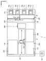
우선, 본 실시 형태에 따른 접합 시스템의 구성에 대해서 설명한다. 도 1은, 접합 시스템(1)의 구성의 개략을 도시하는 평면도이다. 도 2는, 접합 시스템(1)의 내부 구성의 개략을 도시하는 측면도이다.First, the structure of the bonding system which concerns on this embodiment is demonstrated. 1 : is a top view which shows the outline of the structure of the
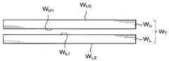
접합 시스템(1)에서는, 도 3에 도시한 바와 같이, 예를 들어 2매의 기판으로서의 웨이퍼(WU, WL)를 접합한다. 이하, 상측에 배치되는 웨이퍼를, 제1 기판으로서의 「상부 웨이퍼(WU)」라고 하고, 하측에 배치되는 웨이퍼를, 제2 기판으로서의 「하부 웨이퍼(WL)」라고 한다. 또한, 상부 웨이퍼(WU)가 접합되는 접합면을 「표면(WU1)」이라고 하고, 당해 표면(WU1)과 반대측의 면을 「이면(WU2)」이라고 한다. 마찬가지로, 하부 웨이퍼(WL)가 접합되는 접합면을 「표면(WL1)」이라고 하고, 당해 표면(WL1)와 반대측의 면을 「이면(WL2)」이라고 한다. 그리고, 접합 시스템(1)에서는, 상부 웨이퍼(WU)와 하부 웨이퍼(WL)를 접합하여, 중합 기판으로서의 중합 웨이퍼(WT)를 형성한다.In the
접합 시스템(1)은, 도 1에 도시한 바와 같이, 예를 들어 외부와의 사이에서 복수의 웨이퍼(WU, WL), 복수의 중합 웨이퍼(WT)를 각각 수용 가능한 카세트(CU, CL, CT)가 반출입되는 반출입 스테이션(2)과, 웨이퍼(WU, WL), 중합 웨이퍼(WT)에 대하여 소정의 처리를 실시하는 각종 처리 장치를 구비한 처리 스테이션(3)을 일체로 접속한 구성을 갖고 있다.As shown in FIG. 1 , the
반출입 스테이션(2)에는, 카세트 적재대(10)가 설치되어 있다. 카세트 적재대(10)에는, 복수, 예를 들어 4개의 카세트 적재판(11)이 설치되어 있다. 카세트 적재판(11)은, 수평 방향의 X 방향(도 1 중의 상하 방향)으로 일렬로 배열하여 배치되어 있다. 이들 카세트 적재판(11)에는, 접합 시스템(1)의 외부에 대하여 카세트(CU, CL, CT)를 반출입할 때 카세트(CU, CL, CT)를 적재할 수 있다. 이와 같이, 반출입 스테이션(2)은, 복수의 상부 웨이퍼(WU), 복수 하부 웨이퍼(WL), 복수의 중합 웨이퍼(WT)를 보유 가능하게 구성되어 있다. 또한, 카세트 적재판(11)의 개수는, 본 실시 형태에 한정되지 않고, 임의로 설정할 수 있다. 또한, 카세트의 하나를 이상 웨이퍼의 회수용으로서 사용해도 된다. 즉, 다양한 요인으로 상부 웨이퍼(WU)와 하부 웨이퍼(WL)와의 접합에 이상이 발생한 웨이퍼를, 다른 정상적인 중합 웨이퍼(WT)와 분리할 수 있는 카세트이다. 본 실시 형태에서는, 복수의 카세트(CT) 중, 1개의 카세트(CT)를 이상 웨이퍼의 회수용으로서 사용하고, 다른 카세트(CT)를 정상적인 중합 웨이퍼(WT)의 수용용으로서 사용하고 있다.In the carrying-in/
반출입 스테이션(2)에는, 카세트 적재대(10)에 인접해서 웨이퍼 반송부(20)가 설치되어 있다. 웨이퍼 반송부(20)에는, X 방향으로 연신되는 반송로(21) 상을 이동 가능한 웨이퍼 반송 장치(22)가 설치되어 있다. 웨이퍼 반송 장치(22)는, 연직 방향 및 연직축 둘레(θ 방향)로도 이동 가능하며, 각 카세트 적재판(11) 상의 카세트(CU, CL, CT)와, 후술하는 처리 스테이션(3)의 제3 처리 블록(G3)의 트랜지션 장치(50, 51)와의 사이에서 웨이퍼(WU, WL), 중합 웨이퍼(WT)를 반송할 수 있다.In the carrying-in/out
처리 스테이션(3)에는, 각종 장치를 구비한 복수, 예를 들어 3개의 처리 블록(G1, G2, G3)이 설치되어 있다. 예를 들어 처리 스테이션(3)의 정면측(도 1의 X 방향 부방향측)에는, 제1 처리 블록(G1)이 설치되고, 처리 스테이션(3)의 배면측(도 1의 X 방향 정방향측)에는, 제2 처리 블록(G2)이 설치되어 있다. 또한, 처리 스테이션(3)의 반출입 스테이션(2)측(도 1의 Y 방향 부방향측)에는, 제3 처리 블록(G3)이 설치되어 있다.The
예를 들어 제1 처리 블록(G1)에는, 웨이퍼(WU, WL)의 표면(WU1, WL1)을 개질하는 표면 개질 장치(30)가 배치되어 있다. 표면 개질 장치(30)에서는, 예를 들어 감압 분위기 하에서, 처리 가스인 산소 가스 또는 질소 가스가 여기되어 플라즈마화되어, 이온화된다. 이 산소 이온 또는 질소 이온이 표면(WU1, WL1)에 조사되어, 표면(WU1, WL1)이 플라즈마 처리되어, 개질된다.For example, in the first processing block G1 , a
예를 들어 제2 처리 블록(G2)에는, 예를 들어 순수에 의해 웨이퍼(WU, WL)의 표면(WU1, WL1)을 친수화함과 함께 당해 표면(WU1, WL1)을 세정하는 표면 친수화 장치(40), 웨이퍼(WU, WL)를 접합하는 접합 장치(41)가, 반출입 스테이션(2)측에서부터 이 순서로 수평 방향의 Y 방향으로 배열해서 배치되어 있다. 또한, 접합 장치(41)의 구성에 대해서는 후술한다.For example, in the second processing block G2, the surfaces WU1 and WL1 of the wafers WU and WL are hydrophilized with, for example, pure water, and the surfaces WU1 and WL1 are treated with water. The
표면 친수화 장치(40)에서는, 예를 들어 스핀 척에 유지된 웨이퍼(WU, WL)를 회전시키면서, 당해 웨이퍼(WU, WL) 상에 순수를 공급한다. 그렇게 하면, 공급된 순수는 웨이퍼(WU, WL)의 표면(WU1, WL1) 상을 확산하여, 표면(WU1, WL1)이 친수화된다.In the
예를 들어 제3 처리 블록(G3)에는, 도 2에 도시한 바와 같이 웨이퍼(WU, WL), 중합 웨이퍼(WT)의 트랜지션 장치(50, 51)가 아래부터 순서대로 2단으로 설치되어 있다.For example, in the third processing block G3, as shown in FIG. 2 , the
도 1에 도시한 바와 같이 제1 처리 블록(G1) 내지 제3 처리 블록(G3)에 둘러싸인 영역에는, 웨이퍼 반송 영역(60)이 형성되어 있다. 웨이퍼 반송 영역(60)에는, 예를 들어 웨이퍼 반송 장치(61)가 배치되어 있다.As shown in FIG. 1 , a
웨이퍼 반송 장치(61)는, 예를 들어 연직 방향, 수평 방향(Y 방향, X 방향) 및 연직축 둘레로 이동 가능한 반송 아암을 갖고 있다. 웨이퍼 반송 장치(61)는, 웨이퍼 반송 영역(60) 내를 이동하여, 주위의 제1 처리 블록(G1), 제2 처리 블록(G2) 및 제3 처리 블록(G3) 내의 소정의 장치에 웨이퍼(WU, WL), 중합 웨이퍼(WT)를 반송할 수 있다.The
이상의 접합 시스템(1)에는, 도 1에 도시한 바와 같이 제어부(70)가 설치되어 있다. 제어부(70)는, 예를 들어 컴퓨터이며, 프로그램 저장부(도시하지 않음)를 갖고 있다. 프로그램 저장부에는, 접합 시스템(1)에서의 웨이퍼(WU, WL), 중합 웨이퍼(WT)의 처리를 제어하는 프로그램이 저장되어 있다. 또한, 프로그램 저장부에는, 상술한 각종 처리 장치나 반송 장치 등의 구동계의 동작을 제어하여, 접합 시스템(1)에서의 후술하는 웨이퍼 접합 처리를 실현시키기 위한 프로그램도 저장되어 있다. 또한, 상기 프로그램은, 예를 들어 컴퓨터 판독 가능한 하드 디스크(HD), 플렉시블 디스크(FD), 콤팩트 디스크(CD), 마그넷 옵티컬 디스크(MO), 메모리 카드 등의 컴퓨터에 판독 가능한 기억 매체(H)에 기록되어 있던 것으로서, 그 기억 매체(H)로부터 제어부(70)에 인스톨된 것이어도 된다.In the
<2. 접합 장치의 구성><2. Configuration of splicing device>
이어서, 상술한 접합 장치(41)의 구성에 대해서 설명한다.Next, the structure of the
<2-1. 접합 장치의 전체 구성><2-1. Overall configuration of splicing device>
접합 장치(41)는, 도 4 및 도 5에 도시하는 바와 같이 내부를 밀폐 가능한 처리 용기(100)를 갖고 있다. 처리 용기(100)의 웨이퍼 반송 영역(60)측의 측면에는, 웨이퍼(WU, WL), 중합 웨이퍼(WT)의 반입출구(101)가 형성되고, 당해 반입출구(101)에는 개폐 셔터(102)가 설치되어 있다.The
처리 용기(100)의 내부는, 내벽(103)에 의해, 반송 영역(T1)과 처리 영역(T2)으로 구획되어 있다. 상술한 반입출구(101)는, 반송 영역(T1)에서의 처리 용기(100)의 측면에 형성되어 있다. 또한, 내벽(103)에도, 웨이퍼(WU, WL), 중합 웨이퍼(WT)의 반입출구(104)가 형성되어 있다.The inside of the
반송 영역(T1)의 Y 방향 정방향측에는, 웨이퍼(WU, WL), 중합 웨이퍼(WT)를 일시적으로 적재하기 위한 트랜지션(110)이 설치되어 있다. 트랜지션(110)은, 예를 들어 2단으로 형성되어, 웨이퍼(WU, WL), 중합 웨이퍼(WT) 중 2개를 동시에 적재할 수 있다.On the positive Y-direction side of the transfer region T1 , a
반송 영역(T1)에는, 웨이퍼 반송 기구(111)가 설치되어 있다. 웨이퍼 반송 기구(111)는, 예를 들어 연직 방향, 수평 방향(X 방향, Y 방향) 및 연직축 둘레로 이동 가능한 반송 아암을 갖고 있다. 그리고, 웨이퍼 반송 기구(111)는, 반송 영역(T1) 내, 또는 반송 영역(T1)과 처리 영역(T2)과의 사이에서 웨이퍼(WU, WL), 중합 웨이퍼(WT)를 반송할 수 있다.A
반송 영역(T1)의 Y 방향 부방향측에는, 웨이퍼(WU, WL)의 수평 방향의 배향을 조절하는 위치 조절 기구(120)가 설치되어 있다. 위치 조절 기구(120)는, 웨이퍼(WU, WL)를 유지해서 회전시키는 유지부(도시하지 않음)를 구비한 베이스(121)와, 웨이퍼(WU, WL)의 노치부의 위치를 검출하는 검출부(122)를 갖고 있다. 그리고, 위치 조절 기구(120)에서는, 베이스(121)에 유지된 웨이퍼(WU, WL)를 회전시키면서 검출부(122)에서 웨이퍼(WU, WL)의 노치부의 위치를 검출함으로써, 당해 노치부의 위치를 조절해서 웨이퍼(WU, WL)의 수평 방향의 배향을 조절하고 있다. 또한, 베이스(121)에 있어서 웨이퍼(WU, WL)를 유지하는 구조는 특별히 한정되는 것이 아니라, 예를 들어 핀 척 구조나 스핀 척 구조 등, 다양한 구조가 사용된다.A
또한, 반송 영역(T1)에는, 상부 웨이퍼(WU)의 표리면을 반전시키는 반전 기구(130)가 설치되어 있다. 반전 기구(130)는, 상부 웨이퍼(WU)를 유지하는 유지 아암(131)을 갖고 있다. 유지 아암(131)은, 수평 방향(X 방향)으로 연신되어 있다. 또한 유지 아암(131)에는, 상부 웨이퍼(WU)를 유지하는 유지 부재(132)가, 예를 들어 4군데에 설치되어 있다.In addition, in the transfer region T1 , a reversing
유지 아암(131)은, 예를 들어 모터 등을 구비한 구동부(133)에 지지되어 있다. 이 구동부(133)에 의해, 유지 아암(131)은 수평축을 중심으로 회동 가능하다. 또한 유지 아암(131)은, 구동부(133)를 중심으로 회동 가능함과 함께, 수평 방향(X 방향)으로 이동 가능하다. 구동부(133)의 하방에는, 예를 들어 모터 등을 구비한 다른 구동부(도시하지 않음)가 설치되어 있다. 그 밖의 구동부에 의해, 구동부(133)는 연직 방향으로 연신되는 지지 기둥(134)을 따라 연직 방향으로 이동할 수 있다. 이렇게 구동부(133)에 의해, 유지 부재(132)에 유지된 상부 웨이퍼(WU)는, 수평축을 중심으로 회동할 수 있음과 함께 연직 방향 및 수평 방향으로 이동할 수 있다. 또한, 유지 부재(132)에 유지된 상부 웨이퍼(WU)는, 구동부(133)를 중심으로 회동하여, 위치 조절 기구(120)로부터 후술하는 상부 척(140)과의 사이를 이동할 수 있다.The holding
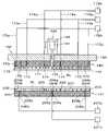
처리 영역(T2)에는, 상부 웨이퍼(WU)를 하면에서 흡착 유지하는 제1 유지부로서의 상부 척(140)과, 하부 웨이퍼(WL)를 상면에서 적재해서 흡착 유지하는 제2 유지부로서의 하부 척(141)이 설치되어 있다. 하부 척(141)은, 상부 척(140)의 하방에 설치되어, 상부 척(140)과 대향 배치 가능하게 구성되어 있다. 즉, 상부 척(140)에 유지된 상부 웨이퍼(WU)와 하부 척(141)에 유지된 하부 웨이퍼(WL)는, 대향해서 배치 가능하게 되어 있다.In the processing region T2 , the
상부 척(140)은, 당해 상부 척(140)의 상방에 설치된 상부 척 유지부(150)에 유지되어 있다. 상부 척 유지부(150)는, 처리 용기(100)의 천장면에 설치되어 있다. 즉, 상부 척(140)은, 상부 척 유지부(150)를 개재해서 처리 용기(100)에 고정되어 설치되어 있다.The
상부 척 유지부(150)에는, 하부 척(141)에 유지된 하부 웨이퍼(WL)의 표면(WL1)을 촬상하는 상부 촬상부(151)가 설치되어 있다. 즉, 상부 촬상부(151)는 상부 척(140)에 인접해서 설치되어 있다. 상부 촬상부(151)에는, 예를 들어 CCD 카메라가 사용된다.The upper
하부 척(141)은, 당해 하부 척(141)의 하방에 설치된 하부 척 스테이지(160)에 지지되어 있다. 하부 척 스테이지(160)에는, 상부 척(140)에 유지된 상부 웨이퍼(WU)의 표면(WU1)을 촬상하는 하부 촬상부(161)가 설치되어 있다. 즉, 하부 촬상부(161)는 하부 척(141)에 인접해서 설치되어 있다. 하부 촬상부(161)에는, 예를 들어 CCD 카메라가 사용된다.The
하부 척 스테이지(160)는, 당해 하부 척 스테이지(160)의 하방에 설치된 제1 하부 척 이동부(162)에 지지되고, 또한 제1 하부 척 이동부(162)는, 지지대(163)에 지지되어 있다. 제1 하부 척 이동부(162)는, 후술하는 바와 같이 하부 척(141)을 수평 방향(X 방향)으로 이동시키도록 구성되어 있다. 또한, 제1 하부 척 이동부(162)는, 하부 척(141)을 연직 방향으로 이동 가능하면서, 또한 연직축을 중심으로 회전 가능하게 구성되어 있다.The
지지대(163)는, 당해 지지대(163)의 하면측에 설치되고, 수평 방향(X 방향)으로 연신되는 한 쌍의 레일(164, 164)에 설치되어 있다. 그리고, 지지대(163)는, 제1 하부 척 이동부(162)에 의해 레일(164)을 따라 이동 가능하게 구성되어 있다. 또한, 제1 하부 척 이동부(162)는, 예를 들어 레일(164)을 따라 설치된 리니어 모터(도시하지 않음)에 의해 이동한다.The
한 쌍의 레일(164, 164)은, 제2 하부 척 이동부(165)에 배치되어 있다. 제2 하부 척 이동부(165)는, 당해 제2 하부 척 이동부(165)의 하면측에 설치되고, 수평 방향(Y 방향)으로 연신되는 한 쌍의 레일(166, 166)에 설치되어 있다. 그리고, 제2 하부 척 이동부(165)는, 레일(166)을 따라 이동 가능하게 구성되어, 즉 하부 척(141)을 수평 방향(Y 방향)으로 이동시키도록 구성되어 있다. 제2 하부 척 이동부(165)는, 예를 들어 레일(166)을 따라 설치된 리니어 모터(도시하지 않음)에 의해 이동한다. 한 쌍의 레일(166, 166)은, 처리 용기(100)의 저면에 설치된 적재대(167) 상에 배치되어 있다.The pair of
<2-2. 상부 척의 구성><2-2. Configuration of upper chuck>
이어서, 접합 장치(41)의 상부 척(140)의 상세한 구성에 대해서 설명한다.Next, the detailed structure of the
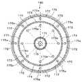
상부 척(140)에는, 도 6 및 도 7에 도시하는 바와 같이 핀 척 방식이 채용되어 있다. 상부 척(140)은, 평면에서 볼 때 상부 웨이퍼(WU)의 직경 이상의 직경을 갖는 본체부(170)를 갖고 있다. 본체부(170)의 하면에는, 상부 웨이퍼(WU)의 이면(WU2)에 접촉하는 복수의 핀(171)이 설치되어 있다. 또한, 도 7에서는, 핀(171)의 도시를 생략하고 있다.The
또한, 본체부(170)의 하면에는, 상부 웨이퍼(WU)를 진공화해서 흡착하는 복수의 흡인부(172 내지 174)가 설치되어 있다. 흡인부(172 내지 174)는, 각각 핀(171)과 동일한 높이를 갖고, 상부 웨이퍼(WU)의 이면(WU2)에 접촉한다.Further, on the lower surface of the
제1 흡인부(172)는, 평면에서 볼 때 원호 형상을 갖고 있다. 제1 흡인부(172)는, 본체부(170)의 외주부에 있어서, 당해 본체부(170)와 동심 원주 상에 복수, 예를 들어 8개, 둘레 방향으로 배열하여 소정의 간격을 두고 배치되어 있다.The
이들 8개의 제1 흡인부(172)에는, 각각 제1 흡인 관(172a)을 통해서, 제1 진공 펌프(172b)가 접속되어 있다. 제1 진공 펌프(172b)에 의한 진공화에 의해, 8개의 제1 흡인부(172)는, 개별로 상부 웨이퍼(WU)를 흡착할 수 있다.A
제2 흡인부(173)는, 제1 흡인부(172)와 마찬가지로, 평면에서 볼 때 원호 형상을 갖고 있다. 제2 흡인부(173)는, 제1 흡인부(172)보다도 본체부(170)의 내주측에 있어서, 당해 본체부(170)와 동심 원주 상에 복수, 예를 들어 8개, 둘레 방향으로 배열하여 소정의 간격을 두고 배치되어 있다. 또한, 제1 흡인부(172)의 중심부와 제2 흡인부(173)의 중심부는, 본체부(170)의 중심선 상에 배치되어 있다.The
이들 8개의 제2 흡인부(173)에는, 각각 제2 흡인관(173a)을 통해서, 제2 진공 펌프(173b)가 접속되어 있다. 제2 진공 펌프(173b)에 의한 진공화에 의해, 8개의 제2 흡인부(173)는 개별로 상부 웨이퍼(WU)를 흡착할 수 있다.A
제3 흡인부(174)는, 평면에서 볼 때 원환 형상을 갖고 있다. 제3 흡인부(174)는, 제2 흡인부(173)보다도 본체부(170)의 내주측에 있어서, 당해 본체부(170)와 동심 원주 상에 배치되어 있다. 제3 흡인부(174)에는, 제3 흡인관(174a)을 통해서, 제3 진공 펌프(174b)가 접속되어 있다. 제3 진공 펌프(174b)에 의한 진공화에 의해, 제3 흡인부(174)는 상부 웨이퍼(WU)를 흡착할 수 있다.The
본체부(170)에는, 당해 본체부(170)로부터 상부 웨이퍼(WU)의 이탈을 검출하는 기판 검출부로서의 센서(175)가 설치되어 있다. 센서(175)는, 제1 흡인부(172)와 제2 흡인부(173)의 사이에서, 본체부(170)와 동심 원주 상에 복수, 예를 들어 8개, 둘레 방향으로 배열하여 소정의 간격을 두고 배치되어 있다. 즉, 센서(175), 제1 흡인부(172)의 중심부 및 제2 흡인부(173)의 중심부는, 본체부(170)의 동일 중심선 상에 배치되어 있다. 또한, 이들 센서(175)의 종류나 배치 등의 상세에 대해서는 후술한다.A
본체부(170)의 중심부에는, 당해 본체부(170)를 두께 방향으로 관통하는 관통 구멍(176)이 형성되어 있다. 이 본체부(170)의 중심부는, 상부 척(140)에 흡착 유지되는 상부 웨이퍼(WU)의 중심부에 대응하고 있다. 그리고 관통 구멍(176)에는, 후술하는 압동 부재(190)에서의 액추에이터부(191)의 선단부가 삽입 관통하도록 되어 있다.A through
<2-3. 상부 척의 센서의 상세><2-3. Details of the sensor of the upper chuck>
이어서, 상술한 센서(175)의 상세, 및 당해 센서(175)의 검사 결과를 사용한 흡인부(172 내지 174)의 제어 방법에 대해서 설명한다.Next, the detail of the
후술하는 바와 같이 상부 웨이퍼(WU)와 하부 웨이퍼(WL)를 접합할 때는, 우선, 상부 웨이퍼(WU)의 중심부를 밀어 내려서 하부 웨이퍼(WL)의 중심부에 접촉시켜, 상부 웨이퍼(WU)의 중심부와 하부 웨이퍼(WL)의 중심부가 분자간력에 의해 접합됨으로써 양쪽 웨이퍼의 중심부에 접합 영역이 형성된다. 그 후, 접합 영역이 양쪽 웨이퍼(WU, WL)의 중심부로부터 외주부를 향해서 확대되는 본딩 웨이브가 발생하여, 상부 웨이퍼(WU) 및 하부 웨이퍼(WL)의 표면(WU1, WL1)끼리가 전체면에서 접합된다.As will be described later, when bonding the upper wafer WU and the lower wafer WL , first, push down the center of the upper wafer WU and contact the center of the lower wafer WL , and the upper wafer ( A bonding region is formed in the central portion of both wafers by bonding the central portion of WU and the central portion of the lower wafer WL by intermolecular force. After that, a bonding wave is generated in which the bonding region is expanded from the center to the outer periphery of both wafers WU and WL , and the surfaces WU1 and WL1 of the upper wafer WU and the lower wafer WL . ) are joined on the entire surface.
센서(175)는, 이 본딩 웨이브를 파악하기 위해서, 본체부(170)에 설치되어 있다.The
센서(175)로는, 다양한 센서를 사용할 수 있다. 예를 들어 센서(175)로는, 반사식의 파이버 센서를 사용해도 된다. 이러한 경우, 센서(175)로부터 상부 웨이퍼(WU)를 향해서 광을 발하고, 또한 센서(175)에 있어서 그 반사광을 수광해서 수광량을 측정한다. 그리고, 이 반사광의 수광량을 측정함으로써, 광축과 상부 웨이퍼(WU)와의 직교도를 파악할 수 있다. 즉, 반사광량이 작은 경우, 광축과 상부 웨이퍼(WU)와의 직교도가 커서(상부 웨이퍼(WU)의 기울기가 커서), 상부 웨이퍼(WU)는 상부 척(140)으로부터 이탈하고 있지만, 하부 웨이퍼(WL)와 맞닿지 않은 상태를 의미하고 있다. 한편, 반사광량이 큰 경우, 광축과 상부 웨이퍼(WU)와의 직교도가 작아(상부 웨이퍼(WU)의 기울기가 작아), 상부 웨이퍼(WU)가 상부 척(140)로부터 이탈하여, 하부 웨이퍼(WL)에 맞닿아 있는 상태를 의미하고 있다. 따라서, 센서(175)로 반사광량을 측정함으로써, 당해 센서(175)에서의 상부 웨이퍼(WU)와 하부 웨이퍼(WL)의 맞닿음 상태(환언하면, 상부 척(140)로부터 상부 웨이퍼(WU)의 이탈 상태)를 검출할 수 있어, 본딩 웨이브를 파악할 수 있다.As the
또한, 예를 들어 센서(175)에는, 정전 용량 센서 또는 거리 측장 센서를 사용해도 된다. 정전 용량 센서를 사용하는 경우, 상부 웨이퍼(WU)와의 정전 용량을 측정함으로써, 상부 척(140)과 상부 웨이퍼(WU)와의 거리를 측정할 수 있다. 또한, 거리 측장 센서를 사용하는 경우, 센서(175)로부터 상부 웨이퍼(WU)에 레이저광을 발하고, 센서(175)에서 그 반사광을 수광함으로써 상부 척(140)과 상부 웨이퍼(WU)와의 거리를 측정할 수 있다. 이렇게 상부 척(140)과 상부 웨이퍼(WU)와의 거리를 측정함으로써, 당해 센서(175)에서의 상부 웨이퍼(WU)와 하부 웨이퍼(WL)의 맞닿음 상태(환언하면, 상부 척(140)으로부터 상부 웨이퍼(WU)의 이탈 상태)를 검출할 수 있어, 본딩 웨이브를 파악할 수 있다.Note that, for example, a capacitive sensor or a distance measuring sensor may be used as the
또한, 예를 들어 센서(175)에는, 유체 센서를 사용해도 된다. 이러한 경우, 본체부(170)에는 흡착 패드(도시하지 않음)가 설치되고, 즉 도 6 및 도 7에 도시하는 부호 「175」의 위치에는 흡착 패드가 설치되고, 센서(175)는 이 흡착 패드에 접속되는 흡인관(도시하지 않음)에 설치되어 있다. 또한, 흡착 패드는, 상부 웨이퍼(WU)를 흡착해서 유지하는 것을 목적으로 하는 것이 아니라, 본딩 웨이브에 영향을 미치지 않을 정도의 미소한 압력, 예를 들어 -10kPa 정도로 상부 웨이퍼(WU)를 진공화한다. 그리고, 센서(175)는, 각 흡인관을 흐르는 기체의 유량 또는 압력을 측정한다. 예를 들어 상부 척(140)으로부터 상부 웨이퍼(WU)가 이탈한 경우, 흡인관 내의 기체의 흐름이 바뀌고, 그 기체의 유량 및 압력이 변화한다. 센서(175)는, 이 흡인관 내의 기류의 변화를 측정하여, 상부 척(140)으로부터 상부 웨이퍼(WU)의 이탈(환언하면, 상부 웨이퍼(WU)와 하부 웨이퍼(WL)의 맞닿음 상태)을 검출할 수 있어, 본딩 웨이브를 파악할 수 있다. 또한, 센서(175)는, 제1 흡인부(172)의 제1 흡인관(172a) 및 제2 흡인부(173)의 제2 흡인관(173a)에 각각 설치되어 있어도 된다.Note that, for example, a fluid sensor may be used as the
이러한 센서(175)는, 상술한 바와 같이 제1 흡인부(172)와 제2 흡인부(173)의 사이에서, 본체부(170)와 동심 원주 상에 둘레 방향으로 배열하여 소정의 간격을 두고 배치되어 있다. 이어서, 이 센서(175)의 배치에 대해서 설명한다.These
센서(175)의 배치는, 상부 웨이퍼(WU)의 물성, 예를 들어 영률이나 포와송비 등의 이방성에 따라서 결정된다. 도 8은, 종래에 있어서의 웨이퍼간의 접합 영역의 확대 모습을 도시하는 설명도이다. 본 발명자들은, 도 8에 도시한 바와 같이, 접합 처리를 행할 때, 접합 영역(A)이 동심원 형상이 아니라, 불균일하게 확대되는 것을 지견하였다. 또한, 도 8은, 상부 척(140)에 유지된 상부 웨이퍼(WU)를 하방에서 본 평면도이다.The arrangement of the
상부 웨이퍼(WU)는, 표면(WU1)과 수직인 방향에서의 결정 방향이 [100]인 단결정 실리콘 웨이퍼이다. 상부 웨이퍼(WU)의 노치부(N)는, 상부 웨이퍼(WU)의 [011] 결정 방향의 외연에 형성된다. 그리고, 접합 영역(A)은, 상부 웨이퍼(WU)의 중심부로부터 상부 웨이퍼(WU)의 표면(WU1)에 대하여 평행인 [0-11] 결정 방향을 향하는 방향을 기준으로 하는 90° 주기의 방향(도 8에 도시하는 0°, 90°, 180°, 270°의 방향이며, 이하, 90° 방향이라고 하는 경우가 있음)과 비교하여, 상부 웨이퍼(WU)의 중심부로부터 상부 웨이퍼(WU)의 표면(WU1)에 대하여 평행인 [010] 결정 방향을 향하는 방향을 기준으로 하는 45° 주기의 방향(도 8에 도시하는 45°, 135°, 225°, 315°의 방향, 이하, 45° 방향이라고 하는 경우가 있음)으로 빠르게 확대된다. 그 결과, 접합 개시 시(중심부 접합 시)에 원 형상이었던 접합 영역(A)의 형상은, 확대됨에 따라서 45° 방향을 정점으로 하는 사각형에 가까워지게 된다.The upper wafer WU is a single crystal silicon wafer whose crystal direction in a direction perpendicular to the surface WU1 is [100]. [011] The notch N of the upper wafer WU is formed on the outer edge of the upper wafer WU in the crystal direction. And, the junction region A is 90° from the central portion of the upper wafer WU toward the [0-11] crystal direction parallel to the surface WU1 of the upper wafer WU as a reference. Compared with the direction of the period (the directions of 0°, 90°, 180°, and 270° shown in FIG. 8 , which may be referred to as the 90° direction hereinafter), the upper wafer from the center of the upper wafer WU The direction of the 45° period with respect to the direction toward the [010] crystal direction parallel to the surface (WU1 ) of (WU ) (the directions of 45°, 135°, 225°, 315° shown in FIG. 8 ) , hereinafter sometimes referred to as the 45° direction). As a result, the shape of the bonding area|region A which was circular at the time of bonding start (at the time of center bonding) becomes close to the rectangle which makes a 45 degree direction a vertex as it expands.
본 실시 형태에서는, 센서(175)가 본체부(170)와 동심 원주 상에 8개 설치되고, 즉 90° 방향과 45° 방향에 설치되어 있다. 따라서, 이들 센서(175)를 사용해서 상부 척(140)으로부터 상부 웨이퍼(WU)의 이탈을 검출하여, 도 8에 나타낸 접합 영역(A)을 검출함으로써, 본딩 웨이브를 파악할 수 있다.In the present embodiment, eight
이러한 센서(175)의 검출 결과는, 제어부(70)에 출력된다. 제어부(70)에서는, 센서(175)의 검출 결과에 기초하여, 흡인부(172 내지 174)의 동작을 제어한다.The detection result of the
도 9는, 센서(175)의 검출 결과의 일례를 나타내는 그래프이다. 도 9의 횡축은, 접합 처리의 경과 시간을 나타내고, 종축은, 센서(175)의 검출 결과, 즉 상부 척(140)에 대한 상부 웨이퍼(WU)의 위치를 나타내고 있다. 센서(175)의 검출 결과가 P1(상부 척(140)에 대하여 상부 웨이퍼(WU)가 가까운)인 경우, 당해 센서(175)의 위치에서 상부 웨이퍼(WU)는 상부 척(140)에 맞닿아 있고, 접합 영역(A)이 도달하지 않은 것을 나타내고 있다. 센서(175)의 검출 결과가 P2(상부 척(140)에 대하여 상부 웨이퍼(WU)가 먼)인 경우, 당해 센서(175)의 위치에서 상부 웨이퍼(WU)는 상부 척(140)으로부터 이격되어, 하부 웨이퍼(WL)와 맞닿아 있고, 접합 영역(A)이 도달한 것을 나타내고 있다.9 is a graph showing an example of the detection result of the
도 9의 (a)는 도 8에 도시한 바와 같이 접합 영역(A)이 불균일, 즉 대략 사각 형상으로 확대되는 경우를 나타내고 있다. 상술한 바와 같이 접합 영역(A)은, 90° 방향과 비교해서 45° 방향에서 빠르게 확대된다. 이 때문에, 45° 방향에서 접합 영역(A)이 도달하는 타이밍과, 90° 방향에서 접합 영역(A)이 도달하는 타이밍의 시간차(ΔT)는 커진다.Fig. 9(a) shows a case in which the junction region A is non-uniform, that is, expanded in a substantially rectangular shape as shown in Fig. 8 . As described above, the bonding region A is rapidly expanded in the 45° direction compared to the 90° direction. For this reason, the time difference ΔT between the timing at which the bonding region A arrives in the 45° direction and the timing at which the bonding region A arrives in the 90° direction becomes large.
그래서, 제어부(70)에서는, 접합 영역(A)의 확대를 균일하게 하기 위해서, 도 9의 (b)에 도시하는 바와 같이 시간차(ΔT)가 소정의 역치 내에 들어가도록 제어한다. 여기서, 시간차(ΔT)와 접합 후의 중합 웨이퍼(WT)의 왜곡과의 사이에는 상관이 있다. 상기 ΔT의 소정의 역치는, 이 중합 웨이퍼(WT)의 왜곡의 허용 범위로부터 설정된다.Then, in the
제어부(70)에서의 제어는, 구체적으로 45° 방향에서의 제2 흡인부(173)가 상부 웨이퍼(WU)를 떼어 놓는 타이밍을 늦게 하고, 90° 방향에서의 제2 흡인부(173)가 상부 웨이퍼(WU)를 떼어 놓는 타이밍을 빠르게 한다. 이에 의해, 8개의 센서(175)의 위치에서, 접합 영역(A)이 도달하는 타이밍을 거의 동일하게 할 수 있다. 따라서, 접합 영역(A)의 확대를 균일하게 해서, 본딩 웨이브를 균일하게(동심원 형상에 가까운 형상으로) 할 수 있다.Specifically, the control by the
또한, 본 실시 형태에서는, 센서(175)의 검출 결과에 기초하여 제2 흡인부(173)의 흡착 타이밍을 제어하는 경우에 대해서 설명했지만, 제2 흡인부(173)의 흡착력을 더 제어해도 된다. 또한, 센서(175)의 검출 결과에 기초하여, 다른 흡인부(172, 174)를 제어해도 된다.In addition, although this embodiment demonstrated the case where the adsorption|suction timing of the
<2-4. 상부 척 유지부의 구성><2-4. Configuration of the upper chuck holding part>
이어서, 접합 장치(41)의 상부 척 유지부(150)의 상세한 구성에 대해서 설명한다.Next, the detailed structure of the upper
상부 척 유지부(150)는, 도 5에 도시하는 바와 같이 상부 척(140)의 본체부(170)의 상면에 설치된 상부 척 스테이지(180)를 갖고 있다. 상부 척 스테이지(180)는, 평면에서 볼 때 적어도 본체부(170)의 상면을 덮도록 설치되고, 또한 본체부(170)에 대하여, 예를 들어 나사 고정에 의해 고정되어 있다. 상부 척 스테이지(180)는, 처리 용기(100)의 천장면에 설치된 복수의 지지 부재(181)에 지지되어 있다.The upper
상부 척 스테이지(180)의 상면에는, 도 6에 도시하는 바와 같이 상부 웨이퍼(WU)의 중심부를 가압하는 압동 부재(190)가 더 설치되어 있다. 압동 부재(190)는, 액추에이터부(191)와 실린더부(192)를 갖고 있다.On the upper surface of the
액추에이터부(191)는, 전공 레귤레이터(도시하지 않음)로부터 공급되는 공기에 의해 일정 방향으로 일정한 압력을 발생시키는 것으로, 압력의 작용점의 위치에 관계없이 당해 압력을 일정하게 발생시킬 수 있다. 그리고, 전공 레귤레이터로부터의 공기에 의해, 액추에이터부(191)는, 상부 웨이퍼(WU)의 중심부와 맞닿아서 당해 상부 웨이퍼(WU)의 중심부에 걸리는 가압 하중을 제어할 수 있다. 또한, 액추에이터부(191)의 선단부는, 전공 레귤레이터로부터의 공기에 의해, 관통 구멍(176)을 삽입 관통해서 연직 방향으로 승강 가능하게 되어 있다.The
액추에이터부(191)는, 실린더부(192)에 지지되어 있다. 실린더부(192)는, 예를 들어 모터를 내장한 구동부에 의해 액추에이터부(191)를 연직 방향으로 이동시킬 수 있다.The
이상과 같이 압동 부재(190)는, 액추에이터부(191)에 의해 가압 하중의 제어를 하고, 실린더부(192)에 의해 액추에이터부(191)의 이동의 제어를 하고 있다. 그리고, 압동 부재(190)는, 후술하는 웨이퍼(WU, WL)의 접합 시에, 상부 웨이퍼(WU)의 중심부와 하부 웨이퍼(WL)의 중심부를 맞닿게 해서 가압할 수 있다.As described above, the pressing
<2-5. 하부 척의 구성><2-5. Configuration of lower chuck>
이어서, 접합 장치(41)의 하부 척(141)의 상세한 구성에 대해서 설명한다.Next, the detailed structure of the
하부 척(141)에는, 도 6에 도시하는 바와 같이 상부 척(140)과 마찬가지로 핀 척 방식이 채용되어 있다. 하부 척(141)은, 평면에서 볼 때 하부 웨이퍼(WL)의 직경 이상의 직경을 갖는 본체부(200)를 갖고 있다. 본체부(200)의 상면에는, 하부 웨이퍼(WL)의 이면(WL2)에 접촉하는 복수의 핀(201)이 설치되어 있다. 또한, 본체부(200)의 상면의 외주부에는, 핀(201)과 동일한 높이를 갖고, 하부 웨이퍼(WL)의 이면(WL2)의 외주부를 지지하는 외측 리브(202)가 설치되어 있다. 외측 리브(202)는, 복수의 핀(201)의 외측에 환상으로 설치되어 있다.As shown in FIG. 6 , a pin chuck method is employed for the
또한, 본체부(200)의 상면에는, 외측 리브(202)의 내측에서, 핀(201)과 동일한 높이를 갖고, 하부 웨이퍼(WL)의 이면(WL2)을 지지하는 내측 리브(203)가 설치되어 있다. 내측 리브(203)는, 외측 리브(202)와 동심원 형상으로 환상으로 설치되어 있다. 그리고, 외측 리브(202)의 내측 영역(204)(이하, 흡인 영역(204)이라고 하는 경우가 있음)은, 내측 리브(203)의 내측의 제1 흡인 영역(204a)과, 내측 리브(203)의 외측의 제2 흡인 영역(204b)으로 구획되어 있다.In addition, on the upper surface of the
본체부(200)의 상면에는, 제1 흡인 영역(204a)에 있어서, 하부 웨이퍼(WL)를 진공화하기 위한 제1 흡인구(205a)가 형성되어 있다. 제1 흡인구(205a)는, 예를 들어 제1 흡인 영역(204a)에서 1군데에 형성되어 있다. 제1 흡인구(205a)에는, 본체부(200)의 내부에 설치된 제1 흡인관(206a)이 접속되어 있다. 또한 제1 흡인 관(206a)에는, 제1 진공 펌프(207a)가 접속되어 있다.A
또한, 본체부(200)의 상면에는, 제2 흡인 영역(204b)에 있어서, 하부 웨이퍼(WL)를 진공화하기 위한 제2 흡인구(205b)가 형성되어 있다. 제2 흡인구(205b)는, 예를 들어 제2 흡인 영역(204b)에서 2군데에 형성되어 있다. 제2 흡인구(205b)에는, 본체부(200)의 내부에 설치된 제2 흡인관(206b)이 접속되어 있다. 또한, 제2 흡인관(206b)에는, 제2 진공 펌프(207b)가 접속되어 있다.Further, on the upper surface of the
그리고, 하부 웨이퍼(WL), 본체부(200) 및 외측 리브(202)에 둘러싸여 형성된 흡인 영역(204a, 204b)을 각각 흡인구(205a, 205b)로부터 진공화하여, 흡인 영역(204a, 204b)을 감압한다. 이때, 흡인 영역(204a, 204b)의 외부의 분위기가 대기압이기 때문에, 하부 웨이퍼(WL)는, 감압된 분만큼 대기압에 의해 흡인 영역(204a, 204b)측으로 눌려, 하부 척(141)에 하부 웨이퍼(WL)가 흡착 유지된다. 또한, 하부 척(141)은, 제1 흡인 영역(204a)과 제2 흡인 영역(204b)마다 하부 웨이퍼(WL)를 진공화 가능하게 구성되어 있다.Then, the
하부 척(141)에 있어서, 본체부(200)의 중심부 부근에는, 당해 본체부(200)를 두께 방향으로 관통하는 관통 구멍(도시하지 않음)이, 예를 들어 3군데에 형성되어 있다. 그리고 관통 구멍에는, 제1 하부 척 이동부(162)의 하방에 설치된 승강 핀이 삽입 관통하게 되어 있다.In the
본체부(200)의 외주부에는, 웨이퍼(WU, WL), 중합 웨이퍼(WT)가 하부 척(141)으로부터 튀어나오거나, 미끄러져 떨어지는 것을 방지하는 가이드 부재(도시하지 않음)가 설치되어 있다. 가이드 부재는, 본체부(200)의 외주부에 복수 개소, 예를 들어 4군데에 등간격으로 설치되어 있다.A guide member (not shown) for preventing the wafers WU , WL , and the polymerization wafer WT from protruding from the
또한, 접합 장치(41)에서의 각 부의 동작은, 상술한 제어부(70)에 의해 제어된다.In addition, the operation|movement of each part in the
<3. 접합 처리 방법><3. Joint processing method>
이어서, 이상과 같이 구성된 접합 시스템(1)을 사용해서 행하여지는 웨이퍼(WU, WL)의 접합 처리 방법에 대해서 설명한다. 도 10은, 이러한 웨이퍼 접합 처리의 주된 공정의 예를 나타내는 흐름도이다.Next, the bonding processing method of the wafers WU and WL performed using the
우선, 복수매의 상부 웨이퍼(WU)를 수용한 카세트(CU), 복수매의 하부 웨이퍼(WL)를 수용한 카세트(CL), 및 빈 카세트(CT)가, 반출입 스테이션(2)의 소정의 카세트 적재판(11)에 적재된다. 그 후, 웨이퍼 반송 장치(22)에 의해 카세트(CU) 내의 상부 웨이퍼(WU)가 취출되어, 처리 스테이션(3)의 제3 처리 블록(G3)의 트랜지션 장치(50)에 반송된다.First, a cassette (CU ) accommodating a plurality of upper wafers (WU ), a cassette (CL ) accommodating a plurality of lower wafers (WL ), and an empty cassette (CT ) are It is loaded on the predetermined
다음으로 상부 웨이퍼(WU)는, 웨이퍼 반송 장치(61)에 의해 제1 처리 블록(G1)의 표면 개질 장치(30)에 반송된다. 표면 개질 장치(30)에서는, 소정의 감압 분위기 하에서, 처리 가스인 산소 가스 또는 질소 가스가 여기되어 플라즈마화되어, 이온화된다. 이 산소 이온 또는 질소 이온이 상부 웨이퍼(WU)의 표면(WU1)에 조사되어, 당해 표면(WU1)이 플라즈마 처리된다. 그리고, 상부 웨이퍼(WU)의 표면(WU1)이 개질된다(도 10의 공정 S1).Next, the upper wafer WU is transferred to the
다음으로 상부 웨이퍼(WU)는, 웨이퍼 반송 장치(61)에 의해 제2 처리 블록(G2)의 표면 친수화 장치(40)에 반송된다. 표면 친수화 장치(40)에서는, 스핀 척에 유지된 상부 웨이퍼(WU)를 회전시키면서, 당해 상부 웨이퍼(WU) 상에 순수를 공급한다. 그렇게 하면, 공급된 순수는 상부 웨이퍼(WU)의 표면(WU1) 상을 확산하여, 표면 개질 장치(30)에서 개질된 상부 웨이퍼(WU)의 표면(WU1)에 수산기(실라놀기)가 부착되어 당해 표면(WU1)이 친수화된다. 또한, 당해 순수에 의해, 상부 웨이퍼(WU)의 표면(WU1)이 세정된다(도 10의 공정 S2).Next, the upper wafer WU is transferred to the
다음으로 상부 웨이퍼(WU)는, 웨이퍼 반송 장치(61)에 의해 제2 처리 블록(G2)의 접합 장치(41)에 반송된다. 접합 장치(41)에 반입된 상부 웨이퍼(WU)는, 트랜지션(110)을 통해서 웨이퍼 반송 기구(111)에 의해 위치 조절 기구(120)에 반송된다. 그리고, 위치 조절 기구(120)에 의해, 상부 웨이퍼(WU)의 수평 방향의 배향이 조절된다(도 10의 공정 S3).Next, the upper wafer WU is transferred to the
그 후, 위치 조절 기구(120)로부터 반전 기구(130)의 유지 아암(131)에 상부 웨이퍼(WU)가 수수된다. 계속해서 반송 영역(T1)에서, 유지 아암(131)을 반전시킴으로써, 상부 웨이퍼(WU)의 표리면이 반전된다(도 10의 공정 S4). 즉, 상부 웨이퍼(WU)의 표면(WU1)이 하방으로 향하게 된다.Thereafter, the upper wafer WU is transferred from the
그 후, 반전 기구(130)의 유지 아암(131)이, 구동부(133)를 중심으로 회동해서 상부 척(140)의 하방으로 이동한다. 그리고, 반전 기구(130)로부터 상부 척(140)에 상부 웨이퍼(WU)가 수수된다. 상부 웨이퍼(WU)는, 상부 척(140)에 그 이면(WU2)이 흡착 유지된다(도 10의 공정 S5). 구체적으로는, 진공 펌프(172b, 173b, 174b)를 작동시켜, 흡인부(172, 173, 174)에서 상부 웨이퍼(WU)를 진공화하여, 상부 웨이퍼(WU)가 상부 척(140)에 흡착 유지된다.Thereafter, the holding
상부 웨이퍼(WU)에 상술한 공정 S1 내지 S5의 처리가 행하여지고 있는 동안에, 당해 상부 웨이퍼(WU)에 이어서 하부 웨이퍼(WL)의 처리가 행하여진다. 우선, 웨이퍼 반송 장치(22)에 의해 카세트(CL) 내의 하부 웨이퍼(WL)가 취출되어, 처리 스테이션(3)의 트랜지션 장치(50)에 반송된다.While the processing of steps S1 to S5 described above is being performed on the upper wafer WU , the processing of the lower wafer WL is performed following the upper wafer WU . First, the lower wafer WL in the cassetteCL is taken out by the
다음으로 하부 웨이퍼(WL)는, 웨이퍼 반송 장치(61)에 의해 표면 개질 장치(30)에 반송되어, 하부 웨이퍼(WL)의 표면(WL1)이 개질된다(도 10의 공정 S6). 또한, 공정 S6에서의 하부 웨이퍼(WL)의 표면(WL1)의 개질은, 상술한 공정 S1과 마찬가지이다.Next, the lower wafer WL is transferred to the
그 후, 하부 웨이퍼(WL)는, 웨이퍼 반송 장치(61)에 의해 표면 친수화 장치(40)에 반송되어, 하부 웨이퍼(WL)의 표면(WL1)이 친수화됨과 함께 당해 표면(WL1)이 세정된다(도 10의 공정 S7). 또한, 공정 S7에서의 하부 웨이퍼(WL)의 표면(WL1)의 친수화 및 세정은, 상술한 공정 S2와 마찬가지이다.Thereafter, the lower wafer WL is transferred to the
그 후, 하부 웨이퍼(WL)는, 웨이퍼 반송 장치(61)에 의해 접합 장치(41)에 반송된다. 접합 장치(41)에 반입된 하부 웨이퍼(WL)는, 트랜지션(110)을 통해서 웨이퍼 반송 기구(111)에 의해 위치 조절 기구(120)에 반송된다. 그리고, 위치 조절 기구(120)에 의해, 하부 웨이퍼(WL)의 수평 방향의 배향이 조절된다(도 10의 공정 S8).Thereafter, the lower wafer WL is transferred to the
그 후, 하부 웨이퍼(WL)는, 웨이퍼 반송 기구(111)에 의해 하부 척(141)에 반송되고, 하부 척(141)에 그 이면(WL2)이 흡착 유지된다(도 10의 공정 S9). 구체적으로는, 진공 펌프(207a, 207b)를 작동시켜, 흡인 영역(204a, 204b)에서 흡인구(205a, 205b)를 통해서 하부 웨이퍼(WL)를 진공화하여, 하부 웨이퍼(WL)가 하부 척(141)에 흡착 유지된다.Thereafter, the lower wafer WL is transferred to the
이어서, 상부 척(140)에 유지된 상부 웨이퍼(WU)와 하부 척(141)에 유지된 하부 웨이퍼(WL)와의 수평 방향의 위치 조절을 행한다. 구체적으로는, 제1 하부 척 이동부(162)와 제2 하부 척 이동부(165)에 의해 하부 척(141)을 수평 방향(X 방향 및 Y 방향)으로 이동시키고, 상부 촬상부(151)를 사용하여, 하부 웨이퍼(WL)의 표면(WL1) 상의 미리 정해진 기준점을 순차적으로 촬상한다. 동시에, 하부 촬상부(161)를 사용하여, 상부 웨이퍼(WU)의 표면(WU1) 상의 미리 정해진 기준점을 순차적으로 촬상한다. 촬상된 화상은, 제어부(70)에 출력된다. 제어부(70)에서는, 상부 촬상부(151)에서 촬상된 화상과 하부 촬상부(161)에서 촬상된 화상에 기초하여, 상부 웨이퍼(WU)의 기준점과 하부 웨이퍼(WL)의 기준점이 각각 합치하는 위치에, 제1 하부 척 이동부(162)와 제2 하부 척 이동부(165)에 의해 하부 척(141)을 이동시킨다. 이렇게 해서 상부 웨이퍼(WU)와 하부 웨이퍼(WL)의 수평 방향 위치가 조절된다(도 10의 공정 S10).Next, the horizontal position of the upper wafer WU held by the
또한, 공정 S10에서는, 상술한 바와 같이 하부 척(141)을 수평 방향으로 이동시킴과 함께, 제1 하부 척 이동부(162)에 의해 하부 척(141)을 회전시켜, 당해 하부 척(141)의 회전 방향 위치(하부 척(141)의 방향)도 조절된다.Further, in step S10 , as described above, the
그 후, 제1 하부 척 이동부(162)에 의해 하부 척(141)을 연직 상방으로 이동시켜, 상부 척(140)과 하부 척(141)의 연직 방향 위치의 조절을 행하고, 당해 상부 척(140)에 유지된 상부 웨이퍼(WU)와 하부 척(141)에 유지된 하부 웨이퍼(WL)와의 연직 방향 위치의 조절을 행한다(도 10의 공정 S11). 또한, 하부 웨이퍼(WL)의 표면(WL1)과 상부 웨이퍼(WU)의 표면(WU1)과의 간격은 소정의 거리, 예를 들어 50㎛ 내지 200㎛로 조절된다. 그리고, 도 11에 도시하는 바와 같이 상부 웨이퍼(WU)와 하부 웨이퍼(WL)가 소정의 위치에 대향 배치된다.Thereafter, the
이어서, 상부 척(140)에 유지된 상부 웨이퍼(WU)와 하부 척(141)에 유지된 하부 웨이퍼(WL)의 접합 처리가 행하여진다.Next, bonding processing of the upper wafer WU held by the
또한, 본 실시 형태에서는, 상술한 바와 같이 본딩 웨이브가 균일해지도록, 미리 제2 흡인부(173)의 흡착 타이밍이 설정되어 있는 경우에 대해서 설명한다. 즉, 예를 들어 전 로트의 상부 웨이퍼(WU)에 대하여 센서(175)에 의해 접합 영역(A)의 확대를 검출하고, 그 검출 결과에 기초하여, 금회 로트의 상부 웨이퍼(WU)에 대한, 제2 흡인부(173)의 흡착 타이밍이 설정되고 있다.In addition, this embodiment demonstrates the case where the adsorption|suction timing of the
우선, 도 12에 도시하는 바와 같이 압동 부재(190)의 실린더부(192)에 의해 액추에이터부(191)를 하강시킨다. 그렇게 하면, 이 액추에이터부(191)의 하강에 수반하여, 상부 웨이퍼(WU)의 중심부가 가압되어 하강한다. 이때, 전공 레귤레이터로부터 공급되는 공기에 의해, 액추에이터부(191)에는, 소정의 가압 하중이 걸린다. 그리고, 압동 부재(190)에 의해, 상부 웨이퍼(WU)의 중심부와 하부 웨이퍼(WL)의 중심부를 맞닿게 해서 가압한다(도 10의 공정 S12).First, as shown in FIG. 12 , the
공정 S13에서는, 제1 진공 펌프(172b)의 동작을 정지하고, 제1 흡인부(172)로부터 상부 웨이퍼(WU)의 진공화를 정지함과 함께, 제2 진공 펌프(173b) 및 제3 진공 펌프(174b)는 작동시킨 채 그대로 두고, 제2 흡인부(173) 및 제3 흡인부(174)에서 상부 웨이퍼(WU)를 진공화한다.In step S13 , the operation of the
상부 웨이퍼(WU)의 중심부와 하부 웨이퍼(WL)의 중심부를 맞닿게 해서 가압하면, 당해 중심부의 사이에 접합이 개시된다. 즉, 상부 웨이퍼(WU)의 표면(WU1)과 하부 웨이퍼(WL)의 표면(WL1)은 각각 공정 S1, S6에서 개질되어 있기 때문에, 우선, 표면(WU1, WL1)간에 반데르발스힘(분자간력)이 발생하여, 당해 표면(WU1, WL1)끼리가 접합된다. 또한, 상부 웨이퍼(WU)의 표면(WU1)과 하부 웨이퍼(WL)의 표면(WL1)은 각각 공정 S2, S7에서 친수화되어 있기 때문에, 표면(WU1, WL1)간의 친수기가 수소 결합해서(분자간력), 표면(WU1, WL1)끼리가 견고하게 접합된다. 이와 같이 하여, 접합 영역(A)이 형성된다.When the central portion of the upper wafer WU and the central portion of the lower wafer WL are pressed against each other, bonding is started between the central portions. That is, since the surface WU1 of the upper wafer WU and the surface WL1 of the lower wafer WL are modified in steps S1 and S6, respectively, first, between the surfaces WU1 and WL1 A van der Waals force (intermolecular force) is generated, and the surfaces WU1 and WL1 are joined to each other. In addition, since the surface WU1 of the upper wafer WU and the surface WL1 of the lower wafer WL are hydrophilized in steps S2 and S7, respectively, hydrophilic groups between the surfaces WU1 and WL1 hydrogen bonds (intermolecular force), and the surfaces (WU1 , WL1 ) are firmly bonded to each other. In this way, the bonding region A is formed.
그 후, 상부 웨이퍼(WU)와 하부 웨이퍼(WL)와의 사이에서는, 상부 웨이퍼(WU) 및 하부 웨이퍼(WL)의 중심부로부터 외주부를 향해서 접합 영역(A)이 확대되어 가는 본딩 웨이브가 발생한다.Thereafter, between the upper wafer WU and the lower wafer WL , the bonding wave in which the bonding area A expands from the center of the upper wafer WU and the lower wafer WL toward the outer periphery. occurs
도 13에 도시하는 바와 같이 압동 부재(190)에 의해 상부 웨이퍼(WU)의 중심부와 하부 웨이퍼(WL)의 중심부를 가압한 상태에서 제2 진공 펌프(173b)의 작동을 정지하고, 제2 흡인부(173)로부터 상부 웨이퍼(WU)의 진공화를 정지한다. 이때, 상술한 바와 같이 8개의 제2 흡인부(173)의 흡착 타이밍을 상이하게 한다. 즉, 45° 방향에서의 제2 흡인부(173)가 상부 웨이퍼(WU)를 떼어 놓는 타이밍을 늦게 하고, 90° 방향에서의 제2 흡인부(173)가 상부 웨이퍼(WU)를 떼어 놓는 타이밍을 빠르게 한다. 이에 의해 8개의 센서(175)의 위치에서, 접합 영역(A)이 도달하는 타이밍을 거의 동일하게 할 수 있어, 본딩 웨이브를 균일하게 할 수 있다.13, the operation of the
또한 도 14에 도시한 바와 같이, 제3 진공 펌프(174b)의 작동을 정지하고, 제3 흡인부(174)로부터 상부 웨이퍼(WU)의 진공화를 정지한다. 그리고, 상부 웨이퍼(WU)가 하부 웨이퍼(WL) 상에 순차적으로 낙하해서 맞닿고, 상술한 표면(WU1, WL1)간의 반데르발스힘과 수소 결합에 의한 접합이 순차적으로 넓어진다. 이렇게 해서, 상부 웨이퍼(WU)의 표면(WU1)과 하부 웨이퍼(WL)의 표면(WL1)이 전체면에서 맞닿아, 상부 웨이퍼(WU)와 하부 웨이퍼(WL)가 접합된다(도 10의 공정 S13). 이때, 본딩 웨이브가 균일하게 되어 있으므로, 접합된 중합 웨이퍼(WT)의 왜곡(디스토션)을 억제할 수 있다.14 , the operation of the
또한, 공정 S13에서는, 8개의 센서(175)를 사용해서 접합 영역(A)을 검출하고, 본딩 웨이브를 모니터링하여, 상부 웨이퍼(WU)와 하부 웨이퍼(WL)의 접합 상태를 검사한다. 상술한 바와 같이 본 실시 형태에서는, 미리 본딩 웨이브가 균일해지도록 제2 흡인부(173)의 흡착 타이밍이 설정되어 있지만, 다양한 외란에 의해 본딩 웨이브가 불균일해지는 경우가 있다. 이러한 경우에는, 경고를 발함으로써, 제품의 수율을 향상시킬 수 있다. 또한, 이와 같이 본딩 웨이브가 불균일해지는 경우, 센서(175)의 검출 결과에 기초하여, 후속하는 상부 웨이퍼(WU)와 하부 웨이퍼(WL)를 접합할 때의, 제2 흡인부(173)의 흡착 타이밍을 보정한다.Further, in step S13 , the bonding region A is detected using the eight
그 후, 도 15에 도시하는 바와 같이 압동 부재(190)의 액추에이터부(191)를 상부 척(140)까지 상승시킨다. 또한, 진공 펌프(207a, 207b)의 작동을 정지하여, 흡인 영역(204)에서의 하부 웨이퍼(WL)의 진공화를 정지하여, 하부 척(141)에 의한 하부 웨이퍼(WL)의 흡착 유지를 정지한다.Thereafter, as shown in FIG. 15 , the
상부 웨이퍼(WU)와 하부 웨이퍼(WL)가 접합된 중합 웨이퍼(WT)는, 웨이퍼 반송 장치(61)에 의해 트랜지션 장치(51)에 반송되고, 그 후 반출입 스테이션(2)의 웨이퍼 반송 장치(22)에 의해 소정의 카세트 적재판(11)의 카세트(CT)에 반송된다. 이렇게 해서, 일련의 웨이퍼(WU, WL)의 접합 처리가 종료된다.The superposed wafer WT in which the upper wafer WU and the lower wafer WL are bonded is transferred to the
이상의 실시 형태에 의하면, 센서(175)에 의해, 상부 척(140)에 유지된 상부 웨이퍼(WU)가, 당해 상부 척(140)으로부터 이탈하는 것을 검출할 수 있어, 본딩 웨이브를 파악할 수 있다. 그리고, 제어부(70)에서는, 센서(175)의 검출 결과에 기초하여, 제2 흡인부(173)의 흡착 타이밍을 제어한다. 이에 의해, 본딩 웨이브를 균일하게 할 수 있어, 중합 웨이퍼(WT)의 왜곡을 억제할 수 있다.According to the above embodiment, by the
또한, 본 실시 형태의 접합 시스템(1)은, 표면 개질 장치(30), 표면 친수화 장치(40) 및 접합 장치(41)를 구비하고 있으므로, 하나의 시스템 내에서 웨이퍼(WU, WL)의 접합을 효율적으로 행할 수 있다. 따라서, 웨이퍼 접합 처리의 스루풋을 향상시킬 수 있다.In addition, since the
<4. 다른 실시 형태><4. Another embodiment>
이어서, 본 발명의 다른 실시 형태에 대해서 설명한다.Next, another embodiment of the present invention will be described.
이상의 실시 형태의 상부 척(140)에 있어서, 센서(175)는 제1 흡인부(172)와 제2 흡인부(173)의 사이에서, 본체부(170)와 동심 원주 상에 둘레 방향으로 배열하여 소정의 간격을 두고 배치되어 있었지만, 센서(175)의 배치는 이것에 한정되지 않는다.In the
도 16에 도시하는 바와 같이 센서(175)는, 제1 흡인부(172)와 제2 흡인부(173)의 사이 외에도, 또한 제2 흡인부(173)보다도 본체부(170)의 내주측에서, 본체부(170)와 동심 원주 상에 복수, 예를 들어 8개, 둘레 방향으로 배열하여 소정의 간격을 두고 배치되어 있어도 된다. 즉, 2개의 센서(175), 제1 흡인부(172)의 중심부 및 제2 흡인부(173)의 중심부는, 본체부(170)의 동일 중심선 상에 배치되어 있다. 또한, 이하에서는, 제1 흡인부(172)와 제2 흡인부(173)의 사이의 센서(175)를 센서(175a)라고 하고, 제2 흡인부(173)의 내주측의 센서(175)를 센서(175b)라고 한다.As shown in FIG. 16 , the
이러한 경우, 센서(175b)의 검출 결과에 기초하여, 당해 센서(175b)와 동일 중심선 상에 있는 제2 흡인부(173)의 흡착 타이밍을 제어할 수 있다. 따라서, 제2 흡인부(173)를 실시간으로 피드 포워드 제어할 수 있어, 본딩 웨이브를 보다 확실하고 균일하게 할 수 있다.In this case, the adsorption timing of the
또한, 센서(175a)를 생략하고, 센서(175b)만을 설치해도 된다. 단, 센서(175a)는, 본체부(170)의 중심부로부터 이격되어 배치되어 있기 때문에, 센서(175b)에 비해 접합 영역(A)의 불균일 확산을 현저하게 파악할 수 있다. 구체적으로는, 예를 들어 상부 웨이퍼(WU)의 직경이 300mm인 경우, 센서(175a)는, 본체부(170)의 중심부로부터 직경 240mm보다 외측에 배치되어 있는 것이 바람직하다.In addition, the
또한, 도 8에 도시한 바와 같이, 종래에 있어서의 접합 영역(A)은 대략 사각 형상으로 확대된다. 이 접합 영역(A)의 확대의 대칭성을 고려하면, 센서(175)의 수를 적게 하는 것도 가능하다.Moreover, as shown in FIG. 8, the bonding area|region A in the prior art is enlarged in a substantially rectangular shape. Considering the symmetry of the expansion of the junction region A, it is also possible to reduce the number of
예를 들어 도 17의 (a) 내지 (b)에 도시하는 바와 같이 2개의 센서(175)를 본체부(170)의 원주 상에 일렬로 배치해도 된다. 즉, 적어도 45° 방향과 90° 방향으로 각각 1개의 센서(175)가 배치되어 있으면 된다. 이러한 경우, 45° 방향의 센서(175)를 사용하여, 다른 45° 방향의 접합 영역(A)의 확대를 추측할 수 있고, 또한 90° 방향의 센서(175)를 사용하여, 다른 90° 방향의 접합 영역(A)의 확대를 추측할 수 있다.For example, as shown in FIGS. 17A to 17B , two
단, 도 7에 도시한 바와 같이 센서(175)를 본체부(170)의 원주 상의 전체 둘레에 걸쳐서 설치한 경우, 상부 웨이퍼(WU)와 하부 웨이퍼(WL)의 사이의 간격의 대소까지 파악할 수 있다. 여기서, 상부 웨이퍼(WU)와 하부 웨이퍼(WL)는 엄밀하게는 평행이 아니라, 미소한 거리, 예를 들어 수 ㎛ 기울어져 있는 경우가 있다. 이러한 경우, 상부 웨이퍼(WU)와 하부 웨이퍼(WL)의 간격이 큰 쪽이 공기가 외부로 빠지기 더 쉽기 때문에, 접합 영역(A)이 빨리 확대된다. 이렇게 접합 영역(A)의 확대에 차가 있어도, 센서(175)가 본체부(170)의 전체 둘레에 설치되어 있으면, 본딩 웨이브를 적절하게 파악할 수 있다.However, as shown in FIG. 7 , when the
이상의 실시 형태에서는, 센서(175)를 사용해서 상부 웨이퍼(WU)와 하부 웨이퍼(WL)의 맞닿음 상태를 검출하여, 본딩 웨이브를 파악하고 있었지만, 또한 액추에이터부(191)의 변위를 측정하여, 본딩 웨이브를 파악해도 된다. 도 19에 도시하는 바와 같이 압동 부재(190)에는, 레이저 변위계(300)가 설치되어 있다. 레이저 변위계(300)는, 액추에이터부(191)에 설치된 타깃(301)의 변위를 측정하여, 당해 액추에이터부(191)의 변위를 측정한다.In the above embodiment, the contact state between the upper wafer WU and the lower wafer WL is detected using the
이러한 경우, 상기 실시 형태의 공정 S12(도 12)에서, 압동 부재(190)의 액추에이터부(191)를 하강시킬 때, 레이저 변위계(300)에 의해 액추에이터부(191)의 변위를 측정한다. 그리고, 이 레이저 변위계(300)로 측정된 변위가 소정의 역치에 달했을 때, 상부 웨이퍼(WU)의 중심부와 하부 웨이퍼(WL)의 중심부가 맞닿은 것을 검출한다.In this case, in step S12 ( FIG. 12 ) of the embodiment, when the
이렇게 레이저 변위계(300)에 의한 측정 결과에 기초하여, 접합 영역(A)의 개시를 파악할 수 있으므로, 본딩 웨이브를 보다 적절하게 파악할 수 있다. 또한, 레이저 변위계(300)에 의한 측정 결과에 기초하여, 흡인부(172 내지 174)의 흡착 타이밍을 제어하는 것도 가능하게 된다.Thus, based on the measurement result by the
또한, 압동 부재(190)에 설치되는 변위계는, 레이저 변위계(300)에 한정되지 않고, 액추에이터부(191)의 변위를 측정할 수 있는 것이라면 임의로 선택할 수 있다.In addition, the displacement gauge provided in the
이상의 실시 형태의 상부 척(140)에 있어서, 8개의 제2 흡인부(173)의 각각에는 하나의 제2 진공 펌프(173b)가 접속되어 있었지만, 복수의 제2 진공 펌프(173b)가 복수의 제2 흡인부(173)의 동작을 그룹 단위로 제어해도 된다. 예를 들어 4개의 45° 방향에 있는 제1 그룹의 제2 흡인부(173)를, 1개의 제2 진공 펌프(173b)로 제어해도 된다. 또한, 4개의 90° 방향에 있는 제2 그룹의 제2 흡인부(173)를, 다른 제2 진공 펌프(173b)로 제어해도 된다.In the
마찬가지로, 8개의 제1 흡인부(172)에 대해서도, 복수의 제1 진공 펌프(172b)가 복수의 제1 흡인부(172)의 동작을 그룹 단위로 제어해도 된다.Similarly, also about the eight
또한, 흡인부(172 내지 174)의 수나 배치는, 도 7에 나타낸 예에 한정되지 않는다. 본체부(170)에 있어서 동일 원주 상의 흡인부의 수는, 8개 이외이어도 된다. 또한, 본체부(170)에 있어서, 흡인부는 3중 이상으로 설치되어 있어도 된다.In addition, the number and arrangement|positioning of the suction parts 172-174 are not limited to the example shown in FIG. In the
이상의 실시 형태의 접합 장치(41)에서는, 하부 척(141)이 수평 방향으로 이동 가능하게 구성되어 있었지만, 상부 척(140)을 수평 방향으로 이동 가능하게 구성해도 되고, 또는 상부 척(140)과 하부 척(141)을 모두 수평 방향으로 이동 가능하게 구성해도 된다.In the
또한, 이상의 실시 형태의 접합 장치(41)에서는, 하부 척(141)이 연직 방향으로 이동 가능하게 구성되어 있었지만, 상부 척(140)을 연직 방향으로 이동 가능하게 구성해도 되고, 또는 상부 척(140)과 하부 척(141)을 모두 연직 방향으로 이동 가능하게 구성해도 된다.In addition, in the
또한, 이상의 실시 형태의 접합 장치(41)에서는, 하부 척(141)이 회전 가능하게 구성되어 있었지만, 상부 척(140)을 회전 가능하게 구성해도 되고, 또는 상부 척(140)과 하부 척(141)을 모두 회전 가능하게 구성해도 된다.In addition, in the
이상의 실시 형태의 접합 시스템(1)에 있어서, 접합 장치(41)에서 웨이퍼(WU, WL)를 접합한 후, 접합된 중합 웨이퍼(WT)를 소정의 온도에서 더 가열(어닐 처리)해도 된다. 중합 웨이퍼(WT)에 이러한 가열 처리를 행함으로써, 접합 계면을 보다 견고하게 결합시킬 수 있다.In the
이상, 첨부 도면을 참조하면서 본 발명의 적합한 실시 형태에 대해서 설명했지만, 본 발명은 이러한 예에 한정되지 않는다. 당업자라면 특허 청구 범위에 기재된 사상의 범주 내에서, 각종 변경예 또는 수정예에 상도할 수 있음은 명확하며, 그들에 대해서도 당연히 본 발명의 기술적 범위에 속하는 것이라고 이해된다. 본 발명은 이 예에 한하지 않고 다양한 형태를 채용할 수 있는 것이다. 본 발명은, 기판이 웨이퍼 이외의 FPD(플랫 패널 디스플레이), 포토마스크용 마스크 레티클 등의 다른 기판인 경우에도 적용할 수 있다.As mentioned above, although preferred embodiment of this invention was described referring an accompanying drawing, this invention is not limited to this example. It is clear that a person skilled in the art can imagine various changes or modifications within the scope of the spirit described in the claims, and it is understood that they naturally fall within the technical scope of the present invention. The present invention is not limited to this example, and various forms can be adopted. The present invention can also be applied to a case where the substrate is another substrate other than a wafer, such as an FPD (flat panel display) and a mask reticle for a photomask.
1 : 접합 시스템 2 : 반출입 스테이션
3 : 처리 스테이션 30 : 표면 개질 장치
40 : 표면 친수화 장치 41 : 접합 장치
61 : 웨이퍼 반송 장치 70 : 제어부
140 : 상부 척 141 : 하부 척
172 : 제1 흡인부 173 : 제2 흡인부
174 : 제3 흡인부 175 : 센서
190 : 압동 부재 300 : 레이저 변위계
WU : 상부 웨이퍼 WL : 하부 웨이퍼
WT : 중합 웨이퍼1: junction system 2: carry-in/out station
3: processing station 30: surface modification device
40: surface hydrophilization device 41: bonding device
61: wafer transfer device 70: control unit
140: upper chuck 141: lower chuck
172: first suction unit 173: second suction unit
174: third suction unit 175: sensor
190: pressure member 300: laser displacement meter
WU : upper wafer WL : lower wafer
WT : polymerization wafer
Claims (18)
Translated fromKorean하면에 제1 기판을 진공화해서 흡착 유지하는 제1 유지부와,
상기 제1 유지부의 하방에 설치되고, 상면에 제2 기판을 진공화해서 흡착 유지하는 제2 유지부와,
상기 제1 유지부에 설치되고, 상기 제1 기판의 중심부를 가압하는 압동 부재와,
상기 제1 유지부에 설치되고, 당해 제1 유지부로부터의 상기 제1 기판의 이탈을 검출하는 복수의 기판 검출부를 갖고,
상기 복수의 기판 검출부는 각각, 당해 기판 검출부에 대응하는 위치에 있어서의 상기 제1 유지부로부터의 제1 기판의 이탈을 검출하는, 접합 장치.A bonding apparatus for bonding substrates to each other, comprising:
a first holding part for vacuuming and adsorbing and holding the first substrate on the lower surface;
a second holding part installed below the first holding part and vacuuming and adsorbing and holding the second substrate on the upper surface;
a pressing member installed in the first holding unit and pressing the central portion of the first substrate;
a plurality of substrate detection units provided in the first holding unit and configured to detect detachment of the first substrate from the first holding unit;
The bonding apparatus, wherein each of the plurality of substrate detection units detects detachment of the first substrate from the first holding unit at a position corresponding to the substrate detection unit.
상기 복수의 기판 검출부는, 상기 제1 기판에 광을 조사하고, 당해 제1 기판으로부터 반사된 반사광의 수광량을 측정하는, 접합 장치.According to claim 1,
The bonding apparatus, wherein the plurality of substrate detection units irradiate light to the first substrate and measure the amount of light received of reflected light reflected from the first substrate.
상기 복수의 기판 검출부는, 상기 제1 기판과의 사이의 정전 용량을 측정하는, 접합 장치.According to claim 1,
The bonding apparatus, wherein the plurality of substrate detection units measure an electrostatic capacitance between the plurality of substrates and the first substrate.
상기 복수의 기판 검출부는, 상기 제1 유지부와 상기 제1 기판과의 거리를 측정하는, 접합 장치.According to claim 1,
The bonding apparatus, wherein the plurality of substrate detection units measure a distance between the first holding unit and the first substrate.
상기 복수의 기판 검출부는, 상기 제1 유지부와 동심원 관계로 당해 제1 유지부에 설치되어 있는, 접합 장치.5. The method according to any one of claims 1 to 4,
The bonding apparatus, wherein the plurality of substrate detection units are provided in the first holding unit in a concentric relationship with the first holding unit.
상기 복수의 기판 검출부는, 상기 제1 유지부의 복수의 원주 중의 적어도 하나 상에 설치되어 있는, 접합 장치.6. The method of claim 5,
The bonding apparatus in which the said some board|substrate detection part is provided on at least one of the some circumference|surroundings of the said 1st holding part.
상기 제1 유지부는, 상기 제1 기판에 접촉하여, 당해 제1 기판을 진공화해서 흡착하는 복수의 흡인부를 포함하고,
상기 접합 장치는, 상기 복수의 기판 검출부의 검출 결과에 기초하여, 상기 복수의 흡인부를 제어하는 제어부를 더 포함하는, 접합 장치.5. The method according to any one of claims 1 to 4,
The first holding unit includes a plurality of suction units that are in contact with the first substrate to vacuum and adsorb the first substrate,
The bonding apparatus further includes a control unit configured to control the plurality of suction units based on the detection results of the plurality of substrate detection units.
상기 제어부는, 상기 복수의 기판 검출부 중의 하나가 상기 제1 기판의 이탈을 검출하는 타이밍과, 상기 복수의 기판 검출부 중의 다른 것이 상기 제1 기판의 이탈을 검출하는 타이밍과의 시간차를 산출하고, 당해 시간차가 미리 결정된 역치 내로 되도록 상기 복수의 흡인부를 제어하는, 접합 장치.8. The method of claim 7,
The control unit calculates a time difference between a timing at which one of the plurality of substrate detection units detects detachment of the first substrate and a timing at which the other of the plurality of substrate detecting units detects detachment of the first substrate, The bonding apparatus which controls the said some suction part so that a time difference may become within a predetermined threshold value.
상기 압동 부재의 변위를 측정하는 변위계를 더 포함하는, 접합 장치.5. The method according to any one of claims 1 to 4,
The bonding apparatus further comprising a displacement meter for measuring the displacement of the pressing member.
상기 접합 장치를 구비한 처리 스테이션과,
상기 제1 기판, 상기 제2 기판 또는 상기 제1 기판과 상기 제2 기판이 접합된 중합 기판을 각각 복수 보유하고, 또한 상기 처리 스테이션에 대하여 상기 제1 기판, 상기 제2 기판 또는 상기 중합 기판을 반출입하는 반출입 스테이션을 포함하고,
상기 처리 스테이션은,
상기 제1 기판 또는 상기 제2 기판이 접합되는 표면을 개질하는 표면 개질 장치와,
상기 표면 개질 장치에서 개질된 상기 제1 기판 또는 상기 제2 기판의 표면을 친수화하는 표면 친수화 장치와,
상기 표면 개질 장치, 상기 표면 친수화 장치 및 상기 접합 장치에 대하여 상기 제1 기판, 상기 제2 기판 또는 상기 중합 기판을 반송하기 위한 반송 장치를 포함하고,
상기 접합 장치에서는, 상기 표면 친수화 장치에서 표면이 친수화된 상기 제1 기판과 상기 제2 기판을 접합하는, 접합 시스템.A bonding system provided with the bonding apparatus in any one of Claims 1-4,
a processing station provided with the bonding device;
Each of the first substrate, the second substrate, or a plurality of polymerized substrates to which the first and second substrates are bonded is held, and the first substrate, the second substrate or the polymerized substrate is provided with respect to the processing station. Including a carry-in/out station for carrying in and out,
the processing station,
a surface modification device for modifying a surface to which the first substrate or the second substrate is bonded;
a surface hydrophilization device for hydrophilizing the surface of the first substrate or the second substrate modified in the surface modification device;
a transport device for transporting the first substrate, the second substrate, or the polymerized substrate with respect to the surface modification device, the surface hydrophilization device, and the bonding device;
In the bonding apparatus, the bonding system is for bonding the first substrate and the second substrate whose surface has been made hydrophilic in the surface hydrophilization apparatus.
제1 유지부의 하면에 유지된 제1 기판과 제2 유지부의 상면에 유지된 제2 기판을 대향 배치하는 배치 공정과,
그 후, 상기 제1 유지부에 설치되고, 상기 제1 기판의 중심부를 가압하는 압동 부재를 하강시켜, 당해 압동 부재에 의해 상기 제1 기판의 중심부와 상기 제2 기판의 중심부를 가압해서 맞닿게 하는 가압 공정과,
그 후, 상기 제1 기판의 중심부와 상기 제2 기판의 중심부가 맞닿은 상태에서, 상기 제1 기판의 중심부로부터 외주부를 향해서, 상기 제1 기판과 상기 제2 기판을 순차적으로 접합하는 접합 공정을 포함하고,
상기 접합 공정에서, 상기 제1 유지부에 설치된 복수의 기판 검출부 각각에 의해, 당해 기판 검출부에 대응하는 위치에 있어서의 상기 제1 유지부로부터의 상기 제1 기판의 이탈을 검출하여, 접합 처리의 상태를 검사하는, 접합 방법.A bonding method for bonding substrates to each other, comprising:
a disposing step of opposingly disposing the first substrate held on the lower surface of the first holding unit and the second substrate held on the upper surface of the second holding unit;
Thereafter, the pressure member provided in the first holding unit for pressing the center portion of the first substrate is lowered, and the center portion of the first substrate and the center portion of the second substrate are pressed and brought into contact with the pressure member by the pressure member. a pressurizing process,
Thereafter, in a state in which the central portion of the first substrate and the central portion of the second substrate are in contact with each other, from the central portion of the first substrate toward the outer peripheral portion, a bonding process of sequentially bonding the first substrate and the second substrate is included. do,
In the bonding step, the separation of the first substrate from the first holding unit at a position corresponding to the substrate detection unit is detected by each of the plurality of substrate detection units provided in the first holding unit, and the bonding process is performed. A bonding method to check the condition.
상기 복수의 기판 검출부는, 상기 제1 기판에 광을 조사하여, 당해 제1 기판으로부터 반사된 반사광의 수광량을 측정하는, 접합 방법.12. The method of claim 11,
The bonding method, wherein the plurality of substrate detection units irradiate the first substrate with light and measure the amount of light received of reflected light reflected from the first substrate.
상기 복수의 기판 검출부는, 상기 제1 기판과의 사이의 정전 용량을 측정하는, 접합 방법.12. The method of claim 11,
The bonding method, wherein the plurality of substrate detection units measure an electrostatic capacitance between the plurality of substrates and the first substrate.
상기 복수의 기판 검출부는, 상기 제1 유지부와 상기 제1 기판과의 거리를 측정하는, 접합 방법.12. The method of claim 11,
The bonding method, wherein the plurality of substrate detection units measure a distance between the first holding unit and the first substrate.
상기 제1 유지부는, 상기 제1 기판에 접촉하여, 당해 제1 기판을 진공화해서 흡착하는 복수의 흡인부를 포함하고,
상기 복수의 기판 검출부의 검출 결과에 기초하여, 상기 복수의 흡인부를 제어하는, 접합 방법.12. The method of claim 11,
The first holding unit includes a plurality of suction units that are in contact with the first substrate to vacuum and adsorb the first substrate,
The bonding method of controlling the plurality of suction portions based on detection results of the plurality of substrate detection portions.
상기 복수의 기판 검출부 중의 하나가 상기 제1 기판의 이탈을 검출하는 타이밍과, 상기 복수의 기판 검출부 중의 다른 것이 상기 제1 기판의 이탈을 검출하는 타이밍과의 시간차를 산출하고, 당해 시간차가 미리 결정된 역치 내로 되도록 상기 복수의 흡인부를 제어하는, 접합 방법.16. The method of claim 15,
A time difference between the timing at which one of the plurality of substrate detection units detects the detachment of the first substrate and the timing at which the other of the plurality of substrate detecting units detect the detachment of the first substrate is calculated, and the time difference is determined in advance. The joining method which controls the said some suction part so that it may become within a threshold value.
상기 접합 공정에서, 변위계에 의해 상기 압동 부재의 변위를 더 측정하고, 상기 변위계에 의한 측정 결과와 상기 복수의 기판 검출부에 의한 검출 결과에 기초하여, 접합 처리의 상태를 검사하는, 접합 방법.15. The method according to any one of claims 11 to 14,
In the bonding step, the displacement of the pressure member is further measured by a displacement meter, and the state of the bonding process is inspected based on the measurement result by the displacement meter and the detection result by the plurality of substrate detection units.
Priority Applications (1)
| Application Number | Priority Date | Filing Date | Title |
|---|---|---|---|
| KR1020220119814AKR102651554B1 (en) | 2016-12-01 | 2022-09-22 | Bonding apparatus, bonding system, bonding method and computer storage medium |
Applications Claiming Priority (2)
| Application Number | Priority Date | Filing Date | Title |
|---|---|---|---|
| JPJP-P-2016-233985 | 2016-12-01 | ||
| JP2016233985AJP6820189B2 (en) | 2016-12-01 | 2016-12-01 | Joining equipment, joining systems, joining methods, programs and computer storage media |
Related Child Applications (1)
| Application Number | Title | Priority Date | Filing Date |
|---|---|---|---|
| KR1020220119814ADivisionKR102651554B1 (en) | 2016-12-01 | 2022-09-22 | Bonding apparatus, bonding system, bonding method and computer storage medium |
Publications (2)
| Publication Number | Publication Date |
|---|---|
| KR20180062948A KR20180062948A (en) | 2018-06-11 |
| KR102447744B1true KR102447744B1 (en) | 2022-09-28 |
Family
ID=62243444
Family Applications (3)
| Application Number | Title | Priority Date | Filing Date |
|---|---|---|---|
| KR1020170159511AActiveKR102447744B1 (en) | 2016-12-01 | 2017-11-27 | Bonding apparatus, bonding system, bonding method and computer storage medium |
| KR1020220119814AActiveKR102651554B1 (en) | 2016-12-01 | 2022-09-22 | Bonding apparatus, bonding system, bonding method and computer storage medium |
| KR1020240039182APendingKR20240041306A (en) | 2016-12-01 | 2024-03-21 | Bonding apparatus, bonding system, bonding method and computer storage medium |
Family Applications After (2)
| Application Number | Title | Priority Date | Filing Date |
|---|---|---|---|
| KR1020220119814AActiveKR102651554B1 (en) | 2016-12-01 | 2022-09-22 | Bonding apparatus, bonding system, bonding method and computer storage medium |
| KR1020240039182APendingKR20240041306A (en) | 2016-12-01 | 2024-03-21 | Bonding apparatus, bonding system, bonding method and computer storage medium |
Country Status (5)
| Country | Link |
|---|---|
| US (3) | US10438920B2 (en) |
| JP (1) | JP6820189B2 (en) |
| KR (3) | KR102447744B1 (en) |
| CN (2) | CN108133903B (en) |
| TW (3) | TWI750266B (en) |
Families Citing this family (43)
| Publication number | Priority date | Publication date | Assignee | Title |
|---|---|---|---|---|
| JP6820189B2 (en)* | 2016-12-01 | 2021-01-27 | 東京エレクトロン株式会社 | Joining equipment, joining systems, joining methods, programs and computer storage media |
| US11538031B2 (en) | 2017-03-31 | 2022-12-27 | Vijay Madisetti | Method and system for identity and access management for blockchain interoperability |
| US10102526B1 (en) | 2017-03-31 | 2018-10-16 | Vijay K. Madisetti | Method and system for blockchain-based combined identity, ownership, integrity and custody management |
| KR102395194B1 (en)* | 2017-06-21 | 2022-05-06 | 삼성전자주식회사 | Wafer bonding apparatus, and wafer bonding system comprising the same apparatus |
| US11056356B1 (en)* | 2017-09-01 | 2021-07-06 | Intel Corporation | Fluid viscosity control during wafer bonding |
| JP7029914B2 (en)* | 2017-09-25 | 2022-03-04 | 東京エレクトロン株式会社 | Board processing equipment |
| US10497667B2 (en)* | 2017-09-26 | 2019-12-03 | Taiwan Semiconductor Manufacturing Co., Ltd. | Apparatus for bond wave propagation control |
| US10853772B2 (en) | 2018-04-04 | 2020-12-01 | Vijay K. Madisetti | Method and system for exchange of value or tokens between blockchain networks |
| US10872874B2 (en)* | 2018-02-26 | 2020-12-22 | Taiwan Semiconductor Manufacturing Company, Ltd. | Bonding apparatus and method of bonding substrates |
| CN110649188A (en)* | 2018-06-26 | 2020-01-03 | 东泰高科装备科技(北京)有限公司 | Film sticking machine and film sticking method |
| US11131541B2 (en)* | 2018-06-29 | 2021-09-28 | Taiwan Semiconductor Manufacturing Co., Ltd. | Shutter monitoring system |
| KR102483443B1 (en)* | 2018-08-14 | 2023-01-04 | 삼성전자주식회사 | Wafer bonding device, a wafer bonding apparatus for directly bonding wafers using the same and a method of bonding wafers in the wafer bonding apparatus |
| CN112602168B (en)* | 2018-08-29 | 2024-06-18 | 东京毅力科创株式会社 | Parameter adjustment method of bonding device and bonding system |
| KR102576705B1 (en)* | 2018-08-30 | 2023-09-08 | 삼성전자주식회사 | Apparatus for bonding substrates and method of bonding substrates |
| TW202522564A (en)* | 2018-10-25 | 2025-06-01 | 日商尼康股份有限公司 | Substrate bonding device, calculation device, substrate bonding method, and calculation method |
| KR102619624B1 (en)* | 2018-11-13 | 2023-12-29 | 삼성전자주식회사 | Apparatus of bonding substrates and method of bonding substrates |
| CN113195153B (en) | 2018-12-21 | 2023-04-07 | 东京毅力科创株式会社 | Substrate processing apparatus and substrate processing method |
| US12025426B2 (en) | 2019-01-18 | 2024-07-02 | Ev Group E. Thallner Gmbh | Measuring device and method for determining the course of a bonding wave |
| JP7349247B2 (en)* | 2019-02-05 | 2023-09-22 | 株式会社ディスコ | inspection table |
| JP7390794B2 (en)* | 2019-02-27 | 2023-12-04 | 東京エレクトロン株式会社 | Substrate processing equipment and bonding method |
| CN110289222B (en)* | 2019-05-08 | 2021-11-16 | 武汉新芯集成电路制造有限公司 | Bonding equipment, and bonding wave detection method and system |
| AT525156B1 (en) | 2019-05-13 | 2023-02-15 | Suss Microtec Lithography Gmbh | Bonding device and method for bonding substrates |
| KR102566141B1 (en) | 2019-07-02 | 2023-08-11 | 삼성전자주식회사 | Wafer to wafer bonding method and wafer to wafer bonding apparatus |
| KR102744383B1 (en)* | 2019-10-02 | 2024-12-18 | 삼성전자주식회사 | Substrate bonding apparatus |
| JP2022188313A (en)* | 2019-11-27 | 2022-12-21 | 株式会社ニコン | Substrate bonding apparatus and method |
| KR20210143725A (en)* | 2019-12-26 | 2021-11-29 | 난징 리안 세미컨덕터 리미티드 | Tool architecture for wafer geometry measurement in the semiconductor industry |
| JP7471862B2 (en)* | 2020-02-27 | 2024-04-22 | キオクシア株式会社 | Bonding device and bonding method |
| CN111446191A (en)* | 2020-05-15 | 2020-07-24 | 长江存储科技有限责任公司 | Wafer bonding equipment and detection method |
| KR102823125B1 (en)* | 2020-06-30 | 2025-06-30 | 에베 그룹 에. 탈너 게엠베하 | Device and method for substrate alignment |
| JP7467285B2 (en)* | 2020-08-27 | 2024-04-15 | 東京エレクトロン株式会社 | Substrate processing apparatus and substrate processing method |
| JP7511813B2 (en)* | 2020-09-29 | 2024-07-08 | 日本電気硝子株式会社 | Manufacturing method of the joint body |
| JP7565184B2 (en)* | 2020-10-14 | 2024-10-10 | 東京エレクトロン株式会社 | SUBSTRATE PROCESSING APPARATUS, STATE DETERMINATION METHOD, AND COMPUTER STORAGE MEDIUM |
| TWI765762B (en)* | 2020-12-25 | 2022-05-21 | 梭特科技股份有限公司 | Method for fixing chips with corner or side contact without impact force |
| KR102455166B1 (en)* | 2020-12-29 | 2022-10-17 | 주식회사 테스 | Vacuum chuck and driving method of vacuum chuck |
| JP7620443B2 (en)* | 2021-02-09 | 2025-01-23 | 株式会社ディスコ | Protective member attachment device and protective member attachment method |
| US11961817B2 (en)* | 2021-02-26 | 2024-04-16 | Taiwan Semiconductor Manufacturing Company, Ltd. | Apparatus and method for forming a package structure |
| KR20220125874A (en)* | 2021-03-05 | 2022-09-15 | 삼성디스플레이 주식회사 | Window manufacturing device, manufacturing method of window, and manufacturing method of display device |
| CN112614797B (en)* | 2021-03-08 | 2021-07-02 | 杭州众硅电子科技有限公司 | Wafer position detection device |
| JP7658778B2 (en)* | 2021-03-29 | 2025-04-08 | 芝浦メカトロニクス株式会社 | Mounting Equipment |
| US12165888B2 (en) | 2021-05-12 | 2024-12-10 | Taiwan Semiconductor Manufacturing Co., Ltd. | Method and system for bonding |
| JP2023089792A (en) | 2021-12-16 | 2023-06-28 | キオクシア株式会社 | Semiconductor manufacturing equipment and manufacturing method thereof |
| CN115116900A (en)* | 2022-06-16 | 2022-09-27 | 长江存储科技有限责任公司 | Wafer bonding equipment |
| WO2025026563A1 (en)* | 2023-08-03 | 2025-02-06 | Ev Group E. Thallner Gmbh | Method for bonding a first substrate to a second substrate, device for bonding, substrate holder for such a device, and sensor element |
Citations (4)
| Publication number | Priority date | Publication date | Assignee | Title |
|---|---|---|---|---|
| JP2011205074A (en)* | 2010-03-03 | 2011-10-13 | Toshiba Corp | Semiconductor manufacturing apparatus |
| JP2012156163A (en)* | 2011-01-21 | 2012-08-16 | Toshiba Corp | Semiconductor manufacturing apparatus |
| JP2012175043A (en)* | 2011-02-24 | 2012-09-10 | Tokyo Electron Ltd | Joining device, joining system, joining method, program and computer storage medium |
| JP2012191037A (en)* | 2011-03-11 | 2012-10-04 | Shibaura Mechatronics Corp | Substrate bonding apparatus and substrate bonding method |
Family Cites Families (15)
| Publication number | Priority date | Publication date | Assignee | Title |
|---|---|---|---|---|
| US20050035514A1 (en)* | 2003-08-11 | 2005-02-17 | Supercritical Systems, Inc. | Vacuum chuck apparatus and method for holding a wafer during high pressure processing |
| JP4698519B2 (en)* | 2006-07-31 | 2011-06-08 | 日東電工株式会社 | Semiconductor wafer mount equipment |
| TWI463580B (en)* | 2007-06-19 | 2014-12-01 | Renesas Electronics Corp | Manufacturing method of semiconductor integrated circuit device |
| JP4934620B2 (en)* | 2008-03-25 | 2012-05-16 | 古河電気工業株式会社 | Wafer processing tape |
| JP5079115B2 (en)* | 2010-03-30 | 2012-11-21 | 住友化学株式会社 | Substrate support device provided with transport means in substrate transport mechanism and polarizing film laminating device |
| CN101916738B (en)* | 2010-07-08 | 2013-07-17 | 中微半导体设备(上海)有限公司 | Electrostatic suction cup structure for easily releasing wafer and method |
| JP5134673B2 (en)* | 2010-10-29 | 2013-01-30 | 東京エレクトロン株式会社 | Bonding apparatus and bonding method |
| JP5352609B2 (en)* | 2011-03-04 | 2013-11-27 | 東京エレクトロン株式会社 | Joining method, program, computer storage medium, joining apparatus and joining system |
| JP2013258377A (en)* | 2012-06-14 | 2013-12-26 | Sony Corp | Semiconductor device manufacturing apparatus and semiconductor device manufacturing method |
| JP2015018920A (en)* | 2013-07-10 | 2015-01-29 | 東京エレクトロン株式会社 | Joining device, joining system, joining method, program and computer storage medium |
| JP6120749B2 (en)* | 2013-10-25 | 2017-04-26 | 東京エレクトロン株式会社 | Joining method, program, computer storage medium, joining apparatus and joining system |
| JP6382769B2 (en) | 2014-08-07 | 2018-08-29 | 東京エレクトロン株式会社 | Joining apparatus, joining system, joining method, program, and computer storage medium |
| JP6271404B2 (en)* | 2014-11-27 | 2018-01-31 | 東京エレクトロン株式会社 | Joining method, program, computer storage medium, joining apparatus and joining system |
| JP6470088B2 (en)* | 2015-04-02 | 2019-02-13 | ファスフォードテクノロジ株式会社 | Bonding apparatus and bonding method |
| JP6820189B2 (en)* | 2016-12-01 | 2021-01-27 | 東京エレクトロン株式会社 | Joining equipment, joining systems, joining methods, programs and computer storage media |
- 2016
- 2016-12-01JPJP2016233985Apatent/JP6820189B2/enactiveActive
- 2017
- 2017-11-27TWTW106141090Apatent/TWI750266B/enactive
- 2017-11-27TWTW112103196Apatent/TW202322269A/enunknown
- 2017-11-27KRKR1020170159511Apatent/KR102447744B1/enactiveActive
- 2017-11-27TWTW110142676Apatent/TWI795080B/enactive
- 2017-11-27USUS15/822,364patent/US10438920B2/enactiveActive
- 2017-12-01CNCN201711247165.9Apatent/CN108133903B/enactiveActive
- 2017-12-01CNCN202211605831.2Apatent/CN115985812A/enactivePending
- 2019
- 2019-08-28USUS16/553,530patent/US10756046B2/enactiveActive
- 2020
- 2020-07-14USUS16/928,814patent/US10985132B2/enactiveActive
- 2022
- 2022-09-22KRKR1020220119814Apatent/KR102651554B1/enactiveActive
- 2024
- 2024-03-21KRKR1020240039182Apatent/KR20240041306A/enactivePending
Patent Citations (4)
| Publication number | Priority date | Publication date | Assignee | Title |
|---|---|---|---|---|
| JP2011205074A (en)* | 2010-03-03 | 2011-10-13 | Toshiba Corp | Semiconductor manufacturing apparatus |
| JP2012156163A (en)* | 2011-01-21 | 2012-08-16 | Toshiba Corp | Semiconductor manufacturing apparatus |
| JP2012175043A (en)* | 2011-02-24 | 2012-09-10 | Tokyo Electron Ltd | Joining device, joining system, joining method, program and computer storage medium |
| JP2012191037A (en)* | 2011-03-11 | 2012-10-04 | Shibaura Mechatronics Corp | Substrate bonding apparatus and substrate bonding method |
Also Published As
| Publication number | Publication date |
|---|---|
| CN108133903B (en) | 2023-02-17 |
| US20180158796A1 (en) | 2018-06-07 |
| KR102651554B1 (en) | 2024-03-28 |
| US10438920B2 (en) | 2019-10-08 |
| US10756046B2 (en) | 2020-08-25 |
| KR20180062948A (en) | 2018-06-11 |
| JP2018093018A (en) | 2018-06-14 |
| TW202322269A (en) | 2023-06-01 |
| CN115985812A (en) | 2023-04-18 |
| TW201836055A (en) | 2018-10-01 |
| CN108133903A (en) | 2018-06-08 |
| TWI795080B (en) | 2023-03-01 |
| TWI750266B (en) | 2021-12-21 |
| US10985132B2 (en) | 2021-04-20 |
| US20200343216A1 (en) | 2020-10-29 |
| TW202209549A (en) | 2022-03-01 |
| KR20220133838A (en) | 2022-10-05 |
| US20190385973A1 (en) | 2019-12-19 |
| JP6820189B2 (en) | 2021-01-27 |
| KR20240041306A (en) | 2024-03-29 |
Similar Documents
| Publication | Publication Date | Title |
|---|---|---|
| KR102447744B1 (en) | Bonding apparatus, bonding system, bonding method and computer storage medium | |
| KR102442318B1 (en) | Bonding method, computer storage medium, bonding apparatus, and bonding system | |
| KR102434123B1 (en) | Joining method, program, computer recording medium, joining apparatus and joining system | |
| JP2015018920A (en) | Joining device, joining system, joining method, program and computer storage medium | |
| KR20220138030A (en) | Bonding apparatus, bonding system, bonding method, and computer recording medium | |
| JP6883690B2 (en) | Joining device, joining system, joining method and computer storage medium | |
| JP2015018919A (en) | Joining device, joining system, joining method, program and computer storage medium | |
| JP2024177380A (en) | Bonding device, bonding system, bonding method, program, and computer storage medium | |
| JP6929427B2 (en) | Joining equipment, joining systems, joining methods, programs and computer storage media |
Legal Events
| Date | Code | Title | Description |
|---|---|---|---|
| PA0109 | Patent application | St.27 status event code:A-0-1-A10-A12-nap-PA0109 | |
| PG1501 | Laying open of application | St.27 status event code:A-1-1-Q10-Q12-nap-PG1501 | |
| PA0201 | Request for examination | St.27 status event code:A-1-2-D10-D11-exm-PA0201 | |
| E14-X000 | Pre-grant third party observation filed | St.27 status event code:A-2-3-E10-E14-opp-X000 | |
| E902 | Notification of reason for refusal | ||
| PE0902 | Notice of grounds for rejection | St.27 status event code:A-1-2-D10-D21-exm-PE0902 | |
| P11-X000 | Amendment of application requested | St.27 status event code:A-2-2-P10-P11-nap-X000 | |
| P13-X000 | Application amended | St.27 status event code:A-2-2-P10-P13-nap-X000 | |
| E701 | Decision to grant or registration of patent right | ||
| PE0701 | Decision of registration | St.27 status event code:A-1-2-D10-D22-exm-PE0701 | |
| PA0107 | Divisional application | St.27 status event code:A-0-1-A10-A18-div-PA0107 St.27 status event code:A-0-1-A10-A16-div-PA0107 | |
| PR0701 | Registration of establishment | St.27 status event code:A-2-4-F10-F11-exm-PR0701 | |
| PR1002 | Payment of registration fee | St.27 status event code:A-2-2-U10-U11-oth-PR1002 Fee payment year number:1 | |
| PG1601 | Publication of registration | St.27 status event code:A-4-4-Q10-Q13-nap-PG1601 | |
| PR1001 | Payment of annual fee | St.27 status event code:A-4-4-U10-U11-oth-PR1001 Fee payment year number:4 |