KR102447309B1 - Light emitting device and display device including same - Google Patents
Light emitting device and display device including sameDownload PDFInfo
- Publication number
- KR102447309B1 KR102447309B1KR1020150185900AKR20150185900AKR102447309B1KR 102447309 B1KR102447309 B1KR 102447309B1KR 1020150185900 AKR1020150185900 AKR 1020150185900AKR 20150185900 AKR20150185900 AKR 20150185900AKR 102447309 B1KR102447309 B1KR 102447309B1
- Authority
- KR
- South Korea
- Prior art keywords
- transport material
- electrode
- hole transport
- electron transport
- light emitting
- Prior art date
- Legal status (The legal status is an assumption and is not a legal conclusion. Google has not performed a legal analysis and makes no representation as to the accuracy of the status listed.)
- Active
Links
Images


Classifications
- H01L51/502—
- H—ELECTRICITY
- H10—SEMICONDUCTOR DEVICES; ELECTRIC SOLID-STATE DEVICES NOT OTHERWISE PROVIDED FOR
- H10K—ORGANIC ELECTRIC SOLID-STATE DEVICES
- H10K50/00—Organic light-emitting devices
- H10K50/10—OLEDs or polymer light-emitting diodes [PLED]
- H10K50/14—Carrier transporting layers
- H10K50/15—Hole transporting layers
- H01L27/3225—
- H01L51/5008—
- H01L51/5056—
- H01L51/506—
- H01L51/5072—
- H01L51/5076—
- H—ELECTRICITY
- H10—SEMICONDUCTOR DEVICES; ELECTRIC SOLID-STATE DEVICES NOT OTHERWISE PROVIDED FOR
- H10K—ORGANIC ELECTRIC SOLID-STATE DEVICES
- H10K50/00—Organic light-emitting devices
- H10K50/10—OLEDs or polymer light-emitting diodes [PLED]
- H10K50/11—OLEDs or polymer light-emitting diodes [PLED] characterised by the electroluminescent [EL] layers
- H10K50/115—OLEDs or polymer light-emitting diodes [PLED] characterised by the electroluminescent [EL] layers comprising active inorganic nanostructures, e.g. luminescent quantum dots
- H—ELECTRICITY
- H10—SEMICONDUCTOR DEVICES; ELECTRIC SOLID-STATE DEVICES NOT OTHERWISE PROVIDED FOR
- H10K—ORGANIC ELECTRIC SOLID-STATE DEVICES
- H10K50/00—Organic light-emitting devices
- H10K50/10—OLEDs or polymer light-emitting diodes [PLED]
- H10K50/14—Carrier transporting layers
- H10K50/16—Electron transporting layers
- H—ELECTRICITY
- H10—SEMICONDUCTOR DEVICES; ELECTRIC SOLID-STATE DEVICES NOT OTHERWISE PROVIDED FOR
- H10K—ORGANIC ELECTRIC SOLID-STATE DEVICES
- H10K59/00—Integrated devices, or assemblies of multiple devices, comprising at least one organic light-emitting element covered by group H10K50/00
- H10K59/10—OLED displays
- H10K59/12—Active-matrix OLED [AMOLED] displays
- H10K59/121—Active-matrix OLED [AMOLED] displays characterised by the geometry or disposition of pixel elements
- H10K59/1213—Active-matrix OLED [AMOLED] displays characterised by the geometry or disposition of pixel elements the pixel elements being TFTs
- B—PERFORMING OPERATIONS; TRANSPORTING
- B82—NANOTECHNOLOGY
- B82Y—SPECIFIC USES OR APPLICATIONS OF NANOSTRUCTURES; MEASUREMENT OR ANALYSIS OF NANOSTRUCTURES; MANUFACTURE OR TREATMENT OF NANOSTRUCTURES
- B82Y20/00—Nanooptics, e.g. quantum optics or photonic crystals
- H01L2227/32—
- H—ELECTRICITY
- H01—ELECTRIC ELEMENTS
- H01L—SEMICONDUCTOR DEVICES NOT COVERED BY CLASS H10
- H01L2924/00—Indexing scheme for arrangements or methods for connecting or disconnecting semiconductor or solid-state bodies as covered by H01L24/00
- H01L2924/10—Details of semiconductor or other solid state devices to be connected
- H01L2924/11—Device type
- H01L2924/12—Passive devices, e.g. 2 terminal devices
- H01L2924/1204—Optical Diode
- H01L2924/12044—OLED
- H—ELECTRICITY
- H10—SEMICONDUCTOR DEVICES; ELECTRIC SOLID-STATE DEVICES NOT OTHERWISE PROVIDED FOR
- H10K—ORGANIC ELECTRIC SOLID-STATE DEVICES
- H10K85/00—Organic materials used in the body or electrodes of devices covered by this subclass
- H10K85/10—Organic polymers or oligomers
- H10K85/111—Organic polymers or oligomers comprising aromatic, heteroaromatic, or aryl chains, e.g. polyaniline, polyphenylene or polyphenylene vinylene
- H10K85/113—Heteroaromatic compounds comprising sulfur or selene, e.g. polythiophene
- H—ELECTRICITY
- H10—SEMICONDUCTOR DEVICES; ELECTRIC SOLID-STATE DEVICES NOT OTHERWISE PROVIDED FOR
- H10K—ORGANIC ELECTRIC SOLID-STATE DEVICES
- H10K85/00—Organic materials used in the body or electrodes of devices covered by this subclass
- H10K85/10—Organic polymers or oligomers
- H10K85/141—Organic polymers or oligomers comprising aliphatic or olefinic chains, e.g. poly N-vinylcarbazol, PVC or PTFE
- H—ELECTRICITY
- H10—SEMICONDUCTOR DEVICES; ELECTRIC SOLID-STATE DEVICES NOT OTHERWISE PROVIDED FOR
- H10K—ORGANIC ELECTRIC SOLID-STATE DEVICES
- H10K85/00—Organic materials used in the body or electrodes of devices covered by this subclass
- H10K85/20—Carbon compounds, e.g. carbon nanotubes or fullerenes
- H10K85/211—Fullerenes, e.g. C60
- H—ELECTRICITY
- H10—SEMICONDUCTOR DEVICES; ELECTRIC SOLID-STATE DEVICES NOT OTHERWISE PROVIDED FOR
- H10K—ORGANIC ELECTRIC SOLID-STATE DEVICES
- H10K85/00—Organic materials used in the body or electrodes of devices covered by this subclass
- H10K85/60—Organic compounds having low molecular weight
- H10K85/615—Polycyclic condensed aromatic hydrocarbons, e.g. anthracene
- H10K85/624—Polycyclic condensed aromatic hydrocarbons, e.g. anthracene containing six or more rings
- H—ELECTRICITY
- H10—SEMICONDUCTOR DEVICES; ELECTRIC SOLID-STATE DEVICES NOT OTHERWISE PROVIDED FOR
- H10K—ORGANIC ELECTRIC SOLID-STATE DEVICES
- H10K85/00—Organic materials used in the body or electrodes of devices covered by this subclass
- H10K85/60—Organic compounds having low molecular weight
- H10K85/631—Amine compounds having at least two aryl rest on at least one amine-nitrogen atom, e.g. triphenylamine
- H10K85/633—Amine compounds having at least two aryl rest on at least one amine-nitrogen atom, e.g. triphenylamine comprising polycyclic condensed aromatic hydrocarbons as substituents on the nitrogen atom
- H—ELECTRICITY
- H10—SEMICONDUCTOR DEVICES; ELECTRIC SOLID-STATE DEVICES NOT OTHERWISE PROVIDED FOR
- H10K—ORGANIC ELECTRIC SOLID-STATE DEVICES
- H10K85/00—Organic materials used in the body or electrodes of devices covered by this subclass
- H10K85/60—Organic compounds having low molecular weight
- H10K85/649—Aromatic compounds comprising a hetero atom
- H10K85/657—Polycyclic condensed heteroaromatic hydrocarbons
- H10K85/6572—Polycyclic condensed heteroaromatic hydrocarbons comprising only nitrogen in the heteroaromatic polycondensed ring system, e.g. phenanthroline or carbazole
Landscapes
- Physics & Mathematics (AREA)
- Optics & Photonics (AREA)
- Engineering & Computer Science (AREA)
- Chemical & Material Sciences (AREA)
- Crystallography & Structural Chemistry (AREA)
- Inorganic Chemistry (AREA)
- Nanotechnology (AREA)
- Geometry (AREA)
- Microelectronics & Electronic Packaging (AREA)
- Electroluminescent Light Sources (AREA)
- Devices For Indicating Variable Information By Combining Individual Elements (AREA)
- Illuminated Signs And Luminous Advertising (AREA)
Abstract
Translated fromKoreanDescription
Translated fromKorean본 발명은 발광 소자 및 이를 포함하는 표시 장치에 관한 것이다.The present invention relates to a light emitting device and a display device including the same.
유기 발광 표시 장치(organic light emitting diode display device)는 자발광형 표시소자로 시야각이 넓고 콘트라스트가 우수할 뿐만 아니라 응답시간이 빠르다는 장점을 가진다.BACKGROUND ART An organic light emitting diode display device is a self-luminous display device, and has a wide viewing angle, excellent contrast, and a fast response time.
유기 발광 표시 장치는 발광을 위한 유기 발광 소자를 포함하고, 이러한 유기 발광 소자는 하나의 전극으로부터 주입된 전자(electron)와 다른 전극으로부터 주입된 정공(hole)이 발광층에서 결합하여 여기자(exciton)를 형성하고, 여기자가 에너지를 방출하면서 발광한다.An organic light emitting display device includes an organic light emitting device for light emission, and in the organic light emitting device, electrons injected from one electrode and holes injected from another electrode are combined in an emission layer to generate excitons. formed, and the exciton emits energy and emits light.
그러나 종래 유기 발광 표시 장치는 구동 전압이 높고 발광 휘도나 발광 효율이 낮으며 발광 수명이 짧고, 정공 전달층에서 발광층으로 정공(hole)의 주입이 원활히 이루어지지 않아 전자와 정공의 균형이 맞지 않는 문제점이 있었다.However, the conventional organic light emitting diode display has a high driving voltage, low luminance or luminous efficiency, a short luminescence lifetime, and the hole is not smoothly injected from the hole transport layer to the light emitting layer, resulting in an imbalance between electrons and holes. there was
본 발명이 이루고자 하는 기술적 과제는 양자점(quantum dot)을 포함하는 발광 소자에 정공과 전자의 주입 효율을 향상시키고, 이를 통해 발광 효율이 우수한 발광 소자 및 이를 포함하는 표시 장치를 제공하는 것이다.An object of the present invention is to provide a light emitting device having excellent luminous efficiency and a display device including the same by improving the injection efficiency of holes and electrons into a light emitting device including quantum dots.
이러한 과제를 해결하기 위하여 본 발명의 실시예에 따른 발광 소자는 제1 전극, 제1 전극과 대향하는 제2 전극, 및 상기 제1 전극 및 상기 제2 전극 사이에 위치하는 혼합층을 포함하고, 상기 혼합층은 양자점, 정공 수송 물질, 및 전자 수송 물질을 포함한다.In order to solve this problem, a light emitting device according to an embodiment of the present invention includes a first electrode, a second electrode facing the first electrode, and a mixed layer positioned between the first electrode and the second electrode, The mixed layer includes quantum dots, a hole transport material, and an electron transport material.
상기 혼합층은 복수의 단위체를 포함하고 상기 복수의 단위체 중 적어도 하나의 단위체는 양자점, 상기 양자점을 감싸는 상기 상기 정공 수송 물질 및 상기 전자 수송 물질 중 적어도 하나를 포함할 수 있다.The mixed layer may include a plurality of units, and at least one unit of the plurality of units may include at least one of quantum dots, the hole transport material surrounding the quantum dots, and the electron transport material.
상기 양자점을 둘러싸는 상기 정공 수송 물질과 상기 전자 수송 물질은 교번하여 위치할 수 있다.The hole transport material and the electron transport material surrounding the quantum dot may be alternately positioned.
상기 복수의 단위체 중 적어도 하나의 단위체는 복수의 양자점을 포함할 수 있다.At least one of the plurality of units may include a plurality of quantum dots.
상기 양자점은 상기 제1 전극의 일면과 평행한 방향을 따라 위치할 수 있다.The quantum dots may be positioned along a direction parallel to one surface of the first electrode.
상기 정공 수송 물질은 유기물 및 무기물 중 적어도 하나를 포함할 수 있다.The hole transport material may include at least one of an organic material and an inorganic material.
상기 정공 수송 물질은 CuO, CuO2, NiO, CuI 및 ZnTe를 포함하는 p형 산화물 반도체, 텔루르화물(telluride) 및 할로겐화물(halide) 중에서 선택된 1 이상을 포함할 수 있다.The hole transport material may include at least one selected from CuO, CuO2 , NiO, a p-type oxide semiconductor including CuI and ZnTe, telluride, and halide.
상기 정공 수송 물질은 PEDOT:PSS, 폴리페리나프탈렌(PPN), 폴리-p-페닐렌(PpP), 폴리티오펜(PT), C60, 바소큐프로인(BCP), 바소펜안트롤린(Bphen), 폴리(3-헥실티오펜) (P3HT) 및 OMeTAD로 이루어진 군에서 선택된 1 이상을 포함할 수 있다.The hole transport material is PEDOT: PSS, polyperinaphthalene (PPN), poly-p-phenylene (PpP), polythiophene (PT), C60 , vasocubroin (BCP), vasophenanthroline (Bphen) ), poly(3-hexylthiophene) (P3HT), and OMeTAD may include at least one selected from the group consisting of.
상기 전자 수송 물질은 무기물을 포함할 수 있다.The electron transport material may include an inorganic material.
상기 전자 수송 물질은 ZnO, TiO2 및 FeF2 를 포함하는 n형 산화물 반도체 및 할로겐화물 중에서 선택된 1 이상을 포함할 수 있다.The electron transport material may include at least one selected from n-type oxide semiconductors including ZnO, TiO2 and FeF2 and halides.
상기 정공 수송 물질 및 상기 전자 수송 물질 각각은 상기 양자점과 접촉하는 면적이 실질적으로 동일할 수 있다.Each of the hole transport material and the electron transport material may have substantially the same contact area with the quantum dots.
상기 제1 전극 및 상기 혼합층 사이에 위치하는 정공 수송층, 및 상기 혼합층 및 상기 제2 전극 사이에 위치하는 전자 수송층을 더 포함할 수 있다.It may further include a hole transport layer positioned between the first electrode and the mixed layer, and an electron transport layer positioned between the mixed layer and the second electrode.
본 발명의 일 실시예에 따른 표시 장치는 기판, 상기 기판 위에 위치하는 트랜지스터, 및 상기 트랜지스터와 연결되는 발광 소자를 포함하고, 상기 발광 소자는 제1 전극, 제1 전극과 대향하는 제2 전극, 및 상기 제1 전극 및 상기 제2 전극 사이에 위치하는 혼합층을 포함하고, 상기 혼합층은 양자점, 정공 수송 물질, 및 전자 수송 물질을 포함한다.A display device according to an embodiment of the present invention includes a substrate, a transistor positioned on the substrate, and a light emitting device connected to the transistor, wherein the light emitting device includes a first electrode, a second electrode facing the first electrode, and a mixed layer positioned between the first electrode and the second electrode, wherein the mixed layer includes quantum dots, a hole transport material, and an electron transport material.
상기 혼합층은 복수의 단위체를 포함하고, 상기 복수의 단위체 중 적어도 하나의 단위체는 양자점, 상기 양자점을 감싸는 상기 상기 정공 수송 물질 및 상기 전자 수송 물질 중 적어도 하나를 포함할 수 있다.The mixed layer may include a plurality of units, and at least one unit of the plurality of units may include at least one of quantum dots, the hole transport material surrounding the quantum dots, and the electron transport material.
상기 양자점을 둘러싸는 상기 정공 수송 물질과 상기 전자 수송 물질은 교번하여 위치할 수 있다.The hole transport material and the electron transport material surrounding the quantum dot may be alternately positioned.
상기 복수의 단위체 중 적어도 하나의 단위체는 복수의 양자점을 포함할 수 있다.At least one of the plurality of units may include a plurality of quantum dots.
상기 양자점은 상기 제1 전극의 일면과 평행한 방향을 따라 위치할 수 있다.The quantum dots may be positioned along a direction parallel to one surface of the first electrode.
상기 정공 수송 물질 및 상기 전자 수송 물질 각각은 상기 양자점과 접촉할 수 있다.Each of the hole transport material and the electron transport material may contact the quantum dots.
상기 제1 전극 및 상기 혼합층 사이에 위치하는 정공 수송층, 및 상기 혼합층 및 상기 제2 전극 사이에 위치하는 전자 수송층을 더 포함할 수 있다.It may further include a hole transport layer positioned between the first electrode and the mixed layer, and an electron transport layer positioned between the mixed layer and the second electrode.
이상과 같이 본 발명의 실시예에 따르면 정공과 전자의 주입 효율이 우수할 수 있으며, 이에 따라 발광 소자 및 표시 장치의 발광 효율이 우수하다.As described above, according to the embodiment of the present invention, hole and electron injection efficiency may be excellent, and accordingly, the light emitting efficiency of the light emitting device and the display device is excellent.
도 1은 본 발명의 일 실시예에 따른 발광 소자의 단면도이다.
도 2, 도 3 및 도 4는 본 발명의 다양한 실시예에 따른 발광 소자의 도면이다.
도 5는 도 1의 변형 실시예에 따른 발광 소자의 단면도이다.
도 6은 본 발명의 일 실시예에 따른 표시 장치의 평면도이다.
도 7은 도 6의 VII-VII선을 따라 자른 단면도이다.
도 8은 도 6의 VIII-VIII선을 따라 자른 단면도이다.1 is a cross-sectional view of a light emitting device according to an embodiment of the present invention.
2, 3, and 4 are views of a light emitting device according to various embodiments of the present invention.
5 is a cross-sectional view of a light emitting device according to a modified embodiment of FIG. 1 .
6 is a plan view of a display device according to an exemplary embodiment.
7 is a cross-sectional view taken along line VII-VII of FIG. 6 .
8 is a cross-sectional view taken along line VIII-VIII of FIG. 6 .
첨부한 도면을 참조하여 본 발명의 여러 실시예에 대하여 본 발명이 속하는 기술 분야에서 통상의 지식을 가진 자가 용이하게 실시할 수 있도록 상세히 설명한다. 그러나 본 발명은 여러 가지 상이한 형태로 구현될 수 있으며 여기에서 설명하는 실시예에 한정되지 않는다.With reference to the accompanying drawings, various embodiments of the present invention will be described in detail so that those of ordinary skill in the art can easily carry out the present invention. However, the present invention may be embodied in several different forms and is not limited to the embodiments described herein.
본 발명을 명확하게 설명하기 위해서 설명과 관계없는 부분은 생략하였으며, 명세서 전체를 통하여 동일 또는 유사한 구성요소에 대해서는 동일한 참조 부호를 붙이도록 한다.In order to clearly describe the present invention, parts irrelevant to the description are omitted, and the same reference numerals are assigned to the same or similar elements throughout the specification.
또한, 도면에서 나타난 각 구성의 크기 및 두께는 설명의 편의를 위해 임의로 나타내었으므로, 본 발명이 반드시 도시된 바에 한정되지 않는다. 도면에서 여러 층 및 영역을 명확하게 표현하기 위하여 두께를 확대하여 나타내었다. 그리고 도면에서, 설명의 편의를 위해, 일부 층 및 영역의 두께를 과장되게 나타내었다.In addition, since the size and thickness of each component shown in the drawings are arbitrarily indicated for convenience of description, the present invention is not necessarily limited to the illustrated bar. In order to clearly express various layers and regions in the drawings, the thicknesses are enlarged. And in the drawings, for convenience of explanation, the thickness of some layers and regions is exaggerated.
또한, 층, 막, 영역, 판 등의 부분이 다른 부분 "위에" 또는 "상에" 있다고 할 때, 이는 다른 부분 "바로 위에" 있는 경우뿐 아니라 그 중간에 또 다른 부분이 있는 경우도 포함한다. 반대로 어떤 부분이 다른 부분 "바로 위에" 있다고 할 때에는 중간에 다른 부분이 없는 것을 뜻한다. 또한, 기준이 되는 부분 "위에" 또는 "상에"있다고 하는 것은 기준이 되는 부분의 위 또는 아래에 위치하는 것이고, 반드시 중력 반대 방향을 향하여 "위에" 또는 "상에" 위치하는 것을 의미하는 것은 아니다.Also, when a part of a layer, film, region, plate, etc. is said to be “on” or “on” another part, it includes not only cases where it is “directly on” another part, but also cases where there is another part in between. . Conversely, when we say that a part is "just above" another part, we mean that there is no other part in the middle. In addition, to be "on" or "on" the reference part means to be located above or below the reference part, and to necessarily mean to be located "on" or "on" in the direction opposite to the gravitational force not.
또한, 명세서 전체에서, 어떤 부분이 어떤 구성요소를 "포함" 한다고 할 때, 이는 특별히 반대되는 기재가 없는 한 다른 구성요소를 제외하는 것이 아니라 다른 구성요소를 더 포함할 수 있는 것을 의미한다.In addition, throughout the specification, when a part "includes" a certain component, this means that other components may be further included rather than excluding other components unless otherwise stated.
또한, 명세서 전체에서, "평면상"이라 할 때, 이는 대상 부분을 위에서 보았을 때를 의미하며, "단면상"이라 할 때, 이는 대상 부분을 수직으로 자른 단면을 옆에서 보았을 때를 의미한다.In addition, throughout the specification, when it is referred to as "planar view", it means when the target part is viewed from above, and when it is referred to as "cross-section", it means when the cross-section obtained by cutting the target part vertically is viewed from the side.
이하에서는 도 1을 참조하여 본 발명의 일 실시예에 따른 발광 소자에 대해 설명한다. 도 1은 본 발명의 일 실시예에 따른 발광 소자의 단면도이다.Hereinafter, a light emitting device according to an embodiment of the present invention will be described with reference to FIG. 1 . 1 is a cross-sectional view of a light emitting device according to an embodiment of the present invention.
도 1을 참조하면, 본 발명의 일 실시예에 따른 따른 발광 소자는 제1 전극(10), 제1 전극(10)과 대향하는 제2 전극(50), 제1 전극(10) 및 제2 전극(50) 사이에 위치하는 혼합층(30)을 포함한다.Referring to FIG. 1 , a light emitting device according to an embodiment of the present invention includes a
이때, 제1 전극(10)은 애노드이고, 제2 전극(50)은 캐소드일 수 있다. 애노드인 제1 전극(10)은 전류를 공급받으면 혼합층(30)으로 정공(hole)을 주입하는 전극으로 일함수(work function)가 높을 수 있다. 캐소드인 제2 전극(50)은 전류를 공급받으면 혼합층(30)으로 전자를 주입하는 전극으로 일함수가 낮을 수 있다. 그러나 이에 제한되지 않고 실시예에 따라 제1 전극은 캐소드이고 제2 전극은 애노드일 수 있다.In this case, the
제1 전극(10)은 투명 전극 또는 불투명 전극일 수 있다.The
투명 전극은 예컨대 산화인듐주석(ITO), 산화인듐아연(IZO), 산화주석(SnO2), 산화아연(ZnO) 또는 이들의 조합과 같은 도전성 산화물을 포함하거나, 알루미늄, 은, 마그네슘과 같은 금속을 얇은 두께로 포함할 수 있다. 투명 전극은 도전성 산화물과 금속이 조합된 다층 구조 및 도전성 산화물과 금속 중 어느 하나가 다층 구조로 이루어질 수도 있다. 불투명 전극은 알루미늄, 은, 마그네슘과 같은 금속을 포함할 수 있다.The transparent electrode may include, for example, a conductive oxide such as indium tin oxide (ITO), indium zinc oxide (IZO), tin oxide (SnO2 ), zinc oxide (ZnO), or a combination thereof, or a metal such as aluminum, silver, or magnesium. may be included in a thin thickness. The transparent electrode may have a multilayer structure in which a conductive oxide and a metal are combined, or a multilayer structure in which any one of a conductive oxide and a metal is combined. The opaque electrode may include a metal such as aluminum, silver, or magnesium.
혼합층(30)에서 생성된 빛이 제1 전극(10)에서 제2 전극(50)을 향하는 방향으로 발광되는 실시예에서 제1 전극(10)은 은(Ag), 알루미늄(Al), 마그네슘(Mg), 크롬(Cr), 몰리브덴(Mo), 텅스텐(W), 티타늄(Ti), 금(Au), 팔라듐(Pd) 또는 이들의 합금으로 이루어진 반사막을 포함할 수 있다. 뿐만 아니라, 제1 전극(10)은 ITO, IZO 또는 ZnO 등의 재질인 투명 전극 물질층이 반사막의 위 또는 아래에 위치하거나 반사막의 위와 아래 모두 위치하여 다층 구조를 이룰 수 있다.In an embodiment in which the light generated in the mixed
제1 전극(10)은 스퍼터링(sputtering)법, 기상 증착(vapor phase deposition)법, 이온빔 증착(ion beam deposition)법, 전자빔 증착(electron beam deposition)법, 열증발법 또는 레이저 어블레이션(laser ablation)법을 이용해서 형성할 수 있다.The
혼합층(30)은 양자점, 1 이상의 정공 수송 물질 및 1 이상의 전자 수송 물질의 혼합물을 포함하고, 양자점, 1 이상의 정공 수송 물질 및 1 이상의 전자 수송 물질은 혼합물 내에서 균일하게 또는 불균일하게 혼합된 상태이다. 이때 양자점은 정공 수송 물질 및 전자 수송 물질에 의해 둘러싸인 형태일 수 있다.The mixed
혼합층(30) 내에서 정공 수송 물질 및 전자 수송 물질 각각은 양자점과 접촉하는 면적이 실질적으로 동일할 수 있다. 이에 따라 정공 수송 물질을 따라 이동하는 정공과, 전자 수송 물질을 따라 이동하는 전자의 주입 균형을 맞출 수 있다.Each of the hole transport material and the electron transport material in the
혼합층(30)에 포함된 양자점은 적색, 녹색 또는 청색과 같은 기본색 또는 이들을 조합하는 색을 발광할 수 있다.The quantum dots included in the
양자점(Quantum Dot)은 II-VI족 화합물, III-V족 화합물, IV-VI족 화합물, IV족 원소, IV족 화합물 및 이들의 조합에서 선택될 수 있다.The quantum dot may be selected from a group II-VI compound, a group III-V compound, a group IV-VI compound, a group IV element, a group IV compound, and combinations thereof.
II-VI족 화합물은 CdO, CdS, CdSe, CdTe, ZnS, ZnSe, ZnTe, ZnO, HgS, HgSe, HgTe, MgSe, MgS, SrSe 및 이들의 혼합물로 이루어진 군에서 선택되는 이원소 화합물; CdSeS, CdSeTe, CdSTe, ZnSeS, ZnSeTe, ZnSTe, HgSeS, HgSeTe, HgSTe, CdZnS, CdZnSe, CdZnTe, CdHgS, CdHgSe, CdHgTe, HgZnS, HgZnSe, HgZnTe, MgZnSe, MgZnS 및 이들의 혼합물로 이루어진 군에서 선택되는 삼원소 화합물; 및 HgZnTeS, CdZnSeS, CdZnSeTe, CdZnSTe, CdHgSeS, CdHgSeTe, CdHgSTe, HgZnSeS, HgZnSeTe, HgZnSTe 및 이들의 혼합물로 이루어진 군에서 선택되는 사원소 화합물로 이루어진 군에서 선택될 수 있다.Group II-VI compounds include diatomic compounds selected from the group consisting of CdO, CdS, CdSe, CdTe, ZnS, ZnSe, ZnTe, ZnO, HgS, HgSe, HgTe, MgSe, MgS, SrSe, and mixtures thereof; CdSeS, CdSeTe, CdSTe, ZnSeS, ZnSeTe, ZnSTe, HgSeS, HgSeTe, HgSTe, CdZnS, CdZnSe, CdZnTe, CdHgS, CdHgSe, CdHgZnTe, HgZnS, HgZnSe, HgZnTe, MgZnS, MgZnS and mixtures of three members selected from the group consisting of: bovine compounds; and HgZnTeS, CdZnSeS, CdZnSeTe, CdZnSTe, CdHgSeS, CdHgSeTe, CdHgSTe, HgZnSeS, HgZnSeTe, HgZnSTe, and mixtures thereof.
III-V족 화합물은 GaN, GaP, GaAs, GaSb, AlN, AlP, AlAs, AlSb, InN, InP, InAs, InSb 및 이들의 혼합물로 이루어진 군에서 선택되는 이원소 화합물; GaNP, GaNAs, GaNSb, GaPAs, GaPSb, AlNP, AlNAs, AlNSb, AlPAs, AlPSb, InNP, InNAs, InNSb, InPAs, InPSb, InGaP, InGaN 및 이들의 혼합물로 이루어진 군에서 선택되는 삼원소 화합물; 및 GaAlNAs, GaAlNSb, GaAlPAs, GaAlPSb, GaAlNP, GaInNP, GaInNAs, GaInNSb, GaInPAs, GaInPSb, InAlNP, InAlNAs, InAlNSb, InAlPAs, InAlPSb 및 이들의 혼합물로 이루어진 군에서 선택되는 사원소 화합물로 이루어진 군에서 선택될 수 있다.The group III-V compound is a binary compound selected from the group consisting of GaN, GaP, GaAs, GaSb, AlN, AlP, AlAs, AlSb, InN, InP, InAs, InSb, and mixtures thereof; a ternary compound selected from the group consisting of GaNP, GaNAs, GaNSb, GaPAs, GaPSb, AlNP, AlNAs, AlNSb, AlPAs, AlPSb, InNP, InNAs, InNSb, InPAs, InPSb, InGaP, InGaN, and mixtures thereof; and GaAlNAs, GaAlNSb, GaAlPAs, GaAlPSb, GaAlNP, GaInNP, GaInNAs, GaInNSb, GaInPAs, GaInPSb, InAlNP, InAlNAs, InAlNSb, InAlPAs, InAlPSb, and mixtures thereof. have.
IV-VI족 화합물은 SnS, SnSe, SnTe, PbS, PbSe, PbTe 및 이들의 혼합물로 이루어진 군에서 선택되는 이원소 화합물; SnSeS, SnSeTe, SnSTe, PbSeS, PbSeTe, PbSTe, SnPbS, SnPbSe, SnPbTe 및 이들의 혼합물로 이루어진 군에서 선택되는 삼원소 화합물; 및 SnPbSSe, SnPbSeTe, SnPbSTe 및 이들의 혼합물로 이루어진 군에서 선택되는 사원소 화합물로 이루어진 군에서 선택될 수 있다. IV족 원소로는 Si, Ge 및 이들의 혼합물로 이루어진 군에서 선택될 수 있다. IV족 화합물로는 SiC, SiGe 및 이들의 혼합물로 이루어진 군에서 선택되는 이원소 화합물일 수 있다.The group IV-VI compound is a binary compound selected from the group consisting of SnS, SnSe, SnTe, PbS, PbSe, PbTe, and mixtures thereof; a ternary compound selected from the group consisting of SnSeS, SnSeTe, SnSTe, PbSeS, PbSeTe, PbSTe, SnPbS, SnPbSe, SnPbTe, and mixtures thereof; and a quaternary compound selected from the group consisting of SnPbSSe, SnPbSeTe, SnPbSTe, and mixtures thereof. The group IV element may be selected from the group consisting of Si, Ge, and mixtures thereof. The group IV compound may be a di-element compound selected from the group consisting of SiC, SiGe, and mixtures thereof.
이 외에도, III-VI족 화합물, II-III-V족 화합물 또는 II-III-VI족 화합물 및 이들의 조합을 포함할 수도 있다.In addition to this, it may include a group III-VI compound, a group II-III-V compound, or a group II-III-VI compound, and combinations thereof.
III-VI족 화합물은 GaO 등의 화합물, II-III-V족 화합물은 InZnP 등의 화합물, II-III-VI족 화합물은 InZnSCdSE 등의 화합물을 포함할 수 있으나, 이에 한정되지 않는다.The group III-VI compound may include a compound such as GaO, the group II-III-V compound may include a compound such as InZnP, and the group II-III-VI compound may include a compound such as InZnSCdSE, but is not limited thereto.
이 때, 이원소 화합물, 삼원소 화합물 또는 사원소 화합물은 균일한 농도로 입자 내에 존재하거나, 농도 분포가 부분적으로 다른 상태로 나누어져 동일 입자 내에 존재하는 것일 수 있다. 또한 하나의 양자점이 다른 양자점을 둘러싸는 코어/쉘 구조를 가질 수도 있다. 코어와 쉘의 계면은 쉘에 존재하는 원소의 농도가 중심으로 갈수록 낮아지는 농도 구배(gradient)를 가질 수 있다.In this case, the binary compound, the ternary compound, or the quaternary compound may be present in the particle at a uniform concentration, or may be present in the same particle as the concentration distribution is partially divided into different states. Also, one quantum dot may have a core/shell structure surrounding another quantum dot. The interface between the core and the shell may have a concentration gradient in which the concentration of elements present in the shell decreases toward the center.
예를 들어, 양자점은 코어 및 코어를 덮는 쉘을 포함한 코어/ 쉘 구조를 가질 수 있다.For example, quantum dots may have a core/shell structure including a core and a shell covering the core.
코어는 CdSe, CdS, ZnS, ZnSe, CdTe, CdSeTe, CdZnS, PbSe, AgInZnS, ZnTe, CdSeS, PbS, PbTe, HgS, HgSe, HgTe, GaN, GaP, GaAs, InP, InZnP, InGaP, InGaN, InAs 및 ZnO로 이루어진 군으로부터 선택된 하나 이상의 물질을 포함할 수 있으나, 이에 한정되는 것은 아니다. 쉘은 CdSe, ZnSe, ZnS, ZnTe, CdTe, PbS, SrSe, CdO, CdS, ZnO, InP, InS, GaP, GaN, GaO, InZnP, InGaP, InGaN, InZnSCdSe 및 HgSe으로 이루어진 군으로부터 선택된 하나 이상의 물질을 포함할 수 있으나, 이에 한정되는 것은 아니다.Cores are CdSe, CdS, ZnS, ZnSe, CdTe, CdSeTe, CdZnS, PbSe, AgInZnS, ZnTe, CdSeS, PbS, PbTe, HgS, HgSe, HgTe, GaN, GaP, GaAs, InP, InZnP, InGaP, InGaN, InGaP, InGaN It may include one or more materials selected from the group consisting of ZnO, but is not limited thereto. The shell is made of one or more materials selected from the group consisting of CdSe, ZnSe, ZnS, ZnTe, CdTe, PbS, SrSe, CdO, CdS, ZnO, InP, InS, GaP, GaN, GaO, InZnP, InGaP, InGaN, InZnSCdSe and HgSe. may be included, but is not limited thereto.
코어/쉘 양자점 중 코어의 평균 입경은 2nm 내지 5nm일 수 있다. 한편, 쉘의 평균 두께는 3nm 내지 5nm일 수 있다. 또한, 양자점의 평균 입경은 5nm 내지 10nm일 수 있다. 코어, 쉘 및 양자점이 상술한 바와 같은 평균 입경 또는 평균 두께 범위를 만족할 경우, 양자점으로서의 특징적인 거동을 할 수 있음은 물론, 패턴 형성용 조성물 중 우수한 분산성을 가질 수 있다. 상술한 바와 같은 범위 내에서 코어의 입경, 쉘의 평균 두께, 양자점의 평균 입경을 다양하게 선택함으로써, 양자점의 발광 컬러 및/또는 양자점의 반도체성 특성 등을 다양하게 변화시킬 수 있다.The average particle diameter of the core among the core/shell quantum dots may be 2 nm to 5 nm. Meanwhile, the average thickness of the shell may be 3 nm to 5 nm. In addition, the average particle diameter of the quantum dots may be 5 nm to 10 nm. When the core, the shell, and the quantum dot satisfy the average particle diameter or average thickness range as described above, characteristic behavior as the quantum dot may be obtained, and excellent dispersibility may be obtained in the composition for pattern formation. By variously selecting the particle diameter of the core, the average thickness of the shell, and the average particle diameter of the quantum dots within the above-described range, the emission color of the quantum dots and/or the semiconducting properties of the quantum dots may be variously changed.
또한, 양자점의 형태는 당 분야에서 일반적으로 사용하는 형태의 것으로 특별히 한정하지 않지만, 보다 구체적으로 구형, 피라미드형, 다중 가지형(multi-arm), 또는 입방체(cubic)의 나노 입자, 나노 튜브, 나노와이어, 나노 섬유, 나노 판상 입자 등의 형태의 것을 사용하는 것이 바람직하다.In addition, the shape of the quantum dot is not particularly limited to that generally used in the art, but more specifically spherical, pyramidal, multi-arm, or cubic nanoparticles, nanotubes, It is preferable to use the thing in the form of nanowires, nanofibers, nanoplate-shaped particles, and the like.
정공 수송 물질과 전자 수송 물질은 무기물/무기물이거나 유기물/무기물의 조합일 수 있다.The hole transport material and the electron transport material may be inorganic/inorganic or a combination of organic/inorganic.
구체적으로 정공 수송 물질은 유기물 및 무기물 중 적어도 하나를 포함할 수 있다.Specifically, the hole transport material may include at least one of an organic material and an inorganic material.
정공 수송 물질이 유기물을 포함하는 경우, 유기물은 일례로써 PEDOT:PSS, 폴리페리나프탈렌(PPN), 폴리-p-페닐렌(PpP), 폴리티오펜(PT), C60, 바소큐프로인(BCP), 바소펜안트롤린(Bphen), 폴리(3-헥실티오펜) (P3HT), OMeTAD로 이루어진 군에서 선택된 1 이상을 포함할 수 있으며, 이에 제한되는 것은 아니다.When the hole transport material includes an organic material, the organic material is, for example, PEDOT:PSS, polyperinaphthalene (PPN), poly-p-phenylene (PpP), polythiophene (PT), C60 , vasocubroin ( BCP), vasophenanthroline (Bphen), poly(3-hexylthiophene) (P3HT), and may include at least one selected from the group consisting of OMeTAD, but is not limited thereto.
또한 정공 수송 물질이 무기물을 포함하는 경우, 일례로써 CuO, CuO2, NiO, CuI 및 ZnTe를 포함하는 p형 산화물 반도체, 텔루르화물(telluride), 할로겐화물(halide)로 이루어진 군에서 선택된 1 이상을 포함할 수 있으며, 이에 제한되는 것은 아니다.In addition, when the hole transport material contains an inorganic material, as an example, CuO, CuO2 , p-type oxide semiconductor including NiO, CuI and ZnTe, telluride, and at least one selected from the group consisting of halides may include, but is not limited thereto.
전자 수송 물질은 무기물을 포함할 수 있다.The electron transport material may include an inorganic material.
전자 수송 물질이 무기물을 포함하는 경우, 일례로써 ZnO, TiO2, FeF2 를 포함하는 n형 산화물 반도체 및 할로겐화물로 이루어진 군에서 선택된 1 이상을 포함할 수 있으며, 이에 제한되는 것은 아니다.When the electron transport material includes an inorganic material, as an example, it may include at least one selected from the group consisting of n-type oxide semiconductors including ZnO, TiO2 , and FeF2 and halides, but is not limited thereto.
한편 정공 수송 물질 및 전자 수송 물질 중 어느 하나의 표면 장력은 100 mN ·m-1 이하이고, 나머지 하나의 표면 장력은 100 mN ·m-1 이상일 수 있다. 또한 정공 수송 물질과 전자 수송 물질의 표면 장력의 차이 값은 약 50 내지 100 mN ·m-1 일 수 있다.Meanwhile, the surface tension of any one of the hole transport material and the electron transport material may be 100 mN m-1 or less, and the surface tension of the other one may be 100 mN m-1 or more. Also, the difference in surface tension between the hole transport material and the electron transport material may be about 50 to 100 mN ·m−1 .
구체적으로 정공 수송 물질이 유기물이고 전자 수송 물질이 무기물인 경우, 정공 수송 물질의 표면 장력은 100 mN ·m-1이하의 값을 가지고 전자 수송 물질의 표면 장력은 100 mN ·m-1이상의 값을 가질 수 있다. 이때 정공 수송 물질과 전자 수송 물질의 표면 장력의 차이는 50 내지 100 mN ·m-1일 수 있다.Specifically, when the hole transport material is an organic material and the electron transport material is an inorganic material, the surface tension of the hole transport material has a value of 100 mN m-1 or less, and the surface tension of the electron transport material has a value of 100 mN m-1 or more. can have In this case, the difference in surface tension between the hole transport material and the electron transport material may be 50 to 100 mN ·m−1 .
또한 정공 수송 물질이 무기물이고 전자 수송 물질이 무기물인 경우, 정공 수송 물질 및 전자 수송 물질 중 어느 하나의 표면 장력은 100 mN ·m-1이상의 값을 가지고 나머지 하나의 표면 장력은 100 mN ·m-1이하의 값을 가진다. 이때 정공 수송 물질과 전자 수송 물질의 표면 장력의 차이는 50 내지 100 mN ·m-1일 수 있다.In addition, when the hole transport material is an inorganic material and the electron transport material is an inorganic material, the surface tension of any one of the hole transport material and the electron transport material has a value of 100 mN m-1 or more, and the surface tension of the other one is 100 mN m− It has a value of1 or less. In this case, the difference in surface tension between the hole transport material and the electron transport material may be 50 to 100 mN ·m−1 .
정공 수송 물질 및 전자 수송 물질이 전술한 표면 장력을 가지는 경우 정공 수송 물질과 전자 수송 물질은 하나의 층을 이루도록 혼합되지만 각각 상분리되어 정공 또는 전자가 이동하는 루트를 형성할 수 있다.When the hole transport material and the electron transport material have the above-described surface tension, the hole transport material and the electron transport material are mixed to form one layer, but may be phase separated to form a hole or electron transport route.
즉 혼합층(30)에 포함되는 정공 수송 물질은 서로 연결되어 정공이 이동하는 루트를 제공할 수 있고, 혼합층(30)에 포함되는 전자 수송 물질은 서로 연결되어 전자가 이동하는 루트를 제공할 수 있다.That is, the hole transport materials included in the
정공 수송 물질과 전자 수송 물질은 약 1 : 9 내지 약 9 : 1의 함량비를 가질 수 있다. 특히 발광 소자가 가지는 정공-전자의 주입 특성에 따라 주입 특성이 약한 쪽의 비율을 증가시켜 정공-전자의 주입 균형을 맞출 수 있다.The hole transport material and the electron transport material may have a content ratio of about 1:9 to about 9:1. In particular, the hole-electron injection balance may be balanced by increasing the ratio of the weak injection characteristic according to the hole-electron injection characteristic of the light emitting device.
제2 전극(50)은 본 발명의 실시예에 따라 캐소드일 수 있으며, 혼합층(30)에 용이하게 전자를 주입할 수 있도록 일함수가 작은 물질을 포함할 수 있다.The
제2 전극(50)은 일례로써 마그네슘, 칼슘, 나트륨, 칼륨, 타이타늄, 인듐, 이트륨, 리튬, 가돌리늄, 알루미늄, 은, 주석, 납, 세슘, 바륨 등과 같은 금속 또는 이들의 합금을 포함할 수 있고, LiF/Al, LiO2/Al, LiF/Ca, LiF/Al 및 BaF2/Ca과 같은 다층 구조 물질 등을 포함할 수 있으나, 이에 한정되는 것은 아니다.The
제2 전극(50)은 또한 일례로써 산화인듐주석(ITO), 산화인듐아연(IZO), 산화주석(SnO2), 산화아연(ZnO) 또는 이들의 조합과 같은 도전성 산화물을 포함하거나, 알루미늄, 은, 마그네슘과 같은 금속을 얇은 두께로 포함할 수 있다. 또한, 제2 전극(50)은 앞에서 설명한 도전성 산화물과 금속이 조합된 다층 구조 및 도전성 산화물과 금속 중 어느 하나가 다층 구조로 이루어질 수도 있다.The
본 발명의 실시예에 따르면, 정공 수송 물질, 전자 수송 물질 및 양자점이 혼합되어 하나의 층을 이룬다. 이때 정공 수송 물질 및 전자 수송 물질은 양자점과 보다 넓은 면적에서 접촉할 수 있으며, 이에 따라 정공 및 전자의 주입이 용이하여 발광 효율이 향상될 수 있다.According to an embodiment of the present invention, a hole transport material, an electron transport material, and a quantum dot are mixed to form one layer. In this case, the hole transport material and the electron transport material may come into contact with the quantum dot in a wider area, and thus, injection of holes and electrons may be facilitated, thereby improving luminous efficiency.
이하에서는 도 2 내지 도 4를 참조하여 본 발명의 실시예에 따른 혼합층의 다양한 실시예에 대해 살펴본다. 도 2, 도 3 및 도 4는 혼합층의 다양한 실시예에 대한 도면이다.Hereinafter, various embodiments of the mixed layer according to an embodiment of the present invention will be described with reference to FIGS. 2 to 4 . 2, 3 and 4 are views of various embodiments of the mixed layer.
우선 도 2에 도시된 단위체를 살펴보면, 하나의 단위체에서 정공 수송 물질(33) 및 전자 수송 물질(35)은 하나의 양자점(31)을 교번하여 둘러쌓을 수 있다. 구체적으로, 양자점(31)의 외부 표면은 정공 수송 물질(33) 및 전자 수송 물질(35)로 둘러싸일 수 있는데, 양자점(31)의 외부 표면과 정공 수송 물질(33)이 맞닿는 면적은 양자점(31)의 외부 표면과 전자 수송 물질(35)이 맞닿는 면적과 실질적으로 동일할 수 있다.First, referring to the unit shown in FIG. 2 , in one unit, the
이와 같은 실시예는 양자점(31)의 리간드와 동일한 극성을 가지는 용매에 정공 수송 물질(33) 및 전자 수송 물질(35)을 혼합하고, 각각의 양자점(31)에 추가 쉘(shell)을 형성하는 방법으로 형성할 수 있다.In this embodiment, the
본 발명의 실시예에 따른 혼합층(30)은 도 2에 도시된 하나의 단위체를 복수개 포함할 수 있다. 이때 혼합층(30)이 포함하는 정공 수송 물질(33)은 서로 다른 단위체를 이루면서도 서로 연결되어 정공이 이동하는 루트를 형성할 수 있다. 또한 혼합층이 포함하는 전자 수송 물질(35)은 서로 다른 단위체를 이루면서도 서로 연결되어 전자가 이동하는 루트를 형성할 수 있다.The
도 3을 참고하면, 도 3에 도시된 하나의 단위체는 정공 수송 물질(33)과 전자 수송 물질(35)이 균일하게 또는 불균일하게 혼합되어 있고, 내부에 분산된 복수의 양자점(31)을 포함한다. 정공 수송 물질(33) 및 전자 수송 물질(35)은 불규칙하게 혼합된 구(sphere) 형의 단위체를 형성하고, 이러한 단위체는 복수의 양자점(31)을 포함할 수 있다.Referring to FIG. 3 , one unit shown in FIG. 3 includes a plurality of
본 발명의 실시예에 따른 혼합층(30)은 도 3에 도시된 하나의 단위체를 복수개 포함할 수 있다. 이때 혼합층이 포함하는 정공 수송 물질(33)은 서로 다른 단위체를 이루면서도 서로 연결되어 정공이 이동하는 루트를 형성할 수 있다. 또한 혼합층이 포함하는 전자 수송 물질(35)은 서로 다른 단위체를 이루면서도 서로 연결되어 전자가 이동하는 루트를 형성할 수 있다.The
한편 도 3의 실시예에 대한 제조 방법에 대해 살펴보면, 양자점(31)과 상이한 극성을 가지는 용매에 정공 수송 물질(33)과 전자 수송 물질(35)을 혼합한다. 다음 정공 수송 물질(33)과 전자 수송 물질(35)을 포함하는 용액에 양자점(31)을 투입하여 최종 용액을 제조한다.Meanwhile, referring to the manufacturing method of the embodiment of FIG. 3 , the
이에 따르면 용매와 다른 극성을 가지는 양자점(31)이 군집을 이루고, 정공 수송 물질(33)과 전자 수송 물질(35)은 도 3과 같이 구 형태의 단위체를 형성할 수 있다.According to this, the
다음, 도 4를 참조하면, 정공 수송 물질(33) 및 전자 수송 물질(35)은 균일하게 또는 불균일하게 혼합된 하나의 혼합층을 형성할 수 있다. 이와 같이 형성된 층 내부에는 복수의 양자점(31)이 분산될 수 있다. 도 4에 도시된 복수의 양자점(31)은 제1 전극 또는 제2 전극의 평면과 평행한 평면을 이루도록 배열될 수 있다. 다시 말해 복수의 양자점(31)은 가상의 일 평면을 형성하고, 이는 제1 전극 또는 제2 전극의 일 평면과 평행할 수 있다. 이때 상기 가상의 일 평면이라 함은 구성요소의 적층 방향에 대한 복수의 양자점들의 평균 위치를 기준으로 형성된 평면을 말한다.Next, referring to FIG. 4 , the
도 4에 도시된 실시예의 제조 방법을 살펴보면, 정공 수송 물질(33) 및 전자 수송 물질(35)이 혼합된 제1 층을 형성하는데, 이때 하기와 같은 다양한 방법으로 형성될 수 있다.Referring to the manufacturing method of the embodiment shown in FIG. 4 , a first layer in which the
우선 용액 공정법을 사용하여 제1 층을 형성할 수 있다. 구체적으로, 양자점(31)과 반대의 극성을 가지는 용매에 정공 수송 물질(33)과 전자 수송 물질(35)을 용해하고, 이를 스핀 코팅하여 정공 수송 물질(33)과 전자 수송 물질(35)이 혼합된 제1 층을 형성할 수 있다. 이때 열처리는 200도 미만에서 실시한다.First, the first layer may be formed using a solution process method. Specifically, the
또는 진공 공정법을 사용하여 제1 층을 형성할 수 있다. 구체적으로, 정공 수송 물질(33)과 전자 수송 물질(35)을 공증착한다. 다음 두 물질 가운데 융점이 상대적으로 낮은 재료의 온도까지 열처리하여, 정공 수송 물질 및 전자 수송 물질 중 어느 하나만을 용융시켜 정공 수송 물질(33)과 전자 수송 물질(35)이 혼합된 제1 층을 형성할 수 있다.Alternatively, the first layer may be formed using a vacuum process method. Specifically, the
또는 표면 장력이 서로 다른 정공 수송 물질(33) 및 전자 수송 물질(35)을 이용하여 정공 수송 물질(33)과 전자 수송 물질(35)이 혼합된 제1 층을 형성할 수 있다. 전술한 바와 같은 조건의 표면 장력을 가지는 정공 수송 물질(33) 및 전자 수송 물질(35)은 표면 장력 차이에 의해 물질 간의 상분리를 유도하고, 이를 통해 정공 수송 물질(33)과 전자 수송 물질(35)이 혼합된 제1 층을 형성할 수 있다.Alternatively, the first layer in which the
본 명세서는 전술한 바와 같이 세 가지 방법을 사용하여 정공 수송 물질(33)과 전자 수송 물질(35)이 혼합된 제1 층을 형성하는 방법을 설명하였으나, 이에 제한되는 것은 아니다.The present specification has described a method of forming the first layer in which the
다음, 양자점(31)을 정공 수송 물질(33)과 전자 수송 물질(35)이 혼합된 제1 층 위에 도포한다. 그리고 나서 양자점(31) 위에 전술한 방법과 동일한 방법으로 정공 수송 물질(33) 및 전자 수송 물질(35)이 혼합된 제2 층을 형성한다.Next, the
최종적으로 제1 층과 제2 층은 구분되지 않을 수 있으며, 이에 따라 도 4에 도시된 바와 같이 정공 수송 물질(33) 및 전자 수송 물질(35)이 혼합된 일 층 내부에 양자점(31)이 분산된 형태를 가질 수 있다.Finally, the first layer and the second layer may not be distinguished, and accordingly, as shown in FIG. 4 , the
이하에서는 도 5를 참조하여 본 발명의 실시예에 따른 발광 소자에 대해 살펴본다. 도 5는 도 1의 변형 실시예에 따른 발광 소자의 단면도이다.Hereinafter, a light emitting device according to an embodiment of the present invention will be described with reference to FIG. 5 . 5 is a cross-sectional view of a light emitting device according to a modified embodiment of FIG. 1 .
도 5를 참조하면, 발광 소자는 제1 전극(10), 제1 전극(10)과 대향하는 제2 전극(50), 제1 전극(10)과 제2 전극(50) 사이에 위치하는 혼합층(30), 제1 전극(10)과 혼합층(30) 사이에 위치하는 정공 수송층(20), 혼합층(30)과 제2 전극(50) 사이에 위치하는 전자 수송층(40)을 포함한다. 제1 전극(10), 혼합층(30), 제2 전극(50)은 전술한 일 실시예와 동일한바, 이하에서는 설명을 생략한다.Referring to FIG. 5 , the light emitting device includes a
도 1의 변형 실시예에 따른 정공 수송층(20)은 제1 전극(10)에서 주입되는 정공을 혼합층(30)으로 수송하며, 유기물 및 무기물 중 적어도 하나를 포함할 수 있다.The
정공 수송층(20)이 유기물을 포함하는 경우, 유기물은 일례로써 PEDOT:PSS, 폴리페리나프탈렌(PPN), 폴리-p-페닐렌(PpP), 폴리티오펜(PT), C60, 바소큐프로인(BCP), 바소펜안트롤린(Bphen), 폴리(3-헥실티오펜) (P3HT), OMeTAD로 이루어진 군에서 선택된 1 이상을 포함할 수 있으며, 이에 제한되는 것은 아니다.When the
또한 정공 수송층(20)이 무기물을 포함하는 경우, 일례로써 CuO, CuO2, NiO, CuI 및 ZnTe를 포함하는 p형 산화물 반도체, 텔루르화물(telluride), 할로겐화물(halide)로 이루어진 군에서 선택된 1 이상을 포함할 수 있으며, 이에 제한되는 것은 아니다.In addition, when the
전자 수송층(40)은 혼합층(30) 및 제2 전극(50) 사이에 위치하고, 제2 전극(50)으로부터 주입된 전자의 이동을 용이하게 한다.The
전자 수송층(40) 은 무기물을 포함할 수 있다. 전자 수송층(40)이 무기물을 포함하는 경우, 일례로써 ZnO, TiO2, FeF2 를 포함하는 n형 산화물 반도체 및 할로겐화물로 이루어진 군에서 선택된 1 이상을 포함할 수 있으며, 이에 제한되는 것은 아니다.The
전술한 정공 수송층(20) 및 전자 수송층(40) 각각은 혼합층(30)에 포함되는 정공 수송 물질 및 전자 수송 물질과 동일하거나 상이할 수 있다.Each of the aforementioned
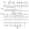
이하에서는 도 6 내지 도 8을 참조하여 본 발명의 일 실시예에 다른 표시 장치를 설명한다. 도 6은 본 발명의 일 실시예에 따른 표시 장치의 평면도이고, 도 7은 도 6의 VII-VII선을 따라 자른 단면도이고, 도 8은 도 6의 VIII-VIII선을 따라 자른 단면도이다.Hereinafter, a display device according to an exemplary embodiment of the present invention will be described with reference to FIGS. 6 to 8 . 6 is a plan view of a display device according to an exemplary embodiment, FIG. 7 is a cross-sectional view taken along line VII-VII of FIG. 6, and FIG. 8 is a cross-sectional view taken along line VIII-VIII of FIG. 6 .
도 6 내지 도 8을 참조하면, 기판(110) 위에 산화규소 또는 질화규소 등으로 만들어진 차단층(blocking layer)(111)이 위치한다.6 to 8 , a
차단층(111) 위에 복수 쌍의 제1 및 제2 반도체층(151a, 151b)이 위치한다. 제1 및 제2 반도체층(151a, 151b) 각각은 n형 또는 p형의 도전성 불순물을 포함하는 복수의 불순물 영역(extrinsic region)과 도전성 불순물을 거의 포함하지 않은 적어도 하나의 진성 영역(intrinsic region)을 포함한다.A plurality of pairs of first and
제1 반도체층(151a)에서 불순물 영역은 제1 소스 영역(153a), 제1 드레인 영역(155a) 및 중간 영역(intermediate region)(1535)을 포함한다. 제1 소스 영역(153a), 제1 드레인 영역(155a) 및 중간 영역(intermediate region)(1535) 은 n형 불순물로 도핑되어 있고 서로 분리되어 있다. 진성 영역은 불순물 영역(153a, 1535, 155a) 사이에 위치한 한 쌍의 제1 채널 영역(channel region)(154a1, 154a2) 등을 포함한다.In the
제2 반도체층(151b)에서 불순물 영역은 제2 소스 영역(153b) 및 제2 드레인 영역(155b)을 포함한다. 제2 소스 영역(153b) 및 제2 드레인 영역(155b)은 p형 불순물로 도핑되어 있고 서로 분리되어 있다. 진성 영역은 제2 소스 영역(153b) 및 제2 드레인 영역(155b) 사이에 위치한 제2 채널 영역(154b)과 제2 소스 영역(153b) 및 제2 드레인 영역(155b)으로부터 위로 길게 뻗어 나온 유지 영역(storage region)(157)을 포함한다.In the
전술한 바와 달리 제1 반도체층(151a)의 불순물 영역(153a, 155a)이 p형 불순물로 도핑되거나, 제2 반도체층(151b)의 불순물 영역(153b, 155b)이 n형 불순물로 도핑될 수 있다. 게이트 절연막(140)은 제1 반도체층(151a), 제2 반도체층(151b) 및 차단층(111) 위에 위치하며 산화규소 또는 질화규소 등으로 이루어질 수 있다.Unlike the above, the
제1 제어 전극(control electrode)(124a)을 포함하는 게이트선(gate line)(121) 및과 제2 제어 전극(124b)을 포함하는 게이트 도전체(gate conductor)가 게이트 절연막(140) 위에 위치한다.A
게이트선(121)은 게이트 신호를 전달하며 주로 가로 방향으로 뻗어 있다. 제1 제어 전극(124a)은 게이트선(121)으로부터 위로 뻗어 제1 반도체층(151a)와 교차하는데, 제1 채널 영역(154a1, 154a2)과 중첩한다.The
제2 제어 전극(124b)은 게이트선(121)과 분리되어 있고 제2 반도체층(151b)의 제2 채널 영역(154b)과 중첩한다. 제2 제어 전극(124b)은 연장되어 유지 전극(storage electrode)(127)을 이루며, 유지 전극(127)은 제2 반도체층(151b)의 유지 영역(157)과 중첩한다.The
층간 절연막(interlayer insulating film)(160)은 게이트 도전체 및 게이트 절연막(140) 위에 위치한다.An interlayer insulating
층간 절연막(160)은 제2 제어 전극(124b)을 노출하는 접촉 구멍(contact hole)(164)을 포함한다. 또한, 층간 절연막(160)과 게이트 절연막(140)은 소스 영역 및 드레인 영역(153a, 153b, 155a, 155b)을 드러내는 접촉 구멍(163a, 163b, 165a, 165b)을 포함한다.The interlayer insulating
데이터선(data line)(171), 구동 전압선(driving voltage line)(172) 및 제1 및 제2 출력 전극(output electrode)(175a, 175b)을 포함하는 데이터 도전체(data conductor)는 층간 절연막(160) 위에 위치한다.A data conductor including a
데이터선(171)은 데이터 신호를 전달하며 주로 세로 방향으로 뻗어 게이트선(121)과 교차한다. 각 데이터선(171)은 접촉 구멍(163a)을 통하여 제1 소스 영역(153a)과 연결되어 있는 제1 입력 전극(input electrode)(173a)을 포함한다.The
구동 전압선(172)은 구동 전압을 전달하며 주로 세로 방향으로 뻗어 게이트선(121)과 교차한다. 각 구동 전압선(172)은 접촉 구멍(163b)을 통하여 제2 소스 영역(153b)과 연결되어 있는 제2 입력 전극(173b)을 포함한다. 구동 전압선(172)은 유지 전극(127)과 중첩하며, 서로 연결될 수 있다.The driving
제1 출력 전극(175a)은 데이터선(171) 및 구동 전압선(172)으로부터 분리되어 있다. 제1 출력 전극(175a)은 접촉 구멍(165a)을 통하여 제1 드레인 영역(155a)에 연결되어 있고, 접촉 구멍(164)을 통하여 제2 제어 전극(124b)과 연결되어 있다.The
제2 출력 전극(175b)은 데이터선(171), 구동 전압선(172) 및 제1 출력 전극(175a)으로부터 분리되어 있으며, 접촉 구멍(165b)을 통하여 제2 드레인 영역(155b)에 연결되어 있다.The
보호막(passivation layer)(180)은 데이터 도전체(171, 172, 175a, 175b) 및 층간 절연막(160) 위에 위치하며, 보호막(180)은 제2 출력 전극(175b)을 드러내는 접촉 구멍(185)을 포함한다.A
화소 전극(pixel electrode)(190)은 보호막(180) 위에 위치한다. 화소 전극(190)은 접촉 구멍(185)을 통하여 제2 출력 전극(175b)과 물리적·전기적으로 연결되어 있다. 격벽(partition)(361)은 보호막(180) 위에 위치한다. 격벽(361)은 화소 전극(190) 가장자리 주변을 둑(bank)처럼 둘러싸서 개구부(opening)를 정의할 수 있다. 화소 전극(190) 위에는 발광 소자층(370)이 위치하고, 발광 소자층(370) 위에 공통 전극(270)이 위치한다. 발광 소자는 화소 전극(190), 발광 소자층(370) 및 공통 전극(270)을 포함한다.The
이때, 화소 전극(190)은 정공 주입 전극인 애노드, 전술한 제1 전극에 대응하며, 공통 전극(270)은 전자 주입 전극인 캐소드, 전술한 제2 전극에 대응할 수 있다. 그러나 본 발명에 따른 일 실시예는 반드시 이에 한정되는 것은 아니며, 표시 장치의 구동 방법에 따라 화소 전극(190)이 캐소드가 되고, 공통 전극(270)이 애노드가 될 수도 있다.In this case, the
발광 소자층(370)은 전술한 도 1 내지 도 5를 참조하여 설명한 혼합층(30)을 포함할 수 있으며, 이에 대한 설명을 생략한다.The light emitting
공통 전극(common electrode)(270)은 발광 소자층(370) 위에 위치한다. 공통 전극(270)은 공통 전압을 인가 받는다. 상기 설명한 표시 장치의 구조는 예시적인 것으로, 본 발명의 일 실시예에 따른 발광 소자는 다른 구조를 갖는 표시 장치에 적용될 수 있음 또한 자명하다.A
전술한 유기 발광 표시 장치에서, 제1 반도체층(151a), 게이트선(121)에 연결되어 있는 제1 제어 전극(124a), 데이터선(171)에 연결되어 있는 제1 입력 전극(173a) 및 제1 출력 전극(175a)은 스위칭 트랜지스터(switching TFT)(Qs)를 이루며, 스위칭 트랜지스터(Qs)의 채널(channel)은 제1 반도체층 (151a)의 채널 영역(154a1, 154a2)에 형성된다. 제2 반도체층 (151b), 제1 출력 전극(175a)에 연결되어 있는 제2 제어 전극(124b), 구동 전압선(172)에 연결되어 있는 제2 입력 전극(173b) 및 화소 전극(190)에 연결되어 있는 제2 출력 전극(175b)은 구동 트랜지스터(driving TFT)(Qd)를 이루며, 구동 트랜지스터(Qd)의 채널은 제2 반도체층 (151b)의 채널 영역(154b)에 형성된다. 화소 전극(190), 발광 소자층(370) 및 공통 전극(270)은 유기 발광 다이오드를 이루며, 화소 전극(190)이 애노드(anode), 공통 전극(270)이 캐소드(cathode)가 되거나 반대로 화소 전극(190)이 캐소드, 공통 전극(270)이 애노드가 된다. 서로 중첩하는 유지 전극(127)과 구동 전압선(172) 및 유지 영역(157)은 유지 축전기(storage capacitor)(Cst)를 이룬다.In the organic light emitting diode display described above, the
이상에서 본 발명의 바람직한 실시예에 대하여 상세하게 설명하였지만 본 발명의 권리범위는 이에 한정되는 것은 아니고 다음의 청구범위에서 정의하고 있는 본 발명의 기본 개념을 이용한 당업자의 여러 변형 및 개량 형태 또한 본 발명의 권리범위에 속하는 것이다.Although the preferred embodiment of the present invention has been described in detail above, the scope of the present invention is not limited thereto, and various modifications and improvements by those skilled in the art using the basic concept of the present invention as defined in the following claims are also provided. is within the scope of the
10 : 제1 전극
30 : 혼합층
31 : 양자점
33 : 정공 수송 물질
35 : 전자 수송 물질
50 : 제2 전극10: first electrode
30: mixed layer
31: quantum dot
33: hole transport material
35: electron transport material
50: second electrode
Claims (19)
Translated fromKorean제1 전극과 대향하는 제2 전극, 및
상기 제1 전극 및 상기 제2 전극 사이에 위치하는 혼합층을 포함하고,
상기 혼합층은 양자점, 정공 수송 물질, 및 전자 수송 물질을 포함하는 혼합물을 포함하며,
상기 정공 수송 물질 및 상기 전자 수송 물질의 일부는 서로 직접 접촉하는 발광 소자.a first electrode;
a second electrode opposite the first electrode, and
A mixed layer positioned between the first electrode and the second electrode,
The mixed layer includes a mixture comprising quantum dots, a hole transport material, and an electron transport material,
The hole transport material and a portion of the electron transport material are in direct contact with each other.
상기 혼합층은 복수의 단위체를 포함하고,
상기 복수의 단위체 중 적어도 하나의 단위체는 양자점, 상기 양자점을 감싸는 상기 정공 수송 물질 및 상기 전자 수송 물질 중 적어도 하나를 포함하는 발광 소자.In claim 1,
The mixed layer includes a plurality of units,
At least one unit of the plurality of units includes a quantum dot, the light emitting device including at least one of the hole transport material surrounding the quantum dot, and the electron transport material.
상기 양자점을 둘러싸는 상기 정공 수송 물질과 상기 전자 수송 물질은 교번하여 위치하는 발광 소자.in paragraph 2
A light emitting device in which the hole transport material and the electron transport material surrounding the quantum dot are alternately positioned.
상기 복수의 단위체 중 적어도 하나의 단위체는 복수의 양자점을 포함하는 발광 소자.In claim 2,
At least one of the plurality of units includes a plurality of quantum dots.
상기 양자점은 상기 제1 전극의 일면과 평행한 방향을 따라 위치하는 발광 소자.In claim 1,
The quantum dots are light emitting devices positioned along a direction parallel to one surface of the first electrode.
상기 정공 수송 물질은 유기물 및 무기물 중 적어도 하나를 포함하는 발광 소자.In claim 1,
The hole transport material is a light emitting device including at least one of an organic material and an inorganic material.
상기 정공 수송 물질은 CuO, CuO2, NiO, CuI 및 ZnTe를 포함하는 p형 산화물 반도체, 텔루르화물(telluride) 및 할로겐화물(halide) 중에서 선택된 1 이상을 포함하는 발광 소자.In claim 6,
The hole transport material is CuO, CuO2 , NiO, a light emitting device including at least one selected from a p-type oxide semiconductor including CuI and ZnTe, telluride (telluride) and halide (halide).
상기 정공 수송 물질은 PEDOT:PSS, 폴리페리나프탈렌(PPN), 폴리-p-페닐렌(PpP), 폴리티오펜(PT), C60, 바소큐프로인(BCP), 바소펜안트롤린(Bphen), 폴리(3-헥실티오펜) (P3HT) 및 OMeTAD로 이루어진 군에서 선택된 1 이상을 포함하는 발광 소자.In claim 6,
The hole transport material is PEDOT: PSS, polyperinaphthalene (PPN), poly-p-phenylene (PpP), polythiophene (PT), C60 , vasocubroin (BCP), vasophenanthroline (Bphen) ), a light emitting device comprising at least one selected from the group consisting of poly(3-hexylthiophene) (P3HT) and OMeTAD.
상기 전자 수송 물질은 무기물을 포함하는 발광 소자.In claim 1,
The electron transport material is a light emitting device including an inorganic material.
상기 전자 수송 물질은 ZnO, TiO2 및 FeF2 를 포함하는 n형 산화물 반도체 및 할로겐화물 중에서 선택된 1 이상을 포함하는 발광 소자.In claim 9,
The electron transport material is a light emitting device comprising at least one selected from n-type oxide semiconductor and halide including ZnO, TiO2 and FeF2 .
상기 정공 수송 물질 및 상기 전자 수송 물질 각각은 상기 양자점과 접촉하는 면적이 실질적으로 동일한 발광 소자.In claim 1,
Each of the hole transport material and the electron transport material has substantially the same contact area with the quantum dots.
상기 제1 전극 및 상기 혼합층 사이에 위치하는 정공 수송층, 및
상기 혼합층 및 상기 제2 전극 사이에 위치하는 전자 수송층을 더 포함하는 발광 소자.In claim 1,
a hole transport layer positioned between the first electrode and the mixed layer, and
The light emitting device further comprising an electron transport layer positioned between the mixed layer and the second electrode.
상기 기판 위에 위치하는 트랜지스터, 및
상기 트랜지스터와 연결되는 발광 소자를 포함하고,
상기 발광 소자는
제1 전극,
제1 전극과 대향하는 제2 전극, 및
상기 제1 전극 및 상기 제2 전극 사이에 위치하는 혼합층을 포함하고,
상기 혼합층은 양자점, 정공 수송 물질, 및 전자 수송 물질을 포함하는 혼합물을 포함하며,
상기 정공 수송 물질 및 상기 전자 수송 물질의 일부는 서로 직접 접촉하는표시 장치.Board,
a transistor positioned over the substrate; and
It includes a light emitting device connected to the transistor,
The light emitting device is
a first electrode;
a second electrode opposite the first electrode, and
A mixed layer positioned between the first electrode and the second electrode,
The mixed layer includes a mixture comprising quantum dots, a hole transport material, and an electron transport material,
The hole transport material and a portion of the electron transport material are in direct contact with each other.
상기 혼합층은 복수의 단위체를 포함하고,
상기 복수의 단위체 중 적어도 하나의 단위체는 양자점, 상기 양자점을 감싸는 상기 정공 수송 물질 및 상기 전자 수송 물질 중 적어도 하나를 포함하는 표시 장치.In claim 13,
The mixed layer includes a plurality of units,
At least one unit of the plurality of units includes at least one of a quantum dot, the hole transport material surrounding the quantum dot, and the electron transport material.
상기 양자점을 둘러싸는 상기 정공 수송 물질과 상기 전자 수송 물질은 교번하여 위치하는 표시 장치.in paragraph 14
The hole transport material and the electron transport material surrounding the quantum dot are alternately positioned.
상기 복수의 단위체 중 적어도 하나의 단위체는 복수의 양자점을 포함하는 표시 장치.15. In claim 14,
At least one of the plurality of units includes a plurality of quantum dots.
상기 양자점은 상기 제1 전극의 일면과 평행한 방향을 따라 위치하는 표시 장치.In claim 13,
The quantum dots are positioned along a direction parallel to one surface of the first electrode.
상기 정공 수송 물질 및 상기 전자 수송 물질 각각은 상기 양자점과 접촉하는 면적이 실질적으로 동일한 표시 장치.In claim 13,
Each of the hole transport material and the electron transport material has substantially the same contact area with the quantum dot.
상기 제1 전극 및 상기 혼합층 사이에 위치하는 정공 수송층, 및
상기 혼합층 및 상기 제2 전극 사이에 위치하는 전자 수송층을 더 포함하는 표시 장치.In claim 13,
a hole transport layer positioned between the first electrode and the mixed layer, and
The display device further comprising an electron transport layer positioned between the mixed layer and the second electrode.
Priority Applications (2)
| Application Number | Priority Date | Filing Date | Title |
|---|---|---|---|
| KR1020150185900AKR102447309B1 (en) | 2015-12-24 | 2015-12-24 | Light emitting device and display device including same |
| US15/190,267US9761822B2 (en) | 2015-12-24 | 2016-06-23 | Light emitting diode and display device including the same |
Applications Claiming Priority (1)
| Application Number | Priority Date | Filing Date | Title |
|---|---|---|---|
| KR1020150185900AKR102447309B1 (en) | 2015-12-24 | 2015-12-24 | Light emitting device and display device including same |
Publications (2)
| Publication Number | Publication Date |
|---|---|
| KR20170076860A KR20170076860A (en) | 2017-07-05 |
| KR102447309B1true KR102447309B1 (en) | 2022-09-26 |
Family
ID=59088452
Family Applications (1)
| Application Number | Title | Priority Date | Filing Date |
|---|---|---|---|
| KR1020150185900AActiveKR102447309B1 (en) | 2015-12-24 | 2015-12-24 | Light emitting device and display device including same |
Country Status (2)
| Country | Link |
|---|---|
| US (1) | US9761822B2 (en) |
| KR (1) | KR102447309B1 (en) |
Families Citing this family (13)
| Publication number | Priority date | Publication date | Assignee | Title |
|---|---|---|---|---|
| KR101936315B1 (en)* | 2017-01-05 | 2019-01-08 | 서울대학교산학협력단 | Organic light emitting device comprising cohost |
| JP2019033005A (en)* | 2017-08-08 | 2019-02-28 | 日本放送協会 | Light emitting element |
| US20210135137A1 (en)* | 2017-09-05 | 2021-05-06 | Sharp Kabushiki Kaisha | Light emitting device and manufacturing apparatus of light emitting device |
| US11217763B2 (en)* | 2017-09-05 | 2022-01-04 | Sharp Kabushiki Kaisha | Light-emitting device including light-emitting layer in which thermally activated delayed fluorescence bodies and quantum dots are dispersed and manufacturing apparatus of light-emitting device |
| US11121339B2 (en)* | 2018-05-11 | 2021-09-14 | Nanosys, Inc. | Quantum dot LED design based on resonant energy transfer |
| US11532789B2 (en) | 2018-05-29 | 2022-12-20 | Samsung Electronics Co., Ltd. | Organic thin film including semiconducting polymer and elastomer configured to be dynamic intermolecular bonded with a metal-coordination bond and organic sensor and electronic device including the same |
| KR102750348B1 (en) | 2018-11-21 | 2025-01-03 | 삼성전자주식회사 | Electroluminescent device, and display device comprising thereof |
| US10826011B1 (en)* | 2019-07-23 | 2020-11-03 | Sharp Kabushiki Kaisha | QLED fabricated by patterning with phase separated emissive layer |
| EP4014255A4 (en)* | 2019-08-16 | 2023-07-19 | Ubiquitous Energy, Inc. | PARA-PHENYLENE AS BUFFER AND COLOR ADJUSTMENT LAYERS FOR SOLAR CELLS |
| CN113258009B (en)* | 2020-04-17 | 2022-08-05 | 广东聚华印刷显示技术有限公司 | Composite material and preparation method thereof, and quantum dot light-emitting diode |
| KR102860316B1 (en)* | 2020-11-10 | 2025-09-16 | 삼성디스플레이 주식회사 | Light emitting device and electronic apparatus including the same |
| CN114512617A (en)* | 2020-11-17 | 2022-05-17 | 京东方科技集团股份有限公司 | Light-emitting device, display device and manufacturing method of light-emitting device |
| WO2022185445A1 (en)* | 2021-03-03 | 2022-09-09 | シャープ株式会社 | Light-emitting element, light-emitting device, light-emitting device production method, and electronic device |
Family Cites Families (11)
| Publication number | Priority date | Publication date | Assignee | Title |
|---|---|---|---|---|
| US6501091B1 (en)* | 1998-04-01 | 2002-12-31 | Massachusetts Institute Of Technology | Quantum dot white and colored light emitting diodes |
| CN1894799A (en)* | 2003-09-05 | 2007-01-10 | 点度量技术有限公司 | Quantum dot optoelectronic devices with nanoscale epitaxial lateral overgrowth and methods of manufacture |
| US20090039764A1 (en)* | 2005-03-17 | 2009-02-12 | Cho Kyung Sang | Quantum Dot Light-Emitting Diode Comprising Inorganic Electron Transport Layer |
| KR101109195B1 (en)* | 2005-12-19 | 2012-01-30 | 삼성전자주식회사 | 3D structure light emitting device and manufacturing method thereof |
| KR20080069085A (en)* | 2007-01-22 | 2008-07-25 | 삼성전자주식회사 | Tandem nano-dot light emitting diodes and method of manufacturing the same |
| KR20110008206A (en)* | 2008-04-03 | 2011-01-26 | 큐디 비젼, 인크. | Light Emitting Device Including Quantum Dots |
| KR101462652B1 (en) | 2008-04-23 | 2014-11-17 | 삼성전자 주식회사 | Preparation Method of Quantum Dot-Inorganic Matrix Composites |
| KR101274068B1 (en) | 2010-05-25 | 2013-06-12 | 서울대학교산학협력단 | Quantum Dot Light Emitting Diode Device and Display Using the Same |
| KR20120131945A (en) | 2011-05-27 | 2012-12-05 | 엘지디스플레이 주식회사 | Quantum dot |
| US9508949B2 (en) | 2012-07-18 | 2016-11-29 | Lg Display Co., Ltd. | Organic light-emitting device |
| KR102228142B1 (en) | 2013-04-05 | 2021-03-22 | 삼성디스플레이 주식회사 | Quantum dots, methods of manufacturing quantum dots and methods of manufacturing organic light emitting devices using the same |
- 2015
- 2015-12-24KRKR1020150185900Apatent/KR102447309B1/enactiveActive
- 2016
- 2016-06-23USUS15/190,267patent/US9761822B2/enactiveActive
Also Published As
| Publication number | Publication date |
|---|---|
| KR20170076860A (en) | 2017-07-05 |
| US20170186988A1 (en) | 2017-06-29 |
| US9761822B2 (en) | 2017-09-12 |
Similar Documents
| Publication | Publication Date | Title |
|---|---|---|
| KR102447309B1 (en) | Light emitting device and display device including same | |
| US11818907B2 (en) | Quantum-dot light emitting device comprising solution processed charge generation junction and manufacturing method thereof | |
| US9905790B2 (en) | Optoelectronic device including quantum dot | |
| US11871621B2 (en) | Display device comprising partition walls | |
| US11018311B2 (en) | Device with quantum dot emissive layer and display device comprising the same | |
| KR102110780B1 (en) | Quantum dot light emitting device and the method for manufacturing thereof | |
| KR102001734B1 (en) | Quantum dot lightemitting device and manufacturing method therefor | |
| US20220310963A1 (en) | Thin-film light-emitting device including charge generating junction layer and method of fabricating thin-film light-emitting device | |
| KR102766478B1 (en) | Display apparatus and manufacturing the same | |
| US20180175132A1 (en) | Organic light emitting diode and organic light emitting display device including the same | |
| JP2021086151A (en) | Display panel and display device | |
| KR20140025161A (en) | Method of manufacturing quantum dot device, quantom dot device using the same, and method of measuring electron mobility of quantum dot device | |
| KR102655061B1 (en) | Manufacturing method for quantum dot layer and manufacturing method for luminescence device including the quantum dot layer and display device including the quantum dot layer | |
| KR102097587B1 (en) | Quantum dot light emitting device and manufacturing method for thereof | |
| US20230232649A1 (en) | Display device | |
| US20230023840A1 (en) | Quantum dot film, method for preparing the same, and quantum dot light emitting diode | |
| KR102575029B1 (en) | Display device | |
| US20250107314A1 (en) | Display device and method for manufacturing the same | |
| KR20170091818A (en) | Light emitting diode | |
| US20230209961A1 (en) | Light emitting display device | |
| KR20200064876A (en) | Display device and manufacturing method thereof | |
| KR20240178270A (en) | Display device | |
| CN118284089A (en) | Quantum dot light-emitting device, preparation method thereof and display device | |
| CN117794306A (en) | Light-emitting device, preparation method thereof and display device | |
| CN118695641A (en) | A light emitting device, a manufacturing method thereof and a display device |
Legal Events
| Date | Code | Title | Description |
|---|---|---|---|
| PA0109 | Patent application | St.27 status event code:A-0-1-A10-A12-nap-PA0109 | |
| PG1501 | Laying open of application | St.27 status event code:A-1-1-Q10-Q12-nap-PG1501 | |
| P22-X000 | Classification modified | St.27 status event code:A-2-2-P10-P22-nap-X000 | |
| R18-X000 | Changes to party contact information recorded | St.27 status event code:A-3-3-R10-R18-oth-X000 | |
| PA0201 | Request for examination | St.27 status event code:A-1-2-D10-D11-exm-PA0201 | |
| E902 | Notification of reason for refusal | ||
| PE0902 | Notice of grounds for rejection | St.27 status event code:A-1-2-D10-D21-exm-PE0902 | |
| P11-X000 | Amendment of application requested | St.27 status event code:A-2-2-P10-P11-nap-X000 | |
| P13-X000 | Application amended | St.27 status event code:A-2-2-P10-P13-nap-X000 | |
| E701 | Decision to grant or registration of patent right | ||
| PE0701 | Decision of registration | St.27 status event code:A-1-2-D10-D22-exm-PE0701 | |
| GRNT | Written decision to grant | ||
| PR0701 | Registration of establishment | St.27 status event code:A-2-4-F10-F11-exm-PR0701 | |
| PR1002 | Payment of registration fee | St.27 status event code:A-2-2-U10-U11-oth-PR1002 Fee payment year number:1 | |
| PG1601 | Publication of registration | St.27 status event code:A-4-4-Q10-Q13-nap-PG1601 | |
| P22-X000 | Classification modified | St.27 status event code:A-4-4-P10-P22-nap-X000 | |
| P22-X000 | Classification modified | St.27 status event code:A-4-4-P10-P22-nap-X000 | |
| P22-X000 | Classification modified | St.27 status event code:A-4-4-P10-P22-nap-X000 | |
| P22-X000 | Classification modified | St.27 status event code:A-4-4-P10-P22-nap-X000 |