KR102447308B1 - organic light emitting diode display - Google Patents
organic light emitting diode displayDownload PDFInfo
- Publication number
- KR102447308B1 KR102447308B1KR1020150074879AKR20150074879AKR102447308B1KR 102447308 B1KR102447308 B1KR 102447308B1KR 1020150074879 AKR1020150074879 AKR 1020150074879AKR 20150074879 AKR20150074879 AKR 20150074879AKR 102447308 B1KR102447308 B1KR 102447308B1
- Authority
- KR
- South Korea
- Prior art keywords
- layer
- light emitting
- electrode
- intermediate layer
- metal
- Prior art date
- Legal status (The legal status is an assumption and is not a legal conclusion. Google has not performed a legal analysis and makes no representation as to the accuracy of the status listed.)
- Active
Links
- 239000000463materialSubstances0.000claimsabstractdescription79
- 238000002347injectionMethods0.000claimsabstractdescription72
- 239000007924injectionSubstances0.000claimsabstractdescription72
- 229910052751metalInorganic materials0.000claimsabstractdescription34
- 239000002184metalSubstances0.000claimsabstractdescription34
- 239000000758substrateSubstances0.000claimsabstractdescription23
- 239000010409thin filmSubstances0.000claimsabstractdescription23
- 229910052747lanthanoidInorganic materials0.000claimsabstractdescription18
- 229910052736halogenInorganic materials0.000claimsabstractdescription17
- 150000002367halogensChemical class0.000claimsabstractdescription17
- 150000002602lanthanoidsChemical class0.000claimsabstractdescription15
- 229910052723transition metalInorganic materials0.000claimsabstractdescription14
- 150000003624transition metalsChemical class0.000claimsabstractdescription14
- 229910052741iridiumInorganic materials0.000claimsdescription6
- -1lanthanide metalsChemical class0.000claimsdescription6
- 229910052755nonmetalInorganic materials0.000claimsdescription6
- 229910010193LiAgInorganic materials0.000claimsdescription5
- 229910011687LiCuInorganic materials0.000claimsdescription5
- 229910052790berylliumInorganic materials0.000claimsdescription5
- 150000001875compoundsChemical class0.000claimsdescription5
- 229910052709silverInorganic materials0.000claimsdescription5
- 229910052796boronInorganic materials0.000claimsdescription4
- 150000002739metalsChemical class0.000claimsdescription4
- 229910052799carbonInorganic materials0.000claimsdescription3
- 229910052804chromiumInorganic materials0.000claimsdescription3
- 229910052802copperInorganic materials0.000claimsdescription3
- 229910052737goldInorganic materials0.000claimsdescription3
- 229910052742ironInorganic materials0.000claimsdescription3
- 229910052753mercuryInorganic materials0.000claimsdescription3
- 229910052750molybdenumInorganic materials0.000claimsdescription3
- 229910052758niobiumInorganic materials0.000claimsdescription3
- 229910052763palladiumInorganic materials0.000claimsdescription3
- 229910052697platinumInorganic materials0.000claimsdescription3
- 229910052702rheniumInorganic materials0.000claimsdescription3
- 229910052703rhodiumInorganic materials0.000claimsdescription3
- 229910052718tinInorganic materials0.000claimsdescription3
- 229910052719titaniumInorganic materials0.000claimsdescription3
- 229910052720vanadiumInorganic materials0.000claimsdescription3
- 229910052721tungstenInorganic materials0.000claimsdescription2
- 229910052725zincInorganic materials0.000claimsdescription2
- 239000010410layerSubstances0.000description205
- 230000005525hole transportEffects0.000description13
- 238000005538encapsulationMethods0.000description8
- 239000004065semiconductorSubstances0.000description8
- 239000000872bufferSubstances0.000description7
- 239000011229interlayerSubstances0.000description7
- 239000011777magnesiumSubstances0.000description6
- 229920005989resinPolymers0.000description6
- 239000011347resinSubstances0.000description6
- VYPSYNLAJGMNEJ-UHFFFAOYSA-Nsilicon dioxideInorganic materialsO=[Si]=OVYPSYNLAJGMNEJ-UHFFFAOYSA-N0.000description6
- 229910052814silicon oxideInorganic materials0.000description6
- 239000002019doping agentSubstances0.000description5
- 239000010408filmSubstances0.000description5
- 239000010416ion conductorSubstances0.000description5
- 239000007983Tris bufferSubstances0.000description4
- 229910052782aluminiumInorganic materials0.000description4
- XAGFODPZIPBFFR-UHFFFAOYSA-NaluminiumChemical compound[Al]XAGFODPZIPBFFR-UHFFFAOYSA-N0.000description4
- 239000012535impuritySubstances0.000description4
- 229910052749magnesiumInorganic materials0.000description4
- OAICVXFJPJFONN-UHFFFAOYSA-NPhosphorusChemical compound[P]OAICVXFJPJFONN-UHFFFAOYSA-N0.000description3
- 239000004642PolyimideSubstances0.000description3
- 229910052581Si3N4Inorganic materials0.000description3
- 229910004205SiNXInorganic materials0.000description3
- GKOZUEZYRPOHIO-UHFFFAOYSA-Niridium atomChemical compound[Ir]GKOZUEZYRPOHIO-UHFFFAOYSA-N0.000description3
- 238000000034methodMethods0.000description3
- 239000012044organic layerSubstances0.000description3
- 229920001721polyimidePolymers0.000description3
- HQVNEWCFYHHQES-UHFFFAOYSA-Nsilicon nitrideChemical compoundN12[Si]34N5[Si]62N3[Si]51N64HQVNEWCFYHHQES-UHFFFAOYSA-N0.000description3
- POILWHVDKZOXJZ-ARJAWSKDSA-M(z)-4-oxopent-2-en-2-olateChemical compoundC\C([O-])=C\C(C)=OPOILWHVDKZOXJZ-ARJAWSKDSA-M0.000description2
- VBQVHWHWZOUENI-UHFFFAOYSA-N1-phenyl-2H-quinolineChemical compoundC1C=CC2=CC=CC=C2N1C1=CC=CC=C1VBQVHWHWZOUENI-UHFFFAOYSA-N0.000description2
- 229910052684CeriumInorganic materials0.000description2
- FYYHWMGAXLPEAU-UHFFFAOYSA-NMagnesiumChemical compound[Mg]FYYHWMGAXLPEAU-UHFFFAOYSA-N0.000description2
- 229910052779NeodymiumInorganic materials0.000description2
- 229910052777PraseodymiumInorganic materials0.000description2
- XUIMIQQOPSSXEZ-UHFFFAOYSA-NSiliconChemical compound[Si]XUIMIQQOPSSXEZ-UHFFFAOYSA-N0.000description2
- BQCADISMDOOEFD-UHFFFAOYSA-NSilverChemical compound[Ag]BQCADISMDOOEFD-UHFFFAOYSA-N0.000description2
- 229910006404SnO 2Inorganic materials0.000description2
- 229910052769YtterbiumInorganic materials0.000description2
- XLOMVQKBTHCTTD-UHFFFAOYSA-NZinc monoxideChemical compound[Zn]=OXLOMVQKBTHCTTD-UHFFFAOYSA-N0.000description2
- CUJRVFIICFDLGR-UHFFFAOYSA-NacetylacetonateChemical compoundCC(=O)[CH-]C(C)=OCUJRVFIICFDLGR-UHFFFAOYSA-N0.000description2
- 238000000231atomic layer depositionMethods0.000description2
- UMIVXZPTRXBADB-UHFFFAOYSA-NbenzocyclobuteneChemical compoundC1=CC=C2CCC2=C1UMIVXZPTRXBADB-UHFFFAOYSA-N0.000description2
- 229910052794bromiumInorganic materials0.000description2
- 229910052792caesiumInorganic materials0.000description2
- 229910052791calciumInorganic materials0.000description2
- 239000000919ceramicSubstances0.000description2
- 238000000224chemical solution depositionMethods0.000description2
- 238000005229chemical vapour depositionMethods0.000description2
- 229910052801chlorineInorganic materials0.000description2
- 239000004020conductorSubstances0.000description2
- 239000010949copperSubstances0.000description2
- 229910052731fluorineInorganic materials0.000description2
- 229910052730franciumInorganic materials0.000description2
- AMGQUBHHOARCQH-UHFFFAOYSA-Nindium;oxotinChemical compound[In].[Sn]=OAMGQUBHHOARCQH-UHFFFAOYSA-N0.000description2
- 239000011147inorganic materialSubstances0.000description2
- 229910052740iodineInorganic materials0.000description2
- UEEXRMUCXBPYOV-UHFFFAOYSA-Niridium;2-phenylpyridineChemical compound[Ir].C1=CC=CC=C1C1=CC=CC=N1.C1=CC=CC=C1C1=CC=CC=N1.C1=CC=CC=C1C1=CC=CC=N1UEEXRMUCXBPYOV-UHFFFAOYSA-N0.000description2
- 229910052746lanthanumInorganic materials0.000description2
- 239000004973liquid crystal related substanceSubstances0.000description2
- 229910052744lithiumInorganic materials0.000description2
- 239000007769metal materialSubstances0.000description2
- 239000011368organic materialSubstances0.000description2
- BASFCYQUMIYNBI-UHFFFAOYSA-NplatinumSubstances[Pt]BASFCYQUMIYNBI-UHFFFAOYSA-N0.000description2
- 229920000642polymerPolymers0.000description2
- 229910052700potassiumInorganic materials0.000description2
- 230000004044responseEffects0.000description2
- 229910052701rubidiumInorganic materials0.000description2
- 229910052710siliconInorganic materials0.000description2
- 239000010703siliconSubstances0.000description2
- 239000004332silverSubstances0.000description2
- 239000002356single layerSubstances0.000description2
- 229910052708sodiumInorganic materials0.000description2
- 238000004544sputter depositionMethods0.000description2
- 229910052712strontiumInorganic materials0.000description2
- XOLBLPGZBRYERU-UHFFFAOYSA-Ntin dioxideChemical compoundO=[Sn]=OXOLBLPGZBRYERU-UHFFFAOYSA-N0.000description2
- 229910001887tin oxideInorganic materials0.000description2
- TVIVIEFSHFOWTE-UHFFFAOYSA-Ktri(quinolin-8-yloxy)alumaneChemical compound[Al+3].C1=CN=C2C([O-])=CC=CC2=C1.C1=CN=C2C([O-])=CC=CC2=C1.C1=CN=C2C([O-])=CC=CC2=C1TVIVIEFSHFOWTE-UHFFFAOYSA-K0.000description2
- 239000011701zincSubstances0.000description2
- YVTHLONGBIQYBO-UHFFFAOYSA-Nzinc indium(3+) oxygen(2-)Chemical compound[O--].[Zn++].[In+3]YVTHLONGBIQYBO-UHFFFAOYSA-N0.000description2
- ZSYMVHGRKPBJCQ-UHFFFAOYSA-N1,1'-biphenyl;9h-carbazoleChemical groupC1=CC=CC=C1C1=CC=CC=C1.C1=CC=C2C3=CC=CC=C3NC2=C1ZSYMVHGRKPBJCQ-UHFFFAOYSA-N0.000description1
- LPCWDYWZIWDTCV-UHFFFAOYSA-N1-phenylisoquinolineChemical compoundC1=CC=CC=C1C1=NC=CC2=CC=CC=C12LPCWDYWZIWDTCV-UHFFFAOYSA-N0.000description1
- VFMUXPQZKOKPOF-UHFFFAOYSA-N2,3,7,8,12,13,17,18-octaethyl-21,23-dihydroporphyrin platinumChemical compound[Pt].CCc1c(CC)c2cc3[nH]c(cc4nc(cc5[nH]c(cc1n2)c(CC)c5CC)c(CC)c4CC)c(CC)c3CCVFMUXPQZKOKPOF-UHFFFAOYSA-N0.000description1
- KXGFMDJXCMQABM-UHFFFAOYSA-N2-methoxy-6-methylphenolChemical compound[CH]OC1=CC=CC([CH])=C1OKXGFMDJXCMQABM-UHFFFAOYSA-N0.000description1
- HONWGFNQCPRRFM-UHFFFAOYSA-N2-n-(3-methylphenyl)-1-n,1-n,2-n-triphenylbenzene-1,2-diamineChemical compoundCC1=CC=CC(N(C=2C=CC=CC=2)C=2C(=CC=CC=2)N(C=2C=CC=CC=2)C=2C=CC=CC=2)=C1HONWGFNQCPRRFM-UHFFFAOYSA-N0.000description1
- OGGKVJMNFFSDEV-UHFFFAOYSA-N3-methyl-n-[4-[4-(n-(3-methylphenyl)anilino)phenyl]phenyl]-n-phenylanilineChemical compoundCC1=CC=CC(N(C=2C=CC=CC=2)C=2C=CC(=CC=2)C=2C=CC(=CC=2)N(C=2C=CC=CC=2)C=2C=C(C)C=CC=2)=C1OGGKVJMNFFSDEV-UHFFFAOYSA-N0.000description1
- 239000004925Acrylic resinSubstances0.000description1
- 229920000178Acrylic resinPolymers0.000description1
- ZOXJGFHDIHLPTG-UHFFFAOYSA-NBoronChemical compound[B]ZOXJGFHDIHLPTG-UHFFFAOYSA-N0.000description1
- YNPNZTXNASCQKK-UHFFFAOYSA-NPhenanthreneNatural productsC1=CC=C2C3=CC=CC=C3C=CC2=C1YNPNZTXNASCQKK-UHFFFAOYSA-N0.000description1
- 239000004952PolyamideSubstances0.000description1
- 239000004695Polyether sulfoneSubstances0.000description1
- 239000004734Polyphenylene sulfideSubstances0.000description1
- DGEZNRSVGBDHLK-UHFFFAOYSA-N[1,10]phenanthrolineChemical compoundC1=CN=C2C3=NC=CC=C3C=CC2=C1DGEZNRSVGBDHLK-UHFFFAOYSA-N0.000description1
- 150000001408amidesChemical class0.000description1
- UFVXQDWNSAGPHN-UHFFFAOYSA-Kbis[(2-methylquinolin-8-yl)oxy]-(4-phenylphenoxy)alumaneChemical compound[Al+3].C1=CC=C([O-])C2=NC(C)=CC=C21.C1=CC=C([O-])C2=NC(C)=CC=C21.C1=CC([O-])=CC=C1C1=CC=CC=C1UFVXQDWNSAGPHN-UHFFFAOYSA-K0.000description1
- 230000000903blocking effectEffects0.000description1
- 125000004556carbazol-9-yl groupChemical groupC1=CC=CC=2C3=CC=CC=C3N(C12)*0.000description1
- AVWLPUQJODERGA-UHFFFAOYSA-Lcobalt(2+);diiodideChemical compound[Co+2].[I-].[I-]AVWLPUQJODERGA-UHFFFAOYSA-L0.000description1
- XCJYREBRNVKWGJ-UHFFFAOYSA-Ncopper(II) phthalocyanineChemical compound[Cu+2].C12=CC=CC=C2C(N=C2[N-]C(C3=CC=CC=C32)=N2)=NC1=NC([C]1C=CC=CC1=1)=NC=1N=C1[C]3C=CC=CC3=C2[N-]1XCJYREBRNVKWGJ-UHFFFAOYSA-N0.000description1
- LSXDOTMGLUJQCM-UHFFFAOYSA-Mcopper(i) iodideChemical compoundI[Cu]LSXDOTMGLUJQCM-UHFFFAOYSA-M0.000description1
- 230000000694effectsEffects0.000description1
- 239000003822epoxy resinSubstances0.000description1
- 239000011521glassSubstances0.000description1
- RBTKNAXYKSUFRK-UHFFFAOYSA-Nheliogen blueChemical compound[Cu].[N-]1C2=C(C=CC=C3)C3=C1N=C([N-]1)C3=CC=CC=C3C1=NC([N-]1)=C(C=CC=C3)C3=C1N=C([N-]1)C3=CC=CC=C3C1=N2RBTKNAXYKSUFRK-UHFFFAOYSA-N0.000description1
- 229910010272inorganic materialInorganic materials0.000description1
- 238000004020luminiscence typeMethods0.000description1
- 238000012986modificationMethods0.000description1
- 230000004048modificationEffects0.000description1
- 150000002843nonmetalsChemical class0.000description1
- 230000035515penetrationEffects0.000description1
- 125000002080perylenyl groupChemical groupC1(=CC=C2C=CC=C3C4=CC=CC5=CC=CC(C1=C23)=C45)*0.000description1
- CSHWQDPOILHKBI-UHFFFAOYSA-NperyreneNatural productsC1=CC(C2=CC=CC=3C2=C2C=CC=3)=C3C2=CC=CC3=C1CSHWQDPOILHKBI-UHFFFAOYSA-N0.000description1
- 229920001568phenolic resinPolymers0.000description1
- 239000005011phenolic resinSubstances0.000description1
- 239000004033plasticSubstances0.000description1
- 229920003023plasticPolymers0.000description1
- 229920003207poly(ethylene-2,6-naphthalate)Polymers0.000description1
- 229920003229poly(methyl methacrylate)Polymers0.000description1
- 229920000058polyacrylatePolymers0.000description1
- 229920002647polyamidePolymers0.000description1
- 229920000515polycarbonatePolymers0.000description1
- 239000004417polycarbonateSubstances0.000description1
- 229910021420polycrystalline siliconInorganic materials0.000description1
- 229920000647polyepoxidePolymers0.000description1
- 229920006393polyether sulfonePolymers0.000description1
- 239000011112polyethylene naphthalateSubstances0.000description1
- 229920000139polyethylene terephthalatePolymers0.000description1
- 239000005020polyethylene terephthalateSubstances0.000description1
- 239000004926polymethyl methacrylateSubstances0.000description1
- 229920000069polyphenylene sulfidePolymers0.000description1
- 229920005591polysiliconPolymers0.000description1
- 230000008569processEffects0.000description1
- 239000010453quartzSubstances0.000description1
- 239000000377silicon dioxideSubstances0.000description1
- 229910001220stainless steelInorganic materials0.000description1
- 239000010935stainless steelSubstances0.000description1
- 238000002207thermal evaporationMethods0.000description1
- 229920006305unsaturated polyesterPolymers0.000description1
- 229920006337unsaturated polyester resinPolymers0.000description1
- 239000013585weight reducing agentSubstances0.000description1
Images

Classifications
- H01L27/3258—
- H—ELECTRICITY
- H10—SEMICONDUCTOR DEVICES; ELECTRIC SOLID-STATE DEVICES NOT OTHERWISE PROVIDED FOR
- H10K—ORGANIC ELECTRIC SOLID-STATE DEVICES
- H10K50/00—Organic light-emitting devices
- H10K50/10—OLEDs or polymer light-emitting diodes [PLED]
- H10K50/17—Carrier injection layers
- H10K50/171—Electron injection layers
- H01L27/3262—
- H01L51/5008—
- H01L51/5088—
- H01L51/5092—
- H—ELECTRICITY
- H10—SEMICONDUCTOR DEVICES; ELECTRIC SOLID-STATE DEVICES NOT OTHERWISE PROVIDED FOR
- H10K—ORGANIC ELECTRIC SOLID-STATE DEVICES
- H10K50/00—Organic light-emitting devices
- H10K50/10—OLEDs or polymer light-emitting diodes [PLED]
- H10K50/14—Carrier transporting layers
- H10K50/16—Electron transporting layers
- H—ELECTRICITY
- H10—SEMICONDUCTOR DEVICES; ELECTRIC SOLID-STATE DEVICES NOT OTHERWISE PROVIDED FOR
- H10K—ORGANIC ELECTRIC SOLID-STATE DEVICES
- H10K50/00—Organic light-emitting devices
- H10K50/10—OLEDs or polymer light-emitting diodes [PLED]
- H10K50/17—Carrier injection layers
- H—ELECTRICITY
- H10—SEMICONDUCTOR DEVICES; ELECTRIC SOLID-STATE DEVICES NOT OTHERWISE PROVIDED FOR
- H10K—ORGANIC ELECTRIC SOLID-STATE DEVICES
- H10K50/00—Organic light-emitting devices
- H10K50/80—Constructional details
- H10K50/805—Electrodes
- H10K50/82—Cathodes
- H10K50/824—Cathodes combined with auxiliary electrodes
- H—ELECTRICITY
- H10—SEMICONDUCTOR DEVICES; ELECTRIC SOLID-STATE DEVICES NOT OTHERWISE PROVIDED FOR
- H10K—ORGANIC ELECTRIC SOLID-STATE DEVICES
- H10K59/00—Integrated devices, or assemblies of multiple devices, comprising at least one organic light-emitting element covered by group H10K50/00
- H10K59/10—OLED displays
- H10K59/12—Active-matrix OLED [AMOLED] displays
- H10K59/123—Connection of the pixel electrodes to the thin film transistors [TFT]
- H01L2227/32—
- H—ELECTRICITY
- H10—SEMICONDUCTOR DEVICES; ELECTRIC SOLID-STATE DEVICES NOT OTHERWISE PROVIDED FOR
- H10K—ORGANIC ELECTRIC SOLID-STATE DEVICES
- H10K2102/00—Constructional details relating to the organic devices covered by this subclass
- H—ELECTRICITY
- H10—SEMICONDUCTOR DEVICES; ELECTRIC SOLID-STATE DEVICES NOT OTHERWISE PROVIDED FOR
- H10K—ORGANIC ELECTRIC SOLID-STATE DEVICES
- H10K2102/00—Constructional details relating to the organic devices covered by this subclass
- H10K2102/301—Details of OLEDs
- H10K2102/351—Thickness
- H—ELECTRICITY
- H10—SEMICONDUCTOR DEVICES; ELECTRIC SOLID-STATE DEVICES NOT OTHERWISE PROVIDED FOR
- H10K—ORGANIC ELECTRIC SOLID-STATE DEVICES
- H10K50/00—Organic light-emitting devices
- H10K50/80—Constructional details
- H10K50/805—Electrodes
- H10K50/81—Anodes
- H10K50/814—Anodes combined with auxiliary electrodes, e.g. ITO layer combined with metal lines
Landscapes
- Physics & Mathematics (AREA)
- Optics & Photonics (AREA)
- Engineering & Computer Science (AREA)
- Microelectronics & Electronic Packaging (AREA)
- Electroluminescent Light Sources (AREA)
- Illuminated Signs And Luminous Advertising (AREA)
- Control Of El Displays (AREA)
Abstract
Translated fromKoreanDescription
Translated fromKorean본 발명은 유기 발광 표시 장치에 관한 것이다.The present invention relates to an organic light emitting diode display.
최근 모니터 또는 텔레비전 등의 경량화 및 박형화가 요구되고 있으며, 이러한 요구에 따라 음극선관(cathode ray tube, CRT)이 액정 표시 장치(liquid crystal display, LCD)로 대체되고 있다. 그러나, 액정 표시 장치는 수발광 장치로서 별도의 백라이트(backlight)가 필요할 뿐만 아니라, 응답 속도 및 시야각 등에서 한계가 있다.Recently, weight reduction and thinning of monitors or televisions are required, and a cathode ray tube (CRT) is being replaced by a liquid crystal display (LCD) according to these demands. However, as a light-receiving device, a liquid crystal display device not only requires a separate backlight, but also has limitations in response speed and viewing angle.
최근 이러한 한계를 극복할 수 있는 표시 장치로서, 자발광형 표시소자로 시야각이 넓고 콘트라스트가 우수할 뿐만 아니라 응답시간이 빠르다는 장점을 가진 유기 발광 표시 장치(organic light emitting display device)가 커다란 주목을 받고 있다.Recently, as a display device that can overcome this limitation, an organic light emitting display device, which is a self-luminous display device, has a wide viewing angle, excellent contrast, and fast response time. are receiving
유기 발광 표시 장치는 발광을 위한 유기 발광 소자를 포함하고, 이러한 유기 발광 소자는 하나의 전극으로부터 주입된 전자(electron)와 다른 전극으로부터 주입된 정공(hole)이 발광층에서 결합하여 여기자(exciton)를 형성하고, 여기자가 에너지를 방출하면서 발광한다.An organic light emitting display device includes an organic light emitting device for light emission, and in the organic light emitting device, electrons injected from one electrode and holes injected from another electrode are combined in an emission layer to generate excitons. formed, and the exciton emits energy and emits light.
그러나 종래 유기 발광 표시 장치는 구동 전압이 높고 발광 휘도나 발광 효율이 낮으며 발광 수명이 짧은 문제점이 있었다.However, the conventional organic light emitting diode display has problems in that a driving voltage is high, luminance or luminous efficiency is low, and a luminescence lifetime is short.
본 발명이 이루고자 하는 기술적 과제는 유기 발광 소자의 전극의 계면 저항을 감소시키고 표면을 균일하게 형성할 수 있어, 발광 효율을 증가 시킬 수 있는 유기 발광 표시 장치를 제공하고자 한다.An object of the present invention is to provide an organic light emitting display device capable of reducing interfacial resistance of an electrode of an organic light emitting diode and forming a uniform surface, thereby increasing luminous efficiency.
이러한 과제를 해결하기 위하여 본 발명의 실시예에 따르면, 기판, 상기 기판 위에 형성된 박막 트랜지스터, 상기 박막 트랜지스터 위에 위치하고, 상기 박막 트랜지스터와 전기적으로 연결되어 있는 제1 전극, 상기 제1 전극 위에 위치하는 정공 주입층, 상기 정공 주입층 위에 위치하는 발광층, 상기 발광층 위에 위치하는 전자 주입층, 상기 전자 주입층 위에 위치하는 제1 중간층, 및 상기 제1 중간층 위에 위치하는 제2 전극을 포함하며, 상기 제1 중간층은 1족, 2족, 란탄계 금속 및 전이 금속 중 적어도 하나의 원소를 포함하는 제1 물질 및 할로겐을 포함하는 제2 물질로 형성된 쌍극자 물질을 포함하는 유기 발광 표시 장치를 제공한다.According to an embodiment of the present invention in order to solve this problem, a substrate, a thin film transistor formed on the substrate, a first electrode positioned on the thin film transistor and electrically connected to the thin film transistor, and a hole positioned on the first electrode An injection layer, an emission layer located on the hole injection layer, an electron injection layer located on the emission layer, a first intermediate layer located on the electron injection layer, and a second electrode located on the first intermediate layer, the first The intermediate layer provides an organic light emitting diode display including a dipole material formed of a first material including at least one of Group 1, Group 2, a lanthanide-based metal, and a transition metal, and a second material including a halogen.
상기 제1 물질은 1족, 2족, 란탄계 금속 중 하나의 원소, 및 전이 금속 중 하나의 원소를 포함할 수 있다.The first material may include one element among Group 1, Group 2, and lanthanide-based metals, and one element among transition metals.
상기 제1 중간층은 삼원계 무기 쌍극자 물질을 포함할 수 있다.The first intermediate layer may include a ternary inorganic dipole material.
상기 제1 중간층은 LiAg4I5, NaAg4I5, KAg4I5, RbAg4I5, CsAg4I5, LiCu4I5, NaCu4I5, KCu4I5, RbCu4I5 및 CsCu4I5중 선택된 적어도 하나의 화합물을 포함할 수 있다.The first intermediate layer is LiAg4 I5 , NaAg4 I5 , KAg4 I5 , RbAg4 I5 , CsAg4 I5 , LiCu4 I5 , NaCu4 I5 , KCu4 I5 , RbCu4 I5 , and CsCu4 I5It may include at least one compound selected from among.
상기 제1 중간층의 두께는 10~200Å의 범위로 형성될 수 있다.The thickness of the first intermediate layer may be formed in a range of 10 to 200 Å.
상기 전자 주입층은 금속 기반의 할로겐 쌍극자 물질을 포함할 수 있다.The electron injection layer may include a metal-based halogen dipole material.
상기 전자 주입층에 포함되는 상기 금속은 1족, 2족 또는 란탄계 금속 중 선택된 어느 하나 이상의 물질을 포함할 수 있다.The metal included in the electron injection layer may include at least one material selected from Group 1, Group 2, and/or lanthanide-based metals.
상기 정공 주입층은 금속 또는 비금속 기반의 할로겐 쌍극자 물질을 포함할 수 있다.The hole injection layer may include a metal or non-metal-based halogen dipole material.
상기 정공 주입층에 포함되는 금속 또는 비금속은 Ag, Au, B, Be, C, Co, Cr, Cu, Fe, Hg, Ir, Mo, Nb, Ni, Os, Pd, Pt, Re, Rh, Ru, Sb, Se, Si, Sn, Ta, Te, Ti, V, W 및 Zn 중 선택된 적어도 하나의 물질을 포함할 수 있다.The metal or non-metal included in the hole injection layer is Ag, Au, B, Be, C, Co, Cr, Cu, Fe, Hg, Ir, Mo, Nb, Ni, Os, Pd, Pt, Re, Rh, Ru , Sb, Se, Si, Sn, Ta, Te, Ti, V, W, and may include at least one material selected from Zn.
상기 제1 전극 및 상기 제1 층 사이에 위치하는 제2 중간층을 더 포함하며, 상기 제2 중간층은 1족, 2족, 란탄계 금속 및 전이 금속 중 적어도 하나의 원소를 포함하는 제3 물질 및 할로겐을 포함하는 제4 물질로 형성된 쌍극자 물질을 포함할 수 있다.and a second intermediate layer positioned between the first electrode and the first layer, wherein the second intermediate layer includes a third material including at least one element of Group 1, Group 2, a lanthanide metal, and a transition metal; It may include a dipole material formed of a fourth material including halogen.
상기 제3 물질은 1족, 2족, 란탄계 금속 중 하나의 원소, 및 전이 금속 중 하나의 원소를 포함할 수 있다.The third material may include one element among Group 1, Group 2, and lanthanide metals, and one element among transition metals.
상기 제1 중간층 및 상기 제2 중간층은 동일한 물질을 포함할 수 있다.The first intermediate layer and the second intermediate layer may include the same material.
또한, 본 발명의 다른 실시예에 따르면, 기판, 상기 기판 위에 형성된 박막 트랜지스터, 상기 박막 트랜지스터 위에 위치하고, 상기 박막 트랜지스터와 전기적으로 연결되어 있는 제1 전극, 상기 제1 전극 위에 위치하는 중간층, 상기 중간층 위에 위치하는 정공 주입층, 상기 정공 주입층 위에 위치하는 발광층, 상기 발광층 위에 위치하는 전자 주입층, 상기 전자 주입층 위에 위치하는 제2 전극을 포함하며, 상기 중간층은 1족, 2족, 란탄계 금속 및 전이 금속 중 적어도 하나의 원소를 포함하는 제1 물질 및 할로겐을 포함하는 제2 물질로 형성된 쌍극자 물질을 포함하는 유기 발광 표시 장치를 제공한다.In addition, according to another embodiment of the present invention, a substrate, a thin film transistor formed on the substrate, a first electrode positioned on the thin film transistor and electrically connected to the thin film transistor, an intermediate layer positioned on the first electrode, and the intermediate layer a hole injection layer positioned on the hole injection layer, a light emitting layer positioned on the hole injection layer, an electron injection layer positioned on the light emitting layer, and a second electrode positioned on the electron injection layer, wherein the intermediate layer is a group 1, group 2, or lanthanide type Provided is an organic light emitting diode display including a dipole material formed of a first material including at least one element of a metal and a transition metal and a second material including a halogen.
이상과 같이 본 발명의 실시예에 따르면, 전극과 발광층 사이에 이온 전도체 물질을 포함하는 중간층을 형성하여 전극의 계면 저항을 감소시키고 표면을 균일하게 형성할 수 있어, 유기 발광 표시 장치의 발광 효율을 증가시킬 수 있다.As described above, according to the embodiment of the present invention, an intermediate layer including an ion conductor material is formed between the electrode and the light emitting layer to reduce the interfacial resistance of the electrode and uniformly form the surface, thereby improving the luminous efficiency of the organic light emitting display device. can increase
도 1은 본 발명의 일 실시예에 따른 유기 발광 표시 장치를 나타내는 단면도이다.
도 2는 도 1에서 유기 발광 소자의 일부를 확대한 부분 단면도이다.
도 3은 본 발명의 다른 실시예에 따른 유기 발광 소자의 일부를 확대한 부분 단면도이다.
도 4는 본 발명의 또 다른 실시예에 따른 유기 발광 소자의 일부를 확대한 부분 단면도이다.1 is a cross-sectional view illustrating an organic light emitting diode display according to an exemplary embodiment.
FIG. 2 is an enlarged partial cross-sectional view of a part of the organic light emitting diode of FIG. 1 .
3 is an enlarged partial cross-sectional view of a portion of an organic light emitting diode according to another exemplary embodiment of the present invention.
4 is an enlarged partial cross-sectional view of a portion of an organic light emitting diode according to another embodiment of the present invention.
첨부한 도면을 참고로 하여 본 발명의 실시예에 대하여 본 발명이 속하는 기술 분야에서 통상의 지식을 가진 자가 용이하게 실시할 수 있도록 상세히 설명한다. 그러나 본 발명은 여러 가지 상이한 형태로 구현될 수 있으며 여기에서 설명하는 실시예에 한정되지 않는다.With reference to the accompanying drawings, embodiments of the present invention will be described in detail so that those of ordinary skill in the art to which the present invention pertains can easily implement them. However, the present invention may be embodied in several different forms and is not limited to the embodiments described herein.
도면에서 여러 층 및 영역을 명확하게 표현하기 위하여 두께를 확대하여 나타내었다. 명세서 전체를 통하여 유사한 부분에 대해서는 동일한 도면 부호를 붙였다. 층, 막, 영역, 판 등의 부분이 다른 부분 "위에" 있다고 할 때, 이는 다른 부분 "바로 위에" 있는 경우뿐 아니라 그 중간에 또 다른 부분이 있는 경우도 포함한다. 반대로 어떤 부분이 다른 부분 "바로 위에" 있다고 할 때에는 중간에 다른 부분이 없는 것을 뜻한다.In order to clearly express various layers and regions in the drawings, the thicknesses are enlarged. Throughout the specification, like reference numerals are assigned to similar parts. When a part of a layer, film, region, plate, etc. is said to be “on” another part, it includes not only cases where it is “directly on” another part, but also cases where there is another part in between. Conversely, when we say that a part is "just above" another part, we mean that there is no other part in the middle.
이제 본 발명의 실시예에 따른 유기 발광 표시 장치에 대하여 도면을 참고로 하여 상세하게 설명한다. 여기서, 유기 발광 표시 장치의 구조는 구동 박막 트랜지스터와 발광층에 대한 구조를 포함한다.An organic light emitting diode display according to an exemplary embodiment of the present invention will now be described in detail with reference to the drawings. Here, the structure of the organic light emitting diode display includes a structure for a driving thin film transistor and a light emitting layer.
먼저 도 1 및 도 2를 참고하여 본 발명의 일 실시예에 따른 유기 발광 표시 장치에 대해서 상세하게 설명한다.First, an organic light emitting diode display according to an exemplary embodiment will be described in detail with reference to FIGS. 1 and 2 .
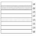
도 1은 본 발명의 일 실시예에 따른 유기 발광 표시 장치를 나타내는 단면도이고, 도 2는 도 1의 유기 발광 소자의 일부를 확대한 부분 단면도이다.FIG. 1 is a cross-sectional view illustrating an organic light emitting diode display according to an exemplary embodiment, and FIG. 2 is an enlarged partial cross-sectional view of a portion of the organic light emitting diode of FIG. 1 .
도 1 및 도 2를 참고하면, 본 발명의 일 실시예에 따른 유기 발광 표시 장치는 기판(123), 박막 트랜지스터(130), 제 1 전극(160), 제1 층(171, 172), 버퍼층(200), 발광층(173), 제2 층(174, 175), 제2 전극(180)을 포함한다.1 and 2 , an organic light emitting diode display according to an embodiment of the present invention includes a
제1 층(171, 172)은 정공 주입층(171) 및 정공 수송층(172)을 포함할 수 있고, 제2 층(174, 175)은 전자 수송층(174) 및 전자 주입층(175)을 포함할 수 있다.The
제1 전극(160)은 애노드(anode) 전극, 제2 전극(180)은 캐소드(cathode) 전극일 수 있으나, 이와 반대로 제1 전극(160)이 캐소드 전극이고 제2 전극(180)이 애노드 전극일 수 있다.The
이때, 기판(123)은 유리, 석영, 세라믹, 플라스틱 등으로 이루어진 절연성 기판으로 형성된다. 그러나, 본 발명의 일 실시예는 이에 한정되지 않고, 기판(123)은 스테인리스 강 등으로 이루어진 금속성 기판으로 형성될 수 있으며, 폴리카보네이트, 폴리메틸메타크릴레이트, 폴리에틸렌테레프탈레이트, 폴리에틸렌나프탈레이트, 폴리아미드, 폴리에테르술폰, 폴리이미드 또는 이들의 조합과 같은 유기 물질, 실리콘웨이퍼 등으로 만들어질 수도 있다.In this case, the
그리고, 기판(123) 위에는 기판 버퍼층(126)이 형성된다. 기판 버퍼층(126)은 불순 원소의 침투를 방지하며, 표면을 평탄화하는 역할을 한다.In addition, a
이때, 기판 버퍼층(126)은 상기 기능을 수행할 수 있는 다양한 물질로 형성될 수 있다. 예를 들어, 기판 버퍼층(126)은 질화 규소(SiNx)막, 산화 규소(SiOy)막, 산질화 규소(SiOxNy)막 중 어느 하나가 사용될 수 있다. 그러나, 기판 버퍼층(126)은 반드시 필요한 구성은 아니며, 기판(123)의 종류 및 공정 조건에 따라 생략될 수도 있다.In this case, the
기판 버퍼층(126) 위에는 구동 반도체층(137)이 형성된다. 구동 반도체층(137)은 다결정 규소막으로 형성된다. 또한, 구동 반도체층(137)은 불순물이 도핑되지 않은 채널 영역(135), 채널 영역(135)의 양 옆으로 도핑되어 형성된 소스 영역(134) 및 드레인 영역(136)을 포함한다. 이때, 도핑되는 이온 물질은 붕소(B)와 같은 P형 불순물이며, 주로 B2H6이 사용된다. 여기서, 이러한 불순물은 박막 트랜지스터의 종류에 따라 달라진다.A
구동 반도체층(137) 위에는 질화 규소(SiNx) 또는 산화 규소(SiOy) 따위로 형성된 게이트 절연막(127)이 형성된다. 게이트 절연막(127) 위에는 구동 게이트 전극(133)을 포함하는 게이트 배선이 형성된다. 그리고, 구동 게이트 전극(133)은 구동 반도체층(137)의 적어도 일부, 특히 채널 영역(135)와 중첩되도록 형성된다.A
한편, 게이트 절연막(127) 상에는 구동 게이트 전극(133)을 덮는 층간 절연막(128)이 형성된다. 게이트 절연막(127)과 층간 절연막(128)에는 구동 반도체층(137)의 소스 영역(134) 및 드레인 영역(136)을 드러내는 제1 접촉 구멍(122a) 및 제2 접촉 구멍(122b)이 형성된다. 층간 절연막(128)은, 게이트 절연막(127)과 마찬가지로, 질화 규소(SiNx) 또는 산화 규소(SiOy) 등의 세라믹(ceramic) 계열의 소재를 사용하여 만들어질 수 있다.Meanwhile, an
그리고, 층간 절연막(128) 위에는 구동 소스 전극(131) 및 구동 드레인 전극(132)을 포함하는 데이터 배선이 형성된다. 또한, 구동 소스 전극(131) 및 구동 드레인 전극(132)은 각각 층간 절연막(128) 및 게이트 절연막(127)에 형성된 제1 접촉 구멍(122a) 및 제2 접촉 구멍(122b)을 통해 구동 반도체층(137)의 소스 영역(134) 및 드레인 영역(136)과 연결된다.A data line including a
이와 같이, 구동 반도체층(137), 구동 게이트 전극(133), 구동 소스 전극(131) 및 구동 드레인 전극(132)을 포함하여 구동 박막 트랜지스터(130)가 형성된다. 구동 박막 트랜지스터(130)의 구성은 전술한 예에 한정되지 않고, 당해 기술 분야의 전문가가 용이하게 실시할 수 있는 공지된 구성으로 다양하게 변경 가능하다.As described above, the driving
그리고, 층간 절연막(128) 상에는 데이터 배선을 덮는 평탄화막(124)이 형성된다. 평판화막(124)은 그 위에 형성될 유기 발광 소자의 발광 효율을 높이기 위해 단차를 없애고 평탄화시키는 역할을 한다. 또한, 평탄화막(124)은 드레인 전극(132)의 일부를 노출시키는 제3 접촉 구멍(122c)을 갖는다.A
평탄화막(124)은 아크릴계 수지(polyacrylates resin), 에폭시 수지(epoxy resin), 페놀 수지(phenolic resin), 폴리아미드계 수지(polyamides resin), 폴리이미드계 수지(polyimides rein), 불포화 폴리에스테르계 수지(unsaturated polyesters resin), 폴리페닐렌계 수지(poly phenylenethers resin), 폴리페닐렌설파이드계 수지(poly phenylenesulfides resin), 및 벤조사이클로부텐(benzocyclobutene, BCB) 중 하나 이상의 물질 등으로 만들 수 있다.The
여기에서, 본 발명에 따른 일 실시예는 전술한 구조에 한정되는 것은 아니며, 경우에 따라 평탄화막(124)과 층간 절연막(128) 중 어느 하나는 생략될 수도 있다.Here, an embodiment according to the present invention is not limited to the above-described structure, and in some cases, any one of the
이때, 평탄화막(124) 위에는 유기 발광 소자의 제 1 전극(160), 즉 화소 전극(160)이 형성된다. 즉, 유기 발광 표시 장치는 복수의 화소들마다 각각 배치된 복수의 화소 전극(160)을 포함한다. 이때, 복수의 화소 전극(160)은 서로 이격 배치된다. 화소 전극(160)은 평탄화막(124)의 제3 접촉 구멍(122c)을 통해 드레인 전극(132)과 연결된다.In this case, the
또한, 평탄화막(124) 위에는 화소 전극(160)을 드러내는 개구부를 갖는 화소 정의막(125)이 형성된다. 즉, 화소 정의막(125)은 각 화소마다 형성된 복수개의 개구부를 갖는다. 이때, 화소 정의막(125)에 의해 형성된 개구부마다 발광 소자층(170)이 형성될 수 있다. 이에 따라, 화소 정의막(125)에 의해 각각의 유기 발광층이 형성되는 화소 영역이 정의될 수 있다.Also, a
이때, 화소 전극(160)은 화소 정의막(125)의 개구부에 대응하도록 배치된다. 그러나, 화소 전극(160)은 반드시 화소 정의막(125)의 개구부에만 배치되는 것은 아니며, 화소 전극(160)의 일부가 화소 정의막(125)과 중첩되도록 화소 정의막(125) 아래에 배치될 수 있다.In this case, the
화소 정의막(125)은 폴리아크릴계 수지(polyacrylates resin) 및 폴리이미드계(polyimides) 등의 수지 또는 실리카 계열의 무기물 등으로 만들 수 있다.The
한편, 화소 전극(160) 위에는 발광 소자층(170)이 형성된다. 발광 소자층(170)의 구조에 대해서는 하기에서 상세히 설명하기로 한다.Meanwhile, the light emitting
그리고, 발광 소자층(170) 상에는 제 2 전극(180), 즉 공통 전극(180)이 형성될 수 있다. 이와 같이, 화소 전극(160), 발광 소자층(170) 및 공통 전극(180)을 포함하는 유기 발광 소자(LD)가 형성된다.In addition, the
이때, 화소 전극(160) 및 공통 전극(180)은 각각 투명한 도전성 물질로 형성되거나 반투과형 또는 반사형 도전성 물질로 형성될 수 있다. 화소 전극(160) 및 공통 전극(180)을 형성하는 물질의 종류에 따라, 유기 발광 표시 장치는 전면 발광형, 배면 발광형 또는 양면 발광형이 될 수 있다.In this case, each of the
한편, 공통 전극(180) 위에는 공통 전극(180)을 덮어 보호하는 덮개막(190)이 유기막으로 형성될 수 있다.Meanwhile, an
그리고, 덮개막(190) 위에는 박막 봉지층(121)이 형성되어 있다. 박막 봉지층(121)은 기판(123) 위에 형성되어 있는 유기 발광 소자(LD)와 구동 회로부를 외부로부터 밀봉시켜 보호한다.In addition, a thin
박막 봉지층(121)은 서로 하나씩 교대로 적층되는 봉지 유기막(121a, 121c)과 봉지 무기막(173, 121d)을 포함한다. 도 1에서는 일례로 2개의 봉지 유기막(121a, 121c)과 2개의 봉지 무기막(173, 121d)이 하나씩 교대로 적층되어 박막 봉지층(121)을 구성하는 경우를 도시하였으나, 이에 한정되지 않는다.The thin
이제부터 도 2를 참고하여 본 발명의 유기 발광 소자에 대해서 상세하게 설명한다. 도 2는 도 1의 유기 발광 소자의 일부를 확대한 부분 단면도이다.Hereinafter, the organic light emitting device of the present invention will be described in detail with reference to FIG. 2 . FIG. 2 is an enlarged partial cross-sectional view of a portion of the organic light emitting diode of FIG. 1 .
본 발명의 일 실시예에 따른 유기 발광 소자(도 1의 X 부분)는 제 1 전극(160), 정공 주입층(171), 정공 수송층(172), 발광층(173), 전자 수송층(174), 전자 주입층(175), 중간층(200) 및 제 2 전극(180)이 순서대로 적층된 구조이다.The organic light-emitting device (part X in FIG. 1 ) according to an embodiment of the present invention includes a
즉, 도 1의 발광 소자층(170)은 도 2의 정공 주입층(171), 정공 수송층(172), 발광층(173), 전자 수송층(174), 전자 주입층(175) 및 중간층(200)을 포함한다.That is, the light emitting
제1 전극(160)이 애노드(anode)일 경우에는 정공 주입이 용이하도록 높은 일 함수를 갖는 물질 중에서 선택된 물질을 포함할 수 있다.When the
본 발명의 일 실시예에 따른 제1 전극(160)은 투명 전극으로서, 인듐 주석 산화물(ITO), 인듐 아연 산화물(IZO), 주석 산화물(SnO2), 아연 산화물(ZnO) 또는 이들의 조합과 같은 도전성 산화물 또는 알루미늄(Al), 은(Ag), 마그네슘(Mg)과 같은 금속을 사용하여 얇은 두께로 형성될 수 있다. 또한, 제1 전극(160)은 이에 한정되지 않으며, 도전성 산화물과 금속 물질의 2층 이상의 적층 구조로 형성될 수도 있다.The
정공 주입층(171)은 제 1 전극(160) 위에 배치될 수 있다. 이때, 정공 주입층(171)은 제 1 전극(160)으로부터 정공 수송층(172)으로의 정공의 주입을 개선하는 기능을 수행할 수 있다. 정공 주입층(171)은 금속 또는 비금속과 할로겐 원소인 F, Cl, Br, I 등이 조합된 쌍극자 물질을 포함할 수 있다. 하지만 정공 주입층(171)은 이에 한정되지 않고 다른 무기 물질 또는 유기 물질로 형성할 수도 있다.The
금속 또는 비금속은 Ag, Au, B, Be, C, Co, Cr, Cu, Fe, Hg, Ir, Mo, Nb, Ni, Os, Pd, Pt, Re, Rh, Ru, Sb, Se, Si, Sn, Ta, Te, Ti, V, W 및 Zn 중에서 선택된 적어도 하나의 원소일 수 있다.Metals or nonmetals are Ag, Au, B, Be, C, Co, Cr, Cu, Fe, Hg, Ir, Mo, Nb, Ni, Os, Pd, Pt, Re, Rh, Ru, Sb, Se, Si, It may be at least one element selected from Sn, Ta, Te, Ti, V, W, and Zn.
정공 주입층(171)은 CuI(copper iodide), CoI2(cobalt iodide), CuPc(copper phthalocyanine) 등을 포함할 수 있으나, 이에 한정되는 것은 아니다.The
정공 주입층(171)의 두께는 25 ~ 35 nm 일 수 있다.The thickness of the
정공 수송층(172)은 정공 주입층(171) 상에 배치될 수 있다. 정공 수송층(172)은 정공 주입층(171)으로부터 전달되는 정공을 원활하게 수송하는 기능을 수행할 수 있다. 예를 들면, 정공 수송층(172)은 NPD(N,N-dinaphthyl-N,N'-diphenyl benzidine), TPD(N,N'-bis-(3-methylphenyl)-N,N'-bis-(phenyl)-benzidine), s-TAD, MTDATA(4,4',4"-Tris(N-3-methylphenyl-N-phenyl-amino)-triphenylamine) 등을 포함할 수 있으나, 이에 한정되는 것은 아니다.The
한편, 정공 주입층(171)은 정공 수송층(172)에 포함된 재료와 동일한 물질에 P타입의 도펀트(dopant)가 적용된 물질을 포함하여 유기 발광 소자의 구동 전압을 감소시켜 정공 주입 특성을 향상시킬 수 있다.On the other hand, the
이때, 정공 수송층(172)의 두께는 15 ~ 25 nm 일 수 있다.In this case, the thickness of the
본 실시예에서 정공 주입층(171)과 정공 수송층(172)이 적층된 구조를 형성되는 것으로 설명하였으나, 이에 한정되지 않고 정공 주입층(171) 및 정공 수송층(172)은 단일층으로 형성될 수도 있다.In the present embodiment, it has been described that a structure in which the
정공 수송층(172) 위에 발광층(173)이 형성된다. 발광층(173)은 특정 색을 표시하는 발광 물질을 포함한다. 예를 들어, 발광층(173)은 청색, 녹색 또는 적색과 같은 기본색 또는 이들을 조합하는 색을 표시할 수 있다.An
이때, 발광층(173)의 두께는 10 ~ 50 nm일 수 있다.In this case, the thickness of the
발광층(173)은 호스트와 도펀트를 포함한다. 발광층(173)은 적색, 녹색, 청색 및 백색을 발광하는 물질을 포함할 수 있으며, 인광 또는 형광물질을 이용하여 형성할 수 있다.The
발광층(173)이 적색을 발광하는 경우, CBP(carbazole biphenyl) 또는 mCP(1,3-bis(carbazol-9-yl)를 포함하는 호스트 물질을 포함하며, PIQIr(acac)(bis(1-phenylisoquinoline)acetylacetonate iridium), PQIr(acac)(bis(1-phenylquinoline)acetylacetonate iridium), PQIr(tris(1-phenylquinoline)iridium) 및 PtOEP(octaethylporphyrin platinum) 중에서 선택된 적어도 하나를 포함하는 도펀트를 포함하는 인광물질로 이루어질 수 있고, 이와는 달리 PBD:Eu(DBM)3(Phen) 또는 Perylene을 포함하는 형광물질로 이루어질 수 있으나 이에 한정되지 않는다.When the
발광층(173)이 녹색을 발광하는 경우, CBP 또는 mCP를 포함하는 호스트 물질을 포함하며, Ir(ppy)3(fac-tris(2-phenylpyridine)iridium)을 포함하는 도펀트 물질을 포함하는 인광물질로 이루어질 수 있고, 이와는 달리, Alq3(tris(8-hydroxyquinolino)aluminum)을 포함하는 형광물질로 이루어질 수 있으나 이에 한정되지 않는다.When the
발광층(173)이 청색을 발광하는 경우, CBP, 또는 mCP를 포함하는 호스트 물질을 포함하며, (4,6-F2ppy)2Irpic 를 포함하는 도펀트 물질을 포함하는 인광물질로 이루어질 수 있다. 이와는 달리, spiro-DPVBi, spiro-6P, 디스틸벤젠(DSB), 디스트릴아릴렌(DSA), PFO계 고분자 및 PPV계 고분자로 이루어진 군에서 선택된 어느 하나를 포함하는 형광물질로 이루어질 수 있으나 이에 한정되지 않는다.When the
한편, 발광층(173) 위에 전자 수송층(174)이 배치될 수 있다. 이때, 전자 수송층(174)은 제 2 전극(180)으로부터 발광층(173)으로 전자를 전달할 수 있다. 또한, 전자 수송층(174)은 제 1 전극(160)으로부터 주입된 정공이 발광층(173)을 통과하여 제 2 전극(180)으로 이동하는 것을 방지할 수 있다. 즉, 전자 수송층(174)은 정공 저지층의 역할을 하여, 발광층(173)에서 정공과 전자의 결합을 돕는다.Meanwhile, an
이때, 전자 수송층(174)은 Alq3(tris(8-hydroxyquinolino)aluminum), PBD, TAZ, spiro-PBD, BAlq 및 SAlq로 이루어진 군에서 선택된 어느 하나 이상으로 이루어질 수 있으나, 이에 한정되지 않는다.In this case, the
전자 수송층(174) 위에는 전자 주입층(175)이 형성되어 있다. 전자 주입층(175)은 제2 전극(180)으로부터 전자 수송층(174)으로의 전자의 주입을 개선하는 기능을 수행할 수 있다.An
본 발명의 일 실시에에 따른 전자 주입층(175)은 금속 기반의 할로겐 쌍극자 물질을 포함한다. 전자 주입층(175)은 바람직하게는 1족, 2족, 란탄계 금속(lanthanide metal)으로서 Li, Na, K, Rb, Cs, Fr, Be, Mg, Ca, Sr, Ba, Ra, La, Yb, Lu, Tm, Ce, Pr 및 Nd 중 선택된 어느 하나의 물질에 할로겐 원소인 F, Cl, Br 및 I 중 선택된 어느 하나의 물질이 결합된 쌍극자 물질일 수 있다.The
전자 주입층(175)은 금속 기반의 할로겐 쌍극자 물질의 단일층으로 형성하거나, 금속 및 금속 기반의 할로겐 물질을 포함한 2층의 구조로 형성할 수 있다.The
전자 주입층(175)은 스퍼터링(sputtering)법을 이용해서 형성할 수 있다.The
전자 주입층(175) 위에는 중간층(200)이 형성된다. 중간층(200)은 뒤이어 설명할 제2 전극(180)과 전자 주입층(175) 사이에서 계면 저항을 감소시켜 주고, 제2 전극(180)의 표면이 균일하게 형성될 수 있도록 하는 역할을 한다.The
즉, 중간층(200)은 제2 전극(180)과 전자 주입층(175) 사이의 계면 저항을 감소시켜 제2 전극(180)에서 전자 주입층(175)으로의 전자 주입이 원활히 일어날 수 있도록 하는 이온 전도체(ionic conductor) 역할을 할 수 있다.That is, the
중간층(200)은 1족, 2족, 란탄계 금속 및 전이금속 중 적어도 하나의 원소를 포함하는 제1 물질 및 할로겐을 포함하는 제2 물질로 형성된 쌍극자 물질일 수 있다. 이 때, 제1 물질은 1족, 2족, 란탄계 금속 중 하나의 원소 및 전이 금속 중 적어도 하나의 원소를 포함할 수 있고, 바람직하게는 본 실시예에 따른 중간층(200)은 제1 물질 및 제2 물질을 포함하는 3원계 쌍극자 물질일 수 있다.The
여기서 1족, 2족, 란탄계 금속으로서, Li, Na, K, Rb, Cs, Fr, Be, Mg, Ca, Sr, Ba, Ra, La, Yb, Lu, Tm, Ce, Pr 또는 Nd 등을 포함할 수 있다.Here, as a Group 1, 2, or lanthanide-based metal, Li, Na, K, Rb, Cs, Fr, Be, Mg, Ca, Sr, Ba, Ra, La, Yb, Lu, Tm, Ce, Pr or Nd, etc. may include
구체적으로, 중간층(200)은 삼원계 무기 쌍극자일 수 있으며, 그 예시로서 LiAg4I5, NaAg4I5, KAg4I5, RbAg4I5, CsAg4I5, LiCu4I5, NaCu4I5, KCu4I5, RbCu4I5 및 CsCu4I5중 선택된 어느 하나 이상의 화합물을 포함할 수 있으나, 이에 한정되지 않는다.Specifically, the
중간층(200)의 두께는 10~ 200Å의 범위를 가지는 것이 바람직한데, 10Å 미만일 경우 중간층(200)의 효과가 미비할 수 있으며, 200Å 초과일 경우 중간층(200)으로 인해 전자 주입층(175)으로의 전자 주입에 문제가 발생할 수 있기 때문이다.The thickness of the
중간층(200)은 열증발법을 이용해서 형성할 수 있어 저온에서도 형성할 수 있다. 그러나, 이에 한정되지 않으며, 중간층(200)은 스퍼터링(sputtering)법, 화학기상증착(CVD; chemical vapor deposition), 원자층 증착(ALD; atomic layer deposition), Chemical solution 증착법(CSD) 등 다양한 방법으로 형성할 수 있다.The
중간층(200) 위에는 제2 전극(180)이 형성된다. 본 발명의 일 실시예에 따른 유기 발광 표시 장치는 제1 전극(160)이 애노드(anode)인 경우로서, 제2 전극(180)은 캐소드(cathode)일 수 있다. 제2 전극(180) 역시 투명 전극으로서, 인듐 주석 산화물(ITO), 인듐 아연 산화물(IZO), 주석 산화물(SnO2), 아연 산화물(ZnO) 또는 이들의 조합과 같은 도전성 산화물 또는 알루미늄(Al), 은(Ag), 마그네슘(Mg)과 같은 금속을 사용하여 얇은 두께로 형성될 수 있다. 또한, 제1 전극(160)은 이에 한정되지 않으며, 도전성 산화물과 금속 물질의 2층 이상의 적층 구조로 형성될 수도 있다.The
이하에서는, 도 3 및 도 4를 참고하여 본 발명의 다른 실시예에 따른 유기 발광 표시 장치에 대해서 설명한다.Hereinafter, an organic light emitting diode display according to another exemplary embodiment of the present invention will be described with reference to FIGS. 3 and 4 .
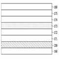
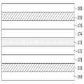
도 3은 본 발명의 다른 실시예에 따른 유기 발광 소자의 일부를 확대한 부분 단면도이고, 도 4는 본 발명의 또 다른 실시예에 따른 유기 발광 소자의 일부를 확대한 부분 단면도이다.3 is an enlarged partial cross-sectional view of a part of an organic light emitting diode according to another embodiment of the present invention, and FIG. 4 is an enlarged partial cross-sectional view of a part of the organic light emitting diode according to another embodiment of the present invention.
도 3 및 도 4에 나타낸 본 발명의 다른 실시예 및 또 다른 실시예에 따른 유기 발광 표시 장치는 앞서 도 2에서 설명한 실시예에 따른 유기 발광 표시 장치와 비교하여 중간층(200)의 위치를 제외하고는 동일한 바, 중복되는 설명은 생략한다.3 and 4 , the organic light emitting diode display according to another embodiment and another embodiment of the present invention is compared with the organic light emitting diode display according to the embodiment described with reference to FIG. 2 , except for the position of the
먼저, 도 3에 나타낸 본 발명의 다른 실시예에 따른 유기 발광 표시 장치에 대해서 살펴본다.First, an organic light emitting diode display according to another exemplary embodiment shown in FIG. 3 will be described.
도 3에 나타난 바와 같이, 본 발명의 다른 실시예에 따른 유기 발광 표시 장치의 중간층(200)은 제1 전극(160)과 정공 주입층(171) 사이에 형성되어 있다.3 , the
본 실시예에 따른 중간층(200)은 앞서 도 2의 실시예에서 설명한 중간층(200)에 관한 내용이 대부분 적용될 수 있으며, 여기서 중간층(200)은 제1 전극(160)과 정공 주입층(171)의 계면 저항을 감소시켜 정공 주입이 원활히 이루어질 수 있도록 하는 이온 전도체 역할을 할 수 있다.As for the
다음으로, 도 4에 나타낸 본 발명의 또 다른 실시예에 따른 유기 발광 표시 장치의 중간층(200)은 제1 전극(160)과 정공 주입층(171) 사이 및 제2 전극(180)과 전자 주입층(175) 사이에 모두 형성되어 있다.Next, the
이 경우, 중간층(200)은 제1 전극(160)과 정공 주입층(171)의 계면 저항뿐만 아니라 제2 전극(180)과 전자 주입층(175)의 계면 저항을 감소시켜 정공 및 전자 주입이 원활히 이루어질 수 있도록 하는 이온 전도체 역할을 할 수 있다.In this case, the
이상과 같이 본 발명의 실시예에 따르면, 전극과 발광층 사이에 이온 전도체 물질을 포함하는 중간층을 형성하여 전극의 계면 저항을 감소시키고 표면을 균일하게 형성할 수 있어, 유기 발광 표시 장치의 발광 효율을 증가시킬 수 있다.As described above, according to the embodiment of the present invention, an intermediate layer including an ion conductor material is formed between the electrode and the light emitting layer to reduce the interfacial resistance of the electrode and uniformly form the surface, thereby improving the luminous efficiency of the organic light emitting display device. can increase
이상에서 본 발명의 바람직한 실시예에 대하여 상세하게 설명하였지만 본 발명의 권리범위는 이에 한정되는 것은 아니고 다음의 청구범위에서 정의하고 있는 본 발명의 기본 개념을 이용한 당업자의 여러 변형 및 개량 형태 또한 본 발명의 권리범위에 속하는 것이다.Although the preferred embodiment of the present invention has been described in detail above, the scope of the present invention is not limited thereto, and various modifications and improvements by those skilled in the art using the basic concept of the present invention as defined in the following claims are also provided. is within the scope of the
123: 기판130: 박막 트랜지스터
160: 제 1 전극180: 제 2 전극
171: 정공 주입층172: 정공 수송층
173: 발광층174: 전자 수송층
175: 전자 주입층200: 중간층123: substrate 130: thin film transistor
160: first electrode 180: second electrode
171: hole injection layer 172: hole transport layer
173: light emitting layer 174: electron transport layer
175: electron injection layer 200: intermediate layer
Claims (16)
Translated fromKorean상기 기판 위에 위치하는 박막 트랜지스터,
상기 박막 트랜지스터와 전기적으로 연결되어 있는 제1 전극,
상기 제1 전극 위에 위치하는 정공 주입층,
상기 정공 주입층 위에 위치하는 발광층,
상기 발광층 위에 위치하는 전자 주입층,
상기 전자 주입층 위에 위치하는 제1 중간층, 및
상기 제1 중간층 위에 위치하는 제2 전극을 포함하며,
상기 제1 중간층은 1족, 2족, 란탄계 금속 및 전이 금속 중 적어도 하나의 원소를 포함하는 제1 물질 및 할로겐을 포함하는 제2 물질로 형성된 쌍극자 물질을 포함하고,
상기 제1 전극 및 상기 제1 중간층 사이에 위치하는 제2 중간층을 포함하며,
상기 제2 중간층은 1족, 2족, 란탄계 금속 및 전이 금속 중 적어도 하나의 원소를 포함하는 제3 물질 및 할로겐을 포함하는 제4 물질로 형성된 쌍극자 물질을 포함하는 유기 발광 표시 장치.Board,
a thin film transistor positioned on the substrate;
a first electrode electrically connected to the thin film transistor;
a hole injection layer positioned on the first electrode;
a light emitting layer positioned on the hole injection layer;
an electron injection layer positioned on the light emitting layer;
a first intermediate layer overlying the electron injection layer; and
a second electrode positioned on the first intermediate layer;
The first intermediate layer includes a dipole material formed of a first material including at least one element of Group 1, Group 2, a lanthanide metal, and a transition metal, and a second material including a halogen,
a second intermediate layer positioned between the first electrode and the first intermediate layer;
The second intermediate layer includes a dipole material formed of a third material including at least one of Group 1, Group 2, a lanthanide-based metal, and a transition metal, and a fourth material including a halogen.
상기 제1 물질은 1족, 2족, 란탄계 금속 중 하나의 원소, 및
전이 금속 중 하나의 원소를 포함하는 유기 발광 표시 장치.In claim 1,
The first material is an element of one of Group 1, Group 2, and a lanthanide metal, and
An organic light emitting diode display including one of transition metals.
상기 제1 중간층은 삼원계 무기 쌍극자 물질을 포함하는 유기 발광 표시 장치.In claim 2,
and the first intermediate layer includes a ternary inorganic dipole material.
상기 제1 중간층은 LiAg4I5, NaAg4I5, KAg4I5, RbAg4I5, CsAg4I5, LiCu4I5, NaCu4I5, KCu4I5, RbCu4I5 및 CsCu4I5중 선택된 적어도 하나의 화합물을 포함하는 유기 발광 표시 장치.In claim 3,
The first intermediate layer is LiAg4 I5 , NaAg4 I5 , KAg4 I5 , RbAg4 I5 , CsAg4 I5 , LiCu4 I5 , NaCu4 I5 , KCu4 I5 , RbCu4 I5 , and CsCu4 I5An organic light emitting diode display including at least one compound selected from among
상기 제1 중간층의 두께는 10~200Å의 범위로 형성된 유기 발광 표시 장치.In claim 3,
The thickness of the first intermediate layer is in the range of 10 to 200 Å.
상기 전자 주입층은 금속 기반의 할로겐 쌍극자 물질을 포함하는 유기 발광 표시 장치.In claim 1,
The electron injection layer includes a metal-based halogen dipole material.
상기 전자 주입층에 포함되는 상기 금속은 1족, 2족 또는 란탄계 금속 중 선택된 어느 하나 이상의 물질을 포함하는 유기 발광 표시 장치.In claim 6,
The metal included in the electron injection layer includes at least one material selected from Group 1, Group 2, and/or lanthanide-based metals.
상기 정공 주입층은 금속 또는 비금속 기반의 할로겐 쌍극자 물질을 포함하는 유기 발광 표시 장치.In claim 6,
The hole injection layer includes a metal or non-metal-based halogen dipole material.
상기 정공 주입층에 포함되는 상기 금속 또는 비금속은 Ag, Au, B, Be, C, Co, Cr, Cu, Fe, Hg, Ir, Mo, Nb, Ni, Os, Pd, Pt, Re, Rh, Ru, Sb, Se, Si, Sn, Ta, Te, Ti, V, W 및 Zn 중 선택된 적어도 하나의 물질을 포함하는 유기 발광 표시 장치.In claim 8,
The metal or non-metal included in the hole injection layer is Ag, Au, B, Be, C, Co, Cr, Cu, Fe, Hg, Ir, Mo, Nb, Ni, Os, Pd, Pt, Re, Rh, An organic light emitting diode display comprising at least one material selected from Ru, Sb, Se, Si, Sn, Ta, Te, Ti, V, W, and Zn.
제3 물질은 1족, 2족, 란탄계 금속 중 하나의 원소, 및
전이 금속 중 하나의 원소를 포함하는 유기 발광 표시 장치.In claim 1,
The third material is an element of one of Groups 1, 2, and lanthanide metals, and
An organic light emitting diode display including one of transition metals.
상기 제1 중간층 및 상기 제2 중간층은 동일한 물질을 포함하는 유기 발광 표시 장치.In claim 1,
The first intermediate layer and the second intermediate layer include the same material.
상기 제1 중간층 및 상기 제2 중간층은 삼원계 무기 쌍극자 물질을 포함하며,
상기 삼원계 무기 쌍극자 물질은 LiAg4I5, NaAg4I5, KAg4I5, RbAg4I5, CsAg4I5, LiCu4I5, NaCu4I5, KCu4I5, RbCu4I5 및 CsCu4I5중 선택된 적어도 하나의 화합물인 유기 발광 표시 장치.In claim 12,
The first intermediate layer and the second intermediate layer include a ternary inorganic dipole material,
The ternary inorganic dipole material is LiAg4 I5 , NaAg4 I5 , KAg4 I5 , RbAg4 I5 , CsAg4 I5 , LiCu4 I5 , NaCu4 I5 , KCu4 I5 , RbCu4 I5 and CsCu4 I5at least one compound selected from among organic light emitting diodes.
상기 기판 위에 위치하는 박막 트랜지스터,
상기 박막 트랜지스터와 전기적으로 연결되어 있는 제1 전극,
상기 제1 전극 위에 위치하는 중간층,
상기 중간층 위에 위치하는 정공 주입층,
상기 정공 주입층 위에 위치하는 발광층,
상기 발광층 위에 위치하는 전자 주입층,
상기 전자 주입층 위에 위치하는 제2 전극을 포함하며,
상기 중간층은 1족, 2족, 란탄계 금속 및 전이 금속 중 적어도 하나의 원소를 포함하는 제1 물질 및 할로겐을 포함하는 제2 물질로 형성된 삼원계 무기 쌍극자 물질을 포함하는 유기 발광 표시 장치.Board,
a thin film transistor positioned on the substrate;
a first electrode electrically connected to the thin film transistor;
an intermediate layer positioned on the first electrode;
a hole injection layer located on the intermediate layer;
a light emitting layer positioned on the hole injection layer;
an electron injection layer positioned on the light emitting layer;
a second electrode positioned on the electron injection layer;
The intermediate layer includes a ternary inorganic dipole material formed of a first material including at least one of Group 1, Group 2, a lanthanide-based metal, and a transition metal, and a second material including a halogen.
상기 제1 물질은 1족, 2족, 란탄계 금속 중 하나의 원소, 및
전이 금속 중 하나의 원소를 포함하는 유기 발광 표시 장치.15. In claim 14,
The first material is an element of one of Group 1, Group 2, and a lanthanide metal, and
An organic light emitting diode display including one of transition metals.
상기 삼원계 무기 쌍극자 물질은 LiAg4I5, NaAg4I5, KAg4I5, RbAg4I5, CsAg4I5, LiCu4I5, NaCu4I5, KCu4I5, RbCu4I5 및 CsCu4I5중 선택된 적어도 하나의 화합물인 유기 발광 표시 장치.
In claim 15,
The ternary inorganic dipole material is LiAg4 I5 , NaAg4 I5 , KAg4 I5 , RbAg4 I5 , CsAg4 I5 , LiCu4 I5 , NaCu4 I5 , KCu4 I5 , RbCu4 I5 and at least one compound selected from CsCu4 I5 .
Priority Applications (2)
| Application Number | Priority Date | Filing Date | Title |
|---|---|---|---|
| KR1020150074879AKR102447308B1 (en) | 2015-05-28 | 2015-05-28 | organic light emitting diode display |
| US15/013,710US9608227B2 (en) | 2015-05-28 | 2016-02-02 | Organic light emitting diode display |
Applications Claiming Priority (1)
| Application Number | Priority Date | Filing Date | Title |
|---|---|---|---|
| KR1020150074879AKR102447308B1 (en) | 2015-05-28 | 2015-05-28 | organic light emitting diode display |
Publications (2)
| Publication Number | Publication Date |
|---|---|
| KR20160141129A KR20160141129A (en) | 2016-12-08 |
| KR102447308B1true KR102447308B1 (en) | 2022-09-26 |
Family
ID=57399157
Family Applications (1)
| Application Number | Title | Priority Date | Filing Date |
|---|---|---|---|
| KR1020150074879AActiveKR102447308B1 (en) | 2015-05-28 | 2015-05-28 | organic light emitting diode display |
Country Status (2)
| Country | Link |
|---|---|
| US (1) | US9608227B2 (en) |
| KR (1) | KR102447308B1 (en) |
Families Citing this family (6)
| Publication number | Priority date | Publication date | Assignee | Title |
|---|---|---|---|---|
| EP3168886B8 (en)* | 2015-11-10 | 2023-07-26 | Novaled GmbH | Metallic layer comprising alkali metal and second metal |
| EP3168894B8 (en)* | 2015-11-10 | 2023-07-26 | Novaled GmbH | N-doped semiconducting material comprising two metal dopants |
| KR102708001B1 (en)* | 2017-02-15 | 2024-09-20 | 삼성디스플레이 주식회사 | Light emitting diode and display device including the same |
| KR20200072647A (en)* | 2018-12-12 | 2020-06-23 | 삼성디스플레이 주식회사 | Organic electroluminescence device and display device including the same |
| KR102798335B1 (en)* | 2019-02-18 | 2025-04-23 | 삼성디스플레이 주식회사 | Luminescence device, and display device including the same |
| CN111341942B (en)* | 2020-02-11 | 2023-03-03 | 郑州大学 | A kind of electric injection yellow light LED based on lead-free copper-based iodide and its preparation method |
Family Cites Families (11)
| Publication number | Priority date | Publication date | Assignee | Title |
|---|---|---|---|---|
| US3443997A (en)* | 1966-02-11 | 1969-05-13 | North American Rockwell | Solid state electrochemical devices |
| US3476606A (en)* | 1967-07-06 | 1969-11-04 | North American Rockwell | Solid state electrochemical device |
| US3476605A (en)* | 1967-07-06 | 1969-11-04 | North American Rockwell | Solid state electric cell utilizing as an electron acceptor material an organic ammonium polyiodide |
| US5677572A (en) | 1996-07-29 | 1997-10-14 | Eastman Kodak Company | Bilayer electrode on a n-type semiconductor |
| KR20080011623A (en) | 2006-07-31 | 2008-02-05 | 엘지전자 주식회사 | Electroluminescent element and manufacturing method thereof |
| KR100994116B1 (en)* | 2008-08-20 | 2010-11-15 | 삼성모바일디스플레이주식회사 | Organic light emitting device |
| DE102008053121A1 (en)* | 2008-10-24 | 2010-04-29 | Merck Patent Gmbh | Double complex salts as emitters in OLED devices |
| KR101677265B1 (en)* | 2010-03-31 | 2016-11-18 | 삼성디스플레이 주식회사 | Organic light emitting diode display |
| KR101182447B1 (en) | 2010-06-16 | 2012-09-12 | 삼성디스플레이 주식회사 | Organic light emitting device and manufacturing method thereof |
| JP5982747B2 (en) | 2010-07-21 | 2016-08-31 | 住友化学株式会社 | Organic EL device |
| TWI490211B (en)* | 2011-12-23 | 2015-07-01 | Semiconductor Energy Lab | Organometallic complex, light-emitting element, light-emitting device, electronic device and lighting device |
- 2015
- 2015-05-28KRKR1020150074879Apatent/KR102447308B1/enactiveActive
- 2016
- 2016-02-02USUS15/013,710patent/US9608227B2/enactiveActive
Also Published As
| Publication number | Publication date |
|---|---|
| US9608227B2 (en) | 2017-03-28 |
| KR20160141129A (en) | 2016-12-08 |
| US20160351845A1 (en) | 2016-12-01 |
Similar Documents
| Publication | Publication Date | Title |
|---|---|---|
| KR101733151B1 (en) | Organic light emitting diode and organic light emitting display device including the same | |
| KR102407115B1 (en) | Organic light emitting diode display | |
| US9960380B2 (en) | Organic light emitting diode and organic light emitting display device including the same | |
| KR102483892B1 (en) | Organic light emitting diode display | |
| KR102277378B1 (en) | Organic light emitting diode and organic light emitting display device including the same | |
| KR102447308B1 (en) | organic light emitting diode display | |
| KR102343279B1 (en) | Organic light emitting diode and organic light emitting display device including the same | |
| KR102392044B1 (en) | Organic light emitting diode and organic light emitting diode display including the same | |
| US10003040B2 (en) | Organic light emitting diode and organic light emitting display device including the same | |
| US9595688B2 (en) | Organic light emitting diode and organic light emitting display device including halogen dipole material | |
| US20160351819A1 (en) | Organic light emitting diode and organic light emitting diode display including the same | |
| US20090079333A1 (en) | Light-emitting device | |
| US9905792B2 (en) | Organic light emitting diode and organic light emitting diode display including the same | |
| US20160300893A1 (en) | Organic light emitting diode display | |
| KR102447311B1 (en) | Organic light emitting diode and organic light emitting display device including the same | |
| US10714559B2 (en) | Organic light emitting diode, method of manufacturing the same, and organic light emitting display including the same |
Legal Events
| Date | Code | Title | Description |
|---|---|---|---|
| PA0109 | Patent application | Patent event code:PA01091R01D Comment text:Patent Application Patent event date:20150528 | |
| PG1501 | Laying open of application | ||
| A201 | Request for examination | ||
| PA0201 | Request for examination | Patent event code:PA02012R01D Patent event date:20200416 Comment text:Request for Examination of Application Patent event code:PA02011R01I Patent event date:20150528 Comment text:Patent Application | |
| E902 | Notification of reason for refusal | ||
| PE0902 | Notice of grounds for rejection | Comment text:Notification of reason for refusal Patent event date:20210701 Patent event code:PE09021S01D | |
| E902 | Notification of reason for refusal | ||
| PE0902 | Notice of grounds for rejection | Comment text:Notification of reason for refusal Patent event date:20220121 Patent event code:PE09021S01D | |
| E701 | Decision to grant or registration of patent right | ||
| PE0701 | Decision of registration | Patent event code:PE07011S01D Comment text:Decision to Grant Registration Patent event date:20220713 | |
| GRNT | Written decision to grant | ||
| PR0701 | Registration of establishment | Comment text:Registration of Establishment Patent event date:20220921 Patent event code:PR07011E01D | |
| PR1002 | Payment of registration fee | Payment date:20220921 End annual number:3 Start annual number:1 | |
| PG1601 | Publication of registration |