KR102444680B1 - Binarization method and preform mask optimization flow - Google Patents
Binarization method and preform mask optimization flowDownload PDFInfo
- Publication number
- KR102444680B1 KR102444680B1KR1020207023649AKR20207023649AKR102444680B1KR 102444680 B1KR102444680 B1KR 102444680B1KR 1020207023649 AKR1020207023649 AKR 1020207023649AKR 20207023649 AKR20207023649 AKR 20207023649AKR 102444680 B1KR102444680 B1KR 102444680B1
- Authority
- KR
- South Korea
- Prior art keywords
- function
- pattern
- mask
- image
- cost function
- Prior art date
- Legal status (The legal status is an assumption and is not a legal conclusion. Google has not performed a legal analysis and makes no representation as to the accuracy of the status listed.)
- Active
Links
Images


Classifications
- G—PHYSICS
- G03—PHOTOGRAPHY; CINEMATOGRAPHY; ANALOGOUS TECHNIQUES USING WAVES OTHER THAN OPTICAL WAVES; ELECTROGRAPHY; HOLOGRAPHY
- G03F—PHOTOMECHANICAL PRODUCTION OF TEXTURED OR PATTERNED SURFACES, e.g. FOR PRINTING, FOR PROCESSING OF SEMICONDUCTOR DEVICES; MATERIALS THEREFOR; ORIGINALS THEREFOR; APPARATUS SPECIALLY ADAPTED THEREFOR
- G03F1/00—Originals for photomechanical production of textured or patterned surfaces, e.g., masks, photo-masks, reticles; Mask blanks or pellicles therefor; Containers specially adapted therefor; Preparation thereof
- G03F1/68—Preparation processes not covered by groups G03F1/20 - G03F1/50
- G03F1/70—Adapting basic layout or design of masks to lithographic process requirements, e.g., second iteration correction of mask patterns for imaging
- G—PHYSICS
- G03—PHOTOGRAPHY; CINEMATOGRAPHY; ANALOGOUS TECHNIQUES USING WAVES OTHER THAN OPTICAL WAVES; ELECTROGRAPHY; HOLOGRAPHY
- G03F—PHOTOMECHANICAL PRODUCTION OF TEXTURED OR PATTERNED SURFACES, e.g. FOR PRINTING, FOR PROCESSING OF SEMICONDUCTOR DEVICES; MATERIALS THEREFOR; ORIGINALS THEREFOR; APPARATUS SPECIALLY ADAPTED THEREFOR
- G03F1/00—Originals for photomechanical production of textured or patterned surfaces, e.g., masks, photo-masks, reticles; Mask blanks or pellicles therefor; Containers specially adapted therefor; Preparation thereof
- G03F1/36—Masks having proximity correction features; Preparation thereof, e.g. optical proximity correction [OPC] design processes
- G—PHYSICS
- G06—COMPUTING OR CALCULATING; COUNTING
- G06F—ELECTRIC DIGITAL DATA PROCESSING
- G06F30/00—Computer-aided design [CAD]
- G06F30/30—Circuit design
- G06F30/39—Circuit design at the physical level
- G06F30/398—Design verification or optimisation, e.g. using design rule check [DRC], layout versus schematics [LVS] or finite element methods [FEM]
- G—PHYSICS
- G06—COMPUTING OR CALCULATING; COUNTING
- G06F—ELECTRIC DIGITAL DATA PROCESSING
- G06F2119/00—Details relating to the type or aim of the analysis or the optimisation
- G06F2119/18—Manufacturability analysis or optimisation for manufacturability
- Y—GENERAL TAGGING OF NEW TECHNOLOGICAL DEVELOPMENTS; GENERAL TAGGING OF CROSS-SECTIONAL TECHNOLOGIES SPANNING OVER SEVERAL SECTIONS OF THE IPC; TECHNICAL SUBJECTS COVERED BY FORMER USPC CROSS-REFERENCE ART COLLECTIONS [XRACs] AND DIGESTS
- Y02—TECHNOLOGIES OR APPLICATIONS FOR MITIGATION OR ADAPTATION AGAINST CLIMATE CHANGE
- Y02P—CLIMATE CHANGE MITIGATION TECHNOLOGIES IN THE PRODUCTION OR PROCESSING OF GOODS
- Y02P90/00—Enabling technologies with a potential contribution to greenhouse gas [GHG] emissions mitigation
- Y02P90/02—Total factory control, e.g. smart factories, flexible manufacturing systems [FMS] or integrated manufacturing systems [IMS]
Landscapes
- Physics & Mathematics (AREA)
- General Physics & Mathematics (AREA)
- Engineering & Computer Science (AREA)
- Computer Hardware Design (AREA)
- Theoretical Computer Science (AREA)
- Evolutionary Computation (AREA)
- Geometry (AREA)
- General Engineering & Computer Science (AREA)
- Exposure And Positioning Against Photoresist Photosensitive Materials (AREA)
- Design And Manufacture Of Integrated Circuits (AREA)
- Preparing Plates And Mask In Photomechanical Process (AREA)
Abstract
Translated fromKorean
Description
Translated fromKorean본 출원은 2018년 2월 18일에 출원된 미국 출원 62/631,940의 우선권을 주장하며, 이는 본 명세서에서 그 전문이 인용참조된다.This application claims priority to US Application 62/631,940, filed on February 18, 2018, which is incorporated herein by reference in its entirety.
본 명세서의 기재내용은 일반적으로 마스크 제조 및 패터닝 공정에 관한 것이다. 특히, 디자인 레이아웃을 위한 패터닝 디바이스 패턴들을 결정하는 방법 또는 장치에 관한 것이다.The present disclosure relates generally to mask manufacturing and patterning processes. In particular, it relates to a method or apparatus for determining patterning device patterns for a design layout.
리소그래피 투영 장치는, 예를 들어 집적 회로(IC)의 제조 시에 사용될 수 있다. 이러한 경우, 패터닝 디바이스(예를 들어, 마스크)는 IC의 개별층에 대응하는 패턴("디자인 레이아웃")을 포함하거나 제공할 수 있으며, 패터닝 디바이스 상의 패턴을 통해 타겟부를 조사(irradiate)하는 것과 같은 방법들에 의해, 이 패턴이 방사선-감응재("레지스트")층으로 코팅된 기판(예를 들어, 실리콘 웨이퍼) 상의 (예를 들어, 1 이상의 다이를 포함하는) 타겟부 상으로 전사(transfer)될 수 있다. 일반적으로, 단일 기판은 리소그래피 투영 장치에 의해 패턴이 한 번에 한 타겟부씩 연속적으로 전사되는 복수의 인접한 타겟부들을 포함한다. 일 형태의 리소그래피 투영 장치에서는 전체 패터닝 디바이스 상의 패턴이 한 타겟부 상으로 한 번에 전사되며; 이러한 장치는 통상적으로 스테퍼(stepper)라 칭해진다. 통상적으로 스텝-앤드-스캔(step-and-scan) 장치라 칭해지는 대안적인 장치에서는 투영 빔이 주어진 기준 방향("스캐닝" 방향)으로 패터닝 디바이스에 걸쳐 스캐닝하는 한편, 동시에 이 기준 방향과 평행하게 또는 역-평행하게(anti-parallel) 기판이 이동된다. 패터닝 디바이스 상의 패턴의 상이한 부분들이 점진적으로 한 타겟부에 전사된다. 일반적으로, 리소그래피 투영 장치가 축소율(M)(예를 들어, 4)을 갖기 때문에, 기판이 이동되는 속력(F)은 투영 빔이 패터닝 디바이스를 스캐닝하는 속력의 1/M 배가 될 것이다. 본 명세서에 서술된 바와 같은 리소그래피 디바이스들에 관련된 더 많은 정보는, 예를 들어 본 명세서에서 인용참조되는 US 6,046,792로부터 얻을 수 있다.The lithographic projection apparatus may be used, for example, in the manufacture of integrated circuits (ICs). In such cases, the patterning device (eg, mask) may include or provide a pattern (“design layout”) corresponding to an individual layer of the IC, such as by irradiating a target through the pattern on the patterning device. By the methods, the pattern is transferred onto a target portion (eg, comprising one or more dies) on a substrate (eg, a silicon wafer) coated with a layer of radiation-sensitive material (“resist”). ) can be Generally, a single substrate includes a plurality of adjacent target portions to which a pattern is successively transferred one target portion at a time by a lithographic projection apparatus. In one type of lithographic projection apparatus, a pattern on the entire patterning device is transferred onto one target portion at a time; Such a device is commonly referred to as a stepper. In an alternative arrangement, commonly referred to as a step-and-scan arrangement, the projection beam scans across the patterning device in a given reference direction (the "scanning" direction), while simultaneously parallel to this reference direction. Alternatively, the substrate is moved anti-parallel. Different portions of the pattern on the patterning device are gradually transferred to one target portion. In general, since the lithographic projection apparatus has a reduction factor M (eg, 4), the speed F at which the substrate is moved will be 1/M times the speed at which the projection beam scans the patterning device. More information relating to lithographic devices as described herein can be obtained, for example, from US 6,046,792, which is incorporated herein by reference.
패터닝 디바이스로부터 기판으로 패턴을 전사하기에 앞서, 기판은 전처리(priming), 레지스트 코팅 및 소프트 베이크(soft bake)와 같은 다양한 절차들을 거칠 수 있다. 노광 이후, 기판은 노광-후 베이크(post-exposure bake: PEB), 현상, 하드 베이크(hard bake) 및 전사된 패턴의 측정/검사와 같은 다른 절차들("노광-후 절차들")을 거칠 수 있다. 이러한 일련의 절차들은 디바이스, 예컨대 IC의 개별층을 구성하는 기초로서 사용된다. 그 후, 기판은 에칭, 이온-주입(도핑), 금속화(metallization), 산화, 화학-기계적 연마 등과 같은 다양한 공정들을 거칠 수 있으며, 이는 모두 디바이스의 개별층을 마무리하도록 의도된다. 디바이스에서 여러 층이 요구되는 경우, 각각의 층에 대해 전체 과정 또는 그 변형이 반복된다. 최후에는, 디바이스가 기판 상의 각 타겟부에 존재할 것이다. 그 후, 이 디바이스들은 다이싱(dicing) 또는 소잉(sawing)과 같은 기술에 의해 서로 분리되며, 개개의 디바이스들은 핀에 연결되는 캐리어 등에 장착될 수 있다.Prior to transferring the pattern from the patterning device to the substrate, the substrate may undergo various procedures such as priming, resist coating, and soft bake. After exposure, the substrate is subjected to other procedures such as post-exposure bake (PEB), development, hard bake and measurement/inspection of the transferred pattern (“post-exposure procedures”). can This series of procedures is used as a basis for constructing an individual layer of a device, such as an IC. Thereafter, the substrate may be subjected to various processes such as etching, ion-implantation (doping), metallization, oxidation, chemical-mechanical polishing, etc., all intended to finish individual layers of the device. If multiple layers are required in the device, the whole process or a variant thereof is repeated for each layer. Eventually, a device will be present in each target portion on the substrate. The devices are then separated from each other by a technique such as dicing or sawing, and the individual devices can be mounted on a carrier or the like that is connected to a pin.
따라서, 반도체 디바이스들과 같은 디바이스들을 제조하는 것은 통상적으로 디바이스들의 다양한 피처들 및 다수 층들을 형성하기 위해 다수의 제작 공정들을 이용하여 기판(예를 들어, 반도체 웨이퍼)을 처리하는 것을 수반한다. 이러한 층들 및 피처들은 통상적으로, 예를 들어 증착, 리소그래피, 에칭, 화학-기계적 연마, 및 이온 주입을 이용하여 제조되고 처리된다. 다수 디바이스들은 기판의 복수의 다이들 상에 제작된 후, 개별적인 디바이스들로 분리될 수 있다. 이 디바이스 제조 공정은 패터닝 공정으로 간주될 수 있다. 패터닝 공정은 기판에 패터닝 디바이스 상의 패턴을 전사하기 위해 리소그래피 장치에서 패터닝 디바이스를 이용하는 광학 및/또는 나노임프린트(nanoimprint) 리소그래피와 같은 패터닝 단계를 수반하며, 통상적이지만 선택적으로 현상 장치에 의한 레지스트 현상, 베이크 툴을 이용한 기판의 베이킹, 에칭 장치를 이용하는 패턴을 이용한 에칭 등과 같은 1 이상의 관련 패턴 처리 단계를 수반한다.Accordingly, manufacturing devices, such as semiconductor devices, typically involves processing a substrate (eg, a semiconductor wafer) using multiple fabrication processes to form multiple layers and various features of the devices. These layers and features are typically fabricated and processed using, for example, deposition, lithography, etching, chemical-mechanical polishing, and ion implantation. Multiple devices may be fabricated on multiple dies of a substrate and then separated into individual devices. This device manufacturing process can be considered as a patterning process. The patterning process involves patterning steps such as optical and/or nanoimprint lithography using a patterning device in a lithographic apparatus to transfer a pattern on the patterning device to a substrate, typically but optionally resist development by a developing apparatus, bake It involves one or more associated pattern processing steps, such as baking of the substrate using a tool, etching using a pattern using an etching apparatus, and the like.
유의되는 바와 같이, 리소그래피는 IC와 같은 디바이스의 제조에 있어서 중심 단계이며, 이때 기판들 상에 형성된 패턴들은 마이크로프로세서, 메모리 칩 등과 같은 디바이스의 기능 요소들을 정의한다. 또한, 유사한 리소그래피 기술들이 평판 디스플레이(flat panel display), MEMS(micro-electro mechanical systems) 및 다른 디바이스들의 형성에 사용된다.As noted, lithography is a central step in the fabrication of devices such as ICs, where patterns formed on substrates define functional elements of the device, such as microprocessors, memory chips, and the like. Also, similar lithographic techniques are used in the formation of flat panel displays, micro-electro mechanical systems (MEMS) and other devices.
반도체 제조 공정이 계속해서 진보함에 따라, 통상적으로 "무어의 법칙"이라 칭하는 추세를 따라 기능 요소들의 치수들이 계속 감소되는 한편, 디바이스당 트랜지스터와 같은 기능 요소들의 양은 수십 년에 걸쳐 꾸준히 증가하였다. 현 기술 수준에서, 디바이스들의 층들은 심(deep)-자외선 조명 소스로부터의 조명을 이용하여 기판 상에 디자인 레이아웃을 투영하는 리소그래피 투영 장치들을 이용하여 제조되어, 100 nm보다 훨씬 낮은 치수들, 즉 조명 소스(예를 들어, 193 nm 조명 소스)로부터의 방사선의 파장의 절반보다 작은 치수들을 갖는 개별적인 기능 요소들을 생성한다.As semiconductor manufacturing processes continue to advance, the dimensions of functional elements continue to decrease following a trend commonly referred to as "Moore's Law", while the amount of functional elements, such as transistors, per device has steadily increased over the decades. At the state of the art, layers of devices are fabricated using lithographic projection apparatuses that project a design layout onto a substrate using illumination from a deep-ultraviolet illumination source, with dimensions much lower than 100 nm, i.e. illumination. Create individual functional elements with dimensions less than half the wavelength of the radiation from the source (eg, a 193 nm illumination source).
리소그래피 투영 장치의 전형적인 분해능 한계보다 작은 치수들을 갖는 피처들이 프린트되는 이 공정은 통상적으로 분해능 공식 CD = k1×λ/NA에 따른 저(low)-k1 리소그래피로서 알려져 있으며, 이때 λ는 채택되는 방사선의 파장(통상적으로, 대부분의 경우 248 nm 또는 193 nm)이고, NA는 리소그래피 투영 장치 내의 투영 광학기의 개구수(numerical aperture)이며, CD는 "임계 치수" -일반적으로, 프린트되는 최소 피처 크기- 이고, k1은 경험적인 분해능 인자이다. 일반적으로, k1이 작을수록, 특정한 전기적 기능 및 성능을 달성하기 위하여 설계자에 의해 계획된 형상 및 치수들과 비슷한 패턴을 기판 상에 재현하기가 더 어려워진다. 이 어려움을 극복하기 위해, 정교한 미세-조정 단계들이 리소그래피 투영 장치, 디자인 레이아웃, 또는 패터닝 디바이스에 적용된다. 이들은, 예를 들어 NA 및 광 간섭성(optical coherence) 세팅들의 최적화, 맞춤 조명 방식(customized illumination schemes), 위상 시프팅 패터닝 디바이스들의 사용, 디자인 레이아웃에서의 광 근접 보정(optical proximity correction: OPC, 때로는 "광학 및 공정 보정"이라고도 함), 또는 일반적으로 "분해능 향상 기술들"(resolution enhancement techniques: RET)로 정의된 다른 방법들을 포함하며, 이에 제한되지는 않는다. 본 명세서에서 사용되는 바와 같은 "투영 광학기"라는 용어는, 예를 들어 굴절 광학기, 반사 광학기, 어퍼처(aperture) 및 카타디옵트릭(catadioptric) 광학기를 포함하는 다양한 타입의 광학 시스템들을 포괄하는 것으로서 폭넓게 해석되어야 한다. 또한, "투영 광학기"라는 용어는 집합적으로 또는 개별적으로 방사선 투영 빔을 지향, 성형 또는 제어하기 위해 이 디자인 타입들 중 어느 하나에 따라 작동하는 구성요소들을 포함할 수 있다. "투영 광학기"라는 용어는, 광학 구성요소가 리소그래피 투영 장치의 광학 경로 상의 어디에 위치되든지, 리소그래피 투영 장치 내의 여하한의 광학 구성요소를 포함할 수 있다. 투영 광학기는 방사선이 패터닝 디바이스를 지나가기 전에 소스로부터의 방사선을 성형, 조정 및/또는 투영하는 광학 구성요소들, 및/또는 방사선이 패터닝 디바이스를 지나간 후에 방사선을 성형, 조정 및/또는 투영하는 광학 구성요소들을 포함할 수 있다. 투영 광학기는 일반적으로 소스 및 패터닝 디바이스를 배제한다.This process in which features with dimensions smaller than the resolution limits typical of lithographic projection apparatus are printed is commonly known as low-k1 lithography according to the resolution formula CD = k1 ×λ/NA, where λ is the adopted is the wavelength of the radiation (typically 248 nm or 193 nm in most cases), NA is the numerical aperture of the projection optics in the lithographic projection apparatus, and CD is the "critical dimension" - usually the smallest feature to be printed size- , where k1 is the empirical resolution factor. In general, the smaller k1 is, the more difficult it is to reproduce on a substrate a pattern similar to the shape and dimensions envisioned by the designer to achieve a particular electrical function and performance. To overcome this difficulty, sophisticated fine-tuning steps are applied to the lithographic projection apparatus, design layout, or patterning device. These include, for example, optimization of NA and optical coherence settings, customized illumination schemes, use of phase-shifting patterning devices, optical proximity correction (OPC) in design layout, sometimes also referred to as "optical and process correction"), or other methods generally defined as "resolution enhancement techniques" (RET). The term “projection optics” as used herein encompasses various types of optical systems including, for example, refractive optics, reflective optics, aperture and catadioptric optics. should be broadly interpreted as Further, the term "projection optics" may include components that, collectively or individually, operate according to any of these design types for directing, shaping or controlling the radiation projection beam. The term “projection optics” may include any optical component within a lithographic projection apparatus, wherever the optical component is located on the optical path of the lithographic projection apparatus. Projection optics include optical components that shape, adjust, and/or project radiation from a source before the radiation passes through the patterning device, and/or optics that shape, adjust, and/or project radiation after the radiation passes through the patterning device It may include components. Projection optics generally exclude the source and patterning device.
본 발명의 일 실시예에 따르면, 패터닝 디바이스에 대한 마스크 패턴을 결정하는 방법이 제공된다. 상기 방법은 (ⅰ) 패터닝 공정을 거친 기판 상에 프린트될 타겟 패턴, (ⅱ) 타겟 패턴에 대응하는 패터닝 디바이스의 초기 연속톤 이미지(initial continuous tone image), (ⅲ) 초기 연속톤 이미지를 변환하도록 구성되는 이진화 함수, 및 (ⅳ) 이진화 함수의 출력으로부터 기판 상의 패턴을 예측하도록 구성되는 공정 모델을 얻는 단계, 및 하드웨어 컴퓨터 시스템에 의해, 비용 함수가 감소되도록 비용 함수에 기초하여 초기 연속톤 이미지를 반복적으로 업데이트함으로써 초기 연속톤 이미지에 대응하는 마스크 패턴을 갖는 이진화된 이미지(binarized image)를 생성하는 단계를 포함하고, 상기 비용 함수는 공정 모델에 의해 결정되는 예측된 패턴과 타겟 패턴 사이의 차이를 결정한다.According to one embodiment of the present invention, a method of determining a mask pattern for a patterning device is provided. The method comprises (i) a target pattern to be printed on a substrate that has undergone a patterning process, (ii) an initial continuous tone image of a patterning device corresponding to the target pattern, and (iii) an initial continuous tone image. obtaining, by a hardware computer system, an initial contone image based on the cost function such that the cost function is reduced, and (iv) a process model configured to predict a pattern on the substrate from the output of the binarization function; generating a binarized image having a mask pattern corresponding to the initial contone image by iteratively updating, wherein the cost function calculates the difference between the predicted pattern and the target pattern determined by the process model. decide
일 실시예에 따르면, 이진화 함수는 시그모이드 함수, 아크탄젠트(arctan) 함수, 및/또는 계단 함수이다.According to one embodiment, the binarization function is a sigmoid function, an arctan function, and/or a step function.
일 실시예에 따르면, 마스크 패턴은 곡선적 패턴 및/또는 맨해튼 패턴이다.According to an embodiment, the mask pattern is a curvilinear pattern and/or a Manhattan pattern.
일 실시예에 따르면, 곡선적 패턴을 결정하는 각각의 반복은 초기 연속톤 이미지에 이진화 함수를 적용함으로써 변환된 이미지를 생성하는 단계, 공정 모델의 시뮬레이션을 통해 변환된 이미지로부터 패턴을 예측하는 단계, 비용 함수가 감소되는지 여부를 결정하는 단계, 감소되지 않은 비용 함수에 응답하여 비용 함수의 기울기를 결정하는 단계, 및 비용 함수가 감소되도록 비용 함수의 기울기에 기초하여 이진화 함수의 파라미터들 및/또는 초기 연속톤 이미지에 대응하는 마스크 변수들의 값들을 수정하는 단계를 포함한다.According to one embodiment, each iteration of determining the curvilinear pattern comprises generating a transformed image by applying a binarization function to the initial contone image, predicting the pattern from the transformed image through simulation of the process model; determining whether the cost function is decreasing, determining a slope of the cost function in response to the non-decreasing cost function, and parameters of the binarization function and/or initial values based on the slope of the cost function such that the cost function is decreased and modifying values of mask variables corresponding to the contone image.
일 실시예에 따르면, 비용 함수의 기울기를 결정하는 단계는 시그모이드 함수, 아크탄젠트 함수, 및 계단 함수 중 적어도 하나를 포함하는 이진화 함수에 대해 마스크 변수들에 걸쳐 완전한 기울기를 연산하는 단계를 수반한다.According to one embodiment, determining the slope of the cost function involves computing the complete slope over the mask variables for a binarization function comprising at least one of a sigmoid function, an arctangent function, and a step function. do.
일 실시예에 따르면, 이진화 함수의 파라미터들 및/또는 마스크 변수들의 값들을 수정하는 단계는 비용 함수의 기울기에 최적화 프로세스를 적용하는 단계, 최소 기울기 값을 유도하는 마스크 변수들 및/또는 파라미터들의 값들을 식별하는 단계, 및 식별된 값들을 마스크 변수들에 할당하는 단계를 포함한다.According to an embodiment, the step of modifying the values of parameters and/or mask variables of the binarization function comprises applying an optimization process to the slope of the cost function, the values of the mask variables and/or parameters deriving a minimum slope value. , and assigning the identified values to mask variables.
일 실시예에 따르면, 마스크 변수들은 초기 연속톤 이미지 내의 픽셀들의 세기 값들이다.According to one embodiment, the mask variables are intensity values of pixels in the initial contone image.
일 실시예에 따르면, 이진화 함수의 파라미터들은 경사도(steepness) 및 임계치를 포함한다.According to one embodiment, the parameters of the binarization function include a steepness and a threshold.
일 실시예에 따르면, 비용 함수가 최소화된다.According to one embodiment, the cost function is minimized.
일 실시예에 따르면, 비용 함수는 에지 배치 오차 및/또는 마스크 규칙 체크 위반 확률이다.According to one embodiment, the cost function is an edge placement error and/or a mask rule check violation probability.
일 실시예에 따르면, 초기 연속톤 이미지는 타겟 패턴에 대응하는 피처들 및 분해능-이하 어시스트 피처들을 포함하는 연속 투과 마스크 이미지이다.According to one embodiment, the initial contone image is a continuous transmission mask image including features corresponding to the target pattern and sub-resolution assist features.
일 실시예에 따르면, 상기 방법은 이진화된 이미지에 대응하는 구조적 피처들을 포함하는 패터닝 디바이스를 제조하는 단계를 더 포함한다.According to an embodiment, the method further comprises fabricating a patterning device comprising structural features corresponding to the binarized image.
일 실시예에 따르면, 상기 방법은 리소그래피 장치에 의해, 기판 상에 대응하는 패턴을 프린트하도록 이진화된 패턴을 갖는 패터닝 디바이스를 사용하여 패터닝 단계를 수행하는 단계를 더 포함한다.According to an embodiment, the method further comprises performing, by a lithographic apparatus, a patterning step using a patterning device having the binarized pattern to print a corresponding pattern on the substrate.
일 실시예에 따르면, 구조적 피처들은 어시스트 피처들 및/또는 윤곽 수정을 포함한 광 근접 보정들에 대응한다.According to one embodiment, the structural features correspond to assist features and/or optical proximity corrections including contour correction.
또한, 본 발명의 일 실시예에 따르면, 명령어들이 기록되어 있는 비-일시적(non-transitory) 컴퓨터 판독가능한 매체를 포함한 컴퓨터 프로그램 제품이 제공되고, 명령어들은 컴퓨터에 의해 실행될 때 앞선 방법을 구현한다.Further, according to an embodiment of the present invention, there is provided a computer program product including a non-transitory computer readable medium having instructions recorded thereon, the instructions implementing the preceding method when executed by a computer.
도 1은 리소그래피 시스템의 다양한 서브시스템들의 블록 다이어그램을 나타낸다.
도 2는 일 실시예에 따른 연속 투과 마스크의 이진화 방법의 흐름도이다.
도 3은 일 실시예에 따른 도 2의 방법에 의해 생성되는 이진화된 마스크 이미지의 일 예시를 나타낸다.
도 4는 일 실시예에 따른 도 2의 방법을 이용하는 예시적인 이진화 함수를 나타낸다.
도 5는 일 실시예에 따른 도 2의 방법의 예시적인 확장이다.
도 6은 일 실시예에 따른 예시적인 컴퓨터 시스템의 블록 다이어그램이다.
도 7은 일 실시예에 따른 리소그래피 투영 장치의 개략적인 다이어그램이다.
도 8은 일 실시예에 따른 또 다른 리소그래피 투영 장치의 개략적인 다이어그램이다.
도 9는 일 실시예에 따른 도 7의 장치의 더 상세한 도면이다.
도 10은 일 실시예에 따른 도 8 및 도 9의 장치의 소스 컬렉터 모듈(SO)의 더 상세한 도면이다.1 shows a block diagram of various subsystems of a lithographic system.
2 is a flowchart of a method for binarizing a continuous transmission mask according to an embodiment.
3 shows an example of a binarized mask image generated by the method of FIG. 2 according to an embodiment.
Fig. 4 shows an exemplary binarization function using the method of Fig. 2 according to one embodiment.
Fig. 5 is an exemplary extension of the method of Fig. 2 according to an embodiment.
6 is a block diagram of an exemplary computer system in accordance with one embodiment.
7 is a schematic diagram of a lithographic projection apparatus according to an embodiment;
Fig. 8 is a schematic diagram of another lithographic projection apparatus according to an embodiment;
Fig. 9 is a more detailed view of the apparatus of Fig. 7 according to one embodiment;
Fig. 10 is a more detailed view of the source collector module SO of the apparatus of Figs. 8 and 9 according to one embodiment;
본 명세서에서는, IC의 제조에 대하여 특히 언급되지만, 기재내용은 다수의 다른 가능한 적용예들을 갖는다는 것을 명확히 이해하여야 한다. 예를 들어, 이는 집적 광학 시스템, 자기 도메인 메모리용 안내 및 검출 패턴, 액정 디스플레이 패널, 박막 자기 헤드 등의 제조 시에 채택될 수 있다. 당업자라면, 이러한 대안적인 적용예와 관련하여, 본 명세서의 "레티클", "웨이퍼" 또는 "다이"라는 용어의 어떠한 사용도 각각 "마스크", "기판" 및 "타겟부"라는 좀 더 일반적인 용어와 교환가능한 것으로 간주되어야 함을 이해할 것이다.Although particular reference is made herein to the manufacture of ICs, it should be clearly understood that the disclosure has many other possible applications. For example, it can be employed in the manufacture of integrated optical systems, guidance and detection patterns for magnetic domain memories, liquid crystal display panels, thin film magnetic heads, and the like. One of ordinary skill in the art, in the context of these alternative applications, will refer to any use of the terms "reticle," "wafer," or "die" herein in the context of the more general terms "mask," "substrate," and "target portion," respectively. should be considered interchangeable with
본 명세서에서, "방사선" 및 "빔"이라는 용어는 (예를 들어, 365, 248, 193, 157 또는 126 nm의 파장을 갖는) 자외 방사선 및 EUV(예를 들어, 약 5 내지 100 nm 범위 내의 파장을 갖는 극자외 방사선)를 포함하는 모든 타입들의 전자기 방사선을 포괄하는 데 사용된다.As used herein, the terms “radiation” and “beam” refer to ultraviolet radiation (eg, having a wavelength of 365, 248, 193, 157 or 126 nm) and EUV (eg, within the range of about 5 to 100 nm). It is used to cover all types of electromagnetic radiation, including extreme ultraviolet radiation with wavelengths).
패터닝 디바이스는 1 이상의 디자인 레이아웃을 포함하거나 형성할 수 있다. 디자인 레이아웃은 CAD(computer-aided design) 프로그램을 사용하여 생성될 수 있으며, 이 프로세스는 흔히 EDA(electronic design automation)라고 칭해진다. 대부분의 CAD 프로그램은 기능적인 디자인 레이아웃/패터닝 디바이스를 생성하기 위해 사전설정된 디자인 규칙들의 세트를 따른다. 이러한 규칙들은 처리 및 디자인 제한들에 의해 설정된다. 예를 들어, 디자인 규칙들은 디바이스들 또는 라인들이 바람직하지 않은 방식으로 서로 상호작용하지 않을 것을 보장하기 위해, (게이트, 커패시터 등과 같은) 디바이스들 또는 상호연결 라인들 사이의 간격 공차(space tolerance)를 정의한다. 디자인 규칙 제한들 중 1 이상은 "임계 치수"(CD)라고 칭해진다. 디바이스의 임계 치수는 라인 또는 홀의 최소 폭, 또는 두 라인들 또는 두 홀들 간의 최소 간격으로서 정의될 수 있다. 따라서, CD는 디자인된 디바이스의 전체 크기 및 밀도를 결정한다. 물론, 디바이스 제작의 목표들 중 하나는 원래 디자인 의도를 (패터닝 디바이스를 통해) 기판 상에 충실하게 재현(reproduce)하는 것이다.The patterning device may include or form one or more design layouts. A design layout can be created using a computer-aided design (CAD) program, a process often referred to as electronic design automation (EDA). Most CAD programs follow a set of preset design rules to create functional design layout/patterning devices. These rules are set by processing and design constraints. For example, design rules enforce a space tolerance between devices (such as gates, capacitors, etc.) or interconnecting lines to ensure that the devices or lines do not interact with each other in an undesirable manner. define. One or more of the design rule constraints are referred to as "critical dimensions" (CDs). A critical dimension of a device may be defined as the minimum width of a line or hole, or the minimum spacing between two lines or two holes. Thus, the CD determines the overall size and density of the designed device. Of course, one of the goals of device fabrication is to faithfully reproduce on the substrate (via the patterning device) the original design intent.
본 명세서에서 채택된 "마스크" 또는 "패터닝 디바이스"라는 용어는 기판의 타겟부에 생성될 패턴에 대응하여 입사하는 방사선 빔에 패터닝된 단면을 부여하는 데 사용될 수 있는 일반적인 패터닝 디바이스를 언급하는 것으로 폭넓게 해석될 수 있다; 또한, "광 밸브(light valve)"라는 용어가 이러한 맥락에서 사용될 수도 있다. 전형적인 마스크[투과형 또는 반사형; 바이너리(binary), 위상-시프팅, 하이브리드(hybrid) 등] 이외에, 여타의 이러한 패터닝 디바이스의 예시들로 다음을 포함한다:The term "mask" or "patterning device" employed herein broadly refers to a general patterning device that can be used to impart a patterned cross-section to a beam of radiation incident that corresponds to a pattern to be created in a target portion of a substrate. can be interpreted; Also, the term “light valve” may be used in this context. Typical masks [transmissive or reflective; In addition to [binary, phase-shifting, hybrid, etc.], examples of other such patterning devices include:
- 프로그램가능한 거울 어레이. 이러한 디바이스의 일 예시는 점탄성 제어층 및 반사 표면을 갖는 매트릭스-어드레서블 표면(matrix-addressable surface)이다. 이러한 장치의 기본 원리는, (예를 들어) 반사 표면의 어드레싱된 영역들은 입사 방사선을 회절 방사선으로서 반사시키는 반면, 어드레싱되지 않은 영역들은 입사 방사선을 비회절 방사선으로서 반사시킨다는 것이다. 적절한 필터를 사용하면, 반사된 빔 중에서 상기 비회절 방사선을 필터링하여, 회절 방사선만이 남게 할 수 있다; 이러한 방식으로 매트릭스-어드레서블 표면의 어드레싱 패턴에 따라 빔이 패터닝되게 된다. 필요한 매트릭스 어드레싱은 적절한 전자 수단을 이용하여 수행될 수 있다.- Programmable mirror array. One example of such a device is a matrix-addressable surface having a viscoelastic control layer and a reflective surface. The basic principle of such a device is that addressed regions (eg) of a reflective surface reflect incident radiation as diffracted radiation, whereas unaddressed regions reflect incident radiation as undiffracted radiation. With a suitable filter, it is possible to filter the undiffracted radiation out of the reflected beam, leaving only the diffracted radiation; In this way, the beam is patterned according to the addressing pattern of the matrix-addressable surface. The necessary matrix addressing may be performed using suitable electronic means.
- 프로그램가능한 LCD 어레이. 이러한 구성의 일 예시는 미국 특허 제 5,229,872호에서 주어지며, 이는 본 명세서에서 인용참조된다.- Programmable LCD array. An example of such a configuration is given in US Pat. No. 5,229,872, which is incorporated herein by reference.
간략한 도입부로서, 도 1은 예시적인 리소그래피 투영 장치(10A)를 나타낸다. 주요 구성요소들은 심자외선 엑시머 레이저 소스(deep-ultraviolet excimer laser source) 또는 극자외선(EUV) 소스를 포함한 다른 형태의 소스일 수 있는 방사선 소스(12A)(앞서 언급된 바와 같이, 리소그래피 투영 장치 자체가 방사선 소스를 가질 필요는 없음); 예를 들어, 소스(12A)로부터의 방사선을 성형하는 광학기(14A, 16Aa 및 16Ab)를 포함할 수 있고, (시그마로서 표시된) 부분 간섭성(partial coherence)을 정의하는 조명 광학기; 패터닝 디바이스(18A); 및 기판 평면(22A) 상으로 패터닝 디바이스 패턴의 이미지를 투영하는 투과 광학기(16Ac)이다. 투영 광학기의 퓨필 평면에서의 조정가능한 필터 또는 어퍼처(20A)가 기판 평면(22A) 상에 부딪치는 빔 각도들의 범위를 제한할 수 있으며, 이때 가능한 최대 각도는 투영 광학기의 개구수 NA = n sin(Θmax)를 정의하고, 여기서 n은 투영 광학기의 최종 요소와 기판 사이의 매질의 굴절률이며, Θmax는 기판 평면(22A) 상에 여전히 충돌할 수 있는 투영 광학기로부터 나오는 빔의 최대 각도이다.As a brief introduction, FIG. 1 shows an exemplary
리소그래피 투영 장치에서, 소스는 패터닝 디바이스에 조명(즉, 방사선)을 제공하고, 투영 광학기는 패터닝 디바이스를 통해 기판 상으로 조명을 지향하고 성형한다. 투영 광학기는 구성요소들(14A, 16Aa, 16Ab 및 16Ac) 중 적어도 일부를 포함할 수 있다. 에어리얼 이미지(AI)는 기판 레벨에서의 방사선 세기 분포이다. 에어리얼 이미지로부터 레지스트 이미지를 계산하기 위해 레지스트 모델이 사용될 수 있으며, 이 예시는 본 명세서에서 그 전문이 인용참조되는 미국 특허 출원 공개공보 US 2009-0157630호에서 찾아볼 수 있다. 레지스트 모델은 레지스트 층의 속성들[예를 들어, 노광, 노광-후 베이크(PEB) 및 현상 시 일어나는 화학 공정들의 효과들]에만 관련된다. 리소그래피 투영 장치의 광학적 속성들(예를 들어, 조명, 패터닝 디바이스 및 투영 광학기의 속성들)이 에어리얼 이미지를 좌우하고, 광학 모델에서 정의될 수 있다. 리소그래피 투영 장치에서 사용되는 패터닝 디바이스는 바뀔 수 있기 때문에, 패터닝 디바이스의 광학적 속성들을 적어도 소스 및 투영 광학기를 포함한 리소그래피 투영 장치의 나머지의 광학적 속성들과 분리하는 것이 바람직하다. 디자인 레이아웃을 다양한 리소그래피 이미지들(예를 들어, 에어리얼 이미지, 레지스트 이미지 등)로 변환하는 데 사용되는 기술들 및 모델들, 이 기술들 및 모델들을 이용한 광 근접 보정(OPC)의 적용, 및 (예를 들어, 공정 윈도우에 관한) 성능의 평가의 세부사항들은 미국 특허 출원 공개공보 US 2008-0301620호, 2007-0050749호, 2007-0031745호, 2008-0309897호, 2010-0162197호, 및 2010-0180251호에 설명되어 있으며, 이들은 각각 본 명세서에서 그 전문이 인용참조된다.In a lithographic projection apparatus, a source provides illumination (ie, radiation) to a patterning device, and projection optics direct and shape the illumination through the patterning device onto a substrate. The projection optics may include at least some of the
일 실시예에서, OPC 기술은 주 피처들에 연결된 어시스트 피처들[예를 들어, 세리프(serif)] 대신에 또는 이에 추가하여, 완전히 독립적이고 비-분해가능한(non-resolvable) 어시스트 피처들을 이용하는 것을 수반한다. 여기에서 "독립적"이라는 용어는 이 어시스트 피처들의 에지들이 주 피처들의 에지들에 연결되지 않는다는 것을 의미한다. 이 독립적인 어시스트 피처들은 기판 상의 피처들로서 프린트되기를 원하거나 의도되지 않으며, 오히려 인근 주 피처의 에어리얼 이미지를 수정하여 그 주 피처의 프린트가능성 및 공정 공차를 향상시키도록 의도된다. 이 어시스트 피처들[흔히 "산란 바아(scattering bars)" 또는 "SBAR"라고 함]은 주 피처들의 에지들 내부로부터 파내어진(scooped out) 피처들인 분해능-이하 인버스 피처(sub-resolution inverse features: SRIF) 및 주 피처들의 에지들 밖의 피처들인 분해능-이하 어시스트 피처(SRAF)를 포함할 수 있다. SBAR의 존재는 패터닝 디바이스 패턴에 또 다른 복잡한 층을 추가한다. 산란 바아의 간단한 사용예는, 포커스 및 노광 공차에서 조밀한 패턴에 훨씬 더 가까운 공정 윈도우를 유도하는 조밀한 라인들의 어레이 내의 단일 라인을 더 나타내도록 격리된 라인 피처의 양측에 비-분해가능한 산란 바아들의 규칙적인 어레이가 그려지는 경우 -이는 에어리얼 이미지 관점으로부터 격리된 라인이 나타나게 하는 효과를 가짐- 이다. 이러한 꾸며진 격리된 피처와 조밀한 패턴 간의 공통 공정 윈도우는 패터닝 디바이스 레벨에서 격리된 대로 그려진 피처보다 포커스 및 노광 변동들에 대해 더 큰 공통 공차를 가질 것이다.In one embodiment, the OPC technique avoids using fully independent and non-resolvable assist features instead of or in addition to assist features (eg, serif) linked to primary features. accompanying The term "independent" herein means that the edges of these assist features are not connected to the edges of the main features. These independent assist features are not desired or intended to be printed as features on the substrate, but rather are intended to modify the aerial image of a nearby primary feature to improve printability and process tolerances of that primary feature. These assist features (commonly referred to as "scattering bars" or "SBARs") are sub-resolution inverse features (SRIF) that are features scooped out from inside the edges of the main features. ) and sub-resolution assist features (SRAF), which are features outside the edges of the primary features. The presence of SBAR adds another layer of complexity to the patterning device pattern. A simple use of a scatter bar is a non-resolvable scatter bar on either side of an isolated line feature to further represent a single line in an array of dense lines leading to a process window that is much closer to a dense pattern in focus and exposure tolerances. If a regular array of sons is drawn - this has the effect of causing lines isolated from the aerial image perspective to appear. A common process window between this decorated isolated feature and the dense pattern will have a greater common tolerance for focus and exposure variations than a feature drawn as isolated at the patterning device level.
어시스트 피처는 패터닝 디바이스 상의 피처들과 디자인 레이아웃 내의 피처들 간의 차이로 간주될 수 있다. "주 피처" 및 "어시스트 피처"라는 용어는 패터닝 디바이스 상의 특정 피처가 하나 또는 다른 것으로서 표시되어야 함을 의미하지는 않는다.An assist feature can be considered the difference between features on the patterning device and features in the design layout. The terms “primary feature” and “assist feature” do not imply that a particular feature on the patterning device must be denoted as one or the other.
디자인 레이아웃의 투영 이미지가 주어진 타겟 회로 디자인의 요건들에 부합될 가능성을 증가시키기 위해, 정교한 수치 모델, 디자인 레이아웃의 보정 또는 전치-왜곡(pre-distortion)을 이용하여 근접 효과들이 예측되고 보상될 수 있다. 논문 "Full-Chip Lithography Simulation and Design Analysis - How OPC Is Changing IC Design"(C. Spence, Proc. SPIE, Vol.5751, pp 1-14, 2005)은 현재 "모델-기반" 광 근접 보정 공정들의 개요를 제공한다. 전형적인 고성능(high-end) 디자인에서는, 타겟 디자인에 대한 투영 이미지의 고 충실도(high fidelity)를 달성하기 위해 디자인 레이아웃의 거의 모든 피처가 약간 수정된다. 이 수정들은 라인 폭 또는 에지 위치의 시프팅 또는 편향, 및 다른 피처들의 투영을 돕도록 의도되는 "어시스트" 피처들의 적용을 포함할 수 있다.Proximity effects can be predicted and compensated for using sophisticated numerical models, calibration or pre-distortion of design layouts, to increase the likelihood that a projected image of a design layout will meet the requirements of a given target circuit design. have. The paper "Full-Chip Lithography Simulation and Design Analysis - How OPC Is Changing IC Design" (C. Spence, Proc. SPIE, Vol.5751, pp 1-14, 2005) describes the current "model-based" optical proximity correction processes. provide an overview. In a typical high-end design, almost every feature of the design layout is slightly modified to achieve high fidelity of the projected image to the target design. These modifications may include shifting or biasing the line width or edge position, and application of “assist” features intended to aid in the projection of other features.
리소그래피 공정을 이해하는 한 측면은 방사선과 패터닝 디바이스의 상호작용을 이해하는 것이다. 방사선이 패터닝 디바이스를 통과한 후의 방사선의 전자기장은, 방사선이 패터닝 디바이스에 도달하기 전의 방사선의 전자기장 및 상호작용을 특성화하는 함수로부터 결정될 수 있다. 이 함수는 마스크 투과 함수(이는 투과 패터닝 디바이스 및/또는 반사 패터닝 디바이스에 의한 상호작용을 설명하는 데 사용될 수 있음)라고 칭해질 수 있다.One aspect of understanding the lithographic process is understanding the interaction of radiation with the patterning device. The electromagnetic field of the radiation after it has passed through the patterning device can be determined from a function that characterizes the interaction and the electromagnetic field of the radiation before the radiation reaches the patterning device. This function may be referred to as a mask transmission function (which may be used to describe the interaction by a transmission patterning device and/or a reflective patterning device).
마스크 투과 함수는 여러 가지 상이한 형태들을 가질 수 있다. 일 형태는 바이너리이다. 바이너리 마스크 투과 함수는 패터닝 디바이스 상의 여하한의 주어진 위치에서 두 값들(예를 들어, 0 및 양의 상수) 중 어느 하나를 갖는다. 바이너리 형태의 마스크 투과 함수는 바이너리 마스크라고 칭해질 수 있다. 또 다른 형태는 연속적이다. 즉, 패터닝 디바이스의 투과율(또는 반사율)의 모듈러스(modulus)는 패터닝 디바이스 상의 위치의 연속 함수이다. 또한, 투과율(또는 반사율)의 위상이 패터닝 디바이스 상의 위치의 연속 함수일 수 있다. 연속적인 형태의 마스크 투과 함수는 연속톤 마스크 또는 연속 투과 마스크(CTM)라고 칭해질 수 있다. 예를 들어, CTM은 픽셀화된 이미지(pixelated image)로서 표현될 수 있으며, 여기서 각각의 픽셀에는 0 또는 1 중 어느 하나의 이진 값 대신에 0과 1 사이의 값(예를 들어, 0.1, 0.2, 0.3 등)이 할당될 수 있다. 일 실시예에서, CTM은 각각의 픽셀이 값들(예를 들어, 범위 [-255, 255] 내의 값들, 범위 [0, 1] 또는 [-1, 1] 내의 정규화된 값들, 또는 다른 적절한 범위들 내의 값들)을 갖는 픽셀화된 그레이 스케일 이미지일 수 있다. 예시적인 CTM 흐름 및 그 세부내용은 일반적으로 승인된 미국 특허 제 8584056호에서 찾아볼 수 있으며, 이는 본 명세서에서 그 전문이 인용참조된다.The mask transmission function can take many different forms. One form is binary. The binary mask transmission function has either of two values (eg, zero and a positive constant) at any given location on the patterning device. A mask transmission function in binary form may be referred to as a binary mask. Another form is continuous. That is, the modulus of transmittance (or reflectance) of a patterning device is a continuous function of position on the patterning device. Also, the phase of transmittance (or reflectance) may be a continuous function of position on the patterning device. A continuous type of mask transmission function may be referred to as a contone mask or a continuous transmission mask (CTM). For example, the CTM may be represented as a pixelated image, where each pixel has a value between 0 and 1 (eg, 0.1, 0.2) instead of a binary value of either 0 or 1. , 0.3, etc.) may be assigned. In one embodiment, the CTM indicates that each pixel has values (eg, values within the range [-255, 255], normalized values within the range [0, 1] or [-1, 1], or other suitable ranges). values in ) may be a pixelated gray scale image. Exemplary CTM flows and details thereof can be found in commonly granted US Pat. No. 8584056, which is incorporated herein by reference in its entirety.
일 실시예에 따르면, 디자인 레이아웃은 연속 투과 마스크로서 최적화될 수 있다("CTM 최적화"). 이 최적화에서, 디자인 레이아웃의 모든 위치에서의 투과는 다수의 이산 값들로 제한되지 않는다. 대신에, 투과는 상한 및 하한 내의 여하한의 값을 가정할 수 있다. 더 자세한 내용은 일반적으로 승인된 미국 특허 제 8,584,056호에서 찾아볼 수 있으며, 이는 본 명세서에서 그 전문이 인용참조된다. 연속 투과 마스크는 불가능하지 않더라도 패터닝 디바이스 상에 구현하기가 매우 어렵다. 하지만, 이는 투과를 다수의 이산 값들로 제한하지 않는 것이 최적화를 훨씬 더 빠르게 만들기 때문에 유용한 툴이다. EUV 리소그래피 투영 장치에서, 패터닝 디바이스는 반사성일 수 있다. 또한, CTM 최적화의 원리는 반사 패터닝 디바이스 상에 생성될 디자인 레이아웃에도 적용가능하며, 이때 디자인 레이아웃의 모든 위치에서의 반사율은 다수의 이산 값들로 제한되지 않는다. 그러므로, 본 명세서에서 사용되는 바와 같이, "연속 투과 마스크"라는 용어는 반사 패터닝 디바이스 또는 투과 패터닝 디바이스 상에 생성될 디자인 레이아웃을 지칭할 수 있다. CTM 최적화는 두꺼운-마스크 효과들을 고려하는 3-차원 마스크 모델에 기초할 수 있다. 두꺼운-마스크 효과들은 광의 벡터 성질로부터 발생하고, 디자인 레이아웃 상의 피처 크기들이 리소그래피 공정에서 사용되는 광의 파장보다 작을 때 중요할 수 있다. 두꺼운-마스크 효과들은 전기장 및 자기장에 대한 상이한 경계 조건들로 인한 편광 의존성, 작은 개구부(opening)들에서의 투과, 반사율 및 위상 오차, 에지 회절(또는 산란) 효과들 또는 전자기 커플링을 포함한다. 3-차원 마스크 모델의 더 자세한 내용은 일반적으로 승인된 미국 특허 제 7,703,069호에서 찾아볼 수 있으며, 이는 본 명세서에서 그 전문이 인용참조된다.According to one embodiment, the design layout may be optimized as a continuous transmission mask (“CTM optimization”). In this optimization, the transmission at any location in the design layout is not limited to a number of discrete values. Instead, the permeation may assume any value within the upper and lower limits. Further details may be found in commonly granted US Patent No. 8,584,056, which is incorporated herein by reference in its entirety. Continuous transmission masks are very difficult, if not impossible, to implement on a patterning device. However, this is a useful tool because not limiting the transmission to a large number of discrete values makes the optimization much faster. In an EUV lithographic projection apparatus, the patterning device may be reflective. Furthermore, the principle of CTM optimization is also applicable to a design layout to be created on a reflective patterning device, wherein the reflectivity at any location in the design layout is not limited to a number of discrete values. Therefore, as used herein, the term “continuous transmissive mask” may refer to a reflective patterning device or a design layout to be created on a transmissive patterning device. CTM optimization may be based on a three-dimensional mask model that takes into account thick-mask effects. Thick-mask effects arise from the vector nature of light and can be significant when feature sizes on a design layout are smaller than the wavelength of light used in the lithographic process. Thick-mask effects include polarization dependence due to different boundary conditions for electric and magnetic fields, transmission at small openings, reflectance and phase error, edge diffraction (or scattering) effects or electromagnetic coupling. Further details of the three-dimensional mask model can be found in commonly granted US Pat. No. 7,703,069, which is incorporated herein by reference in its entirety.
일 실시예에서, 어시스트 피처들(분해능 이하 어시스트 피처들 및/또는 프린트가능한 분해능 어시스트 피처)은 연속 투과 마스크로서 최적화된 디자인 레이아웃에 기초하여 디자인 레이아웃 내에 배치될 수 있다. 이는 연속 투과 마스크로부터 어시스트 피처의 식별 및 디자인을 허용한다.In one embodiment, assist features (sub-resolution assist features and/or printable resolution assist features) may be placed in a design layout based on the optimized design layout as a continuous transmission mask. This allows the identification and design of assist features from a continuous transmission mask.
일 실시예에서, 키르히호프 경계 조건이라고도 불리는 얇은-마스크 근사가 방사선과 패터닝 디바이스의 상호작용의 결정을 단순화하기 위해 사용될 수 있다. 얇은-마스크 근사는 패터닝 디바이스 상의 구조체들의 두께가 파장에 비해 매우 작고 마스크 상의 구조체들의 폭들이 파장에 비해 매우 크다고 가정한다. 그러므로, 얇은-마스크 근사는 패터닝 디바이스 이후 전자기장이 마스크 투과 함수와 입사 전자기장의 곱이라고 가정한다. 하지만, 리소그래피 공정들이 점점 더 짧은 파장들의 방사선을 사용하고, 패터닝 디바이스 상의 구조체들이 점점 더 작아짐에 따라, 얇은-마스크 근사의 가정은 무너질 수 있다. 예를 들어, 그들의 유한한 두께들로 인한 구조체들(예를 들어, 최상부 표면과 측벽 사이의 에지들)과 방사선의 상호작용("마스크 3D 효과" 또는 "M3D")이 중요해질 수 있다. 이러한 산란을 마스크 투과 함수에 포함하는 것은 마스크 투과 함수가 패터닝 디바이스와 방사선의 상호작용을 더 잘 포착할 수 있게 할 수 있다. 얇은-마스크 근사 하에서의 마스크 투과 함수는 얇은-마스크 투과 함수라고 칭해질 수 있다. M3D를 포함하는 마스크 투과 함수는 M3D 마스크 투과 함수라고 칭해질 수 있다.In one embodiment, a thin-mask approximation, also called a Kirchhoff boundary condition, may be used to simplify the determination of the interaction of radiation with the patterning device. The thin-mask approximation assumes that the thickness of the structures on the patterning device is very small relative to the wavelength and the widths of the structures on the mask are very large relative to the wavelength. Therefore, the thin-mask approximation assumes that the electromagnetic field after the patterning device is the product of the mask transmission function and the incident electromagnetic field. However, as lithographic processes use shorter and shorter wavelengths of radiation, and as structures on patterning devices become smaller and smaller, the assumption of thin-mask approximation may be broken. For example, the interaction of radiation with structures (eg, edges between top surface and sidewall) due to their finite thicknesses (“mask 3D effect” or “M3D”) may become significant. Including such scattering in the mask transmission function may allow the mask transmission function to better capture the interaction of radiation with the patterning device. The mask transmission function under the thin-mask approximation may be referred to as the thin-mask transmission function. A mask transmission function comprising M3D may be referred to as an M3D mask transmission function.
일 실시예에서, 광학 마스크 패턴이 역 리소그래피 기술 또는 공정(ILT)에 의해 결정될 수 있다. 더 작은 기술 노드(기판 상의 더 작은 피처 크기) 및 멀티-빔 마스크 라이터(multi-beam mask writer)의 출현의 필요성에 따라, ILT는 최적의 마스크 패턴을 찾기 위한 실제적인 접근법이 되었다. 연속 투과 마스크(CTM)는 환경-순응적(예를 들어, 리소그래피 공정에 관련된) OPC(예를 들어, SRAF)를 생성할 수 있는 (예를 들어, Tachyon SMO에서 구현되는) ILT-기반 전산 기술이다. 하지만, 모델 기반 OPC와 같은 종래의 접근법들은 고급 기술 노드(14 nm 이하)에서 심각한 한계에 부딪혔는데, 이는 이들이 마스크 패터닝과 관련된 리소그래피 정보를 상실하는 경향이 있는 마스크의 발견적 수정(heuristic modification)과 관련되기 때문이다. ILT는 최적 마스크를 구하도록 전체 솔루션 공간을 탐색하기 위해 엄격한 수학적 접근법을 사용한다. 따라서, ILT 알고리즘은 일반적으로 지속적으로 변하는 솔루션 공간을 포함하고 공정 모델의 엄격한 시뮬레이션으로 최적화되는 닫힌 형식으로 정의될 비용 함수를 필요로 한다. 이미지-기반 마스크 변수가 제한된 공간 좌표[범위(ambit)로도 알려짐] 내에서 세기(또는 크기)에 있어서 자유롭게 최적화될 수 있지만, 이미지들의 프리폼 수정(free form modification)은 연속톤 마스크(CTM)를 바이너리 마스크로 전환하는 프로세스를 필요로 한다. 통상적으로, SMO 접근법은 마스크 최적화 프로세스에서 프린트가능성을 잃는 SRAF 시딩(seeding)을 배치시키기 위해 리지(ridge)-기반 추출을 사용한다. 또한, SRAF 필터링 및 발견적 정리가 마스크 규칙 체크(MRC)를 위반할 수 있는 SRAF 단편화(fragmentation) 문제를 야기한다. 이러한 것으로서, CTM을 이진화하고 마스크 최적화를 최적 솔루션으로 안내하는 접근법이 요구된다. CTM의 이진화의 예시적인 방법이 아래에서 논의된다.In one embodiment, the optical mask pattern may be determined by an inverse lithography technique or process (ILT). With the necessity of smaller technology nodes (smaller feature sizes on the substrate) and the advent of multi-beam mask writers, ILT has become a practical approach to finding the optimal mask pattern. A continuous transmission mask (CTM) is an ILT-based computational technology (eg, implemented in Tachyon SMO) capable of generating an environment-compliant (eg, lithographic process-related) OPC (eg SRAF). to be. However, conventional approaches, such as model-based OPC, run into serious limitations at the advanced technology node (14 nm and below), where they tend to lose lithographic information related to mask patterning, heuristic modification of the mask. because it is related to ILT uses a rigorous mathematical approach to search the entire solution space to find the optimal mask. Therefore, ILT algorithms typically require a cost function to be defined in a closed form that contains a constantly changing solution space and is optimized by rigorous simulation of the process model. While image-based mask variables can be freely optimized in intensity (or magnitude) within limited spatial coordinates (also known as ambient), free form modification of images transforms contone masks (CTMs) into binary. It requires a process to convert to a mask. Typically, the SMO approach uses ridge-based extraction to place SRAF seeding that loses printability in the mask optimization process. In addition, SRAF filtering and heuristic theorem cause SRAF fragmentation issues that can violate mask rule checking (MRC). As such, an approach that binarizes the CTM and guides the mask optimization to the optimal solution is needed. An exemplary method of binarization of CTM is discussed below.
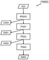
도 2는 이미지(예를 들어, 연속 투과 마스크 이미지, 바이너리 마스크 이미지, 곡선적 마스크 이미지 등)로부터 패터닝 디바이스 패턴(또는, 이후 마스크 패턴)을 결정하는 방법(P2000)의 흐름도이다. 곡선적 마스크 이미지는 주 또는 타겟 피처 및/또는 어시스트 피처(예를 들어, SRAF)를 포함하는 곡선적 또는 다각형 형상의 패턴들을 갖는 마스크(또는 마스크 패턴)의 이미지를 지칭한다. 마스크 패턴은 리소그래피 공정을 수반하는 패터닝 공정을 통해 기판 상에 프린트될 디자인 레이아웃 또는 타겟 패턴에 대응한다. 일 실시예에서, 디자인 레이아웃 또는 타겟 패턴은 바이너리 디자인 레이아웃, 연속톤 디자인 레이아웃, 또는 다른 적절한 형태의 디자인 레이아웃일 수 있다. 일 실시예에서, 타겟 패턴은 픽셀화된 이미지들로서 표현될 수 있다.2 is a flowchart of a method P2000 of determining a patterning device pattern (or hereinafter mask pattern) from an image (eg, a continuous transmission mask image, a binary mask image, a curved mask image, etc.). A curvilinear mask image refers to an image of a mask (or mask pattern) having curvilinear or polygonal shaped patterns including primary or target features and/or assist features (eg, SRAF). The mask pattern corresponds to a design layout or target pattern to be printed on a substrate through a patterning process involving a lithography process. In one embodiment, the design layout or target pattern may be a binary design layout, a contone design layout, or other suitable type of design layout. In one embodiment, the target pattern may be represented as pixelated images.
상기 방법은 반복 프로세스이며, 여기서 초기 연속톤 이미지(예를 들어, CTM 이미지)는 본 발명의 상이한 공정들에 따라 상이한 타입들의 이미지들을 생성하도록 점진적으로 수정되어, 결국 마스크를 제작/제조하는 데 사용될 수 있는 마스크 이미지(예를 들어, 곡선적 마스크 이미지)를 생성한다. 초기 연속톤 이미지(또는 일반적으로 초기 이미지라고 함)의 반복 수정은 비용 함수에 기초할 수 있으며, 여기서 매 반복 동안 초기 이미지는 비용 함수가 감소되도록(일 실시예에서, 최소화되도록) 수정될 수 있다. 일 실시예에서, 상기 방법은 기판 상의 시뮬레이션된 패턴의 윤곽들을 추적하고 CTM 이미지를 점진적으로 이진화하기 위해 리소-인지(litho-aware) 비용 함수[예를 들어, 에지 배치 오차(EPE)]를 이용한다. 전형적으로, CTM를 바이너리 이미지로 변환하는 프로세스는 부정확한 마스크 패턴을 유도하는 리소그래피 공정을 설명하지 않을 수 있는 계단 함수 및 마스크 패턴의 윤곽들(또는 경계)을 결정하기 위한 레벨-세트 방법(level-set method)을 수반할 수 있다.The method is an iterative process, wherein an initial contone image (eg, CTM image) is progressively modified to produce different types of images according to different processes of the present invention, eventually to be used to fabricate/manufacture the mask. Create a mask image that can be used (eg, a curved mask image). Iterative modification of the initial contone image (or generally referred to as the initial image) may be based on a cost function, wherein during each iteration the initial image may be modified such that the cost function is reduced (in one embodiment, minimized). . In one embodiment, the method uses a litho-aware cost function (e.g., edge placement error (EPE)) to trace the contours of a simulated pattern on a substrate and progressively binarize the CTM image. . Typically, the process of converting a CTM to a binary image is a level-set method for determining the contours (or boundaries) of a mask pattern and a step function that may not describe the lithographic process leading to an incorrect mask pattern. set method).
일 실시예에서, 프로세스 P201은 (ⅰ) 패터닝 공정을 거친 기판 상에 프린트될 타겟 패턴(201), (ⅱ) 타겟 패턴에 대응하는 패터닝 디바이스의 초기 이미지(202), (ⅲ) 초기 이미지를 변환하도록 구성되는 이진화 함수(203), 및 (ⅳ) 이진화 함수의 출력으로부터 기판 상의 패턴을 예측하도록 구성되는 공정 모델(204)을 얻는 것을 수반할 수 있다. 일 실시예에서, 상기 방법은 앞서 언급된 요소들 중 1 이상, 예를 들어 타겟 패턴(201) 및/또는 초기 이미지(202)를 생성하도록 수정될 수 있다.In one embodiment, process P201 includes (i) a
일 실시예에서, 타겟 패턴(201)은 바이너리 패턴, 연속톤 마스크 패턴, 또는 적절한 형태의 타겟 레이아웃일 수 있다. 타겟 패턴은 패터닝 공정을 거친 기판 상에 프린트될 것으로 예상되는 패턴이다. 타겟 이미지(201)에 대응하여, 초기 이미지(202)가 얻어질 수 있다. 초기 이미지(202)는 타겟 패턴(201)에 대응하는 OPC 관련 피처들(예를 들어, SRAF)을 포함하는 연속 투과 마스크 이미지일 수 있다.In one embodiment, the
일 실시예에서, 초기 이미지(202)는 기판 상에 프린트될 타겟 패턴에 기초하여 (예를 들어, 앞서 언급된 OPC 생성 프로세스를 포함한) 마스크 최적화 알고리즘에 의해 생성되는 CTM 이미지일 수 있다. 그 후, CTM 이미지는 프로세스 P201에 의해 수신될 수 있다. 일 실시예에서, 프로세스 P201은 CTM 이미지를 생성하도록 구성될 수 있다. 예를 들어, 예시적인 마스크 최적화 기술에서, 역 리소그래피 문제가 최적화 문제로서 공식화된다. 변수들은 마스크 이미지 내의 픽셀들의 값들과 관련될 수 있고, EPE 또는 사이드로브 프린팅과 같은 리소그래피 메트릭들이 비용 함수로서 사용될 수 있다. 최적화의 각각의 반복에서, 마스크 이미지가 변수들로부터 구성될 수 있고, 그 후 공정 모델(예를 들어, Tachyon 모델)이 적용되어 광학 또는 레지스트 이미지들을 얻고 비용 함수를 연산할 수 있다. 비용 함수 연산은 변수(예를 들어, 픽셀 세기)들을 업데이트하기 위해 최적화 솔버에서 사용되는 기울기 값들을 생성하는 기울기 연산을 수반한다. 최적화 동안 여러 번의 반복들 후에, 최종 마스크 이미지가 생성될 수 있으며, 이는 (예를 들어, Tachyon iOPC 및 SMO 소프트웨어에서 구현되는 바와 같이) 패턴 추출을 위한 안내 맵으로서 더 사용된다. 이러한 초기 이미지(예를 들어, CTM 이미지)는 패터닝 공정을 통해 기판 상에 프린트될 타겟 패턴에 대응하는 1 이상의 피처(예를 들어, 타겟 패턴의 피처, SRAF, 세리프 등)를 포함할 수 있다.In one embodiment, the
일 실시예에서, 이진화 함수(203)는 초기 이미지를 바이너리 이미지로 점진적으로 변환하도록 구성될 수 있다. 일 실시예에서, 이진화 함수는 다음 형태의 로지스틱 함수일 수 있다:In one embodiment, the

앞선 수학식에서, L은 곡선의 최대값이고, k는 곡선의 경사도이며, φ0은 곡선의 중점에서의 변수 φ의 값이다. 일 실시예에서, 변수 φ는 레벨-세트 함수 또는 이미지 내의 픽셀 위치들일 수 있다. 일 실시예에서, 로지스틱 함수는 시그모이드 함수(즉, 이때 k=1, φ0=0, 및 L=1), 아크탄젠트(즉, 역 탄젠트) 함수, 및/또는 다음과 같은 형태의 계단 함수일 수 있다(수학식 2):In the preceding equation, L is the maximum value of the curve, k is the slope of the curve, and φ0 is the value of the variable φ at the midpoint of the curve. In one embodiment, the variable φ may be a level-set function or pixel locations within the image. In one embodiment, the logistic function is a sigmoid function (ie, where k=1, φ0 =0, and L=1), an arctangent (ie, inverse tangent) function, and/or a step of the form It can be a function (Equation 2):

또 다른 실시예에서, 이진화 함수는 다음과 같은 기본 로지스틱 함수에 기초한 함수들의 세트일 수 있다:In another embodiment, the binarization function may be a set of functions based on a basic logistic function as follows:


앞선 수학식 3 내지 수학식 7의 세트에서, 변수 φ는 레벨-세트 함수 또는 이미지 내의 픽셀 위치들일 수 있고, f(φ)는 마스크 이미지를 나타내며, low는 함수 f의 최저값이고, high는 함수 f의 최고값이며, k는 곡선의 경사도이고, threshold는 고정된 컷오프가 아니라 점진적 컷오프 또는 소프트 에지가 존재하도록 선택된 값 또는 함수일 수 있다. 일 실시예에서, k 및 threshold는 최적화 프로세스 동안 점진적 이진화를 위해 설정/수정될 수 있다. 일 실시예에서, k 및 threshold는 본 방법에 따른 최적화 프로세스 동안 업데이트될 수 있는 튜닝 파라미터들일 수 있다. 수학식 3 내지 수학식 7의 함수들의 예시적인 튜닝이 도 3에 예시되며, 여기서 파라미터 k(즉, 곡선의 경사도)는 비용 함수에 기초하여 점진적으로 변화(예를 들어, k=1에서 k=20까지 증가)된다. 따라서, 이진 함수는 초기 CTM 이미지를 이진화된 이미지로 점진적으로 변환하며, 아래의 프로세스들에서 더 논의된다. 결과적인 바이너리 이미지는 곡선적 마스크를 제조하는 데 더 사용될 수 있다.In the set of Equations 3 to 7 above, the variable φ may be a level-set function or pixel positions in an image, f(φ) represents the mask image, low is the lowest value of the function f, and high is the function f is the highest value of , k is the slope of the curve, and the threshold may be a value or function chosen such that there is a gradual cutoff or soft edge rather than a fixed cutoff. In one embodiment, k and threshold may be set/modified for progressive binarization during the optimization process. In one embodiment, k and threshold may be tuning parameters that may be updated during the optimization process according to the present method. An exemplary tuning of the functions of Equations 3-7 is illustrated in FIG. 3 , where the parameter k (ie, the slope of the curve) gradually changes based on a cost function (eg, from k=1 to k= increased to 20). Thus, the binary function progressively transforms the initial CTM image into a binarized image, which is further discussed in the processes below. The resulting binary image can be further used to fabricate a curvilinear mask.
일 실시예에서, 공정 모델(204)은 이진화 함수의 출력으로부터 기판 상의 패턴을 예측하도록 구성될 수 있다. 일 실시예에서, 공정 모델은 M3D 모델, 광학 모델, 레지스트 모델, 에칭 모델 등 중 1 이상일 수 있으며, 이들은 서로 연결되어 한 모델로부터 입력들을 수신하고(예를 들어, 광학 모델이 M3D 모델로부터 입력을 수신함), 또 다른 연결된 모델로 출력을 송신할 수 있다(예를 들어, 광학 모델은 레지스트 모델로 출력을 송신함). 일 실시예에서, 공정 모델들은 당업자에게 알려질 수 있는 바와 같이, 물리-기반 모델, 경험적 모델, 및/또는 기계 학습-기반 모델일 수 있다.In one embodiment, the
또한, 상기 방법은 비용 함수에 기초하여 반(semi)-이진화 및/또는 이진화 이미지(예를 들어, 2002)를 생성하기 위해 초기 이미지(예를 들어, 201)를 반복적으로 업데이트함으로써 초기 이미지에 대응하는 마스크 패턴을 갖는 이진화된 이미지를 생성하는 프로세스 P203를 수반할 수 있다. 각각의 반복에서, 비용 함수는 (예를 들어, 프로세스 P207, P209, P211, 및 P213에서) 추후 논의되는 바와 같이 점진적으로 감소된다. 반-이진화 및/또는 이진화 또는 변환된 이미지(2002)는 초기 이미지에 이진화 함수(예를 들어, 수학식 1 내지 수학식 7 중 1 이상)를 적용함으로써 생성될 수 있다. 프로세스 P203의 끝에서, 초기 이미지(201)는 중간 이미지(2002)에 점진적으로 관여하여, 결국 최종 바이너리 이미지(2003), 예를 들어 도 3의 이미지(306)를 유도한다.Further, the method corresponds to the initial image by iteratively updating the initial image (eg, 201) to generate a semi-binarized and/or binarized image (eg, 2002) based on the cost function. process P203 of generating a binarized image having a mask pattern that At each iteration, the cost function is progressively reduced (eg, in processes P207, P209, P211, and P213) as discussed below. The semi-binarized and/or binarized or transformed
도 3에서, 예시적인 타겟 이미지(301)는 기판의 중심에서의 접촉홀을 포함할 수 있다. 타겟 이미지(301)는 CTM 이미지(302)를 얻는/생성하는 데 사용될 수 있으며, 이는 이진화 함수를 적용함으로써 반-이진화 및/또는 이진화된 이미지(304)로 더 변환될 수 있는 초기 이미지(201)의 일 예시일 수 있다. 비용 함수에 기초한 최적화 프로세스의 여러 번의 반복 후에, 초기 이미지(302)는 최종 이진화된 이미지(306)로 점진적으로 진화할 수 있다. 또한, 일 실시예에서, 최종 이진화된 이미지(306)의 복수의 짧은 세그먼트들이 더 긴 세그먼트, 계단 패턴(stair step pattern), 대각선, 대각선 세그먼트와 조합된 수평 또는 수직 세그먼트, 또는 이들의 조합으로 대체될 수 있다. 예를 들어, 최종 이진화된 이미지(306) 내의 패턴들이 계단식 이미지(staircase image: 308)에 나타낸 바와 같이 계단 패턴들로 전환될 수 있다. 이미지들(304 및 306)에서, CTM 이미지(302)에 도시된 곡선적 패턴들(예를 들어, 접촉홀 및 접촉홀 주위의 SRAF)이 보존되는 것으로 관찰될 수 있다.In FIG. 3 , an
일 실시예에서, (예를 들어, 수학식 1 내지 수학식 6을 사용하여) 이진화를 가능하게 하기 위해, 임계값이 (예를 들어, 수학식 5 또는 수학식 6에 나타낸 바와 같이) 로지스틱 함수 기반 변환의 결과에 할당될 수 있다. 예를 들어, 최대값 및 최소값 "1" 및 "0"을 각각 갖는 시그모이드 함수의 경우, 임계값은 대략 0.5(또는 0.5 미만)일 수 있으며, 이는 시그모이드 변환 후에 대략 0.5보다 큰 값을 갖는 결과적인 이미지의 픽셀에 값 1이 할당될 수 있고, 0.5보다 낮은 경우에는 값 0이 할당될 수 있음을 나타낸다. 일 실시예에서, 계단 함수가 사용되는 경우, 바이너리 "1"은 임계값보다 큰 값들을 갖는 픽셀에 할당될 수 있고, 바이너리 "0"은 임계값보다 작은 값들을 갖는 픽셀에 할당될 수 있다. 계단 함수는 임계치에서 불연속이지만, 마스크 변수들에 대한 마스크 이미지의 기울기의 정확한 수학적 형태가 예를 들어 다음과 같이 전개될 수 있다:In one embodiment, to enable binarization (e.g., using Equations 1-6), the threshold is a logistic function (e.g., as shown in Equation 5 or Equation 6) It can be assigned to the result of the base transformation. For example, for a sigmoid function with maximum and minimum values "1" and "0", respectively, the threshold may be approximately 0.5 (or less than 0.5), which after sigmoid transformation is greater than approximately 0.5. indicates that a pixel in the resulting image with . In one embodiment, when a step function is used, a binary “1” may be assigned to pixels with values greater than a threshold, and a binary “0” may be assigned to pixels with values less than a threshold. The step function is discrete at the threshold, but the exact mathematical form of the slope of the mask image with respect to the mask parameters can be developed, for example:

앞선 수학식에서, MI는 마스크 변수들 Φ에 계단 함수를 적용함으로써 얻어진 마스크 이미지를 나타내고, w는 변수들 Φ를 업샘플링/다운샘플링하는 데 사용되는 엘리어싱-제거 윈도우 함수(anti-aliasing window function)이다. 따라서, 이진화 함수는 시그모이드/아크탄젠트, 또는 계단 함수 또는 둘 모두일 수 있다. 또한, 마스크 변수들에 대한 비용 함수의 기울기가 전개된다. 일 실시예에서, 비용 함수의 기울기를 결정하는 단계는 시그모이드 함수, 아크탄젠트 함수, 및 계단 함수 중 적어도 하나(또는 전부)를 포함하는 이진화 함수에 대해 마스크 변수들에 대한 완전한 기울기를 연산하는 단계를 수반한다.In the preceding equation, MI denotes a mask image obtained by applying a step function to mask variables Φ, and w denotes an anti-aliasing window function used for upsampling/downsampling variables Φ. to be. Thus, the binarization function can be a sigmoid/arctangent, or a step function, or both. Also, the slope of the cost function for the mask variables is developed. In one embodiment, determining the slope of the cost function comprises calculating the complete slope for the mask variables for a binarization function comprising at least one (or all) of a sigmoid function, an arctangent function, and a step function. It involves steps.
일 실시예에서, 이진화는 EPE 기반 비용 함수 및/또는 MSE, MXE, RMS 등과 같은 여하한의 다른 비용 함수(또는 목적 함수) 메트릭과 함께 사용될 수 있다. 일 실시예에서, 이진화는 정규 MSE/MXE 비용 함수를 사용하여 예측된 패턴을 더 개선하기 위해 미세 튜닝 프로세스로서 정규 MSE/MXE 비용 함수와 함께 사용될 수 있다. 예를 들어, 프로세스들 P207, P211, 및 P213에 대해 논의된 바와 같다.In one embodiment, binarization may be used with an EPE based cost function and/or any other cost function (or objective function) metric such as MSE, MXE, RMS, etc. In one embodiment, binarization can be used with the canonical MSE/MXE cost function as a fine-tuning process to further refine the pattern predicted using the canonical MSE/MXE cost function. For example, as discussed for processes P207, P211, and P213.
반-이진화/이진화된(또는 변환된) 이미지(2002)를 생성한 후에, 프로세스 P205는 공정 모델의 시뮬레이션을 통해 이미지(2002)에 기초하여 기판 상에 형성될 수 있는 예측된 패턴(2005)을 예측하는 단계를 수반할 수 있다. 앞서 논의된 바와 같이, 공정 모델은 함께 연결될 수 있는 M3D 모델, 광학 모델, 레지스트 모델 등 중 1 이상일 수 있다. 일 실시예에서, 공정 모델은 물리-기반 모델, 경험적 모델, 및/또는 기계 학습-기반 모델일 수 있다.After generating the semi-binarized/binarized (or transformed)
또한, 상기 방법은 프로세스 P207에서, 예측된 패턴(2005)으로부터 윤곽들을 추출하는 단계 및 비용 함수를 평가하는 단계를 수반할 수 있다. 비용 함수는 에지 배치 오차, 결함 기반 메트릭, 및/또는 MRC 위반 확률과 같은 마스크 규칙 체크 기반 메트릭일 수 있다.The method may also involve, in process P207 , extracting contours from the predicted
일 실시예에서, 비용 함수는 본 발명에 따른 에지 포인트 향상 기술을 사용할 수 있다. 에지 포인트 향상 기술에서는, 윤곽이 예측된 패턴 및 타겟 패턴의 1 이상의 주 피처 및/또는 1 이상의 광 근접 보정의 에지에 피팅된다. 즉, 윤곽은 1 이상의 주 피처 및/또는 1 이상의 광 근접 보정의 에지 포인트들에 피팅되거나 이를 추적한다. 일 실시예에서, 에지 포인트 향상 기술은 여하한의 윤곽 식별 기술을 사용하여 예측된 패턴 및/또는 타겟 패턴의 이미지(예를 들어, 그레이-스케일 이미지)를 1 이상의 주 피처 및/또는 1 이상의 광 근접 보정의 윤곽들(예를 들어, GDSII, OASIS 또는 다른 포맷)로 전환하는 것을 수반한다. 예를 들어, 윤곽 식별 기술은 에지를 식별하고 임계치를 적용하여 윤곽을 식별하는 것(예를 들어, 에지에 수직이고 에지를 통해 진행하는 라인들을 따라 그레이-스케일 값들을 평가하여, 그레이-스케일 값이 소정 임계치를 지나는 곳을 식별하고 이를 윤곽 위치로서 식별하는 것)을 수반할 수 있다. 일 실시예에서, 윤곽 식별 기술은 윤곽을 추출하기 위해 에지를 따른 지점들에서의 기울기를 평가할 수 있다. 일 실시예에서, 이미지는 윤곽 식별을 위해 더 미세한 픽셀 그리드로 업스케일링될 수 있다. 일 실시예에서, 이미지는 바이너리 픽셀, 예를 들어 본 명세서에 설명된 바와 같은 기술을 사용하여 얻어지는 이진화된 버전을 가질 수 있다. 일 실시예에서, 1 이상의 윤곽은 예측된 패턴 및 타겟 패턴의 이미지 데이터로부터 추출되고, 목적 함수 평가에 사용된다.In one embodiment, the cost function may use an edge point enhancement technique according to the present invention. In the edge point enhancement technique, a contour is fitted to one or more major features of the predicted pattern and target pattern and/or one or more edges of optical proximity correction. That is, the contour fits or tracks one or more main features and/or one or more optical proximity correction edge points. In one embodiment, the edge point enhancement technique uses any contour identification technique to convert an image (eg, a gray-scale image) of the predicted pattern and/or target pattern to one or more main features and/or one or more lights. It involves converting to contours of proximity correction (eg GDSII, OASIS or other format). For example, a contour identification technique identifies an edge and applies a threshold to identify a contour (e.g., evaluating gray-scale values along lines that are perpendicular to the edge and running through the edge, so that the gray-scale value identifying where this predetermined threshold is crossed and identifying it as a contour location). In one embodiment, the contour identification technique may evaluate the slope at points along the edge to extract the contour. In one embodiment, the image may be upscaled to a finer pixel grid for contour identification. In one embodiment, the image may have binary pixels, eg, a binarized version obtained using techniques as described herein. In one embodiment, one or more contours are extracted from image data of the predicted pattern and the target pattern and used for objective function evaluation.
일 실시예에서, 예측된 패턴 및 타겟 패턴의 처리는 이미지(또는 이미지 데이터)에서 타겟 패턴에 대응하는 피처들 각각의 에지를 식별하는 것을 수반할 수 있다. 또한, 일 실시예에서, 더 높은 중요도(예를 들어, 가중치)가 또 다른 부분, 예를 들어 디자인 패턴의 광 근접 보정(들) 및/또는 다른 부분들보다는 이미지 내의 예측된 및/또는 타겟 피처들의 1 이상의 식별된 에지들에 할당될 수 있다.In one embodiment, processing the predicted pattern and the target pattern may involve identifying an edge of each of the features corresponding to the target pattern in the image (or image data). Further, in one embodiment, a higher importance (eg, weight) is a predicted and/or target feature in the image rather than another portion, eg, optical proximity correction(s) and/or other portions of the design pattern. may be assigned to one or more identified edges of
또한, 상기 방법은 프로세스 P209에서, 비용 함수가 감소되는지(일 실시예에서, 최소화되는지)를 결정하는 단계를 수반할 수 있다.The method may also involve, in process P209, determining whether the cost function is reduced (in one embodiment, minimized).
일 실시예에서, 비용 함수가 최소화되지 않은 경우, 상기 방법은 프로세스 P211에서 비용 함수의 기울기[또는 기울기 맵(2011)]를 결정하는 단계를 수반할 수 있다. 일 실시예에서, 프로세스 P211는 비용 함수(예를 들어, EPE)에 기초하여 기울기 맵(2011)을 생성하는 단계를 수반할 수 있다. 기울기 맵(2011)은 비용 함수의 도함수 및/또는 편도함수일 수 있다. 일 실시예에서, 비용 함수의 편도함수는 마스크 이미지의 변수들에 대해 결정될 수 있고, 도함수는 이진화 함수 및/또는 초기 이미지(201)의 변수들에 대한 편도함수를 결정하기 위해 더 연결(chain)될 수 있다.In one embodiment, if the cost function is not minimized, the method may involve determining a slope (or slope map 2011 ) of the cost function in process P211 . In one embodiment, process P211 may involve generating a
기울기 맵(2011)은 비용 함수의 값이 감소되는, 일 실시예에서는 최소화되는 방식으로 마스크 변수들의 값들(즉, 초기 이미지 또는 이진화 함수의 값들)의 증가 또는 감소에 대한 권고를 제공할 수 있다. 일 실시예에서, 최적화 알고리즘이 마스크 변수 값들을 결정하기 위해 기울기 맵(2011)에 적용될 수 있다. 일 실시예에서, 최적화 솔버 켤레 기울기 또는 준-뉴턴 방법이 기울기-기반 연산을 수행하기 위해 사용될 수 있다.
또한, 상기 방법은 프로세스 P213에서, 비용 함수가 점진적으로 감소되도록(일 실시예에서, 최소화되도록) 비용 함수의 기울기 맵(2011)에 기초하여 초기 이미지에 대응하는 마스크 변수들의 값들[예를 들어, 초기 이미지(201) 내의 픽셀들의 세기들] 및/또는 이진화 함수의 파라미터들(예를 들어, 수학식 1 내지 수학식 6에서의 k 및 임계치)을 결정하고 수정하는 단계를 수반할 수 있다. 그 후, 상기 방법은 프로세스 P203로 되돌아가고 루프에서 후속 프로세스들(즉, P205, P207, P209, P211 및 P213)을 수행할 수 있다. 여러 번의 반복 끝에(예를 들어, 비용 함수가 최소화되는 경우), 얻어지는 이진화된 이미지는 CTM 이미지들과 유사한 곡선적 패턴들을 포함한다. 따라서, 각각의 반복에서, 초기 이미지(201)는 패터닝 공정의 효과들이 고려되도록 이진화된 이미지(2003)로 변환된다. 예를 들어, 각각의 반복에서, 패터닝 공정의 효과들(및 연계된 변동)은 공정 모델의 시뮬레이션, 공정 모델의 출력에 기초하는 비용 함수(예를 들어, EPE) 및 비용 함수에 기초하는 기울기 맵을 통해 설명된다.The method also includes, in process P213, values of mask variables corresponding to the initial image based on the
일 실시예에서, 마스크 패턴(또는 마스크 이미지)의 정규화 프로세스가 수행될 수 있다. 정규화 프로세스는, 예를 들어 CTM 이미지들로부터 생성될 수 있고 결과적으로 이러한 CTM 이미지들로부터 생성되는 이진화된 마스크 이미지에 나타날 수 있는 복잡한 마스크 패턴들을 단순화한다. 일 실시예에서, ILT 솔루션 공간이 규정되지 않은 경우, 이는 ILT 솔루션의 값을 심하게 손상시키는 MRC를 위반하는 복잡한 마스크 패턴들을 생성할 수 있다. 이러한 문제를 해결하기 위해, 마스크 이미지를 "맨해튼" 형상 또는 "곡선" 형상으로 정규화하는 방법이 EPE 기반 비용 함수와 함께 수행될 수 있다. 정규화 프로세스는 마스크 복잡도를 감소시키기 위해 바람직한 형상들로 진화하도록 마스크 이미지를 안내한다. 예를 들어, 정규화 프로세스는 비용 함수 측면(예를 들어, MRC 위반 확률)으로서 앞선 방법에 통합될 수 있고, 앞서 논의된 EPE-기반 기울기 연산과 유사한 방식으로 기울기 연산에 더 통합될 수 있다.In one embodiment, a normalization process of the mask pattern (or mask image) may be performed. The normalization process simplifies complex mask patterns that may be generated from, for example, CTM images and consequently appear in a binarized mask image generated from such CTM images. In one embodiment, if the ILT solution space is not defined, this can create complex mask patterns that violate MRC which severely impairs the value of the ILT solution. To solve this problem, a method of normalizing the mask image to a “Manhattan” shape or a “curve” shape can be performed with an EPE-based cost function. The normalization process guides the mask image to evolve into desirable shapes to reduce mask complexity. For example, the normalization process may be incorporated into the preceding method as a cost function aspect (eg, MRC violation probability), and may be further incorporated into the gradient operation in a manner similar to the EPE-based gradient operation discussed above.
도 5는 MRC를 충족하는 계단 마스크 및 마스크 패턴을 생성하기 위해 도 2의 프로세스(P2000)를 더 적용하는 방법(P5000)의 흐름도이다. 상기 방법(P5000)은 앞서 논의된 바와 같이 초기 이미지(202)(예를 들어, CTM 이미지)를 수신하거나 얻을 시에 시작한다. 일 실시예에서, 상기 방법(P5000)은 프로세스 P2000로부터 얻어진 이진화된 마스크 패턴(2003)을 더 수정하거나 업데이트하기 위해 여하한의 다른 마스크 최적화 프로세스에서 사용될 수 있다.5 is a flow diagram of a method P5000 of further applying the process P2000 of FIG. 2 to generate a step mask and mask pattern that meets the MRC. The method P5000 begins upon receiving or obtaining an initial image 202 (eg, a CTM image) as discussed above. In one embodiment, the method P5000 may be used in any other mask optimization process to further modify or update the
프로세스 P2000에서, 초기 이미지(202)는 앞서 논의된 바와 같이 점진적으로 이진화된다. 일 실시예에서, 시그모이드 함수가 프로세스 P2000에서 사용될 수 있으며, 이는 "0" 또는 "1" 사이 또는 대략 "0" 또는 "1"에 근접한 픽셀 값들을 갖는 이진화된 이미지(2003)를 생성할 수 있다(예를 들어, 픽셀은 0.9보다 크고 0.1보다 작은 값들을 가질 수 있음). 이러한 이진화된 이미지(2003)가 프로세스 P501에서 계단 함수를 적용함으로써 곡선적 마스크 이미지(5001)로 더 변환될 수 있다. 계단 함수는 이진화된 이미지(2003)의 픽셀들을 "0" 또는 "1"의 값을 갖는 픽셀들로 변환한다. 일 실시예에서, 계단 함수는 마스크 변수들을 픽셀 값들 "0" 또는 "1"을 갖는 이진화된 이미지로 변환하기 위해 직접 사용될 수 있다.In process P2000, the
또한, 프로세스 P503에서, 곡선적 마스크 이미지(5001)는 앞서 논의된 바와 같이 계단 패턴을 갖는 계단식 이미지(5003)로 변환될 수 있다. 일 실시예에서, 곡선적 윤곽(또는 패턴)을 계단 패턴으로 변환하기 위해, 먼저 중단 지점(breaking point)들이 곡선적 윤곽 상에서 식별된다. 둘째로, 곡선적 윤곽은 중단 지점들을 사용하여 로프(또는 바아 형상)들로 쪼개지고, 로프 끝점에 대한 방향들이 연산된다. 마지막으로, 중단 지점들은 계단식 다각형들을 얻기 위해 수평 및 수직 라인들로 연결된다.Also, in process P503, the
또한, 프로세스 P505에서, MRC 위반들이 이미지(5001 및/또는 5003)에 대해 결정될 수 있다. 마스크 규칙 체크는 마스크의 제조가능성에 기초한 규칙들 또는 체크들의 세트로서 정의될 수 있고, 이러한 마스크 규칙 체크들은 마스크 패턴(예를 들어, OPC를 포함한 곡선적 패턴)이 제조될 수 있는지 여부를 결정하기 위해 평가될 수 있다. 일 실시예에서, MRC는 [예를 들어, 이프-덴-엘스(if-then-else) 조건 체크들을 포함한] 알고리즘의 형태로 구현될 수 있다. 예를 들어, 마스크 규칙 체크는 CD 값들, 두 피처 사이(예를 들어, 타겟 피처 대 SRAF 또는 SRAF 대 SRAF)의 거리, 피처의 곡률 반경, 또는 다른 기하학적 파라미터에 기초할 수 있다. 일 실시예에서, 앞서 논의된 바와 같이, 프로세스 P505는 이진화 프로세스의 일부일 수 있으며, 여기서 비용 함수는 MRC 위반들의 수, MRC 위반 또는 MRC 위반이 없음을 나타내는 바이너리 변수, MRC 위반 확률, 또는 다른 적절한 MRC 관련 메트릭과 같은 MRC 메트릭을 포함할 수 있다.Also, in process P505 , MRC violations may be determined for
일 실시예에서, 곡선적 패턴들을 갖는 이진화된 마스크 이미지(2003), 계단 패턴(5001)을 갖는 계단식 마스크 이미지(5003), 및/또는 (MRC를 설명하는) 마스크 이미지(5005)는 패터닝 디바이스로 제조 또는 제작될 수 있다. 이러한 패터닝 디바이스는 이미지들(2003, 5001, 및/또는 5005)에 대응하는 구조적 피처들(예를 들어, 타겟 패턴, OPC 등)을 포함할 것이다. 또한, 패터닝 디바이스는 기판 상에 대응하는 패턴(예를 들어, 타겟 패턴)을 프린트하기 위해 패터닝 단계 동안 패터닝 장치(예를 들어, 리소그래피 장치 또는 스캐너)에 의해 사용될 수 있다.In one embodiment, the
본 발명에 따른 방법은 소스 마스크 최적화, 마스크 최적화, 및/또는 OPC를 포함하는 마스크 최적화 프로세스의 상이한 측면들에 포함될 수 있고, 적절한 곡선적 마스크 패턴이 결정될 수 있다.A method according to the present invention may be included in different aspects of a mask optimization process including source mask optimization, mask optimization, and/or OPC, and an appropriate curvilinear mask pattern may be determined.
도 6은 본 명세서에 개시된 방법들, 흐름들 및 장치를 구현하는 데 도움이 될 수 있는 컴퓨터 시스템(100)을 나타내는 블록 다이어그램이다. 컴퓨터 시스템(100)은 정보를 전달하는 버스(102) 또는 다른 통신 기구, 및 정보를 처리하는 버스(102)와 커플링된 프로세서(104)[또는 다중 프로세서들(104 및 105)]를 포함한다. 또한, 컴퓨터 시스템(100)은 프로세서(104)에 의해 실행될 정보 및 명령어들을 저장하는 RAM(random access memory) 또는 다른 동적 저장 디바이스와 같은, 버스(102)에 커플링된 주 메모리(106)를 포함한다. 또한, 주 메모리(106)는 프로세서(104)에 의해 실행될 명령어들의 실행 시 임시 변수들 또는 다른 매개 정보(intermediate information)를 저장하는 데 사용될 수 있다. 컴퓨터 시스템(100)은 프로세서(104)에 대한 정적 정보 및 명령어들을 저장하는 버스(102)에 커플링된 ROM(read only memory: 108) 또는 다른 정적 저장 디바이스를 더 포함한다. 자기 디스크 또는 광학 디스크와 같은 저장 디바이스(110)가 제공되고 버스(102)에 커플링되어 정보 및 명령어들을 저장한다.6 is a block diagram illustrating a
컴퓨터 시스템(100)은 버스(102)를 통해, 컴퓨터 사용자에게 정보를 보여주는 CRT(cathode ray tube) 또는 평판 또는 터치 패널 디스플레이(touch panel display)와 같은 디스플레이(112)에 커플링될 수 있다. 영숫자 및 다른 키들을 포함한 입력 디바이스(114)는 정보 및 명령 선택(command selection)들을 프로세서(104)로 전달하기 위해 버스(102)에 커플링된다. 또 다른 타입의 사용자 입력 디바이스는 방향 정보 및 명령 선택들을 프로세서(104)로 전달하고, 디스플레이(112) 상의 커서 움직임을 제어하기 위한 마우스, 트랙볼(trackball) 또는 커서 방향키들과 같은 커서 제어부(cursor control: 116)이다. 이 입력 디바이스는, 통상적으로 디바이스로 하여금 평면에서의 위치들을 특정하게 하는 2 개의 축선인 제 1 축선(예를 들어, x) 및 제 2 축선(예를 들어, y)에서 2 자유도를 갖는다. 또한, 입력 디바이스로서 터치 패널(스크린) 디스플레이가 사용될 수도 있다.
일 실시예에 따르면, 주 메모리(106)에 포함된 1 이상의 명령어들의 1 이상의 시퀀스를 실행하는 프로세서(104)에 응답하여 컴퓨터 시스템(100)에 의해 본 명세서에 설명된 1 이상의 방법의 부분들이 수행될 수 있다. 이러한 명령어들은 저장 디바이스(110)와 같은 또 다른 컴퓨터-판독가능한 매체로부터 주 메모리(106)로 읽혀질 수 있다. 주 메모리(106) 내에 포함된 명령어들의 시퀀스들의 실행은, 프로세서(104)가 본 명세서에 설명된 공정 단계들을 수행하게 한다. 또한, 주 메모리(106) 내에 포함된 명령어들의 시퀀스들을 실행하기 위해 다중 처리 구성(multi-processing arrangement)의 1 이상의 프로세서가 채택될 수 있다. 대안적인 실시예에서, 하드웨어에 내장된 회로(hard-wired circuitry)가 소프트웨어 명령어들과 조합하거나 그를 대신하여 사용될 수 있다. 따라서, 본 명세서의 기재내용은 하드웨어 회로와 소프트웨어의 여하한의 특정 조합에 제한되지 않는다.According to one embodiment, portions of one or more methods described herein are performed by the
본 명세서에서 사용된 "컴퓨터-판독가능한 매체"라는 용어는 실행을 위해 프로세서(104)에 명령어를 제공하는 데 관여하는 여하한의 매체를 칭한다. 이러한 매체는 비휘발성 매체(non-volatile media), 휘발성 매체 및 전송 매체를 포함하는 다수의 형태를 취할 수 있으며, 이에 제한되지는 않는다. 비휘발성 매체는, 예를 들어 저장 디바이스(110)와 같은 광학 또는 자기 디스크를 포함한다. 휘발성 매체는 주 메모리(106)와 같은 동적 메모리를 포함한다. 전송 매체는 버스(102)를 포함하는 와이어들을 포함하여, 동축 케이블(coaxial cable), 구리선 및 광섬유를 포함한다. 또한, 전송 매체는 무선 주파수(RF) 및 적외선(IR) 데이터 통신 시 발생되는 파장들과 같이 음파(acoustic wave) 또는 광파의 형태를 취할 수도 있다. 컴퓨터-판독가능한 매체의 보편적인 형태들은, 예를 들어 플로피 디스크(floppy disk), 플렉시블 디스크(flexible disk), 하드 디스크, 자기 테이프, 여하한의 다른 자기 매체, CD-ROM, DVD, 여하한의 다른 광학 매체, 펀치 카드(punch card), 종이 테이프(paper tape), 홀(hole)들의 패턴을 갖는 여하한의 다른 물리적 매체, RAM, PROM, 및 EPROM, FLASH-EPROM, 여하한의 다른 메모리 칩 또는 카트리지(cartridge), 이후 설명되는 바와 같은 반송파, 또는 컴퓨터가 판독할 수 있는 여하한의 다른 매체를 포함한다.The term “computer-readable medium” as used herein refers to any medium that participates in providing instructions to the
다양한 형태의 컴퓨터 판독가능한 매체는 실행을 위해 1 이상의 명령어들의 1 이상의 시퀀스를 프로세서(104)로 전달하는 데 관련될 수 있다. 예를 들어, 명령어들은 초기에 원격 컴퓨터의 자기 디스크 상에 저장되어 있을 수 있다(bear). 원격 컴퓨터는 그 동적 메모리로 명령어들을 로딩하고, 모뎀을 이용하여 전화선을 통해 명령어들을 보낼 수 있다. 컴퓨터 시스템(100)에 로컬인 모뎀이 전화선 상의 데이터를 수신하고, 상기 데이터를 적외선 신호로 전환하기 위해 적외선 송신기를 사용할 수 있다. 버스(102)에 커플링된 적외선 검출기는 적외선 신호로 전달된 데이터를 수신하고, 상기 데이터를 버스(102)에 놓을 수 있다. 버스(102)는, 프로세서(104)가 명령어들을 회수하고 실행하는 주 메모리(106)로 상기 데이터를 전달한다. 주 메모리(106)에 의해 수신된 명령어들은 프로세서(104)에 의한 실행 전이나 후에 저장 디바이스(110)에 선택적으로 저장될 수 있다.Various forms of computer readable media may be involved in carrying one or more sequences of one or more instructions to the
또한, 컴퓨터 시스템(100)은 버스(102)에 커플링된 통신 인터페이스(118)를 포함할 수 있다. 통신 인터페이스(118)는 로컬 네트워크(122)에 연결되는 네트워크 링크(120)에 커플링하여 양방향(two-way) 데이터 통신을 제공한다. 예를 들어, 통신 인터페이스(118)는 ISDN(integrated services digital network) 카드 또는 대응하는 타입의 전화선에 데이터 통신 연결을 제공하는 모뎀일 수 있다. 또 다른 예시로서, 통신 인터페이스(118)는 호환성 LAN에 데이터 통신 연결을 제공하는 LAN(local area network) 카드일 수 있다. 또한, 무선 링크가 구현될 수도 있다. 여하한의 이러한 구현에서, 통신 인터페이스(118)는 다양한 타입의 정보를 나타내는 디지털 데이터 스트림들을 전달하는 전기적, 전자기적 또는 광학적 신호들을 송신하고 수신한다.
통상적으로, 네트워크 링크(120)는 1 이상의 네트워크를 통해 다른 데이터 디바이스에 데이터 통신을 제공한다. 예를 들어, 네트워크 링크(120)는 로컬 네트워크(122)를 통해 호스트 컴퓨터(host computer: 124), 또는 ISP(Internet Service Provider: 126)에 의해 작동되는 데이터 장비로의 연결을 제공할 수 있다. 차례로, ISP(126)는 이제 보편적으로 "인터넷"(128)이라고 칭하는 월드와이드 패킷 데이터 통신 네트워크를 통해 데이터 통신 서비스를 제공한다. 로컬 네트워크(122) 및 인터넷(128)은 둘 다 디지털 데이터 스트림들을 전달하는 전기적, 전자기적 또는 광학적 신호들을 사용한다. 다양한 네트워크를 통한 신호들, 및 컴퓨터 시스템(100)에 또한 그로부터 디지털 데이터를 전달하는 통신 인터페이스(118)를 통한 네트워크 링크(120) 상의 신호들은 정보를 전달하는 반송파의 예시적인 형태들이다.Typically,
컴퓨터 시스템(100)은 네트워크(들), 네트워크 링크(120) 및 통신 인터페이스(118)를 통해 메시지들을 송신하고, 프로그램 코드를 포함한 데이터를 수신할 수 있다. 인터넷 예시에서는, 서버(130)가 인터넷(128), ISP(126), 로컬 네트워크(122) 및 통신 인터페이스(118)를 통해 어플리케이션 프로그램에 대한 요청된 코드를 전송할 수 있다. 하나의 이러한 다운로드된 어플리케이션은, 예를 들어 본 명세서에 설명된 방법의 일부 또는 전부를 제공할 수 있다. 수신된 코드는 수신될 때 프로세서(104)에 의해 실행될 수 있고, 및/또는 추후 실행을 위해 저장 디바이스(110) 또는 다른 비휘발성 저장소에 저장될 수 있다. 이 방식으로, 컴퓨터 시스템(100)은 반송파의 형태로 어플리케이션 코드를 얻을 수 있다.
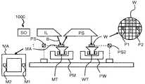
도 7은 본 명세서에 설명된 기술들이 이용될 수 있는 예시적인 리소그래피 투영 장치를 개략적으로 도시한다. 상기 장치는:7 schematically illustrates an exemplary lithographic projection apparatus in which the techniques described herein may be employed. The device is:
- 방사선 빔(B)을 컨디셔닝(condition)하는 조명 시스템(IL) -이러한 특정한 경우, 조명 시스템은 방사선 소스(SO)도 포함함- ;- an illumination system IL, which conditions the radiation beam B, which in this particular case also comprises a radiation source SO;
- 패터닝 디바이스(MA)(예를 들어, 레티클)를 유지하는 패터닝 디바이스 홀더가 제공되고, 아이템(PS)에 대하여 패터닝 디바이스를 정확히 위치시키는 제 1 위치설정기에 연결되는 제 1 대상물 테이블(예를 들어, 패터닝 디바이스 테이블)(MT);- a first object table (for example) provided with a patterning device holder for holding the patterning device MA (for example a reticle) and connected to a first positioner for accurately positioning the patterning device with respect to the item PS , patterning device table) (MT);
- 기판(W)(예를 들어, 레지스트-코팅된 실리콘 웨이퍼)을 유지하는 기판 홀더가 제공되고, 아이템(PS)에 대하여 기판을 정확히 위치시키는 제 2 위치설정기에 연결되는 제 2 대상물 테이블(기판 테이블)(WT); 및- a second object table (substrate) provided with a substrate holder holding a substrate W (eg a resist-coated silicon wafer) and connected to a second positioner that accurately positions the substrate with respect to the item PS table) (WT); and
- 기판(W)의 (예를 들어, 1 이상의 다이를 포함하는) 타겟부(C) 상으로 패터닝 디바이스(MA)의 조사된 부분을 이미징하는 투영 시스템("렌즈")(PS)[예를 들어, 굴절, 카톱트릭(catoptric) 또는 카타디옵트릭 광학 시스템]을 포함한다.- a projection system (“lens”) PS (eg, a projection system) for imaging the irradiated portion of the patterning device MA onto a target portion C (eg comprising one or more dies) of the substrate W for example, refractive, catoptric or catadioptric optical systems].
본 명세서에 도시된 바와 같이, 상기 장치는 투과형으로 구성된다(즉, 투과 패터닝 디바이스를 가짐). 하지만, 일반적으로 이는 예를 들어 (반사 패터닝 디바이스를 갖는) 반사형으로 구성될 수도 있다. 상기 장치는 전형적인 마스크로 상이한 종류의 패터닝 디바이스를 채택할 수 있다; 예시들로는 프로그램가능한 거울 어레이 또는 LCD 매트릭스를 포함한다.As shown herein, the apparatus is configured to be transmissive (ie, has a transmissive patterning device). However, in general it may be of a reflective type (with a reflective patterning device), for example. The apparatus can employ different kinds of patterning devices with typical masks; Examples include a programmable mirror array or LCD matrix.
소스(SO)[예를 들어, 수은 램프 또는 엑시머 레이저, LPP(레이저 생성 플라즈마) EUV 소스]는 방사선 빔을 생성한다. 예를 들어, 이 빔은 곧바로 또는 빔 익스팬더(beam expander: Ex)와 같은 컨디셔닝 수단을 가로지른 후 조명 시스템(일루미네이터)(IL)으로 공급된다. 일루미네이터(IL)는 상기 빔 내의 세기 분포의 외반경 및/또는 내반경 크기(통상적으로, 각각 외측-σ 및 내측-σ라 함)를 설정하는 조정 수단(AD)을 포함할 수 있다. 또한, 이는 일반적으로 인티그레이터(IN) 및 콘덴서(CO)와 같은 다양한 다른 구성요소들을 포함할 것이다. 이러한 방식으로, 패터닝 디바이스(MA)에 입사하는 빔(B)은 그 단면에 원하는 균일성(uniformity) 및 세기 분포를 갖는다.A source SO (eg, a mercury lamp or excimer laser, LPP (laser generated plasma) EUV source) generates a beam of radiation. For example, this beam is fed to the illumination system (illuminator) IL either directly or after crossing a conditioning means such as a beam expander (Ex). The illuminator IL may comprise adjustment means AD for setting the outer and/or inner radial magnitudes (commonly referred to as σ-outer and σ-inner, respectively) of the intensity distribution within the beam. It will also typically include various other components such as an integrator IN and a capacitor CO. In this way, the beam B incident on the patterning device MA has the desired uniformity and intensity distribution in its cross-section.
도 7과 관련하여, 소스(SO)는 [흔히 소스(SO)가, 예를 들어 수은 램프인 경우와 같이] 리소그래피 투영 장치의 하우징 내에 있을 수 있지만, 그것은 리소그래피 투영 장치로부터 멀리 떨어져 있을 수도 있으며, 그것이 생성하는 방사선 빔은 (예를 들어, 적절한 지향 거울들의 도움으로) 장치 내부로 들어올 수 있다는 것을 유의하여야 한다; 이 후자의 시나리오는 흔히 소스(SO)가 [예를 들어, KrF, ArF 또는 F2 레이징(lasing)에 기초한] 엑시머 레이저인 경우이다.7 , the source SO may be within the housing of the lithographic projection apparatus (as is often the case where the source SO is, for example, a mercury lamp), although it may be remote from the lithographic projection apparatus, It should be noted that the radiation beam it generates may enter the device interior (eg, with the aid of suitable directing mirrors); This latter scenario is often where the source SO is an excimer laser (eg, based on KrF, ArF or F2 lasing).
이후, 상기 빔(B)은 패터닝 디바이스 테이블(MT) 상에 유지되어 있는 패터닝 디바이스(MA)를 통과한다(intercept). 패터닝 디바이스(MA)를 가로질렀으면, 상기 빔(B)은 투영 시스템(PS)을 통과하며, 이는 기판(W)의 타겟부(C) 상에 상기 빔(B)을 포커스한다. 제 2 위치설정 수단[및 간섭 측정 수단(IF)]의 도움으로, 기판 테이블(WT)은 예를 들어 상기 빔(B)의 경로 내에 상이한 타겟부(C)를 위치시키도록 정확하게 이동될 수 있다. 이와 유사하게, 제 1 위치설정 수단은 예를 들어 패터닝 디바이스 라이브러리(patterning device library)로부터의 패터닝 디바이스(MA)의 기계적인 회수 후에 또는 스캔하는 동안, 상기 빔(B)의 경로에 대해 패터닝 디바이스(MA)를 정확히 위치시키는 데 사용될 수 있다. 일반적으로, 대상물 테이블들(MT, WT)의 이동은 장-행정 모듈(long-stroke module)(개략 위치설정) 및 단-행정 모듈(short-stroke module)(미세 위치설정)의 도움으로 실현될 것이며, 이는 도 7에 명확히 도시되지는 않는다. 하지만, (스텝-앤드-스캔 툴과는 대조적으로) 스테퍼의 경우, 패터닝 디바이스 테이블(MT)은 단-행정 액추에이터에만 연결되거나 고정될 수 있다.The beam B then intercepts the patterning device MA which is held on the patterning device table MT. Having traversed the patterning device MA, the beam B passes through a projection system PS, which focuses the beam B on the target portion C of the substrate W. With the aid of the second positioning means (and the interferometric means IF), the substrate table WT can be moved precisely, for example to position a different target part C in the path of the beam B. . Similarly, the first positioning means can be arranged relative to the path of the beam B, for example after mechanical retrieval of the patterning device MA from a patterning device library or during scanning. MA) can be used to accurately position the In general, the movement of the object tables MT, WT can be realized with the aid of a long-stroke module (coarse positioning) and a short-stroke module (fine positioning). , which is not clearly shown in FIG. 7 . However, in the case of a stepper (as opposed to a step-and-scan tool), the patterning device table MT can only be connected or fixed to a short-stroke actuator.
도시된 툴은 두 가지 상이한 모드로 사용될 수 있다:The tool shown can be used in two different modes:
- 스텝 모드에서, 패터닝 디바이스 테이블(MT)은 기본적으로 정지 상태로 유지되며, 전체 패터닝 디바이스 이미지가 한 번에 [즉, 단일 "플래시(flash)"로] 타겟부(C) 상으로 투영된다. 그 후, 상이한 타겟부(C)가 빔(B)에 의해 조사될 수 있도록 기판 테이블(WT)이 x 및/또는 y 방향으로 시프트된다.- In step mode, the patterning device table MT remains essentially stationary, and the entire patterning device image is projected onto the target portion C at one time (ie with a single “flash”). Thereafter, the substrate table WT is shifted in the x and/or y direction so that different target portions C can be irradiated by the beam B.
- 스캔 모드에서는, 주어진 타겟부(C)가 단일 "플래시"로 노광되지 않는 것을 제외하고는 기본적으로 동일한 시나리오가 적용된다. 그 대신에, 패터닝 디바이스 테이블(MT)은 v의 속도로 주어진 방향(소위 "스캔 방향", 예를 들어 y 방향)으로 이동가능하여, 투영 빔(B)이 패터닝 디바이스 이미지에 걸쳐 스캐닝하도록 유도된다; 동시발생적으로, 기판 테이블(WT)은 속도 V = Mv로 동일한 방향 또는 그 반대 방향으로 동시에 이동되며, 여기서 M은 렌즈(PS)의 배율이다(통상적으로, M= 1/4 또는 1/5). 이러한 방식으로, 분해능을 떨어뜨리지 않고도 비교적 넓은 타겟부(C)가 노광될 수 있다.- In scan mode, basically the same scenario applies except that a given target part C is not exposed with a single "flash". Instead, the patterning device table MT is movable in a given direction (the so-called “scan direction”, for example the y-direction) at a speed of v, such that the projection beam B is directed to scan over the patterning device image. ; Concurrently, the substrate table WT is moved simultaneously in the same or opposite direction at a speed V = Mv, where M is the magnification of the lens PS (typically, M= 1/4 or 1/5). In this way, a relatively wide target portion C can be exposed without degrading the resolution.
도 8은 본 명세서에 설명된 기술들이 이용될 수 있는 또 다른 예시적인 리소그래피 투영 장치(1000)를 개략적으로 도시한다.8 schematically illustrates another exemplary
리소그래피 투영 장치(1000)는:The
- 소스 컬렉터 모듈(SO);- source collector module (SO);
- 방사선 빔(B)(예를 들어, EUV 방사선)을 컨디셔닝하도록 구성되는 조명 시스템(일루미네이터)(IL);- an illumination system (illuminator) IL configured to condition the radiation beam B (eg EUV radiation);
- 패터닝 디바이스(예를 들어, 마스크 또는 레티클)(MA)를 지지하도록 구성되고, 패터닝 디바이스를 정확히 위치시키도록 구성된 제 1 위치설정기(PM)에 연결되는 지지 구조체(예를 들어, 패터닝 디바이스 테이블)(MT);- a support structure (eg patterning device table) configured to support a patterning device (eg mask or reticle) MA and connected to a first positioner PM configured to precisely position the patterning device ) (MT);
- 기판(예를 들어, 레지스트-코팅된 웨이퍼)(W)을 유지하도록 구성되고, 기판을 정확히 위치시키도록 구성된 제 2 위치설정기(PW)에 연결되는 기판 테이블(예를 들어, 웨이퍼 테이블)(WT); 및- a substrate table (eg wafer table) configured to hold a substrate (eg resist-coated wafer) W and connected to a second positioner PW configured to accurately position the substrate (WT); and
- 기판(W)의 (예를 들어, 1 이상의 다이를 포함하는) 타겟부(C) 상으로 패터닝 디바이스(MA)에 의해 방사선 빔(B)에 부여된 패턴을 투영하도록 구성되는 투영 시스템(예를 들어, 반사 투영 시스템)(PS)을 포함한다.- a projection system (eg comprising one or more dies) configured to project a pattern imparted to the radiation beam B by the patterning device MA onto a target portion C (eg comprising one or more dies) of the substrate W For example, a reflective projection system (PS).
본 명세서에 도시된 바와 같이, 상기 장치(1000)는 (예를 들어, 반사 패터닝 디바이스를 채택하는) 반사형으로 구성된다. 대부분의 재료들이 EUV 파장 범위 내에서 흡수성이기 때문에, 패터닝 디바이스는 예를 들어 몰리브덴 및 실리콘의 다수-스택을 포함한 다층 반사기들을 가질 수 있다는 것을 유의하여야 한다. 일 예시에서, 다수-스택 반사기는 40 층의 몰리브덴 및 실리콘 쌍들을 갖고, 이때 각 층의 두께는 1/4 파장(quarter wavelength)이다. 훨씬 더 작은 파장들이 X-선 리소그래피로 생성될 수 있다. 대부분의 재료가 EUV 및 x-선 파장에서 흡수성이기 때문에, 패터닝 디바이스 토포그래피 상의 패터닝된 흡수성 재료의 박편(예를 들어, 다층 반사기 최상부 상의 TaN 흡수재)이 프린트되거나(포지티브 레지스트) 프린트되지 않을(네거티브 레지스트) 피처들의 위치를 정의한다.As shown herein, the
도 8을 참조하면, 일루미네이터(IL)는 소스 컬렉터 모듈(SO)로부터 극자외 방사선 빔을 수용한다. EUV 방사선을 생성하는 방법들은 EUV 범위 내의 1 이상의 방출선을 갖는 적어도 하나의 원소, 예를 들어 크세논, 리튬 또는 주석을 갖는 재료를 플라즈마 상태로 전환하는 단계를 포함하며, 반드시 이에 제한되는 것은 아니다. 흔히 레이저 생성 플라즈마("LPP")라고 칭하는 이러한 한 방법에서, 플라즈마는 선-방출 원소를 갖는 재료의 액적(droplet), 스트림 또는 클러스터와 같은 연료를 레이저 빔으로 조사함으로써 생성될 수 있다. 소스 컬렉터 모듈(SO)은 연료를 여기시키는 레이저 빔을 제공하는 레이저(도 8에 도시되지 않음)를 포함한 EUV 방사선 시스템의 일부분일 수 있다. 결과적인 플라즈마는 출력 방사선, 예를 들어 EUV 방사선을 방출하며, 이는 소스 컬렉터 모듈에 배치된 방사선 컬렉터를 이용하여 수집된다. 예를 들어, CO2 레이저가 연료 여기를 위한 레이저 빔을 제공하는 데 사용되는 경우, 레이저 및 소스 컬렉터 모듈은 별도의 개체일 수 있다.Referring to FIG. 8 , the illuminator IL receives the extreme ultraviolet radiation beam from the source collector module SO. Methods of generating EUV radiation include, but are not necessarily limited to, converting a material having at least one element having one or more emission lines within the EUV range, such as xenon, lithium or tin, into a plasma state. In one such method, commonly referred to as a laser-generated plasma (“LPP”), the plasma can be created by irradiating a fuel, such as droplets, streams, or clusters of material, with a pre-emitting element with a laser beam. The source collector module SO may be part of an EUV radiation system including a laser (not shown in FIG. 8 ) that provides a laser beam to excite the fuel. The resulting plasma emits output radiation, eg EUV radiation, which is collected using a radiation collector disposed in the source collector module. For example, if a CO2 laser is used to provide a laser beam for fuel excitation, the laser and source collector module may be separate entities.
이러한 경우, 레이저는 리소그래피 장치의 일부분을 형성하는 것으로 간주되지 않으며, 방사선 빔은 예를 들어 적절한 지향 거울들 및/또는 빔 익스팬더를 포함하는 빔 전달 시스템의 도움으로, 레이저로부터 소스 컬렉터 모듈로 통과된다. 다른 경우, 예를 들어 소스가 흔히 DPP 소스라고 칭하는 방전 생성 플라즈마 EUV 발생기인 경우, 소스는 소스 컬렉터 모듈의 통합부일 수 있다.In this case, the laser is not considered to form part of the lithographic apparatus and the radiation beam is passed from the laser to the source collector module, for example with the aid of a beam delivery system comprising suitable directing mirrors and/or a beam expander. . In other cases, the source may be an integral part of the source collector module, for example if the source is a discharge generating plasma EUV generator commonly referred to as a DPP source.
일루미네이터(IL)는 방사선 빔의 각도 세기 분포를 조정하는 조정기를 포함할 수 있다. 일반적으로, 일루미네이터의 퓨필 평면 내의 세기 분포의 적어도 외반경 및/또는 내반경 크기(통상적으로, 각각 외측-σ 및 내측-σ라 함)가 조정될 수 있다. 또한, 일루미네이터(IL)는 패싯 필드 및 퓨필 거울 디바이스들(facetted field and pupil mirror devices)과 같이, 다양한 다른 구성요소들을 포함할 수도 있다. 일루미네이터는 방사선 빔의 단면에 원하는 균일성 및 세기 분포를 갖기 위해, 방사선 빔을 컨디셔닝하는 데 사용될 수 있다.The illuminator IL may comprise an adjuster for adjusting the angular intensity distribution of the radiation beam. In general, at least the outer and/or inner radial magnitudes (commonly referred to as σ-outer and σ-inner, respectively) of the intensity distribution in the pupil plane of the illuminator can be adjusted. The illuminator IL may also include various other components, such as facetted field and pupil mirror devices. The illuminator may be used to condition the radiation beam to have a desired uniformity and intensity distribution in the cross-section of the radiation beam.
방사선 빔(B)은 지지 구조체(예를 들어, 패터닝 디바이스 테이블)(MT) 상에 유지되어 있는 패터닝 디바이스(예를 들어, 마스크)(MA) 상에 입사되며, 패터닝 디바이스에 의해 패터닝된다. 패터닝 디바이스(예를 들어, 마스크)(MA)로부터 반사된 후, 방사선 빔(B)은 투영 시스템(PS)을 통과하며, 이는 기판(W)의 타겟부(C) 상으로 상기 빔을 포커스한다. 제 2 위치설정기(PW) 및 위치 센서(PS2)(예를 들어, 간섭계 디바이스, 리니어 인코더, 또는 용량성 센서)의 도움으로, 기판 테이블(WT)은 예를 들어 방사선 빔(B)의 경로 내에 상이한 타겟부(C)들을 위치시키도록 정확하게 이동될 수 있다. 이와 유사하게, 제 1 위치설정기(PM) 및 또 다른 위치 센서(PS1)는 방사선 빔(B)의 경로에 대해 패터닝 디바이스(예를 들어, 마스크)(MA)를 정확히 위치시키는 데 사용될 수 있다. 패터닝 디바이스(예를 들어, 마스크)(MA) 및 기판(W)은 패터닝 디바이스 정렬 마크들(M1, M2) 및 기판 정렬 마크들(P1, P2)을 이용하여 정렬될 수 있다.The radiation beam B is incident on a patterning device (eg mask) MA held on a support structure (eg patterning device table) MT and is patterned by the patterning device. After being reflected from the patterning device (eg mask) MA, the radiation beam B passes through a projection system PS, which focuses the beam onto a target portion C of the substrate W. . With the aid of the second positioner PW and the position sensor PS2 (eg an interferometric device, a linear encoder, or a capacitive sensor), the substrate table WT is for example a path of the radiation beam B It can be precisely moved to position the different target portions (C) within. Similarly, the first positioner PM and another position sensor PS1 can be used to accurately position the patterning device (eg mask) MA with respect to the path of the radiation beam B. . Patterning device (eg, mask) MA and substrate W may be aligned using patterning device alignment marks M1 , M2 and substrate alignment marks P1 , P2 .
도시된 장치(1000)는 다음 모드들 중 적어도 하나에서 사용될 수 있다:The
1. 스텝 모드에서, 지지 구조체(예를 들어, 패터닝 디바이스 테이블)(MT) 및 기판 테이블(WT)은 기본적으로 정지 상태로 유지되는 한편, 방사선 빔에 부여되는 전체 패턴은 한 번에 타겟부(C) 상으로 투영된다[즉, 단일 정적 노광(single static exposure)]. 그 후, 기판 테이블(WT)은 상이한 타겟부(C)가 노광될 수 있도록 X 및/또는 Y 방향으로 시프트된다.1. In step mode, the support structure (eg, patterning device table) MT and substrate table WT remain essentially stationary, while the entire pattern imparted to the radiation beam is transferred to the target portion ( C) projected onto the image (ie, single static exposure). Thereafter, the substrate table WT is shifted in the X and/or Y direction so that different target portions C can be exposed.
2. 스캔 모드에서, 지지 구조체(예를 들어, 패터닝 디바이스 테이블)(MT) 및 기판 테이블(WT)은 방사선 빔에 부여된 패턴이 타겟부(C) 상으로 투영되는 동안에 동기적으로 스캐닝된다[즉, 단일 동적 노광(single dynamic exposure)]. 지지 구조체(예를 들어, 패터닝 디바이스 테이블)(MT)에 대한 기판 테이블(WT)의 속도 및 방향은 투영 시스템(PS)의 확대(축소) 및 이미지 반전 특성에 의하여 결정될 수 있다.2. In the scan mode, the support structure (eg patterning device table) MT and the substrate table WT are scanned synchronously while the pattern imparted to the radiation beam is projected onto the target portion C [ i.e. single dynamic exposure]. The speed and direction of the substrate table WT relative to the support structure (eg, patterning device table) MT may be determined by the enlargement (reduction) and image reversal characteristics of the projection system PS.
3. 또 다른 모드에서, 지지 구조체(예를 들어, 패터닝 디바이스 테이블)(MT)는 프로그램가능한 패터닝 디바이스를 유지하여 기본적으로 정지된 상태로 유지되며, 방사선 빔에 부여된 패턴이 타겟부(C) 상으로 투영되는 동안 기판 테이블(WT)이 이동되거나 스캐닝된다. 이 모드에서는, 일반적으로 펄스화된 방사선 소스(pulsed radiation source)가 채택되며, 프로그램가능한 패터닝 디바이스는 기판 테이블(WT)의 매 이동 후, 또는 스캔 중에 계속되는 방사선 펄스 사이사이에 필요에 따라 업데이트된다. 이 작동 모드는 앞서 언급된 바와 같은 타입의 프로그램가능한 거울 어레이와 같은 프로그램가능한 패터닝 디바이스를 이용하는 마스크없는 리소그래피(maskless lithography)에 용이하게 적용될 수 있다.3. In another mode, the support structure (eg, patterning device table) MT holds the programmable patterning device so that it remains essentially stationary, wherein the pattern imparted to the radiation beam is applied to the target portion C. The substrate table WT is moved or scanned while projected onto it. In this mode, generally a pulsed radiation source is employed, and the programmable patterning device is updated as needed after every movement of the substrate table WT, or between successive radiation pulses during a scan. This mode of operation can be readily applied to maskless lithography using a programmable patterning device, such as a programmable mirror array of a type as mentioned above.
도 9는 소스 컬렉터 모듈(SO), 조명 시스템(IL), 및 투영 시스템(PS)을 포함하여 상기 장치(1000)를 더 상세히 나타낸다. 소스 컬렉터 모듈(SO)은 소스 컬렉터 모듈(SO)의 포위 구조체(enclosing structure: 220) 내에 진공 환경이 유지될 수 있도록 구성되고 배치된다. EUV 방사선 방출 플라즈마(210)가 방전 생성 플라즈마 소스에 의해 형성될 수 있다. EUV 방사선은 전자기 스펙트럼의 EUV 범위 내의 방사선을 방출하도록 초고온 플라즈마(very hot plasma: 210)가 생성되는 가스 또는 증기, 예를 들어 Xe 가스, Li 증기 또는 Sn 증기에 의해 생성될 수 있다. 초고온 플라즈마(210)는, 예를 들어 적어도 부분적으로 이온화된 플라즈마를 야기하는 전기적 방전에 의해 생성된다. 방사선의 효율적인 발생을 위해, Xe, Li, Sn 증기 또는 여하한의 다른 적절한 가스 또는 증기의, 예를 들어 10 Pa의 분압(partial pressure)이 필요할 수 있다. 일 실시예에서, EUV 방사선을 생성하기 위해 여기된 주석(Sn)의 플라즈마가 제공된다.9 shows the
초고온 플라즈마(210)에 의해 방출된 방사선은, 소스 챔버(source chamber: 211)의 개구부 내에 또는 그 뒤에 위치되는 선택적인 가스 방벽 또는 오염물 트랩(contaminant trap: 230)(몇몇 경우에는, 오염물 방벽 또는 포일 트랩이라고도 함)을 통해, 소스 챔버(211)로부터 컬렉터 챔버(collector chamber: 212) 내로 통과된다. 오염물 트랩(230)은 채널 구조체를 포함할 수 있다. 또한, 오염물 트랩(230)은 가스 방벽, 또는 가스 방벽과 채널 구조체의 조합을 포함할 수 있다. 본 명세서에서 더 나타내는 오염물 트랩 또는 오염물 방벽(230)은 적어도 당업계에 알려진 바와 같은 채널 구조체를 포함한다.The radiation emitted by the
컬렉터 챔버(212)는 소위 스침 입사 컬렉터(grazing incidence collector)일 수 있는 방사선 컬렉터(CO)를 포함할 수 있다. 방사선 컬렉터(CO)는 방사선 컬렉터 상류측(upstream radiation collector side: 251) 및 방사선 컬렉터 하류측(downstream radiation collector side: 252)을 갖는다. 컬렉터(CO)를 가로지르는 방사선은 격자 스펙트럼 필터(grating spectral filter: 240)로부터 반사되어, 점선 'O'로 나타낸 광학 축선을 따라 가상 소스점(virtual source point: IF)에 포커스될 수 있다. 가상 소스점(IF)은 통상적으로 중간 포커스라고 칭해지며, 소스 컬렉터 모듈은 중간 포커스(IF)가 포위 구조체(220)에서의 개구부(221)에, 또는 그 부근에 위치되도록 배치된다. 가상 소스점(IF)은 방사선 방출 플라즈마(210)의 이미지이다.The
후속하여, 방사선은 조명 시스템(IL)을 가로지르며, 이는 패터닝 디바이스(MA)에서의 방사선 세기의 원하는 균일성뿐 아니라, 패터닝 디바이스(MA)에서의 방사선 빔(21)의 원하는 각도 분포를 제공하도록 배치되는 패싯 필드 거울 디바이스(22) 및 패싯 퓨필 거울 디바이스(24)를 포함할 수 있다. 지지 구조체(MT)에 의해 유지되어 있는 패터닝 디바이스(MA)에서의 방사선 빔(21)의 반사 시, 패터닝된 빔(26)이 형성되고, 패터닝된 빔(26)은 투영 시스템(PS)에 의하여 반사 요소들(28, 30)을 통해 기판 테이블(WT)에 의해 유지되어 있는 기판(W) 상으로 이미징된다.Subsequently, the radiation traverses the illumination system IL, which provides the desired angular distribution of the
일반적으로, 나타낸 것보다 더 많은 요소가 조명 광학기 유닛(IL) 및 투영 시스템(PS) 내에 존재할 수 있다. 격자 스펙트럼 필터(240)는 리소그래피 장치의 타입에 따라 선택적으로 존재할 수 있다. 또한, 도면들에 나타낸 것보다 더 많은 거울이 존재할 수 있으며, 예를 들어 도 9에 나타낸 것보다 1 내지 6 개의 추가 반사 요소들이 투영 시스템(PS) 내에 존재할 수 있다.In general, more elements than shown may be present in the illumination optics unit IL and the projection system PS. The grating
도 9에 예시된 바와 같은 컬렉터 광학기(CO)가 단지 컬렉터(또는 컬렉터 거울)의 일 예시로서, 스침 입사 반사기들(253, 254 및 255)을 갖는 네스티드 컬렉터(nested collector)로서 도시된다. 스침 입사 반사기들(253, 254 및 255)은 광학 축선(O) 주위에 축대칭으로 배치되고, 이 타입의 컬렉터 광학기(CO)는 흔히 DPP 소스라고 하는 방전 생성 플라즈마 소스와 조합하여 사용될 수 있다.Collector optics CO as illustrated in FIG. 9 is shown as a nested collector with
대안적으로, 소스 컬렉터 모듈(SO)은 도 10에 나타낸 바와 같은 LPP 방사선 시스템의 일부분일 수 있다. 레이저(LA)가 크세논(Xe), 주석(Sn) 또는 리튬(Li)과 같은 연료에 레이저 에너지를 축적(deposit)하도록 배치되어, 수십 eV의 전자 온도를 갖는 고이온화 플라즈마(highly ionized plasma: 210)를 생성한다. 이 이온들의 탈-여기(de-excitation) 및 재조합 동안 발생되는 강렬한 방사선(energetic radiation)은 플라즈마로부터 방출되어, 근수직 입사 컬렉터 광학기(near normal incidence collector optic: CO)에 의해 수집되고, 포위 구조체(220)의 개구부(221) 상에 포커스된다.Alternatively, the source collector module SO may be part of an LPP radiation system as shown in FIG. 10 . A laser LA is arranged to deposit laser energy in a fuel such as xenon (Xe), tin (Sn) or lithium (Li), and a highly ionized plasma (highly ionized plasma) having an electron temperature of several tens of eV: 210 ) is created. The energetic radiation generated during the de-excitation and recombination of these ions is emitted from the plasma and collected by a near normal incidence collector optic (CO), the enveloping structure. Focus is on the
본 실시예들은 다음 항목들을 이용하여 더 설명될 수 있다:These embodiments can be further described using the following items:
1. 패터닝 디바이스에 대한 마스크 패턴을 결정하는 방법으로서,1. A method of determining a mask pattern for a patterning device, comprising:
(ⅰ) 패터닝 공정을 거친 기판 상에 프린트될 타겟 패턴, (ⅱ) 타겟 패턴에 대응하는 패터닝 디바이스의 초기 연속톤 이미지, (ⅲ) 초기 연속톤 이미지를 변환하도록 구성되는 이진화 함수, 및 (ⅳ) 이진화 함수의 출력으로부터 기판 상의 패턴을 예측하도록 구성되는 공정 모델을 얻는 단계; 및(i) a target pattern to be printed on a substrate that has undergone a patterning process, (ii) an initial contone image of a patterning device corresponding to the target pattern, (iii) a binarization function configured to transform the initial contone image, and (iv) obtaining a process model configured to predict a pattern on the substrate from the output of the binarization function; and
하드웨어 컴퓨터 시스템에 의해, 비용 함수가 감소되도록 비용 함수에 기초하여 초기 연속톤 이미지를 반복적으로 업데이트함으로써 초기 연속톤 이미지에 대응하는 마스크 패턴을 갖는 이진화된 이미지를 생성하는 단계를 포함하고, 상기 비용 함수는 공정 모델에 의해 결정되는 예측된 패턴과 타겟 패턴 사이의 차이를 결정하는 방법.generating, by a hardware computer system, a binarized image having a mask pattern corresponding to the initial contone image by iteratively updating the initial contone image based on the cost function such that the cost function is reduced; is a method for determining the difference between the predicted pattern and the target pattern determined by the process model.
2. 1 항에 있어서, 이진화 함수는 시그모이드 함수, 아크탄젠트 함수, 및/또는 계단 함수인 방법.2. The method of 1, wherein the binarization function is a sigmoid function, an arctangent function, and/or a step function.
3. 1 항 또는 2 항에 있어서, 마스크 패턴은 곡선적 패턴 및/또는 맨해튼 패턴인 방법.3. The method according to 1 or 2, wherein the mask pattern is a curvilinear pattern and/or a Manhattan pattern.
4. 1 항 내지 3 항 중 어느 하나에 있어서, 곡선적 패턴을 결정하는 각각의 반복은:4. The method of any of
초기 연속톤 이미지에 이진화 함수를 적용함으로써 변환된 이미지를 생성하는 단계;generating a transformed image by applying a binarization function to the initial contone image;
공정 모델의 시뮬레이션을 통해, 변환된 이미지로부터 패턴을 예측하는 단계;predicting a pattern from the transformed image through simulation of the process model;
비용 함수가 감소되는지 여부를 결정하는 단계;determining whether the cost function is decreasing;
감소되지 않은 비용 함수에 응답하여, 비용 함수의 기울기를 결정하는 단계; 및in response to the non-decremented cost function, determining a slope of the cost function; and
비용 함수가 감소되도록 비용 함수의 기울기에 기초하여 이진화 함수의 파라미터들 및/또는 초기 연속톤 이미지에 대응하는 마스크 변수들의 값들을 수정하는 단계를 포함하는 방법.A method comprising modifying the values of parameters of the binarization function and/or mask variables corresponding to the initial contone image based on the slope of the cost function such that the cost function is reduced.
5. 4 항에 있어서, 비용 함수의 기울기를 결정하는 단계는 시그모이드 함수, 아크탄젠트 함수, 및 계단 함수 중 적어도 하나를 포함하는 이진화 함수에 대해 마스크 변수들에 걸쳐 완전한 기울기를 연산하는 단계를 수반하는 방법.5. The step of
6. 4 항 또는 5 항에 있어서, 이진화 함수의 파라미터들 및/또는 마스크 변수들의 값들을 수정하는 단계는:6. The step of
비용 함수의 기울기에 최적화 프로세스를 적용하는 단계;applying an optimization process to the slope of the cost function;
최소 기울기 값을 유도하는 파라미터들 및/또는 마스크 변수들의 값들을 식별하는 단계; 및identifying values of parameters and/or mask variables that derive a minimum slope value; and
식별된 값들을 마스크 변수들에 할당하는 단계를 포함하는 방법.A method comprising assigning the identified values to mask variables.
7. 6 항에 있어서, 마스크 변수들은 초기 연속톤 이미지 내의 픽셀들의 세기 값들인 방법.7. The method of
8. 6 항에 있어서, 이진화 함수의 파라미터들은 경사도 및 임계치를 포함하는 방법.8. The method of
9. 1 항 내지 8 항 중 어느 하나에 있어서, 비용 함수가 최소화되는 방법.9. The method according to any of
10. 1 항 내지 9 항 중 어느 하나에 있어서, 비용 함수는 에지 배치 오차 및/또는 마스크 규칙 체크 위반 확률인 방법.10. Method according to any of
11. 1 항 내지 10 항 중 어느 하나에 있어서, 초기 연속톤 이미지는 타겟 패턴에 대응하는 피처들 및 분해능-이하 어시스트 피처들을 포함하는 연속 투과 마스크 이미지인 방법.11. The method according to any one of
12. 1 항 내지 11 항 중 어느 하나에 있어서,12. The method according to any one of
이진화된 이미지에 대응하는 구조적 피처들을 포함하는 패터닝 디바이스를 제조하는 단계를 더 포함하는 방법.The method further comprising fabricating a patterning device comprising structural features corresponding to the binarized image.
13. 12 항에 있어서,13. Paragraph 12,
리소그래피 장치에 의해, 기판 상에 대응하는 패턴을 프린트하도록 이진화된 패턴을 갖는 패터닝 디바이스를 사용하여 패터닝 단계를 수행하는 단계를 더 포함하는 방법.The method further comprising performing, by the lithographic apparatus, the patterning step using the patterning device having the binarized pattern to print the corresponding pattern on the substrate.
14. 12 항 또는 13 항에 있어서, 구조적 피처들은 어시스트 피처들 및/또는 윤곽 수정을 포함한 광 근접 보정들에 대응하는 방법.14. The method of clauses 12 or 13, wherein the structural features correspond to assist features and/or optical proximity corrections including contour correction.
15. 명령어들이 기록되어 있는 비-일시적 컴퓨터 판독가능한 매체를 포함한 컴퓨터 프로그램 제품으로서,15. A computer program product comprising a non-transitory computer readable medium having instructions recorded thereon, comprising:
명령어들은 컴퓨터에 의해 실행될 때, 앞선 항들 중 어느 하나의 방법을 구현하는 컴퓨터 프로그램 제품.A computer program product that, when executed by a computer, implements the method of any one of the preceding claims.
본 명세서에 개시된 개념들은 서브 파장 피처들을 이미징하는 여하한의 일반적인 이미징 시스템을 시뮬레이션하거나 수학적으로 모델링할 수 있으며, 특히 점점 더 짧은 파장들을 생성할 수 있는 신흥 이미징 기술들로 유용할 수 있다. 이미 사용중인 신흥 기술들로는 ArF 레이저를 사용하여 193 nm의 파장을 생성하고, 심지어 플루오린 레이저를 사용하여 157 nm의 파장도 생성할 수 있는 EUV(극자외), DUV 리소그래피를 포함한다. 또한, EUV 리소그래피가 이 범위 내의 광자들을 생성하기 위해 고에너지 전자로 재료(고체 또는 플라즈마)를 가격(hit)하거나, 싱크로트론(synchrotron)을 이용함으로써 20 내지 5 nm 범위 내의 파장들을 생성할 수 있다.The concepts disclosed herein may simulate or mathematically model any general imaging system imaging sub-wavelength features, and may be particularly useful with emerging imaging technologies capable of producing increasingly shorter wavelengths. Emerging technologies already in use include EUV (extreme ultraviolet), DUV lithography, which uses ArF lasers to generate wavelengths of 193 nm, and even 157 nm wavelengths using fluorine lasers. Also, EUV lithography can generate wavelengths in the 20-5 nm range by hitting a material (solid or plasma) with high-energy electrons to generate photons within this range, or by using a synchrotron.
본 명세서에 개시된 개념들은 실리콘 웨이퍼와 같은 기판 상에 이미징하기 위해 사용될 수 있지만, 개시된 개념들은 여하한 타입의 리소그래피 이미징 시스템들, 예를 들어 실리콘 웨이퍼들 이외의 기판들 상에 이미징하는 데 사용되는 것들로 사용될 수도 있다는 것을 이해하여야 한다.While the concepts disclosed herein may be used for imaging on a substrate such as a silicon wafer, the disclosed concepts are applicable to any type of lithographic imaging systems, for example those used for imaging on substrates other than silicon wafers. It should be understood that it can also be used as
상기 서술내용은 예시를 위한 것이지, 제한하려는 것이 아니다. 따라서, 당업자라면 아래에 설명되는 청구항들의 범위를 벗어나지 않고 서술된 바와 같이 변형예가 행해질 수도 있음을 이해할 것이다.The above description is for the purpose of illustration and not limitation. Accordingly, it will be understood by those skilled in the art that modifications may be made as set forth without departing from the scope of the claims set forth below.
Claims (15)
Translated fromKorean(ⅰ) 패터닝 공정을 거친 기판 상에 프린트될 타겟 패턴, (ⅱ) 상기 타겟 패턴에 대응하는 상기 패터닝 디바이스의 초기 연속톤 이미지(initial continuous tone image), (ⅲ) 상기 초기 연속톤 이미지를 변환하도록 구성되는 이진화 함수, 및 (ⅳ) 상기 이진화 함수의 출력으로부터 상기 기판 상의 패턴을 예측하도록 구성되는 공정 모델을 얻는 단계; 및
하드웨어 컴퓨터 시스템에 의해, 비용 함수가 감소되도록 비용 함수에 기초하여 상기 초기 연속톤 이미지를 반복적으로 업데이트함으로써 상기 초기 연속톤 이미지에 대응하는 마스크 패턴을 갖는 이진화된 이미지(binarized image)를 생성하는 단계
를 포함하고, 상기 비용 함수는 상기 공정 모델에 의해 결정되는 예측된 패턴과 상기 타겟 패턴 사이의 차이를 결정하는 방법.A method of determining a mask pattern for a patterning device, comprising:
(i) a target pattern to be printed on a substrate that has undergone a patterning process, (ii) an initial continuous tone image of the patterning device corresponding to the target pattern, (iii) transforms the initial continuous tone image obtaining a binarization function constructed, and (iv) a process model configured to predict a pattern on the substrate from the output of the binarization function; and
generating, by a hardware computer system, a binarized image having a mask pattern corresponding to the initial contone image by iteratively updating the initial contone image based on a cost function such that the cost function is reduced.
wherein the cost function determines a difference between the target pattern and a predicted pattern determined by the process model.
상기 이진화 함수는 시그모이드 함수, 아크탄젠트(arctan) 함수, 및/또는 계단 함수인 방법.The method of claim 1,
wherein the binarization function is a sigmoid function, an arctan function, and/or a step function.
상기 마스크 패턴은 곡선적 패턴 및/또는 맨해튼 패턴(Manhattan pattern)인 방법.The method of claim 1,
wherein the mask pattern is a curvilinear pattern and/or a Manhattan pattern.
상기 곡선적 패턴을 결정하는 각각의 반복은:
상기 초기 연속톤 이미지에 이진화 함수를 적용함으로써 변환된 이미지를 생성하는 단계;
상기 공정 모델의 시뮬레이션을 통해, 상기 변환된 이미지로부터 패턴을 예측하는 단계;
상기 비용 함수가 감소되는지 여부를 결정하는 단계;
감소되지 않은 비용 함수에 응답하여, 상기 비용 함수의 기울기(gradient)를 결정하는 단계; 및
상기 비용 함수가 감소되도록 상기 비용 함수의 기울기에 기초하여 상기 이진화 함수의 파라미터들 및/또는 상기 초기 연속톤 이미지에 대응하는 마스크 변수들의 값들을 수정하는 단계를 포함하는 방법.4. The method of claim 3,
Each iteration that determines the curvilinear pattern is:
generating a transformed image by applying a binarization function to the initial contone image;
predicting a pattern from the converted image through simulation of the process model;
determining whether the cost function is decreasing;
in response to the non-decremented cost function, determining a gradient of the cost function; and
modifying values of parameters of the binarization function and/or mask variables corresponding to the initial contone image based on a slope of the cost function such that the cost function is reduced.
상기 비용 함수의 기울기를 결정하는 단계는 시그모이드 함수, 아크탄젠트 함수, 및 계단 함수 중 적어도 하나를 포함하는 상기 이진화 함수에 대해 마스크 변수들에 걸쳐 완전한 기울기를 연산하는 단계를 수반하는 방법.5. The method of claim 4,
Determining the slope of the cost function involves computing a complete slope over mask variables for the binarization function comprising at least one of a sigmoid function, an arctangent function, and a step function.
상기 이진화 함수의 파라미터들 및/또는 상기 마스크 변수들의 값들을 수정하는 단계는:
상기 비용 함수의 기울기에 최적화 프로세스를 적용하는 단계;
최소 기울기 값을 유도하는 상기 파라미터들 및/또는 상기 마스크 변수들의 값들을 식별하는 단계; 및
식별된 값들을 상기 마스크 변수들에 할당하는 단계를 포함하는 방법.5. The method of claim 4,
Modifying the parameters of the binarization function and/or the values of the mask variables comprises:
applying an optimization process to the slope of the cost function;
identifying values of the parameters and/or the mask variables that derive a minimum slope value; and
and assigning identified values to the mask variables.
상기 마스크 변수들은 상기 초기 연속톤 이미지 내의 픽셀들의 세기 값들인 방법.7. The method of claim 6,
wherein the mask variables are intensity values of pixels in the initial contone image.
상기 이진화 함수의 파라미터들은 경사도(steepness) 및 임계치를 포함하는 방법.7. The method of claim 6,
The parameters of the binarization function include a steepness and a threshold.
상기 비용 함수는 최소화되는 방법.The method of claim 1,
wherein the cost function is minimized.
상기 비용 함수는 에지 배치 오차 및/또는 마스크 규칙 체크 위반 확률인 방법.The method of claim 1,
wherein the cost function is an edge placement error and/or a probability of mask rule check violation.
상기 초기 연속톤 이미지는 상기 타겟 패턴에 대응하는 피처들 및 분해능-이하 어시스트 피처(sub-resolution assist feature)들을 포함하는 연속 투과 마스크 이미지인 방법.The method of claim 1,
wherein the initial contone image is a continuous transmission mask image comprising features corresponding to the target pattern and sub-resolution assist features.
상기 이진화된 이미지에 대응하는 구조적 피처들을 포함하는 패터닝 디바이스를 제조하는 단계를 더 포함하는 방법.The method of claim 1,
The method further comprising fabricating a patterning device comprising structural features corresponding to the binarized image.
리소그래피 장치에 의해, 상기 기판 상에 대응하는 패턴을 프린트하도록 이진화된 패턴을 갖는 패터닝 디바이스를 사용하여 패터닝 단계를 수행하는 단계를 더 포함하는 방법.13. The method of claim 12,
performing, by a lithographic apparatus, a patterning step using a patterning device having a binarized pattern to print a corresponding pattern on the substrate.
상기 구조적 피처들은 어시스트 피처들 및/또는 윤곽 수정을 포함한 광 근접 보정(optical proximity correction)들에 대응하는 방법.13. The method of claim 12,
wherein the structural features correspond to assist features and/or optical proximity corrections including contour correction.
상기 컴퓨터 프로그램은 명령어들을 포함하고, 상기 명령어들은 컴퓨터에 의해 실행될 때, 제 1 항 내지 제 14 항 중 어느 한 항에 따른 방법을 구현하도록 구성된, 비-일시적 컴퓨터 판독가능한 매체에 저장된 컴퓨터 프로그램.A computer program stored on a non-transitory computer readable medium, comprising:
15. A computer program stored in a non-transitory computer readable medium comprising instructions, said instructions, when executed by a computer, configured to implement the method according to any one of claims 1 to 14.
Applications Claiming Priority (3)
| Application Number | Priority Date | Filing Date | Title |
|---|---|---|---|
| US201862631940P | 2018-02-18 | 2018-02-18 | |
| US62/631,940 | 2018-02-18 | ||
| PCT/EP2019/053785WO2019158682A1 (en) | 2018-02-18 | 2019-02-15 | Binarization method and freeform mask optimization flow |
Publications (2)
| Publication Number | Publication Date |
|---|---|
| KR20200106083A KR20200106083A (en) | 2020-09-10 |
| KR102444680B1true KR102444680B1 (en) | 2022-09-19 |
Family
ID=65494118
Family Applications (1)
| Application Number | Title | Priority Date | Filing Date |
|---|---|---|---|
| KR1020207023649AActiveKR102444680B1 (en) | 2018-02-18 | 2019-02-15 | Binarization method and preform mask optimization flow |
Country Status (5)
| Country | Link |
|---|---|
| US (1) | US10990003B2 (en) |
| KR (1) | KR102444680B1 (en) |
| CN (2) | CN111727406B (en) |
| TW (1) | TWI714966B (en) |
| WO (1) | WO2019158682A1 (en) |
Families Citing this family (11)
| Publication number | Priority date | Publication date | Assignee | Title |
|---|---|---|---|---|
| WO2019179747A1 (en)* | 2018-03-19 | 2019-09-26 | Asml Netherlands B.V. | Method for determining curvilinear patterns for patterning device |
| KR102610060B1 (en) | 2018-11-30 | 2023-12-06 | 에이에스엠엘 네델란즈 비.브이. | Method for determining patterning device patterns based on manufacturability |
| US11762283B2 (en)* | 2019-12-13 | 2023-09-19 | Synopsys, Inc. | Inverse lithography and machine learning for mask synthesis |
| KR102841484B1 (en)* | 2020-04-20 | 2025-07-31 | 삼성전자주식회사 | Optical proximity correction method and the fabricating method of the mask comprising the same |
| KR102853812B1 (en)* | 2020-06-02 | 2025-09-03 | 에이에스엠엘 네델란즈 비.브이. | Verification of freeform curved features in mask designs |
| KR20250133977A (en)* | 2020-06-03 | 2025-09-09 | 에이에스엠엘 네델란즈 비.브이. | Systems, products, and methods for generating patterning devices and patterns therefor |
| KR20220020580A (en)* | 2020-08-12 | 2022-02-21 | 삼성전자주식회사 | Method of forming mask including curvilinear shape and method of forming semiconductor device |
| KR20220025410A (en) | 2020-08-24 | 2022-03-03 | 주식회사 엘지에너지솔루션 | Reuse method of active material of positive electrode scrap |
| US20230005738A1 (en)* | 2021-06-30 | 2023-01-05 | Taiwan Semiconductor Manufacturing Company, Ltd. | Method of manufacturing semiconductor devices and pattern formation method for manufacturing semiconductor devices |
| WO2023006346A1 (en)* | 2021-07-30 | 2023-02-02 | Asml Netherlands B.V. | Method for generating mask pattern |
| CN119291986B (en)* | 2024-12-02 | 2025-08-29 | 广东工业大学 | Inversion lithography method and system based on adaptive threshold regularization |
Citations (4)
| Publication number | Priority date | Publication date | Assignee | Title |
|---|---|---|---|---|
| KR100725621B1 (en) | 2004-01-30 | 2007-06-07 | 에이에스엠엘 마스크툴즈 비.브이. | Manufacturing Reliability Check and Verification Method for Lithography Process Using Calibrated Unique Decomposition Model |
| US20100162199A1 (en) | 2007-08-14 | 2010-06-24 | Brion Technology, Inc. | Three-dimensional mask model for photolithography simulation |
| US20110035709A1 (en)* | 2009-08-05 | 2011-02-10 | International Business Machines Corporation | Gradient-Based Search Mechanism for Optimizing Photolithograph Masks |
| US8490034B1 (en) | 2010-07-08 | 2013-07-16 | Gauda, Inc. | Techniques of optical proximity correction using GPU |
Family Cites Families (27)
| Publication number | Priority date | Publication date | Assignee | Title |
|---|---|---|---|---|
| US5229872A (en) | 1992-01-21 | 1993-07-20 | Hughes Aircraft Company | Exposure device including an electrically aligned electronic mask for micropatterning |
| WO1997033205A1 (en) | 1996-03-06 | 1997-09-12 | Philips Electronics N.V. | Differential interferometer system and lithographic step-and-scan apparatus provided with such a system |
| JP4144378B2 (en)* | 2003-02-28 | 2008-09-03 | ソニー株式会社 | Image processing apparatus and method, recording medium, and program |
| US7124394B1 (en) | 2003-04-06 | 2006-10-17 | Luminescent Technologies, Inc. | Method for time-evolving rectilinear contours representing photo masks |
| US7000207B2 (en) | 2003-04-10 | 2006-02-14 | Sioptical, Inc. | Method of using a Manhattan layout to realize non-Manhattan shaped optical structures |
| US7747978B2 (en) | 2005-08-08 | 2010-06-29 | Asml Netherlands B.V. | System and method for creating a focus-exposure model of a lithography process |
| US7695876B2 (en) | 2005-08-31 | 2010-04-13 | Brion Technologies, Inc. | Method for identifying and using process window signature patterns for lithography process control |
| US7694267B1 (en) | 2006-02-03 | 2010-04-06 | Brion Technologies, Inc. | Method for process window optimized optical proximity correction |
| US7716627B1 (en) | 2006-09-28 | 2010-05-11 | Guada, Inc. | Solution-dependent regularization method for quantizing continuous-tone lithography masks |
| US7882480B2 (en) | 2007-06-04 | 2011-02-01 | Asml Netherlands B.V. | System and method for model-based sub-resolution assist feature generation |
| US7707538B2 (en) | 2007-06-15 | 2010-04-27 | Brion Technologies, Inc. | Multivariable solver for optical proximity correction |
| US20090157630A1 (en) | 2007-10-26 | 2009-06-18 | Max Yuan | Method of extracting data and recommending and generating visual displays |
| US8584056B2 (en) | 2008-11-21 | 2013-11-12 | Asml Netherlands B.V. | Fast freeform source and mask co-optimization method |
| NL2003699A (en) | 2008-12-18 | 2010-06-21 | Brion Tech Inc | Method and system for lithography process-window-maximixing optical proximity correction. |
| US20120278770A1 (en) | 2011-04-26 | 2012-11-01 | D2S, Inc. | Method and system for forming non-manhattan patterns using variable shaped beam lithography |
| NL2008966A (en)* | 2011-07-01 | 2013-01-07 | Asml Netherlands Bv | Method and apparatus for cost function based simultaneous opc and sbar optimization. |
| EP2570854B1 (en) | 2011-09-16 | 2016-11-30 | Imec | Illumination-source shape definition in optical lithography |
| US8850366B2 (en) | 2012-08-01 | 2014-09-30 | Taiwan Semiconductor Manufacturing Company, Ltd. | Method for making a mask by forming a phase bar in an integrated circuit design layout |
| US8812999B2 (en) | 2013-01-02 | 2014-08-19 | Taiwan Semiconductor Manufacturing Co., Ltd. | Method and system of mask data preparation for curvilinear mask patterns for a device |
| US8984451B2 (en) | 2013-02-22 | 2015-03-17 | Aselta Nanographics | Free form fracturing method for electronic or optical lithography |
| EP2869119A1 (en) | 2013-10-30 | 2015-05-06 | Aselta Nanographics | Free form fracturing method for electronic or optical lithography using resist threshold control |
| TWI624765B (en)* | 2014-04-14 | 2018-05-21 | Asml荷蘭公司 | A computer-implemented method to improve a lithographic process, and a computer program product |
| US10310386B2 (en) | 2014-07-14 | 2019-06-04 | Asml Netherlands B.V. | Optimization of assist features and source |
| US9846934B2 (en) | 2015-04-13 | 2017-12-19 | Anchor Semiconductor Inc. | Pattern weakness and strength detection and tracking during a semiconductor device fabrication process |
| US11126093B2 (en) | 2016-05-25 | 2021-09-21 | Asml Netherlands B.V. | Focus and overlay improvement by modifying a patterning device |
| US10466586B2 (en) | 2016-11-29 | 2019-11-05 | Taiwan Semiconductor Manufacturing Co., Ltd. | Method of modeling a mask having patterns with arbitrary angles |
| WO2019048506A1 (en) | 2017-09-08 | 2019-03-14 | Asml Netherlands B.V. | Training methods for machine learning assisted optical proximity error correction |
- 2019
- 2019-02-15CNCN201980013636.0Apatent/CN111727406B/enactiveActive
- 2019-02-15WOPCT/EP2019/053785patent/WO2019158682A1/ennot_activeCeased
- 2019-02-15CNCN202311153266.5Apatent/CN117170173A/enactivePending
- 2019-02-15KRKR1020207023649Apatent/KR102444680B1/enactiveActive
- 2019-02-15USUS16/967,789patent/US10990003B2/enactiveActive
- 2019-02-18TWTW108105277Apatent/TWI714966B/enactive
Patent Citations (4)
| Publication number | Priority date | Publication date | Assignee | Title |
|---|---|---|---|---|
| KR100725621B1 (en) | 2004-01-30 | 2007-06-07 | 에이에스엠엘 마스크툴즈 비.브이. | Manufacturing Reliability Check and Verification Method for Lithography Process Using Calibrated Unique Decomposition Model |
| US20100162199A1 (en) | 2007-08-14 | 2010-06-24 | Brion Technology, Inc. | Three-dimensional mask model for photolithography simulation |
| US20110035709A1 (en)* | 2009-08-05 | 2011-02-10 | International Business Machines Corporation | Gradient-Based Search Mechanism for Optimizing Photolithograph Masks |
| US8490034B1 (en) | 2010-07-08 | 2013-07-16 | Gauda, Inc. | Techniques of optical proximity correction using GPU |
Also Published As
| Publication number | Publication date |
|---|---|
| TW201939157A (en) | 2019-10-01 |
| CN111727406A (en) | 2020-09-29 |
| CN117170173A (en) | 2023-12-05 |
| US10990003B2 (en) | 2021-04-27 |
| WO2019158682A1 (en) | 2019-08-22 |
| TWI714966B (en) | 2021-01-01 |
| US20200363713A1 (en) | 2020-11-19 |
| KR20200106083A (en) | 2020-09-10 |
| CN111727406B (en) | 2023-09-08 |
Similar Documents
| Publication | Publication Date | Title |
|---|---|---|
| KR102444680B1 (en) | Binarization method and preform mask optimization flow | |
| US20230013919A1 (en) | Machine learning based inverse optical proximity correction and process model calibration | |
| US11734490B2 (en) | Method for determining curvilinear patterns for patterning device | |
| US11972194B2 (en) | Method for determining patterning device pattern based on manufacturability | |
| US12339583B2 (en) | Optimization using a non-uniform illumination intensity profile | |
| KR102683050B1 (en) | Apparatus and method for diffraction pattern induced source mask optimization | |
| KR20210094040A (en) | How to Create Patterning Device Patterns at Patch Boundaries | |
| TWI786640B (en) | Computer readable medium for verifying features of a mask design | |
| US20250189881A1 (en) | Lithographic pattern representation with curvilinear elements | |
| KR20190117709A (en) | Methods of determining scattering of radiation by finite thickness structures on a patterning device | |
| US20240353749A1 (en) | Methods, software, and systems for determination of constant-width sub-resolution assist features | |
| WO2023169806A1 (en) | Methods, systems, and software for determination of failure rates of lithographic processes | |
| WO2025031711A1 (en) | Mask pattern optimization | |
| WO2024041831A1 (en) | Modelling of multi-level etch processes |
Legal Events
| Date | Code | Title | Description |
|---|---|---|---|
| P11-X000 | Amendment of application requested | St.27 status event code:A-2-2-P10-P11-nap-X000 | |
| P13-X000 | Application amended | St.27 status event code:A-2-2-P10-P13-nap-X000 | |
| PA0105 | International application | St.27 status event code:A-0-1-A10-A15-nap-PA0105 | |
| PA0201 | Request for examination | St.27 status event code:A-1-2-D10-D11-exm-PA0201 | |
| PG1501 | Laying open of application | St.27 status event code:A-1-1-Q10-Q12-nap-PG1501 | |
| D13-X000 | Search requested | St.27 status event code:A-1-2-D10-D13-srh-X000 | |
| D14-X000 | Search report completed | St.27 status event code:A-1-2-D10-D14-srh-X000 | |
| E902 | Notification of reason for refusal | ||
| PE0902 | Notice of grounds for rejection | St.27 status event code:A-1-2-D10-D21-exm-PE0902 | |
| P11-X000 | Amendment of application requested | St.27 status event code:A-2-2-P10-P11-nap-X000 | |
| P13-X000 | Application amended | St.27 status event code:A-2-2-P10-P13-nap-X000 | |
| E701 | Decision to grant or registration of patent right | ||
| PE0701 | Decision of registration | St.27 status event code:A-1-2-D10-D22-exm-PE0701 | |
| GRNT | Written decision to grant | ||
| PR0701 | Registration of establishment | St.27 status event code:A-2-4-F10-F11-exm-PR0701 | |
| PR1002 | Payment of registration fee | St.27 status event code:A-2-2-U10-U12-oth-PR1002 Fee payment year number:1 | |
| PG1601 | Publication of registration | St.27 status event code:A-4-4-Q10-Q13-nap-PG1601 | |
| PR1001 | Payment of annual fee | St.27 status event code:A-4-4-U10-U11-oth-PR1001 Fee payment year number:4 |